EP2702615B1 - Method of preparing a solar cell - Google Patents
Method of preparing a solar cellDownload PDFInfo
- Publication number
- EP2702615B1 EP2702615B1EP12777257.2AEP12777257AEP2702615B1EP 2702615 B1EP2702615 B1EP 2702615B1EP 12777257 AEP12777257 AEP 12777257AEP 2702615 B1EP2702615 B1EP 2702615B1
- Authority
- EP
- European Patent Office
- Prior art keywords
- layer
- zns
- buffer layer
- precursor
- light absorbing
- Prior art date
- Legal status (The legal status is an assumption and is not a legal conclusion. Google has not performed a legal analysis and makes no representation as to the accuracy of the status listed.)
- Active
Links
Images


Classifications
- H—ELECTRICITY
- H10—SEMICONDUCTOR DEVICES; ELECTRIC SOLID-STATE DEVICES NOT OTHERWISE PROVIDED FOR
- H10F—INORGANIC SEMICONDUCTOR DEVICES SENSITIVE TO INFRARED RADIATION, LIGHT, ELECTROMAGNETIC RADIATION OF SHORTER WAVELENGTH OR CORPUSCULAR RADIATION
- H10F10/00—Individual photovoltaic cells, e.g. solar cells
- H—ELECTRICITY
- H10—SEMICONDUCTOR DEVICES; ELECTRIC SOLID-STATE DEVICES NOT OTHERWISE PROVIDED FOR
- H10F—INORGANIC SEMICONDUCTOR DEVICES SENSITIVE TO INFRARED RADIATION, LIGHT, ELECTROMAGNETIC RADIATION OF SHORTER WAVELENGTH OR CORPUSCULAR RADIATION
- H10F77/00—Constructional details of devices covered by this subclass
- H10F77/10—Semiconductor bodies
- H10F77/12—Active materials
- H10F77/123—Active materials comprising only Group II-VI materials, e.g. CdS, ZnS or HgCdTe
- H—ELECTRICITY
- H10—SEMICONDUCTOR DEVICES; ELECTRIC SOLID-STATE DEVICES NOT OTHERWISE PROVIDED FOR
- H10F—INORGANIC SEMICONDUCTOR DEVICES SENSITIVE TO INFRARED RADIATION, LIGHT, ELECTROMAGNETIC RADIATION OF SHORTER WAVELENGTH OR CORPUSCULAR RADIATION
- H10F10/00—Individual photovoltaic cells, e.g. solar cells
- H10F10/10—Individual photovoltaic cells, e.g. solar cells having potential barriers
- H10F10/16—Photovoltaic cells having only PN heterojunction potential barriers
- H10F10/167—Photovoltaic cells having only PN heterojunction potential barriers comprising Group I-III-VI materials, e.g. CdS/CuInSe2 [CIS] heterojunction photovoltaic cells
- H—ELECTRICITY
- H10—SEMICONDUCTOR DEVICES; ELECTRIC SOLID-STATE DEVICES NOT OTHERWISE PROVIDED FOR
- H10F—INORGANIC SEMICONDUCTOR DEVICES SENSITIVE TO INFRARED RADIATION, LIGHT, ELECTROMAGNETIC RADIATION OF SHORTER WAVELENGTH OR CORPUSCULAR RADIATION
- H10F71/00—Manufacture or treatment of devices covered by this subclass
- H10F71/125—The active layers comprising only Group II-VI materials, e.g. CdS, ZnS or CdTe
- H—ELECTRICITY
- H10—SEMICONDUCTOR DEVICES; ELECTRIC SOLID-STATE DEVICES NOT OTHERWISE PROVIDED FOR
- H10F—INORGANIC SEMICONDUCTOR DEVICES SENSITIVE TO INFRARED RADIATION, LIGHT, ELECTROMAGNETIC RADIATION OF SHORTER WAVELENGTH OR CORPUSCULAR RADIATION
- H10F77/00—Constructional details of devices covered by this subclass
- H10F77/20—Electrodes
- H10F77/206—Electrodes for devices having potential barriers
- H10F77/211—Electrodes for devices having potential barriers for photovoltaic cells
- H10F77/219—Arrangements for electrodes of back-contact photovoltaic cells
- H—ELECTRICITY
- H10—SEMICONDUCTOR DEVICES; ELECTRIC SOLID-STATE DEVICES NOT OTHERWISE PROVIDED FOR
- H10F—INORGANIC SEMICONDUCTOR DEVICES SENSITIVE TO INFRARED RADIATION, LIGHT, ELECTROMAGNETIC RADIATION OF SHORTER WAVELENGTH OR CORPUSCULAR RADIATION
- H10F77/00—Constructional details of devices covered by this subclass
- H10F77/20—Electrodes
- H10F77/244—Electrodes made of transparent conductive layers, e.g. transparent conductive oxide [TCO] layers
- H10F77/251—Electrodes made of transparent conductive layers, e.g. transparent conductive oxide [TCO] layers comprising zinc oxide [ZnO]
- H—ELECTRICITY
- H10—SEMICONDUCTOR DEVICES; ELECTRIC SOLID-STATE DEVICES NOT OTHERWISE PROVIDED FOR
- H10F—INORGANIC SEMICONDUCTOR DEVICES SENSITIVE TO INFRARED RADIATION, LIGHT, ELECTROMAGNETIC RADIATION OF SHORTER WAVELENGTH OR CORPUSCULAR RADIATION
- H10F77/00—Constructional details of devices covered by this subclass
- H10F77/30—Coatings
- H10F77/306—Coatings for devices having potential barriers
- H10F77/311—Coatings for devices having potential barriers for photovoltaic cells
- Y—GENERAL TAGGING OF NEW TECHNOLOGICAL DEVELOPMENTS; GENERAL TAGGING OF CROSS-SECTIONAL TECHNOLOGIES SPANNING OVER SEVERAL SECTIONS OF THE IPC; TECHNICAL SUBJECTS COVERED BY FORMER USPC CROSS-REFERENCE ART COLLECTIONS [XRACs] AND DIGESTS
- Y02—TECHNOLOGIES OR APPLICATIONS FOR MITIGATION OR ADAPTATION AGAINST CLIMATE CHANGE
- Y02E—REDUCTION OF GREENHOUSE GAS [GHG] EMISSIONS, RELATED TO ENERGY GENERATION, TRANSMISSION OR DISTRIBUTION
- Y02E10/00—Energy generation through renewable energy sources
- Y02E10/50—Photovoltaic [PV] energy
- Y02E10/541—CuInSe2 material PV cells
- Y—GENERAL TAGGING OF NEW TECHNOLOGICAL DEVELOPMENTS; GENERAL TAGGING OF CROSS-SECTIONAL TECHNOLOGIES SPANNING OVER SEVERAL SECTIONS OF THE IPC; TECHNICAL SUBJECTS COVERED BY FORMER USPC CROSS-REFERENCE ART COLLECTIONS [XRACs] AND DIGESTS
- Y02—TECHNOLOGIES OR APPLICATIONS FOR MITIGATION OR ADAPTATION AGAINST CLIMATE CHANGE
- Y02E—REDUCTION OF GREENHOUSE GAS [GHG] EMISSIONS, RELATED TO ENERGY GENERATION, TRANSMISSION OR DISTRIBUTION
- Y02E10/00—Energy generation through renewable energy sources
- Y02E10/50—Photovoltaic [PV] energy
- Y02E10/543—Solar cells from Group II-VI materials
Definitions
- the embodimentrelates to a method of preparing a CIGS solar cell.
- a CIGS-based solar cellwhich is a PN hetero junction apparatus having a substrate structure including a glass substrate, a metallic back electrode layer, a P type CIGS-based light absorbing layer, a buffer layer, and an N type window layer, has been extensively used.
- the embodimentprovides a solar cell, which can be prepared through an environment-friendly scheme by forming a buffer layer including ZnS and can improve productivity and photoelectric conversion efficiency, and a method of preparing the same.
- the present inventionis defined in independent method claim 1.
- a method of preparing a solar cell according to the embodimentincludes the steps of forming a back electrode layer on a substrate; forming a light absorbing layer on the back electrode layer; forming a buffer layer including ZnS on the light absorbing layer through an MOCVD scheme by injecting a Zn precursor and an S precursor onto the light absorbing layer; and forming a window layer on the buffer layer.
- the buffer layer including ZnScan be formed through the MOCVD (metal organic chemical vapor deposition), so the solar cell can solve the problem of environmental pollution caused by Cd, which is a hazardous heavy metal included in the buffer layer.
- MOCVDmetal organic chemical vapor deposition
- the buffer layer including ZnScan be formed in-line with the window layer, so the productivity can be improved.
- vaporH 2 O
- the solar cellmay have the improved photoelectric conversion efficiency.
- FIG. 1is a sectional view showing a solar cell according to the embodiment.
- the solar cell according to the embodimentincludes a support substrate 100, a back electrode layer 200, a light absorbing layer 300, a buffer layer 400, a high-resistance window layer 500, and a low-resistance window layer 600.
- the support substrate 100may include an insulator.
- the support substrate 100may include a glass substrate, a plastic substrate such as polymer, or a metallic substrate.
- the support substrate 100may include a ceramic substrate including alumina, stainless steel (SUS), or polymer having a flexible property.
- the support substrate 100may be transparent or may be rigid or flexible.
- sodium (Na) contained in the soda lime glassmay diffuse to the CIGS light absorbing layer 300 during the process for preparing the solar cell.
- the charge concentration of the light absorbing layer 300may be increased, so the photoelectric conversion efficiency of the solar cell may be increased.
- the back electrode layer 200is provided on the support substrate 100.
- the back electrode layer 200is a conductive layer.
- the back electrode layer 200may allow the movement of charges generated from the light absorbing layer 300, so current may flow out of the solar cell.
- the back electrode layer 200may have high electric conductivity and low specific resistance.
- the back electrode layer 200must have stability under the high temperature when the heat treatment is performed in the sulfur (S) atmosphere or selenium (Se) atmosphere, which is realized when the CIGS compound is formed.
- the back electrode layer 200must have superior adhesive property with respect to the support substrate 100 in such a manner that the back electrode layer 200 may not be delaminated from the support substrate 200 due to the difference in thermal expansion coefficient.
- the back electrode layer 200may include one selected from the group consisting of molybdenum (Mo), gold (Au), aluminum (Al), chrome (Cr), tungsten (W), and copper (Cu).
- Momolybdenum
- Augold
- Alaluminum
- Crchrome
- Wtungsten
- Cucopper
- the Mohas a thermal expansion coefficient similar to that of the support substrate 100, so the Mo may improve the adhesive property and prevent the back electrode layer 200 from being delaminated from the substrate 100 while satisfying the characteristics required for the back electrode layer 200.
- the back electrode layer 200may include at least two layers.
- the layersmay be formed by using the same metal or different metals.
- the light absorbing layer 300is provided on the back electrode layer 200.
- the light absorbing layer 300may include a P type semiconductor compound.
- the light absorbing layer 300may include a group I-III-VI 2 compound.
- the light absorbing layer 300may have the chalcopyrite crystal structure including CuInSe 2 , CuGaSe 2 or Cu(In,Ga)Se 2 , which is the solid solution of the CuInSe 2 and CuGaSe 2 .
- the energy bandgap of the light absorbing layer 300is in the range of 1.04eV to 1.6eV under the normal temperature.
- the buffer layer 400is provided on the light absorbing layer 300.
- the solar cell employing the CIGS compound as the light absorbing layer 300may form the PN hetero junction with a semiconductor having an energy bandgap higher than that of the light absorbing layer 300.
- the buffer layeris necessary when taking the difference in the crystalline structure and energy bandgap between the absorbing layer and the window layer.
- the buffer layer 400may include CdS, which is preferred in terms of the efficiency of the solar cell.
- Cdis a hazardous heavy metal causing the environment problem.
- the process for forming the CdS or ZnSmust be performed under the same atmosphere to improve the economic efficiency, to simplify the process and to reduce the manufacturing cost.
- the CdSis formed through the CBD (chemical bath deposition) scheme, so the in-line process is difficult.
- ZnS, ZnSe, ZnO, (Zn,Mg)O, In(OH) 3 , In 2 S 3 , InZnSe x , SnO 2 , or SnS 2has been suggested as a substitute for the CdS.
- the above materialsmay be deposited through the chemical bath deposition (CBD), atomic layer deposition (ALD), metal organic chemical vapor deposition (MOCVD), ion layer gas reaction (ILGAR), sputtering, thermal evaporation or electro-deposition(ED).
- Such solar cellsare disclosed for example in PLATZER-BJORKMAN ET AL: "Zn(O,S) buffer layers by atomic layer deposition in Cu(In,Ga)Se2 based thin film solar cells: Band alignment and sulfur gradient", JOURNAL OF APPLIED PHYSICS 100, 044506 (2006 ) or in US 2010/233841A1 .
- the CIGS solar cell including the ZnS buffer layer deposited through the CBDrepresents the efficiency lower than that of the solar cell employing CdS as a buffer
- the CIGS solar cell including the ZnS buffer layeris suitable for the environmental-friendly requirement, so the CIGS solar cell including the ZnS buffer layer has been increasingly used.
- the CBD schemerepresents the highest energy conversion efficiency.
- the CBD schemecan obtain the highest energy conversion efficiency because the CBD scheme is performed under the low temperature condition and the Zn-O bonding or the O-H bonding may exist as well as the ZnS compound.
- the IR (infrared) absorption spectrum of the ZnS layer grown through the CBD schemethe absorption band caused by the coupled vibration mode of Zn-O or O-H has been observed in addition to the absorption band caused by the coupled vibration mode of Zn and S atoms.
- the ZnS buffer layer 400is formed through the MOCVD scheme and the H 2 O precursor is applied onto the buffer layer 400 to improve the productivity and the photoelectric conversion efficiency.
- the ZnS buffer layer 400may have the hexagonal system with the energy bandgap in the range of about 3.5eV to about 3.6eV.
- the high-resistance buffer layer 500is disposed on the buffer layer 400.
- the high-resistance buffer layer 500includes i-ZnO, which is not doped with impurities.
- the low-resistance buffer layer 600is formed on the high-resistance buffer layer 500.
- the low-resistance buffer layer 600is a transparent conductive layer.
- the low-resistance buffer layer 600has resistance higher than that of the back electrode layer 200.
- the low-resistance buffer layer 600may include oxide.
- the low-resistance buffer layer 600may include one of zinc oxide (ZnO), indium tin oxide (ITO) and indium zinc oxide (IZO).
- the low-resistance buffer layer 600may include group III B elements, such as B (boron) or Al (aluminum) doped zinc oxide (BZO or AZO).
- group III B elementssuch as B (boron) or Al (aluminum) doped zinc oxide (BZO or AZO).
- FIG. 2is a graph showing variation of quantum efficiency as a function of a wavelength of light incident into the CIGS solar cell prepared by growing CdS and ZnS buffer layers through the CBD (chemical bath deposition) scheme.
- the solar cell employing ZnS as the buffer layerrepresents the superior quantum efficiency in the UV and IR bands as compared with the solar cell employing CdS as the buffer layer.
- FIG. 3is an SEM (scanning electron microscope) photographic view of the ZnS buffer layer grown through the CBD scheme.
- a reagent used for growing the ZnS layer through the CBD schememay include zinc sulfate (ZnSO4) or a hydrate as a Zn precursor, thiourea;(NH 2 ) 2 CS as an S precursor, and NH 4 OH aqueous solution (about 25 ⁇ 28%) as a catalyst.
- ZnSO4zinc sulfate
- thioureathiourea
- (NH 2 ) 2 CSas an S precursor
- NH 4 OH aqueous solutionabout 25 ⁇ 28%)
- the CBD schemeis performed under the relatively low deposition temperature, so group II metal atoms of ZnS or CdS serving as a deposition material may be prevented from diffusing to the CIGS absorbing layer serving as the substrate.
- the absorption band caused by the coupled vibration mode of Zn-O or O-Hhas been observed in addition to the absorption band caused by the coupled vibration mode of Zn and S atoms.
- the compoundsuch as ZnO or Zn(OH) 2
- ZnS compoundbesides the ZnS compound, is bonded with OH- ions extracted from NH 4 OH serving as the catalyst and Zn 2+ ions dissociated from ZnS, so Zn(OH)2 is formed.
- ZnS layer grown through the CBD schemeis expressed as ZnS.
- the CIGS solar cell including the ZnS buffer grown through the CBD schemeis advantageous than the solar cell including the ZnS buffer deposited through the vacuum deposition scheme in terms of the energy conversion efficiency.
- the buffer layeris not uniformly grown, and distributed in the form of small grains.
- the buffer layeris grown in the liquid-phase similar to CdS, it may be difficult to simplify the manufacturing process for the CIGS solar cell.
- FIG. 4is an SEM photographic view of the ZnS buffer layer prepared through the MOCVD scheme. As can be understood from FIG. 4 , the ZnS buffer layer is uniformly grown as compared with the ZnS buffer layer grown through the CBD scheme as shown in FIG. 3 .
- the ZnS buffer layeris prepared through the MOCVD scheme, so the surface of the ZnS buffer layer may be uniform.
- H 2 Ois temporarily applied to the top surface of the ZnS buffer layer to form the ZnS(O,OH) layer, thereby improving the energy conversion efficiency.
- FIG. 5is a graph showing the I-V characteristic curve and power characteristic curve of the CIGS solar cell when the solar cell uses a CdS buffer prepared through the CBD scheme and a ZnS buffer prepared through the MOCVD scheme, respectively. At this time, CIGS absorbing layers have the same compositional ratio and are prepared under the same condition.
- a red linerepresents the CdS buffer layer and a blue line represents the ZnS buffer layer.
- the I-V characteristic curves of the two buffer layerswere almost similar to each other.
- the I-V characteristic curve of the ZnS buffer layerwas slightly better than that of the CdS buffer layer.
- Two samples shown in the graphrepresented the superior reverse characteristics.
- the reverse characteristic of the ZnS buffer layerwas better than that of the CdS buffer layer.
- the I-V characteristics shown in the graphwere measured in the room under the fluorescent lamp. Thus, negative values were represented in the current density. In the I-V characteristics measured under the fluorescent lamp, the light source was not the standard light source, so the curve represented random values.
- the same absorbing layerwas used to compare the difference in characteristics between two buffer layers and the relative efficiency between two samples subject to the comparison may be more important than the absolute efficiency.
- FIGS. 6 to 9are sectional views showing the procedure for manufacturing the solar cell panel according to the embodiment. The above description about the solar cell will be incorporated herein by reference.
- the back electrode layer 200is formed on the support substrate 100.
- the back electrode layer 200may be deposited by using molybdenum (M).
- Mmolybdenum
- the back electrode layer 200may be formed through a PVD (Physical Vapor Deposition) scheme or a plating scheme.
- An intervening layersuch as a diffusion-barrier layer, may be disposed between the support substrate 100 and the back electrode layer 200.
- the light absorbing layer 300is formed on the back electrode layer 200.
- the light absorbing layer 300may be formed through various schemes such as a scheme of forming a Cu(In,Ga)Se 2 (CIGS) based light absorbing layer 300 by simultaneously or separately evaporating Cu, In, Ga, and Se and a scheme of performing a selenization process after a metallic precursor layer has been formed.
- CGSCu(In,Ga)Se 2
- the metallic precursor layeris formed on the back electrode layer 200 through a sputtering process employing a Cu target, an In target, a Ga target or an alloy target.
- the metallic precursor layeris subject to the selenization process so that the Cu (In, Ga) Se 2 (CIGS) based light absorbing layer 300 is formed.
- the sputtering process employing the Cu target, the In target, and the Ga target and the selenization processmay be simultaneously performed.
- a CIS or a CGS based light absorbing layer 300may be formed through the sputtering process employing only Cu and In targets or only Cu and Ga targets and the selenization process.
- the buffer layer 400is formed on the light absorbing layer 300.
- the buffer layer 400can be formed in the temperature of 150°C to 250°C.
- the buffer layerincludes ZnS, TEZn (triethyl zinc) can be used as a Zn precursor and t-BuSH (tert-butylthiol) can be used as an S precursor.
- TEZntriethyl zinc
- t-BuSHtert-butylthiol
- the precursors described aboveare not the exclusive examples used to prepare the ZnS buffer layer 400.
- the Zn precursormay include R 2 Zn, R 2 ZnNEt 3 and the like (wherein, R is an alkyl group of C 1 ⁇ C 6 , and Et is ethanol).
- the S precursormay include R 2 S, RSH, H 2 S gas and the like.
- the buffer layer 400may have the thickness in the range of 10nm to 50nm, preferably, 25nm to 35nm. Since the buffer layer 400 has a thin thickness, the growth rate of the ZnS buffer layer 400 may not be serious and the ZnS buffer layer 400 may have the desired thickness within a short period of time even if the substrate temperature is relatively low when the ZnS buffer layer 400 is grown through the MOCVD scheme. Thus, the low growth temperature can be adopted, so that the Zn atoms can be prevented from diffusing to the CIGS absorbing layer.
- an ionic radius of a Zn atomis about 7.4x10 -10 m and an ionic radius of a Cd atom is about 9.7x10 -10 m.
- the ionic radius of the Zn atomis closer to the ionic radius of the Cu atom.
- the diffusivity of the Zn atoms in the CIGS absorbing layeris significantly greater than that of the Cd atoms and the Zn atoms may be readily diffused under the relatively low temperature, so the Zn atoms may substitutes for V Cu so that Zn Cu is formed.
- the defect derived from the above reactionmay serve as a donor and the donor changes the conductive characteristic of the P type CIGS absorbing layer, thereby lowering the energy conversion efficiency or causing the short.
- the ZnS buffer layeris prepared under the relatively low substrate temperature, the Zn atoms may diffuse into the CIGS absorbing layer so that the electric characteristic of the CIGS absorbing layer may be changed.
- the S precursorin order to prevent the Zn atoms from diffusing into the CIGS absorbing layer, the S precursor is primarily applied to the light absorbing layer 300 to ensure the S atmosphere and then the Z precursor is applied to form the ZnS compound through the reaction between the Zn atoms and the S atoms, thereby preventing the Zn atoms from diffusing into the light absorbing layer 300.
- the S densitymay have the maximum value at the lower portion of the buffer layer 400.
- the shortwas represented in all samples when the S precursor was not primarily applied or the Zn precursor was primarily applied, and the superior I-V characteristic was obtained when the Zn precursor was applied after primarily applying the S precursor.
- the shortrepresents that the acceptor level by V Cu formed in the P type CIGS absorbing layer is changed to the Zn Cu donor level due to the diffusion of the Zn atoms, so that the electric characteristic is changed into the electric characteristic of an N type CIGS absorbing layer.
- H 2 Ois applied to the surface of the ZnS buffer layer 400 for a predetermined time by using the H 2 O precursor before the ZnO high-resistance window layer 500 is formed to change the ZnS buffer layer 400 into ZnS (O, OH), and then the Zn precursor is applied to form the i-ZnO high-resistance window layer 500.
- the solar cellwhich is prepared by primarily applying vapor of the H 2 O precursor onto the substrate 100 loaded in the chamber for a predetermined time and then applying vapor of the Zn precursor, represents the superior I-V characteristics. This is because ZnO or Zn(OH) 2 is partially created in the ZnS buffer layer 400, so the ZnS buffer layer 400 is similar to the buffer layer grown through the CBD scheme, so that the I-V characteristics can be improved.
- the low-resistance window layer 600is formed on the high-resistance window layer 500.
- the low-resistance window layer 600is deposited by using the material used for the high-resistance window layer 500.
- the dopantis also deposited to impart the conductive characteristic to the low-resistance window layer 600.
Landscapes
- Photovoltaic Devices (AREA)
- Life Sciences & Earth Sciences (AREA)
- Engineering & Computer Science (AREA)
- Sustainable Development (AREA)
- Sustainable Energy (AREA)
Description
- The embodiment relates to a method of preparing a CIGS solar cell.
- Recently, as energy consumption is increased, a solar cell has been developed to convert solar energy into electrical energy.
- In particular, a CIGS-based solar cell, which is a PN hetero junction apparatus having a substrate structure including a glass substrate, a metallic back electrode layer, a P type CIGS-based light absorbing layer, a buffer layer, and an N type window layer, has been extensively used.
- Various studies and research have been performed to improve electric characteristics of the solar cell, such as low resistance and high transmittance.
- The embodiment provides a solar cell, which can be prepared through an environment-friendly scheme by forming a buffer layer including ZnS and can improve productivity and photoelectric conversion efficiency, and a method of preparing the same.
- The present invention is defined in independent method claim 1.
- A method of preparing a solar cell according to the embodiment includes the steps of forming a back electrode layer on a substrate; forming a light absorbing layer on the back electrode layer; forming a buffer layer including ZnS on the light absorbing layer through an MOCVD scheme by injecting a Zn precursor and an S precursor onto the light absorbing layer; and forming a window layer on the buffer layer.
- According to the embodiment, the buffer layer including ZnS can be formed through the MOCVD (metal organic chemical vapor deposition), so the solar cell can solve the problem of environmental pollution caused by Cd, which is a hazardous heavy metal included in the buffer layer.
- In addition, the buffer layer including ZnS can be formed in-line with the window layer, so the productivity can be improved.
- Further, vapor (H2O) is applied to a surface of the buffer layer including ZnS, so the solar cell may have the improved photoelectric conversion efficiency.
FIG. 1 is a sectional view showing a solar cell according to the embodiment;FIG. 2 is a graph showing variation of quantum efficiency as a function of a wavelength of light incident into a CIGS solar cell prepared by growing CdS and ZnS buffer layers through the CBD (chemical bath deposition) scheme;FIG. 3 is an SEM (scanning electron microscope) photographic view of a ZnS buffer layer grown through the CBD scheme;FIG. 4 is an SEM photographic view of a ZnS buffer layer prepared through the MOCVD scheme;FIG. 5 is a graph showing the I-V characteristic curve and power characteristic curve of a CIGS solar cell when the solar cell uses a CdS buffer prepared through the CBD and a ZnS buffer prepared through the MOCVD, respectively; andFIGS. 6 to 9 are sectional views showing the procedure for manufacturing a solar cell panel according to the embodiment.- In the description of the embodiments, it will be understood that when a substrate, a layer, a film or an electrode is referred to as being on or under another substrate, another layer, another film or another electrode, it can be directly or undirectly on the other substrate, the other layer, the other film, or the other electrode, or one or more intervening layers may also be present. Such a position of the layer has been described with reference to the drawings. The size of the elements shown in the drawings may be exaggerated for the purpose of explanation and may not utterly reflect the actual size.
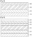
FIG. 1 is a sectional view showing a solar cell according to the embodiment. Referring toFIG. 1 , the solar cell according to the embodiment includes asupport substrate 100, aback electrode layer 200, alight absorbing layer 300, abuffer layer 400, a high-resistance window layer 500, and a low-resistance window layer 600.- The
support substrate 100 may include an insulator. For example, thesupport substrate 100 may include a glass substrate, a plastic substrate such as polymer, or a metallic substrate. In more detail, thesupport substrate 100 may include a ceramic substrate including alumina, stainless steel (SUS), or polymer having a flexible property. Thesupport substrate 100 may be transparent or may be rigid or flexible. - If the solar lime glass is used for the support substrate, sodium (Na) contained in the soda lime glass may diffuse to the CIGS
light absorbing layer 300 during the process for preparing the solar cell. In this case, the charge concentration of thelight absorbing layer 300 may be increased, so the photoelectric conversion efficiency of the solar cell may be increased. - The
back electrode layer 200 is provided on thesupport substrate 100. Theback electrode layer 200 is a conductive layer. Theback electrode layer 200 may allow the movement of charges generated from thelight absorbing layer 300, so current may flow out of the solar cell. To this end, theback electrode layer 200 may have high electric conductivity and low specific resistance. - In addition, the
back electrode layer 200 must have stability under the high temperature when the heat treatment is performed in the sulfur (S) atmosphere or selenium (Se) atmosphere, which is realized when the CIGS compound is formed. In addition, theback electrode layer 200 must have superior adhesive property with respect to thesupport substrate 100 in such a manner that theback electrode layer 200 may not be delaminated from thesupport substrate 200 due to the difference in thermal expansion coefficient. - The
back electrode layer 200 may include one selected from the group consisting of molybdenum (Mo), gold (Au), aluminum (Al), chrome (Cr), tungsten (W), and copper (Cu). Among the above materials, the Mo has a thermal expansion coefficient similar to that of thesupport substrate 100, so the Mo may improve the adhesive property and prevent theback electrode layer 200 from being delaminated from thesubstrate 100 while satisfying the characteristics required for theback electrode layer 200. - The
back electrode layer 200 may include at least two layers. In this case, the layers may be formed by using the same metal or different metals. - The light absorbing
layer 300 is provided on theback electrode layer 200. The light absorbinglayer 300 may include a P type semiconductor compound. In detail, thelight absorbing layer 300 may include a group I-III-VI2 compound. For example, thelight absorbing layer 300 may have the chalcopyrite crystal structure including CuInSe2, CuGaSe2 or Cu(In,Ga)Se2, which is the solid solution of the CuInSe2 and CuGaSe2. - The energy bandgap of the
light absorbing layer 300 is in the range of 1.04eV to 1.6eV under the normal temperature. - The
buffer layer 400 is provided on thelight absorbing layer 300. The solar cell employing the CIGS compound as thelight absorbing layer 300 may form the PN hetero junction with a semiconductor having an energy bandgap higher than that of thelight absorbing layer 300. At this time, the buffer layer is necessary when taking the difference in the crystalline structure and energy bandgap between the absorbing layer and the window layer. - The
buffer layer 400 may include CdS, which is preferred in terms of the efficiency of the solar cell. However, Cd is a hazardous heavy metal causing the environment problem. - In addition, since the
light absorbing layer 300 is formed through the printing method or the vacuum method (co-evaporation, sputtering and selenization, or MOCVD) and the low-resistance window layer 600 is formed through the vacuum method (sputtering or MOCVD), the process for forming the CdS or ZnS must be performed under the same atmosphere to improve the economic efficiency, to simplify the process and to reduce the manufacturing cost. However, according to the related art, the CdS is formed through the CBD (chemical bath deposition) scheme, so the in-line process is difficult. - In order to solve the above problem, ZnS, ZnSe, ZnO, (Zn,Mg)O, In(OH)3, In2S3, InZnSex, SnO2, or SnS2 has been suggested as a substitute for the CdS. The above materials may be deposited through the chemical bath deposition (CBD), atomic layer deposition (ALD), metal organic chemical vapor deposition (MOCVD), ion layer gas reaction (ILGAR), sputtering, thermal evaporation or electro-deposition(ED). Such solar cells are disclosed for example inPLATZER-BJORKMAN ET AL: "Zn(O,S) buffer layers by atomic layer deposition in Cu(In,Ga)Se2 based thin film solar cells: Band alignment and sulfur gradient", JOURNAL OF APPLIED PHYSICS 100, 044506 (2006) or in
US 2010/233841A1 . - Studies have been actively performed to replace CdS with ZnS. Although the CIGS solar cell including the ZnS buffer layer deposited through the CBD represents the efficiency lower than that of the solar cell employing CdS as a buffer, the CIGS solar cell including the ZnS buffer layer is suitable for the environmental-friendly requirement, so the CIGS solar cell including the ZnS buffer layer has been increasingly used.
- Among the schemes for depositing the ZnS, the CBD scheme represents the highest energy conversion efficiency. The CBD scheme can obtain the highest energy conversion efficiency because the CBD scheme is performed under the low temperature condition and the Zn-O bonding or the O-H bonding may exist as well as the ZnS compound. Actually, referring to the IR (infrared) absorption spectrum of the ZnS layer grown through the CBD scheme, the absorption band caused by the coupled vibration mode of Zn-O or O-H has been observed in addition to the absorption band caused by the coupled vibration mode of Zn and S atoms.
- According to the embodiment, the
ZnS buffer layer 400 is formed through the MOCVD scheme and the H2O precursor is applied onto thebuffer layer 400 to improve the productivity and the photoelectric conversion efficiency. TheZnS buffer layer 400 may have the hexagonal system with the energy bandgap in the range of about 3.5eV to about 3.6eV. - The high-
resistance buffer layer 500 is disposed on thebuffer layer 400. The high-resistance buffer layer 500 includes i-ZnO, which is not doped with impurities. - The low-
resistance buffer layer 600 is formed on the high-resistance buffer layer 500. The low-resistance buffer layer 600 is a transparent conductive layer. In addition, the low-resistance buffer layer 600 has resistance higher than that of theback electrode layer 200. - The low-
resistance buffer layer 600 may include oxide. For instance, the low-resistance buffer layer 600 may include one of zinc oxide (ZnO), indium tin oxide (ITO) and indium zinc oxide (IZO). - In addition, the low-
resistance buffer layer 600 may include group IIIB elements, such as B (boron) or Al (aluminum) doped zinc oxide (BZO or AZO). FIG. 2 is a graph showing variation of quantum efficiency as a function of a wavelength of light incident into the CIGS solar cell prepared by growing CdS and ZnS buffer layers through the CBD (chemical bath deposition) scheme.- As can be understood from the graph shown in
FIG. 2 , the solar cell employing ZnS as the buffer layer represents the superior quantum efficiency in the UV and IR bands as compared with the solar cell employing CdS as the buffer layer. FIG. 3 is an SEM (scanning electron microscope) photographic view of the ZnS buffer layer grown through the CBD scheme. In general, a reagent used for growing the ZnS layer through the CBD scheme may include zinc sulfate (ZnSO4) or a hydrate as a Zn precursor, thiourea;(NH2)2CS as an S precursor, and NH4OH aqueous solution (about 25 ∼ 28%) as a catalyst. A substrate is immersed in the above mixed solution and the temperature is increased in the range of 60°C to 90°C to deposit the ZnS layer.- The CBD scheme is performed under the relatively low deposition temperature, so group II metal atoms of ZnS or CdS serving as a deposition material may be prevented from diffusing to the CIGS absorbing layer serving as the substrate.
- In addition, referring to the IR (infrared) absorption spectrum of the
ZnS buffer layer 400 grown through the CBD scheme, the absorption band caused by the coupled vibration mode of Zn-O or O-H has been observed in addition to the absorption band caused by the coupled vibration mode of Zn and S atoms. - This is because the compound, such as ZnO or Zn(OH)2, besides the ZnS compound, is bonded with OH- ions extracted from NH4OH serving as the catalyst and Zn2+ ions dissociated from ZnS, so Zn(OH)2 is formed. For this reason, the ZnS layer grown through the CBD scheme is expressed as ZnS.
- That is, due to O and OH, the CIGS solar cell including the ZnS buffer grown through the CBD scheme is advantageous than the solar cell including the ZnS buffer deposited through the vacuum deposition scheme in terms of the energy conversion efficiency.
- However, as shown in
FIG. 3 , the buffer layer is not uniformly grown, and distributed in the form of small grains. In addition, since the buffer layer is grown in the liquid-phase similar to CdS, it may be difficult to simplify the manufacturing process for the CIGS solar cell. FIG. 4 is an SEM photographic view of the ZnS buffer layer prepared through the MOCVD scheme. As can be understood fromFIG. 4 , the ZnS buffer layer is uniformly grown as compared with the ZnS buffer layer grown through the CBD scheme as shown inFIG. 3 .- According to the embodiment, the ZnS buffer layer is prepared through the MOCVD scheme, so the surface of the ZnS buffer layer may be uniform. In addition, H2O is temporarily applied to the top surface of the ZnS buffer layer to form the ZnS(O,OH) layer, thereby improving the energy conversion efficiency.
FIG. 5 is a graph showing the I-V characteristic curve and power characteristic curve of the CIGS solar cell when the solar cell uses a CdS buffer prepared through the CBD scheme and a ZnS buffer prepared through the MOCVD scheme, respectively. At this time, CIGS absorbing layers have the same compositional ratio and are prepared under the same condition.- In the graph, a red line represents the CdS buffer layer and a blue line represents the ZnS buffer layer. The I-V characteristic curves of the two buffer layers were almost similar to each other. In detail, the I-V characteristic curve of the ZnS buffer layer was slightly better than that of the CdS buffer layer. Two samples shown in the graph represented the superior reverse characteristics. When taking into consideration the I-V characteristics of several solar cells in terms of the statistics, the reverse characteristic of the ZnS buffer layer was better than that of the CdS buffer layer. The I-V characteristics shown in the graph were measured in the room under the fluorescent lamp. Thus, negative values were represented in the current density. In the I-V characteristics measured under the fluorescent lamp, the light source was not the standard light source, so the curve represented random values.
- Since the energy conversion efficiency seriously relates to the characteristics of the absorbing layer, the same absorbing layer was used to compare the difference in characteristics between two buffer layers and the relative efficiency between two samples subject to the comparison may be more important than the absolute efficiency.
FIGS. 6 to 9 are sectional views showing the procedure for manufacturing the solar cell panel according to the embodiment. The above description about the solar cell will be incorporated herein by reference.- Referring to
FIGS. 6 and 7 , theback electrode layer 200 is formed on thesupport substrate 100. Theback electrode layer 200 may be deposited by using molybdenum (M). Theback electrode layer 200 may be formed through a PVD (Physical Vapor Deposition) scheme or a plating scheme. - An intervening layer, such as a diffusion-barrier layer, may be disposed between the
support substrate 100 and theback electrode layer 200. - Then, the
light absorbing layer 300 is formed on theback electrode layer 200. For instance, thelight absorbing layer 300 may be formed through various schemes such as a scheme of forming a Cu(In,Ga)Se2 (CIGS) basedlight absorbing layer 300 by simultaneously or separately evaporating Cu, In, Ga, and Se and a scheme of performing a selenization process after a metallic precursor layer has been formed. - Regarding the details of the selenization process after the formation of the metallic precursor layer, the metallic precursor layer is formed on the
back electrode layer 200 through a sputtering process employing a Cu target, an In target, a Ga target or an alloy target. - Thereafter, the metallic precursor layer is subject to the selenization process so that the Cu (In, Ga) Se2 (CIGS) based
light absorbing layer 300 is formed. - In addition, the sputtering process employing the Cu target, the In target, and the Ga target and the selenization process may be simultaneously performed.
- Further, a CIS or a CGS based light
absorbing layer 300 may be formed through the sputtering process employing only Cu and In targets or only Cu and Ga targets and the selenization process. - Referring to
FIGS. 8 and 9 , thebuffer layer 400 is formed on thelight absorbing layer 300. Thebuffer layer 400 can be formed in the temperature of 150°C to 250°C. The buffer layer includes ZnS, TEZn (triethyl zinc) can be used as a Zn precursor and t-BuSH (tert-butylthiol) can be used as an S precursor. When the compound buffer layer is grown through the MOCVD scheme, the selection of the precursor seriously relates to the growth condition and the physical property of the buffer layer. - The precursors described above are not the exclusive examples used to prepare the
ZnS buffer layer 400. For instance, the Zn precursor may include R2Zn, R2ZnNEt3 and the like (wherein, R is an alkyl group of C1∼C6, and Et is ethanol). In addition, the S precursor may include R2S, RSH, H2S gas and the like. - The
buffer layer 400 may have the thickness in the range of 10nm to 50nm, preferably, 25nm to 35nm. Since thebuffer layer 400 has a thin thickness, the growth rate of theZnS buffer layer 400 may not be serious and theZnS buffer layer 400 may have the desired thickness within a short period of time even if the substrate temperature is relatively low when theZnS buffer layer 400 is grown through the MOCVD scheme. Thus, the low growth temperature can be adopted, so that the Zn atoms can be prevented from diffusing to the CIGS absorbing layer. - In general, an ionic radius of a Zn atom is about 7.4x10⁻¹⁰m and an ionic radius of a Cd atom is about 9.7x10⁻¹⁰m. When comparing with the ionic radius of a Cu atom (about 7.2x10⁻¹⁰m), the ionic radius of the Zn atom is closer to the ionic radius of the Cu atom.
- For this reason, the diffusivity of the Zn atoms in the CIGS absorbing layer is significantly greater than that of the Cd atoms and the Zn atoms may be readily diffused under the relatively low temperature, so the Zn atoms may substitutes for VCu so that ZnCu is formed. The defect derived from the above reaction may serve as a donor and the donor changes the conductive characteristic of the P type CIGS absorbing layer, thereby lowering the energy conversion efficiency or causing the short.
- As described above, even if the ZnS buffer layer is prepared under the relatively low substrate temperature, the Zn atoms may diffuse into the CIGS absorbing layer so that the electric characteristic of the CIGS absorbing layer may be changed.
- According to the embodiment, in order to prevent the Zn atoms from diffusing into the CIGS absorbing layer, the S precursor is primarily applied to the
light absorbing layer 300 to ensure the S atmosphere and then the Z precursor is applied to form the ZnS compound through the reaction between the Zn atoms and the S atoms, thereby preventing the Zn atoms from diffusing into thelight absorbing layer 300. - Since the S precursor is primarily applied, the S density may have the maximum value at the lower portion of the
buffer layer 400. - Referring to the I-V characteristic of samples, which were prepared by varying the turn-on time of the S precursor and the Zn precursor, the short was represented in all samples when the S precursor was not primarily applied or the Zn precursor was primarily applied, and the superior I-V characteristic was obtained when the Zn precursor was applied after primarily applying the S precursor.
- The short represents that the acceptor level by VCu formed in the P type CIGS absorbing layer is changed to the ZnCu donor level due to the diffusion of the Zn atoms, so that the electric characteristic is changed into the electric characteristic of an N type CIGS absorbing layer.
- After forming the
ZnS buffer layer 400 through the MOCVD scheme, H2O is applied to the surface of theZnS buffer layer 400 for a predetermined time by using the H2O precursor before the ZnO high-resistance window layer 500 is formed to change theZnS buffer layer 400 into ZnS (O, OH), and then the Zn precursor is applied to form the i-ZnO high-resistance window layer 500. - The solar cell, which is prepared by primarily applying vapor of the H2O precursor onto the
substrate 100 loaded in the chamber for a predetermined time and then applying vapor of the Zn precursor, represents the superior I-V characteristics. This is because ZnO or Zn(OH)2 is partially created in theZnS buffer layer 400, so theZnS buffer layer 400 is similar to the buffer layer grown through the CBD scheme, so that the I-V characteristics can be improved. - Then, the low-
resistance window layer 600 is formed on the high-resistance window layer 500. In general, the low-resistance window layer 600 is deposited by using the material used for the high-resistance window layer 500. At this time, the dopant is also deposited to impart the conductive characteristic to the low-resistance window layer 600.
Claims (4)
- A method of preparing a CIGS solar cell, the method comprising:forming a back electrode layer (200) on a substrate (100);forming a light absorbing layer (300) on the back electrode layer (200);forming a buffer layer (400) including ZnS on the light absorbing layer (300) through an MOCVD(Metal Organic Chemical Vapor Deposition) scheme by injecting a Zn precursor and an S precursor onto the light absorbing layer (300); andforming a window layer (500) on the buffer layer (400),wherein the forming of the buffer layer (400) comprises:applying a S precursor to the light absorbing layer (300), thenapplying a Zn precursor to the light absorbing layer (300) in order to form the buffer layer (400) including ZnS compound through the reaction between the Zn atoms and the S atoms,applying H2O onto the buffer layer (400) to convert ZnS into ZnS(O, OH).
- The method of claim 1, wherein the Zn precursor includes at least one of TEZn, R2Zn, and R2ZnNEt3 and the S precursor includes at least one of tert-butylthiol (t-BuSH), R2S, RSH, and H2S gas, where R is an alkyl group of C1∼C6 and Et is ethanol.
- The method of claim 1, wherein the buffer layer (400) is formed at a temperature in a range of 150°C to 250°C.
- The method of claim 1, wherein, after forming the ZnS buffer layer (400) through the MOCVD, H2O is applied to the surface of the ZnS buffer layer (400) for a predetermined time by using the H2O precursor before the ZnO high-resistance window layer (500) is formed to change the ZnS buffer layer (400) into ZnS (O, OH), and then the Zn precursor is applied to form the i-ZnO high-resistance window layer (500).
Applications Claiming Priority (2)
| Application Number | Priority Date | Filing Date | Title |
|---|---|---|---|
| KR1020110039051AKR101210171B1 (en) | 2011-04-26 | 2011-04-26 | Solar cell apparatus and method of fabricating the same |
| PCT/KR2012/003270WO2012148208A2 (en) | 2011-04-26 | 2012-04-26 | Solar cell and method of preparing the same |
Publications (3)
| Publication Number | Publication Date |
|---|---|
| EP2702615A2 EP2702615A2 (en) | 2014-03-05 |
| EP2702615A4 EP2702615A4 (en) | 2014-09-03 |
| EP2702615B1true EP2702615B1 (en) | 2020-03-11 |
Family
ID=47072931
Family Applications (1)
| Application Number | Title | Priority Date | Filing Date |
|---|---|---|---|
| EP12777257.2AActiveEP2702615B1 (en) | 2011-04-26 | 2012-04-26 | Method of preparing a solar cell |
Country Status (5)
| Country | Link |
|---|---|
| US (1) | US20140048132A1 (en) |
| EP (1) | EP2702615B1 (en) |
| KR (1) | KR101210171B1 (en) |
| CN (1) | CN103620792B (en) |
| WO (1) | WO2012148208A2 (en) |
Families Citing this family (4)
| Publication number | Priority date | Publication date | Assignee | Title |
|---|---|---|---|---|
| US9379259B2 (en)* | 2012-11-05 | 2016-06-28 | International Business Machines Corporation | Double layered transparent conductive oxide for reduced schottky barrier in photovoltaic devices |
| US9574135B2 (en)* | 2013-08-22 | 2017-02-21 | Nanoco Technologies Ltd. | Gas phase enhancement of emission color quality in solid state LEDs |
| KR101765987B1 (en)* | 2014-01-22 | 2017-08-08 | 한양대학교 산학협력단 | Solar cell and method of fabricating the same |
| CN109545869A (en)* | 2018-10-24 | 2019-03-29 | 四川大学 | A kind of flexible cadmium telluride solar cell of two-sided three terminal |
Citations (2)
| Publication number | Priority date | Publication date | Assignee | Title |
|---|---|---|---|---|
| CN1285129C (en)* | 2003-12-09 | 2006-11-15 | 南开大学 | Method for preparing buffer layer film of cadmium-free copper-indium-gallium-selenium thin-film solar cell |
| US20100210064A1 (en)* | 2008-05-19 | 2010-08-19 | Showa Shell Sekiyu K.K. | Method for manufacturing cis-based thin film solar cell |
Family Cites Families (6)
| Publication number | Priority date | Publication date | Assignee | Title |
|---|---|---|---|---|
| SE0301350D0 (en)* | 2003-05-08 | 2003-05-08 | Forskarpatent I Uppsala Ab | A thin-film solar cell |
| JP4841173B2 (en)* | 2005-05-27 | 2011-12-21 | 昭和シェル石油株式会社 | High resistance buffer layer / window layer continuous film forming method and film forming apparatus for CIS thin film solar cell |
| JP5180188B2 (en)* | 2007-03-28 | 2013-04-10 | 昭和シェル石油株式会社 | CIS-based thin film solar cell device manufacturing method |
| KR101012847B1 (en)* | 2008-08-27 | 2011-02-08 | 부산대학교 산학협력단 | Method for manufacturing compound solar cell using nanorod and compound solar cell |
| KR20110012314A (en)* | 2009-07-30 | 2011-02-09 | 엘지전자 주식회사 | Thin film solar cell and manufacturing method thereof |
| KR20110013009A (en)* | 2009-07-31 | 2011-02-09 | 엘지전자 주식회사 | Thin film solar cell having a plurality of back electrode layers and manufacturing method thereof |
- 2011
- 2011-04-26KRKR1020110039051Apatent/KR101210171B1/ennot_activeExpired - Fee Related
- 2012
- 2012-04-26EPEP12777257.2Apatent/EP2702615B1/enactiveActive
- 2012-04-26USUS14/114,203patent/US20140048132A1/ennot_activeAbandoned
- 2012-04-26WOPCT/KR2012/003270patent/WO2012148208A2/enactiveApplication Filing
- 2012-04-26CNCN201280031463.3Apatent/CN103620792B/ennot_activeExpired - Fee Related
Patent Citations (2)
| Publication number | Priority date | Publication date | Assignee | Title |
|---|---|---|---|---|
| CN1285129C (en)* | 2003-12-09 | 2006-11-15 | 南开大学 | Method for preparing buffer layer film of cadmium-free copper-indium-gallium-selenium thin-film solar cell |
| US20100210064A1 (en)* | 2008-05-19 | 2010-08-19 | Showa Shell Sekiyu K.K. | Method for manufacturing cis-based thin film solar cell |
Also Published As
| Publication number | Publication date |
|---|---|
| WO2012148208A3 (en) | 2013-03-21 |
| EP2702615A2 (en) | 2014-03-05 |
| KR101210171B1 (en) | 2012-12-07 |
| WO2012148208A2 (en) | 2012-11-01 |
| EP2702615A4 (en) | 2014-09-03 |
| CN103620792B (en) | 2017-02-08 |
| KR20120121210A (en) | 2012-11-05 |
| US20140048132A1 (en) | 2014-02-20 |
| CN103620792A (en) | 2014-03-05 |
Similar Documents
| Publication | Publication Date | Title |
|---|---|---|
| Regmi et al. | Perspectives of chalcopyrite-based CIGSe thin-film solar cell: a review | |
| Song et al. | A review on development prospect of CZTS based thin film solar cells | |
| EP2410556A2 (en) | Sodium sputtering doping method for large scale CIGS based thin film photovoltaic materials | |
| EP2306524A2 (en) | In chamber sodium doping process and system for large scale fabrication of cigs based thin film photovoltaic materials | |
| US20100319777A1 (en) | Solar cell and method of fabricating the same | |
| KR101628312B1 (en) | PREPARATION METHOD OF CZTSSe-BASED THIN FILM SOLAR CELL AND CZTSSe-BASED THIN FILM SOLAR CELL PREPARED BY THE METHOD | |
| US20140326296A1 (en) | Solar cell and method of fabricating the same | |
| CN102652368A (en) | Cu-In-Zn-Sn-(Se,S)-based thin film used in solar cell and manufacturing method thereof | |
| Saha | A Status Review on Cu2ZnSn (S, Se) 4‐Based Thin‐Film Solar Cells | |
| US20140182665A1 (en) | Optical Absorbers | |
| JP2011129631A (en) | Method of manufacturing cis thin film solar cell | |
| US8728855B2 (en) | Method of processing a semiconductor assembly | |
| EP2702615B1 (en) | Method of preparing a solar cell | |
| CN104051565A (en) | Method of making photovoltaic device | |
| US20140370646A1 (en) | Absorber layer for a thin film photovoltaic device with a double-graded band gap | |
| JP6035122B2 (en) | Photoelectric conversion element and method for producing buffer layer of photoelectric conversion element | |
| US8119513B1 (en) | Method for making cadmium sulfide layer | |
| CN105474371B (en) | Layer system for the thin-layer solar cell with sodium indium sulfide cushion | |
| KR20140047760A (en) | Manufacturing method of solar cell light absortion layer | |
| US8809105B2 (en) | Method of processing a semiconductor assembly | |
| WO2010150864A1 (en) | Cis-based thin film solar cell | |
| KR102057234B1 (en) | Preparation of CIGS thin film solar cell and CIGS thin film solar cell using the same | |
| KR101807118B1 (en) | PV Device with Graded Grain Size and S:Se Ratio | |
| CN102447008A (en) | Photovoltaic device and method for making | |
| JP5575163B2 (en) | CIS type thin film solar cell manufacturing method |
Legal Events
| Date | Code | Title | Description |
|---|---|---|---|
| PUAI | Public reference made under article 153(3) epc to a published international application that has entered the european phase | Free format text:ORIGINAL CODE: 0009012 | |
| 17P | Request for examination filed | Effective date:20131031 | |
| AK | Designated contracting states | Kind code of ref document:A2 Designated state(s):AL AT BE BG CH CY CZ DE DK EE ES FI FR GB GR HR HU IE IS IT LI LT LU LV MC MK MT NL NO PL PT RO RS SE SI SK SM TR | |
| DAX | Request for extension of the european patent (deleted) | ||
| A4 | Supplementary search report drawn up and despatched | Effective date:20140805 | |
| RIC1 | Information provided on ipc code assigned before grant | Ipc:H01L 31/0749 20120101ALI20140730BHEP Ipc:H01L 31/0296 20060101ALI20140730BHEP Ipc:H01L 31/0216 20140101ALI20140730BHEP Ipc:H01L 31/042 20140101AFI20140730BHEP Ipc:H01L 31/0224 20060101ALI20140730BHEP Ipc:H01L 31/18 20060101ALI20140730BHEP | |
| RAP1 | Party data changed (applicant data changed or rights of an application transferred) | Owner name:CHUNG-ANG UNIVERSITY INDUSTRY-ACADEMY COOPERATION Owner name:LG INNOTEK CO., LTD. | |
| STAA | Information on the status of an ep patent application or granted ep patent | Free format text:STATUS: EXAMINATION IS IN PROGRESS | |
| 17Q | First examination report despatched | Effective date:20190513 | |
| GRAP | Despatch of communication of intention to grant a patent | Free format text:ORIGINAL CODE: EPIDOSNIGR1 | |
| STAA | Information on the status of an ep patent application or granted ep patent | Free format text:STATUS: GRANT OF PATENT IS INTENDED | |
| INTG | Intention to grant announced | Effective date:20191022 | |
| GRAS | Grant fee paid | Free format text:ORIGINAL CODE: EPIDOSNIGR3 | |
| GRAA | (expected) grant | Free format text:ORIGINAL CODE: 0009210 | |
| STAA | Information on the status of an ep patent application or granted ep patent | Free format text:STATUS: THE PATENT HAS BEEN GRANTED | |
| AK | Designated contracting states | Kind code of ref document:B1 Designated state(s):AL AT BE BG CH CY CZ DE DK EE ES FI FR GB GR HR HU IE IS IT LI LT LU LV MC MK MT NL NO PL PT RO RS SE SI SK SM TR | |
| REG | Reference to a national code | Ref country code:GB Ref legal event code:FG4D | |
| REG | Reference to a national code | Ref country code:CH Ref legal event code:EP | |
| REG | Reference to a national code | Ref country code:AT Ref legal event code:REF Ref document number:1244239 Country of ref document:AT Kind code of ref document:T Effective date:20200315 | |
| REG | Reference to a national code | Ref country code:DE Ref legal event code:R096 Ref document number:602012068413 Country of ref document:DE | |
| REG | Reference to a national code | Ref country code:IE Ref legal event code:FG4D | |
| PG25 | Lapsed in a contracting state [announced via postgrant information from national office to epo] | Ref country code:RS Free format text:LAPSE BECAUSE OF FAILURE TO SUBMIT A TRANSLATION OF THE DESCRIPTION OR TO PAY THE FEE WITHIN THE PRESCRIBED TIME-LIMIT Effective date:20200311 Ref country code:FI Free format text:LAPSE BECAUSE OF FAILURE TO SUBMIT A TRANSLATION OF THE DESCRIPTION OR TO PAY THE FEE WITHIN THE PRESCRIBED TIME-LIMIT Effective date:20200311 Ref country code:NO Free format text:LAPSE BECAUSE OF FAILURE TO SUBMIT A TRANSLATION OF THE DESCRIPTION OR TO PAY THE FEE WITHIN THE PRESCRIBED TIME-LIMIT Effective date:20200611 | |
| REG | Reference to a national code | Ref country code:NL Ref legal event code:MP Effective date:20200311 | |
| PG25 | Lapsed in a contracting state [announced via postgrant information from national office to epo] | Ref country code:SE Free format text:LAPSE BECAUSE OF FAILURE TO SUBMIT A TRANSLATION OF THE DESCRIPTION OR TO PAY THE FEE WITHIN THE PRESCRIBED TIME-LIMIT Effective date:20200311 Ref country code:LV Free format text:LAPSE BECAUSE OF FAILURE TO SUBMIT A TRANSLATION OF THE DESCRIPTION OR TO PAY THE FEE WITHIN THE PRESCRIBED TIME-LIMIT Effective date:20200311 Ref country code:HR Free format text:LAPSE BECAUSE OF FAILURE TO SUBMIT A TRANSLATION OF THE DESCRIPTION OR TO PAY THE FEE WITHIN THE PRESCRIBED TIME-LIMIT Effective date:20200311 Ref country code:GR Free format text:LAPSE BECAUSE OF FAILURE TO SUBMIT A TRANSLATION OF THE DESCRIPTION OR TO PAY THE FEE WITHIN THE PRESCRIBED TIME-LIMIT Effective date:20200612 Ref country code:BG Free format text:LAPSE BECAUSE OF FAILURE TO SUBMIT A TRANSLATION OF THE DESCRIPTION OR TO PAY THE FEE WITHIN THE PRESCRIBED TIME-LIMIT Effective date:20200611 | |
| REG | Reference to a national code | Ref country code:LT Ref legal event code:MG4D | |
| PG25 | Lapsed in a contracting state [announced via postgrant information from national office to epo] | Ref country code:NL Free format text:LAPSE BECAUSE OF FAILURE TO SUBMIT A TRANSLATION OF THE DESCRIPTION OR TO PAY THE FEE WITHIN THE PRESCRIBED TIME-LIMIT Effective date:20200311 | |
| PG25 | Lapsed in a contracting state [announced via postgrant information from national office to epo] | Ref country code:RO Free format text:LAPSE BECAUSE OF FAILURE TO SUBMIT A TRANSLATION OF THE DESCRIPTION OR TO PAY THE FEE WITHIN THE PRESCRIBED TIME-LIMIT Effective date:20200311 Ref country code:IS Free format text:LAPSE BECAUSE OF FAILURE TO SUBMIT A TRANSLATION OF THE DESCRIPTION OR TO PAY THE FEE WITHIN THE PRESCRIBED TIME-LIMIT Effective date:20200711 Ref country code:CZ Free format text:LAPSE BECAUSE OF FAILURE TO SUBMIT A TRANSLATION OF THE DESCRIPTION OR TO PAY THE FEE WITHIN THE PRESCRIBED TIME-LIMIT Effective date:20200311 Ref country code:SK Free format text:LAPSE BECAUSE OF FAILURE TO SUBMIT A TRANSLATION OF THE DESCRIPTION OR TO PAY THE FEE WITHIN THE PRESCRIBED TIME-LIMIT Effective date:20200311 Ref country code:PT Free format text:LAPSE BECAUSE OF FAILURE TO SUBMIT A TRANSLATION OF THE DESCRIPTION OR TO PAY THE FEE WITHIN THE PRESCRIBED TIME-LIMIT Effective date:20200805 Ref country code:LT Free format text:LAPSE BECAUSE OF FAILURE TO SUBMIT A TRANSLATION OF THE DESCRIPTION OR TO PAY THE FEE WITHIN THE PRESCRIBED TIME-LIMIT Effective date:20200311 Ref country code:SM Free format text:LAPSE BECAUSE OF FAILURE TO SUBMIT A TRANSLATION OF THE DESCRIPTION OR TO PAY THE FEE WITHIN THE PRESCRIBED TIME-LIMIT Effective date:20200311 Ref country code:EE Free format text:LAPSE BECAUSE OF FAILURE TO SUBMIT A TRANSLATION OF THE DESCRIPTION OR TO PAY THE FEE WITHIN THE PRESCRIBED TIME-LIMIT Effective date:20200311 | |
| REG | Reference to a national code | Ref country code:AT Ref legal event code:MK05 Ref document number:1244239 Country of ref document:AT Kind code of ref document:T Effective date:20200311 | |
| REG | Reference to a national code | Ref country code:CH Ref legal event code:PL | |
| REG | Reference to a national code | Ref country code:DE Ref legal event code:R097 Ref document number:602012068413 Country of ref document:DE | |
| PG25 | Lapsed in a contracting state [announced via postgrant information from national office to epo] | Ref country code:MC Free format text:LAPSE BECAUSE OF FAILURE TO SUBMIT A TRANSLATION OF THE DESCRIPTION OR TO PAY THE FEE WITHIN THE PRESCRIBED TIME-LIMIT Effective date:20200311 | |
| PLBE | No opposition filed within time limit | Free format text:ORIGINAL CODE: 0009261 | |
| STAA | Information on the status of an ep patent application or granted ep patent | Free format text:STATUS: NO OPPOSITION FILED WITHIN TIME LIMIT | |
| PG25 | Lapsed in a contracting state [announced via postgrant information from national office to epo] | Ref country code:AT Free format text:LAPSE BECAUSE OF FAILURE TO SUBMIT A TRANSLATION OF THE DESCRIPTION OR TO PAY THE FEE WITHIN THE PRESCRIBED TIME-LIMIT Effective date:20200311 Ref country code:ES Free format text:LAPSE BECAUSE OF FAILURE TO SUBMIT A TRANSLATION OF THE DESCRIPTION OR TO PAY THE FEE WITHIN THE PRESCRIBED TIME-LIMIT Effective date:20200311 Ref country code:CH Free format text:LAPSE BECAUSE OF NON-PAYMENT OF DUE FEES Effective date:20200430 Ref country code:LI Free format text:LAPSE BECAUSE OF NON-PAYMENT OF DUE FEES Effective date:20200430 Ref country code:IT Free format text:LAPSE BECAUSE OF FAILURE TO SUBMIT A TRANSLATION OF THE DESCRIPTION OR TO PAY THE FEE WITHIN THE PRESCRIBED TIME-LIMIT Effective date:20200311 Ref country code:LU Free format text:LAPSE BECAUSE OF NON-PAYMENT OF DUE FEES Effective date:20200426 Ref country code:DK Free format text:LAPSE BECAUSE OF FAILURE TO SUBMIT A TRANSLATION OF THE DESCRIPTION OR TO PAY THE FEE WITHIN THE PRESCRIBED TIME-LIMIT Effective date:20200311 | |
| REG | Reference to a national code | Ref country code:BE Ref legal event code:MM Effective date:20200430 | |
| 26N | No opposition filed | Effective date:20201214 | |
| PG25 | Lapsed in a contracting state [announced via postgrant information from national office to epo] | Ref country code:BE Free format text:LAPSE BECAUSE OF NON-PAYMENT OF DUE FEES Effective date:20200430 Ref country code:PL Free format text:LAPSE BECAUSE OF FAILURE TO SUBMIT A TRANSLATION OF THE DESCRIPTION OR TO PAY THE FEE WITHIN THE PRESCRIBED TIME-LIMIT Effective date:20200311 Ref country code:SI Free format text:LAPSE BECAUSE OF FAILURE TO SUBMIT A TRANSLATION OF THE DESCRIPTION OR TO PAY THE FEE WITHIN THE PRESCRIBED TIME-LIMIT Effective date:20200311 | |
| GBPC | Gb: european patent ceased through non-payment of renewal fee | Effective date:20200611 | |
| PG25 | Lapsed in a contracting state [announced via postgrant information from national office to epo] | Ref country code:IE Free format text:LAPSE BECAUSE OF NON-PAYMENT OF DUE FEES Effective date:20200426 Ref country code:GB Free format text:LAPSE BECAUSE OF NON-PAYMENT OF DUE FEES Effective date:20200611 Ref country code:FR Free format text:LAPSE BECAUSE OF NON-PAYMENT OF DUE FEES Effective date:20200511 | |
| PG25 | Lapsed in a contracting state [announced via postgrant information from national office to epo] | Ref country code:TR Free format text:LAPSE BECAUSE OF FAILURE TO SUBMIT A TRANSLATION OF THE DESCRIPTION OR TO PAY THE FEE WITHIN THE PRESCRIBED TIME-LIMIT Effective date:20200311 Ref country code:MT Free format text:LAPSE BECAUSE OF FAILURE TO SUBMIT A TRANSLATION OF THE DESCRIPTION OR TO PAY THE FEE WITHIN THE PRESCRIBED TIME-LIMIT Effective date:20200311 Ref country code:CY Free format text:LAPSE BECAUSE OF FAILURE TO SUBMIT A TRANSLATION OF THE DESCRIPTION OR TO PAY THE FEE WITHIN THE PRESCRIBED TIME-LIMIT Effective date:20200311 | |
| PG25 | Lapsed in a contracting state [announced via postgrant information from national office to epo] | Ref country code:MK Free format text:LAPSE BECAUSE OF FAILURE TO SUBMIT A TRANSLATION OF THE DESCRIPTION OR TO PAY THE FEE WITHIN THE PRESCRIBED TIME-LIMIT Effective date:20200311 Ref country code:AL Free format text:LAPSE BECAUSE OF FAILURE TO SUBMIT A TRANSLATION OF THE DESCRIPTION OR TO PAY THE FEE WITHIN THE PRESCRIBED TIME-LIMIT Effective date:20200311 | |
| REG | Reference to a national code | Ref country code:DE Ref legal event code:R079 Ref document number:602012068413 Country of ref document:DE Free format text:PREVIOUS MAIN CLASS: H01L0031042000 Ipc:H10F0019000000 | |
| PGFP | Annual fee paid to national office [announced via postgrant information from national office to epo] | Ref country code:DE Payment date:20250320 Year of fee payment:14 |