EP2667323B1 - Multi-mode RFID tag architecture - Google Patents
Multi-mode RFID tag architectureDownload PDFInfo
- Publication number
- EP2667323B1 EP2667323B1EP13003869.8AEP13003869AEP2667323B1EP 2667323 B1EP2667323 B1EP 2667323B1EP 13003869 AEP13003869 AEP 13003869AEP 2667323 B1EP2667323 B1EP 2667323B1
- Authority
- EP
- European Patent Office
- Prior art keywords
- mode
- field mode
- signal
- near field
- rfid
- Prior art date
- Legal status (The legal status is an assumption and is not a legal conclusion. Google has not performed a legal analysis and makes no representation as to the accuracy of the status listed.)
- Not-in-force
Links
Images


Classifications
- H—ELECTRICITY
- H04—ELECTRIC COMMUNICATION TECHNIQUE
- H04B—TRANSMISSION
- H04B5/00—Near-field transmission systems, e.g. inductive or capacitive transmission systems
- H04B5/40—Near-field transmission systems, e.g. inductive or capacitive transmission systems characterised by components specially adapted for near-field transmission
- H04B5/48—Transceivers
- G—PHYSICS
- G06—COMPUTING OR CALCULATING; COUNTING
- G06K—GRAPHICAL DATA READING; PRESENTATION OF DATA; RECORD CARRIERS; HANDLING RECORD CARRIERS
- G06K7/00—Methods or arrangements for sensing record carriers, e.g. for reading patterns
- G06K7/10—Methods or arrangements for sensing record carriers, e.g. for reading patterns by electromagnetic radiation, e.g. optical sensing; by corpuscular radiation
- G06K7/10009—Methods or arrangements for sensing record carriers, e.g. for reading patterns by electromagnetic radiation, e.g. optical sensing; by corpuscular radiation sensing by radiation using wavelengths larger than 0.1 mm, e.g. radio-waves or microwaves
- G06K7/10198—Methods or arrangements for sensing record carriers, e.g. for reading patterns by electromagnetic radiation, e.g. optical sensing; by corpuscular radiation sensing by radiation using wavelengths larger than 0.1 mm, e.g. radio-waves or microwaves setting parameters for the interrogator, e.g. programming parameters and operating modes
- G—PHYSICS
- G06—COMPUTING OR CALCULATING; COUNTING
- G06K—GRAPHICAL DATA READING; PRESENTATION OF DATA; RECORD CARRIERS; HANDLING RECORD CARRIERS
- G06K19/00—Record carriers for use with machines and with at least a part designed to carry digital markings
- G06K19/06—Record carriers for use with machines and with at least a part designed to carry digital markings characterised by the kind of the digital marking, e.g. shape, nature, code
- G06K19/067—Record carriers with conductive marks, printed circuits or semiconductor circuit elements, e.g. credit or identity cards also with resonating or responding marks without active components
- G06K19/07—Record carriers with conductive marks, printed circuits or semiconductor circuit elements, e.g. credit or identity cards also with resonating or responding marks without active components with integrated circuit chips
- G06K19/0723—Record carriers with conductive marks, printed circuits or semiconductor circuit elements, e.g. credit or identity cards also with resonating or responding marks without active components with integrated circuit chips the record carrier comprising an arrangement for non-contact communication, e.g. wireless communication circuits on transponder cards, non-contact smart cards or RFIDs
- G06K19/0724—Record carriers with conductive marks, printed circuits or semiconductor circuit elements, e.g. credit or identity cards also with resonating or responding marks without active components with integrated circuit chips the record carrier comprising an arrangement for non-contact communication, e.g. wireless communication circuits on transponder cards, non-contact smart cards or RFIDs the arrangement being a circuit for communicating at a plurality of frequencies, e.g. for managing time multiplexed communication over at least two antennas of different types
- G—PHYSICS
- G06—COMPUTING OR CALCULATING; COUNTING
- G06K—GRAPHICAL DATA READING; PRESENTATION OF DATA; RECORD CARRIERS; HANDLING RECORD CARRIERS
- G06K19/00—Record carriers for use with machines and with at least a part designed to carry digital markings
- G06K19/06—Record carriers for use with machines and with at least a part designed to carry digital markings characterised by the kind of the digital marking, e.g. shape, nature, code
- G06K19/067—Record carriers with conductive marks, printed circuits or semiconductor circuit elements, e.g. credit or identity cards also with resonating or responding marks without active components
- G06K19/07—Record carriers with conductive marks, printed circuits or semiconductor circuit elements, e.g. credit or identity cards also with resonating or responding marks without active components with integrated circuit chips
- G06K19/073—Special arrangements for circuits, e.g. for protecting identification code in memory
- G—PHYSICS
- G06—COMPUTING OR CALCULATING; COUNTING
- G06K—GRAPHICAL DATA READING; PRESENTATION OF DATA; RECORD CARRIERS; HANDLING RECORD CARRIERS
- G06K19/00—Record carriers for use with machines and with at least a part designed to carry digital markings
- G06K19/06—Record carriers for use with machines and with at least a part designed to carry digital markings characterised by the kind of the digital marking, e.g. shape, nature, code
- G06K19/067—Record carriers with conductive marks, printed circuits or semiconductor circuit elements, e.g. credit or identity cards also with resonating or responding marks without active components
- G06K19/07—Record carriers with conductive marks, printed circuits or semiconductor circuit elements, e.g. credit or identity cards also with resonating or responding marks without active components with integrated circuit chips
- G06K19/077—Constructional details, e.g. mounting of circuits in the carrier
- G06K19/07749—Constructional details, e.g. mounting of circuits in the carrier the record carrier being capable of non-contact communication, e.g. constructional details of the antenna of a non-contact smart card
- G06K19/07766—Constructional details, e.g. mounting of circuits in the carrier the record carrier being capable of non-contact communication, e.g. constructional details of the antenna of a non-contact smart card comprising at least a second communication arrangement in addition to a first non-contact communication arrangement
- G—PHYSICS
- G06—COMPUTING OR CALCULATING; COUNTING
- G06K—GRAPHICAL DATA READING; PRESENTATION OF DATA; RECORD CARRIERS; HANDLING RECORD CARRIERS
- G06K7/00—Methods or arrangements for sensing record carriers, e.g. for reading patterns
- G06K7/0008—General problems related to the reading of electronic memory record carriers, independent of its reading method, e.g. power transfer
- H—ELECTRICITY
- H04—ELECTRIC COMMUNICATION TECHNIQUE
- H04B—TRANSMISSION
- H04B5/00—Near-field transmission systems, e.g. inductive or capacitive transmission systems
- H—ELECTRICITY
- H04—ELECTRIC COMMUNICATION TECHNIQUE
- H04B—TRANSMISSION
- H04B5/00—Near-field transmission systems, e.g. inductive or capacitive transmission systems
- H04B5/20—Near-field transmission systems, e.g. inductive or capacitive transmission systems characterised by the transmission technique; characterised by the transmission medium
- H04B5/22—Capacitive coupling
- H—ELECTRICITY
- H04—ELECTRIC COMMUNICATION TECHNIQUE
- H04B—TRANSMISSION
- H04B5/00—Near-field transmission systems, e.g. inductive or capacitive transmission systems
- H04B5/20—Near-field transmission systems, e.g. inductive or capacitive transmission systems characterised by the transmission technique; characterised by the transmission medium
- H04B5/24—Inductive coupling
- H04B5/26—Inductive coupling using coils
- H04B5/263—Multiple coils at either side
- H—ELECTRICITY
- H04—ELECTRIC COMMUNICATION TECHNIQUE
- H04B—TRANSMISSION
- H04B5/00—Near-field transmission systems, e.g. inductive or capacitive transmission systems
- H04B5/70—Near-field transmission systems, e.g. inductive or capacitive transmission systems specially adapted for specific purposes
- H04B5/77—Near-field transmission systems, e.g. inductive or capacitive transmission systems specially adapted for specific purposes for interrogation
Definitions
- This inventionrelates generally to communication systems and more particularly to RFID systems.
- a radio frequency identification (RFID) systemgenerally includes a reader, also known as an interrogator, and a remote tag, also known as a transponder. Each tag stores identification or other data for use in identifying a person, item, pallet or other object or data related to a characteristic of a person, item, pallet or other object. RFID systems may use active tags that include an internal power source, such as a battery, and/or passive tags that do not contain an internal power source, but instead are remotely powered by the reader.
- RFIDradio frequency identification
- RFIDradio frequency
- the RFID readerto access the identification data stored on an RFID tag, the RFID reader generates a modulated RF interrogation signal designed to evoke a modulated RF response from a tag.
- the RF response from the tagincludes the coded data stored in the RFID tag.
- the RFID readerdecodes the coded data to identify or determine the characteristics of a person, item, pallet or other object associated with the RFID tag.
- the RFID readeralso generates an unmodulated, continuous wave (CW) signal to activate and power the tag during data transfer.
- CWcontinuous wave
- passive tagsobtain power from transmissions of the RFID reader.
- Active tagsinclude a battery and have greater ability to power transceivers, processer, memory and other on-tag devices.
- RFID systemstypically employ either far field or near field technology.
- far field technologythe distance between the reader and the tag is great compared to the wavelength of the carrier signal.
- far field technologyuses carrier signals in the ultra high frequency or microwave frequency ranges.
- the RFID readergenerates and transmits an RF signal via an antenna to all tags within range of the antenna.
- One or more of the tags that receive the RF signalresponds to the reader using a backscattering technique in which the tags modulate and reflect the received RF signal.
- the operating distanceis usually less than one wavelength of the carrier signal.
- the reading rangeis approximately limited to 20 cm or less depending on the frequency.
- the RFID reader and tagcommunicate via electromagnetic or inductive coupling between the coils of the reader and the tag.
- the near field technologyuses carrier signals in the low frequency range.
- RFID tagshave used a multilayer coil (e.g., 3 layers of 100-150 turns each) wrapped around a metal core at lower frequencies of 135 KHz.
- RFID tagshave used a planar spiral coil inductor with 5-7 turns over a credit-card-sized form factor.
- Such tag coil antennasare large in comparison to the other modules of the RFID tag and are not able to be integrated on a chip, such as a complementary metal-oxide-semiconductor (CMOS), bipolar complementary metal-oxide-semiconductor (BiCMOS) or gallium arsenide (GaAs) integrated circuit, with other modules of the RFID tag.
- CMOScomplementary metal-oxide-semiconductor
- BiCMOSbipolar complementary metal-oxide-semiconductor
- GaAsgallium arsenide
- the International Organization for Standardizationhas developed an RFID standard called the ISO 18000 series.
- the ISO 18000 series standarddescribes air interface protocols for RFID systems especially in applications used to track items in a supply chain.
- the ISO 18000 serieshas seven parts to cover the major frequencies used in RFID systems around the world. The seven parts are:
- near-field technology with magnetic/inductive couplinghas an air interface protocol at low frequency (LF) of 135 KHz or less or at 13.56 high frequency (HF).
- LFlow frequency
- HFhigh frequency
- ISO 18000-3defines two modes. In mode 1, the tag to reader data rate is 26.48 kbps while mode 2 is a high speed interface of 105.9375 kbps on each of 8 channels.
- the communication protocol used by the reader and the tagis typically a load modulation technique.
- Far field technology with RF backscatter couplinghas three ISO defined air interfaces at 2.45 GHz microwave frequency according to ISO 18000-5, 860MHZ to 930 MHz ultra high frequency (UHF) range according to ISO 18000-6 and 433.92 MHz UHF according to ISO 18000-7.
- UHFultra high frequency
- the ISO 18000-6has defined two tag types, Type A and Type B with a tag to reader link defined as including 40kbps data rate, Amplitude Shift Keying (ASK) modulation, and biphase-space or FM0 encoding of data.
- ASKAmplitude Shift Keying
- the EPCglobal Class 1, Generation 2 standarddefines a tag standard using UHF with a tag to reader link of 40 to 640 kbps, ASK or Phase Shift Keying (PSK) modulation and data encoding of FMO or Miller-modulated subcarrier.
- ASKPhase Shift Keying
- tags employing near field technology operating at LF or HFhave been used in applications involving item-level tagging for inventory control in the supply chain management or applications involving short range reads such as smart cards or vicinity credit cards, e.g. for access control or monetary use, passports, money bills authentication, bank documents, etc. Such applications do not need long range reads of the tags but may need more security provided by near field technology.
- near field technologyis known for better performance on tags near fluids, such as fluid medications, wherein far field RF coupling tends to incur interference from the fluids.
- Tags employing far field technology RF coupling at microwave or UHFhave been used in applications involving shipping units such as pallets or carton level tracking or other applications needing long-distance reads.
- US 2005/052283 A1describes a multi-mode RFID which has different tuning circuits for tuning to low and high frequencies.
- the present inventionrelates to a multi-mode radio frequency identification (RFID) tag according to claim 1 and a method for operating a multi-mode RFID tag according to claim 12. Preferred embodiments are described in the dependent claims.
- RFIDradio frequency identification
- FIG. 1is a schematic block diagram of an RFID (radio frequency identification) system that includes a computer/server 12, a plurality of RFID readers 14-18 and a plurality of RFID tags 20-30.
- the RFID tags 20-30may each be associated with a particular object for a variety of purposes including, but not limited to, tracking inventory, tracking status, location determination, assembly progress, et cetera.
- the RFID tagsmay be active devices that include internal power sources or passive devices that derive power from the RFID readers 14-18.
- Each RFID reader 14-18wirelessly communicates with one or more RFID tags 20 - 30 within its coverage area.
- RFID tags 20 and 22may be within the coverage area of RFID reader 14
- RFID tags 24 and 26may be within the coverage area of RFID reader 16
- RFID tags 28 and 30may be within the coverage area of RFID reader 18.
- the RF communication scheme between the RFID readers 14-18 and RFID tags 20-30is a backscatter coupling technique using far field technology whereby the RFID readers 14 - 18 request data from the RFID tags 20-30 via an RF signal, and the RF tags 20-30 respond with the requested data by modulating and backscattering the RF signal provided by the RFID readers 14-18.
- the RF communication scheme between the RFID readers 14-18 and RFID tags 20-30is a magnetic or inductive coupling technique using near field technology whereby the RFID readers 14-18 magnetically or inductively couple to the RFID tags 20-30 to access the data on the RFID tags 20-30.
- the RFID tags 20-30may communicate in a far field mode to an RFID reader 14-18 with such capabilities and in a near field mode to an RFID reader 14-18 with such capabilities.
- the RFID readers 14-18collect data as may be requested from the computer/server 12 from each of the RFID tags 20-30 within its coverage area. The collected data is then conveyed to computer/server 12 via the wired or wireless connection 32 and/or via peer-to-peer communication 34. In addition, and/or in the alternative, the computer/server 12 may provide data to one or more of the RFID tags 20-30 via the associated RFID reader 14-18. Such downloaded information is application dependent and may vary greatly. Upon receiving the downloaded data, the RFID tag 20-30 can store the data in a non-volatile memory therein.
- the RFID readers 14-18may optionally communicate on a peer-to-peer basis such that each RFID reader does not need a separate wired or wireless connection 32 to the computer/server 12.
- RFID reader 14 and RFID reader 16may communicate on a peer-to-peer basis utilizing a back scatter technique, a wireless LAN technique, and/or any other wireless communication technique.
- RFID reader 16may not include a wired or wireless connection 32 to computer/server 12.
- the wired or wireless connection 32may utilize any one of a plurality of wired standards (e.g., Ethernet, fire wire, et cetera) and/or wireless communication standards (e.g., IEEE 802.1 lx, Bluetooth, et cetera).
- wired standardse.g., Ethernet, fire wire, et cetera
- wireless communication standardse.g., IEEE 802.1 lx, Bluetooth, et cetera
- the RFID system of Figure 1may be expanded to include a multitude of RFID readers 14-18 distributed throughout a desired location (for example, a building, office site, et cetera) where the RFID tags may be associated with access cards, smart cards, mobile phones, personal digital assistants, laptops, personal computers, inventory items, pallets, cartons, equipment, personnel, et cetera.
- the computer/server 12may be coupled to another server and/or network connection to provide wide area network coverage.
- FIG 2is a schematic block diagram of an embodiment of a multi-mode RFID tag 38 which can be used as one of the RFID tags 20-30 in Figure 1 .
- the multi-mode RFID tag 38is operable to communicate in a far field mode to an RFID reader 14-18 and in a near field mode to an RFID reader 14-18.
- the multi-mode RFID tag 38includes a power generating and signal detection module 40, a baseband processing module 42, a transmit section 44, a configurable coupling circuit 46, and an antenna section 48.
- the multi-mode RFID tag 38may be an active tag and include a battery 41. If an active tag, the battery 41 may replace or assist the power generating function of the power generating and signal detection module 40 to power the baseband processing module 42, transmit section 44 and configurable coupling circuit 46. If the multi-mode RFID tag 38 is a passive tag, no battery 41 is present.
- the power generating and signal detection module 40, baseband processing module 42 and transmit section 44may be a single processing device or a plurality of processing devices.
- a processing devicemay be a microprocessor, micro-controller, digital signal processor, microcomputer, central processing unit, field programmable gate array, programmable logic device, state machine, logic circuitry, analog circuitry, digital circuitry, and/or any device that manipulates signals (analog and/or digital) based on hard coding of the circuitry and/or operational instructions.
- One or more of the modulesmay have an associated memory element, which may be a single memory device, a plurality of memory devices, and/or embedded circuitry of the module.
- Such a memory devicemay be a read-only memory, random access memory, volatile memory, non-volatile memory, static memory, dynamic memory, flash memory, cache memory, and/or any device that stores digital information.
- the moduleimplements one or more of its functions via a state machine, analog circuitry, digital circuitry, and/or logic circuitry
- the memory element storing the corresponding operational instructionsmay be embedded within, or external to, the circuitry comprising the state machine, analog circuitry, digital circuitry, and/or logic circuitry.
- the memory elementstores, and the module executes, hard coded and/or operational instructions corresponding to at least some of the steps and/or functions illustrated in Figures 1-7 .
- the antenna section 48is a dipole type antenna operable at microwave or UHF ranges. Folded dipoles or half-wave dipoles can be used or other dipole type antennas that can be bent or meandered with capacitive tip-loading or bowtie-like broadband structures are also used for compact applications.
- the antenna section 48can be one of several types of antennas optimized for the desired frequency of operation and application.
- the configurable coupling circuit 46is operable to couple the power generating and signal detection module 40 to the antenna section 48 in a far field mode or to couple the power generating and signal detection module 40 to an inductor or coil antenna in the configurable coupling circuit 46 in a near field mode, as explained in more detail below. In either mode, the configurable coupling circuit 46 is operable to transmit an inbound receive signal 50 to the power generating and signal detection module 40.
- the RFID reader 14-18first generates an unmodulated, continuous wave (CW) signal to activate and power the tag.
- the power generating and signal detection module 40converts this type of CW unmodulated inbound receive signal 50 into a supply voltage.
- the power generating circuit signal detection module 40stores the supply voltage and provides it to the other modules for operation.
- the RFID reader 14-18transmits a modulated, encoded interrogation inbound receive signal 50.
- the power generating and signal detection module 40receives the inbound receive signal 50 from the configurable coupling circuit 46.
- the power generating and signal detection module 40demodulates the inbound receive signal 50 to recover the encoded data 52.
- the inbound receive signal 50may be modulated using Amplitude Shift Keying (ASK) or Phase Shift Keying (PSK) or other type of modulation.
- the power generating and signal detection module 40is operable to demodulate the inbound receive signal 50 using one or more types of demodulation techniques to recover the encoded data 52 from the inbound receive signal 50.
- the power generating and signal detection module 40transmits the recovered encoded data 52 to the baseband processing module 42.
- the baseband processing module 42receives the encoded data 52 and decodes the encoded data 52 using one or more protocols.
- Different data encoding protocolsmay be defined for signals in near field mode and signals in far field mode.
- a first data encoding protocolmay be used by the baseband processing module 42 for decoding data while a second data encoding protocol may be used by the baseband processing module 42 for decoding data in far field mode.
- Manchester encodingmay be used when in near field mode and Miller-modulated subcarrier coding and/or biphase-space encoding may be used when in the far field mode.
- the baseband processing module 42may use the same data encoding protocol for near field mode and far field mode.
- the baseband processing module 42is programmed with multiple encoding protocols to be operable to decode the encoded data 52 in accordance with different protocols.
- the baseband processing module 42is operable to decode the encoded data 52 using different encoding protocols when necessary in either near field or far field mode. For example, when operating in near field mode, the baseband processing module 42 may attempt to decode the encoded data 52 using a first protocol typical in near field operations, such as Manchester coding. If such decoding is unsuccessful, the baseband processing module is operable to attempt decoding the encoded data 52 with a next protocol until the encoded data 52 is decoded.
- the baseband processing module 42may attempt to decode the encoded data 52 using a second protocol typical in far field operations, such as Miller-modulated subcarrier coding and biphase-space encoding. If such decoding is unsuccessful, the baseband processing module is operable to attempt decoding the encoded data 52 with a next protocol until the encoded data is decoded.
- a second protocol typical in far field operationssuch as Miller-modulated subcarrier coding and biphase-space encoding. If such decoding is unsuccessful, the baseband processing module is operable to attempt decoding the encoded data 52 with a next protocol until the encoded data is decoded.
- the baseband processing module 42processes the decoded data to determine a command or commands contained therein.
- the commandmay be to store data, update data, reply with stored data, verify command compliance, acknowledgement, change mode of operation, etc. If the command(s) requires a response, the baseband processing module 42 determines the response data and encodes the response data into outbound encoded data 54. Preferably, the baseband processing module 42 encodes the data for the response using the same encoding protocol used to decode the inbound encoded data 52. Once encoded, the baseband processing module 42 provides the outbound encoded data 54 to the transmit section 44. The transmit section 44 receives the outbound encoded data 54 and converts the outbound encoded data 54 into an outbound transmit signal 56.
- the outbound transmit signal 56is a carrier signal with amplitude modulation, such as ASK, or phase modulation, such as PSK, or load modulation of the carrier signal can be used.
- the frequency of the carrier signal in near field modein one embodiment is a low frequency (LF) or a high frequency (HF) range. In accordance with ISO series standards, such near field ranges are a low frequency at approximately 135 KHz or less and a high frequency at approximately at 13.56 MHz.
- the frequency of the carrier signalis in the ultra high frequency range or microwave range. In accordance with ISO series standards, such far field ranges are at approximately 2.45 GHz frequency, approximately 860 MHZ to 930 MHz ultra high frequency (UHF) range or approximately 433.92 MHz UHF.
- the configurable coupling circuit 46is operable to couple the transmit section 44 to an inductor in the configurable coupling circuit 46 to transmit the outbound transmit signal 56 using electromagnetic or inductive coupling to an RFID reader 16-18.
- the configurable coupling circuit 46is operable to couple the transmit section 44 to the antenna section 48, and the multi-mode RFID tag 38 then utilizes a backscattering RF technology to transmit the outbound transmit signal 56 to RFID readers 16-18.
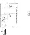
- FIG. 3is a block diagram of one embodiment of the configurable coupling circuit 46.
- the configurable coupling circuit 46includes a capacitor C1 60, an inductor L1 62, and a second capacitor C2 66.
- the configurable coupling circuitincludes a switch 64.
- the switch 64in this embodiment connects the antenna section 48 and capacitor 66 to the inductor L1 and capacitor C1 in a first position. In a second position, the switch 64 connects the antenna section 48 and capacitor 66 to ground or otherwise isolates the antenna from the inductor L1 and capacitor C1.
- the switch 64may be an actuator, a transistor circuit, or other equivalent device. For an active tag, a battery 41 may power the switch 64.
- an RFID reader 16-18transmits a continuous wave, unmodulated signal to power the multi-mode RFID tag 38.
- the multi-mode RFID tag 38may then use voltage generated from the power generating and signal detection module 40 to power the switch 64 to change positions.
- the multi-mode RFID tag 38may be configured prior to provisioning to operate in only near field mode or far field mode.
- the multi-mode RFID tag 38may be hardwired at manufacturing to only couple to the antenna section 48 for operation in far field mode or to only couple to the coil antenna 62 to operate in near field mode.
- the RFID tag 38may be pre-programmed to operate only in near field mode or far field mode prior to provisioning.
- the antenna 48 and capacitor C2are coupled to inductor L1 and capacitor C1.
- Inductor L1 and capacitor C1are operable as an impedance matching circuit for the antenna 48.
- the inductor L1provides an inductance value for impedance matching for the antenna 48 and the capacitor C1 provides a capacitance value to the impedance matching for the antenna 48.
- the capacitor C1is adjustable or variable, such as a digital switched capacitor, and is operable to be tuned to provide a desired capacitance value for the impedance matching in far field mode.
- the antenna 48 and the configurable coupling circuit 46receive the inbound receive signal 50 and are operable to provide the inbound receive signal 50 to the power generating and signal detection module 40.
- the switch 64is open such that the capacitor C2 is floating or connected to ground.
- the multi-mode RFID tag 38does not include a switch 64 but is hardwired at manufacturing to isolate the antenna 48 and/or capacitor C2 from the inductor L1.
- other devices other than a switch 64may be used to isolate the antenna 48 and/or capacitor C2 and the inductor L1 while the multi-mode RFID tag 38 is in near field mode.
- the inductor L1acts as a coil antenna to provide electromagnetic or inductive coupling with the coil or coils of RFID reader 14-18.
- the inductor L1 and the capacitor C1form a resonant circuit tuned to the transmission frequency of the RFID reader 14-18.
- the voltage at the inductor L1reaches a maximum due to resonance step-up in the parallel resonant circuit.
- the capacitor C1is adjustable or variable and is operable to be tuned to provide optimization of the parallel resonant circuit.
- the capacitor C1may be adjusted to provide optimization of at least one of bandwidth, quality factor, gain and roll-off of the configurable coupling circuit 46 in the near field mode.
- the distance between the inductor L1 of the RFID tag 38 and the coil antenna of the RFID reader 14-18must not exceed approximately ⁇ /2 ⁇ , so that the inductor L1 is located within the magnetic field created by the coil antenna of the RFID reader 14-18.
- the configurable coupling circuit 46is operable to provide the inbound receive signal 50 to the power generating and signal detection module 40.
- the inductor L1acts as a coiled antenna that creates the magnetic field from current flowing through the inductor L1 using the energy provided to the transmit section 44 by the power generating and signal detection module 40.
- the distance between the inductor L1 of the RFID tag 38 and the coil antenna of the RFID reader 14-18should be equal to or less than approximately ⁇ /2 ⁇ , so that the coil antenna of the RFID reader 14-18 is located within the magnetic field created by the inductor L1.
- the baseband processing module 42is operable to process commands from an RFID reader 14-18.
- one command from the RFID reader 14-18may be a mode command to operate the multi-mode RFID tag 38 in near field mode or in far field mode.
- the baseband processing module 42is operable to configure the multi-mode RFID tag 38 to operate in near field more or far field mode.
- the multi-mode RFID tagmay have a preset input that may be set by a user to determine the mode of operation. Thus, upon installation of the multi-mode RFID tag in a particular application, the RFID tag may be preset to the mode best suited for such application.
- FIG 4illustrates another embodiment of a multi-mode RFID tag 68 in accordance with the present invention.
- the multi-mode RFID tag 68 in this embodimentincludes a power generating and signal detection module 40, a baseband processing module 42, a transmit section 44, a configurable coupling circuit 46, and an antenna section 48.
- a switch 70 and load resistance Zmare connected between the transmit section and configurable coupling circuit.
- the switching on and off of the load resistance Zm at the inductor LIe.g. the coil antenna in the near field mode, effects voltage changes at the RFID reader's coil antenna and thus has the effect of an amplitude modulation of the RFID reader's antenna voltage by the multi-mode RFID tag 38.
- the transmit section 44By switching on and off of the load resistance Zm in response to the outbound encoded data 54, the transmit section 44 is operable to transfer the data from the RFID tag to the RFID reader with load modulation. Similarly, the switch 70 and load resistance Zm can modulate the RF backscatter signal from the transmit section 44 to modulate the reflected RF outbound transmit signal 56 in far field mode. Thus, the switch 70 and load resistance Zm provide an efficient modulation of the outbound transmit signal 56 for the multi-mode RFID tag 38.
- the embodiment 4illustrates a passive RFID multi-mode tag 38.
- the multi-mode tag 38may also be designed as an active tag by including a battery 41 to provide the power to operate the RFID tag 38.
- the power generating circuitmay not be necessary and an RFID reader 14-18 does not need to transmit a CW, unmodulated signal to power the RFID tag 38 before communicating with the RFID tag 38.
- the battery 41would allow the RFID tag 38 to switch between near field mode and far field mode in order to detect signals from an RFID reader 14-18 without waiting for a power signal and command from an RFID reader 14-18.
- the disadvantage of active tags with a batteryis the shorter duration of life of the tag. The tag would become inoperable when the battery loses its charge.
- an active multi-mode RFID tag 38may be optimal for higher processing applications or applications that only need certain duration, e.g. tags for perishable items.
- FIG. 5illustrates a schematic block diagram of the inductor L1 62 in one embodiment of the multimode RFID tag 38 in accordance with the present invention.
- the inductor L1 in the configurable coupling circuit 46operates in the ultra high frequency (e.g., UHF) range in near field mode. Due to higher frequencies, the coils of the inductor L1 can be much smaller sized coils and can be integrated on chip with other modules of the multi-mode RFID tag 38.
- the inductor L1 62has a radius r 2 ; the coil antenna 80 of the RFID reader 14-18 has a radius r 1 ; and the distance between the inductor L1 and the coil antenna 80 equals distance d.
- L tagequals approximately 56.6nH
- Q tagequals approximately 4.9.
- Figure 6illustrates the range between the RFID tag 38 and the RFID reader 14-18 in the UHF near field mode assuming the embodiment of Figure 5 .
- the rangeis limited by the transmit power of the tag.
- a Manchester coding with data rate of 50kbpsis utilized in this embodiment.
- UHF near field RFID communicationsare well suited for near read applications, such as inventory items, monitory paper authentication, passports, credit cards, etc.
- the near field UHF operation of the RFID tag 38also has more efficient operation near fluids, such as fluid medication bottles.
- the inductor L1 or coil antenna 62may be designed sufficiently small to be integrated on chip.
- the multi-mode RFID tag 38thus provides near field and far field mode operation.
- the multi-mode RFID tagoperates in UHF range in the near field mode with an integrated on chip inductor or coil antenna.
- the RFID tagprovides multi-standard, multi-technology option for use in multiple applications.
- the RFID tagsare not limited to only near read or far read applications but can be used in both type applications and are operable to be switched from near field mode to far field mode or from far field mode to near field mode to accommodate different types of RFID readers and differing distances between the multi-mode RFID tag and an RFID reader.
- the terms “substantially” and “approximately”provides an industry-accepted tolerance for its corresponding term and/or relativity between items. Such an industry-accepted tolerance ranges from less than one percent to fifty percent and corresponds to, but is not limited to, component values, integrated circuit process variations, temperature variations, rise and fall times, and/or thermal noise. Such relativity between items ranges from a difference of a few percent to magnitude differences.
- the term(s) "coupled to” and/or “coupling” and/orincludes direct coupling between items and/or indirect coupling between items via an intervening item (e.g., an item includes, but is not limited to, a component, an element, a circuit, and/or a module) where, for indirect coupling, the intervening item does not modify the information of a signal but may adjust its current level, voltage level, and/or power level.
- an intervening iteme.g., an item includes, but is not limited to, a component, an element, a circuit, and/or a module
- inferred couplingi.e., where one element is coupled to another element by inference
- the term "operable to”indicates that an item includes one or more of power connections, input(s), output(s), etc., to perform one or more its corresponding functions and may further include inferred coupling to one or more other items.
- the term “associated with”,includes direct and/or indirect coupling of separate items and/or one item being embedded within another item.
- the term “compares favorably”,indicates that a comparison between two or more items, signals, etc., provides a desired relationship. For example, when the desired relationship is that signal 1 has a greater magnitude than signal 2, a favorable comparison may be achieved when the magnitude of signal 1 is greater than that of signal 2 or when the magnitude of signal 2 is less than that of signal 1.
Landscapes
- Engineering & Computer Science (AREA)
- Physics & Mathematics (AREA)
- General Physics & Mathematics (AREA)
- Theoretical Computer Science (AREA)
- Computer Networks & Wireless Communication (AREA)
- Computer Hardware Design (AREA)
- Microelectronics & Electronic Packaging (AREA)
- Signal Processing (AREA)
- Computer Vision & Pattern Recognition (AREA)
- Artificial Intelligence (AREA)
- Health & Medical Sciences (AREA)
- Toxicology (AREA)
- Electromagnetism (AREA)
- General Health & Medical Sciences (AREA)
- Computer Security & Cryptography (AREA)
- General Engineering & Computer Science (AREA)
- Near-Field Transmission Systems (AREA)
Description
- This invention relates generally to communication systems and more particularly to RFID systems.
- A radio frequency identification (RFID) system generally includes a reader, also known as an interrogator, and a remote tag, also known as a transponder. Each tag stores identification or other data for use in identifying a person, item, pallet or other object or data related to a characteristic of a person, item, pallet or other object. RFID systems may use active tags that include an internal power source, such as a battery, and/or passive tags that do not contain an internal power source, but instead are remotely powered by the reader.
- Communication between the reader and the remote tag is enabled by radio frequency (RF) signals. In general, to access the identification data stored on an RFID tag, the RFID reader generates a modulated RF interrogation signal designed to evoke a modulated RF response from a tag. The RF response from the tag includes the coded data stored in the RFID tag. The RFID reader decodes the coded data to identify or determine the characteristics of a person, item, pallet or other object associated with the RFID tag. For passive tags without a battery or other power source, the RFID reader also generates an unmodulated, continuous wave (CW) signal to activate and power the tag during data transfer. Thus, passive tags obtain power from transmissions of the RFID reader. Active tags include a battery and have greater ability to power transceivers, processer, memory and other on-tag devices.
- RFID systems typically employ either far field or near field technology. In far field technology, the distance between the reader and the tag is great compared to the wavelength of the carrier signal. Typically, far field technology uses carrier signals in the ultra high frequency or microwave frequency ranges. In far-field applications, the RFID reader generates and transmits an RF signal via an antenna to all tags within range of the antenna. One or more of the tags that receive the RF signal responds to the reader using a backscattering technique in which the tags modulate and reflect the received RF signal.
- In near-field technology, the operating distance is usually less than one wavelength of the carrier signal. Thus, the reading range is approximately limited to 20 cm or less depending on the frequency. In near field applications, the RFID reader and tag communicate via electromagnetic or inductive coupling between the coils of the reader and the tag. Typically, the near field technology uses carrier signals in the low frequency range. For the tag coil antennas, RFID tags have used a multilayer coil (e.g., 3 layers of 100-150 turns each) wrapped around a metal core at lower frequencies of 135 KHz. Sometimes, at higher frequency of 13.56 MHz, RFID tags have used a planar spiral coil inductor with 5-7 turns over a credit-card-sized form factor. Such tag coil antennas are large in comparison to the other modules of the RFID tag and are not able to be integrated on a chip, such as a complementary metal-oxide-semiconductor (CMOS), bipolar complementary metal-oxide-semiconductor (BiCMOS) or gallium arsenide (GaAs) integrated circuit, with other modules of the RFID tag.
- The International Organization for Standardization (ISO) has developed an RFID standard called the ISO 18000 series. The ISO 18000 series standard describes air interface protocols for RFID systems especially in applications used to track items in a supply chain. The ISO 18000 series has seven parts to cover the major frequencies used in RFID systems around the world. The seven parts are:
- 18000-1: Generic parameters for air interfaces for globally accepted frequencies;
- 18000-2: Air interface for below 135 KHz;
- 18000-3: Air interface for 13.56 MHz;
- 18000-4: Air interface for 2.45 GHz;
- 18000-5: Air interface for 5.8 GHz;
- 18000-6: Air interface for 860 MHz to 930 MHz;
- 18000-7: Air interface at 433.92 MHz.
- According to the ISO 18000-2 and 18000-3 parts of the ISO 18000 series, near-field technology with magnetic/inductive coupling has an air interface protocol at low frequency (LF) of 135 KHz or less or at 13.56 high frequency (HF). ISO 18000-3 defines two modes. In mode 1, the tag to reader data rate is 26.48 kbps while mode 2 is a high speed interface of 105.9375 kbps on each of 8 channels. The communication protocol used by the reader and the tag is typically a load modulation technique.
- Far field technology with RF backscatter coupling has three ISO defined air interfaces at 2.45 GHz microwave frequency according to ISO 18000-5, 860MHZ to 930 MHz ultra high frequency (UHF) range according to ISO 18000-6 and 433.92 MHz UHF according to ISO 18000-7. For UHF at 860-930 MHz, the ISO 18000-6 has defined two tag types, Type A and Type B with a tag to reader link defined as including 40kbps data rate, Amplitude Shift Keying (ASK) modulation, and biphase-space or FM0 encoding of data.
- In addition, the EPCglobal Class 1, Generation 2 standard defines a tag standard using UHF with a tag to reader link of 40 to 640 kbps, ASK or Phase Shift Keying (PSK) modulation and data encoding of FMO or Miller-modulated subcarrier.
- Generally, tags employing near field technology operating at LF or HF have been used in applications involving item-level tagging for inventory control in the supply chain management or applications involving short range reads such as smart cards or vicinity credit cards, e.g. for access control or monetary use, passports, money bills authentication, bank documents, etc. Such applications do not need long range reads of the tags but may need more security provided by near field technology. In addition, near field technology is known for better performance on tags near fluids, such as fluid medications, wherein far field RF coupling tends to incur interference from the fluids.
- Tags employing far field technology RF coupling at microwave or UHF have been used in applications involving shipping units such as pallets or carton level tracking or other applications needing long-distance reads.
- These different types of technology and the number of different RFID standards, each defining a different protocol for enabling communication between the reader and the tag, has inhibited the wide spread use of RFID tags for multiple applications. Therefore, a need exists for a highly integrated, low-cost RFID tag. In addition, a need exists for a multi-standard, multi-technology RFID tag.
US 2005/052283 A1 describes a multi-mode RFID which has different tuning circuits for tuning to low and high frequencies.- The present invention relates to a multi-mode radio frequency identification (RFID) tag according to claim 1 and a method for operating a multi-mode RFID tag according to
claim 12. Preferred embodiments are described in the dependent claims. Figure 1 is a schematic block diagram of an embodiment of an RFID system in accordance with the present invention;Figure 2 is a schematic block diagram of an embodiment of a multi-mode RFID tag in accordance with the present invention;Figure 3 is a schematic block diagram of a configurable coupling circuit in one embodiment of a multimode RFID tag in accordance with the present invention;Figure 4 is a schematic block diagram of another embodiment of a multimode RFID tag in accordance with the present invention;Figure 5 is a schematic block diagram of coil antennas in one embodiment of a multimode RFID tag and RFID reader in accordance with the present invention; andFigure 6 is a schematic block diagram of magnetic coupling between a multi-mode RFID tag and RFID reader in one embodiment in accordance with the present invention.Figure 1 is a schematic block diagram of an RFID (radio frequency identification) system that includes a computer/server 12, a plurality of RFID readers 14-18 and a plurality of RFID tags 20-30. The RFID tags 20-30 may each be associated with a particular object for a variety of purposes including, but not limited to, tracking inventory, tracking status, location determination, assembly progress, et cetera. The RFID tags may be active devices that include internal power sources or passive devices that derive power from the RFID readers 14-18.- Each RFID reader 14-18 wirelessly communicates with one or more RFID tags 20 - 30 within its coverage area. For example, RFID tags 20 and 22 may be within the coverage area of
RFID reader 14, RFID tags 24 and 26 may be within the coverage area ofRFID reader 16, andRFID tags RFID reader 18. In one mode of operation, the RF communication scheme between the RFID readers 14-18 and RFID tags 20-30 is a backscatter coupling technique using far field technology whereby the RFID readers 14 - 18 request data from the RFID tags 20-30 via an RF signal, and the RF tags 20-30 respond with the requested data by modulating and backscattering the RF signal provided by the RFID readers 14-18. In another mode of operation, the RF communication scheme between the RFID readers 14-18 and RFID tags 20-30 is a magnetic or inductive coupling technique using near field technology whereby the RFID readers 14-18 magnetically or inductively couple to the RFID tags 20-30 to access the data on the RFID tags 20-30. Thus, in one embodiment of the current invention, the RFID tags 20-30 may communicate in a far field mode to an RFID reader 14-18 with such capabilities and in a near field mode to an RFID reader 14-18 with such capabilities. - The RFID readers 14-18 collect data as may be requested from the computer/
server 12 from each of the RFID tags 20-30 within its coverage area. The collected data is then conveyed to computer/server 12 via the wired orwireless connection 32 and/or via peer-to-peer communication 34. In addition, and/or in the alternative, the computer/server 12 may provide data to one or more of the RFID tags 20-30 via the associated RFID reader 14-18. Such downloaded information is application dependent and may vary greatly. Upon receiving the downloaded data, the RFID tag 20-30 can store the data in a non-volatile memory therein. - As indicated above, the RFID readers 14-18 may optionally communicate on a peer-to-peer basis such that each RFID reader does not need a separate wired or
wireless connection 32 to the computer/server 12. For example,RFID reader 14 andRFID reader 16 may communicate on a peer-to-peer basis utilizing a back scatter technique, a wireless LAN technique, and/or any other wireless communication technique. In this instance,RFID reader 16 may not include a wired orwireless connection 32 to computer/server 12. In embodiments in which communications betweenRFID reader 16 and computer/server 12 are conveyed through the wired orwireless connection 32, the wired orwireless connection 32 may utilize any one of a plurality of wired standards (e.g., Ethernet, fire wire, et cetera) and/or wireless communication standards (e.g., IEEE 802.1 lx, Bluetooth, et cetera). - As one of ordinary skill in the art will appreciate, the RFID system of
Figure 1 may be expanded to include a multitude of RFID readers 14-18 distributed throughout a desired location (for example, a building, office site, et cetera) where the RFID tags may be associated with access cards, smart cards, mobile phones, personal digital assistants, laptops, personal computers, inventory items, pallets, cartons, equipment, personnel, et cetera. In addition, it should be noted that the computer/server 12 may be coupled to another server and/or network connection to provide wide area network coverage. Figure 2 is a schematic block diagram of an embodiment of amulti-mode RFID tag 38 which can be used as one of the RFID tags 20-30 inFigure 1 . Themulti-mode RFID tag 38 is operable to communicate in a far field mode to an RFID reader 14-18 and in a near field mode to an RFID reader 14-18. Themulti-mode RFID tag 38 includes a power generating andsignal detection module 40, abaseband processing module 42, a transmitsection 44, aconfigurable coupling circuit 46, and anantenna section 48. Themulti-mode RFID tag 38 may be an active tag and include abattery 41. If an active tag, thebattery 41 may replace or assist the power generating function of the power generating andsignal detection module 40 to power thebaseband processing module 42, transmitsection 44 andconfigurable coupling circuit 46. If themulti-mode RFID tag 38 is a passive tag, nobattery 41 is present.- The power generating and
signal detection module 40,baseband processing module 42 and transmitsection 44 may be a single processing device or a plurality of processing devices. Such a processing device may be a microprocessor, micro-controller, digital signal processor, microcomputer, central processing unit, field programmable gate array, programmable logic device, state machine, logic circuitry, analog circuitry, digital circuitry, and/or any device that manipulates signals (analog and/or digital) based on hard coding of the circuitry and/or operational instructions. One or more of the modules may have an associated memory element, which may be a single memory device, a plurality of memory devices, and/or embedded circuitry of the module. Such a memory device may be a read-only memory, random access memory, volatile memory, non-volatile memory, static memory, dynamic memory, flash memory, cache memory, and/or any device that stores digital information. Note that when the module implements one or more of its functions via a state machine, analog circuitry, digital circuitry, and/or logic circuitry, the memory element storing the corresponding operational instructions may be embedded within, or external to, the circuitry comprising the state machine, analog circuitry, digital circuitry, and/or logic circuitry. Further note that, the memory element stores, and the module executes, hard coded and/or operational instructions corresponding to at least some of the steps and/or functions illustrated inFigures 1-7 . - In an embodiment, the
antenna section 48 is a dipole type antenna operable at microwave or UHF ranges. Folded dipoles or half-wave dipoles can be used or other dipole type antennas that can be bent or meandered with capacitive tip-loading or bowtie-like broadband structures are also used for compact applications. In general, theantenna section 48 can be one of several types of antennas optimized for the desired frequency of operation and application. - In operation, the
configurable coupling circuit 46 is operable to couple the power generating andsignal detection module 40 to theantenna section 48 in a far field mode or to couple the power generating andsignal detection module 40 to an inductor or coil antenna in theconfigurable coupling circuit 46 in a near field mode, as explained in more detail below. In either mode, theconfigurable coupling circuit 46 is operable to transmit an inbound receivesignal 50 to the power generating andsignal detection module 40. In a passive embodiment ofmultimode RFID tag 38, the RFID reader 14-18 first generates an unmodulated, continuous wave (CW) signal to activate and power the tag. The power generating andsignal detection module 40 converts this type of CW unmodulated inbound receivesignal 50 into a supply voltage. The power generating circuitsignal detection module 40 stores the supply voltage and provides it to the other modules for operation. - The RFID reader 14-18 then transmits a modulated, encoded interrogation inbound receive
signal 50. The power generating andsignal detection module 40 receives the inbound receivesignal 50 from theconfigurable coupling circuit 46. The power generating andsignal detection module 40 demodulates the inbound receivesignal 50 to recover the encodeddata 52. Depending on the RFID reader 14-18 and mode of operation, the inbound receivesignal 50 may be modulated using Amplitude Shift Keying (ASK) or Phase Shift Keying (PSK) or other type of modulation. In an embodiment, the power generating andsignal detection module 40 is operable to demodulate the inbound receivesignal 50 using one or more types of demodulation techniques to recover the encodeddata 52 from the inbound receivesignal 50. The power generating andsignal detection module 40 transmits the recovered encodeddata 52 to thebaseband processing module 42. - The
baseband processing module 42 receives the encodeddata 52 and decodes the encodeddata 52 using one or more protocols. Different data encoding protocols may be defined for signals in near field mode and signals in far field mode. For example, in near field mode, a first data encoding protocol may be used by thebaseband processing module 42 for decoding data while a second data encoding protocol may be used by thebaseband processing module 42 for decoding data in far field mode. For instance, Manchester encoding may be used when in near field mode and Miller-modulated subcarrier coding and/or biphase-space encoding may be used when in the far field mode. Alternatively, thebaseband processing module 42 may use the same data encoding protocol for near field mode and far field mode. - In an embodiment, the
baseband processing module 42 is programmed with multiple encoding protocols to be operable to decode the encodeddata 52 in accordance with different protocols. Thus, thebaseband processing module 42 is operable to decode the encodeddata 52 using different encoding protocols when necessary in either near field or far field mode. For example, when operating in near field mode, thebaseband processing module 42 may attempt to decode the encodeddata 52 using a first protocol typical in near field operations, such as Manchester coding. If such decoding is unsuccessful, the baseband processing module is operable to attempt decoding the encodeddata 52 with a next protocol until the encodeddata 52 is decoded. Similarly, when operating in far field mode, thebaseband processing module 42 may attempt to decode the encodeddata 52 using a second protocol typical in far field operations, such as Miller-modulated subcarrier coding and biphase-space encoding. If such decoding is unsuccessful, the baseband processing module is operable to attempt decoding the encodeddata 52 with a next protocol until the encoded data is decoded. - Once decoded, the
baseband processing module 42 processes the decoded data to determine a command or commands contained therein. The command may be to store data, update data, reply with stored data, verify command compliance, acknowledgement, change mode of operation, etc. If the command(s) requires a response, thebaseband processing module 42 determines the response data and encodes the response data into outbound encodeddata 54. Preferably, thebaseband processing module 42 encodes the data for the response using the same encoding protocol used to decode the inbound encodeddata 52. Once encoded, thebaseband processing module 42 provides the outbound encodeddata 54 to the transmitsection 44. The transmitsection 44 receives the outbound encodeddata 54 and converts the outbound encodeddata 54 into an outbound transmitsignal 56. - The outbound transmit
signal 56 is a carrier signal with amplitude modulation, such as ASK, or phase modulation, such as PSK, or load modulation of the carrier signal can be used. The frequency of the carrier signal in near field mode in one embodiment is a low frequency (LF) or a high frequency (HF) range. In accordance with ISO series standards, such near field ranges are a low frequency at approximately 135 KHz or less and a high frequency at approximately at 13.56 MHz. In far field mode, in an embodiment, the frequency of the carrier signal is in the ultra high frequency range or microwave range. In accordance with ISO series standards, such far field ranges are at approximately 2.45 GHz frequency, approximately 860 MHZ to 930 MHz ultra high frequency (UHF) range or approximately 433.92 MHz UHF. - In near field mode, the
configurable coupling circuit 46 is operable to couple the transmitsection 44 to an inductor in theconfigurable coupling circuit 46 to transmit the outbound transmitsignal 56 using electromagnetic or inductive coupling to an RFID reader 16-18. In far field mode, theconfigurable coupling circuit 46 is operable to couple the transmitsection 44 to theantenna section 48, and themulti-mode RFID tag 38 then utilizes a backscattering RF technology to transmit the outbound transmitsignal 56 to RFID readers 16-18. Figure 3 is a block diagram of one embodiment of theconfigurable coupling circuit 46. Theconfigurable coupling circuit 46 includes acapacitor C1 60, aninductor L1 62, and asecond capacitor C2 66. In one embodiment, the configurable coupling circuit includes aswitch 64. Theswitch 64 in this embodiment connects theantenna section 48 andcapacitor 66 to the inductor L1 and capacitor C1 in a first position. In a second position, theswitch 64 connects theantenna section 48 andcapacitor 66 to ground or otherwise isolates the antenna from the inductor L1 and capacitor C1. Theswitch 64 may be an actuator, a transistor circuit, or other equivalent device. For an active tag, abattery 41 may power theswitch 64. For passive tags, an RFID reader 16-18 transmits a continuous wave, unmodulated signal to power themulti-mode RFID tag 38. Themulti-mode RFID tag 38 may then use voltage generated from the power generating andsignal detection module 40 to power theswitch 64 to change positions. In an alternate embodiment, themulti-mode RFID tag 38 may be configured prior to provisioning to operate in only near field mode or far field mode. For example, themulti-mode RFID tag 38 may be hardwired at manufacturing to only couple to theantenna section 48 for operation in far field mode or to only couple to thecoil antenna 62 to operate in near field mode. In another example, theRFID tag 38 may be pre-programmed to operate only in near field mode or far field mode prior to provisioning.- In far field mode, the
antenna 48 and capacitor C2 are coupled to inductor L1 and capacitor C1. Inductor L1 and capacitor C1 are operable as an impedance matching circuit for theantenna 48. The inductor L1 provides an inductance value for impedance matching for theantenna 48 and the capacitor C1 provides a capacitance value to the impedance matching for theantenna 48. In an embodiment, the capacitor C1 is adjustable or variable, such as a digital switched capacitor, and is operable to be tuned to provide a desired capacitance value for the impedance matching in far field mode. Thus, in far field mode, theantenna 48 and theconfigurable coupling circuit 46 receive the inbound receivesignal 50 and are operable to provide the inbound receivesignal 50 to the power generating andsignal detection module 40. - In near field mode, the
switch 64 is open such that the capacitor C2 is floating or connected to ground. In another embodiment, themulti-mode RFID tag 38 does not include aswitch 64 but is hardwired at manufacturing to isolate theantenna 48 and/or capacitor C2 from the inductor L1. In an alternate embodiment, other devices other than aswitch 64 may be used to isolate theantenna 48 and/or capacitor C2 and the inductor L1 while themulti-mode RFID tag 38 is in near field mode. - The inductor L1 acts as a coil antenna to provide electromagnetic or inductive coupling with the coil or coils of RFID reader 14-18. The inductor L1 and the capacitor C1 form a resonant circuit tuned to the transmission frequency of the RFID reader 14-18. In response to the magnetic field generated by the RFID reader 14-18 coil antenna, the voltage at the inductor L1 reaches a maximum due to resonance step-up in the parallel resonant circuit. In an embodiment, the capacitor C1 is adjustable or variable and is operable to be tuned to provide optimization of the parallel resonant circuit. For example, the capacitor C1 may be adjusted to provide optimization of at least one of bandwidth, quality factor, gain and roll-off of the
configurable coupling circuit 46 in the near field mode. Generally, to operate in the near field mode, the distance between the inductor L1 of theRFID tag 38 and the coil antenna of the RFID reader 14-18 must not exceed approximately λ/2π, so that the inductor L1 is located within the magnetic field created by the coil antenna of the RFID reader 14-18. In near field mode, theconfigurable coupling circuit 46 is operable to provide the inbound receivesignal 50 to the power generating andsignal detection module 40. - During transmission, the inductor L1 acts as a coiled antenna that creates the magnetic field from current flowing through the inductor L1 using the energy provided to the transmit
section 44 by the power generating andsignal detection module 40. Again, in order to receive the outbound transmitsignal 56 in the near field mode, the distance between the inductor L1 of theRFID tag 38 and the coil antenna of the RFID reader 14-18 should be equal to or less than approximately λ/2π, so that the coil antenna of the RFID reader 14-18 is located within the magnetic field created by the inductor L1. - In one embodiment, as explained above with respect to
Figure 2 , thebaseband processing module 42 is operable to process commands from an RFID reader 14-18. For example, one command from the RFID reader 14-18 may be a mode command to operate themulti-mode RFID tag 38 in near field mode or in far field mode. Upon processing such mode command, thebaseband processing module 42 is operable to configure themulti-mode RFID tag 38 to operate in near field more or far field mode. In another embodiment, the multi-mode RFID tag may have a preset input that may be set by a user to determine the mode of operation. Thus, upon installation of the multi-mode RFID tag in a particular application, the RFID tag may be preset to the mode best suited for such application. Figure 4 illustrates another embodiment of amulti-mode RFID tag 68 in accordance with the present invention. Similarly, toFigures 2 and3 , themulti-mode RFID tag 68 in this embodiment includes a power generating andsignal detection module 40, abaseband processing module 42, a transmitsection 44, aconfigurable coupling circuit 46, and anantenna section 48. In addition, aswitch 70 and load resistance Zm are connected between the transmit section and configurable coupling circuit. In operation, the switching on and off of the load resistance Zm at the inductor LI, e.g. the coil antenna in the near field mode, effects voltage changes at the RFID reader's coil antenna and thus has the effect of an amplitude modulation of the RFID reader's antenna voltage by themulti-mode RFID tag 38. By switching on and off of the load resistance Zm in response to the outbound encodeddata 54, the transmitsection 44 is operable to transfer the data from the RFID tag to the RFID reader with load modulation. Similarly, theswitch 70 and load resistance Zm can modulate the RF backscatter signal from the transmitsection 44 to modulate the reflected RF outbound transmitsignal 56 in far field mode. Thus, theswitch 70 and load resistance Zm provide an efficient modulation of the outbound transmitsignal 56 for themulti-mode RFID tag 38.- The
embodiment 4 illustrates a passive RFIDmulti-mode tag 38. In another embodiment shown inFigure 2 , themulti-mode tag 38 may also be designed as an active tag by including abattery 41 to provide the power to operate theRFID tag 38. With active tag design, the power generating circuit may not be necessary and an RFID reader 14-18 does not need to transmit a CW, unmodulated signal to power theRFID tag 38 before communicating with theRFID tag 38. In addition, thebattery 41 would allow theRFID tag 38 to switch between near field mode and far field mode in order to detect signals from an RFID reader 14-18 without waiting for a power signal and command from an RFID reader 14-18. The disadvantage of active tags with a battery is the shorter duration of life of the tag. The tag would become inoperable when the battery loses its charge. However, an activemulti-mode RFID tag 38 may be optimal for higher processing applications or applications that only need certain duration, e.g. tags for perishable items. Figure 5 illustrates a schematic block diagram of theinductor L1 62 in one embodiment of themultimode RFID tag 38 in accordance with the present invention. In this embodiment, the inductor L1 in theconfigurable coupling circuit 46 operates in the ultra high frequency (e.g., UHF) range in near field mode. Due to higher frequencies, the coils of the inductor L1 can be much smaller sized coils and can be integrated on chip with other modules of themulti-mode RFID tag 38. As shown inFigure 5 , theinductor L1 62 has a radius r2; thecoil antenna 80 of the RFID reader 14-18 has a radius r1; and the distance between the inductor L1 and thecoil antenna 80 equals distance d. In this embodiment, with reference toFigure 5 , the magnetic field M12 between thecoil antenna 80 of the RFID reader 14-18 and the inductor L1 of theRFID tag 38 is:


multi-mode RFID tag 38 operating in near field mode in UHF range at approximately 900 MHz, the Ltag equals approximately 56.6nH and Qtag equals approximately 4.9.Figure 6 illustrates the range between theRFID tag 38 and the RFID reader 14-18 in the UHF near field mode assuming the embodiment ofFigure 5 . As seen inFigure 6 , the range is limited by the transmit power of the tag. For example:

- Though the range of communication is smaller (e.g., < 5mm) in UHF near field mode than at lower frequencies (such as HF and LF), such short range, UHF near field RFID communications are well suited for near read applications, such as inventory items, monitory paper authentication, passports, credit cards, etc. The near field UHF operation of the
RFID tag 38 also has more efficient operation near fluids, such as fluid medication bottles. In addition, the inductor L1 orcoil antenna 62 may be designed sufficiently small to be integrated on chip. By integrating theRFID tag 38 onto a single integrated circuit, the cost of theRFID tag 38 can be significantly reduced. - The
multi-mode RFID tag 38 thus provides near field and far field mode operation. In one embodiment the multi-mode RFID tag operates in UHF range in the near field mode with an integrated on chip inductor or coil antenna. By operating in both near field and far field mode, the RFID tag provides multi-standard, multi-technology option for use in multiple applications. As such, the RFID tags are not limited to only near read or far read applications but can be used in both type applications and are operable to be switched from near field mode to far field mode or from far field mode to near field mode to accommodate different types of RFID readers and differing distances between the multi-mode RFID tag and an RFID reader. - As may be used herein, the terms "substantially" and "approximately" provides an industry-accepted tolerance for its corresponding term and/or relativity between items. Such an industry-accepted tolerance ranges from less than one percent to fifty percent and corresponds to, but is not limited to, component values, integrated circuit process variations, temperature variations, rise and fall times, and/or thermal noise. Such relativity between items ranges from a difference of a few percent to magnitude differences. As may also be used herein, the term(s) "coupled to" and/or "coupling" and/or includes direct coupling between items and/or indirect coupling between items via an intervening item (e.g., an item includes, but is not limited to, a component, an element, a circuit, and/or a module) where, for indirect coupling, the intervening item does not modify the information of a signal but may adjust its current level, voltage level, and/or power level. As may further be used herein, inferred coupling (i.e., where one element is coupled to another element by inference) includes direct and indirect coupling between two items in the same manner as "coupled to". As may even further be used herein, the term "operable to" indicates that an item includes one or more of power connections, input(s), output(s), etc., to perform one or more its corresponding functions and may further include inferred coupling to one or more other items. As may still further be used herein, the term "associated with", includes direct and/or indirect coupling of separate items and/or one item being embedded within another item. As may be used herein, the term "compares favorably", indicates that a comparison between two or more items, signals, etc., provides a desired relationship. For example, when the desired relationship is that signal 1 has a greater magnitude than signal 2, a favorable comparison may be achieved when the magnitude of signal 1 is greater than that of signal 2 or when the magnitude of signal 2 is less than that of signal 1.


Claims (15)
- A multi-mode radio frequency identification (RFID) tag (20, 22, 24, 26, 28, 30, 38, 68) comprises:a configurable coupling circuit (46) that, when the multi-mode RFID tag is in a far field mode, provides electromagnetic coupling to an RFID reader (14, 16, 18) via an antenna (48) and, when the multi-mode RFID tag is in a near field mode, provides radio frequency (RF) coupling to the RFID reader (14, 16, 18) via an inductor (62), the coupling circuit (46) acting as an impedance circuit for the antenna (48), wherein the inductor (62) provides the electromagnetic coupling in the near field mode and an inductance value for impedance matching in the far field mode;a power generating and signal detection module (40) coupled to the configurable coupling circuit (46), wherein the power generating and signal detection module (40) converts an inbound receive signal into a supply voltage and recovers encoded data from the inbound receive signal;a baseband processing module (42) coupled to:decode the encoded data to produce a decoded signal;process the decoded signal;when the processing of the decoded signal indicates generating a response signal, generate the response signal; andencode the response signal to produce outbound encoded data; anda transmit section (44) coupled to the configurable coupling circuit (46), wherein the transmit section (44) converts the outbound encoded data into an outbound transmit signal.
- The multi-mode RFID tag of claim 1, wherein the configurable coupling circuit (46) further comprises:a first capacitor (66) coupled to the antenna (48) in the far field mode and open or coupled to ground in the near field mode; anda second capacitor (60) coupled to the inductor (62) to provide a capacitance value to tune the impedance matching for the far field mode or to tune at least one of: bandwidth, quality factor, gain and roll-off of the configurable coupling circuit (46) in the near field mode.
- The multi-mode RFID tag of claim 2, wherein the second capacitor (60) is adjustable.
- The multi-mode RFID tag of claim 2 or 3, wherein the antenna (48) in the far field mode is operable to transmit and receive RF signals in an ultra high frequency (UHF) range.
- The multi-mode RFID tag of any of claims 2 to 4, wherein the inductor (62) to provide the electromagnetic coupling in the near field mode comprises a coil inductor operable to provide the electromagnetic coupling in ultra high frequency (UHF) range in the near field mode.
- The multi-mode RFID tag of any preceding claim, wherein the baseband processing module (42) that is coupled to decode the encoded data to produce a decoded signal, further functions to:utilize a first encoding/decoding protocol when in the near field mode; andutilize a second encoding/decoding protocol when in the far field mode.
- The multi-mode RFID tag of claim 6, wherein the baseband processing module (42) coupled to encode the response signal to produce encoded data, comprises:
at least a first encoding processing module for encoding the response signal in near field mode in the first encoding protocol and for encoding the response signal in far field mode in the second encoding protocol. - The multi-mode RFID tag of any preceding claim, wherein the inductor (62) to provide the electromagnetic coupling in the near field mode comprises a coil inductor operable to provide the electromagnetic coupling in low frequency (LF) range in the near field mode.
- The multi-mode RFID tag of any preceding claim, wherein the configurable coupling circuit (46) is operable to switch to near field mode and provide electromagnetic coupling to the RFID reader (14, 16, 18) in response to a command from the RFID reader (14, 16, 18).
- The multi-mode RFID tag of any preceding claim, wherein the configurable coupling circuit (46) is operable to switch to far field mode and provide RF coupling to the RFID reader (14, 16, 18) in response to a command from the RFID reader (14, 16, 18).
- The multi-mode RFID tag of any preceding claim, wherein the configurable coupling circuit (46) is configured to operate in far field mode and provide RF coupling to the RFID reader (14, 16, 18) until it receives a command from the RFID reader (14, 16, 18) to switch to near field mode and provide electromagnetic coupling to the RFID reader (14, 16, 18).
- A method for operating a multi-mode RFID tag (20, 22, 24, 26, 28, 30, 38, 68), comprising:configuring a coupling circuit (46) of the multi-mode RFID tag to provide RF coupling via an antenna (48) to an RFID reader (14, 16, 18) in a far field mode and inductive coupling via an inductor (62) to the RFID reader (14, 16, 18) in a near field mode, the coupling circuit (46) acting as an impedance circuit for the antenna (48), wherein the inductor (62) provides the electromagnetic coupling in the near field mode and an inductance value for impedance matching in the far field mode;communicating with the RFID reader (14, 16, 18) in one of the far field mode and the near field mode;when a command is received from the RFID reader (14, 16, 18), configuring the coupling circuit (46) to provide the other one of the far field mode and the near field mode; andcommunicating with the RFID in the other one of the far field mode and the near field mode.
- The method of claim 12, wherein communicating with the RFID reader (14, 16, 18) comprises:receiving an inbound signal from the RFID reader (14, 16, 18), recovering an encoded data signal from the inbound signal;decoding the recovered encoded data signal, wherein the encoded data signal is encoded with a first encoding protocol;processing the decoded data signal;generating a response signal to the decoded data signal in response to a command in the decoded data signal that requires a response to the RFID reader (14, 16, 18);encoding the response signal with the first encoding protocol.
- The multi-mode RFID tag (20, 22, 24, 26, 28, 30, 38, 68) of claim 1, wherein the power generating and signal detection module (40) is further operable to:convert the inbound receive signal from the RFID reader (14, 16, 18) into the supply voltage; andrecover the encoded data from the inbound receive signal in the near field mode and in the far field mode to produce a recovered encoded data signal, and whereinthe baseband processing module (42) is further operable to:decode the recovered encoded data signal using a first protocol when in the far field mode and using a second protocol when in the near field mode to produce the decoded signal; andencode the response signal using the first protocol when in the far field mode and using the second protocol when in the near field mode to produce the outbound encoded data.
- The multi-mode RFID tag (20, 22, 24, 26, 28, 30, 38, 68) of claim 14, wherein the antenna is a radio frequency (RF) antenna (48) operable to provide RF coupling in the far field mode, wherein the inductor is a coil antenna (62) operable to provide electromagnetic coupling in the near field mode, and
the power generating and signal detection module (40) is coupled to the RF antenna (48) or to the coil antenna (62).
Priority Applications (1)
| Application Number | Priority Date | Filing Date | Title |
|---|---|---|---|
| EP15001920.6AEP2963588B8 (en) | 2007-10-30 | 2008-08-27 | Multi-mode rfid tag architecture |
Applications Claiming Priority (2)
| Application Number | Priority Date | Filing Date | Title |
|---|---|---|---|
| US11/928,544US7679514B2 (en) | 2007-03-30 | 2007-10-30 | Multi-mode RFID tag architecture |
| EP08015151.7AEP2056234B1 (en) | 2007-10-30 | 2008-08-27 | Multi-mode RFID tag architecture |
Related Parent Applications (3)
| Application Number | Title | Priority Date | Filing Date |
|---|---|---|---|
| EP08015151.7Division | 2008-08-27 | ||
| EP08015151.7ADivision-IntoEP2056234B1 (en) | 2007-10-30 | 2008-08-27 | Multi-mode RFID tag architecture |
| EP08015151.7ADivisionEP2056234B1 (en) | 2007-10-30 | 2008-08-27 | Multi-mode RFID tag architecture |
Related Child Applications (2)
| Application Number | Title | Priority Date | Filing Date |
|---|---|---|---|
| EP15001920.6ADivisionEP2963588B8 (en) | 2007-10-30 | 2008-08-27 | Multi-mode rfid tag architecture |
| EP15001920.6ADivision-IntoEP2963588B8 (en) | 2007-10-30 | 2008-08-27 | Multi-mode rfid tag architecture |
Publications (3)
| Publication Number | Publication Date |
|---|---|
| EP2667323A2 EP2667323A2 (en) | 2013-11-27 |
| EP2667323A3 EP2667323A3 (en) | 2015-03-25 |
| EP2667323B1true EP2667323B1 (en) | 2019-07-31 |
Family
ID=40327143
Family Applications (3)
| Application Number | Title | Priority Date | Filing Date |
|---|---|---|---|
| EP08015151.7ACeasedEP2056234B1 (en) | 2007-10-30 | 2008-08-27 | Multi-mode RFID tag architecture |
| EP13003869.8ANot-in-forceEP2667323B1 (en) | 2007-10-30 | 2008-08-27 | Multi-mode RFID tag architecture |
| EP15001920.6ANot-in-forceEP2963588B8 (en) | 2007-10-30 | 2008-08-27 | Multi-mode rfid tag architecture |
Family Applications Before (1)
| Application Number | Title | Priority Date | Filing Date |
|---|---|---|---|
| EP08015151.7ACeasedEP2056234B1 (en) | 2007-10-30 | 2008-08-27 | Multi-mode RFID tag architecture |
Family Applications After (1)
| Application Number | Title | Priority Date | Filing Date |
|---|---|---|---|
| EP15001920.6ANot-in-forceEP2963588B8 (en) | 2007-10-30 | 2008-08-27 | Multi-mode rfid tag architecture |
Country Status (5)
| Country | Link |
|---|---|
| US (7) | US7679514B2 (en) |
| EP (3) | EP2056234B1 (en) |
| KR (1) | KR100975548B1 (en) |
| CN (1) | CN101425148B (en) |
| TW (1) | TWI401606B (en) |
Families Citing this family (116)
| Publication number | Priority date | Publication date | Assignee | Title |
|---|---|---|---|---|
| US20070200682A1 (en) | 2005-05-06 | 2007-08-30 | Colby Steven M | RFID Device Including Multiple Active Modes |
| US9524458B2 (en) | 2005-02-07 | 2016-12-20 | Mynette Technologies, Inc. | Switchable epassport including shielding |
| US8816826B2 (en)* | 2005-05-06 | 2014-08-26 | Steven M. Colby | Passive radio frequency data logger |
| US9569777B2 (en) | 2005-02-07 | 2017-02-14 | Mynette Technologies, Inc. | EPassport including shielding method |
| US7924156B2 (en)* | 2005-05-06 | 2011-04-12 | Colby Steven M | Electronically switchable RFID tags |
| JP2008059244A (en)* | 2006-08-31 | 2008-03-13 | Yoshikawa Rf System Kk | Data carrier and data carrier system |
| JP2010504580A (en)* | 2006-09-22 | 2010-02-12 | コーニンクレッカ フィリップス エレクトロニクス エヌ ヴィ | RFID device expansion function |
| US20080079587A1 (en)* | 2006-09-29 | 2008-04-03 | Ahmadreza Rofougaran | Method And System For Utilizing Magnetic On-Chip Coil For Ultra High Frequency (UHF) |
| DE102007018097A1 (en)* | 2007-04-17 | 2008-11-13 | Infineon Technologies Austria Ag | Transponder circuitry and method of operating a demodulator |
| US8577305B1 (en) | 2007-09-21 | 2013-11-05 | Marvell International Ltd. | Circuits and methods for generating oscillating signals |
| US8929805B2 (en)* | 2007-10-30 | 2015-01-06 | Nationz Technologies Inc. | System, method, and device for radio frequency communication |
| CN100573568C (en)* | 2007-10-30 | 2009-12-23 | 国民技术股份有限公司 | The radio-frequency (RF) IC card device that is used for mobile device |
| US8588705B1 (en) | 2007-12-11 | 2013-11-19 | Marvell International Ltd. | System and method of determining Power over Ethernet impairment |
| US10262167B2 (en)* | 2008-01-31 | 2019-04-16 | Smartrac Technology Fletcher, Inc. | Detachable radio frequency identification switch tag |
| US8350673B2 (en) | 2008-01-31 | 2013-01-08 | Neology, Inc. | Methods and apparatus for preserving privacy in an RFID system |
| KR100941110B1 (en)* | 2008-02-01 | 2010-02-10 | 한국과학기술원 | Method and apparatus for inductance compensation in inductive coupling communication |
| WO2009143289A2 (en)* | 2008-05-20 | 2009-11-26 | Deka Products Limited Partnership | Rfid system |
| CN102124660A (en)* | 2008-06-12 | 2011-07-13 | 美格兰科技私人有限公司 | Antenna design and interrogator system |
| US8315564B2 (en) | 2008-06-16 | 2012-11-20 | Marvell World Trade Ltd. | Short-range wireless communication |
| KR100989587B1 (en)* | 2008-06-27 | 2010-10-25 | 태산엘시디 주식회사 | A portable terminal having a contactless wireless power supply and RF authentication function and a wireless power supply and RF authentication method thereof |
| US8600324B1 (en) | 2008-06-27 | 2013-12-03 | Marvell International Ltd | Circuit and method for adjusting a digitally controlled oscillator |
| US8472968B1 (en) | 2008-08-11 | 2013-06-25 | Marvell International Ltd. | Location-based detection of interference in cellular communications systems |
| CN101354739B (en)* | 2008-08-25 | 2010-12-29 | 国民技术股份有限公司 | Method for controlling radio frequency SIM card communication distance in virtue of label recognition and communication system thereof |
| US9367711B1 (en)* | 2008-09-04 | 2016-06-14 | Intelleflex Corporation | Battery assisted RFID tag with square-law receiver and optional part time active behavior |
| US9288764B1 (en) | 2008-12-31 | 2016-03-15 | Marvell International Ltd. | Discovery-phase power conservation |
| US9407327B2 (en)* | 2009-02-13 | 2016-08-02 | Qualcomm Incorporated | Wireless power for chargeable and charging devices |
| CN101561864B (en)* | 2009-03-12 | 2011-05-18 | 上海秀派电子科技有限公司 | Information interactive device |
| KR100914850B1 (en)* | 2009-03-27 | 2009-09-02 | 주식회사 아이디로 | Back scattering type rfid communication system |
| US8472427B1 (en) | 2009-04-06 | 2013-06-25 | Marvell International Ltd. | Packet exchange arbitration for coexisting radios |
| US8115538B2 (en)* | 2009-07-10 | 2012-02-14 | Vasco Data Security, Inc. | Modulation and demodulation circuit |
| US20110059692A1 (en)* | 2009-09-08 | 2011-03-10 | Electronics And Telecommunications Research Institute | Communications device using near field |
| US9066369B1 (en) | 2009-09-16 | 2015-06-23 | Marvell International Ltd. | Coexisting radio communication |
| US8407557B2 (en)* | 2009-12-03 | 2013-03-26 | Osocad Remote Limited Liability Company | System, method and computer readable medium for communication of encoded messages |
| US20110205025A1 (en)* | 2010-02-23 | 2011-08-25 | Sirit Technologies Inc. | Converting between different radio frequencies |
| US8824975B2 (en)* | 2010-03-02 | 2014-09-02 | Panasonic Corporation | Radio communication device and radio communication method |
| US8767771B1 (en) | 2010-05-11 | 2014-07-01 | Marvell International Ltd. | Wakeup beacons for mesh networks |
| CN102918550B (en)* | 2010-05-17 | 2016-08-10 | Zih公司 | Double response device RF identification |
| EP2423855B1 (en)* | 2010-08-24 | 2012-10-03 | Siemens Aktiengesellschaft | Inductive coupled RFID transponder |
| CA2810798A1 (en)* | 2010-09-08 | 2012-03-15 | Bilcare Technologies Singapore Pte. Ltd. | An integrated unit for reading identification information based on inherent disorder |
| US20120082963A1 (en)* | 2010-09-30 | 2012-04-05 | Assa Abloy Ab | Antenna calculation interface |
| KR101616491B1 (en) | 2010-10-20 | 2016-04-28 | 마벨 월드 트레이드 리미티드 | Pre-association discovery |
| US10885418B2 (en) | 2011-05-06 | 2021-01-05 | Neology, Inc. | Detachable radio frequency identification switch tag |
| US10102685B2 (en) | 2011-05-06 | 2018-10-16 | Neology, Inc. | Self declaring device for a vehicle using restrict traffic lanes |
| WO2012154605A2 (en) | 2011-05-06 | 2012-11-15 | Neology, Inc. | Rfid switch tag |
| US11948035B2 (en) | 2011-05-06 | 2024-04-02 | Neology, Inc. | RFID switch tag |
| US8750278B1 (en) | 2011-05-26 | 2014-06-10 | Marvell International Ltd. | Method and apparatus for off-channel device invitation |
| US8983557B1 (en) | 2011-06-30 | 2015-03-17 | Marvell International Ltd. | Reducing power consumption of a multi-antenna transceiver |
| JP5834655B2 (en)* | 2011-09-09 | 2015-12-24 | ソニー株式会社 | Transmission device, transmission / reception device, and integrated circuit |
| US9125216B1 (en) | 2011-09-28 | 2015-09-01 | Marvell International Ltd. | Method and apparatus for avoiding interference among multiple radios |
| US9179492B2 (en) | 2011-10-26 | 2015-11-03 | Texas Instruments Deutschland Gmbh | Electronic device, method and system for half duplex data transmission |
| US8686887B2 (en) | 2011-10-26 | 2014-04-01 | Qualcomm Incorporated | NFC transceiver with current converter |
| US8671171B2 (en)* | 2011-12-01 | 2014-03-11 | International Business Machines Corporation | Wireless configuration for a computing device |
| US9727760B2 (en) | 2011-12-22 | 2017-08-08 | Silver Spring Networks, Inc. | System and method for communication between RFID interrogators |
| EP2795847B1 (en)* | 2011-12-22 | 2022-05-04 | Itron Networked Solutions, Inc. | System and method for providing metering data |
| WO2013119810A1 (en) | 2012-02-07 | 2013-08-15 | Marvell World Trade Ltd. | Method and apparatus for multi-network communication |
| CN102544756B (en)* | 2012-02-22 | 2013-10-30 | 浙江大学 | Near-field and far-field universal wireless charging tray antenna |
| CN103177286A (en)* | 2012-03-09 | 2013-06-26 | 上海乾圆电子智能技术有限公司 | Card core and authentication card with same |
| TWI484764B (en)* | 2012-03-16 | 2015-05-11 | Favepc Inc | Transmitter in radio frequency identification system and transceiver including the same |
| WO2013144012A1 (en)* | 2012-03-30 | 2013-10-03 | Tyco Electronics Uk Ltd | Reading an rfid tag associated with a rear connector via an electromagnetic loop induction system |
| CN102855724B (en)* | 2012-04-13 | 2015-09-23 | 上海仁微电子科技有限公司 | A kind of method for supervising of the real-time monitoring system based on REID |
| JP5787830B2 (en)* | 2012-06-01 | 2015-09-30 | 株式会社東芝 | Power receiving device and power transmitting / receiving system |
| JP2014006867A (en)* | 2012-06-01 | 2014-01-16 | Toshiba Corp | Wireless communication device and wireless communication system |
| US9450649B2 (en)* | 2012-07-02 | 2016-09-20 | Marvell World Trade Ltd. | Shaping near-field transmission signals |
| KR102013419B1 (en) | 2012-09-19 | 2019-08-23 | 한국전자통신연구원 | Method for choosing RFID communication mode and RFID device which supports near-field and far-field communication |
| KR102018527B1 (en)* | 2012-10-18 | 2019-09-05 | 한국전자통신연구원 | System for simultaneous identification of massive RFID tags for HF band |
| US9130318B2 (en) | 2012-11-16 | 2015-09-08 | Tyco Electronics Uk Ltd. | Localized reading of RFID tags located on multiple sides of a port from a single side using RFID coupling circuit and portable RFID reader |
| CN103034883B (en)* | 2013-01-11 | 2016-02-10 | 上海华申智能卡应用系统有限公司 | Radio-frequency identification method and system |
| US9520638B2 (en) | 2013-01-15 | 2016-12-13 | Fitbit, Inc. | Hybrid radio frequency / inductive loop antenna |
| US9881250B2 (en)* | 2013-06-07 | 2018-01-30 | Fisher Controls International Llc | Methods and apparatus for RFID communications in a process control system |
| US10929835B2 (en)* | 2013-08-13 | 2021-02-23 | Neology, Inc. | Detachable radio frequency identification switch tag |
| US20150102910A1 (en)* | 2013-10-14 | 2015-04-16 | Electronics And Telecommunications Research Institute | Rfid tag system and operating method thereof |
| US9870660B1 (en)* | 2014-01-27 | 2018-01-16 | Synapse Wireless, Inc. | Tag identification systems and methods |
| US9196964B2 (en) | 2014-03-05 | 2015-11-24 | Fitbit, Inc. | Hybrid piezoelectric device / radio frequency antenna |
| KR101503218B1 (en)* | 2014-07-23 | 2015-03-16 | 주식회사 도토리테크 | Device And Security Tag for Near Field Communication Providing Enhanced Security |
| DE102014216539B4 (en)* | 2014-08-20 | 2024-02-15 | Conti Temic Microelectronic Gmbh | Device and method for operating at least two antennas for a motor vehicle |
| CN104218939A (en)* | 2014-09-17 | 2014-12-17 | 王少夫 | Adjustable hybrid coupler circuit |
| US9704317B2 (en) | 2014-09-23 | 2017-07-11 | Schlage Lock Company Llc | Long range wireless credentials for entryway |
| US9323966B2 (en) | 2014-09-30 | 2016-04-26 | Google Inc. | Device for backscatter communication |
| US9357341B2 (en) | 2014-09-30 | 2016-05-31 | Google Inc. | Receiver for backscatter communication |
| CN105574578B (en)* | 2014-10-15 | 2019-03-15 | 睿芯联科(北京)电子科技有限公司 | The on piece impedance matching methods of super high frequency radio frequency identification electronic label chip |
| US10097217B2 (en) | 2014-11-21 | 2018-10-09 | Virginia Tech Intellectual Properties, Inc. | Transmitting wideband signals through an electrically small antenna using antenna modulation |
| US9572015B2 (en)* | 2015-03-02 | 2017-02-14 | Giesecke & Devrient Mobile Security America, Inc. | Contactless programming of subscriber identity modules |
| US9501731B2 (en)* | 2015-04-02 | 2016-11-22 | Em Microelectronic-Marin Sa | Multi-frequency transponder |
| CN104778484B (en)* | 2015-04-09 | 2017-12-01 | 深圳市鸿陆技术有限公司 | A kind of control method and device of RFID reader identification electronic tag |
| US10303134B2 (en) | 2015-04-10 | 2019-05-28 | Fisher Controls International Llc | Methods and apparatus for multimode RFST communications in process control systems |
| US11403506B2 (en) | 2015-05-21 | 2022-08-02 | Neology, Inc. | Detachable radio frequency identification switch tag |
| EP3298544B1 (en)* | 2015-05-21 | 2022-11-09 | Smartrac Technology Fletcher, Inc. | Multi-frequency radio frequency identification tag |
| US10318952B1 (en)* | 2015-05-23 | 2019-06-11 | Square, Inc. | NFC base station and passive transmitter device |
| CN105160387B (en)* | 2015-06-22 | 2018-01-26 | 杭州玖欣物联科技有限公司 | A kind of magnetic coupling radio frequency identification label system using loop coil antenna |
| US9893770B2 (en) | 2015-07-02 | 2018-02-13 | Fisher Controls International Llc | Base station for gathering data from localized sensors |
| CN108140140A (en)* | 2015-08-01 | 2018-06-08 | 斯迈达弗莱彻技术公司 | Detachable radio frequency identification switch labels |
| CN108141191B (en)* | 2015-08-24 | 2021-05-25 | 加利福尼亚大学董事会 | Low Power Magnetic Field Area Network |
| US9969355B2 (en)* | 2015-10-09 | 2018-05-15 | Nxp B.V. | Integrated circuit device and method for dual-mode transponder communication |
| CN105487096A (en)* | 2015-12-02 | 2016-04-13 | 国网辽宁省电力有限公司 | Power communication working site multi-mode positioning method |
| US9721123B1 (en) | 2015-12-11 | 2017-08-01 | Square, Inc. | Microcontroller intercept of EMV card contact switch |
| US20180004102A1 (en) | 2016-06-30 | 2018-01-04 | Xerox Corporation | Method for manufacturing fluorinated strucutured organic photoreceptor layers |
| US10721604B2 (en)* | 2016-12-19 | 2020-07-21 | Nxp B.V. | Method and system for operating a communications device that communicates via inductive coupling |
| US10402816B2 (en) | 2016-12-31 | 2019-09-03 | Square, Inc. | Partial data object acquisition and processing |
| WO2018133676A1 (en)* | 2017-01-23 | 2018-07-26 | 天地融科技股份有限公司 | Card read response method, apparatus, and system, and signal transceiving device |
| US9858448B1 (en) | 2017-01-31 | 2018-01-02 | Square, Inc. | Communication protocol speedup and step-down |
| US10621590B2 (en) | 2017-02-22 | 2020-04-14 | Square, Inc. | Line-based chip card tamper detection |
| US10438189B2 (en) | 2017-02-22 | 2019-10-08 | Square, Inc. | Server-enabled chip card interface tamper detection |
| US10720967B2 (en) | 2017-09-25 | 2020-07-21 | Nxp B.V. | Method and system for operating a communications device that communicates via inductive coupling |
| US10891530B2 (en) | 2018-11-07 | 2021-01-12 | Neology, Inc. | Detachable radio frequency identification switch tag |
| GB2580094B (en)* | 2018-12-21 | 2021-12-22 | Pragmatic Printing Ltd | A multi-protocol RFID tag and system |
| CN110293861B (en)* | 2019-08-13 | 2023-07-25 | 合肥有感科技有限责任公司 | Capacitive coupling type automatic wireless charging system and charging method for electric automobile |
| RU193854U1 (en)* | 2019-09-06 | 2019-11-19 | Публичное акционерное общество "Микрон" (ПАО "Микрон") | RFID IDENTIFICATION LABEL |
| GB2598108A (en)* | 2020-08-17 | 2022-02-23 | Mastercard International Inc | Card reader, smart card and method for processing a transaction |
| CN112949809B (en)* | 2021-04-14 | 2022-03-11 | 贵州振华天通设备有限公司 | RFID electronic tag and tag power-on communication method |
| US12380431B2 (en) | 2021-05-24 | 2025-08-05 | Mastercard International Incorporated | Systems, methods and computer program products for asynchronous authentication of digital wallet based payment transactions |
| US12288213B2 (en) | 2022-03-16 | 2025-04-29 | Mastercard International Incorporated | Systems, methods and computer program products for secure contactless payment transactions |
| CN114938240B (en)* | 2022-05-19 | 2023-04-14 | 电子科技大学 | Interference Elimination Reception Detection Method for Multi-reader Backscatter Communication System |
| CN114819031A (en)* | 2022-05-19 | 2022-07-29 | 李秉烜 | Detachable radio frequency identification switch label |
| WO2024121073A2 (en)* | 2022-12-05 | 2024-06-13 | Sony Group Corporation | Systems, methods and communications devices |
| US20240281634A1 (en)* | 2023-02-21 | 2024-08-22 | T-Mobile Innovations Llc | Device and Method for Multiple Identity Tags Coupled to a Single Antenna or Single Antenna Array |
| CN118095331B (en)* | 2024-02-08 | 2025-07-04 | 支付宝(杭州)信息技术有限公司 | Electronic device, NFC-based communication method and system |
Family Cites Families (24)
| Publication number | Priority date | Publication date | Assignee | Title |
|---|---|---|---|---|
| US6323566B1 (en)* | 1996-10-10 | 2001-11-27 | Texas Instruments Incorported | Transponder for remote keyless entry systems |
| US6617962B1 (en)* | 2000-01-06 | 2003-09-09 | Samsys Technologies Inc. | System for multi-standard RFID tags |
| US8077040B2 (en) | 2000-01-24 | 2011-12-13 | Nextreme, Llc | RF-enabled pallet |
| DE10056148A1 (en)* | 2000-11-13 | 2002-05-23 | Infineon Technologies Ag | Contactless data carrier |
| US7187288B2 (en)* | 2002-03-18 | 2007-03-06 | Paratek Microwave, Inc. | RFID tag reading system and method |
| US6954446B2 (en)* | 2002-06-25 | 2005-10-11 | Motorola, Inc. | Multiple mode RF communication device |
| US7564340B2 (en)* | 2002-10-09 | 2009-07-21 | Inside Contactless | RFID-UHF integrated circuit |
| FR2845802B1 (en)* | 2002-10-09 | 2006-08-25 | Inside Technologies | RFID-UHF INTEGRATED CIRCUIT |
| US7446646B2 (en)* | 2003-06-30 | 2008-11-04 | Nokia Corporation | System and method for supporting multiple reader-tag configurations using multi-mode radio frequency tag |
| US7248165B2 (en)* | 2003-09-09 | 2007-07-24 | Motorola, Inc. | Method and apparatus for multiple frequency RFID tag architecture |
| US7602274B2 (en)* | 2004-04-23 | 2009-10-13 | Microchip Technology Incorporated | Dynamic configuration of a radio frequency transponder |
| US7667572B2 (en)* | 2004-07-30 | 2010-02-23 | Reva Systems Corporation | RFID tag data acquisition system |
| US7423606B2 (en) | 2004-09-30 | 2008-09-09 | Symbol Technologies, Inc. | Multi-frequency RFID apparatus and methods of reading RFID tags |
| US7429984B2 (en)* | 2005-02-04 | 2008-09-30 | Philip Morris Usa Inc. | Display management system |
| US7689195B2 (en)* | 2005-02-22 | 2010-03-30 | Broadcom Corporation | Multi-protocol radio frequency identification transponder tranceiver |
| EP1886262B1 (en)* | 2005-05-19 | 2010-02-24 | Nxp B.V. | Transponder with an improved voltage limiter circuit |
| US20070159338A1 (en)* | 2005-12-22 | 2007-07-12 | Axcess International Inc. | Hybrid Radio Frequency Identification (RFID) Tag System |
| US7994921B2 (en)* | 2006-01-16 | 2011-08-09 | Atmel Corporation | Method for wireless data transmission and a transponder |
| US7342499B2 (en)* | 2006-01-26 | 2008-03-11 | Printronix, Inc. | Multi-band RFID encoder |
| US7576657B2 (en)* | 2006-03-22 | 2009-08-18 | Symbol Technologies, Inc. | Single frequency low power RFID device |
| US20070268142A1 (en)* | 2006-05-17 | 2007-11-22 | Chiu Lihu M | VSWR classification and non-resonant encoding of RFID tags using a near-field encoder |
| US7999673B2 (en)* | 2006-12-05 | 2011-08-16 | At&T Intellectual Property Ii, L.P. | Radiation detection with enhanced RFID tags |
| CN100428263C (en)* | 2006-12-15 | 2008-10-22 | 清华大学 | RF card or RF tag based on UWB wireless pulse mode |
| CN100573564C (en)* | 2007-05-16 | 2009-12-23 | 上海华龙信息技术开发中心 | Multiple frequency band multiple protocol radio frequency identifying device system |
- 2007
- 2007-10-30USUS11/928,544patent/US7679514B2/enactiveActive
- 2008
- 2008-08-27EPEP08015151.7Apatent/EP2056234B1/ennot_activeCeased
- 2008-08-27EPEP13003869.8Apatent/EP2667323B1/ennot_activeNot-in-force
- 2008-08-27EPEP15001920.6Apatent/EP2963588B8/ennot_activeNot-in-force
- 2008-10-02KRKR1020080097192Apatent/KR100975548B1/ennot_activeExpired - Fee Related
- 2008-10-27CNCN2008101744051Apatent/CN101425148B/enactiveActive
- 2008-10-29TWTW097141680Apatent/TWI401606B/ennot_activeIP Right Cessation
- 2010
- 2010-01-28USUS12/695,169patent/US8022825B2/enactiveActive
- 2011
- 2011-09-16USUS13/234,632patent/US8237566B2/enactiveActive
- 2012
- 2012-07-02USUS13/539,652patent/US8432285B2/enactiveActive
- 2013
- 2013-04-02USUS13/855,150patent/US8643490B2/enactiveActive
- 2013-11-25USUS14/089,164patent/US8941497B2/enactiveActive
- 2014
- 2014-12-31USUS14/588,095patent/US20150137949A1/ennot_activeAbandoned
Also Published As
| Publication number | Publication date |
|---|---|
| EP2667323A2 (en) | 2013-11-27 |
| US8022825B2 (en) | 2011-09-20 |
| EP2056234A3 (en) | 2013-01-30 |
| US8432285B2 (en) | 2013-04-30 |
| EP2056234B1 (en) | 2016-08-17 |
| US20100123556A1 (en) | 2010-05-20 |
| US20120274451A1 (en) | 2012-11-01 |
| KR20090045001A (en) | 2009-05-07 |
| US8237566B2 (en) | 2012-08-07 |
| EP2963588B8 (en) | 2017-05-03 |
| US20140085053A1 (en) | 2014-03-27 |
| EP2963588B1 (en) | 2017-02-22 |
| KR100975548B1 (en) | 2010-08-13 |
| EP2056234A2 (en) | 2009-05-06 |
| US8941497B2 (en) | 2015-01-27 |
| EP2667323A3 (en) | 2015-03-25 |
| US8643490B2 (en) | 2014-02-04 |
| CN101425148B (en) | 2011-04-20 |
| US7679514B2 (en) | 2010-03-16 |
| CN101425148A (en) | 2009-05-06 |
| TWI401606B (en) | 2013-07-11 |
| TW200939131A (en) | 2009-09-16 |
| US20130229264A1 (en) | 2013-09-05 |
| EP2963588A1 (en) | 2016-01-06 |
| US20080238679A1 (en) | 2008-10-02 |
| US20150137949A1 (en) | 2015-05-21 |
| US20120007715A1 (en) | 2012-01-12 |
| HK1132063A1 (en) | 2010-02-12 |
Similar Documents
| Publication | Publication Date | Title |
|---|---|---|
| EP2667323B1 (en) | Multi-mode RFID tag architecture | |
| US20080238621A1 (en) | Multi-mode rfid reader architecture | |
| US8766801B2 (en) | Dual band antenna and methods for use therewith | |
| US20090009295A1 (en) | Transceiver with far field and near field operation and methods for use therewith | |
| US8836512B2 (en) | Self tuning RFID | |
| US20090066516A1 (en) | Dual Mode RFID Tag Utilizing Dual Antennas | |
| EP1998468A2 (en) | Multi-mode RFID reader Architecture | |
| US11551017B2 (en) | RFID system with improved signal transmission characteristics | |
| HK1132063B (en) | A multimode rfid tag and its operation method | |
| HK1133105A (en) | Multi-mode rfid reader architecture |
Legal Events
| Date | Code | Title | Description |
|---|---|---|---|
| PUAI | Public reference made under article 153(3) epc to a published international application that has entered the european phase | Free format text:ORIGINAL CODE: 0009012 | |
| 17P | Request for examination filed | Effective date:20130802 | |
| AC | Divisional application: reference to earlier application | Ref document number:2056234 Country of ref document:EP Kind code of ref document:P | |
| AK | Designated contracting states | Kind code of ref document:A2 Designated state(s):AT BE BG CH CY CZ DE DK EE ES FI FR GB GR HR HU IE IS IT LI LT LU LV MC MT NL NO PL PT RO SE SI SK TR | |
| AX | Request for extension of the european patent | Extension state:AL BA MK RS | |
| RIN1 | Information on inventor provided before grant (corrected) | Inventor name:ROFOUGARAN, AHMADREZA Inventor name:ROFOUGARAN, MARYAM Inventor name:SHAMELI, AMIN | |
| PUAL | Search report despatched | Free format text:ORIGINAL CODE: 0009013 | |
| AK | Designated contracting states | Kind code of ref document:A3 Designated state(s):AT BE BG CH CY CZ DE DK EE ES FI FR GB GR HR HU IE IS IT LI LT LU LV MC MT NL NO PL PT RO SE SI SK TR | |
| AX | Request for extension of the european patent | Extension state:AL BA MK RS | |
| RIC1 | Information provided on ipc code assigned before grant | Ipc:G06K 7/10 20060101ALI20150216BHEP Ipc:G06K 7/00 20060101AFI20150216BHEP Ipc:H04B 5/00 20060101ALI20150216BHEP Ipc:G06K 19/077 20060101ALN20150216BHEP Ipc:G06K 19/073 20060101ALN20150216BHEP | |
| 17Q | First examination report despatched | Effective date:20150331 | |
| RBV | Designated contracting states (corrected) | Designated state(s):AT BE BG CH CY CZ DE DK EE ES FI FR GB GR HR HU IE IS IT LI LT LU LV MC MT NL NO PL PT RO SE SI SK TR | |
| RAP1 | Party data changed (applicant data changed or rights of an application transferred) | Owner name:NXP USA, INC. | |
| RIC1 | Information provided on ipc code assigned before grant | Ipc:G06K 19/073 20060101ALN20190207BHEP Ipc:G06K 19/077 20060101ALN20190207BHEP Ipc:G06K 7/00 20060101AFI20190207BHEP Ipc:G06K 7/10 20060101ALI20190207BHEP Ipc:H04B 5/00 20060101ALI20190207BHEP Ipc:G06K 19/07 20060101ALI20190207BHEP | |
| GRAP | Despatch of communication of intention to grant a patent | Free format text:ORIGINAL CODE: EPIDOSNIGR1 | |
| STAA | Information on the status of an ep patent application or granted ep patent | Free format text:STATUS: GRANT OF PATENT IS INTENDED | |
| INTG | Intention to grant announced | Effective date:20190329 | |
| GRAS | Grant fee paid | Free format text:ORIGINAL CODE: EPIDOSNIGR3 | |
| GRAA | (expected) grant | Free format text:ORIGINAL CODE: 0009210 | |
| STAA | Information on the status of an ep patent application or granted ep patent | Free format text:STATUS: THE PATENT HAS BEEN GRANTED | |
| AC | Divisional application: reference to earlier application | Ref document number:2056234 Country of ref document:EP Kind code of ref document:P | |
| AK | Designated contracting states | Kind code of ref document:B1 Designated state(s):AT BE BG CH CY CZ DE DK EE ES FI FR GB GR HR HU IE IS IT LI LT LU LV MC MT NL NO PL PT RO SE SI SK TR | |
| REG | Reference to a national code | Ref country code:CH Ref legal event code:EP Ref country code:GB Ref legal event code:FG4D | |
| REG | Reference to a national code | Ref country code:DE Ref legal event code:R096 Ref document number:602008060801 Country of ref document:DE | |
| REG | Reference to a national code | Ref country code:AT Ref legal event code:REF Ref document number:1161692 Country of ref document:AT Kind code of ref document:T Effective date:20190815 | |
| REG | Reference to a national code | Ref country code:IE Ref legal event code:FG4D | |
| PGFP | Annual fee paid to national office [announced via postgrant information from national office to epo] | Ref country code:DE Payment date:20190820 Year of fee payment:12 Ref country code:FR Payment date:20190820 Year of fee payment:12 | |
| REG | Reference to a national code | Ref country code:NL Ref legal event code:MP Effective date:20190731 | |
| REG | Reference to a national code | Ref country code:LT Ref legal event code:MG4D | |
| REG | Reference to a national code | Ref country code:AT Ref legal event code:MK05 Ref document number:1161692 Country of ref document:AT Kind code of ref document:T Effective date:20190731 | |
| PG25 | Lapsed in a contracting state [announced via postgrant information from national office to epo] | Ref country code:PT Free format text:LAPSE BECAUSE OF FAILURE TO SUBMIT A TRANSLATION OF THE DESCRIPTION OR TO PAY THE FEE WITHIN THE PRESCRIBED TIME-LIMIT Effective date:20191202 Ref country code:NO Free format text:LAPSE BECAUSE OF FAILURE TO SUBMIT A TRANSLATION OF THE DESCRIPTION OR TO PAY THE FEE WITHIN THE PRESCRIBED TIME-LIMIT Effective date:20191031 Ref country code:AT Free format text:LAPSE BECAUSE OF FAILURE TO SUBMIT A TRANSLATION OF THE DESCRIPTION OR TO PAY THE FEE WITHIN THE PRESCRIBED TIME-LIMIT Effective date:20190731 Ref country code:NL Free format text:LAPSE BECAUSE OF FAILURE TO SUBMIT A TRANSLATION OF THE DESCRIPTION OR TO PAY THE FEE WITHIN THE PRESCRIBED TIME-LIMIT Effective date:20190731 Ref country code:BG Free format text:LAPSE BECAUSE OF FAILURE TO SUBMIT A TRANSLATION OF THE DESCRIPTION OR TO PAY THE FEE WITHIN THE PRESCRIBED TIME-LIMIT Effective date:20191031 Ref country code:LT Free format text:LAPSE BECAUSE OF FAILURE TO SUBMIT A TRANSLATION OF THE DESCRIPTION OR TO PAY THE FEE WITHIN THE PRESCRIBED TIME-LIMIT Effective date:20190731 Ref country code:HR Free format text:LAPSE BECAUSE OF FAILURE TO SUBMIT A TRANSLATION OF THE DESCRIPTION OR TO PAY THE FEE WITHIN THE PRESCRIBED TIME-LIMIT Effective date:20190731 Ref country code:SE Free format text:LAPSE BECAUSE OF FAILURE TO SUBMIT A TRANSLATION OF THE DESCRIPTION OR TO PAY THE FEE WITHIN THE PRESCRIBED TIME-LIMIT Effective date:20190731 Ref country code:FI Free format text:LAPSE BECAUSE OF FAILURE TO SUBMIT A TRANSLATION OF THE DESCRIPTION OR TO PAY THE FEE WITHIN THE PRESCRIBED TIME-LIMIT Effective date:20190731 | |
| PG25 | Lapsed in a contracting state [announced via postgrant information from national office to epo] | Ref country code:ES Free format text:LAPSE BECAUSE OF FAILURE TO SUBMIT A TRANSLATION OF THE DESCRIPTION OR TO PAY THE FEE WITHIN THE PRESCRIBED TIME-LIMIT Effective date:20190731 Ref country code:IS Free format text:LAPSE BECAUSE OF FAILURE TO SUBMIT A TRANSLATION OF THE DESCRIPTION OR TO PAY THE FEE WITHIN THE PRESCRIBED TIME-LIMIT Effective date:20191130 Ref country code:LV Free format text:LAPSE BECAUSE OF FAILURE TO SUBMIT A TRANSLATION OF THE DESCRIPTION OR TO PAY THE FEE WITHIN THE PRESCRIBED TIME-LIMIT Effective date:20190731 Ref country code:GR Free format text:LAPSE BECAUSE OF FAILURE TO SUBMIT A TRANSLATION OF THE DESCRIPTION OR TO PAY THE FEE WITHIN THE PRESCRIBED TIME-LIMIT Effective date:20191101 | |
| PG25 | Lapsed in a contracting state [announced via postgrant information from national office to epo] | Ref country code:TR Free format text:LAPSE BECAUSE OF FAILURE TO SUBMIT A TRANSLATION OF THE DESCRIPTION OR TO PAY THE FEE WITHIN THE PRESCRIBED TIME-LIMIT Effective date:20190731 | |
| PG25 | Lapsed in a contracting state [announced via postgrant information from national office to epo] | Ref country code:RO Free format text:LAPSE BECAUSE OF FAILURE TO SUBMIT A TRANSLATION OF THE DESCRIPTION OR TO PAY THE FEE WITHIN THE PRESCRIBED TIME-LIMIT Effective date:20190731 Ref country code:IT Free format text:LAPSE BECAUSE OF FAILURE TO SUBMIT A TRANSLATION OF THE DESCRIPTION OR TO PAY THE FEE WITHIN THE PRESCRIBED TIME-LIMIT Effective date:20190731 Ref country code:DK Free format text:LAPSE BECAUSE OF FAILURE TO SUBMIT A TRANSLATION OF THE DESCRIPTION OR TO PAY THE FEE WITHIN THE PRESCRIBED TIME-LIMIT Effective date:20190731 Ref country code:EE Free format text:LAPSE BECAUSE OF FAILURE TO SUBMIT A TRANSLATION OF THE DESCRIPTION OR TO PAY THE FEE WITHIN THE PRESCRIBED TIME-LIMIT Effective date:20190731 Ref country code:PL Free format text:LAPSE BECAUSE OF FAILURE TO SUBMIT A TRANSLATION OF THE DESCRIPTION OR TO PAY THE FEE WITHIN THE PRESCRIBED TIME-LIMIT Effective date:20190731 | |
| PG25 | Lapsed in a contracting state [announced via postgrant information from national office to epo] | Ref country code:LI Free format text:LAPSE BECAUSE OF NON-PAYMENT OF DUE FEES Effective date:20190831 Ref country code:CZ Free format text:LAPSE BECAUSE OF FAILURE TO SUBMIT A TRANSLATION OF THE DESCRIPTION OR TO PAY THE FEE WITHIN THE PRESCRIBED TIME-LIMIT Effective date:20190731 Ref country code:LU Free format text:LAPSE BECAUSE OF NON-PAYMENT OF DUE FEES Effective date:20190827 Ref country code:SK Free format text:LAPSE BECAUSE OF FAILURE TO SUBMIT A TRANSLATION OF THE DESCRIPTION OR TO PAY THE FEE WITHIN THE PRESCRIBED TIME-LIMIT Effective date:20190731 Ref country code:MC Free format text:LAPSE BECAUSE OF FAILURE TO SUBMIT A TRANSLATION OF THE DESCRIPTION OR TO PAY THE FEE WITHIN THE PRESCRIBED TIME-LIMIT Effective date:20190731 Ref country code:IS Free format text:LAPSE BECAUSE OF FAILURE TO SUBMIT A TRANSLATION OF THE DESCRIPTION OR TO PAY THE FEE WITHIN THE PRESCRIBED TIME-LIMIT Effective date:20200224 Ref country code:CH Free format text:LAPSE BECAUSE OF NON-PAYMENT OF DUE FEES Effective date:20190831 | |
| REG | Reference to a national code | Ref country code:BE Ref legal event code:MM Effective date:20190831 | |
| REG | Reference to a national code | Ref country code:DE Ref legal event code:R097 Ref document number:602008060801 Country of ref document:DE | |
| PLBE | No opposition filed within time limit | Free format text:ORIGINAL CODE: 0009261 | |
| STAA | Information on the status of an ep patent application or granted ep patent | Free format text:STATUS: NO OPPOSITION FILED WITHIN TIME LIMIT | |
| PG2D | Information on lapse in contracting state deleted | Ref country code:IS | |
| PG25 | Lapsed in a contracting state [announced via postgrant information from national office to epo] | Ref country code:IE Free format text:LAPSE BECAUSE OF NON-PAYMENT OF DUE FEES Effective date:20190827 Ref country code:IS Free format text:LAPSE BECAUSE OF FAILURE TO SUBMIT A TRANSLATION OF THE DESCRIPTION OR TO PAY THE FEE WITHIN THE PRESCRIBED TIME-LIMIT Effective date:20191030 | |
| 26N | No opposition filed | Effective date:20200603 | |
| PG25 | Lapsed in a contracting state [announced via postgrant information from national office to epo] | Ref country code:BE Free format text:LAPSE BECAUSE OF NON-PAYMENT OF DUE FEES Effective date:20190831 Ref country code:SI Free format text:LAPSE BECAUSE OF FAILURE TO SUBMIT A TRANSLATION OF THE DESCRIPTION OR TO PAY THE FEE WITHIN THE PRESCRIBED TIME-LIMIT Effective date:20190731 | |
| GBPC | Gb: european patent ceased through non-payment of renewal fee | Effective date:20191031 | |
| PG25 | Lapsed in a contracting state [announced via postgrant information from national office to epo] | Ref country code:GB Free format text:LAPSE BECAUSE OF NON-PAYMENT OF DUE FEES Effective date:20191031 | |
| REG | Reference to a national code | Ref country code:DE Ref legal event code:R119 Ref document number:602008060801 Country of ref document:DE | |
| PG25 | Lapsed in a contracting state [announced via postgrant information from national office to epo] | Ref country code:CY Free format text:LAPSE BECAUSE OF FAILURE TO SUBMIT A TRANSLATION OF THE DESCRIPTION OR TO PAY THE FEE WITHIN THE PRESCRIBED TIME-LIMIT Effective date:20190731 | |
| PG25 | Lapsed in a contracting state [announced via postgrant information from national office to epo] | Ref country code:MT Free format text:LAPSE BECAUSE OF FAILURE TO SUBMIT A TRANSLATION OF THE DESCRIPTION OR TO PAY THE FEE WITHIN THE PRESCRIBED TIME-LIMIT Effective date:20190731 Ref country code:HU Free format text:LAPSE BECAUSE OF FAILURE TO SUBMIT A TRANSLATION OF THE DESCRIPTION OR TO PAY THE FEE WITHIN THE PRESCRIBED TIME-LIMIT; INVALID AB INITIO Effective date:20080827 Ref country code:DE Free format text:LAPSE BECAUSE OF NON-PAYMENT OF DUE FEES Effective date:20210302 Ref country code:FR Free format text:LAPSE BECAUSE OF NON-PAYMENT OF DUE FEES Effective date:20200831 |