EP2625649B1 - Finger sensing device including differential measurement circuitry and related methods - Google Patents
Finger sensing device including differential measurement circuitry and related methodsDownload PDFInfo
- Publication number
- EP2625649B1 EP2625649B1EP11770662.2AEP11770662AEP2625649B1EP 2625649 B1EP2625649 B1EP 2625649B1EP 11770662 AEP11770662 AEP 11770662AEP 2625649 B1EP2625649 B1EP 2625649B1
- Authority
- EP
- European Patent Office
- Prior art keywords
- finger
- finger sensing
- array
- sensing pixels
- differential
- Prior art date
- Legal status (The legal status is an assumption and is not a legal conclusion. Google has not performed a legal analysis and makes no representation as to the accuracy of the status listed.)
- Not-in-force
Links
Images


Classifications
- G—PHYSICS
- G06—COMPUTING OR CALCULATING; COUNTING
- G06V—IMAGE OR VIDEO RECOGNITION OR UNDERSTANDING
- G06V40/00—Recognition of biometric, human-related or animal-related patterns in image or video data
- G06V40/10—Human or animal bodies, e.g. vehicle occupants or pedestrians; Body parts, e.g. hands
- G06V40/12—Fingerprints or palmprints
- G06V40/13—Sensors therefor
- G06V40/1306—Sensors therefor non-optical, e.g. ultrasonic or capacitive sensing
- G—PHYSICS
- G06—COMPUTING OR CALCULATING; COUNTING
- G06V—IMAGE OR VIDEO RECOGNITION OR UNDERSTANDING
- G06V10/00—Arrangements for image or video recognition or understanding
- G06V10/20—Image preprocessing
- G—PHYSICS
- G06—COMPUTING OR CALCULATING; COUNTING
- G06V—IMAGE OR VIDEO RECOGNITION OR UNDERSTANDING
- G06V40/00—Recognition of biometric, human-related or animal-related patterns in image or video data
- G06V40/10—Human or animal bodies, e.g. vehicle occupants or pedestrians; Body parts, e.g. hands
- G06V40/12—Fingerprints or palmprints
- G06V40/1347—Preprocessing; Feature extraction
Definitions
- the present inventionrelates to the field of electronics, and, more particularly, to finger sensing devices and related methods.
- Fingerprint sensing and matchingis a reliable and widely used technique for personal identification or verification.
- a common approach to fingerprint identificationinvolves scanning a sample fingerprint or an image thereof and storing the image and/or unique characteristics of the fingerprint image. The characteristics of a sample fingerprint may be compared to information for reference fingerprints already in a database to determine proper identification of a person, such as for verification purposes.
- RF fingerprint sensing deviceis disclosed in U.S. Pat. No. 5,940,526 to Setlak et al. and assigned to the assignee of the present invention.
- the patentdiscloses an integrated circuit fingerprint sensor including an array of RF sensing electrodes to provide an accurate image of the fingerprint friction ridges and valleys. More particularly, the RF sensing permits imaging of live tissue just below the surface of the skin to reduce spoofing, for example.
- the entire contents of the Setlak et al. patentare incorporated herein by reference.
- the fingerprint sensing devicehas a row/column array of sense elements which are coupled to a drive circuit and a sense circuit by sets of row and column conductors, respectively.
- the sense elementsare actively addressable by the drive circuit.
- Each sense elementincludes a sense electrode and a switching device, such as a thin film transistor (TFT) switching device, for active addressing of that sense electrode.
- TFTthin film transistor
- the sense electrodesare covered by an insulating material and are for receiving a finger. Capacitances resulting from individual finger surface portions in combination with sense electrodes are sensed by the sense circuit by applying a potential to the sense electrodes and measuring charging characteristics.
- electronic integrated circuitsgenerally achieve reduced fabrication costs by using fabrication processes with smaller electronic device geometries. With smaller device geometries the circuit itself becomes smaller, using less silicon, and thus costs less to fabricate.
- Electronic fingerprint sensorsgenerally cannot be made smaller than the area of the finger skin that needs to be imaged. Smaller component geometries may not reduce the fingerprint sensor die size or cost significantly. One of the only result of smaller component geometries may be unused silicon space under the sensor pixels.
- a second approachis to use sliding sensors. With sliding sensors, either the finger or the sensor move during the data acquisition process, which allows a small sensor to generate images of larger pieces of skin. Yet, the sliding sensors may be subject to significant image distortion, and/or they may provide an inconvenient user paradigm.
- Image distortion or noisemay also be present when it may be desirable to sense a finger image from fingers positioned at a relatively greater distance away from an array of finger sensing pixels. For example, it may be desirable to extend the range of electric field based finger sensors so that they can image fingers through significantly thicker dielectric materials such as molded plastic structures.
- An example of prior artis WO 2007/011607 A1 , which relates to an electronic fingerprint sensor with differential noise cancellation.
- Integrated circuit based fingerprint sensors used in personal electronic devicesmay be generally effective sensing fingers for user identity authentication.
- these finger sensorsgenerally require the finger to be placed in a very close proximity to the array of finger sensing pixels. The need for close proximity to the user's finger typically makes the mechanical packaging and the integration of these devices into their host products more difficult and more costly.
- Some approaches to address integrated circuit packaging of these devicesinclude a special molded package with an opening in the molding allowing the finger a close approach to the array, and a specialized packaging on thin flex circuit substrates that allows the finger to be placed close to the sensing array, for example. Specialized packaging increases the cost of these sensors.
- the need for the user's finger to be close to the array of finger sensing pixelsmay limit the thickness of the material that can be placed over that array, which may increasingly restrict the use of both protective and cosmetic coatings over the array area.
- Mechanically integrating these sensors into their host devicestypically requires that the finger sensor project through a hole in the host device's case, so that the array of finger sensing pixels can be located about flush with the external surface of the case.
- a negative aspect of these mounting arrangementsmay include increased difficultly and cost to seal opening for the finger sensor in the host device case against the ingress of moisture, dust, and other contaminants. Additionally, the opening in the case with the finger sensor protruding may be cosmetically unacceptable to the intended appearance of the host device, and mounting the finger sensor in an opening in the case may be difficult and costly in some devices.
- the finger sensing devicemay generate a reduced noise finger image from a finger positioned at a relatively large distance from the array of finger sensing pixels.
- the finger sensing devicemay further include a cover layer over the finger sensing pixels having a thickness in a range of 100-900 microns, for example.
- the differential pixel measurement circuitrymay include balanced differential pixel measurement circuitry.
- the balanced differential pixel measurement circuitrymay include a respective differential amplifier stage coupled to each finger sense electrode of each finger sensing pixel and switching circuitry to selectively couple respective pairs of differential amplifier stages in a differential configuration for the adjacent pairs of the finger sensing pixels.
- the balanced differential pixel measurement circuitrymay also include an output stage coupled to the switching circuitry, for example.
- the array of finger sensing pixelsmay include rows and columns of finger sensing pixels.
- the differential pixel measurement circuitrymay include switching circuitry for generating the plurality of interpixel measurements for adjacent pairs of the finger sensing pixels along both rows and columns of the array of finger sensing pixels, for example.
- the finger sensing devicemay further include image generating circuitry coupled to the differential measurement circuitry and configured to generate a composite finger image based upon the interpixel measurements for adjacent pairs of the finger sensing pixels along both rows and columns of the array of finger sensing pixels, for example.
- the image generating circuitrymay further include kernel filtering circuitry coupled to the differential measurement.
- the finger sensing devicemay further include a semiconductor substrate, for example.
- the array of finger sensing pixelsmay be on the semiconductor substrate.
- the finger sensing devicemay further include a radio frequency drive signal generator coupled to the finger drive electrode.
- a method aspectis directed to a method of a method of sensing a finger that may include receiving a user's finger adjacent an array of finger sensing pixels, each finger sensing pixel comprising a finger sensing electrode.
- the methodmay also include coupling a drive signal through the user's finger to the array of finger sensing pixels via a finger drive electrode, for example.
- the methodmay further include generating a plurality of interpixel difference measurements for adjacent pairs of the finger sensing pixels using differential pixel measurement circuitry coupled to the array of finger sensing pixels, for example.
- a finger sensing device 20includes an array of finger sensing pixels 30 to receive a user's finger 21 adjacent thereto.
- the array of finger sensing pixels 30are carried by a semiconductor substrate 22 .
- the array of finger sensing pixels 30may be any array size, as will be appreciated by those skilled in the art.
- Each finger sensing pixel 31may be an electric-field sensing pixel. In some embodiments, each finger sensing pixel may be a capacitive sensing pixel, for example, or other type of sensing pixel.
- Each finger sensing pixel 31includes a finger sensing electrode 32 .
- a finger drive electrode 33is configured to couple a drive signal through the user's finger 21 to the array of finger sensing pixels 30. Of course, the finger drive electrode 33 may couple a drive signal through more than one user's finger, and more than one finger drive electrode may be used.
- a radio frequency drive signal generator 36is coupled to the finger drive electrode 33.
- the finger sensing device 20operates by injecting a small electrical signal from the finger drive electrode 33 into the conductive layer of the skin of the user's finger 21. The shape of the electric field generated by that conductive layer of skin is then measured.
- the finger drive electrode 33may be configured to inject the small electrical signals into the users' finger in one of two ways.
- the finger drive electrode 33may be configured to operate as a contact electrode finger drive.
- the finger drive electrode 33may be configured to operate as an insulated electrode finger drive.
- the finger drive electrode 33may be configured to operate using other techniques, for example, electric and magnetic induction techniques.
- the finger drive electrode 33When the finger drive electrode 33 is configured to operate as a contact electrode finger drive, an electrically conductive surface makes direct electrical contact with the surface of the user's finger 21 . Electrical signals on the finger drive electrode 33 are coupled into the user's finger 21 with varying degrees of attenuation, where the attenuation depends on the size of the finger-to-electrode contact area, and on the electrical properties of the finger skin itself. It should be noted that the electrical properties of finger skin may vary from person to person and from moment to moment over a range of several orders of magnitude.
- the curves 81, 82, 83, 84 illustrated in the graph of FIG. 2are derived from electrical modeling and show the drive signal attenuation inside a user's finger 21 as a function of the contact area and skin electrical properties.
- the skin electrical propertiesrange from very thick dry skin at the left of the chart to thin moist skin at the right of the graph.
- the four different curvesrepresent four different finger contact areas, with the upper curve 81 representing the largest area and the lower curve 84 representing the smallest area.
- the finger drive electrode 33is configured as an insulated electrode finger drive
- an electrically conductive electrodeis separated from the surface of the user's finger 21 by a thickness of insulating material. Electrical signals on an insulated electrode couple capacitively to nearby skin surfaces. For insulated electrodes, the signal attenuation due to coupling depends on the combination of several parameters including the area of the region of skin close to the electrode, the thickness of the insulating material between the electrode and the finger, the electrical properties of that insulating material, and the electrical properties of the finger skin itself.
- insulated finger drive systemstend to reduce the variation in drive signal attenuation between the dry, thick skinned fingers and the moist, thin skinned fingers.
- the insulated drivehandles the finger skin variation with half the dynamic range for the direct drive system.
- the resulting systemmay demand significantly less dynamic range to handle finger skin variation than a direct drive system as shown by the curves 89, 90, 91, 92 .
- This arrangementreduces the problems of maintaining a large system dynamic range when imaging fingers through thicker insulating materials, as will be appreciated by those skilled in the art.
- the array of finger sensing pixels 30includes rows and columns of finger sensing pixels.
- Two dimensional arrays of finger sensing pixels 31are often used to measure the shapes of remote objects, by measuring the intensity of an energy field that has been affected by the remote target object, for example, the user's finger 21 .
- the energy measured by each pixel 31 of the array 30is used to set a pixel value in an image of the remote object.
- An example of such remote sensingis the measurement of fingerprint patterns of fingers that are not in contact with the sensor array, but are separated from that array by protective material of various thicknesses.
- the shape information(a spatial signal impressed on the underlying field) becomes attenuated as the target object is moved further from the array of finger sensing pixels.
- the finger sensing device 20'includes differential pixel measurement circuitry 40 . coupled to the array of finger sensing pixels 30 and configured to generate a plurality of interpixel difference measurements for adjacent pairs of the finger sensing pixels 31.
- the differential pixel measurement circuitry 40advantageously address the problems of measuring shape information from very small signal differences between finger sensing pixels 31 having large overall signals on them, and measuring attenuated high-spatial-frequency signals in the presence of strong lower-spatial-frequency signals.
- the differential measurement circuitry 40also advantageously measures the weak spatial signals while reducing noise.
- the differential pixel measurement circuitry 40may use spatial analog to delta/sigma time series measurements to accomplish the above-noted objectives.
- RF electric fieldssuch as used in these finger sensing devices may be modeled as simple diffusive fields, and the spatial information attenuation analyzed in such a model.
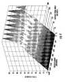
- the graph in FIG. 4illustrates the results of a field diffusion simulation, as an illustration of the field intensity in a 2-D plane.
- the shape-information-bearing quantityis the difference between the peaks and the valleys of the spatial sine wave.
- the graphillustrates how the field generated by a spatially-varying electric field intensity source (at the right side of the graph) attenuates as the distance from the source increases. This simulation illustrates some of the problems to be addressed to more accurately measure the shape of a fingerprint pattern that is remote from the array of finger sensing pixels.
- the attenuation of shape information in the field signalsmay not be uniform for information at different spatial frequencies.
- higher spatial frequenciesare typically attenuated more than lower spatial frequencies, in accordance with the well known field diffusion equations.
- Curves 93, 94, 95, 96illustrate distance versus modulation ratio for 16, 8, 4, and 2 pixels respectively.
- the graph of FIG. 5illustrates the results of simulations indicating how the attenuation is dependent on the spatial frequency content of the shape being measured.
- the graph of FIG. 5uses the modulation ratio as a normalized indication of relative signal strength on the y axis.
- the shape signal(the differences between the peaks and the valleys) attenuates as you move to the left on the graph much faster than the average value of the field.
- the signals at a remote array of finger sensing pixelsmay have very small pixel to pixel differences in the presence of a much larger average signal.
- the small peak to valley differences from the large overall pixel signalsmay be extracted.
- the small difference signalmay be extracted from the larger overall signal at several points within the finger sensing device.
- Each possible location of the extraction functionmay have various advantages and disadvantages. The best choice may depend on the specific details of the system and may vary from finger sensing device. Of particular interest is the constraint that the parts of the overall system that carry information that is represented as small differences between large signals must have a large dynamic range.
- the dynamic range of the remainder of the finger sensing devicemay be reduced at the expense of some increase in complexity at the extraction/nullification point.
- Suppressing the large common signal (discussed above) at the sensor itself, or in the amplification stagemay be useful in reducing the dynamic range of the downstream signal processing and image processing.
- the systemapplies an inverted (and possibly phase shifted for AC sensing) version of the excitation signal (or of the average of the received signal across the array) equally to the array of finger sensing pixels.
- the amplitude of the inverted signalmay optionally be adjusted during imaging to achieve the optimum null.
- the resulting signal fed to the subsequent amplification stagesmay have the majority of the large common mode signal removed, so that the small pixel-to-pixel variations can be amplified without requiring excessive dynamic range from the amplifiers.
- the inverted signalcan be injected directly at the electric field sensing pixel antenna, by placing a small electrode carrying the inverted signal beneath the antenna plates, as will be appreciated by those skilled in the art.
- a high-gain, low-noise sense amplifiermay be used with little considers of saturation.
- the inverted signal insertion mechanism for suppressing large average signals at the array of finger sensing pixelsis advantageous even when the mechanisms discussed below are employed because it may limit the common mode voltages seen at the sense amp inputs.
- the average received signal from a group of finger sensing pixelsmay be used to establish a signal, which is then used as the suppression signal source.
- This mechanismallows the array of sensing pixels to adapt to different overall signal levels, by varying the suppression signal, depending on the situation.
- One way of generating an average signalis to interconnect a group of finger sensing pixels that may not currently be scanned, and measuring the average signal developed on this group of interconnected pixels.
- physical arrays of finger sensing pixelstypically include a small number of pixels that are malfunctioning. The finger sensing device should continue to operate with the least amount of disruption possible in spite of the malfunctioning pixels.
- One method of computing a central tendency signal, that is less sensitive to failure of a small number of pixels than the average signal,is to generate a median signal.
- a filter circuit 60that acts as a weighted median filter which can generate a signal useful for suppressing large common signals in the analog portions of the architecture is illustrated.
- the filter circuit 60may be used in the finger sensing device 20 alone or with additional filters or filtering techniques, for example, differential measurement circuitry 40 that is described in further detail below.
- the filter circuit 60includes differential amplifiers 61a-61k and corresponding resistors 62a-62k that are to be coupled to each finger sensing pixel. Pixel weighting factors may be determined by the relative values of the current summing resistors 62 .
- Vmis the median voltage
- Vpis the pixel feed voltage.
- the amount of attenuation seen in signals representing remote shapes at a particular distancecan vary as a function of the spatial frequency content of that shape information. Therefore, accurate measurement of the remote shapes may require spatial frequency sensitive compensation, or essentially spatial filtering.
- Spatial frequency compensationcan be performed at several different places within the finger sensing device. Spatial filtering may be applied directly at the array of finger sensing pixels, in the analog amplification stage, or digitally after the data conversion in the image generating and processing stage. The same kind of trade-offs take place here as discussed previously regarding the large dynamic ranges for the stages upstream of the spatial frequency compensation, and the costs of incorporating that compensation early in the signal flow versus the reduction in required dynamic range.
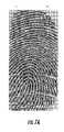
- FIG. 7a-7cillustrate the effects of undesired strong low spatial frequency information in the measurements of fingerprints at a distance from the sensor array.
- FIG. 7aillustrates a fingerprint of a user's finger measured from adjacent the array of finger sensing pixels.
- FIG. 7billustrates the same user's finger measured by an array of finger sensing pixels that are relatively distant from the user's finger. Dominant energy at spatial frequencies lower than the fingerprint frequencies are illustrated.
- FIG. 7cillustrates the same fingerprint after digital spatial filtering. Illustratively, the digital spatial filtering was unable to extract the full ridge pattern fromt eh 4-bit gray scale image.
- Spatial filtering of digital imagesis well understood by those skilled in the art, and can be applied at the image processing stage in the finger sensing device. Spatial frequency compensation may be applied at the finger sensing pixel and amplifier levels by applying the signals from multiple sensors in the array to analog summing and differencing blocks configured to implement the convolution kernel functions for the filtering.
- Passive impedance planessuch as that described in U.S. Patent No. 6,067,368 to Setlak et al. , the entire contents of which are herein incorporated by reference, may be configured to act as spatial high-pass filters, or as unsharp masking filters, providing a form of spatial frequency compensation.
- spatial filtersmay be applied, as will be appreciated by those skilled in the art.
- differential pixel measurement via the differential pixel measurement circuitry 40discussed in further detail below may be applied to reduce the low spatial frequency signals from dominating the system front end dynamic range, and allow the construction of a spatial frequency compensated shape signal in the image processing stage.
- common noise sources in with respect to the sensing stage of a finger sensing devicemay include external interference, excitation noise, intrinsic sensor noise, fixed pattern noise from the array of finger sensing pixels, and ground potential noise.
- Potential noise management techniques to address noise sources in the sensing stagemay include balanced differential measurement (discussed in further detail below), and correlated double sampling.
- common noise sourcesmay include sampling and switching noise, row and column noise, which may include temporal and fixed pattern noise, power rail noise, and component intrinsic noise, which may include temporal and fixed pattern noise.
- Potential noise management techniques to address noise sources in the amplification and signal processing stagemay include differential amplification and signal processing, signal integration, temporal and spatial bandwidth limiting, calibration and compensation, and power rail isolation.
- noise sourcesmay include quantization noise, reference noise, and switching noise.
- Approaches to address noise sources at the conversion stageinclude hi-resolution data conversion and multi-sample averaging.
- noise management approachesmay include spatial filtering and optimal equalization, frame averaging, heuristic estimation, and feature reconstruction.
- noise sources at each of the various stages of the finger sensing deviceand other and/or additional approaches may be used to address these noise sources, as will be appreciated by those skilled in the art.
- the differential pixel measurement circuitry 40advantageously provides a remote shape measuring that applies some elements of the theory behind the delta/sigma method of processing time-series signals to the design of a system for measuring remote shapes, such as fingerprint images.
- the resulting finger sending device 20exhibits the properties to more accurately measure remote shapes as discussed above with reduced impact on cost and complexity compared to standard short distance shape imaging systems.
- a finger sensing device 20that includes the differential pixel measurement circuitry 40 may provide true balanced differential noise cancellation, intrinsic spatial frequency compensation, intrinsic cancellation of large common mode signals, and highly effective use of finger sensing device bandwidth and dynamic range, for example.
- the differential pixel measurement circuitry 40measures the differences between adjacent pixels at the same moment in time.
- Adjacent pixels 31may be pixels that are spaced by any of 0 to 6 pixels intervening for a typical 500 pixel-per-inch sensor and to image typical ridges and valleys, for example.
- the differential measurement circuitry 40may measure the difference between every other pixel, every third pixel, etc.
- the inter-pixel deltas measuredare spatial rather than the temporal deltas typically measured in time-domain delta/sigma processing.
- the measured inter-pixel deltasare processed through the differential pixel measurement circuitry 40 , and the original shape image is reconstructed downstream by integrating the inter-pixel deltas via image processing circuitry 51 .
- Time domain delta/sigma processingtypically includes the use of a 1-bit analog-to-digital convertor and a variable temporal sample rate.
- the differential pixel measurement circuitry 40'includes a differential amplifier 41' coupled between adjacent finger sensing pixels 31 '.
- the measurement of the difference between finger sensing pixels 31 in an array of finger sensing pixels 30can be designed to be a fully balanced differential measurement, with the common mode signal and noise rejection properties typically associated with that style measurement.
- the differential pixel measurementthen provides cancellation of temporal noise and external interference at the pixel sensors, as well as suppressing the large common mode signals inherent in diffusive field measurements.
- the resulting difference signalscan be amplified to useful levels for subsequent processing.
- the intrinsic spatial low-pass filtering property of the field diffusion processmay limit the size of the difference signal that the user's finger 21 may induce between any two adjacent finger sensing pixels 31 in the array of finger sensing pixels 30 . Any measured signal differences larger than a limit may be clipped, without loss of useful data, because these large differences typically cannot represent the real shape of the user's finger 21 , and hence may be spurious.
- the finger sensing device 20includes a 2-dimensional array of finger sensing pixels 30. More particularly, the array of finger sensing pixels 30 includes rows and columns of finger sensing pixels 31 . Thus, it may be beneficial to measure the interpixel differences both in the horizontal direction and the vertical direction, to get a complete set of information about the user finger 21.
- the differential pixel measurement circuitry 40includes a differential amplifier 41 between adjacent finger sensing pixels 30 in each row, and a differential amplifier between adjacent finger sensing pixels in each column. This adds redundancy to the finger sensing device 20 that may be used to reduce noise.
- each finger sensing pixel 31 in the final integrated imagemay be computed by integrating along one of several different "paths" through the array of finger sensing pixels 30 using image generating circuitry 51 , for example. Combining the results of several paths may produce a more robust result, as will be appreciated by those skilled in the art. The use of the multiple paths will be described in further detail below. It should be noted that for two-dimensional difference measurements, there are approximately twice as many measurements performed as there would be if direct measurements of the pixel voltages were made, or if one dimensional measurements were made. The extra measurements may be used to suppress noise and improve accuracy, for example.
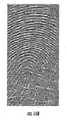
- FIGS. 10a-10cimages of a user's finger are illustrated.
- FIG. 10aillustrates an image of a user's finger made from a standard finger sensing device
- FIGS. 10b and 10cillustrate images of a user's finger that represent the interpixel differences in the vertical and horizontal directions measured on the same user's finger, respectively.
- grayrepresents areas where the adjacent pixels have little or no difference
- whiterepresents a positive difference
- blackrepresents a negative difference.
- each differential measurementis represented as being performed by a separate differential amplifier. While this approach may be used, it may be desirable to implement measurement of the array of finger sensing pixels by switching the signals from different pixels onto a smaller bank of differential amplifiers. To build an economical and reliable finger sensing device using differential pixel measurement circuitry, it may be desirable to add as little circuitry as possible under each of finger sensing pixels 31 .
- each finger sensing pixel 31"includes one side of a balanced differential transistor pair defining a differential amplifier stage 42 ".
- Switching circuitry 43"interconnects these transistors to operate as differential pairs in different configurations at different times, to make different inter-pixel measurements.
- the differential pixel measurement circuitry 40"is balanced.
- the respective differential amplifier stage 42"is coupled to each finger sense electrode 32" of each finger sensing pixel 31".
- Each differential amplifier stage 42"is illustratively in the form of an analog transistor, for example.
- the switching circuitry 43"selectively couples respective pairs of differential amplifier stages 42" in a differential configuration for the adjacent pairs of the finger sensing pixels 31".
- adjacent pixels 31"may be pixels that are spaced by any of 0 to 6 pixels intervening for a typical 500 pixel-per-inch sensor and to image typical ridges and valley, for example.
- the switching circuitry 43"includes two pixel busses 44a", 44b" , and a bank of bus switches 45" for each row that allows the busses to be switched into the various configurations needed to interconnect the finger sensing pixels 31" in the row into the differential transistor stages 41".
- the switching circuitry 43"also illustratively includes respective analog switches in the form of an analog switching transistor 46" coupled to each finger sensing pixel 31" .
- the alternating connection of the finger sensing pixels 31" to the two sets of busses 44a", 44b”allows two adjacent pixels 31" in the same row to be connected together as a balanced differential pair, as will be appreciated by those skilled in the art.
- An output stage 48which is illustratively in the form of a differential amplifier, is coupled to the switching circuitry 43" .
- the measured signali.e. measured interpixel difference measurement, is output from the output stage 48"
- finger sensing pixels 31"While only two finger sensing pixels 31" are illustrated, it should be understood that additional finger sensing pixels in a row may be added, and several rows of finger sensing pixels may also be included. Each row of finger sensing pixels would have their associated busses, switch banks and amplifiers, as will be appreciated by those skilled in the art.
- Image generating circuitry 51"is coupled to the differential measurement circuitry 40 " , and more particularly, may be coupled to the output stage 48 ".
- the image generating circuitrymay be configured to generate a composite finger image based upon the interpixel measurements for adjacent pairs of the finger sensing pixels 31" along both the rows and columns of the array of finger sensing pixels 30 ".
- Respective output stages 48 " representing each row of pixelsmay be integrated, for example, to generate the composite finger image.
- Other composite finger image generation techniquesmay be used, as will be appreciated by those skilled in the art.
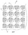
- FIGS. 13a-13fa scanning sequence for use with a finger sensing device to sequentially read all of the differential pixel voltages across the array of finger sensing pixels 30" according to an embodiment of the present invention is illustrated.
- the array of finger sensing pixelsis illustratively an 8 x 8 array of finger sensing pixels.
- This scan sequenceassumes that there are 8 row amplifier/switch bank structures of the type discussed above, one associated with each row of pixels. It further assumes that these amplifiers can operate in parallel, so that up to eight differential pixel measurements can be performed simultaneously during each scan step.
- FIGS. 13a-13frepresents a scan step, and illustrates which finger sensing pixels in the array are differentially connected and being measured.
- the black lines 71" interconnecting the darker and lighter dots 72", 73"indicate pixels that are connected together into differential pairs, and the darker and lighter dots are each coupled to a respective bus.
- other sequencescan be used that can include varying degrees of measurement redundancy and which may as a result have enhanced noise reduction benefits.
- bussing and switching arrangements described aboveare examples of a wide range of different bussing and switching configurations that may be used to interconnect the finger sensing pixels into the differential amplifier configurations.
- a double bus beneath the finger sensing pixels that interconnects the pixels' analog switches to the column current sinkmay be reduced to a single bus with a reduced complexity switching bank, at the cost of less flexibility in the scanning sequences that can be supported, as will be appreciated by those skilled in the art.
- the differential pixel measurement datacan be used in its raw form directly (or with only minor modifications/enhancements) without actually reconstructing the shape of the user's finger.
- the edges of the fingerprint ridgesare clearly present in the image representation of the pixel difference data. Often this information is quite usable in that form.
- the differential pixel data from several frames of the data streammay be used to estimate the movement of the user's finger object with respect to the array of finger sensing pixels.
- the correlation estimation methods typically used for this taskcan make effective use of the edge information contained in the differential pixel data.
- some types of finger sensing devicerely on extracting and matching the regional orientation of the ridge pattern.
- the ridge orientation vector field of a fingerprintcan, in this example case, be readily extracted directly from the from the differential pixel measurements.
- the confidence level of each of the ridge direction vectorsis indicated by the intensity of the vector, with darker vectors being a highest confidence level and lighter vectors being a lowest confidence.
- the pattern of interestmay be included in information within a limited spatial frequency band. Spatial frequencies outside that band, both above and below, may constitute noise to the pattern recognition system and are typically removed by filtering or other means. For example in fingerprint pattern matching, information having spatial frequencies significantly lower or significantly higher than the friction ridge frequency hinders recognition. In these applications the shape image collection system can be simplified by removing the undesired information early in the process and not carrying that information through the system.
- low spatial frequenciesmay be removed from the output image by restricting the region of pixel differences that are integrated to contribute to the value each output pixel to a small kernel. Spatial wavelengths that are significantly larger than the kernel size may have little effect on the output of the kernel integration.
- One way to look at kernel integrationis to consider averaging the values derived by following several paths through various pixel difference measurements to the pixel whose output value is being value calculated.
- the image generating circuitry 51'"includes kernel processing circuitry 52'" which is configured to compute the value of each finger sensing pixel 31"' from the difference measurements made in the vicinity to a given finger sensing pixel.
- Pixel Value⁇ W 1 ⁇ ⁇ oneStepPath i ⁇ 1 + W 2 ⁇ ⁇ oneStepPath i ⁇ 2 + ...
- the array of weights W nconstitutes a filtering kernel that can impart spatial frequency response tailoring to the finger sensing device.
- the array of finger sensing pixels 31"'can be more or less sensitive to different spatial frequencies.
- each finger sensing pixel's valueis computed from multiple partially-redundant measurements made using different finger sensing pixel transistors at different times, both fixed pattern noise and temporal noise can be reduced.
- the two dimensional properties of the array of finger sensing pixels 30"'enhance this effect by providing more measurement redundancy.
- the finger sensing device 20"'behaves like as a spatial highpass filter in the sense that spatial DC signals, e.g., uniform offsets in the array signals) typically do not affect the measurements. If the array of finger sensing pixels 30'" is moving across a larger image, for example, and capturing frames as it moves, spatial frequencies with wavelengths smaller than the size of the array of finger sensing pixels may be not present in the reconstructed image unless special consideration is taken when reconstructing the image across frame boundaries, as will be appreciated by those skilled in the art.
- the shape reconstruction processmay also be structured to compensate for the spatial frequency specific attenuation that occurs in remote measurements using diffusive fields.
- One way to accomplish thisis to design the integration method used for reconstruction to re-emphasize the spatial frequencies that have been more strongly attenuated in the remote field propagation process.
- the approach illustrated in FIG. 16includes one representation of spatial frequency compensation in the reconstruction process.
- an alternate representation of the shape reconstruction processmay be implemented.
- the adaptation of classic spatial filtering convolution kernelsprovides a spatial frequency tailored reconstruction of the user's finger information. More particularly, a weighting matrix that generates the spatial frequency compensation can be based upon the distance from the pixel being calculated.
- the sign of the contribution from each delta pixel measurement contributing to the pixel being calculatedgenerally depends on the signs of the polarity of the differential measurements. For the horizontal deltas, measurements to the left of the pixel being calculated are accumulated with the opposite sign from those on the right. For the vertical deltas, measurements above the pixel being calculated will be accumulated with the opposite sign from those below.
- the kernel for the image construction operationcan be the horizontal and vertical spatial frequency weighting matrix, with the signs modified to reflect the left/right and up/down criterion.
- Pixel Value⁇ Kh i , j ⁇ ⁇ hi , j + ⁇ Kv i , j ⁇ ⁇ v i , j
- the orientation of strongly linear patternssuch as, for example, fingerprints
- That orientation informationalong with the pattern's spatial frequency information which may also be derived from the difference measurements, can be used to orient the kernel filtering circuitry 52'" as an asymmetric-kernel shape reconstruction filter.
- Such a filtercan provide significant noise cancellation and image quality improvements for patterns with strongly oriented textures.
- the finger sensing device 20advantageously reads fingerprints from a user's finger positioned at a larger distance away from the array of finger sensing pixels 30 . This allows a number of different mechanical packaging and host device integration approaches that may mitigate the disadvantages of specialized packaging and problems with mechanical integration.
- these approachesmay include overmolded IC packages, which are a relatively low cost, high yield packaging of fingerprint sensing ICs that use standard molded packages that do not have an opening over the array of finger sensing pixels.
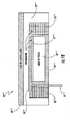
- the finger sensing device 20""includes an overmolding 53"" is over the array of finger sensing pixels 30"", the finger drive electrode 32"", and a bond wire 54"".
- a color coat layer 55""is over the overmolding 53""
- a surface clear coat layer 56"”is over the color coat layer.
- the thickness of the overmolding 53"" and clear and color coat layers 55"", 56””may be in a range of 100-900 microns, for example. This may reduce the need for special thin coatings that are currently used over the array of finger sensing pixels, replacing it with the standard mold compound. It may also reduce special manufacturing and handling equipment and practices associated with these sensors.
- a flip chip underfill 57""'is carried by array of finger sensing pixels 30""'
- a backfill 58""'surrounds the sides and underneath of the array of finger sensing pixels 30""' .
- a bond wire 54""'couples through the backfill 58""' .
- a interconnection substrate 59""'for example, a Kapton substrate, is over the flip chip underfill 57""' and partially over the finger drive electrode 32""' .
- Overmoldingis carried above the interconnection substrate 59""' along the length of the finger sensing device 20""'.
- a film top surface layer 64""'is carried by the overmolding 53""' .
- a finger sensing device 20""'that can work with standard thicknesses of plastic material molded over them may be molded as an integral part of a molded key cap, something that is relatively difficult with current sensors.
- the finger sensing device 20 described hereinmay be embedded into standard laminated identification (ID) cards.
- IDlaminated identification
- a finger sensing device that can image the user's finger through standard laminations used in smartcard and RF-ID card fabricationmay now be economically built into those cards, using standard low cost card assembly processes.
- Total imaging distancesfor fingerprint imaging from underneath device external structures all distances shown in microns Total imaging thickness Structure thickness wire bond BGA COF thru Si via BGA Structure name min max min max min max min max Cellphone case thicknesses 400 800 625 1025 475 875 440 840 Image through thinned area in the case of a cellphone - no surface hole 125 250 350 475 200 325 165 290 Image through a cellphone keyboard membrane 125 175 350 400 200 250 165 215 Image through an LCD display cover plate 350 700 575 925 425 775 390 740 Image through a touchpad membrane 125 300 350 525 200 375 165 340 Image through a molded key cap 75 150 300 375 150 225 115 190 Image through smart card structural film (PET) 75 125 300 350 150 200 115 165
- a method aspectis directed to a method of sensing a finger.
- the methodmay include receiving a user's finger adjacent an array of finger sensing pixels, each finger sensing pixel comprising a finger sensing electrode.
- the methodalso includes coupling a drive signal through the user's finger to the array of finger sensing pixels via a finger drive electrode.
- the methodalso includes generating a plurality of interpixel difference measurements for adjacent pairs of the finger sensing pixels using differential pixel measurement circuitry coupled to the array of finger sensing pixels.
- circuitry described hereinmay include all hardware, or a combination of hardware and software or computer-executable instructions that are executed on a processor.
- more than one processormay be used, and the processing may be shared across the processors, for example, with a host processor.
- Other processing and hardware/software configurationsmay be used, as will be appreciated by those skilled in the art.
Landscapes
- Engineering & Computer Science (AREA)
- Physics & Mathematics (AREA)
- General Physics & Mathematics (AREA)
- Multimedia (AREA)
- Theoretical Computer Science (AREA)
- Human Computer Interaction (AREA)
- Computer Vision & Pattern Recognition (AREA)
- Measurement Of The Respiration, Hearing Ability, Form, And Blood Characteristics Of Living Organisms (AREA)
- Image Input (AREA)
- Measurement Of Length, Angles, Or The Like Using Electric Or Magnetic Means (AREA)
Description
- The present invention relates to the field of electronics, and, more particularly, to finger sensing devices and related methods.
- Fingerprint sensing and matching is a reliable and widely used technique for personal identification or verification. In particular, a common approach to fingerprint identification involves scanning a sample fingerprint or an image thereof and storing the image and/or unique characteristics of the fingerprint image. The characteristics of a sample fingerprint may be compared to information for reference fingerprints already in a database to determine proper identification of a person, such as for verification purposes.
- In recent years it has been practical and economical to build high-quality electronic fingerprint sensing devices using radio-frequency (RF) electric fields to develop an electronic representation of the fingerprint pattern. Such devices have been fabricated as standard CMOS integrated circuits on monocrystalline silicon substrates. These processes allow the electronic structures necessary to read the signal from each of the sensor's pixels or sensing electrodes to be fabricated directly beneath the pixels. Locating the signal conditioning electronics or sense amps under pixel was important to adequate performance of the circuitry.
- One such RF fingerprint sensing device is disclosed in
U.S. Pat. No. 5,940,526 to Setlak et al. and assigned to the assignee of the present invention. The patent discloses an integrated circuit fingerprint sensor including an array of RF sensing electrodes to provide an accurate image of the fingerprint friction ridges and valleys. More particularly, the RF sensing permits imaging of live tissue just below the surface of the skin to reduce spoofing, for example. The entire contents of the Setlak et al. patent are incorporated herein by reference. - Another example of a fingerprint sensing device is disclosed in
U.S. Pat. No. 5,325,442 to Knapp . The fingerprint sensing device has a row/column array of sense elements which are coupled to a drive circuit and a sense circuit by sets of row and column conductors, respectively. The sense elements are actively addressable by the drive circuit. Each sense element includes a sense electrode and a switching device, such as a thin film transistor (TFT) switching device, for active addressing of that sense electrode. The sense electrodes are covered by an insulating material and are for receiving a finger. Capacitances resulting from individual finger surface portions in combination with sense electrodes are sensed by the sense circuit by applying a potential to the sense electrodes and measuring charging characteristics. - Historically, electronic integrated circuits generally achieve reduced fabrication costs by using fabrication processes with smaller electronic device geometries. With smaller device geometries the circuit itself becomes smaller, using less silicon, and thus costs less to fabricate. Electronic fingerprint sensors, however, generally cannot be made smaller than the area of the finger skin that needs to be imaged. Smaller component geometries may not reduce the fingerprint sensor die size or cost significantly. One of the only result of smaller component geometries may be unused silicon space under the sensor pixels.
- One approach to reducing the cost of fingerprint sensing is to design systems that can work effectively using images of smaller areas of skin. This approach has been used in a variety of devices. A second approach is to use sliding sensors. With sliding sensors, either the finger or the sensor move during the data acquisition process, which allows a small sensor to generate images of larger pieces of skin. Yet, the sliding sensors may be subject to significant image distortion, and/or they may provide an inconvenient user paradigm.
- Image distortion or noise may also be present when it may be desirable to sense a finger image from fingers positioned at a relatively greater distance away from an array of finger sensing pixels. For example, it may be desirable to extend the range of electric field based finger sensors so that they can image fingers through significantly thicker dielectric materials such as molded plastic structures. An example of prior art is
WO 2007/011607 A1 , which relates to an electronic fingerprint sensor with differential noise cancellation. - Integrated circuit based fingerprint sensors used in personal electronic devices, such as, for example, laptop computers and cellular telephones may be generally effective sensing fingers for user identity authentication. However, these finger sensors generally require the finger to be placed in a very close proximity to the array of finger sensing pixels. The need for close proximity to the user's finger typically makes the mechanical packaging and the integration of these devices into their host products more difficult and more costly.
- Some approaches to address integrated circuit packaging of these devices include a special molded package with an opening in the molding allowing the finger a close approach to the array, and a specialized packaging on thin flex circuit substrates that allows the finger to be placed close to the sensing array, for example. Specialized packaging increases the cost of these sensors.
- The need for the user's finger to be close to the array of finger sensing pixels may limit the thickness of the material that can be placed over that array, which may increasingly restrict the use of both protective and cosmetic coatings over the array area. Mechanically integrating these sensors into their host devices typically requires that the finger sensor project through a hole in the host device's case, so that the array of finger sensing pixels can be located about flush with the external surface of the case.
- However, a negative aspect of these mounting arrangements may include increased difficultly and cost to seal opening for the finger sensor in the host device case against the ingress of moisture, dust, and other contaminants. Additionally, the opening in the case with the finger sensor protruding may be cosmetically unacceptable to the intended appearance of the host device, and mounting the finger sensor in an opening in the case may be difficult and costly in some devices.
- In view of the foregoing background, it is therefore an object of the present invention to provide a finger sensing device that can generate a reduced noise finger image from a finger positioned at a relatively large distance from the array of finger sensing pixels.
- This and other objects, features, and advantages in accordance with the present invention are provided by a finger sensing device as claimed in
claim 1. - Accordingly, the finger sensing device may generate a reduced noise finger image from a finger positioned at a relatively large distance from the array of finger sensing pixels.
- The finger sensing device may further include a cover layer over the finger sensing pixels having a thickness in a range of 100-900 microns, for example. The differential pixel measurement circuitry may include balanced differential pixel measurement circuitry. The balanced differential pixel measurement circuitry may include a respective differential amplifier stage coupled to each finger sense electrode of each finger sensing pixel and switching circuitry to selectively couple respective pairs of differential amplifier stages in a differential configuration for the adjacent pairs of the finger sensing pixels. The balanced differential pixel measurement circuitry may also include an output stage coupled to the switching circuitry, for example.
- The array of finger sensing pixels may include rows and columns of finger sensing pixels. The differential pixel measurement circuitry may include switching circuitry for generating the plurality of interpixel measurements for adjacent pairs of the finger sensing pixels along both rows and columns of the array of finger sensing pixels, for example. The finger sensing device may further include image generating circuitry coupled to the differential measurement circuitry and configured to generate a composite finger image based upon the interpixel measurements for adjacent pairs of the finger sensing pixels along both rows and columns of the array of finger sensing pixels, for example.
- The image generating circuitry may further include kernel filtering circuitry coupled to the differential measurement. The finger sensing device may further include a semiconductor substrate, for example. The array of finger sensing pixels may be on the semiconductor substrate. The finger sensing device may further include a radio frequency drive signal generator coupled to the finger drive electrode.
- A method aspect is directed to a method of a method of sensing a finger that may include receiving a user's finger adjacent an array of finger sensing pixels, each finger sensing pixel comprising a finger sensing electrode. The method may also include coupling a drive signal through the user's finger to the array of finger sensing pixels via a finger drive electrode, for example. The method may further include generating a plurality of interpixel difference measurements for adjacent pairs of the finger sensing pixels using differential pixel measurement circuitry coupled to the array of finger sensing pixels, for example.
FIG. 1 is a schematic block diagram of a finger sensing device in accordance with the present invention.FIG. 2 is a graph of skin electrical properties versus drive signal attenuation.FIG. 3 is a graph of skin electrical properties versus drive signal attenuation for direct and insulated drive finger contact arrangements.FIG. 4 is a graph of electric field intensity in a 2-dimensional plane.FIG. 5 is a graph of modulation ratios versus distance from the array of finger sensing pixels for different sized arrays of finger sensing pixels.FIG. 6 is a schematic diagram of an analog implementation of a weighted median filter for use with the finger sensing device of the present invention.FIGS. 7a-7c are fingerprint images illustrating the effects of low spatial frequency at a distance from the array of finger sensing pixels.FIG. 8 is a schematic diagram of a portion of a finger sensing device having a one-dimensional array of finger sensing pixels in accordance with the present invention.FIG. 9 is a schematic diagram of a potion of finger sensing device having a two-dimensional array of finger sensing pixels in accordance with another embodiment of the present invention.FIGS. 10a-10c are fingerprint images showing horizontal and vertical differences.FIG. 11 is a schematic block diagram of a finger sensing device according to another embodiment of the present invention.FIG. 12 is a schematic circuit diagram of a portion of a finger sensing device ofFIG. 11 .FIGS. 13a-13f are schematic illustrations of a possible scan pattern for an array of finger sensing pixels of a finger sensing device according to the present invention.FIGS. 14a and14b are greatly enlarged fingerprint images including ridge orientation vectors extracted from vertical and horizontal pixel differences, respectively.FIG. 15 is a schematic block diagram of a finger sensing device according to another embodiment.FIG. 16 is a schematic diagram illustrating kernel based reconstruction according to the embodiment inFIG. 15 .FIG. 17 is a schematic diagram of an overmolded package arrangement including the finger sensing device of an embodiment of the present invention.FIG. 18 is a schematic diagram of a standard pushbutton package arrangement including the finger sensing device of an embodiment of the present invention.- The present invention will now be described more fully hereinafter with reference to the accompanying drawings, in which preferred embodiments of the invention are shown. This invention may, however, be embodied in many different forms. These embodiments are provided so that this disclosure will be thorough and complete, and will fully convey the scope of the invention to those skilled in the art. Like numbers refer to like elements throughout, and prime and multiple prime notation is used to indicate similar elements in alternative embodiments.
- Referring initially to
FIG. 1 , afinger sensing device 20 includes an array offinger sensing pixels 30 to receive a user'sfinger 21 adjacent thereto. The array offinger sensing pixels 30 are carried by asemiconductor substrate 22. The array offinger sensing pixels 30 may be any array size, as will be appreciated by those skilled in the art. Eachfinger sensing pixel 31 may be an electric-field sensing pixel. In some embodiments, each finger sensing pixel may be a capacitive sensing pixel, for example, or other type of sensing pixel. Eachfinger sensing pixel 31 includes afinger sensing electrode 32. Afinger drive electrode 33 is configured to couple a drive signal through the user'sfinger 21 to the array offinger sensing pixels 30. Of course, thefinger drive electrode 33 may couple a drive signal through more than one user's finger, and more than one finger drive electrode may be used. A radio frequencydrive signal generator 36 is coupled to thefinger drive electrode 33. - As will be appreciated by those skilled in the art, the
finger sensing device 20 operates by injecting a small electrical signal from thefinger drive electrode 33 into the conductive layer of the skin of the user'sfinger 21. The shape of the electric field generated by that conductive layer of skin is then measured. - The
finger drive electrode 33 may be configured to inject the small electrical signals into the users' finger in one of two ways. Thefinger drive electrode 33 may be configured to operate as a contact electrode finger drive. Alternatively or additionally, thefinger drive electrode 33 may be configured to operate as an insulated electrode finger drive. Thefinger drive electrode 33 may be configured to operate using other techniques, for example, electric and magnetic induction techniques. - When the
finger drive electrode 33 is configured to operate as a contact electrode finger drive, an electrically conductive surface makes direct electrical contact with the surface of the user'sfinger 21. Electrical signals on thefinger drive electrode 33 are coupled into the user'sfinger 21 with varying degrees of attenuation, where the attenuation depends on the size of the finger-to-electrode contact area, and on the electrical properties of the finger skin itself. It should be noted that the electrical properties of finger skin may vary from person to person and from moment to moment over a range of several orders of magnitude. - The
curves FIG. 2 are derived from electrical modeling and show the drive signal attenuation inside a user'sfinger 21 as a function of the contact area and skin electrical properties. The skin electrical properties range from very thick dry skin at the left of the chart to thin moist skin at the right of the graph. The four different curves represent four different finger contact areas, with the upper curve81 representing the largest area and thelower curve 84 representing the smallest area. - When the
finger drive electrode 33 is configured as an insulated electrode finger drive, an electrically conductive electrode is separated from the surface of the user'sfinger 21 by a thickness of insulating material. Electrical signals on an insulated electrode couple capacitively to nearby skin surfaces. For insulated electrodes, the signal attenuation due to coupling depends on the combination of several parameters including the area of the region of skin close to the electrode, the thickness of the insulating material between the electrode and the finger, the electrical properties of that insulating material, and the electrical properties of the finger skin itself. - The curves illustrated in the graph of
FIG. 3 , derived from electrical modeling, compare finger drive signal attenuation for direct contactfinger drive arrangements finger drive arrangements - It may be important to note that insulated finger drive systems tend to reduce the variation in drive signal attenuation between the dry, thick skinned fingers and the moist, thin skinned fingers. In the example above, the insulated drive handles the finger skin variation with half the dynamic range for the direct drive system. In general, if a fixed voltage boost is applied to the insulated finger drive electrode system to overcome the differences in average attenuation, the resulting system may demand significantly less dynamic range to handle finger skin variation than a direct drive system as shown by the
curves - The array of
finger sensing pixels 30 includes rows and columns of finger sensing pixels. Two dimensional arrays offinger sensing pixels 31 are often used to measure the shapes of remote objects, by measuring the intensity of an energy field that has been affected by the remote target object, for example, the user'sfinger 21. Typically the energy measured by eachpixel 31 of thearray 30 is used to set a pixel value in an image of the remote object. An example of such remote sensing is the measurement of fingerprint patterns of fingers that are not in contact with the sensor array, but are separated from that array by protective material of various thicknesses. In a typical system of this type, the shape information (a spatial signal impressed on the underlying field) becomes attenuated as the target object is moved further from the array of finger sensing pixels. - To more effectively measure the attenuated spatial signals that represent the user's finger shape information when the user's finger is a significant distance from the sensor array, the finger sensing device20' includes differential
pixel measurement circuitry 40. coupled to the array offinger sensing pixels 30 and configured to generate a plurality of interpixel difference measurements for adjacent pairs of thefinger sensing pixels 31. - As will be described in further detail below, the differential
pixel measurement circuitry 40 advantageously address the problems of measuring shape information from very small signal differences betweenfinger sensing pixels 31 having large overall signals on them, and measuring attenuated high-spatial-frequency signals in the presence of strong lower-spatial-frequency signals. Thedifferential measurement circuitry 40 also advantageously measures the weak spatial signals while reducing noise. As will be appreciated by those skilled in the art the differentialpixel measurement circuitry 40 may use spatial analog to delta/sigma time series measurements to accomplish the above-noted objectives. - The attenuation of the shape information with distance is more evident in arrays of electric field finger sensing pixels that are used to measure fingerprints. RF electric fields such as used in these finger sensing devices may be modeled as simple diffusive fields, and the spatial information attenuation analyzed in such a model.
- The graph in
FIG. 4 illustrates the results of a field diffusion simulation, as an illustration of the field intensity in a 2-D plane. In the graph, the shape-information-bearing quantity is the difference between the peaks and the valleys of the spatial sine wave. The graph illustrates how the field generated by a spatially-varying electric field intensity source (at the right side of the graph) attenuates as the distance from the source increases. This simulation illustrates some of the problems to be addressed to more accurately measure the shape of a fingerprint pattern that is remote from the array of finger sensing pixels. - In addition, the attenuation of shape information in the field signals may not be uniform for information at different spatial frequencies. In finger sensing device including electric field based finger sensing pixels that do not use focusing mechanisms, higher spatial frequencies are typically attenuated more than lower spatial frequencies, in accordance with the well known field diffusion equations.
Curves FIG. 5 illustrates the results of simulations indicating how the attenuation is dependent on the spatial frequency content of the shape being measured. The graph ofFIG. 5 uses the modulation ratio as a normalized indication of relative signal strength on the y axis. Features of the largest size93 (16 pixels in this simulation) have the lowest spatial frequency, and experience the least attenuation with increasing distance. - Based upon the graph in
FIG. 4 , the shape signal (the differences between the peaks and the valleys) attenuates as you move to the left on the graph much faster than the average value of the field. As a result, the signals at a remote array of finger sensing pixels may have very small pixel to pixel differences in the presence of a much larger average signal. Ultimately, to reproduce the fingerprint pattern shape the small peak to valley differences from the large overall pixel signals may be extracted. - The small difference signal may be extracted from the larger overall signal at several points within the finger sensing device. Each possible location of the extraction function may have various advantages and disadvantages. The best choice may depend on the specific details of the system and may vary from finger sensing device. Of particular interest is the constraint that the parts of the overall system that carry information that is represented as small differences between large signals must have a large dynamic range. By placing the process that extracts the small pixel-to-pixel signal (or conversely nullifies the large common signal) early in the processing chain, the dynamic range of the remainder of the finger sensing device may be reduced at the expense of some increase in complexity at the extraction/nullification point.
- Suppressing the large common signal (discussed above) at the sensor itself, or in the amplification stage may be useful in reducing the dynamic range of the downstream signal processing and image processing. In one method, the system applies an inverted (and possibly phase shifted for AC sensing) version of the excitation signal (or of the average of the received signal across the array) equally to the array of finger sensing pixels. The amplitude of the inverted signal may optionally be adjusted during imaging to achieve the optimum null. The resulting signal fed to the subsequent amplification stages may have the majority of the large common mode signal removed, so that the small pixel-to-pixel variations can be amplified without requiring excessive dynamic range from the amplifiers.
- In electric-field based finger sensing devices, the inverted signal can be injected directly at the electric field sensing pixel antenna, by placing a small electrode carrying the inverted signal beneath the antenna plates, as will be appreciated by those skilled in the art. By suppressing the relatively strong common signal at the antenna, a high-gain, low-noise sense amplifier may be used with little considers of saturation.
- The inverted signal insertion mechanism for suppressing large average signals at the array of finger sensing pixels is advantageous even when the mechanisms discussed below are employed because it may limit the common mode voltages seen at the sense amp inputs.
- In one implementation, the average received signal from a group of finger sensing pixels may be used to establish a signal, which is then used as the suppression signal source. This mechanism allows the array of sensing pixels to adapt to different overall signal levels, by varying the suppression signal, depending on the situation. One way of generating an average signal is to interconnect a group of finger sensing pixels that may not currently be scanned, and measuring the average signal developed on this group of interconnected pixels. In real-world use, physical arrays of finger sensing pixels typically include a small number of pixels that are malfunctioning. The finger sensing device should continue to operate with the least amount of disruption possible in spite of the malfunctioning pixels. One method of computing a central tendency signal, that is less sensitive to failure of a small number of pixels than the average signal, is to generate a median signal.
- Referring now additionally to the schematic diagram in
FIG. 6 , afilter circuit 60 that acts as a weighted median filter which can generate a signal useful for suppressing large common signals in the analog portions of the architecture is illustrated. Thefilter circuit 60 may be used in thefinger sensing device 20 alone or with additional filters or filtering techniques, for example,differential measurement circuitry 40 that is described in further detail below. Thefilter circuit 60 includes differential amplifiers61a-61k and corresponding resistors62a-62k that are to be coupled to each finger sensing pixel. Pixel weighting factors may be determined by the relative values of the current summing resistors62. Vrx, the voltage through a summing resistor62 is determined by Vrx = V+ if (Vpx > Vm) and Vrx = V- if (Vpx <= Vm). Vm is the median voltage and Vp is the pixel feed voltage. The weighted median filter may be expressed as: Σ (Vrn - Vm)*Rn = 0 for n =1 to k. - As can be seen from the graph in
FIG. 5 , the amount of attenuation seen in signals representing remote shapes at a particular distance can vary as a function of the spatial frequency content of that shape information. Therefore, accurate measurement of the remote shapes may require spatial frequency sensitive compensation, or essentially spatial filtering. - Spatial frequency compensation can be performed at several different places within the finger sensing device. Spatial filtering may be applied directly at the array of finger sensing pixels, in the analog amplification stage, or digitally after the data conversion in the image generating and processing stage. The same kind of trade-offs take place here as discussed previously regarding the large dynamic ranges for the stages upstream of the spatial frequency compensation, and the costs of incorporating that compensation early in the signal flow versus the reduction in required dynamic range.
- Referring additionally to
FIG. 7a-7c the effects of undesired strong low spatial frequency information in the measurements of fingerprints at a distance from the sensor array are illustrated.FIG. 7a illustrates a fingerprint of a user's finger measured from adjacent the array of finger sensing pixels.FIG. 7b illustrates the same user's finger measured by an array of finger sensing pixels that are relatively distant from the user's finger. Dominant energy at spatial frequencies lower than the fingerprint frequencies are illustrated.FIG. 7c illustrates the same fingerprint after digital spatial filtering. Illustratively, the digital spatial filtering was unable to extract the full ridge pattern fromt eh 4-bit gray scale image. - Spatial filtering of digital images is well understood by those skilled in the art, and can be applied at the image processing stage in the finger sensing device. Spatial frequency compensation may be applied at the finger sensing pixel and amplifier levels by applying the signals from multiple sensors in the array to analog summing and differencing blocks configured to implement the convolution kernel functions for the filtering.
- Passive impedance planes, such as that described in
U.S. Patent No. 6,067,368 to Setlak et al. , the entire contents of which are herein incorporated by reference, may be configured to act as spatial high-pass filters, or as unsharp masking filters, providing a form of spatial frequency compensation. A variety of analog and digital implementations of spatial filters may be applied, as will be appreciated by those skilled in the art. - In addition, methods such as differential pixel measurement via the differential
pixel measurement circuitry 40, discussed in further detail below may be applied to reduce the low spatial frequency signals from dominating the system front end dynamic range, and allow the construction of a spatial frequency compensated shape signal in the image processing stage. - As finger sensing devices measure smaller and smaller signals, the ability to reject or nullify noise becomes more and more important. For example, common noise sources in with respect to the sensing stage of a finger sensing device may include external interference, excitation noise, intrinsic sensor noise, fixed pattern noise from the array of finger sensing pixels, and ground potential noise. Potential noise management techniques to address noise sources in the sensing stage may include balanced differential measurement (discussed in further detail below), and correlated double sampling.
- With respect to the amplification and signal processing stage of a finger sensing device, common noise sources may include sampling and switching noise, row and column noise, which may include temporal and fixed pattern noise, power rail noise, and component intrinsic noise, which may include temporal and fixed pattern noise. Potential noise management techniques to address noise sources in the amplification and signal processing stage may include differential amplification and signal processing, signal integration, temporal and spatial bandwidth limiting, calibration and compensation, and power rail isolation.
- With respect to the data conversion stage of the finger sensing device, common noise sources may include quantization noise, reference noise, and switching noise. Approaches to address noise sources at the conversion stage include hi-resolution data conversion and multi-sample averaging. In the image processing stage of the finger processing device, noise management approaches may include spatial filtering and optimal equalization, frame averaging, heuristic estimation, and feature reconstruction. Of course, there may other noise sources at each of the various stages of the finger sensing device, and other and/or additional approaches may be used to address these noise sources, as will be appreciated by those skilled in the art.
- The differential
pixel measurement circuitry 40 advantageously provides a remote shape measuring that applies some elements of the theory behind the delta/sigma method of processing time-series signals to the design of a system for measuring remote shapes, such as fingerprint images. The resultingfinger sending device 20 exhibits the properties to more accurately measure remote shapes as discussed above with reduced impact on cost and complexity compared to standard short distance shape imaging systems. - As will be appreciated by those skilled in the art, a
finger sensing device 20 that includes the differentialpixel measurement circuitry 40 may provide true balanced differential noise cancellation, intrinsic spatial frequency compensation, intrinsic cancellation of large common mode signals, and highly effective use of finger sensing device bandwidth and dynamic range, for example. Rather than measuring the signals on eachfinger sensing pixel 31 in the array offinger sensing pixels 30, the differentialpixel measurement circuitry 40 measures the differences between adjacent pixels at the same moment in time.Adjacent pixels 31 may be pixels that are spaced by any of 0 to 6 pixels intervening for a typical 500 pixel-per-inch sensor and to image typical ridges and valleys, for example. In some embodiments, thedifferential measurement circuitry 40 may measure the difference between every other pixel, every third pixel, etc. Hence, the inter-pixel deltas measured are spatial rather than the temporal deltas typically measured in time-domain delta/sigma processing. The measured inter-pixel deltas are processed through the differentialpixel measurement circuitry 40, and the original shape image is reconstructed downstream by integrating the inter-pixel deltas viaimage processing circuitry 51. - Referring now additionally to
FIG. 8 , an embodiment of a portion of a finger sensing device20' including a 1-dimensional array of finger sensing pixels30' and differential pixel measurement circuitry40' that implements the spatial delta/sigma measurement is illustrated. Time domain delta/sigma processing typically includes the use of a 1-bit analog-to-digital convertor and a variable temporal sample rate. The differential pixel measurement circuitry40' includes a differential amplifier41' coupled between adjacent finger sensing pixels31'. - The measurement of the difference between
finger sensing pixels 31 in an array offinger sensing pixels 30 can be designed to be a fully balanced differential measurement, with the common mode signal and noise rejection properties typically associated with that style measurement. The differential pixel measurement then provides cancellation of temporal noise and external interference at the pixel sensors, as well as suppressing the large common mode signals inherent in diffusive field measurements. The resulting difference signals can be amplified to useful levels for subsequent processing. - It should be noted that the intrinsic spatial low-pass filtering property of the field diffusion process may limit the size of the difference signal that the user's
finger 21 may induce between any two adjacentfinger sensing pixels 31 in the array offinger sensing pixels 30. Any measured signal differences larger than a limit may be clipped, without loss of useful data, because these large differences typically cannot represent the real shape of the user'sfinger 21, and hence may be spurious. - Referring now additionally to
FIG. 9 , thefinger sensing device 20 includes a 2-dimensional array offinger sensing pixels 30. More particularly, the array offinger sensing pixels 30 includes rows and columns offinger sensing pixels 31. Thus, it may be beneficial to measure the interpixel differences both in the horizontal direction and the vertical direction, to get a complete set of information about theuser finger 21. To accomplish this, the differentialpixel measurement circuitry 40 includes a differential amplifier41 between adjacentfinger sensing pixels 30 in each row, and a differential amplifier between adjacent finger sensing pixels in each column. This adds redundancy to thefinger sensing device 20 that may be used to reduce noise. The value of eachfinger sensing pixel 31 in the final integrated image may be computed by integrating along one of several different "paths" through the array offinger sensing pixels 30 usingimage generating circuitry 51, for example. Combining the results of several paths may produce a more robust result, as will be appreciated by those skilled in the art. The use of the multiple paths will be described in further detail below. It should be noted that for two-dimensional difference measurements, there are approximately twice as many measurements performed as there would be if direct measurements of the pixel voltages were made, or if one dimensional measurements were made. The extra measurements may be used to suppress noise and improve accuracy, for example. - Referring now to
FIGS. 10a-10c , images of a user's finger are illustrated.FIG. 10a illustrates an image of a user's finger made from a standard finger sensing device, whileFIGS. 10b and10c illustrate images of a user's finger that represent the interpixel differences in the vertical and horizontal directions measured on the same user's finger, respectively. In the difference images, gray represents areas where the adjacent pixels have little or no difference, white represents a positive difference and black represents a negative difference. - However, as noted above each differential measurement is represented as being performed by a separate differential amplifier. While this approach may be used, it may be desirable to implement measurement of the array of finger sensing pixels by switching the signals from different pixels onto a smaller bank of differential amplifiers. To build an economical and reliable finger sensing device using differential pixel measurement circuitry, it may be desirable to add as little circuitry as possible under each of
finger sensing pixels 31. - Referring now to
FIGS. 11 and12 , in another embodiment for very high impedance signals, such as, for example, those generated by electric field sensing pixels, a split differential amplifier design is used where eachfinger sensing pixel 31" includes one side of a balanced differential transistor pair defining adifferential amplifier stage 42".Switching circuitry 43" interconnects these transistors to operate as differential pairs in different configurations at different times, to make different inter-pixel measurements. In other words, the differentialpixel measurement circuitry 40" is balanced. - The respective
differential amplifier stage 42" is coupled to eachfinger sense electrode 32" of eachfinger sensing pixel 31". Eachdifferential amplifier stage 42" is illustratively in the form of an analog transistor, for example. - The switching
circuitry 43" selectively couples respective pairs of differential amplifier stages42" in a differential configuration for the adjacent pairs of thefinger sensing pixels 31". As noted above,adjacent pixels 31" may be pixels that are spaced by any of 0 to 6 pixels intervening for a typical 500 pixel-per-inch sensor and to image typical ridges and valley, for example. - The switching
circuitry 43" includes twopixel busses 44a", 44b", and a bank of bus switches45" for each row that allows the busses to be switched into the various configurations needed to interconnect thefinger sensing pixels 31" in the row into the differential transistor stages41". The switchingcircuitry 43" also illustratively includes respective analog switches in the form of ananalog switching transistor 46" coupled to eachfinger sensing pixel 31". The alternating connection of thefinger sensing pixels 31" to the two sets ofbusses 44a", 44b" allows twoadjacent pixels 31" in the same row to be connected together as a balanced differential pair, as will be appreciated by those skilled in the art. Anoutput stage 48", which is illustratively in the form of a differential amplifier, is coupled to the switchingcircuitry 43". The measured signal, i.e. measured interpixel difference measurement, is output from theoutput stage 48" - While only two
finger sensing pixels 31" are illustrated, it should be understood that additional finger sensing pixels in a row may be added, and several rows of finger sensing pixels may also be included. Each row of finger sensing pixels would have their associated busses, switch banks and amplifiers, as will be appreciated by those skilled in the art. Image generating circuitry 51" is coupled to thedifferential measurement circuitry 40", and more particularly, may be coupled to theoutput stage 48". The image generating circuitry may be configured to generate a composite finger image based upon the interpixel measurements for adjacent pairs of thefinger sensing pixels 31" along both the rows and columns of the array offinger sensing pixels 30". Respective output stages48" representing each row of pixels may be integrated, for example, to generate the composite finger image. Other composite finger image generation techniques may be used, as will be appreciated by those skilled in the art.- Referring now to
FIGS. 13a-13f , a scanning sequence for use with a finger sensing device to sequentially read all of the differential pixel voltages across the array offinger sensing pixels 30" according to an embodiment of the present invention is illustrated. The array of finger sensing pixels is illustratively an 8 x 8 array of finger sensing pixels. This scan sequence assumes that there are 8 row amplifier/switch bank structures of the type discussed above, one associated with each row of pixels. It further assumes that these amplifiers can operate in parallel, so that up to eight differential pixel measurements can be performed simultaneously during each scan step. Each ofFIGS. 13a-13f represents a scan step, and illustrates which finger sensing pixels in the array are differentially connected and being measured. Theblack lines 71" interconnecting the darker andlighter dots 72", 73" indicate pixels that are connected together into differential pairs, and the darker and lighter dots are each coupled to a respective bus. Of course, other sequences can be used that can include varying degrees of measurement redundancy and which may as a result have enhanced noise reduction benefits. - Additionally, the bussing and switching arrangements described above are examples of a wide range of different bussing and switching configurations that may be used to interconnect the finger sensing pixels into the differential amplifier configurations. For example, a double bus beneath the finger sensing pixels that interconnects the pixels' analog switches to the column current sink may be reduced to a single bus with a reduced complexity switching bank, at the cost of less flexibility in the scanning sequences that can be supported, as will be appreciated by those skilled in the art.
- In many cases, the differential pixel measurement data can be used in its raw form directly (or with only minor modifications/enhancements) without actually reconstructing the shape of the user's finger. Referring again to
FIGS. 10a-10c , the edges of the fingerprint ridges are clearly present in the image representation of the pixel difference data. Often this information is quite usable in that form. For example, in a finger sensing device where the array of finger sensing pixels is mechanically moving across the user's finger, the differential pixel data from several frames of the data stream may be used to estimate the movement of the user's finger object with respect to the array of finger sensing pixels. The correlation estimation methods typically used for this task can make effective use of the edge information contained in the differential pixel data. In a second example, some types of finger sensing device rely on extracting and matching the regional orientation of the ridge pattern. - Referring now additionally to
FIGS. 14a and14b , the ridge orientation vector field of a fingerprint can, in this example case, be readily extracted directly from the from the differential pixel measurements. The confidence level of each of the ridge direction vectors is indicated by the intensity of the vector, with darker vectors being a highest confidence level and lighter vectors being a lowest confidence. By combining the orientation data extracted from the vertical and horizontal pixel differences can produce a complete high-confidence ridge orientation map. - Many practical implementations of remote shape sensing may not use all of the spatial frequency components of that shape to be reproduced. In many finger sensing devices that perform pattern recognition, the pattern of interest may be included in information within a limited spatial frequency band. Spatial frequencies outside that band, both above and below, may constitute noise to the pattern recognition system and are typically removed by filtering or other means. For example in fingerprint pattern matching, information having spatial frequencies significantly lower or significantly higher than the friction ridge frequency hinders recognition. In these applications the shape image collection system can be simplified by removing the undesired information early in the process and not carrying that information through the system.
- Referring now to
FIGS. 15 and16 , in reconstructing shape information from differential pixel measurements, low spatial frequencies may be removed from the output image by restricting the region of pixel differences that are integrated to contribute to the value each output pixel to a small kernel. Spatial wavelengths that are significantly larger than the kernel size may have little effect on the output of the kernel integration. One way to look at kernel integration is to consider averaging the values derived by following several paths through various pixel difference measurements to the pixel whose output value is being value calculated. - This technique representing the kernel based reconstructing process is schematically represented in
FIG. 16 . The image generating circuitry51'" includes kernel processing circuitry52'" which is configured to compute the value of eachfinger sensing pixel 31"' from the difference measurements made in the vicinity to a given finger sensing pixel. In particular:
- The array of weights Wn constitutes a filtering kernel that can impart spatial frequency response tailoring to the finger sensing device. Thus, the array of
finger sensing pixels 31"' can be more or less sensitive to different spatial frequencies. - Since each finger sensing pixel's value is computed from multiple partially-redundant measurements made using different finger sensing pixel transistors at different times, both fixed pattern noise and temporal noise can be reduced. The two dimensional properties of the array of
finger sensing pixels 30"' enhance this effect by providing more measurement redundancy. - Using this type of image reconstruction, the
finger sensing device 20"' behaves like as a spatial highpass filter in the sense that spatial DC signals, e.g., uniform offsets in the array signals) typically do not affect the measurements. If the array of finger sensing pixels30'" is moving across a larger image, for example, and capturing frames as it moves, spatial frequencies with wavelengths smaller than the size of the array of finger sensing pixels may be not present in the reconstructed image unless special consideration is taken when reconstructing the image across frame boundaries, as will be appreciated by those skilled in the art. - The shape reconstruction process may also be structured to compensate for the spatial frequency specific attenuation that occurs in remote measurements using diffusive fields. Referring again to
FIG. 5 for the simulation data showing spatial frequency sensitive attenuation, it may be desirable to produce an output image that accurately represents the original user's finger by balancing the different spatial frequency components. One way to accomplish this is to design the integration method used for reconstruction to re-emphasize the spatial frequencies that have been more strongly attenuated in the remote field propagation process. The approach illustrated inFIG. 16 includes one representation of spatial frequency compensation in the reconstruction process. - An alternate representation of the shape reconstruction process may be implemented. In the alternate representation, the adaptation of classic spatial filtering convolution kernels provides a spatial frequency tailored reconstruction of the user's finger information. More particularly, a weighting matrix that generates the spatial frequency compensation can be based upon the distance from the pixel being calculated.
- The sign of the contribution from each delta pixel measurement contributing to the pixel being calculated generally depends on the signs of the polarity of the differential measurements. For the horizontal deltas, measurements to the left of the pixel being calculated are accumulated with the opposite sign from those on the right. For the vertical deltas, measurements above the pixel being calculated will be accumulated with the opposite sign from those below.
- The kernel for the image construction operation can be the horizontal and vertical spatial frequency weighting matrix, with the signs modified to reflect the left/right and up/down criterion.
- For each pixel in the output image:

Where: - Kh is the horizontal image construction kernel;
- Kv is the vertical image construction kernel;
- Δh is the matrix of horizontal deltas;
- Δv is the matrix of vertical deltas; and
- i and j represent the size of the kernel around the pixel being computed.
- Increased efficiency implementations of spatial frequency tailored kernel reconstruction may be achieved in some circumstances by using fast Fourier-transform style mathematics to minimize redundant partial results calculations, as will be appreciated by those skilled in the art.
- By using multiple paths to calculate the shape of the original user's finger21'"' (or the alternate implementation in spatial filter representation) the effects of noise in the individual difference measurements may be reduced. Both linear and non-linear filtering can be used to advantage depending on the characteristics of the noise signals to be suppressed.
- Referring back to
FIGS. 14a and14b , the orientation of strongly linear patterns such as, for example, fingerprints, may be calculated directly from the delta pixel information. That orientation information, along with the pattern's spatial frequency information which may also be derived from the difference measurements, can be used to orient the kernel filtering circuitry52'" as an asymmetric-kernel shape reconstruction filter. Such a filter can provide significant noise cancellation and image quality improvements for patterns with strongly oriented textures. - As will be appreciated by those skilled in the art, the
finger sensing device 20 advantageously reads fingerprints from a user's finger positioned at a larger distance away from the array offinger sensing pixels 30. This allows a number of different mechanical packaging and host device integration approaches that may mitigate the disadvantages of specialized packaging and problems with mechanical integration. - Referring now additionally to
FIG. 17 , in the IC packaging domain these approaches may include overmolded IC packages, which are a relatively low cost, high yield packaging of fingerprint sensing ICs that use standard molded packages that do not have an opening over the array of finger sensing pixels. Illustratively, thefinger sensing device 20"" includes an overmolding53"" is over the array offinger sensing pixels 30"", thefinger drive electrode 32"", and abond wire 54"". Acolor coat layer 55"" is over the overmolding53"", and a surfaceclear coat layer 56"" is over the color coat layer. The thickness of the overmolding53"" and clear and color coat layers55"", 56"" may be in a range of 100-900 microns, for example. This may reduce the need for special thin coatings that are currently used over the array of finger sensing pixels, replacing it with the standard mold compound. It may also reduce special manufacturing and handling equipment and practices associated with these sensors. - Referring now additionally to
FIG. 18 , another approach involves directly molding thefinger sensing device 20""' directly into standard pushbuttons, for example. Illustratively, a flip chip underfill57""' is carried by array offinger sensing pixels 30""', and abackfill 58""' surrounds the sides and underneath of the array offinger sensing pixels 30""'. Abond wire 54""' couples through thebackfill 58""'. Ainterconnection substrate 59""', for example, a Kapton substrate, is over the flip chip underfill57""' and partially over thefinger drive electrode 32""'. Overmolding is carried above theinterconnection substrate 59""' along the length of thefinger sensing device 20""'. A filmtop surface layer 64""' is carried by the overmolding53""'. Afinger sensing device 20""' that can work with standard thicknesses of plastic material molded over them may be molded as an integral part of a molded key cap, something that is relatively difficult with current sensors. - Still further, the
finger sensing device 20 described herein may be embedded into standard laminated identification (ID) cards. A finger sensing device that can image the user's finger through standard laminations used in smartcard and RF-ID card fabrication may now be economically built into those cards, using standard low cost card assembly processes. - Yet another approach involves mounting the
finger sensing device 20 underneath the case or housing of the host device with no penetration to the outside of the case. Thefinger sensing device 20 reads the fingerprint through the case plastic. Table 1 below indicates total imaging distances for a finger sensing device positioned underneath different housings or external structures of host devices.Table 1. Total imaging distances, for fingerprint imaging from underneath device external structures all distances shown in microns Total imaging thickness Structure thickness wire bond BGA COF thru Si via BGA Structure name min max min max min max min max Cellphone case thicknesses 400 800 625 1025 475 875 440 840 Image through thinned area in the case of a cellphone - no surface hole 125 250 350 475 200 325 165 290 Image through a cellphone keyboard membrane 125 175 350 400 200 250 165 215 Image through an LCD display cover plate 350 700 575 925 425 775 390 740 Image through a touchpad membrane 125 300 350 525 200 375 165 340 Image through a molded key cap 75 150 300 375 150 225 115 190 Image through smart card structural film (PET) 75 125 300 350 150 200 115 165 - A method aspect is directed to a method of sensing a finger. The method may include receiving a user's finger adjacent an array of finger sensing pixels, each finger sensing pixel comprising a finger sensing electrode. The method also includes coupling a drive signal through the user's finger to the array of finger sensing pixels via a finger drive electrode. The method also includes generating a plurality of interpixel difference measurements for adjacent pairs of the finger sensing pixels using differential pixel measurement circuitry coupled to the array of finger sensing pixels.
- As will be appreciated by those skilled in the art, the circuitry described herein may include all hardware, or a combination of hardware and software or computer-executable instructions that are executed on a processor. In some embodiments, more than one processor may be used, and the processing may be shared across the processors, for example, with a host processor. Other processing and hardware/software configurations may be used, as will be appreciated by those skilled in the art.
- Many modifications and other embodiments of the invention will come to the mind of one skilled in the art having the benefit of the teachings presented in the foregoing descriptions and the associated drawings. Therefore, it is understood that the invention is not to be limited to the specific embodiments disclosed, and that modifications and embodiments are intended to be included within the scope of the appended claims.


Claims (15)
- A finger sensing device comprising:an array of finger sensing pixels to receive a user's finger adjacent thereto, each finger sensing pixel comprising a finger sensing electrode;a finger drive electrode configured to couple a drive signal through the user's finger to said array of finger sensing pixels; anddifferential pixel measurement circuitry coupled to said array of finger sensing pixels and configured to generate a plurality of interpixel difference measurements for adjacent pairs of said finger sensing pixels.
- The finger sensing device of Claim 1, further comprising a cover layer over said finger sensing pixel having a thickness in a range of 100-900 microns.
- The finger sensing device of Claim 1, wherein said differential pixel measurement circuitry comprises balanced differential pixel measurement circuitry.
- The finger sensing device of Claim 3, wherein said balanced differential pixel measurement circuitry comprises:a respective differential amplifier stage coupled to each finger sense electrode of each finger sensing pixel;switching circuitry to selectively couple respective pairs of differential amplifier stages in a differential configuration for the adjacent pairs of said finger sensing pixels; andan output stage coupled to said switching circuitry.
- The finger sensing device of Claim 1, wherein said array of finger sensing pixels comprises rows and columns of finger sensing pixels; and wherein said differential pixel measurement circuitry comprises switching circuitry for generating the plurality of interpixel measurements for adjacent pairs of said finger sensing pixels along both rows and columns of said array of finger sensing pixels.
- The finger sensing device of Claim 5, further comprising image generating circuitry coupled to said differential measurement circuitry and configured to generate a composite finger image based upon the interpixel measurements for adjacent pairs of said finger sensing pixels along both rows and columns of said array of finger sensing pixels.
- The finger sensing device of Claim 6, wherein said image generating circuitry comprises kernel filtering circuitry coupled to said differential measurement circuitry.
- The finger sensing device of Claim 1, further comprising a semiconductor substrate; and wherein said array of finger sensing pixels are on said semiconductor substrate.
- The finger sensing device of Claim 1, further comprising a radio frequency drive signal generator coupled to said finger drive electrode.
- A method of sensing a finger comprising:receiving a user's finger adjacent an array of finger sensing pixels, each finger sensing pixel comprising a finger sensing electrode;coupling a drive signal through the user's finger to the array of finger sensing pixels via a finger drive electrode; andgenerating a plurality of interpixel difference measurements for adjacent pairs of the finger sensing pixels using differential pixel measurement circuitry coupled to the array of finger sensing pixels.
- The method of Claim 10, further comprising a cover layer over the finger sensing electrodes having a thickness in a range of 100-900 microns.
- The method of Claim 10, wherein the differential pixel measurement circuitry comprises balanced differential pixel measurement circuitry.
- The method of Claim 12, wherein the balanced differential pixel measurement circuitry comprises:a respective differential amplifier stage coupled to each finger sense electrode of each finger sensing pixel;switching circuitry to selectively couple respective pairs of differential amplifier stages in a differential configuration for the adjacent pairs of the finger sensing pixels; andan output stage coupled to the switching circuitry.
- The method of Claim 10, wherein the array of finger sensing pixels comprises rows and columns of finger sensing pixels; wherein the differential pixel measurement circuitry comprises switching circuitry; and wherein the plurality of interpixel measurements are generated for adjacent pairs of the finger sensing pixels along both rows and columns of the array of finger sensing pixels using the switching circuitry.
- The method of Claim 14, further comprising generating a composite finger image based upon the interpixel measurements for adjacent pairs of the finger sensing pixels along both rows and columns of the array of finger sensing pixels via image generating circuitry coupled to the differential measurement circuitry.
Applications Claiming Priority (2)
| Application Number | Priority Date | Filing Date | Title |
|---|---|---|---|
| US39132710P | 2010-10-08 | 2010-10-08 | |
| PCT/US2011/055434WO2012048263A1 (en) | 2010-10-08 | 2011-10-07 | Finger sensing device including differential measurement circuitry and related methods |
Publications (2)
| Publication Number | Publication Date |
|---|---|
| EP2625649A1 EP2625649A1 (en) | 2013-08-14 |
| EP2625649B1true EP2625649B1 (en) | 2014-07-16 |
Family
ID=44802448
Family Applications (1)
| Application Number | Title | Priority Date | Filing Date |
|---|---|---|---|
| EP11770662.2ANot-in-forceEP2625649B1 (en) | 2010-10-08 | 2011-10-07 | Finger sensing device including differential measurement circuitry and related methods |
Country Status (8)
| Country | Link |
|---|---|
| US (1) | US8888004B2 (en) |
| EP (1) | EP2625649B1 (en) |
| JP (1) | JP5675999B2 (en) |
| KR (1) | KR101459982B1 (en) |
| CN (1) | CN103548035B (en) |
| AU (1) | AU2011311818B2 (en) |
| TW (1) | TWI441087B (en) |
| WO (1) | WO2012048263A1 (en) |
Families Citing this family (82)
| Publication number | Priority date | Publication date | Assignee | Title |
|---|---|---|---|---|
| US9158958B2 (en) | 2010-10-28 | 2015-10-13 | Synaptics Incorporated | Signal strength enhancement in a biometric sensor array |
| KR101160681B1 (en) | 2011-10-19 | 2012-06-28 | 배경덕 | Method, mobile communication terminal and computer-readable recording medium for operating specific function when activaing of mobile communication terminal |
| TWI533231B (en) | 2012-01-17 | 2016-05-11 | 蘋果公司 | Finger sensor having pixel sensing circuitry for coupling electrodes and pixel sensing traces and related methods |
| US9740343B2 (en) | 2012-04-13 | 2017-08-22 | Apple Inc. | Capacitive sensing array modulation |
| US9298967B2 (en) | 2012-05-04 | 2016-03-29 | Apple Inc. | Finger biometric sensing device including drive signal nulling circuitry and related methods |
| US9030440B2 (en) | 2012-05-18 | 2015-05-12 | Apple Inc. | Capacitive sensor packaging |
| US9517022B2 (en)* | 2012-07-20 | 2016-12-13 | Apple Inc. | Finger biometric sensor including magnetic field finger biometric sensing pixels and related methods |
| US9436864B2 (en)* | 2012-08-23 | 2016-09-06 | Apple Inc. | Electronic device performing finger biometric pre-matching and related methods |
| US8618865B1 (en) | 2012-11-02 | 2013-12-31 | Palo Alto Research Center Incorporated | Capacitive imaging device with active pixels |
| US20140378810A1 (en) | 2013-04-18 | 2014-12-25 | Digimarc Corporation | Physiologic data acquisition and analysis |
| US10203816B2 (en)* | 2013-05-07 | 2019-02-12 | Egis Technology Inc. | Apparatus and method for TFT fingerprint sensor |
| NL2012891B1 (en) | 2013-06-05 | 2016-06-21 | Apple Inc | Biometric sensor chip having distributed sensor and control circuitry. |
| US9883822B2 (en) | 2013-06-05 | 2018-02-06 | Apple Inc. | Biometric sensor chip having distributed sensor and control circuitry |
| US9984270B2 (en) | 2013-08-05 | 2018-05-29 | Apple Inc. | Fingerprint sensor in an electronic device |
| US9298966B2 (en)* | 2013-08-06 | 2016-03-29 | Apple Inc. | Electronic device including sub-array based deblurring of a blurred finger image and related methods |
| US9235283B2 (en)* | 2013-08-06 | 2016-01-12 | Apple Inc. | Electronic device including blurred finger image deblurring circuitry and related methods |
| US9460332B1 (en) | 2013-09-09 | 2016-10-04 | Apple Inc. | Capacitive fingerprint sensor including an electrostatic lens |
| US10296773B2 (en) | 2013-09-09 | 2019-05-21 | Apple Inc. | Capacitive sensing array having electrical isolation |
| US9697409B2 (en)* | 2013-09-10 | 2017-07-04 | Apple Inc. | Biometric sensor stack structure |
| KR20150073539A (en)* | 2013-12-23 | 2015-07-01 | 삼성전자주식회사 | Apparatus and method for sensing a touch input in electronic device |
| CN103810479B (en)* | 2014-02-28 | 2019-04-05 | 成都费恩格尔微电子技术有限公司 | Fingerprint acquisition system and fingerprint information acquisition method |
| CN103778420B (en)* | 2014-02-28 | 2018-11-09 | 成都费恩格尔微电子技术有限公司 | fingerprint detection system with automatic gain control and automatic gain control method thereof |
| TWI530885B (en)* | 2014-03-18 | 2016-04-21 | 茂丞科技股份有限公司 | All-flat sensor with exposed colorful member and electronic device using such sensor |
| US9152841B1 (en)* | 2014-03-24 | 2015-10-06 | Fingerprint Cards Ab | Capacitive fingerprint sensor with improved sensing element |
| CN103870817B (en)* | 2014-03-27 | 2019-04-05 | 成都费恩格尔微电子技术有限公司 | Radio frequency type micro-capacitor fingerprint acquisition chip and acquisition method |
| US10101373B2 (en)* | 2014-04-21 | 2018-10-16 | Palo Alto Research Center Incorporated | Capacitive imaging device with active pixels and method |
| CN104008319B (en)* | 2014-05-14 | 2017-11-24 | 深圳市汇顶科技股份有限公司 | Terminal based on fingerprint identification and login method and system thereof in standby state |
| WO2016055008A1 (en) | 2014-10-08 | 2016-04-14 | Shenzhen Huiding Technology Co., Ltd. | Active baseline signal cancellation in fingerprint sensors |
| EP3090384B1 (en) | 2014-10-13 | 2024-02-14 | Shenzhen Goodix Technology Co., Ltd. | Sensor pixel circuitry for fingerprint identification |
| CN104408410B (en)* | 2014-11-18 | 2018-09-11 | 上海思立微电子科技有限公司 | The sensing unit scan method and its fingerprint identification method of fingerprint Identification sensor |
| US9779280B2 (en) | 2014-12-24 | 2017-10-03 | Idex Asa | Fingerprint sensor employing an integrated noise rejection structure |
| CN105989327A (en)* | 2015-02-02 | 2016-10-05 | 神盾股份有限公司 | fingerprint sensing device and sensing method thereof |
| TWI575461B (en)* | 2015-02-13 | 2017-03-21 | 比亞迪股份有限公司 | Fingerprint detection circuit, fingerprint detection method and electronic device |
| CN105447439B (en) | 2015-02-13 | 2017-05-03 | 比亚迪股份有限公司 | Fingerprint detection circuit and electronic device |
| CN104966044B (en)* | 2015-03-13 | 2022-03-15 | 江西欧迈斯微电子有限公司 | Fingerprint identification sensing device, manufacturing method thereof and terminal equipment |
| US9817506B2 (en) | 2015-03-31 | 2017-11-14 | Synaptics Incorporated | Sensor array configurations for differential readout |
| US9740326B2 (en) | 2015-03-31 | 2017-08-22 | Synaptics Incorporated | Sensor array with split-drive differential sensing |
| US9823794B2 (en) | 2015-03-31 | 2017-11-21 | Synaptics Incorporated | Differential readout for sensor array |
| CN106156703A (en)* | 2015-04-02 | 2016-11-23 | 神盾股份有限公司 | fingerprint sensing device and sensing method thereof |
| CN104932743A (en)* | 2015-06-11 | 2015-09-23 | 京东方科技集团股份有限公司 | Finger print identification device and driving method thereof, and display device |
| US9836636B2 (en)* | 2015-06-25 | 2017-12-05 | Sunasic Technologies Inc. | Capacitive image sensor that obtains a noise-reduced image of a finger |
| TWI547884B (en)* | 2015-07-09 | 2016-09-01 | 金佶科技股份有限公司 | Fingerprint identification module |
| KR20170019588A (en)* | 2015-08-12 | 2017-02-22 | 삼성전자주식회사 | Fingerprint sensors and electronic devices having the same |
| US9882596B2 (en) | 2015-08-19 | 2018-01-30 | Pelican Products, Inc. | Protective case for mobile electronic communication device |
| CN105094494B (en)* | 2015-09-15 | 2019-08-23 | 京东方科技集团股份有限公司 | Fingerprint identification method, device and electronic equipment |
| CN105138203A (en)* | 2015-09-23 | 2015-12-09 | 深圳信炜科技有限公司 | Capacitive sensing system and electronic equipment |
| US10067229B2 (en)* | 2015-09-24 | 2018-09-04 | Qualcomm Incorporated | Receive-side beam forming for an ultrasonic image sensor |
| US9684812B2 (en)* | 2015-09-29 | 2017-06-20 | Fingerprint Cards Ab | Fingerprint sensing device with common mode suppression |
| US9600707B1 (en) | 2015-11-30 | 2017-03-21 | Fingerprint Cards Ab | Analog sampling system and method for noise supression |
| CN105631402B (en)* | 2015-12-18 | 2019-02-19 | 业成科技(成都)有限公司 | Fingerprint identification device and method |
| KR20170102668A (en)* | 2016-03-02 | 2017-09-12 | 삼성전자주식회사 | Fingerprint sensor, electronic device having the same, and method of operating fingerprint sensor |
| US9939920B2 (en) | 2016-03-03 | 2018-04-10 | Microsoft Technology Licensing, Llc | Keyset fingerprint sensor with backlight |
| US9805243B2 (en) | 2016-03-10 | 2017-10-31 | Himax Technologies Limited | Fingerprint identification system, a driving circuit and a fingerprint identification method |
| TWI612478B (en)* | 2016-03-16 | 2018-01-21 | 奇景光電股份有限公司 | Fingerprint identification system, a driving circuit and a fingerprint identification method |
| FR3049090B1 (en)* | 2016-03-21 | 2021-06-25 | Sebastien Jean Serge Dupont | ADAPTIVE BIOMETRIC AUTHENTICATION DEVICE BY ULTRASOUND, VISIBLE CONTRAST AND INFRARED LIGHT PHOTOGRAPHS, WITHOUT DISCLOSURE, THROUGH A DECENTRALIZED COMPUTER NETWORK |
| WO2017166268A1 (en) | 2016-04-01 | 2017-10-05 | Microsoft Technology Licensing, Llc. | Keyset fingerprint sensor |
| CN105809153A (en)* | 2016-04-18 | 2016-07-27 | 成都艾德沃传感技术有限公司 | Chip circuit and fingerprint collection system |
| CN106022041B (en)* | 2016-05-18 | 2018-06-29 | 广东欧珀移动通信有限公司 | Unlocking method of mobile terminal and mobile terminal |
| US9961281B2 (en)* | 2016-06-10 | 2018-05-01 | Omnivision Technologies, Inc. | Image sensor pixel noise measurement |
| KR102625444B1 (en)* | 2016-08-03 | 2024-01-15 | 삼성전자주식회사 | Semiconductor device |
| US9831905B1 (en) | 2016-10-12 | 2017-11-28 | Pelican Products, Inc. | Control feature of a protective case for engaging a switch of an electronic device |
| US10102412B2 (en)* | 2016-11-17 | 2018-10-16 | Fingerprint Cards Ab | Fingerprint sensing with different capacitive configurations |
| TWI736688B (en) | 2016-11-17 | 2021-08-21 | 瑞典商指紋卡公司 | Fingerprint sensing using measuring configurations with different principal directions of extensions |
| US9922231B1 (en) | 2016-11-17 | 2018-03-20 | Fingerprint Cards Ab | Fingerprint sensing with voltage pattern configurations |
| JP7242528B2 (en)* | 2016-12-08 | 2023-03-20 | ヴェリディウム アイピー リミテッド | Systems and methods for performing fingerprint user authentication using images captured using mobile devices |
| CN108269237B (en)* | 2016-12-30 | 2021-11-19 | 华为技术有限公司 | Image filtering device, system and method |
| TWI626596B (en) | 2017-02-14 | 2018-06-11 | 宏碁股份有限公司 | Fingerprint sensing device, electronic device, and calibration method of fingerprint sensor |
| US10126900B2 (en)* | 2017-04-04 | 2018-11-13 | Synaptics Incorporated | Reduced capacitive baseline shift using null time periods |
| EP3401835A1 (en)* | 2017-05-12 | 2018-11-14 | Nxp B.V. | Fingerprint sensor module |
| US10216974B2 (en)* | 2017-06-02 | 2019-02-26 | Sunasic Technologies Limited | Noise-reduced capacitive image sensor and method operating the same |
| KR102502761B1 (en) | 2017-07-05 | 2023-02-22 | 삼성디스플레이 주식회사 | Sensor pixel, fingerprint sensor, and method for driving the same |
| US11048907B2 (en)* | 2017-09-22 | 2021-06-29 | Pix Art Imaging Inc. | Object tracking method and object tracking system |
| JP6942023B2 (en)* | 2017-10-10 | 2021-09-29 | 株式会社東海理化電機製作所 | Switch device |
| CN107835273B (en)* | 2017-11-02 | 2020-03-06 | 京东方科技集团股份有限公司 | Cover plate and preparation method thereof, and electronic device |
| US20200410191A1 (en) | 2017-12-11 | 2020-12-31 | Fingerprint Cards Ab | Fingerprint sensing arrangement |
| EP3502957B1 (en)* | 2017-12-21 | 2021-07-21 | Fingerprint Cards AB | Fingerprint sensing device with edge-compensating structure |
| CN110096931B (en)* | 2018-01-31 | 2023-07-04 | 敦泰电子有限公司 | Sensor unit, fingerprint identification method, fingerprint identification chip and electronic equipment |
| EP3766001B1 (en) | 2018-03-14 | 2023-07-05 | Fingerprint Cards Anacatum IP AB | Fingerprint sensing arrangement and a method for filtering a fingerprint pattern signal |
| JP6784342B2 (en)* | 2018-05-01 | 2020-11-11 | 株式会社村田製作所 | Electronic device and fingerprint authentication device equipped with it |
| CN112203824B (en)* | 2018-06-07 | 2022-04-19 | 指纹卡安娜卡敦知识产权有限公司 | Smart card comprising a fingerprint sensor and method for manufacturing a smart card |
| JP2020102173A (en)* | 2018-12-25 | 2020-07-02 | 株式会社ジャパンディスプレイ | Detector |
| US11015914B2 (en)* | 2019-01-21 | 2021-05-25 | Novatek Microelectronics Corp. | Capacitive image sensing device and capacitive image sensing method |
Family Cites Families (36)
| Publication number | Priority date | Publication date | Assignee | Title |
|---|---|---|---|---|
| GB2244164A (en) | 1990-05-18 | 1991-11-20 | Philips Electronic Associated | Fingerprint sensing |
| US5880411A (en)* | 1992-06-08 | 1999-03-09 | Synaptics, Incorporated | Object position detector with edge motion feature and gesture recognition |
| US5828773A (en) | 1996-01-26 | 1998-10-27 | Harris Corporation | Fingerprint sensing method with finger position indication |
| US6067368A (en) | 1996-01-26 | 2000-05-23 | Authentec, Inc. | Fingerprint sensor having filtering and power conserving features and related methods |
| US5940526A (en)* | 1997-05-16 | 1999-08-17 | Harris Corporation | Electric field fingerprint sensor having enhanced features and related methods |
| JP3874217B2 (en)* | 1997-10-13 | 2007-01-31 | ソニー株式会社 | Fingerprint reader and method thereof |
| US6198089B1 (en) | 1999-03-31 | 2001-03-06 | The Hong Kong University Of Science And Technology | Steerable and scalable spatial filters |
| US6512381B2 (en) | 1999-12-30 | 2003-01-28 | Stmicroelectronics, Inc. | Enhanced fingerprint detection |
| US6429666B1 (en)* | 2000-04-17 | 2002-08-06 | Sentronics Corporation | Capacitive circuit array for fingerprint sensing |
| US6597289B2 (en) | 2001-07-31 | 2003-07-22 | Stmicroelectronics, Inc. | Fingerprint sensor power management detection of overcurrent |
| US7076089B2 (en) | 2002-05-17 | 2006-07-11 | Authentec, Inc. | Fingerprint sensor having enhanced ESD protection and associated methods |
| NO20025803D0 (en)* | 2002-12-03 | 2002-12-03 | Idex Asa | Live finger |
| US7760921B2 (en) | 2002-12-19 | 2010-07-20 | Casio Computer Co., Ltd. | Pressure activated fingerprint input apparatus |
| TWI360702B (en) | 2003-03-07 | 2012-03-21 | Semiconductor Energy Lab | Liquid crystal display device and method for manuf |
| US7071629B2 (en) | 2003-03-31 | 2006-07-04 | Sony Corporation | Image display device incorporating driver circuits on active substrate and other methods to reduce interconnects |
| EP1678655B1 (en) | 2003-09-24 | 2008-11-12 | Authentec, Inc. | Finger biometric sensor with sensor electronics distributed over thin film and monocrystalline substrates and related methods |
| JP4440603B2 (en)* | 2003-11-06 | 2010-03-24 | アルプス電気株式会社 | Capacitance detection circuit, detection method, and fingerprint sensor using the same |
| JP5008823B2 (en) | 2004-03-19 | 2012-08-22 | シャープ株式会社 | Display device |
| JP4334429B2 (en)* | 2004-07-16 | 2009-09-30 | 東レエンジニアリング株式会社 | Optical measuring method and optical measuring apparatus |
| US7719074B2 (en) | 2004-08-04 | 2010-05-18 | Broadcom Corporation | Sensor die structure |
| DE602005022900D1 (en) | 2004-10-04 | 2010-09-23 | Validity Sensors Inc | FINGERPRINTER CONSTRUCTIONS WITH ONE SUBSTRATE |
| JP2006121452A (en)* | 2004-10-22 | 2006-05-11 | Koninkl Philips Electronics Nv | Display device |
| TWI310521B (en) | 2005-06-29 | 2009-06-01 | Egis Technology Inc | Structure of sweep-type fingerprint sensing chip capable of resisting electrostatic discharge (esd) and method of fabricating the same |
| US7460697B2 (en) | 2005-07-19 | 2008-12-02 | Validity Sensors, Inc. | Electronic fingerprint sensor with differential noise cancellation |
| US8358816B2 (en)* | 2005-10-18 | 2013-01-22 | Authentec, Inc. | Thinned finger sensor and associated methods |
| JP4356763B2 (en)* | 2007-01-30 | 2009-11-04 | トヨタ自動車株式会社 | Operating device |
| US8107212B2 (en) | 2007-04-30 | 2012-01-31 | Validity Sensors, Inc. | Apparatus and method for protecting fingerprint sensing circuitry from electrostatic discharge |
| JP2008287432A (en) | 2007-05-16 | 2008-11-27 | Sony Corp | Vein pattern management system, vein pattern registering device, vein pattern authentication device, vein pattern registering method, vein pattern authentication method, program, and vein data structure |
| US8115497B2 (en) | 2007-11-13 | 2012-02-14 | Authentec, Inc. | Pixel sensing circuit with common mode cancellation |
| JP2009128686A (en)* | 2007-11-26 | 2009-06-11 | Sony Corp | Display apparatus and electronic device |
| KR101323045B1 (en)* | 2008-10-21 | 2013-10-29 | 엘지디스플레이 주식회사 | Sensing deving and method for amplifying output thereof |
| US8907897B2 (en)* | 2009-06-16 | 2014-12-09 | Intel Corporation | Optical capacitive thumb control with pressure sensor |
| CN101697106B (en)* | 2009-09-30 | 2011-10-12 | 苏州瀚瑞微电子有限公司 | Auto-correction method of touch panel |
| US8514284B2 (en) | 2009-12-17 | 2013-08-20 | Raytheon Company | Textured pattern sensing and detection, and using a charge-scavenging photodiode array for the same |
| US8421890B2 (en)* | 2010-01-15 | 2013-04-16 | Picofield Technologies, Inc. | Electronic imager using an impedance sensor grid array and method of making |
| JP5443207B2 (en)* | 2010-02-24 | 2014-03-19 | 株式会社ルネサスエスピードライバ | Touch sensor device |
- 2011
- 2011-10-07EPEP11770662.2Apatent/EP2625649B1/ennot_activeNot-in-force
- 2011-10-07CNCN201180055850.6Apatent/CN103548035B/ennot_activeExpired - Fee Related
- 2011-10-07JPJP2013532986Apatent/JP5675999B2/ennot_activeExpired - Fee Related
- 2011-10-07KRKR1020137011836Apatent/KR101459982B1/ennot_activeExpired - Fee Related
- 2011-10-07WOPCT/US2011/055434patent/WO2012048263A1/enactiveApplication Filing
- 2011-10-07AUAU2011311818Apatent/AU2011311818B2/ennot_activeCeased
- 2011-10-07USUS13/269,316patent/US8888004B2/enactiveActive
- 2011-10-11TWTW100136787Apatent/TWI441087B/ennot_activeIP Right Cessation
Also Published As
| Publication number | Publication date |
|---|---|
| AU2011311818A1 (en) | 2013-05-09 |
| CN103548035B (en) | 2018-01-02 |
| AU2011311818B2 (en) | 2015-07-02 |
| CN103548035A (en) | 2014-01-29 |
| TWI441087B (en) | 2014-06-11 |
| JP2013541773A (en) | 2013-11-14 |
| EP2625649A1 (en) | 2013-08-14 |
| KR20130069848A (en) | 2013-06-26 |
| US20120085822A1 (en) | 2012-04-12 |
| US8888004B2 (en) | 2014-11-18 |
| JP5675999B2 (en) | 2015-02-25 |
| KR101459982B1 (en) | 2014-11-07 |
| TW201232423A (en) | 2012-08-01 |
| WO2012048263A1 (en) | 2012-04-12 |
Similar Documents
| Publication | Publication Date | Title |
|---|---|---|
| EP2625649B1 (en) | Finger sensing device including differential measurement circuitry and related methods | |
| EP1678655B1 (en) | Finger biometric sensor with sensor electronics distributed over thin film and monocrystalline substrates and related methods | |
| US8005276B2 (en) | Apparatus and method for reducing parasitic capacitive coupling and noise in fingerprint sensing circuits | |
| US9852322B2 (en) | Finger biometric sensing device including series coupled error compensation and drive signal nulling circuitry and related methods | |
| US9477870B2 (en) | Finger biometric sensing device including drive signal nulling circuitry and related methods | |
| US20170231534A1 (en) | Liveness and spoof detection for ultrasonic fingerprint sensors | |
| US10078776B2 (en) | Noise reduced capacitive fingerprint sensor and capacitive sensing unit included therein | |
| US10102412B2 (en) | Fingerprint sensing with different capacitive configurations | |
| EP3542310B1 (en) | Fingerprint sensing using measuring configurations with different principal directions of extensions | |
| EP3542309B1 (en) | Fingerprint sensing with voltage pattern configurations | |
| US9517022B2 (en) | Finger biometric sensor including magnetic field finger biometric sensing pixels and related methods | |
| WO2019177512A1 (en) | Fingerprint sensing arrangement and a method for filtering a fingerprint pattern signal |
Legal Events
| Date | Code | Title | Description |
|---|---|---|---|
| PUAI | Public reference made under article 153(3) epc to a published international application that has entered the european phase | Free format text:ORIGINAL CODE: 0009012 | |
| 17P | Request for examination filed | Effective date:20130426 | |
| AK | Designated contracting states | Kind code of ref document:A1 Designated state(s):AL AT BE BG CH CY CZ DE DK EE ES FI FR GB GR HR HU IE IS IT LI LT LU LV MC MK MT NL NO PL PT RO RS SE SI SK SM TR | |
| DAX | Request for extension of the european patent (deleted) | ||
| GRAP | Despatch of communication of intention to grant a patent | Free format text:ORIGINAL CODE: EPIDOSNIGR1 | |
| INTG | Intention to grant announced | Effective date:20140206 | |
| GRAS | Grant fee paid | Free format text:ORIGINAL CODE: EPIDOSNIGR3 | |
| GRAA | (expected) grant | Free format text:ORIGINAL CODE: 0009210 | |
| AK | Designated contracting states | Kind code of ref document:B1 Designated state(s):AL AT BE BG CH CY CZ DE DK EE ES FI FR GB GR HR HU IE IS IT LI LT LU LV MC MK MT NL NO PL PT RO RS SE SI SK SM TR | |
| REG | Reference to a national code | Ref country code:GB Ref legal event code:FG4D | |
| REG | Reference to a national code | Ref country code:CH Ref legal event code:EP | |
| REG | Reference to a national code | Ref country code:IE Ref legal event code:FG4D | |
| REG | Reference to a national code | Ref country code:AT Ref legal event code:REF Ref document number:678016 Country of ref document:AT Kind code of ref document:T Effective date:20140815 | |
| REG | Reference to a national code | Ref country code:DE Ref legal event code:R096 Ref document number:602011008465 Country of ref document:DE Effective date:20140828 | |
| REG | Reference to a national code | Ref country code:NL Ref legal event code:T3 | |
| REG | Reference to a national code | Ref country code:AT Ref legal event code:MK05 Ref document number:678016 Country of ref document:AT Kind code of ref document:T Effective date:20140716 | |
| REG | Reference to a national code | Ref country code:LT Ref legal event code:MG4D | |
| PG25 | Lapsed in a contracting state [announced via postgrant information from national office to epo] | Ref country code:PT Free format text:LAPSE BECAUSE OF FAILURE TO SUBMIT A TRANSLATION OF THE DESCRIPTION OR TO PAY THE FEE WITHIN THE PRESCRIBED TIME-LIMIT Effective date:20141117 Ref country code:GR Free format text:LAPSE BECAUSE OF FAILURE TO SUBMIT A TRANSLATION OF THE DESCRIPTION OR TO PAY THE FEE WITHIN THE PRESCRIBED TIME-LIMIT Effective date:20141017 Ref country code:FI Free format text:LAPSE BECAUSE OF FAILURE TO SUBMIT A TRANSLATION OF THE DESCRIPTION OR TO PAY THE FEE WITHIN THE PRESCRIBED TIME-LIMIT Effective date:20140716 Ref country code:NO Free format text:LAPSE BECAUSE OF FAILURE TO SUBMIT A TRANSLATION OF THE DESCRIPTION OR TO PAY THE FEE WITHIN THE PRESCRIBED TIME-LIMIT Effective date:20141016 Ref country code:BG Free format text:LAPSE BECAUSE OF FAILURE TO SUBMIT A TRANSLATION OF THE DESCRIPTION OR TO PAY THE FEE WITHIN THE PRESCRIBED TIME-LIMIT Effective date:20141016 Ref country code:LT Free format text:LAPSE BECAUSE OF FAILURE TO SUBMIT A TRANSLATION OF THE DESCRIPTION OR TO PAY THE FEE WITHIN THE PRESCRIBED TIME-LIMIT Effective date:20140716 Ref country code:ES Free format text:LAPSE BECAUSE OF FAILURE TO SUBMIT A TRANSLATION OF THE DESCRIPTION OR TO PAY THE FEE WITHIN THE PRESCRIBED TIME-LIMIT Effective date:20140716 Ref country code:SE Free format text:LAPSE BECAUSE OF FAILURE TO SUBMIT A TRANSLATION OF THE DESCRIPTION OR TO PAY THE FEE WITHIN THE PRESCRIBED TIME-LIMIT Effective date:20140716 | |
| PG25 | Lapsed in a contracting state [announced via postgrant information from national office to epo] | Ref country code:AT Free format text:LAPSE BECAUSE OF FAILURE TO SUBMIT A TRANSLATION OF THE DESCRIPTION OR TO PAY THE FEE WITHIN THE PRESCRIBED TIME-LIMIT Effective date:20140716 Ref country code:CY Free format text:LAPSE BECAUSE OF FAILURE TO SUBMIT A TRANSLATION OF THE DESCRIPTION OR TO PAY THE FEE WITHIN THE PRESCRIBED TIME-LIMIT Effective date:20140716 Ref country code:PL Free format text:LAPSE BECAUSE OF FAILURE TO SUBMIT A TRANSLATION OF THE DESCRIPTION OR TO PAY THE FEE WITHIN THE PRESCRIBED TIME-LIMIT Effective date:20140716 Ref country code:RS Free format text:LAPSE BECAUSE OF FAILURE TO SUBMIT A TRANSLATION OF THE DESCRIPTION OR TO PAY THE FEE WITHIN THE PRESCRIBED TIME-LIMIT Effective date:20140716 Ref country code:IS Free format text:LAPSE BECAUSE OF FAILURE TO SUBMIT A TRANSLATION OF THE DESCRIPTION OR TO PAY THE FEE WITHIN THE PRESCRIBED TIME-LIMIT Effective date:20141116 Ref country code:LV Free format text:LAPSE BECAUSE OF FAILURE TO SUBMIT A TRANSLATION OF THE DESCRIPTION OR TO PAY THE FEE WITHIN THE PRESCRIBED TIME-LIMIT Effective date:20140716 | |
| REG | Reference to a national code | Ref country code:DE Ref legal event code:R097 Ref document number:602011008465 Country of ref document:DE | |
| PG25 | Lapsed in a contracting state [announced via postgrant information from national office to epo] | Ref country code:SK Free format text:LAPSE BECAUSE OF FAILURE TO SUBMIT A TRANSLATION OF THE DESCRIPTION OR TO PAY THE FEE WITHIN THE PRESCRIBED TIME-LIMIT Effective date:20140716 Ref country code:DK Free format text:LAPSE BECAUSE OF FAILURE TO SUBMIT A TRANSLATION OF THE DESCRIPTION OR TO PAY THE FEE WITHIN THE PRESCRIBED TIME-LIMIT Effective date:20140716 Ref country code:RO Free format text:LAPSE BECAUSE OF FAILURE TO SUBMIT A TRANSLATION OF THE DESCRIPTION OR TO PAY THE FEE WITHIN THE PRESCRIBED TIME-LIMIT Effective date:20140716 Ref country code:CZ Free format text:LAPSE BECAUSE OF FAILURE TO SUBMIT A TRANSLATION OF THE DESCRIPTION OR TO PAY THE FEE WITHIN THE PRESCRIBED TIME-LIMIT Effective date:20140716 Ref country code:EE Free format text:LAPSE BECAUSE OF FAILURE TO SUBMIT A TRANSLATION OF THE DESCRIPTION OR TO PAY THE FEE WITHIN THE PRESCRIBED TIME-LIMIT Effective date:20140716 Ref country code:IT Free format text:LAPSE BECAUSE OF FAILURE TO SUBMIT A TRANSLATION OF THE DESCRIPTION OR TO PAY THE FEE WITHIN THE PRESCRIBED TIME-LIMIT Effective date:20140716 | |
| PLBE | No opposition filed within time limit | Free format text:ORIGINAL CODE: 0009261 | |
| STAA | Information on the status of an ep patent application or granted ep patent | Free format text:STATUS: NO OPPOSITION FILED WITHIN TIME LIMIT | |
| PG25 | Lapsed in a contracting state [announced via postgrant information from national office to epo] | Ref country code:LU Free format text:LAPSE BECAUSE OF FAILURE TO SUBMIT A TRANSLATION OF THE DESCRIPTION OR TO PAY THE FEE WITHIN THE PRESCRIBED TIME-LIMIT Effective date:20141007 Ref country code:MC Free format text:LAPSE BECAUSE OF FAILURE TO SUBMIT A TRANSLATION OF THE DESCRIPTION OR TO PAY THE FEE WITHIN THE PRESCRIBED TIME-LIMIT Effective date:20140716 | |
| REG | Reference to a national code | Ref country code:CH Ref legal event code:PL | |
| 26N | No opposition filed | Effective date:20150417 | |
| PG25 | Lapsed in a contracting state [announced via postgrant information from national office to epo] | Ref country code:BE Free format text:LAPSE BECAUSE OF NON-PAYMENT OF DUE FEES Effective date:20141031 | |
| REG | Reference to a national code | Ref country code:IE Ref legal event code:MM4A | |
| PG25 | Lapsed in a contracting state [announced via postgrant information from national office to epo] | Ref country code:CH Free format text:LAPSE BECAUSE OF NON-PAYMENT OF DUE FEES Effective date:20141031 Ref country code:LI Free format text:LAPSE BECAUSE OF NON-PAYMENT OF DUE FEES Effective date:20141031 | |
| REG | Reference to a national code | Ref country code:FR Ref legal event code:ST Effective date:20150630 | |
| PG25 | Lapsed in a contracting state [announced via postgrant information from national office to epo] | Ref country code:FR Free format text:LAPSE BECAUSE OF NON-PAYMENT OF DUE FEES Effective date:20141031 | |
| PG25 | Lapsed in a contracting state [announced via postgrant information from national office to epo] | Ref country code:IE Free format text:LAPSE BECAUSE OF NON-PAYMENT OF DUE FEES Effective date:20141007 | |
| PG25 | Lapsed in a contracting state [announced via postgrant information from national office to epo] | Ref country code:SI Free format text:LAPSE BECAUSE OF FAILURE TO SUBMIT A TRANSLATION OF THE DESCRIPTION OR TO PAY THE FEE WITHIN THE PRESCRIBED TIME-LIMIT Effective date:20140716 | |
| PG25 | Lapsed in a contracting state [announced via postgrant information from national office to epo] | Ref country code:SM Free format text:LAPSE BECAUSE OF FAILURE TO SUBMIT A TRANSLATION OF THE DESCRIPTION OR TO PAY THE FEE WITHIN THE PRESCRIBED TIME-LIMIT Effective date:20140716 | |
| PG25 | Lapsed in a contracting state [announced via postgrant information from national office to epo] | Ref country code:HR Free format text:LAPSE BECAUSE OF FAILURE TO SUBMIT A TRANSLATION OF THE DESCRIPTION OR TO PAY THE FEE WITHIN THE PRESCRIBED TIME-LIMIT Effective date:20140716 Ref country code:MT Free format text:LAPSE BECAUSE OF FAILURE TO SUBMIT A TRANSLATION OF THE DESCRIPTION OR TO PAY THE FEE WITHIN THE PRESCRIBED TIME-LIMIT Effective date:20140716 Ref country code:TR Free format text:LAPSE BECAUSE OF FAILURE TO SUBMIT A TRANSLATION OF THE DESCRIPTION OR TO PAY THE FEE WITHIN THE PRESCRIBED TIME-LIMIT Effective date:20140716 Ref country code:HU Free format text:LAPSE BECAUSE OF FAILURE TO SUBMIT A TRANSLATION OF THE DESCRIPTION OR TO PAY THE FEE WITHIN THE PRESCRIBED TIME-LIMIT; INVALID AB INITIO Effective date:20111007 Ref country code:BE Free format text:LAPSE BECAUSE OF FAILURE TO SUBMIT A TRANSLATION OF THE DESCRIPTION OR TO PAY THE FEE WITHIN THE PRESCRIBED TIME-LIMIT Effective date:20140716 | |
| PG25 | Lapsed in a contracting state [announced via postgrant information from national office to epo] | Ref country code:MK Free format text:LAPSE BECAUSE OF FAILURE TO SUBMIT A TRANSLATION OF THE DESCRIPTION OR TO PAY THE FEE WITHIN THE PRESCRIBED TIME-LIMIT Effective date:20140716 | |
| PG25 | Lapsed in a contracting state [announced via postgrant information from national office to epo] | Ref country code:AL Free format text:LAPSE BECAUSE OF FAILURE TO SUBMIT A TRANSLATION OF THE DESCRIPTION OR TO PAY THE FEE WITHIN THE PRESCRIBED TIME-LIMIT Effective date:20140716 | |
| PGFP | Annual fee paid to national office [announced via postgrant information from national office to epo] | Ref country code:DE Payment date:20180925 Year of fee payment:8 | |
| PGFP | Annual fee paid to national office [announced via postgrant information from national office to epo] | Ref country code:GB Payment date:20181003 Year of fee payment:8 | |
| REG | Reference to a national code | Ref country code:DE Ref legal event code:R119 Ref document number:602011008465 Country of ref document:DE | |
| PG25 | Lapsed in a contracting state [announced via postgrant information from national office to epo] | Ref country code:DE Free format text:LAPSE BECAUSE OF NON-PAYMENT OF DUE FEES Effective date:20200501 | |
| GBPC | Gb: european patent ceased through non-payment of renewal fee | Effective date:20191007 | |
| PG25 | Lapsed in a contracting state [announced via postgrant information from national office to epo] | Ref country code:GB Free format text:LAPSE BECAUSE OF NON-PAYMENT OF DUE FEES Effective date:20191007 | |
| PGFP | Annual fee paid to national office [announced via postgrant information from national office to epo] | Ref country code:NL Payment date:20201015 Year of fee payment:10 | |
| REG | Reference to a national code | Ref country code:NL Ref legal event code:MM Effective date:20211101 | |
| PG25 | Lapsed in a contracting state [announced via postgrant information from national office to epo] | Ref country code:NL Free format text:LAPSE BECAUSE OF NON-PAYMENT OF DUE FEES Effective date:20211101 |