EP2613452B1 - Digital filter device, digital filtering method, and control program for digital filter device - Google Patents
Digital filter device, digital filtering method, and control program for digital filter deviceDownload PDFInfo
- Publication number
- EP2613452B1 EP2613452B1EP11821630.8AEP11821630AEP2613452B1EP 2613452 B1EP2613452 B1EP 2613452B1EP 11821630 AEP11821630 AEP 11821630AEP 2613452 B1EP2613452 B1EP 2613452B1
- Authority
- EP
- European Patent Office
- Prior art keywords
- filter
- distortion compensation
- digital
- distortion
- filter coefficient
- Prior art date
- Legal status (The legal status is an assumption and is not a legal conclusion. Google has not performed a legal analysis and makes no representation as to the accuracy of the status listed.)
- Active
Links
Images


Classifications
- H—ELECTRICITY
- H04—ELECTRIC COMMUNICATION TECHNIQUE
- H04B—TRANSMISSION
- H04B10/00—Transmission systems employing electromagnetic waves other than radio-waves, e.g. infrared, visible or ultraviolet light, or employing corpuscular radiation, e.g. quantum communication
- H04B10/60—Receivers
- H04B10/61—Coherent receivers
- H04B10/616—Details of the electronic signal processing in coherent optical receivers
- H—ELECTRICITY
- H03—ELECTRONIC CIRCUITRY
- H03H—IMPEDANCE NETWORKS, e.g. RESONANT CIRCUITS; RESONATORS
- H03H17/00—Networks using digital techniques
- H03H17/02—Frequency selective networks
- H03H17/0202—Two or more dimensional filters; Filters for complex signals
- H—ELECTRICITY
- H04—ELECTRIC COMMUNICATION TECHNIQUE
- H04B—TRANSMISSION
- H04B3/00—Line transmission systems
- H04B3/02—Details
- H04B3/04—Control of transmission; Equalising
- H04B3/14—Control of transmission; Equalising characterised by the equalising network used
- H04B3/142—Control of transmission; Equalising characterised by the equalising network used using echo-equalisers, e.g. transversal
- H—ELECTRICITY
- H04—ELECTRIC COMMUNICATION TECHNIQUE
- H04L—TRANSMISSION OF DIGITAL INFORMATION, e.g. TELEGRAPHIC COMMUNICATION
- H04L25/00—Baseband systems
- H04L25/02—Details ; arrangements for supplying electrical power along data transmission lines
- H04L25/03—Shaping networks in transmitter or receiver, e.g. adaptive shaping networks
- H04L25/03006—Arrangements for removing intersymbol interference
- H04L25/03012—Arrangements for removing intersymbol interference operating in the time domain
- H04L25/03019—Arrangements for removing intersymbol interference operating in the time domain adaptive, i.e. capable of adjustment during data reception
- H04L25/03038—Arrangements for removing intersymbol interference operating in the time domain adaptive, i.e. capable of adjustment during data reception with a non-recursive structure
- H—ELECTRICITY
- H04—ELECTRIC COMMUNICATION TECHNIQUE
- H04L—TRANSMISSION OF DIGITAL INFORMATION, e.g. TELEGRAPHIC COMMUNICATION
- H04L25/00—Baseband systems
- H04L25/02—Details ; arrangements for supplying electrical power along data transmission lines
- H04L25/03—Shaping networks in transmitter or receiver, e.g. adaptive shaping networks
- H04L25/03006—Arrangements for removing intersymbol interference
- H04L25/03178—Arrangements involving sequence estimation techniques
- H—ELECTRICITY
- H03—ELECTRONIC CIRCUITRY
- H03H—IMPEDANCE NETWORKS, e.g. RESONANT CIRCUITS; RESONATORS
- H03H2218/00—Indexing scheme relating to details of digital filters
- H03H2218/04—In-phase and quadrature [I/Q] signals
- H—ELECTRICITY
- H04—ELECTRIC COMMUNICATION TECHNIQUE
- H04L—TRANSMISSION OF DIGITAL INFORMATION, e.g. TELEGRAPHIC COMMUNICATION
- H04L25/00—Baseband systems
- H04L25/02—Details ; arrangements for supplying electrical power along data transmission lines
- H04L25/03—Shaping networks in transmitter or receiver, e.g. adaptive shaping networks
- H04L25/03006—Arrangements for removing intersymbol interference
- H04L2025/0335—Arrangements for removing intersymbol interference characterised by the type of transmission
- H04L2025/03375—Passband transmission
- H04L2025/03401—PSK
- H—ELECTRICITY
- H04—ELECTRIC COMMUNICATION TECHNIQUE
- H04L—TRANSMISSION OF DIGITAL INFORMATION, e.g. TELEGRAPHIC COMMUNICATION
- H04L25/00—Baseband systems
- H04L25/02—Details ; arrangements for supplying electrical power along data transmission lines
- H04L25/03—Shaping networks in transmitter or receiver, e.g. adaptive shaping networks
- H04L25/03006—Arrangements for removing intersymbol interference
- H04L2025/03592—Adaptation methods
- H04L2025/03598—Algorithms
- H04L2025/03611—Iterative algorithms
- H04L2025/03636—Algorithms using least mean square [LMS]
- H—ELECTRICITY
- H04—ELECTRIC COMMUNICATION TECHNIQUE
- H04L—TRANSMISSION OF DIGITAL INFORMATION, e.g. TELEGRAPHIC COMMUNICATION
- H04L25/00—Baseband systems
- H04L25/02—Details ; arrangements for supplying electrical power along data transmission lines
- H04L25/03—Shaping networks in transmitter or receiver, e.g. adaptive shaping networks
- H04L25/03006—Arrangements for removing intersymbol interference
- H04L25/03012—Arrangements for removing intersymbol interference operating in the time domain
- H04L25/03019—Arrangements for removing intersymbol interference operating in the time domain adaptive, i.e. capable of adjustment during data reception
- H04L25/03057—Arrangements for removing intersymbol interference operating in the time domain adaptive, i.e. capable of adjustment during data reception with a recursive structure
- H—ELECTRICITY
- H04—ELECTRIC COMMUNICATION TECHNIQUE
- H04L—TRANSMISSION OF DIGITAL INFORMATION, e.g. TELEGRAPHIC COMMUNICATION
- H04L25/00—Baseband systems
- H04L25/02—Details ; arrangements for supplying electrical power along data transmission lines
- H04L25/03—Shaping networks in transmitter or receiver, e.g. adaptive shaping networks
- H04L25/03006—Arrangements for removing intersymbol interference
- H04L25/03159—Arrangements for removing intersymbol interference operating in the frequency domain
Definitions
- the inventionrelates to a digital filter device, a digital filtering method and a control program of the digital filter device which are employed in a digital coherent optical communication.
- a digital coherent reception systemis also called an intradyne reception system.
- the digital coherent reception systemcan achieve receiving sensitivity improvement of 3 dB to 6 dB or more, compared with a modulation system, like OOK(on-off keying) and DPSK(differential quadrature phase shift keying).
- the digital coherent reception systemadvantageously has high compatibility with a multi-level modulation system, like a polarization multiplexing system and QAM (quadrature amplitude modulation).
- FIG. 10is a diagram illustrating a configuration of a digital coherent receiver 400 described in Patent Document 1 and Non-Patent Document 1.
- a signal light entering the digital coherent receiveris a multiplexed signal (DP-QPSK signal light) with 4 channels (Ix, Qx, Iy, Qy) using a Polarization multiplexing (DP:dual-polarization)-QPSK(quadrature phase shift keying) signal.
- the DP-QPSK signalis separated to each channel of Ix, Qx, Iy, and Qy at a polarization diversity 90-degree hybrid 401.
- the separated signalsare converted into analog electric signals per channel at respective optical-electric (O/E) converters 402-1 to 402-4.
- Respective O/E-converted signalsare converted into digital signals at respective A/D (analog to digital) converters 403-1 to 403-4 which carry out sampling in synchronization with a reference sampling clock (CLK) 405.
- the digital signals converted by the A/D converters 403-1 to 403-4enter a digital signal processing circuit 404.
- a background of why the digital signal processing circuit 404 is employed in the digital coherent reception system and a function of the digital signal processing circuit 404are described below.
- the coherent receiver which does not carry out digital signal processingincludes a problem that it is difficult to keep stable reception due to off-set of a frequency and a phase of a LO (local oscillator) light and polarization fluctuation.
- the digital coherent reception systemachieves stable and accurate coherent reception compared with the coherent reception system which does not carry out digital signal processing.
- Non-Patent Document 2describes a skew compensation technology that is a technology for compensating waveform distortion used in the digital coherent receiver.
- Non-Patent Document 2describes the technology which achieves highly accurate skew compensation through quadratic function approximation on adjacent sampling points and sampling points before and behind the adjacent sampling points by using FIR (finite impulse response) filter.
- FIRfinite impulse response
- a sampling rate of an A/D convertercannot be fully increased because of the limit of operation speed and consumed power of the A/D converter. Due to the limit, an over-sampling operation is usually conducted at the rate of a baud rate of the signal or at most twice the rate thereof.
- a distortion compensation filter for compensating various waveform distortionshas difficulty in obtaining sufficient characteristics.
- An object of the inventionis to provide a digital filter device to solve the problem of achieving highly accurate distortion compensation.
- the present applicationdiscloses a digital filter device, comprising:first distortion compensation filter means (801) for conducting distortion compensation of first waveform distortion included in an inputted signal through digital signal processing;first filter coefficient setting means (803) for setting a filter coefficient of the first distortion compensation filter means (801);second distortion compensation filter means (802) for compensating second waveform distortion included in a signal outputted from the first distortion compensation filter means (801);second filter coefficient setting means (804) for setting a filter coefficient of the second distortion compensation filter means (802) based on the filter coefficient set by the first filter coefficient setting means (803); and A/D conversion means (101) for converting an inputted analog signal into a digital signal and inputting the converted digital signal into the first distortion compensation filter means (801),wherein an output of the A/D conversion means (101) enters the first distortion compensation filter means (801).
- a digital filtering methodcomprising setting a filter coefficient of first distortion compensation filter means (801); compensating distortion of first waveform distortion included in an inputted signal; setting a filter coefficient of second distortion compensation filter means (802) based on the filter coefficient of the first distortion compensation filter means (801); compensating second waveform distortion included in a signal outputted from the first distortion compensation filter means (801); and converting, by A/D conversion means (101), an inputted analog signal into a digital signal and inputting the converted digital signal into the first distortion compensation filter means (801), wherein an output of the A/ D conversion means (101) enters the first distortion compensation filter means (801).
- the digital filter device of the inventionincludes advantage of achieving distortion compensation with advanced controllability, high performance and high accuracy.
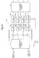
- FIG. 1illustrates a configuration of a digital receiver related to a first exemplary embodiment of the invention.
- a digital receiver 100includes an A/D converter 101, an A/D converter identification clock 102, a skew compensation filter 103, and a band compensation filter 104.
- the digital receiver 100further includes a filter coefficient setting circuit 105 related to the skew compensation filter, a filter coefficient setting circuit 106 related to the band compensation filter, and a digital signal processing circuit 107.
- FIG. 1when a plurality of units having the same function are arranged, notation for the units in the drawing is distinguished by adding "-1" and "-2" to reference numerals thereof. In following descriptions, if it is unnecessary to particularly distinguish them, for example, "A/D converter 101-1" and “A/D converter 101-2" are described as "A/D converter 101".
- a transmission signal transmitted from a transmitter which is not shownenters inputs (INI, IN2) of the digital receiver 100 through a transmission path which is not shown.
- the A/D converter 101converts signals, inputted in IN1 and IN2, which are analog electric signals into digital signals in synchronization with the A/D converter identification clock 102 connected thereto.
- the skew compensation filter 103conducts skew (phase) adjustment on the converted digital signals. At this time, a filter coefficient of the skew compensation filter 103 is set so that a desired amount of skew compensation is obtained, by the filter coefficient setting circuit 105 related to the skew compensation filter.
- band adjustmentis conducted with the band compensation filter 104.
- Outputs of the band compensation filter 104enter the digital signal processing circuit 107.
- the filter coefficient setting circuit 106sets a filter coefficient of the band compensation filter 104 so as to achieve a desired amount of band compensation.
- the digital receiver 100 shown in FIG. 1includes the A/D converter identification clocks 102, the skew compensation filters 103, the band compensation filters 104, the filter coefficient setting circuits 105 and the filter coefficient setting circuits 106 for 2 channels.
- An outputted signal from the band compensation filter 104 of each channelenters the digital signal processing circuit 107.
- FIG. 1illustrates 2 channels as the number of channels.
- the number of channels of the digital receiver 100is not limited to 2 channels.
- the digital signal processing circuit 107has to conduct signal processing while inputted signals of a plurality of channels are synchronized, that is, while no skew occurs between the channels.
- the skew differenceis compensated by using the skew compensation filter 103.
- FIG. 2is a diagram illustrating skew compensation using the liner interpolation method as an example of operation of the skew compensation filter 103 in detail.
- FIG. 2illustrates an example in which a sine wave is inputted as an input signal, A/D conversion is conducted with an oversampling frequency twice the frequency of the inputted sine wave, and skew (phase) of the channel 2 (Ch. 2) is compensated with reference to the channel 1 (Ch. 1).
- FIG. 2(a) , (A) illustrates an example of sample timing of an A/D converter in a reference lane (Ch. 1). (B) illustrates an example of ideal sample timing on Ch. 2. ⁇ x illustrates skew between Ch. 1 and Ch. 2. (C) in FIG. 2 illustrates an example of a sample point of Ch. 2, on which skew compensation is conducted.
- FIG. 2 (b)schematically illustrates linear interpolation of b(n) based on a(n) and a(n+1).
- FIG. 3is a diagram illustrating a configuration of a skew compensation filter employing the FIR filter.
- FIG. 3shows configurations of the skew compensation filter, in the following cases (a) the amount of skew compensation is -x sample (0 ⁇ x ⁇ 1) and (b) the amount of skew compensation is +x sample (0 ⁇ x ⁇ 1). In each case, if each tap coefficient is set appropriately, b (n) in the equation (1) can be calculated.
- FIG. 3illustrates an example of 3-tap FIR filter. A higher degree FIR filter may be employed in order to conduct wide range skew compensation.
- sampling rate of the A/D converter 101cannot be fully increased due to limit of operation speed and consumed power in a high-speed communication of more than 10G bps. Due to the limit, an over-sampling operation is usually conducted at one to two times a baud rate of a signal. As a result, the problem occurs that satisfactory filter characteristics are not obtained.
- FIG. 4is a diagram illustrating propagation characteristics of the skew compensation filter.
- FIG. 4illustrates an example of calculated propagation characteristics in performance of 64 GS/s (Giga-Sample per second) with respect to a signal with 32 Gb/s using the FIR filter shown in FIG. 3 . The example shows double over-sampling is performed.
- FIG. 4 (i) and FIG. 4 (ii)illustrate calculation results of propagation characteristics of FIR filter on the amount of skew compensation of 0.1 sample and the amount of skew compensation of 0.49 sample, respectively.
- a left axisrepresents amplitude characteristics (transit characteristics)
- a right axisrepresents group delay characteristics (amount of skew compensation).
- a frequency, at which 0.1 sample which is a desired amount of skew compensation as group delay is obtainedis around 10GHz or less.
- performance of a waveform distortion compensation filtermay be insufficient, because the amount of over-sample in the A/D converter 101 is insufficient.
- waveform distortionmay not be fully removed (compensated) or additional waveform distortion (deterioration of propagation characteristics) may further occur.
- the digital receiver of the first exemplary embodiment of the inventionfurther includes the band compensation filter 104 to solve the above problem.
- the digital receiver of the first exemplary embodimentcompensates deterioration of band characteristics due to the skew compensation filter 103 by using the band compensation filter 104 to achieve desired signal propagation characteristics.
- a method of skew compensation and an amount of skew compensationare determined, change of propagation characteristics due to the skew compensation filter 103 is determined uniquely. Therefore, when the band compensation filter 104 having propagation characteristics of suppressing propagation characteristics deterioration due to skew compensation is employed, it is possible to compensate additional waveform distortion which occurs in skew compensation filter 103.
- a filter which does not change group delay characteristics of the skew compensation filter 103, and only amplitude characteristics of which is opposite to the characteristics of the skew compensation filter 103may be employed as the band compensation filter 104.
- the band compensation filter 104may be configured by using the FIR filter.
- the filter coefficient setting circuit 106may calculate a filter coefficient by which desired characteristics opposite to characteristics of the skew compensation filter 103 is achieved in the band compensation filter 104.
- the set value of the band compensation filter 104may be set by referring to the look-up table which is calculated in advance based on the set value of the filter coefficient setting circuit 105.
- the set value of the filter coefficient setting circuit 106only has to be determined so that proper system performance is obtained by considering allowable circuit size and consumed power and performance required for a system, like band characteristics, group delay characteristics and the like.
- the set value of the filter coefficient setting circuit 106may be determined so that system performance, like an error rate, is optimized.
- the skew compensation filter 103 with a linear interpolation circuit in FIG. 3is one example of a skew compensation system, and other system is available as the skew compensation system.
- a method using a higher-order FIR filter or a method of conducting rate conversion by using up-sampling and an interpolation filtermay also conduct skew compensation.
- the digital receiver 100determines a set value of the filter coefficient setting circuit 107 by associating propagation characteristics of the skew compensation filter 103 with that of the band compensation filter and by considering circuit size and consumed power, and preferential performance (band characteristics, group delay characteristics) in the system. Thereby, a digital receiver with desired characteristics can be configured.
- the digital receiver of the first exemplary embodimentcan compensates additional waveform distortion which occurs in the skew compensation filter. Accordingly, the digital receiver of the first exemplary embodiment is well controllable and achieves distortion compensation with high performance and high accuracy.
- FIG. 5is a diagram illustrating a configuration of a digital receiver 500 of the second exemplary embodiment of the invention.
- the digital receiver 500includes a polarization diversity 90-degree hybrid 501, an optical-electric (O/E) converter 502, an A/D converter 503, a skew compensation filter 504 and a wavelength dispersion compensation filter 505.
- O/Eoptical-electric
- a DP-QPSK signal lightis a signal light transmitted from an optical transmitter which is not shown.
- the DP-QPSK signal light with waveform distortion due to wavelength dispersion of an optical fiber transmission pathis received by the digital receiver 500 of the invention.
- the received DP-QPSK signal lightis combined with a local oscillator light in the polarization diversity 90-degree hybrid 501 and is demodulated into 4 channels optical signals Ix, Qx, Iy, Qy.
- the 4 demodulated signals Ix, Qx, Iy, Qyare converted to electric signals by the O/E converters (optical electric converter) 502-1 to 502-4, respectively.
- the signals Ix, Qx, Iy, Qy, which have been converted to electric signals,are converted into digital signals by the following A/D converters 503-1 to 503-4, respectively.
- the skew compensation filter 504compensates skew between channels of signals converted to the digital signals.
- the wavelength dispersion compensation filter 505removes (compensates) waveform distortion which is included in the inputted signals and is caused by wavelength dispersion added in the optical transmission path. Outputs of the wavelength dispersion compensation filter 505 enter the digital signal processing circuit 508.
- the digital signal processing circuit 508gives, to the inputted signals, digital signal processing, like clock extraction, retiming, polarization tracking, local oscillator light phase estimation, and the like. Since the detailed processes in the digital signal processing circuit 508 has no relation with the invention and is described in Non-Patent Document 1 to be publicly known, descriptions thereof is omitted.
- the skew compensation filter 504 in the digital receiver 500 of the second exemplary embodiment of the inventionmay be the filter conducting linear interpolation, shown in FIG. 3 , just like the digital receiver 100 of the first exemplary embodiment of the invention.
- a filter which is configured by combining butterfly-typed FIR filters compensating crosstalk between the Ix (Iy) channel and the Qx (Qy) channel, as shown in FIG. 6may also be employed as the skew compensation filter 504.
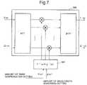
- FIG. 7is a diagram illustrating a configuration of the FDE (frequency domain equalization) wavelength dispersion compensation filter 505.
- the signals of I-ch and Q-chenter a FFT (fast Fourier transform) circuit and are converted into complex frequency region signals. Weighted multiplication is performed on signals converted to the complex frequency region signals by a set value of a filter coefficient of the filter coefficient setting circuit 507 related to the wavelength dispersion compensation filter, IFFT (inverse FFT) is further performed thereon, and the signals are converted into time domain signals and outputted.
- FFTfast Fourier transform
- the filter coefficient setting circuit 507calculates the product of the inverse function f -1 ( ⁇ ) of the function f ( ⁇ ) representing deterioration of propagation characteristic of the skew compensation filter 504 and the inverse function g -1 ( ⁇ ) of the propagation characteristics g ( ⁇ ) related to wavelength dispersion compensation, as a filter coefficient. Accordingly, it becomes possible to compensate waveform distortion added by the skew compensation filter 504 by using the wavelength dispersion compensation filter 505.
- the function f ( ⁇ ) representing deterioration of propagation characteristic of the skew compensation filter 504is a function extracting only amplitude characteristics (an absolute value of propagation characteristics of the skew compensation filter 504) of the graph in FIG. 4 .
- the DP-QPSK signalis exemplified as an input signal.
- the inventionmay be applied to a signal of various modulation systems, like ASK (amplitude shift keying), BPSK (binary PSK), SP (single polarization)-QPSK, OFDM (orthogonal frequency division multiplexing) signal.
- ASKamplitude shift keying
- BPSKbinary PSK
- SPsingle polarization
- OFDMorthogonal frequency division multiplexing
- the digital receiver of the second exemplary embodimentcalculates the product of the inverse function f -1 ( ⁇ ) of the function f ( ⁇ ) representing deterioration of propagation characteristic of the skew compensation filter and the inverse function g -1 ( ⁇ ) of the propagation characteristics g ( ⁇ ) related to wavelength dispersion compensation, as a filter coefficient.
- the digital receiver of the second exemplary embodimentcompensates waveform distortion added by the skew compensation filter by using the wavelength dispersion compensation filter. Accordingly, the digital receiver of the second exemplary embodiment is well controllable and achieves distortion compensation with high performance and high accuracy.
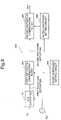
- FIG. 8is a diagram illustrating a digital filter 800 of the third exemplary embodiment of the invention.
- the digital filter 800includes an A/D converter 101, an A/D converter identification clock 102, a first distortion compensation filter 801 and a second distortion compensation filter 802.
- the digital filter 800further includes a filter coefficient setting circuit 803 related to the first distortion compensation filter and a filter coefficient setting circuit 804 related to the second distortion compensation filter.
- a signalwhich is received by a receiver through a transmission path and is O/E-converted, enters the A/D converter 101.
- the A/D converter 101converts the inputted signal, which is an analog electric signal, into a digital signal at the timing in synchronization with the A/D converter identification clock 102.
- the digital filter 800 of the third exemplary embodimentworks to associate propagation characteristics of the first distortion compensation filter with propagation characteristics of the second distortion compensation filter. As a result, even when it is difficult for the first distortion compensation filter alone to sufficiently achieve distortion compensation, the digital filter 800 is well-controllable and achieves distortion compensation with high performance and high accuracy.
- the first distortion compensation filter 801 and the second distortion compensation filter 802may not necessarily be separated filters in circuit implementation.
- the first distortion compensation filter 801 and the second distortion compensation filter 802may be configured as one high-order FIR filter.
- filter coefficient calculation on the filter coefficient setting circuit 803 and filter coefficient calculation on the filter coefficient setting circuit 804may be separated to set coefficients, based on the process equivalent to the above. Even if the first distortion compensation filter 801 and the second distortion compensation filter 802 is configured as one high-order FIR filter, controllability equivalent to that of the configuration including these filters separately is obtained by carrying out each filter coefficient calculation individually.
- the digital filter 800 without the A/D converter 101 and the A/D converter identification clock 102may compensate distortion of an inputted signal based on processes similar to the processes described in the third exemplary embodiment.
- the digital filter 800may be the configuration including only the first distortion compensation filter 801, the second distortion compensation filter 802, the filter coefficient setting circuit 803 related to the first distortion compensation filter and the filter coefficient setting circuit 804 related to the second distortion compensation filter.
- FIG. 9is a diagram illustrating a digital filter 900 of the modified example of the digital filter 800 related to the third exemplary embodiment of the invention.
- the digital filter 900includes a half fixed distortion compensation filter 901, an adaptive equalization distortion compensation filter 902, a filter coefficient setting circuit 903 related to the half fixed distortion compensation filter, a filter coefficient setting circuit 904 related to the adaptive equalization filter, a digital signal processing circuit 905 and a signal quality monitor 906.
- the digital filter 900differs from the digital filter 800 of the third exemplary embodiment of the invention in the configuration of the employed waveform distortion filter, and the other configuration thereof is similar to the configuration of the third exemplary embodiment. Therefore, the same reference numerals as those of the digital receiver 800 are given to the corresponding parts of the digital filter 900, and descriptions thereabout are omitted.
- the filter coefficient setting circuit 903sets the filter coefficient of the half fixed distortion compensation filter 901 based on compensation amount setting information.
- the adaptive equalization distortion compensation filter 902conducts adaptive equalization based on LMS (least mean square) algorithm or the like by using a decision feedback signal or a training signal or the like.
- the digital receiver 900may conduct adaptive equalization based on information of the signal quality monitor 906 like an error rate, a waveform monitor, or the like.
- filter coefficient calculation of the filter coefficient setting circuit 904is conducted based on setting information set by the filter coefficient setting circuit 903, by preliminarily considering, aside from adaptive equalization, additional fixed distortion due to the half fixed distortion compensation filter 901, convergence and controllability of adaptive equalization can be improved.
- Waveform distortion which can be compensated by the half fixed distortion compensation filter 901is, for example, waveform distortion in the transmitter, the transmission path, and the optical front-end part (each not shown) and distortion due to calibration error on the A/D converter 101.
- the present modified examplemay be applied to compensation for distortion due to a band limitation filter of a duo-binary modulation system, distortion due to a conversion filter from a RZ (return-to-zero) signal to a NRZ (non-RZ) signal, and the like.
- the digital filter device of the second modified example of the third exemplary embodimentis well controllable and achieves distortion compensation with high performance and high accuracy.
- each exemplary embodiment described abovemay be achieved by a computer.
- the digital receiver or the digital filter device in each exemplary embodimentmay include a central processing unit and memory.
- the central processing unitmay achieve the function of the digital receiver or the digital filter device in each exemplary embodiment by executing a program stored in the memory.
Landscapes
- Engineering & Computer Science (AREA)
- Computer Networks & Wireless Communication (AREA)
- Signal Processing (AREA)
- Power Engineering (AREA)
- Physics & Mathematics (AREA)
- Computer Hardware Design (AREA)
- Mathematical Physics (AREA)
- Electromagnetism (AREA)
- Optical Communication System (AREA)
- Cable Transmission Systems, Equalization Of Radio And Reduction Of Echo (AREA)
Description
- The invention relates to a digital filter device, a digital filtering method and a control program of the digital filter device which are employed in a digital coherent optical communication.
- In these days, importance of a digital coherent optical communication technology is increasing, as a demand for a network with high speed and large capacity is increasing. A digital coherent reception system is also called an intradyne reception system. The digital coherent reception system can achieve receiving sensitivity improvement of 3 dB to 6 dB or more, compared with a modulation system, like OOK(on-off keying) and DPSK(differential quadrature phase shift keying). The digital coherent reception system advantageously has high compatibility with a multi-level modulation system, like a polarization multiplexing system and QAM (quadrature amplitude modulation).
FIG. 10 is a diagram illustrating a configuration of a digitalcoherent receiver 400 described inPatent Document 1 andNon-Patent Document 1. A signal light entering the digital coherent receiver is a multiplexed signal (DP-QPSK signal light) with 4 channels (Ix, Qx, Iy, Qy) using a Polarization multiplexing (DP:dual-polarization)-QPSK(quadrature phase shift keying) signal.- The DP-QPSK signal is separated to each channel of Ix, Qx, Iy, and Qy at a polarization diversity 90-
degree hybrid 401. The separated signals are converted into analog electric signals per channel at respective optical-electric (O/E) converters 402-1 to 402-4. Respective O/E-converted signals are converted into digital signals at respective A/D (analog to digital) converters 403-1 to 403-4 which carry out sampling in synchronization with a reference sampling clock (CLK) 405. - The digital signals converted by the A/D converters 403-1 to 403-4 enter a digital
signal processing circuit 404. A background of why the digitalsignal processing circuit 404 is employed in the digital coherent reception system and a function of the digitalsignal processing circuit 404 are described below. - The coherent receiver which does not carry out digital signal processing includes a problem that it is difficult to keep stable reception due to off-set of a frequency and a phase of a LO (local oscillator) light and polarization fluctuation.
- In the meantime, as an electronic device technology improves, it has become possible to use a high-speed A/D converter for signal processing of a high-speed communication device. As a result, by carrying out digital signal processing for a signal converted to a digital signal, it has become possible to compensate off-set of a frequency and a phase of a LO light which has been a problem of the coherent reception system which does not carry out digital signal processing. The digital signal processing enables to compensate polarization fluctuation of an optical signal.
- As described above, the digital coherent reception system achieves stable and accurate coherent reception compared with the coherent reception system which does not carry out digital signal processing.
- Furthermore, in the digital coherent reception system, it is possible to add compensation of wavelength dispersion and high waveform equalization to a signal in addition to compensation of offset of a frequency and a phase and compensation of polarization fluctuation.
- Non-Patent
Document 2 describes a skew compensation technology that is a technology for compensating waveform distortion used in the digital coherent receiver. Non-PatentDocument 2 describes the technology which achieves highly accurate skew compensation through quadratic function approximation on adjacent sampling points and sampling points before and behind the adjacent sampling points by using FIR (finite impulse response) filter. - Since a high-speed A/D converter becomes widespread, in backplane transmission which connects circuit substrates to each other, it becomes possible to conduct high-level waveform equalization and highly accurate digital clock extraction, like MLSE (most likelihood sequence estimation) using digital signal processing or the like, in order to tackle the problem of interference between codes and deterioration of jitter characteristics due to band shortage of a transmission path.
- Patent Document:
JP2008-205654 A - Non-patent Document 1:
Seb J. Savory, "Digital filters for coherent optical receivers," Optics Express Vol. 16, No. 2, p. 804-817 (Jan. 2008) - Non-Patent Document 2:
Tanimura et al, "A Simple Digital Skew Compensator for Coherent Receiver," in Proceedings of European Conference and Exhibition on Optical Communication (ECOC) 2009, Vienna, Austria, paper 7.3.2 (2009) US 2009/190647 A1 relates to a distortion compensating apparatus having an adaptive distortion compensating unit to compensate nonlinear distortion.- In digital signal processing for an ultrahigh-speed signal of more than tens of GS/s (samples per second), a sampling rate of an A/D converter cannot be fully increased because of the limit of operation speed and consumed power of the A/D converter. Due to the limit, an over-sampling operation is usually conducted at the rate of a baud rate of the signal or at most twice the rate thereof. As a result, in digital signal processing for an ultrahigh-speed signal, a distortion compensation filter for compensating various waveform distortions has difficulty in obtaining sufficient characteristics.
- In next generation optical communication system in which a transmission rate is more than 100 Gb/s (gigabit per second), a multiplexed signal with 4 channels using DP-QPSK illustrated in
FIG. 10 may be employed. In the DP-QPSK system, skew (propagation delay difference) is generated between channels due to phase shift which occurs at an optical front end section, like 90-degree hybrid, TIA (transimpedance amplifier) and the like, and due to group delay characteristics. The skew which is generated between channels deteriorates performance of the system. The skew of the DP-QPSK signal, therefore, has to be compensated with high accuracy by using a distortion compensation filter. - An object of the invention is to provide a digital filter device to solve the problem of achieving highly accurate distortion compensation.
- The present invention is defined by the attached independent claims. Other preferred embodiments may be found in the dependent claims.
- The present application discloses a digital filter device, comprising:first distortion compensation filter means (801) for conducting distortion compensation of first waveform distortion included in an inputted signal through digital signal processing;first filter coefficient setting means (803) for setting a filter coefficient of the first distortion compensation filter means (801);second distortion compensation filter means (802) for compensating second waveform distortion included in a signal outputted from the first distortion compensation filter means (801);second filter coefficient setting means (804) for setting a filter coefficient of the second distortion compensation filter means (802) based on the filter coefficient set by the first filter coefficient setting means (803); and A/D conversion means (101) for converting an inputted analog signal into a digital signal and inputting the converted digital signal into the first distortion compensation filter means (801),wherein an output of the A/D conversion means (101) enters the first distortion compensation filter means (801). Furthermore the present application discloses a digital filtering method, comprising setting a filter coefficient of first distortion compensation filter means (801); compensating distortion of first waveform distortion included in an inputted signal; setting a filter coefficient of second distortion compensation filter means (802) based on the filter coefficient of the first distortion compensation filter means (801); compensating second waveform distortion included in a signal outputted from the first distortion compensation filter means (801); and converting, by A/D conversion means (101), an inputted analog signal into a digital signal and inputting the converted digital signal into the first distortion compensation filter means (801), wherein an output of the A/ D conversion means (101) enters the first distortion compensation filter means (801). Furthermore the present application discloses a control program of a digital filter device causing a computer of the digital filter device to function as:first distortion compensation filter means (801) for conducting distortion compensation of first waveform distortion included in an inputted signal through digital signal processing;first filter coefficient setting means (803) for setting a filter coefficient of the first distortion compensation filter means (801);second distortion compensation filter means (802) for compensating second waveform distortion included in a signal outputted from the first distortion compensation filter means (801);second filter coefficient setting means (804) for setting a filter coefficient of the second distortion compensation filter means (802) based on the filter coefficient set by the first filter coefficient setting means (803); andA/D conversion means (101) for converting an inputted analog signal into a digital signal and inputting the converted digital signal into the first distortion compensation filter means (801),wherein an output of the A/D conversion means (101) enters the first distortion compensation filter means (801).
- The digital filter device of the invention includes advantage of achieving distortion compensation with advanced controllability, high performance and high accuracy.
FIG. 1 is a diagram illustrating a configuration of a digital receiver related to a first exemplary embodiment of the invention.FIG. 2 is a diagram illustrating skew compensation using a linear interpolation method in detail.FIG. 3 is a diagram illustrating a configuration of a skew compensation filter employing a FIR filter.FIG. 4 is a diagram illustrating propagation characteristics of the skew compensation filter.FIG. 5 is a diagram illustrating a configuration of a digital receiver related to a second exemplary embodiment of the invention.FIG. 6 is a block diagram illustrating a schematic configuration of the skew compensation filter.FIG. 7 is a diagram illustrating a configuration of a wavelength dispersion compensation filter based on frequency region waveform equalization.FIG. 8 is a diagram illustrating a configuration of a digital receiver related to a third exemplary embodiment of the invention.FIG. 9 is a diagram illustrating modified example of the configuration of the digital receiver related to the third exemplary embodiment of the invention.FIG. 10 is a diagram illustrating a configuration of a digital coherent receiver related to the invention.- Exemplary embodiments of the invention are described in detail with reference to drawings.
FIG. 1 illustrates a configuration of a digital receiver related to a first exemplary embodiment of the invention. InFIG. 1 , adigital receiver 100 includes an A/D converter 101, an A/Dconverter identification clock 102, a skew compensation filter 103, and a band compensation filter 104. Thedigital receiver 100 further includes a filter coefficient setting circuit 105 related to the skew compensation filter, a filter coefficient setting circuit 106 related to the band compensation filter, and a digitalsignal processing circuit 107. InFIG. 1 , when a plurality of units having the same function are arranged, notation for the units in the drawing is distinguished by adding "-1" and "-2" to reference numerals thereof. In following descriptions, if it is unnecessary to particularly distinguish them, for example, "A/D converter 101-1" and "A/D converter 101-2" are described as "A/D converter 101".- An operation of the
digital receiver 100 related to the first exemplary embodiment of the invention is described below. A transmission signal transmitted from a transmitter which is not shown enters inputs (INI, IN2) of thedigital receiver 100 through a transmission path which is not shown. The A/D converter 101 converts signals, inputted in IN1 and IN2, which are analog electric signals into digital signals in synchronization with the A/Dconverter identification clock 102 connected thereto. The skew compensation filter 103 conducts skew (phase) adjustment on the converted digital signals. At this time, a filter coefficient of the skew compensation filter 103 is set so that a desired amount of skew compensation is obtained, by the filter coefficient setting circuit 105 related to the skew compensation filter. - Next, with respect to signals, skew of which is compensated, band adjustment is conducted with the band compensation filter 104. Outputs of the band compensation filter 104 enter the digital
signal processing circuit 107. The filter coefficient setting circuit 106 sets a filter coefficient of the band compensation filter 104 so as to achieve a desired amount of band compensation. - The
digital receiver 100 shown inFIG. 1 includes the A/D converter identification clocks 102, the skew compensation filters 103, the band compensation filters 104, the filter coefficient setting circuits 105 and the filter coefficient setting circuits 106 for 2 channels. An outputted signal from the band compensation filter 104 of each channel enters the digitalsignal processing circuit 107. - Using the inputted digital signals of 2 channels, the digital
signal processing circuit 107 removes (compensate) waveform distortion included in the signals and demodulates data.FIG. 1 illustrates 2 channels as the number of channels. The number of channels of thedigital receiver 100 is not limited to 2 channels. The digitalsignal processing circuit 107 has to conduct signal processing while inputted signals of a plurality of channels are synchronized, that is, while no skew occurs between the channels. When skew between the channels exists in a signal which enters thedigital receiver 100, or when phase shift exists in identification timing of the A/Dconverter identification clock 102, the skew difference is compensated by using the skew compensation filter 103. FIG. 2 is a diagram illustrating skew compensation using the liner interpolation method as an example of operation of the skew compensation filter 103 in detail.FIG. 2 illustrates an example in which a sine wave is inputted as an input signal, A/D conversion is conducted with an oversampling frequency twice the frequency of the inputted sine wave, and skew (phase) of the channel 2 (Ch. 2) is compensated with reference to the channel 1 (Ch. 1).- In
FIG. 2 (a) , (A) illustrates an example of sample timing of an A/D converter in a reference lane (Ch. 1). (B) illustrates an example of ideal sample timing on Ch. 2. Δx illustrates skew between Ch. 1 and Ch. 2. (C) inFIG. 2 illustrates an example of a sample point of Ch. 2, on which skew compensation is conducted. - In the skew compensation based on the linear interpolation method, if a sample point value of the
channel 2 before skew compensation is described as a (n) and the amount of skew compensation is described as Δx (unit: sample=1/fs), a sample point value b(n) of thechannel 2 after skew compensation is given by the following equation,
FIG. 2 (b) schematically illustrates linear interpolation of b(n) based on a(n) and a(n+1). - A circuit having a FIR (finite impulse response) filter is known as a filter circuit achieving the linear interpolation.
FIG. 3 is a diagram illustrating a configuration of a skew compensation filter employing the FIR filter. FIG. 3 shows configurations of the skew compensation filter, in the following cases (a) the amount of skew compensation is -x sample (0<x<1) and (b) the amount of skew compensation is +x sample (0<x<1). In each case, if each tap coefficient is set appropriately, b (n) in the equation (1) can be calculated.FIG. 3 illustrates an example of 3-tap FIR filter. A higher degree FIR filter may be employed in order to conduct wide range skew compensation.- The problem which occurs when skew compensation using linear interpolation is conducted is that sampling rate of the A/
D converter 101 cannot be fully increased due to limit of operation speed and consumed power in a high-speed communication of more than 10G bps. Due to the limit, an over-sampling operation is usually conducted at one to two times a baud rate of a signal. As a result, the problem occurs that satisfactory filter characteristics are not obtained. FIG. 4 is a diagram illustrating propagation characteristics of the skew compensation filter.FIG. 4 illustrates an example of calculated propagation characteristics in performance of 64 GS/s (Giga-Sample per second) with respect to a signal with 32 Gb/s using the FIR filter shown inFIG. 3 . The example shows double over-sampling is performed.FIG. 4 (i) and FIG. 4 (ii) illustrate calculation results of propagation characteristics of FIR filter on the amount of skew compensation of 0.1 sample and the amount of skew compensation of 0.49 sample, respectively. InFIG. 4 , a left axis represents amplitude characteristics (transit characteristics), and a right axis represents group delay characteristics (amount of skew compensation).- As shown in
FIG. 4 (i) , when the amount of skew compensation is 0.1 sample, attenuation of amplitude characteristics is small even in a high-frequency (e.g. around 20 GHz) region (around 1.2 dB at 20 GHz, inFIG. 4 ). On the contrary, inFIG. 4 (i) , a frequency, at which 0.1 sample which is a desired amount of skew compensation as group delay is obtained, is around 10GHz or less. - As shown in
FIG. 4 (ii) , when the amount of skew compensation is 0.49 sample, amplitude is attenuated by about 5 dB in around 20 GHz. On the contrary, inFIG. 4 (ii) , desired performance of 0.49 sample is obtained up to around 20 GHz with respect to group delay (amount of skew compensation). - As described above, in the high-speed digital communication, performance of a waveform distortion compensation filter, like the skew compensation filter 104, may be insufficient, because the amount of over-sample in the A/
D converter 101 is insufficient. In the skew compensation filter 104, therefore, waveform distortion may not be fully removed (compensated) or additional waveform distortion (deterioration of propagation characteristics) may further occur. - Furthermore, when the set value of the filter coefficient setting circuit 105 in the skew compensation filter 103 (e.g. amount of skew compensation (amount of group delay) in
FIG. 4 ) is modified, other propagation characteristics (e.g. amplitude characteristics (transit characteristics) inFIG. 4 ) also changes. Therefore, stable system performance is not obtained. - The digital receiver of the first exemplary embodiment of the invention further includes the band compensation filter 104 to solve the above problem. The digital receiver of the first exemplary embodiment compensates deterioration of band characteristics due to the skew compensation filter 103 by using the band compensation filter 104 to achieve desired signal propagation characteristics.
- If a method of skew compensation and an amount of skew compensation are determined, change of propagation characteristics due to the skew compensation filter 103 is determined uniquely. Therefore, when the band compensation filter 104 having propagation characteristics of suppressing propagation characteristics deterioration due to skew compensation is employed, it is possible to compensate additional waveform distortion which occurs in skew compensation filter 103. For example, a filter which does not change group delay characteristics of the skew compensation filter 103, and only amplitude characteristics of which is opposite to the characteristics of the skew compensation filter 103, may be employed as the band compensation filter 104. The band compensation filter 104 may be configured by using the FIR filter. The filter coefficient setting circuit 106 may calculate a filter coefficient by which desired characteristics opposite to characteristics of the skew compensation filter 103 is achieved in the band compensation filter 104. In the filter coefficient setting circuit 106, the set value of the band compensation filter 104 may be set by referring to the look-up table which is calculated in advance based on the set value of the filter coefficient setting circuit 105.
- Deterioration of propagation characteristics which occurs in the skew compensation filter 103 does not need to be fully compensated. The set value of the filter coefficient setting circuit 106 only has to be determined so that proper system performance is obtained by considering allowable circuit size and consumed power and performance required for a system, like band characteristics, group delay characteristics and the like. The set value of the filter coefficient setting circuit 106 may be determined so that system performance, like an error rate, is optimized.
- The skew compensation filter 103 with a linear interpolation circuit in
FIG. 3 is one example of a skew compensation system, and other system is available as the skew compensation system. For example, a method using a higher-order FIR filter or a method of conducting rate conversion by using up-sampling and an interpolation filter may also conduct skew compensation. In both cases, thedigital receiver 100 determines a set value of the filtercoefficient setting circuit 107 by associating propagation characteristics of the skew compensation filter 103 with that of the band compensation filter and by considering circuit size and consumed power, and preferential performance (band characteristics, group delay characteristics) in the system. Thereby, a digital receiver with desired characteristics can be configured. - Including the band compensation filter with propagation characteristics of suppressing change of propagation characteristics due to the skew compensation filter, the digital receiver of the first exemplary embodiment can compensates additional waveform distortion which occurs in the skew compensation filter. Accordingly, the digital receiver of the first exemplary embodiment is well controllable and achieves distortion compensation with high performance and high accuracy.
- Next, a second exemplary embodiment of the invention is described below.
FIG. 5 is a diagram illustrating a configuration of adigital receiver 500 of the second exemplary embodiment of the invention. InFIG. 5 , thedigital receiver 500 includes a polarization diversity 90-degree hybrid 501, an optical-electric (O/E) converter 502, an A/D converter 503, askew compensation filter 504 and a wavelengthdispersion compensation filter 505. - The
digital receiver 500 further includes a filtercoefficient setting circuit 506 related to the skew compensation filter, a filtercoefficient setting circuit 507 related to the wavelength dispersion filter, and a digitalsignal processing circuit 508. - In
FIG. 5 , when a plurality of units having the same function are arranged, the units are distinguished by adding "-1" and "-2" to reference numerals thereof. In following descriptions, if it is unnecessary to particularly distinguish them, for example, "O/E converter 502-1" and "O/E converter 502-2" are described as "O/E converter 502". - An operation of the
digital receiver 500 related to the second exemplary embodiment of the invention is described. InFIG. 5 , a DP-QPSK signal light is a signal light transmitted from an optical transmitter which is not shown. The DP-QPSK signal light with waveform distortion due to wavelength dispersion of an optical fiber transmission path is received by thedigital receiver 500 of the invention. The received DP-QPSK signal light is combined with a local oscillator light in the polarization diversity 90-degree hybrid 501 and is demodulated into 4 channels optical signals Ix, Qx, Iy, Qy. - The 4 demodulated signals Ix, Qx, Iy, Qy are converted to electric signals by the O/E converters (optical electric converter) 502-1 to 502-4, respectively. The signals Ix, Qx, Iy, Qy, which have been converted to electric signals, are converted into digital signals by the following A/D converters 503-1 to 503-4, respectively.
- The
skew compensation filter 504 compensates skew between channels of signals converted to the digital signals. The x polarization signals (Ix, Qx) and the y polarization signals (Iy, Qy), skew of which are compensated, enter the wavelength dispersion compensation filters 505-1 and 505-2, respectively. - The wavelength
dispersion compensation filter 505 removes (compensates) waveform distortion which is included in the inputted signals and is caused by wavelength dispersion added in the optical transmission path. Outputs of the wavelengthdispersion compensation filter 505 enter the digitalsignal processing circuit 508. The digitalsignal processing circuit 508 gives, to the inputted signals, digital signal processing, like clock extraction, retiming, polarization tracking, local oscillator light phase estimation, and the like. Since the detailed processes in the digitalsignal processing circuit 508 has no relation with the invention and is described inNon-Patent Document 1 to be publicly known, descriptions thereof is omitted. - The
skew compensation filter 504 in thedigital receiver 500 of the second exemplary embodiment of the invention may be the filter conducting linear interpolation, shown inFIG. 3 , just like thedigital receiver 100 of the first exemplary embodiment of the invention. Or a filter which is configured by combining butterfly-typed FIR filters compensating crosstalk between the Ix (Iy) channel and the Qx (Qy) channel, as shown inFIG. 6 , may also be employed as theskew compensation filter 504. FIG. 7 is a diagram illustrating a configuration of the FDE (frequency domain equalization) wavelengthdispersion compensation filter 505. InFIG. 7 , the signals of I-ch and Q-ch enter a FFT (fast Fourier transform) circuit and are converted into complex frequency region signals. Weighted multiplication is performed on signals converted to the complex frequency region signals by a set value of a filter coefficient of the filtercoefficient setting circuit 507 related to the wavelength dispersion compensation filter, IFFT (inverse FFT) is further performed thereon, and the signals are converted into time domain signals and outputted.- The filter
coefficient setting circuit 507 calculates the product of the inverse function f-1 (ω) of the function f (ω) representing deterioration of propagation characteristic of theskew compensation filter 504 and the inverse function g-1 (ω) of the propagation characteristics g (ω) related to wavelength dispersion compensation, as a filter coefficient. Accordingly, it becomes possible to compensate waveform distortion added by theskew compensation filter 504 by using the wavelengthdispersion compensation filter 505. The function f (ω) representing deterioration of propagation characteristic of theskew compensation filter 504 is a function extracting only amplitude characteristics (an absolute value of propagation characteristics of the skew compensation filter 504) of the graph inFIG. 4 . - The wavelength
dispersion compensation filter 505 does not need to fully compensate deterioration of propagation characteristics occurred in theskew compensation filter 504, just like thedigital receiver 100 of the first exemplary embodiment of the invention. A set value of the filtercoefficient setting circuit 507 may be determined so that specifications suitable for the system are satisfied, based on circuit size and consumed power allowable for thedigital receiver 500 and band characteristics and group delay characteristics allowable for the system. - In the above exemplary embodiment, the DP-QPSK signal is exemplified as an input signal. The invention may be applied to a signal of various modulation systems, like ASK (amplitude shift keying), BPSK (binary PSK), SP (single polarization)-QPSK, OFDM (orthogonal frequency division multiplexing) signal.
- As described above, the digital receiver of the second exemplary embodiment calculates the product of the inverse function f-1 (ω) of the function f (ω) representing deterioration of propagation characteristic of the skew compensation filter and the inverse function g-1 (ω) of the propagation characteristics g (ω) related to wavelength dispersion compensation, as a filter coefficient. The digital receiver of the second exemplary embodiment compensates waveform distortion added by the skew compensation filter by using the wavelength dispersion compensation filter. Accordingly, the digital receiver of the second exemplary embodiment is well controllable and achieves distortion compensation with high performance and high accuracy.
- Next, a third exemplary embodiment of the invention is described.
FIG. 8 is a diagram illustrating adigital filter 800 of the third exemplary embodiment of the invention. InFIG. 8 , thedigital filter 800 includes an A/D converter 101, an A/Dconverter identification clock 102, a firstdistortion compensation filter 801 and a seconddistortion compensation filter 802. Thedigital filter 800 further includes a filtercoefficient setting circuit 803 related to the first distortion compensation filter and a filtercoefficient setting circuit 804 related to the second distortion compensation filter. - An operation of the
digital filter 800 is described below. In thedigital filter 800 shown inFIG. 8 , a signal, which is received by a receiver through a transmission path and is O/E-converted, enters the A/D converter 101. The A/D converter 101 converts the inputted signal, which is an analog electric signal, into a digital signal at the timing in synchronization with the A/Dconverter identification clock 102. - The first
distortion compensation filter 801 is a filter which conducts waveform distortion compensation of first waveform distortion which is added to a signal at a transmitter, a transmission path, an optical front-end part, the A/D converter 101, and the like, based on a filter set value of the filtercoefficient setting circuit 803 related to the first distortion compensation filter. In high-speed digital communication, however, sufficient compensation performance may not be obtained in the firstdistortion compensation filter 801. In this case, output of the firstdistortion compensation filter 801 includes second waveform distortion including residual waveform distortion which the firstdistortion compensation filter 801 cannot remove (compensate) and waveform distortion which is added by the firstdistortion compensation filter 801. The filtercoefficient setting circuit 804 installs, into the seconddistortion compensation filter 802, a filter coefficient to achieve propagation characteristics suppressing change of propagation characteristics which additionally occurs at the firstdistortion compensation filter 801, based on set information of the filtercoefficient setting circuit 803. - The
digital filter 800 of the third exemplary embodiment works to associate propagation characteristics of the first distortion compensation filter with propagation characteristics of the second distortion compensation filter. As a result, even when it is difficult for the first distortion compensation filter alone to sufficiently achieve distortion compensation, thedigital filter 800 is well-controllable and achieves distortion compensation with high performance and high accuracy. - The first
distortion compensation filter 801 and the seconddistortion compensation filter 802 may not necessarily be separated filters in circuit implementation. For example, the firstdistortion compensation filter 801 and the seconddistortion compensation filter 802 may be configured as one high-order FIR filter. In this case, filter coefficient calculation on the filtercoefficient setting circuit 803 and filter coefficient calculation on the filtercoefficient setting circuit 804 may be separated to set coefficients, based on the process equivalent to the above. Even if the firstdistortion compensation filter 801 and the seconddistortion compensation filter 802 is configured as one high-order FIR filter, controllability equivalent to that of the configuration including these filters separately is obtained by carrying out each filter coefficient calculation individually. - In
FIG. 8 , thedigital filter 800 without the A/D converter 101 and the A/Dconverter identification clock 102 may compensate distortion of an inputted signal based on processes similar to the processes described in the third exemplary embodiment. - That is, the
digital filter 800 may be the configuration including only the firstdistortion compensation filter 801, the seconddistortion compensation filter 802, the filtercoefficient setting circuit 803 related to the first distortion compensation filter and the filtercoefficient setting circuit 804 related to the second distortion compensation filter. - In this configuration, it is possible to operate the
digital filter 800 so as to associate propagation characteristics of the firstdistortion compensation filter 801 with propagation characteristics of the seconddistortion compensation filter 802 based on processes similar to the processes described in the third exemplary embodiment. Even if the A/D converter and the A/D converter identification clock are not included, the digital filter of the first modified example of the third exemplary embodiment is well controllable and achieves distortion compensation with high performance and high accuracy. FIG. 9 is a diagram illustrating adigital filter 900 of the modified example of thedigital filter 800 related to the third exemplary embodiment of the invention. InFIG. 9 , thedigital filter 900 includes a half fixeddistortion compensation filter 901, an adaptive equalizationdistortion compensation filter 902, a filtercoefficient setting circuit 903 related to the half fixed distortion compensation filter, a filtercoefficient setting circuit 904 related to the adaptive equalization filter, a digitalsignal processing circuit 905 and asignal quality monitor 906.- The
digital filter 900 differs from thedigital filter 800 of the third exemplary embodiment of the invention in the configuration of the employed waveform distortion filter, and the other configuration thereof is similar to the configuration of the third exemplary embodiment. Therefore, the same reference numerals as those of thedigital receiver 800 are given to the corresponding parts of thedigital filter 900, and descriptions thereabout are omitted. - Operations of the
digital filter 900 are described below. InFIG. 9 , the filtercoefficient setting circuit 903 sets the filter coefficient of the half fixeddistortion compensation filter 901 based on compensation amount setting information. The adaptive equalizationdistortion compensation filter 902 conducts adaptive equalization based on LMS (least mean square) algorithm or the like by using a decision feedback signal or a training signal or the like. Thedigital receiver 900 may conduct adaptive equalization based on information of the signal quality monitor 906 like an error rate, a waveform monitor, or the like. In this case, if filter coefficient calculation of the filtercoefficient setting circuit 904 is conducted based on setting information set by the filtercoefficient setting circuit 903, by preliminarily considering, aside from adaptive equalization, additional fixed distortion due to the half fixeddistortion compensation filter 901, convergence and controllability of adaptive equalization can be improved. - Waveform distortion which can be compensated by the half fixed
distortion compensation filter 901 is, for example, waveform distortion in the transmitter, the transmission path, and the optical front-end part (each not shown) and distortion due to calibration error on the A/D converter 101. The present modified example may be applied to compensation for distortion due to a band limitation filter of a duo-binary modulation system, distortion due to a conversion filter from a RZ (return-to-zero) signal to a NRZ (non-RZ) signal, and the like. - The digital filter device of the second modified example of the third exemplary embodiment is well controllable and achieves distortion compensation with high performance and high accuracy.
- The function of each exemplary embodiment described above may be achieved by a computer. The digital receiver or the digital filter device in each exemplary embodiment may include a central processing unit and memory. The central processing unit may achieve the function of the digital receiver or the digital filter device in each exemplary embodiment by executing a program stored in the memory.
- While the invention has been particularly shown and described with reference to exemplary embodiments thereof, the invention is not limited to these embodiments. It will be understood by those of ordinary skill in the art that various changes in form and details may be made therein without departing from the scope of the present invention as defined by the claims.
- This application is based upon and claims the benefit of priority from
Japanese patent application No. 2010-195370 filed on September 1, 2010 - 100, 500, 800, 900
- digital receiver
- 101
- A/D converter
- 102
- A/D converter identification clock
- 103
- skew compensation filter
- 104
- band compensation filter
- 105
- filter coefficient setting circuit
- 106
- filter coefficient setting circuit
- 107
- digital signal processing circuit
- 400
- digital coherent receiver
- 401
- polarization diversity 90-degree hybrid
- 402
- O/E converter
- 403
- A/D converter
- 404
- digital signal processing circuit
- 405
- reference sampling clock
- 501
- polarization diversity 90-degree hybrid
- 502
- O/E converter
- 503
- A/D converter
- 504
- skew compensation filter
- 505
- wavelength dispersion compensation circuit
- 506
- filter coefficient setting circuit
- 507
- filter coefficient setting circuit
- 508
- digital signal processing circuit
- 801
- first distortion compensation filter
- 802
- second distortion compensation filter
- 803
- filter coefficient setting circuit
- 804
- filter coefficient setting circuit
- 901
- half fixed distortion compensation filter
- 902
- adaptive equalization distortion compensation circuit
- 903
- filter coefficient setting circuit
- 904
- filter coefficient setting circuit
- 905
- digital signal processing circuit
- 906
- signal quality monitor

Claims (9)
- A digital filter device, comprising:first distortion compensation filter means (801) for conducting distortion compensation of first waveform distortion included in an inputted signal through digital signal processing;first filter coefficient setting means (803) for setting a filter coefficient of the first distortion compensation filter means (801);second distortion compensation filter means (802) for compensating second waveform distortion included in a signal outputted from the first distortion compensation filter means (801);second filter coefficient setting means (804) for setting a filter coefficient of the second distortion compensation filter means (802) based on the filter coefficient set by the first filter coefficient setting means (803); andA/D conversion means (101) for converting an inputted analog signal into a digital signal and inputting the converted digital signal into the first distortion compensation filter means (801),wherein an output of the A/D conversion means (101) enters the first distortion compensation filter means (801).
- The digital filter device of claim 1, wherein the second filter coefficient setting means (804) sets the filter coefficient of the second distortion compensation filter means (802) so as to suppress change of propagation characteristics caused by the first distortion compensation filter (801).
- The digital filter device of claim 1, wherein the second filter coefficient setting means (804) sets the filter coefficient of the second distortion compensation filter means (802) so as to suppress change of amplitude characteristics caused by the first distortion compensation filter means (801).
- The digital filter device of any one of claim 1 to claim 3, wherein the first distortion compensation filter means (801) is skew compensation means (103) for compensating skew of an inputted signal.
- The digital filter device of claim 4, wherein the skew compensation means (103) includes a finite impulse response, FIR, filter and wherein the first filter coefficient setting means (803) calculates a filter coefficient of the FIR filter in response to predetermined skew compensation characteristics.
- The digital filter device of any one of claim 1 to claim 5, wherein the second distortion compensation filter means (802) includes a frequency domain equalization circuit (505).
- The digital filter device of any one of claim 1 to claim 6, further comprising:digital signal processing means (905) for digitally processing a signal outputted from the second distortion compensation filter means (802); andsignal quality monitor means (906) for monitoring quality of a signal outputted from the digital signal processing means (905), wherein the second filter coefficient setting means (804) determines the filter coefficient of the second distortion compensation filter means (802) based on a monitoring result of the signal quality monitor.
- A digital filtering method, comprisingsetting a filter coefficient of first distortion compensation filter means (801);compensating distortion of first waveform distortion included in an inputted signal;setting a filter coefficient of second distortion compensation filter means (802) based on the filter coefficient of the first distortion compensation filter means (801);compensating second waveform distortion included in a signal outputted from the first distortion compensation filter means (801); andconverting, by A/D conversion means (101), an inputted analog signal into a digital signal and inputting the converted digital signal into the first distortion compensation filter means (801),wherein an output of the A/D conversion means (101) enters the first distortion compensation filter means (801).
- A control program of a digital filter device causing a computer of the digital filter device to function as:first distortion compensation filter means (801) for conducting distortion compensation of first waveform distortion included in an inputted signal through digital signal processing;first filter coefficient setting means (803) for setting a filter coefficient of the first distortion compensation filter means (801);second distortion compensation filter means (802) for compensating second waveform distortion included in a signal outputted from the first distortion compensation filter means (801);second filter coefficient setting means (804) for setting a filter coefficient of the second distortion compensation filter means (802) based on the filter coefficient set by the first filter coefficient setting means (803); andA/D conversion means (101) for converting an inputted analog signal into a digital signal and inputting the converted digital signal into the first distortion compensation filter means (801),wherein an output of the A/D conversion means (101) enters the first distortion compensation filter means (801).
Applications Claiming Priority (2)
| Application Number | Priority Date | Filing Date | Title |
|---|---|---|---|
| JP2010195370 | 2010-09-01 | ||
| PCT/JP2011/069103WO2012029613A1 (en) | 2010-09-01 | 2011-08-18 | Digital filter device, digital filtering method, and control program for digital filter device |
Publications (3)
| Publication Number | Publication Date |
|---|---|
| EP2613452A1 EP2613452A1 (en) | 2013-07-10 |
| EP2613452A4 EP2613452A4 (en) | 2016-12-21 |
| EP2613452B1true EP2613452B1 (en) | 2022-12-28 |
Family
ID=45772705
Family Applications (1)
| Application Number | Title | Priority Date | Filing Date |
|---|---|---|---|
| EP11821630.8AActiveEP2613452B1 (en) | 2010-09-01 | 2011-08-18 | Digital filter device, digital filtering method, and control program for digital filter device |
Country Status (5)
| Country | Link |
|---|---|
| US (1) | US8831081B2 (en) |
| EP (1) | EP2613452B1 (en) |
| JP (1) | JP4968415B2 (en) |
| CN (1) | CN103004098B (en) |
| WO (1) | WO2012029613A1 (en) |
Families Citing this family (17)
| Publication number | Priority date | Publication date | Assignee | Title |
|---|---|---|---|---|
| US9686019B2 (en)* | 2010-12-21 | 2017-06-20 | Nec Corporation | Coherent optical receiver, device and method for detecting inter-lane skew in coherent optical receiver |
| CN102655433B (en)* | 2011-03-04 | 2016-03-30 | 富士通株式会社 | Nonlinear impairments compensation method and device |
| JP5316736B1 (en)* | 2011-12-08 | 2013-10-16 | 日本電気株式会社 | Digital receiver and waveform compensation method |
| CN103856426B (en)* | 2012-12-03 | 2017-04-19 | 华为技术有限公司 | Method for achieving compensating filter and signal bandwidth compensation device |
| US9240843B1 (en)* | 2012-12-28 | 2016-01-19 | Juniper Networks, Inc. | Method and apparatus for blind time skew compensation for coherent optical receivers |
| JP5856580B2 (en)* | 2013-03-14 | 2016-02-10 | 日本電信電話株式会社 | Signal processing apparatus and signal processing method |
| US10396851B2 (en) | 2013-12-09 | 2019-08-27 | Nec Corporation | Equalization processing circuit, digital receiver, signal transmitting/receiving system, equalization processing method, and digital receiving method |
| ES2880838T3 (en)* | 2014-04-15 | 2021-11-25 | Arris Entpr Llc | Smart receivers and transmitters for CATV networks |
| US9912414B2 (en)* | 2014-11-14 | 2018-03-06 | Zte Corporation | Iterative post-equalization for coherent optical receivers |
| JP6759742B2 (en)* | 2016-06-16 | 2020-09-23 | 富士通株式会社 | Receiver and setting method |
| JP6206545B1 (en)* | 2016-06-17 | 2017-10-04 | Nttエレクトロニクス株式会社 | Transmission characteristic compensation apparatus, transmission characteristic compensation method, and communication apparatus |
| CN106100751B (en)* | 2016-07-29 | 2018-08-07 | 上海南明光纤技术有限公司 | Improved Wiener Filtering and system for the modulation of high-speed optical pulse amplitude |
| JP7007588B2 (en)* | 2018-06-18 | 2022-01-24 | 日本電信電話株式会社 | Signal processing device and optical receiver |
| JP6610742B1 (en)* | 2018-10-09 | 2019-11-27 | Nttエレクトロニクス株式会社 | Adaptive equalization apparatus, adaptive equalization method, and communication apparatus |
| CN111585646B (en)* | 2019-02-19 | 2023-03-31 | 富士通株式会社 | Estimation device and method for relative time delay of polarization state |
| US11323184B2 (en)* | 2019-11-29 | 2022-05-03 | Maxim Integrated Products, Inc. | Chromatic dispersion equalizer adaption systems and methods |
| WO2022040687A1 (en)* | 2020-08-18 | 2022-02-24 | Continental Electronics Corp. | Loran transmitter, receiver, system and method of operating same |
Family Cites Families (30)
| Publication number | Priority date | Publication date | Assignee | Title |
|---|---|---|---|---|
| JPS57183139A (en)* | 1981-05-07 | 1982-11-11 | Nec Corp | Automatic amplitude equalizing circuit |
| JPS5833313A (en)* | 1981-08-21 | 1983-02-26 | Nec Corp | Transversal constant gain variable equalizer |
| JPS62104211A (en)* | 1985-10-30 | 1987-05-14 | Fujitsu Ltd | Line equalization system |
| JPH02235442A (en)* | 1989-03-09 | 1990-09-18 | Nec Corp | Automatic equalizing system for data modulator-demodulator |
| US5157395A (en)* | 1991-03-04 | 1992-10-20 | Crystal Semiconductor Corporation | Variable decimation architecture for a delta-sigma analog-to-digital converter |
| JPH04362808A (en)* | 1991-06-11 | 1992-12-15 | Hitachi Ltd | equalization circuit |
| JPH05130452A (en)* | 1991-10-31 | 1993-05-25 | Hitachi Ltd | Variable filter device |
| FI95086C (en)* | 1992-11-26 | 1995-12-11 | Nokia Mobile Phones Ltd | Method for efficient coding of a speech signal |
| JP2872547B2 (en)* | 1993-10-13 | 1999-03-17 | シャープ株式会社 | Active control method and apparatus using lattice filter |
| US5864798A (en)* | 1995-09-18 | 1999-01-26 | Kabushiki Kaisha Toshiba | Method and apparatus for adjusting a spectrum shape of a speech signal |
| US5815496A (en)* | 1995-09-29 | 1998-09-29 | Lucent Technologies Inc. | Cascade echo canceler arrangement |
| WO2000019675A1 (en) | 1998-09-28 | 2000-04-06 | Infineon Technologies Ag | Digital receiver for a signal generated with discrete multi-tone modulation |
| KR100307662B1 (en)* | 1998-10-13 | 2001-12-01 | 윤종용 | Echo cancellation apparatus and method supporting variable execution speed |
| GB2344263B (en)* | 1998-11-28 | 2003-07-02 | Matra Marconi Space Uk Ltd | Digital signal processing apparatus |
| JP3677188B2 (en)* | 2000-02-17 | 2005-07-27 | セイコーエプソン株式会社 | Image display apparatus and method, and image processing apparatus and method |
| US7099822B2 (en)* | 2002-12-10 | 2006-08-29 | Liberato Technologies, Inc. | System and method for noise reduction having first and second adaptive filters responsive to a stored vector |
| JP2005151011A (en)* | 2003-11-13 | 2005-06-09 | Renesas Technology Corp | High-frequency signal receiver and semiconductor integrated circuit |
| US7613260B2 (en)* | 2005-11-21 | 2009-11-03 | Provigent Ltd | Modem control using cross-polarization interference estimation |
| JP2007294011A (en)* | 2006-04-25 | 2007-11-08 | Hitachi Global Storage Technologies Netherlands Bv | Disk drive device |
| JP2008048104A (en)* | 2006-08-14 | 2008-02-28 | Sony Corp | Imaging apparatus, defect correction circuit, and defect correction method |
| JP4764814B2 (en)* | 2006-12-28 | 2011-09-07 | 株式会社日立製作所 | Waveform equalization coefficient adjusting method and circuit, receiver circuit, and transmission apparatus |
| JP4303760B2 (en) | 2007-02-16 | 2009-07-29 | 富士通株式会社 | AD conversion control device, optical receiving device, and optical receiving method |
| US7912119B2 (en)* | 2007-08-23 | 2011-03-22 | Freescale Semiconductor, Inc. | Per-survivor based adaptive equalizer |
| KR20090051622A (en)* | 2007-11-19 | 2009-05-22 | 삼성전자주식회사 | Data playback device and method |
| JP5157479B2 (en)* | 2008-01-28 | 2013-03-06 | 富士通株式会社 | Distortion compensation apparatus and power amplification apparatus provided with the same |
| JP5136236B2 (en)* | 2008-06-19 | 2013-02-06 | 富士通株式会社 | Optical receiver |
| JP5217792B2 (en)* | 2008-08-29 | 2013-06-19 | 富士通株式会社 | Optical receiver power supply control method, digital signal processing circuit, and optical receiver |
| CN101753217B (en)* | 2008-11-28 | 2012-11-21 | 富士通株式会社 | Dispersion monitoring device and method, and dispersion compensation device |
| JP5407403B2 (en)* | 2009-02-18 | 2014-02-05 | 富士通株式会社 | Signal processing apparatus and optical receiving apparatus |
| US8199924B2 (en)* | 2009-04-17 | 2012-06-12 | Harman International Industries, Incorporated | System for active noise control with an infinite impulse response filter |
- 2011
- 2011-08-18JPJP2011552647Apatent/JP4968415B2/enactiveActive
- 2011-08-18CNCN201180035195.8Apatent/CN103004098B/enactiveActive
- 2011-08-18WOPCT/JP2011/069103patent/WO2012029613A1/enactiveApplication Filing
- 2011-08-18USUS13/393,066patent/US8831081B2/enactiveActive
- 2011-08-18EPEP11821630.8Apatent/EP2613452B1/enactiveActive
Also Published As
| Publication number | Publication date |
|---|---|
| JP4968415B2 (en) | 2012-07-04 |
| US8831081B2 (en) | 2014-09-09 |
| CN103004098B (en) | 2014-09-03 |
| CN103004098A (en) | 2013-03-27 |
| WO2012029613A1 (en) | 2012-03-08 |
| JPWO2012029613A1 (en) | 2013-10-28 |
| US20130287390A1 (en) | 2013-10-31 |
| EP2613452A4 (en) | 2016-12-21 |
| EP2613452A1 (en) | 2013-07-10 |
Similar Documents
| Publication | Publication Date | Title |
|---|---|---|
| EP2613452B1 (en) | Digital filter device, digital filtering method, and control program for digital filter device | |
| CA3047882C (en) | Optical transmission characteristic estimation method, optical transmission characteristic compensation method, optical transmission characteristic estimation system and optical transmission characteristic compensation system | |
| CN109314572B (en) | Transmission characteristic compensation device, transmission characteristic compensation method, and communication device | |
| EP2399353B1 (en) | Equaliser for an optical transmission system | |
| US8750442B2 (en) | Digital receiver and waveform compensation method | |
| US20100196009A1 (en) | Polarization independent frequency domain equalization (fde) for chromatic dispersion (cd) compensation in polmux coherent systems | |
| US20120084619A1 (en) | Method and arrangement for blind demultiplexing a polarisation diversity multiplex signal | |
| Cheng et al. | A low-complexity adaptive equalizer for digital coherent short-reach optical transmission systems | |
| US10985845B2 (en) | Adaptive equalization filter and signal processing device | |
| US20240405874A1 (en) | Digital signal processing circuit, method, receiver, and communication system | |
| JP7718499B2 (en) | Digital signal processing circuit, method, receiver, and communication system | |
| Yan et al. | Experimental investigation of training sequence for adaptive equalizer initialization in DP-16QAM system | |
| EP3133751A1 (en) | Method for nonlinearity compensation in optical transmission systems | |
| Pan et al. | Fractionally-spaced frequency domain linear crosstalk cancellation with spectral alignment techniques for coherent superchannel optical systems | |
| Hamja et al. | DSP aided chromatic dispersion reckoning in single carrier high speed coherent optical communications | |
| EP4407895A1 (en) | Perturbation-based hard-decision nonlinearity compensation | |
| EP2362557B1 (en) | MLSE in coherent optical receiver for optical filtering tolerance | |
| EP2271006A1 (en) | Electronic dispersion compensation system and method | |
| Hauske et al. | Reduced complexity Rx concepts for optical multilevel transmission | |
| Pinto et al. | Real-time digital signal processing for coherent optical systems | |
| EP2446562A2 (en) | Electronic dispersion compensation system and method | |
| Blow et al. | 40Gb/s Distortion Mitigation and DSP-Based Equalisat |
Legal Events
| Date | Code | Title | Description |
|---|---|---|---|
| PUAI | Public reference made under article 153(3) epc to a published international application that has entered the european phase | Free format text:ORIGINAL CODE: 0009012 | |
| 17P | Request for examination filed | Effective date:20130206 | |
| AK | Designated contracting states | Kind code of ref document:A1 Designated state(s):AL AT BE BG CH CY CZ DE DK EE ES FI FR GB GR HR HU IE IS IT LI LT LU LV MC MK MT NL NO PL PT RO RS SE SI SK SM TR | |
| DAX | Request for extension of the european patent (deleted) | ||
| RA4 | Supplementary search report drawn up and despatched (corrected) | Effective date:20161121 | |
| RIC1 | Information provided on ipc code assigned before grant | Ipc:H04L 27/00 20060101ALI20161115BHEP Ipc:H03H 17/02 20060101ALI20161115BHEP Ipc:H04B 3/04 20060101AFI20161115BHEP | |
| STAA | Information on the status of an ep patent application or granted ep patent | Free format text:STATUS: EXAMINATION IS IN PROGRESS | |
| 17Q | First examination report despatched | Effective date:20210112 | |
| GRAP | Despatch of communication of intention to grant a patent | Free format text:ORIGINAL CODE: EPIDOSNIGR1 | |
| STAA | Information on the status of an ep patent application or granted ep patent | Free format text:STATUS: GRANT OF PATENT IS INTENDED | |
| INTG | Intention to grant announced | Effective date:20220727 | |
| GRAS | Grant fee paid | Free format text:ORIGINAL CODE: EPIDOSNIGR3 | |
| GRAA | (expected) grant | Free format text:ORIGINAL CODE: 0009210 | |
| STAA | Information on the status of an ep patent application or granted ep patent | Free format text:STATUS: THE PATENT HAS BEEN GRANTED | |
| AK | Designated contracting states | Kind code of ref document:B1 Designated state(s):AL AT BE BG CH CY CZ DE DK EE ES FI FR GB GR HR HU IE IS IT LI LT LU LV MC MK MT NL NO PL PT RO RS SE SI SK SM TR | |
| REG | Reference to a national code | Ref country code:GB Ref legal event code:FG4D | |
| REG | Reference to a national code | Ref country code:CH Ref legal event code:EP | |
| REG | Reference to a national code | Ref country code:DE Ref legal event code:R096 Ref document number:602011073562 Country of ref document:DE | |
| REG | Reference to a national code | Ref country code:AT Ref legal event code:REF Ref document number:1541116 Country of ref document:AT Kind code of ref document:T Effective date:20230115 | |
| REG | Reference to a national code | Ref country code:IE Ref legal event code:FG4D | |
| REG | Reference to a national code | Ref country code:LT Ref legal event code:MG9D | |
| PG25 | Lapsed in a contracting state [announced via postgrant information from national office to epo] | Ref country code:SE Free format text:LAPSE BECAUSE OF FAILURE TO SUBMIT A TRANSLATION OF THE DESCRIPTION OR TO PAY THE FEE WITHIN THE PRESCRIBED TIME-LIMIT Effective date:20221228 Ref country code:NO Free format text:LAPSE BECAUSE OF FAILURE TO SUBMIT A TRANSLATION OF THE DESCRIPTION OR TO PAY THE FEE WITHIN THE PRESCRIBED TIME-LIMIT Effective date:20230328 Ref country code:LT Free format text:LAPSE BECAUSE OF FAILURE TO SUBMIT A TRANSLATION OF THE DESCRIPTION OR TO PAY THE FEE WITHIN THE PRESCRIBED TIME-LIMIT Effective date:20221228 Ref country code:FI Free format text:LAPSE BECAUSE OF FAILURE TO SUBMIT A TRANSLATION OF THE DESCRIPTION OR TO PAY THE FEE WITHIN THE PRESCRIBED TIME-LIMIT Effective date:20221228 | |
| REG | Reference to a national code | Ref country code:NL Ref legal event code:MP Effective date:20221228 | |
| REG | Reference to a national code | Ref country code:AT Ref legal event code:MK05 Ref document number:1541116 Country of ref document:AT Kind code of ref document:T Effective date:20221228 | |
| PG25 | Lapsed in a contracting state [announced via postgrant information from national office to epo] | Ref country code:RS Free format text:LAPSE BECAUSE OF FAILURE TO SUBMIT A TRANSLATION OF THE DESCRIPTION OR TO PAY THE FEE WITHIN THE PRESCRIBED TIME-LIMIT Effective date:20221228 Ref country code:LV Free format text:LAPSE BECAUSE OF FAILURE TO SUBMIT A TRANSLATION OF THE DESCRIPTION OR TO PAY THE FEE WITHIN THE PRESCRIBED TIME-LIMIT Effective date:20221228 Ref country code:HR Free format text:LAPSE BECAUSE OF FAILURE TO SUBMIT A TRANSLATION OF THE DESCRIPTION OR TO PAY THE FEE WITHIN THE PRESCRIBED TIME-LIMIT Effective date:20221228 Ref country code:GR Free format text:LAPSE BECAUSE OF FAILURE TO SUBMIT A TRANSLATION OF THE DESCRIPTION OR TO PAY THE FEE WITHIN THE PRESCRIBED TIME-LIMIT Effective date:20230329 | |
| PG25 | Lapsed in a contracting state [announced via postgrant information from national office to epo] | Ref country code:NL Free format text:LAPSE BECAUSE OF FAILURE TO SUBMIT A TRANSLATION OF THE DESCRIPTION OR TO PAY THE FEE WITHIN THE PRESCRIBED TIME-LIMIT Effective date:20221228 | |
| PG25 | Lapsed in a contracting state [announced via postgrant information from national office to epo] | Ref country code:SM Free format text:LAPSE BECAUSE OF FAILURE TO SUBMIT A TRANSLATION OF THE DESCRIPTION OR TO PAY THE FEE WITHIN THE PRESCRIBED TIME-LIMIT Effective date:20221228 Ref country code:RO Free format text:LAPSE BECAUSE OF FAILURE TO SUBMIT A TRANSLATION OF THE DESCRIPTION OR TO PAY THE FEE WITHIN THE PRESCRIBED TIME-LIMIT Effective date:20221228 Ref country code:PT Free format text:LAPSE BECAUSE OF FAILURE TO SUBMIT A TRANSLATION OF THE DESCRIPTION OR TO PAY THE FEE WITHIN THE PRESCRIBED TIME-LIMIT Effective date:20230428 Ref country code:ES Free format text:LAPSE BECAUSE OF FAILURE TO SUBMIT A TRANSLATION OF THE DESCRIPTION OR TO PAY THE FEE WITHIN THE PRESCRIBED TIME-LIMIT Effective date:20221228 Ref country code:EE Free format text:LAPSE BECAUSE OF FAILURE TO SUBMIT A TRANSLATION OF THE DESCRIPTION OR TO PAY THE FEE WITHIN THE PRESCRIBED TIME-LIMIT Effective date:20221228 Ref country code:CZ Free format text:LAPSE BECAUSE OF FAILURE TO SUBMIT A TRANSLATION OF THE DESCRIPTION OR TO PAY THE FEE WITHIN THE PRESCRIBED TIME-LIMIT Effective date:20221228 Ref country code:AT Free format text:LAPSE BECAUSE OF FAILURE TO SUBMIT A TRANSLATION OF THE DESCRIPTION OR TO PAY THE FEE WITHIN THE PRESCRIBED TIME-LIMIT Effective date:20221228 | |
| PG25 | Lapsed in a contracting state [announced via postgrant information from national office to epo] | Ref country code:SK Free format text:LAPSE BECAUSE OF FAILURE TO SUBMIT A TRANSLATION OF THE DESCRIPTION OR TO PAY THE FEE WITHIN THE PRESCRIBED TIME-LIMIT Effective date:20221228 Ref country code:PL Free format text:LAPSE BECAUSE OF FAILURE TO SUBMIT A TRANSLATION OF THE DESCRIPTION OR TO PAY THE FEE WITHIN THE PRESCRIBED TIME-LIMIT Effective date:20221228 Ref country code:IS Free format text:LAPSE BECAUSE OF FAILURE TO SUBMIT A TRANSLATION OF THE DESCRIPTION OR TO PAY THE FEE WITHIN THE PRESCRIBED TIME-LIMIT Effective date:20230428 Ref country code:AL Free format text:LAPSE BECAUSE OF FAILURE TO SUBMIT A TRANSLATION OF THE DESCRIPTION OR TO PAY THE FEE WITHIN THE PRESCRIBED TIME-LIMIT Effective date:20221228 | |
| REG | Reference to a national code | Ref country code:DE Ref legal event code:R097 Ref document number:602011073562 Country of ref document:DE | |
| PG25 | Lapsed in a contracting state [announced via postgrant information from national office to epo] | Ref country code:DK Free format text:LAPSE BECAUSE OF FAILURE TO SUBMIT A TRANSLATION OF THE DESCRIPTION OR TO PAY THE FEE WITHIN THE PRESCRIBED TIME-LIMIT Effective date:20221228 | |
| PLBE | No opposition filed within time limit | Free format text:ORIGINAL CODE: 0009261 | |
| STAA | Information on the status of an ep patent application or granted ep patent | Free format text:STATUS: NO OPPOSITION FILED WITHIN TIME LIMIT | |
| 26N | No opposition filed | Effective date:20230929 | |
| PG25 | Lapsed in a contracting state [announced via postgrant information from national office to epo] | Ref country code:SI Free format text:LAPSE BECAUSE OF FAILURE TO SUBMIT A TRANSLATION OF THE DESCRIPTION OR TO PAY THE FEE WITHIN THE PRESCRIBED TIME-LIMIT Effective date:20221228 | |
| PG25 | Lapsed in a contracting state [announced via postgrant information from national office to epo] | Ref country code:MC Free format text:LAPSE BECAUSE OF FAILURE TO SUBMIT A TRANSLATION OF THE DESCRIPTION OR TO PAY THE FEE WITHIN THE PRESCRIBED TIME-LIMIT Effective date:20221228 | |
| REG | Reference to a national code | Ref country code:CH Ref legal event code:PL | |
| PG25 | Lapsed in a contracting state [announced via postgrant information from national office to epo] | Ref country code:MC Free format text:LAPSE BECAUSE OF FAILURE TO SUBMIT A TRANSLATION OF THE DESCRIPTION OR TO PAY THE FEE WITHIN THE PRESCRIBED TIME-LIMIT Effective date:20221228 | |
| PG25 | Lapsed in a contracting state [announced via postgrant information from national office to epo] | Ref country code:LU Free format text:LAPSE BECAUSE OF NON-PAYMENT OF DUE FEES Effective date:20230818 | |
| PG25 | Lapsed in a contracting state [announced via postgrant information from national office to epo] | Ref country code:LU Free format text:LAPSE BECAUSE OF NON-PAYMENT OF DUE FEES Effective date:20230818 Ref country code:CH Free format text:LAPSE BECAUSE OF NON-PAYMENT OF DUE FEES Effective date:20230831 | |
| REG | Reference to a national code | Ref country code:BE Ref legal event code:MM Effective date:20230831 | |
| REG | Reference to a national code | Ref country code:IE Ref legal event code:MM4A | |
| PG25 | Lapsed in a contracting state [announced via postgrant information from national office to epo] | Ref country code:IT Free format text:LAPSE BECAUSE OF FAILURE TO SUBMIT A TRANSLATION OF THE DESCRIPTION OR TO PAY THE FEE WITHIN THE PRESCRIBED TIME-LIMIT Effective date:20221228 | |
| PG25 | Lapsed in a contracting state [announced via postgrant information from national office to epo] | Ref country code:IE Free format text:LAPSE BECAUSE OF NON-PAYMENT OF DUE FEES Effective date:20230818 | |
| PG25 | Lapsed in a contracting state [announced via postgrant information from national office to epo] | Ref country code:IE Free format text:LAPSE BECAUSE OF NON-PAYMENT OF DUE FEES Effective date:20230818 | |
| PG25 | Lapsed in a contracting state [announced via postgrant information from national office to epo] | Ref country code:BE Free format text:LAPSE BECAUSE OF NON-PAYMENT OF DUE FEES Effective date:20230831 | |
| PGFP | Annual fee paid to national office [announced via postgrant information from national office to epo] | Ref country code:DE Payment date:20240821 Year of fee payment:14 | |
| PGFP | Annual fee paid to national office [announced via postgrant information from national office to epo] | Ref country code:GB Payment date:20240826 Year of fee payment:14 | |
| PGFP | Annual fee paid to national office [announced via postgrant information from national office to epo] | Ref country code:FR Payment date:20240829 Year of fee payment:14 | |
| PG25 | Lapsed in a contracting state [announced via postgrant information from national office to epo] | Ref country code:BG Free format text:LAPSE BECAUSE OF FAILURE TO SUBMIT A TRANSLATION OF THE DESCRIPTION OR TO PAY THE FEE WITHIN THE PRESCRIBED TIME-LIMIT Effective date:20221228 | |
| PG25 | Lapsed in a contracting state [announced via postgrant information from national office to epo] | Ref country code:BG Free format text:LAPSE BECAUSE OF FAILURE TO SUBMIT A TRANSLATION OF THE DESCRIPTION OR TO PAY THE FEE WITHIN THE PRESCRIBED TIME-LIMIT Effective date:20221228 | |
| PG25 | Lapsed in a contracting state [announced via postgrant information from national office to epo] | Ref country code:CY Free format text:LAPSE BECAUSE OF FAILURE TO SUBMIT A TRANSLATION OF THE DESCRIPTION OR TO PAY THE FEE WITHIN THE PRESCRIBED TIME-LIMIT; INVALID AB INITIO Effective date:20110818 | |
| PG25 | Lapsed in a contracting state [announced via postgrant information from national office to epo] | Ref country code:HU Free format text:LAPSE BECAUSE OF FAILURE TO SUBMIT A TRANSLATION OF THE DESCRIPTION OR TO PAY THE FEE WITHIN THE PRESCRIBED TIME-LIMIT; INVALID AB INITIO Effective date:20110818 |