EP2613194B1 - Apparatus and method for maintaining immersion fluid in the gap under the projection lens during wafer exchange in an immersion lithography machine - Google Patents
Apparatus and method for maintaining immersion fluid in the gap under the projection lens during wafer exchange in an immersion lithography machineDownload PDFInfo
- Publication number
- EP2613194B1 EP2613194B1EP13154186.4AEP13154186AEP2613194B1EP 2613194 B1EP2613194 B1EP 2613194B1EP 13154186 AEP13154186 AEP 13154186AEP 2613194 B1EP2613194 B1EP 2613194B1
- Authority
- EP
- European Patent Office
- Prior art keywords
- pad
- optical element
- immersion
- immersion exposure
- wafer
- Prior art date
- Legal status (The legal status is an assumption and is not a legal conclusion. Google has not performed a legal analysis and makes no representation as to the accuracy of the status listed.)
- Expired - Lifetime
Links
- 238000007654immersionMethods0.000titleclaimsdescription140
- 238000000034methodMethods0.000titleclaimsdescription35
- 239000012530fluidSubstances0.000titledescription89
- 238000000671immersion lithographyMethods0.000titledescription18
- 230000003287optical effectEffects0.000claimsdescription181
- 238000001459lithographyMethods0.000claimsdescription31
- 239000000758substrateSubstances0.000claimsdescription21
- 239000007788liquidSubstances0.000claimsdescription14
- 238000005259measurementMethods0.000claimsdescription11
- 238000004519manufacturing processMethods0.000claimsdescription8
- 230000007704transitionEffects0.000claims8
- 235000012431wafersNutrition0.000description201
- 230000007613environmental effectEffects0.000description16
- 238000005286illuminationMethods0.000description16
- 238000013461designMethods0.000description10
- 238000000206photolithographyMethods0.000description10
- 239000004065semiconductorSubstances0.000description10
- 239000000463materialSubstances0.000description5
- 229920002120photoresistant polymerPolymers0.000description5
- 238000012545processingMethods0.000description5
- 238000012546transferMethods0.000description5
- 238000003384imaging methodMethods0.000description4
- 239000004809TeflonSubstances0.000description3
- 229920006362Teflon®Polymers0.000description3
- 230000015572biosynthetic processEffects0.000description3
- 239000000919ceramicSubstances0.000description3
- 238000006243chemical reactionMethods0.000description3
- 238000005530etchingMethods0.000description3
- 239000002184metalSubstances0.000description3
- 239000004033plasticSubstances0.000description3
- 238000012805post-processingMethods0.000description3
- 238000007781pre-processingMethods0.000description3
- XLYOFNOQVPJJNP-UHFFFAOYSA-NwaterSubstancesOXLYOFNOQVPJJNP-UHFFFAOYSA-N0.000description3
- 230000000712assemblyEffects0.000description2
- 238000000429assemblyMethods0.000description2
- 238000010586diagramMethods0.000description2
- 238000005339levitationMethods0.000description2
- 239000011148porous materialSubstances0.000description2
- 238000010276constructionMethods0.000description1
- 230000001419dependent effectEffects0.000description1
- 238000005516engineering processMethods0.000description1
- 239000010408filmSubstances0.000description1
- 239000011521glassSubstances0.000description1
- 238000009413insulationMethods0.000description1
- 238000005468ion implantationMethods0.000description1
- 150000002500ionsChemical class0.000description1
- 239000004973liquid crystal related substanceSubstances0.000description1
- 230000003647oxidationEffects0.000description1
- 238000007254oxidation reactionMethods0.000description1
- 238000012858packaging processMethods0.000description1
- 230000005855radiationEffects0.000description1
- 238000011084recoveryMethods0.000description1
- 230000002000scavenging effectEffects0.000description1
- 239000002210silicon-based materialSubstances0.000description1
- 239000007921spraySubstances0.000description1
- 239000010409thin filmSubstances0.000description1
- 238000007740vapor depositionMethods0.000description1
Images


Classifications
- G—PHYSICS
- G03—PHOTOGRAPHY; CINEMATOGRAPHY; ANALOGOUS TECHNIQUES USING WAVES OTHER THAN OPTICAL WAVES; ELECTROGRAPHY; HOLOGRAPHY
- G03F—PHOTOMECHANICAL PRODUCTION OF TEXTURED OR PATTERNED SURFACES, e.g. FOR PRINTING, FOR PROCESSING OF SEMICONDUCTOR DEVICES; MATERIALS THEREFOR; ORIGINALS THEREFOR; APPARATUS SPECIALLY ADAPTED THEREFOR
- G03F7/00—Photomechanical, e.g. photolithographic, production of textured or patterned surfaces, e.g. printing surfaces; Materials therefor, e.g. comprising photoresists; Apparatus specially adapted therefor
- G03F7/70—Microphotolithographic exposure; Apparatus therefor
- G03F7/70216—Mask projection systems
- G03F7/70341—Details of immersion lithography aspects, e.g. exposure media or control of immersion liquid supply
- H—ELECTRICITY
- H01—ELECTRIC ELEMENTS
- H01L—SEMICONDUCTOR DEVICES NOT COVERED BY CLASS H10
- H01L21/00—Processes or apparatus adapted for the manufacture or treatment of semiconductor or solid state devices or of parts thereof
- H01L21/02—Manufacture or treatment of semiconductor devices or of parts thereof
- H01L21/027—Making masks on semiconductor bodies for further photolithographic processing not provided for in group H01L21/18 or H01L21/34
- H01L21/0271—Making masks on semiconductor bodies for further photolithographic processing not provided for in group H01L21/18 or H01L21/34 comprising organic layers
- H01L21/0273—Making masks on semiconductor bodies for further photolithographic processing not provided for in group H01L21/18 or H01L21/34 comprising organic layers characterised by the treatment of photoresist layers
- H01L21/0274—Photolithographic processes
- G—PHYSICS
- G03—PHOTOGRAPHY; CINEMATOGRAPHY; ANALOGOUS TECHNIQUES USING WAVES OTHER THAN OPTICAL WAVES; ELECTROGRAPHY; HOLOGRAPHY
- G03B—APPARATUS OR ARRANGEMENTS FOR TAKING PHOTOGRAPHS OR FOR PROJECTING OR VIEWING THEM; APPARATUS OR ARRANGEMENTS EMPLOYING ANALOGOUS TECHNIQUES USING WAVES OTHER THAN OPTICAL WAVES; ACCESSORIES THEREFOR
- G03B27/00—Photographic printing apparatus
- G03B27/32—Projection printing apparatus, e.g. enlarger, copying camera
- G03B27/52—Details
- G—PHYSICS
- G03—PHOTOGRAPHY; CINEMATOGRAPHY; ANALOGOUS TECHNIQUES USING WAVES OTHER THAN OPTICAL WAVES; ELECTROGRAPHY; HOLOGRAPHY
- G03F—PHOTOMECHANICAL PRODUCTION OF TEXTURED OR PATTERNED SURFACES, e.g. FOR PRINTING, FOR PROCESSING OF SEMICONDUCTOR DEVICES; MATERIALS THEREFOR; ORIGINALS THEREFOR; APPARATUS SPECIALLY ADAPTED THEREFOR
- G03F7/00—Photomechanical, e.g. photolithographic, production of textured or patterned surfaces, e.g. printing surfaces; Materials therefor, e.g. comprising photoresists; Apparatus specially adapted therefor
- G03F7/20—Exposure; Apparatus therefor
- G03F7/2002—Exposure; Apparatus therefor with visible light or UV light, through an original having an opaque pattern on a transparent support, e.g. film printing, projection printing; by reflection of visible or UV light from an original such as a printed image
- G03F7/2012—Exposure; Apparatus therefor with visible light or UV light, through an original having an opaque pattern on a transparent support, e.g. film printing, projection printing; by reflection of visible or UV light from an original such as a printed image using liquid photohardening compositions, e.g. for the production of reliefs such as flexographic plates or stamps
- G—PHYSICS
- G03—PHOTOGRAPHY; CINEMATOGRAPHY; ANALOGOUS TECHNIQUES USING WAVES OTHER THAN OPTICAL WAVES; ELECTROGRAPHY; HOLOGRAPHY
- G03F—PHOTOMECHANICAL PRODUCTION OF TEXTURED OR PATTERNED SURFACES, e.g. FOR PRINTING, FOR PROCESSING OF SEMICONDUCTOR DEVICES; MATERIALS THEREFOR; ORIGINALS THEREFOR; APPARATUS SPECIALLY ADAPTED THEREFOR
- G03F7/00—Photomechanical, e.g. photolithographic, production of textured or patterned surfaces, e.g. printing surfaces; Materials therefor, e.g. comprising photoresists; Apparatus specially adapted therefor
- G03F7/20—Exposure; Apparatus therefor
- G03F7/2041—Exposure; Apparatus therefor in the presence of a fluid, e.g. immersion; using fluid cooling means
- G—PHYSICS
- G03—PHOTOGRAPHY; CINEMATOGRAPHY; ANALOGOUS TECHNIQUES USING WAVES OTHER THAN OPTICAL WAVES; ELECTROGRAPHY; HOLOGRAPHY
- G03F—PHOTOMECHANICAL PRODUCTION OF TEXTURED OR PATTERNED SURFACES, e.g. FOR PRINTING, FOR PROCESSING OF SEMICONDUCTOR DEVICES; MATERIALS THEREFOR; ORIGINALS THEREFOR; APPARATUS SPECIALLY ADAPTED THEREFOR
- G03F7/00—Photomechanical, e.g. photolithographic, production of textured or patterned surfaces, e.g. printing surfaces; Materials therefor, e.g. comprising photoresists; Apparatus specially adapted therefor
- G03F7/20—Exposure; Apparatus therefor
- G03F7/2051—Exposure without an original mask, e.g. using a programmed deflection of a point source, by scanning, by drawing with a light beam, using an addressed light or corpuscular source
- G03F7/2053—Exposure without an original mask, e.g. using a programmed deflection of a point source, by scanning, by drawing with a light beam, using an addressed light or corpuscular source using a laser
- G03F7/2055—Exposure without an original mask, e.g. using a programmed deflection of a point source, by scanning, by drawing with a light beam, using an addressed light or corpuscular source using a laser for the production of printing plates; Exposure of liquid photohardening compositions
- G—PHYSICS
- G03—PHOTOGRAPHY; CINEMATOGRAPHY; ANALOGOUS TECHNIQUES USING WAVES OTHER THAN OPTICAL WAVES; ELECTROGRAPHY; HOLOGRAPHY
- G03F—PHOTOMECHANICAL PRODUCTION OF TEXTURED OR PATTERNED SURFACES, e.g. FOR PRINTING, FOR PROCESSING OF SEMICONDUCTOR DEVICES; MATERIALS THEREFOR; ORIGINALS THEREFOR; APPARATUS SPECIALLY ADAPTED THEREFOR
- G03F7/00—Photomechanical, e.g. photolithographic, production of textured or patterned surfaces, e.g. printing surfaces; Materials therefor, e.g. comprising photoresists; Apparatus specially adapted therefor
- G03F7/20—Exposure; Apparatus therefor
- G03F7/2051—Exposure without an original mask, e.g. using a programmed deflection of a point source, by scanning, by drawing with a light beam, using an addressed light or corpuscular source
- G03F7/2059—Exposure without an original mask, e.g. using a programmed deflection of a point source, by scanning, by drawing with a light beam, using an addressed light or corpuscular source using a scanning corpuscular radiation beam, e.g. an electron beam
- G03F7/2063—Exposure without an original mask, e.g. using a programmed deflection of a point source, by scanning, by drawing with a light beam, using an addressed light or corpuscular source using a scanning corpuscular radiation beam, e.g. an electron beam for the production of exposure masks or reticles
- G—PHYSICS
- G03—PHOTOGRAPHY; CINEMATOGRAPHY; ANALOGOUS TECHNIQUES USING WAVES OTHER THAN OPTICAL WAVES; ELECTROGRAPHY; HOLOGRAPHY
- G03F—PHOTOMECHANICAL PRODUCTION OF TEXTURED OR PATTERNED SURFACES, e.g. FOR PRINTING, FOR PROCESSING OF SEMICONDUCTOR DEVICES; MATERIALS THEREFOR; ORIGINALS THEREFOR; APPARATUS SPECIALLY ADAPTED THEREFOR
- G03F7/00—Photomechanical, e.g. photolithographic, production of textured or patterned surfaces, e.g. printing surfaces; Materials therefor, e.g. comprising photoresists; Apparatus specially adapted therefor
- G03F7/26—Processing photosensitive materials; Apparatus therefor
- G03F7/30—Imagewise removal using liquid means
- G—PHYSICS
- G03—PHOTOGRAPHY; CINEMATOGRAPHY; ANALOGOUS TECHNIQUES USING WAVES OTHER THAN OPTICAL WAVES; ELECTROGRAPHY; HOLOGRAPHY
- G03F—PHOTOMECHANICAL PRODUCTION OF TEXTURED OR PATTERNED SURFACES, e.g. FOR PRINTING, FOR PROCESSING OF SEMICONDUCTOR DEVICES; MATERIALS THEREFOR; ORIGINALS THEREFOR; APPARATUS SPECIALLY ADAPTED THEREFOR
- G03F7/00—Photomechanical, e.g. photolithographic, production of textured or patterned surfaces, e.g. printing surfaces; Materials therefor, e.g. comprising photoresists; Apparatus specially adapted therefor
- G03F7/70—Microphotolithographic exposure; Apparatus therefor
- G03F7/70691—Handling of masks or workpieces
- G03F7/70716—Stages
- G03F7/70725—Stages control
- G—PHYSICS
- G03—PHOTOGRAPHY; CINEMATOGRAPHY; ANALOGOUS TECHNIQUES USING WAVES OTHER THAN OPTICAL WAVES; ELECTROGRAPHY; HOLOGRAPHY
- G03F—PHOTOMECHANICAL PRODUCTION OF TEXTURED OR PATTERNED SURFACES, e.g. FOR PRINTING, FOR PROCESSING OF SEMICONDUCTOR DEVICES; MATERIALS THEREFOR; ORIGINALS THEREFOR; APPARATUS SPECIALLY ADAPTED THEREFOR
- G03F7/00—Photomechanical, e.g. photolithographic, production of textured or patterned surfaces, e.g. printing surfaces; Materials therefor, e.g. comprising photoresists; Apparatus specially adapted therefor
- G03F7/70—Microphotolithographic exposure; Apparatus therefor
- G03F7/70691—Handling of masks or workpieces
- G03F7/70733—Handling masks and workpieces, e.g. exchange of workpiece or mask, transport of workpiece or mask
- G—PHYSICS
- G03—PHOTOGRAPHY; CINEMATOGRAPHY; ANALOGOUS TECHNIQUES USING WAVES OTHER THAN OPTICAL WAVES; ELECTROGRAPHY; HOLOGRAPHY
- G03F—PHOTOMECHANICAL PRODUCTION OF TEXTURED OR PATTERNED SURFACES, e.g. FOR PRINTING, FOR PROCESSING OF SEMICONDUCTOR DEVICES; MATERIALS THEREFOR; ORIGINALS THEREFOR; APPARATUS SPECIALLY ADAPTED THEREFOR
- G03F7/00—Photomechanical, e.g. photolithographic, production of textured or patterned surfaces, e.g. printing surfaces; Materials therefor, e.g. comprising photoresists; Apparatus specially adapted therefor
- G03F7/70—Microphotolithographic exposure; Apparatus therefor
- G03F7/708—Construction of apparatus, e.g. environment aspects, hygiene aspects or materials
- G03F7/70808—Construction details, e.g. housing, load-lock, seals or windows for passing light in or out of apparatus
- G03F7/70833—Mounting of optical systems, e.g. mounting of illumination system, projection system or stage systems on base-plate or ground
Definitions
- a typical lithography systemincludes an optical assembly, a reticle stage for holding a reticle defining a pattern, a wafer stage assembly that positions a semiconductor wafer, and a measurement system that precisely monitors the position of the reticle and the wafer.
- an image defined by the reticleis projected by the optical assembly onto the wafer.
- the projected imageis typically the size of one or more die on the wafer.
- the wafer stage assemblymoves the wafer and another exposure takes place. This process is repeated until all the dice on the wafer are exposed. The wafer is then removed and a new wafer is exchanged in its place.
- Immersion lithography systemsutilize a layer of immersion fluid that completely fills a gap between the optical assembly and the wafer during the exposure of the wafer.
- the optic properties of the immersion fluid, along with the optical assembly,allow the projection of smaller feature sizes than is currently possible using standard optical lithography.
- immersion lithographyis currently being considered for next generation semiconductor technologies including 65 nanometers, 45 nanometers, and beyond. Immersion lithography therefore represents a significant technological breakthrough that will likely enable the continued use of optical lithography for the foreseeable future.
- a waferAfter a wafer is exposed, it is removed and exchanged with a new wafer. As currently contemplated in immersion systems, the immersion fluid would be removed from the gap and then replenished after the wafer is exchanged. Morse specifically, when a wafer is to be exchanged, the fluid supply to the gap is turned off, the fluid is removed from the gap (i.e., by vacuum), the old wafer is removed, a new wafer is aligned and placed under the optical assembly, and then the gap is re-filied with fresh immersion fluid. Once all of the above steps are complete, exposure of the new wafer can begin.
- Wafer exchange with immersion lithography as described aboveis problematic for a number of reasons.
- the repeated filling and draining of the gapmay cause variations in the immersion fluid and may cause bubbles to form within the immersion fluid. Bubbles and the unsteady fluid may interfere with the projection of the image on the reticle onto the wafer, thereby reducing yields.
- the overall processalso involves many steps and is time consuming, which reduces the overall throughput of the machine.
- An apparatus and method for maintaining immersion fluid in the gap adjacent the projection lens when the wafer stage moves away from the projection lens, for example during wafer exchange,is therefore needed.
- an immersion exposure apparatusas recited in Claim 1 below.
- An apparatus and method for maintaining immersion fluid in the gap adjacent the projection lens in a lithography machineincludes an optical assembly configured to project an image onto a work piece and a stage assembly including a work piece table configured to support the work piece adjacent the optical assembly.
- An environmental systemis provided to supply and remove an immersion fluid from the gap. After exposure of the work piece is complete, an exchange system removes the work piece and replaces it with a second work piece.
- An immersion fluid systemis provided to maintain the immersion fluid in the gap when the work piece table moves away from the projection lens. The gap therefore does not have to be refilled with immersion fluid when the first work piece is replaced with a second work piece.
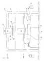
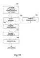
- FIG. 1is a schematic illustration of a lithography machine 10.
- the lithography machine 10includes a frame 12, an illumination system 14 (irradiation apparatus), an optical assembly 16, a reticle stage assembly 18, a work piece stage assembly 20, a measurement system 22, a control system 24, and a fluid environmental system 26.
- the design of the components of the lithography machine 10can be varied to suit the design requirements of the lithography machine 10.
- the lithography machine 10is used to transfer a pattern (not shown) of an integrated circuit from a reticle 28 onto a semiconductor wafer 30 (illustrated in phantom).
- the lithography machine 10mounts to a mounting base 32, e.g., the ground, a base, or floor or some other supporting structure.
- the lithography machine 10can be used as a scanning type photolithography system that exposes the pattern from the reticle 28 onto the wafer 30 with the reticle 28 and the wafer 30 moving synchronously.
- a scanning type lithographic machinethe reticle 28 is moved perpendicularly to an optical axis of the optical assembly 16 by the reticle stage assembly 18 and the wafer 30 is moved perpendicularly to the optical axis of the optical assembly 16 by the wafer stage assembly 20. Scanning of the reticle 28 and the wafer 30 occurs while the reticle 28 and the wafer 30 are moving synchronously.
- the lithography machine 10can be a step-and-repeat type photolithography system that exposes the reticle 28 while the reticle 28 and the wafer 30 are stationary.
- the wafer 30is in a constant position relative to the reticle 28 and the optical assembly 16 during the exposure of an individual field.
- the wafer 30is consecutively moved with the wafer stage assembly 20 perpendicularly to the optical axis of the optical assembly 16 so that the next field of the wafer 30 is brought into position relative to the optical assembly 16 and the reticle 28 for exposure.
- the images on the reticle 28are sequentially exposed onto the fields of the wafer 30, and then the next field of the wafer 30 is brought into position relative to the optical assembly 16 and the reticle 28.
- the use of the lithography machine 10 provided hereinis not necessarily limited to a photolithography for semiconductor manufacturing.
- the lithography machine 10for example, can be used as an LCD photolithography system that exposes a liquid crystal display work piece pattern onto a rectangular glass plate or a photolithography system for manufacturing a thin film magnetic head.
- the term "work piece”is generically used herein to refer to any device that may be patterned using lithography, such as but not limited to wafers or LCD substrates.
- the apparatus frame 12supports the components of the lithography machine 10.
- the apparatus frame 12 illustrated in Figure 1supports the reticle stage assembly 18, the wafer stage assembly 20, the optical assembly 16 and the illumination system 14 above the mounting base 32.
- the illumination system 14includes an illumination source 34 and an illumination optical assembly 36.
- the illumination source 34emits a beam (irradiation) of light energy.
- the illumination optical assembly 36guides the beam of light energy from the illumination source 34 to the optical assembly 16.
- the beamilluminates selectively different portions of the reticle 28 and exposes the wafer 30.
- the illumination source 34is illustrated as being supported above the reticle stage assembly 18. Typically, however, the illumination source 34 is secured to one of the sides of the apparatus frame 12 and the energy beam from the illumination source 34 is directed to above the reticle stage assembly 18 with the illumination optical assembly 36.
- the illumination source 34can be a g-line source (436 nm), an i-line source (365 nm), a KrF excimer laser (248 nm), an ArF excimer laser (193 nm) or a F 2 laser (157 nm). Alternatively, the illumination source 34 can generate charged an x-ray.
- the optical assembly 16projects and/or focuses the light passing through the reticle 28 to the wafer 30. Depending upon the design of the lithography machine 10, the optical assembly 16 can magnify or reduce the image illuminated on the reticle 28.
- the optical assembly 16need not be limited to a reduction system. It could also be a 1x or greater magnification system.
- the catadioptric type optical systemcan be considered.
- the catadioptric type of optical systeminclude the disclosure Japan Patent Application Disclosure No. 8-171054 published in the Official Gazette for Laid-Open Patent Applications and its counterpart U.S. Patent No, 5,668,672 , as well as Japan Patent Application Disclosure No. 10-20195 and its counterpart U.S. Patent No. 5,835,275 .
- the reflecting optical work piececan be a catadioptric optical system incorporating a beam splitter and concave mirror.
- the reticle stage assembly 18holds and positions the reticle 28 relative to the optical assembly 16 and the wafer 30.
- the reticle stage assembly 18includes a reticle stage 38 that retains the reticle 28 and a reticle stage mover assembly 40 that moves and positions the reticle stage 38 and reticle 28.
- Each stage mover assembly 40, 44can move the respective stage 38, 42 with three degrees of freedom, less than three degrees of freedom, or more than three degrees of freedom.
- each stage mover assembly 40, 44can move the respective stage. 38, 42 with one, two, three, four, five or six degrees of freedom.
- the reticle stage mover assembly 40 and the work piece stage mover assembly 44can each include one or more movers, such as rotary motors, voice coil motors, linear motors utilizing a Lorentz force to generate drive force, electromagnetic movers, planar motors, or some other force movers.
- the linear motorscan be either an air levitation type employing air bearings or a magnetic levitation type using Lorentz force or reactance force.
- the stagecould move along a guide, or it could be a guideless type stage that uses no guide.
- one of the stagescould be driven by a planar motor, which drives the stage by an electromagnetic force generated by a magnet unit having two-dimensionally arranged magnets and an armature coil unit having two-dimensionally arranged coils in facing positions.
- a planar motorwhich drives the stage by an electromagnetic force generated by a magnet unit having two-dimensionally arranged magnets and an armature coil unit having two-dimensionally arranged coils in facing positions.
- either the magnet unit or the armature coil unitis connected to the stage base and the other unit is mounted on the moving plane side of the stage.
- reaction forces generated by the wafer (substrate) stage motioncan be mechanically transferred to the floor (ground) by use of a frame member as described in US Patent No. 5,528,100 and published Japanese Patent Application Disclosure No. 8-136475 .
- reaction forces generated by the reticle (mask) stage motioncan be mechanically transferred to the floor (ground) by use of a frame member as described in US Patent No. 5,874,820 and published Japanese Patent Application Disclosure No. 8-330224 .
- the measurement system 22monitors movement of the reticle 28 and the wafer 30 relative to the optical assembly 16 or some other reference. With this information, the control system 24 can control the reticle stage assembly 18 to precisely position the reticle 28 and the work piece stage assembly 20 to precisely position the wafer 30.
- the design of the measurement system 22can vary. For example, the measurement system 22 can utilize multiple laser interferometers, encoders, mirrors, and/or other measuring devices.
- the control system 24receives information from the measurement system 22 and controls the stage mover assemblies 18, 20 to precisely position the reticle 28 and the wafer 30. Additionally, the control system 24 can control the operation of the components of the environmental system 26.
- the control system 24can include one or more processors and circuits.
- the environmental system 26controls the environment in a gap (not shown) between the optical assembly 16 and the wafer 30.
- the gapincludes an imaging field.
- the imaging fieldincludes the area adjacent to the region of the wafer 30 that is being exposed and the area in which the beam of light energy travels between the optical assembly 16 and the wafer 30.
- the environmental system 26can control the environment in the imaging field.
- the desired environment created and/or controlled in the gap by the environmental system 26can vary accordingly to the wafer 30 and the design of the rest of the components of the lithography machine 10, including the illumination system 14.
- the desired controlled environmentcan be a fluid such as water.
- the desired controlled environmentcan be another type of fluid such as a gas.
- the gapmay range from 0.1mm to 10mm in height between top surface of the wafer 30 and the last optical element of the optical assembly 16.
- the environmental system 26fills the imaging field and the rest of the gap with an immersion fluid.
- the design of the environmental system 26 and the components of the environmental system 26can be varied.
- the environmental system 26delivers and/or injects immersion fluid into the gap using spray nozzles, electro-kinetic sponges, porous materials, etc. and removes the fluid from the gap using vacuum pumps, sponges, and the like.
- the design of the environmental system 26can vary. For example, it can inject the immersion fluid at one or more locations at or near the gap. Further, the immersion fluid system can assist in removing and/or scavenging the immersion fluid at one or more locations at or near the work piece 30, the gap and/or the edge of the optical assembly 16.
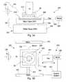
- the lithography machine 200includes a optical assembly 16 and a stage assembly 202 that includes a wafer table 204 and a wafer stage 206.
- the wafer table 204is configured to support a wafer 208 (or any other type of work piece) under the optical assembly 16.
- An environmental system 26, surrounding the optical assembly 16,is used to supply and remove immersion fluid 212 from the gap between the wafer 208 and the last optical element of the optical assembly 16.
- a work piece exchange system 216including a wafer loader 218 (i.e., a robot) and an alignment tool 220 (i.e., a microscope and CCD camera), is configured to remove the wafer 208 on the wafer table 204 and replace it with a second wafer. This is typically accomplished using the wafer loader 218 to lift and remove the wafer 208 from the wafer table 204. Subsequently, the second wafer (not shown) is placed onto the wafer chuck 218, aligned using the alignment tool 220, and then positioned under the optical assembly 16 on the wafer table 204.
- a wafer loader 218i.e., a robot
- an alignment tool 220i.e., a microscope and CCD camera
- the wafer stage 206includes an immersion fluid containment system 214 that is configured to maintain the immersion fluid 212 in the gap adjacent the last optical element of the optical assembly 16 during wafer exchange.
- the immersion fluid containment system 214includes a pad 222 that is adjacent the wafer table 204.
- a support member 224provided between the pad 222 and the wafer stage 206, is used to support the pad 222.
- the wafer table 204has a flat upper surface which is coplanar with a surface of the wafer 208.
- the pad 222also has a flat upper surface which is coplanar with the upper surface of the wafer table 204 and the wafer surface.
- the pad 222is arranged adjacent the wafer table 204 with a very small gap (e.g.
- the wafer stage 206is moved in the direction of arrow 226 so that the pad 222 is positioned under the optical assembly 16 in place of the wafer table 204, maintaining the fluid in the gap or maintaining the size of the fluid gap.
- the wafer stageis moved back to its original position so that the pad 222 is removed from the gap as the second wafer is positioned under the optical assembly 16.
- the pad 222is disposed continuously adjacent the wafer table 204 with no gap.
- Vertical position and/or tilt of the wafer table 204can be adjusted so that the wafer table surface is coplanar with the pad surface, before the wafer table 204 is moved out from under the optical assembly 16. Maintaining the gap between the pad 222 and the optical assembly 16 is not limited to just a wafer exchange operation.
- the pad 222can be large enough to maintain the immersion fluid 212 in the space between the pad 222 and the optical assembly 16 during an alignment operation or a measurement operation. In those operations, a part of the area occupied by the immersion fluid 212 may be on the upper surface of the wafer table 204.
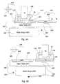
- the lithography machine 300includes an optical assembly 16 and a stage assembly 302 that includes a wafer table 304 and a wafer stage 306.
- the wafer table 304is configured to support a wafer 308 (or any other type of work piece) under the optical assembly 16.
- An environmental system 26, surrounding the optical assembly 16,is used to supply and remove immersion fluid 312 from the gap between the wafer 308 and the lower most optical element of the optical assembly 16.
- a work piece exchange system 316including a wafer loader 318 and an alignment tool 320, is configured to remove the wafer 308 on the wafer table 304 and replace it with a second wafer.
- a set of motors 322are used to move the wafer assembly 302 including the wafer table 304 and wafer stage 306 in two degrees of freedom (X and Y) during operation.
- the motors 322can be any type of motors, such as linear motors, rotary motors, voice coil motors, etc.
- the immersion lithography machine 300also includes an immersion fluid containment system 324 that is configured to maintain the immersion fluid 312 in the space below the optical assembly 16 while the wafer table 304 is away from under the optical assembly.
- The, immersion fluid containment system 324includes a pad 326, a motor 328, and a control system 330.
- the pad 326can be positioned adjacent the optical assembly 16 and the wafer table 204.
- the wafer table 304has a flat upper surface which is coplanar with a surface of the wafer 308.
- the pad 326has a flat upper surface which is coplanar with the upper surface of the wafer table 304 and the wafer surface.
- the pad 326is movable in the X and Y directions using the motor 328 which is controlled by the control system 330.
- the motor 328can be any type of motors as well as the motors 322.
- the pad 326is positioned under the optical assembly 16 when the wafer table 304 (the wafer stage 306) is away from under the optical assembly 16. During a wafer exchange, the wafer table 304 moves away from the optical assembly 16. Simultaneously, the control system 330 directs the motor 328 to move pad 326 under the optical assembly 16, replacing the wafer table 308. The pad 326 thus retains the immersion fluid 312 within the gap under the optical assembly 16. After the new wafer has been aligned using the alignment tool 320, the wafer table 304 is repositioned under the optical assembly 16.
- the control system 330directs the motor 328 to retract the pad 326 from the gap, preventing the escape of the immersion fluid 312.
- the control system 330moves the wafer table 304 and the pad 326 with a small gap between the wafer table 304 and the pad 326, while the immersion fluid 312 below the optical assembly 16 moves between the wafer table 304 and the pad 326.
- the immersion fluid containment system 324thus maintains the immersion fluid 312 from the gap during wafer exchange.
- the wafer table 304(the wafer stage 306) and the pad 326 are movable separately. Therefore, the wafer table 326 is movable freely while the immersion fluid 312 is maintained in the space between the pad 326 and the optical assembly 16.
- control system 330may be a separate control system or it can be integrated into the control system used to control the motors 322 for positioning the wafer stage 302 and wafer table 304.
- Vertical position and/or tilt of at least one of the wafer table 304 and the pad 326may be adjusted so that the wafer table surface is coplanar with the pad surface, before the wafer table is moved out from under the optical assembly 16.
- the operation, in which the wafer table 304 is away from the optical assembly 16,is not necessarily limited to a wafer exchange operation. For example, an alignment operation, a measurement operation or other operation may be executed while maintaining the immersion fluid 312 in the space between the pad 326 and the optical assembly 16.
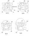
- the lithography machine 400includes an optical assembly 16 and a stage assembly 402 that includes a wafer table 404 and a wafer stage 406.
- the wafer table 404is configured to support a wafer 408 (or any other type of work piece) under the optical assembly 16.
- An environmental system 26, surrounding the optical assembly 16,is used to supply and remove immersion fluid 412 from the gap between the wafer 408 and the lower most optical element of the optical assembly 16.
- a work piece exchange system 416including a wafer loader 418 and an alignment tool 420, is configured to remove the wafer 408 on the wafer table 404 and replace it with a second wafer.
- the wafer loader 418to remove the wafer 408 from the wafer table 404.
- the second wafer(not shown) is placed onto the wafer chuck 418, aligned using the alignment tool 420, and then positioned under the optical assembly 16 as illustrated in the Figure 4A .
- the immersion lithography machine 400also includes an immersion fluid containment system 424 that is configured to maintain the immersion fluid 412 in the space below the optical assembly 16 while the wafer table 404 is away from under the optical assembly 16.
- the immersion fluid containment system 424includes a pad 426, a first clamp 428 provided on the optical assembly 16 and a second clamp 430 provided on the wafer table 404.
- the pad 426is held by the second clamp 430 in place on the wafer table 404.
- the pad 426When the wafer table 404 is away from the optical assembly 16, for example during a wafer exchange operation, the pad 426 is detached from the wafer table 404 and held by the first clamp 428 to maintain the immersion fluid 412 between the optical assembly 16 and the pad 426.
- the wafer table 404has a flat upper surface which is coplanar with a surface of the wafer 408.
- the pad 426 held on the wafer table 404also has a flat upper surface which is coplanar with the upper surface of the wafer table 404 and the wafer surface. Therefore, the immersion pad 426 and wafer 408 can be moved under the optical assembly without the immersion fluid leaking.
- the clamps 428 and 430can be vacuum clamps, magnetic, electro-static, or mechanical.
- the pad 426is positioned on the wafer table 404 during exposure of the wafer 408.
- the second clamp 430is used to hold the pad 426 in place on the table 404 during the wafer exposure.
- the wafer table 404is moved in the direction of arrow 432 so that the pad 426 is positioned under the optical assembly 16 in place of the wafer 408.
- the second clamp 430 holding the pad 426 to the wafer table 404is released while first clamp 428 clamps the pad 426 to the optical assembly 16.
- the immersion fluid 412is maintained under the optical assembly while the wafer 408 is exchanged.
- the wafer table 404is moved in the direction opposite arrow 432 so that the new wafer is positioned under the optical assembly. Prior to this motion, the first clamp 428 is released while the second clamp 430 again clamps the pad 426 to the wafer table 404. In this embodiment, the wafer table 404 is freely movable while the pad 426 is clamped by the first clamp 428.
- the operation, in which the pad 426 is clamped by the first clamp 428is not limited to only a wafer exchange operation.
- An alignment operation, a measurement operation, or any other operationcan be executed while the immersion fluid 312 is maintained in the space between the optical assembly 16 and the pad 426 clamped by the first clamp 428.
- the clamp 428can be provided on the frame 12 or other support member, and the clamp 430 can be provided on the wafer stage 406.
- the pad 426can be held on a movable member other than the stage assembly 402.
- FIGS. 5A and 5Bare top down views of two different twin stage immersion lithography systems of the present invention.
- a pair of wafer stages WS1 and WS2are shown.
- Motors 502are used to move or position the two stages WS1 and WS2 in the horizontal directions whereas motors 504 are used to move or position the stages WS1 and WS2 in the vertical direction.
- the motors 502 and 504are used to alternatively position one stage under the optical assembly 16 while a wafer exchange and alignment is performed on the other stage.
- each wafer stage SW1 and SW2 of either Figure 5A or 5Bcan be modified to include a pad 222 and a support member 224.
- a single pad 326, motor 328, and control system 330could be used adjacent the optical assembly 16. The pad 326 is movable separately from the stage SW1 and SW2.
- stage SW1 and SW2are to be swapped.
- the pad 326is moved to under the optical assembly 16 to maintain the immersion fluid 312 below the optical assembly 16.
- a detachable single padcan be used.
- the pad 426is used to maintain the immersion fluid in the gap as illustrated in Figure 4B .
- the padis clamped onto the wafer table on the wafer stage that is being exposed. In this manner, only a single pad is needed for the two stages WS1 and WS2.
- the second stagecan also be used as the pad.
- the immersion lithography system 600includes first stage 604 and second stage 606.
- the two stagesare moved in the X and Y directions by motors 602.
- the stages 604 and 606themselves are used to contain the immersion fluid in the gap.
- the first stage 604is positioned under the optical assembly 16.
- the motors 602are used to position the second stage 606 with a second work piece adjacent the first stage 604. With the two stages positioned side-by-side, they substantially form a continuous surface.
- the motors 602are then used to move the two stages in unison so that the second stage 604 is position under the optical assembly 16 and the first stage is no longer under the optical assembly 16.
- the immersion fluid in the gapis maintained by the second stage 606 which forms the substantially continuous surface with the first stage.
- the second stage 606could also be a "pad" stage that contains a pad that is used to maintain the immersion liquid in the gap while a second work piece is being placed onto the first stage 604.
- the motor arrangement shown in either Figure 5A or 5Bcould be used.
- Figure 6B-6Ea series of diagrams illustrating a work piece exchange is illustrated.
- Figure 6Bshows a wafer on stage 604 after exposure is completed.
- Figure 6Cshows the second stage 606 in contact (or immediately adjacent) with the first stage 604 under the optical assembly 16.
- Figure 6Cshows a transfer taking place, i.e., the second stage 606 is positioned under the optical assembly 16.
- the first stage 604is moved away from the optical assembly 16.
- the two stages 604 and 606provide a continuous surface under the optical assembly 16 during a transfer, thus maintaining the immersion fluid in the gap.
- the second stage 606is a pad stage. This stage, however, could also be a work piece stage as noted above.
- the padcan be made of a number of different materials, such as ceramic, metal plastic. These materials may also be coated with Teflon according to other embodiments.
- the size of the padalso should be sufficient to cover the area occupied by the immersion fluid.
- the surface of the last optical element, of the optical assembly 16is constantly under immersion fluid environment, preventing the formation of a fluid mark (e.g. "a water mark").
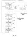
- step 701the work piece's function and performance characteristics are designed.
- step 702a mask (reticle) having a pattern is designed according to the previous designing step, and in a parallel step 703 a wafer is made from a silicon material.
- the mask pattern designed in step 702is exposed onto the wafer from step 703 in step 704 by a photolithography system described hereinabove in accordance with the present invention.
- step 705the semiconductor work piece is assembled (including the dicing process, bonding process and packaging process), finally, the work piece is then inspected in step 606.
- FIG. 7Billustrates a detailed flowchart example of the above-mentioned step 704 in the case of fabricating semiconductor work pieces.
- step 711oxidation step
- step 712CVD step
- step 713electrode formation step
- step 714ion implantation step
- steps 711 - 714form the preprocessing steps for wafers during wafer processing, and selection is made at each step according to processing requirements.
- step 715photoresist formation step
- step 716exposure step
- step 717developing step
- step 718etching step
- steps other than residual photoresistexposed material surface
- circuit patternsare formed by repetition of these preprocessing and post-processing steps.
Landscapes
- Physics & Mathematics (AREA)
- General Physics & Mathematics (AREA)
- Engineering & Computer Science (AREA)
- Condensed Matter Physics & Semiconductors (AREA)
- Manufacturing & Machinery (AREA)
- Computer Hardware Design (AREA)
- Microelectronics & Electronic Packaging (AREA)
- Power Engineering (AREA)
- Health & Medical Sciences (AREA)
- Optics & Photonics (AREA)
- Environmental & Geological Engineering (AREA)
- Epidemiology (AREA)
- Public Health (AREA)
- Toxicology (AREA)
- Exposure And Positioning Against Photoresist Photosensitive Materials (AREA)
- Exposure Of Semiconductors, Excluding Electron Or Ion Beam Exposure (AREA)
- Container, Conveyance, Adherence, Positioning, Of Wafer (AREA)
Description
- This application claims priority on Provisional Application Serial No.
60/462,499 filed on April 11, 2003 - Lithography systems are commonly used to transfer images from a reticle onto a semiconductor wafer during semiconductor processing. A typical lithography system includes an optical assembly, a reticle stage for holding a reticle defining a pattern, a wafer stage assembly that positions a semiconductor wafer, and a measurement system that precisely monitors the position of the reticle and the wafer. During operation, an image defined by the reticle is projected by the optical assembly onto the wafer. The projected image is typically the size of one or more die on the wafer. After an exposure, the wafer stage assembly moves the wafer and another exposure takes place. This process is repeated until all the dice on the wafer are exposed. The wafer is then removed and a new wafer is exchanged in its place.
- Immersion lithography systems utilize a layer of immersion fluid that completely fills a gap between the optical assembly and the wafer during the exposure of the wafer. The optic properties of the immersion fluid, along with the optical assembly, allow the projection of smaller feature sizes than is currently possible using standard optical lithography. For example, immersion lithography is currently being considered for next generation semiconductor technologies including 65 nanometers, 45 nanometers, and beyond. Immersion lithography therefore represents a significant technological breakthrough that will likely enable the continued use of optical lithography for the foreseeable future.
- After a wafer is exposed, it is removed and exchanged with a new wafer. As currently contemplated in immersion systems, the immersion fluid would be removed from the gap and then replenished after the wafer is exchanged. Morse specifically, when a wafer is to be exchanged, the fluid supply to the gap is turned off, the fluid is removed from the gap (i.e., by vacuum), the old wafer is removed, a new wafer is aligned and placed under the optical assembly, and then the gap is re-filied with fresh immersion fluid. Once all of the above steps are complete, exposure of the new wafer can begin.
- Wafer exchange with immersion lithography as described above is problematic for a number of reasons. The repeated filling and draining of the gap may cause variations in the immersion fluid and may cause bubbles to form within the immersion fluid. Bubbles and the unsteady fluid may interfere with the projection of the image on the reticle onto the wafer, thereby reducing yields. The overall process also involves many steps and is time consuming, which reduces the overall throughput of the machine.
- An apparatus and method for maintaining immersion fluid in the gap adjacent the projection lens when the wafer stage moves away from the projection lens, for example during wafer exchange, is therefore needed.
- According to a first aspect of the present invention, there is provided an immersion exposure apparatus as recited in Claim 1 below.
- According to a second aspect of the present invention, there is provided a device manufacturing method as recited in
Claim 16 below. - According to a third aspect of the present invention, there is provided an immersion exposure method as recited in Claim 17 below.
- According to a fourth aspect of the present invention, there is provided a device manufacturing method as recited in
Claim 32 below. - Dependent claims define particular embodiments of the present invention.
Figure 1 is an illustration of an lithography machine having features of the present invention;Figure 2 is a cross section of an immersion lithography machine according to one embodiment of the present invention;Figures 3A and 3B are a cross section and a top down view of an immersion lithography machine according to another embodiment of the present invention;Figures 4A and 4B are a cross section and a top down view of an immersion lithography machine according to another embodiment of the present invention;Figures 5A and 5B are top down views of two different twin wafer stages according to other embodiments of the present invention;Figure 6A is a top down view of a twin stage lithography machine according to another embodiment of the invention;Figures 6B-6E are a series of diagrams illustrating a wafer exchange according to the present invention;Figure 7A is a flow chart that outlines a process for manufacturing a work piece in accordance with the present invention; andFigure 7B is a flow chart that outlines work piece processing in more detail.- Like reference numbers refer to like elements in the drawings.
- An apparatus and method for maintaining immersion fluid in the gap adjacent the projection lens in a lithography machine is disclosed. The apparatus and method includes an optical assembly configured to project an image onto a work piece and a stage assembly including a work piece table configured to support the work piece adjacent the optical assembly. An environmental system is provided to supply and remove an immersion fluid from the gap. After exposure of the work piece is complete, an exchange system removes the work piece and replaces it with a second work piece. An immersion fluid system is provided to maintain the immersion fluid in the gap when the work piece table moves away from the projection lens. The gap therefore does not have to be refilled with immersion fluid when the first work piece is replaced with a second work piece.
Figure 1 is a schematic illustration of alithography machine 10. Thelithography machine 10 includes aframe 12, an illumination system 14 (irradiation apparatus), anoptical assembly 16, areticle stage assembly 18, a workpiece stage assembly 20, ameasurement system 22, acontrol system 24, and a fluidenvironmental system 26. The design of the components of thelithography machine 10 can be varied to suit the design requirements of thelithography machine 10.- In one application, the
lithography machine 10 is used to transfer a pattern (not shown) of an integrated circuit from areticle 28 onto a semiconductor wafer 30 (illustrated in phantom). Thelithography machine 10 mounts to amounting base 32, e.g., the ground, a base, or floor or some other supporting structure. - In various configurations, the
lithography machine 10 can be used as a scanning type photolithography system that exposes the pattern from thereticle 28 onto thewafer 30 with thereticle 28 and thewafer 30 moving synchronously. In a scanning type lithographic machine, thereticle 28 is moved perpendicularly to an optical axis of theoptical assembly 16 by thereticle stage assembly 18 and thewafer 30 is moved perpendicularly to the optical axis of theoptical assembly 16 by thewafer stage assembly 20. Scanning of thereticle 28 and thewafer 30 occurs while thereticle 28 and thewafer 30 are moving synchronously. - Alternatively, the
lithography machine 10 can be a step-and-repeat type photolithography system that exposes thereticle 28 while thereticle 28 and thewafer 30 are stationary. In the step and repeat process, thewafer 30 is in a constant position relative to thereticle 28 and theoptical assembly 16 during the exposure of an individual field. Subsequently, between consecutive exposure steps, thewafer 30 is consecutively moved with thewafer stage assembly 20 perpendicularly to the optical axis of theoptical assembly 16 so that the next field of thewafer 30 is brought into position relative to theoptical assembly 16 and thereticle 28 for exposure. Following this process, the images on thereticle 28 are sequentially exposed onto the fields of thewafer 30, and then the next field of thewafer 30 is brought into position relative to theoptical assembly 16 and thereticle 28. - However, the use of the
lithography machine 10 provided herein is not necessarily limited to a photolithography for semiconductor manufacturing. Thelithography machine 10, for example, can be used as an LCD photolithography system that exposes a liquid crystal display work piece pattern onto a rectangular glass plate or a photolithography system for manufacturing a thin film magnetic head. Accordingly, the term "work piece" is generically used herein to refer to any device that may be patterned using lithography, such as but not limited to wafers or LCD substrates. - The
apparatus frame 12 supports the components of thelithography machine 10. Theapparatus frame 12 illustrated inFigure 1 supports thereticle stage assembly 18, thewafer stage assembly 20, theoptical assembly 16 and theillumination system 14 above themounting base 32. - The
illumination system 14 includes anillumination source 34 and an illuminationoptical assembly 36. Theillumination source 34 emits a beam (irradiation) of light energy. The illuminationoptical assembly 36 guides the beam of light energy from theillumination source 34 to theoptical assembly 16. The beam illuminates selectively different portions of thereticle 28 and exposes thewafer 30. InFigure 1 , theillumination source 34 is illustrated as being supported above thereticle stage assembly 18. Typically, however, theillumination source 34 is secured to one of the sides of theapparatus frame 12 and the energy beam from theillumination source 34 is directed to above thereticle stage assembly 18 with the illuminationoptical assembly 36. - The
illumination source 34 can be a g-line source (436 nm), an i-line source (365 nm), a KrF excimer laser (248 nm), an ArF excimer laser (193 nm) or a F2 laser (157 nm). Alternatively, theillumination source 34 can generate charged an x-ray. - The
optical assembly 16 projects and/or focuses the light passing through thereticle 28 to thewafer 30. Depending upon the design of thelithography machine 10, theoptical assembly 16 can magnify or reduce the image illuminated on thereticle 28. Theoptical assembly 16 need not be limited to a reduction system. It could also be a 1x or greater magnification system. - Also, with an exposure work piece that employs vacuum ultra-violet radiation (VUV) of
wavelength 200 nm or lower, use of the catadioptric type optical system can be considered. Examples of the catadioptric type of optical system include the disclosure Japan Patent Application Disclosure No.8-171054 U.S. Patent No, 5,668,672 , as well as Japan Patent Application Disclosure No.10-20195 U.S. Patent No. 5,835,275 . In these cases, the reflecting optical work piece can be a catadioptric optical system incorporating a beam splitter and concave mirror. Japan Patent Application Disclosure NO.8-334695 U.S. Patent No. 5,689,377 as well as Japan Patent Application Disclosure No.10-3039 U.S. Patent Application No. 873,605 (Application Date: 6-12-97) also use a reflecting-refracting type of optical system incorporating a concave mirror, etc., but without a beam splitter, and can also be employed with this invention. - The
reticle stage assembly 18 holds and positions thereticle 28 relative to theoptical assembly 16 and thewafer 30. In one embodiment, thereticle stage assembly 18 includes areticle stage 38 that retains thereticle 28 and a reticlestage mover assembly 40 that moves and positions thereticle stage 38 andreticle 28. - Each
stage mover assembly respective stage stage mover assembly stage mover assembly 40 and the work piecestage mover assembly 44 can each include one or more movers, such as rotary motors, voice coil motors, linear motors utilizing a Lorentz force to generate drive force, electromagnetic movers, planar motors, or some other force movers. - In photolithography systems, when linear motors (see
US Patent Numbers 5,623,853 or5,528,118 ) are used in the wafer stage assembly or the reticle stage assembly, the linear motors can be either an air levitation type employing air bearings or a magnetic levitation type using Lorentz force or reactance force. Additionally, the stage could move along a guide, or it could be a guideless type stage that uses no guide. - Alternatively, one of the stages could be driven by a planar motor, which drives the stage by an electromagnetic force generated by a magnet unit having two-dimensionally arranged magnets and an armature coil unit having two-dimensionally arranged coils in facing positions. With this type of driving system, either the magnet unit or the armature coil unit is connected to the stage base and the other unit is mounted on the moving plane side of the stage.
- Movement of the stages as described above generates reaction forces that can affect performance of the photolithography system. Reaction forces generated by the wafer (substrate) stage motion can be mechanically transferred to the floor (ground) by use of a frame member as described in
US Patent No. 5,528,100 and published Japanese Patent Application Disclosure No.8-136475 US Patent No. 5,874,820 and published Japanese Patent Application Disclosure No.8-330224 - The
measurement system 22 monitors movement of thereticle 28 and thewafer 30 relative to theoptical assembly 16 or some other reference. With this information, thecontrol system 24 can control thereticle stage assembly 18 to precisely position thereticle 28 and the workpiece stage assembly 20 to precisely position thewafer 30. The design of themeasurement system 22 can vary. For example, themeasurement system 22 can utilize multiple laser interferometers, encoders, mirrors, and/or other measuring devices. - The
control system 24 receives information from themeasurement system 22 and controls thestage mover assemblies reticle 28 and thewafer 30. Additionally, thecontrol system 24 can control the operation of the components of theenvironmental system 26. Thecontrol system 24 can include one or more processors and circuits. - The
environmental system 26 controls the environment in a gap (not shown) between theoptical assembly 16 and thewafer 30. The gap includes an imaging field. The imaging field includes the area adjacent to the region of thewafer 30 that is being exposed and the area in which the beam of light energy travels between theoptical assembly 16 and thewafer 30. With this design, theenvironmental system 26 can control the environment in the imaging field. The desired environment created and/or controlled in the gap by theenvironmental system 26 can vary accordingly to thewafer 30 and the design of the rest of the components of thelithography machine 10, including theillumination system 14. For example, the desired controlled environment can be a fluid such as water. Alternatively, the desired controlled environment can be another type of fluid such as a gas. In various embodiments, the gap may range from 0.1mm to 10mm in height between top surface of thewafer 30 and the last optical element of theoptical assembly 16. - In one configuration, the
environmental system 26 fills the imaging field and the rest of the gap with an immersion fluid. The design of theenvironmental system 26 and the components of theenvironmental system 26 can be varied. In different embodiments, theenvironmental system 26 delivers and/or injects immersion fluid into the gap using spray nozzles, electro-kinetic sponges, porous materials, etc. and removes the fluid from the gap using vacuum pumps, sponges, and the like. The design of theenvironmental system 26 can vary. For example, it can inject the immersion fluid at one or more locations at or near the gap. Further, the immersion fluid system can assist in removing and/or scavenging the immersion fluid at one or more locations at or near thework piece 30, the gap and/or the edge of theoptical assembly 16. For additional details on various environmental systems, see ProvisionalUS applications 60/462,142 60/462,112 60/500,312 60/541,329 - Referring to
Figure 2 , a cross section of a lithography machine is shown. Thelithography machine 200 includes aoptical assembly 16 and astage assembly 202 that includes a wafer table 204 and awafer stage 206. The wafer table 204 is configured to support a wafer 208 (or any other type of work piece) under theoptical assembly 16. Anenvironmental system 26, surrounding theoptical assembly 16, is used to supply and removeimmersion fluid 212 from the gap between thewafer 208 and the last optical element of theoptical assembly 16. A workpiece exchange system 216, including a wafer loader 218 (i.e., a robot) and an alignment tool 220 (i.e., a microscope and CCD camera), is configured to remove thewafer 208 on the wafer table 204 and replace it with a second wafer. This is typically accomplished using thewafer loader 218 to lift and remove thewafer 208 from the wafer table 204. Subsequently, the second wafer (not shown) is placed onto thewafer chuck 218, aligned using thealignment tool 220, and then positioned under theoptical assembly 16 on the wafer table 204. - With this configuration, the
wafer stage 206 includes an immersionfluid containment system 214 that is configured to maintain theimmersion fluid 212 in the gap adjacent the last optical element of theoptical assembly 16 during wafer exchange. The immersionfluid containment system 214 includes apad 222 that is adjacent the wafer table 204. Asupport member 224, provided between thepad 222 and thewafer stage 206, is used to support thepad 222. The wafer table 204 has a flat upper surface which is coplanar with a surface of thewafer 208. Thepad 222 also has a flat upper surface which is coplanar with the upper surface of the wafer table 204 and the wafer surface. Thepad 222 is arranged adjacent the wafer table 204 with a very small gap (e.g. 0.1-1.0mm) so that theimmersion fluid 212 is movable between the wafer table 204 and thepad 222 without leaking. During a wafer exchange, thewafer stage 206 is moved in the direction ofarrow 226 so that thepad 222 is positioned under theoptical assembly 16 in place of the wafer table 204, maintaining the fluid in the gap or maintaining the size of the fluid gap. After the new wafer has been aligned, the wafer stage is moved back to its original position so that thepad 222 is removed from the gap as the second wafer is positioned under theoptical assembly 16. In various embodiments, thepad 222 is disposed continuously adjacent the wafer table 204 with no gap. Vertical position and/or tilt of the wafer table 204 can be adjusted so that the wafer table surface is coplanar with the pad surface, before the wafer table 204 is moved out from under theoptical assembly 16.
Maintaining the gap between thepad 222 and theoptical assembly 16 is not limited to just a wafer exchange operation. Thepad 222 can be large enough to maintain theimmersion fluid 212 in the space between thepad 222 and theoptical assembly 16 during an alignment operation or a measurement operation. In those operations, a part of the area occupied by theimmersion fluid 212 may be on the upper surface of the wafer table 204. - Referring to
Figure 3A and 3B , a cross section and a top down view of another immersion lithography machine is shown. Thelithography machine 300 includes anoptical assembly 16 and astage assembly 302 that includes a wafer table 304 and awafer stage 306. The wafer table 304 is configured to support a wafer 308 (or any other type of work piece) under theoptical assembly 16. Anenvironmental system 26, surrounding theoptical assembly 16, is used to supply and removeimmersion fluid 312 from the gap between thewafer 308 and the lower most optical element of theoptical assembly 16. A workpiece exchange system 316, including awafer loader 318 and analignment tool 320, is configured to remove thewafer 308 on the wafer table 304 and replace it with a second wafer. This is accomplished using thewafer loader 318 to remove thewafer 308 from the wafer table. Subsequently, the second wafer (not shown) is placed onto thewafer chuck 318, aligned using thealignment tool 320, and then positioned under theoptical assembly 16. As best illustrated inFigure 3B , a set ofmotors 322 are used to move thewafer assembly 302 including the wafer table 304 andwafer stage 306 in two degrees of freedom (X and Y) during operation. As noted above, themotors 322 can be any type of motors, such as linear motors, rotary motors, voice coil motors, etc. - The
immersion lithography machine 300 also includes an immersionfluid containment system 324 that is configured to maintain theimmersion fluid 312 in the space below theoptical assembly 16 while the wafer table 304 is away from under the optical assembly. The, immersionfluid containment system 324 includes apad 326, amotor 328, and acontrol system 330. Thepad 326 can be positioned adjacent theoptical assembly 16 and the wafer table 204. The wafer table 304 has a flat upper surface which is coplanar with a surface of thewafer 308. Thepad 326 has a flat upper surface which is coplanar with the upper surface of the wafer table 304 and the wafer surface. Thepad 326 is movable in the X and Y directions using themotor 328 which is controlled by thecontrol system 330. Themotor 328 can be any type of motors as well as themotors 322. Thepad 326 is positioned under theoptical assembly 16 when the wafer table 304 (the wafer stage 306) is away from under theoptical assembly 16. During a wafer exchange, the wafer table 304 moves away from theoptical assembly 16. Simultaneously, thecontrol system 330 directs themotor 328 to movepad 326 under theoptical assembly 16, replacing the wafer table 308. Thepad 326 thus retains theimmersion fluid 312 within the gap under theoptical assembly 16. After the new wafer has been aligned using thealignment tool 320, the wafer table 304 is repositioned under theoptical assembly 16. At the same time, thecontrol system 330 directs themotor 328 to retract thepad 326 from the gap, preventing the escape of theimmersion fluid 312. In the wafer exchange operation, thecontrol system 330 moves the wafer table 304 and thepad 326 with a small gap between the wafer table 304 and thepad 326, while theimmersion fluid 312 below theoptical assembly 16 moves between the wafer table 304 and thepad 326. The immersionfluid containment system 324 thus maintains theimmersion fluid 312 from the gap during wafer exchange. In this configuration, the wafer table 304 (the wafer stage 306) and thepad 326 are movable separately. Therefore, the wafer table 326 is movable freely while theimmersion fluid 312 is maintained in the space between thepad 326 and theoptical assembly 16. In various configurations, thecontrol system 330 may be a separate control system or it can be integrated into the control system used to control themotors 322 for positioning thewafer stage 302 and wafer table 304. Vertical position and/or tilt of at least one of the wafer table 304 and thepad 326 may be adjusted so that the wafer table surface is coplanar with the pad surface, before the wafer table is moved out from under theoptical assembly 16. The operation, in which the wafer table 304 is away from theoptical assembly 16, is not necessarily limited to a wafer exchange operation. For example, an alignment operation, a measurement operation or other operation may be executed while maintaining theimmersion fluid 312 in the space between thepad 326 and theoptical assembly 16. - Referring to
Figure 4A and 4B , two cross sections of an immersion lithography machine which is an embodiment of the present invention are shown. Thelithography machine 400 includes anoptical assembly 16 and astage assembly 402 that includes a wafer table 404 and awafer stage 406. The wafer table 404 is configured to support a wafer 408 (or any other type of work piece) under theoptical assembly 16. Anenvironmental system 26, surrounding theoptical assembly 16, is used to supply and removeimmersion fluid 412 from the gap between thewafer 408 and the lower most optical element of theoptical assembly 16. A workpiece exchange system 416, including awafer loader 418 and analignment tool 420, is configured to remove thewafer 408 on the wafer table 404 and replace it with a second wafer. This is accomplished using thewafer loader 418 to remove thewafer 408 from the wafer table 404. Subsequently, the second wafer (not shown) is placed onto thewafer chuck 418, aligned using thealignment tool 420, and then positioned under theoptical assembly 16 as illustrated in theFigure 4A . - The
immersion lithography machine 400 also includes an immersionfluid containment system 424 that is configured to maintain theimmersion fluid 412 in the space below theoptical assembly 16 while the wafer table 404 is away from under theoptical assembly 16. The immersionfluid containment system 424 includes apad 426, afirst clamp 428 provided on theoptical assembly 16 and asecond clamp 430 provided on the wafer table 404. When theimmersion fluid 412 is between theoptical assembly 16 and the wafer table 404 (or the wafer 408), thepad 426 is held by thesecond clamp 430 in place on the wafer table 404. When the wafer table 404 is away from theoptical assembly 16, for example during a wafer exchange operation, thepad 426 is detached from the wafer table 404 and held by thefirst clamp 428 to maintain theimmersion fluid 412 between theoptical assembly 16 and thepad 426. The wafer table 404 has a flat upper surface which is coplanar with a surface of thewafer 408. Thepad 426 held on the wafer table 404 also has a flat upper surface which is coplanar with the upper surface of the wafer table 404 and the wafer surface. Therefore, theimmersion pad 426 andwafer 408 can be moved under the optical assembly without the immersion fluid leaking. In various embodiments, theclamps - As best illustrated in
Figure 4A , thepad 426 is positioned on the wafer table 404 during exposure of thewafer 408. Thesecond clamp 430 is used to hold thepad 426 in place on the table 404 during the wafer exposure. During a wafer exchange as illustrated inFigure 4B , the wafer table 404 is moved in the direction ofarrow 432 so that thepad 426 is positioned under theoptical assembly 16 in place of thewafer 408. When this occurs, thesecond clamp 430 holding thepad 426 to the wafer table 404 is released whilefirst clamp 428 clamps thepad 426 to theoptical assembly 16. As a result, theimmersion fluid 412 is maintained under the optical assembly while thewafer 408 is exchanged. After the new wafer has been aligned, the wafer table 404 is moved in the direction oppositearrow 432 so that the new wafer is positioned under the optical assembly. Prior to this motion, thefirst clamp 428 is released while thesecond clamp 430 again clamps thepad 426 to the wafer table 404. In this embodiment, the wafer table 404 is freely movable while thepad 426 is clamped by thefirst clamp 428. - In various embodiments, the operation, in which the
pad 426 is clamped by thefirst clamp 428, is not limited to only a wafer exchange operation. An alignment operation, a measurement operation, or any other operation can be executed while theimmersion fluid 312 is maintained in the space between theoptical assembly 16 and thepad 426 clamped by thefirst clamp 428. Also, theclamp 428 can be provided on theframe 12 or other support member, and theclamp 430 can be provided on thewafer stage 406. Thepad 426 can be held on a movable member other than thestage assembly 402. Figure 5A and 5B are top down views of two different twin stage immersion lithography systems of the present invention. For the basic structure and operation of the twin stage lithography systems, seeUS Patent No. 6,262,796 andUS Patent No. 6,341,007 . In both configurations, a pair of wafer stages WS1 and WS2 are shown.Motors 502 are used to move or position the two stages WS1 and WS2 in the horizontal directions whereasmotors 504 are used to move or position the stages WS1 and WS2 in the vertical direction. Themotors optical assembly 16 while a wafer exchange and alignment is performed on the other stage. When the exposure of the wafer under theoptical assembly 16 is complete, then the two stages are swapped and the above process is repeated. With either configuration, the various configurations for maintaining immersion fluid in the gap under theoptical assembly 16 as described and illustrated above with regard toFigures 2 through 4 , can be used with either twin stage arrangement. With regard to the configuration ofFigure 2 for example, each wafer stage SW1 and SW2 of eitherFigure 5A or 5B can be modified to include apad 222 and asupport member 224. With regard to the configuration ofFigure 3 , asingle pad 326,motor 328, andcontrol system 330 could be used adjacent theoptical assembly 16. Thepad 326 is movable separately from the stage SW1 and SW2. During the time when stage SW1 and SW2 are to be swapped, thepad 326 is moved to under theoptical assembly 16 to maintain theimmersion fluid 312 below theoptical assembly 16. Finally with the embodiment ofFigure 4 , a detachable single pad can be used. During the time when stage SW1 and SW2 are to be swapped, thepad 426 is used to maintain the immersion fluid in the gap as illustrated inFigure 4B . On the other hand during exposure, the pad is clamped onto the wafer table on the wafer stage that is being exposed. In this manner, only a single pad is needed for the two stages WS1 and WS2. Alternatively, as described below, the second stage can also be used as the pad.- Referring to
Figure 6A , a top down view of a twin stage lithography machine is shown. In this configuration, theimmersion lithography system 600 includesfirst stage 604 andsecond stage 606. The two stages are moved in the X and Y directions bymotors 602. In this embodiment, thestages first stage 604 is positioned under theoptical assembly 16. When it is time for the work piece to be exchanged, themotors 602 are used to position thesecond stage 606 with a second work piece adjacent thefirst stage 604. With the two stages positioned side-by-side, they substantially form a continuous surface. Themotors 602 are then used to move the two stages in unison so that thesecond stage 604 is position under theoptical assembly 16 and the first stage is no longer under theoptical assembly 16. Thus when the first work piece is moved away from theoptical assembly 16, the immersion fluid in the gap is maintained by thesecond stage 606 which forms the substantially continuous surface with the first stage. In various alternative configurations, thesecond stage 606 could also be a "pad" stage that contains a pad that is used to maintain the immersion liquid in the gap while a second work piece is being placed onto thefirst stage 604. Similarly, the motor arrangement shown in eitherFigure 5A or 5B could be used. - Referring to
Figures 6B-6E , a series of diagrams illustrating a work piece exchange is illustrated.Figure 6B shows a wafer onstage 604 after exposure is completed.Figure 6C shows thesecond stage 606 in contact (or immediately adjacent) with thefirst stage 604 under theoptical assembly 16.Figure 6C shows a transfer taking place, i.e., thesecond stage 606 is positioned under theoptical assembly 16. Finally, inFigure 6E , thefirst stage 604 is moved away from theoptical assembly 16. As best illustrated inFigures 6C and 6D , the twostages optical assembly 16 during a transfer, thus maintaining the immersion fluid in the gap. In the configuration shown, thesecond stage 606 is a pad stage. This stage, however, could also be a work piece stage as noted above. - In the various embodiments and related configurations described above, the pad can be made of a number of different materials, such as ceramic, metal plastic. These materials may also be coated with Teflon according to other embodiments. The size of the pad also should be sufficient to cover the area occupied by the immersion fluid. In the various embodiments described above, the surface of the last optical element, of the
optical assembly 16 is constantly under immersion fluid environment, preventing the formation of a fluid mark (e.g. "a water mark"). - Semiconductor wafers can be fabricated using the above described systems, by the process shown generally in
Figure 7A . Instep 701 the work piece's function and performance characteristics are designed. Next, instep 702, a mask (reticle) having a pattern is designed according to the previous designing step, and in a parallel step 703 a wafer is made from a silicon material. The mask pattern designed instep 702 is exposed onto the wafer fromstep 703 instep 704 by a photolithography system described hereinabove in accordance with the present invention. Instep 705 the semiconductor work piece is assembled (including the dicing process, bonding process and packaging process), finally, the work piece is then inspected instep 606. Figure 7B illustrates a detailed flowchart example of the above-mentionedstep 704 in the case of fabricating semiconductor work pieces. InFigure 7B , in step 711 (oxidation step), the wafer surface is oxidized. In step 712 (CVD step), an insulation film is formed on the wafer surface. In step 713 (electrode formation step), electrodes are formed on the wafer by vapor deposition. In step 714 (ion implantation step), ions are implanted in the wafer. The above mentioned steps 711 - 714 form the preprocessing steps for wafers during wafer processing, and selection is made at each step according to processing requirements.- At each stage of wafer processing, when the above-mentioned preprocessing steps have been completed, the following post-processing steps are implemented. During post-processing, first, in step 715 (photoresist formation step), photoresist is applied to a wafer. Next, in step 716 (exposure step), the above-mentioned exposure work piece is used to transfer the circuit pattern of a mask (reticle) to a wafer. Then in step 717 (developing step), the exposed wafer is developed, and in step 718 (etching step), parts other than residual photoresist (exposed material surface) are removed by etching. In step 719 (photoresist removal step), unnecessary photoresist remaining after etching is removed.
- Multiple circuit patterns are formed by repetition of these preprocessing and post-processing steps.
- While the particular lithography machines as shown and disclosed herein is fully capable of obtaining the objects and providing the advantages herein before stated, it is to be understood that it is merely illustrative of the presently preferred embodiments of the invention and that no limitations are intended to the details of construction or design herein shown other than as described in the appended claims.
The following numbered paragraphs set out particular combinations of features which are considered relevant to the present disclosure. - 1. An apparatus, comprising:
- an optical assembly configured to project an image onto a work piece;
- a stage assembly including a work piece table configured to support the work piece adjacent the optical assembly; and
- an immersion fluid system configured to substantially maintain an immersion fluid in a gap adjacent the optical assembly when the work piece table is moved away from the optical assembly.
- 2. The apparatus of paragraph 1, wherein the immersion fluid containment system comprises:
- a pad positioned adjacent the work piece; and
- a stage assembly mover configured to move the stage assembly such that the pad is positioned adjacent the optical assembly to maintain the immersion fluid in the gap.
- 3. The apparatus of paragraph 2, wherein the immersion fluid system further comprises a first clamp configured to hold the pad adjacent the optical assembly to maintain the immersion fluid in the gap.
- 4. The apparatus of paragraph 3, wherein the first clamp is mechanically coupled to a housing attached to the optical assembly.
- 5. The apparatus of paragraph 3, further comprising a second clamp on the stage assembly, the second clamp configured to hold the pad onto the work piece table when the work piece table is adjacent the optical assembly.
- 6. The apparatus of paragraph 3, further comprising a second clamp on the stage assembly, the second clamp configured to hold the pad onto the stage assembly when the work piece table is adjacent the optical assembly.
- 7. The apparatus of paragraph 5, wherein the first clamp is configured to clamp the pad when the work piece table is being moved away from the optical assembly and to release the pad when the work piece table is adjacent the optical assembly.
- 8. The apparatus of paragraph 6, wherein the second clamp is configured to clamp the pad when the work piece table is being moved away from the optical assembly and to release the pad when the work piece table is adjacent the optical assembly.
- 9. The apparatus of paragraph 3, wherein the clamp comprises one of the following types of clamps: vacuum, magnetic, electro-static, or mechanical.
- 10. The apparatus of paragraph 1, wherein the immersion fluid system further comprises:
- a pad positioned adjacent the optical assembly and stage assembly including the work piece table; and
- a motor, coupled to the pad, and configured to insert the pad into the gap to maintain the immersion fluid in the gap when the work piece table is moved away from the optical assembly.
- 11. The apparatus of paragraph 1, wherein the stage assembly further comprises a work piece stage positioned adjacent the work piece table and configured to move the work piece table, the work piece stage further including a pad that is configured to be inserted into the gap to maintain the immersion fluid in the gap when the work piece exchange system is exchanging the work piece.
- 12. The apparatus of paragraph 9, wherein the work piece stage further comprises a support member configured to support the pad adjacent the gap when the work piece exchange system is not exchanging the work piece and to position the pad in the gap when the work piece exchange system is exchanging the work piece.
- 13. The apparatus of paragraph 1, further comprising:
- a second stage assembly including a second work piece table configured to support a second work piece; and
- a control system configured to control the movement of the first stage assembly and the second stage assembly such that the two stage assemblies are alternatively positioned under the optical assembly.
- 14. The apparatus of paragraph 1, further comprising a work piece exchange system configured to remove the work piece on the work piece table and to replace it with a second work piece.
- 15. The apparatus of
paragraph 14, wherein the work piece exchange system comprises a robot to remove the work piece and to replace it with the second work piece. - 16. The apparatus of paragraph 1, further comprising an alignment tool to align the work piece.
- 17. The apparatus of paragraph 1, further comprising an environmental system configured to supply and remove immersion fluid into and from the gap.
- 18. The apparatus of paragraph 1, wherein the stage assembly includes the work piece table and a second work piece table, the work piece table and the second work piece table being configured to alternatively support the work piece and a second work piece adjacent the optical assembly respectively.
- 19. The apparatus of
paragraph 18, wherein the immersion fluid system comprises a pad that is used to maintain the immersion fluid in the gap when either the work piece table or the second work piece table is moved away from the optical assembly. - 20. The apparatus of paragraph 1, further comprising:
- a reticle stage configured to hold a reticle defining a pattern; and
- a projection system configured to project the pattern defined by the reticle onto the work piece through the optical assembly.
- 21. The apparatus of paragraph 1, wherein the apparatus is a lithography machine.
- 22. The apparatus of paragraph 1, wherein the work piece is one of the following types of work pieces: a semiconductor wafer, or a LCD display panel.
- 23. The apparatus of paragraph 1, wherein the immersion fluid system further comprises a second stage configured to be positioned adjacent the stage assembly and to form a substantially continuous surface with the stage assembly and to be moved in unison with the stage assembly when the work piece is moved away from the optical assembly.
- 24. The apparatus of paragraph 23, wherein the second stage includes a second work piece table configured to support a second work piece adjacent the optical assembly.
- 25. The apparatus of paragraph 23, wherein the second stage includes a pad.
- 26. An apparatus comprising:
- an optical assembly configured to project an image;
- a first stage assembly including a work piece table configured to support a work piece adjacent the optical assembly;
- a gap between the optical assembly and the work piece on the stage assembly, the gap being configured to be filled with an immersion fluid; and
- a second stage configured to be positioned adjacent the first stage, the first stage and the second stage forming a substantially continuous surface such that as the first stage and the second stage are moved in unison under the optical assembly the fluid in the gap is substantially maintained.
- 27. The apparatus of
paragraph 26, further comprising motors to move the first stage and the second stage. - 28. The apparatus of
paragraph 26, wherein the second stage is a second stage assembly including a second work piece table configured to support a second work piece adjacent the optical assembly when the second stage is positioned under the optical assembly. - 29. The apparatus of
paragraph 26, wherein the second stage is a pad stage configured to support a pad. - 30. The apparatus of paragraph 2, wherein the pad is made of but is not limited to one of the following materials:
- plastic, metal or ceramic.
- 31. The apparatus of
paragraph 30, wherein the pad is coated with Teflon. - 32. The apparatus of paragraph 21, further comprising an illumination source including an ArF excimer laser, and wherein the immersion fluid includes water, and the work piece is exposed through the immersion fluid.
- 33. The apparatus of paragraph 21, wherein the immersion fluid system further comprising:
- an immersion member configured to be adjacent the optical assembly to maintain the immersion fluid in the gap between the optical assembly and the immersion member.
- 34. The apparatus of paragraph 33, wherein the immersion member includes a pad.
- 35. The apparatus of paragraph 33, wherein the immersion fluid system includes a moving system configured to move the immersion member to/from the gap adjacent the optical assembly.
- 36. The apparatus of paragraph 35, wherein the moving system includes a part of the stage assembly.
- 37. The apparatus of
paragraph 36, wherein the immersion member is attachable to the stage assembly and detachable from the stage assembly. - 38. The apparatus of paragraph 35, wherein the moving system moves the immersion member separately from the work piece table.
- 39. The apparatus of paragraph 33, wherein the immersion member is clamped relative to the optical assembly in order to maintain the immersion fluid in the gap between the optical assembly and the immersion member.
- 40. The apparatus of paragraph 33, wherein the work-piece table is movable separately from the immersion member, while the immersion fluid is maintained in the gap between the optical assembly and the immersion member.
- 41. The apparatus of paragraph 33, wherein work piece exchange operation is executed, while the immersion fluid is maintained in the gap between the optical assembly and the immersion member.
- 42. The apparatus of paragraph 33, wherein the immersion member has a surface which sheds the immersion fluid.
- 43. The apparatus of
paragraph 42, wherein the surface of the immersion member is coated with Teflon. - 44. The apparatus of
paragraph 42, wherein the immersion member is made of one of the following materials: plastic, metal or ceramic. - 45. A micro-device manufacturing method using the apparatus of paragraph 33.
Claims (32)
- An immersion exposure apparatus (400) for exposing a substrate (408) with an exposure beam via an optical element and immersion liquid (412), comprising:a table (404) for mounting the substrate;a pad (426) which is positionable under the optical element; anda holding member (428) arranged to hold the pad such that the pad is located opposed to the optical element,wherein each of the table and the pad are configured to maintain immersion liquid below the optical element when located opposed to the optical element,wherein the pad is positionable to be away from a position below the optical element when the substrate, mounted on the table, is located opposed to the optical element,and wherein the table is movable to be away from below the optical element while the pad is held opposed to the optical element.
- The immersion exposure apparatus according to claim 1, wherein the table and the pad are movable for a transition from a first state to a second state, the first state being a state in which immersion liquid is maintained in a space between the optical element and the table, the second state being a state in which immersion liquid is maintained in a space between the optical element and the pad, such that immersion liquid is maintained below the optical element during the transition.
- The immersion exposure apparatus according to claim 2, wherein the table and the pad are arranged to move in unison in the transition.
- The immersion exposure apparatus according to claim 2 or 3, wherein the apparatus is configured such that prior to the transition, a surface of the table and a surface of the pad are coplanar.
- The immersion exposure apparatus according to any one of claims 1 to 4, wherein the apparatus is configured such that the pad is held opposed to the optical element while an operation is performed on a substrate mounted on the table.
- The immersion exposure apparatus according to claim 5, wherein the operation includes at least one of a substrate exchange operation, an alignment operation, and a measurement operation.
- The immersion exposure apparatus according to any one of claims 1 to 6, wherein the pad is releasably mountable relative to the table, and the apparatus is configured such that, while the table is located opposed to the optical element, the pad is mounted on the table.
- The immersion exposure apparatus according to claim 7, wherein the apparatus is configured to hold the pad released from the table by the holding member and to move the table relative to the pad held opposed to the optical element so that the table is movable to be away from below the optical element.
- The immersion exposure apparatus according to claim 7 or 8, wherein the apparatus is configured such that, while an exposure operation of the substrate mounted on the table is performed, the pad is mounted on the table.
- The immersion exposure apparatus according to any one of claims 1 to 9, wherein the holding member is configured to releasably hold the pad, and the apparatus is configured such that the pad is released from the holding member when the table is located opposed to the optical element.
- The immersion exposure apparatus according to claim 10, wherein the apparatus is configured such that the pad is released from the holding member when an exposure operation of the substrate mounted on the table is performed.
- The immersion exposure apparatus according to any one of claims 7 to 11, wherein the table has a holding portion (430) which is configured to releasably hold the pad, and the apparatus is configured such that the pad released from one of the holding member and the holding portion of the table is held by the other of the holding member and the holding portion.
- The immersion exposure apparatus according to claim 12, wherein the apparatus is configured such that the pad held by the holding portion is positioned opposed to the optical element by moving the table so as to hold the pad released from the holding portion by the holding member.
- The immersion exposure apparatus according to claims 12 or 13, wherein the apparatus is configured such that the pad is held by the holding portion when the table is located opposed to the optical element and the pad is held by the holding member when the table is positioned away from below the optical element.
- The immersion exposure apparatus according to any one of claims 1 to 14, wherein the holding member is a vacuum clamp, a magnetic clamp, an electro-static clamp or a mechanical clamp.
- A device manufacturing method including a lithography process, wherein in the lithography process, a device pattern is transferred onto a substrate using the immersion exposure apparatus according to any one of claims 1 to 15.
- An immersion exposure method of exposing a substrate (408) with an exposure beam via an optical element and immersion liquid (412), the method comprising:moving a table (404), which is capable of maintaining immersion liquid below the optical element and on which the substrate is mounted, to locate the substrate to be exposed opposite to the optical element so that immersion liquid is maintained in a space between the optical element and the substrate;moving a pad (426), which is capable of maintaining immersion liquid below the optical element and which is locatable away from below the optical element when the substrate is opposite to the optical element, to be opposed to the optical element in place of the substrate;holding the pad below the optical element with a holding member (428) so that immersion liquid is maintained in a space between the optical element and the held pad; andmoving the table to be away from below the optical element while the pad is held opposed to the optical element.
- The immersion exposure method according to claim 17, wherein the table and the pad are arranged to move for a transition from a first state to a second state, the first state being a state in which immersion liquid is maintained in a space between the optical element and the table, the second state being a state in which immersion liquid is maintained in a space between the optical element and the pad, such that immersion liquid is maintained below the optical element during the transition.
- The immersion exposure method according to claim 18, wherein the table and the pad are arranged to move in unison in the transition.
- The immersion exposure method according to claim 18 or 19, wherein prior to the transition, a surface of the table and a surface of the pad are coplanar.
- The immersion exposure method according to any one of claims 17 to 20, wherein the pad is held opposed to the optical element while an operation is performed on a substrate mounted on the table.
- The immersion exposure method according to claim 21, wherein the operation includes at least one of a substrate exchange operation, an alignment operation, and a measurement operation.
- The immersion exposure method according to any one of claims 17 to 22, wherein the pad is releasably mountable relative to the table, and while the table is located opposed to the optical element, the pad is mounted on the table.
- The immersion exposure method according to claim 23, wherein the pad released from the table is held by the holding member and the table is moved relative to the pad held opposed to the optical element so that the table is movable to be away from below the optical element.
- The immersion exposure method according to claim 23 or 24, wherein, while an exposure operation of the substrate mounted on the table is performed, the pad is mounted on the table.
- The immersion exposure method according to any one of claims 17 to 25, wherein the holding member releasably holds the pad, and the pad is released from the holding member when the table is located opposed to the optical element.
- The immersion exposure method according to claim 26, wherein the pad is released from the holding member when an exposure operation of the substrate mounted on the table is performed.
- The immersion exposure method according to any one of claims 23 to 27, wherein the table has a holding portion (430) which releasably holds the pad, and the pad released from one of the holding member and the holding portion of the table is held by the other of the holding member and the holding portion.
- The immersion exposure method according to claim 28, wherein the pad held by the holding portion is positioned opposed to the optical element by moving the table so as to hold the pad released from the holding portion by the holding member.
- The immersion exposure method according to claims 28 or 29, wherein the pad is held by the holding portion when the table is located opposed to the optical element and is held by the holding member when the table is positioned away from below the optical element.
- The immersion exposure method according to any one of claims 17 to 30, wherein the holding member is a vacuum clamp, a magnetic clamp, an electro-static clamp or a mechanical clamp.
- A device manufacturing method including a lithography process, wherein in the lithography process, a device pattern is transferred onto a substrate using the immersion exposure method according to any one of claims 17 to 31.
Applications Claiming Priority (2)
| Application Number | Priority Date | Filing Date | Title |
|---|---|---|---|
| US46249903P | 2003-04-11 | 2003-04-11 | |
| EP04721260.0AEP1616220B1 (en) | 2003-04-11 | 2004-03-17 | Apparatus and method for maintaining immersion fluid under a lithographic projection lens |
Related Parent Applications (2)
| Application Number | Title | Priority Date | Filing Date |
|---|---|---|---|
| EP04721260.0Division | 2004-03-17 | ||
| EP04721260.0ADivisionEP1616220B1 (en) | 2003-04-11 | 2004-03-17 | Apparatus and method for maintaining immersion fluid under a lithographic projection lens |
Publications (3)
| Publication Number | Publication Date |
|---|---|
| EP2613194A2 EP2613194A2 (en) | 2013-07-10 |
| EP2613194A3 EP2613194A3 (en) | 2014-06-11 |
| EP2613194B1true EP2613194B1 (en) | 2015-09-16 |
Family
ID=33159850
Family Applications (8)
| Application Number | Title | Priority Date | Filing Date |
|---|---|---|---|
| EP16186292.5AWithdrawnEP3141953A3 (en) | 2003-04-11 | 2004-03-17 | Apparatus and method for maintaining immersion fluid in the gap under the projection lens during wafer exchange in an immersion lithography machine |
| EP13154187.2AExpired - LifetimeEP2613195B1 (en) | 2003-04-11 | 2004-03-17 | Apparatus and method for maintaining immersion fluid in the gap under the projection lens during wafer exchange in an immersion lithography machine |
| EP14200551.1AExpired - LifetimeEP2887143B1 (en) | 2003-04-11 | 2004-03-17 | Apparatus and method for maintaining immersion fluid in the gap under the projection lens during wafer exchange in an immersion lithography machine |
| EP13154185.6AExpired - LifetimeEP2613193B1 (en) | 2003-04-11 | 2004-03-17 | Apparatus and method for maintaining immersion fluid in the gap under the projection lens during wafer exchange in an immersion lithography machine |
| EP13154186.4AExpired - LifetimeEP2613194B1 (en) | 2003-04-11 | 2004-03-17 | Apparatus and method for maintaining immersion fluid in the gap under the projection lens during wafer exchange in an immersion lithography machine |
| EP13154181.5AExpired - LifetimeEP2618213B1 (en) | 2003-04-11 | 2004-03-17 | Apparatus and method for maintaining immersion fluid in the gap under the projection lens during wafer exchange in an immersion lithography machine |
| EP13154183.1AExpired - LifetimeEP2613192B1 (en) | 2003-04-11 | 2004-03-17 | Apparatus and method for maintaining immersion fluid in the gap under the projection lens during wafer exchange in an immersion lithography machine |
| EP04721260.0AExpired - LifetimeEP1616220B1 (en) | 2003-04-11 | 2004-03-17 | Apparatus and method for maintaining immersion fluid under a lithographic projection lens |
Family Applications Before (4)
| Application Number | Title | Priority Date | Filing Date |
|---|---|---|---|
| EP16186292.5AWithdrawnEP3141953A3 (en) | 2003-04-11 | 2004-03-17 | Apparatus and method for maintaining immersion fluid in the gap under the projection lens during wafer exchange in an immersion lithography machine |
| EP13154187.2AExpired - LifetimeEP2613195B1 (en) | 2003-04-11 | 2004-03-17 | Apparatus and method for maintaining immersion fluid in the gap under the projection lens during wafer exchange in an immersion lithography machine |
| EP14200551.1AExpired - LifetimeEP2887143B1 (en) | 2003-04-11 | 2004-03-17 | Apparatus and method for maintaining immersion fluid in the gap under the projection lens during wafer exchange in an immersion lithography machine |
| EP13154185.6AExpired - LifetimeEP2613193B1 (en) | 2003-04-11 | 2004-03-17 | Apparatus and method for maintaining immersion fluid in the gap under the projection lens during wafer exchange in an immersion lithography machine |
Family Applications After (3)
| Application Number | Title | Priority Date | Filing Date |
|---|---|---|---|
| EP13154181.5AExpired - LifetimeEP2618213B1 (en) | 2003-04-11 | 2004-03-17 | Apparatus and method for maintaining immersion fluid in the gap under the projection lens during wafer exchange in an immersion lithography machine |
| EP13154183.1AExpired - LifetimeEP2613192B1 (en) | 2003-04-11 | 2004-03-17 | Apparatus and method for maintaining immersion fluid in the gap under the projection lens during wafer exchange in an immersion lithography machine |
| EP04721260.0AExpired - LifetimeEP1616220B1 (en) | 2003-04-11 | 2004-03-17 | Apparatus and method for maintaining immersion fluid under a lithographic projection lens |
Country Status (9)
| Country | Link |
|---|---|
| US (18) | US7372538B2 (en) |
| EP (8) | EP3141953A3 (en) |
| JP (12) | JP4315198B2 (en) |
| KR (15) | KR101225884B1 (en) |
| CN (3) | CN101980086B (en) |
| IL (5) | IL170735A (en) |
| SG (12) | SG139734A1 (en) |
| TW (16) | TWI545387B (en) |
| WO (1) | WO2004090577A2 (en) |
Families Citing this family (222)
| Publication number | Priority date | Publication date | Assignee | Title |
|---|---|---|---|---|
| EP1420299B1 (en) | 2002-11-12 | 2011-01-05 | ASML Netherlands B.V. | Immersion lithographic apparatus and device manufacturing method |
| US10503084B2 (en) | 2002-11-12 | 2019-12-10 | Asml Netherlands B.V. | Lithographic apparatus and device manufacturing method |
| US7372541B2 (en) | 2002-11-12 | 2008-05-13 | Asml Netherlands B.V. | Lithographic apparatus and device manufacturing method |
| DE60335595D1 (en) | 2002-11-12 | 2011-02-17 | Asml Netherlands Bv | Immersion lithographic apparatus and method of making a device |
| CN100568101C (en) | 2002-11-12 | 2009-12-09 | Asml荷兰有限公司 | Photolithography apparatus and device manufacturing method |
| US7110081B2 (en) | 2002-11-12 | 2006-09-19 | Asml Netherlands B.V. | Lithographic apparatus and device manufacturing method |
| KR100585476B1 (en) | 2002-11-12 | 2006-06-07 | 에이에스엠엘 네델란즈 비.브이. | Lithographic Apparatus and Device Manufacturing Method |
| US9482966B2 (en) | 2002-11-12 | 2016-11-01 | Asml Netherlands B.V. | Lithographic apparatus and device manufacturing method |
| SG121822A1 (en)* | 2002-11-12 | 2006-05-26 | Asml Netherlands Bv | Lithographic apparatus and device manufacturing method |
| KR101101737B1 (en) | 2002-12-10 | 2012-01-05 | 가부시키가이샤 니콘 | Exposure apparatus, exposure method and method for manufacturing device |
| US7948604B2 (en) | 2002-12-10 | 2011-05-24 | Nikon Corporation | Exposure apparatus and method for producing device |
| EP1571694A4 (en) | 2002-12-10 | 2008-10-15 | Nikon Corp | Exposure apparatus and method for manufacturing device |
| US7242455B2 (en) | 2002-12-10 | 2007-07-10 | Nikon Corporation | Exposure apparatus and method for producing device |
| KR20120127755A (en) | 2002-12-10 | 2012-11-23 | 가부시키가이샤 니콘 | Exposure apparatus and method for manufacturing device |
| WO2004053955A1 (en) | 2002-12-10 | 2004-06-24 | Nikon Corporation | Exposure system and device producing method |
| JP4352874B2 (en) | 2002-12-10 | 2009-10-28 | 株式会社ニコン | Exposure apparatus and device manufacturing method |
| DE10261775A1 (en) | 2002-12-20 | 2004-07-01 | Carl Zeiss Smt Ag | Device for the optical measurement of an imaging system |
| EP2466623B1 (en) | 2003-02-26 | 2015-04-22 | Nikon Corporation | Exposure apparatus, exposure method, and method for producing device |
| KR20050110033A (en) | 2003-03-25 | 2005-11-22 | 가부시키가이샤 니콘 | Exposure system and device production method |
| EP1612850B1 (en) | 2003-04-07 | 2009-03-25 | Nikon Corporation | Exposure apparatus and method for manufacturing a device |
| WO2004093159A2 (en) | 2003-04-09 | 2004-10-28 | Nikon Corporation | Immersion lithography fluid control system |
| EP2950147B1 (en) | 2003-04-10 | 2017-04-26 | Nikon Corporation | Environmental system including vaccum scavenge for an immersion lithography apparatus |
| EP3062152B1 (en) | 2003-04-10 | 2017-12-20 | Nikon Corporation | Environmental system including vaccum scavenge for an immersion lithography apparatus |
| EP3352010A1 (en) | 2003-04-10 | 2018-07-25 | Nikon Corporation | Run-off path to collect liquid for an immersion lithography apparatus |
| KR101225884B1 (en)* | 2003-04-11 | 2013-01-28 | 가부시키가이샤 니콘 | Apparatus and method for maintaining immersion fluid in the gap under the projection lens during wafer exchange in an immersion lithography machine |
| CN101825847B (en) | 2003-04-11 | 2013-10-16 | 株式会社尼康 | Cleanup method for optics in immersion lithography |
| JP4582089B2 (en) | 2003-04-11 | 2010-11-17 | 株式会社ニコン | Liquid jet recovery system for immersion lithography |
| SG194246A1 (en) | 2003-04-17 | 2013-11-29 | Nikon Corp | Optical arrangement of autofocus elements for use with immersion lithography |
| TWI295414B (en) | 2003-05-13 | 2008-04-01 | Asml Netherlands Bv | Lithographic apparatus and device manufacturing method |
| KR20060009356A (en) | 2003-05-15 | 2006-01-31 | 가부시키가이샤 니콘 | Exposure apparatus and device manufacturing method |
| TW201806001A (en) | 2003-05-23 | 2018-02-16 | 尼康股份有限公司 | Exposure device and device manufacturing method |
| TWI421906B (en) | 2003-05-23 | 2014-01-01 | 尼康股份有限公司 | An exposure method, an exposure apparatus, and an element manufacturing method |
| KR101548832B1 (en) | 2003-05-28 | 2015-09-01 | 가부시키가이샤 니콘 | Exposure method, exposure device, and device manufacturing method |
| US7213963B2 (en) | 2003-06-09 | 2007-05-08 | Asml Netherlands B.V. | Lithographic apparatus and device manufacturing method |
| EP2261741A3 (en) | 2003-06-11 | 2011-05-25 | ASML Netherlands B.V. | Lithographic apparatus and device manufacturing method |
| US7317504B2 (en) | 2004-04-08 | 2008-01-08 | Asml Netherlands B.V. | Lithographic apparatus and device manufacturing method |
| KR101242815B1 (en) | 2003-06-13 | 2013-03-12 | 가부시키가이샤 니콘 | Exposure method, substrate stage, exposure apparatus and method for manufacturing device |
| US6867844B2 (en) | 2003-06-19 | 2005-03-15 | Asml Holding N.V. | Immersion photolithography system and method using microchannel nozzles |
| TW201721717A (en) | 2003-06-19 | 2017-06-16 | 尼康股份有限公司 | Exposure apparatus, exposure method, and device manufacturing method |
| JP3862678B2 (en) | 2003-06-27 | 2006-12-27 | キヤノン株式会社 | Exposure apparatus and device manufacturing method |
| US6809794B1 (en) | 2003-06-27 | 2004-10-26 | Asml Holding N.V. | Immersion photolithography system and method using inverted wafer-projection optics interface |
| EP1491956B1 (en) | 2003-06-27 | 2006-09-06 | ASML Netherlands B.V. | Lithographic apparatus and device manufacturing method |
| KR20060027832A (en) | 2003-07-01 | 2006-03-28 | 가부시키가이샤 니콘 | Method of Using Isotopically Specified Fluids as Optical Elements |
| EP3179309A1 (en) | 2003-07-08 | 2017-06-14 | Nikon Corporation | Wafer table for immersion lithography |
| EP1643543B1 (en) | 2003-07-09 | 2010-11-24 | Nikon Corporation | Exposure apparatus and method for manufacturing device |
| WO2005006415A1 (en) | 2003-07-09 | 2005-01-20 | Nikon Corporation | Exposure apparatus and method for manufacturing device |
| WO2005006418A1 (en) | 2003-07-09 | 2005-01-20 | Nikon Corporation | Exposure apparatus and method for manufacturing device |
| WO2005010960A1 (en) | 2003-07-25 | 2005-02-03 | Nikon Corporation | Inspection method and inspection device for projection optical system, and production method for projection optical system |
| EP1503244A1 (en) | 2003-07-28 | 2005-02-02 | ASML Netherlands B.V. | Lithographic projection apparatus and device manufacturing method |
| KR101641011B1 (en) | 2003-07-28 | 2016-07-19 | 가부시키가이샤 니콘 | Exposure apparatus, device producing method, and exposure apparatus controlling method |
| US7175968B2 (en) | 2003-07-28 | 2007-02-13 | Asml Netherlands B.V. | Lithographic apparatus, device manufacturing method and a substrate |
| US7326522B2 (en) | 2004-02-11 | 2008-02-05 | Asml Netherlands B.V. | Device manufacturing method and a substrate |
| US7779781B2 (en) | 2003-07-31 | 2010-08-24 | Asml Netherlands B.V. | Lithographic apparatus and device manufacturing method |
| TWI263859B (en) | 2003-08-29 | 2006-10-11 | Asml Netherlands Bv | Lithographic apparatus and device manufacturing method |
| KR101380989B1 (en) | 2003-08-29 | 2014-04-04 | 가부시키가이샤 니콘 | Exposure apparatus and device producing method |
| EP3223053A1 (en) | 2003-09-03 | 2017-09-27 | Nikon Corporation | Apparatus and method for providing fluid for immersion lithography |
| JP4444920B2 (en) | 2003-09-19 | 2010-03-31 | 株式会社ニコン | Exposure apparatus and device manufacturing method |
| EP2837969B1 (en) | 2003-09-29 | 2016-04-20 | Nikon Corporation | Exposure apparatus, exposure method, and method for producing device |
| JP2005136364A (en) | 2003-10-08 | 2005-05-26 | Zao Nikon Co Ltd | Substrate transport apparatus, exposure apparatus, and device manufacturing method |
| KR101203028B1 (en) | 2003-10-08 | 2012-11-21 | 가부시키가이샤 자오 니콘 | Substrate carrying apparatus, substrate carrying method, exposure apparatus, exposure method, and method for producing device |
| KR20060126949A (en) | 2003-10-08 | 2006-12-11 | 가부시키가이샤 니콘 | Substrate conveyance apparatus and substrate conveyance method, exposure apparatus, exposure method, and device manufacturing method |
| TWI553701B (en) | 2003-10-09 | 2016-10-11 | 尼康股份有限公司 | Exposure apparatus and exposure method, component manufacturing method |
| US7411653B2 (en) | 2003-10-28 | 2008-08-12 | Asml Netherlands B.V. | Lithographic apparatus |
| US7352433B2 (en) | 2003-10-28 | 2008-04-01 | Asml Netherlands B.V. | Lithographic apparatus and device manufacturing method |
| US7528929B2 (en) | 2003-11-14 | 2009-05-05 | Asml Netherlands B.V. | Lithographic apparatus and device manufacturing method |
| KR101394764B1 (en)* | 2003-12-03 | 2014-05-27 | 가부시키가이샤 니콘 | Exposure apparatus, exposure method, device producing method, and optical component |
| JP4720506B2 (en) | 2003-12-15 | 2011-07-13 | 株式会社ニコン | Stage apparatus, exposure apparatus, and exposure method |
| US7394521B2 (en) | 2003-12-23 | 2008-07-01 | Asml Netherlands B.V. | Lithographic apparatus and device manufacturing method |
| DE602005019689D1 (en) | 2004-01-20 | 2010-04-15 | Zeiss Carl Smt Ag | EXPOSURE DEVICE AND MEASURING DEVICE FOR A PROJECTION SECTOR |
| US7589822B2 (en) | 2004-02-02 | 2009-09-15 | Nikon Corporation | Stage drive method and stage unit, exposure apparatus, and device manufacturing method |
| WO2005076321A1 (en) | 2004-02-03 | 2005-08-18 | Nikon Corporation | Exposure apparatus and method of producing device |
| KR101851511B1 (en) | 2004-03-25 | 2018-04-23 | 가부시키가이샤 니콘 | Exposure apparatus and method for manufacturing device |
| US7034917B2 (en) | 2004-04-01 | 2006-04-25 | Asml Netherlands B.V. | Lithographic apparatus, device manufacturing method and device manufactured thereby |
| US7898642B2 (en) | 2004-04-14 | 2011-03-01 | Asml Netherlands B.V. | Lithographic apparatus and device manufacturing method |
| US7400460B2 (en)* | 2004-04-26 | 2008-07-15 | Carl Zeiss Smt Ag | Method for connection of an optical element to a mount structure |
| US8054448B2 (en) | 2004-05-04 | 2011-11-08 | Nikon Corporation | Apparatus and method for providing fluid for immersion lithography |
| US7616383B2 (en) | 2004-05-18 | 2009-11-10 | Asml Netherlands B.V. | Lithographic apparatus and device manufacturing method |
| CN100594430C (en) | 2004-06-04 | 2010-03-17 | 卡尔蔡司Smt股份公司 | System for measuring image quality of optical imaging system |
| EP3203498A1 (en) | 2004-06-09 | 2017-08-09 | Nikon Corporation | Exposure apparatus and device manufacturing method |
| KR101227290B1 (en) | 2004-06-09 | 2013-01-29 | 가부시키가이샤 니콘 | Substrate holding device, exposure apparatus having same, exposure method, method for producing device, and liquid repellent plate |
| US7463330B2 (en) | 2004-07-07 | 2008-12-09 | Asml Netherlands B.V. | Lithographic apparatus and device manufacturing method |
| JP4894515B2 (en) | 2004-07-12 | 2012-03-14 | 株式会社ニコン | Exposure apparatus, device manufacturing method, and liquid detection method |
| US8169591B2 (en)* | 2004-08-03 | 2012-05-01 | Nikon Corporation | Exposure apparatus, exposure method, and method for producing device |
| TW200615716A (en)* | 2004-08-05 | 2006-05-16 | Nikon Corp | Stage device and exposure device |
| KR20070048164A (en) | 2004-08-18 | 2007-05-08 | 가부시키가이샤 니콘 | Exposure apparatus and device manufacturing method |
| US7701550B2 (en) | 2004-08-19 | 2010-04-20 | Asml Netherlands B.V. | Lithographic apparatus and device manufacturing method |
| KR101364347B1 (en)* | 2004-10-15 | 2014-02-18 | 가부시키가이샤 니콘 | Exposure apparatus and device manufacturing method |
| US7119876B2 (en) | 2004-10-18 | 2006-10-10 | Asml Netherlands B.V. | Lithographic apparatus and device manufacturing method |
| CN101598903A (en)* | 2004-11-01 | 2009-12-09 | 株式会社尼康 | Exposure device and exposure method |
| JP4517354B2 (en)* | 2004-11-08 | 2010-08-04 | 株式会社ニコン | Exposure apparatus and device manufacturing method |
| US7583357B2 (en)* | 2004-11-12 | 2009-09-01 | Asml Netherlands B.V. | Lithographic apparatus and device manufacturing method |
| US7411657B2 (en) | 2004-11-17 | 2008-08-12 | Asml Netherlands B.V. | Lithographic apparatus and device manufacturing method |
| TWI588872B (en)* | 2004-11-18 | 2017-06-21 | 尼康股份有限公司 | Position measurement method, position control method, measurement method, loading method, exposure method and exposure apparatus, and device manufacturing method |
| JP4807629B2 (en)* | 2004-11-25 | 2011-11-02 | 株式会社ニコン | Exposure apparatus and device manufacturing method |
| US7446850B2 (en) | 2004-12-03 | 2008-11-04 | Asml Netherlands B.V. | Lithographic apparatus and device manufacturing method |
| JP4784513B2 (en) | 2004-12-06 | 2011-10-05 | 株式会社ニコン | Maintenance method, maintenance equipment, exposure apparatus, and device manufacturing method |
| US7196770B2 (en) | 2004-12-07 | 2007-03-27 | Asml Netherlands B.V. | Prewetting of substrate before immersion exposure |
| US7397533B2 (en) | 2004-12-07 | 2008-07-08 | Asml Netherlands B.V. | Lithographic apparatus and device manufacturing method |
| US7365827B2 (en) | 2004-12-08 | 2008-04-29 | Asml Netherlands B.V. | Lithographic apparatus and device manufacturing method |
| JP4752473B2 (en) | 2004-12-09 | 2011-08-17 | 株式会社ニコン | Exposure apparatus, exposure method, and device manufacturing method |
| US7352440B2 (en) | 2004-12-10 | 2008-04-01 | Asml Netherlands B.V. | Substrate placement in immersion lithography |
| US7403261B2 (en) | 2004-12-15 | 2008-07-22 | Asml Netherlands B.V. | Lithographic apparatus and device manufacturing method |
| US7528931B2 (en) | 2004-12-20 | 2009-05-05 | Asml Netherlands B.V. | Lithographic apparatus and device manufacturing method |
| US7880860B2 (en) | 2004-12-20 | 2011-02-01 | Asml Netherlands B.V. | Lithographic apparatus and device manufacturing method |
| US7405805B2 (en) | 2004-12-28 | 2008-07-29 | Asml Netherlands B.V. | Lithographic apparatus and device manufacturing method |
| US7491661B2 (en) | 2004-12-28 | 2009-02-17 | Asml Netherlands B.V. | Device manufacturing method, top coat material and substrate |
| US20060147821A1 (en) | 2004-12-30 | 2006-07-06 | Asml Netherlands B.V. | Lithographic apparatus and device manufacturing method |
| DE602006012746D1 (en) | 2005-01-14 | 2010-04-22 | Asml Netherlands Bv | Lithographic apparatus and manufacturing method |
| US8692973B2 (en) | 2005-01-31 | 2014-04-08 | Nikon Corporation | Exposure apparatus and method for producing device |
| KR101513840B1 (en) | 2005-01-31 | 2015-04-20 | 가부시키가이샤 니콘 | Exposure apparatus and method for manufacturing device |
| CN102360170B (en) | 2005-02-10 | 2014-03-12 | Asml荷兰有限公司 | Immersion liquid, exposure apparatus, and exposure process |
| US8018573B2 (en) | 2005-02-22 | 2011-09-13 | Asml Netherlands B.V. | Lithographic apparatus and device manufacturing method |
| US7224431B2 (en) | 2005-02-22 | 2007-05-29 | Asml Netherlands B.V. | Lithographic apparatus and device manufacturing method |
| US7378025B2 (en) | 2005-02-22 | 2008-05-27 | Asml Netherlands B.V. | Fluid filtration method, fluid filtered thereby, lithographic apparatus and device manufacturing method |
| US7428038B2 (en) | 2005-02-28 | 2008-09-23 | Asml Netherlands B.V. | Lithographic apparatus, device manufacturing method and apparatus for de-gassing a liquid |
| US7282701B2 (en) | 2005-02-28 | 2007-10-16 | Asml Netherlands B.V. | Sensor for use in a lithographic apparatus |
| US7324185B2 (en) | 2005-03-04 | 2008-01-29 | Asml Netherlands B.V. | Lithographic apparatus and device manufacturing method |
| US7684010B2 (en) | 2005-03-09 | 2010-03-23 | Asml Netherlands B.V. | Lithographic apparatus, device manufacturing method, seal structure, method of removing an object and a method of sealing |
| US7330238B2 (en) | 2005-03-28 | 2008-02-12 | Asml Netherlands, B.V. | Lithographic apparatus, immersion projection apparatus and device manufacturing method |
| JP4544303B2 (en)* | 2005-03-30 | 2010-09-15 | 株式会社ニコン | Exposure apparatus, exposure method, and device manufacturing method |
| US7411654B2 (en) | 2005-04-05 | 2008-08-12 | Asml Netherlands B.V. | Lithographic apparatus and device manufacturing method |
| US7291850B2 (en) | 2005-04-08 | 2007-11-06 | Asml Netherlands B.V. | Lithographic apparatus and device manufacturing method |
| USRE43576E1 (en) | 2005-04-08 | 2012-08-14 | Asml Netherlands B.V. | Dual stage lithographic apparatus and device manufacturing method |
| US20060232753A1 (en) | 2005-04-19 | 2006-10-19 | Asml Holding N.V. | Liquid immersion lithography system with tilted liquid flow |
| EP2527921A3 (en) | 2005-04-28 | 2017-10-18 | Nikon Corporation | Exposure method and exposure apparatus |
| US7317507B2 (en) | 2005-05-03 | 2008-01-08 | Asml Netherlands B.V. | Lithographic apparatus and device manufacturing method |
| US8248577B2 (en) | 2005-05-03 | 2012-08-21 | Asml Netherlands B.V. | Lithographic apparatus and device manufacturing method |
| US7433016B2 (en) | 2005-05-03 | 2008-10-07 | Asml Netherlands B.V. | Lithographic apparatus and device manufacturing method |
| US7751027B2 (en) | 2005-06-21 | 2010-07-06 | Asml Netherlands B.V. | Lithographic apparatus and device manufacturing method |
| US7652746B2 (en) | 2005-06-21 | 2010-01-26 | Asml Netherlands B.V. | Lithographic apparatus and device manufacturing method |
| US7468779B2 (en) | 2005-06-28 | 2008-12-23 | Asml Netherlands B.V. | Lithographic apparatus and device manufacturing method |
| US7834974B2 (en) | 2005-06-28 | 2010-11-16 | Asml Netherlands B.V. | Lithographic apparatus and device manufacturing method |
| US7474379B2 (en) | 2005-06-28 | 2009-01-06 | Asml Netherlands B.V. | Lithographic apparatus and device manufacturing method |
| US7583358B2 (en) | 2005-07-25 | 2009-09-01 | Micron Technology, Inc. | Systems and methods for retrieving residual liquid during immersion lens photolithography |
| EP1918983A4 (en) | 2005-08-05 | 2010-03-31 | Nikon Corp | Stage apparatus and exposure apparatus |
| US8054445B2 (en) | 2005-08-16 | 2011-11-08 | Asml Netherlands B.V. | Lithographic apparatus and device manufacturing method |
| WO2007029829A1 (en)* | 2005-09-09 | 2007-03-15 | Nikon Corporation | Exposure apparatus, exposure method, and device production method |
| US7417710B2 (en)* | 2005-09-26 | 2008-08-26 | Asml Netherlands B.V. | Lithographic apparatus and device manufacturing method |
| JP3997244B2 (en)* | 2005-10-04 | 2007-10-24 | キヤノン株式会社 | Exposure apparatus and device manufacturing method |
| JP4164508B2 (en)* | 2005-10-04 | 2008-10-15 | キヤノン株式会社 | Exposure apparatus and device manufacturing method |
| JP3997245B2 (en)* | 2005-10-04 | 2007-10-24 | キヤノン株式会社 | Exposure apparatus and device manufacturing method |
| US7411658B2 (en) | 2005-10-06 | 2008-08-12 | Asml Netherlands B.V. | Lithographic apparatus and device manufacturing method |
| JPWO2007055237A1 (en)* | 2005-11-09 | 2009-04-30 | 株式会社ニコン | Exposure apparatus, exposure method, and device manufacturing method |
| US7656501B2 (en) | 2005-11-16 | 2010-02-02 | Asml Netherlands B.V. | Lithographic apparatus |
| US7864292B2 (en) | 2005-11-16 | 2011-01-04 | Asml Netherlands B.V. | Lithographic apparatus and device manufacturing method |
| US7804577B2 (en) | 2005-11-16 | 2010-09-28 | Asml Netherlands B.V. | Lithographic apparatus |
| US7633073B2 (en) | 2005-11-23 | 2009-12-15 | Asml Netherlands B.V. | Lithographic apparatus and device manufacturing method |
| US7773195B2 (en) | 2005-11-29 | 2010-08-10 | Asml Holding N.V. | System and method to increase surface tension and contact angle in immersion lithography |
| US8125610B2 (en) | 2005-12-02 | 2012-02-28 | ASML Metherlands B.V. | Method for preventing or reducing contamination of an immersion type projection apparatus and an immersion type lithographic apparatus |
| US7420194B2 (en) | 2005-12-27 | 2008-09-02 | Asml Netherlands B.V. | Lithographic apparatus and substrate edge seal |
| US7839483B2 (en) | 2005-12-28 | 2010-11-23 | Asml Netherlands B.V. | Lithographic apparatus, device manufacturing method and a control system |
| US7649611B2 (en) | 2005-12-30 | 2010-01-19 | Asml Netherlands B.V. | Lithographic apparatus and device manufacturing method |
| US8472004B2 (en)* | 2006-01-18 | 2013-06-25 | Micron Technology, Inc. | Immersion photolithography scanner |
| EP3147710B1 (en)* | 2006-01-19 | 2019-04-10 | Nikon Corporation | Exposure apparatus, exposure method, and device manufacturing method |
| WO2007097380A1 (en)* | 2006-02-21 | 2007-08-30 | Nikon Corporation | Pattern forming apparatus, pattern forming method, mobile object driving system, mobile body driving method, exposure apparatus, exposure method and device manufacturing method |
| US8045134B2 (en) | 2006-03-13 | 2011-10-25 | Asml Netherlands B.V. | Lithographic apparatus, control system and device manufacturing method |
| US7760324B2 (en)* | 2006-03-20 | 2010-07-20 | Asml Netherlands B.V. | Lithographic apparatus and device manufacturing method |
| JP4889331B2 (en)* | 2006-03-22 | 2012-03-07 | 大日本スクリーン製造株式会社 | Substrate processing apparatus and substrate processing method |
| US8027019B2 (en) | 2006-03-28 | 2011-09-27 | Asml Netherlands B.V. | Lithographic apparatus and device manufacturing method |
| US7709813B2 (en) | 2006-04-03 | 2010-05-04 | Nikon Corporation | Incidence surfaces and optical windows that are solvophobic to immersion liquids |
| US9477158B2 (en) | 2006-04-14 | 2016-10-25 | Asml Netherlands B.V. | Lithographic apparatus and device manufacturing method |
| DE102006021797A1 (en) | 2006-05-09 | 2007-11-15 | Carl Zeiss Smt Ag | Optical imaging device with thermal damping |
| CN100456138C (en)* | 2006-06-13 | 2009-01-28 | 上海微电子装备有限公司 | Immersion liquid flow field maintenance system for immersion lithography machine |
| KR101698291B1 (en)* | 2006-08-31 | 2017-02-01 | 가부시키가이샤 니콘 | Mobile body drive method and mobile body drive system, pattern formation method and apparatus, exposure method and apparatus, and device manufacturing method |
| US7872730B2 (en)* | 2006-09-15 | 2011-01-18 | Nikon Corporation | Immersion exposure apparatus and immersion exposure method, and device manufacturing method |
| CN100468212C (en)* | 2006-09-22 | 2009-03-11 | 上海微电子装备有限公司 | Dual positioning exchange system |
| JP5120377B2 (en) | 2006-09-29 | 2013-01-16 | 株式会社ニコン | Exposure apparatus, exposure method, and device manufacturing method |
| US20080158531A1 (en) | 2006-11-15 | 2008-07-03 | Nikon Corporation | Exposure apparatus, exposure method, and method for producing device |
| US7973910B2 (en)* | 2006-11-17 | 2011-07-05 | Nikon Corporation | Stage apparatus and exposure apparatus |
| JP5089143B2 (en)* | 2006-11-20 | 2012-12-05 | キヤノン株式会社 | Immersion exposure equipment |
| US8045135B2 (en) | 2006-11-22 | 2011-10-25 | Asml Netherlands B.V. | Lithographic apparatus with a fluid combining unit and related device manufacturing method |
| US8634053B2 (en) | 2006-12-07 | 2014-01-21 | Asml Netherlands B.V. | Lithographic apparatus and device manufacturing method |
| US9632425B2 (en) | 2006-12-07 | 2017-04-25 | Asml Holding N.V. | Lithographic apparatus, a dryer and a method of removing liquid from a surface |
| US7728952B2 (en)* | 2007-01-25 | 2010-06-01 | Taiwan Semiconductor Manufacturing Company, Ltd. | Method and system for closing plate take-over in immersion lithography |
| US8237911B2 (en)* | 2007-03-15 | 2012-08-07 | Nikon Corporation | Apparatus and methods for keeping immersion fluid adjacent to an optical assembly during wafer exchange in an immersion lithography machine |
| US7841352B2 (en) | 2007-05-04 | 2010-11-30 | Asml Netherlands B.V. | Cleaning device, a lithographic apparatus and a lithographic apparatus cleaning method |
| US8947629B2 (en) | 2007-05-04 | 2015-02-03 | Asml Netherlands B.V. | Cleaning device, a lithographic apparatus and a lithographic apparatus cleaning method |
| JP2009033111A (en)* | 2007-05-28 | 2009-02-12 | Nikon Corp | Exposure apparatus, device manufacturing method, cleaning apparatus, cleaning method, and exposure method |
| US8279399B2 (en) | 2007-10-22 | 2012-10-02 | Nikon Corporation | Exposure apparatus, exposure method, and device manufacturing method |
| KR101470671B1 (en) | 2007-11-07 | 2014-12-08 | 가부시키가이샤 니콘 | Exposure apparatus, exposure method, and device manufacturing method |
| SG183058A1 (en)* | 2007-12-17 | 2012-08-30 | Nikon Corp | Exposure apparatus, exposure method and device manufacturing method |
| US8451425B2 (en) | 2007-12-28 | 2013-05-28 | Nikon Corporation | Exposure apparatus, exposure method, cleaning apparatus, and device manufacturing method |
| JP2009182110A (en)* | 2008-01-30 | 2009-08-13 | Nikon Corp | Exposure apparatus, exposure method, and device manufacturing method |
| US8610873B2 (en)* | 2008-03-17 | 2013-12-17 | Nikon Corporation | Immersion lithography apparatus and method having movable liquid diverter between immersion liquid confinement member and substrate |
| US20100039628A1 (en)* | 2008-03-19 | 2010-02-18 | Nikon Corporation | Cleaning tool, cleaning method, and device fabricating method |
| US8654306B2 (en)* | 2008-04-14 | 2014-02-18 | Nikon Corporation | Exposure apparatus, cleaning method, and device fabricating method |
| US9176393B2 (en) | 2008-05-28 | 2015-11-03 | Asml Netherlands B.V. | Lithographic apparatus and a method of operating the apparatus |
| US20100053588A1 (en)* | 2008-08-29 | 2010-03-04 | Nikon Corporation | Substrate Stage movement patterns for high throughput While Imaging a Reticle to a pair of Imaging Locations |
| US20100060106A1 (en)* | 2008-09-10 | 2010-03-11 | Hiwin Mikrosystem Corp. | Linear planar servomotor with spare-mover standby area |
| DE102009015717B4 (en)* | 2009-03-31 | 2012-12-13 | Globalfoundries Dresden Module One Limited Liability Company & Co. Kg | Method and system for detecting particle contamination in an immersion lithography apparatus |
| US8970820B2 (en) | 2009-05-20 | 2015-03-03 | Nikon Corporation | Object exchange method, exposure method, carrier system, exposure apparatus, and device manufacturing method |
| US8792084B2 (en) | 2009-05-20 | 2014-07-29 | Nikon Corporation | Exposure apparatus, exposure method, and device manufacturing method |
| US20100294742A1 (en)* | 2009-05-22 | 2010-11-25 | Enrico Magni | Modifications to Surface Topography of Proximity Head |
| NL2005207A (en) | 2009-09-28 | 2011-03-29 | Asml Netherlands Bv | Heat pipe, lithographic apparatus and device manufacturing method. |
| US20110199591A1 (en)* | 2009-10-14 | 2011-08-18 | Nikon Corporation | Exposure apparatus, exposing method, maintenance method and device fabricating method |
| KR20170113709A (en) | 2009-11-09 | 2017-10-12 | 가부시키가이샤 니콘 | Exposure apparatus, exposure method, exposure apparatus maintenance method, exposure apparatus adjustment method and device manufacturing method |
| US8896810B2 (en)* | 2009-12-29 | 2014-11-25 | Globalfoundries Singapore Pte. Ltd. | Liquid immersion scanning exposure system using an immersion liquid confined within a lens hood |
| EP2381310B1 (en) | 2010-04-22 | 2015-05-06 | ASML Netherlands BV | Fluid handling structure and lithographic apparatus |
| US8883024B2 (en) | 2010-10-18 | 2014-11-11 | Tokyo Electron Limited | Using vacuum ultra-violet (VUV) data in radio frequency (RF) sources |
| US20120162619A1 (en) | 2010-12-27 | 2012-06-28 | Nikon Corporation | Liquid immersion member, immersion exposure apparatus, exposing method, device fabricating method, program, and storage medium |
| US20120188521A1 (en) | 2010-12-27 | 2012-07-26 | Nikon Corporation | Cleaning method, liquid immersion member, immersion exposure apparatus, device fabricating method, program and storage medium |
| US9329496B2 (en) | 2011-07-21 | 2016-05-03 | Nikon Corporation | Exposure apparatus, exposure method, method of manufacturing device, program, and storage medium |
| US20130135594A1 (en) | 2011-11-25 | 2013-05-30 | Nikon Corporation | Liquid immersion member, immersion exposure apparatus, exposure method, device manufacturing method, program, and recording medium |
| US20130169944A1 (en) | 2011-12-28 | 2013-07-04 | Nikon Corporation | Exposure apparatus, exposure method, device manufacturing method, program, and recording medium |
| US9207549B2 (en) | 2011-12-29 | 2015-12-08 | Nikon Corporation | Exposure apparatus and exposure method, and device manufacturing method with encoder of higher reliability for position measurement |
| JP6037732B2 (en)* | 2012-09-03 | 2016-12-07 | オリンパス株式会社 | Immersion holder, observation site fixing device, and microscope |
| US9772564B2 (en) | 2012-11-12 | 2017-09-26 | Nikon Corporation | Exposure apparatus and exposure method, and device manufacturing method |
| JP6362312B2 (en)* | 2013-09-09 | 2018-07-25 | キヤノン株式会社 | Exposure apparatus and device manufacturing method using the same |
| US10534277B2 (en)* | 2014-03-26 | 2020-01-14 | Nikon Corporation | Movable body apparatus, exposure apparatus, manufacturing method of flat panel display, and device manufacturing method |
| WO2015183691A1 (en)* | 2014-05-29 | 2015-12-03 | Rarecyte, Inc. | Apparatus for holding a substrate within a secondary device |
| US10802260B2 (en) | 2014-05-29 | 2020-10-13 | Rarecyte, Inc. | Automated substrate loading |
| US11422352B2 (en) | 2014-05-29 | 2022-08-23 | Rarecyte, Inc. | Automated substrate loading |
| US11300769B2 (en) | 2014-05-29 | 2022-04-12 | Rarecyte, Inc. | Automated substrate loading |
| US10890748B2 (en) | 2014-05-29 | 2021-01-12 | Rarecyte, Inc. | Automated substrate loading |
| KR102022471B1 (en)* | 2014-09-19 | 2019-09-18 | 한화정밀기계 주식회사 | Apparatus for inspection of substrate |
| US10632556B2 (en)* | 2014-11-07 | 2020-04-28 | Kiffer Industries, Inc. | Method and apparatus for eliminating cut taper |
| CN106166323A (en)* | 2015-05-19 | 2016-11-30 | 雅培心血管系统有限公司 | Balloon catheter |
| WO2017084797A1 (en)* | 2015-11-20 | 2017-05-26 | Asml Netherlands B.V. | Lithographic apparatus and method of operating a lithographic apparatus |
| KR102644544B1 (en) | 2016-09-21 | 2024-03-11 | 넥스트큐어 인코포레이티드 | Antibodies for SIGLEC-15 and methods of using the same |
| US12222487B2 (en) | 2019-03-01 | 2025-02-11 | Rarecyte, Inc. | Holding a substrate within a secondary device |
| US10948830B1 (en) | 2019-12-23 | 2021-03-16 | Waymo Llc | Systems and methods for lithography |
| KR20220011903A (en) | 2020-07-22 | 2022-02-03 | 삼성전자주식회사 | Dishwasher |
Family Cites Families (317)
| Publication number | Priority date | Publication date | Assignee | Title |
|---|---|---|---|---|
| US211920A (en)* | 1879-02-04 | Improvement in manufacture of boots | ||
| GB1242527A (en) | 1967-10-20 | 1971-08-11 | Kodak Ltd | Optical instruments |
| US4026653A (en) | 1975-05-09 | 1977-05-31 | Bell Telephone Laboratories, Incorporated | Proximity printing method |
| US4341164A (en) | 1980-06-13 | 1982-07-27 | Charles H. Ruble | Folding camp table |
| US4346164A (en) | 1980-10-06 | 1982-08-24 | Werner Tabarelli | Photolithographic method for the manufacture of integrated circuits |
| US4509852A (en)* | 1980-10-06 | 1985-04-09 | Werner Tabarelli | Apparatus for the photolithographic manufacture of integrated circuit elements |
| JPS57117238A (en) | 1981-01-14 | 1982-07-21 | Nippon Kogaku Kk <Nikon> | Exposing and baking device for manufacturing integrated circuit with illuminometer |
| JPS57153433A (en) | 1981-03-18 | 1982-09-22 | Hitachi Ltd | Manufacturing device for semiconductor |
| JPS58202448A (en) | 1982-05-21 | 1983-11-25 | Hitachi Ltd | exposure equipment |
| JPS5919912A (en) | 1982-07-26 | 1984-02-01 | Hitachi Ltd | Immersion distance holding device |
| DD221563A1 (en)* | 1983-09-14 | 1985-04-24 | Mikroelektronik Zt Forsch Tech | IMMERSIONS OBJECTIVE FOR THE STEP-BY-STEP PROJECTION IMAGING OF A MASK STRUCTURE |
| US4650983A (en) | 1983-11-07 | 1987-03-17 | Nippon Kogaku K. K. | Focusing apparatus for projection optical system |
| DD224448A1 (en) | 1984-03-01 | 1985-07-03 | Zeiss Jena Veb Carl | DEVICE FOR PHOTOLITHOGRAPHIC STRUCTURAL TRANSMISSION |
| JPS6144429A (en) | 1984-08-09 | 1986-03-04 | Nippon Kogaku Kk <Nikon> | Alignment method |
| US4780617A (en) | 1984-08-09 | 1988-10-25 | Nippon Kogaku K.K. | Method for successive alignment of chip patterns on a substrate |
| JPS6265326A (en) | 1985-09-18 | 1987-03-24 | Hitachi Ltd | Exposure device |
| JPS62121417A (en)* | 1985-11-22 | 1987-06-02 | Hitachi Ltd | Immersion objective lens device |
| JPS63157419A (en) | 1986-12-22 | 1988-06-30 | Toshiba Corp | Fine pattern transfer apparatus |
| JP2940553B2 (en) | 1988-12-21 | 1999-08-25 | 株式会社ニコン | Exposure method |
| JP2897355B2 (en) | 1990-07-05 | 1999-05-31 | 株式会社ニコン | Alignment method, exposure apparatus, and position detection method and apparatus |
| US5121256A (en) | 1991-03-14 | 1992-06-09 | The Board Of Trustees Of The Leland Stanford Junior University | Lithography system employing a solid immersion lens |
| JPH04305915A (en) | 1991-04-02 | 1992-10-28 | Nikon Corp | Adhesion type exposure device |
| JPH04305917A (en) | 1991-04-02 | 1992-10-28 | Nikon Corp | Close-contact exposure equipment |
| US5243195A (en) | 1991-04-25 | 1993-09-07 | Nikon Corporation | Projection exposure apparatus having an off-axis alignment system and method of alignment therefor |
| JP3200874B2 (en) | 1991-07-10 | 2001-08-20 | 株式会社ニコン | Projection exposure equipment |
| JPH0562877A (en) | 1991-09-02 | 1993-03-12 | Yasuko Shinohara | Optical system for lsi manufacturing contraction projection aligner by light |
| JP3203719B2 (en)* | 1991-12-26 | 2001-08-27 | 株式会社ニコン | Exposure apparatus, device manufactured by the exposure apparatus, exposure method, and device manufacturing method using the exposure method |
| JPH05304072A (en) | 1992-04-08 | 1993-11-16 | Nec Corp | Manufacture of semiconductor device |
| US5469963A (en)* | 1992-04-08 | 1995-11-28 | Asyst Technologies, Inc. | Sealable transportable container having improved liner |
| JPH06124873A (en)* | 1992-10-09 | 1994-05-06 | Canon Inc | Immersion projection exposure system |
| JP2753930B2 (en)* | 1992-11-27 | 1998-05-20 | キヤノン株式会社 | Immersion type projection exposure equipment |
| KR100300618B1 (en) | 1992-12-25 | 2001-11-22 | 오노 시게오 | EXPOSURE METHOD, EXPOSURE DEVICE, AND DEVICE MANUFACTURING METHOD USING THE DEVICE |
| JP3316833B2 (en) | 1993-03-26 | 2002-08-19 | 株式会社ニコン | Scanning exposure method, surface position setting device, scanning type exposure device, and device manufacturing method using the method |
| JPH06208058A (en)* | 1993-01-13 | 1994-07-26 | Olympus Optical Co Ltd | Microscope objective lens |
| US5591958A (en) | 1993-06-14 | 1997-01-07 | Nikon Corporation | Scanning exposure method and apparatus |
| JP3412704B2 (en) | 1993-02-26 | 2003-06-03 | 株式会社ニコン | Projection exposure method and apparatus, and exposure apparatus |
| JP3635684B2 (en) | 1994-08-23 | 2005-04-06 | 株式会社ニコン | Catadioptric reduction projection optical system, catadioptric optical system, and projection exposure method and apparatus |
| JP3747951B2 (en) | 1994-11-07 | 2006-02-22 | 株式会社ニコン | Catadioptric optics |
| JP3747958B2 (en) | 1995-04-07 | 2006-02-22 | 株式会社ニコン | Catadioptric optics |
| US5636066A (en) | 1993-03-12 | 1997-06-03 | Nikon Corporation | Optical apparatus |
| JPH09311278A (en) | 1996-05-20 | 1997-12-02 | Nikon Corp | Catadioptric system |
| JP3265503B2 (en) | 1993-06-11 | 2002-03-11 | 株式会社ニコン | Exposure method and apparatus |
| US5534970A (en) | 1993-06-11 | 1996-07-09 | Nikon Corporation | Scanning exposure apparatus |
| JP3212199B2 (en) | 1993-10-04 | 2001-09-25 | 旭硝子株式会社 | Flat cathode ray tube |
| JP3678749B2 (en)* | 1994-01-13 | 2005-08-03 | アイエムエス イオネン マイクロファブルカティオンズ システメ ゲーエムベーハー | Optical image projection system for particle beams, especially ions |
| JPH07220990A (en)* | 1994-01-28 | 1995-08-18 | Hitachi Ltd | Pattern forming method and exposure apparatus thereof |
| US6989647B1 (en) | 1994-04-01 | 2006-01-24 | Nikon Corporation | Positioning device having dynamically isolated frame, and lithographic device provided with such a positioning device |
| US5528118A (en) | 1994-04-01 | 1996-06-18 | Nikon Precision, Inc. | Guideless stage with isolated reaction stage |
| US5874820A (en) | 1995-04-04 | 1999-02-23 | Nikon Corporation | Window frame-guided stage mechanism |
| US7365513B1 (en) | 1994-04-01 | 2008-04-29 | Nikon Corporation | Positioning device having dynamically isolated frame, and lithographic device provided with such a positioning device |
| JP3395801B2 (en) | 1994-04-28 | 2003-04-14 | 株式会社ニコン | Catadioptric projection optical system, scanning projection exposure apparatus, and scanning projection exposure method |
| JP3555230B2 (en) | 1994-05-18 | 2004-08-18 | 株式会社ニコン | Projection exposure equipment |
| JPH07335748A (en) | 1994-06-07 | 1995-12-22 | Miyazaki Oki Electric Co Ltd | Manufacture of semiconductor element |
| US5715064A (en)* | 1994-06-17 | 1998-02-03 | International Business Machines Corporation | Step and repeat apparatus having enhanced accuracy and increased throughput |
| USRE38438E1 (en) | 1994-08-23 | 2004-02-24 | Nikon Corporation | Catadioptric reduction projection optical system and exposure apparatus having the same |
| JPH0883753A (en) | 1994-09-13 | 1996-03-26 | Nikon Corp | Focal point detecting method |
| US5623853A (en) | 1994-10-19 | 1997-04-29 | Nikon Precision Inc. | Precision motion stage with single guide beam and follower stage |
| JPH08136475A (en) | 1994-11-14 | 1996-05-31 | Kawasaki Steel Corp | Plate material surface observation device |
| JP3387075B2 (en) | 1994-12-12 | 2003-03-17 | 株式会社ニコン | Scanning exposure method, exposure apparatus, and scanning exposure apparatus |
| JPH08171054A (en) | 1994-12-16 | 1996-07-02 | Nikon Corp | Catadioptric system |
| US5677758A (en) | 1995-02-09 | 1997-10-14 | Mrs Technology, Inc. | Lithography System using dual substrate stages |
| US5699201A (en) | 1995-03-27 | 1997-12-16 | Hewlett-Packard Co. | Low-profile, high-gain, wide-field-of-view, non-imaging optics |
| US6008500A (en) | 1995-04-04 | 1999-12-28 | Nikon Corporation | Exposure apparatus having dynamically isolated reaction frame |
| JPH08316125A (en) | 1995-05-19 | 1996-11-29 | Hitachi Ltd | Projection exposure method and exposure apparatus |
| JPH08316124A (en) | 1995-05-19 | 1996-11-29 | Hitachi Ltd | Projection exposure method and exposure apparatus |
| JP3526042B2 (en) | 1995-08-09 | 2004-05-10 | 株式会社ニコン | Projection exposure equipment |
| JPH09232213A (en) | 1996-02-26 | 1997-09-05 | Nikon Corp | Projection exposure equipment |
| US5964441A (en) | 1996-04-01 | 1999-10-12 | Lear Corporation | Linkage assembly with extruded hole member |
| JPH103039A (en) | 1996-06-14 | 1998-01-06 | Nikon Corp | Catoptric system |
| JPH1020195A (en) | 1996-06-28 | 1998-01-23 | Nikon Corp | Catoptric system |
| US5825043A (en)* | 1996-10-07 | 1998-10-20 | Nikon Precision Inc. | Focusing and tilting adjustment system for lithography aligner, manufacturing apparatus or inspection apparatus |
| JP4029182B2 (en) | 1996-11-28 | 2008-01-09 | 株式会社ニコン | Exposure method |
| JP4029181B2 (en) | 1996-11-28 | 2008-01-09 | 株式会社ニコン | Projection exposure equipment |
| KR20030096435A (en) | 1996-11-28 | 2003-12-31 | 가부시키가이샤 니콘 | Aligner and method for exposure |
| JP4029183B2 (en) | 1996-11-28 | 2008-01-09 | 株式会社ニコン | Projection exposure apparatus and projection exposure method |
| DE69735016T2 (en) | 1996-12-24 | 2006-08-17 | Asml Netherlands B.V. | Lithographic device with two object holders |
| US5815246A (en) | 1996-12-24 | 1998-09-29 | U.S. Philips Corporation | Two-dimensionally balanced positioning device, and lithographic device provided with such a positioning device |
| JPH10209039A (en) | 1997-01-27 | 1998-08-07 | Nikon Corp | Projection exposure method and projection exposure apparatus |
| JP3612920B2 (en) | 1997-02-14 | 2005-01-26 | ソニー株式会社 | Exposure apparatus for producing an optical recording medium master |
| JP3626504B2 (en) | 1997-03-10 | 2005-03-09 | アーエスエム リソグラフィ ベスローテン フェンノートシャップ | Positioning device having two article holders |
| JPH10255319A (en) | 1997-03-12 | 1998-09-25 | Hitachi Maxell Ltd | Master exposure apparatus and method |
| JP3747566B2 (en)* | 1997-04-23 | 2006-02-22 | 株式会社ニコン | Immersion exposure equipment |
| JP3817836B2 (en)* | 1997-06-10 | 2006-09-06 | 株式会社ニコン | EXPOSURE APPARATUS, ITS MANUFACTURING METHOD, EXPOSURE METHOD, AND DEVICE MANUFACTURING METHOD |
| JPH1116816A (en) | 1997-06-25 | 1999-01-22 | Nikon Corp | Projection exposure apparatus, exposure method using the apparatus, and method for manufacturing circuit device using the apparatus |
| US5900354A (en) | 1997-07-03 | 1999-05-04 | Batchelder; John Samuel | Method for optical inspection and lithography |
| KR100521704B1 (en) | 1997-09-19 | 2005-10-14 | 가부시키가이샤 니콘 | Stage apparatus, a scanning aligner and a scanning exposure method, and a device manufacturing thereby |
| JP2000106340A (en) | 1997-09-26 | 2000-04-11 | Nikon Corp | Exposure apparatus, scanning exposure method, and stage apparatus |
| JP4210871B2 (en) | 1997-10-31 | 2009-01-21 | 株式会社ニコン | Exposure equipment |
| WO1999027568A1 (en)* | 1997-11-21 | 1999-06-03 | Nikon Corporation | Projection aligner and projection exposure method |
| JPH11176727A (en) | 1997-12-11 | 1999-07-02 | Nikon Corp | Projection exposure equipment |
| JP4264676B2 (en) | 1998-11-30 | 2009-05-20 | 株式会社ニコン | Exposure apparatus and exposure method |
| US6897963B1 (en) | 1997-12-18 | 2005-05-24 | Nikon Corporation | Stage device and exposure apparatus |
| KR20010033118A (en) | 1997-12-18 | 2001-04-25 | 오노 시게오 | Stage device and exposure apparatus |
| US6208407B1 (en) | 1997-12-22 | 2001-03-27 | Asm Lithography B.V. | Method and apparatus for repetitively projecting a mask pattern on a substrate, using a time-saving height measurement |
| WO1999049504A1 (en)* | 1998-03-26 | 1999-09-30 | Nikon Corporation | Projection exposure method and system |
| JP2000058436A (en) | 1998-08-11 | 2000-02-25 | Nikon Corp | Projection exposure apparatus and exposure method |
| KR20010075157A (en) | 1998-09-17 | 2001-08-09 | 오노 시게오 | Method of adjusting optical projection system |
| EP1135795B1 (en) | 1998-12-02 | 2008-03-12 | Newport Corporation | Specimen holding robotic arm end effector |
| WO2000055891A1 (en)* | 1999-03-12 | 2000-09-21 | Nikon Corporation | Exposure device, exposure method, and device manufacturing method |
| JP4365934B2 (en)* | 1999-05-10 | 2009-11-18 | キヤノン株式会社 | Exposure apparatus, semiconductor manufacturing apparatus, and device manufacturing method |
| JP4504479B2 (en) | 1999-09-21 | 2010-07-14 | オリンパス株式会社 | Immersion objective lens for microscope |
| JP2001118773A (en) | 1999-10-18 | 2001-04-27 | Nikon Corp | Stage device and exposure device |
| WO2001035168A1 (en) | 1999-11-10 | 2001-05-17 | Massachusetts Institute Of Technology | Interference lithography utilizing phase-locked scanning beams |
| TWI223734B (en) | 1999-12-21 | 2004-11-11 | Asml Netherlands Bv | Crash prevention in positioning apparatus for use in lithographic projection apparatus |
| EP1111471B1 (en) | 1999-12-21 | 2005-11-23 | ASML Netherlands B.V. | Lithographic projection apparatus with collision preventing device |
| TW546551B (en) | 1999-12-21 | 2003-08-11 | Asml Netherlands Bv | Balanced positioning system for use in lithographic apparatus |
| US7187503B2 (en) | 1999-12-29 | 2007-03-06 | Carl Zeiss Smt Ag | Refractive projection objective for immersion lithography |
| US6995930B2 (en) | 1999-12-29 | 2006-02-07 | Carl Zeiss Smt Ag | Catadioptric projection objective with geometric beam splitting |
| JP2001267239A (en) | 2000-01-14 | 2001-09-28 | Nikon Corp | Exposure method and apparatus, and device manufacturing method |
| JP2001241439A (en) | 2000-02-25 | 2001-09-07 | Canon Inc | Moving device with hydrostatic bearing |
| US6771350B2 (en) | 2000-02-25 | 2004-08-03 | Nikon Corporation | Exposure apparatus and exposure method capable of controlling illumination distribution |
| JP2001313250A (en) | 2000-02-25 | 2001-11-09 | Nikon Corp | Exposure apparatus, adjustment method thereof, and device manufacturing method using the exposure apparatus |
| US6426790B1 (en) | 2000-02-28 | 2002-07-30 | Nikon Corporation | Stage apparatus and holder, and scanning exposure apparatus and exposure apparatus |
| JP2001257143A (en)* | 2000-03-09 | 2001-09-21 | Nikon Corp | Stage apparatus, exposure apparatus, and device manufacturing method |
| US20020041377A1 (en) | 2000-04-25 | 2002-04-11 | Nikon Corporation | Aerial image measurement method and unit, optical properties measurement method and unit, adjustment method of projection optical system, exposure method and apparatus, making method of exposure apparatus, and device manufacturing method |
| JP2002014005A (en) | 2000-04-25 | 2002-01-18 | Nikon Corp | Aerial image measurement method, imaging characteristic measurement method, aerial image measurement device, and exposure device |
| DE60130754T2 (en)* | 2000-05-03 | 2008-01-24 | Asml Holding, N.V. | Apparatus for generating a purged optical path in a photolithographic projection system and a corresponding method |
| TW591653B (en) | 2000-08-08 | 2004-06-11 | Koninkl Philips Electronics Nv | Method of manufacturing an optically scannable information carrier |
| JP4405071B2 (en) | 2000-10-23 | 2010-01-27 | パナソニック株式会社 | Feeding device and optical disc master recording device having the same |
| KR100866818B1 (en) | 2000-12-11 | 2008-11-04 | 가부시키가이샤 니콘 | Projection optical system and exposure apparatus comprising the same |
| JP2002305140A (en) | 2001-04-06 | 2002-10-18 | Nikon Corp | Exposure apparatus and substrate processing system |
| US20020163629A1 (en) | 2001-05-07 | 2002-11-07 | Michael Switkes | Methods and apparatus employing an index matching medium |
| US6788385B2 (en)* | 2001-06-21 | 2004-09-07 | Nikon Corporation | Stage device, exposure apparatus and method |
| TW529172B (en) | 2001-07-24 | 2003-04-21 | Asml Netherlands Bv | Imaging apparatus |
| US6680774B1 (en) | 2001-10-09 | 2004-01-20 | Ultratech Stepper, Inc. | Method and apparatus for mechanically masking a workpiece |
| US6665054B2 (en) | 2001-10-22 | 2003-12-16 | Nikon Corporation | Two stage method |
| US7134668B2 (en) | 2001-10-24 | 2006-11-14 | Ebara Corporation | Differential pumping seal apparatus |
| JP2003249443A (en) | 2001-12-21 | 2003-09-05 | Nikon Corp | Stage apparatus, stage position management method, exposure method, exposure apparatus, and device manufacturing method |
| US7190527B2 (en) | 2002-03-01 | 2007-03-13 | Carl Zeiss Smt Ag | Refractive projection objective |
| US7154676B2 (en) | 2002-03-01 | 2006-12-26 | Carl Zeiss Smt A.G. | Very-high aperture projection objective |
| DE10229249A1 (en) | 2002-03-01 | 2003-09-04 | Zeiss Carl Semiconductor Mfg | Refractive projection lens with a waist |
| DE10210899A1 (en) | 2002-03-08 | 2003-09-18 | Zeiss Carl Smt Ag | Refractive projection lens for immersion lithography |
| US7092069B2 (en) | 2002-03-08 | 2006-08-15 | Carl Zeiss Smt Ag | Projection exposure method and projection exposure system |
| DE10229818A1 (en) | 2002-06-28 | 2004-01-15 | Carl Zeiss Smt Ag | Focus detection method and imaging system with focus detection system |
| EP1494267A4 (en) | 2002-04-09 | 2008-01-30 | Nikon Corp | Exposure method, exposure device, and device manufacturing method |
| KR20040104691A (en) | 2002-05-03 | 2004-12-10 | 칼 짜이스 에스엠테 아게 | Projection lens comprising an extremely high aperture |
| JP2004017261A (en) | 2002-06-20 | 2004-01-22 | Shinya Tsukamoto | Machining device, machining method, and machining system |
| TWI249082B (en)* | 2002-08-23 | 2006-02-11 | Nikon Corp | Projection optical system and method for photolithography and exposure apparatus and method using same |
| US6954993B1 (en) | 2002-09-30 | 2005-10-18 | Lam Research Corporation | Concentric proximity processing head |
| US7093375B2 (en) | 2002-09-30 | 2006-08-22 | Lam Research Corporation | Apparatus and method for utilizing a meniscus in substrate processing |
| US7367345B1 (en) | 2002-09-30 | 2008-05-06 | Lam Research Corporation | Apparatus and method for providing a confined liquid for immersion lithography |
| US6988326B2 (en) | 2002-09-30 | 2006-01-24 | Lam Research Corporation | Phobic barrier meniscus separation and containment |
| US7383843B2 (en) | 2002-09-30 | 2008-06-10 | Lam Research Corporation | Method and apparatus for processing wafer surfaces using thin, high velocity fluid layer |
| US6788477B2 (en) | 2002-10-22 | 2004-09-07 | Taiwan Semiconductor Manufacturing Co., Ltd. | Apparatus for method for immersion lithography |
| US7372541B2 (en) | 2002-11-12 | 2008-05-13 | Asml Netherlands B.V. | Lithographic apparatus and device manufacturing method |
| US7110081B2 (en) | 2002-11-12 | 2006-09-19 | Asml Netherlands B.V. | Lithographic apparatus and device manufacturing method |
| EP1420299B1 (en)* | 2002-11-12 | 2011-01-05 | ASML Netherlands B.V. | Immersion lithographic apparatus and device manufacturing method |
| CN100568101C (en) | 2002-11-12 | 2009-12-09 | Asml荷兰有限公司 | Photolithography apparatus and device manufacturing method |
| KR100585476B1 (en) | 2002-11-12 | 2006-06-07 | 에이에스엠엘 네델란즈 비.브이. | Lithographic Apparatus and Device Manufacturing Method |
| DE60335595D1 (en) | 2002-11-12 | 2011-02-17 | Asml Netherlands Bv | Immersion lithographic apparatus and method of making a device |
| SG121822A1 (en) | 2002-11-12 | 2006-05-26 | Asml Netherlands Bv | Lithographic apparatus and device manufacturing method |
| CN101470360B (en) | 2002-11-12 | 2013-07-24 | Asml荷兰有限公司 | Immersion lithographic apparatus and device manufacturing method |
| EP1420300B1 (en) | 2002-11-12 | 2015-07-29 | ASML Netherlands B.V. | Lithographic apparatus and device manufacturing method |
| DE10253679A1 (en) | 2002-11-18 | 2004-06-03 | Infineon Technologies Ag | Optical arrangement used in the production of semiconductor components comprises a lens system arranged behind a mask, and a medium having a specified refractive index lying between the mask and the lens system |
| SG131766A1 (en) | 2002-11-18 | 2007-05-28 | Asml Netherlands Bv | Lithographic apparatus and device manufacturing method |
| DE10258718A1 (en) | 2002-12-09 | 2004-06-24 | Carl Zeiss Smt Ag | Projection lens, in particular for microlithography, and method for tuning a projection lens |
| WO2004053955A1 (en) | 2002-12-10 | 2004-06-24 | Nikon Corporation | Exposure system and device producing method |
| DE10257766A1 (en) | 2002-12-10 | 2004-07-15 | Carl Zeiss Smt Ag | Method for setting a desired optical property of a projection lens and microlithographic projection exposure system |
| JP4232449B2 (en)* | 2002-12-10 | 2009-03-04 | 株式会社ニコン | Exposure method, exposure apparatus, and device manufacturing method |
| EP1429190B1 (en) | 2002-12-10 | 2012-05-09 | Canon Kabushiki Kaisha | Exposure apparatus and method |
| JP4352874B2 (en) | 2002-12-10 | 2009-10-28 | 株式会社ニコン | Exposure apparatus and device manufacturing method |
| JP4701606B2 (en)* | 2002-12-10 | 2011-06-15 | 株式会社ニコン | Exposure method, exposure apparatus, and device manufacturing method |
| JP4645027B2 (en)* | 2002-12-10 | 2011-03-09 | 株式会社ニコン | Exposure apparatus, exposure method, and device manufacturing method |
| EP1573730B1 (en) | 2002-12-13 | 2009-02-25 | Koninklijke Philips Electronics N.V. | Liquid removal in a method and device for irradiating spots on a layer |
| US7010958B2 (en) | 2002-12-19 | 2006-03-14 | Asml Holding N.V. | High-resolution gas gauge proximity sensor |
| US7514699B2 (en) | 2002-12-19 | 2009-04-07 | Koninklijke Philips Electronics N.V. | Method and device for irradiating spots on a layer |
| KR100620982B1 (en)* | 2002-12-19 | 2006-09-13 | 에이에스엠엘 네델란즈 비.브이. | Device Manufacturing Method, Recording Medium Recording Computer Program for Controlling Lithographic Apparatus and Lithographic Apparatus |
| EP1584089B1 (en) | 2002-12-19 | 2006-08-02 | Koninklijke Philips Electronics N.V. | Method and device for irradiating spots on a layer |
| US6781670B2 (en) | 2002-12-30 | 2004-08-24 | Intel Corporation | Immersion lithography |
| US7090964B2 (en) | 2003-02-21 | 2006-08-15 | Asml Holding N.V. | Lithographic printing with polarized light |
| US7206059B2 (en) | 2003-02-27 | 2007-04-17 | Asml Netherlands B.V. | Stationary and dynamic radial transverse electric polarizer for high numerical aperture systems |
| US6943941B2 (en) | 2003-02-27 | 2005-09-13 | Asml Netherlands B.V. | Stationary and dynamic radial transverse electric polarizer for high numerical aperture systems |
| US7029832B2 (en) | 2003-03-11 | 2006-04-18 | Samsung Electronics Co., Ltd. | Immersion lithography methods using carbon dioxide |
| US20050164522A1 (en) | 2003-03-24 | 2005-07-28 | Kunz Roderick R. | Optical fluids, and systems and methods of making and using the same |
| EP1612850B1 (en) | 2003-04-07 | 2009-03-25 | Nikon Corporation | Exposure apparatus and method for manufacturing a device |
| WO2004093159A2 (en) | 2003-04-09 | 2004-10-28 | Nikon Corporation | Immersion lithography fluid control system |
| EP3352010A1 (en) | 2003-04-10 | 2018-07-25 | Nikon Corporation | Run-off path to collect liquid for an immersion lithography apparatus |
| WO2004090633A2 (en) | 2003-04-10 | 2004-10-21 | Nikon Corporation | An electro-osmotic element for an immersion lithography apparatus |
| EP3062152B1 (en) | 2003-04-10 | 2017-12-20 | Nikon Corporation | Environmental system including vaccum scavenge for an immersion lithography apparatus |
| EP2950147B1 (en) | 2003-04-10 | 2017-04-26 | Nikon Corporation | Environmental system including vaccum scavenge for an immersion lithography apparatus |
| JP4582089B2 (en) | 2003-04-11 | 2010-11-17 | 株式会社ニコン | Liquid jet recovery system for immersion lithography |
| KR101225884B1 (en)* | 2003-04-11 | 2013-01-28 | 가부시키가이샤 니콘 | Apparatus and method for maintaining immersion fluid in the gap under the projection lens during wafer exchange in an immersion lithography machine |
| CN101825847B (en) | 2003-04-11 | 2013-10-16 | 株式会社尼康 | Cleanup method for optics in immersion lithography |
| SG194246A1 (en) | 2003-04-17 | 2013-11-29 | Nikon Corp | Optical arrangement of autofocus elements for use with immersion lithography |
| JP4025683B2 (en) | 2003-05-09 | 2007-12-26 | 松下電器産業株式会社 | Pattern forming method and exposure apparatus |
| JP4146755B2 (en) | 2003-05-09 | 2008-09-10 | 松下電器産業株式会社 | Pattern formation method |
| TWI295414B (en) | 2003-05-13 | 2008-04-01 | Asml Netherlands Bv | Lithographic apparatus and device manufacturing method |
| EP1480065A3 (en) | 2003-05-23 | 2006-05-10 | Canon Kabushiki Kaisha | Projection optical system, exposure apparatus, and device manufacturing method |
| TW201806001A (en) | 2003-05-23 | 2018-02-16 | 尼康股份有限公司 | Exposure device and device manufacturing method |
| JP2004349645A (en) | 2003-05-26 | 2004-12-09 | Sony Corp | Liquid-immersed differential liquid-drainage static-pressure floating pad, master-disk exposure apparatus, and method of exposure using liquid-immersed differential liquid-drainage |
| TWI442694B (en) | 2003-05-30 | 2014-06-21 | Asml Netherlands Bv | Lithographic apparatus and device manufacturing method |
| US7213963B2 (en) | 2003-06-09 | 2007-05-08 | Asml Netherlands B.V. | Lithographic apparatus and device manufacturing method |
| EP2261741A3 (en) | 2003-06-11 | 2011-05-25 | ASML Netherlands B.V. | Lithographic apparatus and device manufacturing method |
| JP4084710B2 (en) | 2003-06-12 | 2008-04-30 | 松下電器産業株式会社 | Pattern formation method |
| JP4054285B2 (en) | 2003-06-12 | 2008-02-27 | 松下電器産業株式会社 | Pattern formation method |
| TW201721717A (en) | 2003-06-19 | 2017-06-16 | 尼康股份有限公司 | Exposure apparatus, exposure method, and device manufacturing method |
| US6867844B2 (en) | 2003-06-19 | 2005-03-15 | Asml Holding N.V. | Immersion photolithography system and method using microchannel nozzles |
| JP4084712B2 (en) | 2003-06-23 | 2008-04-30 | 松下電器産業株式会社 | Pattern formation method |
| JP4029064B2 (en) | 2003-06-23 | 2008-01-09 | 松下電器産業株式会社 | Pattern formation method |
| JP2005019616A (en) | 2003-06-25 | 2005-01-20 | Canon Inc | Immersion exposure equipment |
| JP4343597B2 (en) | 2003-06-25 | 2009-10-14 | キヤノン株式会社 | Exposure apparatus and device manufacturing method |
| JP3862678B2 (en) | 2003-06-27 | 2006-12-27 | キヤノン株式会社 | Exposure apparatus and device manufacturing method |
| EP1498778A1 (en) | 2003-06-27 | 2005-01-19 | ASML Netherlands B.V. | Lithographic apparatus and device manufacturing method |
| EP1491956B1 (en) | 2003-06-27 | 2006-09-06 | ASML Netherlands B.V. | Lithographic apparatus and device manufacturing method |
| US6809794B1 (en) | 2003-06-27 | 2004-10-26 | Asml Holding N.V. | Immersion photolithography system and method using inverted wafer-projection optics interface |
| EP1494074A1 (en) | 2003-06-30 | 2005-01-05 | ASML Netherlands B.V. | Lithographic apparatus and device manufacturing method |
| KR20060027832A (en) | 2003-07-01 | 2006-03-28 | 가부시키가이샤 니콘 | Method of Using Isotopically Specified Fluids as Optical Elements |
| EP3179309A1 (en) | 2003-07-08 | 2017-06-14 | Nikon Corporation | Wafer table for immersion lithography |
| SG109000A1 (en) | 2003-07-16 | 2005-02-28 | Asml Netherlands Bv | Lithographic apparatus and device manufacturing method |
| US7384149B2 (en) | 2003-07-21 | 2008-06-10 | Asml Netherlands B.V. | Lithographic projection apparatus, gas purging method and device manufacturing method and purge gas supply system |
| EP1500982A1 (en) | 2003-07-24 | 2005-01-26 | ASML Netherlands B.V. | Lithographic apparatus and device manufacturing method |
| US7006209B2 (en) | 2003-07-25 | 2006-02-28 | Advanced Micro Devices, Inc. | Method and apparatus for monitoring and controlling imaging in immersion lithography systems |
| JP4492239B2 (en) | 2003-07-28 | 2010-06-30 | 株式会社ニコン | Exposure apparatus, device manufacturing method, and exposure apparatus control method |
| EP1503244A1 (en) | 2003-07-28 | 2005-02-02 | ASML Netherlands B.V. | Lithographic projection apparatus and device manufacturing method |
| KR101641011B1 (en) | 2003-07-28 | 2016-07-19 | 가부시키가이샤 니콘 | Exposure apparatus, device producing method, and exposure apparatus controlling method |
| US7175968B2 (en) | 2003-07-28 | 2007-02-13 | Asml Netherlands B.V. | Lithographic apparatus, device manufacturing method and a substrate |
| US7326522B2 (en) | 2004-02-11 | 2008-02-05 | Asml Netherlands B.V. | Device manufacturing method and a substrate |
| US7779781B2 (en) | 2003-07-31 | 2010-08-24 | Asml Netherlands B.V. | Lithographic apparatus and device manufacturing method |
| US7145643B2 (en) | 2003-08-07 | 2006-12-05 | Asml Netherlands B.V. | Interface unit, lithographic projection apparatus comprising such an interface unit and a device manufacturing method |
| US7700267B2 (en) | 2003-08-11 | 2010-04-20 | Taiwan Semiconductor Manufacturing Company, Ltd. | Immersion fluid for immersion lithography, and method of performing immersion lithography |
| US7061578B2 (en) | 2003-08-11 | 2006-06-13 | Advanced Micro Devices, Inc. | Method and apparatus for monitoring and controlling imaging in immersion lithography systems |
| US7579135B2 (en) | 2003-08-11 | 2009-08-25 | Taiwan Semiconductor Manufacturing Company, Ltd. | Lithography apparatus for manufacture of integrated circuits |
| US7085075B2 (en) | 2003-08-12 | 2006-08-01 | Carl Zeiss Smt Ag | Projection objectives including a plurality of mirrors with lenses ahead of mirror M3 |
| US6844206B1 (en) | 2003-08-21 | 2005-01-18 | Advanced Micro Devices, Llp | Refractive index system monitor and control for immersion lithography |
| US6954256B2 (en) | 2003-08-29 | 2005-10-11 | Asml Netherlands B.V. | Gradient immersion lithography |
| TWI263859B (en) | 2003-08-29 | 2006-10-11 | Asml Netherlands Bv | Lithographic apparatus and device manufacturing method |
| TWI245163B (en) | 2003-08-29 | 2005-12-11 | Asml Netherlands Bv | Lithographic apparatus and device manufacturing method |
| US7070915B2 (en) | 2003-08-29 | 2006-07-04 | Tokyo Electron Limited | Method and system for drying a substrate |
| US7014966B2 (en) | 2003-09-02 | 2006-03-21 | Advanced Micro Devices, Inc. | Method and apparatus for elimination of bubbles in immersion medium in immersion lithography systems |
| EP3223053A1 (en) | 2003-09-03 | 2017-09-27 | Nikon Corporation | Apparatus and method for providing fluid for immersion lithography |
| JP4378136B2 (en) | 2003-09-04 | 2009-12-02 | キヤノン株式会社 | Exposure apparatus and device manufacturing method |
| JP3870182B2 (en) | 2003-09-09 | 2007-01-17 | キヤノン株式会社 | Exposure apparatus and device manufacturing method |
| US6961186B2 (en) | 2003-09-26 | 2005-11-01 | Takumi Technology Corp. | Contact printing using a magnified mask image |
| EP1519230A1 (en) | 2003-09-29 | 2005-03-30 | ASML Netherlands B.V. | Lithographic apparatus and device manufacturing method |
| EP1519231B1 (en) | 2003-09-29 | 2005-12-21 | ASML Netherlands B.V. | Lithographic apparatus and device manufacturing method |
| US7158211B2 (en) | 2003-09-29 | 2007-01-02 | Asml Netherlands B.V. | Lithographic apparatus and device manufacturing method |
| US7369217B2 (en) | 2003-10-03 | 2008-05-06 | Micronic Laser Systems Ab | Method and device for immersion lithography |
| JP2005136374A (en) | 2003-10-06 | 2005-05-26 | Matsushita Electric Ind Co Ltd | Semiconductor manufacturing apparatus and pattern forming method using the same |
| EP1524558A1 (en) | 2003-10-15 | 2005-04-20 | ASML Netherlands B.V. | Lithographic apparatus and device manufacturing method |
| EP1524557A1 (en) | 2003-10-15 | 2005-04-20 | ASML Netherlands B.V. | Lithographic apparatus and device manufacturing method |
| US7678527B2 (en) | 2003-10-16 | 2010-03-16 | Intel Corporation | Methods and compositions for providing photoresist with improved properties for contacting liquids |
| US7411653B2 (en) | 2003-10-28 | 2008-08-12 | Asml Netherlands B.V. | Lithographic apparatus |
| US7352433B2 (en) | 2003-10-28 | 2008-04-01 | Asml Netherlands B.V. | Lithographic apparatus and device manufacturing method |
| JP2005159322A (en) | 2003-10-31 | 2005-06-16 | Nikon Corp | Surface plate, stage apparatus, exposure apparatus and exposure method |
| WO2005050324A2 (en) | 2003-11-05 | 2005-06-02 | Dsm Ip Assets B.V. | A method and apparatus for producing microchips |
| EP1530217A2 (en)* | 2003-11-05 | 2005-05-11 | Fujitsu Limited | Semiconductor integrated circuit having temperature detector |
| US7924397B2 (en) | 2003-11-06 | 2011-04-12 | Taiwan Semiconductor Manufacturing Company, Ltd. | Anti-corrosion layer on objective lens for liquid immersion lithography applications |
| JP2005150290A (en) | 2003-11-13 | 2005-06-09 | Canon Inc | Exposure apparatus and device manufacturing method |
| EP1531362A3 (en) | 2003-11-13 | 2007-07-25 | Matsushita Electric Industrial Co., Ltd. | Semiconductor manufacturing apparatus and pattern formation method |
| US7528929B2 (en) | 2003-11-14 | 2009-05-05 | Asml Netherlands B.V. | Lithographic apparatus and device manufacturing method |
| US7545481B2 (en) | 2003-11-24 | 2009-06-09 | Asml Netherlands B.V. | Lithographic apparatus and device manufacturing method |
| US8854602B2 (en) | 2003-11-24 | 2014-10-07 | Asml Netherlands B.V. | Holding device for an optical element in an objective |
| DE10355301B3 (en) | 2003-11-27 | 2005-06-23 | Infineon Technologies Ag | Method for imaging a structure on a semiconductor wafer by means of immersion lithography |
| US7125652B2 (en) | 2003-12-03 | 2006-10-24 | Advanced Micro Devices, Inc. | Immersion lithographic process using a conforming immersion medium |
| JP2005175016A (en) | 2003-12-08 | 2005-06-30 | Canon Inc | Substrate holding apparatus, exposure apparatus using the same, and device manufacturing method |
| JP2005175034A (en) | 2003-12-09 | 2005-06-30 | Canon Inc | Exposure equipment |
| EP1700163A1 (en) | 2003-12-15 | 2006-09-13 | Carl Zeiss SMT AG | Objective as a microlithography projection objective with at least one liquid lens |
| EP1697798A2 (en) | 2003-12-15 | 2006-09-06 | Carl Zeiss SMT AG | Projection objective having a high aperture and a planar end surface |
| JP4308638B2 (en) | 2003-12-17 | 2009-08-05 | パナソニック株式会社 | Pattern formation method |
| US7460206B2 (en) | 2003-12-19 | 2008-12-02 | Carl Zeiss Smt Ag | Projection objective for immersion lithography |
| WO2005059645A2 (en) | 2003-12-19 | 2005-06-30 | Carl Zeiss Smt Ag | Microlithography projection objective with crystal elements |
| US20050185269A1 (en) | 2003-12-19 | 2005-08-25 | Carl Zeiss Smt Ag | Catadioptric projection objective with geometric beam splitting |
| JP4323946B2 (en) | 2003-12-19 | 2009-09-02 | キヤノン株式会社 | Exposure equipment |
| US7589818B2 (en) | 2003-12-23 | 2009-09-15 | Asml Netherlands B.V. | Lithographic apparatus, alignment apparatus, device manufacturing method, and a method of converting an apparatus |
| US7394521B2 (en) | 2003-12-23 | 2008-07-01 | Asml Netherlands B.V. | Lithographic apparatus and device manufacturing method |
| US7119884B2 (en) | 2003-12-24 | 2006-10-10 | Asml Netherlands B.V. | Lithographic apparatus and device manufacturing method |
| US20050147920A1 (en) | 2003-12-30 | 2005-07-07 | Chia-Hui Lin | Method and system for immersion lithography |
| US7088422B2 (en) | 2003-12-31 | 2006-08-08 | International Business Machines Corporation | Moving lens for immersion optical lithography |
| JP4371822B2 (en) | 2004-01-06 | 2009-11-25 | キヤノン株式会社 | Exposure equipment |
| JP4429023B2 (en) | 2004-01-07 | 2010-03-10 | キヤノン株式会社 | Exposure apparatus and device manufacturing method |
| US20050153424A1 (en) | 2004-01-08 | 2005-07-14 | Derek Coon | Fluid barrier with transparent areas for immersion lithography |
| KR101204114B1 (en) | 2004-01-14 | 2012-11-23 | 칼 짜이스 에스엠티 게엠베하 | Catadioptric projection objective |
| KR101165862B1 (en) | 2004-01-16 | 2012-07-17 | 칼 짜이스 에스엠티 게엠베하 | Polarization-modulating optical element |
| WO2005069078A1 (en) | 2004-01-19 | 2005-07-28 | Carl Zeiss Smt Ag | Microlithographic projection exposure apparatus with immersion projection lens |
| DE602005019689D1 (en) | 2004-01-20 | 2010-04-15 | Zeiss Carl Smt Ag | EXPOSURE DEVICE AND MEASURING DEVICE FOR A PROJECTION SECTOR |
| US7026259B2 (en) | 2004-01-21 | 2006-04-11 | International Business Machines Corporation | Liquid-filled balloons for immersion lithography |
| US7391501B2 (en) | 2004-01-22 | 2008-06-24 | Intel Corporation | Immersion liquids with siloxane polymer for immersion lithography |
| US7589822B2 (en) | 2004-02-02 | 2009-09-15 | Nikon Corporation | Stage drive method and stage unit, exposure apparatus, and device manufacturing method |
| WO2005076321A1 (en) | 2004-02-03 | 2005-08-18 | Nikon Corporation | Exposure apparatus and method of producing device |
| KR20070039869A (en) | 2004-02-03 | 2007-04-13 | 브루스 더블유. 스미스 | Photolithography Method Using Solution and Related Systems |
| WO2005076084A1 (en) | 2004-02-09 | 2005-08-18 | Carl Zeiss Smt Ag | Projection objective for a microlithographic projection exposure apparatus |
| US7050146B2 (en) | 2004-02-09 | 2006-05-23 | Asml Netherlands B.V. | Lithographic apparatus and device manufacturing method |
| CN101727021A (en) | 2004-02-13 | 2010-06-09 | 卡尔蔡司Smt股份公司 | Projection objective for a microlithographic projection exposure apparatus |
| EP1721201A1 (en) | 2004-02-18 | 2006-11-15 | Corning Incorporated | Catadioptric imaging system for high numerical aperture imaging with deep ultraviolet light |
| JP2005236087A (en) | 2004-02-20 | 2005-09-02 | Nikon Corp | Exposure equipment |
| JP4622340B2 (en) | 2004-03-04 | 2011-02-02 | 株式会社ニコン | Exposure apparatus and device manufacturing method |
| JP2005259789A (en) | 2004-03-09 | 2005-09-22 | Nikon Corp | Detection system, exposure apparatus, and device manufacturing method |
| US20050205108A1 (en) | 2004-03-16 | 2005-09-22 | Taiwan Semiconductor Manufacturing Co., Ltd. | Method and system for immersion lithography lens cleaning |
| JP2005268700A (en) | 2004-03-22 | 2005-09-29 | Nikon Corp | Stage apparatus and exposure apparatus |
| US7027125B2 (en) | 2004-03-25 | 2006-04-11 | International Business Machines Corporation | System and apparatus for photolithography |
| US7084960B2 (en) | 2004-03-29 | 2006-08-01 | Intel Corporation | Lithography using controlled polarization |
| US7034917B2 (en) | 2004-04-01 | 2006-04-25 | Asml Netherlands B.V. | Lithographic apparatus, device manufacturing method and device manufactured thereby |
| US7227619B2 (en) | 2004-04-01 | 2007-06-05 | Asml Netherlands B.V. | Lithographic apparatus and device manufacturing method |
| US7295283B2 (en) | 2004-04-02 | 2007-11-13 | Asml Netherlands B.V. | Lithographic apparatus and device manufacturing method |
| US7712905B2 (en) | 2004-04-08 | 2010-05-11 | Carl Zeiss Smt Ag | Imaging system with mirror group |
| US7898642B2 (en) | 2004-04-14 | 2011-03-01 | Asml Netherlands B.V. | Lithographic apparatus and device manufacturing method |
| US7271878B2 (en) | 2004-04-22 | 2007-09-18 | International Business Machines Corporation | Wafer cell for immersion lithography |
| US7244665B2 (en) | 2004-04-29 | 2007-07-17 | Micron Technology, Inc. | Wafer edge ring structures and methods of formation |
| US7379159B2 (en) | 2004-05-03 | 2008-05-27 | Asml Netherlands B.V. | Lithographic apparatus and device manufacturing method |
| US8054448B2 (en) | 2004-05-04 | 2011-11-08 | Nikon Corporation | Apparatus and method for providing fluid for immersion lithography |
| US20060244938A1 (en) | 2004-05-04 | 2006-11-02 | Karl-Heinz Schuster | Microlitographic projection exposure apparatus and immersion liquid therefore |
| US7091502B2 (en) | 2004-05-12 | 2006-08-15 | Taiwan Semiconductor Manufacturing, Co., Ltd. | Apparatus and method for immersion lithography |
| CN100483174C (en) | 2004-05-17 | 2009-04-29 | 卡尔蔡司Smt股份公司 | Catadioptric projection objective with intermediate images |
| US7616383B2 (en) | 2004-05-18 | 2009-11-10 | Asml Netherlands B.V. | Lithographic apparatus and device manufacturing method |
| US7486381B2 (en) | 2004-05-21 | 2009-02-03 | Asml Netherlands B.V. | Lithographic apparatus and device manufacturing method |
| CN100594430C (en) | 2004-06-04 | 2010-03-17 | 卡尔蔡司Smt股份公司 | System for measuring image quality of optical imaging system |
| KR101199076B1 (en) | 2004-06-04 | 2012-11-07 | 칼 짜이스 에스엠티 게엠베하 | Projection system with compensation of intensity variations and compensation element therefor |
| US7057702B2 (en) | 2004-06-23 | 2006-06-06 | Asml Netherlands B.V. | Lithographic apparatus and device manufacturing method |
| US7463330B2 (en) | 2004-07-07 | 2008-12-09 | Asml Netherlands B.V. | Lithographic apparatus and device manufacturing method |
| KR101364347B1 (en) | 2004-10-15 | 2014-02-18 | 가부시키가이샤 니콘 | Exposure apparatus and device manufacturing method |
| US7119876B2 (en) | 2004-10-18 | 2006-10-10 | Asml Netherlands B.V. | Lithographic apparatus and device manufacturing method |
| US7583357B2 (en) | 2004-11-12 | 2009-09-01 | Asml Netherlands B.V. | Lithographic apparatus and device manufacturing method |
| US7403261B2 (en) | 2004-12-15 | 2008-07-22 | Asml Netherlands B.V. | Lithographic apparatus and device manufacturing method |
| US7528931B2 (en) | 2004-12-20 | 2009-05-05 | Asml Netherlands B.V. | Lithographic apparatus and device manufacturing method |
| SG124351A1 (en) | 2005-01-14 | 2006-08-30 | Asml Netherlands Bv | Lithographic apparatus and device manufacturing method |
| US7161659B2 (en) | 2005-04-08 | 2007-01-09 | Asml Netherlands B.V. | Dual stage lithographic apparatus and device manufacturing method |
| EP2034515A4 (en) | 2006-05-23 | 2012-01-18 | Nikon Corp | Maintenance method, exposure method and apparatus, and device manufacturing method |
- 2004
- 2004-03-17KRKR1020117014236Apatent/KR101225884B1/ennot_activeExpired - Fee Related
- 2004-03-17KRKR1020117014237Apatent/KR101225829B1/ennot_activeExpired - Fee Related
- 2004-03-17KRKR1020187013961Apatent/KR20180054929A/ennot_activeAbandoned
- 2004-03-17CNCN201010510290.6Apatent/CN101980086B/ennot_activeExpired - Lifetime
- 2004-03-17CNCN2010105103063Apatent/CN101980087B/ennot_activeExpired - Lifetime
- 2004-03-17EPEP16186292.5Apatent/EP3141953A3/ennot_activeWithdrawn
- 2004-03-17SGSG200717562-3Apatent/SG139734A1/enunknown
- 2004-03-17SGSG2012031233Apatent/SG194260A1/enunknown
- 2004-03-17SGSG10201504396VApatent/SG10201504396VA/enunknown
- 2004-03-17KRKR1020177000845Apatent/KR101861493B1/ennot_activeExpired - Fee Related
- 2004-03-17KRKR1020157029869Apatent/KR101697896B1/ennot_activeExpired - Fee Related
- 2004-03-17KRKR1020117031356Apatent/KR101177332B1/ennot_activeExpired - Fee Related
- 2004-03-17EPEP13154187.2Apatent/EP2613195B1/ennot_activeExpired - Lifetime
- 2004-03-17KRKR1020057019366Apatent/KR101159564B1/ennot_activeExpired - Fee Related
- 2004-03-17SGSG2012031746Apatent/SG194264A1/enunknown
- 2004-03-17KRKR1020137013439Apatent/KR101498405B1/ennot_activeExpired - Fee Related
- 2004-03-17KRKR1020147022733Apatent/KR101533206B1/ennot_activeExpired - Fee Related
- 2004-03-17KRKR1020117014234Apatent/KR101178756B1/ennot_activeExpired - Fee Related
- 2004-03-17EPEP14200551.1Apatent/EP2887143B1/ennot_activeExpired - Lifetime
- 2004-03-17EPEP13154185.6Apatent/EP2613193B1/ennot_activeExpired - Lifetime
- 2004-03-17SGSG200717564-9Apatent/SG139735A1/enunknown
- 2004-03-17WOPCT/IB2004/001259patent/WO2004090577A2/enactiveApplication Filing
- 2004-03-17EPEP13154186.4Apatent/EP2613194B1/ennot_activeExpired - Lifetime
- 2004-03-17JPJP2006506525Apatent/JP4315198B2/ennot_activeExpired - Fee Related
- 2004-03-17SGSG200717561-5Apatent/SG139733A1/enunknown
- 2004-03-17KRKR1020147017763Apatent/KR101577555B1/ennot_activeExpired - Fee Related
- 2004-03-17SGSG10201404132YApatent/SG10201404132YA/enunknown
- 2004-03-17SGSG2012031209Apatent/SG2012031209A/enunknown
- 2004-03-17SGSG200717576-3Apatent/SG139736A1/enunknown
- 2004-03-17KRKR1020157002445Apatent/KR101612681B1/ennot_activeExpired - Fee Related
- 2004-03-17KRKR1020147000451Apatent/KR101475657B1/ennot_activeExpired - Fee Related
- 2004-03-17CNCN2004800097020Apatent/CN101002140B/ennot_activeExpired - Lifetime
- 2004-03-17EPEP13154181.5Apatent/EP2618213B1/ennot_activeExpired - Lifetime
- 2004-03-17SGSG10201603067VApatent/SG10201603067VA/enunknown
- 2004-03-17EPEP13154183.1Apatent/EP2613192B1/ennot_activeExpired - Lifetime
- 2004-03-17EPEP04721260.0Apatent/EP1616220B1/ennot_activeExpired - Lifetime
- 2004-03-17KRKR1020127006824Apatent/KR101304105B1/ennot_activeExpired - Fee Related
- 2004-03-17SGSG2012031217Apatent/SG2012031217A/enunknown
- 2004-03-17SGSG2012031738Apatent/SG2012031738A/enunknown
- 2004-03-17KRKR1020127006823Apatent/KR101245031B1/ennot_activeExpired - Fee Related
- 2004-04-09TWTW104111404Apatent/TWI545387B/ennot_activeIP Right Cessation
- 2004-04-09TWTW102115386Apatent/TWI437351B/ennot_activeIP Right Cessation
- 2004-04-09TWTW100122561Apatent/TWI372309B/ennot_activeIP Right Cessation
- 2004-04-09TWTW096142837Apatent/TWI382270B/ennot_activeIP Right Cessation
- 2004-04-09TWTW103123289Apatent/TWI545386B/ennot_activeIP Right Cessation
- 2004-04-09TWTW100122562Apatent/TWI364623B/ennot_activeIP Right Cessation
- 2004-04-09TWTW101108065Apatent/TWI397762B/ennot_activeIP Right Cessation
- 2004-04-09TWTW102115385Apatent/TWI486701B/ennot_activeIP Right Cessation
- 2004-04-09TWTW096142836Apatent/TWI346349B/ennot_activeIP Right Cessation
- 2004-04-09TWTW106103664Apatent/TWI614564B/ennot_activeIP Right Cessation
- 2004-04-09TWTW093109873Apatent/TWI342036B/ennot_activeIP Right Cessation
- 2004-04-09TWTW101108066Apatent/TWI425302B/ennot_activeIP Right Cessation
- 2004-04-09TWTW107100503Apatent/TWI648589B/ennot_activeIP Right Cessation
- 2004-04-09TWTW104142913Apatent/TWI578091B/ennot_activeIP Right Cessation
- 2004-04-09TWTW100127308Apatent/TW201144925A/ennot_activeIP Right Cessation
- 2004-04-09TWTW096142839Apatent/TWI346345B/ennot_activeIP Right Cessation
- 2005
- 2005-09-07ILIL170735Apatent/IL170735A/enactiveIP Right Grant
- 2005-09-29USUS11/237,721patent/US7372538B2/ennot_activeExpired - Lifetime
- 2005-10-27USUS11/259,061patent/US7327435B2/ennot_activeExpired - Lifetime
- 2007
- 2007-04-18USUS11/785,539patent/US9081298B2/ennot_activeExpired - Fee Related
- 2007-05-11USUS11/798,262patent/US7545479B2/ennot_activeExpired - Fee Related
- 2007-06-22USUS11/812,925patent/US8848168B2/ennot_activeExpired - Fee Related
- 2007-07-10USUS11/822,804patent/US8514367B2/ennot_activeExpired - Fee Related
- 2007-08-06USUS11/882,837patent/US8269944B2/ennot_activeExpired - Fee Related
- 2007-11-26USUS11/984,980patent/US8035795B2/ennot_activeExpired - Fee Related
- 2008
- 2008-04-22JPJP2008111219Apatent/JP4775402B2/ennot_activeExpired - Fee Related
- 2010
- 2010-01-22JPJP2010012365Apatent/JP4952804B2/ennot_activeExpired - Fee Related
- 2010-04-19USUS12/662,471patent/US8351019B2/ennot_activeExpired - Fee Related
- 2010-10-08USUS12/923,822patent/US8488100B2/ennot_activeExpired - Fee Related
- 2010-10-08USUS12/923,823patent/US8879047B2/ennot_activeExpired - Fee Related
- 2010-11-10ILIL209224Apatent/IL209224A/enactiveIP Right Grant
- 2010-11-10ILIL209223Apatent/IL209223A/enactiveIP Right Grant
- 2010-11-10ILIL209222Apatent/IL209222A0/enactiveIP Right Grant
- 2010-11-18ILIL209439Apatent/IL209439A/enactiveIP Right Grant
- 2011
- 2011-05-19JPJP2011112549Apatent/JP5440551B2/ennot_activeExpired - Fee Related
- 2011-12-05JPJP2011266300Apatent/JP5556798B2/ennot_activeExpired - Fee Related
- 2011-12-05JPJP2011266301Apatent/JP5660016B2/ennot_activeExpired - Fee Related
- 2012
- 2012-03-29JPJP2012078264Apatent/JP5556840B2/ennot_activeExpired - Fee Related
- 2013
- 2013-06-18JPJP2013127364Apatent/JP5510596B2/ennot_activeExpired - Lifetime
- 2013-07-17USUS13/944,487patent/US9329493B2/ennot_activeExpired - Lifetime
- 2013-07-18USUS13/945,201patent/US8634057B2/ennot_activeExpired - Fee Related
- 2013-07-18USUS13/945,407patent/US8610875B2/ennot_activeExpired - Fee Related
- 2013-07-19USUS13/946,317patent/US8848166B2/ennot_activeExpired - Fee Related
- 2014
- 2014-07-02JPJP2014136910Apatent/JP5862716B2/ennot_activeExpired - Fee Related
- 2015
- 2015-01-23JPJP2015010863Apatent/JP5900669B2/ennot_activeExpired - Fee Related
- 2015-06-09USUS14/734,783patent/US9946163B2/ennot_activeExpired - Fee Related
- 2015-06-25JPJP2015127873Apatent/JP6028838B2/ennot_activeExpired - Fee Related
- 2016
- 2016-02-15JPJP2016026294Apatent/JP6090486B2/ennot_activeExpired - Fee Related
- 2016-04-26USUS15/138,829patent/US9500960B2/ennot_activeExpired - Fee Related
- 2018
- 2018-04-11USUS15/950,619patent/US20180231898A1/ennot_activeAbandoned
Also Published As
Similar Documents
| Publication | Publication Date | Title |
|---|---|---|
| EP2613194B1 (en) | Apparatus and method for maintaining immersion fluid in the gap under the projection lens during wafer exchange in an immersion lithography machine | |
| HK1230288A (en) | Apparatus and method for maintaining immersion fluid in the gap under the projection lens during wafer exchange in an immersion lithography machine | |
| HK1230288A1 (en) | Apparatus and method for maintaining immersion fluid in the gap under the projection lens during wafer exchange in an immersion lithography machine | |
| HK1210279B (en) | Apparatus and method for maintaining immersion fluid in the gap under the projection lens during wafer exchange in an immersion lithography machine | |
| HK1185668B (en) | Apparatus and method for maintaining immersion fluid in the gap under the projection lens during wafer exchange in an immersion lithography machine | |
| HK1185666B (en) | Apparatus and method for maintaining immersion fluid in the gap under the projection lens during wafer exchange in an immersion lithography machine | |
| HK1185665B (en) | Apparatus and method for maintaining immersion fluid in the gap under the projection lens during wafer exchange in an immersion lithography machine | |
| HK1186526B (en) | Apparatus and method for maintaining immersion fluid in the gap under the projection lens during wafer exchange in an immersion lithography machine | |
| HK1087782B (en) | Apparatus and method for maintaining immersion fluid under a lithographic projection lens |
Legal Events
| Date | Code | Title | Description |
|---|---|---|---|
| PUAI | Public reference made under article 153(3) epc to a published international application that has entered the european phase | Free format text:ORIGINAL CODE: 0009012 | |
| AC | Divisional application: reference to earlier application | Ref document number:1616220 Country of ref document:EP Kind code of ref document:P | |
| AK | Designated contracting states | Kind code of ref document:A2 Designated state(s):AT BE BG CH CY CZ DE DK EE ES FI FR GB GR HU IE IT LI LU MC NL PL PT RO SE SI SK TR | |
| REG | Reference to a national code | Ref country code:HK Ref legal event code:DE Ref document number:1185667 Country of ref document:HK | |
| PUAL | Search report despatched | Free format text:ORIGINAL CODE: 0009013 | |
| AK | Designated contracting states | Kind code of ref document:A3 Designated state(s):AT BE BG CH CY CZ DE DK EE ES FI FR GB GR HU IE IT LI LU MC NL PL PT RO SE SI SK TR | |
| RIC1 | Information provided on ipc code assigned before grant | Ipc:G03B 27/58 20060101ALI20140502BHEP Ipc:G03B 27/52 20060101ALI20140502BHEP Ipc:G03B 27/42 20060101ALI20140502BHEP Ipc:G03F 7/20 20060101ALI20140502BHEP Ipc:G03B 27/32 20060101AFI20140502BHEP | |
| 17P | Request for examination filed | Effective date:20140924 | |
| RBV | Designated contracting states (corrected) | Designated state(s):AT BE BG CH CY CZ DE DK EE ES FI FR GB GR HU IE IT LI LU MC NL PL PT RO SE SI SK TR | |
| GRAP | Despatch of communication of intention to grant a patent | Free format text:ORIGINAL CODE: EPIDOSNIGR1 | |
| INTG | Intention to grant announced | Effective date:20150506 | |
| GRAS | Grant fee paid | Free format text:ORIGINAL CODE: EPIDOSNIGR3 | |
| GRAA | (expected) grant | Free format text:ORIGINAL CODE: 0009210 | |
| RAP1 | Party data changed (applicant data changed or rights of an application transferred) | Owner name:NIKON CORPORATION | |
| AC | Divisional application: reference to earlier application | Ref document number:1616220 Country of ref document:EP Kind code of ref document:P | |
| AK | Designated contracting states | Kind code of ref document:B1 Designated state(s):AT BE BG CH CY CZ DE DK EE ES FI FR GB GR HU IE IT LI LU MC NL PL PT RO SE SI SK TR | |
| REG | Reference to a national code | Ref country code:GB Ref legal event code:FG4D | |
| REG | Reference to a national code | Ref country code:CH Ref legal event code:EP | |
| REG | Reference to a national code | Ref country code:IE Ref legal event code:FG4D | |
| REG | Reference to a national code | Ref country code:AT Ref legal event code:REF Ref document number:750248 Country of ref document:AT Kind code of ref document:T Effective date:20151015 | |
| REG | Reference to a national code | Ref country code:DE Ref legal event code:R096 Ref document number:602004047930 Country of ref document:DE | |
| REG | Reference to a national code | Ref country code:NL Ref legal event code:FP | |
| PG25 | Lapsed in a contracting state [announced via postgrant information from national office to epo] | Ref country code:FI Free format text:LAPSE BECAUSE OF FAILURE TO SUBMIT A TRANSLATION OF THE DESCRIPTION OR TO PAY THE FEE WITHIN THE PRESCRIBED TIME-LIMIT Effective date:20150916 Ref country code:GR Free format text:LAPSE BECAUSE OF FAILURE TO SUBMIT A TRANSLATION OF THE DESCRIPTION OR TO PAY THE FEE WITHIN THE PRESCRIBED TIME-LIMIT Effective date:20151217 | |
| REG | Reference to a national code | Ref country code:AT Ref legal event code:MK05 Ref document number:750248 Country of ref document:AT Kind code of ref document:T Effective date:20150916 | |
| PG25 | Lapsed in a contracting state [announced via postgrant information from national office to epo] | Ref country code:SE Free format text:LAPSE BECAUSE OF FAILURE TO SUBMIT A TRANSLATION OF THE DESCRIPTION OR TO PAY THE FEE WITHIN THE PRESCRIBED TIME-LIMIT Effective date:20150916 | |
| REG | Reference to a national code | Ref country code:FR Ref legal event code:PLFP Year of fee payment:13 | |
| PG25 | Lapsed in a contracting state [announced via postgrant information from national office to epo] | Ref country code:ES Free format text:LAPSE BECAUSE OF FAILURE TO SUBMIT A TRANSLATION OF THE DESCRIPTION OR TO PAY THE FEE WITHIN THE PRESCRIBED TIME-LIMIT Effective date:20150916 Ref country code:CZ Free format text:LAPSE BECAUSE OF FAILURE TO SUBMIT A TRANSLATION OF THE DESCRIPTION OR TO PAY THE FEE WITHIN THE PRESCRIBED TIME-LIMIT Effective date:20150916 Ref country code:SK Free format text:LAPSE BECAUSE OF FAILURE TO SUBMIT A TRANSLATION OF THE DESCRIPTION OR TO PAY THE FEE WITHIN THE PRESCRIBED TIME-LIMIT Effective date:20150916 Ref country code:EE Free format text:LAPSE BECAUSE OF FAILURE TO SUBMIT A TRANSLATION OF THE DESCRIPTION OR TO PAY THE FEE WITHIN THE PRESCRIBED TIME-LIMIT Effective date:20150916 | |
| REG | Reference to a national code | Ref country code:HK Ref legal event code:GR Ref document number:1185667 Country of ref document:HK | |
| PG25 | Lapsed in a contracting state [announced via postgrant information from national office to epo] | Ref country code:RO Free format text:LAPSE BECAUSE OF FAILURE TO SUBMIT A TRANSLATION OF THE DESCRIPTION OR TO PAY THE FEE WITHIN THE PRESCRIBED TIME-LIMIT Effective date:20150916 Ref country code:PT Free format text:LAPSE BECAUSE OF FAILURE TO SUBMIT A TRANSLATION OF THE DESCRIPTION OR TO PAY THE FEE WITHIN THE PRESCRIBED TIME-LIMIT Effective date:20160118 Ref country code:AT Free format text:LAPSE BECAUSE OF FAILURE TO SUBMIT A TRANSLATION OF THE DESCRIPTION OR TO PAY THE FEE WITHIN THE PRESCRIBED TIME-LIMIT Effective date:20150916 Ref country code:PL Free format text:LAPSE BECAUSE OF FAILURE TO SUBMIT A TRANSLATION OF THE DESCRIPTION OR TO PAY THE FEE WITHIN THE PRESCRIBED TIME-LIMIT Effective date:20150916 | |
| REG | Reference to a national code | Ref country code:DE Ref legal event code:R097 Ref document number:602004047930 Country of ref document:DE | |
| PLBE | No opposition filed within time limit | Free format text:ORIGINAL CODE: 0009261 | |
| STAA | Information on the status of an ep patent application or granted ep patent | Free format text:STATUS: NO OPPOSITION FILED WITHIN TIME LIMIT | |
| 26N | No opposition filed | Effective date:20160617 | |
| PG25 | Lapsed in a contracting state [announced via postgrant information from national office to epo] | Ref country code:DK Free format text:LAPSE BECAUSE OF FAILURE TO SUBMIT A TRANSLATION OF THE DESCRIPTION OR TO PAY THE FEE WITHIN THE PRESCRIBED TIME-LIMIT Effective date:20150916 Ref country code:BE Free format text:LAPSE BECAUSE OF NON-PAYMENT OF DUE FEES Effective date:20160331 | |
| PG25 | Lapsed in a contracting state [announced via postgrant information from national office to epo] | Ref country code:LU Free format text:LAPSE BECAUSE OF FAILURE TO SUBMIT A TRANSLATION OF THE DESCRIPTION OR TO PAY THE FEE WITHIN THE PRESCRIBED TIME-LIMIT Effective date:20160317 Ref country code:MC Free format text:LAPSE BECAUSE OF FAILURE TO SUBMIT A TRANSLATION OF THE DESCRIPTION OR TO PAY THE FEE WITHIN THE PRESCRIBED TIME-LIMIT Effective date:20150916 | |
| REG | Reference to a national code | Ref country code:CH Ref legal event code:PL | |
| GBPC | Gb: european patent ceased through non-payment of renewal fee | Effective date:20160317 | |
| PG25 | Lapsed in a contracting state [announced via postgrant information from national office to epo] | Ref country code:SI Free format text:LAPSE BECAUSE OF FAILURE TO SUBMIT A TRANSLATION OF THE DESCRIPTION OR TO PAY THE FEE WITHIN THE PRESCRIBED TIME-LIMIT Effective date:20150916 | |
| PG25 | Lapsed in a contracting state [announced via postgrant information from national office to epo] | Ref country code:BE Free format text:LAPSE BECAUSE OF FAILURE TO SUBMIT A TRANSLATION OF THE DESCRIPTION OR TO PAY THE FEE WITHIN THE PRESCRIBED TIME-LIMIT Effective date:20150916 | |
| PG25 | Lapsed in a contracting state [announced via postgrant information from national office to epo] | Ref country code:CH Free format text:LAPSE BECAUSE OF NON-PAYMENT OF DUE FEES Effective date:20160331 Ref country code:LI Free format text:LAPSE BECAUSE OF NON-PAYMENT OF DUE FEES Effective date:20160331 Ref country code:GB Free format text:LAPSE BECAUSE OF NON-PAYMENT OF DUE FEES Effective date:20160317 | |
| REG | Reference to a national code | Ref country code:FR Ref legal event code:PLFP Year of fee payment:14 | |
| REG | Reference to a national code | Ref country code:FR Ref legal event code:PLFP Year of fee payment:15 | |
| PG25 | Lapsed in a contracting state [announced via postgrant information from national office to epo] | Ref country code:CY Free format text:LAPSE BECAUSE OF FAILURE TO SUBMIT A TRANSLATION OF THE DESCRIPTION OR TO PAY THE FEE WITHIN THE PRESCRIBED TIME-LIMIT Effective date:20150916 Ref country code:HU Free format text:LAPSE BECAUSE OF FAILURE TO SUBMIT A TRANSLATION OF THE DESCRIPTION OR TO PAY THE FEE WITHIN THE PRESCRIBED TIME-LIMIT; INVALID AB INITIO Effective date:20040317 | |
| PG25 | Lapsed in a contracting state [announced via postgrant information from national office to epo] | Ref country code:TR Free format text:LAPSE BECAUSE OF FAILURE TO SUBMIT A TRANSLATION OF THE DESCRIPTION OR TO PAY THE FEE WITHIN THE PRESCRIBED TIME-LIMIT Effective date:20150916 | |
| PG25 | Lapsed in a contracting state [announced via postgrant information from national office to epo] | Ref country code:BG Free format text:LAPSE BECAUSE OF FAILURE TO SUBMIT A TRANSLATION OF THE DESCRIPTION OR TO PAY THE FEE WITHIN THE PRESCRIBED TIME-LIMIT Effective date:20150916 | |
| PGFP | Annual fee paid to national office [announced via postgrant information from national office to epo] | Ref country code:NL Payment date:20190214 Year of fee payment:16 | |
| PGFP | Annual fee paid to national office [announced via postgrant information from national office to epo] | Ref country code:IE Payment date:20190311 Year of fee payment:16 Ref country code:IT Payment date:20190326 Year of fee payment:16 Ref country code:DE Payment date:20190305 Year of fee payment:16 | |
| PGFP | Annual fee paid to national office [announced via postgrant information from national office to epo] | Ref country code:FR Payment date:20190213 Year of fee payment:16 | |
| REG | Reference to a national code | Ref country code:DE Ref legal event code:R119 Ref document number:602004047930 Country of ref document:DE | |
| REG | Reference to a national code | Ref country code:NL Ref legal event code:MM Effective date:20200401 | |
| PG25 | Lapsed in a contracting state [announced via postgrant information from national office to epo] | Ref country code:NL Free format text:LAPSE BECAUSE OF NON-PAYMENT OF DUE FEES Effective date:20200401 | |
| PG25 | Lapsed in a contracting state [announced via postgrant information from national office to epo] | Ref country code:IE Free format text:LAPSE BECAUSE OF NON-PAYMENT OF DUE FEES Effective date:20200317 Ref country code:DE Free format text:LAPSE BECAUSE OF NON-PAYMENT OF DUE FEES Effective date:20201001 Ref country code:FR Free format text:LAPSE BECAUSE OF NON-PAYMENT OF DUE FEES Effective date:20200331 | |
| PG25 | Lapsed in a contracting state [announced via postgrant information from national office to epo] | Ref country code:IT Free format text:LAPSE BECAUSE OF NON-PAYMENT OF DUE FEES Effective date:20200317 |