EP2600694A1 - LED driver circuit with constant power safe operating area - Google Patents
LED driver circuit with constant power safe operating areaDownload PDFInfo
- Publication number
- EP2600694A1 EP2600694A1EP11191353.9AEP11191353AEP2600694A1EP 2600694 A1EP2600694 A1EP 2600694A1EP 11191353 AEP11191353 AEP 11191353AEP 2600694 A1EP2600694 A1EP 2600694A1
- Authority
- EP
- European Patent Office
- Prior art keywords
- led
- signal
- chain
- leds
- voltage
- Prior art date
- Legal status (The legal status is an assumption and is not a legal conclusion. Google has not performed a legal analysis and makes no representation as to the accuracy of the status listed.)
- Granted
Links
- 238000000034methodMethods0.000claimsdescription4
- 230000011664signalingEffects0.000claimsdescription4
- 230000003247decreasing effectEffects0.000claims3
- 230000007935neutral effectEffects0.000claims1
- 230000009467reductionEffects0.000abstractdescription4
- 230000032683agingEffects0.000abstractdescription3
- 230000001419dependent effectEffects0.000description4
- 230000001276controlling effectEffects0.000description3
- 230000004048modificationEffects0.000description2
- 238000012986modificationMethods0.000description2
- 230000007704transitionEffects0.000description2
- 238000013459approachMethods0.000description1
- 230000008859changeEffects0.000description1
- DGLFSNZWRYADFC-UHFFFAOYSA-Nchembl2334586Chemical compoundC1CCC2=CN=C(N)N=C2C2=C1NC1=CC=C(C#CC(C)(O)C)C=C12DGLFSNZWRYADFC-UHFFFAOYSA-N0.000description1
- 230000002349favourable effectEffects0.000description1
- 230000008569processEffects0.000description1
- 230000001105regulatory effectEffects0.000description1
- 230000001131transforming effectEffects0.000description1
Images

Classifications
- H—ELECTRICITY
- H05—ELECTRIC TECHNIQUES NOT OTHERWISE PROVIDED FOR
- H05B—ELECTRIC HEATING; ELECTRIC LIGHT SOURCES NOT OTHERWISE PROVIDED FOR; CIRCUIT ARRANGEMENTS FOR ELECTRIC LIGHT SOURCES, IN GENERAL
- H05B45/00—Circuit arrangements for operating light-emitting diodes [LED]
- H05B45/30—Driver circuits
- H05B45/37—Converter circuits
- H05B45/3725—Switched mode power supply [SMPS]
- H—ELECTRICITY
- H05—ELECTRIC TECHNIQUES NOT OTHERWISE PROVIDED FOR
- H05B—ELECTRIC HEATING; ELECTRIC LIGHT SOURCES NOT OTHERWISE PROVIDED FOR; CIRCUIT ARRANGEMENTS FOR ELECTRIC LIGHT SOURCES, IN GENERAL
- H05B45/00—Circuit arrangements for operating light-emitting diodes [LED]
- H05B45/50—Circuit arrangements for operating light-emitting diodes [LED] responsive to malfunctions or undesirable behaviour of LEDs; responsive to LED life; Protective circuits
Definitions
- the inventionrelates generally to a driver circuitry for driving one or several LEDs and in particular to a driver circuitry for driving one or several LEDs for lighting purposes and/or for high power signalling purposes.
- Driving circuitsare known for providing current to LEDs by using switches and inductors which are periodically charged from a DC source and discharged to LEDs for providing current to them. Basically it is known to control the power supplied to the LEDs.
- WO 2010/118944 A1discloses a circuitry of the switched inductor type in which the duty cycle of the switch is regulated for controlling the power to the LED. For doing so a signal representing the mean value of the LED current will be compared with a reference value and the duty cycle of the switch will be adjusted accordingly. Alternatively, the signal can be derived from the voltage across the LED.
- the inventive LED power supplyis basically adapted to supply LED current even if the forward voltage of the LEDs is heavily increased e.g. because of low temperatures. It may have an increased internal voltage DC source having a voltage which is higher than the, under worst conditions, largest expectable forward voltage of the LED or chain of LEDs connected to the supply. Even a safety margin may be present so that the DC voltage may be some volts above the highest expectable forward voltage.
- the driver circuitcomprises a converter circuit of any usable type.
- a buck-type converteris used for supplying current to the LED or chain of LEDs.
- the converter circuitcan be operated in any suitable way, e.g. in a continuous current mode in which the switch is closed before the freewheeling current of the inductor reached zero. It may also be operated in different modes, e.g. the critical mode in which the switch is closed just when the freewheeling current of the inductor reaches Zero. Alternatively, it may be driven in an intermittent mode in which the switch is closed after a small amount of time in which the current remained zero. No matter what mode is used for operating the converter circuitry it may assume two different operational modes.
- a first modeis used during regular operation if the forward voltage of the LED or chain of LEDs is within an expected normal range.
- the converter circuitsupplies current having a defined mean value to the LEDs in this first mode of operation.
- the converter circuitmay supply current having a defined root mean square value (RMS) to the LEDs in this first mode of operation.
- RMSroot mean square value
- the converter circuitmay supply current having any other defined characteristic to the LEDs in this first mode of operation, as there is the peak value or the like.
- the converter circuitmay assume a second mode of operation if the forward voltage of the LED or chain of LEDs exceeds a given value.
- the second mode of operationis defined by supplying a reduced current to the LED or chain of LEDs.
- a safe operating modeis established. This extends the useful temperature range in which the LEDs may be operated.
- the LED currentmay be adjusted such that the LEDs will be safely heated up until reaching sufficient operating temperature and sufficiently low forward voltage.
- the converter circuitwill switch into the first mode of operation if the forward voltage falls below a given reference value.
- the first mode of operationis a constant current operating mode while the second mode of operation may be a constant power operating mode in the sense explained above. The more the forward voltage exceeds the given reference value the lower will be the LED current. It is noted, however, that the second mode of operation may use different approaches. It is possible, for example, to supply a reduced fixed current to the LEDs which, in the second mode of operation, is considerably lower than the current in the first mode of operation.
- the DC source voltageis set to a first lower value for operating the driver circuit in the first mode of operation. Further it is preferred to set the DC source to a second higher value for operating the driver circuit in the second mode of operation.
- the transitionmay be done stepwise in one single larger or several smaller steps and in a continuous ramping transition process as well. It is also possible to raise the voltage of the DC source in a fixed relation to the LED forward voltage in the second mode of operation. So it is possible to keep constant the difference between the DC source voltage and the LED forward voltage. It is at least possible to keep positive the difference between the DC source voltage and the LED forward voltage.
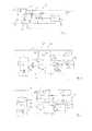
- a chain 11 of LEDs 10, 12, 13, 14, 16, 17, 18, 19 connected in series one to anotheris powered by an inventive driver circuit 20.
- the LEDs 10 to 19 of the chain 11may be used to light outside areas or any other sites which are prone to highly varying temperatures as there are warehouses, cooled stores, lights on ships, aircrafts, stacks, wind turbines, cars, motorcycles, bicycles or the like. It is noted, however, that the invention is not restricted to applications mentioned before. To the contrary, it can be applied to all lighting or signalling applications for indoor and/or outdoor use.
- the chain 11is powered by the driver circuit 20, which supplies current to the LED chain 11 through lines 21 and 22.
- the voltage between the two lines 21, 22is defined by the sum of the forward voltages of all LEDs 10 to 19 of the chain 11.
- the number of LEDsmay be that high that the total forward voltage may exceed 200 volts (e.g. 240 V).
- further chains of LEDsmay be connected in parallel to chain 11.
- groups of LEDsmay be connected in parallel one to another. That, however, does not change anything to the forward voltage which also in those cases may be relatively high and increase with lower temperatures or for other reasons.
- the driver circuit 20comprises a DC power source 23, which provides DC voltage on line 21.
- the other end of the DC voltage source 23is grounded at 24.
- DC voltage source 23may provide a fixed DC voltage which is well above the forward voltage of the chain 11 under all circumstances. This is in particular true if the forward voltage of the LEDs is varying due to external facts like temperature, aging or the like.
- the DC voltage source 23may produce a variable voltage which may be low but still exceeding the forward voltage of the chain 11 if the forward voltage has a first lower value, and which DC voltage is rather high if the forward voltage of the chain 11 is increased for one reason or another. So it can always be made sure that the DC voltage at line 21 exceeds the forward voltage of the chain 11 by all means.
- the DC voltage source 23may be of any suitable type. Preferably, it is powered by the mains supply or any other source, which can be AC or DC of higher or lower voltage.
- DC source 23For connecting with the mains, DC source 23 comprises a mains input 25.
- Any usable power factor correction circuit (PFC)may be used for generating DC power from the alternating mains voltage.
- the power factor correction circuitmay be from the isolating type if desired. It may comprise a rectifier unit and a step-up converter connected thereto. It may be of the fixed output voltage type. Alternatively, it may comprise a control input 26 for receiving a signal S and will adjust the output DC voltage accordingly.
- the current for powering the LED chain 11is supplied by a buck converter 27 drawing current from line 21 through the series connection of the LED chain 11 and an inductor 28.
- the inductor 28may be connected to line 22 as illustrated in Figure 1 or be connected to line 21, alternatively. It may as well be split into two inductors connected to lines 21 and 22, accordingly.
- a diode 29provides a freewheeling part for the LED current I LED and closes a conductive loop.
- the buck converter 27further comprises a switch arrangement 30 comprising a switch for providing a conductive path from line 22 to the ground 24. Further it comprises a drive circuit 31 for controlled closing and opening the switch.
- the drive circuit 31 of the switching arrangement 30comprises at least one input I1, which is connected to a current sensing means 32, which is adapted to sense at least a portion of the current I LED flowing through the LED chain 11.
- Current sensing means 32may be placed at any suitable branch or node of the circuit.
- the controller 31comprises another input I2 for receiving a signal S indicating the forward voltage present at the chain 11.
- the inventive drive circuit 20comprises a mode selector unit 33, which is connected to the LED chain 11 and the control input 12.
- the mode selector unit 33comprises a differential amplifier unit 34 the inputs of which are connected to both ends of the chain 11 e.g. to lines 21 and 22.
- the output of the differential amplifier unit 34is connected to a block 35 which is differential amplifier, for subtraction the reference signal R provided by a block 36 from the output signal V provided by a block 34.
- the output signal of the block 35is a signal S* which is supplied to a block 37.
- Logic block 37passes the signal S* to its output were it appears as signal S. If the signal S*, however, is smaller as, or equal to, zero the output signal S will be zero too.
- the signal Sis supplied to the control input I2 via line 38 and optionally to control input 26, if present.
- DC voltage source 23provides a fairly high voltage of approximately 460 V (DC) or any other suitable value. It is assumed that the forward voltage of the LED chain 11 is well below that value. The forward voltage may be for example 240 V.
- the driver circuit 20assumes a first mode I of operation, which is a current controlled mode of operation.
- the forward voltage across the LED chain 11is sensed by the differential amplifier unit 34, which presents a respective signal to one input of block 35.
- Block 35subtract the reference value R of block 36 from output signal V provided by a block 34. If the output of differential amplifier 34 is smaller than the reference value supplied by block 36 the signal S* is below Zero. If, however, the output of the differential amplifier 34 exceeds the reference value provided by the block 36, the signal S* will be positive and the block 37 will set the signal S equal to S*.
- the forward voltage across the chain 11is below a certain limit.
- the signal V at the output of the differential amplifier 34is smaller than the reference signal R. Consequently no signal S is present on line 38. In terms of block 37 the signal S is zero.
- This statecharacterizes the first mode I of operation.
- the controller 31does not receive a significant control signal from block 37.
- the only thing controller 31 does,is controlling the switch of the buck converter 27 in any suitable way for keeping the average value (or any other feature defining the strength of the current) of the LED current I LED flowing through lines 21 and 22 equal to a desired constant value. Consequently, the first mode I of operation is a current controlled mode.
- the strength of the currentis not dependent in any way from the forward voltage when being in that first mode I of operation. It is noted that the current flowing through the chain 11 is ramping up and down and may be even zero, periodically. However, the mean value thereof is kept constant.
- the driver circuit 20assumes a second mode II of operation.
- the increase of the forward voltagemay be due to very low temperature or other reasons.
- Block 35will now find the output signal V exceeding the reference value R and present a positive interim signal S* at its output. Consequently, the block 37 presents a positive signal S which is fed to the control input I2 line 38.
- the buck converter 27reduces the current fed to the lamp circuit, which is formed by the chain 11 and the inductor 28.
- the reduction of the currentis preferably tuned such that the product of the mean current through the chain 11 and the mean forward voltage is kept to constant desired value.
- Figure 2illustrates a signal V provided by a block 34 indicating the voltage across the LED or chain of LEDs, reference signal R provided by a block 36 and their difference S*.
- Figure 4illustrates the dependency of the LED current I LED and the forward voltage U LED .
- the forward voltage U LEDexceeds a set value R* the first constant current mode of operation or the second constant power mode of operation is assumed.
- the output R of the block 36defines a reference value for the signal V which is related to the forward voltage. The reference value R* however compares directly to the forward voltage.
- Figure 5illustrates the behaviour of the LED current I LED dependent from the forward voltage U LED with dramatically reduced power in the second mode II of operation. While the first mode I of operation is equal to the first modes described before the second mode II* reduces the current more than described before. Consequently, the power supplied to the LED chain 11 will stay below limits and not be constant which, however, may be tolerable or even favourable.
- the line 39is present according to Figure 1
- the DC voltage source 23will keep the DC voltage at line 21 to a somewhat lower value as long as signal S is zero. It will switch the DC voltage to a somewhat higher value at line 21 if the signal S is present and above zero.
- the voltage of the DC source 23 minus the voltage across the chain 11will not exceed a set value of e.g. 20V or 30V in any operating state.
- a set value of e.g. 20V or 30Vin any operating state.
- Figure 6illustrates the basic structure of the inventive driver circuit 20 using a current i signal for representing the signal S.
- the current i signalis fed to a current sensing shunt 40 which is used as the current sensing means 32. Both, the current i signal and the LED current I LED are fed through the shunt 40 which is connected to a signal input IS of the buck converter 27.
- the signal input ISreplaces inputs I1 and I2 of the switching arrangement 30 of figure 1 .
- Further blocks 34, 35 and 37are unified to one single block in figure 6 .
- Block 42 of figure 6transforms the voltage signal into a current signal.
- the driver circuit 20In the first mode I of operation the current i signal is zero. Consequently, the shunt 40 senses just the LED current I LED .
- the driver circuit 20is in the current control mode.
- the current i signalIf the current i signal is positive the current i signal adds to the LED current I LED so that the buck converter tries to keep constant the sum of the LED current I LED and the current i signal. Consequently, it reduces the LED current I LED .
- FIG 7illustrates a somewhat modified embodiment of the driver circuit 20 of figure 6 .
- the buck converter 27uses a switch 41 connected in series with the shunt 40.
- the voltage dropping on the shunt 40is supplied to the control input IS via a resistor R1.
- the current i signalis supplied to the same control input IS via a resistor R2.
- Transforming the signal S into a current i signalis done by U/I converter 42. It uses an operational amplifier in a basically known application.
- Operational amplifier OPA 1is rail-to-rail input/output type with single supply voltage which provides on the output OPA 1 the signal S.
- the blocks 34, 35 and 37are built using at least one operational amplifier in a known wiring.
- two currentsare fed into the input IS which currents are the current i signal and another current defined by the voltage across the shunt 40 and the resistor R1.
- the lattercharacterizes the LED current. If the current i is zero, the controller 31 will operate the switch 41 in a way for keeping the LED current I LED constant. If, however, the current i adds to the current flowing through the resistor R2 the controller 41 will reduce the current flowing through the LED chain 11. Preferably, the reduction is adjusted such that the power supplied to the LED chain 11 will be kept constant.
- a drive circuit 20for powering an LED chain 11 even if the chain presents an unusual high forward voltage drop. This may be due to extraordinary low temperature, connecting more LEDs in the chain, aging or the like. It is considered to raise the DC voltage for powering the LEDs at least if those unusual high voltage drop conditions occur. If so, however, the LED current otherwise kept constant will be reduced in that second mode II of operation. Preferably, the reduction of the LED current is such that the power applied to the LEDs will be kept at a given constant value.
Landscapes
- Circuit Arrangement For Electric Light Sources In General (AREA)
Abstract
Description
- The invention relates generally to a driver circuitry for driving one or several LEDs and in particular to a driver circuitry for driving one or several LEDs for lighting purposes and/or for high power signalling purposes.
- Driving circuits are known for providing current to LEDs by using switches and inductors which are periodically charged from a DC source and discharged to LEDs for providing current to them. Basically it is known to control the power supplied to the LEDs.
WO 2010/118944 A1 discloses a circuitry of the switched inductor type in which the duty cycle of the switch is regulated for controlling the power to the LED. For doing so a signal representing the mean value of the LED current will be compared with a reference value and the duty cycle of the switch will be adjusted accordingly. Alternatively, the signal can be derived from the voltage across the LED. - While it is basically known to regulate the LED current according to the LED voltage or a given reference value, problems may arise if the LEDs are exposed to very low temperatures. The forward voltage of the LEDs increases very much if the LED is exposed to temperatures far below 0°C. The forward voltage may increase such that it reaches or even exceeds the voltage of the DC source the LED current is derived from. As a result it may be that the supply circuitry is not able to power the LEDs under those conditions. If so the LEDs do not light. If this occurs, dangerous situations may result. Increasing the DC voltage, however, can destroy the (very) cold LEDs even if the LED current is limited or kept constant at the rated current.
- It is an object of the present invention to overcome at least one of the problems mentioned before.
- The inventive LED power supply is basically adapted to supply LED current even if the forward voltage of the LEDs is heavily increased e.g. because of low temperatures. It may have an increased internal voltage DC source having a voltage which is higher than the, under worst conditions, largest expectable forward voltage of the LED or chain of LEDs connected to the supply. Even a safety margin may be present so that the DC voltage may be some volts above the highest expectable forward voltage.
- The invention provides that the driver circuit comprises a converter circuit of any usable type. Preferably a buck-type converter is used for supplying current to the LED or chain of LEDs. The converter circuit can be operated in any suitable way, e.g. in a continuous current mode in which the switch is closed before the freewheeling current of the inductor reached zero. It may also be operated in different modes, e.g. the critical mode in which the switch is closed just when the freewheeling current of the inductor reaches Zero. Alternatively, it may be driven in an intermittent mode in which the switch is closed after a small amount of time in which the current remained zero. No matter what mode is used for operating the converter circuitry it may assume two different operational modes. A first mode is used during regular operation if the forward voltage of the LED or chain of LEDs is within an expected normal range. The converter circuit supplies current having a defined mean value to the LEDs in this first mode of operation. Alternatively the converter circuit may supply current having a defined root mean square value (RMS) to the LEDs in this first mode of operation. Furthermore the converter circuit may supply current having any other defined characteristic to the LEDs in this first mode of operation, as there is the peak value or the like.
- The converter circuit may assume a second mode of operation if the forward voltage of the LED or chain of LEDs exceeds a given value. The second mode of operation is defined by supplying a reduced current to the LED or chain of LEDs. By using a reduced LED current in the second mode of operation, a safe operating mode is established. This extends the useful temperature range in which the LEDs may be operated. The LED current may be adjusted such that the LEDs will be safely heated up until reaching sufficient operating temperature and sufficiently low forward voltage. The converter circuit will switch into the first mode of operation if the forward voltage falls below a given reference value.
- In a preferred embodiment the first mode of operation is a constant current operating mode while the second mode of operation may be a constant power operating mode in the sense explained above. The more the forward voltage exceeds the given reference value the lower will be the LED current. It is noted, however, that the second mode of operation may use different approaches. It is possible, for example, to supply a reduced fixed current to the LEDs which, in the second mode of operation, is considerably lower than the current in the first mode of operation.
- In all embodiments it is possible to vary the DC source voltage internally provided for powering and supplying the buck converter. Preferably, the DC voltage is set to a first lower value for operating the driver circuit in the first mode of operation. Further it is preferred to set the DC source to a second higher value for operating the driver circuit in the second mode of operation. The transition may be done stepwise in one single larger or several smaller steps and in a continuous ramping transition process as well. It is also possible to raise the voltage of the DC source in a fixed relation to the LED forward voltage in the second mode of operation. So it is possible to keep constant the difference between the DC source voltage and the LED forward voltage. It is at least possible to keep positive the difference between the DC source voltage and the LED forward voltage.
- Further advantages and aspects of the invention are to be taken from the drawings, the description and dependent claims.
- Embodiments of the invention are to be taken from the drawings in which:
Figure 1 discloses the overall structure of the inventive driver circuit;Figure 2 illustrates a signal indicating the voltage across the LED or chain of LEDs, reference signal and their difference.Figure 3 illustrates a signal indicating the voltage across the LED or chain of LEDs if the voltage exceeds a given reference value;Figure 4 illustrates the current through the LED or chain of LEDS in two different modes of operation of the driver circuit;Figure 5 illustrates the current through the LEDs similar toFigure 3 according to another embodiment;Figure 6 illustrates the basic structure of the inventive buck converter using a current signal for controlling the converter;Figure 7 illustrates the buck converter ofFigure 6 in more details; andFigure 8 illustrates an alternative embodiment of the buck converter ofFigure 6 .- Referring to
Figure 1 at least one LED 10, preferably however, a chain 11 ofLEDs inventive driver circuit 20. The LEDs 10 to 19 of the chain 11 may be used to light outside areas or any other sites which are prone to highly varying temperatures as there are warehouses, cooled stores, lights on ships, aircrafts, stacks, wind turbines, cars, motorcycles, bicycles or the like. It is noted, however, that the invention is not restricted to applications mentioned before. To the contrary, it can be applied to all lighting or signalling applications for indoor and/or outdoor use. - The chain 11 is powered by the
driver circuit 20, which supplies current to the LED chain 11 throughlines lines - The
driver circuit 20 comprises aDC power source 23, which provides DC voltage online 21. The other end of theDC voltage source 23 is grounded at 24.DC voltage source 23 may provide a fixed DC voltage which is well above the forward voltage of the chain 11 under all circumstances. This is in particular true if the forward voltage of the LEDs is varying due to external facts like temperature, aging or the like. However, as an alternative concept in all embodiments disclosed and described above and/or below, theDC voltage source 23 may produce a variable voltage which may be low but still exceeding the forward voltage of the chain 11 if the forward voltage has a first lower value, and which DC voltage is rather high if the forward voltage of the chain 11 is increased for one reason or another. So it can always be made sure that the DC voltage atline 21 exceeds the forward voltage of the chain 11 by all means. - The
DC voltage source 23 may be of any suitable type. Preferably, it is powered by the mains supply or any other source, which can be AC or DC of higher or lower voltage. For connecting with the mains,DC source 23 comprises a mains input 25. Any usable power factor correction circuit (PFC) may be used for generating DC power from the alternating mains voltage. The power factor correction circuit may be from the isolating type if desired. It may comprise a rectifier unit and a step-up converter connected thereto. It may be of the fixed output voltage type. Alternatively, it may comprise acontrol input 26 for receiving a signal S and will adjust the output DC voltage accordingly. - The current for powering the LED chain 11 is supplied by a
buck converter 27 drawing current fromline 21 through the series connection of the LED chain 11 and aninductor 28. Theinductor 28 may be connected to line 22 as illustrated inFigure 1 or be connected toline 21, alternatively. It may as well be split into two inductors connected tolines diode 29 provides a freewheeling part for the LED current ILED and closes a conductive loop. Thebuck converter 27 further comprises aswitch arrangement 30 comprising a switch for providing a conductive path fromline 22 to theground 24. Further it comprises adrive circuit 31 for controlled closing and opening the switch. Thedrive circuit 31 of the switchingarrangement 30 comprises at least one input I1, which is connected to a current sensing means 32, which is adapted to sense at least a portion of the current ILED flowing through the LED chain 11. Current sensing means 32 may be placed at any suitable branch or node of the circuit. - The
controller 31 comprises another input I2 for receiving a signal S indicating the forward voltage present at the chain 11. - The
inventive drive circuit 20 comprises amode selector unit 33, which is connected to the LED chain 11 and thecontrol input 12. Themode selector unit 33 comprises adifferential amplifier unit 34 the inputs of which are connected to both ends of the chain 11 e.g. tolines differential amplifier unit 34 is connected to ablock 35 which is differential amplifier, for subtraction the reference signal R provided by ablock 36 from the output signal V provided by ablock 34. The output signal of theblock 35 is a signal S* which is supplied to ablock 37.Logic block 37 passes the signal S* to its output were it appears as signal S. If the signal S*, however, is smaller as, or equal to, zero the output signal S will be zero too. The signal S is supplied to the control input I2 vialine 38 and optionally to controlinput 26, if present. - In operation,
DC voltage source 23 provides a fairly high voltage of approximately 460 V (DC) or any other suitable value. It is assumed that the forward voltage of the LED chain 11 is well below that value. The forward voltage may be for example 240 V. Thedriver circuit 20 assumes a first mode I of operation, which is a current controlled mode of operation. The forward voltage across the LED chain 11 is sensed by thedifferential amplifier unit 34, which presents a respective signal to one input ofblock 35.Block 35 subtract the reference value R ofblock 36 from output signal V provided by ablock 34. If the output ofdifferential amplifier 34 is smaller than the reference value supplied byblock 36 the signal S* is below Zero. If, however, the output of thedifferential amplifier 34 exceeds the reference value provided by theblock 36, the signal S* will be positive and theblock 37 will set the signal S equal to S*. - In normal operation the forward voltage across the chain 11 is below a certain limit. The signal V at the output of the
differential amplifier 34 is smaller than the reference signal R. Consequently no signal S is present online 38. In terms ofblock 37 the signal S is zero. This state characterizes the first mode I of operation. Thecontroller 31 does not receive a significant control signal fromblock 37. Theonly thing controller 31 does, is controlling the switch of thebuck converter 27 in any suitable way for keeping the average value (or any other feature defining the strength of the current) of the LED current ILED flowing throughlines - If however, for what reason ever, the forward voltage across the chain 11 exceeds a given value, the
driver circuit 20 assumes a second mode II of operation. The increase of the forward voltage may be due to very low temperature or other reasons.Block 35 will now find the output signal V exceeding the reference value R and present a positive interim signal S* at its output. Consequently, theblock 37 presents a positive signal S which is fed to the controlinput I2 line 38. The result being that thebuck converter 27 reduces the current fed to the lamp circuit, which is formed by the chain 11 and theinductor 28. The reduction of the current is preferably tuned such that the product of the mean current through the chain 11 and the mean forward voltage is kept to constant desired value. Figure 2 illustrates a signal V provided by ablock 34 indicating the voltage across the LED or chain of LEDs, reference signal R provided by ablock 36 and their difference S*.- For illustrating the two different modes of operation reference is made to
Figure 3 . While the signal S remains zero (or inactive in any other way) if the forward voltage ULED is below a critical value R* the constant current mode e.g. the first mode I of operation is taken. If however the forward voltage ULED exceeds the given value R* the constant current operational mode e.g. the second mode II of operation is assumed. Figure 4 illustrates the dependency of the LED current ILED and the forward voltage ULED. Depending on whether the forward voltage ULED exceeds a set value R* the first constant current mode of operation or the second constant power mode of operation is assumed. (The output R of theblock 36 defines a reference value for the signal V which is related to the forward voltage. The reference value R* however compares directly to the forward voltage.)- It is noted that numerous modifications can be made on the invention.
Figure 5 illustrates the behaviour of the LED current ILED dependent from the forward voltage ULED with dramatically reduced power in the second mode II of operation. While the first mode I of operation is equal to the first modes described before the second mode II* reduces the current more than described before. Consequently, the power supplied to the LED chain 11 will stay below limits and not be constant which, however, may be tolerable or even favourable. - If, in a modified embodiment, the line 39 is present according to
Figure 1 another modification of the operation is possible. In this case theDC voltage source 23 will keep the DC voltage atline 21 to a somewhat lower value as long as signal S is zero. It will switch the DC voltage to a somewhat higher value atline 21 if the signal S is present and above zero. Alternatively, it is possible to raise the DC voltage atline 21 in proportion to, or otherwise dependent of, signal S on line 39. So it is made sure that the voltage atline 21 is always above the forward voltage ULED across the chain 11, no matter whether the LEDs are very hot or very cold. On the other hand, it is made sure that the voltage of theDC source 23 minus the voltage across the chain 11 will not exceed a set value of e.g. 20V or 30V in any operating state. Thus it is possible to use relatively small inductors and a relatively narrow range of duty cycles and frequencies in theswitch arrangement 30. Figure 6 illustrates the basic structure of theinventive driver circuit 20 using a current i signal for representing the signal S. The current i signal is fed to acurrent sensing shunt 40 which is used as the current sensing means 32. Both, the current i signal and the LED current ILED are fed through theshunt 40 which is connected to a signal input IS of thebuck converter 27. The signal input IS replaces inputs I1 and I2 of the switchingarrangement 30 offigure 1 . Further blocks 34, 35 and 37 are unified to one single block infigure 6 .Block 42 offigure 6 transforms the voltage signal into a current signal.- In the first mode I of operation the current i signal is zero. Consequently, the
shunt 40 senses just the LED current ILED. Thedriver circuit 20 is in the current control mode. - If the current i signal is positive the current i signal adds to the LED current ILED so that the buck converter tries to keep constant the sum of the LED current ILED and the current i signal. Consequently, it reduces the LED current ILED.
Figure 7 illustrates a somewhat modified embodiment of thedriver circuit 20 offigure 6 . Thebuck converter 27 uses aswitch 41 connected in series with theshunt 40. The voltage dropping on theshunt 40 is supplied to the control input IS via a resistor R1. The current i signal is supplied to the same control input IS via a resistor R2. Transforming the signal S into a current i signal is done by U/I converter 42. It uses an operational amplifier in a basically known application.Operational amplifier OPA 1 is rail-to-rail input/output type with single supply voltage which provides on theoutput OPA 1 the signal S.- Similarly, the
blocks - As can be seen, two currents are fed into the input IS which currents are the current i signal and another current defined by the voltage across the
shunt 40 and the resistor R1. The latter characterizes the LED current. If the current i is zero, thecontroller 31 will operate theswitch 41 in a way for keeping the LED current ILED constant. If, however, the current i adds to the current flowing through the resistor R2 thecontroller 41 will reduce the current flowing through the LED chain 11. Preferably, the reduction is adjusted such that the power supplied to the LED chain 11 will be kept constant. - The same is true for the modified buck converter illustrated in
figure 8 . The only difference is to be found in the wiring of the LED chain 11, thediode 29, theinductor 28 and theswitch 41. However, the description given toFigure 1 to 7 totally applies to the modified buck converter ofFigure 7 in regard to the structural description and to the functional description as well. - A
drive circuit 20 is disclosed for powering an LED chain 11 even if the chain presents an unusual high forward voltage drop. This may be due to extraordinary low temperature, connecting more LEDs in the chain, aging or the like. It is considered to raise the DC voltage for powering the LEDs at least if those unusual high voltage drop conditions occur. If so, however, the LED current otherwise kept constant will be reduced in that second mode II of operation. Preferably, the reduction of the LED current is such that the power applied to the LEDs will be kept at a given constant value. - 10
- LED
- 11
- chain of LEDs
- 12 ― 19
- LEDs
- 20
- Driver Circuit
- 21
- Line
- 22
- Line
- 23
- DC Voltage Source
- 24
- Ground
- 25
- Mains Input
- 26
- Control Input
- 27
- Buck Converter
- 28
- Inductor
- 29
- Diode
- 30
- Switching Arrangement
- 31
- Controller
- 32
- Current Sensig Means
- i1
- Current Sensing Input
- i2
- Control Input
- is
- Current Sensing Input
- 33
- Mode Selecting Unit
- 34
Differential Amplifier Unit 1- 35
- Differential Amplifier Unit 2
- 36
- Reference Value Block
- 37
- Block
- 38
- Line
- 39
- Line
- 40
- Shunt
- 41
- Switch
- 42
- V/I Converter
Claims (14)
- Driver circuit (20) for driving an LED (10) or a chain of LEDs (11) for signalling or lighting purposes comprising:a converter circuit (27) adapted to supply to the LED (10) or chain (11) of LEDs i) constant current in a first mode (I) of operation and ii) decreased current in a second mode (II) of operation;a mode selecting unit (33) for producing a signal (i, s) indicating the voltage (ULED) across the LED (10) or chain (11) of LEDs if the voltage (ULED) or a signal (V) derived therefrom exceeds a given reference value (R);the converter circuit (27) comprising an input (i2, is) being connected to the sensing circuit (34) for receiving the signal (i, s), wherein the converter circuit (27) is operated in the first mode (I) of operation, if the signal (i, s) indicates the voltage (ULED) or the signal (V) derived therefrom being below the given reference value (R), and wherein the converter circuit (27) is operated in the second mode (II) of operation, if the signal (i, s) indicates the voltage (ULED) or the signal (V) derived therefrom being above the given reference value (R).
- Driver circuit according to claim 1, wherein the mode selecting unit (33) comprises a differential amplifier (34, OPA1) having a first input (+) connected to anode of the LED (10) or chain (11) of LEDs and having another input (-) connected to cathode of the LED (10) or chain (11) of LEDs.
- Driver circuit according to one of the preceding claims, wherein the mode selecting unit (33) comprises a differential amplifier (35) having at least one input for receiving a signal (V) which is proportional to the voltage across the LED (10) or chain (11) of LEDs and another input for receiving the reference signal (R).
- Driver circuit according to one of the preceding claims, wherein a module (37) is provided for setting the signal (i, s) to zero if the voltage across the LED (10) or chain (11) of LEDs or the signal (V) derived therefrom does not exceed the given value (R).
- Driver circuit according to one of the preceding claims, wherein a module (37) is provided for setting the signal (i, s) to a positive nonzero value, if the voltage across the LED (10) or chain (11) of LEDs or the signal (V) derived therefrom does exceed the given value (R).
- Driver circuit according to one of the preceding claims, wherein a module (37) is provided for setting the signal (i, s) to a value, which is proportional to the difference between the voltage across the LED (10) or chain (11) of LEDs or the signal (V) derived therefrom, and the given reference value (R), if the voltage across the LED (10) or chain (11) of LEDs or the signal (V) derived therefrom does exceed the given value.
- Driver circuit according to one of the preceding claims, wherein the signal (s) is an electrical current (i).
- Driver circuit according to one of the preceding claims, wherein the converter circuit (27) comprises a current sensing input (is) connected to a shunt (40) the LED (10) or chain (11) of LEDs current is fed to.
- Driver circuit according to claims 7 and 8, wherein the signal (i, s) is fed to the current sensing input (i2, is) whereby the signal (i) current adds to a signal caused by the LED current (ILED).
- Driver circuit according to one of the preceding claims, wherein the decreased current (ILED) is adjusted such that any power produced by the LED (10) or chain (11) of LEDs will not exceed a set maximum power in any operating state.
- Driver circuit according to one of the preceding claims, wherein the supply circuit (20), in the second mode (II) of operation, supplies constant power to the LED (10) or chain (11) of LEDs.
- Method for driving an LED (10) or a chain (11) of LED for lighting and signalling purposes comprising:sensing the voltage across the LED (10) or chain (11) of LEDs,supplying to at least one LED (10) or chain (11) of LEDs constant current (ILED) if the voltage (ULED) or a signal (V) derived therefrom is below a given reference value (R),supplying to at least one LED (10) or chain (11) of LEDs decreased current (ILED) if the voltage (ULED) or a signal (V) derived therefrom is above the given reference value (R).
- Method according to claim 12,characterized by
providing a signal (s) which is neutral if the voltage (ULED) across the LED (10) or chain (11) of LEDs or a signal (V) derived therefrom is below the reference value (R) and which is different from zero and proportional to Voltage (ULED) across the LED (10) or chain (11) of LEDs if the Voltage (ULED) across the LED (10) or chain (11) of LEDs or a signal (V) derived therefrom is above the reference value (R), and
adding the signal (s) to another signal derived from the current flowing through the LED (10) or chain (11) of LEDs. - Method according to claim 12,characterized by
providing a current (i) which is zero if the voltage (ULED) across the LED (10) or chain (11) of LEDs or a signal (V) derived therefrom is below the reference value (R) and which is different from zero and proportional to Voltage (ULED) across the LED (10) or chain (11) of LEDs if the Voltage (ULED) across the LED (10) or chain (11) of LEDs or a signal (V) derived therefrom is above the reference value (R), and
adding the current (i) to another current derived from a voltage caused by a current flowing through a shunt (40) and characterizing the current (ILED) flowing through the LED (10) or chain (11) of LEDs.
Priority Applications (1)
| Application Number | Priority Date | Filing Date | Title |
|---|---|---|---|
| EP11191353.9AEP2600694B1 (en) | 2011-11-30 | 2011-11-30 | LED driver circuit with constant power safe operating area |
Applications Claiming Priority (1)
| Application Number | Priority Date | Filing Date | Title |
|---|---|---|---|
| EP11191353.9AEP2600694B1 (en) | 2011-11-30 | 2011-11-30 | LED driver circuit with constant power safe operating area |
Publications (2)
| Publication Number | Publication Date |
|---|---|
| EP2600694A1true EP2600694A1 (en) | 2013-06-05 |
| EP2600694B1 EP2600694B1 (en) | 2013-11-20 |
Family
ID=45047664
Family Applications (1)
| Application Number | Title | Priority Date | Filing Date |
|---|---|---|---|
| EP11191353.9ANot-in-forceEP2600694B1 (en) | 2011-11-30 | 2011-11-30 | LED driver circuit with constant power safe operating area |
Country Status (1)
| Country | Link |
|---|---|
| EP (1) | EP2600694B1 (en) |
Cited By (1)
| Publication number | Priority date | Publication date | Assignee | Title |
|---|---|---|---|---|
| WO2021013699A1 (en)* | 2019-07-24 | 2021-01-28 | Eldolab Holding B.V. | Smart starting up method by an led driver |
Citations (5)
| Publication number | Priority date | Publication date | Assignee | Title |
|---|---|---|---|---|
| EP0482520A1 (en)* | 1990-10-20 | 1992-04-29 | Fujitsu Limited | Constant-current circuit for light-emitting element |
| US20040155844A1 (en)* | 2003-02-07 | 2004-08-12 | Whelen Engineering Company, Inc. | LED driver circuits |
| WO2010025450A2 (en)* | 2008-08-29 | 2010-03-04 | Cirrus Logic, Inc | Led lighting system with accurate current control |
| WO2010118944A1 (en) | 2009-04-14 | 2010-10-21 | Tridonic Gmbh & Co Kg | Power regulation of led by means of an average value the led current and bidirectional counter |
| US20110254530A1 (en)* | 2010-04-14 | 2011-10-20 | Hulett Jeffery Neil | Fault protected current source for lighting element testing |
- 2011
- 2011-11-30EPEP11191353.9Apatent/EP2600694B1/ennot_activeNot-in-force
Patent Citations (5)
| Publication number | Priority date | Publication date | Assignee | Title |
|---|---|---|---|---|
| EP0482520A1 (en)* | 1990-10-20 | 1992-04-29 | Fujitsu Limited | Constant-current circuit for light-emitting element |
| US20040155844A1 (en)* | 2003-02-07 | 2004-08-12 | Whelen Engineering Company, Inc. | LED driver circuits |
| WO2010025450A2 (en)* | 2008-08-29 | 2010-03-04 | Cirrus Logic, Inc | Led lighting system with accurate current control |
| WO2010118944A1 (en) | 2009-04-14 | 2010-10-21 | Tridonic Gmbh & Co Kg | Power regulation of led by means of an average value the led current and bidirectional counter |
| US20110254530A1 (en)* | 2010-04-14 | 2011-10-20 | Hulett Jeffery Neil | Fault protected current source for lighting element testing |
Cited By (5)
| Publication number | Priority date | Publication date | Assignee | Title |
|---|---|---|---|---|
| WO2021013699A1 (en)* | 2019-07-24 | 2021-01-28 | Eldolab Holding B.V. | Smart starting up method by an led driver |
| NL2023562B1 (en)* | 2019-07-24 | 2021-02-10 | Eldolab Holding Bv | Smart starting up method by an LED driver |
| US20220322510A1 (en)* | 2019-07-24 | 2022-10-06 | Eldolab Holding B.V. | Smart starting up method by an led driver |
| EP4005348B1 (en) | 2019-07-24 | 2023-05-31 | eldoLAB Holding B.V. | Smart starting up method by an led driver |
| US11825578B2 (en)* | 2019-07-24 | 2023-11-21 | Eldolab Holding B.V. | Smart starting up method by an LED driver |
Also Published As
| Publication number | Publication date |
|---|---|
| EP2600694B1 (en) | 2013-11-20 |
Similar Documents
| Publication | Publication Date | Title |
|---|---|---|
| US9769887B2 (en) | Power converter for an LED assembly and lighting application | |
| US9313851B2 (en) | Standby power for LED drivers | |
| EP2214457B1 (en) | Led dimming apparatus | |
| CN102907173B (en) | With with the LED manipulation portion of the constant-current source of clock signal duty | |
| CN103582240B (en) | Control the light adjusting controller of LED light source, drive circuit and light-dimming method | |
| CN104349548B (en) | Ignition device and ligthing paraphernalia | |
| CN102427633A (en) | Circuits and methods for driving light sources | |
| WO2011071637A1 (en) | Electronic driver dimming control using ramped pulsed modulation for large area solid-state oleds | |
| CN104640300A (en) | Light source drive circuit, color temperature controller and method for controlling light source color temperature | |
| CN103260303A (en) | Portable lighting device, and method and controller for controlling power supply to load | |
| CN103535114B (en) | LED retrofit driver circuit and method of operating it | |
| JP2010135473A (en) | Light-emitting diode driving power supply unit | |
| KR101043476B1 (en) | PMM dimming drive circuit for LEDs | |
| Lu et al. | High efficiency adaptive boost converter for LED drivers | |
| Pinto et al. | A bidirectional buck-boost converter to supply LEDs from batteries during peak load time | |
| US10271391B2 (en) | Light emitting diode driver | |
| US9078317B1 (en) | Floating output voltage boost regulator driving LEDs using a buck controller | |
| CN103068103A (en) | Power supply device and driving device | |
| CN209748857U (en) | Centralized power supply type LED driving system | |
| EP2600694B1 (en) | LED driver circuit with constant power safe operating area | |
| CN203206526U (en) | Light-emitting diode (LED) lighting device with certain power | |
| JP5562081B2 (en) | LED dimming method and dimming device | |
| CN107113930B (en) | The ripple in the light bulb based on light emitting diode (LED) is reduced by increasing the ripple in energy storage capacitor | |
| JP2011151504A (en) | Load drive controller | |
| EP3207765B1 (en) | A lighting controller, a lighting system and a method for controlling lighting |
Legal Events
| Date | Code | Title | Description |
|---|---|---|---|
| PUAI | Public reference made under article 153(3) epc to a published international application that has entered the european phase | Free format text:ORIGINAL CODE: 0009012 | |
| AK | Designated contracting states | Kind code of ref document:A1 Designated state(s):AL AT BE BG CH CY CZ DE DK EE ES FI FR GB GR HR HU IE IS IT LI LT LU LV MC MK MT NL NO PL PT RO RS SE SI SK SM TR | |
| AX | Request for extension of the european patent | Extension state:BA ME | |
| 17P | Request for examination filed | Effective date:20130701 | |
| RBV | Designated contracting states (corrected) | Designated state(s):AL AT BE BG CH CY CZ DE DK EE ES FI FR GB GR HR HU IE IS IT LI LT LU LV MC MK MT NL NO PL PT RO RS SE SI SK SM TR | |
| GRAP | Despatch of communication of intention to grant a patent | Free format text:ORIGINAL CODE: EPIDOSNIGR1 | |
| RIC1 | Information provided on ipc code assigned before grant | Ipc:H05B 33/08 20060101AFI20130807BHEP | |
| INTG | Intention to grant announced | Effective date:20130912 | |
| GRAS | Grant fee paid | Free format text:ORIGINAL CODE: EPIDOSNIGR3 | |
| GRAA | (expected) grant | Free format text:ORIGINAL CODE: 0009210 | |
| AK | Designated contracting states | Kind code of ref document:B1 Designated state(s):AL AT BE BG CH CY CZ DE DK EE ES FI FR GB GR HR HU IE IS IT LI LT LU LV MC MK MT NL NO PL PT RO RS SE SI SK SM TR | |
| REG | Reference to a national code | Ref country code:GB Ref legal event code:FG4D | |
| REG | Reference to a national code | Ref country code:CH Ref legal event code:EP | |
| REG | Reference to a national code | Ref country code:AT Ref legal event code:REF Ref document number:642285 Country of ref document:AT Kind code of ref document:T Effective date:20131215 | |
| REG | Reference to a national code | Ref country code:IE Ref legal event code:FG4D | |
| REG | Reference to a national code | Ref country code:DE Ref legal event code:R096 Ref document number:602011003844 Country of ref document:DE Effective date:20140116 | |
| PGFP | Annual fee paid to national office [announced via postgrant information from national office to epo] | Ref country code:FR Payment date:20131128 Year of fee payment:3 | |
| REG | Reference to a national code | Ref country code:NL Ref legal event code:VDEP Effective date:20131120 | |
| REG | Reference to a national code | Ref country code:AT Ref legal event code:MK05 Ref document number:642285 Country of ref document:AT Kind code of ref document:T Effective date:20131120 | |
| REG | Reference to a national code | Ref country code:LT Ref legal event code:MG4D | |
| PG25 | Lapsed in a contracting state [announced via postgrant information from national office to epo] | Ref country code:HR Free format text:LAPSE BECAUSE OF FAILURE TO SUBMIT A TRANSLATION OF THE DESCRIPTION OR TO PAY THE FEE WITHIN THE PRESCRIBED TIME-LIMIT Effective date:20131120 Ref country code:NL Free format text:LAPSE BECAUSE OF FAILURE TO SUBMIT A TRANSLATION OF THE DESCRIPTION OR TO PAY THE FEE WITHIN THE PRESCRIBED TIME-LIMIT Effective date:20131120 Ref country code:LT Free format text:LAPSE BECAUSE OF FAILURE TO SUBMIT A TRANSLATION OF THE DESCRIPTION OR TO PAY THE FEE WITHIN THE PRESCRIBED TIME-LIMIT Effective date:20131120 Ref country code:IS Free format text:LAPSE BECAUSE OF FAILURE TO SUBMIT A TRANSLATION OF THE DESCRIPTION OR TO PAY THE FEE WITHIN THE PRESCRIBED TIME-LIMIT Effective date:20140320 Ref country code:FI Free format text:LAPSE BECAUSE OF FAILURE TO SUBMIT A TRANSLATION OF THE DESCRIPTION OR TO PAY THE FEE WITHIN THE PRESCRIBED TIME-LIMIT Effective date:20131120 Ref country code:SE Free format text:LAPSE BECAUSE OF FAILURE TO SUBMIT A TRANSLATION OF THE DESCRIPTION OR TO PAY THE FEE WITHIN THE PRESCRIBED TIME-LIMIT Effective date:20131120 Ref country code:NO Free format text:LAPSE BECAUSE OF FAILURE TO SUBMIT A TRANSLATION OF THE DESCRIPTION OR TO PAY THE FEE WITHIN THE PRESCRIBED TIME-LIMIT Effective date:20140220 | |
| PG25 | Lapsed in a contracting state [announced via postgrant information from national office to epo] | Ref country code:LV Free format text:LAPSE BECAUSE OF FAILURE TO SUBMIT A TRANSLATION OF THE DESCRIPTION OR TO PAY THE FEE WITHIN THE PRESCRIBED TIME-LIMIT Effective date:20131120 Ref country code:RS Free format text:LAPSE BECAUSE OF FAILURE TO SUBMIT A TRANSLATION OF THE DESCRIPTION OR TO PAY THE FEE WITHIN THE PRESCRIBED TIME-LIMIT Effective date:20131120 Ref country code:AT Free format text:LAPSE BECAUSE OF FAILURE TO SUBMIT A TRANSLATION OF THE DESCRIPTION OR TO PAY THE FEE WITHIN THE PRESCRIBED TIME-LIMIT Effective date:20131120 Ref country code:BE Free format text:LAPSE BECAUSE OF FAILURE TO SUBMIT A TRANSLATION OF THE DESCRIPTION OR TO PAY THE FEE WITHIN THE PRESCRIBED TIME-LIMIT Effective date:20131120 Ref country code:ES Free format text:LAPSE BECAUSE OF FAILURE TO SUBMIT A TRANSLATION OF THE DESCRIPTION OR TO PAY THE FEE WITHIN THE PRESCRIBED TIME-LIMIT Effective date:20131120 | |
| PG25 | Lapsed in a contracting state [announced via postgrant information from national office to epo] | Ref country code:PT Free format text:LAPSE BECAUSE OF FAILURE TO SUBMIT A TRANSLATION OF THE DESCRIPTION OR TO PAY THE FEE WITHIN THE PRESCRIBED TIME-LIMIT Effective date:20140320 | |
| PG25 | Lapsed in a contracting state [announced via postgrant information from national office to epo] | Ref country code:EE Free format text:LAPSE BECAUSE OF FAILURE TO SUBMIT A TRANSLATION OF THE DESCRIPTION OR TO PAY THE FEE WITHIN THE PRESCRIBED TIME-LIMIT Effective date:20131120 | |
| REG | Reference to a national code | Ref country code:DE Ref legal event code:R097 Ref document number:602011003844 Country of ref document:DE | |
| REG | Reference to a national code | Ref country code:IE Ref legal event code:MM4A | |
| PG25 | Lapsed in a contracting state [announced via postgrant information from national office to epo] | Ref country code:IT Free format text:LAPSE BECAUSE OF FAILURE TO SUBMIT A TRANSLATION OF THE DESCRIPTION OR TO PAY THE FEE WITHIN THE PRESCRIBED TIME-LIMIT Effective date:20131120 Ref country code:SK Free format text:LAPSE BECAUSE OF FAILURE TO SUBMIT A TRANSLATION OF THE DESCRIPTION OR TO PAY THE FEE WITHIN THE PRESCRIBED TIME-LIMIT Effective date:20131120 Ref country code:PL Free format text:LAPSE BECAUSE OF FAILURE TO SUBMIT A TRANSLATION OF THE DESCRIPTION OR TO PAY THE FEE WITHIN THE PRESCRIBED TIME-LIMIT Effective date:20131120 Ref country code:CZ Free format text:LAPSE BECAUSE OF FAILURE TO SUBMIT A TRANSLATION OF THE DESCRIPTION OR TO PAY THE FEE WITHIN THE PRESCRIBED TIME-LIMIT Effective date:20131120 Ref country code:RO Free format text:LAPSE BECAUSE OF FAILURE TO SUBMIT A TRANSLATION OF THE DESCRIPTION OR TO PAY THE FEE WITHIN THE PRESCRIBED TIME-LIMIT Effective date:20131120 | |
| PLBE | No opposition filed within time limit | Free format text:ORIGINAL CODE: 0009261 | |
| STAA | Information on the status of an ep patent application or granted ep patent | Free format text:STATUS: NO OPPOSITION FILED WITHIN TIME LIMIT | |
| PG25 | Lapsed in a contracting state [announced via postgrant information from national office to epo] | Ref country code:DK Free format text:LAPSE BECAUSE OF FAILURE TO SUBMIT A TRANSLATION OF THE DESCRIPTION OR TO PAY THE FEE WITHIN THE PRESCRIBED TIME-LIMIT Effective date:20131120 | |
| 26N | No opposition filed | Effective date:20140821 | |
| PG25 | Lapsed in a contracting state [announced via postgrant information from national office to epo] | Ref country code:IE Free format text:LAPSE BECAUSE OF NON-PAYMENT OF DUE FEES Effective date:20131130 | |
| REG | Reference to a national code | Ref country code:DE Ref legal event code:R097 Ref document number:602011003844 Country of ref document:DE Effective date:20140821 | |
| PG25 | Lapsed in a contracting state [announced via postgrant information from national office to epo] | Ref country code:SI Free format text:LAPSE BECAUSE OF FAILURE TO SUBMIT A TRANSLATION OF THE DESCRIPTION OR TO PAY THE FEE WITHIN THE PRESCRIBED TIME-LIMIT Effective date:20131120 | |
| PG25 | Lapsed in a contracting state [announced via postgrant information from national office to epo] | Ref country code:MC Free format text:LAPSE BECAUSE OF FAILURE TO SUBMIT A TRANSLATION OF THE DESCRIPTION OR TO PAY THE FEE WITHIN THE PRESCRIBED TIME-LIMIT Effective date:20131120 | |
| PG25 | Lapsed in a contracting state [announced via postgrant information from national office to epo] | Ref country code:CY Free format text:LAPSE BECAUSE OF FAILURE TO SUBMIT A TRANSLATION OF THE DESCRIPTION OR TO PAY THE FEE WITHIN THE PRESCRIBED TIME-LIMIT Effective date:20131120 Ref country code:SM Free format text:LAPSE BECAUSE OF FAILURE TO SUBMIT A TRANSLATION OF THE DESCRIPTION OR TO PAY THE FEE WITHIN THE PRESCRIBED TIME-LIMIT Effective date:20131120 | |
| REG | Reference to a national code | Ref country code:CH Ref legal event code:PL | |
| PG25 | Lapsed in a contracting state [announced via postgrant information from national office to epo] | Ref country code:HU Free format text:LAPSE BECAUSE OF FAILURE TO SUBMIT A TRANSLATION OF THE DESCRIPTION OR TO PAY THE FEE WITHIN THE PRESCRIBED TIME-LIMIT; INVALID AB INITIO Effective date:20111130 Ref country code:LU Free format text:LAPSE BECAUSE OF NON-PAYMENT OF DUE FEES Effective date:20131130 Ref country code:MK Free format text:LAPSE BECAUSE OF FAILURE TO SUBMIT A TRANSLATION OF THE DESCRIPTION OR TO PAY THE FEE WITHIN THE PRESCRIBED TIME-LIMIT Effective date:20131120 Ref country code:LI Free format text:LAPSE BECAUSE OF NON-PAYMENT OF DUE FEES Effective date:20141130 Ref country code:BG Free format text:LAPSE BECAUSE OF FAILURE TO SUBMIT A TRANSLATION OF THE DESCRIPTION OR TO PAY THE FEE WITHIN THE PRESCRIBED TIME-LIMIT Effective date:20131120 Ref country code:CH Free format text:LAPSE BECAUSE OF NON-PAYMENT OF DUE FEES Effective date:20141130 | |
| REG | Reference to a national code | Ref country code:FR Ref legal event code:ST Effective date:20150731 | |
| PG25 | Lapsed in a contracting state [announced via postgrant information from national office to epo] | Ref country code:GR Free format text:LAPSE BECAUSE OF NON-PAYMENT OF DUE FEES Effective date:20131120 Ref country code:MT Free format text:LAPSE BECAUSE OF FAILURE TO SUBMIT A TRANSLATION OF THE DESCRIPTION OR TO PAY THE FEE WITHIN THE PRESCRIBED TIME-LIMIT Effective date:20131120 | |
| PG25 | Lapsed in a contracting state [announced via postgrant information from national office to epo] | Ref country code:FR Free format text:LAPSE BECAUSE OF NON-PAYMENT OF DUE FEES Effective date:20141201 | |
| PG25 | Lapsed in a contracting state [announced via postgrant information from national office to epo] | Ref country code:GR Free format text:LAPSE BECAUSE OF FAILURE TO SUBMIT A TRANSLATION OF THE DESCRIPTION OR TO PAY THE FEE WITHIN THE PRESCRIBED TIME-LIMIT Effective date:20140221 | |
| GBPC | Gb: european patent ceased through non-payment of renewal fee | Effective date:20151130 | |
| PG25 | Lapsed in a contracting state [announced via postgrant information from national office to epo] | Ref country code:TR Free format text:LAPSE BECAUSE OF FAILURE TO SUBMIT A TRANSLATION OF THE DESCRIPTION OR TO PAY THE FEE WITHIN THE PRESCRIBED TIME-LIMIT Effective date:20131120 | |
| PG25 | Lapsed in a contracting state [announced via postgrant information from national office to epo] | Ref country code:GB Free format text:LAPSE BECAUSE OF NON-PAYMENT OF DUE FEES Effective date:20151130 | |
| PG25 | Lapsed in a contracting state [announced via postgrant information from national office to epo] | Ref country code:AL Free format text:LAPSE BECAUSE OF FAILURE TO SUBMIT A TRANSLATION OF THE DESCRIPTION OR TO PAY THE FEE WITHIN THE PRESCRIBED TIME-LIMIT Effective date:20131120 | |
| REG | Reference to a national code | Ref country code:DE Ref legal event code:R079 Ref document number:602011003844 Country of ref document:DE Free format text:PREVIOUS MAIN CLASS: H05B0033080000 Ipc:H05B0045000000 | |
| PGFP | Annual fee paid to national office [announced via postgrant information from national office to epo] | Ref country code:DE Payment date:20201130 Year of fee payment:10 | |
| REG | Reference to a national code | Ref country code:DE Ref legal event code:R119 Ref document number:602011003844 Country of ref document:DE | |
| PG25 | Lapsed in a contracting state [announced via postgrant information from national office to epo] | Ref country code:DE Free format text:LAPSE BECAUSE OF NON-PAYMENT OF DUE FEES Effective date:20220601 |