EP2596525B1 - Handling device for handling a wafer - Google Patents
Handling device for handling a waferDownload PDFInfo
- Publication number
- EP2596525B1 EP2596525B1EP10737783.0AEP10737783AEP2596525B1EP 2596525 B1EP2596525 B1EP 2596525B1EP 10737783 AEP10737783 AEP 10737783AEP 2596525 B1EP2596525 B1EP 2596525B1
- Authority
- EP
- European Patent Office
- Prior art keywords
- wafer
- cover
- handling
- handling device
- grid structure
- Prior art date
- Legal status (The legal status is an assumption and is not a legal conclusion. Google has not performed a legal analysis and makes no representation as to the accuracy of the status listed.)
- Active
Links
Images

Classifications
- H—ELECTRICITY
- H01—ELECTRIC ELEMENTS
- H01L—SEMICONDUCTOR DEVICES NOT COVERED BY CLASS H10
- H01L21/00—Processes or apparatus adapted for the manufacture or treatment of semiconductor or solid state devices or of parts thereof
- H01L21/67—Apparatus specially adapted for handling semiconductor or electric solid state devices during manufacture or treatment thereof; Apparatus specially adapted for handling wafers during manufacture or treatment of semiconductor or electric solid state devices or components ; Apparatus not specifically provided for elsewhere
- H01L21/683—Apparatus specially adapted for handling semiconductor or electric solid state devices during manufacture or treatment thereof; Apparatus specially adapted for handling wafers during manufacture or treatment of semiconductor or electric solid state devices or components ; Apparatus not specifically provided for elsewhere for supporting or gripping
- H01L21/6838—Apparatus specially adapted for handling semiconductor or electric solid state devices during manufacture or treatment thereof; Apparatus specially adapted for handling wafers during manufacture or treatment of semiconductor or electric solid state devices or components ; Apparatus not specifically provided for elsewhere for supporting or gripping with gripping and holding devices using a vacuum; Bernoulli devices
- H—ELECTRICITY
- H01—ELECTRIC ELEMENTS
- H01L—SEMICONDUCTOR DEVICES NOT COVERED BY CLASS H10
- H01L21/00—Processes or apparatus adapted for the manufacture or treatment of semiconductor or solid state devices or of parts thereof
- H01L21/67—Apparatus specially adapted for handling semiconductor or electric solid state devices during manufacture or treatment thereof; Apparatus specially adapted for handling wafers during manufacture or treatment of semiconductor or electric solid state devices or components ; Apparatus not specifically provided for elsewhere
- H01L21/683—Apparatus specially adapted for handling semiconductor or electric solid state devices during manufacture or treatment thereof; Apparatus specially adapted for handling wafers during manufacture or treatment of semiconductor or electric solid state devices or components ; Apparatus not specifically provided for elsewhere for supporting or gripping
- H01L21/687—Apparatus specially adapted for handling semiconductor or electric solid state devices during manufacture or treatment thereof; Apparatus specially adapted for handling wafers during manufacture or treatment of semiconductor or electric solid state devices or components ; Apparatus not specifically provided for elsewhere for supporting or gripping using mechanical means, e.g. chucks, clamps or pinches
- H01L21/68714—Apparatus specially adapted for handling semiconductor or electric solid state devices during manufacture or treatment thereof; Apparatus specially adapted for handling wafers during manufacture or treatment of semiconductor or electric solid state devices or components ; Apparatus not specifically provided for elsewhere for supporting or gripping using mechanical means, e.g. chucks, clamps or pinches the wafers being placed on a susceptor, stage or support
- H01L21/68735—Apparatus specially adapted for handling semiconductor or electric solid state devices during manufacture or treatment thereof; Apparatus specially adapted for handling wafers during manufacture or treatment of semiconductor or electric solid state devices or components ; Apparatus not specifically provided for elsewhere for supporting or gripping using mechanical means, e.g. chucks, clamps or pinches the wafers being placed on a susceptor, stage or support characterised by edge profile or support profile
Definitions
- the present inventionrelates to a handling device for handling a wafer when processing the wafer according to claim 1.
- the US 2007/0026772 A1describes a generic device for use in processing a semiconductor workpiece.
- the fixing of wafers by means of electrostatic chargingleads to partially unwanted discharge of the carrier and / or the wafer.
- the object of the present inventionis to provide a handling device for the handling of wafers, with which a safe and easy handling of a wafer in the most gentle and non-destructive manner is possible.
- the technical problemshould be solved that the wafer is residue-free from the handling device solvable without damaging the wafer and without much effort.
- the inventionis based on the idea to provide for a handling device, a wafer only partially supporting spacers, which is formed by means of a cover, in particular a cover and by applying a negative pressure to the environment so that the contact surface of the cover is reduced with the wafer , As a result, the adhesive force is reduced, so that the wafer can be removed in a simple manner and non-destructive and residue-free from the cover.
- the handlingis environmentally friendly only by pressure change and thus energetically particularly economical.
- the carrier according to the inventionmakes it possible to fix ultra-thin wafers, in particular wafers with components on the surface, in areas without components on the surface, so that the particularly sensitive and expensive parts of the wafer are spared and a fixation of the wafer, in particular at the edge, in Areas that may even be specifically designed for this purpose.
- the wafercan be removed without residue, without damage and with extremely little effort from the carrier or the adhesive cover.
- the handling devicecan be reused, in particular for more than 10, preferably more than 100, particularly preferably more than 1000 handling operations.
- the grid structureis annular, in particular annular, preferably with a ratio of the ring width B to the diameter D of the grid structure of less than 1: 5, in particular less than 1:10, preferably less than 1:15, is trained.
- the coveris a, in particular adhesive, film, preferably a gel film
- the handlingin particular the release of the wafer, in a simple manner without chemical solvents or without temperature influence, so that the resources are spared.
- PDMSpolydimenthylsiloxane
- PFPEperfluoropolyether
- the fixationtakes place exclusively in a region of the wafer without raised structures, in particular on the edge of the wafer.
- the raised structures of the waferare spared and allows a tension-free recording of the wafer.
- a use of the handling device within wafer processing devicesis to be considered which processes wafers under reduced pressure. It is particularly advantageous if the grid space can be acted upon by a higher negative pressure than the negative pressure in the wafer processing device.
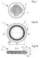
- FIG. 1 1shows a wafer 1 with a region of the wafer 1 with raised structures 4, in particular chips, and a region of the wafer 1 without raised structures, namely an edge region 3 of the wafer 1, which is used for fixing the wafer 1 to an in FIG. 2a shown handling device 5 is used.
- the raised structures 4are on a wafer receiving side 2, which comes into contact with the edge region 3 at a contact surface 14 on a handling device 5.
- the handling device 5consists of a carrier 6, here a chuck, on which a grid structure 8 is applied, namely on a flat receiving side 11, which in the in FIG. 2b is shown above.
- the raster structure 8is according to FIG. 2a circular and is from the receiving side 11 of the carrier 6 from.
- the grid structure 8is connected to the carrier 6, either embedded, welded or glued.
- the grid structure 8has no closed surface and is coated with a cover 7 formed as a gel film and the cover 7 is thus also annular and in the embodiment shown here laterally fixed by the grid structure 8 on the support 6, here on the receiving side 11, and tightly sealed , It is also conceivable that the film covering the entire receiving side 11 and is fixed to the side or bottom of the carrier 6. As a result, the film is indeed more stable, in the illustrated embodiment, however, the annular film is inferior to lower deformations due to the constant strain.
- the wafer 1is placed centrally for handling by the handling device 5 on the handling device 5, so that the edge region 3 comes to rest on the grid structure 8 and the raised structures 4 on the wafer 1 in the through the grid structure 8, the cover 7 and the Receiving side 11 formed, trough-shaped receiving space 12 are added and preserved there.
- the present inventionsimultaneously fulfills a number of tasks, namely the gentle handling of the wafer 1 and at the same time the simple release of the wafer 1.
- the wafer 1adheres to the cover 7 by the adhesive action of the cover 7 FIG. 3a shown fixing position of the cover 7, the adhesion force is greatest, in particular the entire surface between the contact surface 14 of the cover 7 and the corresponding contact area in the edge region 3 of the wafer. 1
- the cover 7is stretched due to its flexibility along the top of the latching structure 8 and substantially planar.
- a defined by the cover 7, the grid structure 8 and the flat receiving side 11 grid space 13can be acted upon by a connected to a vacuum line 9 vacuum device 10 with negative pressure, wherein the negative pressure evenly distributed along the annular grid structure 8 due to the texture of the grid structure 8.
- the grid structure 8is lattice-like in an advantageous embodiment, but can also be formed from individual structural components, in particular spheres.
- the cover 7By applying a negative pressure in the grid space 13, the cover 7 is deformed at its contact surface 14 at the top of the grid structure 8 by the flexible cover 7 is drawn at free areas 15 of the grid structure 8 in the grid space 13, so that in one in Figure 36 shown release position only the areas of the cover 7 are in contact with the wafer 1, which are supported by the grid structure 8 at the correspondingly smaller contact surface 14 '.
- the contact surface 14 'is significantly reduced with respect to the contact surface 14, whereby at the same time the adhesive force of the cover 7 relative to the Wafer 1 decreases in the edge region 3 and the wafer 1 is thus in a simple manner by the handling device 5 solvable.
- the ratio between the area of the contact surface 14 in the in FIG. 3a shown fixing position and the surface of the contact surface 14 'in the in FIG. 3b shown release positionis greater than 1.5: 1, in particular 2: 1, preferably 3: 1.
Landscapes
- Engineering & Computer Science (AREA)
- Physics & Mathematics (AREA)
- Condensed Matter Physics & Semiconductors (AREA)
- General Physics & Mathematics (AREA)
- Manufacturing & Machinery (AREA)
- Computer Hardware Design (AREA)
- Microelectronics & Electronic Packaging (AREA)
- Power Engineering (AREA)
- Container, Conveyance, Adherence, Positioning, Of Wafer (AREA)
- Packaging Frangible Articles (AREA)
Description
Translated fromGermanDie vorliegende Erfindung betrifft eine Handhabungsvorrichtung zur Handhabung eines Wafers beim Bearbeiten des Wafers gemäß Patentanspruch 1.The present invention relates to a handling device for handling a wafer when processing the wafer according to claim 1.
Zur Handhabung von Wafern gibt es verschiedene Vorrichtungen und auf Grund der immer dünner werdenden Wafer sowie gleichzeitig steigender Durchmesser der Wafer von bis zu 450 mm gewinnen Handhabungsvorrichtungen für Wafer immer größere Bedeutung, insbesondere dann, wenn die Wafer bereits mit teuren Strukturen bestückt sind.There are various devices for handling wafers and, due to the ever thinner wafers and simultaneously increasing diameter of the wafers of up to 450 mm, handling devices for wafers are becoming increasingly important, especially if the wafers are already equipped with expensive structures.
Zum Fixieren von Wafern sind mechanische Verfahren bekannt, bei welchen auch gleichzeitig die mechanische Beanspruchung des Wafers, insbesondere am Druckpunkt von mechanischen Klemmen, ein gravierendes technisches Problem darstellt.For fixing wafers mechanical methods are known in which at the same time the mechanical stress of the wafer, in particular at the pressure point of mechanical clamps, represents a serious technical problem.
Die
Das Fixieren von Wafern mittels chemischer Verfahren wie Kleben oder durch Adhäsion führt zu einer oft sehr festen Haftung zwischen dem Probenhalter beziehungsweise Trägerwafer und dem Wafer. Die so hergestellten Verbindungen müssen meist chemisch gelöst werden, was ein umweltschädlicher und langwieriger Prozess ist.The fixing of wafers by means of chemical methods such as adhesion or adhesion leads to an often very strong adhesion between the sample holder or carrier wafer and the wafer. The compounds produced in this way usually have to be chemically dissolved, which is an environmentally harmful and lengthy process.
Das Fixieren von Wafern mittels elektrostatischer Aufladung führt zu teilweise ungewollter Entladung des Trägers und/oder des Wafers.The fixing of wafers by means of electrostatic charging leads to partially unwanted discharge of the carrier and / or the wafer.
In der
Die Aufgabe der vorliegenden Erfindung besteht darin, eine Handhabungsvorrichtung für die Handhabung von Wafern anzugeben, mit welcher eine sichere und einfache Handhabung eines Wafers auf möglichst schonende und zerstörungsfreie Art und Weise ermöglicht wird. Darüber hinaus soll das technische Problem gelöst werden, dass der Wafer rückstandsfrei von der Handhabungsvorrichtung lösbar ist, ohne den Wafer zu beschädigen und ohne großen Kraftaufwand.The object of the present invention is to provide a handling device for the handling of wafers, with which a safe and easy handling of a wafer in the most gentle and non-destructive manner is possible. In addition, the technical problem should be solved that the wafer is residue-free from the handling device solvable without damaging the wafer and without much effort.
Diese Aufgabe wird mit den Merkmalen des Anspruchs 1 gelöst. Vorteilhafte Weiterbildungen der Erfindung sind in den Unteransprüchen angegeben.This object is achieved with the features of claim 1. Advantageous developments of the invention are specified in the subclaims.
Der Erfindung liegt der Gedanke zu Grunde, auf eine Handhabungsvorrichtung einen den Wafer nur teilweise stützenden Abstandhalter vorzusehen, der mittels einer Abdeckung, insbesondere einer Abdeckfolie und durch Anlegen eines Unterdrucks gegenüber der Umgebung so ausgebildet ist, dass die Kontaktfläche der Abdeckfolie mit dem Wafer verringerbar ist. Hierdurch wird die Adhäsionskraft reduziert, so dass der Wafer auf einfache Art und Weise und zerstörungsfrei sowie rückstandsfrei von der Abdeckung abgenommen werden kann. Gleichzeitig ist die Handhabung umweltschonend allein durch Druckveränderung und damit gleichzeitig energetisch besonders sparsam.The invention is based on the idea to provide for a handling device, a wafer only partially supporting spacers, which is formed by means of a cover, in particular a cover and by applying a negative pressure to the environment so that the contact surface of the cover is reduced with the wafer , As a result, the adhesive force is reduced, so that the wafer can be removed in a simple manner and non-destructive and residue-free from the cover. At the same time the handling is environmentally friendly only by pressure change and thus energetically particularly economical.
Der erfindungsgemäße Träger erlaubt es, ultradünne Wafer, insbesondere Wafer mit Bauteilen auf der Oberfläche, in Bereichen ohne Bauteile auf der Oberfläche zu fixieren, so dass die besonders empfindlichen und teuren Teile des Wafers geschont werden und eine Fixierung des Wafers, insbesondere am Rand, in Bereichen möglich ist, die möglicherweise sogar speziell hierfür vorgesehen sind. Dadurch kann der Wafer rückstandsfrei, ohne Beschädigung und mit extrem geringem Kraftaufwand von dem Träger beziehungsweise der adhäsiven Abdeckung entfernt werden. Besonders vorteilhaft ist es, dass die Handhabungsvorrichtung wieder verwendbar ist, insbesondere für mehr als 10, vorzugsweise mehr als 100, besonders bevorzugt mehr als 1000 Handhabungsvorgänge.The carrier according to the invention makes it possible to fix ultra-thin wafers, in particular wafers with components on the surface, in areas without components on the surface, so that the particularly sensitive and expensive parts of the wafer are spared and a fixation of the wafer, in particular at the edge, in Areas that may even be specifically designed for this purpose. As a result, the wafer can be removed without residue, without damage and with extremely little effort from the carrier or the adhesive cover. It is particularly advantageous that the handling device can be reused, in particular for more than 10, preferably more than 100, particularly preferably more than 1000 handling operations.
Gemäß einer vorteilhaften Ausführungsform der Erfindung ist vorgesehen, dass die Rasterstruktur ringförmig, insbesondere kreisringförmig, vorzugsweise mit einem Verhältnis der Ringbreite B zum Durchmesser D der Rasterstruktur von weniger als 1:5, insbesondere weniger als 1:10, vorzugsweise weniger als 1:15, ausgebildet ist. Hierdurch wird eine gleichmäßige Fixierung und besonders einfaches Lösen des Wafers von der ringförmigen Abdeckung der Rasterstruktur ermöglicht.According to an advantageous embodiment of the invention, it is provided that the grid structure is annular, in particular annular, preferably with a ratio of the ring width B to the diameter D of the grid structure of less than 1: 5, in particular less than 1:10, preferably less than 1:15, is trained. As a result, a uniform fixation and particularly easy release of the wafer from the annular cover of the grid structure is made possible.
Soweit die Abdeckung eine, insbesondere adhäsive, Folie, vorzugsweise eine Gelfolie ist, erfolgt die Handhabung, insbesondere das Lösen des Wafers, auf einfache Art und Weise ohne chemische Lösungsmittel oder ohne Temperatureinfluss, so dass hierdurch die Ressourcen geschont werden. Besonders geeignet als Material für die Folie ist PDMS (Polydimenthylsiloxan) oder PFPE (Perfluorpolyether).As far as the cover is a, in particular adhesive, film, preferably a gel film, the handling, in particular the release of the wafer, in a simple manner without chemical solvents or without temperature influence, so that the resources are spared. Particularly suitable as a material for the film is PDMS (polydimenthylsiloxane) or PFPE (perfluoropolyether).
Gemäß einer weiteren, vorteilhaften Ausführungsform der Erfindung ist vorgesehen, dass die Fixierung ausschließlich in einem Bereich des Wafers ohne erhabene Strukturen, insbesondere am Rand des Wafers, erfolgt. Auf diese Weise werden die erhabenen Strukturen des Wafers geschont und eine spannungsfreie Aufnahme des Wafers ermöglicht.According to a further advantageous embodiment of the invention, it is provided that the fixation takes place exclusively in a region of the wafer without raised structures, in particular on the edge of the wafer. In this way, the raised structures of the wafer are spared and allows a tension-free recording of the wafer.
Als eigenständige Erfindung ist eine Verwendung der Handhabungsvorrichtung innerhalb von Waferbehandlungsvorrichtungen anzusehen, die bei Unterdruck Wafer bearbeiten. Dabei ist es insbesondere vorteilhaft, wenn der Rasterraum mit einem höheren Unterdruck als der Unterdruck in der Waferbehandlungsvorrichtung beaufschlagbar ist.As an independent invention, a use of the handling device within wafer processing devices is to be considered which processes wafers under reduced pressure. It is particularly advantageous if the grid space can be acted upon by a higher negative pressure than the negative pressure in the wafer processing device.
Weitere Vorteile, Merkmale und Einzelheiten der Erfindung ergeben sich aus der nachfolgenden Beschreibung bevorzugter Ausführungsbeispiele sowie anhand der Zeichnungen. Diese zeigen in:
- Fig. 1:
- eine schematische Aufsicht auf einen bestückten Wafer,
- Fig. 2a:
- eine schematische Aufsicht auf eine erfindungsgemäße Handhabungsvorrichtung,
- Fig. 2b:
- eine schematische Seitenansicht gemäß Schnittlinie A-A aus
Figur 2a , - Fig. 3a:
- eine vergrößerte, schematische Schnittansicht der erfindungsgemäßen Rasterstruktur in einer Fixierstellung und
- Fig. 3b:
- eine vergrößerte, schematische Schnittansicht der erfindungsgemäßen Rasterstruktur in einer Lösestellung.
- Fig. 1:
- a schematic plan view of a populated wafer,
- Fig. 2a:
- a schematic plan view of a handling device according to the invention,
- Fig. 2b:
- a schematic side view along section line AA
FIG. 2a . - Fig. 3a:
- an enlarged, schematic sectional view of the grid structure according to the invention in a fixing position and
- 3b:
- an enlarged, schematic sectional view of the grid structure according to the invention in a release position.
In den Figuren sind gleiche Bauteile und Bauteile mit der gleichen Funktion mit den gleichen Bezugszeichen gekennzeichnet.In the figures, the same components and components with the same function with the same reference numerals.
Die Handhabungsvorrichtung 5 besteht aus einem Träger 6, hier einem Chuck, auf dem eine Rasterstruktur 8 aufgebracht ist, und zwar an einer flächigen Aufnahmeseite 11, die in der in
Die Rasterstruktur 8 ist gemäß
Der Wafer 1 wird zur Handhabung durch die Handhabungsvorrichtung 5 zentrisch auf die Handhabungsvorrichtung 5 gelegt, so dass der Randbereich 3 auf der Rasterstruktur 8 zur Anlage kommt und die erhabenen Strukturen 4 auf dem Wafer 1 in dem durch die Rasterstruktur 8, die Abdeckung 7 und die Aufnahmeseite 11 gebildeten, wannenförmigen Aufnahmeraum 12 aufgenommen sind und dort geschont werden. Damit erfüllt die vorliegende Erfindung gleichzeitig mehrere Aufgaben, nämlich die schonende Handhabung des Wafers 1 und gleichzeitig das einfache Lösen des Wafers 1.The wafer 1 is placed centrally for handling by the
Der Wafer 1 haftet durch die adhäsive Wirkung der Abdeckung 7 an der Abdeckung 7. In einer in
In der Fixierstellung ist die Abdeckung 7 auf Grund ihrer Flexibilität entlang der Oberseite der Raststruktur 8 gespannt und im Wesentlichen eben.In the fixing position, the
Ein durch die Abdeckung 7, die Rasterstruktur 8 und die flächige Aufnahmeseite 11 begrenzter Rasterraum 13 ist mittels einer an eine Vakuumleitung 9 angeschlossenen Vakuumeinrichtung 10 mit Unterdruck beaufschlagbar, wobei sich der Unterdruck gleichmäßig entlang der ringförmigen Rasterstruktur 8 auf Grund der Textur der Rasterstruktur 8 verteilt. Die Rasterstruktur 8 ist in vorteilhafter Ausgestaltung gitterartig, kann aber auch aus einzelnen Strukturbestandteilen, insbesondere Kugeln, gebildet sein.A defined by the
Durch das Anlegen eines Unterdrucks im Rasterraum 13 verformt sich die Abdeckung 7 an ihrer Kontaktfläche 14 an der Oberseite der Rasterstruktur 8, indem die flexible Abdeckung 7 an freien Bereichen 15 der Rasterstruktur 8 in den Rasterraum 13 hineingezogen wird, so dass in einer in Figur 36 gezeigten Lösestellung nur noch die Bereiche der Abdeckung 7 in Kontakt mit dem Wafer 1 sind, die von der Rasterstruktur 8 an der entsprechend kleineren Kontaktfläche 14' gestützt sind. Die Kontaktfläche 14' ist gegenüber der Kontaktfläche 14 deutlich verringert, wodurch gleichzeitig die Adhäsionskraft der Abdeckung 7 gegenüber dem Wafer 1 im Randbereich 3 abnimmt und der Wafer 1 somit auf einfache Art und Weise von der Handhabungsvorrichtung 5 lösbar ist.By applying a negative pressure in the
Das Verhältnis zwischen der Fläche der Kontaktfläche 14 in der in
- 11
- Waferwafer
- 22
- WaferaufnahmeseiteWafer receiving side
- 33
- Randbereichborder area
- 44
- erhabene Strukturensublime structures
- 55
- Handhabungsvorrichtunghandling device
- 66
- Trägercarrier
- 77
- Abdeckungcover
- 88th
- Rasterstrukturgrid structure
- 99
- Leitungmanagement
- 1010
- Vakuumeinrichtungvacuum equipment
- 1111
- flächige Aufnahmeseiteflat recording page
- 1212
- Aufnahmeraumaccommodation space
- 1313
- Rasterraumgrid space
- 14, 14'14, 14 '
- Kontaktflächecontact area
- 1515
- freie Bereichefree areas
- BB
- Ringbreitering width
- DD
- Durchmesserdiameter
Claims (4)
- Handling device (5) for handling of a wafer (1) in the processing of the wafer (1) with the following features:- a carrier (6) with a flat receiving side (11) for holding the wafer (1),- a structure which is raised on the receiving side (11) relative to the receiving side (11), wherein the structure and a cover (7) with the receiving side (11) form a receiving space (12) for holding of structures (4) which are provided on the wafer (1) and which are raised relative to the wafer receiving side (2),
characterized in that
the structure is designed as a grid structure (8) and the cover (7) is designed as a flexible and adhesive cover (7) which covers the grid structure (8) relative to the carrier (6), sealing it, for fixing of the wafer (1) on the carrier (6), and wherein a grid space (13) which is bordered by the cover (7) and the carrier (6) can be exposed to negative pressure. - Handling device (5) as claimed in Claim 1, wherein the grid structure (8) is made annular, especially in the shape of a circular ring, preferably with a ratio of the ring width B to the diameter D of the grid structure (8) of less than 1:5, especially less than 1:10, preferably less than 1:15.
- Handling device (5) as claimed in one of the preceding claims, wherein the cover (7) is an especially adhesive film, preferably a gel film.
- Handling device (5) as claimed in one of the preceding claims, wherein fixing takes place solely in one region of the wafer (1) without raised structures, especially on the edge of the wafer (1).
Applications Claiming Priority (1)
| Application Number | Priority Date | Filing Date | Title |
|---|---|---|---|
| PCT/EP2010/004528WO2012010186A1 (en) | 2010-07-23 | 2010-07-23 | Handling device for handling a wafer |
Publications (2)
| Publication Number | Publication Date |
|---|---|
| EP2596525A1 EP2596525A1 (en) | 2013-05-29 |
| EP2596525B1true EP2596525B1 (en) | 2015-04-15 |
Family
ID=42668849
Family Applications (1)
| Application Number | Title | Priority Date | Filing Date |
|---|---|---|---|
| EP10737783.0AActiveEP2596525B1 (en) | 2010-07-23 | 2010-07-23 | Handling device for handling a wafer |
Country Status (7)
| Country | Link |
|---|---|
| US (1) | US8714611B2 (en) |
| EP (1) | EP2596525B1 (en) |
| JP (1) | JP2013532899A (en) |
| KR (1) | KR20130132732A (en) |
| CN (1) | CN103003932A (en) |
| TW (1) | TWI518453B (en) |
| WO (1) | WO2012010186A1 (en) |
Families Citing this family (2)
| Publication number | Priority date | Publication date | Assignee | Title |
|---|---|---|---|---|
| KR101801264B1 (en)* | 2011-06-13 | 2017-11-27 | 삼성전자주식회사 | Apparatus of manufacturing semiconductor and Method for packaging semiconductor using the same |
| CN106298618A (en)* | 2015-06-26 | 2017-01-04 | 北京北方微电子基地设备工艺研究中心有限责任公司 | Wafer transmission set |
Citations (1)
| Publication number | Priority date | Publication date | Assignee | Title |
|---|---|---|---|---|
| US5423716A (en)* | 1994-01-05 | 1995-06-13 | Strasbaugh; Alan | Wafer-handling apparatus having a resilient membrane which holds wafer when a vacuum is applied |
Family Cites Families (12)
| Publication number | Priority date | Publication date | Assignee | Title |
|---|---|---|---|---|
| US4778326A (en)* | 1983-05-24 | 1988-10-18 | Vichem Corporation | Method and means for handling semiconductor and similar electronic devices |
| US4667944A (en) | 1985-08-29 | 1987-05-26 | Vichem Corporation | Means for handling semiconductor die and the like |
| JPS6387831U (en)* | 1986-11-26 | 1988-06-08 | ||
| JP2524586Y2 (en)* | 1990-09-06 | 1997-02-05 | エスエムシー株式会社 | Suction pad |
| JPH11195696A (en)* | 1997-12-26 | 1999-07-21 | Canon Inc | Substrate support and substrate processing equipment |
| US6541989B1 (en)* | 2000-09-29 | 2003-04-01 | Motorola, Inc. | Testing device for semiconductor components and a method of using the device |
| JP5063026B2 (en)* | 2005-05-10 | 2012-10-31 | リンテック株式会社 | Semiconductor wafer processing sheet and semiconductor wafer processing method |
| JP4590314B2 (en)* | 2005-06-22 | 2010-12-01 | 三菱電機株式会社 | Wafer carrier |
| US20070026772A1 (en)* | 2005-07-28 | 2007-02-01 | Dolechek Kert L | Apparatus for use in processing a semiconductor workpiece |
| DE102006031434B4 (en)* | 2006-07-07 | 2019-11-14 | Erich Thallner | Handling device and handling method for wafers |
| JP4987577B2 (en)* | 2007-06-07 | 2012-07-25 | リンテック株式会社 | Fixing jig for goods |
| JP4988640B2 (en)* | 2008-03-31 | 2012-08-01 | リンテック株式会社 | Sheet sticking device and sticking method |
- 2010
- 2010-07-23USUS13/811,320patent/US8714611B2/enactiveActive
- 2010-07-23WOPCT/EP2010/004528patent/WO2012010186A1/enactiveApplication Filing
- 2010-07-23CNCN2010800682142Apatent/CN103003932A/enactivePending
- 2010-07-23EPEP10737783.0Apatent/EP2596525B1/enactiveActive
- 2010-07-23KRKR1020137001529Apatent/KR20130132732A/ennot_activeCeased
- 2010-07-23JPJP2013519967Apatent/JP2013532899A/enactivePending
- 2011
- 2011-07-22TWTW100126055Apatent/TWI518453B/enactive
Patent Citations (1)
| Publication number | Priority date | Publication date | Assignee | Title |
|---|---|---|---|---|
| US5423716A (en)* | 1994-01-05 | 1995-06-13 | Strasbaugh; Alan | Wafer-handling apparatus having a resilient membrane which holds wafer when a vacuum is applied |
Also Published As
| Publication number | Publication date |
|---|---|
| CN103003932A (en) | 2013-03-27 |
| US8714611B2 (en) | 2014-05-06 |
| WO2012010186A8 (en) | 2012-04-26 |
| US20130119688A1 (en) | 2013-05-16 |
| TW201234108A (en) | 2012-08-16 |
| WO2012010186A1 (en) | 2012-01-26 |
| TWI518453B (en) | 2016-01-21 |
| JP2013532899A (en) | 2013-08-19 |
| KR20130132732A (en) | 2013-12-05 |
| EP2596525A1 (en) | 2013-05-29 |
Similar Documents
| Publication | Publication Date | Title |
|---|---|---|
| DE102015216619B4 (en) | Method for processing a wafer | |
| DE112015006857B4 (en) | Method for processing a wafer and protective cover for use in this method | |
| DE102017208405B4 (en) | Method for processing a wafer and protective film | |
| DE102013219271B4 (en) | Protection element and wafer processing method | |
| DE112017003219B4 (en) | Process for processing a wafer | |
| DE102006042026B4 (en) | Device for holding a substrate and method for treating a substrate | |
| EP2422357B1 (en) | Device and method for separating a substrate from a carrier substrate | |
| AT517748B1 (en) | Process for temporarily connecting a product substrate to a carrier substrate | |
| EP2795669B1 (en) | Flexible substrate holder, device and method for detaching a first substrate | |
| DE102018200656A1 (en) | Method for processing a wafer | |
| DE102007063383B4 (en) | Device and method for removing pellicles from masks | |
| DE102017213961B4 (en) | DETACHMENT PROCEDURE AND DETACHMENT DEVICE | |
| DE102010007769A1 (en) | Wafer processing method | |
| DE102012110604A1 (en) | Device for mounting semiconductor chips | |
| DE2028910A1 (en) | Device for testing and sorting electrical Schaltungsele elements | |
| DE112017007552T5 (en) | Protective cover for use in processing a wafer, handling system for a wafer, and a combination of a wafer and a protective cover | |
| EP2596525B1 (en) | Handling device for handling a wafer | |
| DE19941661B4 (en) | Device and method for picking up and placing | |
| DE102009018977A1 (en) | Device for aligning and prefixing a wafer | |
| DE10128923A1 (en) | Method for converting an essentially disk-shaped workpiece and device for carrying out this method | |
| DE102014202842A1 (en) | Method for producing a micromechanical component and micromechanical component | |
| DE102024204622A1 (en) | WAFER PROCESSING METHODS | |
| DE102018217434B4 (en) | Workpiece grinding process | |
| EP2325121A1 (en) | Transport system for holding and transporting flexible substrates | |
| DE102017100053A1 (en) | Frame assembly after film expansion |
Legal Events
| Date | Code | Title | Description |
|---|---|---|---|
| PUAI | Public reference made under article 153(3) epc to a published international application that has entered the european phase | Free format text:ORIGINAL CODE: 0009012 | |
| 17P | Request for examination filed | Effective date:20130110 | |
| AK | Designated contracting states | Kind code of ref document:A1 Designated state(s):AL AT BE BG CH CY CZ DE DK EE ES FI FR GB GR HR HU IE IS IT LI LT LU LV MC MK MT NL NO PL PT RO SE SI SK SM TR | |
| R17P | Request for examination filed (corrected) | Effective date:20130110 | |
| DAX | Request for extension of the european patent (deleted) | ||
| 17Q | First examination report despatched | Effective date:20140303 | |
| GRAP | Despatch of communication of intention to grant a patent | Free format text:ORIGINAL CODE: EPIDOSNIGR1 | |
| INTG | Intention to grant announced | Effective date:20150106 | |
| GRAS | Grant fee paid | Free format text:ORIGINAL CODE: EPIDOSNIGR3 | |
| GRAA | (expected) grant | Free format text:ORIGINAL CODE: 0009210 | |
| AK | Designated contracting states | Kind code of ref document:B1 Designated state(s):AL AT BE BG CH CY CZ DE DK EE ES FI FR GB GR HR HU IE IS IT LI LT LU LV MC MK MT NL NO PL PT RO SE SI SK SM TR | |
| REG | Reference to a national code | Ref country code:GB Ref legal event code:FG4D Free format text:NOT ENGLISH Ref country code:CH Ref legal event code:EP | |
| REG | Reference to a national code | Ref country code:IE Ref legal event code:FG4D Free format text:LANGUAGE OF EP DOCUMENT: GERMAN | |
| REG | Reference to a national code | Ref country code:AT Ref legal event code:REF Ref document number:722390 Country of ref document:AT Kind code of ref document:T Effective date:20150515 | |
| REG | Reference to a national code | Ref country code:DE Ref legal event code:R096 Ref document number:502010009350 Country of ref document:DE Effective date:20150528 | |
| REG | Reference to a national code | Ref country code:NL Ref legal event code:VDEP Effective date:20150415 | |
| REG | Reference to a national code | Ref country code:LT Ref legal event code:MG4D | |
| PG25 | Lapsed in a contracting state [announced via postgrant information from national office to epo] | Ref country code:NL Free format text:LAPSE BECAUSE OF FAILURE TO SUBMIT A TRANSLATION OF THE DESCRIPTION OR TO PAY THE FEE WITHIN THE PRESCRIBED TIME-LIMIT Effective date:20150415 | |
| PG25 | Lapsed in a contracting state [announced via postgrant information from national office to epo] | Ref country code:FI Free format text:LAPSE BECAUSE OF FAILURE TO SUBMIT A TRANSLATION OF THE DESCRIPTION OR TO PAY THE FEE WITHIN THE PRESCRIBED TIME-LIMIT Effective date:20150415 Ref country code:ES Free format text:LAPSE BECAUSE OF FAILURE TO SUBMIT A TRANSLATION OF THE DESCRIPTION OR TO PAY THE FEE WITHIN THE PRESCRIBED TIME-LIMIT Effective date:20150415 Ref country code:PT Free format text:LAPSE BECAUSE OF FAILURE TO SUBMIT A TRANSLATION OF THE DESCRIPTION OR TO PAY THE FEE WITHIN THE PRESCRIBED TIME-LIMIT Effective date:20150817 Ref country code:HR Free format text:LAPSE BECAUSE OF FAILURE TO SUBMIT A TRANSLATION OF THE DESCRIPTION OR TO PAY THE FEE WITHIN THE PRESCRIBED TIME-LIMIT Effective date:20150415 Ref country code:NO Free format text:LAPSE BECAUSE OF FAILURE TO SUBMIT A TRANSLATION OF THE DESCRIPTION OR TO PAY THE FEE WITHIN THE PRESCRIBED TIME-LIMIT Effective date:20150715 Ref country code:LT Free format text:LAPSE BECAUSE OF FAILURE TO SUBMIT A TRANSLATION OF THE DESCRIPTION OR TO PAY THE FEE WITHIN THE PRESCRIBED TIME-LIMIT Effective date:20150415 | |
| PG25 | Lapsed in a contracting state [announced via postgrant information from national office to epo] | Ref country code:GR Free format text:LAPSE BECAUSE OF FAILURE TO SUBMIT A TRANSLATION OF THE DESCRIPTION OR TO PAY THE FEE WITHIN THE PRESCRIBED TIME-LIMIT Effective date:20150716 Ref country code:LV Free format text:LAPSE BECAUSE OF FAILURE TO SUBMIT A TRANSLATION OF THE DESCRIPTION OR TO PAY THE FEE WITHIN THE PRESCRIBED TIME-LIMIT Effective date:20150415 Ref country code:IS Free format text:LAPSE BECAUSE OF FAILURE TO SUBMIT A TRANSLATION OF THE DESCRIPTION OR TO PAY THE FEE WITHIN THE PRESCRIBED TIME-LIMIT Effective date:20150815 | |
| REG | Reference to a national code | Ref country code:DE Ref legal event code:R097 Ref document number:502010009350 Country of ref document:DE | |
| PG25 | Lapsed in a contracting state [announced via postgrant information from national office to epo] | Ref country code:DK Free format text:LAPSE BECAUSE OF FAILURE TO SUBMIT A TRANSLATION OF THE DESCRIPTION OR TO PAY THE FEE WITHIN THE PRESCRIBED TIME-LIMIT Effective date:20150415 Ref country code:EE Free format text:LAPSE BECAUSE OF FAILURE TO SUBMIT A TRANSLATION OF THE DESCRIPTION OR TO PAY THE FEE WITHIN THE PRESCRIBED TIME-LIMIT Effective date:20150415 | |
| PLBE | No opposition filed within time limit | Free format text:ORIGINAL CODE: 0009261 | |
| STAA | Information on the status of an ep patent application or granted ep patent | Free format text:STATUS: NO OPPOSITION FILED WITHIN TIME LIMIT | |
| PG25 | Lapsed in a contracting state [announced via postgrant information from national office to epo] | Ref country code:CZ Free format text:LAPSE BECAUSE OF FAILURE TO SUBMIT A TRANSLATION OF THE DESCRIPTION OR TO PAY THE FEE WITHIN THE PRESCRIBED TIME-LIMIT Effective date:20150415 Ref country code:PL Free format text:LAPSE BECAUSE OF FAILURE TO SUBMIT A TRANSLATION OF THE DESCRIPTION OR TO PAY THE FEE WITHIN THE PRESCRIBED TIME-LIMIT Effective date:20150415 Ref country code:MC Free format text:LAPSE BECAUSE OF FAILURE TO SUBMIT A TRANSLATION OF THE DESCRIPTION OR TO PAY THE FEE WITHIN THE PRESCRIBED TIME-LIMIT Effective date:20150415 Ref country code:SK Free format text:LAPSE BECAUSE OF FAILURE TO SUBMIT A TRANSLATION OF THE DESCRIPTION OR TO PAY THE FEE WITHIN THE PRESCRIBED TIME-LIMIT Effective date:20150415 Ref country code:RO Free format text:LAPSE BECAUSE OF NON-PAYMENT OF DUE FEES Effective date:20150415 | |
| REG | Reference to a national code | Ref country code:CH Ref legal event code:PL | |
| 26N | No opposition filed | Effective date:20160118 | |
| GBPC | Gb: european patent ceased through non-payment of renewal fee | Effective date:20150723 | |
| PG25 | Lapsed in a contracting state [announced via postgrant information from national office to epo] | Ref country code:LU Free format text:LAPSE BECAUSE OF FAILURE TO SUBMIT A TRANSLATION OF THE DESCRIPTION OR TO PAY THE FEE WITHIN THE PRESCRIBED TIME-LIMIT Effective date:20150723 | |
| REG | Reference to a national code | Ref country code:IE Ref legal event code:MM4A | |
| PG25 | Lapsed in a contracting state [announced via postgrant information from national office to epo] | Ref country code:CH Free format text:LAPSE BECAUSE OF NON-PAYMENT OF DUE FEES Effective date:20150731 Ref country code:IT Free format text:LAPSE BECAUSE OF FAILURE TO SUBMIT A TRANSLATION OF THE DESCRIPTION OR TO PAY THE FEE WITHIN THE PRESCRIBED TIME-LIMIT Effective date:20150415 Ref country code:LI Free format text:LAPSE BECAUSE OF NON-PAYMENT OF DUE FEES Effective date:20150731 Ref country code:GB Free format text:LAPSE BECAUSE OF NON-PAYMENT OF DUE FEES Effective date:20150723 | |
| REG | Reference to a national code | Ref country code:FR Ref legal event code:ST Effective date:20160331 | |
| PG25 | Lapsed in a contracting state [announced via postgrant information from national office to epo] | Ref country code:FR Free format text:LAPSE BECAUSE OF NON-PAYMENT OF DUE FEES Effective date:20150731 Ref country code:SI Free format text:LAPSE BECAUSE OF FAILURE TO SUBMIT A TRANSLATION OF THE DESCRIPTION OR TO PAY THE FEE WITHIN THE PRESCRIBED TIME-LIMIT Effective date:20150415 | |
| PG25 | Lapsed in a contracting state [announced via postgrant information from national office to epo] | Ref country code:IE Free format text:LAPSE BECAUSE OF NON-PAYMENT OF DUE FEES Effective date:20150723 | |
| PG25 | Lapsed in a contracting state [announced via postgrant information from national office to epo] | Ref country code:MT Free format text:LAPSE BECAUSE OF FAILURE TO SUBMIT A TRANSLATION OF THE DESCRIPTION OR TO PAY THE FEE WITHIN THE PRESCRIBED TIME-LIMIT Effective date:20150415 | |
| PG25 | Lapsed in a contracting state [announced via postgrant information from national office to epo] | Ref country code:BG Free format text:LAPSE BECAUSE OF FAILURE TO SUBMIT A TRANSLATION OF THE DESCRIPTION OR TO PAY THE FEE WITHIN THE PRESCRIBED TIME-LIMIT Effective date:20150415 Ref country code:SM Free format text:LAPSE BECAUSE OF FAILURE TO SUBMIT A TRANSLATION OF THE DESCRIPTION OR TO PAY THE FEE WITHIN THE PRESCRIBED TIME-LIMIT Effective date:20150415 Ref country code:HU Free format text:LAPSE BECAUSE OF FAILURE TO SUBMIT A TRANSLATION OF THE DESCRIPTION OR TO PAY THE FEE WITHIN THE PRESCRIBED TIME-LIMIT; INVALID AB INITIO Effective date:20100723 | |
| PG25 | Lapsed in a contracting state [announced via postgrant information from national office to epo] | Ref country code:SE Free format text:LAPSE BECAUSE OF FAILURE TO SUBMIT A TRANSLATION OF THE DESCRIPTION OR TO PAY THE FEE WITHIN THE PRESCRIBED TIME-LIMIT Effective date:20150415 Ref country code:CY Free format text:LAPSE BECAUSE OF FAILURE TO SUBMIT A TRANSLATION OF THE DESCRIPTION OR TO PAY THE FEE WITHIN THE PRESCRIBED TIME-LIMIT Effective date:20150415 | |
| PG25 | Lapsed in a contracting state [announced via postgrant information from national office to epo] | Ref country code:BE Free format text:LAPSE BECAUSE OF NON-PAYMENT OF DUE FEES Effective date:20150731 | |
| PG25 | Lapsed in a contracting state [announced via postgrant information from national office to epo] | Ref country code:TR Free format text:LAPSE BECAUSE OF FAILURE TO SUBMIT A TRANSLATION OF THE DESCRIPTION OR TO PAY THE FEE WITHIN THE PRESCRIBED TIME-LIMIT Effective date:20150415 | |
| PG25 | Lapsed in a contracting state [announced via postgrant information from national office to epo] | Ref country code:MK Free format text:LAPSE BECAUSE OF FAILURE TO SUBMIT A TRANSLATION OF THE DESCRIPTION OR TO PAY THE FEE WITHIN THE PRESCRIBED TIME-LIMIT Effective date:20150415 | |
| PG25 | Lapsed in a contracting state [announced via postgrant information from national office to epo] | Ref country code:AL Free format text:LAPSE BECAUSE OF FAILURE TO SUBMIT A TRANSLATION OF THE DESCRIPTION OR TO PAY THE FEE WITHIN THE PRESCRIBED TIME-LIMIT Effective date:20150415 | |
| PGFP | Annual fee paid to national office [announced via postgrant information from national office to epo] | Ref country code:DE Payment date:20240719 Year of fee payment:15 | |
| PGFP | Annual fee paid to national office [announced via postgrant information from national office to epo] | Ref country code:AT Payment date:20240718 Year of fee payment:15 |