EP2587471B1 - Display device - Google Patents
Display deviceDownload PDFInfo
- Publication number
- EP2587471B1 EP2587471B1EP11797747.0AEP11797747AEP2587471B1EP 2587471 B1EP2587471 B1EP 2587471B1EP 11797747 AEP11797747 AEP 11797747AEP 2587471 B1EP2587471 B1EP 2587471B1
- Authority
- EP
- European Patent Office
- Prior art keywords
- flexible printed
- printed board
- electrodes
- row
- protruding
- Prior art date
- Legal status (The legal status is an assumption and is not a legal conclusion. Google has not performed a legal analysis and makes no representation as to the accuracy of the status listed.)
- Not-in-force
Links
Images


Classifications
- H—ELECTRICITY
- H05—ELECTRIC TECHNIQUES NOT OTHERWISE PROVIDED FOR
- H05K—PRINTED CIRCUITS; CASINGS OR CONSTRUCTIONAL DETAILS OF ELECTRIC APPARATUS; MANUFACTURE OF ASSEMBLAGES OF ELECTRICAL COMPONENTS
- H05K7/00—Constructional details common to different types of electric apparatus
- G—PHYSICS
- G02—OPTICS
- G02F—OPTICAL DEVICES OR ARRANGEMENTS FOR THE CONTROL OF LIGHT BY MODIFICATION OF THE OPTICAL PROPERTIES OF THE MEDIA OF THE ELEMENTS INVOLVED THEREIN; NON-LINEAR OPTICS; FREQUENCY-CHANGING OF LIGHT; OPTICAL LOGIC ELEMENTS; OPTICAL ANALOGUE/DIGITAL CONVERTERS
- G02F1/00—Devices or arrangements for the control of the intensity, colour, phase, polarisation or direction of light arriving from an independent light source, e.g. switching, gating or modulating; Non-linear optics
- G02F1/01—Devices or arrangements for the control of the intensity, colour, phase, polarisation or direction of light arriving from an independent light source, e.g. switching, gating or modulating; Non-linear optics for the control of the intensity, phase, polarisation or colour
- G02F1/13—Devices or arrangements for the control of the intensity, colour, phase, polarisation or direction of light arriving from an independent light source, e.g. switching, gating or modulating; Non-linear optics for the control of the intensity, phase, polarisation or colour based on liquid crystals, e.g. single liquid crystal display cells
- G02F1/133—Constructional arrangements; Operation of liquid crystal cells; Circuit arrangements
- G02F1/1333—Constructional arrangements; Manufacturing methods
- G02F1/1345—Conductors connecting electrodes to cell terminals
- G02F1/13452—Conductors connecting driver circuitry and terminals of panels
- H—ELECTRICITY
- H05—ELECTRIC TECHNIQUES NOT OTHERWISE PROVIDED FOR
- H05K—PRINTED CIRCUITS; CASINGS OR CONSTRUCTIONAL DETAILS OF ELECTRIC APPARATUS; MANUFACTURE OF ASSEMBLAGES OF ELECTRICAL COMPONENTS
- H05K1/00—Printed circuits
- H05K1/02—Details
- H05K1/14—Structural association of two or more printed circuits
- H05K1/147—Structural association of two or more printed circuits at least one of the printed circuits being bent or folded, e.g. by using a flexible printed circuit
- H—ELECTRICITY
- H05—ELECTRIC TECHNIQUES NOT OTHERWISE PROVIDED FOR
- H05K—PRINTED CIRCUITS; CASINGS OR CONSTRUCTIONAL DETAILS OF ELECTRIC APPARATUS; MANUFACTURE OF ASSEMBLAGES OF ELECTRICAL COMPONENTS
- H05K13/00—Apparatus or processes specially adapted for manufacturing or adjusting assemblages of electric components
- H—ELECTRICITY
- H05—ELECTRIC TECHNIQUES NOT OTHERWISE PROVIDED FOR
- H05K—PRINTED CIRCUITS; CASINGS OR CONSTRUCTIONAL DETAILS OF ELECTRIC APPARATUS; MANUFACTURE OF ASSEMBLAGES OF ELECTRICAL COMPONENTS
- H05K3/00—Apparatus or processes for manufacturing printed circuits
- H05K3/36—Assembling printed circuits with other printed circuits
- H05K3/361—Assembling flexible printed circuits with other printed circuits
- H—ELECTRICITY
- H01—ELECTRIC ELEMENTS
- H01L—SEMICONDUCTOR DEVICES NOT COVERED BY CLASS H10
- H01L2924/00—Indexing scheme for arrangements or methods for connecting or disconnecting semiconductor or solid-state bodies as covered by H01L24/00
- H01L2924/0001—Technical content checked by a classifier
- H01L2924/0002—Not covered by any one of groups H01L24/00, H01L24/00 and H01L2224/00
- H—ELECTRICITY
- H05—ELECTRIC TECHNIQUES NOT OTHERWISE PROVIDED FOR
- H05K—PRINTED CIRCUITS; CASINGS OR CONSTRUCTIONAL DETAILS OF ELECTRIC APPARATUS; MANUFACTURE OF ASSEMBLAGES OF ELECTRICAL COMPONENTS
- H05K2201/00—Indexing scheme relating to printed circuits covered by H05K1/00
- H05K2201/04—Assemblies of printed circuits
- H05K2201/045—Hierarchy auxiliary PCB, i.e. more than two levels of hierarchy for daughter PCBs are important
- H—ELECTRICITY
- H05—ELECTRIC TECHNIQUES NOT OTHERWISE PROVIDED FOR
- H05K—PRINTED CIRCUITS; CASINGS OR CONSTRUCTIONAL DETAILS OF ELECTRIC APPARATUS; MANUFACTURE OF ASSEMBLAGES OF ELECTRICAL COMPONENTS
- H05K2201/00—Indexing scheme relating to printed circuits covered by H05K1/00
- H05K2201/05—Flexible printed circuits [FPCs]
- H05K2201/055—Folded back on itself
- H—ELECTRICITY
- H05—ELECTRIC TECHNIQUES NOT OTHERWISE PROVIDED FOR
- H05K—PRINTED CIRCUITS; CASINGS OR CONSTRUCTIONAL DETAILS OF ELECTRIC APPARATUS; MANUFACTURE OF ASSEMBLAGES OF ELECTRICAL COMPONENTS
- H05K2201/00—Indexing scheme relating to printed circuits covered by H05K1/00
- H05K2201/09—Shape and layout
- H05K2201/09209—Shape and layout details of conductors
- H05K2201/09372—Pads and lands
- H05K2201/09445—Pads for connections not located at the edge of the PCB, e.g. for flexible circuits
- H—ELECTRICITY
- H05—ELECTRIC TECHNIQUES NOT OTHERWISE PROVIDED FOR
- H05K—PRINTED CIRCUITS; CASINGS OR CONSTRUCTIONAL DETAILS OF ELECTRIC APPARATUS; MANUFACTURE OF ASSEMBLAGES OF ELECTRICAL COMPONENTS
- H05K3/00—Apparatus or processes for manufacturing printed circuits
- H05K3/30—Assembling printed circuits with electric components, e.g. with resistor
- H05K3/32—Assembling printed circuits with electric components, e.g. with resistor electrically connecting electric components or wires to printed circuits
- H05K3/321—Assembling printed circuits with electric components, e.g. with resistor electrically connecting electric components or wires to printed circuits by conductive adhesives
- H05K3/323—Assembling printed circuits with electric components, e.g. with resistor electrically connecting electric components or wires to printed circuits by conductive adhesives by applying an anisotropic conductive adhesive layer over an array of pads
- Y—GENERAL TAGGING OF NEW TECHNOLOGICAL DEVELOPMENTS; GENERAL TAGGING OF CROSS-SECTIONAL TECHNOLOGIES SPANNING OVER SEVERAL SECTIONS OF THE IPC; TECHNICAL SUBJECTS COVERED BY FORMER USPC CROSS-REFERENCE ART COLLECTIONS [XRACs] AND DIGESTS
- Y10—TECHNICAL SUBJECTS COVERED BY FORMER USPC
- Y10T—TECHNICAL SUBJECTS COVERED BY FORMER US CLASSIFICATION
- Y10T29/00—Metal working
- Y10T29/49—Method of mechanical manufacture
- Y10T29/49002—Electrical device making
- Y10T29/49117—Conductor or circuit manufacturing
- Y10T29/49124—On flat or curved insulated base, e.g., printed circuit, etc.
Definitions
- the present inventionrelates to display devices such as a liquid crystal display device and an organic EL display device which can provide high-quality display with a smaller thickness and lower power consumption.
- display devicessuch as a liquid crystal display device and an organic EL display device have been developed which can provide high-quality display with a smaller thickness and lower power consumption.
- These display deviceseach include a display section that displays an image and a terminal section formed around the display section.
- the terminal sectionincludes a plurality of protruding electrodes that are electrically connected to control lines for controlling the pixel portions of the display section.
- a pitch between the protruding electrodesdisadvantageously decreases.
- Patent Literature 1a method of increasing a pitch between protruding electrodes by a staggered arrangement has been proposed (for example, see Patent Literature 1).
- a display device 10includes a plurality of external circuits 30 around an insulating substrate 40.
- Flexible printed boards 50are stacked on the insulating substrate 40.
- Flexible printed boards 60are stacked over the respective flexible printed boards 50.
- the external circuits 30are electrically connected to the insulating substrate 40 via the flexible printed boards 50 and 60.
- the insulating substrate 40includes a large number of electrodes 43 arranged at a predetermined pitch.
- the insulating substrate 40further includes insulating films 41 and insulating films 42 that are alternately formed along the alignment direction of the electrodes 43 so as to partially cover the electrodes 43.
- the flexible printed board 50includes a large number of electrodes 51 formed at a pitch twice as large as the predetermined pitch.
- the flexible printed board 60includes a large number of electrodes 61 formed at a pitch twice as large as the predetermined pitch.
- the electrodes 43 exposed outside the insulating films 42are connected to the electrodes 51.
- the electrodes 43 exposed inside the insulating films 41are connected to the electrodes 61.
- Patent Literature 1Japanese Patent Laid-Open No. 5-196953
- the ACF 53spreads like a flow.
- the electrodes 43need to be spaced at intervals of about 1 mm to 2 mm in order to prevent physical interference with the spread ACF 53.
- the region of a frame-like terminal sectionis extended so as to increase in frame width.
- the ACF 53may prevent a reduction in frame width.
- an object of the present inventionis to provide a display device that can prevent an increase in production lead time and an increase in the frame width of a terminal section even if the number of mounted flexible printed boards increases.
- a display devicehas the following features:
- the display device according to the present inventionis defined by the subject-matter of claim 1.
- the method of manufacturing the display device according to the present inventionis defined by the subject-matter of claim 6.
- the one end of the first flexible printed board and the one end of the second flexible printed boardare opposed to each other.
- the first flexible printed board and the second flexible printed boardcan be connected to the connecting surface of the terminal section in a single connecting step. Accordingly, even if the number of mounted flexible printed boards increases, an increase in production lead time can be avoided.
- the first protruding electrodesare adjacent to the second protruding electrodes (the row of the second protruding electrodes).
- external circuits 120 and 130are disposed around a panel 110.
- the panel 110includes a display section 111 that displays an image and a terminal section 112 formed around the display section 111.
- the external circuits 120 and 130are glass epoxy multilayer boards that supply power, signals, and so on to the panel 110 to display images on the panel 110.
- the two external circuits 120are disposed next to a horizontal part of the terminal section 112 on each of the upper and lower ends of the panel 110 with respect to the vertical direction.
- the external circuit 130is disposed next to a vertical part of the terminal section 112 on each of the right and left ends of the panel 110 with respect to the horizontal direction.
- the longitudinal direction of the external circuit 120is aligned with the horizontal direction.
- the longitudinal direction of the external circuit 130is aligned with the vertical direction.
- the longitudinal dimension of the external circuit 120is substantially equal to a half of the horizontal dimension of the horizontal part of the terminal section 112.
- the longitudinal dimension of the external circuit 130is substantially equal to the vertical dimension of the vertical part of the terminal section 112.
- a plurality of flexible printed boards 140are mounted in a horizontal row on the horizontal part of the terminal section 112.
- a plurality of flexible printed boards 150are mounted in a vertical row on the vertical part of the terminal section 112.
- a plurality of flexible printed boards 160are mounted in a vertical row so as to overlap the flexible printed boards 150.
- the external circuit 120is electrically connected to the horizontal part of the terminal section 112 via the flexible printed boards 140.
- the external circuit 130is electrically connected to the vertical part of the terminal section 112 via the flexible printed boards 150 and 160.
- a plurality of protruding electrodes 113are formed in a horizontal row on the horizontal part (connecting surface) of the terminal section 112.
- a plurality of protruding electrodes 115are formed in a vertical row on the vertical part (connecting surface) of the terminal section 112.
- a plurality of protruding electrodes 116are formed in a vertical row on the vertical part (connecting surface) of the terminal section 112.
- the row of the protruding electrodes 115is adjacent to the row of the protruding electrodes 116.
- the row of the protruding electrodes 116is disposed between the row of the protruding electrodes 115 and the display section 111.
- the protruding electrodes 115 and 116are staggered to increase a pitch between the protruding electrodes in the vertical part of the terminal section 112. Spacing between the row of the protruding electrodes 115 and the row of the protruding electrodes 116 is 0.5 mm or less.
- a plurality of metal electrodes 121are formed in a horizontal row on the external circuit 120 (connecting surface).
- a plurality of metal electrodes 131are formed in a vertical row on the external circuit 130 (connecting surface).
- a plurality of metal electrodes 132are formed in a vertical row next to the metal electrodes 131. The row of the metal electrodes 132 is located farther from the terminal section 112 than the row of the metal electrodes 131.
- the display device 100further includes, as illustrated in FIG. 3 , wires 145 formed only on one surface of the flexible printed board 140.
- a plurality of output-side electrodes 141 and a plurality of input-side electrodes 142are formed on the surface that bears the wires 145.
- a semiconductor element 143is mounted on the opposite side from the wires 145.
- the wires 145are connected to bumps 146 by metallic joints of gold and tin or metallic joints of gold.
- the output-side electrodes 141are electrically connected to the output-side terminals of the semiconductor element 143 via the wires 145 and the bumps 146.
- the input-side electrodes 142are electrically connected to the input-side terminals of the semiconductor element 143 via the wires 145 and the bumps 146.
- the flexible printed boards 150 and 160are identical in structure to the flexible printed board 140 and thus the explanation thereof is omitted.
- the surfaces of the protruding electrodes 113, 115, and 116are made of metals such as Al, Au, and Cu.
- the surfaces of the metal electrodes 121, 131, and 132are plated with gold to prevent oxidation.
- the surfaces of the output-side electrodes 141 and output-side electrodes 151 and 161are made of metals such as Au, Sn, Ag, A1, and Cu.
- the surfaces of the input-side electrodes 142 and input-side electrodes 152 and 162are made of metals such as Au, Sn, Ag, A1, and Cu.
- the output-side electrodes 141are disposed on one end (output-side connected portion) of the flexible printed board 140 while the input-side electrodes 142 are disposed on the other end (input-side connected portion) of the flexible printed board 140.
- the output-side electrodes 141are connected to the protruding electrodes 113 covered with an ACF 114.
- the input-side electrodes 142are connected to the metal electrodes 121 covered with an ACF 123.
- the output-side electrodes 151are disposed on one end (output-side connected portion) of the flexible printed board 150 while the input-side electrodes 152 are disposed on the other end (input-side connected portion) of the flexible printed board 150.
- the output-side electrode 151is connected to the protruding electrode 115 in a state in which an alloy layer is formed on a contact portion between the protruding electrode 115 and the output-side electrode 151.
- the input-side electrodes 152are connected to the metal electrodes 131 covered with an ACF 133.
- the output-side electrodes 161are disposed on one end (output-side connected portion) of the flexible printed board 160 while the input-side electrodes 162 are disposed on the other end (input-side connected portion) of the flexible printed board 160.
- the output-side electrode 161is connected to the protruding electrode 116 in a state in which an alloy layer is formed on a contact portion between the protruding electrode 116 and the output-side electrode 161.
- the input-side electrodes 162are connected to the metal electrodes 132 covered with an ACF 134.
- the one end (output-side connected portion) of the flexible printed board 150 and the one end (output-side connected portion) of the flexible printed board 160are opposed to each other.
- the flexible printed board 160is folded an even number of times between the one end (output-side connected portion) and the other end (input-side connected portion) of the flexible printed board 160.
- the flexible printed board 160is folded to the external circuit 130 above the terminal section 112 so as not to block light at least to the display section 111.
- a control line drawn from each of the pixel portions of the display section 111 to the horizontal part of the terminal section 112is electrically connected to one of the protruding electrodes 113 while a control line drawn from each of the pixel portions of the display section 111 to the vertical part of the terminal section 112 is electrically connected to one of the protruding electrodes 114 and the protruding electrodes 115.
- the pixel portions of the display section 111are driven by power and signals supplied from the external circuits 120 and 130.
- the flexible printed boards 150 and 160are mounted on the vertical part of the terminal section 112 and the external circuit 130.
- the flexible printed board 150is first disposed such that the output-side electrodes 151 are located on the terminal section 112 and the input-side electrodes 152 are located on the external circuit 130.
- the flexible printed board 160is disposed such that the output-side electrodes 161 are located on the terminal section 112 and the input-side electrodes 162 are located on the display section 111.
- the position of the input-side connected portion of the flexible printed board 150is adjusted so as to locate the input-side electrodes 152 on the metal electrodes 131.
- the position of the output-side connected portion of the flexible printed board 150is adjusted so as to locate the output-side electrodes 151 on the protruding electrodes 115.
- the position of the input-side connected portion of the flexible printed board 160is adjusted so as to locate the input-side electrodes 162 on the metal electrodes 132.
- the position of the output-side connected portion of the flexible printed board 160is adjusted so as to locate the output-side electrodes 161 on the protruding electrodes 116.
- the ACF 133is disposed beforehand on the external circuit 130 so as to cover the metal electrodes 131.
- the ACF 133is pressed to the external circuit 130 by a head 170, which is heated to 100°C or lower, while preventing a reaction of epoxy resin in the ACF 133.
- the ACF 134is disposed beforehand on the external circuit 130 so as to cover the metal electrodes 132.
- the ACF 134is pressed to the external circuit 130 by the head 170, which is heated to 100°C or lower, while preventing a reaction of epoxy resin in the ACF 134.
- the output-side electrodes 151 of the flexible printed board 150are then directly connected to the protruding electrodes 115 of the terminal section 112; meanwhile, the output-side electrodes 161 of the flexible printed board 160 are directly connected to the protruding electrodes 116 of the terminal section 112.
- the used head 170can cover the output-side electrodes 151 and 161.
- the head 170is disposed over the row of the protruding electrodes 115 and the row of the protruding electrodes 116.
- the output-side connected portion of the flexible printed board 150 and the output-side connected portion of the flexible printed board 160are simultaneously pressed from above by the head 170 heated to 80°C to 200°C.
- An ultrasonic wave with a frequency of 40 kHz to 130 kHz and an output of 2 W to 40 Wis applied to the head 170 in a state in which the output-side electrodes 151 are in contact with the protruding electrodes 115 and the output-side electrodes 161 are in contact with the protruding electrodes 116.
- oxide films on the surfaces of the output-side electrodes 151 and 162 and the protruding electrodes 115 and 116are broken because of its temperature, an ultrasonic wave, and a load. Then, the newly formed surfaces of the output-side electrode 151 and the protruding electrode 115 are rubbed against each other to form the alloy layer on the contact portion between the output-side electrode 151 and the protruding electrode 115; meanwhile, the newly formed surfaces of the output-side electrode 161 and the protruding electrode 116 are rubbed against each other to form the alloy layer on the contact portion between the output-side electrode 161 and the protruding electrode 116.
- the output-side electrodes 151are joined to the protruding electrodes 115 while the output-side electrodes 161 are joined to the protruding electrodes 116.
- the input-side electrodes 152 of the flexible printed board 150are then directly connected to the metal electrodes 131 of the external circuit 130.
- the input-side connected portion of the flexible printed board 150is pressed from above by the head 170, which is heated to 160°C to 250°C, with a pressure of 0.5 MPa to 2 MPa for five to ten seconds.
- the epoxy resin in the ACF 133is cured by heat in a state in which conductive particles in the ACF 133 are deformed between the metal electrodes.
- the conductive particlescan be kept in the deformed state, enabling continuity between the input-side electrodes 152 and the metal electrodes 131.
- the flexible printed board 160is folded as illustrated in FIG. 9 .
- the output-side connected portion of the flexible printed board 163is folded such that a semiconductor element 163 mounted on the flexible printed board 160 is located above a semiconductor element 153 mounted on the flexible printed board 150.
- the input-side connected portion of the flexible printed board 160is folded again such that the input-side electrodes 162 of the flexible printed board 160 are opposed to the metal electrodes 132 of the external circuit 130.
- the flexible printed board 160is brought closer to the flexible printed board 150 in a state in which the flexible printed board 160 is not in contact with the flexible printed board 150.
- the input-side electrodes 162 of the flexible printed board 160are then directly connected to the metal electrodes 132 of the external circuit 130.
- the input-side connected portion of the flexible printed board 160is pressed from above by the head 170, which is heated to 160°C to 250°C, with a pressure of 0.5 MPa to 2 MPa for five to ten seconds.
- the epoxy resin in the ACF 134is cured by heat in a state in which conductive particles in the ACF 134 are deformed between the metal electrodes.
- the conductive particlescan be kept in the deformed state, enabling continuity between the input-side electrodes 162 and the metal electrodes 132.
- the flexible printed board 160is pressed in a folded state by the head 170. At this point, a load from the head 170 is easily released into the flexible printed board 160 and thus the load cannot be stably applied to contact portions between the input-side electrodes 162 and the metal electrodes 132, increasing the occurrence of faulty connections.
- a plurality of wires 165 on the flexible printed board 160are extended in parallel like straight lines along the longitudinal direction of the flexible printed board 160.
- the flexible printed board 160is folded such that the wires 165 of the flexible printed board 160 are folded above the row of the metal electrodes 132.
- the input-side electrodes 162are disposed directly under the wires 165 of the flexible printed board 160, allowing a load from the head 170 to be evenly and stably applied to the input-side connected portion.
- the output-side electrodes 141are connected to the protruding electrodes 113 in the following steps: first, the protruding electrodes 113 are covered with the ACF 114, and then the output-side electrodes 141 are placed on the protruding electrodes 113 covered with the ACF 114. The output-side connected portion is then heated and pressed in a state in which the output-side electrodes 141 are placed on the protruding electrodes 113. Thus, the output-side electrodes 141 are connected to the protruding electrodes 113.
- the input-side electrodes 142are connected to the metal electrodes 121 in similar steps.
- the one end (output-side connected portion) of the flexible printed board 150 and the one end (output-side connected portion) of the flexible printed board 160are opposed to each other.
- the flexible printed board 150 and the flexible printed board 160can be connected to the vertical part (connecting surface) of the terminal section 112 in a single connecting step. Accordingly, even if the number of mounted flexible printed boards increases, an increase in production lead time can be avoided.
- the protruding electrodes 115 and the protruding electrodes 116are arranged in a staggered configuration.
- the row of the protruding electrodes 115is adjacent to the row of the protruding electrodes 116.
- the output-side connected portions of the flexible printed boards 150 and 160are simultaneously connected to the terminal section 112 by the head 170 pressed over the protruding electrodes 115 and 116.
- the contact portion between the output-side electrode 151 and the protruding electrode 115is subjected to heat, a pressure, and an ultrasonic wave to form the alloy layer;
- the contact portion between the output-side electrode 161 and the protruding electrode 116is subjected to heat, a pressure, and an ultrasonic wave to form the alloy layer.
- the conventional two steps of connectioncan be reduced to the single step, leading to a shorter production lead time.
- the output-side electrodes 151can be directly connected to the protruding electrodes 115 and the output-side electrodes 161 can be directly connected to the protruding electrodes 116.
- This configurationcan eliminate the need for considering an ACF flow when determining spacing between the protruding electrodes 115 and 116. Accordingly, the spacing between the protruding electrodes 115 and 116 can be set at a half of 1 mm or less, e.g., about 0 mm to 0.5 mm, thereby avoiding an increase in the frame width of the terminal section 112.
- the flexible printed board 160may have wires on two surfaces such that the wires on one of the surfaces are electrically connected to the wires on the other surface through vias.
- the input-side electrodes 162are formed and the semiconductor element 163 is mounted on the opposite side from the output-side electrodes 161.
- the flexible printed board 160is folded an odd number of times between the one end (output-side connected portion) and the other end (input-side connected portion) of the flexible printed board 160.
- the input-side connected portion of the flexible printed board 160is folded such that the semiconductor element 163 mounted on the flexible printed board 160 is located above the semiconductor element 153 mounted on the flexible printed board 150 and the input-side electrodes 162 of the flexible printed board 160 are opposed to the metal electrodes 132 of the external circuit 130.
- the present inventioncan be used as a display device, for example, a liquid crystal display device and an organic EL display device which can provide high-quality display with a smaller thickness and lower power consumption.
Landscapes
- Engineering & Computer Science (AREA)
- Physics & Mathematics (AREA)
- Microelectronics & Electronic Packaging (AREA)
- Nonlinear Science (AREA)
- Manufacturing & Machinery (AREA)
- Mathematical Physics (AREA)
- Chemical & Material Sciences (AREA)
- Crystallography & Structural Chemistry (AREA)
- General Physics & Mathematics (AREA)
- Optics & Photonics (AREA)
- Devices For Indicating Variable Information By Combining Individual Elements (AREA)
- Liquid Crystal (AREA)
Description
- The present invention relates to display devices such as a liquid crystal display device and an organic EL display device which can provide high-quality display with a smaller thickness and lower power consumption.
- In recent years, display devices such as a liquid crystal display device and an organic EL display device have been developed which can provide high-quality display with a smaller thickness and lower power consumption. These display devices each include a display section that displays an image and a terminal section formed around the display section. The terminal section includes a plurality of protruding electrodes that are electrically connected to control lines for controlling the pixel portions of the display section. As the display section has higher resolution and smaller size, a pitch between the protruding electrodes disadvantageously decreases.
- Moreover, variations in the amount of an applied organic EL material and degradation of the organic EL material cause an organic EL display device to emit light in varying amounts, leading to variations in luminance over the display section. In order to eliminate variations in luminance, feedback processing on a voltage and a current is necessary, resulting in a complicated driving circuit for driving a pixel portion of the display section. Thus, the number of control lines for controlling the pixel portions of a display section tends to increase as compared with a liquid crystal display device. Accordingly, a pitch between the protruding electrodes disadvantageously decreases.
- To address this problem, a method of increasing a pitch between protruding electrodes by a staggered arrangement has been proposed (for example, see Patent Literature 1).
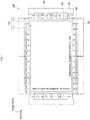
- Specifically, as illustrated in
FIG. 14A , adisplay device 10 includes a plurality ofexternal circuits 30 around aninsulating substrate 40. Flexible printedboards 50 are stacked on theinsulating substrate 40. Flexible printedboards 60 are stacked over the respective flexible printedboards 50. Theexternal circuits 30 are electrically connected to theinsulating substrate 40 via the flexible printedboards - As illustrated in
FIG. 14B , theinsulating substrate 40 includes a large number ofelectrodes 43 arranged at a predetermined pitch. Theinsulating substrate 40 further includesinsulating films 41 andinsulating films 42 that are alternately formed along the alignment direction of theelectrodes 43 so as to partially cover theelectrodes 43. - As illustrated in
FIG. 14C , the flexible printedboard 50 includes a large number ofelectrodes 51 formed at a pitch twice as large as the predetermined pitch. The flexible printedboard 60 includes a large number ofelectrodes 61 formed at a pitch twice as large as the predetermined pitch. Theelectrodes 43 exposed outside theinsulating films 42 are connected to theelectrodes 51. Theelectrodes 43 exposed inside theinsulating films 41 are connected to theelectrodes 61. - Patent Literature 1: Japanese Patent Laid-Open No.
5-196953 - In the
conventional display device 10, however, sets of the flexible printedboards electrodes 43. At this point, one ends of the flexible printedboards 50 are located on theinsulating substrate 40 while the other ends of the flexible printedboards 50 are located on theexternal circuits 30. One ends of the flexible printedboards 60 are located on theinsulating substrate 40 while the other ends of the flexible printedboards 60 are located on theexternal circuits 30. Hence, the step of mounting the flexible printed boards 50 (for example, seeFIG. 15 ) and the step of mounting the flexible printed boards 60 (for example, seeFIG. 16 ) are separately performed. Accordingly, a production lead time increases. - As illustrated in
FIG. 15 , when the flexible printedboard 50 is mounted using an anisotropic conductive film (hereinafter will be called an ACF) 53, the ACF 53 spreads like a flow. Thus, as illustrated inFIG. 16 , when the flexible printedboard 60 is mounted, theelectrodes 43 need to be spaced at intervals of about 1 mm to 2 mm in order to prevent physical interference with the spread ACF 53. The region of a frame-like terminal section is extended so as to increase in frame width. Unfortunately, the ACF 53 may prevent a reduction in frame width. - In view of the problems, an object of the present invention is to provide a display device that can prevent an increase in production lead time and an increase in the frame width of a terminal section even if the number of mounted flexible printed boards increases.
- In order to attain the object, a display device according to the present invention has the following features:
- The display device according to the present invention is defined by the subject-matter of
claim 1. - The method of manufacturing the display device according to the present invention is defined by the subject-matter of claim 6.
- According to the present invention, the one end of the first flexible printed board and the one end of the second flexible printed board are opposed to each other. Thus, the first flexible printed board and the second flexible printed board can be connected to the connecting surface of the terminal section in a single connecting step. Accordingly, even if the number of mounted flexible printed boards increases, an increase in production lead time can be avoided.
- The first protruding electrodes (the row of the first protruding electrodes) are adjacent to the second protruding electrodes (the row of the second protruding electrodes). Thus, even if the number of mounted flexible printed boards increases, an increase in the frame width of the terminal section can be avoided.
- [
FIG. 1] FIG. 1 illustrates the overall configuration of a display device according to an embodiment. - [
FIG. 2] FIG. 2 illustrates the lower right part of the display device according to the embodiment. - [
FIG. 3] FIG. 3 is a cross-sectional view of the lower right part of the display device taken along the arrows A-A' according to the embodiment. - [
FIG. 4] FIG. 4 is a cross-sectional view of the lower right part of the display device taken along the arrows B-B' according to the embodiment. - [
FIG. 5] FIG. 5 illustrates a terminal section in the display device according to the embodiment. - [
FIG. 6] FIG. 6 illustrates an arranging step in a method of manufacturing the display device according to the embodiment. - [
FIG. 7] FIG. 7 illustrates a first connecting step in the method of manufacturing the display device according to the embodiment. - [
FIG. 8] FIG. 8 illustrates a second connecting step in the method of manufacturing the display device according to the embodiment. - [
FIG. 9] FIG. 9 illustrates a folding step in the method of manufacturing the display device according to the embodiment. - [
FIG. 10] FIG. 10 illustrates a third connecting step in the method of manufacturing the display device according to the embodiment. - [
FIG. 11] FIG. 11 illustrates the vicinity of the input-side connected portion of a flexible printed board according to the embodiment. - [
FIG. 12] FIG. 12 is a cross-sectional view illustrating the vicinity of the input-side connected portion of the flexible printed board taken along the arrows C-C' according to the embodiment. - [
FIG. 13] FIG. 13 is a cross-sectional view illustrating the vertical part of a terminal section according to a modification of the embodiment. - [
FIG. 14A] FIG. 14A is a first view illustrating a connecting method of a conventional flexible printed board. - [
FIG. 14B] FIG. 14B is a second view illustrating the connecting method of the conventional flexible printed board. - [
FIG. 14C] FIG. 14C is a third view illustrating the connecting method of the conventional flexible printed board. - [
FIG. 15] FIG. 15 illustrates a first connecting step of the conventional flexible printed board. - [
FIG. 16] FIG. 16 illustrates a second connecting step of the conventional flexible printed board. - An embodiment according to the present invention will be described below with reference to the accompanying drawings.
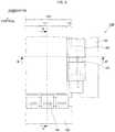
- As illustrated in
FIG. 1 , in adisplay device 100 according to the present embodiment,external circuits panel 110. Thepanel 110 includes adisplay section 111 that displays an image and aterminal section 112 formed around thedisplay section 111. Theexternal circuits panel 110 to display images on thepanel 110. - In this example, in the
display device 100, the twoexternal circuits 120 are disposed next to a horizontal part of theterminal section 112 on each of the upper and lower ends of thepanel 110 with respect to the vertical direction. Theexternal circuit 130 is disposed next to a vertical part of theterminal section 112 on each of the right and left ends of thepanel 110 with respect to the horizontal direction. The longitudinal direction of theexternal circuit 120 is aligned with the horizontal direction. The longitudinal direction of theexternal circuit 130 is aligned with the vertical direction. The longitudinal dimension of theexternal circuit 120 is substantially equal to a half of the horizontal dimension of the horizontal part of theterminal section 112. The longitudinal dimension of theexternal circuit 130 is substantially equal to the vertical dimension of the vertical part of theterminal section 112. - Moreover, in the
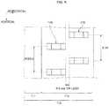
display device 100, a plurality of flexible printedboards 140 are mounted in a horizontal row on the horizontal part of theterminal section 112. A plurality of flexible printedboards 150 are mounted in a vertical row on the vertical part of theterminal section 112. Furthermore, a plurality of flexible printedboards 160 are mounted in a vertical row so as to overlap the flexible printedboards 150. As shown inFIG. 2 , theexternal circuit 120 is electrically connected to the horizontal part of theterminal section 112 via the flexible printedboards 140. Theexternal circuit 130 is electrically connected to the vertical part of theterminal section 112 via the flexible printedboards - In the
display device 100, as illustrated inFIG. 3 , a plurality of protrudingelectrodes 113 are formed in a horizontal row on the horizontal part (connecting surface) of theterminal section 112. As illustrated inFIG. 4 , a plurality of protrudingelectrodes 115 are formed in a vertical row on the vertical part (connecting surface) of theterminal section 112. Furthermore, a plurality of protrudingelectrodes 116 are formed in a vertical row on the vertical part (connecting surface) of theterminal section 112. The row of the protrudingelectrodes 115 is adjacent to the row of the protrudingelectrodes 116. The row of the protrudingelectrodes 116 is disposed between the row of the protrudingelectrodes 115 and thedisplay section 111. As illustrated inFIG. 5 , the protrudingelectrodes terminal section 112. Spacing between the row of the protrudingelectrodes 115 and the row of the protrudingelectrodes 116 is 0.5 mm or less. - In the
display device 100, as illustrated inFIG. 3 , a plurality ofmetal electrodes 121 are formed in a horizontal row on the external circuit 120 (connecting surface). As illustrated inFIG. 4 , a plurality ofmetal electrodes 131 are formed in a vertical row on the external circuit 130 (connecting surface). Furthermore, a plurality ofmetal electrodes 132 are formed in a vertical row next to themetal electrodes 131. The row of themetal electrodes 132 is located farther from theterminal section 112 than the row of themetal electrodes 131. - The
display device 100 further includes, as illustrated inFIG. 3 ,wires 145 formed only on one surface of the flexible printedboard 140. A plurality of output-side electrodes 141 and a plurality of input-side electrodes 142 are formed on the surface that bears thewires 145. Asemiconductor element 143 is mounted on the opposite side from thewires 145. Thewires 145 are connected tobumps 146 by metallic joints of gold and tin or metallic joints of gold. The output-side electrodes 141 are electrically connected to the output-side terminals of thesemiconductor element 143 via thewires 145 and thebumps 146. The input-side electrodes 142 are electrically connected to the input-side terminals of thesemiconductor element 143 via thewires 145 and thebumps 146. As shown inFIG. 4 , the flexible printedboards board 140 and thus the explanation thereof is omitted. - In the
display device 100, the surfaces of the protrudingelectrodes metal electrodes side electrodes 141 and output-side electrodes side electrodes 142 and input-side electrodes - In the
display device 100, as illustrated inFIG. 3 , the output-side electrodes 141 are disposed on one end (output-side connected portion) of the flexible printedboard 140 while the input-side electrodes 142 are disposed on the other end (input-side connected portion) of the flexible printedboard 140. The output-side electrodes 141 are connected to the protrudingelectrodes 113 covered with anACF 114. The input-side electrodes 142 are connected to themetal electrodes 121 covered with anACF 123. - In the
display device 100, as illustrated inFIG. 4 , the output-side electrodes 151 are disposed on one end (output-side connected portion) of the flexible printedboard 150 while the input-side electrodes 152 are disposed on the other end (input-side connected portion) of the flexible printedboard 150. The output-side electrode 151 is connected to the protrudingelectrode 115 in a state in which an alloy layer is formed on a contact portion between the protrudingelectrode 115 and the output-side electrode 151. The input-side electrodes 152 are connected to themetal electrodes 131 covered with anACF 133. - In the
display device 100, the output-side electrodes 161 are disposed on one end (output-side connected portion) of the flexible printedboard 160 while the input-side electrodes 162 are disposed on the other end (input-side connected portion) of the flexible printedboard 160. The output-side electrode 161 is connected to the protrudingelectrode 116 in a state in which an alloy layer is formed on a contact portion between the protrudingelectrode 116 and the output-side electrode 161. The input-side electrodes 162 are connected to themetal electrodes 132 covered with anACF 134. - In the
display device 100, the one end (output-side connected portion) of the flexible printedboard 150 and the one end (output-side connected portion) of the flexible printedboard 160 are opposed to each other. The flexible printedboard 160 is folded an even number of times between the one end (output-side connected portion) and the other end (input-side connected portion) of the flexible printedboard 160. The flexible printedboard 160 is folded to theexternal circuit 130 above theterminal section 112 so as not to block light at least to thedisplay section 111. - In the
display device 100, a control line drawn from each of the pixel portions of thedisplay section 111 to the horizontal part of theterminal section 112 is electrically connected to one of the protrudingelectrodes 113 while a control line drawn from each of the pixel portions of thedisplay section 111 to the vertical part of theterminal section 112 is electrically connected to one of the protrudingelectrodes 114 and the protrudingelectrodes 115. The pixel portions of thedisplay section 111 are driven by power and signals supplied from theexternal circuits - A method of manufacturing the
display device 100 will be described below. In this method, the flexible printedboards terminal section 112 and theexternal circuit 130. - In this manufacturing method, as illustrated in
FIG. 6 , the flexible printedboard 150 is first disposed such that the output-side electrodes 151 are located on theterminal section 112 and the input-side electrodes 152 are located on theexternal circuit 130. The flexible printedboard 160 is disposed such that the output-side electrodes 161 are located on theterminal section 112 and the input-side electrodes 162 are located on thedisplay section 111. The position of the input-side connected portion of the flexible printedboard 150 is adjusted so as to locate the input-side electrodes 152 on themetal electrodes 131. The position of the output-side connected portion of the flexible printedboard 150 is adjusted so as to locate the output-side electrodes 151 on the protrudingelectrodes 115. The position of the input-side connected portion of the flexible printedboard 160 is adjusted so as to locate the input-side electrodes 162 on themetal electrodes 132. The position of the output-side connected portion of the flexible printedboard 160 is adjusted so as to locate the output-side electrodes 161 on the protrudingelectrodes 116. - The
ACF 133 is disposed beforehand on theexternal circuit 130 so as to cover themetal electrodes 131. TheACF 133 is pressed to theexternal circuit 130 by ahead 170, which is heated to 100°C or lower, while preventing a reaction of epoxy resin in theACF 133. Similarly, theACF 134 is disposed beforehand on theexternal circuit 130 so as to cover themetal electrodes 132. TheACF 134 is pressed to theexternal circuit 130 by thehead 170, which is heated to 100°C or lower, while preventing a reaction of epoxy resin in theACF 134. - In the manufacturing method, as illustrated in
FIG. 7 , the output-side electrodes 151 of the flexible printedboard 150 are then directly connected to the protrudingelectrodes 115 of theterminal section 112; meanwhile, the output-side electrodes 161 of the flexible printedboard 160 are directly connected to the protrudingelectrodes 116 of theterminal section 112. At this point, the usedhead 170 can cover the output-side electrodes head 170 is disposed over the row of the protrudingelectrodes 115 and the row of the protrudingelectrodes 116. The output-side connected portion of the flexible printedboard 150 and the output-side connected portion of the flexible printedboard 160 are simultaneously pressed from above by thehead 170 heated to 80°C to 200°C. An ultrasonic wave with a frequency of 40 kHz to 130 kHz and an output of 2 W to 40 W is applied to thehead 170 in a state in which the output-side electrodes 151 are in contact with the protrudingelectrodes 115 and the output-side electrodes 161 are in contact with the protrudingelectrodes 116. - Thus, oxide films on the surfaces of the output-
side electrodes electrodes side electrode 151 and the protrudingelectrode 115 are rubbed against each other to form the alloy layer on the contact portion between the output-side electrode 151 and the protrudingelectrode 115; meanwhile, the newly formed surfaces of the output-side electrode 161 and the protrudingelectrode 116 are rubbed against each other to form the alloy layer on the contact portion between the output-side electrode 161 and the protrudingelectrode 116. The output-side electrodes 151 are joined to the protrudingelectrodes 115 while the output-side electrodes 161 are joined to the protrudingelectrodes 116. - In the manufacturing method, as illustrated in
FIG. 8 , the input-side electrodes 152 of the flexible printedboard 150 are then directly connected to themetal electrodes 131 of theexternal circuit 130. At this point, the input-side connected portion of the flexible printedboard 150 is pressed from above by thehead 170, which is heated to 160°C to 250°C, with a pressure of 0.5 MPa to 2 MPa for five to ten seconds. - Hence, the epoxy resin in the
ACF 133 is cured by heat in a state in which conductive particles in theACF 133 are deformed between the metal electrodes. The conductive particles can be kept in the deformed state, enabling continuity between the input-side electrodes 152 and themetal electrodes 131. - After that, in the manufacturing method, the flexible printed
board 160 is folded as illustrated inFIG. 9 . At this point, the output-side connected portion of the flexible printedboard 163 is folded such that asemiconductor element 163 mounted on the flexible printedboard 160 is located above asemiconductor element 153 mounted on the flexible printedboard 150. The input-side connected portion of the flexible printedboard 160 is folded again such that the input-side electrodes 162 of the flexible printedboard 160 are opposed to themetal electrodes 132 of theexternal circuit 130. The flexible printedboard 160 is brought closer to the flexible printedboard 150 in a state in which the flexible printedboard 160 is not in contact with the flexible printedboard 150. - In the manufacturing method, as illustrated in
FIG. 10 , the input-side electrodes 162 of the flexible printedboard 160 are then directly connected to themetal electrodes 132 of theexternal circuit 130. At this point, the input-side connected portion of the flexible printedboard 160 is pressed from above by thehead 170, which is heated to 160°C to 250°C, with a pressure of 0.5 MPa to 2 MPa for five to ten seconds. - Hence, the epoxy resin in the
ACF 134 is cured by heat in a state in which conductive particles in theACF 134 are deformed between the metal electrodes. The conductive particles can be kept in the deformed state, enabling continuity between the input-side electrodes 162 and themetal electrodes 132. - In the manufacturing method, when the input-
side electrodes 162 are connected to themetal electrodes 132, the flexible printedboard 160 is pressed in a folded state by thehead 170. At this point, a load from thehead 170 is easily released into the flexible printedboard 160 and thus the load cannot be stably applied to contact portions between the input-side electrodes 162 and themetal electrodes 132, increasing the occurrence of faulty connections. To address this problem, as illustrated inFIG. 11 , a plurality ofwires 165 on the flexible printedboard 160 are extended in parallel like straight lines along the longitudinal direction of the flexible printedboard 160. As illustrated inFIG. 12 , the flexible printedboard 160 is folded such that thewires 165 of the flexible printedboard 160 are folded above the row of themetal electrodes 132. Thus, in the third connecting step, the input-side electrodes 162 are disposed directly under thewires 165 of the flexible printedboard 160, allowing a load from thehead 170 to be evenly and stably applied to the input-side connected portion. - In the case where the flexible printed
board 140 is mounted on the horizontal part of theterminal section 112 and theexternal circuit 120, the output-side electrodes 141 are connected to the protrudingelectrodes 113 in the following steps: first, the protrudingelectrodes 113 are covered with theACF 114, and then the output-side electrodes 141 are placed on the protrudingelectrodes 113 covered with theACF 114. The output-side connected portion is then heated and pressed in a state in which the output-side electrodes 141 are placed on the protrudingelectrodes 113. Thus, the output-side electrodes 141 are connected to the protrudingelectrodes 113. The input-side electrodes 142 are connected to themetal electrodes 121 in similar steps. - According to the present embodiment, the one end (output-side connected portion) of the flexible printed
board 150 and the one end (output-side connected portion) of the flexible printedboard 160 are opposed to each other. Thus, the flexible printedboard 150 and the flexible printedboard 160 can be connected to the vertical part (connecting surface) of theterminal section 112 in a single connecting step. Accordingly, even if the number of mounted flexible printed boards increases, an increase in production lead time can be avoided. - The protruding
electrodes 115 and the protrudingelectrodes 116 are arranged in a staggered configuration. The row of the protrudingelectrodes 115 is adjacent to the row of the protrudingelectrodes 116. With this configuration, even if the number of mounted flexible printed boards increases, an increase in the frame width of theterminal section 112 can be avoided. - Specifically, the output-side connected portions of the flexible printed
boards terminal section 112 by thehead 170 pressed over the protrudingelectrodes side electrode 151 and the protrudingelectrode 115 is subjected to heat, a pressure, and an ultrasonic wave to form the alloy layer; meanwhile, the contact portion between the output-side electrode 161 and the protrudingelectrode 116 is subjected to heat, a pressure, and an ultrasonic wave to form the alloy layer. - Hence, the conventional two steps of connection can be reduced to the single step, leading to a shorter production lead time. Moreover, without using the ACF, the output-
side electrodes 151 can be directly connected to the protrudingelectrodes 115 and the output-side electrodes 161 can be directly connected to the protrudingelectrodes 116. This configuration can eliminate the need for considering an ACF flow when determining spacing between the protrudingelectrodes electrodes terminal section 112. - Unlike the structure of the flexible printed
board 140, the flexible printedboard 160 may have wires on two surfaces such that the wires on one of the surfaces are electrically connected to the wires on the other surface through vias. For example, as illustrated inFIG. 13 , the input-side electrodes 162 are formed and thesemiconductor element 163 is mounted on the opposite side from the output-side electrodes 161. In this case, the flexible printedboard 160 is folded an odd number of times between the one end (output-side connected portion) and the other end (input-side connected portion) of the flexible printedboard 160. Specifically, in the folding step, the input-side connected portion of the flexible printedboard 160 is folded such that thesemiconductor element 163 mounted on the flexible printedboard 160 is located above thesemiconductor element 153 mounted on the flexible printedboard 150 and the input-side electrodes 162 of the flexible printedboard 160 are opposed to themetal electrodes 132 of theexternal circuit 130. - The present invention can be used as a display device, for example, a liquid crystal display device and an organic EL display device which can provide high-quality display with a smaller thickness and lower power consumption.
Claims (6)
- A display device (100) comprising a panel (110) having a display section (111) that displays an image and a terminal section (112), having a horizontal edge and a vertical edge in the plane of the panel corresponding to an X and Y direction, is formed around the display section (111), wherein the display device (100) comprises a first flexible printed board (150) and a second flexible printed board (160) overlapping the first flexible printed board (150),
an external circuit (130) that controls driving of the display section (111) is disposed next to the terminal section (112) with respect to the horizontal edge of the terminal section (112), a row of first protruding electrodes (115) and a row of second protruding electrodes (116) are formed on the connecting surface of the terminal section (112),
the row of the second protruding electrodes (116) is disposed between the row of the first protruding electrodes (115) and the display section (111),
one end of the first flexible printed board (150) is connected to the row of the first protruding electrodes (115),
one end of the second flexible printed board (160) is connected to the row of the second protruding electrodes (116),
the row of the first protruding electrodes (115) is adjacent to the row of the second protruding electrodes (116),
one end face of the first flexible printed board (150) and one end face of the second flexible printed board (160) are opposed to each other, and
the second flexible printed board (160) is folded towards the external circuit (130) above the terminal section (112) so as not to block light to the display section (111). - The display device (100) according to claim 1, wherein
a row of first metal electrodes (131) and a row of second metal electrodes (132) are formed on a connecting surface of the external circuit (130),
the row of the second metal electrodes (132) is located farther from the terminal section (112) than the row of the first metal electrodes (131), the other end of the first flexible printed board (150) is connected to the row of the first metal electrodes (131), and the other end of the second flexible printed board (160) is connected to the row of the second metal electrodes (132). - The display device (100) according to claim 2, further comprising:a plurality of first electrodes (161) formed on the one end of the second flexible printed board (160), each first electrode (161) being connected to the second protruding electrode (116); anda plurality of second electrodes (162) formed on the other end of the second flexible printed board (160), each second electrode (162) being connected to one second metal electrode (132),wherein the plurality of first electrodes (161) and the plurality of second electrodes (162) are disposed on one surface of the second flexible printed board (160), andthe second flexible printed board (160) is folded an even number of times between the one end and the other end of the second flexible printed board (160).
- The display device (100) according to claim 3, wherein the second flexible printed board (160) is folded such that wires of the second flexible printed board (160) are folded above the row of the second metal electrodes (132).
- The display device (100) according to claim 2, further comprising:a plurality of first electrodes (161) formed on the end of the second flexible printed board (160), each first electrode (161) being connected to the second protruding electrode (116); anda plurality of second electrodes (162) formed on the other end of the second flexible printed board (160), each second electrode (162) being connected to the second metal electrode (132),wherein the plurality of first electrodes (161) are disposed on one of the two surfaces of the second flexible printed board (160),the plurality of second electrodes (162) are disposed on the other surface of the second flexible printed board (160), andthe second flexible printed board (160) is folded an odd number of times between the one end and the other end of the second flexible printed board (160).
- A method of manufacturing a display device (100) comprising a panel (110) having a display section (111) that displays an image and a terminal section (112) that is formed around the display section (111),
wherein a row of first protruding electrodes (115) and a row of second protruding electrodes (116) are formed on a connecting surface of the terminal section (112), the row of the second protruding electrodes (116) is disposed between the row of the first protruding electrodes (115) and the display section (111), and the row of the first protruding electrodes (115) is adjacent to the row of the second protruding electrodes (116),
the method comprising:disposing one end of a first flexible printed board (150) above the row of the first protruding electrodes (115) and disposing one end of a second flexible printed board (160) above the row of the second protruding electrodes (116) in a state in which one end face of the first flexible printed board (150) and one end face of the second flexible printed board (160) are opposed to each other, andsimultaneously pressing the one end of the first flexible printed board (150) and the one end of the second flexible printed board (160) by a head to connect the one end of the first flexible printed board (150) to the row of the first protruding electrodes (115) and the one end of the second flexible printed board (160) to the row of the second protruding electrodes (116), andfolding the second flexible printed board (160) back above the terminal section (112) so that the second flexible printed board does not block light to the display section (111) in a state in which the one end of the second flexible printed board (160) is connected to the row of the second protruding electrodes (116).
Applications Claiming Priority (2)
| Application Number | Priority Date | Filing Date | Title |
|---|---|---|---|
| JP2010141125 | 2010-06-22 | ||
| PCT/JP2011/002112WO2011161857A1 (en) | 2010-06-22 | 2011-04-11 | Display device |
Publications (3)
| Publication Number | Publication Date |
|---|---|
| EP2587471A1 EP2587471A1 (en) | 2013-05-01 |
| EP2587471A4 EP2587471A4 (en) | 2015-05-20 |
| EP2587471B1true EP2587471B1 (en) | 2018-01-10 |
Family
ID=45371065
Family Applications (1)
| Application Number | Title | Priority Date | Filing Date |
|---|---|---|---|
| EP11797747.0ANot-in-forceEP2587471B1 (en) | 2010-06-22 | 2011-04-11 | Display device |
Country Status (5)
| Country | Link |
|---|---|
| US (1) | US9042108B2 (en) |
| EP (1) | EP2587471B1 (en) |
| JP (1) | JP5719993B2 (en) |
| CN (1) | CN102834855B (en) |
| WO (1) | WO2011161857A1 (en) |
Families Citing this family (9)
| Publication number | Priority date | Publication date | Assignee | Title |
|---|---|---|---|---|
| CN103296489B (en) | 2012-04-13 | 2015-08-26 | 上海天马微电子有限公司 | Connecting device, flat panel device, image sensor, display and touch equipment |
| KR102046864B1 (en) | 2013-03-13 | 2019-11-20 | 삼성전자주식회사 | Flexible display device |
| CN103247233B (en) | 2013-04-28 | 2015-09-23 | 京东方科技集团股份有限公司 | Flexible base, board, display device and attach the method for electron device on flexible substrates |
| KR102695728B1 (en) | 2016-09-06 | 2024-08-16 | 삼성디스플레이 주식회사 | Display device |
| JP6770859B2 (en)* | 2016-09-16 | 2020-10-21 | 株式会社ジャパンディスプレイ | Display device manufacturing method |
| KR20190083014A (en)* | 2018-01-02 | 2019-07-11 | 삼성디스플레이 주식회사 | Display device |
| US10818634B2 (en)* | 2018-10-08 | 2020-10-27 | HKC Corporation Limited | Display panel, method for manufacturing the display panel, and display device |
| KR102780037B1 (en)* | 2019-04-24 | 2025-03-12 | 삼성디스플레이 주식회사 | Display apparatus assembly equipment and display apparatus assembleing method using the same |
| KR102777685B1 (en) | 2019-05-02 | 2025-03-11 | 삼성디스플레이 주식회사 | Display device |
Family Cites Families (17)
| Publication number | Priority date | Publication date | Assignee | Title |
|---|---|---|---|---|
| GB2062928B (en) | 1979-09-19 | 1983-05-25 | Sharp Kk | Electrode terminal assembly on a multilayer type liquid crystal panel |
| JPS56121018A (en)* | 1980-02-28 | 1981-09-22 | Sharp Corp | Terminal treating method for multilayer liquid-crystal panel |
| JP2908602B2 (en)* | 1991-07-01 | 1999-06-21 | 三菱電機株式会社 | Terminal connection device |
| JPH05196953A (en) | 1992-01-22 | 1993-08-06 | Fujitsu Ltd | Connecting method for wiring film |
| JPH1039775A (en)* | 1996-07-23 | 1998-02-13 | Hitachi Ltd | Liquid crystal display device |
| JP2000155306A (en) | 1998-11-19 | 2000-06-06 | Mitsubishi Electric Corp | Display device |
| JP3549760B2 (en)* | 1999-02-18 | 2004-08-04 | シャープ株式会社 | Flat panel display |
| JP3739640B2 (en)* | 2000-08-28 | 2006-01-25 | シャープ株式会社 | Manufacturing method of liquid crystal module |
| JP2002151822A (en)* | 2000-11-10 | 2002-05-24 | Seiko Epson Corp | Flexible Wiring Board Connection Structure and Connection Method, Electronic Component, and Electronic Equipment |
| US6914324B2 (en)* | 2001-10-26 | 2005-07-05 | Staktek Group L.P. | Memory expansion and chip scale stacking system and method |
| US7246431B2 (en)* | 2002-09-06 | 2007-07-24 | Tessera, Inc. | Methods of making microelectronic packages including folded substrates |
| US20040217471A1 (en)* | 2003-02-27 | 2004-11-04 | Tessera, Inc. | Component and assemblies with ends offset downwardly |
| JP4543772B2 (en)* | 2003-09-19 | 2010-09-15 | セイコーエプソン株式会社 | Electro-optical device and electronic apparatus |
| JP2005202074A (en)* | 2004-01-14 | 2005-07-28 | Mitsubishi Electric Corp | Liquid crystal display |
| JP2005241852A (en)* | 2004-02-25 | 2005-09-08 | Hitachi Displays Ltd | Display device |
| KR20080022442A (en)* | 2006-09-06 | 2008-03-11 | 삼성전자주식회사 | Flexible printed circuit board and display device having same |
| JP2009168877A (en)* | 2008-01-11 | 2009-07-30 | Seiko Epson Corp | Electro-optical device and electronic apparatus |
- 2011
- 2011-04-11EPEP11797747.0Apatent/EP2587471B1/ennot_activeNot-in-force
- 2011-04-11CNCN201180018397.1Apatent/CN102834855B/ennot_activeExpired - Fee Related
- 2011-04-11USUS13/702,216patent/US9042108B2/ennot_activeExpired - Fee Related
- 2011-04-11JPJP2012521265Apatent/JP5719993B2/enactiveActive
- 2011-04-11WOPCT/JP2011/002112patent/WO2011161857A1/enactiveApplication Filing
Non-Patent Citations (1)
| Title |
|---|
| None* |
Also Published As
| Publication number | Publication date |
|---|---|
| CN102834855B (en) | 2015-02-25 |
| WO2011161857A1 (en) | 2011-12-29 |
| US20130141881A1 (en) | 2013-06-06 |
| JP5719993B2 (en) | 2015-05-20 |
| JPWO2011161857A1 (en) | 2013-08-19 |
| EP2587471A4 (en) | 2015-05-20 |
| CN102834855A (en) | 2012-12-19 |
| US9042108B2 (en) | 2015-05-26 |
| EP2587471A1 (en) | 2013-05-01 |
Similar Documents
| Publication | Publication Date | Title |
|---|---|---|
| EP2587471B1 (en) | Display device | |
| US10076027B2 (en) | Substrate for connection and display apparatus | |
| US20070013856A1 (en) | Flexible printed circuit and display device using the same | |
| TW540256B (en) | Circuit board and method of manufacturing the same, and display apparatus | |
| US9907171B2 (en) | Flexible printed circuit boards structure | |
| US12048096B2 (en) | Printed circuit board, display module comprising the printed circuit board, display device and method of bonding the printed circuit board | |
| JP2010225845A (en) | Substrate connection structure, electro-optical device, and electronic apparatus | |
| US10264670B2 (en) | Structure for flexible printed circuit boards | |
| JP4717604B2 (en) | Wiring substrate and semiconductor device using the same | |
| WO2017138443A1 (en) | Semiconductor device and display device | |
| JP2004212587A (en) | Liquid crystal display panel and mounting method of flexible board used for liquid crystal display panel | |
| US9872389B2 (en) | Flexible printed circuit board structure | |
| CN112993607A (en) | Display device, method for manufacturing display device, and printed wiring board | |
| JP2003302914A (en) | Electronic equipment | |
| JP4575845B2 (en) | Wiring connection structure and liquid crystal display device | |
| US9899627B2 (en) | Organic light emitting diode | |
| TWI323378B (en) | Pad structure and a display substrate and a liquid crystal display device comprising the same | |
| JP4650050B2 (en) | Method for electrically installing electronic parts and method for manufacturing liquid crystal display elements | |
| US10206290B2 (en) | Method for manufacturing structure for flexible printed circuit boards | |
| JP2005121757A (en) | Substrate connection structure, electronic component, liquid crystal display device, and method of manufacturing electronic component | |
| JP2005024660A (en) | Liquid crystal display element | |
| JP2005311168A (en) | Terminal structure, and liquid crystal display element having the same | |
| TW200937598A (en) | Substrate electrode structure, and the bonding structure using the same to bond with driving element |
Legal Events
| Date | Code | Title | Description |
|---|---|---|---|
| PUAI | Public reference made under article 153(3) epc to a published international application that has entered the european phase | Free format text:ORIGINAL CODE: 0009012 | |
| 17P | Request for examination filed | Effective date:20121115 | |
| AK | Designated contracting states | Kind code of ref document:A1 Designated state(s):AL AT BE BG CH CY CZ DE DK EE ES FI FR GB GR HR HU IE IS IT LI LT LU LV MC MK MT NL NO PL PT RO RS SE SI SK SM TR | |
| DAX | Request for extension of the european patent (deleted) | ||
| RAP1 | Party data changed (applicant data changed or rights of an application transferred) | Owner name:PANASONIC INTELLECTUAL PROPERTY MANAGEMENT CO., LT | |
| RA4 | Supplementary search report drawn up and despatched (corrected) | Effective date:20150421 | |
| RIC1 | Information provided on ipc code assigned before grant | Ipc:G09F 9/00 20060101AFI20150415BHEP Ipc:G02F 1/1345 20060101ALI20150415BHEP Ipc:H01L 21/60 20060101ALI20150415BHEP | |
| GRAP | Despatch of communication of intention to grant a patent | Free format text:ORIGINAL CODE: EPIDOSNIGR1 | |
| STAA | Information on the status of an ep patent application or granted ep patent | Free format text:STATUS: GRANT OF PATENT IS INTENDED | |
| INTG | Intention to grant announced | Effective date:20170825 | |
| GRAS | Grant fee paid | Free format text:ORIGINAL CODE: EPIDOSNIGR3 | |
| GRAA | (expected) grant | Free format text:ORIGINAL CODE: 0009210 | |
| STAA | Information on the status of an ep patent application or granted ep patent | Free format text:STATUS: THE PATENT HAS BEEN GRANTED | |
| AK | Designated contracting states | Kind code of ref document:B1 Designated state(s):AL AT BE BG CH CY CZ DE DK EE ES FI FR GB GR HR HU IE IS IT LI LT LU LV MC MK MT NL NO PL PT RO RS SE SI SK SM TR | |
| REG | Reference to a national code | Ref country code:CH Ref legal event code:EP Ref country code:AT Ref legal event code:REF Ref document number:963202 Country of ref document:AT Kind code of ref document:T Effective date:20180115 | |
| REG | Reference to a national code | Ref country code:IE Ref legal event code:FG4D | |
| REG | Reference to a national code | Ref country code:DE Ref legal event code:R096 Ref document number:602011044988 Country of ref document:DE | |
| REG | Reference to a national code | Ref country code:NL Ref legal event code:MP Effective date:20180110 | |
| REG | Reference to a national code | Ref country code:AT Ref legal event code:MK05 Ref document number:963202 Country of ref document:AT Kind code of ref document:T Effective date:20180110 | |
| PG25 | Lapsed in a contracting state [announced via postgrant information from national office to epo] | Ref country code:NL Free format text:LAPSE BECAUSE OF FAILURE TO SUBMIT A TRANSLATION OF THE DESCRIPTION OR TO PAY THE FEE WITHIN THE PRESCRIBED TIME-LIMIT Effective date:20180110 | |
| PG25 | Lapsed in a contracting state [announced via postgrant information from national office to epo] | Ref country code:CY Free format text:LAPSE BECAUSE OF FAILURE TO SUBMIT A TRANSLATION OF THE DESCRIPTION OR TO PAY THE FEE WITHIN THE PRESCRIBED TIME-LIMIT Effective date:20180110 Ref country code:FI Free format text:LAPSE BECAUSE OF FAILURE TO SUBMIT A TRANSLATION OF THE DESCRIPTION OR TO PAY THE FEE WITHIN THE PRESCRIBED TIME-LIMIT Effective date:20180110 Ref country code:LT Free format text:LAPSE BECAUSE OF FAILURE TO SUBMIT A TRANSLATION OF THE DESCRIPTION OR TO PAY THE FEE WITHIN THE PRESCRIBED TIME-LIMIT Effective date:20180110 Ref country code:ES Free format text:LAPSE BECAUSE OF FAILURE TO SUBMIT A TRANSLATION OF THE DESCRIPTION OR TO PAY THE FEE WITHIN THE PRESCRIBED TIME-LIMIT Effective date:20180110 Ref country code:NO Free format text:LAPSE BECAUSE OF FAILURE TO SUBMIT A TRANSLATION OF THE DESCRIPTION OR TO PAY THE FEE WITHIN THE PRESCRIBED TIME-LIMIT Effective date:20180410 Ref country code:HR Free format text:LAPSE BECAUSE OF FAILURE TO SUBMIT A TRANSLATION OF THE DESCRIPTION OR TO PAY THE FEE WITHIN THE PRESCRIBED TIME-LIMIT Effective date:20180110 | |
| PG25 | Lapsed in a contracting state [announced via postgrant information from national office to epo] | Ref country code:RS Free format text:LAPSE BECAUSE OF FAILURE TO SUBMIT A TRANSLATION OF THE DESCRIPTION OR TO PAY THE FEE WITHIN THE PRESCRIBED TIME-LIMIT Effective date:20180110 Ref country code:PL Free format text:LAPSE BECAUSE OF FAILURE TO SUBMIT A TRANSLATION OF THE DESCRIPTION OR TO PAY THE FEE WITHIN THE PRESCRIBED TIME-LIMIT Effective date:20180110 Ref country code:BG Free format text:LAPSE BECAUSE OF FAILURE TO SUBMIT A TRANSLATION OF THE DESCRIPTION OR TO PAY THE FEE WITHIN THE PRESCRIBED TIME-LIMIT Effective date:20180410 Ref country code:AT Free format text:LAPSE BECAUSE OF FAILURE TO SUBMIT A TRANSLATION OF THE DESCRIPTION OR TO PAY THE FEE WITHIN THE PRESCRIBED TIME-LIMIT Effective date:20180110 Ref country code:IS Free format text:LAPSE BECAUSE OF FAILURE TO SUBMIT A TRANSLATION OF THE DESCRIPTION OR TO PAY THE FEE WITHIN THE PRESCRIBED TIME-LIMIT Effective date:20180510 Ref country code:GR Free format text:LAPSE BECAUSE OF FAILURE TO SUBMIT A TRANSLATION OF THE DESCRIPTION OR TO PAY THE FEE WITHIN THE PRESCRIBED TIME-LIMIT Effective date:20180411 Ref country code:LV Free format text:LAPSE BECAUSE OF FAILURE TO SUBMIT A TRANSLATION OF THE DESCRIPTION OR TO PAY THE FEE WITHIN THE PRESCRIBED TIME-LIMIT Effective date:20180110 Ref country code:SE Free format text:LAPSE BECAUSE OF FAILURE TO SUBMIT A TRANSLATION OF THE DESCRIPTION OR TO PAY THE FEE WITHIN THE PRESCRIBED TIME-LIMIT Effective date:20180110 | |
| REG | Reference to a national code | Ref country code:DE Ref legal event code:R097 Ref document number:602011044988 Country of ref document:DE | |
| PG25 | Lapsed in a contracting state [announced via postgrant information from national office to epo] | Ref country code:AL Free format text:LAPSE BECAUSE OF FAILURE TO SUBMIT A TRANSLATION OF THE DESCRIPTION OR TO PAY THE FEE WITHIN THE PRESCRIBED TIME-LIMIT Effective date:20180110 Ref country code:RO Free format text:LAPSE BECAUSE OF FAILURE TO SUBMIT A TRANSLATION OF THE DESCRIPTION OR TO PAY THE FEE WITHIN THE PRESCRIBED TIME-LIMIT Effective date:20180110 Ref country code:IT Free format text:LAPSE BECAUSE OF FAILURE TO SUBMIT A TRANSLATION OF THE DESCRIPTION OR TO PAY THE FEE WITHIN THE PRESCRIBED TIME-LIMIT Effective date:20180110 Ref country code:EE Free format text:LAPSE BECAUSE OF FAILURE TO SUBMIT A TRANSLATION OF THE DESCRIPTION OR TO PAY THE FEE WITHIN THE PRESCRIBED TIME-LIMIT Effective date:20180110 | |
| PLBE | No opposition filed within time limit | Free format text:ORIGINAL CODE: 0009261 | |
| STAA | Information on the status of an ep patent application or granted ep patent | Free format text:STATUS: NO OPPOSITION FILED WITHIN TIME LIMIT | |
| PG25 | Lapsed in a contracting state [announced via postgrant information from national office to epo] | Ref country code:SK Free format text:LAPSE BECAUSE OF FAILURE TO SUBMIT A TRANSLATION OF THE DESCRIPTION OR TO PAY THE FEE WITHIN THE PRESCRIBED TIME-LIMIT Effective date:20180110 Ref country code:SM Free format text:LAPSE BECAUSE OF FAILURE TO SUBMIT A TRANSLATION OF THE DESCRIPTION OR TO PAY THE FEE WITHIN THE PRESCRIBED TIME-LIMIT Effective date:20180110 Ref country code:DK Free format text:LAPSE BECAUSE OF FAILURE TO SUBMIT A TRANSLATION OF THE DESCRIPTION OR TO PAY THE FEE WITHIN THE PRESCRIBED TIME-LIMIT Effective date:20180110 Ref country code:MC Free format text:LAPSE BECAUSE OF FAILURE TO SUBMIT A TRANSLATION OF THE DESCRIPTION OR TO PAY THE FEE WITHIN THE PRESCRIBED TIME-LIMIT Effective date:20180110 Ref country code:CZ Free format text:LAPSE BECAUSE OF FAILURE TO SUBMIT A TRANSLATION OF THE DESCRIPTION OR TO PAY THE FEE WITHIN THE PRESCRIBED TIME-LIMIT Effective date:20180110 | |
| REG | Reference to a national code | Ref country code:CH Ref legal event code:PL | |
| 26N | No opposition filed | Effective date:20181011 | |
| REG | Reference to a national code | Ref country code:BE Ref legal event code:MM Effective date:20180430 | |
| GBPC | Gb: european patent ceased through non-payment of renewal fee | Effective date:20180411 | |
| REG | Reference to a national code | Ref country code:IE Ref legal event code:MM4A | |
| PG25 | Lapsed in a contracting state [announced via postgrant information from national office to epo] | Ref country code:LU Free format text:LAPSE BECAUSE OF NON-PAYMENT OF DUE FEES Effective date:20180411 | |
| PG25 | Lapsed in a contracting state [announced via postgrant information from national office to epo] | Ref country code:SI Free format text:LAPSE BECAUSE OF FAILURE TO SUBMIT A TRANSLATION OF THE DESCRIPTION OR TO PAY THE FEE WITHIN THE PRESCRIBED TIME-LIMIT Effective date:20180110 Ref country code:CH Free format text:LAPSE BECAUSE OF NON-PAYMENT OF DUE FEES Effective date:20180430 Ref country code:BE Free format text:LAPSE BECAUSE OF NON-PAYMENT OF DUE FEES Effective date:20180430 Ref country code:GB Free format text:LAPSE BECAUSE OF NON-PAYMENT OF DUE FEES Effective date:20180411 Ref country code:LI Free format text:LAPSE BECAUSE OF NON-PAYMENT OF DUE FEES Effective date:20180430 | |
| PG25 | Lapsed in a contracting state [announced via postgrant information from national office to epo] | Ref country code:IE Free format text:LAPSE BECAUSE OF NON-PAYMENT OF DUE FEES Effective date:20180411 Ref country code:FR Free format text:LAPSE BECAUSE OF NON-PAYMENT OF DUE FEES Effective date:20180430 | |
| PGFP | Annual fee paid to national office [announced via postgrant information from national office to epo] | Ref country code:DE Payment date:20190418 Year of fee payment:9 | |
| PG25 | Lapsed in a contracting state [announced via postgrant information from national office to epo] | Ref country code:MT Free format text:LAPSE BECAUSE OF NON-PAYMENT OF DUE FEES Effective date:20180411 | |
| PG25 | Lapsed in a contracting state [announced via postgrant information from national office to epo] | Ref country code:TR Free format text:LAPSE BECAUSE OF FAILURE TO SUBMIT A TRANSLATION OF THE DESCRIPTION OR TO PAY THE FEE WITHIN THE PRESCRIBED TIME-LIMIT Effective date:20180110 | |
| PG25 | Lapsed in a contracting state [announced via postgrant information from national office to epo] | Ref country code:PT Free format text:LAPSE BECAUSE OF FAILURE TO SUBMIT A TRANSLATION OF THE DESCRIPTION OR TO PAY THE FEE WITHIN THE PRESCRIBED TIME-LIMIT Effective date:20180110 Ref country code:HU Free format text:LAPSE BECAUSE OF FAILURE TO SUBMIT A TRANSLATION OF THE DESCRIPTION OR TO PAY THE FEE WITHIN THE PRESCRIBED TIME-LIMIT; INVALID AB INITIO Effective date:20110411 | |
| PG25 | Lapsed in a contracting state [announced via postgrant information from national office to epo] | Ref country code:MK Free format text:LAPSE BECAUSE OF NON-PAYMENT OF DUE FEES Effective date:20180110 | |
| REG | Reference to a national code | Ref country code:DE Ref legal event code:R119 Ref document number:602011044988 Country of ref document:DE | |
| PG25 | Lapsed in a contracting state [announced via postgrant information from national office to epo] | Ref country code:DE Free format text:LAPSE BECAUSE OF NON-PAYMENT OF DUE FEES Effective date:20201103 |