EP2577477B1 - Integration of processor and input/output hub - Google Patents
Integration of processor and input/output hubDownload PDFInfo
- Publication number
- EP2577477B1 EP2577477B1EP11790212.2AEP11790212AEP2577477B1EP 2577477 B1EP2577477 B1EP 2577477B1EP 11790212 AEP11790212 AEP 11790212AEP 2577477 B1EP2577477 B1EP 2577477B1
- Authority
- EP
- European Patent Office
- Prior art keywords
- processor
- logic
- iio
- signal
- sideband
- Prior art date
- Legal status (The legal status is an assumption and is not a legal conclusion. Google has not performed a legal analysis and makes no representation as to the accuracy of the status listed.)
- Active
Links
Images


Classifications
- G—PHYSICS
- G06—COMPUTING OR CALCULATING; COUNTING
- G06F—ELECTRIC DIGITAL DATA PROCESSING
- G06F1/00—Details not covered by groups G06F3/00 - G06F13/00 and G06F21/00
- G06F1/26—Power supply means, e.g. regulation thereof
- G06F1/32—Means for saving power
- G06F1/3203—Power management, i.e. event-based initiation of a power-saving mode
- G06F1/3234—Power saving characterised by the action undertaken
- G06F1/3243—Power saving in microcontroller unit
- G—PHYSICS
- G06—COMPUTING OR CALCULATING; COUNTING
- G06F—ELECTRIC DIGITAL DATA PROCESSING
- G06F1/00—Details not covered by groups G06F3/00 - G06F13/00 and G06F21/00
- G06F1/26—Power supply means, e.g. regulation thereof
- G06F1/32—Means for saving power
- G06F1/3203—Power management, i.e. event-based initiation of a power-saving mode
- G06F1/3206—Monitoring of events, devices or parameters that trigger a change in power modality
- G—PHYSICS
- G06—COMPUTING OR CALCULATING; COUNTING
- G06F—ELECTRIC DIGITAL DATA PROCESSING
- G06F1/00—Details not covered by groups G06F3/00 - G06F13/00 and G06F21/00
- G06F1/26—Power supply means, e.g. regulation thereof
- G06F1/32—Means for saving power
- G06F1/3203—Power management, i.e. event-based initiation of a power-saving mode
- G06F1/3234—Power saving characterised by the action undertaken
- G06F1/324—Power saving characterised by the action undertaken by lowering clock frequency
- G—PHYSICS
- G06—COMPUTING OR CALCULATING; COUNTING
- G06F—ELECTRIC DIGITAL DATA PROCESSING
- G06F1/00—Details not covered by groups G06F3/00 - G06F13/00 and G06F21/00
- G06F1/26—Power supply means, e.g. regulation thereof
- G06F1/32—Means for saving power
- G06F1/3203—Power management, i.e. event-based initiation of a power-saving mode
- G06F1/3234—Power saving characterised by the action undertaken
- G06F1/3287—Power saving characterised by the action undertaken by switching off individual functional units in the computer system
- Y—GENERAL TAGGING OF NEW TECHNOLOGICAL DEVELOPMENTS; GENERAL TAGGING OF CROSS-SECTIONAL TECHNOLOGIES SPANNING OVER SEVERAL SECTIONS OF THE IPC; TECHNICAL SUBJECTS COVERED BY FORMER USPC CROSS-REFERENCE ART COLLECTIONS [XRACs] AND DIGESTS
- Y02—TECHNOLOGIES OR APPLICATIONS FOR MITIGATION OR ADAPTATION AGAINST CLIMATE CHANGE
- Y02D—CLIMATE CHANGE MITIGATION TECHNOLOGIES IN INFORMATION AND COMMUNICATION TECHNOLOGIES [ICT], I.E. INFORMATION AND COMMUNICATION TECHNOLOGIES AIMING AT THE REDUCTION OF THEIR OWN ENERGY USE
- Y02D10/00—Energy efficient computing, e.g. low power processors, power management or thermal management
Definitions
- the present disclosuregenerally relates to the field of electronics. More particularly, an embodiment of the invention relates to techniques for integration of a processor and an Input/Output (I/O) hub.
- I/OInput/Output
- a processormay communicate with input/output (I/O) devices via an I/O Hub (IOH). Furthermore, the processor may be provided on a different integrated circuit (IC) device than the IOH. A bus may be used to communicate between these IC devices.
- IOHinput/output
- ICintegrated circuit
- Such implementationsmay, however, reduce speed, e.g., due to delay associated with communicating signals between the IC devices, and/or increase power consumption, e.g., due to presence of additional circuitry required to allow for communication between the IC devices. Also, additional (board) space may be required for the discrete IOH component(s).
- US 2008/062927discloses a processor with a plurality of multithreaded processor cores with a messaging network connected to the processor cores and a plurality of communication ports.
- the messaging networkmay connect to a bus such as a PCI express interface to provide high-bandwidth communications between computer systems and memory.
- US 2010/083026discloses a first integrated circuit coupled to a second integrated circuit by a communications interface and an inter-processor communication channel between the first and second integrated circuits so that the second integrated circuit may send an advisory signal via the channel to the first integrated circuit.
- the advisory signalmay be transmitted by a sideband of the IPC channel.
- US 6,442,697discloses an integrated circuit comprising a CPU and a PLL coupled to the CPU in which the PLL is configured to allow the CPU to operate in more than one power consumption state.
- Some embodimentsrelate to techniques to reduce delay, reduce power consumption, reduce die size, and/or reduce complexity associated with power management in a computing device.
- some embodimentsallow for more control and/or communication bandwidth between the two integrated components, e.g., to further refine power state manipulation/control.
- an IOHmay be integrated on the same IC device as a processor (which may include one or more processor cores as discussed herein in more detail below). This allows for removal of logic that is only needed for off-chip communication. For example, logic associated with transmission of signals off chip across an interconnect (e.g., physical link) may be removed. Also, logic that would normally control transmitting, training, testing, power state management, etc. of the physical link may be removed.
- a processorwhich may include one or more processor cores as discussed herein in more detail below.
- the same communication mechanismsmay be maintained in some embodiments, e.g., to allow for compatibility with other existing logic, communication protocols, design requirements, etc.
- the QPI physical layer and lower link layermay be removed.
- the physical layermay be.
- one or more of the followingmay be utilized to provide the integrated IOH (110) and processor:
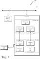
- FIG. 1illustrates a block diagram of portions of a computing system 100, according to an embodiment.
- the system 100may include a Central Processing Unit (CPU) 101 (or more generally a processor) which includes a processor portion 102.
- CPU 101 componentsmay be on a single IC die.
- the CPU 101may include one or more processors (or processor cores) as discussed herein, e.g., with reference to Fig. 5 .
- the processor 102may include various components, such as private or shared cache(s), execution unit(s), one or more memory/graphics control modules, etc. (not shown).
- the CPU 101may communicate through a bus 104 with other components such as a system memory 106.
- the memory 106may store data at the direction of the CPU 101, e.g., communicated with one or more I/O devices 107.
- the device(s) 107may be a peripheral device that communicates in accordance with the Peripheral Component Interconnect (PCI) (and its variations such as PCI express (PCIe) specification, Revision 2.0, 2006) (and/or other proprietary or non-proprietary I/O interconnect(s) such as Direct Memory Interface (DMI)) in some embodiments.
- PCIPeripheral Component Interconnect
- PCIePCI express
- DMIDirect Memory Interface
- the CPU 101may include an 110 120 that provides support for communicating with the device(s) 107 in accordance with the aforementioned PCIe specification and/or DMI.
- the processor 102may include a protocol logic 108 (e.g., to provide the support for shutting down or waking system 100), an upper link layer logic 110 (e.g., to provide link support for upper link layer communication with the 110 120), and a sideband control logic 112 (e.g., to provide sideband communication support in lieu of removal of the QPI physical layer and lower link layer, as discussed above).
- the upper link layer logicmay include one or more of: virtual channel queue(s), flow control and/or credits logic, CRC (Cyclical Redundancy Check) check and/or generation logic, parameter exchange logic, etc.
- the removed lower link layersmay include Phit/Flit assembly/deassembly/swizzling, physical layer control registers, link power (e.g., L0s) and width modes, link initialization/training, etc.
- the 110 120may include a sideband control logic 124 (e.g., to communicate sideband signals with the logic 112), one or more FIFOs 126 (e.g., to enable deterministic data transfer between the upper link layer 110 and 110 120 via an interconnect/bus 127), a link logic 128 (e.g., to provide link support for communication between the processor 102 and the 110 120), and a protocol logic 130 (e.g., to provide the support for shutting down or waking system 100).
- a sideband control logic 124e.g., to communicate sideband signals with the logic 112
- one or more FIFOs 126e.g., to enable deterministic data transfer between the upper link layer 110 and 110 120 via an interconnect/bus 127
- a link logic 128e.g., to provide link support for communication between the processor 102 and the 110 120
- a protocol logic 130e.g., to provide the support for shutting down or waking system 100.
- a relatively wider and/or slower bus/interconnect 127may eliminate high speed circuit and power challenges (when compared with the bus/interconnect that couples the non-integrated processor and IOH, for example).
- the bus 127is widened four times, allowing the frequency to be reduced by four times. A valid bit may be added to allow for more flexibility (null flits are now optional, etc.) and/or to support tester modes.
- FIFOs 126going in both directions (to and from 110 120) are added.
- the datais written into a FIFO based on a write pointer and is read by the receiver based on a read pointer.
- the separation of the write and read pointersmay be programmable, for example, to account for clock skew differences between the processor 102 components (e.g., logic 110) and 110 120. This allows the processor 102 and IIO 120 to run off of different Phase-Locked Loops (PLLs) for flexibility, finer granularity of power states, etc.
- PLLsPhase-Locked Loops
- sideband signalsare used (e.g., via logics 112 and 124):
- Figs. 2-3illustrate signals/messages exchanged between the processor 102 and IIO 120, according to some embodiments.
- Fig. 2illustrates entry into a low power state (e.g., C6/C7).
- Fig. 3illustrates entry into a medium low power state (e.g., C3) that is not as low as the case shown in Fig. 2 (e.g., with a faster wake time, for example).
- Figs. 2-3illustrate an example with "0" indicating "not” and "1” indicating "yes"
- various embodimentsmay be implemented by using other types of symbols, reverse 0/1, etc.
- one or more handshakesare performed including a Power Management Request (PMREQ) transmitted from the processor 102; the IIO 120 responds with an Completed (CMPD) signal; the processor 102 requests entry into L1 state; and the IIO 120 acknowledges the L1 request.
- PMREQPower Management Request
- CMPDCompleted
- sideband signalsare transmitted as shown.
- the processormay unlock its PLL(s) between processor_is_awake and processor_wake.
- IIOmay have a lock out window between IIO_wake and processor_is_awake (e.g., to not initiate a wake to prevent unwanted corner cases). Further, between processor_wake and IIO_is_awake, the IIO unlocks its PLL(s).
- FIG. 3Similar handshakes may be performed in the exchange of Fig. 3 .
- the processor_wake and IIO_is_awake signalare not transmitted when compared with the case in Fig. 2 .
- the protocolsupports either processor transmitting processor_is_awake or the IIO asserting IIO_wake to initiate the wake in an embodiment.
- the same mechanismmay handle early wake events that occur before the processor/IIO have fully powered down.
- Fig. 3shows an example where the processor initiates the wake before the processor/IIO has gone into the deepest power state.
- IIO or processormay initiate a wake from low power state (e.g., without QPI messages). This was previously done over QPI with analog levels and level detectors.
- IIOinitiates a wake by asserting IIO_wake.
- Processormay initiate a wake by asserting processor_wake. Once the wake signal is transmitted, the remaining signals may be sent in a specific order to complete the wake.
- the protocol(marked with *) also supports the IIO already being awake during the low power state (another medium low power state). In that case, IIO_is_awake may already have been asserted by this point.
- optional sideband signalsare used for more granularity/control power modes between the IIO and processor such as one or more of the following:
- additional signalsmay also be used to take advantage of common mechanisms (more space/power reductions).
- common infrastructure features present on chipsmay be combined for additional reduction such as:
- the IIOresets the processor the same way that the IOH reset the discrete processor. Further, the circuits to drive the pin may be removed for power/space reduction.
- Fig. 4illustrates a block diagram of a computing system 400, according to an embodiment of the invention.
- the system 400may include one or more agents 402-1 through 402-M (collectively referred to herein as “agents 402" or more generally “agent 402").
- agents 402may be any of components of a computing system, such as the computing systems discussed with reference to Figs. 1 or 5 .
- the agents 402may communicate via a network fabric 404.
- the network fabric 404may include a computer network that allows various agents (such as computing devices) to communicate data.
- the network fabric 404may include one or more interconnects (or interconnection networks) that communicate via a serial (e.g., point-to-point) link and/or a shared communication network.
- some embodimentsmay facilitate component debug or validation on links that allow communication with fully buffered dual in-line memory modules (FBD), e.g., where the FBD link is a serial link for coupling memory modules to a host controller device (such as a processor or memory hub).
- Debug informationmay be transmitted from the FBD channel host such that the debug information may be observed along the channel by channel traffic trace capture tools (such as one or more logic analyzers).
- the system 400may support a layered protocol scheme, which may include a physical layer, a link layer, a routing layer, a transport layer, and/or a protocol layer.
- the fabric 404may further facilitate transmission of data (e.g., in form of packets) from one protocol (e.g., caching processor or caching aware memory controller) to another protocol for a point-to-point or shared network.
- the network fabric 404may provide communication that adheres to one or more cache coherent protocols.
- the agents 402may transmit and/or receive data via the network fabric 404.
- some agentsmay utilize a unidirectional link while others may utilize a bidirectional link for communication.
- one or more agentssuch as agent 402-M
- may transmit datae.g., via a unidirectional link 406
- other agent(s)such as agent 402-2
- may receive datae.g., via a unidirectional link 408
- some agent(s)such as agent 402-1
- may both transmit and receive datae.g., via a bidirectional link 410.
- Fig. 5illustrates a computing system 500 that is arranged in a point-to-point (PtP) configuration, according to an embodiment of the invention.
- Fig. 5shows a system where processors, memory, and input/output devices are interconnected by a number of point-to-point interfaces.
- the operations discussed with reference to Figs. 1-4may be performed by one or more components of the system 500.
- the system 500may include several processors, of which only two, processors 502 and 504 are shown for clarity.
- the processors 502 and 504may each include a local memory controller hub (MCH) 506 and 508 to enable communication with memories 510 and 512.
- the memories 510 and/or 512may store various data such as those discussed with reference to the memory 106 of Fig. 1 .
- the processors 502 and 504may also include IIO logic 120 such as those discussed with reference to Figs. 1-4 .
- IIO logic 120such as those discussed with reference to Figs. 1-4 .
- some embodimentsmay utilize a single IIO logic 120.
- Fig. 5illustrates each IIO logic 120 coupled to one I/O device or I/O device type, each IIO logic 120 may be coupled to more than one or more than one type of I/O devices.
- the processors 502 and 504may be one of the processors 502 discussed with reference to Fig. 5 .
- the processors 502 and 504may exchange data via a point-to-point (PtP) interface 514 using PtP interface circuits 516 and 518, respectively.
- PtPpoint-to-point
- one or more of the processors 502 and 504may exchange data with a chipset 520 via individual PtP interfaces (e.g., interface 524) using point-to-point interface circuits 526, 528, and 532.
- only one processormay communicate with the chipset 520.
- a processore.g., processor 504 may exchange data with a high-performance graphics circuit 534.
- the I/O functionalitymay be integrated into the processors 502/504.
- Other embodiments of the inventionmay exist in other circuits, logic units, or devices within the system 500 of Fig. 5 .
- other embodiments of the inventionmay be distributed throughout several circuits, logic units, or devices illustrated in Fig. 5 .
- the chipset 520may communicate with a bus 540 (e.g., using an interface circuit 541).
- the bus 540may have one or more devices that communicate with it, such as a bus bridge 542 and I/O devices 543 (which may communicate with the IIO via other components such as shown in Fig. 5 or directly as shown in Fig. 1 , for example).
- the bus bridge 542may communicate with other devices such as a keyboard/mouse 545, communication devices 546 (such as modems, network interface devices, or other communication devices that may communicate with the computer network 405), audio I/O device, and/or a data storage device 548.
- the data storage device 548may store code 549 that may be executed by the processors 502 and/or 504.
- Figs. 6-7illustrate signals/messages exchanged between a processor and IIO logic, according to some embodiments.
- Fig. 6illustrates processor initiated wake to accommodate a PECI (Platform Environmental Control Interface, e.g., for processor thermal management) based wake event/request which ramps the power for IIO logic without fully waking the IIO logic (e.g., while power is applied to the IIO, the clocks/PLLs remain off).
- PECIrefers to a sideband interface to a processor which is used to manage a processor's thermal controls/operations. It reflects one mechanism that allows waking of a processor. It provides a wake event that does not involve I/O, so it does necessitate the use of the IIO.
- FIG. 7illustrates a processor initiated sleep after a wake due to PECI request such as shown in Fig. 6 .
- Figs. 6-7illustrate an example with "0" indicating “not” and “1” indicating “yes”
- various embodimentsmay be implemented by using other types of symbols, reverse 0/1, etc.
- the operations discussed hereinmay be implemented as hardware (e.g., circuitry), software, firmware, microcode, or combinations thereof, which may be provided as a computer program product, e.g., including a machine-readable or computer-readable storage medium having stored thereon instructions (or software procedures) used to program a computer to perform a process discussed herein.
- the storage mediummay include volatile and/or nonvolatile memory (or storage).
- nonvolatile memorymay include one or more of the following: read-only memory (ROM), programmable ROM (PROM), erasable PROM (EPROM), electrically EPROM (EEPROM), a disk drive (e.g., 528), a floppy disk, a compact disk ROM (CD-ROM), a digital versatile disk (DVD), flash memory, a magneto-optical disk, or other types of nonvolatile machine-readable media capable of storing electronic data (e.g., including instructions).
- Volatile memorymay include devices such as random access memory (RAM), dynamic RAM (DRAM), synchronous DRAM (SDRAM), static RAM (SRAM), etc.
- the term "logic"may include, by way of example, software, hardware, or combinations of software and hardware.
- the machine-readable mediummay include a storage device such as those discussed herein. Additionally, such computer-readable media may be downloaded as a computer program product, wherein the program may be transferred from a remote computer (e.g., a server) to a requesting computer (e.g., a client) through data signals provided in a propagation medium via a communication link (e.g., a bus, a modem, or a network connection).
- a remote computere.g., a server
- a requesting computere.g., a client
- a communication linke.g., a bus, a modem, or a network connection
- Coupledmay mean that two or more elements are in direct physical or electrical contact.
- Coupledmay mean that two or more elements are in direct physical or electrical contact.
- coupledmay also mean that two or more elements may not be in direct contact with each other, but may still cooperate or interact with each other.
Landscapes
- Engineering & Computer Science (AREA)
- Theoretical Computer Science (AREA)
- General Engineering & Computer Science (AREA)
- Physics & Mathematics (AREA)
- General Physics & Mathematics (AREA)
- Computer Hardware Design (AREA)
- Computing Systems (AREA)
- Power Sources (AREA)
- Logic Circuits (AREA)
Description
- The present disclosure generally relates to the field of electronics. More particularly, an embodiment of the invention relates to techniques for integration of a processor and an Input/Output (I/O) hub.
- In some current implementations, a processor may communicate with input/output (I/O) devices via an I/O Hub (IOH). Furthermore, the processor may be provided on a different integrated circuit (IC) device than the IOH. A bus may be used to communicate between these IC devices.
- Such implementations may, however, reduce speed, e.g., due to delay associated with communicating signals between the IC devices, and/or increase power consumption, e.g., due to presence of additional circuitry required to allow for communication between the IC devices. Also, additional (board) space may be required for the discrete IOH component(s).
US 2008/062927 discloses a processor with a plurality of multithreaded processor cores with a messaging network connected to the processor cores and a plurality of communication ports. The messaging network may connect to a bus such as a PCI express interface to provide high-bandwidth communications between computer systems and memory.US 2010/083026 discloses a first integrated circuit coupled to a second integrated circuit by a communications interface and an inter-processor communication channel between the first and second integrated circuits so that the second integrated circuit may send an advisory signal via the channel to the first integrated circuit. The advisory signal may be transmitted by a sideband of the IPC channel.US 6,442,697 discloses an integrated circuit comprising a CPU and a PLL coupled to the CPU in which the PLL is configured to allow the CPU to operate in more than one power consumption state.- The detailed description is provided with reference to the accompanying figures. In the figures, the left-most digit(s) of a reference number identifies the figure in which the reference number first appears. The use of the same reference numbers in different figures indicates similar or identical items.
FIGS. 1 and4-5 illustrate block diagrams of embodiments of computing systems, which may be utilized to implement various embodiments discussed herein.FIGS. 2-3 and6-7 illustrate signals or messages exchanged between portions of a processor, according to some embodiments.- In the following description, numerous specific details are set forth in order to provide a thorough understanding of various embodiments. However, some embodiments may be practiced without the specific details. In other instances, well-known methods, procedures, components, and circuits have not been described in detail so as not to obscure the particular embodiments.
- Some embodiments relate to techniques to reduce delay, reduce power consumption, reduce die size, and/or reduce complexity associated with power management in a computing device. In addition, some embodiments allow for more control and/or communication bandwidth between the two integrated components, e.g., to further refine power state manipulation/control.
- In an embodiment, an IOH may be integrated on the same IC device as a processor (which may include one or more processor cores as discussed herein in more detail below). This allows for removal of logic that is only needed for off-chip communication. For example, logic associated with transmission of signals off chip across an interconnect (e.g., physical link) may be removed. Also, logic that would normally control transmitting, training, testing, power state management, etc. of the physical link may be removed.
- Even though the physical link and additional logic is removed, the same communication mechanisms may be maintained in some embodiments, e.g., to allow for compatibility with other existing logic, communication protocols, design requirements, etc. For instance, in a QPI (Quick Path Interconnect) based processor, the QPI physical layer and lower link layer may be removed. For the accompanying IOH, the physical layer may be.
- In some embodiments, one or more of the following may be utilized to provide the integrated IOH (110) and processor:
- 1. a wider and/or slower bus/interconnect to couple the processor components and 110, e.g., to eliminate high speed circuit and power challenges (when compared with the bus/interconnect that couples the non-integrated processor and IOH, for example);
- 2. one or more First-In, First-Out (FIFO) devices to enable deterministic data transfer between the processor and Integrated IIO;
- 3. one or more side band signals to signal powering up and down of the link(s) between the processor and IIO;
- 4. protocol to enable either side to initiate shutting down or waking up of the computing system that includes the processor;
- 5. optional side band signals to further control granularity/depth of low power states; and/or
- 6. additional signal(s) to take advantage of common mechanisms (e.g., for more space/power reductions).
- One or more of the above-mentioned elements may be provided in various computing environments. More particularly,
Fig. 1 illustrates a block diagram of portions of acomputing system 100, according to an embodiment. - The
system 100 may include a Central Processing Unit (CPU) 101 (or more generally a processor) which includes aprocessor portion 102.CPU 101 components may be on a single IC die. TheCPU 101 may include one or more processors (or processor cores) as discussed herein, e.g., with reference toFig. 5 . Theprocessor 102 may include various components, such as private or shared cache(s), execution unit(s), one or more memory/graphics control modules, etc. (not shown). Moreover, theCPU 101 may communicate through abus 104 with other components such as asystem memory 106. Thememory 106 may store data at the direction of theCPU 101, e.g., communicated with one or more I/O devices 107. The device(s) 107 may be a peripheral device that communicates in accordance with the Peripheral Component Interconnect (PCI) (and its variations such as PCI express (PCIe) specification, Revision 2.0, 2006) (and/or other proprietary or non-proprietary I/O interconnect(s) such as Direct Memory Interface (DMI)) in some embodiments. As will be further discussed below, theCPU 101 may include an 110 120 that provides support for communicating with the device(s) 107 in accordance with the aforementioned PCIe specification and/or DMI. - As illustrated in
Fig. 1 , theprocessor 102 may include a protocol logic 108 (e.g., to provide the support for shutting down or waking system 100), an upper link layer logic 110 (e.g., to provide link support for upper link layer communication with the 110 120), and a sideband control logic 112 (e.g., to provide sideband communication support in lieu of removal of the QPI physical layer and lower link layer, as discussed above). In an embodiment, the upper link layer logic may include one or more of: virtual channel queue(s), flow control and/or credits logic, CRC (Cyclical Redundancy Check) check and/or generation logic, parameter exchange logic, etc. Furthermore, the removed lower link layers, in accordance with some embodiments, may include Phit/Flit assembly/deassembly/swizzling, physical layer control registers, link power (e.g., L0s) and width modes, link initialization/training, etc. - The 110 120 may include a sideband control logic 124 (e.g., to communicate sideband signals with the logic 112), one or more FIFOs 126 (e.g., to enable deterministic data transfer between the
upper link layer processor 102 and the 110 120), and a protocol logic 130 (e.g., to provide the support for shutting down or waking system 100). - In an embodiment, a relatively wider and/or slower bus/
interconnect 127 may eliminate high speed circuit and power challenges (when compared with the bus/interconnect that couples the non-integrated processor and IOH, for example). In one embodiment, thebus 127 is widened four times, allowing the frequency to be reduced by four times. A valid bit may be added to allow for more flexibility (null flits are now optional, etc.) and/or to support tester modes. - In some embodiments, FIFOs 126 going in both directions (to and from 110 120) are added. When transferring data between the
processor 102 components (e.g., logic 110) and 110 120, the data is written into a FIFO based on a write pointer and is read by the receiver based on a read pointer. The separation of the write and read pointers may be programmable, for example, to account for clock skew differences between theprocessor 102 components (e.g., logic 110) and 110 120. This allows theprocessor 102 andIIO 120 to run off of different Phase-Locked Loops (PLLs) for flexibility, finer granularity of power states, etc. - In an embodiment, the following sideband signals are used (e.g., via
logics 112 and 124): - 1. From the 110 120:
- A. IIO_wake -
IIO 120 requests to wakesystem 100 that is in low power mode; and - B. IIO_is_awake -
IIO 120 is awake and may function (for instance, power is ramped, PLL's locked, etc.); and
- A. IIO_wake -
- 2. From the processor 102:
- A. processor_wake (e.g., WAKEUP_IIO_PLL)-
processor 102 request to wakesystem 100 that is in low power mode; and - B. processor_is_awake (e.g., BGFRun)-
processor 102 is awake. In some embodiments, this signal may also indicate both theprocessor 102 andIIO 120 are awake. In turn, theprocessor 102 may determine when thewhole CPU 101 chip is up and ready to run based on the IIO_is _awake signal. This signal may reset the FIFO pointers and allows the FIFO(s) 126 it to transfer data.
- A. processor_wake (e.g., WAKEUP_IIO_PLL)-
Figs. 2-3 illustrate signals/messages exchanged between theprocessor 102 andIIO 120, according to some embodiments.Fig. 2 illustrates entry into a low power state (e.g., C6/C7).Fig. 3 illustrates entry into a medium low power state (e.g., C3) that is not as low as the case shown inFig. 2 (e.g., with a faster wake time, for example). Moreover, even thoughFigs. 2-3 illustrate an example with "0" indicating "not" and "1" indicating "yes", various embodiments may be implemented by using other types of symbols, reverse 0/1, etc.- As shown in
Fig. 2 , one or more handshakes (e.g., in accordance with QPI) are performed including a Power Management Request (PMREQ) transmitted from theprocessor 102; theIIO 120 responds with an Completed (CMPD) signal; theprocessor 102 requests entry into L1 state; and theIIO 120 acknowledges the L1 request. After the handshakes, sideband signals are transmitted as shown. As shown, the processor may unlock its PLL(s) between processor_is_awake and processor_wake. Also, IIO may have a lock out window between IIO_wake and processor_is_awake (e.g., to not initiate a wake to prevent unwanted corner cases). Further, between processor_wake and IIO_is_awake, the IIO unlocks its PLL(s). - Similar handshakes may be performed in the exchange of
Fig. 3 . The processor_wake and IIO_is_awake signal are not transmitted when compared with the case inFig. 2 . To wake from the medium low power state, the protocol supports either processor transmitting processor_is_awake or the IIO asserting IIO_wake to initiate the wake in an embodiment. The same mechanism may handle early wake events that occur before the processor/IIO have fully powered down. For example,Fig. 3 shows an example where the processor initiates the wake before the processor/IIO has gone into the deepest power state. - Furthermore, the IIO or processor may initiate a wake from low power state (e.g., without QPI messages). This was previously done over QPI with analog levels and level detectors. In an embodiment, IIO initiates a wake by asserting IIO_wake. Processor may initiate a wake by asserting processor_wake. Once the wake signal is transmitted, the remaining signals may be sent in a specific order to complete the wake.
- For example, for an IIO initiated wake, the following sequence occurs (which assumes that signals are normally high - but of course the reverse implementation is also contemplated in some embodiments):
- IIO_wake 0->1
- processor_wake 0->1
- IIO_is_awake 0->1 (*)
- processor_is_awake 0->1
- The protocol (marked with *) also supports the IIO already being awake during the low power state (another medium low power state). In that case, IIO_is_awake may already have been asserted by this point.
- In some embodiments, optional sideband signals are used for more granularity/control power modes between the IIO and processor such as one or more of the following:
- 1. From the processor:
- A. ForcePwrRamp (PCUtoIIOForceRmp)- processor requests IIO to turn on or off its power. This may be useful for modes where processor is to wake but knows the IIO will not be fully woken. Rather than go through the full protocol, only the power needs to be turned on to enable using repeaters, etc. in the IIO for processor purposes.
- 2. From the IIO:
- A. PwrGood (IIOtoPCUPwrGd) - IIO indicates power is sufficient within the IIO and the processor ForcePwrRamp is asserted.
- In various embodiments, additional signals may also be used to take advantage of common mechanisms (more space/power reductions). For instance, common infrastructure features present on chips may be combined for additional reduction such as:
- (1) Fuses - Separate fuse blocks with a number of common fuses are not needed anymore. A single fuse block, e.g., with additional fuse(s) added for unique IIO fused options may be used. The interface may be a serial download fuse bus to the IIO, e.g., which may be identical to the fuse bus that is coupled to the rest of the processor blocks.
- (2) Frequency selection - Non-integrated components generally require separate mechanisms to select the frequency of key interfaces. This selection mechanism requires power cycle reset and careful coordination between the two components. With the integrated IIO and processor, one frequency selection logic may be removed and both the IIO and processor frequency selected off of a single frequency selection logic. This may be done with sideband signals that reflect the clock ratio.
- In an embodiment, the IIO resets the processor the same way that the IOH reset the discrete processor. Further, the circuits to drive the pin may be removed for power/space reduction.
Fig. 4 illustrates a block diagram of a computing system 400, according to an embodiment of the invention. The system 400 may include one or more agents 402-1 through 402-M (collectively referred to herein as "agents 402" or more generally "agent 402"). In an embodiment, one or more of theagents 402 may be any of components of a computing system, such as the computing systems discussed with reference toFigs. 1 or5 .- As illustrated in
Fig. 4 , theagents 402 may communicate via anetwork fabric 404. In one embodiment, thenetwork fabric 404 may include a computer network that allows various agents (such as computing devices) to communicate data. In an embodiment, thenetwork fabric 404 may include one or more interconnects (or interconnection networks) that communicate via a serial (e.g., point-to-point) link and/or a shared communication network. For example, some embodiments may facilitate component debug or validation on links that allow communication with fully buffered dual in-line memory modules (FBD), e.g., where the FBD link is a serial link for coupling memory modules to a host controller device (such as a processor or memory hub). Debug information may be transmitted from the FBD channel host such that the debug information may be observed along the channel by channel traffic trace capture tools (such as one or more logic analyzers). - In one embodiment, the system 400 may support a layered protocol scheme, which may include a physical layer, a link layer, a routing layer, a transport layer, and/or a protocol layer. The
fabric 404 may further facilitate transmission of data (e.g., in form of packets) from one protocol (e.g., caching processor or caching aware memory controller) to another protocol for a point-to-point or shared network. Also, in some embodiments, thenetwork fabric 404 may provide communication that adheres to one or more cache coherent protocols. - Furthermore, as shown by the direction of arrows in
Fig. 4 , theagents 402 may transmit and/or receive data via thenetwork fabric 404. Hence, some agents may utilize a unidirectional link while others may utilize a bidirectional link for communication. For instance, one or more agents (such as agent 402-M) may transmit data (e.g., via a unidirectional link 406), other agent(s) (such as agent 402-2) may receive data (e.g., via a unidirectional link 408), while some agent(s) (such as agent 402-1) may both transmit and receive data (e.g., via a bidirectional link 410). Fig. 5 illustrates acomputing system 500 that is arranged in a point-to-point (PtP) configuration, according to an embodiment of the invention. In particular,Fig. 5 shows a system where processors, memory, and input/output devices are interconnected by a number of point-to-point interfaces. The operations discussed with reference toFigs. 1-4 may be performed by one or more components of thesystem 500.- As illustrated in
Fig. 5 , thesystem 500 may include several processors, of which only two,processors processors memories memories 510 and/or 512 may store various data such as those discussed with reference to thememory 106 ofFig. 1 . As shown inFig. 5 , theprocessors IIO logic 120 such as those discussed with reference toFigs. 1-4 . Moreover, even though anIIO logic 120 is illustrated for each processor inFig. 5 , some embodiments may utilize asingle IIO logic 120. Also, even thoughFig. 5 illustrates eachIIO logic 120 coupled to one I/O device or I/O device type, eachIIO logic 120 may be coupled to more than one or more than one type of I/O devices. - In an embodiment, the
processors processors 502 discussed with reference toFig. 5 . Theprocessors interface 514 usingPtP interface circuits processors chipset 520 via individual PtP interfaces (e.g., interface 524) using point-to-point interface circuits Fig. 5 , only one processor (processor 504) may communicate with thechipset 520. Through theIIO logic 120, a processor (e.g., processor 504) may exchange data with a high-performance graphics circuit 534. - In at least one embodiment, the I/O functionality may be integrated into the
processors 502/504. Other embodiments of the invention, however, may exist in other circuits, logic units, or devices within thesystem 500 ofFig. 5 . Furthermore, other embodiments of the invention may be distributed throughout several circuits, logic units, or devices illustrated inFig. 5 . - The
chipset 520 may communicate with a bus 540 (e.g., using an interface circuit 541). Thebus 540 may have one or more devices that communicate with it, such as a bus bridge 542 and I/O devices 543 (which may communicate with the IIO via other components such as shown inFig. 5 or directly as shown inFig. 1 , for example). Via abus 544, the bus bridge 542 may communicate with other devices such as a keyboard/mouse 545, communication devices 546 (such as modems, network interface devices, or other communication devices that may communicate with the computer network 405), audio I/O device, and/or adata storage device 548. Thedata storage device 548 may storecode 549 that may be executed by theprocessors 502 and/or 504. Figs. 6-7 illustrate signals/messages exchanged between a processor and IIO logic, according to some embodiments.Fig. 6 illustrates processor initiated wake to accommodate a PECI (Platform Environmental Control Interface, e.g., for processor thermal management) based wake event/request which ramps the power for IIO logic without fully waking the IIO logic (e.g., while power is applied to the IIO, the clocks/PLLs remain off). Generally, PECI refers to a sideband interface to a processor which is used to manage a processor's thermal controls/operations. It reflects one mechanism that allows waking of a processor. It provides a wake event that does not involve I/O, so it does necessitate the use of the IIO.Fig. 7 illustrates a processor initiated sleep after a wake due to PECI request such as shown inFig. 6 . Moreover, even thoughFigs. 6-7 illustrate an example with "0" indicating "not" and "1" indicating "yes", various embodiments may be implemented by using other types of symbols, reverse 0/1, etc.- Referring to
Fig. 6 : - 1. IIO PLL may or may not be running;
- 2. Processor sends ForcePwrRamp (PCUtoIIOForceRmp) =1 signal to IIO logic (in response to a PECI request);
- 3. If needed, IIO logic ramps power and asserts PwrGood (IIOtoPCUPwrGd) =1 once the power is ramped;
- 4. Processor completes wake sequence so processor can service PECI request.
- Referring to
Fig. 7 : - 1. IIO PLL is running due to the wake discussed with reference to
Fig. 6 ; - 2. Processor sends ForcePwrRamp (PCUtoIIOForceRmp) =0 signal to IIO logic (to exit wake initiated in response to a PECI request);
- 3. IIO logic enters a retention power state to maintain correct data and asserts PwrGood (IIOtoPCUPwrGd) =0 once the power is in retention state.
- In various embodiments of the invention, the operations discussed herein, e.g., with reference to
Figs. 1-7 , may be implemented as hardware (e.g., circuitry), software, firmware, microcode, or combinations thereof, which may be provided as a computer program product, e.g., including a machine-readable or computer-readable storage medium having stored thereon instructions (or software procedures) used to program a computer to perform a process discussed herein. - The storage medium may include volatile and/or nonvolatile memory (or storage). For example, nonvolatile memory may include one or more of the following: read-only memory (ROM), programmable ROM (PROM), erasable PROM (EPROM), electrically EPROM (EEPROM), a disk drive (e.g., 528), a floppy disk, a compact disk ROM (CD-ROM), a digital versatile disk (DVD), flash memory, a magneto-optical disk, or other types of nonvolatile machine-readable media capable of storing electronic data (e.g., including instructions). Volatile memory may include devices such as random access memory (RAM), dynamic RAM (DRAM), synchronous DRAM (SDRAM), static RAM (SRAM), etc.
- Also, the term "logic" may include, by way of example, software, hardware, or combinations of software and hardware. The machine-readable medium may include a storage device such as those discussed herein. Additionally, such computer-readable media may be downloaded as a computer program product, wherein the program may be transferred from a remote computer (e.g., a server) to a requesting computer (e.g., a client) through data signals provided in a propagation medium via a communication link (e.g., a bus, a modem, or a network connection).
- Reference in the specification to "one embodiment" or "an embodiment" means that a particular feature, structure, or characteristic described in connection with the embodiment may be included in at least an implementation. The appearances of the phrase "in one embodiment" in various places in the specification may or may not be all referring to the same embodiment.
- Also, in the description and claims, the terms "coupled" and "connected," along with their derivatives, may be used. In some embodiments of the invention, "connected" may be used to indicate that two or more elements are in direct physical or electrical contact with each other. "Coupled" may mean that two or more elements are in direct physical or electrical contact. However, "coupled" may also mean that two or more elements may not be in direct contact with each other, but may still cooperate or interact with each other.
- Thus, although embodiments of the invention have been described in language specific to structural features and/or methodological acts, it is to be understood that claimed subject matter may not be limited to the specific features or acts described. Rather, the specific features and acts are disclosed as sample forms of implementing the claimed subject matter.
Claims (12)
- An integrated circuit device (101) comprising:a processor (102) comprising one or more processor cores; andan Integrated Input/Output, IIO, logic (120);characterised in that a side band signal from the IIO logic is arranged to cause a change in a power management state of the processor; andwherein the processor further comprises a sideband control logic (12) configured to generate a sideband signal to cause a change in a power management state of the IIO logic.
- The device of claim 1, wherein the IIO logic comprises a sideband control logic (124) configured to generate a signal to indicate the IIO logic is awake.
- The device of claim 1, wherein the a sideband control logic (112) is further configured to:generate a signal to indicate that the processor is awake.
- The device of claim 1, wherein the processor (102) is configured to request that the IIO logic (120) is to turn on or off and optionally wherein the IIO logic is to generate a signal to indicate power is sufficient within the IIO logic and that the request is asserted.
- The device of claim 1, wherein the processor (102) comprises a sideband control logic (112) configured to:generate the side band signal; and/orgenerate a signal, in response to a Platform Environmental Control Interface (PECI) request, to cause power ramp up in the IIO logic.
- The device of claim 1, wherein the IIO logic is configured to communicate data between a system memory (106) and one or more I/O devices (107).
- The device of any preceding claim, further comprising:a first First-In, First-Out (FIFO) device (126) configured to store data transmitted from the processor (102) to the IIO logic (120) and a second FIFO configured to store data transmitted to the processor from the IIO logic; and/orone or more fuses to indicate one or more options associated with the IIO logic; and/ora single frequency selection logic configured to cause frequency selection for the processor and the IIO logic.
- A method comprising:generating a first sideband signal to cause a change in a power management state of a processor (102) or an IIO logic (120), wherein the processor and the IIO logic are on a same integrated circuit die (101); and wherein the processor further comprises a sideband control logic to generate a sideband signal; and wherein the first sideband signal is generated from the sideband control logic or from the IIO logic. andgenerating a second signal, in response to the first signal, to indicate that one of the processor or the IIO logic is awake;further comprising causing, by a single frequency selection logic, frequency selection for the processor and the IIO logic
- The method of claim 8, further comprising communicating data between a system memory (106) and one or more I/O devices (107) via the IIO logic (120).
- The method of claim 8, further comprising storing data transmitted from the processor to the IIO logic in a first FIFO (126) and data transmitted to the processor from the IIO logic in a second FIFO.
- An apparatus comprising means to perform a method as claimed in any of claims 8 to 10.
- Machine-readable storage including machine-readable instructions, which, when executed, implement a method as claimed in any of claims 8 to 10 or realize a device as claimed in any of claims 1 to 6.
Applications Claiming Priority (2)
| Application Number | Priority Date | Filing Date | Title |
|---|---|---|---|
| US12/791,836US8850250B2 (en) | 2010-06-01 | 2010-06-01 | Integration of processor and input/output hub |
| PCT/US2011/037990WO2011153042A2 (en) | 2010-06-01 | 2011-05-25 | Integration of processor and input/output hub |
Publications (3)
| Publication Number | Publication Date |
|---|---|
| EP2577477A2 EP2577477A2 (en) | 2013-04-10 |
| EP2577477A4 EP2577477A4 (en) | 2014-01-29 |
| EP2577477B1true EP2577477B1 (en) | 2018-01-10 |
Family
ID=45023136
Family Applications (1)
| Application Number | Title | Priority Date | Filing Date |
|---|---|---|---|
| EP11790212.2AActiveEP2577477B1 (en) | 2010-06-01 | 2011-05-25 | Integration of processor and input/output hub |
Country Status (5)
| Country | Link |
|---|---|
| US (1) | US8850250B2 (en) |
| EP (1) | EP2577477B1 (en) |
| JP (1) | JP5575982B2 (en) |
| CN (1) | CN102270187B (en) |
| WO (1) | WO2011153042A2 (en) |
Families Citing this family (12)
| Publication number | Priority date | Publication date | Assignee | Title |
|---|---|---|---|---|
| US8782456B2 (en) | 2010-06-01 | 2014-07-15 | Intel Corporation | Dynamic and idle power reduction sequence using recombinant clock and power gating |
| US8850250B2 (en) | 2010-06-01 | 2014-09-30 | Intel Corporation | Integration of processor and input/output hub |
| US9146610B2 (en) | 2010-09-25 | 2015-09-29 | Intel Corporation | Throttling integrated link |
| CN105593821B (en)* | 2013-10-28 | 2018-04-06 | 英特尔公司 | Method, system and apparatus for grid performance improvement using dual voltage data transmission |
| MY175303A (en)* | 2014-09-11 | 2020-06-18 | Intel Corp | Apparatus for sideband signaling, method for sideband signaling and system for sideband signaling |
| US9287208B1 (en) | 2014-10-27 | 2016-03-15 | Intel Corporation | Architecture for on-die interconnect |
| US9710406B2 (en) | 2014-12-15 | 2017-07-18 | Intel Corporation | Data transmission using PCIe protocol via USB port |
| US9880601B2 (en) | 2014-12-24 | 2018-01-30 | Intel Corporation | Method and apparatus to control a link power state |
| WO2019152037A1 (en)* | 2018-02-01 | 2019-08-08 | Hewlett-Packard Development Company, L.P. | Instruction updates via side channels |
| WO2019191431A1 (en) | 2018-03-30 | 2019-10-03 | Provino Technologies, Inc. | PROTOCOL LEVEL CONTROL FOR SYSTEM ON A CHIP (SoC) AGENT RESET AND POWER MANAGEMENT |
| IL315283A (en) | 2018-03-30 | 2024-10-01 | Google Llc | Mediation parts of transactions in ritualistic channels attributed to connection |
| US11671911B2 (en)* | 2019-11-27 | 2023-06-06 | Andrew Wireless Systems Gmbh | Sleep-mode for ethernet controller |
Family Cites Families (53)
| Publication number | Priority date | Publication date | Assignee | Title |
|---|---|---|---|---|
| AU2814089A (en) | 1987-11-10 | 1989-06-01 | Echelon Systems | An input/output section for an intelligent cell which provides sensing, bidirectional communications and control |
| US5404544A (en) | 1992-06-05 | 1995-04-04 | Advanced Micro Devices | System for periodically transmitting signal to/from sleeping node identifying its existence to a network and awakening the sleeping node responding to received instruction |
| US5596756A (en)* | 1994-07-13 | 1997-01-21 | Advanced Micro Devices, Inc. | Sub-bus activity detection technique for power management within a computer system |
| US5761516A (en) | 1996-05-03 | 1998-06-02 | Lsi Logic Corporation | Single chip multiprocessor architecture with internal task switching synchronization bus |
| US5893153A (en) | 1996-08-02 | 1999-04-06 | Sun Microsystems, Inc. | Method and apparatus for preventing a race condition and maintaining cache coherency in a processor with integrated cache memory and input/output control |
| US6009488A (en) | 1997-11-07 | 1999-12-28 | Microlinc, Llc | Computer having packet-based interconnect channel |
| US6487689B1 (en) | 1999-07-08 | 2002-11-26 | Lucent Technologies Inc. | Receiver initiated recovery algorithm (RIRA) for the layer 2 tunneling protocol (L2TP) |
| US6442697B1 (en) | 2000-03-24 | 2002-08-27 | Intel Corporation | Method and apparatus to control processor power and performance for single phase lock loop (PLL) processor systems |
| US6803785B1 (en) | 2000-06-12 | 2004-10-12 | Altera Corporation | I/O circuitry shared between processor and programmable logic portions of an integrated circuit |
| US6989835B2 (en) | 2000-06-28 | 2006-01-24 | Sun Microsystems, Inc. | Flexible video architecture for generating video streams |
| US6536024B1 (en) | 2000-07-14 | 2003-03-18 | International Business Machines Corporation | Method for making integrated circuits having gated clock trees |
| US6721840B1 (en) | 2000-08-18 | 2004-04-13 | Triscend Corporation | Method and system for interfacing an integrated circuit to synchronous dynamic memory and static memory |
| US20020156756A1 (en)* | 2000-12-06 | 2002-10-24 | Biosentients, Inc. | Intelligent molecular object data structure and method for application in heterogeneous data environments with high data density and dynamic application needs |
| US20030226050A1 (en) | 2000-12-18 | 2003-12-04 | Yik James Ching-Shau | Power saving for mac ethernet control logic |
| CN1311376C (en)* | 2001-02-24 | 2007-04-18 | 国际商业机器公司 | Novel massively parallel super computer |
| US6696854B2 (en) | 2001-09-17 | 2004-02-24 | Broadcom Corporation | Methods and circuitry for implementing first-in first-out structure |
| TW546560B (en) | 2001-12-28 | 2003-08-11 | Inventec Corp | Method of achieving computer power saving through memory throttling |
| US7003658B2 (en) | 2002-02-21 | 2006-02-21 | Inventec Corporation | Method for user setup of memory throttling register in north bridge via BIOS to save power |
| US7898994B2 (en) | 2002-02-25 | 2011-03-01 | Hewlett-Packard Development Company, L.P. | Power saving in multi-processor device |
| US7865744B2 (en) | 2002-09-04 | 2011-01-04 | Broadcom Corporation | System and method for optimizing power consumption in a mobile environment |
| US8037224B2 (en) | 2002-10-08 | 2011-10-11 | Netlogic Microsystems, Inc. | Delegating network processor operations to star topology serial bus interfaces |
| US7783842B2 (en) | 2003-01-09 | 2010-08-24 | International Business Machines Corporation | Cache coherent I/O communication |
| US6871119B2 (en) | 2003-04-22 | 2005-03-22 | Intel Corporation | Filter based throttling |
| US7340548B2 (en)* | 2003-12-17 | 2008-03-04 | Microsoft Corporation | On-chip bus |
| US7237131B2 (en) | 2003-12-30 | 2007-06-26 | Intel Corporation | Transaction-based power management in a computer system |
| US7181188B2 (en) | 2004-03-23 | 2007-02-20 | Freescale Semiconductor, Inc. | Method and apparatus for entering a low power mode |
| US7596638B2 (en) | 2004-06-21 | 2009-09-29 | Intel Corporation | Method, system, and apparatus to decrease CPU temperature through I/O bus throttling |
| US7353374B1 (en) | 2004-06-22 | 2008-04-01 | Xilinx, Inc. | Integrated circuit with supervisory control circuit |
| US7610497B2 (en) | 2005-02-01 | 2009-10-27 | Via Technologies, Inc. | Power management system with a bridge logic having analyzers for monitoring data quantity to modify operating clock and voltage of the processor and main memory |
| JP4649257B2 (en) | 2005-04-04 | 2011-03-09 | キヤノン株式会社 | Multi CPU system |
| US7430673B2 (en) | 2005-06-30 | 2008-09-30 | Intel Corporation | Power management system for computing platform |
| US20070094436A1 (en) | 2005-10-20 | 2007-04-26 | Keown William F Jr | System and method for thermal management in PCI express system |
| US8304698B1 (en) | 2005-12-09 | 2012-11-06 | Globalfoundries Inc. | Thermal throttling of peripheral components in a processing device |
| US7813289B2 (en) | 2006-02-02 | 2010-10-12 | Infineon Technologies Ag | Electrical idle detection circuit including input signal rectifier |
| JP2007249808A (en) | 2006-03-17 | 2007-09-27 | Canon Inc | Function expansion system and function expansion device |
| US7685444B2 (en) | 2006-04-28 | 2010-03-23 | Nokia Corporation | Power saving in circuit functions through multiple power buses |
| US7739528B2 (en) | 2006-06-09 | 2010-06-15 | Broadcom Corporation | Method for managing and controlling the low power modes for an integrated circuit device |
| EP2054807A2 (en) | 2006-08-08 | 2009-05-06 | Koninklijke Philips Electronics N.V. | Electronic device and method of controlling a communication |
| US7814371B2 (en)* | 2006-09-27 | 2010-10-12 | Intel Corporation | Apparatus and method for point-to-point interconnect testing |
| US20080162855A1 (en) | 2006-12-29 | 2008-07-03 | Tessil Thomas | Memory Command Issue Rate Controller |
| US20080162748A1 (en) | 2006-12-31 | 2008-07-03 | Blaise Fanning | Efficient power management techniques for computer systems |
| JP2008194563A (en) | 2007-02-08 | 2008-08-28 | Sumitomo Metal Mining Co Ltd | Solar radiation shielding film and wavelength selective shielding film |
| US7734859B2 (en) | 2007-04-20 | 2010-06-08 | Nuon, Inc | Virtualization of a host computer's native I/O system architecture via the internet and LANs |
| EP2003534A3 (en) | 2007-06-11 | 2009-02-18 | MediaTek Inc. | Method of and apparatus for reducing power consumption within an integrated circuit. |
| US7809869B2 (en) | 2007-12-20 | 2010-10-05 | International Business Machines Corporation | Throttling a point-to-point, serial input/output expansion subsystem within a computing system |
| GB2457667B (en) | 2008-02-19 | 2012-01-11 | Advanced Risc Mach Ltd | Data transfer between devices within an integrated circuit |
| US8181059B2 (en)* | 2008-09-26 | 2012-05-15 | Apple Inc. | Inter-processor communication channel including power-down functionality |
| US20100153759A1 (en) | 2008-12-15 | 2010-06-17 | Singhal Rakshit | Power gating technique to reduce power in functional and test modes |
| US9189049B2 (en)* | 2008-12-24 | 2015-11-17 | Stmicroelectronics International N.V. | Power management in a device |
| US8671234B2 (en)* | 2010-05-27 | 2014-03-11 | Stmicroelectronics, Inc. | Level shifting cable adaptor and chip system for use with dual-mode multi-media device |
| US8850250B2 (en) | 2010-06-01 | 2014-09-30 | Intel Corporation | Integration of processor and input/output hub |
| US8782456B2 (en) | 2010-06-01 | 2014-07-15 | Intel Corporation | Dynamic and idle power reduction sequence using recombinant clock and power gating |
| US9146610B2 (en) | 2010-09-25 | 2015-09-29 | Intel Corporation | Throttling integrated link |
- 2010
- 2010-06-01USUS12/791,836patent/US8850250B2/enactiveActive
- 2011
- 2011-05-25JPJP2013513224Apatent/JP5575982B2/enactiveActive
- 2011-05-25WOPCT/US2011/037990patent/WO2011153042A2/enactiveApplication Filing
- 2011-05-25EPEP11790212.2Apatent/EP2577477B1/enactiveActive
- 2011-05-31CNCN201110158611.5Apatent/CN102270187B/enactiveActive
Non-Patent Citations (1)
| Title |
|---|
| None* |
Also Published As
| Publication number | Publication date |
|---|---|
| EP2577477A4 (en) | 2014-01-29 |
| US8850250B2 (en) | 2014-09-30 |
| WO2011153042A3 (en) | 2012-04-19 |
| CN102270187B (en) | 2015-05-27 |
| EP2577477A2 (en) | 2013-04-10 |
| CN102270187A (en) | 2011-12-07 |
| JP2013527546A (en) | 2013-06-27 |
| JP5575982B2 (en) | 2014-08-20 |
| WO2011153042A2 (en) | 2011-12-08 |
| US20110296216A1 (en) | 2011-12-01 |
Similar Documents
| Publication | Publication Date | Title |
|---|---|---|
| EP2577477B1 (en) | Integration of processor and input/output hub | |
| US10241952B2 (en) | Throttling integrated link | |
| US8782456B2 (en) | Dynamic and idle power reduction sequence using recombinant clock and power gating | |
| KR101529460B1 (en) | Method and apparatus to reduce idle link power in a platform | |
| KR101861452B1 (en) | High performance interconnect physical layer | |
| US9571215B2 (en) | Measuring time offsets between devices with independent silicon clocks | |
| EP3032373B1 (en) | Device power management state transition latency advertisement for faster boot time | |
| US9632557B2 (en) | Active state power management (ASPM) to reduce power consumption by PCI express components | |
| CN109960679A (en) | System, apparatus and method for controlling the duty cycle of a clock signal for a multipoint interconnect | |
| WO2014004737A1 (en) | Low power low frequency squelch break protocol | |
| WO2017171997A1 (en) | A method, apparatus and system for communicating between multiple protocols | |
| US6584536B1 (en) | Bus transaction accelerator for multi-clock systems | |
| EP2687938A2 (en) | Measuring time offsets between devices with independent silicon clocks | |
| Jin et al. | Design and implementation of multi-serial monitoring system based on DSP and FPGA | |
| US12093116B2 (en) | Programmable hot plug-in controller for a multidrop differential serial bus | |
| US20140181571A1 (en) | Managing fast to slow links in a bus fabric |
Legal Events
| Date | Code | Title | Description |
|---|---|---|---|
| PUAI | Public reference made under article 153(3) epc to a published international application that has entered the european phase | Free format text:ORIGINAL CODE: 0009012 | |
| 17P | Request for examination filed | Effective date:20121126 | |
| AK | Designated contracting states | Kind code of ref document:A2 Designated state(s):AL AT BE BG CH CY CZ DE DK EE ES FI FR GB GR HR HU IE IS IT LI LT LU LV MC MK MT NL NO PL PT RO RS SE SI SK SM TR | |
| DAX | Request for extension of the european patent (deleted) | ||
| REG | Reference to a national code | Ref country code:DE Ref legal event code:R079 Ref document number:602011044978 Country of ref document:DE Free format text:PREVIOUS MAIN CLASS: G06F0013140000 Ipc:G06F0001320000 | |
| A4 | Supplementary search report drawn up and despatched | Effective date:20140108 | |
| RIC1 | Information provided on ipc code assigned before grant | Ipc:G06F 1/32 20060101AFI20131220BHEP | |
| 17Q | First examination report despatched | Effective date:20160210 | |
| GRAP | Despatch of communication of intention to grant a patent | Free format text:ORIGINAL CODE: EPIDOSNIGR1 | |
| INTG | Intention to grant announced | Effective date:20170831 | |
| RAP1 | Party data changed (applicant data changed or rights of an application transferred) | Owner name:INTEL CORPORATION | |
| GRAS | Grant fee paid | Free format text:ORIGINAL CODE: EPIDOSNIGR3 | |
| GRAA | (expected) grant | Free format text:ORIGINAL CODE: 0009210 | |
| AK | Designated contracting states | Kind code of ref document:B1 Designated state(s):AL AT BE BG CH CY CZ DE DK EE ES FI FR GB GR HR HU IE IS IT LI LT LU LV MC MK MT NL NO PL PT RO RS SE SI SK SM TR | |
| REG | Reference to a national code | Ref country code:GB Ref legal event code:FG4D | |
| REG | Reference to a national code | Ref country code:CH Ref legal event code:EP Ref country code:AT Ref legal event code:REF Ref document number:963068 Country of ref document:AT Kind code of ref document:T Effective date:20180115 | |
| REG | Reference to a national code | Ref country code:IE Ref legal event code:FG4D | |
| REG | Reference to a national code | Ref country code:DE Ref legal event code:R096 Ref document number:602011044978 Country of ref document:DE | |
| REG | Reference to a national code | Ref country code:NL Ref legal event code:MP Effective date:20180110 | |
| REG | Reference to a national code | Ref country code:AT Ref legal event code:MK05 Ref document number:963068 Country of ref document:AT Kind code of ref document:T Effective date:20180110 | |
| PG25 | Lapsed in a contracting state [announced via postgrant information from national office to epo] | Ref country code:NL Free format text:LAPSE BECAUSE OF FAILURE TO SUBMIT A TRANSLATION OF THE DESCRIPTION OR TO PAY THE FEE WITHIN THE PRESCRIBED TIME-LIMIT Effective date:20180110 | |
| PG25 | Lapsed in a contracting state [announced via postgrant information from national office to epo] | Ref country code:HR Free format text:LAPSE BECAUSE OF FAILURE TO SUBMIT A TRANSLATION OF THE DESCRIPTION OR TO PAY THE FEE WITHIN THE PRESCRIBED TIME-LIMIT Effective date:20180110 Ref country code:LT Free format text:LAPSE BECAUSE OF FAILURE TO SUBMIT A TRANSLATION OF THE DESCRIPTION OR TO PAY THE FEE WITHIN THE PRESCRIBED TIME-LIMIT Effective date:20180110 Ref country code:CY Free format text:LAPSE BECAUSE OF FAILURE TO SUBMIT A TRANSLATION OF THE DESCRIPTION OR TO PAY THE FEE WITHIN THE PRESCRIBED TIME-LIMIT Effective date:20180110 Ref country code:ES Free format text:LAPSE BECAUSE OF FAILURE TO SUBMIT A TRANSLATION OF THE DESCRIPTION OR TO PAY THE FEE WITHIN THE PRESCRIBED TIME-LIMIT Effective date:20180110 Ref country code:NO Free format text:LAPSE BECAUSE OF FAILURE TO SUBMIT A TRANSLATION OF THE DESCRIPTION OR TO PAY THE FEE WITHIN THE PRESCRIBED TIME-LIMIT Effective date:20180410 Ref country code:FI Free format text:LAPSE BECAUSE OF FAILURE TO SUBMIT A TRANSLATION OF THE DESCRIPTION OR TO PAY THE FEE WITHIN THE PRESCRIBED TIME-LIMIT Effective date:20180110 | |
| PG25 | Lapsed in a contracting state [announced via postgrant information from national office to epo] | Ref country code:AT Free format text:LAPSE BECAUSE OF FAILURE TO SUBMIT A TRANSLATION OF THE DESCRIPTION OR TO PAY THE FEE WITHIN THE PRESCRIBED TIME-LIMIT Effective date:20180110 Ref country code:GR Free format text:LAPSE BECAUSE OF FAILURE TO SUBMIT A TRANSLATION OF THE DESCRIPTION OR TO PAY THE FEE WITHIN THE PRESCRIBED TIME-LIMIT Effective date:20180411 Ref country code:BG Free format text:LAPSE BECAUSE OF FAILURE TO SUBMIT A TRANSLATION OF THE DESCRIPTION OR TO PAY THE FEE WITHIN THE PRESCRIBED TIME-LIMIT Effective date:20180410 Ref country code:PL Free format text:LAPSE BECAUSE OF FAILURE TO SUBMIT A TRANSLATION OF THE DESCRIPTION OR TO PAY THE FEE WITHIN THE PRESCRIBED TIME-LIMIT Effective date:20180110 Ref country code:RS Free format text:LAPSE BECAUSE OF FAILURE TO SUBMIT A TRANSLATION OF THE DESCRIPTION OR TO PAY THE FEE WITHIN THE PRESCRIBED TIME-LIMIT Effective date:20180110 Ref country code:LV Free format text:LAPSE BECAUSE OF FAILURE TO SUBMIT A TRANSLATION OF THE DESCRIPTION OR TO PAY THE FEE WITHIN THE PRESCRIBED TIME-LIMIT Effective date:20180110 Ref country code:IS Free format text:LAPSE BECAUSE OF FAILURE TO SUBMIT A TRANSLATION OF THE DESCRIPTION OR TO PAY THE FEE WITHIN THE PRESCRIBED TIME-LIMIT Effective date:20180510 Ref country code:SE Free format text:LAPSE BECAUSE OF FAILURE TO SUBMIT A TRANSLATION OF THE DESCRIPTION OR TO PAY THE FEE WITHIN THE PRESCRIBED TIME-LIMIT Effective date:20180110 | |
| REG | Reference to a national code | Ref country code:DE Ref legal event code:R097 Ref document number:602011044978 Country of ref document:DE | |
| PG25 | Lapsed in a contracting state [announced via postgrant information from national office to epo] | Ref country code:RO Free format text:LAPSE BECAUSE OF FAILURE TO SUBMIT A TRANSLATION OF THE DESCRIPTION OR TO PAY THE FEE WITHIN THE PRESCRIBED TIME-LIMIT Effective date:20180110 Ref country code:AL Free format text:LAPSE BECAUSE OF FAILURE TO SUBMIT A TRANSLATION OF THE DESCRIPTION OR TO PAY THE FEE WITHIN THE PRESCRIBED TIME-LIMIT Effective date:20180110 Ref country code:IT Free format text:LAPSE BECAUSE OF FAILURE TO SUBMIT A TRANSLATION OF THE DESCRIPTION OR TO PAY THE FEE WITHIN THE PRESCRIBED TIME-LIMIT Effective date:20180110 Ref country code:EE Free format text:LAPSE BECAUSE OF FAILURE TO SUBMIT A TRANSLATION OF THE DESCRIPTION OR TO PAY THE FEE WITHIN THE PRESCRIBED TIME-LIMIT Effective date:20180110 | |
| PLBE | No opposition filed within time limit | Free format text:ORIGINAL CODE: 0009261 | |
| STAA | Information on the status of an ep patent application or granted ep patent | Free format text:STATUS: NO OPPOSITION FILED WITHIN TIME LIMIT | |
| PG25 | Lapsed in a contracting state [announced via postgrant information from national office to epo] | Ref country code:SM Free format text:LAPSE BECAUSE OF FAILURE TO SUBMIT A TRANSLATION OF THE DESCRIPTION OR TO PAY THE FEE WITHIN THE PRESCRIBED TIME-LIMIT Effective date:20180110 Ref country code:DK Free format text:LAPSE BECAUSE OF FAILURE TO SUBMIT A TRANSLATION OF THE DESCRIPTION OR TO PAY THE FEE WITHIN THE PRESCRIBED TIME-LIMIT Effective date:20180110 Ref country code:CZ Free format text:LAPSE BECAUSE OF FAILURE TO SUBMIT A TRANSLATION OF THE DESCRIPTION OR TO PAY THE FEE WITHIN THE PRESCRIBED TIME-LIMIT Effective date:20180110 Ref country code:SK Free format text:LAPSE BECAUSE OF FAILURE TO SUBMIT A TRANSLATION OF THE DESCRIPTION OR TO PAY THE FEE WITHIN THE PRESCRIBED TIME-LIMIT Effective date:20180110 | |
| REG | Reference to a national code | Ref country code:CH Ref legal event code:PL | |
| 26N | No opposition filed | Effective date:20181011 | |
| REG | Reference to a national code | Ref country code:BE Ref legal event code:MM Effective date:20180531 | |
| PG25 | Lapsed in a contracting state [announced via postgrant information from national office to epo] | Ref country code:MC Free format text:LAPSE BECAUSE OF FAILURE TO SUBMIT A TRANSLATION OF THE DESCRIPTION OR TO PAY THE FEE WITHIN THE PRESCRIBED TIME-LIMIT Effective date:20180110 | |
| REG | Reference to a national code | Ref country code:IE Ref legal event code:MM4A | |
| PG25 | Lapsed in a contracting state [announced via postgrant information from national office to epo] | Ref country code:CH Free format text:LAPSE BECAUSE OF NON-PAYMENT OF DUE FEES Effective date:20180531 Ref country code:LI Free format text:LAPSE BECAUSE OF NON-PAYMENT OF DUE FEES Effective date:20180531 Ref country code:SI Free format text:LAPSE BECAUSE OF FAILURE TO SUBMIT A TRANSLATION OF THE DESCRIPTION OR TO PAY THE FEE WITHIN THE PRESCRIBED TIME-LIMIT Effective date:20180110 | |
| PG25 | Lapsed in a contracting state [announced via postgrant information from national office to epo] | Ref country code:LU Free format text:LAPSE BECAUSE OF NON-PAYMENT OF DUE FEES Effective date:20180525 | |
| PG25 | Lapsed in a contracting state [announced via postgrant information from national office to epo] | Ref country code:FR Free format text:LAPSE BECAUSE OF NON-PAYMENT OF DUE FEES Effective date:20180531 Ref country code:IE Free format text:LAPSE BECAUSE OF NON-PAYMENT OF DUE FEES Effective date:20180525 | |
| PG25 | Lapsed in a contracting state [announced via postgrant information from national office to epo] | Ref country code:BE Free format text:LAPSE BECAUSE OF NON-PAYMENT OF DUE FEES Effective date:20180531 | |
| PG25 | Lapsed in a contracting state [announced via postgrant information from national office to epo] | Ref country code:MT Free format text:LAPSE BECAUSE OF NON-PAYMENT OF DUE FEES Effective date:20180525 | |
| PG25 | Lapsed in a contracting state [announced via postgrant information from national office to epo] | Ref country code:TR Free format text:LAPSE BECAUSE OF FAILURE TO SUBMIT A TRANSLATION OF THE DESCRIPTION OR TO PAY THE FEE WITHIN THE PRESCRIBED TIME-LIMIT Effective date:20180110 | |
| PG25 | Lapsed in a contracting state [announced via postgrant information from national office to epo] | Ref country code:PT Free format text:LAPSE BECAUSE OF FAILURE TO SUBMIT A TRANSLATION OF THE DESCRIPTION OR TO PAY THE FEE WITHIN THE PRESCRIBED TIME-LIMIT Effective date:20180110 Ref country code:HU Free format text:LAPSE BECAUSE OF FAILURE TO SUBMIT A TRANSLATION OF THE DESCRIPTION OR TO PAY THE FEE WITHIN THE PRESCRIBED TIME-LIMIT; INVALID AB INITIO Effective date:20110525 | |
| PG25 | Lapsed in a contracting state [announced via postgrant information from national office to epo] | Ref country code:MK Free format text:LAPSE BECAUSE OF NON-PAYMENT OF DUE FEES Effective date:20180110 | |
| REG | Reference to a national code | Ref country code:DE Ref legal event code:R081 Ref document number:602011044978 Country of ref document:DE Owner name:MEDIATEK INC., TW Free format text:FORMER OWNER: INTEL CORPORATION, SANTA CLARA, CALIF., US | |
| REG | Reference to a national code | Ref country code:GB Ref legal event code:732E Free format text:REGISTERED BETWEEN 20221013 AND 20221019 | |
| P01 | Opt-out of the competence of the unified patent court (upc) registered | Effective date:20230607 | |
| PGFP | Annual fee paid to national office [announced via postgrant information from national office to epo] | Ref country code:DE Payment date:20250402 Year of fee payment:15 | |
| PGFP | Annual fee paid to national office [announced via postgrant information from national office to epo] | Ref country code:GB Payment date:20250401 Year of fee payment:15 |