EP2567522B1 - Inter-carrier bandwidth control for mitigating IQ imbalance - Google Patents
Inter-carrier bandwidth control for mitigating IQ imbalanceDownload PDFInfo
- Publication number
- EP2567522B1 EP2567522B1EP11720650.8AEP11720650AEP2567522B1EP 2567522 B1EP2567522 B1EP 2567522B1EP 11720650 AEP11720650 AEP 11720650AEP 2567522 B1EP2567522 B1EP 2567522B1
- Authority
- EP
- European Patent Office
- Prior art keywords
- receiver
- frequency response
- signal
- processing elements
- signal processing
- Prior art date
- Legal status (The legal status is an assumption and is not a legal conclusion. Google has not performed a legal analysis and makes no representation as to the accuracy of the status listed.)
- Active
Links
Images


Classifications
- H—ELECTRICITY
- H04—ELECTRIC COMMUNICATION TECHNIQUE
- H04L—TRANSMISSION OF DIGITAL INFORMATION, e.g. TELEGRAPHIC COMMUNICATION
- H04L27/00—Modulated-carrier systems
- H04L27/26—Systems using multi-frequency codes
- H—ELECTRICITY
- H04—ELECTRIC COMMUNICATION TECHNIQUE
- H04L—TRANSMISSION OF DIGITAL INFORMATION, e.g. TELEGRAPHIC COMMUNICATION
- H04L27/00—Modulated-carrier systems
- H04L27/32—Carrier systems characterised by combinations of two or more of the types covered by groups H04L27/02, H04L27/10, H04L27/18 or H04L27/26
- H04L27/34—Amplitude- and phase-modulated carrier systems, e.g. quadrature-amplitude modulated carrier systems
- H04L27/38—Demodulator circuits; Receiver circuits
- H04L27/3845—Demodulator circuits; Receiver circuits using non - coherent demodulation, i.e. not using a phase synchronous carrier
- H04L27/3854—Demodulator circuits; Receiver circuits using non - coherent demodulation, i.e. not using a phase synchronous carrier using a non - coherent carrier, including systems with baseband correction for phase or frequency offset
- H04L27/3863—Compensation for quadrature error in the received signal
- H—ELECTRICITY
- H04—ELECTRIC COMMUNICATION TECHNIQUE
- H04B—TRANSMISSION
- H04B1/00—Details of transmission systems, not covered by a single one of groups H04B3/00 - H04B13/00; Details of transmission systems not characterised by the medium used for transmission
- H04B1/06—Receivers
- H04B1/16—Circuits
- H04B1/30—Circuits for homodyne or synchrodyne receivers
- H—ELECTRICITY
- H04—ELECTRIC COMMUNICATION TECHNIQUE
- H04B—TRANSMISSION
- H04B17/00—Monitoring; Testing
- H—ELECTRICITY
- H04—ELECTRIC COMMUNICATION TECHNIQUE
- H04B—TRANSMISSION
- H04B17/00—Monitoring; Testing
- H04B17/20—Monitoring; Testing of receivers
- H04B17/21—Monitoring; Testing of receivers for calibration; for correcting measurements
- H—ELECTRICITY
- H04—ELECTRIC COMMUNICATION TECHNIQUE
- H04L—TRANSMISSION OF DIGITAL INFORMATION, e.g. TELEGRAPHIC COMMUNICATION
- H04L27/00—Modulated-carrier systems
- H04L27/26—Systems using multi-frequency codes
- H04L27/2601—Multicarrier modulation systems
- H04L27/2647—Arrangements specific to the receiver only
- H—ELECTRICITY
- H04—ELECTRIC COMMUNICATION TECHNIQUE
- H04L—TRANSMISSION OF DIGITAL INFORMATION, e.g. TELEGRAPHIC COMMUNICATION
- H04L27/00—Modulated-carrier systems
- H04L27/32—Carrier systems characterised by combinations of two or more of the types covered by groups H04L27/02, H04L27/10, H04L27/18 or H04L27/26
- H04L27/34—Amplitude- and phase-modulated carrier systems, e.g. quadrature-amplitude modulated carrier systems
- H04L27/38—Demodulator circuits; Receiver circuits
- H—ELECTRICITY
- H04—ELECTRIC COMMUNICATION TECHNIQUE
- H04L—TRANSMISSION OF DIGITAL INFORMATION, e.g. TELEGRAPHIC COMMUNICATION
- H04L5/00—Arrangements affording multiple use of the transmission path
- H04L5/0001—Arrangements for dividing the transmission path
- H04L5/0003—Two-dimensional division
- H04L5/0005—Time-frequency
- H04L5/0007—Time-frequency the frequencies being orthogonal, e.g. OFDM(A) or DMT
- H04L5/001—Time-frequency the frequencies being orthogonal, e.g. OFDM(A) or DMT the frequencies being arranged in component carriers
- H—ELECTRICITY
- H04—ELECTRIC COMMUNICATION TECHNIQUE
- H04B—TRANSMISSION
- H04B1/00—Details of transmission systems, not covered by a single one of groups H04B3/00 - H04B13/00; Details of transmission systems not characterised by the medium used for transmission
- H04B1/06—Receivers
- H04B1/16—Circuits
- H04B1/26—Circuits for superheterodyne receivers
- H04B1/28—Circuits for superheterodyne receivers the receiver comprising at least one semiconductor device having three or more electrodes
Definitions
- the present inventionrelates generally to wireless communications, and in particular to a method of mitigating IQ imbalance in multi-carrier receivers in carrier aggregation systems.
- carrier aggregationIn order to achieve higher peak data rates in future wireless networks, simultaneous transmission and reception of multiple carriers, referred to as carrier aggregation, is considered as a key element.
- 3GPPThird Generation Partnership Project
- 3GPPhas been standardizing the carrier aggregation for Long Term Evolution (LTE), as described in a paper by G. Yuan, X. Zhang, Wang and Y. Yang, titled “Carrier aggregation for LTE-Advanced mobile communication systems," published in IEEE Commun. Mag., vol. 48, no. 2, pp.88-93, Feb. 2010 .
- carrier aggregationposes unprecedented design challenges, especially when multiple, non-contiguous carriers need to be transmitted and received simultaneously.
- a direct conversion receiveris well suited for carrier aggregation.
- direct conversion receiverhas gained much popularity recently, as indicated in the book, RF Microelectronics, by B. Razavi, Upper Saddle River, NJ, Prentice-Hall, 1998 , each carrier inevitably requires an individual receiver, thereby leading to inefficient implementation.
- a wideband IF double conversion receiveris known, as described in the paper by A. Springer, L. Maurer and R. Weigel, titled “RF system concepts for highly integrated RFICs for W-CDMA mobile radio terminals," published in IEEE Trans. Microw. Theory and Tech., vol. 50, no. 1, pp. 254-267, Jan. 2002 .
- the wideband IF double conversion receiverreuses both the RF mixing stage and IF mixing stage (i.e., local oscillators, or LOs, and mixers), allowing for cost-efficient and power-efficient implementation. Moreover, it retains many of the advantages of the direction conversion receiver, for example, highly-programmable channel selection essential to aggressive carrier aggregation.
- the double conversion receiver architecturemay be applied to multi-carrier reception.
- one receiver branchmay receive and process a first carrier, while another receiver branch receives and processes a second carrier.
- the second receiver branchmay share LOs and mixers with the first branch, to conserve hardware.
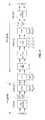
- FIG. 1depicts a portion of a representative dual-carrier double conversion receiver.
- the receiveris operative in an LTE downlink employing intra-band, non-contiguous carrier aggregation, although the principles of the present invention are applicable to other receivers and systems.
- the receiverreceives a composite, carrier aggregation signal at an antenna, which is low-noise amplified.
- the receiverincludes an RF LO frequency generator and an IF LO frequency generator.
- An RF down-convertercomprises two mixers, driven by two corresponding RF LO frequency signals in Quadrature phase, and low-pass filters. The resulting IF signals are then further mixed with IF LO frequency signals having different phases.
- the resulting baseband frequency signalsare combined in two receiver branches, or signal processing paths.
- An upper receiver branchreceives and process a signal modulated onto a 20 MHz carrier frequency
- a lower receiver branchreceives and processes a signal modulated onto a non-contiguous, 5 MHz carrier frequency.
- the modulated signalsmay comply with any communication protocol, such as for example Wideband Code Division Multiple Access (WCDMA).
- the communication protocolmay comprise Orthogonal Frequency Division Multiplexing (OFDM).
- OFDMOrthogonal Frequency Division Multiplexing
- a carriermay comprise a single carrier occupying the specified bandwidth (e.g ., a spread-spectrum carrier), or may comprise a plurality of subcarriers which collectively occupy the specified bandwidth.
- a dual-carrier double conversion receiversuch as that depicted in Fig. 1 is the sensitivity to imbalance between the In-phase (I) and Quadrature (Q) components of a received signal (known as IQ imbalance) stemming from the shared, gain- and phase-imbalanced LOs and mixers.
- IQ imbalanceis considered a major impairment source in radio receivers, particularly in OFDM systems.
- IQ imbalancearises from imbalanced RF/analog circuitry, which includes LO, mixer, filter, ADC, etc.
- RF/analog circuitrycan be calibrated by controlling some circuit parameters, or the IQ imbalance can be compensated by digital signal processing in the digital baseband.
- Digital compensation of IQ imbalancehas many advantages over analog calibration. For example, in principle, it can work with any radios, since it does not require a dedicated interface between radio circuitry and digital baseband.
- Major benefits of IQ imbalance compensationare to relax the design requirement on IQ imbalance, and overcome the fundamental limitation of analog components (or, given the same design effort, to improve the receiver performance).
- Digital compensation of IQ imbalanceis also applicable to double conversion receivers for carrier aggregation, including intra-band, non-contiguous carrier aggregation.
- One distinction, as compared to conventional IQ imbalance compensation,is the need for joint compensation over multiple receiver branches receiving and processing multiple carriers. This is unsurprising, considering that IQ imbalance causes inter-carrier coupling, such that signals processed in each receiver branch includes its own carrier, as well as the other carriers (i.e., signals processed in other receiver branches).
- WO-A1-2010/000297discloses an arrangement for processing a received wireless communication signal.
- the arrangementcomprises a frequency offset compensation unit adapted to apply a frequency offset compensation to the received wireless communication signal, determination circuitry adapted to determine one or more adjustment values associated with the frequency offset compensation, and an FFT-unit adapted to transform the frequency offset compensated received signal to a frequency domain.
- the arrangementalso comprises an IQ-imbalance estimator adapted to estimate an IQ-imbalance, and an IQ-imbalance compensation unit adapted to perform IQ-imbalance compensation of the received wireless communication signal based on the estimated IQ-imbalance. At least one of the IQ-imbalance estimator and the IQ-imbalance compensation unit is adapted to base its operation on the one or more adjustment values.
- Corresponding method and computer program productare also disclosed, application both to OFDM and non OFDM signals.
- US-B1-7433298discloses signal processing methods and apparatus which incorporate I/Q imbalance compensation based on most likely estimates of the I/Q imbalance between the I and Q components of a baseband signal. Most likely estimates of the common phase error may also be used to compensate the initial channel estimates to further improve receiver performance. Though applicable to any multicarrier OFDM communications system, the disclosed methods and apparatus may be conveniently implemented in IEEE 802.11a, IEEE 802.11g, or 802.16a compliant wireless communications systems to reduce the effects of imbalanced I/Q components of baseband signals recovered from inbound RF signals, as well as counter residual frequency offset and phase noise potentially present in such baseband signals.
- digital IQ imbalance estimation and compensationis facilitated (indeed, in some cases, made possible at all), by shaping the frequency response of receiver branches in novel and nonobvious ways, as compared to prior art receivers.
- the frequency response of signal processing elements in at least one receiver branchis set to not fully attenuate received signals in a frequency band of interest.
- the frequency band of interestis greater than the carrier bandwidth of the received signal processed by that receiver branch.
- the received signalis not attenuated, and adjacent interfering signals are partially attenuated. This allows information regarding the interfering signals to appear in an IQ imbalance-induced, inter-carrier image of the signals in another receiver branch, facilitating digital estimation and compensation of IQ imbalance.
- One embodimentrelates to a method of receiving and processing at least first and second communication signals concurrently in respective first and second branches of a receiver.
- the first signalis modulated onto a first carrier having a first bandwidth
- the second signalis modulated onto a second carrier having a second bandwidth.
- the first and second signalsare received.
- the frequency response of signal processing elements in the first receiver branchis set to a frequency response sufficient to not attenuate at least the first signal, and the first signal is processed in the first receiver branch.
- the frequency response of signal processing elements in the second receiver branchis set to a frequency response sufficient to not fully attenuate received signals within a frequency band of interest, the width of which is greater than the carrier bandwidth of the second signal, and the second signal is processed in the second receiver branch.
- the imbalance between I and Q components of the first and second received signalsis estimated, and the estimated IQ imbalance is jointly compensated over the first and second received signals.
- Another embodimentrelates to a receiver operative to receive at least first and second communication signals.
- the first signalis modulated onto a first carrier having a first bandwidth
- the second signalis modulated onto a second carrier having a second bandwidth.
- the receiverincludes a first receiver branch comprising signal processing elements having a first frequency response and operative to receive and process the first signal.
- the receiveralso includes a second receiver branch comprising signal processing elements having a second frequency response and operative to receive and process the second signal.
- the frequency response of signal processing elements in the second receiver branchis sufficient to not fully attenuate received signals within a frequency band of interest, the width of which is greater than the carrier bandwidth of the second signal.
- Digital compensation of IQ imbalanceincludes two steps: imbalance estimation and imbalance compensation. This is also the case for carrier aggregation. Details of digital compensation of IQ imbalance for carrier aggregation are presented in pending U.S. Patent Application Serial No. 13/045,386 .
- a double conversion receivercan be modeled as shown in Figure 2 .
- the transmitterresides in an eNodeB, and includes digital Finite Impulse Response (FIR) filters and analog pulse shape filters (PSF).
- FIRdigital Finite Impulse Response
- PSFanalog pulse shape filters
- the frequency responses of the pulse shape filter for the two carriersare represented by H ta 1 ( f ) and H ta 2 ( f ) .
- the transmitted signals for the two carrierspropagate through multipath fading channels (CH) represented by H ch 1 ( f ) and H ch 2 ( f ) .
- CHmultipath fading channels
- the receiverresides in UE, and includes RF mixers with imbalance parameters K 1 and K 2 , analog IF filters, IF mixers with imbalance parameters J i + , and J i - , analog channel selection filters (CSF) represented by H ra 1 ( f ) and H ra 2 ( f ), and FIR filters.
- the digital baseband partincluding OFDM processing, is omitted for simplicity, but the model assumes the digital baseband, since embodiments of the present invention involve digital compensation of IQ imbalance.
- the double conversion receiverhas a separate branch for each carrier. Assume that all the filters are perfectly balanced within a branch. In other words, there is no intra-carrier imbalance, which is conventionally called IQ imbalance (in practice the IQ imbalance arises largely from the RF mixing stage).
- Q a ( f )represents the analog part only, although it is possible to include the digital part, i.e., the FIR filters of both transmitter and receiver.
- the second matrix of the right-hand side of equation (2), P 1 + f P 2 + f P 3 + f P 4 + f P 2 + * - f P 1 + * - f P 4 + * - f P 3 + * - f P 1 - f P 2 - f P 3 - f P 4 - f P 2 - * - f P 1 - * - f P 4 - * - f P 3 - * - f P 3 - * - frepresents the frequency response contributed by RF mixing stage, IF filter and IF mixing stage.
- the compensated signal from equation (5) Z 1 f Z 2 * - f Z 1 f Z 2 * - fincludes the "distortion" given by analog filters and multipath fading, it can be compensated (also known as being “equalized”) by conventional digital baseband processing. That is, there is no need for inter-carrier processing (as opposed to equation (5)), since it does not introduces any IQ imbalance.
- the IQ imbalanceis called frequency-independent, in the sense that the IQ imbalance parameters that should be estimated are frequency-independent. This eases the IQ imbalance compensation. It also eases the imbalance estimation significantly, since the observation over a small fraction of the bandwidth may suffice. More importantly, it is sometimes impossible to estimate frequency-dependent IQ imbalance, e.g., if the pilot signal does not cover the entire bandwidth. Accordingly, it is quite beneficial to keep the IQ imbalance frequency-independent.
- inter-carrier imbalancemay exist, possibly because of the channel selection filters with frequency responses tuned to different bandwidths.
- the frequency response of each branchis determined by the bandwidth of the carrier that the branch receives.
- the respective receiver branchesmay not have exactly the same frequency response, primarily because of circuit component mismatch introduced in manufacturing, but also due to non-symmetric chip layout. The former can be seen as intentional imbalance, while the latter can be seen as unintentional imbalance.
- Q a ( f )becomes ill-conditioned for a certain fraction of bandwidth, i.e., where the receiver branch processing the narrow-bandwidth carrier is attenuating, while the receiver branch processing the wide-bandwidth carrier is not attenuating.
- Thisis the situation depicted in Figure 1 , where the first signal, received and processed by the first (upper) receiver branch, has a 20 MHz carrier bandwidth and the second signal, received and processed by the second (lower) receiver branch, has a 5 MHz bandwidth.
- the received signal in each receiver branchis depicted, together with the image of the signal received in the other receiver branch, due to IQ imbalance-induced, inter-carrier coupling (as indicated, the image is in the form of the complex conjugate of the signal processed by the other receiver branch).
- the frequency response of signal processing elements in the receiver branchis indicated as a dashed line, depicting signal attenuation as a function of frequency, on the signal diagrams.
- Fig. 3Adepicts the first (20 MHz) signal in the first receiver branch (upper figure), together with the image of the second (5 MHz) signal (lower figure).
- Fig. 3Bdepicts the second (5 MHz) signal (upper figure), together with the image of the first (20 MHz) signal (lower figure).
- the frequency response of signal processing elementsprimarily the channel selection filter
- the frequency response of signal processing elements in the second receiver branchis set to 5 MHz.
- the frequency response of the receiver branchespasses the desired signal, and attenuates nearby interfering signals. This is desirable, and hence comprises the conventional practice, since the interference does not convey any relevant communication information and, moreover, may saturate the ADC or make the quantization error stronger.
- IQ imbalance compensationis impossible, due to the loss of information in the attenuated portions of the received signal(s).
- the image of adjacent channel interferencethat is, the interference adjacent to the second, 5 MHz signal
- the signal processing elements in the first receiver branchhave a frequency response of 20 MHz.
- Fig. 3Bone sees that the corresponding information about the 20 MHz signal is attenuated from the image in the second receiver branch due to the narrower frequency response (5 MHz) of signal processing elements in the second branch.
- digital compensation of IQ imbalanceis impossible, because required information is lost due to the attenuation.
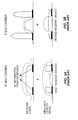
- FIGS. 4A and 4Bdepict this embodiment.
- the frequency response of signal processing elements in the first receiver branch, processing the 20 MHz carrier bandwidth signalis set to 20 MHz, as depicted in Figure 4A.
- Figure 4Bdepicts a hybrid frequency response of signal processing elements in the second receiver branch, which receives and processes a 5 MHz carrier bandwidth signal, together with significant interfering signals outside of the 5 MHz carrier bandwidth.
- the interfering signalsare not fully attenuated.
- a "frequency band of interest”includes both the carrier bandwidth of the second signal (e.g., 5 MHz), and interfering signals outside of the carrier bandwidth of the second signal. Within the frequency band of interest, received signals are not fully attenuated. In particular, the second signal is not attenuated at all (that is, across its carrier bandwidth of 5 MHz), and the interfering signals outside of the carrier bandwidth of the second signal are partially attenuated.
- the interfering signalsappear in the IQ imbalance-caused, inter-carrier coupled image in the first receiver branch (i.e., Fig. 4A , lower signal).
- the interfering signalsare partially attenuated in the second receiver branch ( Fig. 4B , upper signal), so as not to increase the quantization error (by swamping the ADC) in the second receiver branch above an acceptable level (i.e., above a predetermined quantization error threshold).
- the overall width of the frequency response pass-bandis at least as wide as the carrier bandwidth of the wider received signal (e.g., the 20 MHz, signal in the first receiver branch).
- thisis not a limitation of the present invention.
- signals received and processed in the second receiver branchare not fully attenuated within a frequency band of interest, which includes the second signal carrier bandwidth and interfering signals outside the second signal carrier bandwidth.
- not fully attenuatedencompasses (possible) partial attenuation for some signals within the frequency band of interest, such as the interfering signals, as well as no attenuation for the primary signal ( e.g., 5 MHz) within the frequency band of interest.
- the partial attenuation of surrounding interfering signals within the frequency band of interestaddresses a problem that may be significant if the frequency response in the second receiver branch were simply widened out to include the interfering signals, with no attenuation.
- the Analog-to-Digital Converter(ADC) becomes susceptible to quantization error, since the Variable Gain Amplifier (VGA) reduces the gain, in response to the interfering signals, to avoid saturation. Accordingly, the quantization error becomes relatively more dominant. This can be critical when the interference has an extremely high power (compared to the dynamic range of ADC). This problem can be alleviated to a certain extent by increasing ADC resolution, possibly, in an adaptive manner.
- the receiverwhen strong interference is detected (i.e., interference with power above a pre-defined threshold, but low enough to be accommodated by the maximum ADC resolution), the receiver increases the ADC resolution to allow the interference to pass through ADC, and hence be available for use in digital IQ imbalance compensation (of the 20-MHz branch).
- One drawback of this approachis increased power consumption.
- partial attenuation of the interfering signalswith no attenuation of the desired signal, as depicted in Figure 4B , allows for the information of the interfering signals to appear in the image on the 20 MHz receiver branch, without introducing quantization error in the ADC on the 5 MHz receiver branch.
- the embodiment of Figures 4A, 4Boffers a more elegant solution, in some cases, to the interference conundrum than does increasing ADC resolution.
- the degree of partial attenuation of interfering signalsis adaptively determined, such as based on the ADC quantization error in the second receiver branch for various levels of attenuation.
- the power level of interferenceis measured or estimated prior to applying any filtering on receiver branch receiving and processing the narrower carrier bandwidth signal. If IQ imbalance compensation is necessary, interfering signals outside the carrier bandwidth of the primary received signal are attenuated only as necessary such that any increased quantization error due to the VGA control is within a performance margin (i.e., a predetermined quantization error threshold).
- signals received and processed in the second receiver branchare not attenuated at all within the frequency band of interest, as depicted in Figures 5A and 5B .
- the interfering signals in the second receiver branchdo not adversely impact quantization (that is, quantization error remains below an applicable threshold)
- thispreserves the maximum amount of information in the regions where
- the frequency response of signal processing elements in the second receiver branchis less than that in the first receiver branch. That is, the frequency band of interest is wide enough to include the carrier bandwidth of the second signal and also interfering signals, but is not as wide as the carrier bandwidth of the first signal.
- Figure 6depicts a dual-branch, double-conversion receiver operative in a carrier aggregation environment, receiving and processing a first signal having a carrier bandwidth of 20 MHz in a first receiver branch, and a second signal having a carrier bandwidth of 5 MHz in a second receiver branch.
- Signal processing elements in the first receiver branchare controlled to have a frequency response equal to the carrier bandwidth of the first signal (i.e., 20 MHz).
- a frequency band of interest in the second receiver branchis defined to include the carrier bandwidth of the second signal (i.e., 5 MHz), as well as interfering signals, yielding a total frequency band of interest in the second receiver branch of 20 MHz.
- signal processing elements in the second receiver branchare controlled to have a frequency response of 20 MHz as well. In this embodiment, no signals within the frequency band of interest in the second receiver branch are attenuated. This yields the maximum information for digital IQ imbalance estimation and compensation.
- FIGS 7A and 7Bdepict conventional frequency response settings in a carrier aggregation environment where signals received on the first and second receiver branches have the same carrier bandwidth. Note that the frequency response of signal processing elements in the second receiver branch is carefully tailored to pass the received signal, but fully attenuate adjacent interfering signals. For example, as depicted, the roll-off (e.g., of the channel selection filter) has a lower slope, as compared to the frequency response of signal processing elements in the first receiver branch. Because the frequency response in the receiver branches differ, the IQ imbalance must be treated as frequency-dependent in terms of both estimation and compensation, since neither equation (4) nor (6) generally holds. Otherwise, the IQ imbalance compensation may fail to remove the IQ imbalance completely. This increases the difficulty in imbalance estimation and compensation.
- the roll-offe.g., of the channel selection filter
- the frequency response of both receiver branchesis set to be exactly the same - that is, both the width of the passband, and the degree of signal attenuation therein, are equal (in the embodiment depicted, no attenuation within the passband).
- calibrationmay be performed to ensure precise equality in frequency response between the branches (that is, the frequency response between the branches varies less than a predetermined frequency response error). Because such calibration is not part of conventional calibration processes, additional hardware resources may be required, as further discussed herein. In receivers including calibration hardware that operates according to a calibration algorithm, the frequency response calibration in support of IQ imbalance estimation and cancellation may simply be an additional procedure to be invoked on power-up, and/or intermittently during operation.
- calibrationis performed by injecting a test signal (e.g., a single-tone signal) into each receiver branch at the output of the IF mixing stage, and the attenuation of the test signal is measured at the output of OFDM processing. The measurement is repeated over the entire frequency band of interest, to test the frequency response of the receiver branch. Signal processing elements in the receiver branches are then adjusted according to the calibration results, to set the frequency response as desired. In receivers having calibration procedures, this process may be included as an additional step.
- a test signale.g., a single-tone signal
- IQ imbalance estimation and compensationare both performed on a per-subcarrier basis.
- a test signalmay be inserted on every subcarrier and, if a pilot is not provided on every subcarrier, decision-directed estimation may be used for the subcarriers without pilots.
- the compensationmay also be applied to each subcarrier.
- the control of frequency response of signal processing elements in (at least) the second receiver branchesis applied to most functional blocks that follow the IF mixing stage.
- the frequency response of the Variable Gain Amplifier (VGA) and channel selection filterare set to not fully attenuate signals in the frequency band of interest.
- the Analog to Digital Conversion (ADC) sampling rate, STF/NTF, quantization level, and the likemust also be configured to operate with the frequency response covering the frequency band of interest.
- ADCAnalog to Digital Conversion
- interpolatorse.g ., Farrow interpolator
- the FFTFast Fourier Transform
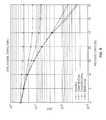
- Figure 8is a graph of the Bit Error Rate (BER) performance of digital IQ imbalance compensation with the frequency response control according to embodiments of the present invention.
- the graphis based on link-simulation of the receiver depicted in Figure 6 .
- Figure 8demonstrates that digital compensation with ideal IQ imbalance estimation and compensation (indicated by "Ideal/Comp") achieves the performance of perfectly-balanced receiver (e.g., the BER drops with increased SNR, as expected).
- the curve labeled "Case I, NoComp”represents the performance of a 20-MHz carrier, assuming a medium-imbalanced radio (40dB IRR) without compensation, in the presence of adjacent channel interference around the 5-MHz carrier with the power of 10dBc and 30dBc.
- the curve labeled "Case II, NoComp”is for a highly-imbalanced radio ( 25dB IRR) in the same condition.
- Figure 9depicts a functional block diagram of portions of a dual-carrier, double-conversion receiver 10 according to embodiments of the present invention.
- the receiver 10is operative in a carrier aggregation environment, and receives at least two signals at an antenna 12.
- the received signalsare processed by a front-end circuit 14 and RF mixer 16.
- two receiver branchesshare the RF 16 and some IF 18 mixer components, outputting the I and Q components of first and second received signals in separate receiver branches.
- the first signalis processed in the first receiver branch by received signal processing elements 22, and the second signal is processed in the second receiver branch by received signal processing elements 26.
- the frequency response of signal processing elements 26 in the second receiver branchis determined in a frequency response determination function 28.
- the frequency response of signal processing elements 26 in the second receiver branchis set to be sufficient (in both frequency and attenuation level) to not fully attenuate received signals within a frequency band of interest, where the width of the frequency band of interest is greater than the carrier bandwidth of the second signal.
- this determinationis made at least partially in consideration of an estimate the interference of interfering signals within the frequency band of interest, as determined by an interference estimation function 30, in combination with an indication of the quantization error for various levels of attenuation of the interfering signals.
- a calibration function 32is operative to inject test signals, across a range of frequencies, into the signal processing elements 22, 26 of the first and second receiver branches, respectively, and monitor the attenuation thereof. In response, the calibration function 32 alters the attenuation, frequency response, or both, of at least signal processing elements 26 in the second receiver branch, via the frequency response determination function 28.
- a per-subcarrier IQ estimation and compensation function 34is operative to perform IQ estimation and compensation on a per-subcarrier basis. In this embodiment, decision-directed estimation may be used for subcarriers that lack pilots.
- one or more of the received signal processing elements 22, 26 of the first and second receiver branches, respectively; the frequency response determination function 28; the interference estimation function 30; the calibration function 32; and the per-subcarrier IQ estimation and compensation function 34may be implemented in hardware (e.g ., as discrete components or appropriately programmed programmable logic); as a combination of hardware and configuring or controlling firmware; as software modules executed on an appropriate processor or digital signal processor (DSP); or any appropriate combination of such technologies.
- DSPdigital signal processor
- Figure 10depicts a method 100 of receiving and processing at least first and second wireless communication signals concurrently in respective first and second branches of a receiver.
- the first signalis modulated onto a first plurality of subcarriers having a first bandwidth
- the second signalis modulated onto a second plurality of subcarriers having a second bandwidth.
- the first and second signalsare received (block 102) and front-end processed.
- the frequency response of signal processing elements in the first receiver branchis set to a width sufficient to not attenuate at least the first signal (i.e., the carrier bandwidth of the first signal) (block 104).
- the first signalis processed in the first receiver branch (block 106).
- the frequency response of signal processing elements in the second receiver branchis set to a width sufficient to not fully attenuate received signals within a frequency band of interest.
- the frequency band of interestis defined as having a width greater than the carrier bandwidth of the second signal (block 108) and may include interfering signals adjacent to the second signal carrier bandwidth.
- the second signalis processed in the second receiver branch (block 110).
- the IQ imbalanceis then estimated (block 112) and jointly compensated between the first and second receiver branches (block 114).
- Embodiments of the present inventionpresent numerous advantages over frequency response shaping for multi-carrier receivers of the prior art.
- IQ imbalancecan be compensated almost completely. This particularly true in the presence of strong adjacent channel interference.
- conventional receiversexperience severe error floor, as shown in Figure 8 .
- IQ imbalance estimation and compensationrelaxes the design requirement dramatically. Without such IQ imbalance compensation, the IRR needs to be as high as 63dB in order to support 64QAM in the presence of 30dBc interference.
Landscapes
- Engineering & Computer Science (AREA)
- Signal Processing (AREA)
- Computer Networks & Wireless Communication (AREA)
- Physics & Mathematics (AREA)
- Electromagnetism (AREA)
- Noise Elimination (AREA)
- Digital Transmission Methods That Use Modulated Carrier Waves (AREA)
- Circuits Of Receivers In General (AREA)
- Mobile Radio Communication Systems (AREA)
- Monitoring And Testing Of Transmission In General (AREA)
Description
- The present invention relates generally to wireless communications, and in particular to a method of mitigating IQ imbalance in multi-carrier receivers in carrier aggregation systems.
- In order to achieve higher peak data rates in future wireless networks, simultaneous transmission and reception of multiple carriers, referred to as carrier aggregation, is considered as a key element. The Third Generation Partnership Project (3GPP) has been standardizing the carrier aggregation for Long Term Evolution (LTE), as described in a paper byG. Yuan, X. Zhang, Wang and Y. Yang, titled "Carrier aggregation for LTE-Advanced mobile communication systems," published in IEEE Commun. Mag., vol. 48, no. 2, pp.88-93, Feb. 2010.
- From the perspective of mobile terminals, carrier aggregation poses unprecedented design challenges, especially when multiple, non-contiguous carriers need to be transmitted and received simultaneously.
- Regarding the receiver architectures of mobile terminals, a direct conversion receiver is well suited for carrier aggregation. Although direct conversion receiver has gained much popularity recently, as indicated in the book,RF Microelectronics, by B. Razavi, Upper Saddle River, NJ, Prentice-Hall, 1998, each carrier inevitably requires an individual receiver, thereby leading to inefficient implementation. On the other hand, a wideband IF double conversion receiver is known, as described in the paper byA. Springer, L. Maurer and R. Weigel, titled "RF system concepts for highly integrated RFICs for W-CDMA mobile radio terminals," published in IEEE Trans. Microw. Theory and Tech., vol. 50, no. 1, pp. 254-267, Jan. 2002.
- The wideband IF double conversion receiver reuses both the RF mixing stage and IF mixing stage (i.e., local oscillators, or LOs, and mixers), allowing for cost-efficient and power-efficient implementation. Moreover, it retains many of the advantages of the direction conversion receiver, for example, highly-programmable channel selection essential to aggressive carrier aggregation.
- The double conversion receiver architecture may be applied to multi-carrier reception. In,e.g., a dual-carrier double conversion receiver, one receiver branch may receive and process a first carrier, while another receiver branch receives and processes a second carrier. By selecting appropriate LO frequencies and mixer parameters, the second receiver branch may share LOs and mixers with the first branch, to conserve hardware.
Figure 1 depicts a portion of a representative dual-carrier double conversion receiver. In this particular example, the receiver is operative in an LTE downlink employing intra-band, non-contiguous carrier aggregation, although the principles of the present invention are applicable to other receivers and systems. The receiver, in this example, receives a composite, carrier aggregation signal at an antenna, which is low-noise amplified. The receiver includes an RF LO frequency generator and an IF LO frequency generator. An RF down-converter comprises two mixers, driven by two corresponding RF LO frequency signals in Quadrature phase, and low-pass filters. The resulting IF signals are then further mixed with IF LO frequency signals having different phases. The resulting baseband frequency signals are combined in two receiver branches, or signal processing paths. An upper receiver branch receives and process a signal modulated onto a 20 MHz carrier frequency, while a lower receiver branch receives and processes a signal modulated onto a non-contiguous, 5 MHz carrier frequency.- The modulated signals may comply with any communication protocol, such as for example Wideband Code Division Multiple Access (WCDMA). In some embodiments, the communication protocol may comprise Orthogonal Frequency Division Multiplexing (OFDM). As known in the art, OFDM signals are modulated onto a plurality of subcarriers which collectively occupy the carrier bandwidth. As used herein, "carrier bandwidth" refers to the frequency of a carrier onto which one or more signals is modulated. A carrier may comprise a single carrier occupying the specified bandwidth (e.g., a spread-spectrum carrier), or may comprise a plurality of subcarriers which collectively occupy the specified bandwidth.
- One drawback a dual-carrier double conversion receiver such as that depicted in
Fig. 1 is the sensitivity to imbalance between the In-phase (I) and Quadrature (Q) components of a received signal (known as IQ imbalance) stemming from the shared, gain- and phase-imbalanced LOs and mixers. IQ imbalance is considered a major impairment source in radio receivers, particularly in OFDM systems. - IQ imbalance arises from imbalanced RF/analog circuitry, which includes LO, mixer, filter, ADC, etc. RF/analog circuitry can be calibrated by controlling some circuit parameters, or the IQ imbalance can be compensated by digital signal processing in the digital baseband. Digital compensation of IQ imbalance has many advantages over analog calibration. For example, in principle, it can work with any radios, since it does not require a dedicated interface between radio circuitry and digital baseband. Major benefits of IQ imbalance compensation are to relax the design requirement on IQ imbalance, and overcome the fundamental limitation of analog components (or, given the same design effort, to improve the receiver performance).
- Digital compensation of IQ imbalance is also applicable to double conversion receivers for carrier aggregation, including intra-band, non-contiguous carrier aggregation. One distinction, as compared to conventional IQ imbalance compensation, is the need for joint compensation over multiple receiver branches receiving and processing multiple carriers. This is unsurprising, considering that IQ imbalance causes inter-carrier coupling, such that signals processed in each receiver branch includes its own carrier, as well as the other carriers(i.e., signals processed in other receiver branches).
WO-A1-2010/000297 discloses an arrangement for processing a received wireless communication signal. The arrangement comprises a frequency offset compensation unit adapted to apply a frequency offset compensation to the received wireless communication signal, determination circuitry adapted to determine one or more adjustment values associated with the frequency offset compensation, and an FFT-unit adapted to transform the frequency offset compensated received signal to a frequency domain. The arrangement also comprises an IQ-imbalance estimator adapted to estimate an IQ-imbalance, and an IQ-imbalance compensation unit adapted to perform IQ-imbalance compensation of the received wireless communication signal based on the estimated IQ-imbalance. At least one of the IQ-imbalance estimator and the IQ-imbalance compensation unit is adapted to base its operation on the one or more adjustment values. Corresponding method and computer program product are also disclosed, application both to OFDM and non OFDM signals.US-B1-7433298 discloses signal processing methods and apparatus which incorporate I/Q imbalance compensation based on most likely estimates of the I/Q imbalance between the I and Q components of a baseband signal. Most likely estimates of the common phase error may also be used to compensate the initial channel estimates to further improve receiver performance. Though applicable to any multicarrier OFDM communications system, the disclosed methods and apparatus may be conveniently implemented in IEEE 802.11a, IEEE 802.11g, or 802.16a compliant wireless communications systems to reduce the effects of imbalanced I/Q components of baseband signals recovered from inbound RF signals, as well as counter residual frequency offset and phase noise potentially present in such baseband signals.- According to one or more embodiments of the present invention described and claimed herein, digital IQ imbalance estimation and compensation is facilitated (indeed, in some cases, made possible at all), by shaping the frequency response of receiver branches in novel and nonobvious ways, as compared to prior art receivers. In particular, in a multi-carrier receiver, the frequency response of signal processing elements in at least one receiver branch is set to not fully attenuate received signals in a frequency band of interest. The frequency band of interest is greater than the carrier bandwidth of the received signal processed by that receiver branch. In some embodiments, the received signal is not attenuated, and adjacent interfering signals are partially attenuated. This allows information regarding the interfering signals to appear in an IQ imbalance-induced, inter-carrier image of the signals in another receiver branch, facilitating digital estimation and compensation of IQ imbalance.
- One embodiment relates to a method of receiving and processing at least first and second communication signals concurrently in respective first and second branches of a receiver. The first signal is modulated onto a first carrier having a first bandwidth, and the second signal is modulated onto a second carrier having a second bandwidth. The first and second signals are received. The frequency response of signal processing elements in the first receiver branch is set to a frequency response sufficient to not attenuate at least the first signal, and the first signal is processed in the first receiver branch. The frequency response of signal processing elements in the second receiver branch is set to a frequency response sufficient to not fully attenuate received signals within a frequency band of interest, the width of which is greater than the carrier bandwidth of the second signal, and the second signal is processed in the second receiver branch. The imbalance between I and Q components of the first and second received signals is estimated, and the estimated IQ imbalance is jointly compensated over the first and second received signals.
- Another embodiment relates to a receiver operative to receive at least first and second communication signals. The first signal is modulated onto a first carrier having a first bandwidth, and the second signal is modulated onto a second carrier having a second bandwidth. The receiver includes a first receiver branch comprising signal processing elements having a first frequency response and operative to receive and process the first signal. The receiver also includes a second receiver branch comprising signal processing elements having a second frequency response and operative to receive and process the second signal. The frequency response of signal processing elements in the second receiver branch is sufficient to not fully attenuate received signals within a frequency band of interest, the width of which is greater than the carrier bandwidth of the second signal.
Figure 1 is a functional circuit schematic of a dual-carrier, double-conversion receiver according to the prior art.Figure 2 is a functional block diagram of a communication signal path and various sources of signal impairments.Figures 3A and 3B depict conventional frequency response shaping for dual-carrier receivers processing signals having different carrier bandwidths.Figures 4A and 4B depict frequency response shaping for a receiver branch according to one embodiment of the present invention.Figures 5A and 5B depict frequency response shaping for a receiver branch according to one embodiment of the present invention.Figure 6 is a functional circuit schematic of a dual-carrier, double-conversion receiver implementing frequency response shaping according to one embodiment of the present invention.Figures 7A and 7B depict conventional frequency response shaping for dual-carrier receivers processing signals having the same carrier bandwidths.Figures 7C and 7D depict frequency response shaping for a receiver processing signals having the same carrier bandwidths according to one embodiment of the present invention.Figure 8 is a graph of multi-carrier receiver performance under various frequency response shaping conditions.Figure 9 is a functional block diagram of a multi-carrier wireless communication receiver according to embodiments of the present invention.Figure 10 is a flow diagram of a method of receiving and processing two wireless communication signals concurrently.- Digital compensation of IQ imbalance includes two steps: imbalance estimation and imbalance compensation. This is also the case for carrier aggregation. Details of digital compensation of IQ imbalance for carrier aggregation are presented in pending
U.S. Patent Application Serial No. 13/045,386 . - A double conversion receiver can be modeled as shown in
Figure 2 . The transmitter resides in an eNodeB, and includes digital Finite Impulse Response (FIR) filters and analog pulse shape filters (PSF). The frequency responses of the pulse shape filter for the two carriers are represented byHta1(f) andHta2(f). The transmitted signals for the two carriers propagate through multipath fading channels (CH) represented byHch1(f) andHch2(f). The receiver resides in UE, and includes RF mixers with imbalance parametersK1 andK2, analog IF filters, IF mixers with imbalance parameters

- As exemplified in
Figure 1 , the double conversion receiver has a separate branch for each carrier. Assume that all the filters are perfectly balanced within a branch. In other words, there is no intra-carrier imbalance, which is conventionally called IQ imbalance (in practice the IQ imbalance arises largely from the RF mixing stage). The received signal of the two branches,Y1(f) andY2(f), are represented as
where the frequency response of transceiver is modeled by a frequency-dependent matrixQa(f) defined as
- For simplicity,Qa(f) represents the analog part only, although it is possible to include the digital part,i.e., the FIR filters of both transmitter and receiver. Here, the second matrix of the right-hand side of equation (2),

represents the frequency response contributed by RF mixing stage, IF filter and IF mixing stage. - If the two carriers have the same bandwidth, and the two channel selection filters are designed to have exactly the same bandwidth - that is, there is no inter-carrier imbalance (more accurately, inter-branch imbalance) in the channel selection filters,i.e.,

then equation (2) can be re-written as
- Assuming that all the IQ imbalance parameters are estimated accurately, the IQ imbalance can be compensated completely as

- Even though the compensated signal from equation (5)

includes the "distortion" given by analog filters and multipath fading, it can be compensated (also known as being "equalized") by conventional digital baseband processing. That is, there is no need for inter-carrier processing (as opposed to equation (5)), since it does not introduces any IQ imbalance. - If the IF filter is sufficiently balanced (or it has significantly less impact than the other imbalance sources, such as RF mixer and IF mixer), the frequency response contributed by RF mixing stage, IF filter and IF mixing stage usually becomes frequency-flat. That is,

- In this case, the IQ imbalance is called frequency-independent, in the sense that the IQ imbalance parameters that should be estimated are frequency-independent. This eases the IQ imbalance compensation. It also eases the imbalance estimation significantly, since the observation over a small fraction of the bandwidth may suffice. More importantly, it is sometimes impossible to estimate frequency-dependent IQ imbalance, e.g., if the pilot signal does not cover the entire bandwidth. Accordingly, it is quite beneficial to keep the IQ imbalance frequency-independent.
- In many of the existing remedies for IQ imbalance, it is assumed that all the receiver branches have exactly the same frequency response. In other words, when it comes to IQ imbalance, the inter-carrier imbalance (in terms of bandwidth) is not of interest, since it is the intra-carrier imbalance(i.e., IQ imbalance) that causes the detrimental coupling.
- In practice, however, inter-carrier imbalance may exist, possibly because of the channel selection filters with frequency responses tuned to different bandwidths. For example, it is likely that the carriers with different bandwidths are aggregated together. In this case, the frequency response of each branch is determined by the bandwidth of the carrier that the branch receives. Also, even when the carriers have the same bandwidth, the respective receiver branches may not have exactly the same frequency response, primarily because of circuit component mismatch introduced in manufacturing, but also due to non-symmetric chip layout. The former can be seen as intentional imbalance, while the latter can be seen as unintentional imbalance.
- If the carriers have different bandwidths,Qa(f) becomes ill-conditioned for a certain fraction of bandwidth,i.e., where the receiver branch processing the narrow-bandwidth carrier is attenuating, while the receiver branch processing the wide-bandwidth carrier is not attenuating. This is the situation depicted in
Figure 1 , where the first signal, received and processed by the first (upper) receiver branch, has a 20 MHz carrier bandwidth and the second signal, received and processed by the second (lower) receiver branch, has a 5 MHz bandwidth. The received signal in each receiver branch is depicted, together with the image of the signal received in the other receiver branch, due to IQ imbalance-induced, inter-carrier coupling (as indicated, the image is in the form of the complex conjugate of the signal processed by the other receiver branch). The frequency response of signal processing elements in the receiver branch is indicated as a dashed line, depicting signal attenuation as a function of frequency, on the signal diagrams. - These signal diagrams are depicted in greater detail in
Figure 3 , whereFig. 3A depicts the first (20 MHz) signal in the first receiver branch (upper figure), together with the image of the second (5 MHz) signal (lower figure). Similarly,Fig. 3B depicts the second (5 MHz) signal (upper figure), together with the image of the first (20 MHz) signal (lower figure). As shown, the frequency response of signal processing elements (primarily the channel selection filter) in the first receiver branch is set to 20 MHz, and the frequency response of signal processing elements in the second receiver branch is set to 5 MHz. In both cases, but as illustrated only for the second (5 MHz) signal, the frequency response of the receiver branches passes the desired signal, and attenuates nearby interfering signals. This is desirable, and hence comprises the conventional practice, since the interference does not convey any relevant communication information and, moreover, may saturate the ADC or make the quantization error stronger. - However, consider the frequency ranges where |Hra1 (f)|> 0 andHra2 (f) ≈ 0-that is, the frequencies above and below the 5 MHz carrier, where the interfering signals are fully attenuated. In these ranges, from equation (2), the elements of the third and fourth rows ofQa(f) become almost zero, and thusQa(f) is in effect singular. As a result, the compensation in equation (5) leads to severe noise enhancement. Moreover, the required imbalance estimation becomes extremely sensitive to noise, since some of the parameters to estimate are much smaller than the others. This is a critical issue, especially when a strong interference (e.g., the power of which is a few tens of dB higher than that of the desired signal) is placed in the proximity of the narrow-bandwidth carrier, and is coupled to the wide-bandwidth carrier because of inter-carrier coupling introduced by IQ imbalance.
- In some cases, IQ imbalance compensation is impossible, due to the loss of information in the attenuated portions of the received signal(s). For example, as depicted in
Fig. 3A , the image of adjacent channel interference (that is, the interference adjacent to the second, 5 MHz signal) in the first receiver branch is not attenuated, since the signal processing elements in the first receiver branch have a frequency response of 20 MHz. However, consideringFig. 3B , one sees that the corresponding information about the 20 MHz signal is attenuated from the image in the second receiver branch due to the narrower frequency response (5 MHz) of signal processing elements in the second branch. Thus, digital compensation of IQ imbalance is impossible, because required information is lost due to the attenuation. - According to one embodiment, in a carrier aggregation environment where received signals have different carrier bandwidth, digital IQ compensation becomes possible by relaxing the attenuation of interfering signals in the receiver branch processing the more narrowband signal.
Figures 4A and 4B depict this embodiment. As before, the frequency response of signal processing elements in the first receiver branch, processing the 20 MHz carrier bandwidth signal, is set to 20 MHz, as depicted inFigure 4A. Figure 4B depicts a hybrid frequency response of signal processing elements in the second receiver branch, which receives and processes a 5 MHz carrier bandwidth signal, together with significant interfering signals outside of the 5 MHz carrier bandwidth. According to this embodiment, the interfering signals are not fully attenuated. - A "frequency band of interest" includes both the carrier bandwidth of the second signal(e.g., 5 MHz), and interfering signals outside of the carrier bandwidth of the second signal. Within the frequency band of interest, received signals are not fully attenuated. In particular, the second signal is not attenuated at all (that is, across its carrier bandwidth of 5 MHz), and the interfering signals outside of the carrier bandwidth of the second signal are partially attenuated.
- As a result, these interfering signals appear in the IQ imbalance-caused, inter-carrier coupled image in the first receiver branch(i.e.,
Fig. 4A , lower signal). However, the interfering signals are partially attenuated in the second receiver branch (Fig. 4B , upper signal), so as not to increase the quantization error (by swamping the ADC) in the second receiver branch above an acceptable level(i.e., above a predetermined quantization error threshold). As depicted inFigures 4A and 4B , in one embodiment, the overall width of the frequency response pass-band is at least as wide as the carrier bandwidth of the wider received signal(e.g., the 20 MHz, signal in the first receiver branch). However, this is not a limitation of the present invention. - Thus, according to some embodiments, signals received and processed in the second receiver branch are not fully attenuated within a frequency band of interest, which includes the second signal carrier bandwidth and interfering signals outside the second signal carrier bandwidth. As used herein, "not fully attenuated" encompasses (possible) partial attenuation for some signals within the frequency band of interest, such as the interfering signals, as well as no attenuation for the primary signal (e.g., 5 MHz) within the frequency band of interest.
- The partial attenuation of surrounding interfering signals within the frequency band of interest addresses a problem that may be significant if the frequency response in the second receiver branch were simply widened out to include the interfering signals, with no attenuation. In that case, the Analog-to-Digital Converter (ADC) becomes susceptible to quantization error, since the Variable Gain Amplifier (VGA) reduces the gain, in response to the interfering signals, to avoid saturation. Accordingly, the quantization error becomes relatively more dominant. This can be critical when the interference has an extremely high power (compared to the dynamic range of ADC). This problem can be alleviated to a certain extent by increasing ADC resolution, possibly, in an adaptive manner. In other words, when strong interference is detected(i.e., interference with power above a pre-defined threshold, but low enough to be accommodated by the maximum ADC resolution), the receiver increases the ADC resolution to allow the interference to pass through ADC, and hence be available for use in digital IQ imbalance compensation (of the 20-MHz branch). One drawback of this approach is increased power consumption. However, partial attenuation of the interfering signals, with no attenuation of the desired signal, as depicted in
Figure 4B , allows for the information of the interfering signals to appear in the image on the 20 MHz receiver branch, without introducing quantization error in the ADC on the 5 MHz receiver branch. Thus, the embodiment ofFigures 4A, 4B offers a more elegant solution, in some cases, to the interference conundrum than does increasing ADC resolution. - In one embodiment, the degree of partial attenuation of interfering signals is adaptively determined, such as based on the ADC quantization error in the second receiver branch for various levels of attenuation. In this embodiment, the power level of interference is measured or estimated prior to applying any filtering on receiver branch receiving and processing the narrower carrier bandwidth signal. If IQ imbalance compensation is necessary, interfering signals outside the carrier bandwidth of the primary received signal are attenuated only as necessary such that any increased quantization error due to the VGA control is within a performance margin(i.e., a predetermined quantization error threshold).
- In one embodiment, signals received and processed in the second receiver branch are not attenuated at all within the frequency band of interest, as depicted in
Figures 5A and 5B . In situations where the interfering signals in the second receiver branch do not adversely impact quantization (that is, quantization error remains below an applicable threshold), this preserves the maximum amount of information in the regions where |Hra1(f)|>0 andHra2 (f) ≈ 0 , maximizing the effectiveness of digital IQ imbalance compensation. Note that, in the embodiment depicted inFigures 5A and 5B , the frequency response of signal processing elements in the second receiver branch is less than that in the first receiver branch. That is, the frequency band of interest is wide enough to include the carrier bandwidth of the second signal and also interfering signals, but is not as wide as the carrier bandwidth of the first signal. - In general, whether interfering signals in the second receiver branch are partially attenuated or not attenuated, and the whether the frequency band of interest in the second branch is as wide as the carrier bandwidth of the first signal, are independent considerations. The combination of these factors in
Figures 4A-5B is representative only. Figure 6 depicts a dual-branch, double-conversion receiver operative in a carrier aggregation environment, receiving and processing a first signal having a carrier bandwidth of 20 MHz in a first receiver branch, and a second signal having a carrier bandwidth of 5 MHz in a second receiver branch. Signal processing elements in the first receiver branch are controlled to have a frequency response equal to the carrier bandwidth of the first signal(i.e., 20 MHz). A frequency band of interest in the second receiver branch is defined to include the carrier bandwidth of the second signal (i.e., 5 MHz), as well as interfering signals, yielding a total frequency band of interest in the second receiver branch of 20 MHz. Accordingly, signal processing elements in the second receiver branch are controlled to have a frequency response of 20 MHz as well. In this embodiment, no signals within the frequency band of interest in the second receiver branch are attenuated. This yields the maximum information for digital IQ imbalance estimation and compensation.Figures 7A and 7B depict conventional frequency response settings in a carrier aggregation environment where signals received on the first and second receiver branches have the same carrier bandwidth. Note that the frequency response of signal processing elements in the second receiver branch is carefully tailored to pass the received signal, but fully attenuate adjacent interfering signals. For example, as depicted, the roll-off(e.g., of the channel selection filter) has a lower slope, as compared to the frequency response of signal processing elements in the first receiver branch. Because the frequency response in the receiver branches differ, the IQ imbalance must be treated as frequency-dependent in terms of both estimation and compensation, since neither equation (4) nor (6) generally holds. Otherwise, the IQ imbalance compensation may fail to remove the IQ imbalance completely. This increases the difficulty in imbalance estimation and compensation.- In particular, in the absence of equal frequency response between the first and second receiver branches, the IQ imbalance becomes frequency dependent, and equation (6) is not valid. In this case, compensation is performed as

- According to one embodiment, as depicted in
Figures 7C and 7D , in the case of equal-bandwidth carriers, the frequency response of both receiver branches is set to be exactly the same - that is, both the width of the passband, and the degree of signal attenuation therein, are equal (in the embodiment depicted, no attenuation within the passband). - In some embodiments, calibration may be performed to ensure precise equality in frequency response between the branches (that is, the frequency response between the branches varies less than a predetermined frequency response error). Because such calibration is not part of conventional calibration processes, additional hardware resources may be required, as further discussed herein. In receivers including calibration hardware that operates according to a calibration algorithm, the frequency response calibration in support of IQ imbalance estimation and cancellation may simply be an additional procedure to be invoked on power-up, and/or intermittently during operation.
- In one embodiment, calibration is performed by injecting a test signal(e.g., a single-tone signal) into each receiver branch at the output of the IF mixing stage, and the attenuation of the test signal is measured at the output of OFDM processing. The measurement is repeated over the entire frequency band of interest, to test the frequency response of the receiver branch. Signal processing elements in the receiver branches are then adjusted according to the calibration results, to set the frequency response as desired. In receivers having calibration procedures, this process may be included as an additional step.
- Alternatively, in one embodiment, where no inter-carrier calibration is performed, frequency-dependence of IQ imbalance is assumed, and IQ imbalance estimation and compensation are both performed on a per-subcarrier basis. A test signal may be inserted on every subcarrier and, if a pilot is not provided on every subcarrier, decision-directed estimation may be used for the subcarriers without pilots. Once the IQ imbalance parameters are estimated, the compensation may also be applied to each subcarrier.
- In general, the control of frequency response of signal processing elements in (at least) the second receiver branches is applied to most functional blocks that follow the IF mixing stage. For example, in the analog baseband, the frequency response of the Variable Gain Amplifier (VGA) and channel selection filter are set to not fully attenuate signals in the frequency band of interest. The Analog to Digital Conversion (ADC) sampling rate, STF/NTF, quantization level, and the like must also be configured to operate with the frequency response covering the frequency band of interest. In the digital front-end, not only all the digital filters, but also other functions such as interpolators (e.g., Farrow interpolator) must be configured to operate with the frequency response covering the frequency band of interest. In the digital baseband, the Fast Fourier Transform (FFT) function must be configured to operate with the frequency response covering the frequency band of interest.
Figure 8 is a graph of the Bit Error Rate (BER) performance of digital IQ imbalance compensation with the frequency response control according to embodiments of the present invention. In particular, the graph is based on link-simulation of the receiver depicted inFigure 6 .Figure 8 demonstrates that digital compensation with ideal IQ imbalance estimation and compensation (indicated by "Ideal/Comp") achieves the performance of perfectly-balanced receiver(e.g., the BER drops with increased SNR, as expected). InFigure 8 , the curve labeled "Case I, NoComp" represents the performance of a 20-MHz carrier, assuming a medium-imbalanced radio (40dB IRR) without compensation, in the presence of adjacent channel interference around the 5-MHz carrier with the power of 10dBc and 30dBc. The curve labeled "Case II, NoComp" is for a highly-imbalanced radio ( 25dB IRR) in the same condition.Figure 9 depicts a functional block diagram of portions of a dual-carrier, double-conversion receiver 10 according to embodiments of the present invention. Thereceiver 10 is operative in a carrier aggregation environment, and receives at least two signals at anantenna 12. The received signals are processed by a front-end circuit 14 andRF mixer 16. As depicted in greater detail inFigure 6 , two receiver branches share theRF 16 and some IF 18 mixer components, outputting the I and Q components of first and second received signals in separate receiver branches. The first signal is processed in the first receiver branch by receivedsignal processing elements 22, and the second signal is processed in the second receiver branch by receivedsignal processing elements 26.- The frequency response of
signal processing elements 26 in the second receiver branch is determined in a frequencyresponse determination function 28. As described herein, the frequency response ofsignal processing elements 26 in the second receiver branch is set to be sufficient (in both frequency and attenuation level) to not fully attenuate received signals within a frequency band of interest, where the width of the frequency band of interest is greater than the carrier bandwidth of the second signal. In one embodiment, this determination is made at least partially in consideration of an estimate the interference of interfering signals within the frequency band of interest, as determined by aninterference estimation function 30, in combination with an indication of the quantization error for various levels of attenuation of the interfering signals. - In one embodiment, a
calibration function 32 is operative to inject test signals, across a range of frequencies, into thesignal processing elements calibration function 32 alters the attenuation, frequency response, or both, of at leastsignal processing elements 26 in the second receiver branch, via the frequencyresponse determination function 28. In one embodiment, a per-subcarrier IQ estimation andcompensation function 34 is operative to perform IQ estimation and compensation on a per-subcarrier basis. In this embodiment, decision-directed estimation may be used for subcarriers that lack pilots. - Those of skill in the art will appreciate that one or more of the received
signal processing elements response determination function 28; theinterference estimation function 30; thecalibration function 32; and the per-subcarrier IQ estimation andcompensation function 34 may be implemented in hardware (e.g., as discrete components or appropriately programmed programmable logic); as a combination of hardware and configuring or controlling firmware; as software modules executed on an appropriate processor or digital signal processor (DSP); or any appropriate combination of such technologies. Figure 10 depicts amethod 100 of receiving and processing at least first and second wireless communication signals concurrently in respective first and second branches of a receiver. The first signal is modulated onto a first plurality of subcarriers having a first bandwidth, and the second signal is modulated onto a second plurality of subcarriers having a second bandwidth. The first and second signals are received (block 102) and front-end processed. The frequency response of signal processing elements in the first receiver branch is set to a width sufficient to not attenuate at least the first signal(i.e., the carrier bandwidth of the first signal) (block 104). The first signal is processed in the first receiver branch (block 106). The frequency response of signal processing elements in the second receiver branch is set to a width sufficient to not fully attenuate received signals within a frequency band of interest. The frequency band of interest is defined as having a width greater than the carrier bandwidth of the second signal (block 108) and may include interfering signals adjacent to the second signal carrier bandwidth. The second signal is processed in the second receiver branch (block 110). The IQ imbalance is then estimated (block 112) and jointly compensated between the first and second receiver branches (block 114).- Embodiments of the present invention present numerous advantages over frequency response shaping for multi-carrier receivers of the prior art. By setting the frequency response of receiver branches processing received signals with narrower carrier bandwidths to cover a frequency band of interest that is wider than the carrier bandwidths, IQ imbalance can be compensated almost completely. This particularly true in the presence of strong adjacent channel interference. In sharp contrast, without effective IQ imbalance compensation as enabled by embodiments of the present invention, conventional receivers experience severe error floor, as shown in
Figure 8 . - IQ imbalance estimation and compensation according to embodiments of the present invention relaxes the design requirement dramatically. Without such IQ imbalance compensation, the IRR needs to be as high as 63dB in order to support 64QAM in the presence of 30dBc interference.
- By adaptively changing the ADC resolution, the impact of quantization error due to the bandwidth control and the additional power consumption can be minimized.
- By calibrating multiple receiver branches before IQ imbalance estimation and compensation, digital compensation of IQ imbalance may be possible even when the pilot signal is not available over the entire bandwidth.
- By conducting frequency-dependent imbalance estimation and compensation, the impact of inter-carrier imbalance can be mitigated.
- The present invention may, of course, be carried out in other ways than those specifically set forth herein without departing from essential characteristics of the invention. The present embodiments are to be considered in all respects as illustrative and not restrictive, and all changes coming within the meaning of the appended claims are intended to be embraced therein.


Claims (35)
- A method (100) of receiving and processing at least first and second communication signals concurrently in respective first and second branches of a receiver (10), wherein the first signal is modulated onto a first carrier having a first bandwidth, and the second signal is modulated onto a second carrier having a second bandwidth, the method comprising the steps of:receiving (102) the first and second signals;setting (104) the frequency response of signal processing elements in the first receiver branch to a frequency response sufficient to not attenuate at least the first signal;processing (106) the first signal in the first receiver branch;setting (108) the frequency response of signal processing elements in the second receiver branch to a frequency response sufficient to not fully attenuate received signals within a frequency band of interest, the width of which is greater than the carrier bandwidth of the second signal;processing (110) the second signal in the second receiver branch;estimating (112) the imbalance between In-phase I and Quadrature Q components of the first and second received signals; andjointly compensating (114) the estimated IQ imbalance over the first and second received signals.
- The method (100) of claim 1 wherein setting (104, 108) the frequency response of signal processing elements in a receiver branch comprises setting the frequency responses of at least an analog variable gain amplifier and an analog channel selection filter in the receiver branch.
- The method (100) of claim 1 wherein setting (104, 108) the frequency response of signal processing elements in a receiver branch comprises setting the frequency response of digital filters and interpolators in the receiver branch.
- The method (100) of claim 1 wherein setting (104, 108) the frequency response of signal processing elements in a receiver branch comprises configuring a digital baseband Fast Fourier Transformer FFT to operate with the determined frequency response.
- The method (100) of claim 1 wherein the first signal carrier bandwidth is broader than the second signal carrier bandwidth, and wherein setting (108) the frequency response of signal processing elements in the second receiver branch comprises setting the frequency response to be at least as wide as the bandwidth of the first signal.
- The method (100) of claim 5 wherein a frequency response sufficient to not fully attenuate received signals within a frequency band of interest comprises a frequency response sufficient to not attenuate received signals within the frequency band of interest.
- The method (100) of claim 5 wherein a frequency response sufficient to not fully attenuate received signals within a frequency band of interest comprises a frequency response sufficient to not attenuate the second signal, and to partially attenuate interfering signals within the frequency band of interest.
- The method (100) of claim 7 wherein the degree of partial attenuation of interfering signals within the frequency band of interest is determined by the quantization error in the second receiver branch introduced by the interfering signals.
- The method (100) of claim 1 wherein the first and second signal carrier bandwidths are equal, and wherein setting (108) the frequency response of signal processing elements in the second receiver branch comprises setting the frequency response to match the frequency response of signal processing elements in the first receiver branch.
- The method (100) of claim 1 wherein the first signal carrier bandwidth is broader than the second signal carrier bandwidth, and wherein setting (108) the frequency response of signal processing elements in the second receiver branch comprises the steps of:estimating the power level of interference in the first and second signals;if the interference power level is sufficient to increase the interference power originating from IQ imbalance above a predetermined threshold but insufficient to increase quantization error in the second receiver branch above a predetermined quantization error threshold, setting (108) the frequency response of signal processing elements in the second receiver branch to not fully attenuate interfering signals within the frequency band of interest; andotherwise, setting the frequency response of signal processing elements in the second receiver branch equal to the carrier bandwidth of the second signal.
- The method of claim 1 wherein setting (108) the frequency response of signal processing elements in the second receiver branch comprises setting the frequency response to be equal to the frequency response of signal processing elements in the first receiver branch; and further comprising
calibrating the first and second receiver branches to have the same frequency response to within a predetermined frequency response error threshold. - The method of claim 11 wherein calibrating the first and second receiver branches comprises performing the calibration when the receiver is initially powered to an operative state.
- The method of claim 11 wherein calibrating the first and second receiver branches comprises performing the calibration at predetermined intervals.
- The method of claim 11 wherein calibrating the first and second receiver branches comprises injecting a test signal into at least one receiver branch and measuring its attenuation at the output of signal processing in the branch.
- The method of claim 14 wherein the test signal comprises a single-tone signal.
- The method of claim 15 further comprising repeating the calibration test while altering the frequency of the single-tone test signal over the first bandwidth.
- The method of claim 16 wherein the frequency of the single-tone test signal is varied over a subset of subcarriers.
- The method of claim 1 wherein the first and second signals are Orthogonal Frequency Division Multiplexed signals, the first signal is modulated onto a first plurality of subcarriers, the first plurality having a first bandwidth, the second signal is modulated onto a second plurality of subcarriers, the second plurality having a second bandwidth, and:setting (108) the frequency response of signal processing elements in the second receiver branch comprises setting the frequency response equal to the frequency response of signal processing elements in the first receiver branch; andestimating IQ imbalance and compensating the estimated IQ imbalance on a per-subcarrier basis.
- The method of claim 18 wherein estimating IQ imbalance on a per-subcarrier basis comprises injecting a test signal into at least one receiver branch on each subcarrier.
- The method of claim 18 further comprising, for each subcarrier without a pilot signal, using decision-directed IQ estimation.
- A receiver (10) operative to concurrently receive at least first and second communication signals, wherein the first signal is modulated onto a first carrier having a first bandwidth, and the second signal is modulated onto a second carrier having a second bandwidth, comprising:a first receiver branch comprising signal processing elements (22) having a first frequency response and operative to receive and process the first signal; anda second receiver branch comprising signal processing elements (26) having a second frequency response and operative to receive and process the second signal;wherein the frequency response of signal processing elements (26) in the second receiver branch is sufficient to not fully attenuate received signals within a frequency band of interest, the width of which is greater than the carrier bandwidth of the second signal.
- The receiver (10) of claim 21 wherein the frequency response of signal processing elements (26) in the second receiver branch sufficient to not fully attenuate received signals within a frequency band of interest comprises a frequency response sufficient to not attenuate received signals within the frequency band of interest.
- The receiver (10) of claim 21 wherein the frequency response of signal processing elements (26) in the second receiver branch sufficient to not fully attenuate received signals within a frequency band of interest comprises a frequency response sufficient to partially attenuate interfering signals within the frequency band of interest.
- The receiver (10) of claim 23 wherein the signal processing elements (26) in the second receiver branch are operative to determine the degree of attenuation of interfering signals within the frequency band of interest by the quantization error in the second receiver branch introduced by the interfering signals.
- The receiver (10) of claim 23 wherein the first and second signal carrier bandwidths are equal, and wherein the signal processing elements (26) in the second receiver branch are operative to set the frequency response of signal processing elements (26) in the second receiver branch equal to the frequency response of signal processing elements (22) in the first receiver branch.
- The receiver (10) of claim 21 further comprising:an interference power estimator (30) operative to estimate the power level of interference in the first and second signals; andan adaptive frequency response function operative to adapt the frequency response of signal processing elements (26) in the second receiver branch to not fully attenuate interfering signals within the frequency band of interest if the interference power level is sufficient to increase IQ imbalance above a predetermined IQ imbalance threshold but insufficient to increase quantization error in the second receiver branch above a predetermined quantization error threshold, and operative to set the frequency response of signal processing elements (26) in the second receiver branch equal to the second bandwidth otherwise.
- The receiver (10) of claim 21 wherein the frequency response of signal processing elements (26) in the second receiver branch equals the frequency response of signal processing elements (22) in the first receiver branch, and further comprising:a calibration unit (32) operative to calibrate the first and second receiver branches to have the same frequency response to within a predetermined frequency response error threshold.
- The receiver (10) of claim 27 wherein the calibration unit (32) is operative to perform the frequency response calibration when the receiver (10) is initially powered to an operative state.
- The receiver (10) of claim 27 wherein the calibration unit (32) is operative to perform the frequency response calibration at predetermined intervals.
- The receiver (10) of claim 27 wherein the calibration unit (32) is operative to perform the frequency response calibration by injecting a test signal into at least one receiver branch and measuring its attenuation at the output of signal processing in the branch.
- The receiver (10) of claim 30 wherein the calibration unit (32) is operative to inject a test signal which comprises a single-tone signal.
- The receiver (10) of claim 30 wherein the calibration unit (32) is operative to repeat the calibration test while altering the frequency of the single-tone test signal over the first bandwidth.
- The receiver (10) of claim 21 wherein the first and second signals are Orthogonal Frequency Division Multiplexed, the first signal is modulated onto a first plurality of subcarriers, the first plurality having a first bandwidth, the second signal is modulated onto a second plurality of subcarriers, the second plurality having a second bandwidth, and the frequency response of signal processing elements (26) in the second receiver branch equals the frequency response of signal processing elements (22) in the first receiver branch, and further comprising:a IQ imbalance estimation and compensation function operative to estimate IQ imbalance and compensate the estimated IQ imbalance on a per-subcarrier basis.
- The receiver of claim 33 wherein the IQ imbalance estimation and compensation function is operative to estimate IQ imbalance on a per-subcarrier basis by injecting a test signal into at least one receiver branch on each sub carrier.
- The receiver of claim 34 wherein the IQ imbalance estimation and compensation function is further operative to use decision-directed IQ estimation for each subcarrier without a pilot signal.
Applications Claiming Priority (4)
| Application Number | Priority Date | Filing Date | Title |
|---|---|---|---|
| US33061210P | 2010-05-03 | 2010-05-03 | |
| US13/045,386US8565352B2 (en) | 2010-05-03 | 2011-03-10 | Digital IQ imbalance compensation for dual-carrier double conversion receiver |
| US13/098,954US8798177B2 (en) | 2010-05-03 | 2011-05-02 | Inter-carrier bandwidth control for mitigating IQ imbalance |
| PCT/US2011/034939WO2011140046A1 (en) | 2010-05-03 | 2011-05-03 | Inter-carrier bandwidth control for mitigating iq imbalance |
Publications (2)
| Publication Number | Publication Date |
|---|---|
| EP2567522A1 EP2567522A1 (en) | 2013-03-13 |
| EP2567522B1true EP2567522B1 (en) | 2015-04-15 |
Family
ID=44544036
Family Applications (2)
| Application Number | Title | Priority Date | Filing Date |
|---|---|---|---|
| EP11723122.5ANot-in-forceEP2567523B1 (en) | 2010-05-03 | 2011-04-20 | Digital iq imbalance compensation for dual-carrier double conversion receiver |
| EP11720650.8AActiveEP2567522B1 (en) | 2010-05-03 | 2011-05-03 | Inter-carrier bandwidth control for mitigating IQ imbalance |
Family Applications Before (1)
| Application Number | Title | Priority Date | Filing Date |
|---|---|---|---|
| EP11723122.5ANot-in-forceEP2567523B1 (en) | 2010-05-03 | 2011-04-20 | Digital iq imbalance compensation for dual-carrier double conversion receiver |
Country Status (8)
| Country | Link |
|---|---|
| US (2) | US8565352B2 (en) |
| EP (2) | EP2567523B1 (en) |
| JP (1) | JP5777704B2 (en) |
| KR (1) | KR101831000B1 (en) |
| CN (2) | CN102870389B (en) |
| DK (1) | DK2567522T3 (en) |
| RU (1) | RU2515282C1 (en) |
| WO (2) | WO2011138697A1 (en) |
Families Citing this family (87)
| Publication number | Priority date | Publication date | Assignee | Title |
|---|---|---|---|---|
| US9026070B2 (en) | 2003-12-18 | 2015-05-05 | Qualcomm Incorporated | Low-power wireless diversity receiver with multiple receive paths |
| US9450665B2 (en) | 2005-10-19 | 2016-09-20 | Qualcomm Incorporated | Diversity receiver for wireless communication |
| US8548096B2 (en)* | 2010-12-31 | 2013-10-01 | Telefonaktiebolaget L M Ericsson (Publ) | Controllable frequency offset for inphase and Quadrature (IQ) imbalance estimation |
| US9887728B2 (en) | 2011-02-03 | 2018-02-06 | The Board Of Trustees Of The Leland Stanford Junior University | Single channel full duplex wireless communications |
| US9331737B2 (en) | 2012-02-08 | 2016-05-03 | The Board Of Trustees Of The Leland Stanford Junior University | Systems and methods for cancelling interference using multiple attenuation delays |
| US10284356B2 (en) | 2011-02-03 | 2019-05-07 | The Board Of Trustees Of The Leland Stanford Junior University | Self-interference cancellation |
| US9178669B2 (en) | 2011-05-17 | 2015-11-03 | Qualcomm Incorporated | Non-adjacent carrier aggregation architecture |
| US9252827B2 (en) | 2011-06-27 | 2016-02-02 | Qualcomm Incorporated | Signal splitting carrier aggregation receiver architecture |
| US9154179B2 (en) | 2011-06-29 | 2015-10-06 | Qualcomm Incorporated | Receiver with bypass mode for improved sensitivity |
| US12081243B2 (en) | 2011-08-16 | 2024-09-03 | Qualcomm Incorporated | Low noise amplifiers with combined outputs |
| EP2579487B1 (en)* | 2011-10-03 | 2014-05-21 | ST-Ericsson SA | Non-contiguous carrier aggregation |
| US8787862B2 (en) | 2011-10-17 | 2014-07-22 | Broadcom Corporation | Method of receiving and receivers |
| GB201119887D0 (en) | 2011-10-17 | 2011-12-28 | Renesas Mobile Corp | Methods of receiving and receivers |
| US8774334B2 (en) | 2011-11-09 | 2014-07-08 | Qualcomm Incorporated | Dynamic receiver switching |
| US10243719B2 (en) | 2011-11-09 | 2019-03-26 | The Board Of Trustees Of The Leland Stanford Junior University | Self-interference cancellation for MIMO radios |
| GB2492495B (en)* | 2011-11-17 | 2014-06-04 | Broadcom Corp | Methods of receiving and receivers |
| GB201119888D0 (en) | 2011-11-17 | 2011-12-28 | Renesas Mobile Corp | Methods of receiving and receivers |
| US9088468B2 (en) | 2012-01-20 | 2015-07-21 | Telefonaktiebolaget L M Ericsson (Publ) | Double conversion dual-carrier radio frequency receiver |
| US9325432B2 (en) | 2012-02-08 | 2016-04-26 | The Board Of Trustees Of The Leland Stanford Junior University | Systems and methods for full-duplex signal shaping |
| US9362958B2 (en) | 2012-03-02 | 2016-06-07 | Qualcomm Incorporated | Single chip signal splitting carrier aggregation receiver architecture |
| US9172402B2 (en) | 2012-03-02 | 2015-10-27 | Qualcomm Incorporated | Multiple-input and multiple-output carrier aggregation receiver reuse architecture |
| US9118439B2 (en)* | 2012-04-06 | 2015-08-25 | Qualcomm Incorporated | Receiver for imbalanced carriers |
| US9686103B2 (en)* | 2012-04-27 | 2017-06-20 | Mediatek Inc. | Method for compensating the frequency dependent phase imbalance |
| US9154356B2 (en) | 2012-05-25 | 2015-10-06 | Qualcomm Incorporated | Low noise amplifiers for carrier aggregation |
| US9226174B2 (en) | 2012-06-09 | 2015-12-29 | Apple Inc. | Improving reception by a wireless communication device |
| US9867194B2 (en) | 2012-06-12 | 2018-01-09 | Qualcomm Incorporated | Dynamic UE scheduling with shared antenna and carrier aggregation |
| US9300420B2 (en) | 2012-09-11 | 2016-03-29 | Qualcomm Incorporated | Carrier aggregation receiver architecture |
| JP5681683B2 (en)* | 2012-09-18 | 2015-03-11 | アンリツ株式会社 | Mobile terminal test apparatus and mobile terminal test method |
| US9543903B2 (en) | 2012-10-22 | 2017-01-10 | Qualcomm Incorporated | Amplifiers with noise splitting |
| US9596065B2 (en) | 2012-10-24 | 2017-03-14 | Qualcomm Incorporated | Enhanced SRS transmission for MIMO operation in LTE-A |
| US9338668B2 (en)* | 2012-11-07 | 2016-05-10 | Qualcomm Incorporated | Gain control for intra-band carrier aggregation |
| US8995591B2 (en) | 2013-03-14 | 2015-03-31 | Qualcomm, Incorporated | Reusing a single-chip carrier aggregation receiver to support non-cellular diversity |
| CN104104454A (en)* | 2013-04-01 | 2014-10-15 | 中兴通讯股份有限公司 | Terminal carrier polymerization test device |
| US9661579B1 (en)* | 2013-05-03 | 2017-05-23 | Marvell International Ltd. | Per-tone power control in OFDM |
| US9397761B2 (en)* | 2013-05-17 | 2016-07-19 | Crfs Limited | RF signal generating device |
| US11163050B2 (en) | 2013-08-09 | 2021-11-02 | The Board Of Trustees Of The Leland Stanford Junior University | Backscatter estimation using progressive self interference cancellation |
| WO2015021461A1 (en) | 2013-08-09 | 2015-02-12 | Kumu Networks, Inc. | Systems and methods for non-linear digital self-interference cancellation |
| US9698860B2 (en) | 2013-08-09 | 2017-07-04 | Kumu Networks, Inc. | Systems and methods for self-interference canceller tuning |
| WO2015021481A2 (en)* | 2013-08-09 | 2015-02-12 | The Board Of Trustees Of The Leland Stanford Junior University | Self-interference cancellation |
| US9036749B2 (en) | 2013-08-09 | 2015-05-19 | Kumu Networks, Inc. | Systems and methods for frequency independent analog self-interference cancellation |
| US9054795B2 (en) | 2013-08-14 | 2015-06-09 | Kumu Networks, Inc. | Systems and methods for phase noise mitigation |
| US10673519B2 (en) | 2013-08-29 | 2020-06-02 | Kuma Networks, Inc. | Optically enhanced self-interference cancellation |
| WO2015031830A1 (en) | 2013-08-29 | 2015-03-05 | Kumu Networks, Inc. | Full-duplex relays |
| US9520983B2 (en) | 2013-09-11 | 2016-12-13 | Kumu Networks, Inc. | Systems for delay-matched analog self-interference cancellation |
| CN104660540B (en)* | 2013-11-21 | 2018-11-16 | 展讯通信(上海)有限公司 | A kind of method for synchronized of LTE system |
| US9774405B2 (en) | 2013-12-12 | 2017-09-26 | Kumu Networks, Inc. | Systems and methods for frequency-isolated self-interference cancellation |
| US9077421B1 (en) | 2013-12-12 | 2015-07-07 | Kumu Networks, Inc. | Systems and methods for hybrid self-interference cancellation |
| US10230422B2 (en) | 2013-12-12 | 2019-03-12 | Kumu Networks, Inc. | Systems and methods for modified frequency-isolation self-interference cancellation |
| US9641126B2 (en) | 2013-12-19 | 2017-05-02 | Qualcomm Incorporated | Systems and methods for I-Q imbalance calibration |
| US9712312B2 (en) | 2014-03-26 | 2017-07-18 | Kumu Networks, Inc. | Systems and methods for near band interference cancellation |
| US11209536B2 (en) | 2014-05-02 | 2021-12-28 | The Board Of Trustees Of The Leland Stanford Junior University | Method and apparatus for tracking motion using radio frequency signals |
| WO2015168941A1 (en)* | 2014-05-09 | 2015-11-12 | 华为技术有限公司 | Signal processing method and apparatus |
| US9276682B2 (en) | 2014-05-23 | 2016-03-01 | Kumu Networks, Inc. | Systems and methods for multi-rate digital self-interference cancellation |
| US9521023B2 (en) | 2014-10-17 | 2016-12-13 | Kumu Networks, Inc. | Systems for analog phase shifting |
| US9712313B2 (en) | 2014-11-03 | 2017-07-18 | Kumu Networks, Inc. | Systems for multi-peak-filter-based analog self-interference cancellation |
| GB2537800B (en)* | 2014-12-22 | 2018-05-30 | Imagination Tech Ltd | IQ imbalance estimator |
| US9673854B2 (en) | 2015-01-29 | 2017-06-06 | Kumu Networks, Inc. | Method for pilot signal based self-inteference cancellation tuning |
| EP3068044A1 (en)* | 2015-03-11 | 2016-09-14 | Nxp B.V. | Module for a radio receiver |
| US10165566B2 (en) | 2015-04-17 | 2018-12-25 | Samsung Electronics Co., Ltd | Transmitter and method using carrier aggregation |
| US10659277B2 (en) | 2015-08-21 | 2020-05-19 | Viasat, Inc. | Method and system in which a remote module assists in counteracting I/Q imbalance and/or DC offset errors |
| US9634823B1 (en) | 2015-10-13 | 2017-04-25 | Kumu Networks, Inc. | Systems for integrated self-interference cancellation |
| US9712369B2 (en)* | 2015-11-03 | 2017-07-18 | Samsung Electronics Co., Ltd | Method and apparatus for low-complexity frequency dependent IQ imbalance compensation |
| US10666305B2 (en) | 2015-12-16 | 2020-05-26 | Kumu Networks, Inc. | Systems and methods for linearized-mixer out-of-band interference mitigation |
| US9800275B2 (en) | 2015-12-16 | 2017-10-24 | Kumu Networks, Inc. | Systems and methods for out-of band-interference mitigation |
| US9742593B2 (en) | 2015-12-16 | 2017-08-22 | Kumu Networks, Inc. | Systems and methods for adaptively-tuned digital self-interference cancellation |
| EP3391459B1 (en) | 2015-12-16 | 2022-06-15 | Kumu Networks, Inc. | Time delay filters |
| US10177722B2 (en) | 2016-01-12 | 2019-01-08 | Qualcomm Incorporated | Carrier aggregation low-noise amplifier with tunable integrated power splitter |
| WO2017189592A1 (en) | 2016-04-25 | 2017-11-02 | Kumu Networks, Inc. | Integrated delay modules |
| US10454444B2 (en) | 2016-04-25 | 2019-10-22 | Kumu Networks, Inc. | Integrated delay modules |
| US10236850B2 (en)* | 2016-06-15 | 2019-03-19 | Ess Technology, Inc. | Signal processor using multiple frequency bands |
| US10338205B2 (en) | 2016-08-12 | 2019-07-02 | The Board Of Trustees Of The Leland Stanford Junior University | Backscatter communication among commodity WiFi radios |
| JP2020509618A (en) | 2016-10-25 | 2020-03-26 | ザ ボード オブ トラスティーズ オブ ザ レランド スタンフォード ジュニア ユニバーシティー | Backscatter ambient ISM band signal |
| US10412698B2 (en)* | 2017-02-22 | 2019-09-10 | Samsung Electronics Co., Ltd. | System and method for IQ mismatch calibration and compensation |
| CN110463047B (en) | 2017-03-27 | 2021-08-27 | 库姆网络公司 | System and method for tunable out-of-band interference suppression |
| WO2018183384A1 (en) | 2017-03-27 | 2018-10-04 | Kumu Networks, Inc. | Systems and methods for intelligently-tunded digital self-interference cancellation |
| WO2018183352A1 (en) | 2017-03-27 | 2018-10-04 | Kumu Networks, Inc. | Enhanced linearity mixer |
| US10200076B1 (en) | 2017-08-01 | 2019-02-05 | Kumu Networks, Inc. | Analog self-interference cancellation systems for CMTS |
| EP3759844A4 (en) | 2018-02-27 | 2021-11-24 | Kumu Networks, Inc. | Systems and methods for configurable hybrid self-interference cancellation |
| US20200007365A1 (en)* | 2018-04-04 | 2020-01-02 | Texas Instruments Incorporated | Iq mismatch correction for zero-if/low-if tx/rx |
| US10819540B2 (en)* | 2018-09-11 | 2020-10-27 | Hughes Network Systems, Llc | Radio frequency impairments compensator for broadband quadrature-conversion architectures |
| US10715376B2 (en)* | 2018-11-02 | 2020-07-14 | Texas Instruments Incorporated | Enhanced IQ mismatch correction function generator |
| US10868661B2 (en) | 2019-03-14 | 2020-12-15 | Kumu Networks, Inc. | Systems and methods for efficiently-transformed digital self-interference cancellation |
| US11012273B1 (en) | 2019-12-31 | 2021-05-18 | Hughes Network Systems, Llc | Compensating for frequency-dependent I-Q phase imbalance |
| CN114650068B (en)* | 2020-12-17 | 2023-08-15 | 武汉芯泰科技有限公司 | Method and device for estimating and compensating digital IQ imbalance |
| WO2023127988A1 (en)* | 2021-12-28 | 2023-07-06 | 광운대학교 산학협력단 | Multi-beam receiving device for ultra-low latency communication using multi-stage mixer |
| KR102819297B1 (en) | 2022-03-29 | 2025-06-12 | 한국전자통신연구원 | Iq imbalance compensation method and apparatus |
| TWI812571B (en)* | 2023-01-18 | 2023-08-11 | 慧榮科技股份有限公司 | Interface circuit and memory controller |
Family Cites Families (21)
| Publication number | Priority date | Publication date | Assignee | Title |
|---|---|---|---|---|
| FI105377B (en)* | 1997-05-29 | 2000-07-31 | Nokia Mobile Phones Ltd | Method for transmitting two parallel channels with code division and radio apparatus to realize the method |
| US6414988B1 (en)* | 1999-05-12 | 2002-07-02 | Qualcomm Incorporated | Amplitude and phase estimation method in a wireless communication system |
| US6510317B1 (en) | 1999-11-04 | 2003-01-21 | Xm Satellite Radio, Inc. | Satellite digital audio radio service tuner architecture for reception of satellite and terrestrial signals |
| US6987815B2 (en)* | 2000-06-23 | 2006-01-17 | Ntt Docomo, Inc. | Receive method and receiver in communication system |
| JP3549814B2 (en)* | 2000-07-19 | 2004-08-04 | 株式会社エヌ・ティ・ティ・ドコモ | Receiving method and receiver in communication system |
| US20030064699A1 (en)* | 2001-09-28 | 2003-04-03 | Olsen Gordon A. | Down-converting multiple received radio frequency signals |
| US7433298B1 (en) | 2002-08-19 | 2008-10-07 | Marvell International Ltd. | Compensation for residual frequency offset, phase noise and I/Q imbalance in OFDM modulated communications |
| US6844787B2 (en)* | 2002-09-13 | 2005-01-18 | Stratex Networks, Inc. | Method and apparatus for re-modulation using zero IF |
| US7466768B2 (en)* | 2004-06-14 | 2008-12-16 | Via Technologies, Inc. | IQ imbalance compensation |
| DE102006029486A1 (en)* | 2006-06-27 | 2008-01-03 | Fraunhofer-Gesellschaft zur Förderung der angewandten Forschung e.V. | Signal conditioner and method for processing a received signal |
| JP4261578B2 (en)* | 2006-12-27 | 2009-04-30 | 株式会社東芝 | Wireless communication apparatus and reception method |
| US8862081B2 (en)* | 2007-01-19 | 2014-10-14 | Wi-Lan, Inc. | Transceiver with receive path performance diversity and combiner with jammer detect feedback |
| US8330873B2 (en)* | 2007-03-14 | 2012-12-11 | Larry Silver | Signal demodulator with overmodulation protection |
| US8000382B2 (en) | 2008-01-04 | 2011-08-16 | Qualcomm Incorporated | I/Q imbalance estimation and correction in a communication system |
| US8126086B2 (en)* | 2008-01-31 | 2012-02-28 | Agilent Technologies, Inc. | System and method for in-phase/quadrature-phase (I/Q) mismatch measurement and compensation |
| CN101610230B (en)* | 2008-06-17 | 2012-07-18 | 富士通株式会社 | Signal imbalance compensation apparatus and method |
| WO2010000297A1 (en)* | 2008-06-30 | 2010-01-07 | Telefonaktiebolaget Lm Ericsson (Publ) | Iq-imbalance compensation in presence of carrier offset |
| US8135094B2 (en)* | 2008-08-27 | 2012-03-13 | Freescale Semiconductor, Inc. | Receiver I/Q group delay mismatch correction |
| US8630598B2 (en)* | 2010-02-25 | 2014-01-14 | Qualcomm Incorporated | Methods and apparatus for measuring and/or using transmitter and/or receiver IQ imbalance information and/or DC offset information |
| WO2011108028A1 (en)* | 2010-03-05 | 2011-09-09 | 富士通株式会社 | Wireless transmission system, terminal device and wireless transmission method for wireless transmission system |
| JP2011199554A (en)* | 2010-03-19 | 2011-10-06 | Panasonic Corp | Complex signal processing circuit, receiver circuit, and signal reproducing apparatus |
- 2011
- 2011-03-10USUS13/045,386patent/US8565352B2/enactiveActive
- 2011-04-20CNCN201180022270.7Apatent/CN102870389B/ennot_activeExpired - Fee Related
- 2011-04-20EPEP11723122.5Apatent/EP2567523B1/ennot_activeNot-in-force
- 2011-04-20WOPCT/IB2011/051704patent/WO2011138697A1/enactiveApplication Filing
- 2011-05-02USUS13/098,954patent/US8798177B2/enactiveActive
- 2011-05-03KRKR1020127031484Apatent/KR101831000B1/enactiveActive
- 2011-05-03RURU2012151503/07Apatent/RU2515282C1/enactive
- 2011-05-03WOPCT/US2011/034939patent/WO2011140046A1/enactiveApplication Filing
- 2011-05-03CNCN201180022267.5Apatent/CN102859959B/enactiveActive
- 2011-05-03EPEP11720650.8Apatent/EP2567522B1/enactiveActive
- 2011-05-03DKDK11720650.8Tpatent/DK2567522T3/enactive
- 2011-05-03JPJP2013509168Apatent/JP5777704B2/ennot_activeExpired - Fee Related
Also Published As
| Publication number | Publication date |
|---|---|
| RU2515282C1 (en) | 2014-05-10 |
| CN102870389B (en) | 2016-05-18 |
| EP2567523B1 (en) | 2015-01-07 |
| JP2013534738A (en) | 2013-09-05 |
| CN102859959B (en) | 2016-08-10 |
| CN102870389A (en) | 2013-01-09 |
| KR101831000B1 (en) | 2018-04-04 |
| CN102859959A (en) | 2013-01-02 |
| US20110268232A1 (en) | 2011-11-03 |
| KR20130079417A (en) | 2013-07-10 |
| US8565352B2 (en) | 2013-10-22 |
| DK2567522T3 (en) | 2015-07-20 |
| US20120230372A1 (en) | 2012-09-13 |
| WO2011140046A1 (en) | 2011-11-10 |
| US8798177B2 (en) | 2014-08-05 |
| EP2567523A1 (en) | 2013-03-13 |
| EP2567522A1 (en) | 2013-03-13 |
| WO2011138697A1 (en) | 2011-11-10 |
| JP5777704B2 (en) | 2015-09-09 |
Similar Documents
| Publication | Publication Date | Title |
|---|---|---|
| EP2567522B1 (en) | Inter-carrier bandwidth control for mitigating IQ imbalance | |
| US10813046B2 (en) | DSP assisted and on demand RF and analog domain processing for low power wireless transceivers | |
| US8331506B2 (en) | Frequency-dependent IQ imbalance estimation | |
| US7248625B2 (en) | Compensation of I-Q imbalance in digital transceivers | |
| JP4983365B2 (en) | Wireless communication device | |
| JP5865393B2 (en) | Controllable frequency offset for in-phase and quadrature (IQ) imbalance estimation | |
| EP2839620B1 (en) | Technique for calibrating a receiver apparatus | |
| KR20160101032A (en) | Systems and methods for i-q imbalance calibration | |
| US8149902B1 (en) | Methods to relax the second order intercept point of transceivers | |
| US11239961B2 (en) | Receiver circuit and methods | |
| Askar et al. | Full-Duplex wireless transceiver in presence of I/Q mismatches: Experimentation and estimation algorithm | |
| Roessler et al. | LTE UE RF measurements œ An introduction and overview | |
| Gao | Bandwidth-Efficient Modulation With OFDM |
Legal Events
| Date | Code | Title | Description |
|---|---|---|---|
| PUAI | Public reference made under article 153(3) epc to a published international application that has entered the european phase | Free format text:ORIGINAL CODE: 0009012 | |
| 17P | Request for examination filed | Effective date:20121122 | |
| AK | Designated contracting states | Kind code of ref document:A1 Designated state(s):AL AT BE BG CH CY CZ DE DK EE ES FI FR GB GR HR HU IE IS IT LI LT LU LV MC MK MT NL NO PL PT RO RS SE SI SK SM TR | |
| DAX | Request for extension of the european patent (deleted) | ||
| GRAP | Despatch of communication of intention to grant a patent | Free format text:ORIGINAL CODE: EPIDOSNIGR1 | |
| INTG | Intention to grant announced | Effective date:20140911 | |
| GRAP | Despatch of communication of intention to grant a patent | Free format text:ORIGINAL CODE: EPIDOSNIGR1 | |
| RAP1 | Party data changed (applicant data changed or rights of an application transferred) | Owner name:TELEFONAKTIEBOLAGET L M ERICSSON (PUBL) | |
| INTG | Intention to grant announced | Effective date:20141205 | |
| GRAS | Grant fee paid | Free format text:ORIGINAL CODE: EPIDOSNIGR3 | |
| GRAA | (expected) grant | Free format text:ORIGINAL CODE: 0009210 | |
| AK | Designated contracting states | Kind code of ref document:B1 Designated state(s):AL AT BE BG CH CY CZ DE DK EE ES FI FR GB GR HR HU IE IS IT LI LT LU LV MC MK MT NL NO PL PT RO RS SE SI SK SM TR | |
| RAP1 | Party data changed (applicant data changed or rights of an application transferred) | Owner name:TELEFONAKTIEBOLAGET L M ERICSSON (PUBL) | |
| REG | Reference to a national code | Ref country code:GB Ref legal event code:FG4D Ref country code:CH Ref legal event code:EP | |
| REG | Reference to a national code | Ref country code:IE Ref legal event code:FG4D | |
| REG | Reference to a national code | Ref country code:AT Ref legal event code:REF Ref document number:722509 Country of ref document:AT Kind code of ref document:T Effective date:20150515 | |
| REG | Reference to a national code | Ref country code:DE Ref legal event code:R096 Ref document number:602011015659 Country of ref document:DE Effective date:20150528 | |
| REG | Reference to a national code | Ref country code:DK Ref legal event code:T3 Effective date:20150713 | |
| REG | Reference to a national code | Ref country code:AT Ref legal event code:MK05 Ref document number:722509 Country of ref document:AT Kind code of ref document:T Effective date:20150415 | |
| REG | Reference to a national code | Ref country code:LT Ref legal event code:MG4D | |
| PG25 | Lapsed in a contracting state [announced via postgrant information from national office to epo] | Ref country code:PT Free format text:LAPSE BECAUSE OF FAILURE TO SUBMIT A TRANSLATION OF THE DESCRIPTION OR TO PAY THE FEE WITHIN THE PRESCRIBED TIME-LIMIT Effective date:20150817 Ref country code:ES Free format text:LAPSE BECAUSE OF FAILURE TO SUBMIT A TRANSLATION OF THE DESCRIPTION OR TO PAY THE FEE WITHIN THE PRESCRIBED TIME-LIMIT Effective date:20150415 Ref country code:NO Free format text:LAPSE BECAUSE OF FAILURE TO SUBMIT A TRANSLATION OF THE DESCRIPTION OR TO PAY THE FEE WITHIN THE PRESCRIBED TIME-LIMIT Effective date:20150715 Ref country code:FI Free format text:LAPSE BECAUSE OF FAILURE TO SUBMIT A TRANSLATION OF THE DESCRIPTION OR TO PAY THE FEE WITHIN THE PRESCRIBED TIME-LIMIT Effective date:20150415 Ref country code:LT Free format text:LAPSE BECAUSE OF FAILURE TO SUBMIT A TRANSLATION OF THE DESCRIPTION OR TO PAY THE FEE WITHIN THE PRESCRIBED TIME-LIMIT Effective date:20150415 Ref country code:HR Free format text:LAPSE BECAUSE OF FAILURE TO SUBMIT A TRANSLATION OF THE DESCRIPTION OR TO PAY THE FEE WITHIN THE PRESCRIBED TIME-LIMIT Effective date:20150415 | |
| PG25 | Lapsed in a contracting state [announced via postgrant information from national office to epo] | Ref country code:GR Free format text:LAPSE BECAUSE OF FAILURE TO SUBMIT A TRANSLATION OF THE DESCRIPTION OR TO PAY THE FEE WITHIN THE PRESCRIBED TIME-LIMIT Effective date:20150716 Ref country code:RS Free format text:LAPSE BECAUSE OF FAILURE TO SUBMIT A TRANSLATION OF THE DESCRIPTION OR TO PAY THE FEE WITHIN THE PRESCRIBED TIME-LIMIT Effective date:20150415 Ref country code:LV Free format text:LAPSE BECAUSE OF FAILURE TO SUBMIT A TRANSLATION OF THE DESCRIPTION OR TO PAY THE FEE WITHIN THE PRESCRIBED TIME-LIMIT Effective date:20150415 Ref country code:IS Free format text:LAPSE BECAUSE OF FAILURE TO SUBMIT A TRANSLATION OF THE DESCRIPTION OR TO PAY THE FEE WITHIN THE PRESCRIBED TIME-LIMIT Effective date:20150815 Ref country code:AT Free format text:LAPSE BECAUSE OF FAILURE TO SUBMIT A TRANSLATION OF THE DESCRIPTION OR TO PAY THE FEE WITHIN THE PRESCRIBED TIME-LIMIT Effective date:20150415 | |
| REG | Reference to a national code | Ref country code:CH Ref legal event code:PL | |
| REG | Reference to a national code | Ref country code:DE Ref legal event code:R097 Ref document number:602011015659 Country of ref document:DE | |
| PG25 | Lapsed in a contracting state [announced via postgrant information from national office to epo] | Ref country code:EE Free format text:LAPSE BECAUSE OF FAILURE TO SUBMIT A TRANSLATION OF THE DESCRIPTION OR TO PAY THE FEE WITHIN THE PRESCRIBED TIME-LIMIT Effective date:20150415 Ref country code:LI Free format text:LAPSE BECAUSE OF NON-PAYMENT OF DUE FEES Effective date:20150531 Ref country code:CH Free format text:LAPSE BECAUSE OF NON-PAYMENT OF DUE FEES Effective date:20150531 Ref country code:IT Free format text:LAPSE BECAUSE OF FAILURE TO SUBMIT A TRANSLATION OF THE DESCRIPTION OR TO PAY THE FEE WITHIN THE PRESCRIBED TIME-LIMIT Effective date:20150415 Ref country code:MC Free format text:LAPSE BECAUSE OF FAILURE TO SUBMIT A TRANSLATION OF THE DESCRIPTION OR TO PAY THE FEE WITHIN THE PRESCRIBED TIME-LIMIT Effective date:20150415 | |
| PLBE | No opposition filed within time limit | Free format text:ORIGINAL CODE: 0009261 | |
| STAA | Information on the status of an ep patent application or granted ep patent | Free format text:STATUS: NO OPPOSITION FILED WITHIN TIME LIMIT | |
| REG | Reference to a national code | Ref country code:IE Ref legal event code:MM4A | |
| PG25 | Lapsed in a contracting state [announced via postgrant information from national office to epo] | Ref country code:CZ Free format text:LAPSE BECAUSE OF FAILURE TO SUBMIT A TRANSLATION OF THE DESCRIPTION OR TO PAY THE FEE WITHIN THE PRESCRIBED TIME-LIMIT Effective date:20150415 Ref country code:SK Free format text:LAPSE BECAUSE OF FAILURE TO SUBMIT A TRANSLATION OF THE DESCRIPTION OR TO PAY THE FEE WITHIN THE PRESCRIBED TIME-LIMIT Effective date:20150415 Ref country code:PL Free format text:LAPSE BECAUSE OF FAILURE TO SUBMIT A TRANSLATION OF THE DESCRIPTION OR TO PAY THE FEE WITHIN THE PRESCRIBED TIME-LIMIT Effective date:20150415 Ref country code:RO Free format text:LAPSE BECAUSE OF NON-PAYMENT OF DUE FEES Effective date:20150415 | |
| 26N | No opposition filed | Effective date:20160118 | |
| PG25 | Lapsed in a contracting state [announced via postgrant information from national office to epo] | Ref country code:IE Free format text:LAPSE BECAUSE OF NON-PAYMENT OF DUE FEES Effective date:20150503 | |
| REG | Reference to a national code | Ref country code:FR Ref legal event code:PLFP Year of fee payment:6 | |
| PG25 | Lapsed in a contracting state [announced via postgrant information from national office to epo] | Ref country code:SI Free format text:LAPSE BECAUSE OF FAILURE TO SUBMIT A TRANSLATION OF THE DESCRIPTION OR TO PAY THE FEE WITHIN THE PRESCRIBED TIME-LIMIT Effective date:20150415 | |
| PG25 | Lapsed in a contracting state [announced via postgrant information from national office to epo] | Ref country code:BE Free format text:LAPSE BECAUSE OF FAILURE TO SUBMIT A TRANSLATION OF THE DESCRIPTION OR TO PAY THE FEE WITHIN THE PRESCRIBED TIME-LIMIT Effective date:20150415 | |
| PG25 | Lapsed in a contracting state [announced via postgrant information from national office to epo] | Ref country code:MT Free format text:LAPSE BECAUSE OF FAILURE TO SUBMIT A TRANSLATION OF THE DESCRIPTION OR TO PAY THE FEE WITHIN THE PRESCRIBED TIME-LIMIT Effective date:20150415 | |
| REG | Reference to a national code | Ref country code:FR Ref legal event code:PLFP Year of fee payment:7 | |
| PG25 | Lapsed in a contracting state [announced via postgrant information from national office to epo] | Ref country code:BG Free format text:LAPSE BECAUSE OF FAILURE TO SUBMIT A TRANSLATION OF THE DESCRIPTION OR TO PAY THE FEE WITHIN THE PRESCRIBED TIME-LIMIT Effective date:20150415 Ref country code:SM Free format text:LAPSE BECAUSE OF FAILURE TO SUBMIT A TRANSLATION OF THE DESCRIPTION OR TO PAY THE FEE WITHIN THE PRESCRIBED TIME-LIMIT Effective date:20150415 Ref country code:HU Free format text:LAPSE BECAUSE OF FAILURE TO SUBMIT A TRANSLATION OF THE DESCRIPTION OR TO PAY THE FEE WITHIN THE PRESCRIBED TIME-LIMIT; INVALID AB INITIO Effective date:20110503 | |
| PG25 | Lapsed in a contracting state [announced via postgrant information from national office to epo] | Ref country code:SE Free format text:LAPSE BECAUSE OF FAILURE TO SUBMIT A TRANSLATION OF THE DESCRIPTION OR TO PAY THE FEE WITHIN THE PRESCRIBED TIME-LIMIT Effective date:20150415 Ref country code:CY Free format text:LAPSE BECAUSE OF FAILURE TO SUBMIT A TRANSLATION OF THE DESCRIPTION OR TO PAY THE FEE WITHIN THE PRESCRIBED TIME-LIMIT Effective date:20150415 | |
| PG25 | Lapsed in a contracting state [announced via postgrant information from national office to epo] | Ref country code:TR Free format text:LAPSE BECAUSE OF FAILURE TO SUBMIT A TRANSLATION OF THE DESCRIPTION OR TO PAY THE FEE WITHIN THE PRESCRIBED TIME-LIMIT Effective date:20150415 | |
| PG25 | Lapsed in a contracting state [announced via postgrant information from national office to epo] | Ref country code:LU Free format text:LAPSE BECAUSE OF NON-PAYMENT OF DUE FEES Effective date:20150503 | |
| REG | Reference to a national code | Ref country code:FR Ref legal event code:PLFP Year of fee payment:8 | |
| PG25 | Lapsed in a contracting state [announced via postgrant information from national office to epo] | Ref country code:MK Free format text:LAPSE BECAUSE OF FAILURE TO SUBMIT A TRANSLATION OF THE DESCRIPTION OR TO PAY THE FEE WITHIN THE PRESCRIBED TIME-LIMIT Effective date:20150415 | |
| PG25 | Lapsed in a contracting state [announced via postgrant information from national office to epo] | Ref country code:AL Free format text:LAPSE BECAUSE OF FAILURE TO SUBMIT A TRANSLATION OF THE DESCRIPTION OR TO PAY THE FEE WITHIN THE PRESCRIBED TIME-LIMIT Effective date:20150415 | |
| PGFP | Annual fee paid to national office [announced via postgrant information from national office to epo] | Ref country code:ES Payment date:20190503 Year of fee payment:9 | |
| REG | Reference to a national code | Ref country code:DK Ref legal event code:EBP Effective date:20200531 | |
| PG25 | Lapsed in a contracting state [announced via postgrant information from national office to epo] | Ref country code:DK Free format text:LAPSE BECAUSE OF NON-PAYMENT OF DUE FEES Effective date:20200531 | |
| P01 | Opt-out of the competence of the unified patent court (upc) registered | Effective date:20230523 | |
| PGFP | Annual fee paid to national office [announced via postgrant information from national office to epo] | Ref country code:NL Payment date:20250526 Year of fee payment:15 | |
| PGFP | Annual fee paid to national office [announced via postgrant information from national office to epo] | Ref country code:DE Payment date:20250529 Year of fee payment:15 | |
| PGFP | Annual fee paid to national office [announced via postgrant information from national office to epo] | Ref country code:GB Payment date:20250527 Year of fee payment:15 | |
| PGFP | Annual fee paid to national office [announced via postgrant information from national office to epo] | Ref country code:FR Payment date:20250526 Year of fee payment:15 |