EP2565982B1 - Communication system - Google Patents
Communication systemDownload PDFInfo
- Publication number
- EP2565982B1 EP2565982B1EP12194863.2AEP12194863AEP2565982B1EP 2565982 B1EP2565982 B1EP 2565982B1EP 12194863 AEP12194863 AEP 12194863AEP 2565982 B1EP2565982 B1EP 2565982B1
- Authority
- EP
- European Patent Office
- Prior art keywords
- signals
- das
- stubs
- antennas
- hub
- Prior art date
- Legal status (The legal status is an assumption and is not a legal conclusion. Google has not performed a legal analysis and makes no representation as to the accuracy of the status listed.)
- Active
Links
- 238000004891communicationMethods0.000titledescription6
- 238000000034methodMethods0.000claimsdescription12
- 238000006243chemical reactionMethods0.000claimsdescription9
- 238000012546transferMethods0.000claimsdescription9
- 239000000835fiberSubstances0.000description29
- 238000002955isolationMethods0.000description24
- 230000003287optical effectEffects0.000description21
- 230000005540biological transmissionEffects0.000description12
- 230000005404monopoleEffects0.000description12
- 239000013307optical fiberSubstances0.000description9
- 230000008878couplingEffects0.000description8
- 238000010168coupling processMethods0.000description8
- 238000005859coupling reactionMethods0.000description8
- 102100026064Exosome complex component RRP43Human genes0.000description5
- 101001055989Homo sapiens Exosome complex component RRP43Proteins0.000description5
- 238000000926separation methodMethods0.000description5
- SXHLTVKPNQVZGL-UHFFFAOYSA-N1,2-dichloro-3-(3-chlorophenyl)benzeneChemical compoundClC1=CC=CC(C=2C(=C(Cl)C=CC=2)Cl)=C1SXHLTVKPNQVZGL-UHFFFAOYSA-N0.000description4
- 230000000694effectsEffects0.000description4
- 238000009434installationMethods0.000description4
- 230000008859changeEffects0.000description3
- 238000013461designMethods0.000description3
- 230000009977dual effectEffects0.000description3
- 238000001914filtrationMethods0.000description3
- 230000035945sensitivityEffects0.000description3
- 230000026683transductionEffects0.000description3
- 238000010361transductionMethods0.000description3
- 230000003321amplificationEffects0.000description2
- 230000008901benefitEffects0.000description2
- 238000005259measurementMethods0.000description2
- 238000003199nucleic acid amplification methodMethods0.000description2
- 238000011144upstream manufacturingMethods0.000description2
- ZLGYJAIAVPVCNF-UHFFFAOYSA-N1,2,4-trichloro-5-(3,5-dichlorophenyl)benzeneChemical compoundClC1=CC(Cl)=CC(C=2C(=CC(Cl)=C(Cl)C=2)Cl)=C1ZLGYJAIAVPVCNF-UHFFFAOYSA-N0.000description1
- 230000003044adaptive effectEffects0.000description1
- 230000002238attenuated effectEffects0.000description1
- 239000000969carrierSubstances0.000description1
- 230000007423decreaseEffects0.000description1
- 230000001419dependent effectEffects0.000description1
- 230000005284excitationEffects0.000description1
- 238000000605extractionMethods0.000description1
- 238000003780insertionMethods0.000description1
- 230000037431insertionEffects0.000description1
- 238000012423maintenanceMethods0.000description1
- 238000004806packaging method and processMethods0.000description1
- 230000008569processEffects0.000description1
- 238000012545processingMethods0.000description1
- 230000004044responseEffects0.000description1
- 230000001629suppressionEffects0.000description1
Images


Classifications
- H—ELECTRICITY
- H01—ELECTRIC ELEMENTS
- H01Q—ANTENNAS, i.e. RADIO AERIALS
- H01Q1/00—Details of, or arrangements associated with, antennas
- H01Q1/52—Means for reducing coupling between antennas; Means for reducing coupling between an antenna and another structure
- H01Q1/521—Means for reducing coupling between antennas; Means for reducing coupling between an antenna and another structure reducing the coupling between adjacent antennas
- H01Q1/525—Means for reducing coupling between antennas; Means for reducing coupling between an antenna and another structure reducing the coupling between adjacent antennas between emitting and receiving antennas
- H—ELECTRICITY
- H01—ELECTRIC ELEMENTS
- H01Q—ANTENNAS, i.e. RADIO AERIALS
- H01Q1/00—Details of, or arrangements associated with, antennas
- H01Q1/12—Supports; Mounting means
- H01Q1/22—Supports; Mounting means by structural association with other equipment or articles
- H01Q1/24—Supports; Mounting means by structural association with other equipment or articles with receiving set
- H01Q1/241—Supports; Mounting means by structural association with other equipment or articles with receiving set used in mobile communications, e.g. GSM
- H01Q1/246—Supports; Mounting means by structural association with other equipment or articles with receiving set used in mobile communications, e.g. GSM specially adapted for base stations
Definitions
- the present inventionrelates generally to the field of communication. More specific but non-limiting aspects of the invention concern a wideband two-way antenna device, a distributed antenna system and method of operating such a system, in which signals carrying information are conveyed. Embodiments operate to transmit and receive signals modulated onto an RF carrier without frequency-changing.
- widebandin this patent application means that all frequencies within a given pass band are available for both transmission and reception of signals.
- One challenge for embodimentsis to enable a flexible distributed antenna system to be created.
- US-A-2007133995discloses a remote access unit (RAU) apparatus, coupled to a central station (CS) of an RoF network through at least one optical fiber, and which RAU apparatus includes at least one antenna, includes: first and second antenna ports coupled to the at least one antenna; first and second optical fiber ports coupled to the at least one optical fiber; a first coupler for decoupling a first downstream signal of a first duplexing method and a second downstream signal of a second duplexing method, which are input through the first optical fiber port; a circulator for outputting the first downstream signal input from the first coupler to the first antenna port and outputting a first upstream signal of the first duplexing method input from the first antenna port to the second optical fiber port; ; and a second coupler for outputting the second downstream signal input from the first coupler to the second antenna port and outputting a second upstream signal of the second duplexing method input from the second antenna port to the second optical fiber port.
- the teaching of this documentrequires frequency conversion.
- WO-A-2007091026discloses a communication system useable in as DAS that has a first device, a second device and at least one optical fibre.
- the first devicehas an electrical node and an optical node
- the second devicehas an optical node, an antenna and circuitry for electrically driving the antenna according to signals received at the optical node.
- the optical fibrelinks the optical nodes of the first and second devices and the system is configured to permit analogue communication to the antenna from the first device.
- the circuitry of the second deviceincludes processing means connected to receive commands sent from the first device over the optical fibre for controlling said circuitry.
- WO 2006/136811discloses a distributed antenna system DAS comprising an optical hub and a plurality of antennas, in which a plurality of signals comprising at least one digital baseband signal, like Gigabit Ethernet (GbE) and at least one radiofrequency signal, like WLAN, WiMax, UMTS, TETRA, GSM, are transmitted and received.
- GbEGigabit Ethernet
- an active distributed antenna systemas set out in claim 1.
- a method of operating a distributed antenna systemas set out in claim 5.
- Three significant components of a broadband DAS systemare the distribution components within the DAS, the remote unit of the DAS and the antenna for the remote unit.
- the systemis wholly transparent to signals within its frequency bounds. That is to say, the system itself operates to transfer in both the uplink or downlink direction signals of any type or frequency that fall within the system pass range. In these embodiments, there are no frequency conversions and no filtering within the frequency range of the system.
- One embodimentmakes use of the fact that a multimode fibre can be operated to carry light directly representative of signals modulated onto carrier signals where the frequency-distance product is well beyond the specification of the fibre itself. To that end, the embodiment allows one or more distinct services to be implemented in both an uplink and downlink direction without the need to down-convert before launching into the fibre.
- the architecture of this family of embodimentshas several advantages: The system is not bandwidth-restricted. As long as additional / future services fall within the current frequency range, any such services can be carried by the DAS.
- Narrow band systemscannot carry TDD services where they rely on the fact that transmit and receive frequencies are different and combined with a Duplex filter at the input/output.
- an embodiment of a DAS 20 using optical fibres for transfer of signalshas a distribution system 30 having a signal hub 300 connected to receive signals 301-3 from, for example, mobile phone base stations 301, wired Internet 302, wired LANs 303 and the like for transfer to distributed antennas 400, having remote units 310 via transmit multimode fibres 501.
- the hub 300is also connected to receive signals 305 that enter the DAS 20 at the antennas 400, and are transferred to the hub 300 via receive multimode fibres 502 and the remote units 310.
- the fibres 501, 502are mutually substantially identical.
- the embodimentis designed to allow the transfer of, for example the following services: Band Uplink - lower Uplink - upper Downlink - lower Downlink - upper TETRA 380 450 390 460 EGSM900 880 915 925 960 DCS1800 1710 1785 1805 1880 UMTS 1920 1980 2110 2170 WLAN 2400 2470 2400 2470 WiMAX ⁇ 2500 ⁇ 2700 ⁇ 2500 ⁇ 2700
- Embodiments using other mediamay have like specifications.
- the actual signalswill depend on the current transmission state- for example, if no cell phones are being used at any one time, the system will not be carrying such signals. However, it has the capability of doing so when required.
- electro-optical transduction devices 311, 370respectively at hub 300 and in the remote units 310 create in the fibres 501, 502 optical signals that are the optical analogues of the 3G signals. No frequency conversion is applied.
- Opto-electrical transduction devices 350,320receive the optical signals from the respective fibres 501,502, and provide electrical signals analogous to the optical signals. The electrical signals are fed to the hub 300, in the receive direction, and to the antennas 400 in the transmit direction, again without frequency conversion.
- the transducer devices 311, 370; 350,320include RF and optical amplification stages that have high linearity across the frequency range of the DAS so as to be able to pass multiple carriers over a wide frequency range without non-linearities causing interference.
- Intermediate chain amplifiersi.e. in the hub and module RF path
- OIP2is the theoretical output level at which the second-order two-tone distortion products are equal in power to the desired signals.
- a linear DFB laserachieves an OIP2 of 30dBm when using a factory-calibrated input bias current rather than a fixed value.
- a filter in the remote unitattenuates 2 nd order components above 2.7GHz (i.e. those coming from carrier signals above 1.35GHz). This allows the amplifier performance above 1.35GHz to be 3 rd order limited rather than 2 nd order (3 rd order limits typically allow a 6dB lower back-off than 2 nd order);
- the power amplifier pre-driverhas an average OIP2 of 60dBm below 1.35GHz;
- the power amplifieris a twin transistor high-linearity design which achieves an OIP2 of 70dBm.
- multimode fibresare specified by a frequency-length product "bandwidth" parameter, usually for an over-filled launch (OFL). Transmission may be carried out in improved fashion, improving on the apparent limitation shown by this parameter by using, instead of an overfilled launch, a restricted-mode launch, intended to avoid high-order modes. In this way, baseband digital signals can be carried at higher repetition rates or for longer distances than the bandwidth parameter predicts.
- bandwidth parameterusually for an over-filled launch
- Launchmay be either axis-parallel but offset, angularly offset, or any other launch that provides suppression of low and high order modes.
- a centre launchworks. In one installation technique for mmf, a centre launch is used as an initial attempt then changing to offset launch if there are critical gain nulls.
- an optical module 180that consists of a photodiode 350, with optical connectors for the downlink fibre 501, and electronics (not shown) for transduction of the optical signal to a desired electrical signal, and a laser 370 having a launch to enable connection of the uplink fibre 502, together with the necessary drive electronics (not shown) for the laser).
- the photodiode 350is coupled to receive light from the incoming fibre 501 and provides an electrical output at a node 351. Signals at the electrical node 351 correspond directly to variations in the light on the fibre 501.
- the electrical node 351forms an input to the electronics 315 of the remote unit.
- the electronics 315has a power detector 352 whose output connects to a filter 353 having a low pass output 354 to a digital controller 355.
- a high pass output 356 of the filter 353feeds to a slope compensator 357, and the output of the slope compensator 357 feeds via a switch 358 and a controllable attenuator 359 to a high linearity power amplifier 360 (with no filtering within the wide band of operation) having an output 361 for driving the transmit antenna (not shown).
- Controllable attenuator 359allows for different optical link lengths and types with different amounts of loss together with output level control. This is used in conjunction with the slope compensator 357 which flattens the gain profile of these different optical links as described below.
- an AGC detector(not shown) which allows it to be used for adaptive interference protection. This is useful in a wideband system where they may be many uplink radio sources in a building that are in-band for the DAS but not relevant to the connected base-stations or repeaters.
- the power detector 352 on the uplink from the hubis used to measure fibre loss from the Hub to the remote unit).
- the filter 352allows extraction of and insertion of a low frequency, out of band, communications channel for allows the hub and remote unit to communicate.
- an input 362 from the receive antennaprovides RF signals to the input of a controllable attenuator 363.
- the attenuatorhas an output node 364 coupled to a low noise amplifier 365, and this in turn has an output coupled via a switch 366 to a filter circuit 367.
- the output of the filter circuit 367is connected via suitable drive circuitry (not shown) to a laser 370, here a DFB laser.
- the optical output of the laser 370is connected to launch light into the downlink fibre 502.
- Signals from the controller 355may be conveyed via the filter 367 and the downlink fibre 502 back to the hub.
- Each fibre runhas an absolute loss, which will vary by medium and length as well as a gain slope with frequency, such that higher frequencies (e.g. 2.7 GHz) are attenuated more than lower frequencies (e.g. 200 MHz).
- the gain slopecan be as much as 18 dB across the band of operation. In coax-type embodiments the gain slope may be up to 23dB. It is desirable to achieve an approximately flat frequency response between the hub and all remote units, otherwise accurately controlling the absolute and relative power levels of services at different frequencies and different remote units becomes impossible (as once services are combined, they cannot be uncombined and level shifted in a broadband RF system).
- each interconnectionis slope and gain compensated, so that the relative power levels of all services are independent of length and cable type.
- the slope compensator 357and a counterpart slope compensator for the uplink path.
- the compensatorseach have plural selectable frequency vs gain characteristics programmed into them, so that the controller 355 may select a characteristic that substantially compensates for the characteristics of the fibre concerned.
- the characteristicis selected during a set-up procedure.
- a signal generator in a hub connected to the fibres 501,502is controlled to provide a signal at a desired first in-band frequency at a given power level to the downlink fibre 501, and thence to the power detector 352.
- the detected power levelis transferred to the controller 355.
- a different second in-band frequencyis output over the downlink fibre 501, and the relevant power detected, and the value supplied to the controller 355. This is repeated over different frequencies to obtain information on the frequency characteristics of the fibre 355.
- the controller 355 in this embodimentsends back the information on power levels over the uplink fibre 502 to the hub, where the selection of the best-fit compensation characteristic is made.
- a command signalis sent out over downlink fibre 501, this being passed to the controller 355, which has outputs for commanding the compensator 357 to select the relevant best-fit curve.
- the signal generator in the hubcan then be used to compensate for the frequency characteristics of the uplink fibre in a like fashion.
- the controller 355is programmed to set the characteristics of the associated compensator 357 based upon the measurements it makes, without further commands from the hub.
- a signal generatormay be provided in the remote unit as well as in the hub. Alternatively a signal generator may be temporarily connected as required as part of a commissioning process.
- the fibreis a multimode fibre
- the laser 370is coupled to it via a single mode patch cord to provide coaxial but spatially offset launch of light into the fibre 502.
- the switch 358 on the uplinktogether with the switch 366 on the downlink side provides loop-back functionality to allow signals from the hub to be switched back to the hub to allow the hub to perform an RF loop-back measurement. This is from the hub to the remote unit back to the hub to measure cable/fibre loss over frequency.
- the controllable attenuator 359 in the downlink path, and the controllable attenuator 363 in the uplink pathallow respectively for output power control and input signal level control.
- Two slope compensator modulesare required in the system per remote unit.
- the one 357 in the uplinkis provided at the RU 311 and that 363 in the downlink is provided in the hub. They are operated to compensate for frequency-dependent loss in the transmission channel, typically in the fibre 501.
- the antennatypically consists of active elements and passive elements.
- the active elementsare the antennas, and have conductive connections for signals.
- the passive elementsare not conductively connected to allow signal input or output, and are referred to hereinafter as "stubs".
- a first example of an antenna module 1has two wide-band printed monopole antennas 10, 11 each on a single printed circuit board 20.
- the PCB 20stands up orthogonally to a common ground plane 21.
- the ground planehas a width dimension and a length dimension with the length dimension being larger than the width dimension.
- the antenna arrangementis arranged to provide the required isolation- typically 40 dB across the frequency range of the system. This antenna provides a single PCB solution, packaged as a single antenna module, in which the isolation is inherent in the design rather than the positioning of the antenna.
- the antenna moduleis remote from the electronics which drives it.
- the antenna moduleis integral with a broadband power transmission amplifier and low-noise receiving amplifier, thus minimising the complexity of installation.
- the two broadband printed monopole antennas 10, 1are laterally spaced apart and aligned in a common plane.
- the two antennas 10, 11are like generally rectangular patches, each having a first respective side defining a height dimension, extending in the direction perpendicular to the ground plane 21, similar to the antenna width dimension, defined by a second respective side perpendicular to the first and extending in the direction along the PCB corresponding to the long dimension of the ground plane 21).
- each antennacan be constructed as a rod, strip or patch.
- the height dimension in electrical termsis typically a quarter wavelength at the lowest operational frequency.
- the height of the patches 10,11is physically shorter than this value due to its area (periphery around the element) and the fact that it is bounded by and, in this case bonded to, a dielectric with a dielectric constant of approx 4.5 of the board 20.
- the antennas 10,11are separated by less than 2 ⁇ . Electrical connection is via respective insulating feed-throughs 12, 13.
- Each monopolehas a respective pair of first stubs 31, 32; 33, 34 placed nearby and supplementary stubs 35,36,37 positioned between the monopoles.
- the stubsare earthed to the ground plane 21, and extend from it.
- Each stub 31-37has at least a first proximal portion that extends generally parallel to the height dimension.
- the first stubs 31-34have a generally inverted "L" shape, with a distal portion extending from a remote end of the proximal portion generally parallel to the length dimension of the ground plane 21.
- the first stubs 31-4are not bounded by dielectric, and they are relatively narrow. Hence their physical length for an electrical length of approximately a quarter wavelength is greater than the height of the patches.
- the first stubsare disposed in pairs 31,32; 33,34 on each side of the printed circuit board 20 longitudinally between the patch antennas 10,11 and spaced in the length dimension of the ground plane 21 by an amount equal approximately to the length of the distal portions of the stubs, the arrangement being such that the end of distal portions is approximately aligned with the edge of the respective patch antenna 10,11.
- the antenna moduleIn general, it is desirable to keep the overall dimensions of the antenna module as small as possible, largely for aesthetic reasons, but also to ensure that it can be used in the greatest possible range of locations. However, there is a limiting factor in smallness, caused by the length in the height dimension of the first stubs 31-34, and the fact that they are not disposed on the central axis of the antenna module.
- the length of the proximal and distal portionsis approximately ⁇ /4, where ⁇ is the wavelength of the lowest frequency band, for example 850-950 MHz.
- the elementsare folded horizontal over a portion of their length.
- the vertical/horizontal ratiois to some extent arbitrary. In the present case it is selected to snugly fit within the profile of a radome that houses the antenna module.
- folding the stub elementis not without its downsides since the horizontal portion adds capacitance to the stub due to proximity between the horizontal (distal) portion and ground plane 21. The extra capacitance has an impact on the total physical length of the passive element.
- the selection of the location of the first stubs 31-34is important, since it gives rise to a good cancellation of direct coupling between the antennas. Selection of the location can be achieved by trial and error as it may depend on a number of effects. For one thing, any change in the electrical lengths of the stubs will lead to a phase change which in turn affects the physical positioning of the passive elements.
- the first stubs 31-34are mutually identical in dimensions. Different length stubs could be chosen, but this would change their physical positioning to arrive at the same cancellation profile.
- the first stubs as shownall turn outwardly- i.e. their distal portions are directed away from the centre region of the earth plane. However it would also alternatively be possible for some or all to be turned inwards so that the distal portions face each other. Each orientation has a different phase effect and requires different positioning of the first stubs.
- the described examplehas first stubs 31-34 folded outward which has the advantage of lowering the frequency performance of the patch antennas 10,11 and gives more control over the power coupled to the stubs.
- the further stubs 35-37are coplanar with the patch antennas 10,11, and have the form of patches themselves, being disposed on the PCB 20.
- the stubs 31, 32; 33, 34; 35; 36; 37are strips: however in others the stubs may be of any convenient form, for instance rods, or other cross-section.
- the length along the length direction of the PCB 20 of each stubis around 1/12 of the spacing between the patch antennas 10,11.
- the height of the central rectangular stub 36is approx half the length of the first stubs 31,32,33,34 and provide isolation for a mid frequency range of 1850 - 1950 MHz.
- the small rectangular stubs 35,37have the same function but for 2.2 - 2.6 GHz range.
- the two patch antennas 10, 11are spaced close together by virtue of the application and the constraints of the packaging. It is at the lowest frequencies that RF isolation between antennas is at its lowest value.
- first stubs 31, 32; 33, 34at the lowest frequencies provides alternative coupling paths between antennas that cancel the original coupling path, resulting in a higher isolation between antennas.
- the bandwidth of the cancellation by the first stubscovers the lower range of frequencies.
- the coupled power between the patch antennas 10,11decreases due to the increase in the electrical separation between them.
- stubshave much lower size and therefore can be positioned further away from the patch antennas 10,11.
- the effects on cancellation levelsare much less dramatic than that of the first stubs 31-4. However they do provide a few dBs extra isolation at the higher frequencies.
- the stubs 31, 32; 33, 34act as reflectors/directors that provide some isolation.
- the central further stub 36is tending towards resonance at these mid range frequencies to induce isolation between the two antennas 10,11, and some contribution is also made by the small further stubs 35,37. At these frequencies, isolation has increased due to the apparent increase in electrical separation between antennas.
- the small further stubs 35, 37tend towards resonance and their effect is to increase the electrical separation between antennas 10, 11.
- the first stubs 31, 32; 33, 34provide the least contribution to overall isolation and the central further stub 36 provides some isolation contribution.
- all of the stubs and further stubs 31-37are electrically bonded to the conducting ground plane 21. Again, two first stubs per monopole are used, but other numbers are envisaged.
- the stubsare symmetrically placed - see Fig 3 .
- asymmetrymay provide improved results depending on the desired performance conditions. It may be necessary to vary the stub disposition to achieve the desired isolation, since it has been found that the placement of the stubs plays a significant role in the antenna-to-antenna isolation.
- the dual antenna moduleis integral with the remote unit, having the broadband transmit power amplifier and low noise amplifier for receiving signal integrated into the dual antenna modules, thus minimising the complexity of installation, and providing the best noise and matching performance.
- the antennais separate from the remote unit.
- transfer of signals from hub to remote unitis via multimode fibre.
- respective single laser diodesare used for each uplink fibre and each downlink fibre, thereby providing plural services. It is of course possible to use different lasers for each service, or for different groups of service, if desired.
- other means of signal transferare used instead -for example dual coaxial cable, one for uplink and one for downlink.
- single mode fibrecould be substituted.
- the architecture of the described system example-using mmf-is entirely applicable to a single mode fibre example. If the optical module 180, and a corresponding optical module at the hub, are omitted, then conductive links can be used in place of fibres. In one embodiment, an interface module is needed to allow for conductive links to be matched to the conductive links and to carry the required signal levels; however in other examples direct coupling to the conductive -eg coaxial cable- links is possible. Where a coax cable link is provided, it may be used to carry a power supply feed to the remote unit.
- another example 100 of the antenna modulehas two wide band printed monopole antennas 110, 111 each on a single PCB 20 arranged, with appropriate chokes, to provide the required isolation across the frequency range of the system.
- This exampleprovides a single PCB solution, which can be packaged as a single antenna module and where the isolation is inherent in the design rather than the positioning of the antenna module.
- each antenna 110, 111is a like patch; however in other examples each antenna can be constructed as a rod, strip or patch.
- Both antennashave the same orientation; they are mounted onto an electrically common metallic ground plane, and are separated by less than 2 ⁇ . Electrical connection is via respective insulating feedthroughs 112, 113.
- Each monopolehas a respective pair of stubs 131, 132; 133, 134 placed nearby to shape the beam pattern and provide more directionality in the direction away from the other monopole i.e. increase isolation between the monopoles.
- the stubs 131, 132; 133, 134are strips that have substantially the same height as the patch antennas: however in others the stubs may be of any convenient form, for instance rods, or other cross-section.
- the two antennas 110, 111are necessarily spaced close together. It is at the lowest frequencies that RF isolation between antennas is at its lowest value.
- the addition of stubs 131, 132; 133, 134 resonant at this frequencyprovides alternative coupling paths between antennas that cancel the original coupling path, resulting in a higher isolation between antennas.
- the bandwidth of the stub cancellationcovers the lower range of frequencies.
- the stubs 131, 132; 133, 134act as reflectors/directors that provide some isolation due to the resultant directivity of antenna 110, 111 and stubs 131, 132; 133, 134. At these frequencies, isolation has increased due to the apparent increase in electrical separation between antennas.
- the isolationis mainly due to the increase in electrical separation between antennas 110, 111, the stubs 131, 132; 133, 134 provide a lesser contribution to the overall isolation between antennas.
- the stubs 131, 132; 133, 134are electrically bonded to the conducting ground plane; again in this embodiment two stubs per monopole are used, but other numbers are envisaged.
- stub lengthof around ⁇ /4 provides good results.
- stub lengthsmay be varied and it is not essential that all stubs have identical lengths.
- the stubsare symmetrically placed. However in other examples, asymmetry may provide improved results depending on the desired performance conditions. It may be necessary to vary the stub disposition to achieve the desired isolation, since it has been found that the placement of the stubs plays a significant role in the antenna-to-antenna isolation.
- the stubsact as secondary
- radiatorsso providing secondary coupling paths from stub to stub and stub to antenna. These secondary paths can be arranged to cancel the primary coupling path that would exist between antennas when the stubs are not present.
- the ground planeis lengthened by folding it round on itself to increase isolation at lower frequencies. This also necessitates forming a hole in the folded ground plane, so that there is only a single ground plane present under the centre of each monopole.
- the antenna moduleIn the described examples of the antenna module, it is remote from the electronics which drives it. In others it is integral with a wideband power transmission amplifier and low-noise receiving amplifier, thus minimising the complexity of installation.
- the described multi-medium architectureprovides increased flexibility. In yet other examples, only carrier-modulated signals are carried by the multimode fibre, and digital or baseband signals are carried by a separate antenna feed, for example coaxial cable.
Landscapes
- Engineering & Computer Science (AREA)
- Computer Networks & Wireless Communication (AREA)
- Variable-Direction Aerials And Aerial Arrays (AREA)
- Optical Communication System (AREA)
- Details Of Aerials (AREA)
- Support Of Aerials (AREA)
Description
- The present invention relates generally to the field of communication. More specific but non-limiting aspects of the invention concern a wideband two-way antenna device, a distributed antenna system and method of operating such a system, in which signals carrying information are conveyed. Embodiments operate to transmit and receive signals modulated onto an RF carrier without frequency-changing.
- The term "wideband" in this patent application means that all frequencies within a given pass band are available for both transmission and reception of signals.
- Distributed antenna systems are well-known. Some known systems use frequency down-conversion in order to obtain sufficient transmission quality over a given length of transmission medium; others have in-built frequency determination, for example provided by filtering, or by narrow-band amplifiers.
- It is a feature of state of the art distributed antenna systems that where a user desires to increase the number of services to be carried, or to add input signals of a new frequency range, additional costs arise. It is a feature of state of the art distributed antenna systems that amplifiers and other components dedicated to the services to be carried -for example having a narrow transmission band for a particular service- are required. This means that an installer must stock a large variety of different such components if he is to provide an off-the-peg service. It also makes maintenance difficult.
- One challenge for embodiments is to enable a flexible distributed antenna system to be created.
US-A-2007133995 discloses a remote access unit (RAU) apparatus, coupled to a central station (CS) of an RoF network through at least one optical fiber, and which RAU apparatus includes at least one antenna, includes: first and second antenna ports coupled to the at least one antenna; first and second optical fiber ports coupled to the at least one optical fiber; a first coupler for decoupling a first downstream signal of a first duplexing method and a second downstream signal of a second duplexing method, which are input through the first optical fiber port; a circulator for outputting the first downstream signal input from the first coupler to the first antenna port and outputting a first upstream signal of the first duplexing method input from the first antenna port to the second optical fiber port; ; and a second coupler for outputting the second downstream signal input from the first coupler to the second antenna port and outputting a second upstream signal of the second duplexing method input from the second antenna port to the second optical fiber port.
The teaching of this document requires frequency conversion.WO-A-2007091026 discloses a communication system useable in as DAS that has a first device, a second device and at least one optical fibre. The first device has an electrical node and an optical node, and the second device has an optical node, an antenna and circuitry for electrically driving the antenna according to signals received at the optical node. The optical fibre links the optical nodes of the first and second devices and the system is configured to permit analogue communication to the antenna from the first device. The circuitry of the second device includes processing means connected to receive commands sent from the first device over the optical fibre for controlling said circuitry.WO 2006/136811 discloses a distributed antenna system DAS comprising an optical hub and a plurality of antennas, in which a plurality of signals comprising at least one digital baseband signal, like Gigabit Ethernet (GbE) and at least one radiofrequency signal, like WLAN, WiMax, UMTS, TETRA, GSM, are transmitted and received.- In one aspect there is provided an active distributed antenna system as set out in
claim 1. In another aspect there is provided a method of operating a distributed antenna system as set out in claim 5. - Embodiments of the invention will now be described, for illustrative purposes, with reference to the appended figures. Additionally, the description includes examples which are not covered by the claims, and are presented as examples useful for understanding the invention.
Fig 1 shows a schematic drawing of an embodiment of a distributed antenna system;Fig 2 shows an embodiment of a remote unit;Fig 3 shows a perspective view of a first example of an antenna module; andFig 4 shows a perspective view of a second example of an antenna module.- Three significant components of a broadband DAS system are the distribution components within the DAS, the remote unit of the DAS and the antenna for the remote unit.
- 1. Distribution components: A broadband signal distribution system including transmission media having low loss, distortion and cross talk between uplink and downlink directions.
- 2. Remote unit: The transmission medium, in the uplink direction feeds to a remotely located electronic unit, hereinafter remote unit, that may, if the transmission media carries optical signals, convert optical broadband to electrical RF broadband signals. The remote unit provides highly linear amplification to a sufficient power level for economic coverage.
- 3. Antenna: Electrical signals of the remote unit are fed to a transmit antenna. This is associated with an receive antenna that permits a consumer in range of the transmit and receive antennas to two-way communicate over the system. In a commercially and technically desirable arrangement, both transmit and receive antennas are disposed within a single, compact housing.
- In the following family of embodiments of the distributed antenna system and method of operating such a system, the system is wholly transparent to signals within its frequency bounds. That is to say, the system itself operates to transfer in both the uplink or downlink direction signals of any type or frequency that fall within the system pass range. In these embodiments, there are no frequency conversions and no filtering within the frequency range of the system.
- One embodiment makes use of the fact that a multimode fibre can be operated to carry light directly representative of signals modulated onto carrier signals where the frequency-distance product is well beyond the specification of the fibre itself. To that end, the embodiment allows one or more distinct services to be implemented in both an uplink and downlink direction without the need to down-convert before launching into the fibre.
- It will of course be clear that the use of a system that is transparent to signals does not prevent signals being carried where a signal control regime imposes constraints on the signals carried. In other words the use of a transparent communication system does not conflict with, for example, the carrying of signals in which up and downlinks do have a defined frequency relationship.
- The architecture of this family of embodiments has several advantages:
The system is not bandwidth-restricted. As long as additional / future services fall within the current frequency range, any such services can be carried by the DAS. - Both TDD and FDD services can be carried. Narrow band systems cannot carry TDD services where they rely on the fact that transmit and receive frequencies are different and combined with a Duplex filter at the input/output.
- Economics i.e. the cost is not directly proportional to the number of services being carried. With narrow band DAS, additional services require additional equipment so the cost rises with number of services.
- Referring initially to
Fig 1 , an embodiment of aDAS 20 using optical fibres for transfer of signals has a distribution system 30 having a signal hub 300 connected to receive signals 301-3 from, for example, mobilephone base stations 301, wired Internet 302, wiredLANs 303 and the like for transfer todistributed antennas 400, havingremote units 310 via transmitmultimode fibres 501. The hub 300 is also connected to receivesignals 305 that enter theDAS 20 at theantennas 400, and are transferred to the hub 300 via receivemultimode fibres 502 and theremote units 310. In this embodiment, thefibres - The embodiment is designed to allow the transfer of, for example the following services:
Band Uplink - lower Uplink - upper Downlink - lower Downlink - upper TETRA 380 450 390 460 EGSM900 880 915 925 960 DCS1800 1710 1785 1805 1880 UMTS 1920 1980 2110 2170 WLAN 2400 2470 2400 2470 WiMAX ∼2500 ∼2700 ∼2500 ∼2700 - Embodiments using other media, for example conductive means such as coaxial cables, may have like specifications.
- The actual signals will depend on the current transmission state- for example, if no cell phones are being used at any one time, the system will not be carrying such signals. However, it has the capability of doing so when required.
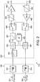
- Referring to
Fig 2 electro-optical transduction devices remote units 310 create in thefibres antennas 400 in the transmit direction, again without frequency conversion. - The
transducer devices - In this embodiment:-
Intermediate chain amplifiers (i.e. in the hub and module RF path) have a wide bandwidth (3dB gain bandwidth 2.7GHz) and a higher linearity [average OIP2 of 50dBm. OIP2 is the theoretical output level at which the second-order two-tone distortion products are equal in power to the desired signals. - A linear DFB laser achieves an OIP2 of 30dBm when using a factory-calibrated input bias current rather than a fixed value.
- A filter in the remote unit attenuates 2nd order components above 2.7GHz (i.e. those coming from carrier signals above 1.35GHz). This allows the amplifier performance above 1.35GHz to be 3rd order limited rather than 2nd order (3rd order limits typically allow a 6dB lower back-off than 2nd order);
- The power amplifier pre-driver has an average OIP2 of 60dBm below 1.35GHz; and
- The power amplifier is a twin transistor high-linearity design which achieves an OIP2 of 70dBm.
- As is well-known, multimode fibres are specified by a frequency-length product "bandwidth" parameter, usually for an over-filled launch (OFL). Transmission may be carried out in improved fashion, improving on the apparent limitation shown by this parameter by using, instead of an overfilled launch, a restricted-mode launch, intended to avoid high-order modes. In this way, baseband digital signals can be carried at higher repetition rates or for longer distances than the bandwidth parameter predicts. The present inventors have also discovered that there is a useable performance region that extends above the accepted frequency limit which may be accessed by a correct choice of excitation modes. This region, if launch conditions are correct, can be generally without zeroes or lossy regions.
- Launch may be either axis-parallel but offset, angularly offset, or any other launch that provides suppression of low and high order modes. For certain multimode fibres, a centre launch works. In one installation technique for mmf, a centre launch is used as an initial attempt then changing to offset launch if there are critical gain nulls.
- In an embodiment of the
remote unit 310, starting with the uplink path, there is anoptical module 180 that consists of aphotodiode 350, with optical connectors for thedownlink fibre 501, and electronics (not shown) for transduction of the optical signal to a desired electrical signal, and alaser 370 having a launch to enable connection of theuplink fibre 502, together with the necessary drive electronics (not shown) for the laser). - The
photodiode 350 is coupled to receive light from theincoming fibre 501 and provides an electrical output at a node 351. Signals at the electrical node 351 correspond directly to variations in the light on the fibre 501.The electrical node 351 forms an input to the electronics 315 of the remote unit. The electronics 315 has a power detector 352 whose output connects to afilter 353 having a low pass output 354 to adigital controller 355. Ahigh pass output 356 of thefilter 353 feeds to aslope compensator 357, and the output of theslope compensator 357 feeds via aswitch 358 and acontrollable attenuator 359 to a high linearity power amplifier 360 (with no filtering within the wide band of operation) having anoutput 361 for driving the transmit antenna (not shown). Controllable attenuator 359 allows for different optical link lengths and types with different amounts of loss together with output level control. This is used in conjunction with theslope compensator 357 which flattens the gain profile of these different optical links as described below. 362 is another variable attenuator that is used for varying the system sensitivity (zero attenuation = high sensitivity but more susceptible to interference, high attenuation = low sensitivity but high interference protection).- In some embodiments there is also an AGC detector (not shown) which allows it to be used for adaptive interference protection. This is useful in a wideband system where they may be many uplink radio sources in a building that are in-band for the DAS but not relevant to the connected base-stations or repeaters.
- The power detector 352 on the uplink from the hub is used to measure fibre loss from the Hub to the remote unit). The filter 352 allows extraction of and insertion of a low frequency, out of band, communications channel for allows the hub and remote unit to communicate.
- In the downlink side of this embodiment, an
input 362 from the receive antenna provides RF signals to the input of acontrollable attenuator 363. The attenuator has an output node 364 coupled to alow noise amplifier 365, and this in turn has an output coupled via aswitch 366 to afilter circuit 367. The output of thefilter circuit 367 is connected via suitable drive circuitry (not shown) to alaser 370, here a DFB laser. The optical output of thelaser 370 is connected to launch light into thedownlink fibre 502. - Signals from the
controller 355 may be conveyed via thefilter 367 and thedownlink fibre 502 back to the hub. - Each fibre run has an absolute loss, which will vary by medium and length as well as a gain slope with frequency, such that higher frequencies (e.g. 2.7 GHz) are attenuated more than lower frequencies (e.g. 200 MHz). The gain slope can be as much as 18 dB across the band of operation. In coax-type embodiments the gain slope may be up to 23dB. It is desirable to achieve an approximately flat frequency response between the hub and all remote units, otherwise accurately controlling the absolute and relative power levels of services at different frequencies and different remote units becomes impossible (as once services are combined, they cannot be uncombined and level shifted in a broadband RF system). Thus each interconnection is slope and gain compensated, so that the relative power levels of all services are independent of length and cable type. This is achieved by the
slope compensator 357, and a counterpart slope compensator for the uplink path. In the embodiment the compensators each have plural selectable frequency vs gain characteristics programmed into them, so that thecontroller 355 may select a characteristic that substantially compensates for the characteristics of the fibre concerned. - The characteristic is selected during a set-up procedure. In an example of this, a signal generator in a hub connected to the fibres 501,502 is controlled to provide a signal at a desired first in-band frequency at a given power level to the
downlink fibre 501, and thence to the power detector 352. The detected power level is transferred to thecontroller 355. Then a different second in-band frequency is output over thedownlink fibre 501, and the relevant power detected, and the value supplied to thecontroller 355. This is repeated over different frequencies to obtain information on the frequency characteristics of thefibre 355. Thecontroller 355 in this embodiment sends back the information on power levels over theuplink fibre 502 to the hub, where the selection of the best-fit compensation characteristic is made. Then a command signal is sent out overdownlink fibre 501, this being passed to thecontroller 355, which has outputs for commanding the compensator 357 to select the relevant best-fit curve. - By use of the loop-back switches, the signal generator in the hub can then be used to compensate for the frequency characteristics of the uplink fibre in a like fashion. In other embodiments, the
controller 355 is programmed to set the characteristics of the associatedcompensator 357 based upon the measurements it makes, without further commands from the hub. In other embodiments, a signal generator may be provided in the remote unit as well as in the hub. Alternatively a signal generator may be temporarily connected as required as part of a commissioning process. - In this embodiment, the fibre is a multimode fibre, and the
laser 370 is coupled to it via a single mode patch cord to provide coaxial but spatially offset launch of light into thefibre 502. - The
switch 358 on the uplink, together with theswitch 366 on the downlink side provides loop-back functionality to allow signals from the hub to be switched back to the hub to allow the hub to perform an RF loop-back measurement. This is from the hub to the remote unit back to the hub to measure cable/fibre loss over frequency. Thecontrollable attenuator 359 in the downlink path, and thecontrollable attenuator 363 in the uplink path allow respectively for output power control and input signal level control. Two slope compensator modules are required in the system per remote unit. In this embodiment the one 357 in the uplink is provided at theRU 311 and that 363 in the downlink is provided in the hub. They are operated to compensate for frequency-dependent loss in the transmission channel, typically in thefibre 501. - The antenna typically consists of active elements and passive elements. The active elements are the antennas, and have conductive connections for signals. The passive elements are not conductively connected to allow signal input or output, and are referred to hereinafter as "stubs".
- Referring to
Fig 3 , a first example of anantenna module 1 has two wide-band printedmonopole antennas circuit board 20. ThePCB 20 stands up orthogonally to acommon ground plane 21. The ground plane has a width dimension and a length dimension with the length dimension being larger than the width dimension. The antenna arrangement is arranged to provide the required isolation- typically 40 dB across the frequency range of the system. This antenna provides a single PCB solution, packaged as a single antenna module, in which the isolation is inherent in the design rather than the positioning of the antenna. - In this example, the antenna module is remote from the electronics which drives it. In another it is integral with a broadband power transmission amplifier and low-noise receiving amplifier, thus minimising the complexity of installation.
- The two broadband printed
monopole antennas antennas ground plane 21, similar to the antenna width dimension, defined by a second respective side perpendicular to the first and extending in the direction along the PCB corresponding to the long dimension of the ground plane 21). In other examples each antenna can be constructed as a rod, strip or patch. - The height dimension in electrical terms is typically a quarter wavelength at the lowest operational frequency. The height of the
patches board 20. - The
antennas throughs - Each monopole has a respective pair of
first stubs supplementary stubs ground plane 21, and extend from it. Each stub 31-37 has at least a first proximal portion that extends generally parallel to the height dimension. The first stubs 31-34 have a generally inverted "L" shape, with a distal portion extending from a remote end of the proximal portion generally parallel to the length dimension of theground plane 21. The first stubs 31-4 are not bounded by dielectric, and they are relatively narrow. Hence their physical length for an electrical length of approximately a quarter wavelength is greater than the height of the patches. The first stubs are disposed inpairs circuit board 20 longitudinally between thepatch antennas ground plane 21 by an amount equal approximately to the length of the distal portions of the stubs, the arrangement being such that the end of distal portions is approximately aligned with the edge of therespective patch antenna - In general, it is desirable to keep the overall dimensions of the antenna module as small as possible, largely for aesthetic reasons, but also to ensure that it can be used in the greatest possible range of locations. However, there is a limiting factor in smallness, caused by the length in the height dimension of the first stubs 31-34, and the fact that they are not disposed on the central axis of the antenna module. The length of the proximal and distal portions is approximately λ/4, where λ is the wavelength of the lowest frequency band, for example 850-950 MHz.
- To achieve this length, as has already been discussed, the elements are folded horizontal over a portion of their length. The vertical/horizontal ratio is to some extent arbitrary. In the present case it is selected to snugly fit within the profile of a radome that houses the antenna module. However folding the stub element is not without its downsides since the horizontal portion adds capacitance to the stub due to proximity between the horizontal (distal) portion and
ground plane 21. The extra capacitance has an impact on the total physical length of the passive element. - The selection of the location of the first stubs 31-34 is important, since it gives rise to a good cancellation of direct coupling between the antennas. Selection of the location can be achieved by trial and error as it may depend on a number of effects. For one thing, any change in the electrical lengths of the stubs will lead to a phase change which in turn affects the physical positioning of the passive elements. In the described examples, the first stubs 31-34 are mutually identical in dimensions. Different length stubs could be chosen, but this would change their physical positioning to arrive at the same cancellation profile.
- The first stubs as shown all turn outwardly- i.e. their distal portions are directed away from the centre region of the earth plane. However it would also alternatively be possible for some or all to be turned inwards so that the distal portions face each other. Each orientation has a different phase effect and requires different positioning of the first stubs.
- The described example has first stubs 31-34 folded outward which has the advantage of lowering the frequency performance of the
patch antennas - In this example the further stubs 35-37 are coplanar with the
patch antennas PCB 20. In this example, thestubs rectangular stubs patch antennas patch antennas rectangular stub 36, having a height of around double that of the smallrectangular stubs PCB 20 of each stub is around 1/12 of the spacing between thepatch antennas rectangular stub 36 is approx half the length of thefirst stubs rectangular stubs patch antennas first stubs - At the higher frequency bands the coupled power between the
patch antennas patch antennas - At mid range frequencies the
stubs further stub 36 is tending towards resonance at these mid range frequencies to induce isolation between the twoantennas further stubs - At high end frequencies, the small
further stubs antennas first stubs further stub 36 provides some isolation contribution. - In this example, all of the stubs and further stubs 31-37 are electrically bonded to the conducting
ground plane 21. Again, two first stubs per monopole are used, but other numbers are envisaged. - In this example the stubs are symmetrically placed - see
Fig 3 . However in other examples, asymmetry may provide improved results depending on the desired performance conditions. It may be necessary to vary the stub disposition to achieve the desired isolation, since it has been found that the placement of the stubs plays a significant role in the antenna-to-antenna isolation. - In the described example, the dual antenna module is integral with the remote unit, having the broadband transmit power amplifier and low noise amplifier for receiving signal integrated into the dual antenna modules, thus minimising the complexity of installation, and providing the best noise and matching performance. In other examples, the antenna is separate from the remote unit.
- In some examples of a distributed antenna system, transfer of signals from hub to remote unit is via multimode fibre. For instance, respective single laser diodes are used for each uplink fibre and each downlink fibre, thereby providing plural services. It is of course possible to use different lasers for each service, or for different groups of service, if desired. In other examples, other means of signal transfer are used instead -for example dual coaxial cable, one for uplink and one for downlink. Alternatively, single mode fibre could be substituted.
- The architecture of the described system example-using mmf- is entirely applicable to a single mode fibre example. If the
optical module 180, and a corresponding optical module at the hub, are omitted, then conductive links can be used in place of fibres. In one embodiment, an interface module is needed to allow for conductive links to be matched to the conductive links and to carry the required signal levels; however in other examples direct coupling to the conductive -eg coaxial cable- links is possible. Where a coax cable link is provided, it may be used to carry a power supply feed to the remote unit. - Referring to
Fig 4 , another example 100 of the antenna module has two wide band printedmonopole antennas single PCB 20 arranged, with appropriate chokes, to provide the required isolation across the frequency range of the system. This example provides a single PCB solution, which can be packaged as a single antenna module and where the isolation is inherent in the design rather than the positioning of the antenna module. - The two wideband printed monopole antennas are aligned parallel to one another in the same plane, and perpendicular to the ground plane 121 of the
PCB 120. In the present example eachantenna - Both antennas have the same orientation; they are mounted onto an electrically common metallic ground plane, and are separated by less than 2λ. Electrical connection is via respective insulating
feedthroughs - Each monopole has a respective pair of
stubs stubs - The two
antennas stubs - At mid range frequencies the
stubs antenna stubs - At high end frequencies, the isolation is mainly due to the increase in electrical separation between
antennas stubs - In this example, the
stubs - It has been found that for many applications a stub length of around λ/4 provides good results. However stub lengths may be varied and it is not essential that all stubs have identical lengths.
- In the second example the stubs are symmetrically placed. However in other examples, asymmetry may provide improved results depending on the desired performance conditions. It may be necessary to vary the stub disposition to achieve the desired isolation, since it has been found that the placement of the stubs plays a significant role in the antenna-to-antenna isolation. The stubs act as secondary
- radiators so providing secondary coupling paths from stub to stub and stub to antenna. These secondary paths can be arranged to cancel the primary coupling path that would exist between antennas when the stubs are not present.
- In the second example, the ground plane is lengthened by folding it round on itself to increase isolation at lower frequencies. This also necessitates forming a hole in the folded ground plane, so that there is only a single ground plane present under the centre of each monopole.
- In the described examples of the antenna module, it is remote from the electronics which drives it. In others it is integral with a wideband power transmission amplifier and low-noise receiving amplifier, thus minimising the complexity of installation. The described multi-medium architecture provides increased flexibility. In yet other examples, only carrier-modulated signals are carried by the multimode fibre, and digital or baseband signals are carried by a separate antenna feed, for example coaxial cable.
Claims (5)
- An active distributed antenna system DAS having a signal hub (300), transmit media, receive media and distributed antennas,characterised in that the signal hub (300) is configured to receive first signals and to transfer the first signals without frequency conversion to distributed antennas (400) via the transmit media, and to receive second signals (305) that enter the DAS (20) at the antennas (400), the second signals being transferred to the hub (300) via the receive media without frequency conversion, the DAS allowing the transfer of signals across the band extending from 170 MHz to 2.7 GHz.
- A DAS according to claim 1, configured to carry the following frequency ranges
Receive - lower Receive - upper Transmit - lower Transmit - upper 380 450 390 460 880 915 925 960 1710 1785 1805 1880 1920 1980 2110 2170 2400 2470 2400 2470 ∼2500 ∼2700 ∼2500 ∼2700 - A DAS according to claim 1 or 2, having no filters in the frequency range of 170 MHz to 2.7 GHz, whereby any FDD or TDD signals in this range may be conveyed
- A DAS according to any preceding claim having a filter in a remote unit configured to attenuate intermodulation and harmonic emissions above 2.7 GHz.
- A method of operating a distributed antenna system DAS (20), the DAS having a signal hub (300), transmit media, receive media and distributed antennas (400),characterised in that the method comprises:receiving first signals at the hub (300),transferring the first signals without frequency conversion to the distributed antennas (400) via the transmit media,receiving second signals (305) that enter the DAS (20) at the distributed antennas (400),transferring the second signals without frequency conversion from the distributed antennas (400) to the hub (300) via the receive media,the DAS allowing the transfer of signals across the band extending from 170 MHz to 2.7 GHz.
Applications Claiming Priority (4)
| Application Number | Priority Date | Filing Date | Title |
|---|---|---|---|
| GB0802760AGB0802760D0 (en) | 2008-02-14 | 2008-02-14 | Antenna device |
| GB0814363AGB0814363D0 (en) | 2008-08-05 | 2008-08-05 | Signal transmission system |
| PCT/GB2009/000404WO2009101417A1 (en) | 2008-02-14 | 2009-02-12 | Communication system |
| EP09710245.3AEP2245699B1 (en) | 2008-02-14 | 2009-02-12 | Communication system |
Related Parent Applications (3)
| Application Number | Title | Priority Date | Filing Date |
|---|---|---|---|
| EP09710245.3Division | 2009-02-12 | ||
| EP09710245.3ADivisionEP2245699B1 (en) | 2008-02-14 | 2009-02-12 | Communication system |
| EP09710245.3ADivision-IntoEP2245699B1 (en) | 2008-02-14 | 2009-02-12 | Communication system |
Publications (2)
| Publication Number | Publication Date |
|---|---|
| EP2565982A1 EP2565982A1 (en) | 2013-03-06 |
| EP2565982B1true EP2565982B1 (en) | 2019-03-20 |
Family
ID=40548770
Family Applications (3)
| Application Number | Title | Priority Date | Filing Date |
|---|---|---|---|
| EP16184890.8AActiveEP3128608B1 (en) | 2008-02-14 | 2009-02-12 | Communication system |
| EP12194863.2AActiveEP2565982B1 (en) | 2008-02-14 | 2009-02-12 | Communication system |
| EP09710245.3AActiveEP2245699B1 (en) | 2008-02-14 | 2009-02-12 | Communication system |
Family Applications Before (1)
| Application Number | Title | Priority Date | Filing Date |
|---|---|---|---|
| EP16184890.8AActiveEP3128608B1 (en) | 2008-02-14 | 2009-02-12 | Communication system |
Family Applications After (1)
| Application Number | Title | Priority Date | Filing Date |
|---|---|---|---|
| EP09710245.3AActiveEP2245699B1 (en) | 2008-02-14 | 2009-02-12 | Communication system |
Country Status (5)
| Country | Link |
|---|---|
| US (3) | US9960487B2 (en) |
| EP (3) | EP3128608B1 (en) |
| JP (1) | JP2011512740A (en) |
| CN (1) | CN101953023A (en) |
| WO (1) | WO2009101417A1 (en) |
Families Citing this family (32)
| Publication number | Priority date | Publication date | Assignee | Title |
|---|---|---|---|---|
| US10270152B2 (en) | 2010-03-31 | 2019-04-23 | Commscope Technologies Llc | Broadband transceiver and distributed antenna system utilizing same |
| US9160449B2 (en) | 2010-10-13 | 2015-10-13 | Ccs Technology, Inc. | Local power management for remote antenna units in distributed antenna systems |
| US9252874B2 (en) | 2010-10-13 | 2016-02-02 | Ccs Technology, Inc | Power management for remote antenna units in distributed antenna systems |
| EP2643947B1 (en) | 2010-11-24 | 2018-09-19 | Corning Optical Communications LLC | Power distribution module(s) capable of hot connection and/or disconnection for distributed antenna systems, and related power units, components, and methods |
| US11296504B2 (en) | 2010-11-24 | 2022-04-05 | Corning Optical Communications LLC | Power distribution module(s) capable of hot connection and/or disconnection for wireless communication systems, and related power units, components, and methods |
| CA2836133A1 (en)* | 2011-05-17 | 2012-11-22 | 3M Innovative Properties Company | Converged in-building network |
| JP5662247B2 (en) | 2011-05-27 | 2015-01-28 | 株式会社日本自動車部品総合研究所 | Antenna device |
| JP5482969B2 (en)* | 2011-12-16 | 2014-05-07 | 株式会社村田製作所 | Communication terminal device and manufacturing method thereof |
| FR2990591A1 (en)* | 2012-05-14 | 2013-11-15 | Thomson Licensing | METHOD OF MAKING A LINE-SLIT ON A MULTILAYER SUBSTRATE AND MULTI-LAYER PRINTED CIRCUIT COMPRISING AT LEAST ONE LINE-SLIT REALIZED ACCORDING TO SAID METHOD AND USED AS AN INSULATED SLOT OR ANTENNA |
| US9154222B2 (en) | 2012-07-31 | 2015-10-06 | Corning Optical Communications LLC | Cooling system control in distributed antenna systems |
| US8922448B2 (en) | 2012-09-26 | 2014-12-30 | Mediatek Singapore Pte. Ltd. | Communication device and antennas with high isolation characteristics |
| US10257056B2 (en) | 2012-11-28 | 2019-04-09 | Corning Optical Communications LLC | Power management for distributed communication systems, and related components, systems, and methods |
| WO2015013880A1 (en)* | 2013-07-30 | 2015-02-05 | 华为终端有限公司 | Wireless terminal |
| EP3039814B1 (en) | 2013-08-28 | 2018-02-21 | Corning Optical Communications Wireless Ltd. | Power management for distributed communication systems, and related components, systems, and methods |
| TWI543447B (en)* | 2013-09-09 | 2016-07-21 | 鴻海精密工業股份有限公司 | Antenna |
| US9271289B2 (en)* | 2013-10-30 | 2016-02-23 | Andrew Wireless Systems Gmbh | Switching sub-system for distributed antenna systems using time division duplexing |
| WO2015079435A1 (en) | 2013-11-26 | 2015-06-04 | Corning Optical Communications Wireless Ltd. | Selective activation of communications services on power-up of a remote unit(s) in a distributed antenna system (das) based on power consumption |
| US9653861B2 (en) | 2014-09-17 | 2017-05-16 | Corning Optical Communications Wireless Ltd | Interconnection of hardware components |
| US9748654B2 (en)* | 2014-12-16 | 2017-08-29 | Laird Technologies, Inc. | Antenna systems with proximity coupled annular rectangular patches |
| US20160261308A1 (en)* | 2015-03-03 | 2016-09-08 | Nec Laboratories America, Inc. | Architecture for cancelling self interference and enabling full duplex communications |
| US9785175B2 (en)* | 2015-03-27 | 2017-10-10 | Corning Optical Communications Wireless, Ltd. | Combining power from electrically isolated power paths for powering remote units in a distributed antenna system(s) (DASs) |
| WO2016179750A1 (en)* | 2015-05-08 | 2016-11-17 | 京信通信技术(广州)有限公司 | Method and device for controlling gain of relay in active das system, and relay machine |
| CN107181063A (en)* | 2016-03-11 | 2017-09-19 | 华为技术有限公司 | A kind of antenna system and communication equipment |
| FR3065349B1 (en)* | 2017-04-12 | 2019-05-03 | Safran Electronics & Defense | SYSTEM COMPRISING A BAY AND A REPLACEABLE MODULE ONLINE |
| JP6953799B2 (en)* | 2017-05-30 | 2021-10-27 | 株式会社デンソー | Antenna device |
| CN108365320B (en)* | 2018-02-08 | 2020-11-24 | 电子科技大学 | An ultra-wideband low-profile log-periodic monopole endfire antenna |
| US10305432B1 (en)* | 2018-03-09 | 2019-05-28 | Zinwave, Ltd. | Balanced RF amplifier using a common mode choke |
| US10728770B2 (en)* | 2018-05-01 | 2020-07-28 | Tunnel Radio Of America, Inc. | Remotely-controlled distributed antenna system for railroad tunnels employing software defined amplifiers |
| GB2586672B (en) | 2019-02-23 | 2022-10-12 | Zinwave Ltd | Multi-range communication system |
| JP7138701B2 (en)* | 2019-11-20 | 2022-09-16 | ペキン シャオミ モバイル ソフトウェア カンパニー, リミテッド | Antenna, terminal middle frame and terminal |
| CN112825385B (en) | 2019-11-20 | 2022-07-01 | 北京小米移动软件有限公司 | Antenna, terminal middle frame and terminal |
| CA3208127A1 (en)* | 2021-01-12 | 2022-07-21 | Galtronics Usa, Inc. | Ultrawideband hyperflat and mesh grid siso/mimo antenna |
Citations (1)
| Publication number | Priority date | Publication date | Assignee | Title |
|---|---|---|---|---|
| WO2006136811A1 (en)* | 2005-06-23 | 2006-12-28 | Zinwave Limited | Optical transmission system |
Family Cites Families (21)
| Publication number | Priority date | Publication date | Assignee | Title |
|---|---|---|---|---|
| US4347625A (en)* | 1980-06-16 | 1982-08-31 | General Electric Company | Arrangement for cellular operation of a repeater trunking system |
| JPH04332878A (en)* | 1991-05-07 | 1992-11-19 | Toyota Central Res & Dev Lab Inc | Electromagnetic field intensity measuring device |
| US6069587A (en)* | 1998-05-15 | 2000-05-30 | Hughes Electronics Corporation | Multiband millimeterwave reconfigurable antenna using RF mem switches |
| FI990395A7 (en) | 1999-02-24 | 2000-08-25 | Nokia Networks Oy | Equipment for suppressing mutual interference between antennas |
| US6583763B2 (en)* | 1999-04-26 | 2003-06-24 | Andrew Corporation | Antenna structure and installation |
| US6721475B1 (en)* | 2000-12-22 | 2004-04-13 | Cheetah Omni, Llc | Apparatus and method for providing gain equalization |
| US20020191565A1 (en)* | 2001-06-08 | 2002-12-19 | Sanjay Mani | Methods and systems employing receive diversity in distributed cellular antenna applications |
| US6624789B1 (en)* | 2002-04-11 | 2003-09-23 | Nokia Corporation | Method and system for improving isolation in radio-frequency antennas |
| GB2390225A (en)* | 2002-06-28 | 2003-12-31 | Picochip Designs Ltd | Radio transceiver antenna arrangement |
| US6868236B2 (en)* | 2002-07-18 | 2005-03-15 | Terabeam Corporation | Apparatus and method for combining multiple optical beams in a free-space optical communications system |
| US7280848B2 (en)* | 2002-09-30 | 2007-10-09 | Andrew Corporation | Active array antenna and system for beamforming |
| US7096042B2 (en)* | 2003-01-21 | 2006-08-22 | Interdigital Technology Corporation | System and method for increasing cellular system capacity by the use of the same frequency and time slot for both uplink and downlink transmissions |
| US7053843B2 (en)* | 2004-01-20 | 2006-05-30 | Sierra Wireless, Inc. | Multi-band antenna system |
| US7071873B2 (en)* | 2004-04-30 | 2006-07-04 | The United States Of America As Represented By The Secretary Of The Air Force | T/R module for satellite TT and C ground link |
| US7330156B2 (en) | 2004-08-20 | 2008-02-12 | Nokia Corporation | Antenna isolation using grounded microwave elements |
| US7733281B2 (en)* | 2004-09-10 | 2010-06-08 | Broadcom Corporation | Combined satellite and broadband access antennas using common infrastructure |
| US7742000B2 (en)* | 2005-05-31 | 2010-06-22 | Tialinx, Inc. | Control of an integrated beamforming array using near-field-coupled or far-field-coupled commands |
| US7630694B2 (en)* | 2005-07-19 | 2009-12-08 | Samsung Electronics Co., Ltd. | Remote access unit and optical network for bidirectional wireless communication using the same |
| KR100663466B1 (en) | 2005-12-09 | 2007-01-02 | 삼성전자주식회사 | Remote Access Unit and Optical Wireless Network Using the Same |
| GB0602770D0 (en)* | 2006-02-10 | 2006-03-22 | Zinwave Ltd | Optical communication |
| US7848770B2 (en)* | 2006-08-29 | 2010-12-07 | Lgc Wireless, Inc. | Distributed antenna communications system and methods of implementing thereof |
- 2009
- 2009-02-12USUS12/864,846patent/US9960487B2/enactiveActive
- 2009-02-12EPEP16184890.8Apatent/EP3128608B1/enactiveActive
- 2009-02-12CNCN2009801053003Apatent/CN101953023A/enactivePending
- 2009-02-12EPEP12194863.2Apatent/EP2565982B1/enactiveActive
- 2009-02-12JPJP2010546396Apatent/JP2011512740A/enactivePending
- 2009-02-12WOPCT/GB2009/000404patent/WO2009101417A1/enactiveApplication Filing
- 2009-02-12EPEP09710245.3Apatent/EP2245699B1/enactiveActive
- 2018
- 2018-03-13USUS15/920,106patent/US10186770B2/enactiveActive
- 2019
- 2019-01-18USUS16/252,244patent/US20190280378A1/ennot_activeAbandoned
Patent Citations (1)
| Publication number | Priority date | Publication date | Assignee | Title |
|---|---|---|---|---|
| WO2006136811A1 (en)* | 2005-06-23 | 2006-12-28 | Zinwave Limited | Optical transmission system |
Also Published As
| Publication number | Publication date |
|---|---|
| EP2245699A1 (en) | 2010-11-03 |
| US20180219284A1 (en) | 2018-08-02 |
| US20120319916A1 (en) | 2012-12-20 |
| EP2565982A1 (en) | 2013-03-06 |
| US10186770B2 (en) | 2019-01-22 |
| JP2011512740A (en) | 2011-04-21 |
| EP3128608B1 (en) | 2019-04-17 |
| EP3128608A1 (en) | 2017-02-08 |
| US20190280378A1 (en) | 2019-09-12 |
| US9960487B2 (en) | 2018-05-01 |
| EP2245699B1 (en) | 2017-11-15 |
| WO2009101417A1 (en) | 2009-08-20 |
| CN101953023A (en) | 2011-01-19 |
Similar Documents
| Publication | Publication Date | Title |
|---|---|---|
| EP2565982B1 (en) | Communication system | |
| KR100521854B1 (en) | Cellular communications systems | |
| US20250253521A1 (en) | Base station antenna with high performance active antenna system (aas) integrated therein | |
| US5581268A (en) | Method and apparatus for increasing antenna efficiency for hand-held mobile satellite communications terminal | |
| US7084823B2 (en) | Integrated front end antenna | |
| EP1049195B1 (en) | Antenna structure and installation | |
| US10270152B2 (en) | Broadband transceiver and distributed antenna system utilizing same | |
| US12101163B2 (en) | Radio frequency signal boosters serving as outdoor infrastructure in high frequency cellular networks | |
| US20110237299A1 (en) | Gps mast module and mobile radio installation | |
| KR20070112347A (en) | Modular repeater | |
| US20230216188A1 (en) | High-performance mobile communication antenna device | |
| KR102234539B1 (en) | High performance mobile communication transceiver base station antenna apparatus | |
| KR20000016841A (en) | System for trasmitting/receiving a signal having a carrier frequency band for a radio base station | |
| WO2002039541A2 (en) | Distributed antenna systems | |
| WO2001006801A1 (en) | Scalable cellular communications system | |
| US20220059949A1 (en) | Mobile radio antenna for connection to at least one mobile base station | |
| EP4627671A1 (en) | Multiband array antenna and multilayer phase shifter | |
| KR20170038690A (en) | Signal divider including air gap | |
| US20250141479A1 (en) | Device including power amplifier in wireless communication system | |
| KR20240117372A (en) | Low noise amplifier and apparatus including thereof for low loss |
Legal Events
| Date | Code | Title | Description |
|---|---|---|---|
| PUAI | Public reference made under article 153(3) epc to a published international application that has entered the european phase | Free format text:ORIGINAL CODE: 0009012 | |
| AC | Divisional application: reference to earlier application | Ref document number:2245699 Country of ref document:EP Kind code of ref document:P | |
| AK | Designated contracting states | Kind code of ref document:A1 Designated state(s):AT BE BG CH CY CZ DE DK EE ES FI FR GB GR HR HU IE IS IT LI LT LU LV MC MK MT NL NO PL PT RO SE SI SK TR | |
| 17P | Request for examination filed | Effective date:20130823 | |
| RBV | Designated contracting states (corrected) | Designated state(s):AT BE BG CH CY CZ DE DK EE ES FI FR GB GR HR HU IE IS IT LI LT LU LV MC MK MT NL NO PL PT RO SE SI SK TR | |
| 17Q | First examination report despatched | Effective date:20160728 | |
| STAA | Information on the status of an ep patent application or granted ep patent | Free format text:STATUS: EXAMINATION IS IN PROGRESS | |
| GRAP | Despatch of communication of intention to grant a patent | Free format text:ORIGINAL CODE: EPIDOSNIGR1 | |
| STAA | Information on the status of an ep patent application or granted ep patent | Free format text:STATUS: GRANT OF PATENT IS INTENDED | |
| INTG | Intention to grant announced | Effective date:20180530 | |
| RIN1 | Information on inventor provided before grant (corrected) | Inventor name:BELL, ANDREW ROBERT Inventor name:HOWE, GRAHAM RONALD Inventor name:FREEMAN, BENEDICT RUSSELL Inventor name:GEARS, TREVOR Inventor name:BOZ, ZAFER Inventor name:MEZZAROBBA, EMILIANO | |
| GRAJ | Information related to disapproval of communication of intention to grant by the applicant or resumption of examination proceedings by the epo deleted | Free format text:ORIGINAL CODE: EPIDOSDIGR1 | |
| STAA | Information on the status of an ep patent application or granted ep patent | Free format text:STATUS: EXAMINATION IS IN PROGRESS | |
| GRAP | Despatch of communication of intention to grant a patent | Free format text:ORIGINAL CODE: EPIDOSNIGR1 | |
| STAA | Information on the status of an ep patent application or granted ep patent | Free format text:STATUS: GRANT OF PATENT IS INTENDED | |
| INTC | Intention to grant announced (deleted) | ||
| INTG | Intention to grant announced | Effective date:20181016 | |
| GRAS | Grant fee paid | Free format text:ORIGINAL CODE: EPIDOSNIGR3 | |
| GRAA | (expected) grant | Free format text:ORIGINAL CODE: 0009210 | |
| STAA | Information on the status of an ep patent application or granted ep patent | Free format text:STATUS: THE PATENT HAS BEEN GRANTED | |
| AC | Divisional application: reference to earlier application | Ref document number:2245699 Country of ref document:EP Kind code of ref document:P | |
| AK | Designated contracting states | Kind code of ref document:B1 Designated state(s):AT BE BG CH CY CZ DE DK EE ES FI FR GB GR HR HU IE IS IT LI LT LU LV MC MK MT NL NO PL PT RO SE SI SK TR | |
| REG | Reference to a national code | Ref country code:GB Ref legal event code:FG4D | |
| REG | Reference to a national code | Ref country code:CH Ref legal event code:EP | |
| REG | Reference to a national code | Ref country code:DE Ref legal event code:R096 Ref document number:602009057598 Country of ref document:DE | |
| REG | Reference to a national code | Ref country code:AT Ref legal event code:REF Ref document number:1111455 Country of ref document:AT Kind code of ref document:T Effective date:20190415 | |
| REG | Reference to a national code | Ref country code:IE Ref legal event code:FG4D | |
| REG | Reference to a national code | Ref country code:NL Ref legal event code:MP Effective date:20190320 | |
| PG25 | Lapsed in a contracting state [announced via postgrant information from national office to epo] | Ref country code:SE Free format text:LAPSE BECAUSE OF FAILURE TO SUBMIT A TRANSLATION OF THE DESCRIPTION OR TO PAY THE FEE WITHIN THE PRESCRIBED TIME-LIMIT Effective date:20190320 Ref country code:LT Free format text:LAPSE BECAUSE OF FAILURE TO SUBMIT A TRANSLATION OF THE DESCRIPTION OR TO PAY THE FEE WITHIN THE PRESCRIBED TIME-LIMIT Effective date:20190320 Ref country code:NO Free format text:LAPSE BECAUSE OF FAILURE TO SUBMIT A TRANSLATION OF THE DESCRIPTION OR TO PAY THE FEE WITHIN THE PRESCRIBED TIME-LIMIT Effective date:20190620 Ref country code:FI Free format text:LAPSE BECAUSE OF FAILURE TO SUBMIT A TRANSLATION OF THE DESCRIPTION OR TO PAY THE FEE WITHIN THE PRESCRIBED TIME-LIMIT Effective date:20190320 | |
| REG | Reference to a national code | Ref country code:LT Ref legal event code:MG4D | |
| PG25 | Lapsed in a contracting state [announced via postgrant information from national office to epo] | Ref country code:BG Free format text:LAPSE BECAUSE OF FAILURE TO SUBMIT A TRANSLATION OF THE DESCRIPTION OR TO PAY THE FEE WITHIN THE PRESCRIBED TIME-LIMIT Effective date:20190620 Ref country code:LV Free format text:LAPSE BECAUSE OF FAILURE TO SUBMIT A TRANSLATION OF THE DESCRIPTION OR TO PAY THE FEE WITHIN THE PRESCRIBED TIME-LIMIT Effective date:20190320 Ref country code:NL Free format text:LAPSE BECAUSE OF FAILURE TO SUBMIT A TRANSLATION OF THE DESCRIPTION OR TO PAY THE FEE WITHIN THE PRESCRIBED TIME-LIMIT Effective date:20190320 Ref country code:GR Free format text:LAPSE BECAUSE OF FAILURE TO SUBMIT A TRANSLATION OF THE DESCRIPTION OR TO PAY THE FEE WITHIN THE PRESCRIBED TIME-LIMIT Effective date:20190621 Ref country code:HR Free format text:LAPSE BECAUSE OF FAILURE TO SUBMIT A TRANSLATION OF THE DESCRIPTION OR TO PAY THE FEE WITHIN THE PRESCRIBED TIME-LIMIT Effective date:20190320 | |
| REG | Reference to a national code | Ref country code:AT Ref legal event code:MK05 Ref document number:1111455 Country of ref document:AT Kind code of ref document:T Effective date:20190320 | |
| PG25 | Lapsed in a contracting state [announced via postgrant information from national office to epo] | Ref country code:CZ Free format text:LAPSE BECAUSE OF FAILURE TO SUBMIT A TRANSLATION OF THE DESCRIPTION OR TO PAY THE FEE WITHIN THE PRESCRIBED TIME-LIMIT Effective date:20190320 Ref country code:IT Free format text:LAPSE BECAUSE OF FAILURE TO SUBMIT A TRANSLATION OF THE DESCRIPTION OR TO PAY THE FEE WITHIN THE PRESCRIBED TIME-LIMIT Effective date:20190320 Ref country code:RO Free format text:LAPSE BECAUSE OF FAILURE TO SUBMIT A TRANSLATION OF THE DESCRIPTION OR TO PAY THE FEE WITHIN THE PRESCRIBED TIME-LIMIT Effective date:20190320 Ref country code:SK Free format text:LAPSE BECAUSE OF FAILURE TO SUBMIT A TRANSLATION OF THE DESCRIPTION OR TO PAY THE FEE WITHIN THE PRESCRIBED TIME-LIMIT Effective date:20190320 Ref country code:PT Free format text:LAPSE BECAUSE OF FAILURE TO SUBMIT A TRANSLATION OF THE DESCRIPTION OR TO PAY THE FEE WITHIN THE PRESCRIBED TIME-LIMIT Effective date:20190720 Ref country code:EE Free format text:LAPSE BECAUSE OF FAILURE TO SUBMIT A TRANSLATION OF THE DESCRIPTION OR TO PAY THE FEE WITHIN THE PRESCRIBED TIME-LIMIT Effective date:20190320 Ref country code:ES Free format text:LAPSE BECAUSE OF FAILURE TO SUBMIT A TRANSLATION OF THE DESCRIPTION OR TO PAY THE FEE WITHIN THE PRESCRIBED TIME-LIMIT Effective date:20190320 | |
| PG25 | Lapsed in a contracting state [announced via postgrant information from national office to epo] | Ref country code:PL Free format text:LAPSE BECAUSE OF FAILURE TO SUBMIT A TRANSLATION OF THE DESCRIPTION OR TO PAY THE FEE WITHIN THE PRESCRIBED TIME-LIMIT Effective date:20190320 | |
| PG25 | Lapsed in a contracting state [announced via postgrant information from national office to epo] | Ref country code:IS Free format text:LAPSE BECAUSE OF FAILURE TO SUBMIT A TRANSLATION OF THE DESCRIPTION OR TO PAY THE FEE WITHIN THE PRESCRIBED TIME-LIMIT Effective date:20190720 Ref country code:AT Free format text:LAPSE BECAUSE OF FAILURE TO SUBMIT A TRANSLATION OF THE DESCRIPTION OR TO PAY THE FEE WITHIN THE PRESCRIBED TIME-LIMIT Effective date:20190320 | |
| REG | Reference to a national code | Ref country code:DE Ref legal event code:R097 Ref document number:602009057598 Country of ref document:DE | |
| PLBE | No opposition filed within time limit | Free format text:ORIGINAL CODE: 0009261 | |
| STAA | Information on the status of an ep patent application or granted ep patent | Free format text:STATUS: NO OPPOSITION FILED WITHIN TIME LIMIT | |
| PG25 | Lapsed in a contracting state [announced via postgrant information from national office to epo] | Ref country code:DK Free format text:LAPSE BECAUSE OF FAILURE TO SUBMIT A TRANSLATION OF THE DESCRIPTION OR TO PAY THE FEE WITHIN THE PRESCRIBED TIME-LIMIT Effective date:20190320 | |
| 26N | No opposition filed | Effective date:20200102 | |
| PG25 | Lapsed in a contracting state [announced via postgrant information from national office to epo] | Ref country code:SI Free format text:LAPSE BECAUSE OF FAILURE TO SUBMIT A TRANSLATION OF THE DESCRIPTION OR TO PAY THE FEE WITHIN THE PRESCRIBED TIME-LIMIT Effective date:20190320 | |
| PG25 | Lapsed in a contracting state [announced via postgrant information from national office to epo] | Ref country code:TR Free format text:LAPSE BECAUSE OF FAILURE TO SUBMIT A TRANSLATION OF THE DESCRIPTION OR TO PAY THE FEE WITHIN THE PRESCRIBED TIME-LIMIT Effective date:20190320 | |
| REG | Reference to a national code | Ref country code:DE Ref legal event code:R119 Ref document number:602009057598 Country of ref document:DE | |
| REG | Reference to a national code | Ref country code:CH Ref legal event code:PL | |
| REG | Reference to a national code | Ref country code:BE Ref legal event code:MM Effective date:20200229 | |
| PG25 | Lapsed in a contracting state [announced via postgrant information from national office to epo] | Ref country code:LU Free format text:LAPSE BECAUSE OF NON-PAYMENT OF DUE FEES Effective date:20200212 Ref country code:MC Free format text:LAPSE BECAUSE OF FAILURE TO SUBMIT A TRANSLATION OF THE DESCRIPTION OR TO PAY THE FEE WITHIN THE PRESCRIBED TIME-LIMIT Effective date:20190320 | |
| PG25 | Lapsed in a contracting state [announced via postgrant information from national office to epo] | Ref country code:CH Free format text:LAPSE BECAUSE OF NON-PAYMENT OF DUE FEES Effective date:20200229 Ref country code:LI Free format text:LAPSE BECAUSE OF NON-PAYMENT OF DUE FEES Effective date:20200229 | |
| PG25 | Lapsed in a contracting state [announced via postgrant information from national office to epo] | Ref country code:DE Free format text:LAPSE BECAUSE OF NON-PAYMENT OF DUE FEES Effective date:20200901 Ref country code:IE Free format text:LAPSE BECAUSE OF NON-PAYMENT OF DUE FEES Effective date:20200212 Ref country code:FR Free format text:LAPSE BECAUSE OF NON-PAYMENT OF DUE FEES Effective date:20200229 | |
| PG25 | Lapsed in a contracting state [announced via postgrant information from national office to epo] | Ref country code:BE Free format text:LAPSE BECAUSE OF NON-PAYMENT OF DUE FEES Effective date:20200229 | |
| PG25 | Lapsed in a contracting state [announced via postgrant information from national office to epo] | Ref country code:MT Free format text:LAPSE BECAUSE OF FAILURE TO SUBMIT A TRANSLATION OF THE DESCRIPTION OR TO PAY THE FEE WITHIN THE PRESCRIBED TIME-LIMIT Effective date:20190320 Ref country code:CY Free format text:LAPSE BECAUSE OF FAILURE TO SUBMIT A TRANSLATION OF THE DESCRIPTION OR TO PAY THE FEE WITHIN THE PRESCRIBED TIME-LIMIT Effective date:20190320 | |
| PG25 | Lapsed in a contracting state [announced via postgrant information from national office to epo] | Ref country code:MK Free format text:LAPSE BECAUSE OF FAILURE TO SUBMIT A TRANSLATION OF THE DESCRIPTION OR TO PAY THE FEE WITHIN THE PRESCRIBED TIME-LIMIT Effective date:20190320 | |
| P01 | Opt-out of the competence of the unified patent court (upc) registered | Effective date:20230601 | |
| REG | Reference to a national code | Ref country code:GB Ref legal event code:732E Free format text:REGISTERED BETWEEN 20230629 AND 20230705 | |
| PGFP | Annual fee paid to national office [announced via postgrant information from national office to epo] | Ref country code:GB Payment date:20250227 Year of fee payment:17 |