EP2543138B1 - Planar audio amplifier output inductor with current sense - Google Patents
Planar audio amplifier output inductor with current senseDownload PDFInfo
- Publication number
- EP2543138B1 EP2543138B1EP11704166.5AEP11704166AEP2543138B1EP 2543138 B1EP2543138 B1EP 2543138B1EP 11704166 AEP11704166 AEP 11704166AEP 2543138 B1EP2543138 B1EP 2543138B1
- Authority
- EP
- European Patent Office
- Prior art keywords
- windings
- inductor
- audio amplifier
- output
- layers
- Prior art date
- Legal status (The legal status is an assumption and is not a legal conclusion. Google has not performed a legal analysis and makes no representation as to the accuracy of the status listed.)
- Active
Links
Images


Classifications
- H—ELECTRICITY
- H03—ELECTRONIC CIRCUITRY
- H03F—AMPLIFIERS
- H03F3/00—Amplifiers with only discharge tubes or only semiconductor devices as amplifying elements
- H03F3/20—Power amplifiers, e.g. Class B amplifiers, Class C amplifiers
- H03F3/21—Power amplifiers, e.g. Class B amplifiers, Class C amplifiers with semiconductor devices only
- H03F3/217—Class D power amplifiers; Switching amplifiers
- H—ELECTRICITY
- H01—ELECTRIC ELEMENTS
- H01F—MAGNETS; INDUCTANCES; TRANSFORMERS; SELECTION OF MATERIALS FOR THEIR MAGNETIC PROPERTIES
- H01F19/00—Fixed transformers or mutual inductances of the signal type
- H01F19/02—Audio-frequency transformers or mutual inductances, i.e. not suitable for handling frequencies considerably beyond the audio range
- H—ELECTRICITY
- H03—ELECTRONIC CIRCUITRY
- H03F—AMPLIFIERS
- H03F1/00—Details of amplifiers with only discharge tubes, only semiconductor devices or only unspecified devices as amplifying elements
- H03F1/56—Modifications of input or output impedances, not otherwise provided for
- H03F1/565—Modifications of input or output impedances, not otherwise provided for using inductive elements
- H—ELECTRICITY
- H01—ELECTRIC ELEMENTS
- H01F—MAGNETS; INDUCTANCES; TRANSFORMERS; SELECTION OF MATERIALS FOR THEIR MAGNETIC PROPERTIES
- H01F3/00—Cores, Yokes, or armatures
- H01F3/10—Composite arrangements of magnetic circuits
- H01F2003/106—Magnetic circuits using combinations of different magnetic materials
Definitions
- an audio amplifierin one aspect, includes a planar inductor structure that includes a first plurality of windings, formed on layers of a first circuit board and a second plurality of windings, formed on layers of a second circuit board.
- the audiomay further include an output stage and a switching stage.
- the first plurality of windingsmay be adjacent the output stage and the second plurality of windings may be adjacent the switching stage.
- the first plurality of windingsmay be separated from the second plurality of windings by a spacing structure having a thickness.
- An inductive coupling constant Kmay be proportional to the thickness.
- the spacing structuremay include layers of dielectric material.
- the spacing structuremay include interconnect pins.
- the first plurality of windings and the second plurality of windingsmay be characterized by a coupling constant K, which may be proportional to the thickness of the spacing structure.
- the planar output inductormay further includes a ferrite core structure substantially enclosing the first plurality of windings and the second plurality of windings.
- the ferrite coremay include two opposing faces separated by a gap having a width.
- the inductance of the output inductormay be proportional to the width of the gap.
- the audio amplifier of claimmay further include a first core structure, including ferrite and a second core structure, includes a material having a magnetic permeability ⁇ in the range of 4 to 200.
- the first structure and the second structuremay be configured so that they form a combined structure having cavities that accommodate the first plurality and the second plurality of windings, wherein the inductance of the output inductor is proportional to ⁇ .
- the audio amplifiermay further include a sense coil, sensing the current in the inductor, formed on a layer of the first circuit board, adjacent one of the first plurality of windings.
- an audio amplifierin another aspect, includes a planar inductor structure that includes a first plurality windings formed on layers of a first circuit board and a sense coil, sensing the current in the first plurality of windings, adjacent the one of the first plurality of windings.
- the planar inductor structuremay further include a second plurality of windings, formed on layers of a second circuit board.
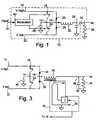
- Figs. 1 , 2 , 3 , and 4Aare block diagrams of class D amplifiers
- Fig. 4Bis a block diagram of a class D amplifier illustrating the effect of coupling capacitance
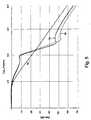
- Fig. 5is a plot of V out V in showing the effect of the a coupling coefficient
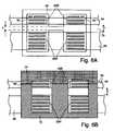
- Figs. 6A and 6Bare diagrammatic cross-sections of planar inductors with current sensing loops.
- Fig. 7is a top plan view of an inductor and a sense coil..
- circuitrymay be referred to as "circuitry", unless otherwise indicated, the elements may be implemented as one of, or a combination of, analog circuitry, digital circuitry, or one or more microprocessors executing software instructions.
- the software instructionsmay include digital signal processing (DSP) instructions. Operations may be performed by analog circuitry or by a microprocessor executing software that performs the mathematical or logical equivalent to the analog operation.
- DSPdigital signal processing
- Signal linesmay be implemented as discrete analog or digital signal lines, as a single discrete digital signal line with appropriate signal processing to process separate streams of audio signals, or as elements of a wireless communication system.
- each blockmay be performed by one element or by a plurality of elements, and may be separated in time.
- the elements that perform the activities of a blockmay be physically separated.
- audio signals or video signals or bothmay be encoded and transmitted in either digital or analog form; conventional digital-to-analog or analog-to-digital converters may not be shown in the figures.
- Fig. 1shows a class D amplifier 10.
- V high voltage source 12is coupled to switching node 14 by switch 16 and to node 18 by diode 20.
- V low voltage source 22is coupled to switching node 14 by switch 24 and to node 18 by diode 26.
- Switching node 14may be coupled to ground through capacitance 40 (which does not necessarily represent a component capacitor and may be parasitic capacitance, for example from field effect transistors [FETs] that perform the function of the switches 16 and 24 and the diodes 20 and 26) and to node 18.
- Node 18is coupled to node 28 by inductor 30.
- Node 28is coupled to ground by output capacitor 32 and is coupled to output terminal 34.
- Output terminal 34is coupled to load 36.
- Modulator 38is operatively coupled to switches 16 and 24 to control switches 16 and 24.
- the inductor 30 and the capacitor 32form an output filter.
- Switching amplifiersgenerally utilize an output filter to prevent switching frequencies and their harmonics from radiating and causing electromagnetic interference (EMI) with other equipment.
- EMIelectromagnetic interference
- switches 16 and 24are closed and opened by the modulator 38 in accordance with a switching cycle.
- Switch 16is closed connecting the load through inductor 30 to a voltage source (V high ) 12 higher than the highest required load voltage for an interval, at the end of which switch 16 is opened and switch 24 is closed connecting the load through inductor 30 to a voltage source(V low ) 22 lower than the lowest required load voltage for another interval, at which point switch 24 opens and switch 16 is closed again.
- the voltage at the loadwill average to a value between V low and V high in proportion to the relative "on" time of the two switches. That proportion (the "duty cycle") is varied substantially continuously by the modulator with the goal to produce the desired output voltage.
- the inductor current(referenced in the outward direction) will change positively when switch 16 is on and change negatively when switch 24 is on and will average to the output current, with the switching cycle variation termed the "ripple current". For the most part, the ripple current will flow through the output capacitor 32, and the average inductor current will equal the current in the load.
- Fig. 2The amplifier of Fig. 2 includes an outer voltage loop in which the voltage at the output terminal 34 is fed back to a voltage feedback circuit including an voltage loop summer 11 and a voltage loop compensator 13.
- an inner current loopincluding a current sensor 42 that senses the current in the inductor 30, a current loop summer 15, and a current loop compensator 17 operates on the output of the outer voltage loop to stabilize the outer voltage loop.
- This current looppreferably includes a high bandwidth, low noise method to sense the current in the output inductor. For reasons that will be explained later, it may be desirable to place the current sensor 42 at the output stage end of the inductor 30; however, the current sensor may be positioned at any convenient point.
- the current sensor 42 of Fig. 2can be implemented as shown in Fig. 3 .
- the current sensor 42includes a sense winding 50 that is inductively coupled to output inductor 30 and is electrically coupled to output terminals 52 through integrator 53, so that the current in the output inductor 30 can be derived from the output at terminals 52. The derived current can then be provided to the current loop summer 15 of Fig. 2 .
- This current sensoris intended for AC only and is not intended for DC.
- Fig. 4Ashows the output portion of a class D amplifier with an additional feature.
- the amplifier of Fig. 4Aadditionally includes a tuned network 54 (including an inductor 56, a capacitor 58, and a resistance 60, in series) connected to a tap on the output inductor, as shown, for example, as in Fig. 8 of U.S. Pat. 7,432,793 , in which the resistance 60 of Fig. 4A is a parasitic resistance.
- the advantage of the tuned network 54will be explained below in the discussion of Fig. 5 .
- An amplifier with the configuration of Fig. 4Amay have some disadvantages if the tuned network inductor 56 is implemented as a conventional wound magnetic structure.
- Disadvantagesmay include coupling capacitance between the sense winding and the windings of the output inductor 30; difficulty in tuning of the resonant network because the tuning is strongly affected by the magnetic coupling coefficient K between the two parts 30A and 30B of the output inductor 30; extra cost resulting from additional windings, taps, and pins; and mechanical problems and variability associated with multiple windings in an inductor with very different numbers of turns and wire gauge.
- Fig. 4Bis the output portion of the class D amplifier of Fig. 4A , in which an additional capacitor 62 (representing the parasitic coupling capacitance between the sense winding 50 and the output inductor 30), has been added between the outputs of switches 16 and 24 and the input to the integrator in the current sense circuit.
- This coupling capacitanceinjects an error term.
- This error termintegrated by the current sense circuit, results in a term proportional to amplifier output voltage summed into the sensor's output. Insofar as we are relying on the sensor to give a clean image of amplifier output current, this is undesirable.
- V inrepresents the voltage at node 64
- V outrepresents the voltage at output terminal 34
- Fig. 5shows the frequency response of V out V in .
- Curve 66represents the frequency response without tuned network 54.
- Curve 68represents the frequency response with the tuned network 54 and a coupling coefficient K of 0.99.
- Curve 70represents the frequency response with the tuned network 54 and a coupling coefficient K of 0.9. It can be seen that a change of only 10% in the parameter K results in a system response difference of about 6 dB.
- Fig. 6Ashows a cross-section of a planar inductor that provides a very repeatable coupling coefficient K and that reduces the effect of the parasitic capacitance represented by capacitor 62 of Fig. 4B .
- Reference numbers with the prime (') indicatorrepresent the physical implementation of the circuit element with the corresponding reference numbers in the previous figures.
- Inductor part 30A'represents the "noisy" part of the inductor, that is, the part of the inductor that includes the end (the "noisy end") of the inductor adjacent the switches 18 and 24 of previous figures.
- Inductor part 30B'represents the "quiet" part of the inductor, that is, the part of the inductor that includes the end ("the quiet end") of the inductor adjacent the output stage.
- the quiet part 30B' of the inductoris formed on layers of the main printed circuit board (pcb) 64, that is, the part of the printed circuit board on which other components are mounted and within which the interconnections to other circuit elements are formed.
- the noisy part 30A of the inductoris formed on layers of an extra pcb structure 66 which is spaced away from the main pcb 64 by a spacer 70, with a thickness t, for example, of 0.2mm.
- the spacingcan be accomplished by dielectric layers in or on the main pcb 64, with interconnect pins, or in other ways.
- the spacing 70provides a repeatable coupling coefficient K between parts 30A and 30B of the inductor.
- the amount of couplingvaries inversely with the thickness of the spacing 70, and can be tailored for the specific coupling desired.
- the winding 50' that generates the current sense signalis positioned on top of the main pcb 64 and is shielded from the "noisy" part of the inductor by the inductor turns.
- the parasitic capacitance represented by capacitor 62 of Fig. 4Bis less than it would be with conventional configurations.
- the ferrite core 68is described in U.S. Pat. 7,432,793 . In the implementation of Fig. 6A , the inductance of the planar inductor is determined by the distance s between the two facing surfaces of the ferrite core.
- Fig. 6Bshows a cross-section of another implementation of a planar inductor that provides a very repeatable coupling coefficient K and that reduces the effect of the parasitic capacitance represented by capacitor 62 of Fig. 4B .
- the implementation of Fig. 6Bis similar to the structure of Fig. 6A , except that the ferrite core 68 of Fig. 6A is replaced by a core structure having a first portion 72 and a second portion 74.
- the first portion 72is a ferrite structure
- the second portion 74includes a low magnetic permeability material having a magnetic permeability ⁇ in the range of 4 to 200.
- One suitable materialis a class of micron scale iron oxide powders in an insulating matrix available commercially from Micrometals Inc.
- the first portion 72 and the second portion 74are configured so that they can be mated to form a core structure having a cavity that accomodates the noisy inductor part 30A' and the quiet inductor part 30B' and the sense coil 50'.
- the first portion 72 and the second portion 74are further configured so that when mated, the first portion 72 at least partially encloses noisy inductor part 30A' and so that the second portion at least partially encloses quiet inductor part 30B'.
- the first portion 72 and the second portionare mated so that the distance s is zero.
- the inductanceis determined by the magnetic permeability ⁇ of the magnetic material of the second portion 74.
- the first portion 72could include the low magnetic permeability material and the second portion could include the ferrite core.
- Fig. 7is a top plan view of a planar inductor with a sense coil without the ferrite core 68 of Fig. 6A or the core structure 72, 74 of Fig. 6B .
- the reference numbers in Fig. 7refer to like numbered elements in previous figures.
- main pcb 64would be typically be significantly larger relative to the inductor and have many other components mounted on it.
- Interconnect pads 80are for connecting an inductor coil to other circuit elements or to vias to interconnect the inductor coil to inductor coils on other layers of the pcb, in a manner as described in U.S. Pat. 7,432,793 .
- Interconnect pads 82are for connecting the sense coil 50' to other circuit elements.
Landscapes
- Engineering & Computer Science (AREA)
- Power Engineering (AREA)
- Multimedia (AREA)
- Amplifiers (AREA)
- Coils Or Transformers For Communication (AREA)
Description
- This specification describes a planar audio amplifier output inductor with current sense. Reference is made to
U.S. Pat. 7,432,793 . Other art is known fromGB 2250383 DE 102007019110 ,US 6628531 ,GB 2351620 US 7332993 . - In one aspect an audio amplifier, includes a planar inductor structure that includes a first plurality of windings, formed on layers of a first circuit board and a second plurality of windings, formed on layers of a second circuit board. The audio may further include an output stage and a switching stage. The first plurality of windings may be adjacent the output stage and the second plurality of windings may be adjacent the switching stage. The first plurality of windings may be separated from the second plurality of windings by a spacing structure having a thickness. An inductive coupling constant K may be proportional to the thickness. The spacing structure may include layers of dielectric material. The spacing structure may include interconnect pins. The first plurality of windings and the second plurality of windings may be characterized by a coupling constant K, which may be proportional to the thickness of the spacing structure. The planar output inductor may further includes a ferrite core structure substantially enclosing the first plurality of windings and the second plurality of windings. The ferrite core may include two opposing faces separated by a gap having a width. The inductance of the output inductor may be proportional to the width of the gap. The audio amplifier of claim may further include a first core structure, including ferrite and a second core structure, includes a material having a magnetic permeability µ in the range of 4 to 200. The first structure and the second structure may be configured so that they form a combined structure having cavities that accommodate the first plurality and the second plurality of windings, wherein the inductance of the output inductor is proportional to µ. The audio amplifier may further include a sense coil, sensing the current in the inductor, formed on a layer of the first circuit board, adjacent one of the first plurality of windings.
- In another aspect, an audio amplifier, includes a planar inductor structure that includes a first plurality windings formed on layers of a first circuit board and a sense coil, sensing the current in the first plurality of windings, adjacent the one of the first plurality of windings. The planar inductor structure may further include a second plurality of windings, formed on layers of a second circuit board.
- Other features, objects, and advantages will become apparent from the following detailed description, when read in connection with the following drawing, in which:
Figs. 1 ,2 ,3 , and4A are block diagrams of class D amplifiers;Fig. 4B is a block diagram of a class D amplifier illustrating the effect of coupling capacitance;Fig. 5 is a plot of
Figs. 6A and 6B are diagrammatic cross-sections of planar inductors with current sensing loops; andFig. 7 is a top plan view of an inductor and a sense coil..- Though the elements of several views of the drawing may be shown and described as discrete elements in a block diagram and may be referred to as "circuitry", unless otherwise indicated, the elements may be implemented as one of, or a combination of, analog circuitry, digital circuitry, or one or more microprocessors executing software instructions. The software instructions may include digital signal processing (DSP) instructions. Operations may be performed by analog circuitry or by a microprocessor executing software that performs the mathematical or logical equivalent to the analog operation. Unless otherwise indicated, signal lines may be implemented as discrete analog or digital signal lines, as a single discrete digital signal line with appropriate signal processing to process separate streams of audio signals, or as elements of a wireless communication system. Some of the processes may be described in block diagrams. The activities that are performed in each block may be performed by one element or by a plurality of elements, and may be separated in time. The elements that perform the activities of a block may be physically separated. Unless otherwise indicated, audio signals or video signals or both may be encoded and transmitted in either digital or analog form; conventional digital-to-analog or analog-to-digital converters may not be shown in the figures.
Fig. 1 shows aclass D amplifier 10. Vhigh voltage source 12 is coupled to switchingnode 14 byswitch 16 and tonode 18 bydiode 20. Vlow voltage source 22 is coupled to switchingnode 14 byswitch 24 and tonode 18 bydiode 26.Switching node 14 may be coupled to ground through capacitance 40 (which does not necessarily represent a component capacitor and may be parasitic capacitance, for example from field effect transistors [FETs] that perform the function of theswitches diodes 20 and 26) and tonode 18.Node 18 is coupled tonode 28 byinductor 30.Node 28 is coupled to ground byoutput capacitor 32 and is coupled tooutput terminal 34.Output terminal 34 is coupled to load 36. Modulator 38 is operatively coupled toswitches control switches - The
inductor 30 and thecapacitor 32 form an output filter. Switching amplifiers generally utilize an output filter to prevent switching frequencies and their harmonics from radiating and causing electromagnetic interference (EMI) with other equipment. - In
operation switches Switch 16 is closed connecting the load throughinductor 30 to a voltage source (Vhigh) 12 higher than the highest required load voltage for an interval, at the end of whichswitch 16 is opened andswitch 24 is closed connecting the load throughinductor 30 to a voltage source(Vlow) 22 lower than the lowest required load voltage for another interval, at whichpoint switch 24 opens andswitch 16 is closed again. The voltage at the load will average to a value between Vlow and Vhigh in proportion to the relative "on" time of the two switches. That proportion (the "duty cycle") is varied substantially continuously by the modulator with the goal to produce the desired output voltage. The inductor current (referenced in the outward direction) will change positively whenswitch 16 is on and change negatively whenswitch 24 is on and will average to the output current, with the switching cycle variation termed the "ripple current". For the most part, the ripple current will flow through theoutput capacitor 32, and the average inductor current will equal the current in the load. - For a variety of reasons, including mitigating distortion caused by the output
filter including inductor 30 andcapacitor 32, it is desirable to close a feedback loop around the output voltage after the filter at the load. As this filter is a second order system and there exist other delays and contributors to phase lag in the amplifier control system, this requires additional compensation to give a stable system. One way to do this is shown inFig. 2 . The amplifier ofFig. 2 includes an outer voltage loop in which the voltage at theoutput terminal 34 is fed back to a voltage feedback circuit including anvoltage loop summer 11 and avoltage loop compensator 13. In addition an inner current loop, including acurrent sensor 42 that senses the current in theinductor 30, acurrent loop summer 15, and acurrent loop compensator 17 operates on the output of the outer voltage loop to stabilize the outer voltage loop. This current loop preferably includes a high bandwidth, low noise method to sense the current in the output inductor. For reasons that will be explained later, it may be desirable to place thecurrent sensor 42 at the output stage end of theinductor 30; however, the current sensor may be positioned at any convenient point. - One high bandwidth AC current sensor is based on integrating the voltage across the
output inductor 30. Starting with

Therefore, thecurrent sensor 42 ofFig. 2 can be implemented as shown inFig. 3 . Thecurrent sensor 42 includes a sense winding 50 that is inductively coupled tooutput inductor 30 and is electrically coupled tooutput terminals 52 throughintegrator 53, so that the current in theoutput inductor 30 can be derived from the output atterminals 52. The derived current can then be provided to thecurrent loop summer 15 ofFig. 2 . This current sensor is intended for AC only and is not intended for DC. Fig. 4A shows the output portion of a class D amplifier with an additional feature. The amplifier ofFig. 4A additionally includes a tuned network 54 (including aninductor 56, acapacitor 58, and aresistance 60, in series) connected to a tap on the output inductor, as shown, for example, as in Fig. 8 ofU.S. Pat. 7,432,793 , in which theresistance 60 ofFig. 4A is a parasitic resistance. The advantage of the tunednetwork 54 will be explained below in the discussion ofFig. 5 . An amplifier with the configuration ofFig. 4A may have some disadvantages if the tunednetwork inductor 56 is implemented as a conventional wound magnetic structure. Disadvantages may include coupling capacitance between the sense winding and the windings of theoutput inductor 30; difficulty in tuning of the resonant network because the tuning is strongly affected by the magnetic coupling coefficient K between the twoparts output inductor 30; extra cost resulting from additional windings, taps, and pins; and mechanical problems and variability associated with multiple windings in an inductor with very different numbers of turns and wire gauge.- The coupling capacitance problem can be explained with reference to
Fig. 4B , which is the output portion of the class D amplifier ofFig. 4A , in which an additional capacitor 62 (representing the parasitic coupling capacitance between the sense winding 50 and the output inductor 30), has been added between the outputs ofswitches - If the two
parts output inductor 30 are expressed as two inductors coupled by a coupling coefficient K, Vin represents the voltage atnode 64, and Vout represents the voltage atoutput terminal 34, then
Fig. 5 shows the frequency response of
Curve 66 represents the frequency response without tunednetwork 54.Curve 68 represents the frequency response with the tunednetwork 54 and a coupling coefficient K of 0.99.Curve 70 represents the frequency response with the tunednetwork 54 and a coupling coefficient K of 0.9. It can be seen that a change of only 10% in the parameter K results in a system response difference of about 6 dB.Fig. 6A shows a cross-section of a planar inductor that provides a very repeatable coupling coefficient K and that reduces the effect of the parasitic capacitance represented bycapacitor 62 ofFig. 4B . Reference numbers with the prime (') indicator represent the physical implementation of the circuit element with the corresponding reference numbers in the previous figures.Inductor part 30A' represents the "noisy" part of the inductor, that is, the part of the inductor that includes the end (the "noisy end") of the inductor adjacent theswitches Inductor part 30B' represents the "quiet" part of the inductor, that is, the part of the inductor that includes the end ("the quiet end") of the inductor adjacent the output stage. Thequiet part 30B' of the inductor is formed on layers of the main printed circuit board (pcb) 64, that is, the part of the printed circuit board on which other components are mounted and within which the interconnections to other circuit elements are formed. Thenoisy part 30A of the inductor is formed on layers of anextra pcb structure 66 which is spaced away from themain pcb 64 by aspacer 70, with a thickness t, for example, of 0.2mm. The spacing can be accomplished by dielectric layers in or on themain pcb 64, with interconnect pins, or in other ways. The spacing 70 provides a repeatable coupling coefficient K betweenparts spacing 70, and can be tailored for the specific coupling desired. The winding 50' that generates the current sense signal is positioned on top of themain pcb 64 and is shielded from the "noisy" part of the inductor by the inductor turns. The parasitic capacitance represented bycapacitor 62 ofFig. 4B is less than it would be with conventional configurations. Theferrite core 68 is described inU.S. Pat. 7,432,793 . In the implementation ofFig. 6A , the inductance of the planar inductor is determined by the distance s between the two facing surfaces of the ferrite core.Fig. 6B shows a cross-section of another implementation of a planar inductor that provides a very repeatable coupling coefficient K and that reduces the effect of the parasitic capacitance represented bycapacitor 62 ofFig. 4B . The implementation ofFig. 6B is similar to the structure ofFig. 6A , except that theferrite core 68 ofFig. 6A is replaced by a core structure having afirst portion 72 and asecond portion 74. Thefirst portion 72 is a ferrite structure, and thesecond portion 74 includes a low magnetic permeability material having a magnetic permeability µ in the range of 4 to 200. One suitable material is a class of micron scale iron oxide powders in an insulating matrix available commercially from Micrometals Inc. of Anaheim, CA, USA. Thefirst portion 72 and thesecond portion 74 are configured so that they can be mated to form a core structure having a cavity that accomodates thenoisy inductor part 30A' and thequiet inductor part 30B' and the sense coil 50'. Thefirst portion 72 and thesecond portion 74 are further configured so that when mated, thefirst portion 72 at least partially enclosesnoisy inductor part 30A' and so that the second portion at least partially enclosesquiet inductor part 30B'. Thefirst portion 72 and the second portion are mated so that the distances is zero. In the configuration ofFig. 6B , the inductance is determined by the magnetic permeability µ of the magnetic material of thesecond portion 74. Other configurations are possible. For example, thefirst portion 72 could include the low magnetic permeability material and the second portion could include the ferrite core.Fig. 7 is a top plan view of a planar inductor with a sense coil without theferrite core 68 ofFig. 6A or thecore structure Fig. 6B . The reference numbers inFig. 7 refer to like numbered elements in previous figures. In an actual implementation,main pcb 64 would be typically be significantly larger relative to the inductor and have many other components mounted on it.Interconnect pads 80 are for connecting an inductor coil to other circuit elements or to vias to interconnect the inductor coil to inductor coils on other layers of the pcb, in a manner as described inU.S. Pat. 7,432,793 .Interconnect pads 82 are for connecting the sense coil 50' to other circuit elements.- Numerous uses of and departures from the specific apparatus and techniques disclosed herein may be made without departing from the inventive concepts. Consequently, the invention is to be construed as embracing each and every novel feature and novel combination of features disclosed herein and limited only by the scope of the appended claims.


Claims (11)
- An audio amplifier, comprising:a planar inductor structure comprising:a first plurality of windings (30A'), formed on layers of a first circuit board (66);a second plurality of windings (30B'), formed on layers of a second circuit board (64).
- The audio amplifier of claim 1, the audio amplifier further comprising an output stage and a switching stage, wherein the first plurality of windings is adjacent the output stage and the second plurality of windings is adjacent the switching stage.
- The audio amplifier of claim 1, wherein the first plurality of windings are separated from the second plurality of windings by a spacing structure having a thickness and wherein an inductive coupling constant K is proportional to the thickness.
- The audio amplifier of claim 3, wherein the spacing structure comprises layers of dielectric material.
- The audio amplifier of claim 3, wherein the spacing structure comprises interconnect pins.
- The audio amplifier of claim 3, the first plurality of windings and the second plurality of windingscharacterized by a coupling constant K, wherein K is proportional to the thickness of the spacing structure.
- The audio amplifier of claim 1, the planar output inductor further comprising a ferrite core structure substantially enclosing the first plurality of windings and the second plurality of windings comprising two opposing faces separated by a gap having a width, wherein the inductance of the output inductor is proportional to the width of the gap.
- The audio amplifier of claim 1, further comprising:a first core structure, comprising ferrite;a second core structure, comprising a material having a magnetic permeability µ in the range of 4 to 200, the first structure and the second structure configured so that they form a combined structure having cavities that accommodate the first plurality and the second plurality of windings, wherein the inductance of the output inductor is proportional to µ.
- The audio amplifier of claim 1, further comprising:a sense coil, sensing the current in the inductor, formed on a layer of the first circuit board, adjacent one of the first plurality of windings.
- An audio amplifier, comprising:a planar inductor structure comprising a first plurality windings (30B') formed on layers of a first circuit board (64); anda sense coil (50'), sensing the current in the first plurality of windings, adjacent the one of the first plurality of windings.
- The audio amplifier of claim 10, the planar inductor structure further comprising a second plurality of windings, formed on layers of a second circuit board.
Applications Claiming Priority (2)
| Application Number | Priority Date | Filing Date | Title |
|---|---|---|---|
| US12/717,208US8243960B2 (en) | 2010-03-04 | 2010-03-04 | Planar audio amplifier output inductor with current sense |
| PCT/US2011/024675WO2011109158A1 (en) | 2010-03-04 | 2011-02-14 | Planar audio amplifier output inductor with current sense |
Publications (2)
| Publication Number | Publication Date |
|---|---|
| EP2543138A1 EP2543138A1 (en) | 2013-01-09 |
| EP2543138B1true EP2543138B1 (en) | 2013-11-27 |
Family
ID=43920911
Family Applications (1)
| Application Number | Title | Priority Date | Filing Date |
|---|---|---|---|
| EP11704166.5AActiveEP2543138B1 (en) | 2010-03-04 | 2011-02-14 | Planar audio amplifier output inductor with current sense |
Country Status (5)
| Country | Link |
|---|---|
| US (1) | US8243960B2 (en) |
| EP (1) | EP2543138B1 (en) |
| JP (1) | JP5517373B2 (en) |
| CN (1) | CN102792584B (en) |
| WO (1) | WO2011109158A1 (en) |
Families Citing this family (7)
| Publication number | Priority date | Publication date | Assignee | Title |
|---|---|---|---|---|
| CN103430252B (en)* | 2011-04-06 | 2017-03-29 | 株式会社村田制作所 | Laminate-type inductor element and its manufacture method |
| US9054658B2 (en) | 2011-05-13 | 2015-06-09 | Bose Corporation | Power supply with rectifier protection |
| US10541063B2 (en)* | 2015-08-11 | 2020-01-21 | Bel Fuse (Macao Commercial Offshore) Limited | Power inductor |
| KR101952866B1 (en)* | 2017-02-22 | 2019-02-27 | 삼성전기주식회사 | Power inductor, board having the same, and current measurement method using the same |
| KR102827665B1 (en) | 2020-05-18 | 2025-07-02 | 삼성전기주식회사 | Coil component |
| KR102747222B1 (en)* | 2020-05-21 | 2024-12-31 | 삼성전기주식회사 | Coil component |
| DE102022118432A1 (en) | 2022-07-22 | 2024-01-25 | Robert Bosch Gmbh | Tracking amplifier for inductive loads |
Family Cites Families (90)
| Publication number | Priority date | Publication date | Assignee | Title |
|---|---|---|---|---|
| DE2841684A1 (en)* | 1978-09-25 | 1980-04-10 | Bucher Guyer Ag Masch | PRESS, IN PARTICULAR STONE PRESS |
| US4253079A (en)* | 1979-04-11 | 1981-02-24 | Amnon Brosh | Displacement transducers employing printed coil structures |
| US4345116A (en)* | 1980-12-31 | 1982-08-17 | Bell Telephone Laboratories, Incorporated | Dynamic, non-hierarchical arrangement for routing traffic |
| JPH04144212A (en) | 1990-10-05 | 1992-05-18 | Cmk Corp | High frequency transformers and coils using printed wiring boards |
| JPH04243104A (en)* | 1991-01-17 | 1992-08-31 | Murata Mfg Co Ltd | Laminated chip transformer |
| JPH0613108U (en)* | 1992-05-28 | 1994-02-18 | ファン・ピ−タ | Transformer |
| JPH05343245A (en)* | 1992-06-05 | 1993-12-24 | Masaki Esashi | Flat transformer |
| US5319342A (en)* | 1992-12-29 | 1994-06-07 | Kami Electronics Ind. Co., Ltd. | Flat transformer |
| US5672998A (en)* | 1995-08-09 | 1997-09-30 | Harris Corporation | Class D amplifier and method |
| US5852717A (en)* | 1996-11-20 | 1998-12-22 | Shiva Corporation | Performance optimizations for computer networks utilizing HTTP |
| DE29824187U1 (en)* | 1997-07-10 | 2000-10-19 | Melcher Ag, Uster | Multilayer planar inductance |
| JP3147826B2 (en)* | 1997-08-20 | 2001-03-19 | エフ・ディ−・ケイ株式会社 | High frequency sheet type transformer |
| US6415329B1 (en)* | 1998-03-06 | 2002-07-02 | Massachusetts Institute Of Technology | Method and apparatus for improving efficiency of TCP/IP protocol over high delay-bandwidth network |
| US6430618B1 (en)* | 1998-03-13 | 2002-08-06 | Massachusetts Institute Of Technology | Method and apparatus for distributing requests among a plurality of resources |
| US6108703A (en)* | 1998-07-14 | 2000-08-22 | Massachusetts Institute Of Technology | Global hosting system |
| US6275470B1 (en)* | 1999-06-18 | 2001-08-14 | Digital Island, Inc. | On-demand overlay routing for computer-based communication networks |
| FI107421B (en)* | 1999-06-28 | 2001-07-31 | Stonesoft Oy | Connection selection method |
| GB2351620A (en) | 1999-07-01 | 2001-01-03 | Semelab Plc | Triangle wave generator, current sensor, class D power amplifier, anti-hiss circuit and loudspeaker protection circuit |
| US7346695B1 (en)* | 2002-10-28 | 2008-03-18 | F5 Networks, Inc. | System and method for performing application level persistence |
| US6415323B1 (en)* | 1999-09-03 | 2002-07-02 | Fastforward Networks | Proximity-based redirection system for robust and scalable service-node location in an internetwork |
| US6449658B1 (en)* | 1999-11-18 | 2002-09-10 | Quikcat.Com, Inc. | Method and apparatus for accelerating data through communication networks |
| US6754699B2 (en)* | 2000-07-19 | 2004-06-22 | Speedera Networks, Inc. | Content delivery and global traffic management network system |
| US6405252B1 (en)* | 1999-11-22 | 2002-06-11 | Speedera Networks, Inc. | Integrated point of presence server network |
| US6754706B1 (en)* | 1999-12-16 | 2004-06-22 | Speedera Networks, Inc. | Scalable domain name system with persistence and load balancing |
| US6665726B1 (en)* | 2000-01-06 | 2003-12-16 | Akamai Technologies, Inc. | Method and system for fault tolerant media streaming over the internet |
| US6820133B1 (en)* | 2000-02-07 | 2004-11-16 | Netli, Inc. | System and method for high-performance delivery of web content using high-performance communications protocol between the first and second specialized intermediate nodes to optimize a measure of communications performance between the source and the destination |
| US7340532B2 (en)* | 2000-03-10 | 2008-03-04 | Akamai Technologies, Inc. | Load balancing array packet routing system |
| US7020719B1 (en)* | 2000-03-24 | 2006-03-28 | Netli, Inc. | System and method for high-performance delivery of Internet messages by selecting first and second specialized intermediate nodes to optimize a measure of communications performance between the source and the destination |
| US6420953B1 (en)* | 2000-05-19 | 2002-07-16 | Pulse Engineering. Inc. | Multi-layer, multi-functioning printed circuit board |
| US7251688B2 (en)* | 2000-05-26 | 2007-07-31 | Akamai Technologies, Inc. | Method for generating a network map |
| EP1290853A2 (en)* | 2000-05-26 | 2003-03-12 | Akamai Technologies, Inc. | Global load balancing across mirrored data centers |
| US7072979B1 (en)* | 2000-06-28 | 2006-07-04 | Cisco Technology, Inc. | Wide area load balancing of web traffic |
| US7165116B2 (en)* | 2000-07-10 | 2007-01-16 | Netli, Inc. | Method for network discovery using name servers |
| US7484002B2 (en)* | 2000-08-18 | 2009-01-27 | Akamai Technologies, Inc. | Content delivery and global traffic management network system |
| US7346676B1 (en)* | 2000-07-19 | 2008-03-18 | Akamai Technologies, Inc. | Load balancing service |
| US6795823B1 (en)* | 2000-08-31 | 2004-09-21 | Neoris Logistics, Inc. | Centralized system and method for optimally routing and tracking articles |
| US7454500B1 (en)* | 2000-09-26 | 2008-11-18 | Foundry Networks, Inc. | Global server load balancing |
| US6628531B2 (en)* | 2000-12-11 | 2003-09-30 | Pulse Engineering, Inc. | Multi-layer and user-configurable micro-printed circuit board |
| WO2002069608A2 (en)* | 2001-01-16 | 2002-09-06 | Akamai Technologies, Inc. | Using virtual domain name service (dns) zones for enterprise content delivery |
| JP2002223132A (en)* | 2001-01-29 | 2002-08-09 | Niigata Seimitsu Kk | Audio reproduction apparatus and method |
| US7155515B1 (en)* | 2001-02-06 | 2006-12-26 | Microsoft Corporation | Distributed load balancing for single entry-point systems |
| US7003572B1 (en)* | 2001-02-28 | 2006-02-21 | Packeteer, Inc. | System and method for efficiently forwarding client requests from a proxy server in a TCP/IP computing environment |
| US7274658B2 (en)* | 2001-03-01 | 2007-09-25 | Akamai Technologies, Inc. | Optimal route selection in a content delivery network |
| US6982954B2 (en)* | 2001-05-03 | 2006-01-03 | International Business Machines Corporation | Communications bus with redundant signal paths and method for compensating for signal path errors in a communications bus |
| US7480705B2 (en)* | 2001-07-24 | 2009-01-20 | International Business Machines Corporation | Dynamic HTTP load balancing method and apparatus |
| US6880002B2 (en)* | 2001-09-05 | 2005-04-12 | Surgient, Inc. | Virtualized logical server cloud providing non-deterministic allocation of logical attributes of logical servers to physical resources |
| US7475157B1 (en)* | 2001-09-14 | 2009-01-06 | Swsoft Holding, Ltd. | Server load balancing system |
| US7373644B2 (en)* | 2001-10-02 | 2008-05-13 | Level 3 Communications, Llc | Automated server replication |
| CA2410172A1 (en)* | 2001-10-29 | 2003-04-29 | Jose Alejandro Rueda | Content routing architecture for enhanced internet services |
| US6606685B2 (en)* | 2001-11-15 | 2003-08-12 | Bmc Software, Inc. | System and method for intercepting file system writes |
| US7257584B2 (en)* | 2002-03-18 | 2007-08-14 | Surgient, Inc. | Server file management |
| US7454458B2 (en)* | 2002-06-24 | 2008-11-18 | Ntt Docomo, Inc. | Method and system for application load balancing |
| US6914508B2 (en)* | 2002-08-15 | 2005-07-05 | Galaxy Power, Inc. | Simplified transformer design for a switching power supply |
| US7185067B1 (en)* | 2002-08-27 | 2007-02-27 | Cisco Technology, Inc. | Load balancing network access requests |
| US7136922B2 (en)* | 2002-10-15 | 2006-11-14 | Akamai Technologies, Inc. | Method and system for providing on-demand content delivery for an origin server |
| GB0227786D0 (en)* | 2002-11-29 | 2003-01-08 | Ibm | Improved remote copy synchronization in disaster recovery computer systems |
| US7126955B2 (en)* | 2003-01-29 | 2006-10-24 | F5 Networks, Inc. | Architecture for efficient utilization and optimum performance of a network |
| EP1599793B1 (en)* | 2003-02-24 | 2015-10-21 | Oracle International Corporation | System and method for server load balancing and server affinity |
| US7430568B1 (en)* | 2003-02-28 | 2008-09-30 | Sun Microsystems, Inc. | Systems and methods for providing snapshot capabilities in a storage virtualization environment |
| US6927661B2 (en)* | 2003-03-05 | 2005-08-09 | Tdk Innoveta Inc. | Planar transformer and output inductor structure with single planar winding board and two magnetic cores |
| US7308499B2 (en)* | 2003-04-30 | 2007-12-11 | Avaya Technology Corp. | Dynamic load balancing for enterprise IP traffic |
| US7398422B2 (en)* | 2003-06-26 | 2008-07-08 | Hitachi, Ltd. | Method and apparatus for data recovery system using storage based journaling |
| US7436775B2 (en)* | 2003-07-24 | 2008-10-14 | Alcatel Lucent | Software configurable cluster-based router using stock personal computers as cluster nodes |
| US7286476B2 (en)* | 2003-08-01 | 2007-10-23 | F5 Networks, Inc. | Accelerating network performance by striping and parallelization of TCP connections |
| US7325109B1 (en)* | 2003-10-24 | 2008-01-29 | Network Appliance, Inc. | Method and apparatus to mirror data at two separate sites without comparing the data at the two sites |
| US7203796B1 (en)* | 2003-10-24 | 2007-04-10 | Network Appliance, Inc. | Method and apparatus for synchronous data mirroring |
| US7389510B2 (en)* | 2003-11-06 | 2008-06-17 | International Business Machines Corporation | Load balancing of servers in a cluster |
| US7380039B2 (en)* | 2003-12-30 | 2008-05-27 | 3Tera, Inc. | Apparatus, method and system for aggregrating computing resources |
| US7426617B2 (en)* | 2004-02-04 | 2008-09-16 | Network Appliance, Inc. | Method and system for synchronizing volumes in a continuous data protection system |
| US7266656B2 (en)* | 2004-04-28 | 2007-09-04 | International Business Machines Corporation | Minimizing system downtime through intelligent data caching in an appliance-based business continuance architecture |
| US8521687B2 (en)* | 2004-08-03 | 2013-08-27 | International Business Machines Corporation | Apparatus, system, and method for selecting optimal replica sources in a grid computing environment |
| US7840963B2 (en)* | 2004-10-15 | 2010-11-23 | Microsoft Corporation | Marking and utilizing portions of memory state information during a switch between virtual machines to minimize software service interruption |
| US7779410B2 (en)* | 2004-12-17 | 2010-08-17 | Sap Ag | Control interfaces for distributed system applications |
| US7710865B2 (en)* | 2005-02-25 | 2010-05-04 | Cisco Technology, Inc. | Disaster recovery for active-standby data center using route health and BGP |
| US8949364B2 (en)* | 2005-09-15 | 2015-02-03 | Ca, Inc. | Apparatus, method and system for rapid delivery of distributed applications |
| US7432793B2 (en)* | 2005-12-19 | 2008-10-07 | Bose Corporation | Amplifier output filter having planar inductor |
| KR20070074059A (en)* | 2006-01-06 | 2007-07-12 | 삼성전자주식회사 | Magnetic core and inductors and transformers comprising the same |
| US7487383B2 (en)* | 2006-06-29 | 2009-02-03 | Dssdr, Llc | Data transfer and recovery process |
| US7719997B2 (en)* | 2006-12-28 | 2010-05-18 | At&T Corp | System and method for global traffic optimization in a network |
| US20080192960A1 (en)* | 2007-02-09 | 2008-08-14 | Nussbaum Michael B | Hybrid Filter for Audio Switching Amplifier |
| US7332993B1 (en)* | 2007-04-10 | 2008-02-19 | Bose Corporation | Planar transformer having fractional windings |
| US7987467B2 (en)* | 2007-04-13 | 2011-07-26 | International Business Machines Corporation | Scale across in a grid computing environment |
| DE102007019110A1 (en) | 2007-04-23 | 2008-10-30 | Osram Gesellschaft mit beschränkter Haftung | Electronic component |
| WO2008138008A1 (en)* | 2007-05-08 | 2008-11-13 | Riverbed Technology, Inc | A hybrid segment-oriented file server and wan accelerator |
| US8310327B2 (en)* | 2007-06-11 | 2012-11-13 | Moog Limited | Low-profile transformer |
| US20080320482A1 (en)* | 2007-06-20 | 2008-12-25 | Dawson Christopher J | Management of grid computing resources based on service level requirements |
| US8073922B2 (en)* | 2007-07-27 | 2011-12-06 | Twinstrata, Inc | System and method for remote asynchronous data replication |
| TW200908542A (en)* | 2007-08-10 | 2009-02-16 | Richtek Technology Corp | Driving device for electrostatic loudspeaker |
| US7970903B2 (en)* | 2007-08-20 | 2011-06-28 | Hitachi, Ltd. | Storage and server provisioning for virtualized and geographically dispersed data centers |
| US7889041B2 (en)* | 2007-11-05 | 2011-02-15 | Schweitzer Engineering Laboratories, Inc. | Systems and methods for forming an isolated transformer |
- 2010
- 2010-03-04USUS12/717,208patent/US8243960B2/enactiveActive
- 2011
- 2011-02-14EPEP11704166.5Apatent/EP2543138B1/enactiveActive
- 2011-02-14WOPCT/US2011/024675patent/WO2011109158A1/enactiveApplication Filing
- 2011-02-14JPJP2012556088Apatent/JP5517373B2/enactiveActive
- 2011-02-14CNCN201180012280.2Apatent/CN102792584B/enactiveActive
Also Published As
| Publication number | Publication date |
|---|---|
| WO2011109158A1 (en) | 2011-09-09 |
| JP5517373B2 (en) | 2014-06-11 |
| CN102792584A (en) | 2012-11-21 |
| EP2543138A1 (en) | 2013-01-09 |
| US20110215893A1 (en) | 2011-09-08 |
| CN102792584B (en) | 2016-08-17 |
| US8243960B2 (en) | 2012-08-14 |
| JP2013521700A (en) | 2013-06-10 |
Similar Documents
| Publication | Publication Date | Title |
|---|---|---|
| EP2543138B1 (en) | Planar audio amplifier output inductor with current sense | |
| US7554423B2 (en) | Cancellation of inductor winding capacitance | |
| US7403403B2 (en) | Noise suppressor | |
| US20030210110A1 (en) | Filter having parasitic inductance cancellation | |
| US7548137B2 (en) | Generalized cancellation of inductor winding capacitance | |
| WO2005106902A1 (en) | A device and method of non-contact energy transmission | |
| US20190260343A1 (en) | Lc filter | |
| WO2005101626A1 (en) | Noise control circuit | |
| US7116203B2 (en) | Circuit using choke coil and choke coil | |
| US7193869B2 (en) | Noise suppressor | |
| US10998876B2 (en) | Balun | |
| US11005443B2 (en) | Multilayer balun | |
| JPH11154843A (en) | System and method for impedance adjuster | |
| US12266458B2 (en) | Common mode choke | |
| US11088669B2 (en) | Band pass filter | |
| KR101690262B1 (en) | Transformer and power supply apparatus including the same | |
| KR101470815B1 (en) | Magnetic resonance type wireless power transmission apparatus for low voltage | |
| JP2010141643A (en) | Stacked electronic component | |
| JP2006186620A (en) | Line filter | |
| CN101986400A (en) | Integrated inductor based on differential mode and common mode filtering | |
| JP3142060B2 (en) | Noise filter | |
| EP1641138A1 (en) | Signal filling/extraction device | |
| US10911014B2 (en) | Electronic component | |
| JP2012023430A (en) | Signal coupling apparatus for plc | |
| JP3118411B2 (en) | Tuning circuit |
Legal Events
| Date | Code | Title | Description |
|---|---|---|---|
| PUAI | Public reference made under article 153(3) epc to a published international application that has entered the european phase | Free format text:ORIGINAL CODE: 0009012 | |
| 17P | Request for examination filed | Effective date:20120827 | |
| AK | Designated contracting states | Kind code of ref document:A1 Designated state(s):AL AT BE BG CH CY CZ DE DK EE ES FI FR GB GR HR HU IE IS IT LI LT LU LV MC MK MT NL NO PL PT RO RS SE SI SK SM TR | |
| DAX | Request for extension of the european patent (deleted) | ||
| GRAP | Despatch of communication of intention to grant a patent | Free format text:ORIGINAL CODE: EPIDOSNIGR1 | |
| RIC1 | Information provided on ipc code assigned before grant | Ipc:H03F 1/56 20060101ALI20130628BHEP Ipc:H01F 19/02 20060101ALI20130628BHEP Ipc:H03F 3/217 20060101AFI20130628BHEP Ipc:H01F 3/10 20060101ALI20130628BHEP | |
| INTG | Intention to grant announced | Effective date:20130729 | |
| GRAS | Grant fee paid | Free format text:ORIGINAL CODE: EPIDOSNIGR3 | |
| GRAA | (expected) grant | Free format text:ORIGINAL CODE: 0009210 | |
| AK | Designated contracting states | Kind code of ref document:B1 Designated state(s):AL AT BE BG CH CY CZ DE DK EE ES FI FR GB GR HR HU IE IS IT LI LT LU LV MC MK MT NL NO PL PT RO RS SE SI SK SM TR | |
| REG | Reference to a national code | Ref country code:GB Ref legal event code:FG4D | |
| REG | Reference to a national code | Ref country code:CH Ref legal event code:EP | |
| REG | Reference to a national code | Ref country code:AT Ref legal event code:REF Ref document number:643053 Country of ref document:AT Kind code of ref document:T Effective date:20131215 | |
| REG | Reference to a national code | Ref country code:IE Ref legal event code:FG4D | |
| REG | Reference to a national code | Ref country code:DE Ref legal event code:R096 Ref document number:602011003966 Country of ref document:DE Effective date:20140123 | |
| REG | Reference to a national code | Ref country code:NL Ref legal event code:VDEP Effective date:20131127 | |
| REG | Reference to a national code | Ref country code:AT Ref legal event code:MK05 Ref document number:643053 Country of ref document:AT Kind code of ref document:T Effective date:20131127 | |
| REG | Reference to a national code | Ref country code:LT Ref legal event code:MG4D | |
| PG25 | Lapsed in a contracting state [announced via postgrant information from national office to epo] | Ref country code:NO Free format text:LAPSE BECAUSE OF FAILURE TO SUBMIT A TRANSLATION OF THE DESCRIPTION OR TO PAY THE FEE WITHIN THE PRESCRIBED TIME-LIMIT Effective date:20140227 Ref country code:NL Free format text:LAPSE BECAUSE OF FAILURE TO SUBMIT A TRANSLATION OF THE DESCRIPTION OR TO PAY THE FEE WITHIN THE PRESCRIBED TIME-LIMIT Effective date:20131127 Ref country code:FI Free format text:LAPSE BECAUSE OF FAILURE TO SUBMIT A TRANSLATION OF THE DESCRIPTION OR TO PAY THE FEE WITHIN THE PRESCRIBED TIME-LIMIT Effective date:20131127 Ref country code:HR Free format text:LAPSE BECAUSE OF FAILURE TO SUBMIT A TRANSLATION OF THE DESCRIPTION OR TO PAY THE FEE WITHIN THE PRESCRIBED TIME-LIMIT Effective date:20131127 Ref country code:LT Free format text:LAPSE BECAUSE OF FAILURE TO SUBMIT A TRANSLATION OF THE DESCRIPTION OR TO PAY THE FEE WITHIN THE PRESCRIBED TIME-LIMIT Effective date:20131127 Ref country code:IS Free format text:LAPSE BECAUSE OF FAILURE TO SUBMIT A TRANSLATION OF THE DESCRIPTION OR TO PAY THE FEE WITHIN THE PRESCRIBED TIME-LIMIT Effective date:20140327 Ref country code:SE Free format text:LAPSE BECAUSE OF FAILURE TO SUBMIT A TRANSLATION OF THE DESCRIPTION OR TO PAY THE FEE WITHIN THE PRESCRIBED TIME-LIMIT Effective date:20131127 | |
| PG25 | Lapsed in a contracting state [announced via postgrant information from national office to epo] | Ref country code:RS Free format text:LAPSE BECAUSE OF FAILURE TO SUBMIT A TRANSLATION OF THE DESCRIPTION OR TO PAY THE FEE WITHIN THE PRESCRIBED TIME-LIMIT Effective date:20131127 Ref country code:BE Free format text:LAPSE BECAUSE OF FAILURE TO SUBMIT A TRANSLATION OF THE DESCRIPTION OR TO PAY THE FEE WITHIN THE PRESCRIBED TIME-LIMIT Effective date:20131127 Ref country code:LV Free format text:LAPSE BECAUSE OF FAILURE TO SUBMIT A TRANSLATION OF THE DESCRIPTION OR TO PAY THE FEE WITHIN THE PRESCRIBED TIME-LIMIT Effective date:20131127 Ref country code:ES Free format text:LAPSE BECAUSE OF FAILURE TO SUBMIT A TRANSLATION OF THE DESCRIPTION OR TO PAY THE FEE WITHIN THE PRESCRIBED TIME-LIMIT Effective date:20131127 Ref country code:AT Free format text:LAPSE BECAUSE OF FAILURE TO SUBMIT A TRANSLATION OF THE DESCRIPTION OR TO PAY THE FEE WITHIN THE PRESCRIBED TIME-LIMIT Effective date:20131127 Ref country code:CY Free format text:LAPSE BECAUSE OF FAILURE TO SUBMIT A TRANSLATION OF THE DESCRIPTION OR TO PAY THE FEE WITHIN THE PRESCRIBED TIME-LIMIT Effective date:20131127 | |
| PG25 | Lapsed in a contracting state [announced via postgrant information from national office to epo] | Ref country code:PT Free format text:LAPSE BECAUSE OF FAILURE TO SUBMIT A TRANSLATION OF THE DESCRIPTION OR TO PAY THE FEE WITHIN THE PRESCRIBED TIME-LIMIT Effective date:20140327 | |
| PG25 | Lapsed in a contracting state [announced via postgrant information from national office to epo] | Ref country code:EE Free format text:LAPSE BECAUSE OF FAILURE TO SUBMIT A TRANSLATION OF THE DESCRIPTION OR TO PAY THE FEE WITHIN THE PRESCRIBED TIME-LIMIT Effective date:20131127 | |
| REG | Reference to a national code | Ref country code:DE Ref legal event code:R097 Ref document number:602011003966 Country of ref document:DE | |
| PG25 | Lapsed in a contracting state [announced via postgrant information from national office to epo] | Ref country code:PL Free format text:LAPSE BECAUSE OF FAILURE TO SUBMIT A TRANSLATION OF THE DESCRIPTION OR TO PAY THE FEE WITHIN THE PRESCRIBED TIME-LIMIT Effective date:20131127 Ref country code:RO Free format text:LAPSE BECAUSE OF FAILURE TO SUBMIT A TRANSLATION OF THE DESCRIPTION OR TO PAY THE FEE WITHIN THE PRESCRIBED TIME-LIMIT Effective date:20131127 Ref country code:SK Free format text:LAPSE BECAUSE OF FAILURE TO SUBMIT A TRANSLATION OF THE DESCRIPTION OR TO PAY THE FEE WITHIN THE PRESCRIBED TIME-LIMIT Effective date:20131127 Ref country code:CZ Free format text:LAPSE BECAUSE OF FAILURE TO SUBMIT A TRANSLATION OF THE DESCRIPTION OR TO PAY THE FEE WITHIN THE PRESCRIBED TIME-LIMIT Effective date:20131127 | |
| PG25 | Lapsed in a contracting state [announced via postgrant information from national office to epo] | Ref country code:DK Free format text:LAPSE BECAUSE OF FAILURE TO SUBMIT A TRANSLATION OF THE DESCRIPTION OR TO PAY THE FEE WITHIN THE PRESCRIBED TIME-LIMIT Effective date:20131127 Ref country code:MC Free format text:LAPSE BECAUSE OF FAILURE TO SUBMIT A TRANSLATION OF THE DESCRIPTION OR TO PAY THE FEE WITHIN THE PRESCRIBED TIME-LIMIT Effective date:20131127 Ref country code:LU Free format text:LAPSE BECAUSE OF FAILURE TO SUBMIT A TRANSLATION OF THE DESCRIPTION OR TO PAY THE FEE WITHIN THE PRESCRIBED TIME-LIMIT Effective date:20140214 | |
| REG | Reference to a national code | Ref country code:CH Ref legal event code:PL | |
| PLBE | No opposition filed within time limit | Free format text:ORIGINAL CODE: 0009261 | |
| STAA | Information on the status of an ep patent application or granted ep patent | Free format text:STATUS: NO OPPOSITION FILED WITHIN TIME LIMIT | |
| PG25 | Lapsed in a contracting state [announced via postgrant information from national office to epo] | Ref country code:LI Free format text:LAPSE BECAUSE OF NON-PAYMENT OF DUE FEES Effective date:20140228 Ref country code:CH Free format text:LAPSE BECAUSE OF NON-PAYMENT OF DUE FEES Effective date:20140228 | |
| 26N | No opposition filed | Effective date:20140828 | |
| REG | Reference to a national code | Ref country code:IE Ref legal event code:MM4A | |
| REG | Reference to a national code | Ref country code:DE Ref legal event code:R097 Ref document number:602011003966 Country of ref document:DE Effective date:20140828 | |
| PG25 | Lapsed in a contracting state [announced via postgrant information from national office to epo] | Ref country code:IE Free format text:LAPSE BECAUSE OF NON-PAYMENT OF DUE FEES Effective date:20140214 | |
| PG25 | Lapsed in a contracting state [announced via postgrant information from national office to epo] | Ref country code:SI Free format text:LAPSE BECAUSE OF FAILURE TO SUBMIT A TRANSLATION OF THE DESCRIPTION OR TO PAY THE FEE WITHIN THE PRESCRIBED TIME-LIMIT Effective date:20131127 | |
| PG25 | Lapsed in a contracting state [announced via postgrant information from national office to epo] | Ref country code:IT Free format text:LAPSE BECAUSE OF FAILURE TO SUBMIT A TRANSLATION OF THE DESCRIPTION OR TO PAY THE FEE WITHIN THE PRESCRIBED TIME-LIMIT Effective date:20131127 | |
| REG | Reference to a national code | Ref country code:FR Ref legal event code:PLFP Year of fee payment:6 | |
| PG25 | Lapsed in a contracting state [announced via postgrant information from national office to epo] | Ref country code:MT Free format text:LAPSE BECAUSE OF FAILURE TO SUBMIT A TRANSLATION OF THE DESCRIPTION OR TO PAY THE FEE WITHIN THE PRESCRIBED TIME-LIMIT Effective date:20131127 | |
| PG25 | Lapsed in a contracting state [announced via postgrant information from national office to epo] | Ref country code:SM Free format text:LAPSE BECAUSE OF FAILURE TO SUBMIT A TRANSLATION OF THE DESCRIPTION OR TO PAY THE FEE WITHIN THE PRESCRIBED TIME-LIMIT Effective date:20131127 | |
| PG25 | Lapsed in a contracting state [announced via postgrant information from national office to epo] | Ref country code:GR Free format text:LAPSE BECAUSE OF FAILURE TO SUBMIT A TRANSLATION OF THE DESCRIPTION OR TO PAY THE FEE WITHIN THE PRESCRIBED TIME-LIMIT Effective date:20140228 Ref country code:BG Free format text:LAPSE BECAUSE OF FAILURE TO SUBMIT A TRANSLATION OF THE DESCRIPTION OR TO PAY THE FEE WITHIN THE PRESCRIBED TIME-LIMIT Effective date:20131127 | |
| PG25 | Lapsed in a contracting state [announced via postgrant information from national office to epo] | Ref country code:TR Free format text:LAPSE BECAUSE OF FAILURE TO SUBMIT A TRANSLATION OF THE DESCRIPTION OR TO PAY THE FEE WITHIN THE PRESCRIBED TIME-LIMIT Effective date:20131127 Ref country code:HU Free format text:LAPSE BECAUSE OF FAILURE TO SUBMIT A TRANSLATION OF THE DESCRIPTION OR TO PAY THE FEE WITHIN THE PRESCRIBED TIME-LIMIT; INVALID AB INITIO Effective date:20110214 | |
| REG | Reference to a national code | Ref country code:FR Ref legal event code:PLFP Year of fee payment:7 | |
| REG | Reference to a national code | Ref country code:FR Ref legal event code:PLFP Year of fee payment:8 | |
| PG25 | Lapsed in a contracting state [announced via postgrant information from national office to epo] | Ref country code:MK Free format text:LAPSE BECAUSE OF FAILURE TO SUBMIT A TRANSLATION OF THE DESCRIPTION OR TO PAY THE FEE WITHIN THE PRESCRIBED TIME-LIMIT Effective date:20131127 | |
| PG25 | Lapsed in a contracting state [announced via postgrant information from national office to epo] | Ref country code:AL Free format text:LAPSE BECAUSE OF FAILURE TO SUBMIT A TRANSLATION OF THE DESCRIPTION OR TO PAY THE FEE WITHIN THE PRESCRIBED TIME-LIMIT Effective date:20131127 | |
| PGFP | Annual fee paid to national office [announced via postgrant information from national office to epo] | Ref country code:GB Payment date:20190227 Year of fee payment:9 | |
| GBPC | Gb: european patent ceased through non-payment of renewal fee | Effective date:20200214 | |
| PG25 | Lapsed in a contracting state [announced via postgrant information from national office to epo] | Ref country code:GB Free format text:LAPSE BECAUSE OF NON-PAYMENT OF DUE FEES Effective date:20200214 | |
| PGFP | Annual fee paid to national office [announced via postgrant information from national office to epo] | Ref country code:DE Payment date:20250122 Year of fee payment:15 | |
| PGFP | Annual fee paid to national office [announced via postgrant information from national office to epo] | Ref country code:FR Payment date:20250122 Year of fee payment:15 |