EP2541471A1 - Portable device with recessed electrical contacts - Google Patents
Portable device with recessed electrical contactsDownload PDFInfo
- Publication number
- EP2541471A1 EP2541471A1EP11305857AEP11305857AEP2541471A1EP 2541471 A1EP2541471 A1EP 2541471A1EP 11305857 AEP11305857 AEP 11305857AEP 11305857 AEP11305857 AEP 11305857AEP 2541471 A1EP2541471 A1EP 2541471A1
- Authority
- EP
- European Patent Office
- Prior art keywords
- perforations
- module
- portable device
- antenna
- contact pads
- Prior art date
- Legal status (The legal status is an assumption and is not a legal conclusion. Google has not performed a legal analysis and makes no representation as to the accuracy of the status listed.)
- Withdrawn
Links
Images


Classifications
- H—ELECTRICITY
- H01—ELECTRIC ELEMENTS
- H01Q—ANTENNAS, i.e. RADIO AERIALS
- H01Q1/00—Details of, or arrangements associated with, antennas
- H01Q1/12—Supports; Mounting means
- H01Q1/22—Supports; Mounting means by structural association with other equipment or articles
- G—PHYSICS
- G06—COMPUTING OR CALCULATING; COUNTING
- G06K—GRAPHICAL DATA READING; PRESENTATION OF DATA; RECORD CARRIERS; HANDLING RECORD CARRIERS
- G06K19/00—Record carriers for use with machines and with at least a part designed to carry digital markings
- G06K19/06—Record carriers for use with machines and with at least a part designed to carry digital markings characterised by the kind of the digital marking, e.g. shape, nature, code
- G06K19/067—Record carriers with conductive marks, printed circuits or semiconductor circuit elements, e.g. credit or identity cards also with resonating or responding marks without active components
- G06K19/07—Record carriers with conductive marks, printed circuits or semiconductor circuit elements, e.g. credit or identity cards also with resonating or responding marks without active components with integrated circuit chips
- G06K19/077—Constructional details, e.g. mounting of circuits in the carrier
- G06K19/07749—Constructional details, e.g. mounting of circuits in the carrier the record carrier being capable of non-contact communication, e.g. constructional details of the antenna of a non-contact smart card
- G—PHYSICS
- G06—COMPUTING OR CALCULATING; COUNTING
- G06Q—INFORMATION AND COMMUNICATION TECHNOLOGY [ICT] SPECIALLY ADAPTED FOR ADMINISTRATIVE, COMMERCIAL, FINANCIAL, MANAGERIAL OR SUPERVISORY PURPOSES; SYSTEMS OR METHODS SPECIALLY ADAPTED FOR ADMINISTRATIVE, COMMERCIAL, FINANCIAL, MANAGERIAL OR SUPERVISORY PURPOSES, NOT OTHERWISE PROVIDED FOR
- G06Q20/00—Payment architectures, schemes or protocols
- G06Q20/08—Payment architectures
- G06Q20/10—Payment architectures specially adapted for electronic funds transfer [EFT] systems; specially adapted for home banking systems
- G06Q20/105—Payment architectures specially adapted for electronic funds transfer [EFT] systems; specially adapted for home banking systems involving programming of a portable memory device, e.g. IC cards, "electronic purses"
- H—ELECTRICITY
- H01—ELECTRIC ELEMENTS
- H01L—SEMICONDUCTOR DEVICES NOT COVERED BY CLASS H10
- H01L2224/00—Indexing scheme for arrangements for connecting or disconnecting semiconductor or solid-state bodies and methods related thereto as covered by H01L24/00
- H01L2224/01—Means for bonding being attached to, or being formed on, the surface to be connected, e.g. chip-to-package, die-attach, "first-level" interconnects; Manufacturing methods related thereto
- H01L2224/42—Wire connectors; Manufacturing methods related thereto
- H01L2224/44—Structure, shape, material or disposition of the wire connectors prior to the connecting process
- H01L2224/45—Structure, shape, material or disposition of the wire connectors prior to the connecting process of an individual wire connector
- H01L2224/45001—Core members of the connector
- H01L2224/45099—Material
- H01L2224/451—Material with a principal constituent of the material being a metal or a metalloid, e.g. boron (B), silicon (Si), germanium (Ge), arsenic (As), antimony (Sb), tellurium (Te) and polonium (Po), and alloys thereof
- H01L2224/45138—Material with a principal constituent of the material being a metal or a metalloid, e.g. boron (B), silicon (Si), germanium (Ge), arsenic (As), antimony (Sb), tellurium (Te) and polonium (Po), and alloys thereof the principal constituent melting at a temperature of greater than or equal to 950°C and less than 1550°C
- H01L2224/45147—Copper (Cu) as principal constituent
- H—ELECTRICITY
- H01—ELECTRIC ELEMENTS
- H01L—SEMICONDUCTOR DEVICES NOT COVERED BY CLASS H10
- H01L2224/00—Indexing scheme for arrangements for connecting or disconnecting semiconductor or solid-state bodies and methods related thereto as covered by H01L24/00
- H01L2224/01—Means for bonding being attached to, or being formed on, the surface to be connected, e.g. chip-to-package, die-attach, "first-level" interconnects; Manufacturing methods related thereto
- H01L2224/42—Wire connectors; Manufacturing methods related thereto
- H01L2224/47—Structure, shape, material or disposition of the wire connectors after the connecting process
- H01L2224/48—Structure, shape, material or disposition of the wire connectors after the connecting process of an individual wire connector
- H01L2224/4805—Shape
- H01L2224/4809—Loop shape
- H01L2224/48091—Arched
- H—ELECTRICITY
- H01—ELECTRIC ELEMENTS
- H01L—SEMICONDUCTOR DEVICES NOT COVERED BY CLASS H10
- H01L2224/00—Indexing scheme for arrangements for connecting or disconnecting semiconductor or solid-state bodies and methods related thereto as covered by H01L24/00
- H01L2224/01—Means for bonding being attached to, or being formed on, the surface to be connected, e.g. chip-to-package, die-attach, "first-level" interconnects; Manufacturing methods related thereto
- H01L2224/42—Wire connectors; Manufacturing methods related thereto
- H01L2224/47—Structure, shape, material or disposition of the wire connectors after the connecting process
- H01L2224/48—Structure, shape, material or disposition of the wire connectors after the connecting process of an individual wire connector
- H01L2224/481—Disposition
- H01L2224/48151—Connecting between a semiconductor or solid-state body and an item not being a semiconductor or solid-state body, e.g. chip-to-substrate, chip-to-passive
- H01L2224/48221—Connecting between a semiconductor or solid-state body and an item not being a semiconductor or solid-state body, e.g. chip-to-substrate, chip-to-passive the body and the item being stacked
- H01L2224/48225—Connecting between a semiconductor or solid-state body and an item not being a semiconductor or solid-state body, e.g. chip-to-substrate, chip-to-passive the body and the item being stacked the item being non-metallic, e.g. insulating substrate with or without metallisation
- H01L2224/48227—Connecting between a semiconductor or solid-state body and an item not being a semiconductor or solid-state body, e.g. chip-to-substrate, chip-to-passive the body and the item being stacked the item being non-metallic, e.g. insulating substrate with or without metallisation connecting the wire to a bond pad of the item
- H01L2224/48228—Connecting between a semiconductor or solid-state body and an item not being a semiconductor or solid-state body, e.g. chip-to-substrate, chip-to-passive the body and the item being stacked the item being non-metallic, e.g. insulating substrate with or without metallisation connecting the wire to a bond pad of the item the bond pad being disposed in a recess of the surface of the item
- H—ELECTRICITY
- H01—ELECTRIC ELEMENTS
- H01L—SEMICONDUCTOR DEVICES NOT COVERED BY CLASS H10
- H01L2224/00—Indexing scheme for arrangements for connecting or disconnecting semiconductor or solid-state bodies and methods related thereto as covered by H01L24/00
- H01L2224/01—Means for bonding being attached to, or being formed on, the surface to be connected, e.g. chip-to-package, die-attach, "first-level" interconnects; Manufacturing methods related thereto
- H01L2224/42—Wire connectors; Manufacturing methods related thereto
- H01L2224/47—Structure, shape, material or disposition of the wire connectors after the connecting process
- H01L2224/49—Structure, shape, material or disposition of the wire connectors after the connecting process of a plurality of wire connectors
- H01L2224/491—Disposition
- H01L2224/49105—Connecting at different heights
- H01L2224/49109—Connecting at different heights outside the semiconductor or solid-state body
- H—ELECTRICITY
- H10—SEMICONDUCTOR DEVICES; ELECTRIC SOLID-STATE DEVICES NOT OTHERWISE PROVIDED FOR
- H10N—ELECTRIC SOLID-STATE DEVICES NOT OTHERWISE PROVIDED FOR
- H10N10/00—Thermoelectric devices comprising a junction of dissimilar materials, i.e. devices exhibiting Seebeck or Peltier effects
Definitions
- the present inventionrelates to portable devices with an electronic chip and a method of manufacturing such devices.
- a supportreceiving on a rear face an antenna connecting an electronic microcircuit and a face having contact pads extending at least in part to the edge of the face.
- Such devicesare found in particular among electronic tags and contactless, contactless and contactless smart cards provided with an electronic module.
- a standard but not limiting for the present inventionis the so-called ISO 7810 which corresponds to a standard format card 85 mm long, 54 mm wide, and 0.76 mm thick.
- the contactsare defined by the 7816 standard in particular as regards their positioning and extent.
- the patent FR2765010(B1 ) describes a dual interface antenna module as well.
- the antennais disposed at the periphery of the electrical contacts to overcome a screen radiofrequency waves formed by the contact pads and thus improve the radio frequency communication.
- the electromagnetic permeability of the moduleis thus improved.
- the patent application EP 1932104 (A1 ) illustrated in figure 1also discloses an antenna module 11 coupled with a relay antenna in a smart card and having means improving the magnetic permeability. It teaches to place the antenna at the periphery of the contact pads 19 on the rear face opposite to that carrying the contact pads and to place at the periphery and outside the contact pads, a plurality of protuberances 33 extending substantially ranges to the periphery of the module. This arrangement has the effect, besides that of providing electromagnetic permeability, contribute to distribute a bonding pressure of the module in a card body cavity during the module transfer phase.
- the protuberancesmay constitute obstacles and / or wear for certain reader connectors when the card is inserted into the slot of the reader.
- the object of the inventionis to avoid the above disadvantages.
- the present inventionalso aims at a construction of the module allowing a reduction of the realization costs while maintaining the performance of electromagnetic permeability with respect to a radiofrequency communication antenna in particular according to ISO / IEC 14443.
- the principle of the inventionis as much as possible to design contact pads, hollowed electrical tracks or have calibrated perforations up to a maximum on these metal parts outside the standardized areas.
- the inventionrelates to an electronic portable device comprising a support receiving on one side contact pads extending substantially to the edge of the face and connecting an electronic microcircuit;
- the deviceis distinguished in that conductive contact pads comprise a plurality of perforations.
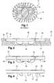
- an electronic portable device 20comprises a support 21 and a face 22 of the support having contact pads 23 extending at least partly to the edge 24 of the face. These ranges are electrically connected to an electronic microcircuit 45.
- the deviceis here in the example a chip card with electrical contacts and the support is an insulating substrate of electronic module 20 for smart card.
- the moduleis embedded in a smart card body.
- the devicemay be the module itself.
- conductive contact padscomprise a plurality of perforations 27.
- the perforationscan be located in zones 25, 26 distinct from the normalized contact areas C1-C8 ( Fig. 5-8 ).
- a plurality of perforationsare for example in the form of round but may have other geometric shapes.
- the total sum of the surfaces thus removedmust be sufficient to allow real savings of materials such as gold, palladium, nickel ... while ensuring sufficient rigidity to comply with the reliability requirements of the products obtained for example micro type module.
- Performationsare performed during the production of the film itself by chemical etching or mechanical cutting together with the contacts.
- Holes 300 ⁇ m in diameterseem to be a good compromise compared to the contact surfaces of the connectors and mechanical resistance to flexion / torsion tests thanks to the rigidity of the module: no effects of walking, no weakening of the electronic part .
- the holesmay preferably be between 250 and 350 ⁇ m in diameter or have an equivalent surface.
- this dimensioncan be variable.
- the modulecan be cut in the copper or in the dielectric support film for the appearance of corrosion. Copper in the latter case is not found in effect exposed on its edge which limits the phenomena of corrosion. However, the space between the edge of the module and the electrical zones may be small enough not to create a stair step effect or for card reader connectors.
- Perforationscan be made anywhere outside the C1-C8 zones defined by ISO 7816 or partially (eg on contact pads but not grounded, or conversely see Fig. 5-8 ); The perforations may be limited on certain areas of the contact areas.
- the moduleis a combi (or dual interface) card module in which the antenna is in a card body as (not shown).
- the modulehere comprises metallizations 28 on both faces 25 and 35. These metallizations may also be perforated.
- the moduleis an antenna module. It receives on a rear face an antenna 29 formed of a set of turns 30 having two connecting ends 31. These ends 31 are connected to the pads of the electronic chip.
- the perforationsform areas of magnetic permeability for the antenna.
- the perforationsmay be arranged at the periphery of the device and / or in the center ( fig.7 );
- the turns of the antennaare arranged substantially at least partly opposite these magnetically permeable zones.
- the perforationsare arranged outside a path (arrow F) of the contact pads of an electrical contact reader connector when the device is introduced into the slot of a reader.
- the perforationsare arranged at the periphery of the device or at the center; the turns are arranged substantially opposite these magnetically permeable zones.
- the inventionmay relate to any form of module where a number 6, 8 of contact pads is necessary.
- Other types of modulecombi plug-in
- single-sided, double-sided type combiantenna module and any new application having a face with electrical contacts.
- Electric contact areasare known in the form of parallelepipeds (see Fig. 5 ), but these can take other forms that still allow a good "supply" of contacts to the connectors.
- the beacheshave their width 46 reduced when approaching an edge 24 at least corresponding to the introduction edge in a reader.
- the edges of the contactsare for example substantially shaped "V". The tip of the V and substantially centered on the path of the connectors when introduced into the reader.
- this "V" shapemakes it possible to clear areas of magnetic permeability 47 between adjacent contact areas of one another.
- the contact padscontain no perforation or a minimum of perforations disposed on the rectilinear path F of the reader connectors which is perpendicular to an edge 24 of the module.
- the connectorsalways slide on substantially solid portions 49 of conductive material, thus avoiding premature wear of connectors and / or contact pads.
- the dielectric substrate 21has a larger area S1 in the upper part S1 and lower S2 of the module.
- the central portion S3 located between the C1-C8 zonesis also free of metal surface.
- the surfaces S1, S2, S3 referred to aboveare provided with portions P1-P5 comprising perforated metal.
- the advantage of these partsis to avoid steps for the connectors but also to promote a good distribution of bonding pressure on the module when fixed in a card body cavity and / or rigidity of the module.
- the devicemay concern a radio frequency token RIFD type, a USB key with or without a radio frequency function, any integrated circuit chip electronic device comprising conductive tracks having a minimum of surface more or less imposed by its function.
- the perforationscan save 20 to 50% of metal relative to the electrical contacts without decreasing their electrical function or mechanical resistance.
- the conductive tracks or connection pads on the back of the modulecan also be perforated.
Landscapes
- Engineering & Computer Science (AREA)
- Computer Hardware Design (AREA)
- Microelectronics & Electronic Packaging (AREA)
- Physics & Mathematics (AREA)
- General Physics & Mathematics (AREA)
- Theoretical Computer Science (AREA)
- Credit Cards Or The Like (AREA)
- Coupling Device And Connection With Printed Circuit (AREA)
- Support Of Aerials (AREA)
- Near-Field Transmission Systems (AREA)
- Multi-Conductor Connections (AREA)
Abstract
Description
Translated fromFrenchLa présente invention concerne des dispositifs portatifs à puce électronique et un procédé de fabrication de tels dispositifs.The present invention relates to portable devices with an electronic chip and a method of manufacturing such devices.
En particulier, elle concerne des dispositifs portables électroniques comportant un support recevant sur une face arrière une antenne reliant un microcircuit électronique et une face comportant des plages de contacts s'étendant au moins en partie jusqu'au bord de la face.In particular, it relates to electronic portable devices comprising a support receiving on a rear face an antenna connecting an electronic microcircuit and a face having contact pads extending at least in part to the edge of the face.
On trouve de tels dispositifs notamment parmi les étiquettes électroniques et les cartes à puce sans-contact, hybrides à contacts et sans-contact pourvues d'un module électronique.Such devices are found in particular among electronic tags and contactless, contactless and contactless smart cards provided with an electronic module.
Une norme usuelle mais nullement limitative pour la présente invention est celle dite ISO 7810 qui correspond à une carte de format standard de 85 mm de longueur, de 54 mm de largeur, et de 0,76 mm d'épaisseur. Les contacts sont définis par la norme 7816 notamment en ce qui concerne leur positionnement et étendue.A standard but not limiting for the present invention is the so-called ISO 7810 which corresponds to a standard format card 85 mm long, 54 mm wide, and 0.76 mm thick. The contacts are defined by the 7816 standard in particular as regards their positioning and extent.
Etat de l'art.State of the art.
On connait la demande de brevet
On connait également le brevet
Le brevet
La demande de brevet
Les protubérances peuvent constituer des obstacles et/ou usures pour certains connecteurs de lecteurs lors de l'introduction de la carte dans la fente du lecteur.The protuberances may constitute obstacles and / or wear for certain reader connectors when the card is inserted into the slot of the reader.
L'invention a pour objectif d'éviter les inconvénients ci-dessus.The object of the invention is to avoid the above disadvantages.
La présente invention vise également une construction du module permettant une réduction des coûts de réalisation tout en conservant les performances de perméabilité électromagnétique par rapport à une antenne de communication radiofréquence notamment selon la norme ISO/IEC 14443.The present invention also aims at a construction of the module allowing a reduction of the realization costs while maintaining the performance of electromagnetic permeability with respect to a radiofrequency communication antenna in particular according to ISO / IEC 14443.
Le principe de l'invention consiste le plus possible à concevoir des plages de contact, pistes électriques évidées ou disposer des perforations calibrées jusqu'à un maximum, sur ces parties métalliques en dehors des zones normalisées.The principle of the invention is as much as possible to design contact pads, hollowed electrical tracks or have calibrated perforations up to a maximum on these metal parts outside the standardized areas.
A cet effet l'invention a pour objet un dispositif portable électronique comportant un support recevant sur une face des plages de contacts s'étendant sensiblement jusqu'au bord de la face et reliant un microcircuit électronique ; Le dispositif se distingue en ce que des plages de contact conductrices comprennent une pluralité de perforations.For this purpose the invention relates to an electronic portable device comprising a support receiving on one side contact pads extending substantially to the edge of the face and connecting an electronic microcircuit; The device is distinguished in that conductive contact pads comprise a plurality of perforations.
Selon d'autres caractéristiques :
- Une face arrière du support comprend une antenne formée d'un ensemble de spires comportant deux extrémités de connexion et en ce que la pluralité de perforations forme des zones de perméabilité magnétique pour l'antenne ;
- Les perforations sont disposées en périphérie du dispositif et/ou au centre, l'antenne étant disposée sensiblement au moins en partie en regard de ces zones magnétiquement perméables ;
- Les perforations sont disposées sur le parcours (F) des plots de contact d'un connecteur de lecteur à contact électrique lorsque le dispositif est introduit dans la fente d'un lecteur ;
- Les plages de contact ont leur largeur réduite vers le bord du support.
- A rear face of the support comprises an antenna formed of a set of turns comprising two ends of connection and in that the plurality of perforations form areas of magnetic permeability for the antenna;
- The perforations are disposed at the periphery of the device and / or in the center, the antenna being disposed substantially at least partly opposite these magnetically permeable zones;
- The perforations are arranged on the path (F) of the contact pads of an electrical contact reader connector when the device is introduced into the slot of a reader;
- The contact pads have their reduced width towards the edge of the support.
Description des figures.Description of the figures.
L'invention sera mieux comprise en se référant à la description suivante faite à titre d'exemple non limitatif et aux dessins ci-annexés, dans lesquels:
- la
figure 1 représente un module pour carte sans contact selon l'état de la technique; - la
figure 2 représente en coupe transversale, un module pour carte à contact selon un mode de réalisation l'invention; - la
figure 3 représente en coupe transversale, un module pour carte hybride sans contact selon un second mode de réalisation de l'invention; - la
figure 4 représente en coupe transversale, un module à antenne pour carte hybride sans-contact selon un second mode de réalisation de l'invention; - les
figures 5A à 5D représentent en vue de dessus des variantes de réalisation des plages de contact d'un module électronique, conformes à l'invention.
- the
figure 1 represents a contactless card module according to the state of the art; - the
figure 2 represents in cross section, a module for contact card according to one embodiment of the invention; - the
figure 3 represents in cross-section, a hybrid card module without contact according to a second embodiment of the invention; - the
figure 4 is a cross-sectional view of a non-contact hybrid card antenna module according to a second embodiment of the invention; - the
Figures 5A to 5D are a top view of variants of the contact pads of an electronic module, according to the invention.
Description détaillée de l'invention.Detailed description of the invention.
Des éléments similaires sont désignés par les mêmes numéros de référence dans l'ensemble des figures.Similar elements are designated by the same reference numerals throughout the figures.
A la
Le dispositif est ici dans l'exemple une carte à puce à contacts électrique et le support est un substrat isolant de module électronique 20 pour carte à puce. Le module est encarté dans un corps 25 de carte à puce. Alternativement, le dispositif peut être le module lui-même.The device is here in the example a chip card with electrical contacts and the support is an insulating substrate of
Selon une caractéristique d'un mode de réalisation, des plages de contact conductrices comprennent une pluralité de perforations 27.According to a feature of one embodiment, conductive contact pads comprise a plurality of
Dans le cas des cartes à puce, les perforations peuvent être localisées dans des zones 25, 26 distinctes des zones de contact normalisées C1-C8 (
Dans l'exemple, une pluralité de perforations sont par exemple sous forme de rond mais peuvent avoir d'autres formes géométriques.In the example, a plurality of perforations are for example in the form of round but may have other geometric shapes.
La somme totale des surfaces ainsi enlevées doit être suffisante pour permettre une réelle économie de matières telles que l'or, palladium, Nickel... tout en assurant une rigidité suffisante pour être conforme aux exigences de fiabilité des produits obtenus par exemple de type micro module.The total sum of the surfaces thus removed must be sufficient to allow real savings of materials such as gold, palladium, nickel ... while ensuring sufficient rigidity to comply with the reliability requirements of the products obtained for example micro type module.
Les performations sont effectuées lors de la fabrication même du film par gravure chimique ou par découpe mécanique en même temps que les contacts.Performations are performed during the production of the film itself by chemical etching or mechanical cutting together with the contacts.
Des trous de 300µm de diamètre semblent être un bon compromis par rapport aux surfaces de contact des connecteurs et une tenue mécanique aux tests de flexion/torsion grâce à la rigidité du module : pas d'effets de marche, pas de fragilisation de la partie électronique. Les trous peuvent être de préférence compris entre 250 et 350 µm de diamètre ou présenter une surface équivalente.Holes 300μm in diameter seem to be a good compromise compared to the contact surfaces of the connectors and mechanical resistance to flexion / torsion tests thanks to the rigidity of the module: no effects of walking, no weakening of the electronic part . The holes may preferably be between 250 and 350 μm in diameter or have an equivalent surface.
Cependant en fonction du modèle voulu et des évolutions technologiques des fournisseurs de substrat de module dit « leadframe » (substrat comprenant ou supportant des plages de contact), cette dimension peut être variable.However, depending on the desired model and the technological developments of the so-called "leadframe" substrate substrate suppliers (substrate comprising or supporting contact pads), this dimension can be variable.
Le module peut être découpé dans le cuivre ou dans le film support diélectrique pour l'aspect corrosion. Le cuivre dans ce dernier cas ne se retrouve pas en effet mis à nu sur sa tranche ce qui limite les phénomènes de corrosion. L'espace entre le bord du module et les zones électriques peuvent être toutefois suffisamment réduit pour ne pas créer d'effet de marche d'escalier ou pour les connecteurs de lecteur de carte.The module can be cut in the copper or in the dielectric support film for the appearance of corrosion. Copper in the latter case is not found in effect exposed on its edge which limits the phenomena of corrosion. However, the space between the edge of the module and the electrical zones may be small enough not to create a stair step effect or for card reader connectors.
Il n'y a pas de risque de fluage de résine (collage de la puce, résine d'encapsulation...) lors de l'assemblage dans la mesure où celle-ci est déposée sur une zone où le diélectrique est plein ou dans le cas contraire (cas d'une fenêtre centrale, zones de soudure), sur une zone où les perforations dans le cuivre sont absentes.There is no risk of resin creep (sticking of the chip, encapsulation resin, etc.) during assembly, insofar as the latter is deposited on an area where the dielectric is solid or in the opposite case (case of a central window, welding zones), on an area where the perforations in the copper are absent.
Les perforations peuvent être faites partout en dehors des zones C1-C8 définies par l'ISO 7816 ou partiellement (ex : sur les plages de contact mais pas à la masse, ou inversement voir
A la
A la
De manière avantageuse, les perforations forment des zones de perméabilité magnétique pour l'antenne.Advantageously, the perforations form areas of magnetic permeability for the antenna.
Les perforations peuvent être disposées en périphérie du dispositif et/ou au centre (
Selon une caractéristique de l'invention, les perforations sont disposées en dehors d'un parcours (flèche F) des plots de contact d'un connecteur de lecteur à contact électrique lorsque le dispositif est introduit dans la fente d'un lecteur.According to one characteristic of the invention, the perforations are arranged outside a path (arrow F) of the contact pads of an electrical contact reader connector when the device is introduced into the slot of a reader.
Les perforations sont disposées en périphérie du dispositif ou au centre ; les spires sont disposées sensiblement en regard de ces zones perméables magnétiquement.The perforations are arranged at the periphery of the device or at the center; the turns are arranged substantially opposite these magnetically permeable zones.
L'invention peut concerner toute forme de module où un nombre 6, 8 de plages de contact est nécessaire. D'autres types de module (combi plug-in), simple face, double face type combi, module antenne et toute nouvelle application ayant une face avec des contacts électriques.The invention may relate to any form of module where a number 6, 8 of contact pads is necessary. Other types of module (combi plug-in), single-sided, double-sided type combi, antenna module and any new application having a face with electrical contacts.
On connait les plages de contact électriques sous forme de parallélépipèdes (voir
En particulier, comme illustré à la
Ainsi, cette forme en « V » permet de dégager des zones de perméabilité magnétique 47 entre de plages de contact adjacentes l'une de l'autre.Thus, this "V" shape makes it possible to clear areas of
Avantageusement, les plages de contact ne contiennent aucune perforation ou un minimum de perforations disposées sur le parcours rectiligne F des connecteurs de lecteur qui est perpendiculaire à un bord 24 du module.Advantageously, the contact pads contain no perforation or a minimum of perforations disposed on the rectilinear path F of the reader connectors which is perpendicular to an
Ainsi, les connecteurs glissent toujours sur des parties sensiblement pleines 49 de matière conductrice, évitant ainsi une usure prématurée de connecteurs et/ou plages de contact.Thus, the connectors always slide on substantially solid portions 49 of conductive material, thus avoiding premature wear of connectors and / or contact pads.
A la
La partie centrale S3 située entre les zones C1- C8 est dépourvue également de surface métallique.The central portion S3 located between the C1-C8 zones is also free of metal surface.
A la
Le dispositif peut concerner un jeton radiofréquence de type RIFD, une clé USB dotée ou non d'une fonction radiofréquence, tout dispositif électronique à puce de circuit intégré comportant des pistes conductrices ayant un minimum de surface plus ou moins imposée par sa fonction. Les perforations permettent de gagner 20 à 50 % de métal relatif aux contacts électriques sans diminuer leur fonction électrique ou résistance mécanique.The device may concern a radio frequency token RIFD type, a USB key with or without a radio frequency function, any integrated circuit chip electronic device comprising conductive tracks having a minimum of surface more or less imposed by its function. The perforations can save 20 to 50% of metal relative to the electrical contacts without decreasing their electrical function or mechanical resistance.
Les pistes conductrices ou plages de connexions à l'arrière du module (
Claims (6)
Translated fromFrenchPriority Applications (7)
| Application Number | Priority Date | Filing Date | Title |
|---|---|---|---|
| EP11305857AEP2541471A1 (en) | 2011-07-01 | 2011-07-01 | Portable device with recessed electrical contacts |
| US14/130,260US9318790B2 (en) | 2011-07-01 | 2012-06-22 | Portable device with apertured electrical contacts |
| JP2014517617AJP5719971B2 (en) | 2011-07-01 | 2012-06-22 | Portable device with perforated electrical terminals |
| KR1020147002575AKR101569301B1 (en) | 2011-07-01 | 2012-06-22 | Portable device with apertured electrical contacts |
| ES12735234TES2938055T3 (en) | 2011-07-01 | 2012-06-22 | Portable device with perforated electrical contacts |
| PCT/EP2012/062153WO2013004522A2 (en) | 2011-07-01 | 2012-06-22 | Portable device with apertured electrical contacts |
| EP12735234.2AEP2727052B1 (en) | 2011-07-01 | 2012-06-22 | Portable device with apertured electrical contacts |
Applications Claiming Priority (1)
| Application Number | Priority Date | Filing Date | Title |
|---|---|---|---|
| EP11305857AEP2541471A1 (en) | 2011-07-01 | 2011-07-01 | Portable device with recessed electrical contacts |
Publications (1)
| Publication Number | Publication Date |
|---|---|
| EP2541471A1true EP2541471A1 (en) | 2013-01-02 |
Family
ID=46513717
Family Applications (2)
| Application Number | Title | Priority Date | Filing Date |
|---|---|---|---|
| EP11305857AWithdrawnEP2541471A1 (en) | 2011-07-01 | 2011-07-01 | Portable device with recessed electrical contacts |
| EP12735234.2AActiveEP2727052B1 (en) | 2011-07-01 | 2012-06-22 | Portable device with apertured electrical contacts |
Family Applications After (1)
| Application Number | Title | Priority Date | Filing Date |
|---|---|---|---|
| EP12735234.2AActiveEP2727052B1 (en) | 2011-07-01 | 2012-06-22 | Portable device with apertured electrical contacts |
Country Status (6)
| Country | Link |
|---|---|
| US (1) | US9318790B2 (en) |
| EP (2) | EP2541471A1 (en) |
| JP (1) | JP5719971B2 (en) |
| KR (1) | KR101569301B1 (en) |
| ES (1) | ES2938055T3 (en) |
| WO (1) | WO2013004522A2 (en) |
Cited By (25)
| Publication number | Priority date | Publication date | Assignee | Title |
|---|---|---|---|---|
| WO2015128188A3 (en)* | 2014-02-27 | 2015-12-23 | Féinics Amatech Teoranta | Rfid transponder chip modules |
| WO2016051092A1 (en)* | 2014-09-30 | 2016-04-07 | Linxens Holding | Chip card manufacturing method, and chip card obtained by said method |
| US9489613B2 (en) | 2011-08-08 | 2016-11-08 | Féinics Amatech Teoranta | RFID transponder chip modules with a band of the antenna extending inward |
| US9622359B2 (en) | 2011-08-08 | 2017-04-11 | Féinics Amatech Teoranta | RFID transponder chip modules |
| US9634391B2 (en) | 2011-08-08 | 2017-04-25 | Féinics Amatech Teoranta | RFID transponder chip modules |
| US9812782B2 (en) | 2011-08-08 | 2017-11-07 | Féinics Amatech Teoranta | Coupling frames for RFID devices |
| WO2017191373A1 (en)* | 2016-05-01 | 2017-11-09 | Smart Packaging Solutions (S.P.S.) | Electronic module of small size for a chip card |
| US10248902B1 (en) | 2017-11-06 | 2019-04-02 | Féinics Amatech Teoranta | Coupling frames for RFID devices |
| US10518518B2 (en) | 2013-01-18 | 2019-12-31 | Féinics Amatech Teoranta | Smart cards with metal layer(s) and methods of manufacture |
| US10552722B2 (en) | 2014-08-10 | 2020-02-04 | Féinics Amatech Teoranta | Smartcard with coupling frame antenna |
| US10599972B2 (en) | 2013-01-18 | 2020-03-24 | Féinics Amatech Teoranta | Smartcard constructions and methods |
| US10733494B2 (en) | 2014-08-10 | 2020-08-04 | Féinics Amatech Teoranta | Contactless metal card constructions |
| US10783426B2 (en) | 2012-08-30 | 2020-09-22 | David Finn | Dual-interface metal hybrid smartcard |
| US10824931B2 (en) | 2012-08-30 | 2020-11-03 | Féinics Amatech Teoranta | Contactless smartcards with multiple coupling frames |
| US10839282B2 (en) | 2014-03-08 | 2020-11-17 | Féinics Amatech Teoranta | RFID transponder chip modules, elements thereof, and methods |
| EP3751464A1 (en) | 2014-02-27 | 2020-12-16 | Féinics Amatech Teoranta | Transponder chip modules and method of making same |
| US10977542B2 (en) | 2013-01-18 | 2021-04-13 | Amtech Group Limited Industrial Estate | Smart cards with metal layer(s) and methods of manufacture |
| USD942538S1 (en) | 2020-07-30 | 2022-02-01 | Federal Card Services, LLC | Asymmetrical arrangement of contact pads and connection bridges of a transponder chip module |
| USD943024S1 (en) | 2020-07-30 | 2022-02-08 | Federal Card Services, LLC | Asymmetrical arrangement of contact pads and connection bridges of a transponder chip module |
| US11341389B2 (en) | 2013-01-18 | 2022-05-24 | Amatech Group Limited | Manufacturing metal inlays for dual interface metal cards |
| US11354560B2 (en) | 2013-01-18 | 2022-06-07 | Amatech Group Limited | Smartcards with multiple coupling frames |
| US11354558B2 (en) | 2013-01-18 | 2022-06-07 | Amatech Group Limited | Contactless smartcards with coupling frames |
| US11551051B2 (en) | 2013-01-18 | 2023-01-10 | Amatech Group Limiied | Coupling frames for smartcards with various module opening shapes |
| US11928537B2 (en) | 2013-01-18 | 2024-03-12 | Amatech Group Limited | Manufacturing metal inlays for dual interface metal cards |
| WO2025022042A1 (en)* | 2023-07-25 | 2025-01-30 | Smart Packaging Solutions | Thick electronic module for a smart card having a metal body |
Families Citing this family (9)
| Publication number | Priority date | Publication date | Assignee | Title |
|---|---|---|---|---|
| US9798968B2 (en) | 2013-01-18 | 2017-10-24 | Féinics Amatech Teoranta | Smartcard with coupling frame and method of increasing activation distance of a transponder chip module |
| US10867235B2 (en) | 2011-08-08 | 2020-12-15 | Féinics Amatech Teoranta | Metallized smartcard constructions and methods |
| US9475086B2 (en) | 2013-01-18 | 2016-10-25 | Féinics Amatech Teoranta | Smartcard with coupling frame and method of increasing activation distance of a transponder chip module |
| USD756317S1 (en) | 2014-08-26 | 2016-05-17 | Féinics Amatech Teoranta | Layout for contact pads and connection bridges of a transponder chip module |
| JPWO2017018039A1 (en)* | 2015-07-30 | 2018-05-17 | ソニー株式会社 | Electric circuit, communication device, and method of manufacturing electric circuit |
| EP3159831B1 (en)* | 2015-10-21 | 2018-10-03 | Nxp B.V. | Dual-interface ic card |
| JP6888402B2 (en)* | 2017-05-01 | 2021-06-16 | 凸版印刷株式会社 | Board module |
| EP3762871B1 (en) | 2018-03-07 | 2024-08-07 | X-Card Holdings, LLC | Metal card |
| EP4371033A1 (en)* | 2021-07-15 | 2024-05-22 | Linxens Holding | Lead-frame, card body of a smart card, smart card, and method of forming a smart card |
Citations (5)
| Publication number | Priority date | Publication date | Assignee | Title |
|---|---|---|---|---|
| FR2765010B1 (en) | 1997-06-20 | 1999-07-16 | Inside Technologies | ELECTRONIC MICROMODULE, ESPECIALLY FOR CHIP CARDS |
| EP1492148A2 (en) | 2003-06-06 | 2004-12-29 | NEC Corporation | Method of manufacturing a high-pressure discharge lamp |
| EP1031939B1 (en) | 1997-11-14 | 2005-09-14 | Toppan Printing Co., Ltd. | Composite ic card |
| EP1932104A1 (en) | 2005-08-30 | 2008-06-18 | Smart Packaging Solutions (SPS) | Double interface communication electronic module, in particular for a chip card |
| US20090271972A1 (en)* | 2005-11-21 | 2009-11-05 | Gemplus | Method for Producing a Contactless Transponder by Stitching a Contactless Module to an Antenna, and Transponder Obtained |
Family Cites Families (4)
| Publication number | Priority date | Publication date | Assignee | Title |
|---|---|---|---|---|
| FR2797976B1 (en)* | 1999-08-25 | 2002-03-22 | Gemplus Card Int | METHOD FOR MANUFACTURING HYBRID CHIP CARDS AND CHIP CARDS OBTAINED BY SAID METHOD |
| JP4724923B2 (en)* | 2001-02-08 | 2011-07-13 | 大日本印刷株式会社 | Contact / non-contact IC module and manufacturing method thereof |
| DE102006008937B4 (en)* | 2006-02-27 | 2019-02-28 | Infineon Technologies Ag | Smart card module |
| KR101025023B1 (en) | 2009-02-23 | 2011-03-25 | (주)이엔에이치 | Capacitive touch screen panel |
- 2011
- 2011-07-01EPEP11305857Apatent/EP2541471A1/ennot_activeWithdrawn
- 2012
- 2012-06-22ESES12735234Tpatent/ES2938055T3/enactiveActive
- 2012-06-22KRKR1020147002575Apatent/KR101569301B1/enactiveActive
- 2012-06-22USUS14/130,260patent/US9318790B2/enactiveActive
- 2012-06-22EPEP12735234.2Apatent/EP2727052B1/enactiveActive
- 2012-06-22JPJP2014517617Apatent/JP5719971B2/enactiveActive
- 2012-06-22WOPCT/EP2012/062153patent/WO2013004522A2/enactiveApplication Filing
Patent Citations (5)
| Publication number | Priority date | Publication date | Assignee | Title |
|---|---|---|---|---|
| FR2765010B1 (en) | 1997-06-20 | 1999-07-16 | Inside Technologies | ELECTRONIC MICROMODULE, ESPECIALLY FOR CHIP CARDS |
| EP1031939B1 (en) | 1997-11-14 | 2005-09-14 | Toppan Printing Co., Ltd. | Composite ic card |
| EP1492148A2 (en) | 2003-06-06 | 2004-12-29 | NEC Corporation | Method of manufacturing a high-pressure discharge lamp |
| EP1932104A1 (en) | 2005-08-30 | 2008-06-18 | Smart Packaging Solutions (SPS) | Double interface communication electronic module, in particular for a chip card |
| US20090271972A1 (en)* | 2005-11-21 | 2009-11-05 | Gemplus | Method for Producing a Contactless Transponder by Stitching a Contactless Module to an Antenna, and Transponder Obtained |
Cited By (30)
| Publication number | Priority date | Publication date | Assignee | Title |
|---|---|---|---|---|
| US9489613B2 (en) | 2011-08-08 | 2016-11-08 | Féinics Amatech Teoranta | RFID transponder chip modules with a band of the antenna extending inward |
| US9622359B2 (en) | 2011-08-08 | 2017-04-11 | Féinics Amatech Teoranta | RFID transponder chip modules |
| US9634391B2 (en) | 2011-08-08 | 2017-04-25 | Féinics Amatech Teoranta | RFID transponder chip modules |
| US9812782B2 (en) | 2011-08-08 | 2017-11-07 | Féinics Amatech Teoranta | Coupling frames for RFID devices |
| US10783426B2 (en) | 2012-08-30 | 2020-09-22 | David Finn | Dual-interface metal hybrid smartcard |
| US10824931B2 (en) | 2012-08-30 | 2020-11-03 | Féinics Amatech Teoranta | Contactless smartcards with multiple coupling frames |
| US11341389B2 (en) | 2013-01-18 | 2022-05-24 | Amatech Group Limited | Manufacturing metal inlays for dual interface metal cards |
| US11354560B2 (en) | 2013-01-18 | 2022-06-07 | Amatech Group Limited | Smartcards with multiple coupling frames |
| US10518518B2 (en) | 2013-01-18 | 2019-12-31 | Féinics Amatech Teoranta | Smart cards with metal layer(s) and methods of manufacture |
| US11928537B2 (en) | 2013-01-18 | 2024-03-12 | Amatech Group Limited | Manufacturing metal inlays for dual interface metal cards |
| US11836565B2 (en) | 2013-01-18 | 2023-12-05 | Amatech Group Limited | Smartcards with multiple coupling frames |
| US10599972B2 (en) | 2013-01-18 | 2020-03-24 | Féinics Amatech Teoranta | Smartcard constructions and methods |
| US11568195B2 (en) | 2013-01-18 | 2023-01-31 | Amatech Group Limited | Smart cards with metal layer(s) and methods of manufacture |
| US11551051B2 (en) | 2013-01-18 | 2023-01-10 | Amatech Group Limiied | Coupling frames for smartcards with various module opening shapes |
| US11354558B2 (en) | 2013-01-18 | 2022-06-07 | Amatech Group Limited | Contactless smartcards with coupling frames |
| US11037044B2 (en) | 2013-01-18 | 2021-06-15 | Amatech Group Limited | Smartcard constructions and methods |
| US10977542B2 (en) | 2013-01-18 | 2021-04-13 | Amtech Group Limited Industrial Estate | Smart cards with metal layer(s) and methods of manufacture |
| EP3751464A1 (en) | 2014-02-27 | 2020-12-16 | Féinics Amatech Teoranta | Transponder chip modules and method of making same |
| WO2015128188A3 (en)* | 2014-02-27 | 2015-12-23 | Féinics Amatech Teoranta | Rfid transponder chip modules |
| US10839282B2 (en) | 2014-03-08 | 2020-11-17 | Féinics Amatech Teoranta | RFID transponder chip modules, elements thereof, and methods |
| US10733494B2 (en) | 2014-08-10 | 2020-08-04 | Féinics Amatech Teoranta | Contactless metal card constructions |
| US10552722B2 (en) | 2014-08-10 | 2020-02-04 | Féinics Amatech Teoranta | Smartcard with coupling frame antenna |
| US10592796B2 (en) | 2014-09-30 | 2020-03-17 | Linxens Holding | Chip card manufacturing method, and chip card obtained by said method |
| WO2016051092A1 (en)* | 2014-09-30 | 2016-04-07 | Linxens Holding | Chip card manufacturing method, and chip card obtained by said method |
| WO2017191373A1 (en)* | 2016-05-01 | 2017-11-09 | Smart Packaging Solutions (S.P.S.) | Electronic module of small size for a chip card |
| US10248902B1 (en) | 2017-11-06 | 2019-04-02 | Féinics Amatech Teoranta | Coupling frames for RFID devices |
| USD943024S1 (en) | 2020-07-30 | 2022-02-08 | Federal Card Services, LLC | Asymmetrical arrangement of contact pads and connection bridges of a transponder chip module |
| USD942538S1 (en) | 2020-07-30 | 2022-02-01 | Federal Card Services, LLC | Asymmetrical arrangement of contact pads and connection bridges of a transponder chip module |
| WO2025022042A1 (en)* | 2023-07-25 | 2025-01-30 | Smart Packaging Solutions | Thick electronic module for a smart card having a metal body |
| FR3151682A1 (en)* | 2023-07-25 | 2025-01-31 | Smart Packaging Solutions | Thick electronic module for metal body smart card |
Also Published As
| Publication number | Publication date |
|---|---|
| EP2727052A2 (en) | 2014-05-07 |
| WO2013004522A3 (en) | 2013-06-06 |
| JP5719971B2 (en) | 2015-05-20 |
| JP2014526080A (en) | 2014-10-02 |
| KR20140043461A (en) | 2014-04-09 |
| KR101569301B1 (en) | 2015-11-13 |
| ES2938055T3 (en) | 2023-04-04 |
| WO2013004522A2 (en) | 2013-01-10 |
| US9318790B2 (en) | 2016-04-19 |
| US20140152511A1 (en) | 2014-06-05 |
| EP2727052B1 (en) | 2022-12-28 |
Similar Documents
| Publication | Publication Date | Title |
|---|---|---|
| EP2727052B1 (en) | Portable device with apertured electrical contacts | |
| EP2877965B1 (en) | Electronic module for chip card and printed circuit producing such a module | |
| EP1932104A1 (en) | Double interface communication electronic module, in particular for a chip card | |
| WO1998043205A1 (en) | Method for making a contactless card with antenna connected with soldered wires | |
| WO2012168666A1 (en) | Microcircuit module and smart card comprising same | |
| WO2008080876A1 (en) | Method for producing radiofrequency communication devices with or without operation switch and devices thus obtained | |
| EP1433368B1 (en) | Electronic circuit comprising conductive bridges and method for making such bridges | |
| CA2968070C (en) | Method for producing a single-sided electronic module including interconnection zones | |
| WO2014111656A1 (en) | Antenna system for a contacless microcircuit | |
| WO2015132485A1 (en) | Simplified electronic module for a smartcard with a dual communication interface | |
| WO2008142247A1 (en) | Electronic module with a dual communication interface, in particular for a chip card | |
| EP3853775B1 (en) | Method for manufacturing a card module and module obtained | |
| WO2020114753A1 (en) | Method for manufacturing a metal or non-metal chip card with relay antenna | |
| EP3789919A1 (en) | Method for manufacturing a metal smart card with relay mini antenna | |
| FR3083892A1 (en) | DUAL COMMUNICATION INTERFACE CHIP CARD AND MANUFACTURING METHOD THEREOF | |
| EP3496005A1 (en) | Method for producing a radiofrequency chip support | |
| EP4345682B1 (en) | Metal smart card | |
| FR2938380A1 (en) | Support layer for wire antenna of microcircuit card, has contact pads comprising set of connection zones arranged outside standard area, on which connection with end of corresponding wire connection element is realized | |
| FR3016988A1 (en) | ELECTRONIC MODULE WITH DOUBLE COMMUNICATION INTERFACE | |
| EP3427190B1 (en) | Method for manufacturing a module with an integrated circuit chip and device comprising such a module | |
| EP2369904A1 (en) | Electronic module with lateral contacts, device comprising same and method for manufacturing such a module | |
| EP2293228A1 (en) | Manufacturing method for a device comprising a RFID circuit, corresponding device and module for the realization of the method | |
| WO2014122009A1 (en) | Method for connecting a microcircuit to accessible conductive areas in a support | |
| EP1201007A1 (en) | Antenna for contactless cards, hybrid cards and electronic labels | |
| EP4293569A1 (en) | Inlay for an electronic document, method for producing an electronic document comprising such an inlay, and resulting electronic document |
Legal Events
| Date | Code | Title | Description |
|---|---|---|---|
| PUAI | Public reference made under article 153(3) epc to a published international application that has entered the european phase | Free format text:ORIGINAL CODE: 0009012 | |
| AK | Designated contracting states | Kind code of ref document:A1 Designated state(s):AL AT BE BG CH CY CZ DE DK EE ES FI FR GB GR HR HU IE IS IT LI LT LU LV MC MK MT NL NO PL PT RO RS SE SI SK SM TR | |
| AX | Request for extension of the european patent | Extension state:BA ME | |
| STAA | Information on the status of an ep patent application or granted ep patent | Free format text:STATUS: THE APPLICATION IS DEEMED TO BE WITHDRAWN | |
| 18D | Application deemed to be withdrawn | Effective date:20130703 |