EP2518768B1 - Solid-state imaging device and imaging system - Google Patents
Solid-state imaging device and imaging systemDownload PDFInfo
- Publication number
- EP2518768B1 EP2518768B1EP09852595.9AEP09852595AEP2518768B1EP 2518768 B1EP2518768 B1EP 2518768B1EP 09852595 AEP09852595 AEP 09852595AEP 2518768 B1EP2518768 B1EP 2518768B1
- Authority
- EP
- European Patent Office
- Prior art keywords
- substrate
- image pickup
- disposed
- solid
- pickup apparatus
- Prior art date
- Legal status (The legal status is an assumption and is not a legal conclusion. Google has not performed a legal analysis and makes no representation as to the accuracy of the status listed.)
- Active
Links
- 238000003384imaging methodMethods0.000title2
- 239000000758substrateSubstances0.000claimsdescription134
- 238000009792diffusion processMethods0.000claimsdescription68
- 238000006243chemical reactionMethods0.000claimsdescription58
- 230000002265preventionEffects0.000claimsdescription49
- 229910052751metalInorganic materials0.000claimsdescription31
- 239000002184metalSubstances0.000claimsdescription31
- 239000004065semiconductorSubstances0.000claimsdescription31
- 230000003321amplificationEffects0.000claimsdescription30
- 238000003199nucleic acid amplification methodMethods0.000claimsdescription30
- RYGMFSIKBFXOCR-UHFFFAOYSA-NCopperChemical group[Cu]RYGMFSIKBFXOCR-UHFFFAOYSA-N0.000claimsdescription21
- 229910021332silicideInorganic materials0.000claimsdescription14
- FVBUAEGBCNSCDD-UHFFFAOYSA-Nsilicide(4-)Chemical compound[Si-4]FVBUAEGBCNSCDD-UHFFFAOYSA-N0.000claimsdescription14
- 229910052581Si3N4Inorganic materials0.000claimsdescription13
- HQVNEWCFYHHQES-UHFFFAOYSA-Nsilicon nitrideChemical compoundN12[Si]34N5[Si]62N3[Si]51N64HQVNEWCFYHHQES-UHFFFAOYSA-N0.000claimsdescription13
- 238000000034methodMethods0.000claimsdescription11
- HBMJWWWQQXIZIP-UHFFFAOYSA-Nsilicon carbideChemical compound[Si+]#[C-]HBMJWWWQQXIZIP-UHFFFAOYSA-N0.000claimsdescription11
- 229910010271silicon carbideInorganic materials0.000claimsdescription11
- 238000002955isolationMethods0.000claimsdescription10
- 229910052782aluminiumInorganic materials0.000claimsdescription9
- XAGFODPZIPBFFR-UHFFFAOYSA-NaluminiumChemical compound[Al]XAGFODPZIPBFFR-UHFFFAOYSA-N0.000claimsdescription9
- 238000012545processingMethods0.000claimsdescription9
- 229910052710siliconInorganic materials0.000claimsdescription5
- 239000010703siliconSubstances0.000claimsdescription5
- VYPSYNLAJGMNEJ-UHFFFAOYSA-NSilicium dioxideChemical compoundO=[Si]=OVYPSYNLAJGMNEJ-UHFFFAOYSA-N0.000claimsdescription4
- 229910052814silicon oxideInorganic materials0.000claimsdescription4
- 239000010410layerSubstances0.000description110
- 230000015572biosynthetic processEffects0.000description34
- 238000012546transferMethods0.000description24
- 239000011229interlayerSubstances0.000description23
- 230000002093peripheral effectEffects0.000description21
- 229910052802copperInorganic materials0.000description18
- 239000010949copperSubstances0.000description18
- 238000004519manufacturing processMethods0.000description17
- 238000010438heat treatmentMethods0.000description9
- 150000001875compoundsChemical class0.000description7
- 230000007547defectEffects0.000description7
- 238000005286illuminationMethods0.000description6
- 238000003860storageMethods0.000description6
- 239000012790adhesive layerSubstances0.000description5
- 238000005530etchingMethods0.000description5
- XUIMIQQOPSSXEZ-UHFFFAOYSA-NSiliconChemical compound[Si]XUIMIQQOPSSXEZ-UHFFFAOYSA-N0.000description4
- 230000006870functionEffects0.000description3
- 238000005468ion implantationMethods0.000description3
- 230000003287optical effectEffects0.000description3
- 238000000059patterningMethods0.000description3
- RTAQQCXQSZGOHL-UHFFFAOYSA-NTitaniumChemical compound[Ti]RTAQQCXQSZGOHL-UHFFFAOYSA-N0.000description2
- 239000010941cobaltSubstances0.000description2
- 229910017052cobaltInorganic materials0.000description2
- GUTLYIVDDKVIGB-UHFFFAOYSA-Ncobalt atomChemical compound[Co]GUTLYIVDDKVIGB-UHFFFAOYSA-N0.000description2
- 238000011109contaminationMethods0.000description2
- 238000010586diagramMethods0.000description2
- 238000005516engineering processMethods0.000description2
- 239000000203mixtureSubstances0.000description2
- 230000001681protective effectEffects0.000description2
- 230000035945sensitivityEffects0.000description2
- 239000010936titaniumSubstances0.000description2
- 229910052719titaniumInorganic materials0.000description2
- WFKWXMTUELFFGS-UHFFFAOYSA-NtungstenChemical compound[W]WFKWXMTUELFFGS-UHFFFAOYSA-N0.000description2
- 239000010937tungstenSubstances0.000description2
- 229910052721tungstenInorganic materials0.000description2
- 238000005299abrasionMethods0.000description1
- 230000004888barrier functionEffects0.000description1
- 238000004891communicationMethods0.000description1
- 238000012937correctionMethods0.000description1
- 238000013144data compressionMethods0.000description1
- 238000001514detection methodMethods0.000description1
- 230000000694effectsEffects0.000description1
- 238000007667floatingMethods0.000description1
- 239000011241protective layerSubstances0.000description1
- 238000011084recoveryMethods0.000description1
Images


Classifications
- H—ELECTRICITY
- H10—SEMICONDUCTOR DEVICES; ELECTRIC SOLID-STATE DEVICES NOT OTHERWISE PROVIDED FOR
- H10F—INORGANIC SEMICONDUCTOR DEVICES SENSITIVE TO INFRARED RADIATION, LIGHT, ELECTROMAGNETIC RADIATION OF SHORTER WAVELENGTH OR CORPUSCULAR RADIATION
- H10F39/00—Integrated devices, or assemblies of multiple devices, comprising at least one element covered by group H10F30/00, e.g. radiation detectors comprising photodiode arrays
- H10F39/80—Constructional details of image sensors
- H10F39/809—Constructional details of image sensors of hybrid image sensors
- H—ELECTRICITY
- H04—ELECTRIC COMMUNICATION TECHNIQUE
- H04N—PICTORIAL COMMUNICATION, e.g. TELEVISION
- H04N25/00—Circuitry of solid-state image sensors [SSIS]; Control thereof
- H—ELECTRICITY
- H04—ELECTRIC COMMUNICATION TECHNIQUE
- H04N—PICTORIAL COMMUNICATION, e.g. TELEVISION
- H04N25/00—Circuitry of solid-state image sensors [SSIS]; Control thereof
- H04N25/70—SSIS architectures; Circuits associated therewith
- H04N25/76—Addressed sensors, e.g. MOS or CMOS sensors
- H—ELECTRICITY
- H04—ELECTRIC COMMUNICATION TECHNIQUE
- H04N—PICTORIAL COMMUNICATION, e.g. TELEVISION
- H04N25/00—Circuitry of solid-state image sensors [SSIS]; Control thereof
- H04N25/70—SSIS architectures; Circuits associated therewith
- H04N25/76—Addressed sensors, e.g. MOS or CMOS sensors
- H04N25/767—Horizontal readout lines, multiplexers or registers
- H—ELECTRICITY
- H10—SEMICONDUCTOR DEVICES; ELECTRIC SOLID-STATE DEVICES NOT OTHERWISE PROVIDED FOR
- H10F—INORGANIC SEMICONDUCTOR DEVICES SENSITIVE TO INFRARED RADIATION, LIGHT, ELECTROMAGNETIC RADIATION OF SHORTER WAVELENGTH OR CORPUSCULAR RADIATION
- H10F39/00—Integrated devices, or assemblies of multiple devices, comprising at least one element covered by group H10F30/00, e.g. radiation detectors comprising photodiode arrays
- H10F39/011—Manufacture or treatment of image sensors covered by group H10F39/12
- H10F39/018—Manufacture or treatment of image sensors covered by group H10F39/12 of hybrid image sensors
- H—ELECTRICITY
- H10—SEMICONDUCTOR DEVICES; ELECTRIC SOLID-STATE DEVICES NOT OTHERWISE PROVIDED FOR
- H10F—INORGANIC SEMICONDUCTOR DEVICES SENSITIVE TO INFRARED RADIATION, LIGHT, ELECTROMAGNETIC RADIATION OF SHORTER WAVELENGTH OR CORPUSCULAR RADIATION
- H10F39/00—Integrated devices, or assemblies of multiple devices, comprising at least one element covered by group H10F30/00, e.g. radiation detectors comprising photodiode arrays
- H10F39/011—Manufacture or treatment of image sensors covered by group H10F39/12
- H10F39/026—Wafer-level processing
- H—ELECTRICITY
- H10—SEMICONDUCTOR DEVICES; ELECTRIC SOLID-STATE DEVICES NOT OTHERWISE PROVIDED FOR
- H10F—INORGANIC SEMICONDUCTOR DEVICES SENSITIVE TO INFRARED RADIATION, LIGHT, ELECTROMAGNETIC RADIATION OF SHORTER WAVELENGTH OR CORPUSCULAR RADIATION
- H10F39/00—Integrated devices, or assemblies of multiple devices, comprising at least one element covered by group H10F30/00, e.g. radiation detectors comprising photodiode arrays
- H10F39/10—Integrated devices
- H10F39/12—Image sensors
- H10F39/18—Complementary metal-oxide-semiconductor [CMOS] image sensors; Photodiode array image sensors
- H10F39/182—Colour image sensors
- H—ELECTRICITY
- H10—SEMICONDUCTOR DEVICES; ELECTRIC SOLID-STATE DEVICES NOT OTHERWISE PROVIDED FOR
- H10F—INORGANIC SEMICONDUCTOR DEVICES SENSITIVE TO INFRARED RADIATION, LIGHT, ELECTROMAGNETIC RADIATION OF SHORTER WAVELENGTH OR CORPUSCULAR RADIATION
- H10F39/00—Integrated devices, or assemblies of multiple devices, comprising at least one element covered by group H10F30/00, e.g. radiation detectors comprising photodiode arrays
- H10F39/10—Integrated devices
- H10F39/12—Image sensors
- H10F39/199—Back-illuminated image sensors
- H—ELECTRICITY
- H10—SEMICONDUCTOR DEVICES; ELECTRIC SOLID-STATE DEVICES NOT OTHERWISE PROVIDED FOR
- H10F—INORGANIC SEMICONDUCTOR DEVICES SENSITIVE TO INFRARED RADIATION, LIGHT, ELECTROMAGNETIC RADIATION OF SHORTER WAVELENGTH OR CORPUSCULAR RADIATION
- H10F39/00—Integrated devices, or assemblies of multiple devices, comprising at least one element covered by group H10F30/00, e.g. radiation detectors comprising photodiode arrays
- H10F39/80—Constructional details of image sensors
- H10F39/803—Pixels having integrated switching, control, storage or amplification elements
- H10F39/8037—Pixels having integrated switching, control, storage or amplification elements the integrated elements comprising a transistor
- H—ELECTRICITY
- H10—SEMICONDUCTOR DEVICES; ELECTRIC SOLID-STATE DEVICES NOT OTHERWISE PROVIDED FOR
- H10F—INORGANIC SEMICONDUCTOR DEVICES SENSITIVE TO INFRARED RADIATION, LIGHT, ELECTROMAGNETIC RADIATION OF SHORTER WAVELENGTH OR CORPUSCULAR RADIATION
- H10F39/00—Integrated devices, or assemblies of multiple devices, comprising at least one element covered by group H10F30/00, e.g. radiation detectors comprising photodiode arrays
- H10F39/80—Constructional details of image sensors
- H10F39/805—Coatings
- H10F39/8057—Optical shielding
- H—ELECTRICITY
- H10—SEMICONDUCTOR DEVICES; ELECTRIC SOLID-STATE DEVICES NOT OTHERWISE PROVIDED FOR
- H10F—INORGANIC SEMICONDUCTOR DEVICES SENSITIVE TO INFRARED RADIATION, LIGHT, ELECTROMAGNETIC RADIATION OF SHORTER WAVELENGTH OR CORPUSCULAR RADIATION
- H10F39/00—Integrated devices, or assemblies of multiple devices, comprising at least one element covered by group H10F30/00, e.g. radiation detectors comprising photodiode arrays
- H10F39/80—Constructional details of image sensors
- H10F39/806—Optical elements or arrangements associated with the image sensors
- H10F39/8063—Microlenses
- H—ELECTRICITY
- H10—SEMICONDUCTOR DEVICES; ELECTRIC SOLID-STATE DEVICES NOT OTHERWISE PROVIDED FOR
- H10F—INORGANIC SEMICONDUCTOR DEVICES SENSITIVE TO INFRARED RADIATION, LIGHT, ELECTROMAGNETIC RADIATION OF SHORTER WAVELENGTH OR CORPUSCULAR RADIATION
- H10F39/00—Integrated devices, or assemblies of multiple devices, comprising at least one element covered by group H10F30/00, e.g. radiation detectors comprising photodiode arrays
- H10F39/80—Constructional details of image sensors
- H10F39/807—Pixel isolation structures
- H—ELECTRICITY
- H10—SEMICONDUCTOR DEVICES; ELECTRIC SOLID-STATE DEVICES NOT OTHERWISE PROVIDED FOR
- H10F—INORGANIC SEMICONDUCTOR DEVICES SENSITIVE TO INFRARED RADIATION, LIGHT, ELECTROMAGNETIC RADIATION OF SHORTER WAVELENGTH OR CORPUSCULAR RADIATION
- H10F39/00—Integrated devices, or assemblies of multiple devices, comprising at least one element covered by group H10F30/00, e.g. radiation detectors comprising photodiode arrays
- H10F39/80—Constructional details of image sensors
- H10F39/811—Interconnections
- H—ELECTRICITY
- H10—SEMICONDUCTOR DEVICES; ELECTRIC SOLID-STATE DEVICES NOT OTHERWISE PROVIDED FOR
- H10F—INORGANIC SEMICONDUCTOR DEVICES SENSITIVE TO INFRARED RADIATION, LIGHT, ELECTROMAGNETIC RADIATION OF SHORTER WAVELENGTH OR CORPUSCULAR RADIATION
- H10F77/00—Constructional details of devices covered by this subclass
- H—ELECTRICITY
- H01—ELECTRIC ELEMENTS
- H01L—SEMICONDUCTOR DEVICES NOT COVERED BY CLASS H10
- H01L2224/00—Indexing scheme for arrangements for connecting or disconnecting semiconductor or solid-state bodies and methods related thereto as covered by H01L24/00
- H01L2224/80—Methods for connecting semiconductor or other solid state bodies using means for bonding being attached to, or being formed on, the surface to be connected
- H01L2224/80001—Methods for connecting semiconductor or other solid state bodies using means for bonding being attached to, or being formed on, the surface to be connected by connecting a bonding area directly to another bonding area, i.e. connectorless bonding, e.g. bumpless bonding
- H01L2224/8034—Bonding interfaces of the bonding area
- H—ELECTRICITY
- H01—ELECTRIC ELEMENTS
- H01L—SEMICONDUCTOR DEVICES NOT COVERED BY CLASS H10
- H01L2224/00—Indexing scheme for arrangements for connecting or disconnecting semiconductor or solid-state bodies and methods related thereto as covered by H01L24/00
- H01L2224/80—Methods for connecting semiconductor or other solid state bodies using means for bonding being attached to, or being formed on, the surface to be connected
- H01L2224/80001—Methods for connecting semiconductor or other solid state bodies using means for bonding being attached to, or being formed on, the surface to be connected by connecting a bonding area directly to another bonding area, i.e. connectorless bonding, e.g. bumpless bonding
- H01L2224/808—Bonding techniques
- H01L2224/80894—Direct bonding, i.e. joining surfaces by means of intermolecular attracting interactions at their interfaces, e.g. covalent bonds, van der Waals forces
- H01L2224/80895—Direct bonding, i.e. joining surfaces by means of intermolecular attracting interactions at their interfaces, e.g. covalent bonds, van der Waals forces between electrically conductive surfaces, e.g. copper-copper direct bonding, surface activated bonding
- H—ELECTRICITY
- H01—ELECTRIC ELEMENTS
- H01L—SEMICONDUCTOR DEVICES NOT COVERED BY CLASS H10
- H01L2224/00—Indexing scheme for arrangements for connecting or disconnecting semiconductor or solid-state bodies and methods related thereto as covered by H01L24/00
- H01L2224/80—Methods for connecting semiconductor or other solid state bodies using means for bonding being attached to, or being formed on, the surface to be connected
- H01L2224/80001—Methods for connecting semiconductor or other solid state bodies using means for bonding being attached to, or being formed on, the surface to be connected by connecting a bonding area directly to another bonding area, i.e. connectorless bonding, e.g. bumpless bonding
- H01L2224/808—Bonding techniques
- H01L2224/80894—Direct bonding, i.e. joining surfaces by means of intermolecular attracting interactions at their interfaces, e.g. covalent bonds, van der Waals forces
- H01L2224/80896—Direct bonding, i.e. joining surfaces by means of intermolecular attracting interactions at their interfaces, e.g. covalent bonds, van der Waals forces between electrically insulating surfaces, e.g. oxide or nitride layers
Definitions
- the present inventionrelates to a backside-illumination solid-state image pickup apparatus.
- Recent higher-speed solid-state image pickup apparatuseshave caused the proposal of a structure in which a semiconductor compound layer is provided at a transistor.
- JP2001111022discusses a solid-state image pickup apparatus in which a high-melting-point-metal semiconductor compound layer is not provided on a photodetector of a photoelectric converting section, and a high-melting-point-metal semiconductor compound layer is provided at a peripheral circuit portion.
- JP2009170448discusses a backside-illumination solid-state image pickup apparatus in which, in order to increase sensitivity of a photoelectric conversion element, a substrate including a pixel portion provided with the photoelectric conversion element and a signal-readout circuit, and a substrate including a peripheral circuit for processing a read-out signal by driving the circuit of the pixel portion are adhered to each other.
- the high-melting-point metalmay be diffused to the photoelectric conversion element. Even if a surface of the photoelectric conversion element is protected by an insulating film, the high-melting-point metal may become diffused in the insulating film since, for example, a step of forming the high-melting-point metal on the insulating film exists. In addition, for example, a white defect may occur in an image due to leakage current generated as a result of contamination of the photoelectric conversion element by the high-melting-point metal. Further, in order to form the structure discussed in JP2001111022 , it is necessary to determine where to form the high-melting-point metal semiconductor compound layer on the same substrate, thereby complicating the process.
- the present inventionprovides a solid-state image pickup apparatus and an image pickup system according to the respective claims.
- a solid-state image pickup apparatusin which a silicide layer is disposed at a peripheral circuit portion while a reduction in the characteristics of a photoelectric conversion element is suppressed.
- a solid-state image pickup apparatusis formed by placing a first substrate and a second substrate upon each other, with the first substrate being provided with a photoelectric conversion element and a gate electrode for transfer and the second substrate being provided with a peripheral circuit portion.
- a silicide layeris not provided at the first substrate, whereas a silicide layer is provided at the second substrate.
- a solid-state image pickup apparatus 300 shown in Fig. 12includes a pixel portion 301, in which a plurality of photoelectric conversion elements are arranged, and a peripheral circuit portion 302, provided with a control circuit for performing a driving operation for reading out a signal from the pixel portion 301 and with a signal processing circuit that processes the readout signal.
- a plurality of photoelectric conversion elements 303, transfer transistors 304, amplification transistors 306, and reset transistors 307are disposed.
- a structure including at least one photoelectric conversion element 303is defined as a pixel.
- One pixel in the embodimentincludes the photoelectric conversion element 303, the transfer transistor 304, the amplification transistor 306, and the reset transistor 307.
- a source of the transfer transistor 304is connected to the photoelectric conversion element 303, and a drain region of the transfer transistor 304 is connected to a gate electrode of the amplification transistor 306.
- a node corresponding to the gate electrode of the amplification transistor 306is defined as a node 305.
- the reset transistoris connected to the node 305, and an electric potential of the node 305 is set to any electric potential (for example, a reset electric potential).
- the amplification transistor 306is a portion of a source follower circuit, and a signal corresponding to the electric potential of the node 305 is output to a signal line RL.
- the peripheral circuit portion 302includes a vertical scanning circuit VSR for supplying a control signal to the gate electrode of the transistor of the pixel portion 301.
- the peripheral circuit portion 302includes a readout circuit RC holding a signal output from the pixel portion 301 and including a signal processing circuit for amplification, addition, AD conversion, etc.
- the peripheral circuit portion 302includes a horizontal scanning circuit HSR of a control circuit that controls timing with which signals from the readout circuit RC are successively output.
- the solid-state image pickup apparatus 300is formed by placing two chips upon each other.
- the two chipsare a first chip 308 including a photoelectric conversion element 303 and a transfer transistor 304 of the pixel portion 301, and a second chip 309 including an amplification transistor 306 and a reset transistor 307 of the pixel portion 301 and the peripheral circuit portion 302.
- a control signalis supplied to the gate electrode of the transfer transistor 304 of the first chip 308 from the peripheral circuit portion 302 of the second chip 309 through a connection portion 310.
- a signal generated at the photoelectric conversion element 303 of the first chip 308is read out to the node 305 through a connection portion 311 connected to the drain region of the transfer transistor 304.
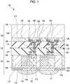
- Fig. 1is a sectional view of a solid-state image pickup apparatus 100 corresponding to the solid-state image pickup apparatus 300 shown in Fig. 12 .
- Fig. 1is a sectional view that is in correspondence with the photoelectric conversion elements 303, the transfer transistors 304, and the amplification transistors 306 shown in Fig. 12 . The other portions are not described.
- Fig. 1shows a structure for two pixels.
- Fig. 1shows a first chip 101, a second chip 102, and a bonding surface 103 of the first chip and the second chip.
- the first chip 101corresponds to the first chip 308 shown in Fig. 12
- the second chip 102corresponds to the second chip 309 shown in Fig. 12 .
- the first chip 101has a first substrate 104.
- a surface of the first substrate 104 where a transistor is formedis a principal surface 105, and a surface thereof opposite thereto is a back surface 106.
- a portion constituting the photoelectric conversion element 303 and the transfer transistor 304 shown in Fig. 12is disposed at the first substrate 104.
- a multilayer wiring structure 107including a first wiring layer 122 and a second wiring layer 123, which, for example, have wires whose main component is aluminum (aluminum wires), is provided on an upper portion at a principal-surface-105-side of the first substrate 104 of the first chip 101.
- a plurality of interlayer insulating films of the multilayer wiring structure 107are described as an integral insulating film.
- the second chip 102has a second substrate 108.
- a surface of the second substrate 108 where a transistor is formedis a principal surface 109, and a surface thereof opposite thereto is a back surface 110.
- a multilayer wiring structure 111including a first wiring layer 128 and a second wiring layer 129, which, for example, have aluminum wires, is provided on an upper portion of the principal surface 109 of the second substrate 108. Even here, a plurality of interlayer insulating films of the multilayer wiring structure 111 are described as an integral insulating film.
- an amplification transistor 306 shown in Fig. 12is disposed at the second substrate 108.
- a direction from the principal surface of the substrate to the back surfaceis defined as a downward direction or a deep direction
- a direction from the back surface to the principal surfaceis defined as an upward direction or a shallow direction.
- the substrate principal surface 105 of the first chip 101 and the substrate principal surface 109 of the second chip 102are placed upon each other so as to face each other.
- a connection between a floating diffusion region (FD region) 113 of the first chip 101 and the gate electrode 126 of an amplification transistor 126 of the second chip 102is only shown.
- the FD region 113 of the first chip 101is connected to the gate electrode 126 of the amplification transistor through the multilayer wiring structure 107, a connection portion 311, and the multilayer wiring structure 111.
- the connection portion 310 shown in Fig. 12 that supplies a control signal to the gate electrode 114 of the transfer transistoris not shown in Fig. 1 .
- the solid-state image pickup apparatus according to the embodimentis a backside-illumination solid-state image pickup apparatus upon which light is incident from the back surface 106 of the first substrate 104.
- a well 115, an N-type charge storage region 112 constituting the photoelectric conversion element, and the gate electrode 114 of the transfer transistorare disposed at the first substrate 104 of the first chip 101. Further, a P-type surface protection layer constituting the photoelectric conversion element is disposed on the upper portion of the charge storage region 112. Further, a P-type semiconductor region 116, an element isolation region 117, and the drain region 113 of the transfer transistor are disposed at the first substrate 104.
- the well 115is a semiconductor region where the transistor and the photoelectric conversion element are disposed, and, here, may be either a N type or a P type.
- the P-type semiconductor region 116can suppress dark current generated at an interface between a silicon oxide film and silicon of the back surface 106 of the first substrate 104, and can even function as a portion of the photoelectric conversion element.
- the charge storage region 112stores electric charge (electrons) generated at the photoelectric conversion element, and has a P-type surface protective layer at a gate-electrode-side of the transfer transistor in Fig. 1 .
- the element isolation region 117is formed of a P-type semiconductor region, and, although not shown, may have an element isolation structure including an insulating film such as a LOCOS isolation layer or a STI isolation layer.
- the drain region 113 of the transfer transistoris an FD region, and constitutes the node 305 shown in Fig. 12 .
- a back-surface-106-side of the first substrate 104 of the first chip 101is provided with an antireflection film 118, a light-shielding film 119, a color filter layer 120 including a planarizing layer, and a microlens 121.
- a well 124, a source region and drain region 125, and the gate electrode 126 of the amplification transistor 306 in Fig. 12 , and an element isolation region 127are disposed at the second substrate 108 of the second chip 102.
- the well 124is a P-type semiconductor region.
- the source region and drain region 125 of the transistor (the amplification transistor 306 shown in Fig. 12 ), disposed at the second chip 102 of the solid-state image pickup apparatus,include a high-melting-point-metal compound layer 130.
- the transistor 12disposed at the second chip 102, is also similarly provided with a transistor including a high-melting-point-metal compound layer (not shown).
- the high-melting-point-metal compound layeris, for example, silicide using cobalt or titanium, which is a high-melting-point metal, when silicon is used in the semiconductor substrate.
- a high-melting-point-metal compound layeris not formed at, for example, the transistor of the first substrate 104.
- the insulating film of a multilayer wiring structureis disposed at the upper portion of the principal surface 105 of the first substrate 104. Accordingly, a high-melting-point-metal compound layer is not formed at the first substrate 104 and the transistor of the peripheral circuit portion disposed at the second substrate has a high-melting-point-metal compound layer, so that it is possible to increase the speed of operation of the transistor while reducing noise.
- the transistor including such a high-melting-point-metal compound layeronly at the second chip 102, it is possible to reduce mixing of the high-melting-point metal into the photoelectric conversion element, and to reduce noise generated by the mixture of the high-melting-point metal. Since it is not necessary to form a region where a high-melting-point-metal compound layer is to be provided and a region where a high-melting-point-metal compound layer is not to be provided on the same substrate, it is not necessary to form, for example, a protective film to prevent the formation of a high-melting-point-metal compound layer, that is, it is possible for each substrate to have a simple structure and to manufacture it using a simple step.
- the FD regionis formed at the first substrate 104. This is because, if a high-melting-point-metal compound layer is provided at the photoelectric conversion element and the semiconductor region constituting the FD region which hold signal charges generated at the photoelectric conversion element, noise generated when a high-melting-point metal is mixed into the semiconductor region mixes in the signal electric charges.
- the amplification transistoris disposed at the first substrate and a high-melting-point-metal compound layer is not formed at the amplification transistor.
- each wiring layeris formed of aluminum wires
- each wiring layermay be formed of wires whose main component is copper (copper wires).
- a diffusion prevention film, which prevents diffusion of copper,may also be provided at upper portions of the copper wires, and the diffusion prevention film, which prevents diffusion of copper, may be subjected to patterning.
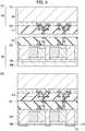
- a solid-state image pickup apparatuswill be described with reference to Fig. 2 .
- the solid-state image pickup apparatus according to the embodimentis similar to the solid-state image pickup apparatus according to the first embodiment in that its circuits are equivalent to those shown in Fig. 12 , and differs therefrom in its chip stacking structure. A description of the circuits will hereunder be omitted. The structure shown in Fig. 2 will hereunder be described.
- Fig. 2is a sectional view of a solid-state image pickup apparatus 200 corresponding to the circuits shown in Fig. 12 .
- Fig. 2is a sectional view for two pixels in correspondence with the photoelectric conversion elements 303, the transfer transistors 304, and the amplification transistors 306 shown in Fig. 12 , and does not show the other portions.
- Fig. 2shows a first chip 201, a second chip 202, and a bonding surface 203 of the first chip and the second chip.
- the first chip 201corresponds to the first chip 308 shown in Fig. 12
- the second chip 202corresponds to the second chip 309 shown in Fig. 12 .
- the first chip 201has a first substrate 204.
- a surface of the first substrate 204 where a transistor is formedis a principal surface 205, and a surface thereof opposite thereto is a back surface 206.
- a portion constituting the photoelectric conversion element 303 and the transfer transistor 304 shown in Fig. 12is disposed at the first substrate 204.
- a multilayer wiring structure 207including a first wiring layer 222 and a second wiring layer 223, which, for example, have aluminum wires, is provided on an upper portion at the principal surface 205 of the first substrate 204.
- a plurality of interlayer insulating films of the multilayer wiring structure 207are described as an integral insulating film.
- the second chip 202has a second substrate 208.
- a surface of the second substrate 208 where a transistor is formedis a principal surface 209, and a surface thereof opposite thereto is a back surface 210.
- a multilayer wiring structure 211including a first wiring layer 228 and a second wiring layer 229, which, for example, have aluminum wires, is provided on an upper portion of the principal surface 209 of the second substrate 208. Even here, a plurality of interlayer insulating films of the multilayer wiring structure 211 are described as an integral insulating film.
- An amplification transistor 306 shown in Fig. 12is disposed at the second substrate 208.
- the principal surface 205 of the first substrate 204 and the back surface 210 of the second substrate 208are placed upon each other so as to face each other.
- a connection between an FD region 213 of the first chip 201 and a gate electrode 226 of an amplification transistor of the second chip 202is only shown. More specifically, the FD region 213 of the first chip 201 is connected to the gate electrode 226 of the amplification transistor through the multilayer wiring structure 207, a connection portion 311, and the multilayer wiring structure 211.
- a through electrode 235constituting a portion of the connection portion 311 and related to the second substrate 208 is disposed.
- the through electrodeBy the through electrode, the FD region 213 and the gate electrode 226 of the amplification transistor are connected to each other.
- the connection portion 310 shown in Fig. 12 that supplies a control signal to the gate electrode 214 of the transfer transistoris not shown in Fig. 2 .
- the solid-state image pickup apparatus according to the embodimentis a backside-illumination solid-state image pickup apparatus upon which light is incident from the back surface 206 of the first substrate 204.
- a well 215, an N-type charge storage region 212, constituting the photoelectric conversion element, and the gate electrode 214 of the transfer transistorare disposed at the first substrate 204 of the first chip 201. Further, a P-type semiconductor region 216, an element isolation region 217, and the drain region 213 of the transfer transistor are disposed at the first substrate 204.
- a back-surface-206-side of the first substrate 204 of the first chip 201is provided with an antireflection film 218, a light-shielding film 219, a color filter layer 220 including a planarizing layer, and a microlens 121.
- a well 224, a source region and drain region 225, and the gate electrode 226 of the amplification transistor 306 in Fig. 12 , and an element isolation region 227are disposed at the second substrate 208 of the second chip 202.
- the first wiring layer 228 and the second wiring layer 229are provided at the upper portion of the second substrate 208, and an insulating layer 234 is provided at a deepest portion of the second substrate 208.
- the structures of the first chip 201 and the second chip 202are similar to those of the first embodiment, so that they will not be described below.
- an adhesive layer 232 and a supporting base 233are further provided at the upper portion of the second chip 202.
- the insulating layer, the adhesive layer 232, and the supporting base 233 in the second embodimentwill be described later.
- the source region and drain region 225 and the gate electrode 226 of the transistor (the amplification transistor 306 shown in Fig. 12 ) disposed at the second chip 202 of the solid-state image pickup apparatushave high-melting-point-metal compound layers 230.
- the high-melting-point-metal compound layeris, for example, silicide using cobalt or titanium, which is a high-melting-point metal, when silicon is used in the semiconductor substrate.
- the transistor of, for example, the peripheral circuit portion disposed at the second substratehas a high-melting-point-metal compound layer, so that it is possible to increase the speed of operation of the transistor.
- the transistor including such a high-melting-point-metal compound layer only at the second chip 202it is possible to reduce mixing of the high-melting-point metal into the photoelectric conversion element, while suppressing a reduction in the characteristics of the photoelectric conversion element of the first chip 201.
- a solid-state image pickup apparatuswill be described with reference to Fig. 3 .
- the solid-state image pickup apparatus according to the embodimentcorresponds to the solid-state image pickup apparatus 100 according to the first embodiment, and differs therefrom in that it includes a diffusion prevention film.
- the structure shown in Fig. 3will hereunder be described. The structural features that are equivalent to those of the first embodiment will not be described.
- a diffusion prevention film 131is disposed between a first chip 101 and a second chip 102.
- a diffusion prevention film 131it is possible to suppress diffusion of a high-melting-point metal of a high-melting-point-metal compound layer disposed at the second chip into multilayer wiring structures 111 and 107 and mixture of the high-melting-point metal into a semiconductor region constituting an FD region and a photoelectric conversion element of the first chip. Therefore, it is possible to further suppress generation of leakage current causing a white defect (of an image) or a dark current to be produced when the high-melting-point metal is mixed into the semiconductor region.
- a photo-diode formation member (hereunder referred to as "PD formation member”) 401which becomes a first substrate 104 shown in Fig. 3
- a circuit formation member 402which becomes a second substrate 108 shown in Fig. 3
- These membersare, for example, silicon semiconductor substrates, and may be of any conductivity type.
- the PD formation member 401includes a p-type semiconductor region 116 and an insulating layer 403.
- the PD formation member 401uses an SOI substrate, and the p-type semiconductor region 116 may be formed by epitaxial growth or ion implantation.
- the multilayer wiring structure 107is formed on the upper portion of the PD formation member 401.
- the multilayer wiring structure 107has a first wiring layer 122 and a second wiring layer 123.
- the first wiring layer 122 and the second wiring layer 123include a plurality of wires.
- the wires in the embodimentare aluminum wires.
- the multilayer wiring structure 107has an interlayer insulating film for insulating the wires from each other.
- the interlayer insulating filmis disposed between the first wiring layer 122 and the gate electrode of the transfer transistor, and between the first wiring layer 122 and the second wiring layer 123.
- a general semiconductor processmay be used for forming the multilayer wiring structure 107.
- an interlayer insulating film covering the second wiring layeris formed, and portions thereof are removed so that some wires of the second wiring layer 123 are exposed.
- the exposed second wiring layer 123constitute a connection portion 311.
- a surface of the PD formation member 401 where the gate electrode of the transfer transistor is formedbecomes a principal surface 105 of the first substrate described later.
- a well 124 and a peripheral circuit portion including a transistor such as an amplification transistor 306are formed at the circuit formation member 402.
- a high-melting-point metalis deposited on predetermined positions, such as a source region, a drain region 125, and a gate electrode 126 of the transistor, and heat treatment is performed, thereby forming a high-melting-point-metal compound layer 130.
- a multilayer wiring structure 111is formed at the upper portion of the circuit formation member 402.
- the multilayer wiring structure 111has a first wiring layer 128 and a second wiring layer 129.
- the structure and production method of the multilayer wiring structure 111are similar to those of the multilayer wiring structure 107 of the PD formation member 401.
- a diffusion prevention film 131 covering the second wiring layer 129is formed.
- the diffusion prevention film 131is formed of, for example, silicon nitride or silicon carbide.
- the diffusion prevention film 131is for suppressing diffusion to the high-melting-point metal PD formation member 401.
- portions of the diffusion prevention film 131are removed so that some wires of the second wiring layer 129 constituting the connection portion 311 are exposed.
- the diffusion prevention filmmay be removed by etching or CMP technology.
- the circuit formation member 402becomes the second substrate 108.
- a principal surface 109 of the second substrate 108is determined as shown in Fig. 4(b) .
- the principal surfaces (105, 109) of the PD formation member 401 and the circuit formation member 402are disposed so as to face each other, and are joined to each other by, for example, a micro-bump.
- an undesired portion 404 and the insulating layer 403 of the PD formation member 401are removed by, for example, CMP or etching, so that the PD formation member 401 is made thinner, to form the first substrate 104.
- an antireflection film 118formed of silicon carbide, is formed at the upper portion of a back surface 106 of the first substrate 104.
- a tungsten filmis formed at the upper portion of the antireflection film 118 for patterning, thereby forming a light-shielding film 119.
- a planarizing layer and a color filter 120are formed, and a microlens 121 is formed.
- Such a production methodmakes it possible to produce the solid-state image pickup apparatus 400 shown in Fig. 3 .
- the interlayer insulating film of the multilayer wiring structure 107after forming the interlayer insulating film of the multilayer wiring structure 107, it is possible to perform heat treatment at a high-temperature or for a long time for improving characteristics such as recovery from defects of the photoelectric conversion element.
- a high-melting-point metal semiconductor compound layeris formed before forming the interlayer insulating film.
- the solid-state image pickup apparatus of the embodimentit is possible to further suppress generation of dark current at the photoelectric conversion element while increasing the speed of operation of the transistor at the peripheral circuit portion and increasing the speed of a signal readout operation.
- a solid-state image pickup apparatuswill be described with reference to Fig. 6 .
- the structure of the solid-state image pickup apparatus according to this embodimentcorresponds to the structure of the solid-state image pickup apparatus according to the second embodiment, and differs therefrom in that it includes a diffusion prevention film.
- the structure shown in Fig. 6will hereunder be described. The structural features that are equivalent to those of the second embodiment will not be described.
- a diffusion prevention film 231which prevents diffusion of a high-melting-point metal, is disposed between a first chip 201 and a second chip 202.
- a diffusion prevention film 231it is possible to further suppress mixing of a high-melting-point metal of a high-melting-point-metal compound layer disposed at the second chip into a semiconductor region constituting an FD region and a photoelectric conversion element of the first chip. Therefore, it is possible to suppress production of a white defect (of an image) or a dark current.
- the diffusion prevention film 231is a film formed of, for example, silicon nitride or silicon carbide.
- a photo-diode formation substrate (hereunder referred to as "PD formation member”) 501which becomes a first substrate 204 shown in Fig. 6
- a circuit formation member 502which becomes a second substrate 208 shown in Fig. 6
- the PD formation member 501includes a p-type semiconductor region 216 and an insulating layer 503.
- the PD formation member 501uses an SOI substrate, and the p-type semiconductor region 216 may be formed by epitaxial growth or ion implantation.
- the circuit formation member 502uses an SOI substrate and includes an insulating layer 234.
- a multilayer wiring structure 207is formed on the upper portion of the PD formation member 501.
- the multilayer wiring structure 207includes a first wiring layer 222 and a second wiring layer 223.
- the structure and production method of the multilayer wiring structure 207are similar to those of the third embodiment, so that they will not be described.
- an interlayer insulating film covering the second wiring layer 223is formed, and portions of the interlayer insulating film are removed so that wires of the second wiring layer 223 are exposed.
- the second wiring layer 223constitutes a connection portion 311.
- a diffusion prevention film 231 covering the second wiring layer 223 and formed of, for example, silicon nitride or silicon carbideis formed.
- the interlayer insulating film covering the second wiring layer 233may be disposed between the second wiring layer 223 and the diffusion prevention film 231.
- a transistor including an amplification transistor and a well 224are formed in the circuit formation member 502 shown in Fig. 7(b) .
- a high-melting-point metalis deposited on predetermined positions, such as a source region, a drain region, and a gate electrode of the transistor, and heat treatment is performed, thereby forming a high-melting-point-metal compound layer 230.
- a multilayer wiring structure 211is formed on the upper portion of the circuit formation member 502.
- the multilayer wiring structure 211has a first wiring layer 228.
- the structure and production method of the first wiring layer 228are similar to those of the third embodiment.
- an adhesive layer 506 and a supporting base 507are formed at the upper portion of the first wiring layer 228 at the circuit formation member 502. Then, an undesired portion 504 of the circuit formation member 502 is removed by abrasion or etching, and the second substrate 208 is formed.
- a principal surface 205 of the PD formation member 501, which becomes the first substrate 204 shown in Fig. 6 , and a back surface 210 of the second substrate 208are placed upon each other so as to face each other, and are joined together by, for example, a micro-bump. Then, the first adhesive layer 506 and the first supporting base 507 are removed. Thereafter, an interlayer insulating film is formed on the upper portion of the first wiring layer 228 at the second substrate 208, and a through electrode 235 for electrical connection with the first substrate 204 is formed.
- the through electrode 235may be produced by a general semiconductor process. Then, the through electrode 235 is covered, and the second wiring layer 229 is formed.
- an adhesive layer 232 and a supporting base 233are provided on the upper portion of the second wiring layer 229 at the second substrate 208.
- an undesired portion 505 at the PD formation member 501is removed by, for example, CMP or etching, and the first substrate 204 is formed.
- an antireflection film 218, formed of, for example, silicon nitrideis formed at the upper portion of a back surface 206 of the first substrate 204.
- a light-shielding film 219formed of, for example, tungsten, is formed at the upper portion of the antireflection film 218.
- a planarizing layer and a color filter 120are formed at the upper portion of the light-shielding film 219, and a microlens 121 is formed.
- Such a production methodmakes it possible to produce the solid-state image pickup apparatus 500 shown in Fig. 6 .
- the solid-state image pickup apparatus of the embodimentit is possible to further suppress generation of dark current at the photoelectric conversion element while increasing the speed of operation of the transistor at the peripheral circuit portion and increasing the speed of a signal readout operation.
- a solid-state image pickup apparatuswill be described with reference to Fig. 10 .
- the structures of solid-state image pickup apparatuses 600, 610, and 620 according to the embodiment shown in Fig. 10correspond to the structure of the solid-state image pickup apparatus 400 according to the third embodiment, with the disposition of the diffusion prevention film 131 being modified.
- the structural features that are equivalent to those of the third embodimentwill not be described below.
- the diffusion prevention film 131is disposed between a first substrate 104 and a second substrate 108, and serves as an interlayer insulating film included in a multilayer wiring structure 107 disposed at the upper portion of the first substrate 104.
- the solid-state image pickup apparatus 600is a backside-illumination solid-state image pickup apparatus, even if the diffusion prevention film 131, formed of, for example, silicon nitride, is provided on the entire top surface of a photoelectric conversion element, for example, reflection resulting from the difference between the refractive indices of the diffusion prevention film 131 and a silicon oxide film, which is a general interlayer insulating film, does not occur. Therefore, it is possible to suppress diffusion of a high-melting-point metal from the second substrate 108 while suppressing a reduction in the optical characteristics.
- the structure in which the diffusion prevention film 131 serves as an interlayer insulating filmis not limited to the structure shown in Fig. 10(a) .
- an interlayer insulating film in a multilayer wiring structure 111 disposed at the upper portion of the second substrate 108may be used.
- the diffusion prevention film 131is disposed between a first substrate 104 and a second substrate 108.
- the diffusion prevention film 131is formed so as to contact a high-melting-point-metal compound layer 130 on a source region and drain region 125 and a gate electrode 126 at the second substrate 108.
- the diffusion prevention film 131is disposed between a first substrate 104 and a second substrate 108, and contacts the upper portion of a first wiring layer 228 at the second substrate 108.
- the first wiring layer 228is formed of copper wires.
- the diffusion prevention film 131also functions as a diffusion prevention film, which prevents diffusion of copper. By virtue of such a structure, it is possible to omit the step of forming the diffusion prevention film, which prevents diffusion of copper, and to make the solid-state image pickup apparatus thin.
- the structure in which the diffusion prevention film 131 serves as a diffusion prevention film, which prevents diffusion of copperis not limited to the structure shown in Fig. 10(c) .
- a multilayer wiring structure 107 disposed on the upper portion of the first substrate 104may be formed of copper wires, and the diffusion prevention film 131 may be formed for each wiring layer.
- a solid-state image pickup apparatuswill be described with reference to Fig. 11 .
- the structures of solid-state image pickup apparatuses 700, 710, and 720 according to the embodiment shown in Fig. 11correspond to the structure of the solid-state image pickup apparatus 500 according to the fourth embodiment, with the disposition of the diffusion prevention film 231 being modified.
- the structural features that are equivalent to those of the fourth embodimentwill not be described below.
- the diffusion prevention film 231is disposed between a first substrate 204 and a second substrate 208, and serves as an interlayer insulating film included in a multilayer wiring structure 207 disposed at the upper portion of the first substrate 104.
- the solid-state image pickup apparatus 700is a backside-illumination solid-state image pickup apparatus.
- the diffusion prevention film 231formed of, for example, silicon nitride, is provided on the entire top surface of a photoelectric conversion element, it is not necessary to consider reflection of incident light resulting from the difference between the refractive indices of the diffusion prevention film 231 and a silicon oxide film, which is a general interlayer insulating film. Therefore, it is possible to suppress diffusion of a high-melting-point metal from the second substrate 208.
- the diffusion prevention film 231is disposed between a first substrate 204 and a second substrate 208, and contacts the upper portion of a first wiring layer 222 at the first substrate 208.
- the first wiring layer 222is formed of copper wires.
- the diffusion prevention film 231also functions as a diffusion prevention film, which prevents diffusion of copper. By virtue of such a structure, it is possible to omit the step of forming the diffusion prevention film, which prevents diffusion of copper, and to make the solid-state image pickup apparatus thin.
- the structure in which the diffusion prevention film 231 serves as a diffusion prevention film, which prevents diffusion of copperis not limited to the structure shown in Fig. 11(b) .
- the second wiring layer 223may be formed of copper wires, and the diffusion prevention film 231 may be disposed on the upper portion of the second wiring layer 223.
- the diffusion prevention film 231may be disposed at the upper portion of the first wiring layer 222.
- a multilayer wiring structure 211, disposed on the upper portion of a second substrate 208may be formed of copper wires, and may include a copper diffusion prevention film 901.
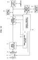
- the image pickup systemmay be, for example, a digital still camera or a digital camcorder.
- reference numeral 1denotes a barrier for protecting a lens
- reference numeral 2denotes a lens where an optical image of an object is formed at an image pickup apparatus 4
- reference numeral 3denotes an aperture stop for varying the quantity of light transmitted through the lens 2.
- Reference numeral 4denotes the image pickup apparatus, which is the solid-state image pickup apparatus described in any of the aforementioned embodiments.
- the image pickup apparatus 4converts the optical image formed by the lens 2 as image data.
- an AD converteris disposed at the image pickup apparatus 4. More specifically, the AD converter is formed at the second chip.
- Reference numeral 7denotes a signal processing section that performs various corrections and data compression on image pickup data output from the image pickup apparatus 4.
- reference numeral 8denotes a timing generating section that outputs various timing signals to the image pickup apparatus 4 and the signal processing section 7
- reference numeral 9denotes an overall control/operation section that performs various operations and that controls the entire digital still camera.
- Reference numeral 10denotes a memory section that temporarily stores the image data
- reference numeral 11denotes an interface section for performing a recording operation or a readout operation on a recording medium
- reference numeral 12denotes the recording medium that is removable, such as a semiconductor memory for recording or reading out the image pickup data.
- reference numeral 13denotes an interface section for performing communication with, for example, an external computer.
- a timing signalmay be input from outside the image pickup system, and the image pickup system may include at least the image pickup apparatus 4 and the signal processing section 7 that processes an image pickup signal output from the image pickup apparatus.
- the image pickup apparatus and the AD convertermay be provided at different chips.
- the signal processing section 7, etc.may be provided at the image pickup apparatus 4. Since a high-melting-point-metal compound layer is formed at the second chip of the image pickup apparatus 4, signal processing, etc. can be performed at a high speed. Accordingly, the photoelectric conversion apparatus according to the present invention is applicable to an image pickup system. By applying the photoelectric conversion apparatus according to the present invention to an image pickup apparatus, high-speed shooting can be performed.
- the solid-state image pickup apparatusmakes it possible to provide a solid-state image pickup apparatus that can perform high-speed operations. Further, the diffusion prevention film makes it possible to reduce dark current, and to suppress the production of a white defect in an image.
- the solid-state image pickup apparatusmay include a plurality of diffusion prevention films, which prevents diffusion of a high-melting-point metal.
- the high-melting-point-metal compound layermay be formed at a portion where an electrical potential is applied to a semiconductor region, such as a well contact, in addition to the source region, the drain region, and the gate electrode of a transistor.
- a semiconductor regionsuch as a well contact
- the present inventionis applicable to a solid-state image pickup apparatus used in an image pickup system, such as a digital still camera or a digital camcorder.
Landscapes
- Engineering & Computer Science (AREA)
- Multimedia (AREA)
- Signal Processing (AREA)
- Solid State Image Pick-Up Elements (AREA)
- Transforming Light Signals Into Electric Signals (AREA)
Description
- The present invention relates to a backside-illumination solid-state image pickup apparatus.
- Recent higher-speed solid-state image pickup apparatuses have caused the proposal of a structure in which a semiconductor compound layer is provided at a transistor.
JP2001111022 JP2009170448 - Prior art which is related to this field of technology can be found in e.g. document
US 2006/0146233 A1 disclosing an image sensor with an enlarged photo detection area and a method for fabricating the same, in documentUS 2006/0141661 A1 disclosing a CMOS image sensor and a method of fabricating the same, in documentUS 2009/0008688 A1 disclosing unit pixels, image sensors and methods of manufacturing the same, in documentWO 2008/156274 A1 disclosing a pixel array preventing the cross talk between unit pixels and an image sensor using the pixel, and in documentEP 1 075 028 A2 disclosing a photoelectric conversion device and a process for its fabrication. - In the structure in which a high-melting-point-metal semiconductor compound layer is provided at the peripheral circuit portion in
JP2001111022 JP2001111022 - Accordingly, it is an object of the present invention to provide, by using a simple structure, a solid-state image pickup apparatus in which a silicide layer is disposed at a peripheral circuit portion while a reduction in the characteristics of a photoelectric conversion element, which causes, for example, a white defect to be produced, is suppressed.
- The present invention provides a solid-state image pickup apparatus and an image pickup system according to the respective claims.
- According to the present invention, it is possible to provided, by using a simple structure, a solid-state image pickup apparatus in which a silicide layer is disposed at a peripheral circuit portion while a reduction in the characteristics of a photoelectric conversion element is suppressed.
Fig. 1 is a sectional view of a solid-state image pickup apparatus used to describe a first example not forming part of the claimed invention.Fig. 2 is a sectional view of a solid-state image pickup apparatus used to describe a second example not forming part of the claimed invention.Fig. 3 is a sectional view of a solid-state image pickup apparatus used to describe a third example not forming part of the claimed invention.Fig. 4 shows a method of manufacturing the solid-state image pickup apparatus according to the third example not forming part of the claimed invention.Fig. 5 shows the method of manufacturing the solid-state image pickup apparatus according to the third example not forming part of the claimed invention.Fig. 6 is a sectional view of a solid-state image pickup apparatus used to describe a fifth example not forming part of the claimed invention.Fig. 7 shows a method of manufacturing a solid-state image pickup apparatus according to a fourth example not forming part of the claimed invention.Fig. 8 shows the method of manufacturing the solid-state image pickup apparatus according to the fourth example not forming part of the claimed invention.Fig. 9 shows the method of manufacturing the solid-state image pickup apparatus according to the fourth example not forming part of the claimed invention.Fig. 10 is a sectional view of the solid-state image pickup apparatus used to describe the fifth example not forming part of the claimed invention.Fig. 11 is a sectional view of a solid-state image pickup apparatus used to describe a sixth example not forming part of the claimed invention.Fig. 12 is an exemplary circuit of the solid-state image pickup apparatus according to the present invention.Fig. 13 is a block diagram illustrating an image pickup system according to a seventh embodiment.- A solid-state image pickup apparatus according to the present invention is formed by placing a first substrate and a second substrate upon each other, with the first substrate being provided with a photoelectric conversion element and a gate electrode for transfer and the second substrate being provided with a peripheral circuit portion. A silicide layer is not provided at the first substrate, whereas a silicide layer is provided at the second substrate. By such a structure, it becomes easier to determine where to form the compound layer, and it becomes possible for a transistor at the peripheral circuit portion to operate at a higher speed, and a signal readout operation to be performed at a high speed while suppressing a reduction in the characteristics of the photoelectric conversion element.
- The present invention will hereunder be described in detail with reference to the drawings. In the following, the expression "high-melting-metal compound" is to be interpreted as "silicide". Furthermore, several embodiments and examples are disclosed in the following: However, it is understood that embodiments of the invention are only those covered by the appended claims, in particular the amplification transistor is disposed at the first substrate according to the invention.
- A first embodiment of the present invention will be described with reference to
Figs. 1 and12 . - First, an exemplary circuit of a solid-state image pickup apparatus according to the first embodiment will be described with reference to
Fig. 12 . A solid-stateimage pickup apparatus 300 shown inFig. 12 includes apixel portion 301, in which a plurality of photoelectric conversion elements are arranged, and aperipheral circuit portion 302, provided with a control circuit for performing a driving operation for reading out a signal from thepixel portion 301 and with a signal processing circuit that processes the readout signal. - In the
pixel portion 301, a plurality ofphotoelectric conversion elements 303,transfer transistors 304,amplification transistors 306, andreset transistors 307 are disposed. A structure including at least onephotoelectric conversion element 303 is defined as a pixel. One pixel in the embodiment includes thephotoelectric conversion element 303, thetransfer transistor 304, theamplification transistor 306, and thereset transistor 307. A source of thetransfer transistor 304 is connected to thephotoelectric conversion element 303, and a drain region of thetransfer transistor 304 is connected to a gate electrode of theamplification transistor 306. A node corresponding to the gate electrode of theamplification transistor 306 is defined as anode 305. The reset transistor is connected to thenode 305, and an electric potential of thenode 305 is set to any electric potential (for example, a reset electric potential). Here, theamplification transistor 306 is a portion of a source follower circuit, and a signal corresponding to the electric potential of thenode 305 is output to a signal line RL. - The
peripheral circuit portion 302 includes a vertical scanning circuit VSR for supplying a control signal to the gate electrode of the transistor of thepixel portion 301. Theperipheral circuit portion 302 includes a readout circuit RC holding a signal output from thepixel portion 301 and including a signal processing circuit for amplification, addition, AD conversion, etc. In addition, theperipheral circuit portion 302 includes a horizontal scanning circuit HSR of a control circuit that controls timing with which signals from the readout circuit RC are successively output. - Here, the solid-state
image pickup apparatus 300 according to the first embodiment is formed by placing two chips upon each other. In an example not forming part of the claimed invention, the two chips are afirst chip 308 including aphotoelectric conversion element 303 and atransfer transistor 304 of thepixel portion 301, and asecond chip 309 including anamplification transistor 306 and areset transistor 307 of thepixel portion 301 and theperipheral circuit portion 302. In such a structure, a control signal is supplied to the gate electrode of thetransfer transistor 304 of thefirst chip 308 from theperipheral circuit portion 302 of thesecond chip 309 through aconnection portion 310. A signal generated at thephotoelectric conversion element 303 of thefirst chip 308 is read out to thenode 305 through aconnection portion 311 connected to the drain region of thetransfer transistor 304. By providing thereset transistor 307 and theamplification transistor 306 at a different chip in this way, it is possible to increase the area of thephotoelectric conversion element 303, and to increase sensitivity. If the area of thephotoelectric conversion element 303 is the same, manyphotoelectric conversion elements 303 can be provided, thereby making it possible to increase the number of pixels. - Next, a solid-state image pickup apparatus according to an example will be described with reference to
Fig. 1. Fig. 1 is a sectional view of a solid-stateimage pickup apparatus 100 corresponding to the solid-stateimage pickup apparatus 300 shown inFig. 12 .Fig. 1 is a sectional view that is in correspondence with thephotoelectric conversion elements 303, thetransfer transistors 304, and theamplification transistors 306 shown inFig. 12 . The other portions are not described.Fig. 1 shows a structure for two pixels. Fig. 1 shows afirst chip 101, asecond chip 102, and abonding surface 103 of the first chip and the second chip. Thefirst chip 101 corresponds to thefirst chip 308 shown inFig. 12 , and thesecond chip 102 corresponds to thesecond chip 309 shown inFig. 12 .- The
first chip 101 has afirst substrate 104. A surface of thefirst substrate 104 where a transistor is formed is aprincipal surface 105, and a surface thereof opposite thereto is aback surface 106. A portion constituting thephotoelectric conversion element 303 and thetransfer transistor 304 shown inFig. 12 is disposed at thefirst substrate 104. Amultilayer wiring structure 107, including afirst wiring layer 122 and asecond wiring layer 123, which, for example, have wires whose main component is aluminum (aluminum wires), is provided on an upper portion at a principal-surface-105-side of thefirst substrate 104 of thefirst chip 101. Here, a plurality of interlayer insulating films of themultilayer wiring structure 107 are described as an integral insulating film. - The
second chip 102 has asecond substrate 108. A surface of thesecond substrate 108 where a transistor is formed is aprincipal surface 109, and a surface thereof opposite thereto is aback surface 110. Amultilayer wiring structure 111, including afirst wiring layer 128 and asecond wiring layer 129, which, for example, have aluminum wires, is provided on an upper portion of theprincipal surface 109 of thesecond substrate 108. Even here, a plurality of interlayer insulating films of themultilayer wiring structure 111 are described as an integral insulating film. In an example not forming part of the claimed invention, anamplification transistor 306 shown inFig. 12 is disposed at thesecond substrate 108. In the description, in each chip, a direction from the principal surface of the substrate to the back surface is defined as a downward direction or a deep direction, and a direction from the back surface to the principal surface is defined as an upward direction or a shallow direction. - Here, in the solid-state image pickup apparatus according to the embodiment, the substrate
principal surface 105 of thefirst chip 101 and the substrateprincipal surface 109 of thesecond chip 102 are placed upon each other so as to face each other. InFig. 1 , in a structure of a connection portion of thefirst chip 101 and thesecond chip 102, a connection between a floating diffusion region (FD region) 113 of thefirst chip 101 and thegate electrode 126 of anamplification transistor 126 of thesecond chip 102 is only shown. In an example being useful to understand the present invention, theFD region 113 of thefirst chip 101 is connected to thegate electrode 126 of the amplification transistor through themultilayer wiring structure 107, aconnection portion 311, and themultilayer wiring structure 111. Theconnection portion 310 shown inFig. 12 that supplies a control signal to thegate electrode 114 of the transfer transistor is not shown inFig. 1 . The solid-state image pickup apparatus according to the embodiment is a backside-illumination solid-state image pickup apparatus upon which light is incident from theback surface 106 of thefirst substrate 104. - Each chip will be described in detail. First, a well 115, an N-type
charge storage region 112 constituting the photoelectric conversion element, and thegate electrode 114 of the transfer transistor are disposed at thefirst substrate 104 of thefirst chip 101. Further, a P-type surface protection layer constituting the photoelectric conversion element is disposed on the upper portion of thecharge storage region 112. Further, a P-type semiconductor region 116, anelement isolation region 117, and thedrain region 113 of the transfer transistor are disposed at thefirst substrate 104. The well 115 is a semiconductor region where the transistor and the photoelectric conversion element are disposed, and, here, may be either a N type or a P type. The P-type semiconductor region 116 can suppress dark current generated at an interface between a silicon oxide film and silicon of theback surface 106 of thefirst substrate 104, and can even function as a portion of the photoelectric conversion element. Thecharge storage region 112 stores electric charge (electrons) generated at the photoelectric conversion element, and has a P-type surface protective layer at a gate-electrode-side of the transfer transistor inFig. 1 . Theelement isolation region 117 is formed of a P-type semiconductor region, and, although not shown, may have an element isolation structure including an insulating film such as a LOCOS isolation layer or a STI isolation layer. Thedrain region 113 of the transfer transistor is an FD region, and constitutes thenode 305 shown inFig. 12 . A back-surface-106-side of thefirst substrate 104 of thefirst chip 101 is provided with anantireflection film 118, a light-shieldingfilm 119, acolor filter layer 120 including a planarizing layer, and amicrolens 121. - In an example not forming part of the claimed invention, a well 124, a source region and drain
region 125, and thegate electrode 126 of theamplification transistor 306 inFig. 12 , and anelement isolation region 127 are disposed at thesecond substrate 108 of thesecond chip 102. The well 124 is a P-type semiconductor region. Here, the source region and drainregion 125 of the transistor (theamplification transistor 306 shown inFig. 12 ), disposed at thesecond chip 102 of the solid-state image pickup apparatus, include a high-melting-point-metal compound layer 130. A region constituting theperipheral circuit portion 302 shown inFig. 12 , disposed at thesecond chip 102, is also similarly provided with a transistor including a high-melting-point-metal compound layer (not shown). The high-melting-point-metal compound layer is, for example, silicide using cobalt or titanium, which is a high-melting-point metal, when silicon is used in the semiconductor substrate. - A high-melting-point-metal compound layer is not formed at, for example, the transistor of the
first substrate 104. The insulating film of a multilayer wiring structure is disposed at the upper portion of theprincipal surface 105 of thefirst substrate 104. Accordingly, a high-melting-point-metal compound layer is not formed at thefirst substrate 104 and the transistor of the peripheral circuit portion disposed at the second substrate has a high-melting-point-metal compound layer, so that it is possible to increase the speed of operation of the transistor while reducing noise. In addition, by providing the transistor including such a high-melting-point-metal compound layer only at thesecond chip 102, it is possible to reduce mixing of the high-melting-point metal into the photoelectric conversion element, and to reduce noise generated by the mixture of the high-melting-point metal. Since it is not necessary to form a region where a high-melting-point-metal compound layer is to be provided and a region where a high-melting-point-metal compound layer is not to be provided on the same substrate, it is not necessary to form, for example, a protective film to prevent the formation of a high-melting-point-metal compound layer, that is, it is possible for each substrate to have a simple structure and to manufacture it using a simple step. - In the embodiment, in addition to the photoelectric conversion element, the FD region is formed at the
first substrate 104. This is because, if a high-melting-point-metal compound layer is provided at the photoelectric conversion element and the semiconductor region constituting the FD region which hold signal charges generated at the photoelectric conversion element, noise generated when a high-melting-point metal is mixed into the semiconductor region mixes in the signal electric charges. The amplification transistor is disposed at the first substrate and a high-melting-point-metal compound layer is not formed at the amplification transistor. - Although, in the embodiment, each wiring layer is formed of aluminum wires, each wiring layer may be formed of wires whose main component is copper (copper wires). A diffusion prevention film, which prevents diffusion of copper, may also be provided at upper portions of the copper wires, and the diffusion prevention film, which prevents diffusion of copper, may be subjected to patterning.
- A solid-state image pickup apparatus according to this embodiment will be described with reference to
Fig. 2 . The solid-state image pickup apparatus according to the embodiment is similar to the solid-state image pickup apparatus according to the first embodiment in that its circuits are equivalent to those shown inFig. 12 , and differs therefrom in its chip stacking structure. A description of the circuits will hereunder be omitted. The structure shown inFig. 2 will hereunder be described. Fig. 2 is a sectional view of a solid-stateimage pickup apparatus 200 corresponding to the circuits shown inFig. 12 .Fig. 2 is a sectional view for two pixels in correspondence with thephotoelectric conversion elements 303, thetransfer transistors 304, and theamplification transistors 306 shown inFig. 12 , and does not show the other portions.Fig. 2 shows afirst chip 201, asecond chip 202, and abonding surface 203 of the first chip and the second chip. Thefirst chip 201 corresponds to thefirst chip 308 shown inFig. 12 , and thesecond chip 202 corresponds to thesecond chip 309 shown inFig. 12 .- The
first chip 201 has afirst substrate 204. A surface of thefirst substrate 204 where a transistor is formed is aprincipal surface 205, and a surface thereof opposite thereto is aback surface 206. A portion constituting thephotoelectric conversion element 303 and thetransfer transistor 304 shown inFig. 12 is disposed at thefirst substrate 204. Amultilayer wiring structure 207, including afirst wiring layer 222 and asecond wiring layer 223, which, for example, have aluminum wires, is provided on an upper portion at theprincipal surface 205 of thefirst substrate 204. Here, a plurality of interlayer insulating films of themultilayer wiring structure 207 are described as an integral insulating film. - The
second chip 202 has asecond substrate 208. A surface of thesecond substrate 208 where a transistor is formed is aprincipal surface 209, and a surface thereof opposite thereto is aback surface 210. Amultilayer wiring structure 211, including afirst wiring layer 228 and asecond wiring layer 229, which, for example, have aluminum wires, is provided on an upper portion of theprincipal surface 209 of thesecond substrate 208. Even here, a plurality of interlayer insulating films of themultilayer wiring structure 211 are described as an integral insulating film. Anamplification transistor 306 shown inFig. 12 is disposed at thesecond substrate 208. - Here, in the solid-state image pickup apparatus, the
principal surface 205 of thefirst substrate 204 and theback surface 210 of thesecond substrate 208 are placed upon each other so as to face each other. InFig. 2 , in a structure of a connection portion of thefirst chip 201 and thesecond chip 202, a connection between anFD region 213 of thefirst chip 201 and agate electrode 226 of an amplification transistor of thesecond chip 202 is only shown. More specifically, theFD region 213 of thefirst chip 201 is connected to thegate electrode 226 of the amplification transistor through themultilayer wiring structure 207, aconnection portion 311, and themultilayer wiring structure 211. Here, a throughelectrode 235 constituting a portion of theconnection portion 311 and related to thesecond substrate 208 is disposed. By the through electrode, theFD region 213 and thegate electrode 226 of the amplification transistor are connected to each other. Theconnection portion 310 shown inFig. 12 that supplies a control signal to thegate electrode 214 of the transfer transistor is not shown inFig. 2 . The solid-state image pickup apparatus according to the embodiment is a backside-illumination solid-state image pickup apparatus upon which light is incident from theback surface 206 of thefirst substrate 204. - Next, each chip will be described in detail. A well 215, an N-type
charge storage region 212, constituting the photoelectric conversion element, and thegate electrode 214 of the transfer transistor are disposed at thefirst substrate 204 of thefirst chip 201. Further, a P-type semiconductor region 216, anelement isolation region 217, and thedrain region 213 of the transfer transistor are disposed at thefirst substrate 204. A back-surface-206-side of thefirst substrate 204 of thefirst chip 201 is provided with anantireflection film 218, a light-shieldingfilm 219, acolor filter layer 220 including a planarizing layer, and amicrolens 121. Next, in an example not forming part of the claimed invention, a well 224, a source region and drainregion 225, and thegate electrode 226 of theamplification transistor 306 inFig. 12 , and anelement isolation region 227 are disposed at thesecond substrate 208 of thesecond chip 202. In addition, thefirst wiring layer 228 and thesecond wiring layer 229 are provided at the upper portion of thesecond substrate 208, and an insulatinglayer 234 is provided at a deepest portion of thesecond substrate 208. The structures of thefirst chip 201 and thesecond chip 202 are similar to those of the first embodiment, so that they will not be described below. - In the second embodiment, an
adhesive layer 232 and a supportingbase 233 are further provided at the upper portion of thesecond chip 202. The insulating layer, theadhesive layer 232, and the supportingbase 233 in the second embodiment will be described later. - Here, in an example not forming part of the claimed invention, the source region and drain
region 225 and thegate electrode 226 of the transistor (theamplification transistor 306 shown inFig. 12 ) disposed at thesecond chip 202 of the solid-state image pickup apparatus have high-melting-point-metal compound layers 230. A region constituting theperipheral circuit portion 302 shown inFig. 12 , disposed at thesecond chip 202, is also similarly provided with a transistor including a high-melting-point-metal compound layer (not shown). The high-melting-point-metal compound layer is, for example, silicide using cobalt or titanium, which is a high-melting-point metal, when silicon is used in the semiconductor substrate. The transistor of, for example, the peripheral circuit portion disposed at the second substrate has a high-melting-point-metal compound layer, so that it is possible to increase the speed of operation of the transistor. In addition, by providing the transistor including such a high-melting-point-metal compound layer only at thesecond chip 202, it is possible to reduce mixing of the high-melting-point metal into the photoelectric conversion element, while suppressing a reduction in the characteristics of the photoelectric conversion element of thefirst chip 201. Since it is not necessary to form a region where a high-melting-point-metal compound layer is to be provided and a region where a high-melting-point-metal compound layer is not to be provided on the same substrate, it is not necessary to form, for example, a protective film to prevent the formation of a high-melting-point-metal compound layer, that is, it is possible for each substrate to have a simple structure and to manufacture it using a simple step. - A solid-state image pickup apparatus according to this embodiment will be described with reference to
Fig. 3 . The solid-state image pickup apparatus according to the embodiment corresponds to the solid-stateimage pickup apparatus 100 according to the first embodiment, and differs therefrom in that it includes a diffusion prevention film. The structure shown inFig. 3 will hereunder be described. The structural features that are equivalent to those of the first embodiment will not be described. - In a solid-state
image pickup apparatus 400 shown inFig. 3 , adiffusion prevention film 131 is disposed between afirst chip 101 and asecond chip 102. By providing such adiffusion prevention film 131, it is possible to suppress diffusion of a high-melting-point metal of a high-melting-point-metal compound layer disposed at the second chip intomultilayer wiring structures - A method of producing the solid-state
image pickup apparatus 400 shown inFig. 3 will be described with reference toFigs. 4 and5 . First, inFig. 4(a) , a photo-diode formation member (hereunder referred to as "PD formation member") 401, which becomes afirst substrate 104 shown inFig. 3 , and acircuit formation member 402, which becomes asecond substrate 108 shown inFig. 3 , are provided. These members are, for example, silicon semiconductor substrates, and may be of any conductivity type. ThePD formation member 401 includes a p-type semiconductor region 116 and an insulatinglayer 403. ThePD formation member 401 uses an SOI substrate, and the p-type semiconductor region 116 may be formed by epitaxial growth or ion implantation. - Next, as shown in
Fig. 4(b) , elements such as agate electrode 114 of a transfer transistor and acharge storage region 112 are formed at thePD formation member 401. Themultilayer wiring structure 107 is formed on the upper portion of thePD formation member 401. Themultilayer wiring structure 107 has afirst wiring layer 122 and asecond wiring layer 123. Thefirst wiring layer 122 and thesecond wiring layer 123 include a plurality of wires. The wires in the embodiment are aluminum wires. Themultilayer wiring structure 107 has an interlayer insulating film for insulating the wires from each other. For example, the interlayer insulating film is disposed between thefirst wiring layer 122 and the gate electrode of the transfer transistor, and between thefirst wiring layer 122 and thesecond wiring layer 123. For forming themultilayer wiring structure 107, a general semiconductor process may be used. Finally, an interlayer insulating film covering the second wiring layer is formed, and portions thereof are removed so that some wires of thesecond wiring layer 123 are exposed. The exposedsecond wiring layer 123 constitute aconnection portion 311. A surface of thePD formation member 401 where the gate electrode of the transfer transistor is formed becomes aprincipal surface 105 of the first substrate described later. - In
Fig. 4(b) , in an example not forming part of the claimed invention, a well 124 and a peripheral circuit portion including a transistor such as anamplification transistor 306 are formed at thecircuit formation member 402. Then, a high-melting-point metal is deposited on predetermined positions, such as a source region, adrain region 125, and agate electrode 126 of the transistor, and heat treatment is performed, thereby forming a high-melting-point-metal compound layer 130. Thereafter, amultilayer wiring structure 111 is formed at the upper portion of thecircuit formation member 402. Themultilayer wiring structure 111 has afirst wiring layer 128 and asecond wiring layer 129. The structure and production method of themultilayer wiring structure 111 are similar to those of themultilayer wiring structure 107 of thePD formation member 401. Next, after forming thesecond wiring layer 129, adiffusion prevention film 131 covering thesecond wiring layer 129 is formed. Thediffusion prevention film 131 is formed of, for example, silicon nitride or silicon carbide. Thediffusion prevention film 131 is for suppressing diffusion to the high-melting-point metalPD formation member 401. Thereafter, portions of thediffusion prevention film 131 are removed so that some wires of thesecond wiring layer 129 constituting theconnection portion 311 are exposed. Here, the diffusion prevention film may be removed by etching or CMP technology. Here, thecircuit formation member 402 becomes thesecond substrate 108. Aprincipal surface 109 of thesecond substrate 108 is determined as shown inFig. 4(b) . - Next, as shown in
Fig. 5(c) , the principal surfaces (105, 109) of thePD formation member 401 and thecircuit formation member 402 are disposed so as to face each other, and are joined to each other by, for example, a micro-bump. - Finally, as shown in
Fig. 5(d) , anundesired portion 404 and the insulatinglayer 403 of thePD formation member 401 are removed by, for example, CMP or etching, so that thePD formation member 401 is made thinner, to form thefirst substrate 104. Thereafter, anantireflection film 118, formed of silicon carbide, is formed at the upper portion of aback surface 106 of thefirst substrate 104. After forming theantireflection film 118, a tungsten film is formed at the upper portion of theantireflection film 118 for patterning, thereby forming a light-shieldingfilm 119. Thereafter, a planarizing layer and acolor filter 120 are formed, and amicrolens 121 is formed. Such a production method makes it possible to produce the solid-stateimage pickup apparatus 400 shown inFig. 3 . - Here, according to the structure of the embodiment, after forming the interlayer insulating film of the
multilayer wiring structure 107, it is possible to perform heat treatment at a high-temperature or for a long time for improving characteristics such as recovery from defects of the photoelectric conversion element. If the first substrate is provided with a high-melting-point-metal compound layer in an example not forming part of the claimed invention, a high-melting-point metal semiconductor compound layer is formed before forming the interlayer insulating film. After forming the interlayer insulating film, it becomes difficult to perform heat treatment at a high temperature or for a long time due to problems such as diffusion of the high-melting-point metal. Therefore, according to the structure of the embodiment, since heat treatment for recovering from defects of the photoelectric conversion element may be optionally performed, it is possible to suppress a reduction in the characteristics of the photoelectric conversion element. - In a desirable form, for increasing connection resistance of a contact provided at an FD region, it is desirable to perform ion implantation and heat treatment on the semiconductor region that is connected to a plug. However, as mentioned above, if the first substrate is provided with a high-melting-point-metal compound layer in an example not forming part of the claimed invention, it becomes difficult to perform heat treatment in a contact formation step that is carried out after forming the interlayer insulating film. Therefore, according to the structure of the embodiment, it is possible to perform sufficient heat treatment in the step of forming the contact at the FD region where the high-melting-point-metal compound layer is not provided while the high-melting-point-metal compound layer is provided at the peripheral circuit portion. Therefore, it is possible to properly connect the contact at the FD region while reducing contamination of the high-melting-point metal at the FD region.
- As discussed above, according to the solid-state image pickup apparatus of the embodiment, it is possible to further suppress generation of dark current at the photoelectric conversion element while increasing the speed of operation of the transistor at the peripheral circuit portion and increasing the speed of a signal readout operation.
- A solid-state image pickup apparatus according to this embodiment will be described with reference to
Fig. 6 . The structure of the solid-state image pickup apparatus according to this embodiment corresponds to the structure of the solid-state image pickup apparatus according to the second embodiment, and differs therefrom in that it includes a diffusion prevention film. The structure shown inFig. 6 will hereunder be described. The structural features that are equivalent to those of the second embodiment will not be described. - In a solid-state
image pickup apparatus 500 shown inFig. 6 , adiffusion prevention film 231, which prevents diffusion of a high-melting-point metal, is disposed between afirst chip 201 and asecond chip 202. By providing such adiffusion prevention film 231, it is possible to further suppress mixing of a high-melting-point metal of a high-melting-point-metal compound layer disposed at the second chip into a semiconductor region constituting an FD region and a photoelectric conversion element of the first chip. Therefore, it is possible to suppress production of a white defect (of an image) or a dark current. Thediffusion prevention film 231 is a film formed of, for example, silicon nitride or silicon carbide. - Next, a method of producing the solid-state
image pickup apparatus 500 shown inFig. 6 will be described with reference toFigs. 7 to 9 . First, inFig. 7(a) , a photo-diode formation substrate (hereunder referred to as "PD formation member") 501, which becomes afirst substrate 204 shown inFig. 6 , and acircuit formation member 502, which becomes asecond substrate 208 shown inFig. 6 , are provided. ThePD formation member 501 includes a p-type semiconductor region 216 and an insulatinglayer 503. ThePD formation member 501 uses an SOI substrate, and the p-type semiconductor region 216 may be formed by epitaxial growth or ion implantation. Thecircuit formation member 502 uses an SOI substrate and includes an insulatinglayer 234. - Next, in the
PD formation member 501 shown inFig. 7(b) , elements such as agate electrode 214 of a transfer transistor, acharge storage region 212, and a well 215 are formed. Amultilayer wiring structure 207 is formed on the upper portion of thePD formation member 501. Themultilayer wiring structure 207 includes afirst wiring layer 222 and asecond wiring layer 223. The structure and production method of themultilayer wiring structure 207 are similar to those of the third embodiment, so that they will not be described. Next, an interlayer insulating film covering thesecond wiring layer 223 is formed, and portions of the interlayer insulating film are removed so that wires of thesecond wiring layer 223 are exposed. Thesecond wiring layer 223 constitutes aconnection portion 311. Then, adiffusion prevention film 231 covering thesecond wiring layer 223 and formed of, for example, silicon nitride or silicon carbide is formed. The interlayer insulating film covering thesecond wiring layer 233 may be disposed between thesecond wiring layer 223 and thediffusion prevention film 231. - In an example not forming part of the claimed invention, in the
circuit formation member 502 shown inFig. 7(b) , a transistor including an amplification transistor and a well 224 are formed. Then, a high-melting-point metal is deposited on predetermined positions, such as a source region, a drain region, and a gate electrode of the transistor, and heat treatment is performed, thereby forming a high-melting-point-metal compound layer 230. Thereafter, amultilayer wiring structure 211 is formed on the upper portion of thecircuit formation member 502. Themultilayer wiring structure 211 has afirst wiring layer 228. The structure and production method of thefirst wiring layer 228 are similar to those of the third embodiment. - Next, in
Fig. 8(c) , anadhesive layer 506 and a supportingbase 507 are formed at the upper portion of thefirst wiring layer 228 at thecircuit formation member 502. Then, anundesired portion 504 of thecircuit formation member 502 is removed by abrasion or etching, and thesecond substrate 208 is formed. - In
Fig. 8(d) , aprincipal surface 205 of thePD formation member 501, which becomes thefirst substrate 204 shown inFig. 6 , and aback surface 210 of thesecond substrate 208 are placed upon each other so as to face each other, and are joined together by, for example, a micro-bump. Then, the firstadhesive layer 506 and the first supportingbase 507 are removed. Thereafter, an interlayer insulating film is formed on the upper portion of thefirst wiring layer 228 at thesecond substrate 208, and a throughelectrode 235 for electrical connection with thefirst substrate 204 is formed. The throughelectrode 235 may be produced by a general semiconductor process. Then, the throughelectrode 235 is covered, and thesecond wiring layer 229 is formed. - Next, as shown in
Fig. 9 , anadhesive layer 232 and a supportingbase 233 are provided on the upper portion of thesecond wiring layer 229 at thesecond substrate 208. Then, anundesired portion 505 at thePD formation member 501 is removed by, for example, CMP or etching, and thefirst substrate 204 is formed. Thereafter, anantireflection film 218, formed of, for example, silicon nitride, is formed at the upper portion of aback surface 206 of thefirst substrate 204. Then, a light-shieldingfilm 219, formed of, for example, tungsten, is formed at the upper portion of theantireflection film 218. Further, a planarizing layer and acolor filter 120 are formed at the upper portion of the light-shieldingfilm 219, and amicrolens 121 is formed. Such a production method makes it possible to produce the solid-stateimage pickup apparatus 500 shown inFig. 6 . - Even in the structure according to the embodiment, since heat treatment of a contact or a photoelectric conversion element can be optionally performed, it is possible to suppress a reduction in the characteristics of the photoelectric conversion element and an increase in the connection resistance of the contact.
- As discussed above, according to the solid-state image pickup apparatus of the embodiment, it is possible to further suppress generation of dark current at the photoelectric conversion element while increasing the speed of operation of the transistor at the peripheral circuit portion and increasing the speed of a signal readout operation.
- A solid-state image pickup apparatus according to this embodiment will be described with reference to
Fig. 10 . The structures of solid-stateimage pickup apparatuses Fig. 10 correspond to the structure of the solid-stateimage pickup apparatus 400 according to the third embodiment, with the disposition of thediffusion prevention film 131 being modified. The structural features that are equivalent to those of the third embodiment will not be described below. - In the solid-state
image pickup apparatus 600 shown inFig. 10(a) , thediffusion prevention film 131 is disposed between afirst substrate 104 and asecond substrate 108, and serves as an interlayer insulating film included in amultilayer wiring structure 107 disposed at the upper portion of thefirst substrate 104. By virtue of such a structure, it is possible to omit the step of forming an interlayer insulating film, and to make the solid-state image pickup apparatus thin. In addition, since the solid-stateimage pickup apparatus 600 is a backside-illumination solid-state image pickup apparatus, even if thediffusion prevention film 131, formed of, for example, silicon nitride, is provided on the entire top surface of a photoelectric conversion element, for example, reflection resulting from the difference between the refractive indices of thediffusion prevention film 131 and a silicon oxide film, which is a general interlayer insulating film, does not occur. Therefore, it is possible to suppress diffusion of a high-melting-point metal from thesecond substrate 108 while suppressing a reduction in the optical characteristics. The structure in which thediffusion prevention film 131 serves as an interlayer insulating film is not limited to the structure shown inFig. 10(a) . For example, an interlayer insulating film in amultilayer wiring structure 111 disposed at the upper portion of thesecond substrate 108 may be used. - Next, in the solid-state
image pickup apparatus 610 shown inFig. 10(b) , thediffusion prevention film 131 is disposed between afirst substrate 104 and asecond substrate 108. In addition, thediffusion prevention film 131 is formed so as to contact a high-melting-point-metal compound layer 130 on a source region and drainregion 125 and agate electrode 126 at thesecond substrate 108. By virtue of such a structure, it is possible to use thediffusion prevention film 131 as an etching stop layer when forming a contact hole of thesecond substrate 108. - Next, in the solid-state
image pickup apparatus 620 shown inFig. 10(c) , thediffusion prevention film 131 is disposed between afirst substrate 104 and asecond substrate 108, and contacts the upper portion of afirst wiring layer 228 at thesecond substrate 108. Thefirst wiring layer 228 is formed of copper wires. Thediffusion prevention film 131 also functions as a diffusion prevention film, which prevents diffusion of copper. By virtue of such a structure, it is possible to omit the step of forming the diffusion prevention film, which prevents diffusion of copper, and to make the solid-state image pickup apparatus thin. The structure in which thediffusion prevention film 131 serves as a diffusion prevention film, which prevents diffusion of copper, is not limited to the structure shown inFig. 10(c) . For example, amultilayer wiring structure 107 disposed on the upper portion of thefirst substrate 104 may be formed of copper wires, and thediffusion prevention film 131 may be formed for each wiring layer. - A solid-state image pickup apparatus according to this embodiment will be described with reference to
Fig. 11 . The structures of solid-stateimage pickup apparatuses Fig. 11 correspond to the structure of the solid-stateimage pickup apparatus 500 according to the fourth embodiment, with the disposition of thediffusion prevention film 231 being modified. The structural features that are equivalent to those of the fourth embodiment will not be described below. - In the solid-state
image pickup apparatus 700 shown inFig. 11(a) , thediffusion prevention film 231 is disposed between afirst substrate 204 and asecond substrate 208, and serves as an interlayer insulating film included in amultilayer wiring structure 207 disposed at the upper portion of thefirst substrate 104. By virtue of such a structure, it is possible to omit the step of forming an interlayer insulating film, and to make the solid-state image pickup apparatus thin. In addition, the solid-stateimage pickup apparatus 700 is a backside-illumination solid-state image pickup apparatus. Therefore, even if thediffusion prevention film 231, formed of, for example, silicon nitride, is provided on the entire top surface of a photoelectric conversion element, it is not necessary to consider reflection of incident light resulting from the difference between the refractive indices of thediffusion prevention film 231 and a silicon oxide film, which is a general interlayer insulating film. Therefore, it is possible to suppress diffusion of a high-melting-point metal from thesecond substrate 208. - In the solid-state
image pickup apparatus 710 shown inFig. 11(b) , thediffusion prevention film 231 is disposed between afirst substrate 204 and asecond substrate 208, and contacts the upper portion of afirst wiring layer 222 at thefirst substrate 208. Thefirst wiring layer 222 is formed of copper wires. Thediffusion prevention film 231 also functions as a diffusion prevention film, which prevents diffusion of copper. By virtue of such a structure, it is possible to omit the step of forming the diffusion prevention film, which prevents diffusion of copper, and to make the solid-state image pickup apparatus thin. The structure in which thediffusion prevention film 231 serves as a diffusion prevention film, which prevents diffusion of copper, is not limited to the structure shown inFig. 11(b) . For example, as shown inFig. 11(c) , of portions of amultilayer wiring structure 207 disposed at the upper portion of thefirst substrate 204, thesecond wiring layer 223 may be formed of copper wires, and thediffusion prevention film 231 may be disposed on the upper portion of thesecond wiring layer 223. Here, thediffusion prevention film 231 may be disposed at the upper portion of thefirst wiring layer 222. In order to reduce the capacity between the wiring layers, it is possible to perform patterning of a diffusion prevention film, which prevents diffusion of copper, in accordance with the forms of the wires at the upper portion of thefirst wiring layer 222, and remove a portion thereof. As shown inFig. 11(c) , amultilayer wiring structure 211, disposed on the upper portion of asecond substrate 208, may be formed of copper wires, and may include a copperdiffusion prevention film 901. - In the embodiment, a case in which a photoelectric conversion apparatus according to the present invention is applied as an image pickup apparatus to an image pickup system is described in detail. The image pickup system may be, for example, a digital still camera or a digital camcorder. A block diagram of a case in which a photoelectric conversion apparatus is applied to a digital still camera, which is an example of the image pickup system, is shown in
Fig. 13 . - In
Fig. 13 , reference numeral 1 denotes a barrier for protecting a lens, reference numeral 2 denotes a lens where an optical image of an object is formed at animage pickup apparatus 4, andreference numeral 3 denotes an aperture stop for varying the quantity of light transmitted through the lens 2.Reference numeral 4 denotes the image pickup apparatus, which is the solid-state image pickup apparatus described in any of the aforementioned embodiments. Theimage pickup apparatus 4 converts the optical image formed by the lens 2 as image data. Here, an AD converter is disposed at theimage pickup apparatus 4. More specifically, the AD converter is formed at the second chip.Reference numeral 7 denotes a signal processing section that performs various corrections and data compression on image pickup data output from theimage pickup apparatus 4. In addition, inFig. 13 ,reference numeral 8 denotes a timing generating section that outputs various timing signals to theimage pickup apparatus 4 and thesignal processing section 7, andreference numeral 9 denotes an overall control/operation section that performs various operations and that controls the entire digital still camera.Reference numeral 10 denotes a memory section that temporarily stores the image data,reference numeral 11 denotes an interface section for performing a recording operation or a readout operation on a recording medium, andreference numeral 12 denotes the recording medium that is removable, such as a semiconductor memory for recording or reading out the image pickup data. In addition,reference numeral 13 denotes an interface section for performing communication with, for example, an external computer. Here, for example, a timing signal may be input from outside the image pickup system, and the image pickup system may include at least theimage pickup apparatus 4 and thesignal processing section 7 that processes an image pickup signal output from the image pickup apparatus. Although, in the embodiment, the case in which the AD converter is provided at theimage pickup apparatus 4 is used, the image pickup apparatus and the AD converter may be provided at different chips. In addition, thesignal processing section 7, etc. may be provided at theimage pickup apparatus 4. Since a high-melting-point-metal compound layer is formed at the second chip of theimage pickup apparatus 4, signal processing, etc. can be performed at a high speed. Accordingly, the photoelectric conversion apparatus according to the present invention is applicable to an image pickup system. By applying the photoelectric conversion apparatus according to the present invention to an image pickup apparatus, high-speed shooting can be performed. - As mentioned above, the solid-state image pickup apparatus according to the present invention makes it possible to provide a solid-state image pickup apparatus that can perform high-speed operations. Further, the diffusion prevention film makes it possible to reduce dark current, and to suppress the production of a white defect in an image. The solid-state image pickup apparatus may include a plurality of diffusion prevention films, which prevents diffusion of a high-melting-point metal.
- The high-melting-point-metal compound layer may be formed at a portion where an electrical potential is applied to a semiconductor region, such as a well contact, in addition to the source region, the drain region, and the gate electrode of a transistor.
- The present invention is applicable to a solid-state image pickup apparatus used in an image pickup system, such as a digital still camera or a digital camcorder.
- 101
- first chip
- 102
- second chip
- 103
- bonding surface
- 104
- first substrate
- 107
- multilayer wiring structure
- 108
- second substrate
- 111
- multilayer wiring structure
- 112
- photoelectric conversion element
- 124
- well
- 125
- source/drain region
- 126
- gate electrode of amplification transistor
- 130
- high-melting-point-metal compound layer
Claims (15)
- A solid-state image pickup apparatus comprising:a first substrate (104, 204) where a photoelectric conversion element (303) and a first transistor (304) for transferring an electric charge from the photoelectric conversion element to a drain region (113, 213) of the first transistor are disposed;a second substrate (108, 208) where a second transistor (125 & 126, 225 & 226) for reading out a signal based on the electric charge is disposed, the first substrate and the second substrate being placed upon each other;a first insulating film (107, 207) disposed between the first substrate and the second substrate, a gate electrode of the first transistor being disposed between the first substrate and the first insulating film, anda second insulating film (111, 211) which is disposed on the second substrate, the first insulating film being disposed between the second insulating film and the first substrate, and a gate electrode of the second transistor being disposed between the second substrate and the second insulating film;characterized in thata source region and a drain region (125) of the second transistor include a silicide layer (130, 230),the silicide layer is disposed between the second insulating film and a semiconductor region (124, 224) of the second substrate,the first substrate is not provided with a silicide layer; andan amplification transistor (306) is disposed at the first substrate, a gate electrode of the amplification transistor is connected to the drain region of the first transistor.
- The solid-state image pickup apparatus according to Claim 1, wherein the gate electrode (114, 214) of the first transistor is disposed between a first surface (105, 205) of the first substrate and the first insulating film,
wherein a distance between the gate electrode (114, 214) of the first transistor and the gate electrode (126, 226) of the second transistor is smaller than a distance between the gate electrode (126, 226) of the second transistor and a second surface (106, 206) of the first substrate opposite to the first surface of the first substrate. - The solid-state image pickup apparatus according to Claim 1 or 2, further comprising:a first plurality of wiring layers (122 & 123, 222 & 223) disposed in the first insulating film, each of the first plurality of wiring layers including an aluminum wire or a copper wire connected to the first transistor (304); anda second plurality of wiring layers (128 & 129, 228 & 229) disposed in the second insulating film, each of the second plurality of wiring layers including an aluminum wire or a copper wire connected to the second transistor,wherein the first plurality of wiring layers are disposed between the first substrate and the second substrate.
- The solid-state image pickup apparatus according to claim 3, further comprising a film (131, 231) of silicon nitride or silicon carbide,
wherein the film of silicon nitride or silicon carbide is disposed between the silicide layer of the second transistor and the first insulating film, and
the film (131, 231) of silicon nitride or silicon carbide is configured to suppress diffusion of metal of the silicide layer of the second transistor into the photoelectric conversion element and the semiconductor region (113, 213) of the drain region of the first transistor. - The solid-state image pickup apparatus according to Claim 4, wherein the film of silicon nitride or silicon carbide is disposed between the silicide layer and the second plurality of wiring layers.
- The solid-state image pickup apparatus according to Claim 4, wherein the film of silicon nitride or silicon carbide is disposed between wiring layers of the second plurality of wiring layers.
- The solid-state image pickup apparatus according to Claim 4, wherein the film of silicon nitride or silicon carbide is disposed between wiring layers of the first plurality of wiring layers.
- The solid-state image pickup apparatus according to Claim 4, wherein the film of silicon nitride or silicon carbide is disposed between the first insulating film and the second insulating film.
- The solid-state image pickup apparatus according to any one of Claims 3 to 8, wherein the second plurality of wiring layers include a copper wire.
- The solid-state image pickup apparatus according to any one of Claims 1 to 9, wherein the second substrate is disposed between the first insulating film and the second insulating film.
- The solid-state image pickup apparatus according to any one of Claims 1 to 10, wherein the second substrate is provided with a circuit for AD conversion.
- The solid-state image pickup apparatus according to any one of Claims 1 to 11,
wherein the amplification transistor is included in a source follower circuit. - The solid-state image pickup apparatus according to any of claims 1 to 12, further comprising:a microlens (121, 221) disposed on the first substrate so that the photoelectric conversion element is arranged between the microlens and the first insulating film; anda light-shielding film (119, 219) disposed between the micro lens and the first substrate,wherein the first substrate and the second substrate comprise silicon,the first insulating film and the second insulating film comprise silicon oxide, andthe first substrate is provided with an element isolation region (117, 217) including an STI isolation layer.
- The solid-state image pickup apparatus according to any of Claims 1 to 13, further comprising a diffusion prevention film disposed between the first substrate and the second substrate, the diffusion prevention film preventing diffusion of metal of the silicide layer.
- An image pickup system comprising:the solid-state image pickup apparatus according to any one of Claims 1 to 14; anda signal processing section that processes a signal output from the solid-state image pickup apparatus.
Priority Applications (2)
| Application Number | Priority Date | Filing Date | Title |
|---|---|---|---|
| EP19155743.8AEP3514831B1 (en) | 2009-12-26 | 2009-12-26 | Solid-state image pickup apparatus and image pickup system |
| EP21194983.9AEP3955303A3 (en) | 2009-12-26 | 2009-12-26 | Solid-state image pickup apparatus and image pickup system |
Applications Claiming Priority (1)
| Application Number | Priority Date | Filing Date | Title |
|---|---|---|---|
| PCT/JP2009/071703WO2011077580A1 (en) | 2009-12-26 | 2009-12-26 | Solid-state imaging device and imaging system |
Related Child Applications (3)
| Application Number | Title | Priority Date | Filing Date |
|---|---|---|---|
| EP19155743.8ADivision-IntoEP3514831B1 (en) | 2009-12-26 | 2009-12-26 | Solid-state image pickup apparatus and image pickup system |
| EP19155743.8ADivisionEP3514831B1 (en) | 2009-12-26 | 2009-12-26 | Solid-state image pickup apparatus and image pickup system |
| EP21194983.9ADivisionEP3955303A3 (en) | 2009-12-26 | 2009-12-26 | Solid-state image pickup apparatus and image pickup system |
Publications (3)
| Publication Number | Publication Date |
|---|---|
| EP2518768A1 EP2518768A1 (en) | 2012-10-31 |
| EP2518768A4 EP2518768A4 (en) | 2014-03-05 |
| EP2518768B1true EP2518768B1 (en) | 2019-03-20 |
Family
ID=44186264
Family Applications (3)
| Application Number | Title | Priority Date | Filing Date |
|---|---|---|---|
| EP09852595.9AActiveEP2518768B1 (en) | 2009-12-26 | 2009-12-26 | Solid-state imaging device and imaging system |
| EP21194983.9AWithdrawnEP3955303A3 (en) | 2009-12-26 | 2009-12-26 | Solid-state image pickup apparatus and image pickup system |
| EP19155743.8AActiveEP3514831B1 (en) | 2009-12-26 | 2009-12-26 | Solid-state image pickup apparatus and image pickup system |
Family Applications After (2)
| Application Number | Title | Priority Date | Filing Date |
|---|---|---|---|
| EP21194983.9AWithdrawnEP3955303A3 (en) | 2009-12-26 | 2009-12-26 | Solid-state image pickup apparatus and image pickup system |
| EP19155743.8AActiveEP3514831B1 (en) | 2009-12-26 | 2009-12-26 | Solid-state image pickup apparatus and image pickup system |
Country Status (6)
| Country | Link |
|---|---|
| US (9) | US8466403B2 (en) |
| EP (3) | EP2518768B1 (en) |
| JP (1) | JP5501379B2 (en) |
| KR (1) | KR101411800B1 (en) |
| CN (1) | CN102668081B (en) |
| WO (1) | WO2011077580A1 (en) |
Families Citing this family (101)
| Publication number | Priority date | Publication date | Assignee | Title |
|---|---|---|---|---|
| EP2518768B1 (en) | 2009-12-26 | 2019-03-20 | Canon Kabushiki Kaisha | Solid-state imaging device and imaging system |
| JP5451547B2 (en) | 2010-07-09 | 2014-03-26 | キヤノン株式会社 | Solid-state imaging device |
| US20210193498A1 (en)* | 2010-12-16 | 2021-06-24 | Monolithic 3D Inc. | 3d semiconductor device and structure |
| JP5682327B2 (en)* | 2011-01-25 | 2015-03-11 | ソニー株式会社 | Solid-state imaging device, manufacturing method of solid-state imaging device, and electronic apparatus |
| JP6019599B2 (en)* | 2011-03-31 | 2016-11-02 | ソニー株式会社 | Semiconductor device and manufacturing method thereof |
| US9257468B2 (en) | 2012-11-21 | 2016-02-09 | Olympus Corporation | Solid-state imaging device, imaging device, and signal reading medium that accumulates an amplified signal without digitization |
| JP2012248953A (en)* | 2011-05-25 | 2012-12-13 | Olympus Corp | Solid-state imaging apparatus, imaging apparatus, and signal reading method |
| TWI495041B (en)* | 2011-07-05 | 2015-08-01 | Sony Corp | Semiconductor device, manufacturing method for semiconductor device, and electronic device |
| JP6127360B2 (en)* | 2011-09-27 | 2017-05-17 | ソニー株式会社 | Semiconductor device and manufacturing method of semiconductor device |
| US8896125B2 (en) | 2011-07-05 | 2014-11-25 | Sony Corporation | Semiconductor device, fabrication method for a semiconductor device and electronic apparatus |
| JP2013084744A (en) | 2011-10-07 | 2013-05-09 | Sony Corp | Solid-state imaging element and electronic equipment |
| JP6018376B2 (en)* | 2011-12-05 | 2016-11-02 | キヤノン株式会社 | Solid-state imaging device and camera |
| JP5970826B2 (en)* | 2012-01-18 | 2016-08-17 | ソニー株式会社 | SEMICONDUCTOR DEVICE, SEMICONDUCTOR DEVICE MANUFACTURING METHOD, SOLID-STATE IMAGING DEVICE, AND ELECTRONIC DEVICE |
| TW201334169A (en)* | 2012-02-10 | 2013-08-16 | Sony Corp | Imaging device, manufacturing device and method, and imaging device |
| KR101931658B1 (en)* | 2012-02-27 | 2018-12-21 | 삼성전자주식회사 | Unit pixel of image sensor and image sensor including the same |
| US9412725B2 (en)* | 2012-04-27 | 2016-08-09 | Taiwan Semiconductor Manufacturing Company, Ltd. | Method and apparatus for image sensor packaging |
| WO2013164720A1 (en)* | 2012-04-30 | 2013-11-07 | Koninklijke Philips N.V. | Imaging detector with anti-aliasing filter in the readout electronics and/or photosensor |
| US9318524B2 (en) | 2012-04-30 | 2016-04-19 | Koninklijke Philips N.V. | Imaging detector with per pixel analog channel well isolation with decoupling |
| JP5926634B2 (en)* | 2012-07-03 | 2016-05-25 | キヤノン株式会社 | Solid-state imaging device and camera |
| US8878325B2 (en)* | 2012-07-31 | 2014-11-04 | Taiwan Semiconductor Manufacturing Company, Ltd. | Elevated photodiode with a stacked scheme |
| JP6074985B2 (en) | 2012-09-28 | 2017-02-08 | ソニー株式会社 | Semiconductor device, solid-state imaging device, and manufacturing method of semiconductor device |
| JP6128787B2 (en) | 2012-09-28 | 2017-05-17 | キヤノン株式会社 | Semiconductor device |
| JP2015053296A (en)* | 2013-01-28 | 2015-03-19 | ソニー株式会社 | Semiconductor element and semiconductor device provided with the same |
| JP5939184B2 (en)* | 2013-03-22 | 2016-06-22 | ソニー株式会社 | Manufacturing method of semiconductor device |
| JP2014203961A (en)* | 2013-04-04 | 2014-10-27 | ソニー株式会社 | Solid state image pickup device, process of manufacturing the same, and electronic apparatus |
| CN104282697B (en)* | 2013-07-03 | 2017-11-03 | 中芯国际集成电路制造(上海)有限公司 | The forming method of imaging sensor |
| JP2015032687A (en)* | 2013-08-02 | 2015-02-16 | ソニー株式会社 | Imaging device, electronic apparatus, and manufacturing method of imaging device |
| KR102177702B1 (en)* | 2014-02-03 | 2020-11-11 | 삼성전자주식회사 | Via Structures and Semiconductor Devices Having a Via plug |
| JP6494263B2 (en)* | 2014-02-19 | 2019-04-03 | キヤノン株式会社 | Image sensor and electronic device |
| JP5784167B2 (en)* | 2014-03-14 | 2015-09-24 | キヤノン株式会社 | Method for manufacturing solid-state imaging device |
| JP6245474B2 (en)* | 2014-04-21 | 2017-12-13 | ソニー株式会社 | Solid-state imaging device, manufacturing method of solid-state imaging device, and electronic device |
| US9324755B2 (en)* | 2014-05-05 | 2016-04-26 | Semiconductor Components Industries, Llc | Image sensors with reduced stack height |
| JP2015213134A (en)* | 2014-05-07 | 2015-11-26 | ソニー株式会社 | Semiconductor substrate, semiconductor device, semiconductor substrate manufacturing method and semiconductor device manufacturing method |
| WO2016035184A1 (en)* | 2014-09-04 | 2016-03-10 | オリンパス株式会社 | Solid-state image pickup device |
| JP6570417B2 (en)* | 2014-10-24 | 2019-09-04 | 株式会社半導体エネルギー研究所 | Imaging apparatus and electronic apparatus |
| JP6587497B2 (en)* | 2014-10-31 | 2019-10-09 | 株式会社半導体エネルギー研究所 | Semiconductor device |
| US9525001B2 (en)* | 2014-12-30 | 2016-12-20 | Taiwan Semiconductor Manufacturing Co., Ltd. | Semiconductor device and manufacturing method thereof |
| KR102828653B1 (en)* | 2015-02-27 | 2025-07-04 | 소니그룹주식회사 | Semiconductor device, solid state imaging element, imaging device and electronic instrument |
| TWI692859B (en)* | 2015-05-15 | 2020-05-01 | 日商新力股份有限公司 | Solid-state imaging device, manufacturing method thereof, and electronic device |
| WO2016185883A1 (en)* | 2015-05-18 | 2016-11-24 | ソニー株式会社 | Semiconductor device and imaging device |
| TWI694604B (en) | 2015-07-23 | 2020-05-21 | 光澄科技股份有限公司 | Light detector |
| US10861888B2 (en) | 2015-08-04 | 2020-12-08 | Artilux, Inc. | Silicon germanium imager with photodiode in trench |
| US10761599B2 (en) | 2015-08-04 | 2020-09-01 | Artilux, Inc. | Eye gesture tracking |
| US10707260B2 (en) | 2015-08-04 | 2020-07-07 | Artilux, Inc. | Circuit for operating a multi-gate VIS/IR photodiode |
| CN108028258B (en)* | 2015-08-04 | 2022-06-21 | 光程研创股份有限公司 | Germanium-silicon photosensitive equipment |
| EP3783656B1 (en) | 2015-08-27 | 2023-08-23 | Artilux Inc. | Wide spectrum optical sensor |
| KR102578673B1 (en)* | 2015-09-10 | 2023-09-13 | 가부시키가이샤 한도오따이 에네루기 켄큐쇼 | Imaging device, module, electronic device, and method of operating the imaging device |
| KR102113836B1 (en)* | 2015-09-30 | 2020-05-21 | 가부시키가이샤 니콘 | Imaging element and imaging device |
| US10739443B2 (en) | 2015-11-06 | 2020-08-11 | Artilux, Inc. | High-speed light sensing apparatus II |
| US10741598B2 (en) | 2015-11-06 | 2020-08-11 | Atrilux, Inc. | High-speed light sensing apparatus II |
| US10418407B2 (en) | 2015-11-06 | 2019-09-17 | Artilux, Inc. | High-speed light sensing apparatus III |
| US10886309B2 (en) | 2015-11-06 | 2021-01-05 | Artilux, Inc. | High-speed light sensing apparatus II |
| US10254389B2 (en) | 2015-11-06 | 2019-04-09 | Artilux Corporation | High-speed light sensing apparatus |
| US10020336B2 (en)* | 2015-12-28 | 2018-07-10 | Semiconductor Energy Laboratory Co., Ltd. | Imaging device and electronic device using three dimentional (3D) integration |
| JP6789653B2 (en)* | 2016-03-31 | 2020-11-25 | キヤノン株式会社 | Photoelectric converter and camera |
| WO2017187957A1 (en)* | 2016-04-25 | 2017-11-02 | ソニー株式会社 | Solid-state imaging element, method for manufacturing same, and electronic device |
| JP7490543B2 (en)* | 2016-04-28 | 2024-05-27 | キヤノン株式会社 | Photoelectric conversion device and camera |
| JP6808348B2 (en)* | 2016-04-28 | 2021-01-06 | キヤノン株式会社 | Photoelectric converter and camera |
| US9941200B1 (en) | 2016-09-26 | 2018-04-10 | Stmicroelectronics (Crolles 2) Sas | Contact trench between stacked semiconductor substrates |
| US10199409B2 (en) | 2016-09-26 | 2019-02-05 | Stmicroelectronics (Crolles 2) Sas | Trench between stacked semiconductor substrates making contact with source-drain region |
| US20180158860A1 (en)* | 2016-12-01 | 2018-06-07 | Stmicroelectronics (Crolles 2) Sas | Stacked image sensor with interconnects made of doped semiconductor material |
| US10431614B2 (en) | 2017-02-01 | 2019-10-01 | Semiconductor Components Industries, Llc | Edge seals for semiconductor packages |
| JP2018137284A (en)* | 2017-02-20 | 2018-08-30 | ソニーセミコンダクタソリューションズ株式会社 | Sensor, solid-state imaging device, and electronic device |
| JP7178605B2 (en)* | 2017-03-22 | 2022-11-28 | パナソニックIpマネジメント株式会社 | Solid-state imaging device |
| WO2018186198A1 (en)* | 2017-04-04 | 2018-10-11 | ソニーセミコンダクタソリューションズ株式会社 | Solid state imaging device and electronic apparatus |
| JP2018190766A (en)* | 2017-04-28 | 2018-11-29 | ソニーセミコンダクタソリューションズ株式会社 | Semiconductor device, manufacturing method, imaging element, and electronic equipment |
| EP4235793A3 (en)* | 2017-06-29 | 2023-10-04 | Sony Semiconductor Solutions Corporation | Wafer bonded back illuminated imager |
| JP6526159B2 (en)* | 2017-11-21 | 2019-06-05 | キヤノン株式会社 | Solid-state imaging device and camera |
| US11105928B2 (en) | 2018-02-23 | 2021-08-31 | Artilux, Inc. | Light-sensing apparatus and light-sensing method thereof |
| US10777692B2 (en) | 2018-02-23 | 2020-09-15 | Artilux, Inc. | Photo-detecting apparatus and photo-detecting method thereof |
| KR20210028139A (en)* | 2018-03-14 | 2021-03-11 | 소니 어드밴스드 비주얼 센싱 아게 | Event-based vision sensor manufactured with 3D-IC technology |
| CN114335030A (en) | 2018-04-08 | 2022-04-12 | 奥特逻科公司 | Optical detection device |
| US10854770B2 (en) | 2018-05-07 | 2020-12-01 | Artilux, Inc. | Avalanche photo-transistor |
| US10969877B2 (en) | 2018-05-08 | 2021-04-06 | Artilux, Inc. | Display apparatus |
| JP2020031136A (en) | 2018-08-22 | 2020-02-27 | キヤノン株式会社 | Imaging device and camera |
| US12243884B2 (en) | 2018-10-12 | 2025-03-04 | Sony Semiconductor Solutions Corporation | Semiconductor device and solid-state imaging sensor |
| DE112019005424T5 (en)* | 2018-10-30 | 2021-09-02 | Sony Semiconductor Solutions Corporation | Solid state imaging element and imaging device |
| EP3886144A4 (en)* | 2018-11-21 | 2022-03-30 | Sony Semiconductor Solutions Corporation | SOLID STATE IMAGING ELEMENT |
| JP2020096225A (en)* | 2018-12-10 | 2020-06-18 | ソニーセミコンダクタソリューションズ株式会社 | Imaging device and electronic apparatus |
| WO2020121725A1 (en)* | 2018-12-13 | 2020-06-18 | ソニーセミコンダクタソリューションズ株式会社 | Solid-state imaging element and video recording device |
| WO2020129712A1 (en)* | 2018-12-20 | 2020-06-25 | ソニーセミコンダクタソリューションズ株式会社 | Imaging device |
| US20220077215A1 (en)* | 2018-12-26 | 2022-03-10 | Sony Semiconductor Solutions Corporation | Photoelectric conversion element, solid-state imaging apparatus, and electronic device |
| TWI852991B (en) | 2019-02-20 | 2024-08-21 | 日商索尼半導體解決方案公司 | Camera |
| WO2020262502A1 (en)* | 2019-06-26 | 2020-12-30 | ソニーセミコンダクタソリューションズ株式会社 | Solid-state imaging device |
| TWI890682B (en)* | 2019-06-26 | 2025-07-21 | 日商索尼半導體解決方案公司 | Semiconductor device and method for manufacturing the same |
| EP3993040A4 (en)* | 2019-06-26 | 2023-03-29 | Sony Semiconductor Solutions Corporation | Solid-state imaging apparatus |
| JP2021005656A (en)* | 2019-06-26 | 2021-01-14 | ソニーセミコンダクタソリューションズ株式会社 | Semiconductor device and manufacturing method thereof |
| JP2021005619A (en)* | 2019-06-26 | 2021-01-14 | ソニーセミコンダクタソリューションズ株式会社 | Imaging apparatus |
| WO2021001719A1 (en) | 2019-07-04 | 2021-01-07 | 株式会社半導体エネルギー研究所 | Imaging device and electronic equipment |
| JP7417393B2 (en) | 2019-09-27 | 2024-01-18 | キヤノン株式会社 | Semiconductor devices and semiconductor wafers |
| DE102020116340B4 (en)* | 2020-02-27 | 2025-01-16 | Taiwan Semiconductor Manufacturing Co., Ltd. | STACKED IMAGE SENSOR DEVICE AND ITS MANUFACTURING METHOD |
| WO2021215299A1 (en)* | 2020-04-21 | 2021-10-28 | ソニーセミコンダクタソリューションズ株式会社 | Imaging element and imaging device |
| US20230254608A1 (en)* | 2020-06-16 | 2023-08-10 | Sony Semiconductor Solutions Corporation | Imaging device |
| JP2023083369A (en)* | 2020-12-09 | 2023-06-15 | キヤノン株式会社 | Photoelectric conversion device and camera |
| WO2022158379A1 (en)* | 2021-01-22 | 2022-07-28 | キヤノン株式会社 | Photoelectric conversion device, photoelectric conversion system, and mobile body |
| KR20220152737A (en)* | 2021-05-10 | 2022-11-17 | 삼성전자주식회사 | Image sensor and semiconductor device comprising a metal oxide semiconductor layer doped with nitrogen, and method of fabricating the same |
| KR20220170132A (en) | 2021-06-22 | 2022-12-29 | 삼성전자주식회사 | Image sensor |
| JP2023016007A (en) | 2021-07-20 | 2023-02-01 | 株式会社半導体エネルギー研究所 | Displays and electronic devices |
| KR20230015163A (en) | 2021-07-22 | 2023-01-31 | 에스케이하이닉스 주식회사 | Image sensing device |
| JPWO2023106316A1 (en)* | 2021-12-10 | 2023-06-15 | ||
| WO2023131994A1 (en)* | 2022-01-05 | 2023-07-13 | キヤノン株式会社 | Photoelectric conversion device, photoelectric conversion system, and mobile body |
Family Cites Families (76)
| Publication number | Priority date | Publication date | Assignee | Title |
|---|---|---|---|---|
| JPS59223468A (en) | 1983-06-03 | 1984-12-15 | Fuji Xerox Co Ltd | Supporting means of developing device for copying machine |
| US4782377A (en)* | 1986-09-30 | 1988-11-01 | Colorado State University Research Foundation | Semiconducting metal silicide radiation detectors and source |
| JPH0271278A (en) | 1988-09-06 | 1990-03-09 | Ricoh Co Ltd | image forming device |
| JPH04103168A (en) | 1990-08-23 | 1992-04-06 | Sony Corp | solid-state image sensor |
| JPH06313996A (en)* | 1993-04-28 | 1994-11-08 | Canon Inc | Process cartridge, image forming device, method for assembling process cartridge and developing device |
| JPH0799298A (en)* | 1993-09-28 | 1995-04-11 | Sony Corp | Solid-state imaging device and manufacturing method thereof |
| US6124638A (en)* | 1996-10-31 | 2000-09-26 | United Microelectronics | Semiconductor device and a method of manufacturing the same |
| JP3047850B2 (en)* | 1997-03-31 | 2000-06-05 | 日本電気株式会社 | Semiconductor device |
| US6107618A (en)* | 1997-07-14 | 2000-08-22 | California Institute Of Technology | Integrated infrared and visible image sensors |
| JP3905623B2 (en) | 1998-02-04 | 2007-04-18 | 株式会社ミツトヨ | Optical encoder |
| KR20000048110A (en)* | 1998-12-15 | 2000-07-25 | 카네코 히사시 | Solid imaging device and methdod of manufacturing the same |
| JP3307372B2 (en)* | 1999-07-28 | 2002-07-24 | 日本電気株式会社 | Semiconductor device and manufacturing method thereof |
| JP3624140B2 (en)* | 1999-08-05 | 2005-03-02 | キヤノン株式会社 | Photoelectric conversion device and method for manufacturing the same, digital still camera or digital video camera |
| JP3664939B2 (en) | 2000-04-14 | 2005-06-29 | 富士通株式会社 | CMOS image sensor and manufacturing method thereof |
| JP2002189401A (en) | 2000-12-22 | 2002-07-05 | Canon Inc | Process cartridge and electrophotographic image forming apparatus |
| JP2002368202A (en)* | 2001-06-07 | 2002-12-20 | Canon Inc | Semiconductor device, imaging device, radiation detection device, and radiation detection system |
| US6642081B1 (en) | 2002-04-11 | 2003-11-04 | Robert Patti | Interlocking conductor method for bonding wafers to produce stacked integrated circuits |
| TWI249843B (en)* | 2002-05-14 | 2006-02-21 | Sony Corp | Semiconductor device and its manufacturing method, and electronic apparatus |
| IL156497A (en) | 2002-06-20 | 2007-08-19 | Samsung Electronics Co Ltd | Image sensor and method of fabricating the same |
| KR100508086B1 (en) | 2002-09-11 | 2005-08-17 | 삼성전자주식회사 | Cmos image sensor and method of fabricating the same |
| US6642076B1 (en)* | 2002-10-22 | 2003-11-04 | Taiwan Semiconductor Manufacturing Company | Asymmetrical reset transistor with double-diffused source for CMOS image sensor |
| WO2007092862A2 (en)* | 2006-02-06 | 2007-08-16 | Gaines Robert G | Ladder docking device |
| JP4432502B2 (en) | 2004-01-20 | 2010-03-17 | ソニー株式会社 | Semiconductor device |
| US7330369B2 (en)* | 2004-04-06 | 2008-02-12 | Bao Tran | NANO-electronic memory array |
| US7332737B2 (en)* | 2004-06-22 | 2008-02-19 | Micron Technology, Inc. | Isolation trench geometry for image sensors |
| JP2006040947A (en)* | 2004-07-22 | 2006-02-09 | Matsushita Electric Ind Co Ltd | Semiconductor device and manufacturing method thereof |
| JP2006108379A (en) | 2004-10-05 | 2006-04-20 | Sony Corp | Solid-state imaging device and driving method thereof |
| KR100610481B1 (en)* | 2004-12-30 | 2006-08-08 | 매그나칩 반도체 유한회사 | Image sensor with wider light receiving area and manufacturing method |
| JP4938238B2 (en) | 2005-01-07 | 2012-05-23 | ソニー株式会社 | Solid-state imaging device and manufacturing method of solid-state imaging device |
| US8049293B2 (en) | 2005-03-07 | 2011-11-01 | Sony Corporation | Solid-state image pickup device, electronic apparatus using such solid-state image pickup device and method of manufacturing solid-state image pickup device |
| KR100782463B1 (en) | 2005-04-13 | 2007-12-05 | (주)실리콘화일 | Separated unit pixel and its manufacturing method of an image sensor having a three-dimensional structure |
| KR100718878B1 (en) | 2005-06-28 | 2007-05-17 | (주)실리콘화일 | Discrete unit pixel of an image sensor having a three-dimensional structure and manufacturing method thereof |
| KR100672729B1 (en)* | 2005-07-14 | 2007-01-24 | 동부일렉트로닉스 주식회사 | Manufacturing Method of CMOS Image Sensor |
| FR2888989B1 (en) | 2005-07-21 | 2008-06-06 | St Microelectronics Sa | IMAGE SENSOR |
| JP5127178B2 (en) | 2005-07-29 | 2013-01-23 | 株式会社半導体エネルギー研究所 | Method for manufacturing semiconductor device |
| US7863188B2 (en) | 2005-07-29 | 2011-01-04 | Semiconductor Energy Laboratory Co., Ltd. | Semiconductor device and manufacturing method thereof |
| KR100775058B1 (en)* | 2005-09-29 | 2007-11-08 | 삼성전자주식회사 | An image processing system including a pixel, an image sensor using the same, and the image sensor |
| US7728277B2 (en) | 2005-11-16 | 2010-06-01 | Eastman Kodak Company | PMOS pixel structure with low cross talk for active pixel image sensors |
| JP2007228460A (en) | 2006-02-27 | 2007-09-06 | Mitsumasa Koyanagi | Stacked semiconductor device with integrated sensor |
| CN101060082A (en) | 2006-04-20 | 2007-10-24 | 联华电子股份有限公司 | Semiconductor structure and fabrication method thereof |
| US7504336B2 (en) | 2006-05-19 | 2009-03-17 | International Business Machines Corporation | Methods for forming CMOS devices with intrinsically stressed metal silicide layers |
| FR2904143A1 (en)* | 2006-07-24 | 2008-01-25 | St Microelectronics Sa | IMAGE SENSOR FLASHING FROM THE REAR SIDE AT UNIFORM SUBSTRATE TEMPERATURE |
| CN100524663C (en) | 2006-07-24 | 2009-08-05 | 联华电子股份有限公司 | Metal oxide semiconductor field effect transistor and its manufacturing method |
| KR100753546B1 (en)* | 2006-08-22 | 2007-08-30 | 삼성전자주식회사 | Gates of transistors and methods of forming them. |
| JP5162869B2 (en) | 2006-09-20 | 2013-03-13 | 富士通セミコンダクター株式会社 | Semiconductor device and manufacturing method thereof |
| KR100860466B1 (en)* | 2006-12-27 | 2008-09-25 | 동부일렉트로닉스 주식회사 | CMOS image sensor and manufacturing method |
| JP2008198679A (en) | 2007-02-09 | 2008-08-28 | Sony Corp | Solid-state imaging device, its manufacturing method, semiconductor device and its manufacturing method |
| JP2008235478A (en)* | 2007-03-19 | 2008-10-02 | Nikon Corp | Image sensor |
| JP5023768B2 (en) | 2007-03-30 | 2012-09-12 | ソニー株式会社 | Solid-state imaging device and manufacturing method thereof |
| JP4384198B2 (en) | 2007-04-03 | 2009-12-16 | シャープ株式会社 | Solid-state imaging device, manufacturing method thereof, and electronic information device |
| JP2008277511A (en)* | 2007-04-27 | 2008-11-13 | Fujifilm Corp | Imaging device and imaging apparatus |
| EP2158607A1 (en)* | 2007-06-19 | 2010-03-03 | SiliconFile Technologies Inc. | Pixel array preventing the cross talk between unit pixels and image sensor using the pixel |
| KR20090003854A (en)* | 2007-07-05 | 2009-01-12 | 삼성전자주식회사 | Image sensor and its manufacturing method |
| DE102008046036A1 (en) | 2007-09-07 | 2009-04-16 | Dongbu Hitek Co., Ltd. | Image sensor and method for its production |
| JP5223343B2 (en)* | 2008-01-10 | 2013-06-26 | 株式会社ニコン | Solid-state image sensor |
| US7960768B2 (en)* | 2008-01-17 | 2011-06-14 | Aptina Imaging Corporation | 3D backside illuminated image sensor with multiplexed pixel structure |
| JP5347283B2 (en) | 2008-03-05 | 2013-11-20 | ソニー株式会社 | Solid-state imaging device and manufacturing method thereof |
| JP4793402B2 (en) | 2008-04-21 | 2011-10-12 | ソニー株式会社 | Solid-state imaging device, manufacturing method thereof, and electronic apparatus |
| KR101516157B1 (en)* | 2008-04-23 | 2015-04-30 | 삼성전자주식회사 | Gate structure and method for forming the same |
| US7893468B2 (en)* | 2008-05-30 | 2011-02-22 | International Business Machines Corporation | Optical sensor including stacked photodiodes |
| WO2010007807A1 (en)* | 2008-07-18 | 2010-01-21 | コニカミノルタエムジー株式会社 | Radiation scintillator and radiation image sensor |
| US8115154B2 (en)* | 2008-08-01 | 2012-02-14 | Sony Corporation | Solid-state imaging device, method of producing the same, and imaging device |
| JP2010062438A (en) | 2008-09-05 | 2010-03-18 | Toshiba Corp | Solid-state imaging device and method of designing the same |
| JP2010067844A (en) | 2008-09-11 | 2010-03-25 | Omron Corp | Method of manufacturing solid-state image pickup element |
| JP5773379B2 (en) | 2009-03-19 | 2015-09-02 | ソニー株式会社 | SEMICONDUCTOR DEVICE, ITS MANUFACTURING METHOD, AND ELECTRONIC DEVICE |
| JP5985136B2 (en) | 2009-03-19 | 2016-09-06 | ソニー株式会社 | SEMICONDUCTOR DEVICE, ITS MANUFACTURING METHOD, AND ELECTRONIC DEVICE |
| JP5187284B2 (en) | 2009-06-26 | 2013-04-24 | ソニー株式会社 | Manufacturing method of semiconductor device |
| JP5482025B2 (en) | 2009-08-28 | 2014-04-23 | ソニー株式会社 | SOLID-STATE IMAGING DEVICE, ITS MANUFACTURING METHOD, AND ELECTRONIC DEVICE |
| JP5110060B2 (en) | 2009-09-16 | 2012-12-26 | ソニー株式会社 | Solid-state imaging device and manufacturing method of solid-state imaging device |
| KR101648200B1 (en) | 2009-10-22 | 2016-08-12 | 삼성전자주식회사 | Image sensor and method of manufacturing the same |
| JP5489705B2 (en) | 2009-12-26 | 2014-05-14 | キヤノン株式会社 | Solid-state imaging device and imaging system |
| EP2518768B1 (en) | 2009-12-26 | 2019-03-20 | Canon Kabushiki Kaisha | Solid-state imaging device and imaging system |
| JP5451547B2 (en) | 2010-07-09 | 2014-03-26 | キヤノン株式会社 | Solid-state imaging device |
| CN103022062B (en) | 2011-07-19 | 2016-12-21 | 索尼公司 | Solid-state imaging device, manufacturing method thereof, and electronic device |
| TWI577001B (en) | 2011-10-04 | 2017-04-01 | Sony Corp | Solid-state imaging device, method of manufacturing solid-state imaging device, and electronic device |
| JP2014203961A (en) | 2013-04-04 | 2014-10-27 | ソニー株式会社 | Solid state image pickup device, process of manufacturing the same, and electronic apparatus |
- 2009
- 2009-12-26EPEP09852595.9Apatent/EP2518768B1/enactiveActive
- 2009-12-26EPEP21194983.9Apatent/EP3955303A3/ennot_activeWithdrawn
- 2009-12-26JPJP2011547189Apatent/JP5501379B2/enactiveActive
- 2009-12-26EPEP19155743.8Apatent/EP3514831B1/enactiveActive
- 2009-12-26KRKR1020127018832Apatent/KR101411800B1/enactiveActive
- 2009-12-26WOPCT/JP2009/071703patent/WO2011077580A1/enactiveApplication Filing
- 2009-12-26CNCN200980163052.8Apatent/CN102668081B/enactiveActive
- 2010
- 2010-12-21USUS12/975,088patent/US8466403B2/enactiveActive
- 2013
- 2013-05-20USUS13/898,264patent/US9178081B2/enactiveActive
- 2015
- 2015-09-22USUS14/861,985patent/US9443895B2/enactiveActive
- 2016
- 2016-08-15USUS15/237,458patent/US9881958B2/enactiveActive
- 2017
- 2017-12-21USUS15/851,354patent/US10608034B2/enactiveActive
- 2020
- 2020-02-13USUS16/789,944patent/US11011565B2/enactiveActive
- 2021
- 2021-04-19USUS17/234,614patent/US11637141B2/enactiveActive
- 2023
- 2023-03-15USUS18/184,471patent/US11942501B2/enactiveActive
- 2024
- 2024-02-26USUS18/587,589patent/US12302662B2/enactiveActive
Non-Patent Citations (1)
| Title |
|---|
| "Introduction to Semiconductor Manufacturing Technology", 2001, PRENTICE HALL, Columbus, Ohio, article HONG XIAO: "Introduction to Semiconductor Manufacturing Technology", pages: 516 - 517, XP055453821* |
Also Published As
| Publication number | Publication date |
|---|---|
| US9881958B2 (en) | 2018-01-30 |
| US20110155893A1 (en) | 2011-06-30 |
| US9178081B2 (en) | 2015-11-03 |
| US20230215894A1 (en) | 2023-07-06 |
| KR20120097401A (en) | 2012-09-03 |
| US20160358968A1 (en) | 2016-12-08 |
| US9443895B2 (en) | 2016-09-13 |
| US20240194715A1 (en) | 2024-06-13 |
| EP3955303A3 (en) | 2022-05-11 |
| US20200185446A1 (en) | 2020-06-11 |
| US10608034B2 (en) | 2020-03-31 |
| US12302662B2 (en) | 2025-05-13 |
| KR101411800B1 (en) | 2014-06-24 |
| US11637141B2 (en) | 2023-04-25 |
| JP5501379B2 (en) | 2014-05-21 |
| US20210242266A1 (en) | 2021-08-05 |
| EP3514831A3 (en) | 2019-11-06 |
| CN102668081B (en) | 2016-02-03 |
| US20130248953A1 (en) | 2013-09-26 |
| US20160013236A1 (en) | 2016-01-14 |
| US11011565B2 (en) | 2021-05-18 |
| EP2518768A4 (en) | 2014-03-05 |
| EP3514831B1 (en) | 2021-10-13 |
| WO2011077580A1 (en) | 2011-06-30 |
| US11942501B2 (en) | 2024-03-26 |
| US8466403B2 (en) | 2013-06-18 |
| EP3514831A2 (en) | 2019-07-24 |
| JPWO2011077580A1 (en) | 2013-05-02 |
| EP3955303A2 (en) | 2022-02-16 |
| EP2518768A1 (en) | 2012-10-31 |
| US20180114808A1 (en) | 2018-04-26 |
| CN102668081A (en) | 2012-09-12 |
Similar Documents
| Publication | Publication Date | Title |
|---|---|---|
| US12302662B2 (en) | Photoelectric conversion apparatus and system | |
| US9385152B2 (en) | Solid-state image pickup device and image pickup system | |
| US20180053802A1 (en) | Semiconductor device and electronic appliance | |
| KR101683300B1 (en) | Solid-state imaging device, method of manufacturing the same, and electronic apparatus | |
| JP5784167B2 (en) | Method for manufacturing solid-state imaging device | |
| WO2015198878A1 (en) | Solid-state imaging element, manufacturing method therefor, and electronic device | |
| CN105185801B (en) | Solid-state image pickup device and image pickup system |
Legal Events
| Date | Code | Title | Description |
|---|---|---|---|
| PUAI | Public reference made under article 153(3) epc to a published international application that has entered the european phase | Free format text:ORIGINAL CODE: 0009012 | |
| 17P | Request for examination filed | Effective date:20120726 | |
| AK | Designated contracting states | Kind code of ref document:A1 Designated state(s):AT BE BG CH CY CZ DE DK EE ES FI FR GB GR HR HU IE IS IT LI LT LU LV MC MK MT NL NO PL PT RO SE SI SK SM TR | |
| DAX | Request for extension of the european patent (deleted) | ||
| A4 | Supplementary search report drawn up and despatched | Effective date:20140131 | |
| RIC1 | Information provided on ipc code assigned before grant | Ipc:H01L 27/146 20060101AFI20140127BHEP Ipc:H04N 5/335 20110101ALI20140127BHEP | |
| STAA | Information on the status of an ep patent application or granted ep patent | Free format text:STATUS: EXAMINATION IS IN PROGRESS | |
| 17Q | First examination report despatched | Effective date:20170511 | |
| GRAP | Despatch of communication of intention to grant a patent | Free format text:ORIGINAL CODE: EPIDOSNIGR1 | |
| STAA | Information on the status of an ep patent application or granted ep patent | Free format text:STATUS: GRANT OF PATENT IS INTENDED | |
| RIC1 | Information provided on ipc code assigned before grant | Ipc:H04N 5/374 20110101ALI20180912BHEP Ipc:H04N 5/335 20110101ALI20180912BHEP Ipc:H01L 27/146 20060101AFI20180912BHEP | |
| INTG | Intention to grant announced | Effective date:20181005 | |
| RIN1 | Information on inventor provided before grant (corrected) | Inventor name:ITANO, TETSUYA Inventor name:WATANABE, KYOUHEI Inventor name:ICHIKAWA, TAKESHI Inventor name:ENDO, NOBUYUKI Inventor name:YAMAZAKI, KAZUO | |
| GRAS | Grant fee paid | Free format text:ORIGINAL CODE: EPIDOSNIGR3 | |
| GRAA | (expected) grant | Free format text:ORIGINAL CODE: 0009210 | |
| STAA | Information on the status of an ep patent application or granted ep patent | Free format text:STATUS: THE PATENT HAS BEEN GRANTED | |
| AK | Designated contracting states | Kind code of ref document:B1 Designated state(s):AT BE BG CH CY CZ DE DK EE ES FI FR GB GR HR HU IE IS IT LI LT LU LV MC MK MT NL NO PL PT RO SE SI SK SM TR | |
| REG | Reference to a national code | Ref country code:GB Ref legal event code:FG4D | |
| REG | Reference to a national code | Ref country code:CH Ref legal event code:EP | |
| REG | Reference to a national code | Ref country code:DE Ref legal event code:R096 Ref document number:602009057595 Country of ref document:DE | |
| REG | Reference to a national code | Ref country code:AT Ref legal event code:REF Ref document number:1111383 Country of ref document:AT Kind code of ref document:T Effective date:20190415 | |
| REG | Reference to a national code | Ref country code:IE Ref legal event code:FG4D | |
| REG | Reference to a national code | Ref country code:NL Ref legal event code:MP Effective date:20190320 | |
| PG25 | Lapsed in a contracting state [announced via postgrant information from national office to epo] | Ref country code:NO Free format text:LAPSE BECAUSE OF FAILURE TO SUBMIT A TRANSLATION OF THE DESCRIPTION OR TO PAY THE FEE WITHIN THE PRESCRIBED TIME-LIMIT Effective date:20190620 Ref country code:FI Free format text:LAPSE BECAUSE OF FAILURE TO SUBMIT A TRANSLATION OF THE DESCRIPTION OR TO PAY THE FEE WITHIN THE PRESCRIBED TIME-LIMIT Effective date:20190320 Ref country code:LT Free format text:LAPSE BECAUSE OF FAILURE TO SUBMIT A TRANSLATION OF THE DESCRIPTION OR TO PAY THE FEE WITHIN THE PRESCRIBED TIME-LIMIT Effective date:20190320 Ref country code:SE Free format text:LAPSE BECAUSE OF FAILURE TO SUBMIT A TRANSLATION OF THE DESCRIPTION OR TO PAY THE FEE WITHIN THE PRESCRIBED TIME-LIMIT Effective date:20190320 | |
| REG | Reference to a national code | Ref country code:LT Ref legal event code:MG4D | |
| PG25 | Lapsed in a contracting state [announced via postgrant information from national office to epo] | Ref country code:LV Free format text:LAPSE BECAUSE OF FAILURE TO SUBMIT A TRANSLATION OF THE DESCRIPTION OR TO PAY THE FEE WITHIN THE PRESCRIBED TIME-LIMIT Effective date:20190320 Ref country code:NL Free format text:LAPSE BECAUSE OF FAILURE TO SUBMIT A TRANSLATION OF THE DESCRIPTION OR TO PAY THE FEE WITHIN THE PRESCRIBED TIME-LIMIT Effective date:20190320 Ref country code:HR Free format text:LAPSE BECAUSE OF FAILURE TO SUBMIT A TRANSLATION OF THE DESCRIPTION OR TO PAY THE FEE WITHIN THE PRESCRIBED TIME-LIMIT Effective date:20190320 Ref country code:GR Free format text:LAPSE BECAUSE OF FAILURE TO SUBMIT A TRANSLATION OF THE DESCRIPTION OR TO PAY THE FEE WITHIN THE PRESCRIBED TIME-LIMIT Effective date:20190621 Ref country code:BG Free format text:LAPSE BECAUSE OF FAILURE TO SUBMIT A TRANSLATION OF THE DESCRIPTION OR TO PAY THE FEE WITHIN THE PRESCRIBED TIME-LIMIT Effective date:20190620 | |
| REG | Reference to a national code | Ref country code:AT Ref legal event code:MK05 Ref document number:1111383 Country of ref document:AT Kind code of ref document:T Effective date:20190320 | |
| PG25 | Lapsed in a contracting state [announced via postgrant information from national office to epo] | Ref country code:EE Free format text:LAPSE BECAUSE OF FAILURE TO SUBMIT A TRANSLATION OF THE DESCRIPTION OR TO PAY THE FEE WITHIN THE PRESCRIBED TIME-LIMIT Effective date:20190320 Ref country code:ES Free format text:LAPSE BECAUSE OF FAILURE TO SUBMIT A TRANSLATION OF THE DESCRIPTION OR TO PAY THE FEE WITHIN THE PRESCRIBED TIME-LIMIT Effective date:20190320 Ref country code:CZ Free format text:LAPSE BECAUSE OF FAILURE TO SUBMIT A TRANSLATION OF THE DESCRIPTION OR TO PAY THE FEE WITHIN THE PRESCRIBED TIME-LIMIT Effective date:20190320 Ref country code:RO Free format text:LAPSE BECAUSE OF FAILURE TO SUBMIT A TRANSLATION OF THE DESCRIPTION OR TO PAY THE FEE WITHIN THE PRESCRIBED TIME-LIMIT Effective date:20190320 Ref country code:IT Free format text:LAPSE BECAUSE OF FAILURE TO SUBMIT A TRANSLATION OF THE DESCRIPTION OR TO PAY THE FEE WITHIN THE PRESCRIBED TIME-LIMIT Effective date:20190320 Ref country code:SK Free format text:LAPSE BECAUSE OF FAILURE TO SUBMIT A TRANSLATION OF THE DESCRIPTION OR TO PAY THE FEE WITHIN THE PRESCRIBED TIME-LIMIT Effective date:20190320 Ref country code:PT Free format text:LAPSE BECAUSE OF FAILURE TO SUBMIT A TRANSLATION OF THE DESCRIPTION OR TO PAY THE FEE WITHIN THE PRESCRIBED TIME-LIMIT Effective date:20190720 | |
| PG25 | Lapsed in a contracting state [announced via postgrant information from national office to epo] | Ref country code:SM Free format text:LAPSE BECAUSE OF FAILURE TO SUBMIT A TRANSLATION OF THE DESCRIPTION OR TO PAY THE FEE WITHIN THE PRESCRIBED TIME-LIMIT Effective date:20190320 Ref country code:PL Free format text:LAPSE BECAUSE OF FAILURE TO SUBMIT A TRANSLATION OF THE DESCRIPTION OR TO PAY THE FEE WITHIN THE PRESCRIBED TIME-LIMIT Effective date:20190320 | |
| PG25 | Lapsed in a contracting state [announced via postgrant information from national office to epo] | Ref country code:AT Free format text:LAPSE BECAUSE OF FAILURE TO SUBMIT A TRANSLATION OF THE DESCRIPTION OR TO PAY THE FEE WITHIN THE PRESCRIBED TIME-LIMIT Effective date:20190320 Ref country code:IS Free format text:LAPSE BECAUSE OF FAILURE TO SUBMIT A TRANSLATION OF THE DESCRIPTION OR TO PAY THE FEE WITHIN THE PRESCRIBED TIME-LIMIT Effective date:20190720 | |
| REG | Reference to a national code | Ref country code:DE Ref legal event code:R097 Ref document number:602009057595 Country of ref document:DE | |
| PLBE | No opposition filed within time limit | Free format text:ORIGINAL CODE: 0009261 | |
| STAA | Information on the status of an ep patent application or granted ep patent | Free format text:STATUS: NO OPPOSITION FILED WITHIN TIME LIMIT | |
| PG25 | Lapsed in a contracting state [announced via postgrant information from national office to epo] | Ref country code:DK Free format text:LAPSE BECAUSE OF FAILURE TO SUBMIT A TRANSLATION OF THE DESCRIPTION OR TO PAY THE FEE WITHIN THE PRESCRIBED TIME-LIMIT Effective date:20190320 | |
| 26N | No opposition filed | Effective date:20200102 | |
| PG25 | Lapsed in a contracting state [announced via postgrant information from national office to epo] | Ref country code:SI Free format text:LAPSE BECAUSE OF FAILURE TO SUBMIT A TRANSLATION OF THE DESCRIPTION OR TO PAY THE FEE WITHIN THE PRESCRIBED TIME-LIMIT Effective date:20190320 | |
| PG25 | Lapsed in a contracting state [announced via postgrant information from national office to epo] | Ref country code:TR Free format text:LAPSE BECAUSE OF FAILURE TO SUBMIT A TRANSLATION OF THE DESCRIPTION OR TO PAY THE FEE WITHIN THE PRESCRIBED TIME-LIMIT Effective date:20190320 | |
| REG | Reference to a national code | Ref country code:CH Ref legal event code:PL | |
| REG | Reference to a national code | Ref country code:BE Ref legal event code:MM Effective date:20191231 | |
| PG25 | Lapsed in a contracting state [announced via postgrant information from national office to epo] | Ref country code:MC Free format text:LAPSE BECAUSE OF FAILURE TO SUBMIT A TRANSLATION OF THE DESCRIPTION OR TO PAY THE FEE WITHIN THE PRESCRIBED TIME-LIMIT Effective date:20190320 | |
| PG25 | Lapsed in a contracting state [announced via postgrant information from national office to epo] | Ref country code:IE Free format text:LAPSE BECAUSE OF NON-PAYMENT OF DUE FEES Effective date:20191226 Ref country code:LU Free format text:LAPSE BECAUSE OF NON-PAYMENT OF DUE FEES Effective date:20191226 Ref country code:FR Free format text:LAPSE BECAUSE OF NON-PAYMENT OF DUE FEES Effective date:20191231 | |
| PG25 | Lapsed in a contracting state [announced via postgrant information from national office to epo] | Ref country code:BE Free format text:LAPSE BECAUSE OF NON-PAYMENT OF DUE FEES Effective date:20191231 Ref country code:CH Free format text:LAPSE BECAUSE OF NON-PAYMENT OF DUE FEES Effective date:20191231 Ref country code:LI Free format text:LAPSE BECAUSE OF NON-PAYMENT OF DUE FEES Effective date:20191231 | |
| PG25 | Lapsed in a contracting state [announced via postgrant information from national office to epo] | Ref country code:CY Free format text:LAPSE BECAUSE OF FAILURE TO SUBMIT A TRANSLATION OF THE DESCRIPTION OR TO PAY THE FEE WITHIN THE PRESCRIBED TIME-LIMIT Effective date:20190320 | |
| PG25 | Lapsed in a contracting state [announced via postgrant information from national office to epo] | Ref country code:MT Free format text:LAPSE BECAUSE OF FAILURE TO SUBMIT A TRANSLATION OF THE DESCRIPTION OR TO PAY THE FEE WITHIN THE PRESCRIBED TIME-LIMIT Effective date:20190320 Ref country code:HU Free format text:LAPSE BECAUSE OF FAILURE TO SUBMIT A TRANSLATION OF THE DESCRIPTION OR TO PAY THE FEE WITHIN THE PRESCRIBED TIME-LIMIT; INVALID AB INITIO Effective date:20091226 | |
| PG25 | Lapsed in a contracting state [announced via postgrant information from national office to epo] | Ref country code:MK Free format text:LAPSE BECAUSE OF FAILURE TO SUBMIT A TRANSLATION OF THE DESCRIPTION OR TO PAY THE FEE WITHIN THE PRESCRIBED TIME-LIMIT Effective date:20190320 | |
| REG | Reference to a national code | Ref country code:DE Ref legal event code:R079 Ref document number:602009057595 Country of ref document:DE Free format text:PREVIOUS MAIN CLASS: H01L0027146000 Ipc:H10F0039180000 | |
| PGFP | Annual fee paid to national office [announced via postgrant information from national office to epo] | Ref country code:DE Payment date:20241121 Year of fee payment:16 | |
| PGFP | Annual fee paid to national office [announced via postgrant information from national office to epo] | Ref country code:GB Payment date:20241122 Year of fee payment:16 |