EP2511280A1 - Germanium amidinate complexes useful for CVD/ALD of metal thin films - Google Patents
Germanium amidinate complexes useful for CVD/ALD of metal thin filmsDownload PDFInfo
- Publication number
- EP2511280A1 EP2511280A1EP12171121AEP12171121AEP2511280A1EP 2511280 A1EP2511280 A1EP 2511280A1EP 12171121 AEP12171121 AEP 12171121AEP 12171121 AEP12171121 AEP 12171121AEP 2511280 A1EP2511280 A1EP 2511280A1
- Authority
- EP
- European Patent Office
- Prior art keywords
- alkyl
- germanium
- independently selected
- precursors
- precursor
- Prior art date
- Legal status (The legal status is an assumption and is not a legal conclusion. Google has not performed a legal analysis and makes no representation as to the accuracy of the status listed.)
- Withdrawn
Links
- 229910052732germaniumInorganic materials0.000titleclaimsabstractdescription110
- GNPVGFCGXDBREM-UHFFFAOYSA-Ngermanium atomChemical compound[Ge]GNPVGFCGXDBREM-UHFFFAOYSA-N0.000titleclaimsabstract21
- 229910052751metalInorganic materials0.000titledescription51
- 239000002184metalSubstances0.000titledescription47
- 239000010409thin filmSubstances0.000titledescription16
- 239000002243precursorSubstances0.000claimsabstractdescription258
- 238000000151depositionMethods0.000claimsabstractdescription80
- 238000000034methodMethods0.000claimsabstractdescription60
- 239000000758substrateSubstances0.000claimsabstractdescription41
- 239000000463materialSubstances0.000claimsabstractdescription34
- 230000008569processEffects0.000claimsabstractdescription29
- 238000004377microelectronicMethods0.000claimsabstractdescription8
- 125000004108n-butyl groupChemical group[H]C([H])([H])C([H])([H])C([H])([H])C([H])([H])*0.000claimsabstractdescription5
- 238000005019vapor deposition processMethods0.000claimsabstract2
- 125000004169(C1-C6) alkyl groupChemical group0.000claimsdescription194
- 230000008021depositionEffects0.000claimsdescription71
- 125000000753cycloalkyl groupChemical group0.000claimsdescription70
- 229910052787antimonyInorganic materials0.000claimsdescription61
- WATWJIUSRGPENY-UHFFFAOYSA-Nantimony atomChemical compound[Sb]WATWJIUSRGPENY-UHFFFAOYSA-N0.000claimsdescription54
- 238000000231atomic layer depositionMethods0.000claimsdescription45
- 238000005229chemical vapour depositionMethods0.000claimsdescription44
- 239000003446ligandSubstances0.000claimsdescription41
- 239000002904solventSubstances0.000claimsdescription41
- -1silyl chalcogenidesChemical class0.000claimsdescription40
- 239000001257hydrogenSubstances0.000claimsdescription35
- 229910052739hydrogenInorganic materials0.000claimsdescription35
- 229910052714telluriumInorganic materials0.000claimsdescription35
- ZMANZCXQSJIPKH-UHFFFAOYSA-NTriethylamineChemical compoundCCN(CC)CCZMANZCXQSJIPKH-UHFFFAOYSA-N0.000claimsdescription28
- PORWMNRCUJJQNO-UHFFFAOYSA-Ntellurium atomChemical compound[Te]PORWMNRCUJJQNO-UHFFFAOYSA-N0.000claimsdescription28
- QGZKDVFQNNGYKY-UHFFFAOYSA-NAmmoniaChemical compoundNQGZKDVFQNNGYKY-UHFFFAOYSA-N0.000claimsdescription27
- YXFVVABEGXRONW-UHFFFAOYSA-NTolueneChemical compoundCC1=CC=CC=C1YXFVVABEGXRONW-UHFFFAOYSA-N0.000claimsdescription27
- 125000003118aryl groupChemical group0.000claimsdescription27
- 239000000376reactantSubstances0.000claimsdescription27
- VLKZOEOYAKHREP-UHFFFAOYSA-Nn-HexaneChemical compoundCCCCCCVLKZOEOYAKHREP-UHFFFAOYSA-N0.000claimsdescription26
- 125000004191(C1-C6) alkoxy groupChemical group0.000claimsdescription24
- UHOVQNZJYSORNB-UHFFFAOYSA-NBenzeneChemical compoundC1=CC=CC=C1UHOVQNZJYSORNB-UHFFFAOYSA-N0.000claimsdescription24
- 150000002431hydrogenChemical class0.000claimsdescription21
- OFBQJSOFQDEBGM-UHFFFAOYSA-NPentaneChemical compoundCCCCCOFBQJSOFQDEBGM-UHFFFAOYSA-N0.000claimsdescription18
- 150000001412aminesChemical class0.000claimsdescription17
- IMNFDUFMRHMDMM-UHFFFAOYSA-NN-HeptaneChemical compoundCCCCCCCIMNFDUFMRHMDMM-UHFFFAOYSA-N0.000claimsdescription16
- 125000000217alkyl groupChemical group0.000claimsdescription15
- UFHFLCQGNIYNRP-UHFFFAOYSA-NHydrogenChemical compound[H][H]UFHFLCQGNIYNRP-UHFFFAOYSA-N0.000claimsdescription14
- 150000001335aliphatic alkanesChemical class0.000claimsdescription14
- 150000002466iminesChemical class0.000claimsdescription14
- 229910021529ammoniaInorganic materials0.000claimsdescription13
- IJGRMHOSHXDMSA-UHFFFAOYSA-NAtomic nitrogenChemical compoundN#NIJGRMHOSHXDMSA-UHFFFAOYSA-N0.000claimsdescription12
- 150000002429hydrazinesChemical class0.000claimsdescription12
- 229910052757nitrogenInorganic materials0.000claimsdescription11
- 229910052760oxygenInorganic materials0.000claimsdescription11
- 150000002357guanidinesChemical class0.000claimsdescription9
- 229910052710siliconInorganic materials0.000claimsdescription9
- 150000001409amidinesChemical class0.000claimsdescription8
- TVMXDCGIABBOFY-UHFFFAOYSA-NoctaneChemical compoundCCCCCCCCTVMXDCGIABBOFY-UHFFFAOYSA-N0.000claimsdescription8
- YBRBMKDOPFTVDT-UHFFFAOYSA-Ntert-butylamineChemical compoundCC(C)(C)NYBRBMKDOPFTVDT-UHFFFAOYSA-N0.000claimsdescription8
- VYPSYNLAJGMNEJ-UHFFFAOYSA-NSilicium dioxideChemical compoundO=[Si]=OVYPSYNLAJGMNEJ-UHFFFAOYSA-N0.000claimsdescription7
- 150000004756silanesChemical class0.000claimsdescription7
- 150000001336alkenesChemical class0.000claimsdescription6
- 150000001345alkine derivativesChemical class0.000claimsdescription6
- QVGXLLKOCUKJST-UHFFFAOYSA-Natomic oxygenChemical compound[O]QVGXLLKOCUKJST-UHFFFAOYSA-N0.000claimsdescription6
- 239000001301oxygenSubstances0.000claimsdescription6
- UORVGPXVDQYIDP-UHFFFAOYSA-NboraneChemical classBUORVGPXVDQYIDP-UHFFFAOYSA-N0.000claimsdescription4
- 229910000085boraneInorganic materials0.000claimsdescription4
- 239000010703siliconSubstances0.000claimsdescription4
- 125000003545alkoxy groupChemical group0.000claimsdescription3
- 125000005843halogen groupChemical group0.000claimsdescription3
- 229910052581Si3N4Inorganic materials0.000claimsdescription2
- 150000003973alkyl aminesChemical class0.000claimsdescription2
- 125000004663dialkyl amino groupChemical group0.000claimsdescription2
- 125000001145hydrido groupChemical group*[H]0.000claimsdescription2
- HQVNEWCFYHHQES-UHFFFAOYSA-Nsilicon nitrideChemical compoundN12[Si]34N5[Si]62N3[Si]51N64HQVNEWCFYHHQES-UHFFFAOYSA-N0.000claimsdescription2
- 229910052814silicon oxideInorganic materials0.000claimsdescription2
- 239000003989dielectric materialSubstances0.000claims1
- 230000008859changeEffects0.000abstractdescription15
- 229910000618GeSbTeInorganic materials0.000abstractdescription4
- 239000010408filmSubstances0.000description92
- 125000000041C6-C10 aryl groupChemical group0.000description91
- VGRFVJMYCCLWPQ-UHFFFAOYSA-NgermaniumChemical compound[Ge].[Ge]VGRFVJMYCCLWPQ-UHFFFAOYSA-N0.000description82
- 239000007788liquidSubstances0.000description36
- 239000000203mixtureSubstances0.000description30
- 239000007787solidSubstances0.000description24
- 230000015572biosynthetic processEffects0.000description20
- 1250000039032-propenyl groupChemical group[H]C([*])([H])C([H])=C([H])[H]0.000description19
- 238000003786synthesis reactionMethods0.000description18
- 125000005913(C3-C6) cycloalkyl groupChemical group0.000description15
- OKTJSMMVPCPJKN-UHFFFAOYSA-NCarbonChemical compound[C]OKTJSMMVPCPJKN-UHFFFAOYSA-N0.000description14
- 125000005103alkyl silyl groupChemical group0.000description13
- 229910052799carbonInorganic materials0.000description13
- 125000001449isopropyl groupChemical group[H]C([H])([H])C([H])(*)C([H])([H])[H]0.000description13
- 239000012071phaseSubstances0.000description13
- 238000006243chemical reactionMethods0.000description12
- 150000002290germaniumChemical class0.000description12
- 125000001181organosilyl groupChemical group[SiH3]*0.000description12
- 125000000882C2-C6 alkenyl groupChemical group0.000description11
- 229910052801chlorineInorganic materials0.000description11
- 239000000460chlorineSubstances0.000description11
- 239000010410layerSubstances0.000description11
- SEUQSYHLGHVGJC-UHFFFAOYSA-Nn-[2-methylbutan-2-yl-di(propan-2-yl)germyl]methanamineChemical compoundCCC(C)(C)[Ge](NC)(C(C)C)C(C)CSEUQSYHLGHVGJC-UHFFFAOYSA-N0.000description11
- 125000006729(C2-C5) alkenyl groupChemical group0.000description10
- 229910052794bromiumInorganic materials0.000description10
- 239000007789gasSubstances0.000description10
- 150000004820halidesChemical class0.000description10
- 125000000391vinyl groupChemical group[H]C([*])=C([H])[H]0.000description10
- 229920002554vinyl polymerPolymers0.000description10
- 150000004770chalcogenidesChemical class0.000description9
- 150000001875compoundsChemical class0.000description9
- 229910052740iodineInorganic materials0.000description9
- 238000013459approachMethods0.000description8
- 230000003647oxidationEffects0.000description8
- 238000007254oxidation reactionMethods0.000description8
- 229910052707rutheniumInorganic materials0.000description8
- 229910052718tinInorganic materials0.000description8
- 125000006552(C3-C8) cycloalkyl groupChemical group0.000description7
- ATJFFYVFTNAWJD-UHFFFAOYSA-NTinChemical compound[Sn]ATJFFYVFTNAWJD-UHFFFAOYSA-N0.000description7
- 229910045601alloyInorganic materials0.000description7
- 239000000956alloySubstances0.000description7
- 229910052804chromiumInorganic materials0.000description7
- 238000005137deposition processMethods0.000description7
- 230000006870functionEffects0.000description7
- 238000004817gas chromatographyMethods0.000description7
- 229910052736halogenInorganic materials0.000description7
- 150000002367halogensChemical class0.000description7
- 125000005842heteroatomChemical group0.000description7
- 125000002496methyl groupChemical group[H]C([H])([H])*0.000description7
- 229910052759nickelInorganic materials0.000description7
- 230000006911nucleationEffects0.000description7
- 238000010899nucleationMethods0.000description7
- 239000000126substanceSubstances0.000description7
- 125000001424substituent groupChemical group0.000description7
- 125000000999tert-butyl groupChemical group[H]C([H])([H])C(*)(C([H])([H])[H])C([H])([H])[H]0.000description7
- 229910052720vanadiumInorganic materials0.000description7
- 0CC1CC(C)*CC1Chemical compoundCC1CC(C)*CC10.000description6
- 150000004696coordination complexChemical class0.000description6
- 238000004519manufacturing processMethods0.000description6
- 239000000178monomerSubstances0.000description6
- 238000000655nuclear magnetic resonance spectrumMethods0.000description6
- 239000000243solutionSubstances0.000description6
- 238000001228spectrumMethods0.000description6
- 150000003497telluriumChemical class0.000description6
- 238000002411thermogravimetryMethods0.000description6
- 125000004183alkoxy alkyl groupChemical group0.000description5
- 125000003282alkyl amino groupChemical group0.000description5
- 150000001408amidesChemical group0.000description5
- 125000005160aryl oxy alkyl groupChemical group0.000description5
- 125000004429atomChemical group0.000description5
- 230000006399behaviorEffects0.000description5
- 125000001797benzyl groupChemical group[H]C1=C([H])C([H])=C(C([H])=C1[H])C([H])([H])*0.000description5
- 239000003153chemical reaction reagentSubstances0.000description5
- 125000000058cyclopentadienyl groupChemical groupC1(=CC=CC1)*0.000description5
- 125000000524functional groupChemical group0.000description5
- 229910000078germaneInorganic materials0.000description5
- 150000002739metalsChemical class0.000description5
- 229910052717sulfurInorganic materials0.000description5
- 238000009834vaporizationMethods0.000description5
- 230000008016vaporizationEffects0.000description5
- 239000006200vaporizerSubstances0.000description5
- WYURNTSHIVDZCO-UHFFFAOYSA-NTetrahydrofuranChemical compoundC1CCOC1WYURNTSHIVDZCO-UHFFFAOYSA-N0.000description4
- 125000004103aminoalkyl groupChemical group0.000description4
- 150000001462antimonyChemical class0.000description4
- 230000008901benefitEffects0.000description4
- UHOVQNZJYSORNB-MZWXYZOWSA-Nbenzene-d6Chemical compound[2H]C1=C([2H])C([2H])=C([2H])C([2H])=C1[2H]UHOVQNZJYSORNB-MZWXYZOWSA-N0.000description4
- 229910052793cadmiumInorganic materials0.000description4
- 229910052802copperInorganic materials0.000description4
- 238000000354decomposition reactionMethods0.000description4
- 230000007812deficiencyEffects0.000description4
- 230000008030eliminationEffects0.000description4
- 238000003379elimination reactionMethods0.000description4
- ZSWFCLXCOIISFI-UHFFFAOYSA-Nendo-cyclopentadieneNatural productsC1C=CC=C1ZSWFCLXCOIISFI-UHFFFAOYSA-N0.000description4
- 238000009472formulationMethods0.000description4
- GPMBECJIPQBCKI-UHFFFAOYSA-Ngermanium tellurideChemical compound[Te]=[Ge]=[Te]GPMBECJIPQBCKI-UHFFFAOYSA-N0.000description4
- 229910052737goldInorganic materials0.000description4
- 229910052735hafniumInorganic materials0.000description4
- 150000004678hydridesChemical class0.000description4
- 229910052738indiumInorganic materials0.000description4
- 229910052741iridiumInorganic materials0.000description4
- 150000002527isonitrilesChemical class0.000description4
- 229910052745leadInorganic materials0.000description4
- 229910052748manganeseInorganic materials0.000description4
- 229910001507metal halideInorganic materials0.000description4
- 150000005309metal halidesChemical class0.000description4
- 229910052758niobiumInorganic materials0.000description4
- 150000002825nitrilesChemical class0.000description4
- 125000001997phenyl groupChemical group[H]C1=C([H])C([H])=C(*)C([H])=C1[H]0.000description4
- 229910052697platinumInorganic materials0.000description4
- 229910052715tantalumInorganic materials0.000description4
- 229910052719titaniumInorganic materials0.000description4
- 229910052721tungstenInorganic materials0.000description4
- 229910052727yttriumInorganic materials0.000description4
- 229910052725zincInorganic materials0.000description4
- 229910052726zirconiumInorganic materials0.000description4
- XUIMIQQOPSSXEZ-UHFFFAOYSA-NSiliconChemical compound[Si]XUIMIQQOPSSXEZ-UHFFFAOYSA-N0.000description3
- RMRFFCXPLWYOOY-UHFFFAOYSA-Nallyl radicalChemical compound[CH2]C=CRMRFFCXPLWYOOY-UHFFFAOYSA-N0.000description3
- 229910052782aluminiumInorganic materials0.000description3
- 229910052788bariumInorganic materials0.000description3
- 125000000484butyl groupChemical group[H]C([*])([H])C([H])([H])C([H])([H])C([H])([H])[H]0.000description3
- 229910052791calciumInorganic materials0.000description3
- 150000004657carbamic acid derivativesChemical class0.000description3
- 125000001495ethyl groupChemical group[H]C([H])([H])C([H])([H])*0.000description3
- BIXHRBFZLLFBFL-UHFFFAOYSA-Ngermanium nitrideChemical compoundN#[Ge]N([Ge]#N)[Ge]#NBIXHRBFZLLFBFL-UHFFFAOYSA-N0.000description3
- 239000012535impuritySubstances0.000description3
- 238000010348incorporationMethods0.000description3
- 125000000959isobutyl groupChemical group[H]C([H])([H])C([H])(C([H])([H])[H])C([H])([H])*0.000description3
- 125000000654isopropylidene groupChemical groupC(C)(C)=*0.000description3
- 229910052747lanthanoidInorganic materials0.000description3
- 150000002602lanthanoidsChemical class0.000description3
- 229910052746lanthanumInorganic materials0.000description3
- 229910052744lithiumInorganic materials0.000description3
- 238000012986modificationMethods0.000description3
- 230000004048modificationEffects0.000description3
- 125000000962organic groupChemical group0.000description3
- 125000001436propyl groupChemical group[H]C([*])([H])C([H])([H])C([H])([H])[H]0.000description3
- 230000002829reductive effectEffects0.000description3
- 230000035945sensitivityEffects0.000description3
- FZHAPNGMFPVSLP-UHFFFAOYSA-NsilanamineChemical class[SiH3]NFZHAPNGMFPVSLP-UHFFFAOYSA-N0.000description3
- 239000000725suspensionSubstances0.000description3
- 238000002076thermal analysis methodMethods0.000description3
- 150000003558thiocarbamic acid derivativesChemical class0.000description3
- 125000000026trimethylsilyl groupChemical group[H]C([H])([H])[Si]([*])(C([H])([H])[H])C([H])([H])[H]0.000description3
- 238000007740vapor depositionMethods0.000description3
- 125000004178(C1-C4) alkyl groupChemical group0.000description2
- ZCYVEMRRCGMTRW-UHFFFAOYSA-N7553-56-2Chemical compound[I]ZCYVEMRRCGMTRW-UHFFFAOYSA-N0.000description2
- XKRFYHLGVUSROY-UHFFFAOYSA-NArgonChemical compound[Ar]XKRFYHLGVUSROY-UHFFFAOYSA-N0.000description2
- WKBOTKDWSSQWDR-UHFFFAOYSA-NBromine atomChemical compound[Br]WKBOTKDWSSQWDR-UHFFFAOYSA-N0.000description2
- ZAMOUSCENKQFHK-UHFFFAOYSA-NChlorine atomChemical compound[Cl]ZAMOUSCENKQFHK-UHFFFAOYSA-N0.000description2
- RTZKZFJDLAIYFH-UHFFFAOYSA-NDiethyl etherChemical compoundCCOCCRTZKZFJDLAIYFH-UHFFFAOYSA-N0.000description2
- 239000007818Grignard reagentSubstances0.000description2
- ZRALSGWEFCBTJO-UHFFFAOYSA-NGuanidineChemical compoundNC(N)=NZRALSGWEFCBTJO-UHFFFAOYSA-N0.000description2
- JUJWROOIHBZHMG-UHFFFAOYSA-NPyridineChemical compoundC1=CC=NC=C1JUJWROOIHBZHMG-UHFFFAOYSA-N0.000description2
- GWEVSGVZZGPLCZ-UHFFFAOYSA-NTitan oxideChemical compoundO=[Ti]=OGWEVSGVZZGPLCZ-UHFFFAOYSA-N0.000description2
- KFMLSKLCIQLEQK-UHFFFAOYSA-N[SiH3].[Sb]Chemical compound[SiH3].[Sb]KFMLSKLCIQLEQK-UHFFFAOYSA-N0.000description2
- 239000002250absorbentSubstances0.000description2
- 230000002745absorbentEffects0.000description2
- 229910052783alkali metalInorganic materials0.000description2
- 239000002585baseSubstances0.000description2
- GDTBXPJZTBHREO-UHFFFAOYSA-NbromineSubstancesBrBrGDTBXPJZTBHREO-UHFFFAOYSA-N0.000description2
- 239000013522chelantSubstances0.000description2
- 125000005265dialkylamine groupChemical group0.000description2
- 238000000113differential scanning calorimetryMethods0.000description2
- VXGHASBVNMHGDI-UHFFFAOYSA-NdigermaneChemical compound[Ge][Ge]VXGHASBVNMHGDI-UHFFFAOYSA-N0.000description2
- 230000000694effectsEffects0.000description2
- LIWAQLJGPBVORC-UHFFFAOYSA-NethylmethylamineChemical compoundCCNCLIWAQLJGPBVORC-UHFFFAOYSA-N0.000description2
- 238000001704evaporationMethods0.000description2
- 230000008020evaporationEffects0.000description2
- 238000002474experimental methodMethods0.000description2
- 229910052731fluorineInorganic materials0.000description2
- IMJFOQOIQKIVNJ-UHFFFAOYSA-Ngermanium(2+)Chemical compound[Ge+2]IMJFOQOIQKIVNJ-UHFFFAOYSA-N0.000description2
- 230000006872improvementEffects0.000description2
- 238000002347injectionMethods0.000description2
- 239000007924injectionSubstances0.000description2
- 238000006713insertion reactionMethods0.000description2
- 239000011630iodineSubstances0.000description2
- 229910003002lithium saltInorganic materials0.000description2
- 159000000002lithium saltsChemical class0.000description2
- 238000001819mass spectrumMethods0.000description2
- VNWKTOKETHGBQD-UHFFFAOYSA-NmethaneChemical compoundCVNWKTOKETHGBQD-UHFFFAOYSA-N0.000description2
- AXPOEWKGCRXGTM-UHFFFAOYSA-Nn-ethyl-n-tri(propan-2-yl)germylethanamineChemical compoundCCN(CC)[Ge](C(C)C)(C(C)C)C(C)CAXPOEWKGCRXGTM-UHFFFAOYSA-N0.000description2
- 150000004767nitridesChemical class0.000description2
- 125000004433nitrogen atomChemical groupN*0.000description2
- 238000006464oxidative addition reactionMethods0.000description2
- 238000004806packaging method and processMethods0.000description2
- 239000012782phase change materialSubstances0.000description2
- 238000010926purgeMethods0.000description2
- 229910052708sodiumInorganic materials0.000description2
- 230000006641stabilisationEffects0.000description2
- 238000011105stabilizationMethods0.000description2
- 238000003860storageMethods0.000description2
- IEXRMSFAVATTJX-UHFFFAOYSA-NtetrachlorogermaneChemical compoundCl[Ge](Cl)(Cl)ClIEXRMSFAVATTJX-UHFFFAOYSA-N0.000description2
- YLQBMQCUIZJEEH-UHFFFAOYSA-NtetrahydrofuranNatural productsC=1C=COC=1YLQBMQCUIZJEEH-UHFFFAOYSA-N0.000description2
- 230000007704transitionEffects0.000description2
- 125000004642(C1-C12) alkoxy groupChemical group0.000description1
- 125000004400(C1-C12) alkyl groupChemical group0.000description1
- 125000004209(C1-C8) alkyl groupChemical group0.000description1
- 125000006710(C2-C12) alkenyl groupChemical group0.000description1
- 23800000164413C nuclear magnetic resonance spectroscopyMethods0.000description1
- 2380000051601H NMR spectroscopyMethods0.000description1
- YGGLMRWICWBFOS-UHFFFAOYSA-NCCC(CC1)C2C1C(C)CC2Chemical compoundCCC(CC1)C2C1C(C)CC2YGGLMRWICWBFOS-UHFFFAOYSA-N0.000description1
- PXGOKWXKJXAPGV-UHFFFAOYSA-NFluorineChemical compoundFFPXGOKWXKJXAPGV-UHFFFAOYSA-N0.000description1
- 229910006109GeBr4Inorganic materials0.000description1
- 229910006113GeCl4Inorganic materials0.000description1
- 229910005900GeTeInorganic materials0.000description1
- 229910005742Ge—CInorganic materials0.000description1
- WHXSMMKQMYFTQS-UHFFFAOYSA-NLithiumChemical compound[Li]WHXSMMKQMYFTQS-UHFFFAOYSA-N0.000description1
- MZRVEZGGRBJDDB-UHFFFAOYSA-NN-ButyllithiumChemical compound[Li]CCCCMZRVEZGGRBJDDB-UHFFFAOYSA-N0.000description1
- CHJJGSNFBQVOTG-UHFFFAOYSA-NN-methyl-guanidineNatural productsCNC(N)=NCHJJGSNFBQVOTG-UHFFFAOYSA-N0.000description1
- MWUXSHHQAYIFBG-UHFFFAOYSA-NNitric oxideChemical groupO=[N]MWUXSHHQAYIFBG-UHFFFAOYSA-N0.000description1
- CBENFWSGALASAD-UHFFFAOYSA-NOzoneChemical compound[O-][O+]=OCBENFWSGALASAD-UHFFFAOYSA-N0.000description1
- 206010034960PhotophobiaDiseases0.000description1
- 206010034972Photosensitivity reactionDiseases0.000description1
- KJTLSVCANCCWHF-UHFFFAOYSA-NRutheniumChemical compound[Ru]KJTLSVCANCCWHF-UHFFFAOYSA-N0.000description1
- 229910017629Sb2Te3Inorganic materials0.000description1
- 229910000577Silicon-germaniumInorganic materials0.000description1
- UCKMPCXJQFINFW-UHFFFAOYSA-NSulphideChemical compound[S-2]UCKMPCXJQFINFW-UHFFFAOYSA-N0.000description1
- 229910009973Ti2O3Inorganic materials0.000description1
- 239000007983Tris bufferSubstances0.000description1
- VJFOQKOUHKDIGD-UHFFFAOYSA-N[GeH3][SiH3]Chemical class[GeH3][SiH3]VJFOQKOUHKDIGD-UHFFFAOYSA-N0.000description1
- 230000004913activationEffects0.000description1
- 150000004703alkoxidesChemical class0.000description1
- 125000003368amide groupChemical group0.000description1
- 229940058905antimony compound for treatment of leishmaniasis and trypanosomiasisDrugs0.000description1
- 150000001463antimony compoundsChemical class0.000description1
- 229910000074antimony hydrideInorganic materials0.000description1
- 229910052786argonInorganic materials0.000description1
- 229910052785arsenicInorganic materials0.000description1
- 238000005844autocatalytic reactionMethods0.000description1
- 229910052790berylliumInorganic materials0.000description1
- 229910002056binary alloyInorganic materials0.000description1
- 150000001718carbodiimidesChemical class0.000description1
- 125000002915carbonyl groupChemical group[*:2]C([*:1])=O0.000description1
- 239000012159carrier gasSubstances0.000description1
- 238000012512characterization methodMethods0.000description1
- 125000001309chloro groupChemical groupCl*0.000description1
- YHZVHVHSOQDIAQ-UHFFFAOYSA-Nchloro-tri(propan-2-yl)germaneChemical compoundCC(C)[Ge](Cl)(C(C)C)C(C)CYHZVHVHSOQDIAQ-UHFFFAOYSA-N0.000description1
- 239000011248coating agentSubstances0.000description1
- 238000000576coating methodMethods0.000description1
- 238000012777commercial manufacturingMethods0.000description1
- 238000011109contaminationMethods0.000description1
- 238000005859coupling reactionMethods0.000description1
- 230000001419dependent effectEffects0.000description1
- 238000011161developmentMethods0.000description1
- 125000002147dimethylamino groupChemical group[H]C([H])([H])N(*)C([H])([H])[H]0.000description1
- SWSQBOPZIKWTGO-UHFFFAOYSA-NdimethylaminoamidineNatural productsCN(C)C(N)=NSWSQBOPZIKWTGO-UHFFFAOYSA-N0.000description1
- 238000010494dissociation reactionMethods0.000description1
- 230000005593dissociationsEffects0.000description1
- 238000000921elemental analysisMethods0.000description1
- 238000005516engineering processMethods0.000description1
- 238000005530etchingMethods0.000description1
- 150000002170ethersChemical class0.000description1
- 230000007717exclusionEffects0.000description1
- 230000002349favourable effectEffects0.000description1
- 239000011737fluorineSubstances0.000description1
- 238000004508fractional distillationMethods0.000description1
- 229910052733galliumInorganic materials0.000description1
- 238000010574gas phase reactionMethods0.000description1
- QUZPNFFHZPRKJD-UHFFFAOYSA-NgermaneChemical compound[GeH4]QUZPNFFHZPRKJD-UHFFFAOYSA-N0.000description1
- 150000002291germanium compoundsChemical class0.000description1
- 229910052986germanium hydrideInorganic materials0.000description1
- VDDXNVZUVZULMR-UHFFFAOYSA-Ngermanium telluriumChemical compound[Ge].[Te]VDDXNVZUVZULMR-UHFFFAOYSA-N0.000description1
- CULSIAXQVSZNSV-UHFFFAOYSA-Ngermanium(4+)Chemical compound[Ge+4]CULSIAXQVSZNSV-UHFFFAOYSA-N0.000description1
- 239000011521glassSubstances0.000description1
- 150000004795grignard reagentsChemical class0.000description1
- 238000010438heat treatmentMethods0.000description1
- 125000004051hexyl groupChemical group[H]C([H])([H])C([H])([H])C([H])([H])C([H])([H])C([H])([H])C([H])([H])*0.000description1
- 125000001183hydrocarbyl groupChemical group0.000description1
- 238000011065in-situ storageMethods0.000description1
- 239000011261inert gasSubstances0.000description1
- 239000011810insulating materialSubstances0.000description1
- 230000010354integrationEffects0.000description1
- 239000011229interlayerSubstances0.000description1
- 238000011835investigationMethods0.000description1
- 229910052742ironInorganic materials0.000description1
- 238000002955isolationMethods0.000description1
- 208000013469light sensitivityDiseases0.000description1
- 239000012705liquid precursorSubstances0.000description1
- 229910052749magnesiumInorganic materials0.000description1
- 230000008018meltingEffects0.000description1
- 238000002844meltingMethods0.000description1
- 229910001092metal group alloyInorganic materials0.000description1
- 229910052752metalloidInorganic materials0.000description1
- 150000002738metalloidsChemical class0.000description1
- 125000000325methylidene groupChemical group[H]C([H])=*0.000description1
- 229910052750molybdenumInorganic materials0.000description1
- QJGQUHMNIGDVPM-UHFFFAOYSA-Nnitrogen groupChemical group[N]QJGQUHMNIGDVPM-UHFFFAOYSA-N0.000description1
- 229910000069nitrogen hydrideInorganic materials0.000description1
- 239000003960organic solventSubstances0.000description1
- 229910052762osmiumInorganic materials0.000description1
- 230000001590oxidative effectEffects0.000description1
- 229910052763palladiumInorganic materials0.000description1
- NFHFRUOZVGFOOS-UHFFFAOYSA-Npalladium;triphenylphosphaneChemical class[Pd].C1=CC=CC=C1P(C=1C=CC=CC=1)C1=CC=CC=C1.C1=CC=CC=C1P(C=1C=CC=CC=1)C1=CC=CC=C1.C1=CC=CC=C1P(C=1C=CC=CC=1)C1=CC=CC=C1.C1=CC=CC=C1P(C=1C=CC=CC=1)C1=CC=CC=C1NFHFRUOZVGFOOS-UHFFFAOYSA-N0.000description1
- 125000001147pentyl groupChemical groupC(CCCC)*0.000description1
- 150000002978peroxidesChemical class0.000description1
- 238000002135phase contrast microscopyMethods0.000description1
- 229910052698phosphorusInorganic materials0.000description1
- 238000006303photolysis reactionMethods0.000description1
- 230000036211photosensitivityEffects0.000description1
- 230000015843photosynthesis, light reactionEffects0.000description1
- 238000005240physical vapour depositionMethods0.000description1
- 239000011148porous materialSubstances0.000description1
- 238000002360preparation methodMethods0.000description1
- 150000003141primary aminesChemical class0.000description1
- 238000012545processingMethods0.000description1
- 239000011241protective layerSubstances0.000description1
- UMJSCPRVCHMLSP-UHFFFAOYSA-NpyridineNatural productsCOC1=CC=CN=C1UMJSCPRVCHMLSP-UHFFFAOYSA-N0.000description1
- 229910002059quaternary alloyInorganic materials0.000description1
- 150000003254radicalsChemical class0.000description1
- 239000011541reaction mixtureSubstances0.000description1
- 230000002441reversible effectEffects0.000description1
- 229910052702rheniumInorganic materials0.000description1
- 229910052703rhodiumInorganic materials0.000description1
- 238000007142ring opening reactionMethods0.000description1
- 150000003839saltsChemical class0.000description1
- 229920006395saturated elastomerPolymers0.000description1
- 239000004065semiconductorSubstances0.000description1
- 125000004469siloxy groupChemical group[SiH3]O*0.000description1
- 229910052709silverInorganic materials0.000description1
- 238000004088simulationMethods0.000description1
- 239000002356single layerSubstances0.000description1
- 239000007858starting materialSubstances0.000description1
- OUULRIDHGPHMNQ-UHFFFAOYSA-NstibaneChemical compound[SbH3]OUULRIDHGPHMNQ-UHFFFAOYSA-N0.000description1
- 125000000547substituted alkyl groupChemical group0.000description1
- 239000002344surface layerSubstances0.000description1
- 229910002058ternary alloyInorganic materials0.000description1
- 238000012360testing methodMethods0.000description1
- VJHDVMPJLLGYBL-UHFFFAOYSA-NtetrabromogermaneChemical compoundBr[Ge](Br)(Br)BrVJHDVMPJLLGYBL-UHFFFAOYSA-N0.000description1
- 229910052716thalliumInorganic materials0.000description1
- 238000001149thermolysisMethods0.000description1
- 125000001544thienyl groupChemical group0.000description1
- GQUJEMVIKWQAEH-UHFFFAOYSA-Ntitanium(III) oxideChemical compoundO=[Ti]O[Ti]=OGQUJEMVIKWQAEH-UHFFFAOYSA-N0.000description1
- RKBCYCFRFCNLTO-UHFFFAOYSA-NtriisopropylamineChemical classCC(C)N(C(C)C)C(C)CRKBCYCFRFCNLTO-UHFFFAOYSA-N0.000description1
- HVYVMSPIJIWUNA-UHFFFAOYSA-NtriphenylstibineChemical compoundC1=CC=CC=C1[Sb](C=1C=CC=CC=1)C1=CC=CC=C1HVYVMSPIJIWUNA-UHFFFAOYSA-N0.000description1
- 239000012808vapor phaseSubstances0.000description1
- 235000012431wafersNutrition0.000description1
- 238000010626work up procedureMethods0.000description1
Images


Classifications
- H—ELECTRICITY
- H10—SEMICONDUCTOR DEVICES; ELECTRIC SOLID-STATE DEVICES NOT OTHERWISE PROVIDED FOR
- H10N—ELECTRIC SOLID-STATE DEVICES NOT OTHERWISE PROVIDED FOR
- H10N70/00—Solid-state devices having no potential barriers, and specially adapted for rectifying, amplifying, oscillating or switching
- H10N70/011—Manufacture or treatment of multistable switching devices
- H10N70/021—Formation of switching materials, e.g. deposition of layers
- H10N70/023—Formation of switching materials, e.g. deposition of layers by chemical vapor deposition, e.g. MOCVD, ALD
- C—CHEMISTRY; METALLURGY
- C07—ORGANIC CHEMISTRY
- C07F—ACYCLIC, CARBOCYCLIC OR HETEROCYCLIC COMPOUNDS CONTAINING ELEMENTS OTHER THAN CARBON, HYDROGEN, HALOGEN, OXYGEN, NITROGEN, SULFUR, SELENIUM OR TELLURIUM
- C07F7/00—Compounds containing elements of Groups 4 or 14 of the Periodic Table
- C07F7/30—Germanium compounds
- C—CHEMISTRY; METALLURGY
- C07—ORGANIC CHEMISTRY
- C07C—ACYCLIC OR CARBOCYCLIC COMPOUNDS
- C07C251/00—Compounds containing nitrogen atoms doubly-bound to a carbon skeleton
- C07C251/02—Compounds containing nitrogen atoms doubly-bound to a carbon skeleton containing imino groups
- C07C251/04—Compounds containing nitrogen atoms doubly-bound to a carbon skeleton containing imino groups having carbon atoms of imino groups bound to hydrogen atoms or to acyclic carbon atoms
- C07C251/06—Compounds containing nitrogen atoms doubly-bound to a carbon skeleton containing imino groups having carbon atoms of imino groups bound to hydrogen atoms or to acyclic carbon atoms to carbon atoms of a saturated carbon skeleton
- C07C251/08—Compounds containing nitrogen atoms doubly-bound to a carbon skeleton containing imino groups having carbon atoms of imino groups bound to hydrogen atoms or to acyclic carbon atoms to carbon atoms of a saturated carbon skeleton being acyclic
- C—CHEMISTRY; METALLURGY
- C07—ORGANIC CHEMISTRY
- C07F—ACYCLIC, CARBOCYCLIC OR HETEROCYCLIC COMPOUNDS CONTAINING ELEMENTS OTHER THAN CARBON, HYDROGEN, HALOGEN, OXYGEN, NITROGEN, SULFUR, SELENIUM OR TELLURIUM
- C07F17/00—Metallocenes
- C—CHEMISTRY; METALLURGY
- C07—ORGANIC CHEMISTRY
- C07F—ACYCLIC, CARBOCYCLIC OR HETEROCYCLIC COMPOUNDS CONTAINING ELEMENTS OTHER THAN CARBON, HYDROGEN, HALOGEN, OXYGEN, NITROGEN, SULFUR, SELENIUM OR TELLURIUM
- C07F7/00—Compounds containing elements of Groups 4 or 14 of the Periodic Table
- C07F7/003—Compounds containing elements of Groups 4 or 14 of the Periodic Table without C-Metal linkages
- C—CHEMISTRY; METALLURGY
- C07—ORGANIC CHEMISTRY
- C07F—ACYCLIC, CARBOCYCLIC OR HETEROCYCLIC COMPOUNDS CONTAINING ELEMENTS OTHER THAN CARBON, HYDROGEN, HALOGEN, OXYGEN, NITROGEN, SULFUR, SELENIUM OR TELLURIUM
- C07F7/00—Compounds containing elements of Groups 4 or 14 of the Periodic Table
- C07F7/02—Silicon compounds
- C07F7/08—Compounds having one or more C—Si linkages
- C07F7/10—Compounds having one or more C—Si linkages containing nitrogen having a Si-N linkage
- C—CHEMISTRY; METALLURGY
- C07—ORGANIC CHEMISTRY
- C07F—ACYCLIC, CARBOCYCLIC OR HETEROCYCLIC COMPOUNDS CONTAINING ELEMENTS OTHER THAN CARBON, HYDROGEN, HALOGEN, OXYGEN, NITROGEN, SULFUR, SELENIUM OR TELLURIUM
- C07F7/00—Compounds containing elements of Groups 4 or 14 of the Periodic Table
- C07F7/28—Titanium compounds
- C—CHEMISTRY; METALLURGY
- C07—ORGANIC CHEMISTRY
- C07F—ACYCLIC, CARBOCYCLIC OR HETEROCYCLIC COMPOUNDS CONTAINING ELEMENTS OTHER THAN CARBON, HYDROGEN, HALOGEN, OXYGEN, NITROGEN, SULFUR, SELENIUM OR TELLURIUM
- C07F9/00—Compounds containing elements of Groups 5 or 15 of the Periodic Table
- C07F9/90—Antimony compounds
- C07F9/902—Compounds without antimony-carbon linkages
- C—CHEMISTRY; METALLURGY
- C23—COATING METALLIC MATERIAL; COATING MATERIAL WITH METALLIC MATERIAL; CHEMICAL SURFACE TREATMENT; DIFFUSION TREATMENT OF METALLIC MATERIAL; COATING BY VACUUM EVAPORATION, BY SPUTTERING, BY ION IMPLANTATION OR BY CHEMICAL VAPOUR DEPOSITION, IN GENERAL; INHIBITING CORROSION OF METALLIC MATERIAL OR INCRUSTATION IN GENERAL
- C23C—COATING METALLIC MATERIAL; COATING MATERIAL WITH METALLIC MATERIAL; SURFACE TREATMENT OF METALLIC MATERIAL BY DIFFUSION INTO THE SURFACE, BY CHEMICAL CONVERSION OR SUBSTITUTION; COATING BY VACUUM EVAPORATION, BY SPUTTERING, BY ION IMPLANTATION OR BY CHEMICAL VAPOUR DEPOSITION, IN GENERAL
- C23C16/00—Chemical coating by decomposition of gaseous compounds, without leaving reaction products of surface material in the coating, i.e. chemical vapour deposition [CVD] processes
- C23C16/06—Chemical coating by decomposition of gaseous compounds, without leaving reaction products of surface material in the coating, i.e. chemical vapour deposition [CVD] processes characterised by the deposition of metallic material
- C23C16/18—Chemical coating by decomposition of gaseous compounds, without leaving reaction products of surface material in the coating, i.e. chemical vapour deposition [CVD] processes characterised by the deposition of metallic material from metallo-organic compounds
- C—CHEMISTRY; METALLURGY
- C23—COATING METALLIC MATERIAL; COATING MATERIAL WITH METALLIC MATERIAL; CHEMICAL SURFACE TREATMENT; DIFFUSION TREATMENT OF METALLIC MATERIAL; COATING BY VACUUM EVAPORATION, BY SPUTTERING, BY ION IMPLANTATION OR BY CHEMICAL VAPOUR DEPOSITION, IN GENERAL; INHIBITING CORROSION OF METALLIC MATERIAL OR INCRUSTATION IN GENERAL
- C23C—COATING METALLIC MATERIAL; COATING MATERIAL WITH METALLIC MATERIAL; SURFACE TREATMENT OF METALLIC MATERIAL BY DIFFUSION INTO THE SURFACE, BY CHEMICAL CONVERSION OR SUBSTITUTION; COATING BY VACUUM EVAPORATION, BY SPUTTERING, BY ION IMPLANTATION OR BY CHEMICAL VAPOUR DEPOSITION, IN GENERAL
- C23C16/00—Chemical coating by decomposition of gaseous compounds, without leaving reaction products of surface material in the coating, i.e. chemical vapour deposition [CVD] processes
- C23C16/22—Chemical coating by decomposition of gaseous compounds, without leaving reaction products of surface material in the coating, i.e. chemical vapour deposition [CVD] processes characterised by the deposition of inorganic material, other than metallic material
- C23C16/30—Deposition of compounds, mixtures or solid solutions, e.g. borides, carbides, nitrides
- C23C16/305—Sulfides, selenides, or tellurides
- H—ELECTRICITY
- H01—ELECTRIC ELEMENTS
- H01L—SEMICONDUCTOR DEVICES NOT COVERED BY CLASS H10
- H01L21/00—Processes or apparatus adapted for the manufacture or treatment of semiconductor or solid state devices or of parts thereof
- H01L21/02—Manufacture or treatment of semiconductor devices or of parts thereof
- H01L21/04—Manufacture or treatment of semiconductor devices or of parts thereof the devices having potential barriers, e.g. a PN junction, depletion layer or carrier concentration layer
- H01L21/18—Manufacture or treatment of semiconductor devices or of parts thereof the devices having potential barriers, e.g. a PN junction, depletion layer or carrier concentration layer the devices having semiconductor bodies comprising elements of Group IV of the Periodic Table or AIIIBV compounds with or without impurities, e.g. doping materials
- H01L21/20—Deposition of semiconductor materials on a substrate, e.g. epitaxial growth solid phase epitaxy
- H—ELECTRICITY
- H10—SEMICONDUCTOR DEVICES; ELECTRIC SOLID-STATE DEVICES NOT OTHERWISE PROVIDED FOR
- H10F—INORGANIC SEMICONDUCTOR DEVICES SENSITIVE TO INFRARED RADIATION, LIGHT, ELECTROMAGNETIC RADIATION OF SHORTER WAVELENGTH OR CORPUSCULAR RADIATION
- H10F71/00—Manufacture or treatment of devices covered by this subclass
- H10F71/10—Manufacture or treatment of devices covered by this subclass the devices comprising amorphous semiconductor material
- H—ELECTRICITY
- H10—SEMICONDUCTOR DEVICES; ELECTRIC SOLID-STATE DEVICES NOT OTHERWISE PROVIDED FOR
- H10N—ELECTRIC SOLID-STATE DEVICES NOT OTHERWISE PROVIDED FOR
- H10N70/00—Solid-state devices having no potential barriers, and specially adapted for rectifying, amplifying, oscillating or switching
- H10N70/011—Manufacture or treatment of multistable switching devices
- H10N70/061—Shaping switching materials
- H10N70/066—Shaping switching materials by filling of openings, e.g. damascene method
- H—ELECTRICITY
- H10—SEMICONDUCTOR DEVICES; ELECTRIC SOLID-STATE DEVICES NOT OTHERWISE PROVIDED FOR
- H10N—ELECTRIC SOLID-STATE DEVICES NOT OTHERWISE PROVIDED FOR
- H10N70/00—Solid-state devices having no potential barriers, and specially adapted for rectifying, amplifying, oscillating or switching
- H10N70/20—Multistable switching devices, e.g. memristors
- H10N70/231—Multistable switching devices, e.g. memristors based on solid-state phase change, e.g. between amorphous and crystalline phases, Ovshinsky effect
- H—ELECTRICITY
- H10—SEMICONDUCTOR DEVICES; ELECTRIC SOLID-STATE DEVICES NOT OTHERWISE PROVIDED FOR
- H10N—ELECTRIC SOLID-STATE DEVICES NOT OTHERWISE PROVIDED FOR
- H10N70/00—Solid-state devices having no potential barriers, and specially adapted for rectifying, amplifying, oscillating or switching
- H10N70/801—Constructional details of multistable switching devices
- H10N70/821—Device geometry
- H10N70/826—Device geometry adapted for essentially vertical current flow, e.g. sandwich or pillar type devices
- H—ELECTRICITY
- H10—SEMICONDUCTOR DEVICES; ELECTRIC SOLID-STATE DEVICES NOT OTHERWISE PROVIDED FOR
- H10N—ELECTRIC SOLID-STATE DEVICES NOT OTHERWISE PROVIDED FOR
- H10N70/00—Solid-state devices having no potential barriers, and specially adapted for rectifying, amplifying, oscillating or switching
- H10N70/801—Constructional details of multistable switching devices
- H10N70/881—Switching materials
- H10N70/882—Compounds of sulfur, selenium or tellurium, e.g. chalcogenides
- H10N70/8828—Tellurides, e.g. GeSbTe
Definitions
- the present inventionrelates to antimony and germanium complexes useful for CVD/ALD of metal thin films, to compositions including such complexes and to processes for depositing metal films on substrates using such complexes and compositions.
- Antimonideshave been utilized in infrared detectors, high-speed digital circuits, quantum well structures and recently as a critical component together with germanium (Ge) and tellurium (Te) in phase change chalcogenide nonvolatile memory technology utilizing germanium-antimony-tellerium (Ge 2 Sb 2 Te 5 ) films.
- Phase-change random access memory (PRAM) devices based on Ge-Sb-Te (GST) thin filmsutilize a reversible transition from a crystalline state to an amorphous state associated with changes in resistivity of the film material.
- the film material itself for high-speed commercial manufacturing and performance reasonsis desirably formed using techniques such as chemical vapor deposition (CVD) and atomic layer deposition (ALD).
- germanium precursors for deposition of GST filmsSimilar issues are encountered in the availability and selection of suitable germanium precursors for deposition of GST films, and in the use of germanium precursors for forming epitaxially grown strained silicon films, e.g., SiGe films.
- Germane (GeH4)is conventionally used to form germanium films but requires deposition temperatures above 500°C as well as rigorous safety controls and equipment.
- Other available Ge precursorsrequire temperatures above 350°C for deposition of Ge films, or otherwise exhibit insufficient vapor pressures for transport or produce low film growth rates.
- the germanium precursorcan be used in CVD/ALD processes at low temperatures, on the order of 300°C and below, to form GST alloy thin films at high deposition rates, and with low carbon impurity levels in the resulting films.
- the present inventionrelates to antimony and germanium precursors useful for CVD/ALD of corresponding metal-containing thin films, to compositions including such precursors, methods of making such precursors, and films and microelectronic device products manufactured using such precursors, as well as corresponding manufacturing methods.
- the inventionrelates to a metal complex selected from among complexes of formulae (A), (B), (C), (D) and (E)(I)-(E)(XVI): Sb(NR 1 R 2 )(R 3 N(CR 5 R 6 ) m NR 4 ) (A) wherein:
- the inventionrelates to a vapor of an above-described metal complex.
- the inventionin another aspect, relates to a precursor mixture including germanium precursor, antimony precursor and tellurium precursor, wherein at least one of the germanium precursor and antimony precursor includes a precursor selected from among the metal complexes of formulae (A), (B), (C), (D) and (E)(I)-(XVI) above.
- the inventionrelates to precursor composition comprising a metal complex of the invention, in a solvent medium.
- a further aspect of the inventionrelates to method of depositing metal on a substrate, comprising contacting the substrate with precursor vapor comprising vapor of a metal complex of the invention.
- Additional aspects of the inventionrelate to methods of making the precursors of the invention.
- the inventionin another aspect, relates to a packaged precursor supply system comprising a package containing a metal complex of the invention.
- Yet another aspect of the inventionrelates to a germanium complex whose structure and properties are more fully discussed hereinafter.
- the inventionrelates to a method of depositing germanium on a substrate, comprising contacting the substrate with precursor vapor comprising vapor of a germanium (II) complex selected from among the following:
- Another aspect of the inventionrelates to a method of method of depositing germanium on a substrate, comprising contacting the substrate with precursor vapor comprising vapor of dialkylaminotriisopropylgermane.
- the inventionalso contemplates a precursor vapor comprising vapor of dialkylaminotriisopropylgermane, in another aspect of the invention.
- One aspect of the inventionrelates to a method of depositing germanium on a substrate, comprising contacting the substrate with a precursor vapor comprising vapor of a germanium complex including ligands selected from among allyl, benzyl, t-butyl, cylopentadienyl, hydride, phenyl, alkyl, bidentate amines and N, N-dialkylethylenediamine.
- ligandsselected from among allyl, benzyl, t-butyl, cylopentadienyl, hydride, phenyl, alkyl, bidentate amines and N, N-dialkylethylenediamine.
- Another aspect of the inventionrelates to forming a GST film on a substrate, comprising contacting the substrate with a precursor vapor comprising vapor of a germanium complex of the invention, vapor of an antimony complex, and vapor of a tellurium complex.
- Another aspect of the inventionrelates to a dialkylaminotriisopropylgermane complex, e.g., diethylaminotriisopropylgermane and ethylmethylaminotriisopropylgermane.
- a still further aspect of the inventionrelates to a method of forming a germanium-containing film on a substrate, comprising contacting the substrate with a precursor vapor comprising vapor of diethylaminotriisopropylgermane or ethylmethylaminotriisopropyl-germane.
- a still further aspect of the inventionrelates to a method of making a microelectronic device, comprising chemical vapor deposition or atomic layer deposition of a metal-containing film on a substrate from a precursor vapor comprising vapor of at least one precursor as described herein.
- C 1 -C 6 alkylis understood as including methyl (C 1 ), ethyl (C 2 ), propyl (C 3 ), butyl (C 4 ), pentyl (C 5 ) and hexyl (C 6 ), and the chemical moiety may be of any conformation, e.g., straight-chain or branched, it being further understood that sub-ranges of carbon number within specified carbon number ranges may independently be included in smaller carbon number ranges, within the scope of the invention, and that ranges of carbon numbers specifically excluding a carbon number or numbers are included in the invention, and sub-ranges excluding either or both of carbon number limits of specified ranges are also included in the invention.
- filmrefers to a layer of deposited material having a thickness below 1000 micrometers, e.g., from such value down to atomic monolayer thickness values.
- film thicknesses of deposited material layers in the practice of the inventionmay for example be below 100, 10, or 1 micrometers, or in various thin film regimes below 200, 100, or 50 nanometers, depending on the specific application involved.
- FIG. 1shows the nuclear magnetic resonance spectrum of Sb(NMeEt) 3 .
- FIG. 2shows the nuclear magnetic resonance spectrum of Sb(NMe 2 ) 3 .
- FIG. 3is a simultaneous thermal analysis (STA) graph for Sb(NMeEt) 3 and Sb(NMe 2 ) 3 , in which percentage thermogravimetry (TG) is plotted as a function of temperature, in degrees Centigrade.
- STAsimultaneous thermal analysis
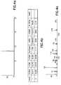
- FIG. 4(a)is a gas chromatography (GC) spectrum for such ethylmethylaminotriisopropylgermane product
- FIG. 4(b)is a corresponding tabulation of peak data for such GC spectrum
- FIG. 4(c)is a mass spectrum for the ethylmethylaminotriisopropylgermane product
- FIG. 4(d)shows the nuclear magnetic resonance spectrum of i Pr 3 GeNEtMe.
- FIG. 5is an STA spectrum of the ethylmethylaminotriisopropylgermane product, showing differential scanning calorimetry (DSC) data and thermogravimetric (TG) data, as a function of temperature.
- DSCdifferential scanning calorimetry
- TGthermogravimetric
- FIG. 6is an Arrhenius plot of deposition rate, in A/min, as a function of inverse Kelvin temperature, showing the improvement in Ge deposition with ammonia co-reactant.
- FIG. 7is a plot of deposition rate, in A/min, as a function of volume percent ammonia introduced in the deposition operation.
- FIG. 8is a schematic representation of a schematic of a GST device structure.
- the present inventionrelates to antimony and germanium precursors useful for CVD/ALD of corresponding metal-containing thin films, to compositions including such precursors, methods of making such precursors, and films and microelectronic device products manufactured using such precursors, as well as corresponding manufacturing methods.
- the inventionrelates in one aspect to new classes of antimony precursors, of the following formulae (A), (B) and (C): Sb(NR 1 R 2 )(R 3 N(CR S R 6 ) m NR 4 ) (A) wherein:
- the inventionin another aspect relates to germanyl and silyl antimony precursors of formula (D): (R 4 ) n Sb(E(R 1 R 2 R 3 )) 3-n (D) wherein:
- the foregoing precursorsmay be usefully employed for CVD and ALD of Sb, Sb/Ge, Sb/Te and GST films.
- Such precursorsmay also be used in low temperature deposition applications with reducing co-reactants such as hydrogen, hydrogen plasma, amines, imines, hydrazines, silanes, silyl chalcogenides (e.g., (Me 3 Si) 2 Te), germanes (e.g., GeH 4 ), ammonia, alkanes, alkenes and alkynes.
- reducing co-reactantssuch as hydrogen, hydrogen plasma, amines, imines, hydrazines, silanes, silyl chalcogenides (e.g., (Me 3 Si) 2 Te), germanes (e.g., GeH 4 ), ammonia, alkanes, alkenes and alkynes.
- suitable solventsinclude alkanes (e.g., hexane, heptane, octane and pentane), aryl solvents (e.g., benzene, toluene), amines (e.g., triethylamine, tert-butylamine), imines, hydrazines and ethers.
- alkanese.g., hexane, heptane, octane and pentane
- aryl solventse.g., benzene, toluene
- aminese.g., triethylamine, tert-butylamine
- imineshydrazines and ethers.
- a solid delivery systemmay be utilized for delivery of the antimony precursor, such as for example the ProE-Vap® solid delivery and vaporizer system commercially available from ATMI, Inc., Danbury, Connecticut, USA.
- antimony precursors of the inventioncan be "fine-tuned" by choice of appropriate substituents, within the broad formulae set out hereinabove, to provide desired characteristics of thermal stability, volatility and compatibility with other co-reagents or components in a multi-component precursor system.
- antimony precursors of the inventionare readily synthesized, by synthetic routes including those described below.
- the antimony precursor of the general formula (A):can for example be synthesized according to the following reaction scheme (A): SbX 3 + Li(NR 1 R 2 ) + Li(R 3 N(CR 5 R 6 ) m NR 4 ) ⁇ and the antimony precursor of the general formula (B): can be synthesized according to the following reaction scheme (B): SbX 3 + R 1 MgX + Li(R 2 N(CR 4 R 5 ) m NR 3 ) ⁇ or by the following reaction scheme (C): SbX 3 + mR 2 (CR 4 R 5 ) R 3 NSiMe 3 ⁇
- the antimony precursor of the general formula (C)can be formed by synthesis in a corresponding manner.
- the antimony precursor of the general formula (D), having the following structure:can for example be synthesized according to the following reaction schemes (D), when n is zero, or (E), when n is 2: wherein X is halo (fluorine, bromine, chlorine, iodine).
- RMgX and RLican be used as alternative synthesis reagents.
- FIG. 1shows the nuclear magnetic resonance spectrum of Sb(NMeEt) 3 and FIG. 2 shows the nuclear magnetic resonance spectrum of Sb(NMe 2 ) 3 .
- FIG. 3is a simultaneous thermal analysis (STA) graph for these two precursors, Sb(NMeEt) 3 and Sb(NMe 2 ) 3 , in which percentage thermogravimetry (TG) is plotted as a function of temperature, in degrees Centigrade.
- STAsimultaneous thermal analysis
- the inventionin another aspect relates to germanium precursors useful for CVD and ALD deposition of germanium films on substrates, of the following formulae I-XVI: wherein:
- germanium precursorscan variously be carried out in a ready manner, utilizing synthetic preparations of the types variously shown below.
- RMgCl, RMgBr, RMgI, RLi, and RNacan be used as alternative reagents.
- GeBr 4can be used in place of GeCl 4 ;
- LiNR 2can be replaced by NaNR 2 or KNR 2 ;
- Na(C 5 R 5 )can be used as an alternative to K(C 5 R 5 ).
- a multi-step synthetic approachmay be employed to generate mixed alkyl species through oxidative addition to a Ge(II) complex to generate Ge(IV) precursors, as shown below: wherein:
- a tetraallylgermanium complexcan be formed from such tetrachlorogermanium starting material using a corresponding allyl Grignard reagent R*MgCl, wherein R* is allyl
- Ge(II) compoundsthat may be usefully employed for CVD or ALD of germanium-containing films include the following:
- dialkylaminoisopropylgermane precursorsare used for CVD/ALD formation of GST thin films.
- Such precursorsmay be synthesized by a reaction scheme such as that shown below: to form germanium complexes such as:
- Tetrakisamidogermanes and triisopropylamines useful for such applications and amenable to transport with a heated bubblerinclude, for example, Ge(NMe 2 ) 4 , Ge(NEtMe) 4 , Ge(NEt 2 ) 4 , iPr 3 GeCl, iPr 3 GeNMe 2 , iPr 3 GeNEtMe, and iPr 3 GeNEt 2 .
- the volatility of the germanium precursors of the inventioncan be readily measured by STA thermogravimetric technique (e.g., by determining material transport under atmospheric pressure in argon) and GC analysis.
- isopropyl substituentsare in many cases preferred over methyl groups due to the ability of the isopropyl substituents to undergo beta-hydrogen elimination, thereby facilitating low temperature decomposition processing of the germanium precursor, without producing significant carbon residue.
- Nitrogen containing germanium precursors of the inventionhave the intrinsic benefit in many applications of mediating some incorporation of nitrogen in final films.
- Si- and N-doped GST materialshave lower reset currents, thereby enabling a lower temperature phase-change to occur.
- various germane precursors of the inventionundergo hydrogermolysis coupling reactions to form Ge-Ge bonds, via the reaction R 3 GeNR' 2 + R 3 GeH ⁇ R 3 Ge-GeR 3 , to yield digermane CVD precursors enabling highly efficient Ge-containing film deposition to be achieved, in relation to mono-germane precursors.
- the germanium precursors of the inventioncan contain a wide variety of ligand species as moieties thereof.
- ligandsmay for example include, without limitation, allyl, benzyl, t-butyl, cylopentadienyl, hydride, phenyl, and alkyl.
- Bidentate aminese.g. N, N-dialkylethylenediamine can also be used.
- the germanium precursorscan be delivered in solution or suspension in a liquid delivery technique, using suitable solvent media, or may be delivered for vapor phase desposition of Ge-containing films by solid delivery techniques, e.g., as described hereinabove in respect of the antimony precursors of the invention.
- the Ge precursormay be deposited separately or in combination with other precursors, e.g., with Sb and Te complexes such as iPr 3 Sb, Sb(NR 2 ) 3 , iPr 2 Te and Te(NR 2 ) 2 to form GST films.
- Sb and Te complexessuch as iPr 3 Sb, Sb(NR 2 ) 3 , iPr 2 Te and Te(NR 2 ) 2 to form GST films.
- germanium precursor of the inventionis Ge(triisopropyl)(methylethylamide), referred to sometimes hereinafter as GePNEM.
- This precursorcan be employed to deposit germanium on a substrate at suitable deposition process conditions, e.g., deposition temperature in a range of from 300°C to 450°C, and at pressure ranging from subatmospheric to superatmospheric (e.g., in a range of from about 0.5 torr to 15 atmospheres or more).
- Table ISet out in Table I below is a listing of film deposition rate, in Angstroms/minute, at varying temperature and pressure conditions, for deposition of germanium on substrates from the GePNEM precursor, delivered to the substrate in a carrier gas flow of hydrogen gas at 200 standard cubic centimeters per minute.
- the inventioncontemplates a precursor mixture including germanium precursor, antimony precursor and tellurium precursor, wherein at least one of the germanium precursor and antimony precursor includes a precursor selected from among the metal complexes of formulae (A), (B), (C), (D) and (E)(I)-(XVI) described hereinabove.
- the inventioncontemplates additional classes of antimony precursors.
- antimony precursorsare suitable for use in forming GST films, in conjunction with the use of suitable germanium and tellurium precursors.
- antimony precursorsinclude those of formulae (F), (G), (H), (I), (J), (K), (L) and (M), as defined below:
- Antimony precursors of a general type within the foregoing classes (F)-(M)include precursors having the following structures, wherein the various "R" groups in these structures are not necessarily numbered in exact correspondence with the substituent numberings in the above formulae, but nonetheless reflect the substituted positions in general fashion, which will be understood in reference to the above definitions of the substituents at the various positions of the associated molecules.
- the antimony precursors of classes (F)-(M)are usefully employed for deposition of antimony at low temperature with reducing co-reactants, e.g., reactants such as hydrogen, H 2 /plasma, amines, imines, hydrazines, silanes, silyl chalcogenides such as (Me 3 Si) 2 Te, germanes such as GeH 4 , ammonia, alkanes, alkenes, and alkynes.
- reactantssuch as hydrogen, H 2 /plasma, amines, imines, hydrazines, silanes, silyl chalcogenides such as (Me 3 Si) 2 Te, germanes such as GeH 4 , ammonia, alkanes, alkenes, and alkynes.
- the antimony precursorsmay be delivered for such deposition via liquid delivery techniques, in which precursors that are liquids may be used in neat liquid form, and precursors that are solids or liquids may be delivered in solutions or suspensions, in combination with suitable solvents, such as alkane solvents (e.g., hexane, heptane, octane, and pentane), aryl solvents (e.g., benzene or toluene), amines (e.g., triethylamine, tert-butylamine), imines and hydrazines.
- suitable solventssuch as alkane solvents (e.g., hexane, heptane, octane, and pentane), aryl solvents (e.g., benzene or toluene), amines (e.g., triethylamine, tert-butylamine), imines and hydrazines.
- solid delivery techniquesmay be employed, in which the solid precursor is volatilized, to form a precursor vapor that is delivered to the deposition chamber for forming an antimony or antimony-containing film on the substrate.
- the solid precursormay be packaged for such use in a storage and dispensing package of suitable character, such as the ProE-Vap solid delivery and vaporizer unit commercially available from ATMI, Inc. (Danbury, CT, USA).
- the inventionalso contemplates the use of antimony, germanium and tellurium precursors of the present invention separately for deposition of antimony-containing films, germanium-containing films, and tellurium-containing films, respectively.
- an antimony precursor of the inventionmay be employed to deposit an antimony-containing film.
- a germanium precursor of the inventionmay be employed to form a germanium-containing film.
- a tellurium precursor of the inventionmay be employed to form a tellurium-containing film.
- an antimony precursor of the invention and a germanium precursor of the inventionmay be utilized to form an antimony/germanium film.
- an antimony precursor of the inventioncan be utilized in combination with a tellurium precursor, to form an antimony/tellurium film.
- Another embodiment of the inventioninvolves use of a germanium precursor of the invention in combination with a tellurium precursor, to form a germanium/tellurium film.
- the antimony and/or germanium precursors of the inventioncan be used to deposit Ge 2 Sb 2 Te 5 films on suitable microelectronic device substrates in the fabrication of phase change memory devices.
- Such GST filmscan be fabricated using continuous CVD or ALD techniques using suitable germanium, antimony and tellurium precursors, with at least one of the germanium and antimony precursors comprising a metal complex of the present invention.
- the precursorsmay be supplied in appropriate ratios to yield the GST film of desired character.
- ALDmay be performed with the precursors (Ge, Sb, Te) being pulsed in a manner to control composition of the resulting film, e.g., with a pulse cycle including a sequential introduction of precursor species in the sequence Te-Ge-Te-Sb-Te-Ge-Te-Sb-Te, repetitively conducted until a desired film thickness has been achieved.
- co-reactant speciesmay be added in the deposition operation, to compositionally modify the resulting film.
- co-reactantsto compositionally modify the film for oxygen and/or nitrogen incorporation, e.g., with very small amounts of N 2 O, O 2 and NO.
- atomic layer deposition (ALD) and rapid vapor deposition (RVD) techniquesmay be employed to deposit films containing antimony and/or germanium using precursors of the present invention.
- ALDatomic layer deposition
- RVDrapid vapor deposition
- a rapid surface catalyzed vapor depositionmay be employed using ALD, in which a first precursor vapor is contacted with the substrate to form a saturated surface layer of the precursor, followed by exposure to a second precursor vapor, and thereafter by exposure to a third precursor vapor, with inert gas purges being carried out between the respective precursor vapor contacting steps, in which at least one of the first, second and third precursors comprises an antimony and/or germanium precursor of the invention and, and in which the precursor contacting and intervening purge steps are repetitively conducted until a predetermined thickness of deposited film material has been achieved.
- the present inventioncontemplates a wide variety of antimony and germanium complexes that can be utilized to form corresponding Sb- and Ge-containing films.
- the precursor complexes and compositions of the inventionaccordingly can be varied in specific usage, and can comprise, consist, or consist essentially of specific metal source reagents, or such specific reagents and other precursor species. Further, it may be desirable in some applications to employ multiple precursor species of the invention, in combination with one another and/or together with other precursor species.
- the inventionalso contemplates specific structural definitions and/or specifications of precursor complexes in specific embodiments, and the exclusion of specific moieties, ligands and elemental species in specific embodiments.
- the alkyl substituentsmay exclude methyl.
- tetrakisdialkylamidogermanesmay be excluded in certain embodiments of the invention.
- germanyl and silyl antimony complexes of the inventiontrimethylgermanyl and trimethylsilyl species may for example be excluded.
- FIG. 4(a)is a gas chromatography (GC) spectrum for such ethylmethylaminotriisopropylgermane product
- FIG. 4(b)is a corresponding tabulation of peak data for such GC spectrum
- FIG. 4(c)is a mass spectrum for the ethylmethylaminotriisopropylgermane product
- FIG. 4(d)shows the nuclear magnetic resonance spectrum of the ethylmethylaminotriisopropylgermane product.
- FIG. 5is an STA spectrum of the ethylmethylaminotriisopropylgermane product, showing differential scanning calorimetry (DSC) data and thermogravimetric (TG) data, as a function of temperature.
- DSCdifferential scanning calorimetry
- TGthermogravimetric
- Another aspect of the inventionrelates to tellurium complexes with beta-diketiminate ligands, which overcome the problems that many tellurium precursors used in deposition applications are very oxygen-sensitive and light-sensitive, and have an unpleasant odor.
- base stabilization with beta-diketiminate ligandsa tellurium precursor is obtained of a highly stable character with improved handling and shelf life characteristics, reduced odor, and sufficient volatility for deposition applications.
- the tellurium diketiminate complexes of the inventioncan be used for CVD/ALD to form Te or Te-containing films. These compounds can be used in combination with Ge- and/or Sb-compounds to produce Te-Ge-, Te-Sb- or Ge-Sb-Te films in varied compositions.
- a general procedure to synthesize diketiminate ligandshas been described in the literature, but such procedure is disadvantageous, since very bulky aryl substituents on the coordinating nitrogen atoms are required.
- alkyl ligandsas iso-propyl, n-butyl, tert-butyl or amine-substituted alkyl groups, as for example ethylene-dimethylamine, can be advantageously used to produce superior tellurium diketiminate precursors for CVD/ALD applications.
- Smaller substituents on the nitrogen donor atomsprovide sufficient volatility to form good films at low temperature.
- the ligands Lcan be used as the lithium salt or in a free imine form to synthesize the desired Te complexes.
- the free imine form of the ligand Lcan be reacted with a tellurium organic compound such as TeMe 4 to produce the desired Te species LTeMe 3 by methane elimination.
- TeMe 4a tellurium organic compound
- the diketiminate ligandsprovide very effective base stabilization of the reactive metal center tellurium.
- the inventiontherefore provides a new class of Te complexes that provide greater stability and shelf life, while retaining sufficient volatility to form superior Te films via CVD/ALD at low temperatures.
- the tellurium complexes of the inventionhave the formulae (I) and (II): wherein R 1 , R 2 and R 3 they be the same as or different from one another, and each is independently selected from C 1 -C 6 alkyl, C 6 -C 10 aryl, silyl and C 1 -C 12 alkylamine (which includes both monoalkylamine as well as dialkylamine); and wherein R 1 , R 2 and R 3 they be the same as or different from one another, and each is independently selected from C 1 -C 6 alkyl, C 6 -C 10 aryl, silyl and C 1 -C 12 alkylamine (which includes both monoalkylamine as well as dialkylamine).
- beta-diketiminate ligandsmay for example be synthesized by the following procedure:
- the tellurium complexesthen can be synthesized by the following reaction:
- tellurium complexes of the inventionare usefully employed as CVD/ALD precursors for deposition of tellurium-containing thin films, e.g., by liquid injection of neat precursor material, or in organic solvent or by direct evaporation.
- the inventionin another aspect relates to germanium complexes and their use in CVD/ALD for forming germanium-containing films, e.g., GST films, wherein the germanium complexes are selected from among: wherein the R groups in the second formula may be the same as or different from one another, and each is independently selected from among H, C 1 -C 6 alkyl, C 6 -C 10 aryl, C 3 -C 8 cycloalkyl, heteroatom groups, and other organo groups.
- Another aspect of the inventionrelates to digermane and strained ring germanium precursors for CVD/ALD of germanium-containing thin films.
- Previously employed germanium precursorssuch as germane that have been used for forming GST (germanium-antimony-tellurium) films for phase change memory devices require very high temperature deposition conditions. This in turn makes it difficult to form a pure Ge 2 Sb 2 Te 5 phase material.
- the present inventionovercomes this deficiency in the provision of precursors having a high vapor pressure at ambient conditions, which are useful to deposit germanium-containing films at temperatures below 300°C.
- Germanium-germanium bondsare inherently weak ( ⁇ 188 kJ/mole) and become less stable with electron withdrawing substituents such as chlorine or NMe 2 . Such bonds can readily dissociate to form R 3 Ge radicals under UV photolysis or thermolysis, or by chemical oxidation using peroxides, ozone, oxygen or plasma.
- Commercially available digermanesinclude hydride, methyl, phenyl, or ethyl groups that require high temperatures for decomposition and the resulting films are often contaminated with carbon residues.
- germanium complexesusing as ligands isopropyl, isobutyl, benzyl, allyl, alkylamino, nitriles, or isonitriles to achieve complexes that enabled the deposition of pure germanium metal films at low temperatures.
- the inventioncontemplates strained-ring germanium complexes (e.g., germacyclobutane) that can undergo thermal ring opening to generate a diradical intermediate that readily dissociates to germylene fragments.
- the bond dissociation energy of the strained Ge-C bond(63 kcal/mol) is considerable lower than Ge-CH 3 (83 kcal/mol), thereby enabling lower temperature film deposition of germanium to be achieved, than has been achievable with the aforementioned conventional germanium precursors.
- germanium complexes of the inventioninclude those of formulae (I) - (III) below:
- the complexes (I)can be synthesized, by way of example, according to the following synthesis process: or by the following synthesis: or by a synthesis such as the following: or a synthesis procedure such as:
- the germanium complexes of formula (II)can be formed by the following illustrated procedure:
- Illustrative synthesis processes that can be employed for forming germanium complexes of formula (III)includes the following:
- the strained ring alkylgermanesare usefully employed as CVD/ALD precursors for forming germanium-containing thin films on substrates involving reactions such as those illustratively shown below. Strained ring alkylgermanes as CVD/ALD precursors for thin metal films
- Another aspect of the inventionrelates to a single-source precursor for germanium and tellurium, as useful in the formation of GST films.
- Such single-source of germanium telluride precursorsmay be used in combination with an antimony precursor for GST film formation, optionally with co-reactants as may be desirable to provide films of appropriate stoichiometry for a given application.
- the germanium telluride complexes of the inventionin one aspect include dialkylgermanetellurones.
- Suitable dialkylgermanetelluronescan be synthesized by oxidative addition reaction of germanium (II) dialkyls with elemental tellurium powder in a solvent medium such as tetrahydrofuran (THF). In some instances so it may be desirable to conduct the reaction in the absence of light, depending on the light-sensitivity of the product germanium-tellurium complex.
- An illustrative synthesis procedureis set out below:
- the single-source Ge-Te precursors of the inventioncan be advantageously used to facilitate lower temperature deposition processes or to increase GST film growth rates in specific applications.
- Germanium tellurides of the inventionin another embodiment, can be formed by the following synthesis procedure:
- germanium telluride complexescan be formed by the following synthesis process: or by the following generalized reactions: R 3 GeM + R' n EX ⁇ R 3 Ge-ER' n R 3 GeX + R' n EM ⁇ R 3 Ge-ER' n R 2 Ge-X + NaTeR' ⁇ R 3 Ge-TeR' wherein E is tellurium; M is Li, Na, or K, X is chlorine, bromine or iodine; and the R and R' groups may be the same as or different from one another, and each is independently selected from among H, C 1 -C 6 alkyl, C 6 -C 10 aryl, C 3 -C 8 cycloalkyl, heteroatom groups, and other organo groups.
- One Ge-Te complex of the inventionis: wherein each of the R substituents may be the same as or different from one another, and is independently selected from among H, C 1 -C 6 alkyl, C 6 -C 10 aryl, C 3 -C 8 cycloalkyl, heteroatom groups, and other organo groups.
- Another aspect of the present inventionrelates to highly unsymmetric germanium complexes based on amide ligands, which are useful for low temperature (below 300°C) deposition of a germanium-antimony-tellurium (Ge 2 Sb 2 Te 5 ) thin film by a CVD or ALD process.
- amide ligandswhich are useful for low temperature (below 300°C) deposition of a germanium-antimony-tellurium (Ge 2 Sb 2 Te 5 ) thin film by a CVD or ALD process.
- R 1 , R 2 , R 3 , R 4 , R 5 , R 6 and R 7may be the same as or different from one another, and each is independently selected from the group consisting of C 1 -C 6 alkyl, C 6 -C 10 aryl, silyl, alkylsilyl (e.g., trimethylsilyl), hydrogen and halogen, or wherein in lieu of -NR 5 R 6 , the substituent coordinated to the germanium central atom is instead selected from the group consisting of C 1 -C 6 alkyl, C 3 -C 8 cycloalkyl, C 6 -C 13 aryl, or halide.
- the precursors of formulae (I) and (II)can be delivered to the CVD or ALD chamber by liquid delivery techniques, in which the precursor is dissolved or suspended in a suitable solvent medium.
- solvent mediainclude solvents selected from among alkanes (e.g., hexane, heptane, octane and pentane), aromatics (e.g., benzene or toluene), or amines (e.g., triethylamine or tert-butylamine).
- the precursorscan also be delivered as neat liquids, or alternatively by solid delivery techniques, utilizing suitable packaging for volatilization and dispensing.
- One preferred solid delivery packageis the ProE-VapTM solid delivery and vaporizer unit, commercially available from ATMI, Inc. (Danbury, Connecticut, USA).
- germanium complexes of formulae (I) and (II)can be synthesized according to the following synthesis schemes, in illustrative embodiments.
- the inventionin another aspect relates to tellurium complexes in which the tellurium central atom is coordinated to a nitrogen atom, to constitute a Te-N ligand complex.
- Te-N ligand complexesare the following tellurium complexes: wherein R 1 , R 2 , R 3 , R 4 , R 5 , R 6 and Z may be the same as or different from one another, and each is independently selected from the group consisting of C 1 -C 6 alkyl, C 3 -C 8 cycloalkyl, C 6 -C 10 aryl, silyl, alkylsilyl (e.g., trimethylsilyl), hydrogen and halogen, and wherein x is an integer having a value of from 1 to 3.
- the inventionrelates to germanium precursors useful in phase change memory device fabrication based on chalcogenide materials that undergo a phase change upon heating and are read out as "0" or "1" based on their electrical resistivity, which changes whether the phase change material in the memory cell is in a crystalline or amorphous state.
- Chalcogenide materialscomprise a large number of binary, ternary, and quaternary alloys of a number of metals and metalloids, e.g., GeSbTe, GeSbInTe, and many others.
- Phase change memory devicesrequire relatively pure alloys, with well controlled composition.
- Current processesutilize physical vapor deposition to deposit thin films of these materials.
- CVD and ALD methodsare desirable for their inherent scalability to large area wafers and for composition control.
- a major deficiency in the current artis the high deposition temperature needed with current alkyl (e.g., Me 3 Sb, Me 2 Te) or halide sources, which typically greatly exceed 300°C and may be as high as 500°C, which exceeds the allowable thermal budget for device integration and can result in the evaporation of the chalcogenide material.
- current alkyle.g., Me 3 Sb, Me 2 Te
- halide sourcestypically greatly exceed 300°C and may be as high as 500°C, which exceeds the allowable thermal budget for device integration and can result in the evaporation of the chalcogenide material.
- the inventionin another aspect relates to various materials and processes that enable low temperature deposition of chalcogenide alloys.
- Such precursorscan enhance deposition at lower temperatures via beta hydrogen elimination.
- digermanesare employed to lower the incorporation temperature of germanium.
- Useful compounds in this respectinclude Ge 2 H 6 , Ge 2 Me 6 , or Ge 2 Et 6 .
- each of the R'scan be the same as or different from the others, and each is independently selected from among H, C 1 -C 8 alkyl, C 1 -C 8 fluroalkyl, C 6 -C 12 aryl, C 6 -C 12 fluoroaryl, C 3 -C 8 cyclo-alkyl, C 3 -C 8 cyclo-fluoroalkyl.
- Ge 2 R 4 compounds including Ge 2 Ph 4can be usefully employed for such purpose, wherein each of the R groups may be as above defined. Additional complexes may be utilized including 5-member ring complexes with Ge in the ring.
- Ge(II) complexesare also potentially useful in specific applications, such as cyclopentadienyl compounds of the formula Ge(CpR 5 ) 2 wherein Cp is cyclopentadienyl and each of the R's may be the same as or different from one another and each is independently selected as above.
- Another germanium compound that is usefully employed for phase change memory applicationsis Ge(CH(SiMe 3 )) 2 .
- the antimony component of GST filmscan be supplied from a precursor such as triphenylantimony, which is inexpensive and light-sensitive in character, and has utility in light/UV-activated deposition processes.
- Delivery approaches for precursor delivery to enable low temperature deposition of chalcogenide alloysinclude the use of separate bubblers for in each precursor for the phase change memory film, liquid injection of precursor mixtures as an approach to manage disparate volatility characteristics of the several precursors to enable delivery of precise volumetric flows at desired compositions, and the use of mixtures of neat liquid or precursor/solvent compositions, as respective techniques that may be useful in specific applications.
- Film deposition approaches for low temperature deposition of chalcogenide alloysinclude: the use of continuous CVD in thermal mode, optionally with reducing gases such as hydrogen; employment of pulsed or atomic layer deposition to separate the dose step from the co-reactant such as hydrogen plasma; employment of activation techniques such as UV or other light sources that are "tuned" to the precursor, with a light being continuous with the precursor dosing, or dosed separately to avoid gas-phase reactions; and use of alternative reductive co-reactants such as germane (GeH 4 ) advantageously dispensed from sub-atmospheric delivery systems, such as the SAGE@ dispensing package commercially available from ATMI, Inc. (Danbury, Connecticut, USA), for enhanced safety and reduced cost of ownership for the source gas for the deposition.
- reducing gasessuch as hydrogen
- pulsed or atomic layer depositionto separate the dose step from the co-reactant such as hydrogen plasma
- activation techniquessuch as UV or other light sources that are "tuned” to the precursor
- the inventionfurther aspect relates to a low-temperature germanium nitride deposition process using an aminidate-based precursor, as found to be effective in forming germanium nitride at low temperature.
- FIG. 6is an Arrhenius plot of deposition log rate, in A/min, as a function of 1/T, showing the improvement in Ge deposition with ammonia co-reactant for germanium methyl amidinate (GeMAMDN).
- the precursoryields an amorphous Ge film with a deposition rate of about 2A/min at 280°C.
- the co-reactantwas switched to ammonia, the deposition rate increased dramatically.
- a factor of 100 in deposition ratewas observed at around 240°C, and a deposition rate of 75 A/min was achieved at 200°C.
- the deposited thin filmturned transparent with ammonia co-reactant indicating the formation of germanium nitride.
- FIG. 7shows the dominating effect of ammonia co-reactant on the deposition rate.
- the inventionin a further aspect relates to N, S, O-heterocyclic germanium CVD/ALD precursors for deposition of germanium metal films at low temperature.
- Illustrative of such precursorsare [ ⁇ MeC(iPrN) 2 ⁇ 2 Ge], [ ⁇ Me 2 N(iPrN) 2 ⁇ 2 Ge], [ ⁇ nBuC(iPrN) 2 ⁇ 2 Ge], and [ ⁇ MeC(NCy) 2 ⁇ 2 Ge].
- the precursor [ ⁇ MeC(iPrN) 2 ⁇ 2 Ge]may be provided in a solution of toluene as a CVD precursor for germanium metal films.
- the inventionin such respect contemplates the use of Ge(II) and Ge(IV) precursors with the following ligands: amidinates, guanidinates, isoureates, diketonates, diketoiminates, diketiminates, carbamates, thiocarbamates, silyls, aminotroponiminate.
- Mixed ligand precursorsare also included with combinations of the above ligands, or in combination with alkyl, dialkylamino, hydrido, or halogen groups.
- germanium precursorscan be used alone to deposit metallic germanium films thermally or with a co-reactant, or with iPr 2 Te or other suitable tellurium precursors to deposit GeTe layers.
- suitable antimony precursorsmay be employed to form the ternary GST alloy.
- Co-reactant gases/liquids usefully employed with such precursorsinclude hydrogen, ammonia, plasma, alkylamines, silanes, and germanes.
- germanium precursors of the inventioninclude:
- the ALD/CVD precursors (1)-(8) described abovecan be prepared in liquid delivery formulations using a suitable solvent such as alkanes (e.g., hexane, heptane, octane, and pentane), aromatics (e.g., benzene or toluene), or amines (e.g., triethylamine, tert-butylamine).
- a suitable solventsuch as alkanes (e.g., hexane, heptane, octane, and pentane), aromatics (e.g., benzene or toluene), or amines (e.g., triethylamine, tert-butylamine).
- Precursorsmay also be delivered as neat liquids or as solids using a suitable solid delivery and vaporizer unit (such as the ProE-VapTM solid delivery and vaporizer unit commercially available from ATMI, Inc., Dan
- the inventionin a further aspect contemplates various metal silylamides useful for CVD and ALD deposition of thin films.
- the "oligomers" of the above-discussed monomers with the same emprical formulainclude [R5nM ⁇ N[(R1R2)Si(CH2)mSi(R3R4)] ⁇ ox-n]x or [R5nM ⁇ R4N[Si(R1R2 R3)] ⁇ ox-n]x where x is an integer having a value of 2, 3, etc.
- the inventionalso contemplates precursors with open-structured silazane ligands in which at least one of the Rs has a functional group such as amido, alkoxyl, siloxyl and thienyl: R5nM ⁇ (R4R5R6)SiN[Si(R1R2 R3)] ⁇ ox-n, and its corresponding guanidinates.
- oligomersof the above-discussed monomer with the same emprical formula include [R5nM ⁇ (R4R5R6)SiN[Si(R1R2 R3)] ⁇ ox-n]x where x is an integer having a value of 2, 3, etc.
- Each of R1, R2, R3, R4, R6 and R7 in the about formulaeis independently selected from among H, C1-C6 alkyl, C3-C10 cycloalkyl, C6-C10 aryl, -Si(R8)3 and -Ge(R8)3 wherein each R8 is independently selected from C1-C6 alkyl; and -Si(R9)3 wherein each R9 is independently selected from C1-C6 alkyl; when suitable, pendant ligands attached to the above-mentioned R1, R2, R3, R4, R6 and R7 include functional group(s) providing further coordination to the metal center, such as, for example, aminoalkyl, alkoxyalkyl, aryloxyalkyl, imidoalkyl, and acetylalkyl, wherein suitable groups in these classes include those of the following formulae: wherein each of R1-R4 is the same as or different from one another, with each being independently selected from among hydrogen and C1-C6
- each R5can be independently selected from among H, C1-C6 alkyl, C3-C6 cycloalkyl, C1-C6 alkoxy, -NR1R2, and -C(R3)3, -Si(R8)3 and -Ge(R8)3 wherein each R3 is independently selected from C1-C6 alkyl; and each of R8 and R8 is independently selected from H, C1-C6 alkyl, C5-C10 cycloalkyl, C6-C10 aryl, and -Si(R9)3 wherein each R4 is independently selected from C1-C6 alkyl.
- Mcan be any of the metals mentioned above (Ta, V, Ti, Nb, Pb, Ni, W, Ca, Ba, In, Y, La, Zr, Hf, Ir, Ru, Pt, Cr, Mo, Ge; Al, Si, Ga, Sc, V, Cr, Fe, Sb, lanthanides, Mn, Co, Ni, Zn, Cd, Te, Hg, Au, Cu, Ag, Sr, Ru) but not limited to them only; OX is the allowed oxidation state of the metal M; n is an integer having a value of from 0 to ox; and X is halogen.
- the above-described precursor materialscan be used as low temperature deposition precursors with reducing co-reactants such as hydrogen, H2/plasma, amines, imines, hydrazines, silanes, silyl chalcogenides such as (Me3Si)2Te, germanes such as GeH4, ammonia, alkanes, alkenes, amidines, guanidines, boranes and their derivatives/adducts and alkynes.
- reducing co-reactantssuch as hydrogen, H2/plasma, amines, imines, hydrazines, silanes, silyl chalcogenides such as (Me3Si)2Te, germanes such as GeH4, ammonia, alkanes, alkenes, amidines, guanidines, boranes and their derivatives/adducts and alkynes.
- the precursorsmay be employed in liquid delivery formulations, and the precursors that are liquids may be used in neat liquid form, with liquid or solid precursors being employed as desired in suitable solvents including alkane solvents (e.g., hexane, heptane, octane, and pentane), aryl solvents (e.g., benzene or toluene), amines (e.g., triethylamine, tert-butylamine), imines, guanidines, amidines and hydrazines.
- alkane solventse.g., hexane, heptane, octane, and pentane
- aryl solventse.g., benzene or toluene
- aminese.g., triethylamine, tert-butylamine
- iminese.g., triethylamine, tert-butyl
- All of such complexescan be synthesized from the corresponding alkali metal salts with metal halides or alkyls or mixed halides/alkyls/amides or from the direct reactions between tetraalkylguanidine with metal halides with the presence of HX absorbents such as NEt3.
- each of R1, R2, R3, R4, R6 and R7is independently selected from among H, C1-C6 alkyl, C3-C10 cycloalkyl, C6-C10 aryl, -Si(R8)3 and -Ge(R8)3 wherein each R8 is independently selected from C1-C6 alkyl; and -Si(R9)3 wherein each R9 is independently selected from C1-C6 alkyl; when suitable, pendant ligands attached to the above-mentioned R1, R2, R3, R4, R6 and R7 including functional group(s) providing further coordination to the metal center, such as, for example, aminoalkyl, alkoxyalkyl, aryloxyalkyl, imidoalkyl, and acetylalkyl, wherein suitable groups in these classes include those of the following formula: wherein each of R1-R4 is the same as or different from one another, with each being independently selected from among hydrogen and C1-
- each R5can be independently selected from among H, C1-C6 alkyl, C3-C6 cycloalkyl, C1-C6 alkoxy, -NR1R2, and -C(R3)3, -Si(R8)3 and -Ge(R8)3 wherein each R3 is independently selected from C1-C6 alkyl; and each of R8 and R8 is independently selected from H, C1-C6 alkyl, C5-C10 cycloalkyl, C6-C10 aryl, and -Si(R9)3 wherein each R4 is independently selected from C1-C6 alkyl.
- Mcan be any of the metals mentioned above (Ta, V, Ti, Nb, Pb, Ni, W, Ca, Ba, In, Y, La, Zr, Hf, Ir, Ru, Pt, Cr, Mo, Ge; Al, Si, Ga, Sc, V, Cr, Fe, Sb, lanthanides, Mn, Co, Ni, Zn, Cd, Te, Hg, Au, Cu, Ag, Sr, Ru) but not limited to them only; OX is the allowed oxidation state of the metal M; n is an integer having a value of from 0 to ox; and X is halogen.
- the above-described precursor materialscan be used as low temperature deposition precursors with reducing co-reactants such as hydrogen, H2/plasma, amines, imines, hydrazines, silanes, silyl chalcogenides such as (Me3Si)2Te, germanes such as GeH4, ammonia, alkanes, alkenes, amidines, guanidines, boranes and their derivatives/adducts and alkynes.
- reducing co-reactantssuch as hydrogen, H2/plasma, amines, imines, hydrazines, silanes, silyl chalcogenides such as (Me3Si)2Te, germanes such as GeH4, ammonia, alkanes, alkenes, amidines, guanidines, boranes and their derivatives/adducts and alkynes.
- the precursorsmay be employed in liquid delivery formulations, and the precursors that are liquids may be used in neat liquid form, with liquid or solid precursors being employed as desired in suitable solvents including alkane solvents (e.g., hexane, heptane, octane, and pentane), aryl solvents (e.g., benzene or toluene), amines (e.g., triethylamine, tert-butylamine), imines, guanidines, amidines and hydrazines.
- alkane solventse.g., hexane, heptane, octane, and pentane
- aryl solventse.g., benzene or toluene
- aminese.g., triethylamine, tert-butylamine
- iminese.g., triethylamine, tert-butyl
- All of such precursorscan be synthesized from the corresponding alkali metal salts with metal halides or alkyls or mixed halides/alkyls or from direct reactions between guanidines with metal halides with the presence of HX absorbents such as NEt3.
- the syntheses of the guanidinate ligandscan be done from the corresponding carbodiimides and primary amines.
- each R5can be independently selected from among H, C1-C6 alkyl, C3-C6 cycloalkyl, C1-C6 alkoxy, -NR1R2, and -C(R3)3, -Si(R8)3 and -Ge(R8)3 wherein each R3 is independently selected from C1-C6 alkyl; and each of R8 and R8 is independently selected from H, C1-C6 alkyl, C5-C10 cycloalkyl, C6-C10 aryl, and -Si(R9)3 wherein each R4 is independently selected from C1-C6 alkyl.
- Mcan be any of the metals mentioned above (Ta, V, Ti, Nb, Pb, Ni, W, Ca, Ba, In, Y, La, Zr, Hf, Ir, Ru, Pt, Cr, Mo, Ge; Al, Si, Ga, Sc, V, Cr, Fe, Sb, lanthanides, Mn, Co, Ni, Zn, Cd, Te, Hg, Au, Cu, Ag, Sr, Ru) but not limited to them only; OX is the allowed oxidation state of the metal M; n is an integer having a value of from 0 to ox; and X is halogen.
- the above-described precursor materialscan be used as low temperature deposition precursors with reducing co-reactants such as hydrogen, H2/plasma, amines, imines, hydrazines, silanes, silyl chalcogenides such as (Me3Si)2Te, germanes such as GeH4, ammonia, alkanes, alkenes, amidines, guanidines, boranes and their derivatives/adducts and alkynes.
- reducing co-reactantssuch as hydrogen, H2/plasma, amines, imines, hydrazines, silanes, silyl chalcogenides such as (Me3Si)2Te, germanes such as GeH4, ammonia, alkanes, alkenes, amidines, guanidines, boranes and their derivatives/adducts and alkynes.
- the precursorsmay be employed in liquid delivery formulations, and the precursors that are liquids may be used in neat liquid form, with liquid or solid precursors being employed as desired in suitable solvents including alkane solvents (e.g., hexane, heptane, octane, and pentane), aryl solvents (e.g., benzene or toluene), amines (e.g., triethylamine, tert-butylamine), imines, guanidines, amidines and hydrazines.
- alkane solventse.g., hexane, heptane, octane, and pentane
- aryl solventse.g., benzene or toluene
- aminese.g., triethylamine, tert-butylamine
- iminese.g., triethylamine, tert-butyl
- Ais akali metals
- Xis halogens
- oxis the allowed oxidation state of M.
- the inventionin a further aspect relates to a highly selective germanium deposition process. Although discussed herein with primary reference to germanium, this process has applicability to other film deposition applications in which the film deposition process is dependent on nucleation processes, e.g., ruthenium deposition.
- Phase Change Memoryis currently considered the leading contender for nonvolatile memory based on its potential to scale down for several generations.
- Integrated GST based PCM deviceshave been made in the form of a large, flat layer with "plug” electrodes.
- Metalorganic Chemical Vapor Deposition (MOCVD) processesare under development for making these films, as it will certainly be necessary to deposit them in 3D geometries as device geometries shrink. In future generations, it will be necessary to scale this operation down to make the entire phase change chalcogenide section a plug within a via of insulating material such as silicon oxide, silicon nitride or low k dielectric.
- FIG. 8is a schematic of a GST device structure showing the GST plug, top electrode, bottom electrode, interlayer dielectric and associated layers of the device. Since neither etching nor CMP of this material is well established, making such a plug is not trivial, since a fairly thick layer is needed in order to allow for the bulk phase change that stores information in the form of a resistivity change. It would be desirable to grow the material in a "bottom up" way only in the via, without coating the rest of the structure. In order for this to occur, the deposition process must be highly selective, growing quickly on the desired surfaces and slowly or not at all on others.
- PCM materialIt might also be desirable to have the PCM material have poor contact with sidewalls of the via so as to reduce thermal contact and crosstalk between adjacent cells. Thus it could be desirable to have different sticking coefficients and nucleation likelihood on different surfaces.
- Heatup from room temperaturewas fixed at 4 minutes in all experiments. This could explain the behavior observed above, with deposition rate increasing from a few A/min up to 1000 A/min in a 10-15 degree C window, and with the location of this window shiftable by tens of degrees based on the reactant gas and partial pressure of the gases present.
- depositionwas carried out on Si02 substrates, and on a piece of TiN which was first heated to 400 C in 8T of hydrogen before being cooled to deposition temperature over the course of 10 minutes.
- the resultsincluded a deposition rate at 280 C of about 3 A/min deposited on TiN that had been exposed to air then placed on a susceptor.
- the deposition ratewas closer to 0.3 A/min, an order of magnitude lower.
- deposition ratewas close to 600 A/min at 280 C, and the rate was substantially higher at low temperatures.
- the preheated substratewas the closest simulation of a standard manufacturing process, where a TiN or similar electrode would be deposited in one part of a cluster tool, after which the substrate would be transferred to the CVD deposition module without any air exposure.
- the 200:1 ratio between deposition rates on preheated TiN and Si02is sufficient to obtain a very high selectivity on any combination of surfaces like this one. It is expected that this ratio would increase still further with clean, "in situ" deposited TiN and Si02.
- the most straightforward potential benefit to the unique behavior of this precursorwas bottom up fill of the vias to make a plug of chalcogenide phase change memory material.
- the Ge initial layercan be used as a somewhat more favorable growth site for a complete suite of precursors to help prevent "seams" or voids in the plug.
- a more indirect benefitis creation of a semiconductor compatible nucleation surface for other nucleation sensitive materials.
- Ru metalis difficult to grow in a purely reducing atmosphere; it tends to need some oxygen in its vicinity, for most CVD precursors.
- This Ge precursorcan be used to form a nucleation layer on Si at the bottom of a trench or via so that a slightly oxidizing process can be used, since Ge does not bond as strongly to oxygen as Si does, or a reducing process which deposits more easily on clean metal could be used.
- This approachcan be extended to deposition of materials other than Ru, providing they have some surface chemistry sensitivity that can be exploited.
- a surface, metal, nitride and/or Gecan have its surface chemistry changed via reactant gases (for example from oxide to metal) in order to switch it on and off for purposes of deposition from this precursor.
- reactant gasesfor example from oxide to metal
- the Gecan then be used as a protective layer for further chemistry modifications, e.g., as a hard mask, a sacrificial layer, etc. This principle can be extended to other elements than Ge upon finding appropriate precursors with this strong sensitivity to surface and deposition temperature.
- N-coordinated germanium amidesN-coordinated germanium amides, amidinates, guanidinates, and N-heterocyclic germylenes.
- the described processis also applicable to metal-organic CVD or ALD precursors comprising a metal selected from Ge, Sb, Te, Be, Mg, Ti, V, Cr, Mn, Fe, Ni, Cu, Zn, Y, Zr, Nb, Mo, Ru, Rh, Pd, Ag, Cd, Hg, La, Hf, Ta, W, Re, Os, Ir, Pt, Au, Sn, Pb, As, P, Bi, Al, Ga, In, Tl, and Si, to which is bound at least one weakly coordinating ligand selected from among halogen, B-diketiminate, nitrile, isonitrile, aminotroponiminate, carbonyl, phosphido, imido, amine, pyridine, amidinate, guanidinate, nitrosyl
- the present inventioncontemplates metal precursors of the formula MA y B x wherein M is a metal selected from among Ge, Sb and Te, and A is a ligand selected from the group consisting of all ligands disclosed herein, and y + x equals the oxidation state on metal M.
Landscapes
- Chemical & Material Sciences (AREA)
- Organic Chemistry (AREA)
- Engineering & Computer Science (AREA)
- Manufacturing & Machinery (AREA)
- Materials Engineering (AREA)
- Mechanical Engineering (AREA)
- Metallurgy (AREA)
- Chemical Kinetics & Catalysis (AREA)
- General Chemical & Material Sciences (AREA)
- Inorganic Chemistry (AREA)
- General Physics & Mathematics (AREA)
- Condensed Matter Physics & Semiconductors (AREA)
- Physics & Mathematics (AREA)
- Computer Hardware Design (AREA)
- Microelectronics & Electronic Packaging (AREA)
- Power Engineering (AREA)
- Chemical Vapour Deposition (AREA)
- Semiconductor Memories (AREA)
- Organic Low-Molecular-Weight Compounds And Preparation Thereof (AREA)
Abstract
Description
- The present invention relates to antimony and germanium complexes useful for CVD/ALD of metal thin films, to compositions including such complexes and to processes for depositing metal films on substrates using such complexes and compositions.
- Antimonides have been utilized in infrared detectors, high-speed digital circuits, quantum well structures and recently as a critical component together with germanium (Ge) and tellurium (Te) in phase change chalcogenide nonvolatile memory technology utilizing germanium-antimony-tellerium (Ge2Sb2Te5) films.
- Phase-change random access memory (PRAM) devices based on Ge-Sb-Te (GST) thin films utilize a reversible transition from a crystalline state to an amorphous state associated with changes in resistivity of the film material. The film material itself for high-speed commercial manufacturing and performance reasons is desirably formed using techniques such as chemical vapor deposition (CVD) and atomic layer deposition (ALD).
- Despite their promise, there are substantial challenges facing the efforts being made to grow reproducible, high-quality antimonide, Sb2Te3 and GST films by CVD and atomic layer deposition ALD at low temperature. These challenges include the following:
- (1) a very limited number of antimony CVD/ALD precursors is currently available, most being alkyl-based compounds such as Me3Sb, Et3Sb, (iPr)3Sb and Ph3Sb or hydride-based compounds such as SbH3, and these precursors suffer from various deficiencies including low thermal stability, low volatility, synthetic difficulties and high delivery temperatures;
- (2) the compatibility of such currently available antimony precursors with germanium or tellurium precursors is undetermined as far as their ability to reproducibly grow microelectronic device quality GST films, and the growth of antimonide films has associated process difficulties, including sensitivity to the V/III ratio and decomposition temperature; and
- (3) the deposited metal films formed from such precursors are susceptible to carbon or heteroatom contamination deriving from the precursor that can result in low growth rates, poor morphology and compositional variations in the films.
- Similar issues are encountered in the availability and selection of suitable germanium precursors for deposition of GST films, and in the use of germanium precursors for forming epitaxially grown strained silicon films, e.g., SiGe films.
- Germane (GeH4) is conventionally used to form germanium films but requires deposition temperatures above 500°C as well as rigorous safety controls and equipment. Other available Ge precursors require temperatures above 350°C for deposition of Ge films, or otherwise exhibit insufficient vapor pressures for transport or produce low film growth rates. Ideally, the germanium precursor can be used in CVD/ALD processes at low temperatures, on the order of 300°C and below, to form GST alloy thin films at high deposition rates, and with low carbon impurity levels in the resulting films.
- In consequence, the art continues to seek new antimony and germanium precursors for use in deposition of corresponding metal and metal alloy films by CVD and ALD techniques.
- The present invention relates to antimony and germanium precursors useful for CVD/ALD of corresponding metal-containing thin films, to compositions including such precursors, methods of making such precursors, and films and microelectronic device products manufactured using such precursors, as well as corresponding manufacturing methods.
- In one aspect, the invention relates to a metal complex selected from among complexes of formulae (A), (B), (C), (D) and (E)(I)-(E)(XVI):
Sb(NR1R2)(R3N(CR5R6)mNR4) (A)
wherein: - R1, R2, R3, and R4 may be the same as or different from one another, and are independently selected from C1-C6 alkyl, C3-C6 cycloalkyl, C2-C6 alkenyl (e.g., vinyl, allyl, etc.), C3-C6 alkylsilyl, C6-C10 aryl,
- each of R5 and R6 may be the same as or different from one another and are independently selected from hydrogen, C1-C6 alkyl, C3-C6 cycloalkyl, C2-C6 alkenyl (e.g., vinyl, allyl, etc.), C3-C6 alkylsilyl, and C6-C10 aryl; and
- m is an integer from 1 to 4 inclusive;-
Sb(R1)(R2N(CR4R5)mNR3) (B) - R1, R2, and R3 may be the same as or different from one another, and are independently selected from C1-C6 alkyl, C3-C6 cycloalkyl, C2-C6 alkenyl (e.g., vinyl, allyl, etc.), C3-C6 alkylsilyl, and C6-C10 aryl;
- each of R4 and R5 may be the same as or different from one another and is independently selected from hydrogen, C1-C6 alkyl, C3-C6 cycloalkyl, C2-C6 alkenyl (e.g., vinyl, allyl, etc.), C3-C6 alkylsilyl, and C6-C10 aryl; and
- m is an integer from 1 to 4 inclusive;
Sb(R1)3-n(NR2R3)n (C) - R1, R2 and R3 may be the same as or different from one another and are independently selected from hydrogen, C1-C6 alkyl, C3-C6 cycloalkyl, C2-C6 alkenyl (e.g., vinyl, allyl, etc.), silyl, C3-C6 alkylsilyl, C6-C10 aryl and -NR4R5, wherein each of R4 and R5 is selected from among H and C1-C4; and
- n is an integer from 0 to 3 inclusive;
(R4)nSb(E(R1R2R3))3-n (D) - R1, R2, R3, and R4 may be the same as or different from one another, and are independently selected from C1-C6 alkyl, C3-C6 cycloalkyl, C3-C6 alylsilyl, C6-C10 aryl, and alkylamino of the formula ―NR5R6 wherein each of R5 and R6 is independently selected from H and C1-C4 alkyl;
E is silicon (Si) or germanium (Ge); and
n is an integer from 0 to 3 inclusive;
(E) germanium precursors of the following formulae I-XVI:
- R1 and R2 may be the same as or different from one another, and are independently selected from H, C1-C6 alkyl, C2-C5 alkenyl, C5-C10 cycloalkyl, C6-C10 aryl, and -Si(R3)3 wherein each R3 is independently selected from C1-C6 alkyl;

- R and R' may be the same as or different from one another, and each R and R' is independently selected from H, C1-C6 alkyl, C2-C5 alkenyl, C5-C10 cycloalkyl, C6-C10 aryl, and -Si(R3)3 wherein each R3 is independently selected from C1-C6 alkyl;

- R, R', R1 and R2 may be the same as or different from one another, and each is independently selected from H, C1-C6 alkyl, C2-C5 alkenyl, C5-C10 cycloalkyl, C6-C10 aryl, and -Si(R3)3 wherein each R3 is independently selected from C1-C6 alkyl;
(R)4-nGe(NR1R2)n IV - R, R1 and R2 may be the same as or different from one another, and each is independently selected from H, C1-C6 alkyl, C2-C5 alkenyl, C5-C10 cycloalkyl, C6-C10 aryl, and -Si(R3)3 wherein each R3 is independently selected from C1-C6 alkyl; and
- n is an integer from 0 to 4 inclusive;

- R1, R2, R3, R4, R5 and R6 may be the same as or different from one another, and each is independently selected from H, C1-C6 alkyl, C2-C5 alkenyl, C5-C10 cycloalkyl, C6-C10 aryl, and -Si(R3)3 wherein each R3 is independently selected from C1-C6 alkyl;

- R is selected from H, C1-C6 alkyl, and C6-C10 aryl; and
- x is 0, 1 or 2;

- R1, R2, R3 and R4 may be the same as or different from the others, and each is independently selected from among H, C1-C6 alkyl, C5-C10 cycloalkyl, C6-C10 aryl, and -Si(R3)3 wherein each R3 is independently selected from C1-C6 alkyl;

- R1, R2, R3, R4, and R5 may be the same as or different from one another, and each is independently selected from among H, C1-C6 alkyl, silyl, -Si(R')3, C6-C10 cycloalkyl, C6-C10 aryl, -(CH2)xNR'R", and -(CH2)xOR"', wherein x = 1, 2 or 3, and R', R" and R"' may be the same as or different from one another, and each is independently selected from C1-C6 alkyl;

- R' and R" may be the same as or different from one another, and are independently selected from among H, C1-C6 alkyl, C5-C10 cycloalkyl, C6-C10 aryl, and -Si(R3)3 wherein each R3 is independently selected from C1-C6 alkyl; and
- each X is independently selected from among C1-C6 alkyl, C1-C6 alkoxy, ―NR1R2, and -C(R3)3, wherein each of R1, R2 and R3 is independently selected from H, C1-C6 alkyl, C5-C10 cycloalkyl, C6-C10 aryl, and -Si(R4)3 wherein each R4 is independently selected from C1-C6 alkyl;

- R1, R2, R3 and R4 may be same as or different from one another, and are independently selected from among H, C1-C6 alkyl, C5-C10 cycloalkyl, C6-C10 aryl, and -Si(R3)3 wherein each R3 is independently selected from C1-C6 alkyl;

- R1, R2, R3 and R4 may be the same as or different from one another, and are independently selected from among H, C1-C6 alkyl, C5-C10 cycloalkyl, C6-C10 aryl, and -Si(R3)3 wherein each R3 is independently selected from C1-C6 alkyl;

- R1, R2, R3 and R4 may be the same as or different from one another, and are independently selected from among H, C1-C6 alkyl, C5-C10 cycloalkyl, C6-C10 aryl, and -Si(R3)3 wherein each R3 is independently selected from C1-C6 alkyl;
R1TeR2 XIII - R1 and R2 may be the same as or different from one another, and are independently selected from among H, C1-C6 alkyl, C5-C10 cycloalkyl, C6-C10 aryl, and -Si(R3)3 wherein each R3 is independently selected from C1-C6 alkyl;
R1Te(NR2R3) XIV - R1, R2 and R3 may be the same as or different from one another, and are independently selected from among H, C1-C6 alkyl, C5-C10 cycloalkyl, C6-C10 aryl, and -Si(R3)3 wherein each R3 is independently selected from C1-C6 alkyl;
R1Te-TeR2 XV - R1 and R2 may be the same as or different from one another, and are independently selected from among H, C1-C6 alkyl, C5-C10 cycloalkyl, C6-C10 aryl, and -Si(R3)3 wherein each R3 is independently selected from C1-C6 alkyl; and
R1R2R3R4Ge XVI - R1, R2, R3, and R4 may be the same as or different from one another, and are independently selected from among H, C1-C6 alkyl, C5-C10 cycloalkyl, C6-C10 aryl, and -Si(R3)3 wherein each R3 is independently selected from C1-C6 alkyl.
- In another aspect, the invention relates to a vapor of an above-described metal complex.
- In another aspect, the invention relates to a precursor mixture including germanium precursor, antimony precursor and tellurium precursor, wherein at least one of the germanium precursor and antimony precursor includes a precursor selected from among the metal complexes of formulae (A), (B), (C), (D) and (E)(I)-(XVI) above.
- In a further aspect, the invention relates to precursor composition comprising a metal complex of the invention, in a solvent medium.
- A further aspect of the invention relates to method of depositing metal on a substrate, comprising contacting the substrate with precursor vapor comprising vapor of a metal complex of the invention.
- Additional aspects of the invention relate to methods of making the precursors of the invention.
- A further aspect of the invention relates to Sb(NMeEt)3, Sb(CH=CMe2)3 and Sb(CH2CH=CH2)3.
- In another aspect, the invention relates to a packaged precursor supply system comprising a package containing a metal complex of the invention.
- Yet another aspect of the invention relates to a germanium complex whose structure and properties are more fully discussed hereinafter.
- In another aspect, the invention relates to a method of depositing germanium on a substrate, comprising contacting the substrate with precursor vapor comprising vapor of a germanium (II) complex selected from among the following:

- Another aspect of the invention relates to a method of method of depositing germanium on a substrate, comprising contacting the substrate with precursor vapor comprising vapor of dialkylaminotriisopropylgermane.
- The invention also contemplates a precursor vapor comprising vapor of dialkylaminotriisopropylgermane, in another aspect of the invention.
- One aspect of the invention relates to a method of depositing germanium on a substrate, comprising contacting the substrate with a precursor vapor comprising vapor of a germanium complex including ligands selected from among allyl, benzyl, t-butyl, cylopentadienyl, hydride, phenyl, alkyl, bidentate amines and N, N-dialkylethylenediamine.
- Another aspect of the invention relates to forming a GST film on a substrate, comprising contacting the substrate with a precursor vapor comprising vapor of a germanium complex of the invention, vapor of an antimony complex, and vapor of a tellurium complex.
- Another aspect of the invention relates to a dialkylaminotriisopropylgermane complex, e.g., diethylaminotriisopropylgermane and ethylmethylaminotriisopropylgermane.
- A still further aspect of the invention relates to a method of forming a germanium-containing film on a substrate, comprising contacting the substrate with a precursor vapor comprising vapor of diethylaminotriisopropylgermane or ethylmethylaminotriisopropyl-germane.
- A still further aspect of the invention relates to a method of making a microelectronic device, comprising chemical vapor deposition or atomic layer deposition of a metal-containing film on a substrate from a precursor vapor comprising vapor of at least one precursor as described herein.
- Where a range of carbon numbers is provided herein, in description of a corresponding chemical moiety, it is understood that each intervening carbon number and any other stated or intervening carbon number value in that stated range, is encompassed within the invention, e.g., C1-C6 alkyl is understood as including methyl (C1), ethyl (C2), propyl (C3), butyl (C4), pentyl (C5) and hexyl (C6), and the chemical moiety may be of any conformation, e.g., straight-chain or branched, it being further understood that sub-ranges of carbon number within specified carbon number ranges may independently be included in smaller carbon number ranges, within the scope of the invention, and that ranges of carbon numbers specifically excluding a carbon number or numbers are included in the invention, and sub-ranges excluding either or both of carbon number limits of specified ranges are also included in the invention.
- As used herein, the term "film" refers to a layer of deposited material having a thickness below 1000 micrometers, e.g., from such value down to atomic monolayer thickness values. In various embodiments, film thicknesses of deposited material layers in the practice of the invention may for example be below 100, 10, or 1 micrometers, or in various thin film regimes below 200, 100, or 50 nanometers, depending on the specific application involved.
- It is noted that as used herein and in the appended claims, the singular forms "a", "and", and "the" include plural referents unless the context clearly dictates otherwise.
- Other aspects, features and embodiments of the invention will be more fully apparent from the ensuing disclosure and appended claims.
FIG. 1 shows the nuclear magnetic resonance spectrum of Sb(NMeEt)3.FIG. 2 shows the nuclear magnetic resonance spectrum of Sb(NMe2)3.FIG. 3 is a simultaneous thermal analysis (STA) graph for Sb(NMeEt)3 and Sb(NMe2)3, in which percentage thermogravimetry (TG) is plotted as a function of temperature, in degrees Centigrade.FIG. 4(a) is a gas chromatography (GC) spectrum for such ethylmethylaminotriisopropylgermane product, andFIG. 4(b) is a corresponding tabulation of peak data for such GC spectrum.FIG. 4(c) is a mass spectrum for the ethylmethylaminotriisopropylgermane product.FIG. 4(d) shows the nuclear magnetic resonance spectrum ofiPr3GeNEtMe.FIG. 5 is an STA spectrum of the ethylmethylaminotriisopropylgermane product, showing differential scanning calorimetry (DSC) data and thermogravimetric (TG) data, as a function of temperature.FIG. 6 is an Arrhenius plot of deposition rate, in A/min, as a function of inverse Kelvin temperature, showing the improvement in Ge deposition with ammonia co-reactant.FIG. 7 is a plot of deposition rate, in A/min, as a function of volume percent ammonia introduced in the deposition operation.FIG. 8 is a schematic representation of a schematic of a GST device structure.- The present invention relates to antimony and germanium precursors useful for CVD/ALD of corresponding metal-containing thin films, to compositions including such precursors, methods of making such precursors, and films and microelectronic device products manufactured using such precursors, as well as corresponding manufacturing methods.
- The invention relates in one aspect to new classes of antimony precursors, of the following formulae (A), (B) and (C):
Sb(NR1R2)(R3N(CRSR6)mNR4) (A)
wherein: - R1, R2, R3, and R4 may be the same as or different from one another, and are independently selected from C1-C6 alkyl, C3-C6 cycloalkyl, C2-C6 alkenyl (e.g., vinyl, allyl, etc.), C3-C6 alkylsilyl, C6-C10 aryl,
- each of R5 and R6 may be the same as or different from one another and are independently selected from hydrogen, C1-C6 alkyl, C3-C6 cycloalkyl, C2-C6 alkenyl (e.g., vinyl, allyl, etc.), C3-C6 alkylsilyl, and C6-C10 aryl; and
- m is an integer from 1 to 4 inclusive;-
Sb(R1)(R2N(CR4R5)mNR3) (B) - R1, R2, and R3 may be the same as or different from one another, and are independently selected from C1-C6 alkyl, C3-C6 cycloalkyl, C2-C6 alkenyl (e.g., vinyl, allyl, etc.), C3-C6 alkylsilyl, and C6-C10 aryl;
- each of R4 and R5 may be the same as or different from one another and is independently selected from hydrogen, C1-C6 alkyl, C3-C6 cycloalkyl, C2-C6 alkenyl (e.g., vinyl, allyl, etc.), C3-C6 alkylsilyl, and C6-C10 aryl; and
- m is an integer from 1 to 4 inclusive;
Sb(R1)3-n(NR2R3)n (C) - R1, R2 and R3 may be the same as or different from one another and are independently selected from hydrogen, C1-C6 alkyl, C3-C6 cycloalkyl, C2-C6 alkenyl (e.g., vinyl, allyl, etc.), silyl, C3-C6 alkylsilyl, C6-C10 aryl and -NR4R5, wherein each of R4 and R5 is selected from among H and C1-C4; and
- n is an integer from 0 to 3 inclusive.
- The invention in another aspect relates to germanyl and silyl antimony precursors of formula (D):
(R4)nSb(E(R1R2R3))3-n (D)
wherein: - R1, R2, R3, and R4 may be the same as or different from one another, and are independently selected from C1-C6 alkyl, C3-C6 cycloalkyl, C3-C6 alylsilyl, C6-C10 aryl, and alkylamino of the formula ―NR5R6 wherein each of R5 and R6 is independently selected from H and C1-C4 alkyl;
- E is silicon (Si) or germanium (Ge); and
- n is an integer from 0 to 3 inclusive.
- The foregoing precursors may be usefully employed for CVD and ALD of Sb, Sb/Ge, Sb/Te and GST films.
- Such precursors may also be used in low temperature deposition applications with reducing co-reactants such as hydrogen, hydrogen plasma, amines, imines, hydrazines, silanes, silyl chalcogenides (e.g., (Me3Si)2Te), germanes (e.g., GeH4), ammonia, alkanes, alkenes and alkynes.
- When specific precursors are in a liquid state, they may be used for liquid delivery in neat liquid form.
- Alternatively, when such precursors are in a liquid or solid state, they may be employed in suitable solvents, as a solution or suspension of the precursor. In specific applications, suitable solvents for such purpose include alkanes (e.g., hexane, heptane, octane and pentane), aryl solvents (e.g., benzene, toluene), amines (e.g., triethylamine, tert-butylamine), imines, hydrazines and ethers.
- The choice of a specific solvent composition for a particular antimony precursor or for a specific antimony precursor in combination with other germanium and tellurium precursors, may be readily determined, within the skill of the art based on the disclosure herein, to select an appropriate single component or multiple component solvent medium for liquid delivery vaporization and transport of the specific precursor component(s) involved.
- In various embodiments, where the antimony precursor is in a solid state, a solid delivery system may be utilized for delivery of the antimony precursor, such as for example the ProE-Vap® solid delivery and vaporizer system commercially available from ATMI, Inc., Danbury, Connecticut, USA.
- The antimony precursors of the invention can be "fine-tuned" by choice of appropriate substituents, within the broad formulae set out hereinabove, to provide desired characteristics of thermal stability, volatility and compatibility with other co-reagents or components in a multi-component precursor system.
- The antimony precursors of the invention are readily synthesized, by synthetic routes including those described below.
- The antimony precursor of the general formula (A):


SbX3 + Li(NR1R2) + Li(R3N(CR5R6)mNR4) →
and the antimony precursor of the general formula (B):
SbX3 + R1MgX + Li(R2N(CR4R5)mNR3) →
SbX3 + mR2(CR4R5) R3NSiMe3 →
- The antimony precursor of the general formula (C) can be formed by synthesis in a corresponding manner.
- The antimony precursor of the general formula (D), having the following structure:


- In the foregoing synthetic examples, RMgX and RLi can be used as alternative synthesis reagents.
- As specific examples illustrative of precursors of the invention, the precursors Sb(NMeEt)3, Sb(CH=CMe2)3, Sb(CH2CH=CH2)3 and Sb(NMe2)3 were synthesized and characterized. The precursors Sb(NMe2)3 and Sb(NMeEt)3 were determined to exhibit photosensitivity and therefore to require storage in a container protected from light exposure or in other photo-resistant packaging, to avoid light-induced decomposition thereof. Similar considerations are applicable to Sb(CH=CMe2)3 and Sb(CH2CH=CH2)3.
FIG. 1 shows the nuclear magnetic resonance spectrum of Sb(NMeEt)3 andFIG. 2 shows the nuclear magnetic resonance spectrum of Sb(NMe2)3.FIG. 3 is a simultaneous thermal analysis (STA) graph for these two precursors, Sb(NMeEt)3 and Sb(NMe2)3, in which percentage thermogravimetry (TG) is plotted as a function of temperature, in degrees Centigrade.- The invention in another aspect relates to germanium precursors useful for CVD and ALD deposition of germanium films on substrates, of the following formulae I-XVI:

- R1 and R2 may be the same as or different from one another, and are independently selected from H, C1-C6 alkyl, C2-C5 alkenyl, C5-C10 cycloalkyl, C6-C10 aryl, and -Si(R3)3 wherein each R3 is independently selected from C1-C6 alkyl;

- R and R' may be the same as or different from one another, and each R and R' is independently selected from H, C1-C6 alkyl, C2-C5 alkenyl, C5-C10 cycloalkyl, C6-C10 aryl, and -Si(R3)3 wherein each R3 is independently selected from C1-C6 alkyl;

- R, R', R1 and R2 may be the same as or different from one another, and each is independently selected from H, C1-C6 alkyl, C2-C5 alkenyl, C5-C10 cycloalkyl, C6-C10 aryl, and -Si(R3)3 wherein each R3 is independently selected from C1-C6 alkyl;
(R)4-nGe(NR1R2)n IV - R, R1 and R2 may be the same as or different from one another, and each is independently selected from H, C1-C6 alkyl, C2-C5 alkenyl, C5-C10 cycloalkyl, C6-C10 aryl, and -Si(R3)3 wherein each R3 is independently selected from C1-C6 alkyl; and
- n is an integer from 0 to 4 inclusive;

- R1, R2, R3, R4, R5 and R6 may be the same as or different from one another, and each is independently selected from H, C1-C6 alkyl, C2-C5 alkenyl, C5-C10 cycloalkyl, C6-C10 aryl, and -Si(R3)3 wherein each R3 is independently selected from C1-C6 alkyl;

- R is selected from H, C1-C6 alkyl, and C6-C10 aryl; and
- x is 0, 1 or 2;

- R1, R2, R3 and R4 may be the same as or different from the others, and each is independently selected from among H, C1-C6 alkyl, C5-C10 cycloalkyl, C6-C10 aryl, and -Si(R3)3 wherein each R3 is independently selected from C1-C6 alkyl;

- R1, R2, R3, R4, and R5 may be the same as or different from one another, and each is independently selected from among H, C1-C6 alkyl, silyl, -Si(R')3, C6-C10 cycloalkyl, C6-C10 aryl, -(CH2)xNR'R", and -(CH2)xOR"', wherein x = 1, 2 or 3, and R', R" and R"' may be the same as or different from one another, and each is independently selected from C1-C6 alkyl;

- R' and R" may be the same as or different from one another, and are independently selected from among H, C1-C6 alkyl, C5-C10 cycloalkyl, C6-C10 aryl, and -Si(R3)3 wherein each R3 is independently selected from C1-C6 alkyl; and
- each X is independently selected from among C1-C6 alkyl, C1-C6 alkoxy, ―NR1R2, and -C(R3)3, wherein each of R1, R2 and R3 is independently selected from H, C1-C6 alkyl, C5-C10 cycloalkyl, C6-C10 aryl, and -Si(R4)3 wherein each R4 is independently selected from C1-C6 alkyl;

- R1, R2, R3 and R4 may be same as or different from one another, and are independently selected from among H, C1-C6 alkyl, C5-C10 cycloalkyl, C6-C10 aryl, and -Si(R3)3 wherein each R3 is independently selected from C1-C6 alkyl;

- R1, R2, R3 and R4 may be the same as or different from one another, and are independently selected from among H, C1-C6 alkyl, C5-C10 cycloalkyl, C6-C10 aryl, and -Si(R3)3 wherein each R3 is independently selected from C1-C6 alkyl;

- R1, R2, R3 and R4 may be the same as or different from one another, and are independently selected from among H, C1-C6 alkyl, C5-C10 cycloalkyl, C6-C10 aryl, and -Si(R3)3 wherein each R3 is independently selected from C1-C6 alkyl;
R1TeR2 XIII - R1 and R2 may be the same as or different from one another, and are independently selected from among H, C1-C6 alkyl, C5-C10 cycloalkyl, C6-C10 aryl, and -Si(R3)3 wherein each R3 is independently selected from C1-C6 alkyl;
R1Te(NR2R3) XIV - R1, R2 and R3 may be the same as or different from one another, and are independently selected from among H, C1-C6 alkyl, C5-C10 cycloalkyl, C6-C10 aryl, and -Si(R3)3 wherein each R3 is independently selected from C1-C6 alkyl;
R1Te-TeR2 XV - R1 and R2 may be the same as or different from one another, and are independently selected from among H, C1-C6 alkyl, C5-C10 cycloalkyl, C6-C10 aryl, and -Si(R3)3 wherein each R3 is independently selected from C1-C6 alkyl; and
R1R2R3R4Ge XVI - R1, R2, R3, and R4 may be the same as or different from one another, and are independently selected from among H, C1-C6 alkyl, C5-C10 cycloalkyl, C6-C10 aryl, and -Si(R3)3 wherein each R3 is independently selected from C1-C6 alkyl.
- The synthesis of the above-described germanium precursors can variously be carried out in a ready manner, utilizing synthetic preparations of the types variously shown below. In each instance RMgCl, RMgBr, RMgI, RLi, and RNa can be used as alternative reagents. Further, GeBr4 can be used in place of GeCl4; LiNR2 can be replaced by NaNR2 or KNR2; and Na(C5R5) can be used as an alternative to K(C5R5). Moreover, a multi-step synthetic approach may be employed to generate mixed alkyl species through oxidative addition to a Ge(II) complex to generate Ge(IV) precursors, as shown below:

- R, R', and R" may be the same as or different from one another, and each is independently selected from H, C1-C6 alkyl, C2-C6 alkenyl, C5-C10 cycloalkyl, C6-C10 aryl, and -Si(R3)3 wherein each R3 is independently selected from C1-C6 alkyl, and M is Li, Na, MgCl, MgBr, or MgI.


- Illustrative Ge(II) compounds that may be usefully employed for CVD or ALD of germanium-containing films include the following:

- In various embodiments of the invention, dialkylaminoisopropylgermane precursors are used for CVD/ALD formation of GST thin films. Such precursors may be synthesized by a reaction scheme such as that shown below:


- The above-described germanium precursors are useful for CVD and ALD applications, to deposit germanium-containing films on substrates. Tetrakisamidogermanes and triisopropylamines useful for such applications and amenable to transport with a heated bubbler include, for example, Ge(NMe2)4, Ge(NEtMe)4, Ge(NEt2)4, iPr3GeCl, iPr3GeNMe2, iPr3GeNEtMe, and iPr3GeNEt2. The volatility of the germanium precursors of the invention can be readily measured by STA thermogravimetric technique (e.g., by determining material transport under atmospheric pressure in argon) and GC analysis.
- In specific embodiments of germanium precursors of the present invention containing alkyl substituents, isopropyl substituents are in many cases preferred over methyl groups due to the ability of the isopropyl substituents to undergo beta-hydrogen elimination, thereby facilitating low temperature decomposition processing of the germanium precursor, without producing significant carbon residue.
- Nitrogen containing germanium precursors of the invention have the intrinsic benefit in many applications of mediating some incorporation of nitrogen in final films. In this respect, Si- and N-doped GST materials have lower reset currents, thereby enabling a lower temperature phase-change to occur.
- As an additional advantage, various germane precursors of the invention undergo hydrogermolysis coupling reactions to form Ge-Ge bonds, via the reaction
R3GeNR'2 + R3GeH → R3Ge-GeR3,
to yield digermane CVD precursors enabling highly efficient Ge-containing film deposition to be achieved, in relation to mono-germane precursors. - The germanium precursors of the invention can contain a wide variety of ligand species as moieties thereof. Such ligands may for example include, without limitation, allyl, benzyl, t-butyl, cylopentadienyl, hydride, phenyl, and alkyl. Bidentate amines (e.g. N, N-dialkylethylenediamine) can also be used.
- The germanium precursors can be delivered in solution or suspension in a liquid delivery technique, using suitable solvent media, or may be delivered for vapor phase desposition of Ge-containing films by solid delivery techniques, e.g., as described hereinabove in respect of the antimony precursors of the invention.
- In use as CVD/ALD precursors, the Ge precursor may be deposited separately or in combination with other precursors, e.g., with Sb and Te complexes such as iPr3Sb, Sb(NR2)3, iPr2Te and Te(NR2)2 to form GST films.
- One illustrative germanium precursor of the invention is Ge(triisopropyl)(methylethylamide), referred to sometimes hereinafter as GePNEM. This precursor can be employed to deposit germanium on a substrate at suitable deposition process conditions, e.g., deposition temperature in a range of from 300°C to 450°C, and at pressure ranging from subatmospheric to superatmospheric (e.g., in a range of from about 0.5 torr to 15 atmospheres or more). Set out in Table I below is a listing of film deposition rate, in Angstroms/minute, at varying temperature and pressure conditions, for deposition of germanium on substrates from the GePNEM precursor, delivered to the substrate in a carrier gas flow of hydrogen gas at 200 standard cubic centimeters per minute.
Table I. Film Deposition Rate of Germanium Deposited at Varying Temperature and Pressure Conditions Temperature (°C) Temperature 1/T (K)Pressure 0.8 torr Pressure 8 torr 300 0.001745201 0.14 Å/min 0.35 Å/min 320 0.001686341 0.45 Å/min 340 0.001631321 1.32 Å/min 0.8 Å/min 360 0.001579779 1.48 Å/min 1.28 Å/min 380 0.001531394 2.4 Å/min 2.7 Å/min 400 0.001485884 3.4 Å/min 2.3 Å/min 420 0.001443001 6.8 Å/min 10.5 Å/min 440 0.001403 6.5 Å/min - In another determination of film thicknesses of germanium achieved by deposition from the GePNEM precursor, deposition carried out for a period of 16 minutes gave the following results: (i) temperature = 400°C, pressure = 800 millitorr, reactant gas H2, film thickness = 57 Å; (ii) temperature = 400°C, pressure = 800 millitorr, reactant gas NH3, film thickness = 94 Å; and (iii) temperature = 400°C, pressure = 8000 millitorr, reactant gas H2, film thickness = 36 Å. These results evidence the suitability of GePNEM for forming germanium or germanium-containing thin films on substrates by vapor deposition techniques.
- In various specific embodiments, the invention contemplates a precursor mixture including germanium precursor, antimony precursor and tellurium precursor, wherein at least one of the germanium precursor and antimony precursor includes a precursor selected from among the metal complexes of formulae (A), (B), (C), (D) and (E)(I)-(XVI) described hereinabove.
- In another aspect, the invention contemplates additional classes of antimony precursors. Such antimony precursors are suitable for use in forming GST films, in conjunction with the use of suitable germanium and tellurium precursors.
- Such additional classes of antimony precursors include those of formulae (F), (G), (H), (I), (J), (K), (L) and (M), as defined below:
- (F) aminidates, guanidates and isoureates of the formula:
R7nSb[R1NC(X)NR2]3-n
wherein:- where each R1 and R2 is independently selected from among H, C1-C6 alkyl, C5-C10 cycloalkyl, C6-C10 aryl, and -Si(R3)3 wherein each R3 is independently selected from C1-C6 alkyl; each X is independently selected from among C1-C6 alkoxy, ―NR4R5, and -C(R6)3, wherein each of R4, R5 and R6 is independently selected from H, C1-C6 alkyl, C5-C10 cycloalkyl, C6-C10 aryl, and -Si(R3)3 wherein each R3 is independently selected from C1-C6 alkyl;
- each R7 is independently selected from among C1-C6 alkoxy, ―NR8R9, and -C(R10)3, wherein each of R8, R9 and R10 is independently selected from H, C1-C6 alkyl, C5-C10 cycloalkyl, C6-C10 aryl, - Si(R3)3, and -Ge(R3)3 wherein each R3 is independently selected from C1-C6 alkyl; and
- n is an integer from 0 to 3;
- (G) tetra-alkyl guanidates of the formula:
R5nSb[(R1R2)NC(NR3R4)N)]3-n
wherein:- each of R1 and R2 is independently selected from among H, C1-C6 alkyl, C5-C10 cycloalkyl, C6-C10 aryl, and -Si(R9)3 wherein each R9 is independently selected from C1-C6 alkyl;
- each of R3 and R4 is independently selected from H, C1-C6 alkyl, C5-C10 cycloalkyl, C6-C10 aryl,
- and -Si(R9)3 wherein each R9 is independently selected from C1-C6 alkyl;
- each R5 is independently selected from among C1-C6 alkoxy, ―NR6R7, and -C(R8)3, wherein each of R6, R7 and R8 is independently selected from H, C1-C6 alkyl, C5-C10 cycloalkyl, C6-C10 aryl, - Si(R9)3, and -Ge(R9)3 wherein each R9 is independently selected from C1-C6 alkyl; and
- n is an integer from 0 to 3.
- (H) carbamates and thiocarbamates of the formula:
R4nSb[(EC(X)E]3-n
wherein:- each X is independently selected from among C1-C6 alkoxy, ―NR1R2, and -C(R3)3, wherein each of R1, R2 and R3 is independently selected from H, C1-C6 alkyl, C5-C10 cycloalkyl, C6-C10 aryl, and -Si(R5)3 wherein each R5 is independently selected from C1-C6 alkyl;
- each R4 is independently selected from among C1-C6 alkoxy, ―NR1R2, and -C(R3)3, wherein each of R1, R2 and R3 is independently selected from H, C1-C6 alkyl, C5-C10 cycloalkyl, C6-C10 aryl, and -Si(R5)3, -Ge(R5)3 wherein each R5 is independently selected from C1-C6 alkyl;
- E is either O or S; and
- n is an integer from 0 to 3;
- (I) beta-diketonates, diketoiminates, and diketiiminates, of the formulae:
[OC(R3)C(X)C(R2)O]3-nSb(R5)n
[OC(R3)C(X)C(R2)N(R1)]3-nSb(R5)n
[R4NC(R3)C(X)C(R2)N(R1)]3-nSb(R5)n
[(R3)OC(=O)C(X)C(R2)S]3-nSb(R5)n
where each of R1,R2, R3 and R4 is independently selected from among H, C1-C6 alkyl, C5-C10 cycloalkyl, C6-C10 aryl, and -Si(R6)3 wherein each R6 is independently selected from C1-C6 alkyl;
each X is independently selected from among C1-C6 alkoxy, -NR6R7, and -C(R8)3, wherein each of R6, R7 and R8 is independently selected from H, C1-C6 alkyl, C5-C10 cycloalkyl, C6-C10 aryl, and -Si(R6)3 wherein each R6 is independently selected from C1-C6 alkyl;
each R5 is independently selected from among guanidinate, aminidate, isoureate, allyl, C1-C6 alkoxy, -NR9R10, and -C(R11)3, wherein each of R9, R10 and R11 is independently selected from H, C1-C6 alkyl, C5-C10 cycloalkyl, C6-C10 aryl, -Si(R6)3, and -Ge(R6)3 wherein each R6 is independently selected from C1-C6 alkyl; and
n is an integer from 0 to 3. - (J) allyls of the formulae:
- (i): R4nSb[R1NC(X)C(R2R3)]3-n
- (ii): R4nSb[(R1O)NC(X)C(R2R3))3-n
- (iii): R4nSb[(R1R5)NC(X)C(R2R3))3-n
- (iv): R4Sb[(ONC(X)C(R2R3))]
each X is independently selected from among C1-C6 alkoxy, -NR1R2, and -C(R3)3, wherein each of R1, R2 and R3 is independently selected from H, C1-C6 alkyl, C5-C10 cycloalkyl, C6-C10 aryl, and -Si(R6)3 wherein each R6 is independently selected from C1-C6 alkyl;
each R4 is independently selected from among guanidinates, aminidates, isoureates, beta-diketonates, diketoiminates, diketiiminates, C1-C6 alkoxy, -NR7R8, and -C(R9)3, wherein each of R7, R8 and R9 is independently selected from H, C1-C6 alkyl, C5-C10 cycloalkyl, C6-C10 aryl, - Si(R6)3, and -Ge(R6)3 wherein each R6 is independently selected from C1-C6 alkyl; and
n is an integer from 0 to 3. - (L) cyclopentadienyl (Cp) antimony compounds wherein the Cp moiety is of the formulae:


wherein each of R1-R4 is the same as or different from one another, with each being independently selected from among hydrogen, C1-C6 alkyl, and C6-C10 aryl; R5 is selected from among C1-C6 alkyl, and C6-C10 aryl; and n and m are selected independently as having a value of from 0 to 4, with the proviso that m and n cannot be 0 at the same time;

n cannot be 0 at the same time;
wherein non-Cp ligand(s) of the antimony Cp compound can optionally include ligands selected from the group consisting of guanidinates, aminidates, isoureates, allyls, beta-diketonates, diketoiminates, and diketiiminates; and - (M) alkyls, alkoxides and silyls with pendent ligands, of the formulae:
- (i): R5nSb[(R1R2)N(CH2)mC(R1R2)3-n
- (ii): R5nSb[(R1R2)N(CH2)mSi(R1R2)3-n
- (iii): R5nSb[(R1R2)N(CH2)mO]3-n
- Antimony precursors of a general type within the foregoing classes (F)-(M) include precursors having the following structures, wherein the various "R" groups in these structures are not necessarily numbered in exact correspondence with the substituent numberings in the above formulae, but nonetheless reflect the substituted positions in general fashion, which will be understood in reference to the above definitions of the substituents at the various positions of the associated molecules.


- The antimony precursors of classes (F)-(M) are usefully employed for deposition of antimony at low temperature with reducing co-reactants, e.g., reactants such as hydrogen, H2/plasma, amines, imines, hydrazines, silanes, silyl chalcogenides such as (Me3Si)2Te, germanes such as GeH4, ammonia, alkanes, alkenes, and alkynes.
- The antimony precursors may be delivered for such deposition via liquid delivery techniques, in which precursors that are liquids may be used in neat liquid form, and precursors that are solids or liquids may be delivered in solutions or suspensions, in combination with suitable solvents, such as alkane solvents (e.g., hexane, heptane, octane, and pentane), aryl solvents (e.g., benzene or toluene), amines (e.g., triethylamine, tert-butylamine), imines and hydrazines. The utility of specific solvent compositions for particular antimony precursors can be readily empirically determined, to select an appropriate single component or multicomponent solvent medium for liquid delivery vaporization and transport of the specific antimony precursor that is employed.
- In another aspect of the invention, solid delivery techniques may be employed, in which the solid precursor is volatilized, to form a precursor vapor that is delivered to the deposition chamber for forming an antimony or antimony-containing film on the substrate. The solid precursor may be packaged for such use in a storage and dispensing package of suitable character, such as the ProE-Vap solid delivery and vaporizer unit commercially available from ATMI, Inc. (Danbury, CT, USA).
- The invention also contemplates the use of antimony, germanium and tellurium precursors of the present invention separately for deposition of antimony-containing films, germanium-containing films, and tellurium-containing films, respectively. Thus, an antimony precursor of the invention may be employed to deposit an antimony-containing film. In another embodiment, a germanium precursor of the invention may be employed to form a germanium-containing film. In another embodiment, a tellurium precursor of the invention may be employed to form a tellurium-containing film. In still another embodiment, an antimony precursor of the invention and a germanium precursor of the invention may be utilized to form an antimony/germanium film. In yet another embodiment, an antimony precursor of the invention can be utilized in combination with a tellurium precursor, to form an antimony/tellurium film. Another embodiment of the invention involves use of a germanium precursor of the invention in combination with a tellurium precursor, to form a germanium/tellurium film.
- The antimony and/or germanium precursors of the invention can be used to deposit Ge2Sb2Te5 films on suitable microelectronic device substrates in the fabrication of phase change memory devices.
- Such GST films can be fabricated using continuous CVD or ALD techniques using suitable germanium, antimony and tellurium precursors, with at least one of the germanium and antimony precursors comprising a metal complex of the present invention. The precursors may be supplied in appropriate ratios to yield the GST film of desired character. For example, ALD may be performed with the precursors (Ge, Sb, Te) being pulsed in a manner to control composition of the resulting film, e.g., with a pulse cycle including a sequential introduction of precursor species in the sequence Te-Ge-Te-Sb-Te-Ge-Te-Sb-Te, repetitively conducted until a desired film thickness has been achieved.
- As another variant of deposition techniques that may advantageously be employed to form films containing antimony and/or germanium, by use of precursors of the present invention, other co-reactant species may be added in the deposition operation, to compositionally modify the resulting film. Examples include use of co-reactants to compositionally modify the film for oxygen and/or nitrogen incorporation, e.g., with very small amounts of N2O, O2 and NO.
- In other embodiments, atomic layer deposition (ALD) and rapid vapor deposition (RVD) techniques may be employed to deposit films containing antimony and/or germanium using precursors of the present invention. For example, a rapid surface catalyzed vapor deposition may be employed using ALD, in which a first precursor vapor is contacted with the substrate to form a saturated surface layer of the precursor, followed by exposure to a second precursor vapor, and thereafter by exposure to a third precursor vapor, with inert gas purges being carried out between the respective precursor vapor contacting steps, in which at least one of the first, second and third precursors comprises an antimony and/or germanium precursor of the invention and, and in which the precursor contacting and intervening purge steps are repetitively conducted until a predetermined thickness of deposited film material has been achieved.
- More generally, the present invention contemplates a wide variety of antimony and germanium complexes that can be utilized to form corresponding Sb- and Ge-containing films. The precursor complexes and compositions of the invention accordingly can be varied in specific usage, and can comprise, consist, or consist essentially of specific metal source reagents, or such specific reagents and other precursor species. Further, it may be desirable in some applications to employ multiple precursor species of the invention, in combination with one another and/or together with other precursor species.
- The invention also contemplates specific structural definitions and/or specifications of precursor complexes in specific embodiments, and the exclusion of specific moieties, ligands and elemental species in specific embodiments. As an illustrative example, in homoleptic tris(dialkylamido)antimony complexes and tetrakis(dialkylamido)germanium complexes of the invention, the alkyl substituents may exclude methyl. As another example, tetrakisdialkylamidogermanes may be excluded in certain embodiments of the invention. As a still further example, in germanyl and silyl antimony complexes of the invention, trimethylgermanyl and trimethylsilyl species may for example be excluded. It will therefore be appreciated that the invention admits of delimited complexes and compositional features of complexes in various particularized embodiments of the invention, for purposes of identifying precursor complexes and classes of same that are preferred implementations of the invention in certain applications thereof.
- The synthesis of ethylmethylaminotriisopropylgermane is now described to show the details of making an illustrative germanium precursor of the invention.
- A solution of nBuLi (2M in hexanes, 26.34mL, 42.14mmol) was slowly added to an ice-cooled solution of ethylmethylamine (3.98mL, 46.35mmol) in ether (100mL). The resulting white mixture was stirred for 2 hours. Triisopropylchlorogermane (9.16mL, 42.14mmol) was added dropwise and the reaction mixture slowly warmed to room temperature. The mixture was stirred overnight, the solvent evaporated under vacuum, and the residue washed with pentane (100mL). The mixture was filtered through a medium glass frit under nitrogen and the solvent evaporated under vacuum to give 10.7g, 98% of a colorless liquid. The product was purified by fractional distillation (40°C, 75mtorr).1H NMR (C6D6): δ 2.87 (q, 2H,3J = 6.9Hz, NCH2CH3), 2.62 (s, 3H, NCH3), 1.36 (m, CH(CH3)2), 1.18 (d, 18H,3J = 7.2Hz, CH(CH3)2), 1.11 (t, 3H,3J = 6.9Hz, NCH2CH3)-13C NMR (C6D6): δ 48.42, 38.22 (NCH2CH3, NCH3), 20.19 (CH(CH3)2), 16.20, 15.79 (NCH2CH3, CH(CH3)2).
FIG. 4(a) is a gas chromatography (GC) spectrum for such ethylmethylaminotriisopropylgermane product, andFIG. 4(b) is a corresponding tabulation of peak data for such GC spectrum.FIG. 4(c) is a mass spectrum for the ethylmethylaminotriisopropylgermane product.FIG. 4(d) shows the nuclear magnetic resonance spectrum of the ethylmethylaminotriisopropylgermane product.FIG. 5 is an STA spectrum of the ethylmethylaminotriisopropylgermane product, showing differential scanning calorimetry (DSC) data and thermogravimetric (TG) data, as a function of temperature.- Another aspect of the invention relates to tellurium complexes with beta-diketiminate ligands, which overcome the problems that many tellurium precursors used in deposition applications are very oxygen-sensitive and light-sensitive, and have an unpleasant odor. By base stabilization with beta-diketiminate ligands, a tellurium precursor is obtained of a highly stable character with improved handling and shelf life characteristics, reduced odor, and sufficient volatility for deposition applications.
- The tellurium diketiminate complexes of the invention can be used for CVD/ALD to form Te or Te-containing films. These compounds can be used in combination with Ge- and/or Sb-compounds to produce Te-Ge-, Te-Sb- or Ge-Sb-Te films in varied compositions. A general procedure to synthesize diketiminate ligands has been described in the literature, but such procedure is disadvantageous, since very bulky aryl substituents on the coordinating nitrogen atoms are required.
- In contrast, we have discovered that smaller alkyl ligands as iso-propyl, n-butyl, tert-butyl or amine-substituted alkyl groups, as for example ethylene-dimethylamine, can be advantageously used to produce superior tellurium diketiminate precursors for CVD/ALD applications. Smaller substituents on the nitrogen donor atoms provide sufficient volatility to form good films at low temperature.
- The ligands L can be used as the lithium salt or in a free imine form to synthesize the desired Te complexes. The lithium salt of the ligand can be reacted with TeX4 (wherein X = Cl, Br, I) to generate LTeX3 by salt elimination, which can then be reacted with either a lithium or a Grignard reagent to produce LTeR3 (wherein R = alkyl, aryl, amide, silyl).
- Alternatively the free imine form of the ligand L can be reacted with a tellurium organic compound such as TeMe4 to produce the desired Te species LTeMe3 by methane elimination. The diketiminate ligands provide very effective base stabilization of the reactive metal center tellurium. The invention therefore provides a new class of Te complexes that provide greater stability and shelf life, while retaining sufficient volatility to form superior Te films via CVD/ALD at low temperatures.
- The tellurium complexes of the invention have the formulae (I) and (II):


- The beta-diketiminate ligands may for example be synthesized by the following procedure:

- The tellurium complexes then can be synthesized by the following reaction:

- or alternatively by the following synthesis reaction:

- or by the following synthesis reaction:

- The tellurium complexes of the invention are usefully employed as CVD/ALD precursors for deposition of tellurium-containing thin films, e.g., by liquid injection of neat precursor material, or in organic solvent or by direct evaporation.
- The invention in another aspect relates to germanium complexes and their use in CVD/ALD for forming germanium-containing films, e.g., GST films, wherein the germanium complexes are selected from among:

- Another aspect of the invention relates to digermane and strained ring germanium precursors for CVD/ALD of germanium-containing thin films. Previously employed germanium precursors such as germane that have been used for forming GST (germanium-antimony-tellurium) films for phase change memory devices require very high temperature deposition conditions. This in turn makes it difficult to form a pure Ge2Sb2Te5 phase material. The present invention overcomes this deficiency in the provision of precursors having a high vapor pressure at ambient conditions, which are useful to deposit germanium-containing films at temperatures below 300°C.
- Germanium-germanium bonds are inherently weak (∼ 188 kJ/mole) and become less stable with electron withdrawing substituents such as chlorine or NMe2. Such bonds can readily dissociate to form R3Ge radicals under UV photolysis or thermolysis, or by chemical oxidation using peroxides, ozone, oxygen or plasma. Commercially available digermanes include hydride, methyl, phenyl, or ethyl groups that require high temperatures for decomposition and the resulting films are often contaminated with carbon residues.
- We have overcome such deficiency by the provision of germanium complexes using as ligands isopropyl, isobutyl, benzyl, allyl, alkylamino, nitriles, or isonitriles to achieve complexes that enabled the deposition of pure germanium metal films at low temperatures. In addition, the invention contemplates strained-ring germanium complexes (e.g., germacyclobutane) that can undergo thermal ring opening to generate a diradical intermediate that readily dissociates to germylene fragments. The bond dissociation energy of the strained Ge-C bond (63 kcal/mol) is considerable lower than Ge-CH3 (83 kcal/mol), thereby enabling lower temperature film deposition of germanium to be achieved, than has been achievable with the aforementioned conventional germanium precursors.
- The germanium complexes of the invention include those of formulae (I) - (III) below:
- (I) alkyldigermanes of the formula

- (II) alkyl(dialkylamino)germanes of the formula
x(R2R1N)R3-xGe-GeR'3-y(NR1R2)y
wherein each R may be the same as or different from the others, and each is independently selected from among isopropyl, isobutyl, benzyl, allyl, alkylamino, nitriles, and isonitriles; and - (III) strained-ring germane complexes of the formula:

- The complexes (I) can be synthesized, by way of example, according to the following synthesis process:


- The germanium complexes of formula (II) can be formed by the following illustrated procedure:

- Illustrative synthesis processes that can be employed for forming germanium complexes of formula (III) includes the following:


- The strained ring alkylgermanes are usefully employed as CVD/ALD precursors for forming germanium-containing thin films on substrates involving reactions such as those illustratively shown below.
Strained ring alkylgermanes as CVD/ALD precursors for thin metal films

- Another aspect of the invention relates to a single-source precursor for germanium and tellurium, as useful in the formation of GST films. Such single-source of germanium telluride precursors may be used in combination with an antimony precursor for GST film formation, optionally with co-reactants as may be desirable to provide films of appropriate stoichiometry for a given application.
- The germanium telluride complexes of the invention in one aspect include dialkylgermanetellurones. Suitable dialkylgermanetellurones can be synthesized by oxidative addition reaction of germanium (II) dialkyls with elemental tellurium powder in a solvent medium such as tetrahydrofuran (THF). In some instances so it may be desirable to conduct the reaction in the absence of light, depending on the light-sensitivity of the product germanium-tellurium complex. An illustrative synthesis procedure is set out below:

- The single-source Ge-Te precursors of the invention can be advantageously used to facilitate lower temperature deposition processes or to increase GST film growth rates in specific applications.
- Germanium tellurides of the invention, in another embodiment, can be formed by the following synthesis procedure:
- Germanium telluride ALD/CVD precursors

- Other germanium telluride complexes can be formed by the following synthesis process:

R3GeM + R'nEX → R3Ge-ER'n
R3GeX + R'nEM → R3Ge-ER'n
R2Ge-X + NaTeR' → R3Ge-TeR'
wherein E is tellurium; M is Li, Na, or K, X is chlorine, bromine or iodine; and the R and R' groups may be the same as or different from one another, and each is independently selected from among H, C1-C6 alkyl, C6-C10 aryl, C3-C8 cycloalkyl, heteroatom groups, and other organo groups. - One Ge-Te complex of the invention is:

- Another aspect of the present invention relates to highly unsymmetric germanium complexes based on amide ligands, which are useful for low temperature (below 300°C) deposition of a germanium-antimony-tellurium (Ge2Sb2Te5) thin film by a CVD or ALD process. These complexes are selected from among complexes of formulae (I) and (II):


- The precursors of formulae (I) and (II) can be delivered to the CVD or ALD chamber by liquid delivery techniques, in which the precursor is dissolved or suspended in a suitable solvent medium. Illustrative of solvent media that may be employed in the broad practice of the present invention are solvents selected from among alkanes (e.g., hexane, heptane, octane and pentane), aromatics (e.g., benzene or toluene), or amines (e.g., triethylamine or tert-butylamine). The precursors can also be delivered as neat liquids, or alternatively by solid delivery techniques, utilizing suitable packaging for volatilization and dispensing. One preferred solid delivery package is the ProE-Vap™ solid delivery and vaporizer unit, commercially available from ATMI, Inc. (Danbury, Connecticut, USA).
- The germanium complexes of formulae (I) and (II) can be synthesized according to the following synthesis schemes, in illustrative embodiments.


- The invention in another aspect relates to tellurium complexes in which the tellurium central atom is coordinated to a nitrogen atom, to constitute a Te-N ligand complex.
- Illustrative of such Te-N ligand complexes are the following tellurium complexes:


- In another aspect, the invention relates to germanium precursors useful in phase change memory device fabrication based on chalcogenide materials that undergo a phase change upon heating and are read out as "0" or "1" based on their electrical resistivity, which changes whether the phase change material in the memory cell is in a crystalline or amorphous state. Chalcogenide materials comprise a large number of binary, ternary, and quaternary alloys of a number of metals and metalloids, e.g., GeSbTe, GeSbInTe, and many others.
- Phase change memory devices require relatively pure alloys, with well controlled composition. Current processes utilize physical vapor deposition to deposit thin films of these materials. CVD and ALD methods are desirable for their inherent scalability to large area wafers and for composition control. A major deficiency in the current art is the high deposition temperature needed with current alkyl (e.g., Me3Sb, Me2Te) or halide sources, which typically greatly exceed 300°C and may be as high as 500°C, which exceeds the allowable thermal budget for device integration and can result in the evaporation of the chalcogenide material.
- The invention in another aspect relates to various materials and processes that enable low temperature deposition of chalcogenide alloys.
- In one chemical approach, butyl and propyl (especially t-butyl and iso-propyl) substituted alkyl hydrides are employed as precursor complexes, e.g., complexes of the formula iPrxMHyy-x, wherein: x>1;, y = oxidation state of the metal (M) center; and y-x may = 0.
- In another chemical approach, butyl and propyl (especially t-butyl and iso-propyl) substituted alkyl halides are employed as precursor complexes, e.g., complexes of the formula iPrxMXy-x, wherein: X = F, Cl, Br; x>1; y = oxidation state of the metal (M) center; and y-x may = 0.
- Such precursors can enhance deposition at lower temperatures via beta hydrogen elimination.
- In another embodiment, digermanes are employed to lower the incorporation temperature of germanium. Useful compounds in this respect include Ge2H6, Ge2Me6, or Ge2Et6. Ge2iPr6 and Ge2tBu6, as well as Ge2(SiMe3)6 and Ge2Ph6, in which Me = methyl, Et = ethyl, iPr = isopropyl, tBu = t-butyl, and Ph = phenyl.
- More generally, compounds of the formula Ge2R6 may be employed, wherein each of the R's can be the same as or different from the others, and each is independently selected from among H, C1-C8 alkyl, C1-C8 fluroalkyl, C6-C12 aryl, C6-C12 fluoroaryl, C3-C8 cyclo-alkyl, C3-C8 cyclo-fluoroalkyl. In addition, Ge2R4 compounds including Ge2Ph4 can be usefully employed for such purpose, wherein each of the R groups may be as above defined. Additional complexes may be utilized including 5-member ring complexes with Ge in the ring. Ge(II) complexes are also potentially useful in specific applications, such as cyclopentadienyl compounds of the formula Ge(CpR5)2 wherein Cp is cyclopentadienyl and each of the R's may be the same as or different from one another and each is independently selected as above. Another germanium compound that is usefully employed for phase change memory applications is Ge(CH(SiMe3))2.
- In another aspect, the antimony component of GST films can be supplied from a precursor such as triphenylantimony, which is inexpensive and light-sensitive in character, and has utility in light/UV-activated deposition processes.
- Delivery approaches for precursor delivery to enable low temperature deposition of chalcogenide alloys include the use of separate bubblers for in each precursor for the phase change memory film, liquid injection of precursor mixtures as an approach to manage disparate volatility characteristics of the several precursors to enable delivery of precise volumetric flows at desired compositions, and the use of mixtures of neat liquid or precursor/solvent compositions, as respective techniques that may be useful in specific applications.
- Film deposition approaches for low temperature deposition of chalcogenide alloys include: the use of continuous CVD in thermal mode, optionally with reducing gases such as hydrogen; employment of pulsed or atomic layer deposition to separate the dose step from the co-reactant such as hydrogen plasma; employment of activation techniques such as UV or other light sources that are "tuned" to the precursor, with a light being continuous with the precursor dosing, or dosed separately to avoid gas-phase reactions; and use of alternative reductive co-reactants such as germane (GeH4) advantageously dispensed from sub-atmospheric delivery systems, such as the SAGE@ dispensing package commercially available from ATMI, Inc. (Danbury, Connecticut, USA), for enhanced safety and reduced cost of ownership for the source gas for the deposition.
- The invention further aspect relates to a low-temperature germanium nitride deposition process using an aminidate-based precursor, as found to be effective in forming germanium nitride at low temperature.
FIG. 6 is an Arrhenius plot of deposition log rate, in A/min, as a function of 1/T, showing the improvement in Ge deposition with ammonia co-reactant for germanium methyl amidinate (GeMAMDN). - With hydrogen co-reactant the precursor yields an amorphous Ge film with a deposition rate of about 2A/min at 280°C. When the co-reactant was switched to ammonia, the deposition rate increased dramatically. A factor of 100 in deposition rate was observed at around 240°C, and a deposition rate of 75 A/min was achieved at 200°C. Furthermore, the deposited thin film turned transparent with ammonia co-reactant indicating the formation of germanium nitride.
FIG. 7 shows the dominating effect of ammonia co-reactant on the deposition rate. - The invention in a further aspect relates to N, S, O-heterocyclic germanium CVD/ALD precursors for deposition of germanium metal films at low temperature. Illustrative of such precursors are [{MeC(iPrN)2}2Ge], [{Me2N(iPrN)2}2Ge], [{nBuC(iPrN)2}2Ge], and [{MeC(NCy)2}2Ge]. In a specific embodiment, the precursor [{MeC(iPrN)2}2Ge] may be provided in a solution of toluene as a CVD precursor for germanium metal films.
- In the formation of GST films, a high deposition rate, on the order of 400-500 A/min of GST alloy, and 100 A/min for Ge, along with low carbon and heteroatom impurity levels in the film, are required. Highly volatile precursors are necessary. Liquid precursors are preferred, however low melting and volatile solids may also be used with a heated bubbler system (∼ 50°C). Heteroatom impurities (Si, O, N) are acceptable below 10%.
- The invention in such respect contemplates the use of Ge(II) and Ge(IV) precursors with the following ligands: amidinates, guanidinates, isoureates, diketonates, diketoiminates, diketiminates, carbamates, thiocarbamates, silyls, aminotroponiminate. Mixed ligand precursors are also included with combinations of the above ligands, or in combination with alkyl, dialkylamino, hydrido, or halogen groups.
- The germanium precursors can be used alone to deposit metallic germanium films thermally or with a co-reactant, or with iPr2Te or other suitable tellurium precursors to deposit GeTe layers. Similarly, suitable antimony precursors may be employed to form the ternary GST alloy. Co-reactant gases/liquids usefully employed with such precursors include hydrogen, ammonia, plasma, alkylamines, silanes, and germanes.
- The germanium precursors of the invention include:
- (1) Ge(IV) amidinates, guanidinates, and isoureates of the formula:

each Z is independently selected from among C1-C6 alkoxy, -NR1R2, H, C1-C6 alkyl, C3-C10 cycloalkyl, C6-C13 aryl, and -Si(R4)3 wherein each R4 is independently selected from C1-C6 alkyl;
each Y group is independently selected from among C1-C6 alkoxy, -NR1R2, and C1-C6 alkyl, Si(R4)3, and halides (Cl, Br, I), and wherein x is integer from 0 to 4; - (2) Ge beta-diketonates, diketoiminates, diketiminates of the formulae:

- (3) Ge carbamates, thiocarbamates of the formulae:

- (4) Silylgermanes of the formula:

R4-xGe(TMS)x
(NRR')4-xGe(TMS)x
wherein TMS is Si(R")3; each R group is independently selected from among H, C1-C6 alkyl, C3-C10 cycloalkyl, C6-C12 aryl, and x is integer from 0 to 4; - (5) Mixed cyclopentadienyl germanes of the formulae:
R4-xGeCpx RGeCp
(RR'N)4-xGeCpx RR'NGeCp
CpGe(amidinate) CpGe(guanidinate)
CpGe(beta-diketiminate)
CpGe(beta-diketonate)
CpGe(isoureate)
wherein each R group is independently selected from among H, C1-C6 alkyl, C3-C10 cycloalkyl, C6-C13 aryl, and -Si(R')3 wherein each R' is independently selected from C1-C6 alkyl; and
each Y group is independently selected from among C1-C6 alkyl, C1-C6 alkoxy, NR1R2, C3-C10 cycloalkyl, C6-C13 aryl, Si(R4)3, and halides (Cl, Br, I), x is an integer having a value of from 0 to 4, and Cp ligands may also include:
- (6) Ge(II) amino-alkoxide of the formula:

n is an integer having a value of from 2 to 6; - (7) Other N-heterocyclic germylenes of the formulae:

each Y group is independently selected from among C1-C6 alkoxy, NR1R2, H, C1-C6 alkyl, C3-C10 cycloalkyl, C6-C13 aryl, Si(R4)3, or halides (Cl, Br, I); - (8) Oxides, dithiolates, thiocarbonates of the formulae:

- The ALD/CVD precursors (1)-(8) described above can be prepared in liquid delivery formulations using a suitable solvent such as alkanes (e.g., hexane, heptane, octane, and pentane), aromatics (e.g., benzene or toluene), or amines (e.g., triethylamine, tert-butylamine). Precursors may also be delivered as neat liquids or as solids using a suitable solid delivery and vaporizer unit (such as the ProE-Vap™ solid delivery and vaporizer unit commercially available from ATMI, Inc., Danbury, CT, USA).
- Set out below is an identification of various specific germanium precursors of the invention.


Ge(IV) precursors


- The invention in a further aspect contemplates various metal silylamides useful for CVD and ALD deposition of thin films.
- This aspect of the invention encompasses the synthesis and characterization of a class of metal precursors with disily-azacycloalkyl ligand: R5nM{N[(R1R2)Si(CH2)mSi(R3R4)]=ox-n; metal silylamides particularly with asymmetric elements in the silylamido ligands, R5nM{R4N[Si(R1R2 R3)]}ox-n; carbodiimido insertion reaction with those silylamides to yield the corresponding guanidinate complexes, which can also be used as CVD/ALD precursors.
- The "oligomers" of the above-discussed monomers with the same emprical formula include [R5nM{N[(R1R2)Si(CH2)mSi(R3R4)]}ox-n]x or [R5nM{R4N[Si(R1R2 R3)]}ox-n]x where x is an integer having a value of 2, 3, etc.
- The invention also contemplates precursors with open-structured silazane ligands in which at least one of the Rs has a functional group such as amido, alkoxyl, siloxyl and thienyl: R5nM{(R4R5R6)SiN[Si(R1R2 R3)]}ox-n, and its corresponding guanidinates.
- The "oligomers" of the above-discussed monomer with the same emprical formula include [R5nM{(R4R5R6)SiN[Si(R1R2 R3)]}ox-n]x where x is an integer having a value of 2, 3, etc.
- Each of R1, R2, R3, R4, R6 and R7 in the about formulae is independently selected from among H, C1-C6 alkyl, C3-C10 cycloalkyl, C6-C10 aryl, -Si(R8)3 and -Ge(R8)3 wherein each R8 is independently selected from C1-C6 alkyl; and -Si(R9)3 wherein each R9 is independently selected from C1-C6 alkyl; when suitable, pendant ligands attached to the above-mentioned R1, R2, R3, R4, R6 and R7 include functional group(s) providing further coordination to the metal center, such as, for example, aminoalkyl, alkoxyalkyl, aryloxyalkyl, imidoalkyl, and acetylalkyl, wherein suitable groups in these classes include those of the following formulae:


- In the metal precursors, each R5 can be independently selected from among H, C1-C6 alkyl, C3-C6 cycloalkyl, C1-C6 alkoxy, -NR1R2, and -C(R3)3, -Si(R8)3 and -Ge(R8)3 wherein each R3 is independently selected from C1-C6 alkyl; and each of R8 and R8 is independently selected from H, C1-C6 alkyl, C5-C10 cycloalkyl, C6-C10 aryl, and -Si(R9)3 wherein each R4 is independently selected from C1-C6 alkyl.
- In such metal precursors, M can be any of the metals mentioned above (Ta, V, Ti, Nb, Pb, Ni, W, Ca, Ba, In, Y, La, Zr, Hf, Ir, Ru, Pt, Cr, Mo, Ge; Al, Si, Ga, Sc, V, Cr, Fe, Sb, lanthanides, Mn, Co, Ni, Zn, Cd, Te, Hg, Au, Cu, Ag, Sr, Ru) but not limited to them only; OX is the allowed oxidation state of the metal M; n is an integer having a value of from 0 to ox; and X is halogen.
- The above-described precursor materials can be used as low temperature deposition precursors with reducing co-reactants such as hydrogen, H2/plasma, amines, imines, hydrazines, silanes, silyl chalcogenides such as (Me3Si)2Te, germanes such as GeH4, ammonia, alkanes, alkenes, amidines, guanidines, boranes and their derivatives/adducts and alkynes. The precursors may be employed in liquid delivery formulations, and the precursors that are liquids may be used in neat liquid form, with liquid or solid precursors being employed as desired in suitable solvents including alkane solvents (e.g., hexane, heptane, octane, and pentane), aryl solvents (e.g., benzene or toluene), amines (e.g., triethylamine, tert-butylamine), imines, guanidines, amidines and hydrazines.
- The utility of specific solvent compositions for particular precursors may be readily empirically determined, to select an appropriate single component or multiple component solvent medium for liquid delivery vaporization. Solid delivery systems may be employed, of the type previously described herein.
- The above-described precursors are variously shown below.


- The invention in a further aspect relates to tetraalkylguanidinate and ketiminate complexes useful as CVD and ALD precursors, including a class of metal precursors with tetraalkylguanidine ligand, e.g., in the coordination mode (R5)nM{N=C[(NR1R2)(NR3R4)]}ox-n and the semi-labile coordination mode. Under special circumstances, both coordination modes could theoretically co-exist.
- All of such complexes can be synthesized from the corresponding alkali metal salts with metal halides or alkyls or mixed halides/alkyls/amides or from the direct reactions between tetraalkylguanidine with metal halides with the presence of HX absorbents such as NEt3. The "oligomers" of such monomer with the same emprical formula include [(R5)nM{N=C[(NR1R2)(NR3R4)]}ox-n]x, where x is an integer having the value of 2, 3, etc.
- Four illustrative Ge (IV) precursors have been synthesized and characterized. All of them showed promising thermal behavior and TMG2Ge(NMe2)2 is a viscous liquid at room temperature.
- The invention also contemplates the corresponding guanidinate complexes R5nM{R6NC{N=C[(NR1R2)(NR3R4)]}NR7}ox-n. The "oligomers" of such monomer with the same emprical formula include [R5nM{R6NC{N=C[(NR1R2)(NR3R4)]}NR7}ox-n ]x, where x is an integer having the value of 2, 3, etc.
- The invention further encompasses a tetraalkylguanidine insertion reaction with metal amides to yield the corresponding guanidinate complexes, which can also be used as CVD/ALD precursors, as well as ketiminates of the formula (R5)nM{N=C[(R1R2)]}ox-n and its corresponding guanidinate complexes of the formula R5nM{R6NC[N=C(R1R2)]NR7}ox-n. The "oligomers" such monomer with the same emprical formula include [R5nM{R6NC[N=C(R1R2)]NR7}ox-n]x, where x is an integer having the value of 2, 3, etc.
- In the metal complexes described above, each of R1, R2, R3, R4, R6 and R7 is independently selected from among H, C1-C6 alkyl, C3-C10 cycloalkyl, C6-C10 aryl, -Si(R8)3 and -Ge(R8)3 wherein each R8 is independently selected from C1-C6 alkyl; and -Si(R9)3 wherein each R9 is independently selected from C1-C6 alkyl; when suitable, pendant ligands attached to the above-mentioned R1, R2, R3, R4, R6 and R7 including functional group(s) providing further coordination to the metal center, such as, for example, aminoalkyl, alkoxyalkyl, aryloxyalkyl, imidoalkyl, and acetylalkyl, wherein suitable groups in these classes include those of the following formula:


- In the metal precursors, each R5 can be independently selected from among H, C1-C6 alkyl, C3-C6 cycloalkyl, C1-C6 alkoxy, -NR1R2, and -C(R3)3, -Si(R8)3 and -Ge(R8)3 wherein each R3 is independently selected from C1-C6 alkyl; and each of R8 and R8 is independently selected from H, C1-C6 alkyl, C5-C10 cycloalkyl, C6-C10 aryl, and -Si(R9)3 wherein each R4 is independently selected from C1-C6 alkyl.
- In such metal precursors, M can be any of the metals mentioned above (Ta, V, Ti, Nb, Pb, Ni, W, Ca, Ba, In, Y, La, Zr, Hf, Ir, Ru, Pt, Cr, Mo, Ge; Al, Si, Ga, Sc, V, Cr, Fe, Sb, lanthanides, Mn, Co, Ni, Zn, Cd, Te, Hg, Au, Cu, Ag, Sr, Ru) but not limited to them only; OX is the allowed oxidation state of the metal M; n is an integer having a value of from 0 to ox; and X is halogen.
- The above-described precursor materials can be used as low temperature deposition precursors with reducing co-reactants such as hydrogen, H2/plasma, amines, imines, hydrazines, silanes, silyl chalcogenides such as (Me3Si)2Te, germanes such as GeH4, ammonia, alkanes, alkenes, amidines, guanidines, boranes and their derivatives/adducts and alkynes. The precursors may be employed in liquid delivery formulations, and the precursors that are liquids may be used in neat liquid form, with liquid or solid precursors being employed as desired in suitable solvents including alkane solvents (e.g., hexane, heptane, octane, and pentane), aryl solvents (e.g., benzene or toluene), amines (e.g., triethylamine, tert-butylamine), imines, guanidines, amidines and hydrazines.
- The utility of specific solvent compositions for particular precursors may be readily empirically determined, to select an appropriate single component or multiple component solvent medium for liquid delivery vaporization. Solid delivery systems may be employed, of the type previously described herein.
- The above-described precursors are variously shown below.


- Thermal and elemental analysis is set out in the table below, for the four illustrated precursors previously mentioned as having been characterized.

- The above-described precursors are variously shown below.
- The invention in a further aspect relates to dianionic chelate guanidinate ligands useful for CVD and ALD, and includes a class of metal precursors with dianionic chelate guanidine ligands of the formula (R4)nM{(R1)N=C[(NR2)(NR3)]}(ox-n)/2.
- All of such precursors can be synthesized from the corresponding alkali metal salts with metal halides or alkyls or mixed halides/alkyls or from direct reactions between guanidines with metal halides with the presence of HX absorbents such as NEt3. The syntheses of the guanidinate ligands can be done from the corresponding carbodiimides and primary amines.
- The "oligomers" of the above-claimed monomer with the same emprical formula include [(R4)nM{(R1)N=C[(NR2)(NR3)]}(ox-n)/2]x, where x is an integer having the value of 2, 3, etc., wherein each R1, R2, R3, R4, is independently selected from among H, C1-C6 alkyl, C3-C10 cycloalkyl, C6-C10 aryl, -Si(R5)3 and -Ge(R5)3 wherein each R8 is independently selected from C1-C6 alkyl; and -Si(R6)3 wherein each R9 is independently selected from C1-C6 alkyl; and when suitable, pendant ligands attached to the above-mentioned R1, R2, R3, R4 including functional group(s) providing further coordination to the metal center, such as, for example, aminoalkyl, alkoxyalkyl, aryloxyalkyl, imidoalkyl, and acetylalkyl, wherein suitable groups in these classes include those of the following formula:


- In the metal precursors, each R5 can be independently selected from among H, C1-C6 alkyl, C3-C6 cycloalkyl, C1-C6 alkoxy, -NR1R2, and -C(R3)3, -Si(R8)3 and -Ge(R8)3 wherein each R3 is independently selected from C1-C6 alkyl; and each of R8 and R8 is independently selected from H, C1-C6 alkyl, C5-C10 cycloalkyl, C6-C10 aryl, and -Si(R9)3 wherein each R4 is independently selected from C1-C6 alkyl.
- In such metal precursors, M can be any of the metals mentioned above (Ta, V, Ti, Nb, Pb, Ni, W, Ca, Ba, In, Y, La, Zr, Hf, Ir, Ru, Pt, Cr, Mo, Ge; Al, Si, Ga, Sc, V, Cr, Fe, Sb, lanthanides, Mn, Co, Ni, Zn, Cd, Te, Hg, Au, Cu, Ag, Sr, Ru) but not limited to them only; OX is the allowed oxidation state of the metal M; n is an integer having a value of from 0 to ox; and X is halogen.
- The above-described precursor materials can be used as low temperature deposition precursors with reducing co-reactants such as hydrogen, H2/plasma, amines, imines, hydrazines, silanes, silyl chalcogenides such as (Me3Si)2Te, germanes such as GeH4, ammonia, alkanes, alkenes, amidines, guanidines, boranes and their derivatives/adducts and alkynes. The precursors may be employed in liquid delivery formulations, and the precursors that are liquids may be used in neat liquid form, with liquid or solid precursors being employed as desired in suitable solvents including alkane solvents (e.g., hexane, heptane, octane, and pentane), aryl solvents (e.g., benzene or toluene), amines (e.g., triethylamine, tert-butylamine), imines, guanidines, amidines and hydrazines.
- The utility of specific solvent compositions for particular precursors may be readily empirically determined, to select an appropriate single component or multiple component solvent medium for liquid delivery vaporization. Solid delivery systems may be employed, of the type previously described herein.
- The above-described precursors are variously shown below.

- An exemplary ligand PriN=C(PriNH)2 was synthesized and characterized as follows.
- Example
- To a 250 mL flask charged with 12.6 g PriNCNPri (0.1 mol) and 100 ml tolune, 5.9 g PriNH2 (0.1 mol) was added at 0°C gradually. The resulting mixture was then refluxed at 100°C overnight. After work-up, 11.5 g solid PriN=C(PriNH)2 was obtained. (62% yield) Anal. Calcd for C10H23N3: C:64.81%: H:12.51%; N:22.68%. Found:C:64.73%: H:12.39%; N:22.48%.
- Selected bond lengths: [Å]
C(1)-N(3) 1.287(3)
C(1)-N(2) 1.358(3)
C(1)-N(1) 1.378(3) - The invention in a further aspect relates to a highly selective germanium deposition process. Although discussed herein with primary reference to germanium, this process has applicability to other film deposition applications in which the film deposition process is dependent on nucleation processes, e.g., ruthenium deposition.
- Phase Change Memory (PCM) is currently considered the leading contender for nonvolatile memory based on its potential to scale down for several generations. Integrated GST based PCM devices have been made in the form of a large, flat layer with "plug" electrodes. Metalorganic Chemical Vapor Deposition (MOCVD) processes are under development for making these films, as it will certainly be necessary to deposit them in 3D geometries as device geometries shrink. In future generations, it will be necessary to scale this operation down to make the entire phase change chalcogenide section a plug within a via of insulating material such as silicon oxide, silicon nitride or low k dielectric.
- An example of this can be seen in
FIG. 8 , which is a schematic of a GST device structure showing the GST plug, top electrode, bottom electrode, interlayer dielectric and associated layers of the device. Since neither etching nor CMP of this material is well established, making such a plug is not trivial, since a fairly thick layer is needed in order to allow for the bulk phase change that stores information in the form of a resistivity change. It would be desirable to grow the material in a "bottom up" way only in the via, without coating the rest of the structure. In order for this to occur, the deposition process must be highly selective, growing quickly on the desired surfaces and slowly or not at all on others. - It might also be desirable to have the PCM material have poor contact with sidewalls of the via so as to reduce thermal contact and crosstalk between adjacent cells. Thus it could be desirable to have different sticking coefficients and nucleation likelihood on different surfaces.
- It is also necessary to develop low temperature MOCVD processes for making these films, at temperatures of 300°C or less, since some components are volatile enough that stoichiometry control becomes difficult above this temperature.
- During our investigations of Ge precursors for PCMs, an amide-based precursor was discovered that has very strong selectivity based on surface state of the substrate on which it is being grown. This precursor, Ge(NMe2)4, undergoes a deposition rate change of close to 1000X over an extremely narrow temperature range, just 10-15°C. This is virtually unique behavior and we are aware of no other compound that does this.
- For such a strong effect to be taking place, it seemed likely that it was due to changes in the deposition surface and some kind of autocatalysis. These films were deposited on TiN, which was purchased commercially more than a year previously and cleaved into pieces for these experiments. Ti and TiN rapidly form oxides from exposure to atmosphere, and there is little doubt that the nucleation surface as inserted into the reactor was some form of Ti oxide or oxide nitride mix. Ti changes between various suboxides such as TiO2 and Ti2O3 readily, however, so it is possible that under reducing conditions such as the forming gas which flows through the reactor during heatup on the substrate, or even the hydrogen in which deposition takes place, the surface is altered in a fairly abrupt way at a particular transition temperature. Heatup from room temperature was fixed at 4 minutes in all experiments. This could explain the behavior observed above, with deposition rate increasing from a few A/min up to 1000 A/min in a 10-15 degree C window, and with the location of this window shiftable by tens of degrees based on the reactant gas and partial pressure of the gases present.
- In order to test this theory, deposition was carried out on Si02 substrates, and on a piece of TiN which was first heated to 400 C in 8T of hydrogen before being cooled to deposition temperature over the course of 10 minutes. The results included a deposition rate at 280 C of about 3 A/min deposited on TiN that had been exposed to air then placed on a susceptor. On a Si02 substrate, the deposition rate was closer to 0.3 A/min, an order of magnitude lower. Meanwhile, on the substrate which was preheated to 400 C then cooled in a reducing atmosphere in the reactor, deposition rate was close to 600 A/min at 280 C, and the rate was substantially higher at low temperatures. The preheated substrate was the closest simulation of a standard manufacturing process, where a TiN or similar electrode would be deposited in one part of a cluster tool, after which the substrate would be transferred to the CVD deposition module without any air exposure. The 200:1 ratio between deposition rates on preheated TiN and Si02 is sufficient to obtain a very high selectivity on any combination of surfaces like this one. It is expected that this ratio would increase still further with clean, "in situ" deposited TiN and Si02.
- The most straightforward potential benefit to the unique behavior of this precursor was bottom up fill of the vias to make a plug of chalcogenide phase change memory material. The Ge initial layer can be used as a somewhat more favorable growth site for a complete suite of precursors to help prevent "seams" or voids in the plug.
- If it were desirable, it might also be possible to have a plug of PCM material with poor contact to the side walls, providing better thermal isolation and less cross talk between adjacent PCM cells. Slow deposition and poor nucleation may lead to a poorly adhering layer with pores near the surface.
- A more indirect benefit is creation of a semiconductor compatible nucleation surface for other nucleation sensitive materials. For example, it is well known that Ru metal is difficult to grow in a purely reducing atmosphere; it tends to need some oxygen in its vicinity, for most CVD precursors. In addition, it is very hard to deposit it uniformly on a Si02 surface. This Ge precursor can be used to form a nucleation layer on Si at the bottom of a trench or via so that a slightly oxidizing process can be used, since Ge does not bond as strongly to oxygen as Si does, or a reducing process which deposits more easily on clean metal could be used. This approach can be extended to deposition of materials other than Ru, providing they have some surface chemistry sensitivity that can be exploited.
- In a more sophisticated approach, a surface, metal, nitride and/or Ge, can have its surface chemistry changed via reactant gases (for example from oxide to metal) in order to switch it on and off for purposes of deposition from this precursor. This in turn allows a chip surface that may have multiple materials exposed to have different surfaces switched on and off, depending on the layer material and coreactant, relative to Ge deposition. The Ge can then be used as a protective layer for further chemistry modifications, e.g., as a hard mask, a sacrificial layer, etc. This principle can be extended to other elements than Ge upon finding appropriate precursors with this strong sensitivity to surface and deposition temperature.
- Other chemicals and chemical families that may exhibit this behavior include N-coordinated germanium amides, amidinates, guanidinates, and N-heterocyclic germylenes. The described process is also applicable to metal-organic CVD or ALD precursors comprising a metal selected from Ge, Sb, Te, Be, Mg, Ti, V, Cr, Mn, Fe, Ni, Cu, Zn, Y, Zr, Nb, Mo, Ru, Rh, Pd, Ag, Cd, Hg, La, Hf, Ta, W, Re, Os, Ir, Pt, Au, Sn, Pb, As, P, Bi, Al, Ga, In, Tl, and Si, to which is bound at least one weakly coordinating ligand selected from among halogen, B-diketiminate, nitrile, isonitrile, aminotroponiminate, carbonyl, phosphido, imido, amine, pyridine, amidinate, guanidinate, nitrosyl, silyl, stibene (R3Sb), sulfide, and cyclopentadienyl.
- In a broad aspect, the present invention contemplates metal precursors of the formula MAyBx wherein M is a metal selected from among Ge, Sb and Te, and A is a ligand selected from the group consisting of all ligands disclosed herein, and y + x equals the oxidation state on metal M.
- While the invention has been has been described herein in reference to specific aspects, features and illustrative embodiments of the invention, it will be appreciated that the utility of the invention is not thus limited, but rather extends to and encompasses numerous other variations, modifications and alternative embodiments, as will suggest themselves to those of ordinary skill in the field of the present invention, based on the disclosure herein. Correspondingly, the invention as hereinafter claimed is intended to be broadly construed and interpreted, as including all such variations, modifications and alternative embodiments, within its spirit and scope.


each R5 is independently selected from among guanidinates, aminidates, isoureates, beta-diketonates, diketoiminates, diketiiminates, C1-C6 alkoxy, -NR6R7, and -C(R8)3, wherein each of R6, R7 and R8 is independently selected from H, C1-C6 alkyl, C5-C10 cycloalkyl, C6-C10 aryl, - Si(R3)3, and -Ge(R3)3 wherein each R3 is independently selected from C1-C6 alkyl;
n is an integer from 0 to 3;
m is integer from 0 to 4.


Claims (15)
- A vapor deposition process for depositing a germanium material on a substrate, wherein said process comprises volatilizing a germanium amidinate precursor to form a germanium-containing precursor vapor, and contacting the germanium-containing precursor vapor with the substrate at conditions effective for deposition, to deposit said germanium material on the substrate.
- The process of claim 1, wherein the germanium amidinate precursor includes (a) Ge(II) or Ge(IV), (b) at least one amidinate ligand of the formula [RNCXNR]- wherein each R is independently selected from H, C1-C6 alkyl, C3-C10 cycloalkyl, C6-C13 aryl, and -Si(R')3 wherein each R' is independently selected from C1-C6 alkyl, and X is selected from H, C1-C6 alkyl, C1-C6 alkoxy, -NR1R2, and -C(R3)3, wherein each of R1, R2 and R3 is independently selected from H, C1-C6 alkyl, C3-C10 cycloalkyl, C6-C13 aryl, and -Si(R4)3 wherein each R4 is independently selected from C1-C6 alkyl, and (c) optionally one or more non-amidinate ligand(s) selected from alkyl, alkoxy, dialkylamino, hydrido, -Si(R4)3 and halogen groups.
- The process of claim 1, wherein the germanium amidinate precursor comprises germanium bis(n-butyl, N,N-diisopropylamidinate).
- The process of any one of claims 1 to 3, wherein said contacting conditions comprise temperature of 300°C to 450°C.
- The process of any one of claims 1 to 4, wherein pressure in said contacting conditions comprise pressure of 0.5 Torr (66,66 Pa) to 15 atmospheres (1519875 Pa).
- The process of any of claims 1 to 5, comprising use of a reducing co-reactant in the contacting step.
- The process of claim 6, wherein the reducing co-reactant is selected from the group consisting of hydrogen, hydrogen plasma, alkanes, alkenes, amidines, guanidines, boranes and their adducts and derivatives, alkynes, alkylamines, silanes, silyl chalcogenides, germanes, ammonia, amines, imines, and hydrazines.
- The process of any one of claims 1 to 7, comprising chemical vapor deposition or atomic layer deposition of (i) the germanium material, and at least one of (ii) tellurium and (iii) antimony, on the substrate.
- The process of any one of claims 1 to 8, wherein the germanium amidinate precursor comprises germanium bis(n-butyl, N,N-diisopropylamidinate) in a precursor solution including a solvent.
- The process of any one of claims 1 to 9, wherein a co-reactant is used in the deposition to incorporate oxygen and/or nitrogen in the germanium material deposited on the substrate.
- The process of any one of claims 1 to 10, comprising doping the germanium material with silicon and nitrogen.
- The process of any one of claims 1 to 11, wherein the substrate comprises a microelectronic device substrate, and the germanium material is deposited in a via on the microelectronic device substrate, wherein the via is in a low k dielectric material comprising silicon oxide or silicon nitride.
- A precursor solution comprising germanium bis(n-butyl, N,N-diisopropylamidinate) and a solvent therefor.
- The precursor solution of claim 13, wherein the solvent is selected from the group consisting of alkane solvents, aryl solvents, amines, imines, guanidines, amidines, and hydrazines.
- The precursor solution of claim 13, wherein the solvent is selected from the group consisting of hexane, heptane, octane, pentane, benzene, toluene, triethylamine, and tert-butylamine.
Applications Claiming Priority (3)
| Application Number | Priority Date | Filing Date | Title |
|---|---|---|---|
| US86407306P | 2006-11-02 | 2006-11-02 | |
| US88724907P | 2007-01-30 | 2007-01-30 | |
| EP07758383AEP2078102B1 (en) | 2006-11-02 | 2007-03-12 | Antimony and germanium complexes useful for cvd/ald of metal thin films |
Related Parent Applications (1)
| Application Number | Title | Priority Date | Filing Date |
|---|---|---|---|
| EP07758383ADivisionEP2078102B1 (en) | 2006-11-02 | 2007-03-12 | Antimony and germanium complexes useful for cvd/ald of metal thin films |
Publications (1)
| Publication Number | Publication Date |
|---|---|
| EP2511280A1true EP2511280A1 (en) | 2012-10-17 |
Family
ID=39365153
Family Applications (2)
| Application Number | Title | Priority Date | Filing Date |
|---|---|---|---|
| EP12171121AWithdrawnEP2511280A1 (en) | 2006-11-02 | 2007-03-12 | Germanium amidinate complexes useful for CVD/ALD of metal thin films |
| EP07758383ANot-in-forceEP2078102B1 (en) | 2006-11-02 | 2007-03-12 | Antimony and germanium complexes useful for cvd/ald of metal thin films |
Family Applications After (1)
| Application Number | Title | Priority Date | Filing Date |
|---|---|---|---|
| EP07758383ANot-in-forceEP2078102B1 (en) | 2006-11-02 | 2007-03-12 | Antimony and germanium complexes useful for cvd/ald of metal thin films |
Country Status (8)
| Country | Link |
|---|---|
| US (5) | US7838329B2 (en) |
| EP (2) | EP2511280A1 (en) |
| JP (2) | JP5320295B2 (en) |
| KR (3) | KR20120118060A (en) |
| CN (2) | CN102352488B (en) |
| SG (1) | SG176449A1 (en) |
| TW (1) | TWI431145B (en) |
| WO (1) | WO2008057616A2 (en) |
Cited By (1)
| Publication number | Priority date | Publication date | Assignee | Title |
|---|---|---|---|---|
| JP2021501987A (en)* | 2017-11-03 | 2021-01-21 | インターナショナル・ビジネス・マシーンズ・コーポレーションInternational Business Machines Corporation | Selective phase change material growth in high aspect ratio dielectric holes for semiconductor device fabrication |
Families Citing this family (145)
| Publication number | Priority date | Publication date | Assignee | Title |
|---|---|---|---|---|
| JP4714422B2 (en)* | 2003-04-05 | 2011-06-29 | ローム・アンド・ハース・エレクトロニック・マテリアルズ,エル.エル.シー. | Method for depositing germanium-containing film and vapor delivery device |
| CN101473382A (en) | 2006-05-12 | 2009-07-01 | 高级技术材料公司 | Low temperature deposition of phase change memory materials |
| KR100757415B1 (en)* | 2006-07-13 | 2007-09-10 | 삼성전자주식회사 | Germanium compound and manufacturing method thereof, phase change memory device using the germanium compound and forming method thereof |
| CN102352488B (en) | 2006-11-02 | 2016-04-06 | 诚实公司 | The antimony useful for the CVD/ALD of metallic film and germanium complexes |
| KR100871692B1 (en)* | 2006-11-07 | 2008-12-08 | 삼성전자주식회사 | Low Temperature Deposition Metal Precursor, Metal Thin Film Formation Method Using The Same and Phase Change Memory Device Manufacturing Method |
| KR101275799B1 (en)* | 2006-11-21 | 2013-06-18 | 삼성전자주식회사 | Method of forming phase change layer using Ge precursor for low temperature deposition and method of manufacturing phase change memory device using the same |
| TW200831694A (en) | 2007-01-17 | 2008-08-01 | Advanced Tech Materials | Precursor compositions for ALD/CVD of group II ruthenate thin films |
| US8377341B2 (en)* | 2007-04-24 | 2013-02-19 | Air Products And Chemicals, Inc. | Tellurium (Te) precursors for making phase change memory materials |
| KR100888617B1 (en)* | 2007-06-15 | 2009-03-17 | 삼성전자주식회사 | Phase change memory device and forming method thereof |
| KR101593352B1 (en)* | 2007-06-28 | 2016-02-15 | 인티그리스, 인코포레이티드 | Precursors for silicon dioxide gap fill |
| US8142847B2 (en)* | 2007-07-13 | 2012-03-27 | Rohm And Haas Electronic Materials Llc | Precursor compositions and methods |
| JP4621897B2 (en) | 2007-08-31 | 2011-01-26 | 独立行政法人産業技術総合研究所 | Solid memory |
| JP4595125B2 (en) | 2007-08-31 | 2010-12-08 | 独立行政法人産業技術総合研究所 | Solid memory |
| WO2009039187A1 (en) | 2007-09-17 | 2009-03-26 | L'air Liquide - Societe Anonyme Pour L'etude Et L'exploitation Des Procedes Georges Claude | Tellurium precursors for gst film deposition |
| US20090087561A1 (en)* | 2007-09-28 | 2009-04-02 | Advanced Technology Materials, Inc. | Metal and metalloid silylamides, ketimates, tetraalkylguanidinates and dianionic guanidinates useful for cvd/ald of thin films |
| US8834968B2 (en) | 2007-10-11 | 2014-09-16 | Samsung Electronics Co., Ltd. | Method of forming phase change material layer using Ge(II) source, and method of fabricating phase change memory device |
| KR101458953B1 (en) | 2007-10-11 | 2014-11-07 | 삼성전자주식회사 | Method of forming phase change material layer using Ge(Ⅱ) source, and method of fabricating phase change memory device |
| US20100279011A1 (en)* | 2007-10-31 | 2010-11-04 | Advanced Technology Materials, Inc. | Novel bismuth precursors for cvd/ald of thin films |
| SG178736A1 (en)* | 2007-10-31 | 2012-03-29 | Advanced Tech Materials | Amorphous ge/te deposition process |
| US7960205B2 (en)* | 2007-11-27 | 2011-06-14 | Air Products And Chemicals, Inc. | Tellurium precursors for GST films in an ALD or CVD process |
| US20090162973A1 (en)* | 2007-12-21 | 2009-06-25 | Julien Gatineau | Germanium precursors for gst film deposition |
| US8318252B2 (en)* | 2008-01-28 | 2012-11-27 | Air Products And Chemicals, Inc. | Antimony precursors for GST films in ALD/CVD processes |
| US20130210217A1 (en)* | 2008-01-28 | 2013-08-15 | Air Products And Chemicals, Inc. | Precursors for GST Films in ALD/CVD Processes |
| US20090215225A1 (en)* | 2008-02-24 | 2009-08-27 | Advanced Technology Materials, Inc. | Tellurium compounds useful for deposition of tellurium containing materials |
| US20100078601A1 (en)* | 2008-03-31 | 2010-04-01 | American Air Liquide, Inc. | Preparation of Lanthanide-Containing Precursors and Deposition of Lanthanide-Containing Films |
| US8193388B2 (en) | 2008-04-15 | 2012-06-05 | American Air Liquide, Inc. | Compounds for depositing tellurium-containing films |
| US20090263934A1 (en)* | 2008-04-22 | 2009-10-22 | Samsung Electronics Co., Ltd. | Methods of forming chalcogenide films and methods of manufacturing memory devices using the same |
| CN102076882B (en)* | 2008-04-25 | 2013-12-25 | Asm国际公司 | Synthesis and use of precursors for ALD of tellurium and selenium thin films |
| US8674127B2 (en) | 2008-05-02 | 2014-03-18 | Advanced Technology Materials, Inc. | Antimony compounds useful for deposition of antimony-containing materials |
| US8765223B2 (en)* | 2008-05-08 | 2014-07-01 | Air Products And Chemicals, Inc. | Binary and ternary metal chalcogenide materials and method of making and using same |
| US8507040B2 (en)* | 2008-05-08 | 2013-08-13 | Air Products And Chemicals, Inc. | Binary and ternary metal chalcogenide materials and method of making and using same |
| KR20110014160A (en)* | 2008-05-29 | 2011-02-10 | 레르 리키드 쏘시에떼 아노님 뿌르 레드 에렉스뿔라따시옹 데 프로세데 조르즈 클로드 | Tellurium Precursor for Film Deposition |
| US8802194B2 (en) | 2008-05-29 | 2014-08-12 | L'Air Liquide, Société Anonyme pour l'Etude et l'Exploitation des Procédés Georges Claude | Tellurium precursors for film deposition |
| US20110180905A1 (en)* | 2008-06-10 | 2011-07-28 | Advanced Technology Materials, Inc. | GeSbTe MATERIAL INCLUDING SUPERFLOW LAYER(S), AND USE OF Ge TO PREVENT INTERACTION OF Te FROM SbXTeY AND GeXTeY RESULTING IN HIGH Te CONTENT AND FILM CRYSTALLINITY |
| US8636845B2 (en) | 2008-06-25 | 2014-01-28 | L'Air Liquide, Société Anonyme pour l'Etude et l'Exploitation des Procédés Georges Claude | Metal heterocyclic compounds for deposition of thin films |
| US8168811B2 (en) | 2008-07-22 | 2012-05-01 | Advanced Technology Materials, Inc. | Precursors for CVD/ALD of metal-containing films |
| US8236381B2 (en)* | 2008-08-08 | 2012-08-07 | L'air Liquide Societe Anonyme Pour L'etude Et L'exploitation Des Procedes Georges Claude | Metal piperidinate and metal pyridinate precursors for thin film deposition |
| KR101445333B1 (en)* | 2008-08-29 | 2014-10-01 | 삼성전자주식회사 | Method for forming variable resistance memory device |
| US7834342B2 (en) | 2008-09-04 | 2010-11-16 | Micron Technology, Inc. | Phase change material and methods of forming the phase change material |
| US8163341B2 (en) | 2008-11-19 | 2012-04-24 | Micron Technology, Inc. | Methods of forming metal-containing structures, and methods of forming germanium-containing structures |
| WO2010065874A2 (en) | 2008-12-05 | 2010-06-10 | Atmi | High concentration nitrogen-containing germanium telluride based memory devices and processes of making |
| KR101002282B1 (en)* | 2008-12-15 | 2010-12-20 | 엘지전자 주식회사 | Solar cell and manufacturing method thereof |
| KR101120065B1 (en) | 2009-01-08 | 2012-03-23 | 솔브레인 주식회사 | Novel germanium complexes with amidine derivative ligand and process for preparing the same |
| JP2010171196A (en)* | 2009-01-22 | 2010-08-05 | Elpida Memory Inc | Solid-state memory and semiconductor device |
| US8663735B2 (en) | 2009-02-13 | 2014-03-04 | Advanced Technology Materials, Inc. | In situ generation of RuO4 for ALD of Ru and Ru related materials |
| US8003521B2 (en)* | 2009-04-07 | 2011-08-23 | Micron Technology, Inc. | Semiconductor processing |
| US8148580B2 (en) | 2009-04-15 | 2012-04-03 | Micron Technology, Inc. | Methods of forming a tellurium alkoxide and methods of forming a mixed halide-alkoxide of tellurium |
| US8697486B2 (en) | 2009-04-15 | 2014-04-15 | Micro Technology, Inc. | Methods of forming phase change materials and methods of forming phase change memory circuitry |
| KR20160084491A (en) | 2009-05-22 | 2016-07-13 | 엔테그리스, 아이엔씨. | Low temperature gst process |
| KR101602007B1 (en)* | 2009-07-02 | 2016-03-09 | 인티그리스, 인코포레이티드 | Hollow gst structure with dielectric fill |
| JP2013503849A (en)* | 2009-09-02 | 2013-02-04 | レール・リキード−ソシエテ・アノニム・プール・レテュード・エ・レクスプロワタシオン・デ・プロセデ・ジョルジュ・クロード | Germanium (II) dihalide precursor for deposition of germanium-containing films |
| WO2011056519A2 (en) | 2009-10-26 | 2011-05-12 | Asm International N.V. | Synthesis and use of precursors for ald of group va element containing thin films |
| US20110108792A1 (en)* | 2009-11-11 | 2011-05-12 | International Business Machines Corporation | Single Crystal Phase Change Material |
| US20110124182A1 (en)* | 2009-11-20 | 2011-05-26 | Advanced Techology Materials, Inc. | System for the delivery of germanium-based precursor |
| US8017432B2 (en)* | 2010-01-08 | 2011-09-13 | International Business Machines Corporation | Deposition of amorphous phase change material |
| US9240319B2 (en) | 2010-02-03 | 2016-01-19 | L'Air Liquide, Société Anonyme pour l'Etude et l'Exploitation des Procédés Georges Claude | Chalcogenide-containing precursors, methods of making, and methods of using the same for thin film deposition |
| TW201132787A (en) | 2010-03-26 | 2011-10-01 | Advanced Tech Materials | Germanium antimony telluride materials and devices incorporating same |
| WO2011123675A1 (en) | 2010-04-01 | 2011-10-06 | President And Fellows Of Harvard College | Cyclic metal amides and vapor deposition using them |
| WO2011146913A2 (en) | 2010-05-21 | 2011-11-24 | Advanced Technology Materials, Inc. | Germanium antimony telluride materials and devices incorporating same |
| US8124445B2 (en)* | 2010-07-26 | 2012-02-28 | Micron Technology, Inc. | Confined resistance variable memory cell structures and methods |
| US8148197B2 (en) | 2010-07-27 | 2012-04-03 | Micron Technology, Inc. | Methods of forming germanium-antimony-tellurium materials and a method of forming a semiconductor device structure including the same |
| EP2444404A1 (en) | 2010-10-07 | 2012-04-25 | L'Air Liquide Société Anonyme pour l'Etude et l'Exploitation des Procédés Georges Claude | Metal compounds for deposition of chalcogenide films at low temperature |
| EP2444407A1 (en) | 2010-10-07 | 2012-04-25 | L'Air Liquide Société Anonyme pour l'Etude et l'Exploitation des Procédés Georges Claude | Metal compounds for deposition of chalcogenide films at low temperature |
| EP2444405A1 (en) | 2010-10-07 | 2012-04-25 | L'Air Liquide Société Anonyme pour l'Etude et l'Exploitation des Procédés Georges Claude | Metal compounds for deposition of chalcogenide films at low temperature |
| EP2444406A1 (en) | 2010-10-07 | 2012-04-25 | L'Air Liquide Société Anonyme pour l'Etude et l'Exploitation des Procédés Georges Claude | Metal compounds for deposition of chalcogenide films at low temperature |
| KR101284664B1 (en)* | 2010-12-31 | 2013-07-11 | 삼성전자주식회사 | Organometallic compounds with silylamine ligand, and method for deposition of a thin-film of metal oxide or silicon-containing metal oxide therefrom |
| TWI452167B (en)* | 2011-06-09 | 2014-09-11 | Air Prod & Chem | Binary and ternary metal chalcogenide materials and method of making and using same |
| WO2013027682A1 (en)* | 2011-08-19 | 2013-02-28 | 東京エレクトロン株式会社 | Method for forming ge-sb-te film, method for forming ge-te film, method for forming sb-te film, and program |
| US8932900B2 (en)* | 2011-08-24 | 2015-01-13 | Taiwan Semiconductor Manufacturing Company, Ltd. | Phase change memory and method of fabricating same |
| US9206507B2 (en) | 2011-09-27 | 2015-12-08 | L'Air Liquide, Société Anonyme pour l'Etude et l'Exploitation des Procédés Georges Claude | Nickel bis diazabutadiene precursors, their synthesis, and their use for nickel containing films depositions |
| JP6202798B2 (en)* | 2011-10-12 | 2017-09-27 | エーエスエム インターナショナル エヌ.ヴェー.Asm International N.V. | Atomic layer deposition of antimony oxide films. |
| KR101907972B1 (en)* | 2011-10-31 | 2018-10-17 | 주식회사 원익아이피에스 | Apparatus and Method for treating substrate |
| CN102583502A (en)* | 2012-02-25 | 2012-07-18 | 复旦大学 | Method for preparing nanometer copper-sulfur compounds with controllable morphologies based on chemical vapor deposition method |
| KR102117124B1 (en) | 2012-04-30 | 2020-05-29 | 엔테그리스, 아이엔씨. | Phase change memory structure comprising phase change alloy center-filled with dielectric material |
| JP6242026B2 (en) | 2012-07-20 | 2017-12-06 | レール・リキード−ソシエテ・アノニム・プール・レテュード・エ・レクスプロワタシオン・デ・プロセデ・ジョルジュ・クロード | Organosilane precursor for ALD / CVD silicon-containing films |
| US8859045B2 (en) | 2012-07-23 | 2014-10-14 | Applied Materials, Inc. | Method for producing nickel-containing films |
| US8741688B2 (en) | 2012-07-24 | 2014-06-03 | Micron Technology, Inc. | Methods of forming a metal chalcogenide material |
| US9194040B2 (en) | 2012-07-25 | 2015-11-24 | Applied Materials, Inc. | Methods for producing nickel-containing films |
| JP5905858B2 (en)* | 2012-08-13 | 2016-04-20 | エア プロダクツ アンド ケミカルズ インコーポレイテッドAir Products And Chemicals Incorporated | Precursor for GST film in ALD / CVD process |
| US9171715B2 (en) | 2012-09-05 | 2015-10-27 | Asm Ip Holding B.V. | Atomic layer deposition of GeO2 |
| US9640757B2 (en) | 2012-10-30 | 2017-05-02 | Entegris, Inc. | Double self-aligned phase change memory device structure |
| KR101472472B1 (en)* | 2012-11-28 | 2014-12-12 | 한국화학연구원 | Germanium precursors, preparation method thereof and process for the formation of thin films using the same |
| JP5957375B2 (en)* | 2012-11-30 | 2016-07-27 | 株式会社日立製作所 | Phase change memory |
| KR102022409B1 (en) | 2013-03-13 | 2019-09-18 | 삼성전자주식회사 | Method of forming a thin layer and method of manufacturing a phase-change memory device using the same |
| US9214630B2 (en)* | 2013-04-11 | 2015-12-15 | Air Products And Chemicals, Inc. | Method of making a multicomponent film |
| CN103172653A (en)* | 2013-04-16 | 2013-06-26 | 上海宏锐新材料科技有限公司 | Preparation method of tri(dimethylamino) silicane |
| TW201509799A (en) | 2013-07-19 | 2015-03-16 | Air Liquide | Hexacoordinate silicon-containing precursors for ALD/CVD silicon-containing film applications |
| US9663546B2 (en) | 2013-07-26 | 2017-05-30 | President And Fellows Of Harvard College | Metal amides of cyclic amines |
| KR102077641B1 (en)* | 2013-08-06 | 2020-02-14 | 삼성전자주식회사 | Phase-change material layer and method of manufacturing the same |
| SG11201602301WA (en) | 2013-09-27 | 2016-04-28 | Antonio Sanchez | Amine substituted trisilylamine and tridisilylamine compounds |
| CN103474572A (en)* | 2013-09-28 | 2013-12-25 | 复旦大学 | Flexible-substrate-based resistive random access memory with CRS action and preparation method thereof |
| US9218963B2 (en) | 2013-12-19 | 2015-12-22 | Asm Ip Holding B.V. | Cyclical deposition of germanium |
| KR101659610B1 (en)* | 2014-03-18 | 2016-09-23 | 주식회사 유진테크 머티리얼즈 | Organo germanium compounds and method of depositing thin film using them as precursors |
| CN104086589B (en)* | 2014-07-17 | 2017-02-01 | 江南大学 | Easily prepared pyrazolyl Ge (II) compound used as microelectronic material |
| US10344381B2 (en)* | 2014-07-24 | 2019-07-09 | Basf Se | Process for the generation of thin inorganic films |
| DE102014014036A1 (en)* | 2014-09-26 | 2016-03-31 | Philipps-Universität Marburg | Use of at least one binary group 15 element compound, a 13/15 semiconductor layer and binary group 15 element compounds |
| FR3029918B1 (en)* | 2014-12-12 | 2018-01-26 | Universite Claude Bernard Lyon 1 | TRANSFER AGENT FOR THE PREPARATION OF A FUNCTIONAL OR TELECHELIC POLYOLEFIN |
| US10570513B2 (en) | 2014-12-13 | 2020-02-25 | American Air Liquide, Inc. | Organosilane precursors for ALD/CVD silicon-containing film applications and methods of using the same |
| US9543144B2 (en) | 2014-12-31 | 2017-01-10 | L'air Liquide, Societe Anonyme Pour L'etude Et L'exploitation Des Procedes Georges Claude | Vapor deposition of chalcogenide-containing films |
| US9777025B2 (en) | 2015-03-30 | 2017-10-03 | L'Air Liquide, Société pour l'Etude et l'Exploitation des Procédés Georges Claude | Si-containing film forming precursors and methods of using the same |
| US11124876B2 (en) | 2015-03-30 | 2021-09-21 | L'Air Liquide, Société Anonyme pour l'Etude et l'Exploitation des Procédés Georges Claude | Si-containing film forming precursors and methods of using the same |
| WO2017030346A1 (en)* | 2015-08-17 | 2017-02-23 | 주식회사 유피케미칼 | Ge(ii)-containing precursor composition and method for forming germanium-containing film using precursor composition |
| US9607842B1 (en) | 2015-10-02 | 2017-03-28 | Asm Ip Holding B.V. | Methods of forming metal silicides |
| WO2017111870A1 (en)* | 2015-12-24 | 2017-06-29 | Intel Corporation | Selective hard mask processing based on low-valency group iv heterocyclic precursors |
| KR101952729B1 (en)* | 2016-04-29 | 2019-02-27 | 세종대학교산학협력단 | Preparing method of chalcogen-containing film using atomic layer deposition |
| US9929006B2 (en)* | 2016-07-20 | 2018-03-27 | Micron Technology, Inc. | Silicon chalcogenate precursors, methods of forming the silicon chalcogenate precursors, and related methods of forming silicon nitride and semiconductor structures |
| CN106854224B (en)* | 2016-11-11 | 2019-03-12 | 苏州大学 | A kind of the mercury tellurium compound and its hydrazine assistant preparation method of the complex ion containing transition metal |
| US10192734B2 (en) | 2016-12-11 | 2019-01-29 | L'Air Liquide, Société Anonyme pour l'Etude et l'Exploration des Procédés Georges Claude | Short inorganic trisilylamine-based polysilazanes for thin film deposition |
| JP6321252B1 (en)* | 2017-03-24 | 2018-05-09 | 田中貴金属工業株式会社 | Chemical vapor deposition material comprising iridium complex and chemical vapor deposition method using the chemical vapor deposition material |
| US10263640B2 (en) | 2017-04-04 | 2019-04-16 | Seagate Technology Llc | Low density parity check (LDPC) decoder with pre-saturation compensation |
| US10174423B2 (en)* | 2017-06-28 | 2019-01-08 | L'Air Liquide, Société Anonyme pour l'Etude et l'Exploitation des Procédés Georges Claude | Niobium-containing film forming compositions and vapor deposition of Niobium-containing films |
| US10171110B1 (en) | 2017-07-03 | 2019-01-01 | Seagate Technology Llc | Sequential power transitioning of multiple data decoders |
| US11008353B2 (en) | 2017-07-14 | 2021-05-18 | The Board Of Trustees Of The University Of Illinois | Metal complexes for depositing films and method of making and using the same |
| US11253846B2 (en) | 2017-07-14 | 2022-02-22 | The Board Of Trustees Of The University Of Illinois | Metal complexes for depositing films and method of making and using the same |
| JP6616365B2 (en)* | 2017-09-11 | 2019-12-04 | 株式会社Kokusai Electric | Semiconductor device manufacturing method, substrate processing apparatus, program, and recording medium |
| US10283704B2 (en) | 2017-09-26 | 2019-05-07 | International Business Machines Corporation | Resistive memory device |
| KR102103346B1 (en)* | 2017-11-15 | 2020-04-22 | 에스케이트리켐 주식회사 | Precursor Solution for Vapor Deposition and Fabrication Method of Thin Film Using the Same |
| KR102451404B1 (en) | 2017-12-08 | 2022-10-05 | 엘지디스플레이 주식회사 | Phase-transition optical isomer compound, Transparent electroluminescent display device and Method of fabricating the same |
| TWI799494B (en)* | 2018-01-19 | 2023-04-21 | 荷蘭商Asm 智慧財產控股公司 | Deposition method |
| EP3821057A1 (en)* | 2018-07-12 | 2021-05-19 | Basf Se | Process for the generation of metal- or semimetal-containing films |
| US10892777B2 (en) | 2019-02-06 | 2021-01-12 | Seagate Technology Llc | Fast error recovery with error correction code (ECC) syndrome weight assist |
| CN111785792B (en)* | 2019-04-04 | 2022-07-01 | 上海新微技术研发中心有限公司 | A kind of preparation method of germanium lead alloy material |
| CN110148668B (en)* | 2019-05-31 | 2022-05-17 | 中国科学院上海微系统与信息技术研究所 | Al-Sc-Sb-Te phase-change material, phase-change memory unit and preparation method thereof |
| JP7194645B2 (en)* | 2019-05-31 | 2022-12-22 | 株式会社Screenホールディングス | Substrate processing method and substrate processing apparatus |
| WO2020255913A1 (en)* | 2019-06-17 | 2020-12-24 | 田中貴金属工業株式会社 | Starting material for chemical vapor deposition composed of organic manganese compound, and chemical vapor deposition method using said starting material for chemical vapor deposition |
| GB2587401A (en) | 2019-09-27 | 2021-03-31 | Univ Bath | Atomic layer deposition method of metal (II), (0), or (IV) containing film layer |
| TWI889746B (en)* | 2020-02-20 | 2025-07-11 | 美商應用材料股份有限公司 | Deposition of tellurium-containing thin films |
| CN115485361A (en) | 2020-05-12 | 2022-12-16 | Pbs生物技术公司 | Material transfer apparatus and related systems and methods |
| US12356873B2 (en) | 2020-05-18 | 2025-07-08 | Seoul National University R&DBFoundation | Method of forming chalcogenide-based thin film using atomic layer deposition process, method of forming phase change material layer and switching device, and method of fabricating memory device using the same |
| KR102444272B1 (en)* | 2020-05-18 | 2022-09-16 | 서울대학교산학협력단 | Method of forming chalcogenide-based thin film using atomic layer deposition process, method of forming switching device using the same and method of manufacturing memory device |
| KR102444266B1 (en)* | 2020-05-18 | 2022-09-16 | 서울대학교산학협력단 | A method for forming a chalcogenide-based thin film using an atomic layer deposition process, a method for forming a phase change material layer applying the same, and a method for manufacturing a phase change memory device |
| US20220106333A1 (en) | 2020-10-06 | 2022-04-07 | American Air Liquide, Inc. | Indium precursors for vapor depositions |
| US12031209B2 (en) | 2021-02-16 | 2024-07-09 | Applied Materials, Inc. | Reducing agents for atomic layer deposition |
| US12274185B2 (en) | 2021-10-19 | 2025-04-08 | International Business Machines Corporation | Phase change memory cell having pillar bottom electrode with improved thermal insulation |
| CN116355019B (en)* | 2021-12-28 | 2025-07-22 | Dnf有限公司 | Composition for vapor deposition of antimony-containing film, process for producing antimony-containing film, and antimony compound |
| KR102785094B1 (en) | 2021-12-28 | 2025-03-26 | (주)디엔에프 | Composition for depositing antimony-containing thin film and method for manufacturing antimony-containing thin film using the same |
| KR20230111521A (en) | 2022-01-18 | 2023-07-25 | 삼성전자주식회사 | A method for forming a GeSbTe film |
| KR20240154023A (en)* | 2022-02-25 | 2024-10-24 | 메르크 파텐트 게엠베하 | High purity alkyne for selective deposition |
| US12274186B2 (en) | 2022-06-07 | 2025-04-08 | International Business Machines Corporation | Low current phase-change memory device |
| JP2025532314A (en) | 2022-10-07 | 2025-09-29 | ソウルブレイン シーオー., エルティーディー. | Chalcogenide thin film modifier, semiconductor substrate and semiconductor device manufactured using the same |
| CN119998490A (en) | 2022-10-07 | 2025-05-13 | 秀博瑞殷株式公社 | Dielectric film activator, semiconductor substrate and semiconductor device manufactured using the same |
| TW202430684A (en)* | 2022-12-13 | 2024-08-01 | 荷蘭商Asm Ip私人控股有限公司 | Method of forming a layer comprising magnesium, aluminum, and zinc, and related solids and systems |
| GB202307381D0 (en) | 2023-05-17 | 2023-06-28 | Univ Bath | Methods |
| US20250059646A1 (en)* | 2023-08-15 | 2025-02-20 | Micron Technology, Inc. | Methods for depositing germanium films by atomic layer deposition |
| CN118420909A (en)* | 2024-04-17 | 2024-08-02 | 华南理工大学 | Polythiazole compound and preparation method and application thereof |
Citations (2)
| Publication number | Priority date | Publication date | Assignee | Title |
|---|---|---|---|---|
| WO2004046417A2 (en)* | 2002-11-15 | 2004-06-03 | President And Fellows Of Harvard College | Atomic layer deposition using metal amidinates |
| WO2006012052A2 (en)* | 2004-06-25 | 2006-02-02 | Arkema, Inc. | Amidinate ligand containing chemical vapor deposition precursors |
Family Cites Families (146)
| Publication number | Priority date | Publication date | Assignee | Title |
|---|---|---|---|---|
| JPS5838296A (en) | 1981-08-31 | 1983-03-05 | Ichiro Kijima | Novel antimony compound |
| US4948623A (en) | 1987-06-30 | 1990-08-14 | International Business Machines Corporation | Method of chemical vapor deposition of copper, silver, and gold using a cyclopentadienyl/metal complex |
| US4962214A (en)* | 1988-05-11 | 1990-10-09 | Massachusettes Institute Of Technology | Catalytic enantioselective addition of hydrocarbon equivalents to alpha, beta-unsaturated carbonyl compounds |
| US4927670A (en) | 1988-06-22 | 1990-05-22 | Georgia Tech Research Corporation | Chemical vapor deposition of mixed metal oxide coatings |
| US4960916A (en)* | 1989-09-29 | 1990-10-02 | United States Of America As Represented By The Secretary Of The Navy | Organometallic antimony compounds useful in chemical vapor deposition processes |
| US5453494A (en)* | 1990-07-06 | 1995-09-26 | Advanced Technology Materials, Inc. | Metal complex source reagents for MOCVD |
| US5296716A (en) | 1991-01-18 | 1994-03-22 | Energy Conversion Devices, Inc. | Electrically erasable, directly overwritable, multibit single cell memory elements and arrays fabricated therefrom |
| US5596522A (en) | 1991-01-18 | 1997-01-21 | Energy Conversion Devices, Inc. | Homogeneous compositions of microcrystalline semiconductor material, semiconductor devices and directly overwritable memory elements fabricated therefrom, and arrays fabricated from the memory elements |
| US5312983A (en) | 1991-02-15 | 1994-05-17 | Advanced Technology Materials, Inc. | Organometallic tellurium compounds useful in chemical vapor deposition processes |
| JP3336034B2 (en) | 1992-05-12 | 2002-10-21 | 同和鉱業株式会社 | Manufacturing method of sputtering target |
| US5997642A (en) | 1996-05-21 | 1999-12-07 | Symetrix Corporation | Method and apparatus for misted deposition of integrated circuit quality thin films |
| US5972743A (en) | 1996-12-03 | 1999-10-26 | Advanced Technology Materials, Inc. | Precursor compositions for ion implantation of antimony and ion implantation process utilizing same |
| US6699637B2 (en) | 1997-04-16 | 2004-03-02 | Asahi Kasei Kabushiki Kaisha | Process for producing optical information recording medium and optical information recording medium produced by the process |
| US6005127A (en)* | 1997-11-24 | 1999-12-21 | Advanced Technology Materials, Inc. | Antimony/Lewis base adducts for Sb-ion implantation and formation of antimonide films |
| US6146608A (en)* | 1997-11-24 | 2000-11-14 | Advanced Technology Materials, Inc. | Stable hydride source compositions for manufacture of semiconductor devices and structures |
| US6787186B1 (en)* | 1997-12-18 | 2004-09-07 | Advanced Technology Materials, Inc. | Method of controlled chemical vapor deposition of a metal oxide ceramic layer |
| US7098163B2 (en)* | 1998-08-27 | 2006-08-29 | Cabot Corporation | Method of producing membrane electrode assemblies for use in proton exchange membrane and direct methanol fuel cells |
| US6123993A (en) | 1998-09-21 | 2000-09-26 | Advanced Technology Materials, Inc. | Method and apparatus for forming low dielectric constant polymeric films |
| US6086779A (en) | 1999-03-01 | 2000-07-11 | Mcgean-Rohco, Inc. | Copper etching compositions and method for etching copper |
| US6750079B2 (en) | 1999-03-25 | 2004-06-15 | Ovonyx, Inc. | Method for making programmable resistance memory element |
| US6281022B1 (en)* | 1999-04-28 | 2001-08-28 | Sharp Laboratories Of America, Inc. | Multi-phase lead germanate film deposition method |
| JP2001067720A (en) | 1999-08-31 | 2001-03-16 | Toray Ind Inc | Optical recording medium |
| US6269979B1 (en) | 1999-10-05 | 2001-08-07 | Charles Dumont | Multi-compartmented mixing dispenser |
| GB0004852D0 (en)* | 2000-02-29 | 2000-04-19 | Unilever Plc | Ligand and complex for catalytically bleaching a substrate |
| US20020013487A1 (en)* | 2000-04-03 | 2002-01-31 | Norman John Anthony Thomas | Volatile precursors for deposition of metals and metal-containing films |
| US6984591B1 (en)* | 2000-04-20 | 2006-01-10 | International Business Machines Corporation | Precursor source mixtures |
| JP4621333B2 (en)* | 2000-06-01 | 2011-01-26 | ホーチキ株式会社 | Thin film formation method |
| US20020090815A1 (en)* | 2000-10-31 | 2002-07-11 | Atsushi Koike | Method for forming a deposited film by plasma chemical vapor deposition |
| US7087482B2 (en) | 2001-01-19 | 2006-08-08 | Samsung Electronics Co., Ltd. | Method of forming material using atomic layer deposition and method of forming capacitor of semiconductor device using the same |
| JP2002220658A (en) | 2001-01-26 | 2002-08-09 | Ricoh Co Ltd | Sputtering target for optical disk and its manufacturing method |
| AU2002306436A1 (en) | 2001-02-12 | 2002-10-15 | Asm America, Inc. | Improved process for deposition of semiconductor films |
| US7005392B2 (en) | 2001-03-30 | 2006-02-28 | Advanced Technology Materials, Inc. | Source reagent compositions for CVD formation of gate dielectric thin films using amide precursors and method of using same |
| US8618595B2 (en) | 2001-07-02 | 2013-12-31 | Merck Patent Gmbh | Applications of light-emitting nanoparticles |
| US6507061B1 (en)* | 2001-08-31 | 2003-01-14 | Intel Corporation | Multiple layer phase-change memory |
| ATE340800T1 (en) | 2001-10-26 | 2006-10-15 | Epichem Ltd | PRECURSOR COMPOUNDS FOR CHEMICAL VAPOR DEPOSITION |
| US6972430B2 (en) | 2002-02-20 | 2005-12-06 | Stmicroelectronics S.R.L. | Sublithographic contact structure, phase change memory cell with optimized heater shape, and manufacturing method thereof |
| US6872963B2 (en)* | 2002-08-08 | 2005-03-29 | Ovonyx, Inc. | Programmable resistance memory element with layered memory material |
| KR20050069986A (en) | 2002-08-18 | 2005-07-05 | 에비자 테크놀로지, 인크. | Low termperature deposition of silicon oxides and oxynitrieds |
| US6861559B2 (en) | 2002-12-10 | 2005-03-01 | Board Of Trustees Of Michigan State University | Iminoamines and preparation thereof |
| US7115927B2 (en) | 2003-02-24 | 2006-10-03 | Samsung Electronics Co., Ltd. | Phase changeable memory devices |
| US7425735B2 (en) | 2003-02-24 | 2008-09-16 | Samsung Electronics Co., Ltd. | Multi-layer phase-changeable memory devices |
| US7402851B2 (en) | 2003-02-24 | 2008-07-22 | Samsung Electronics Co., Ltd. | Phase changeable memory devices including nitrogen and/or silicon and methods for fabricating the same |
| JP4714422B2 (en) | 2003-04-05 | 2011-06-29 | ローム・アンド・ハース・エレクトロニック・マテリアルズ,エル.エル.シー. | Method for depositing germanium-containing film and vapor delivery device |
| US20040215030A1 (en)* | 2003-04-22 | 2004-10-28 | Norman John Anthony Thomas | Precursors for metal containing films |
| US7029978B2 (en)* | 2003-08-04 | 2006-04-18 | Intel Corporation | Controlling the location of conduction breakdown in phase change memories |
| US7893419B2 (en) | 2003-08-04 | 2011-02-22 | Intel Corporation | Processing phase change material to improve programming speed |
| US20050082624A1 (en) | 2003-10-20 | 2005-04-21 | Evgeni Gousev | Germanate gate dielectrics for semiconductor devices |
| KR100577909B1 (en) | 2003-11-20 | 2006-05-10 | 주식회사 에버테크 | Universal Thin Film Deposition System |
| JP4982355B2 (en)* | 2004-02-27 | 2012-07-25 | エーエスエム アメリカ インコーポレイテッド | Method for forming germanium film |
| US7005665B2 (en)* | 2004-03-18 | 2006-02-28 | International Business Machines Corporation | Phase change memory cell on silicon-on insulator substrate |
| US7312165B2 (en)* | 2004-05-05 | 2007-12-25 | Jursich Gregory M | Codeposition of hafnium-germanium oxides on substrates used in or for semiconductor devices |
| KR100581993B1 (en)* | 2004-06-09 | 2006-05-22 | 삼성전자주식회사 | Material formation method using atomic layer deposition |
| US7166732B2 (en)* | 2004-06-16 | 2007-01-23 | Advanced Technology Materials, Inc. | Copper (I) compounds useful as deposition precursors of copper thin films |
| US20050287747A1 (en) | 2004-06-29 | 2005-12-29 | International Business Machines Corporation | Doped nitride film, doped oxide film and other doped films |
| KR100639206B1 (en) | 2004-06-30 | 2006-10-30 | 주식회사 하이닉스반도체 | Phase change memory device and its manufacturing method |
| KR100642635B1 (en)* | 2004-07-06 | 2006-11-10 | 삼성전자주식회사 | Semiconductor Integrated Circuits Having Hybrid Dielectric Films and Manufacturing Methods Thereof |
| KR100632948B1 (en)* | 2004-08-06 | 2006-10-11 | 삼성전자주식회사 | Chalcogen compound sputtering method and phase change memory device formation method using the same |
| US7300873B2 (en) | 2004-08-13 | 2007-11-27 | Micron Technology, Inc. | Systems and methods for forming metal-containing layers using vapor deposition processes |
| US7250367B2 (en) | 2004-09-01 | 2007-07-31 | Micron Technology, Inc. | Deposition methods using heteroleptic precursors |
| KR100652378B1 (en)* | 2004-09-08 | 2006-12-01 | 삼성전자주식회사 | Antimony precursor and manufacturing method of phase change memory device using same |
| US7390360B2 (en)* | 2004-10-05 | 2008-06-24 | Rohm And Haas Electronic Materials Llc | Organometallic compounds |
| JP2006124262A (en)* | 2004-11-01 | 2006-05-18 | Dainippon Printing Co Ltd | InSb nanoparticles |
| JP2006156886A (en) | 2004-12-01 | 2006-06-15 | Renesas Technology Corp | Semiconductor integrated circuit device and manufacturing method thereof |
| KR100640620B1 (en) | 2004-12-27 | 2006-11-02 | 삼성전자주식회사 | NOR type flash memory device of twin bit cell structure and manufacturing method thereof |
| KR100618879B1 (en)* | 2004-12-27 | 2006-09-01 | 삼성전자주식회사 | Germanium precursor, UST thin film formed using the same, method for manufacturing the thin film and phase change memory device |
| US20060172067A1 (en) | 2005-01-28 | 2006-08-03 | Energy Conversion Devices, Inc | Chemical vapor deposition of chalcogenide materials |
| US20080286446A1 (en) | 2005-01-28 | 2008-11-20 | Smuruthi Kamepalli | Seed-Assisted MOCVD Growth of Threshold Switching and Phase-Change Materials |
| KR100585175B1 (en) | 2005-01-31 | 2006-05-30 | 삼성전자주식회사 | Method for manufacturing thin film thin film by chemical vapor deposition |
| KR100688532B1 (en) | 2005-02-14 | 2007-03-02 | 삼성전자주식회사 | Tellurium precursor, Te-containing chalcogenide thin film manufactured using the same, method for manufacturing the thin film and phase change memory device |
| US7399666B2 (en) | 2005-02-15 | 2008-07-15 | Micron Technology, Inc. | Atomic layer deposition of Zr3N4/ZrO2 films as gate dielectrics |
| US7488967B2 (en) | 2005-04-06 | 2009-02-10 | International Business Machines Corporation | Structure for confining the switching current in phase memory (PCM) cells |
| EP1710324B1 (en) | 2005-04-08 | 2008-12-03 | STMicroelectronics S.r.l. | PVD process and chamber for the pulsed deposition of a chalcogenide material layer of a phase change memory device |
| JP2007019305A (en) | 2005-07-08 | 2007-01-25 | Elpida Memory Inc | Semiconductor memory device |
| KR100681266B1 (en) | 2005-07-25 | 2007-02-09 | 삼성전자주식회사 | Manufacturing method of variable resistance structure and manufacturing method of phase change memory device using same |
| US7525117B2 (en) | 2005-08-09 | 2009-04-28 | Ovonyx, Inc. | Chalcogenide devices and materials having reduced germanium or telluruim content |
| KR100962623B1 (en) | 2005-09-03 | 2010-06-11 | 삼성전자주식회사 | Formation method of phase change material layer, manufacturing method of phase change memory unit and phase change memory device using same |
| US7397060B2 (en) | 2005-11-14 | 2008-07-08 | Macronix International Co., Ltd. | Pipe shaped phase change memory |
| KR100675289B1 (en) | 2005-11-14 | 2007-01-29 | 삼성전자주식회사 | Phase change memory cell array region and manufacturing methods thereof |
| US7459717B2 (en) | 2005-11-28 | 2008-12-02 | Macronix International Co., Ltd. | Phase change memory cell and manufacturing method |
| WO2007067604A2 (en) | 2005-12-06 | 2007-06-14 | Structured Materials Inc. | Method of making undoped, alloyed and doped chalcogenide films by mocvd processes |
| KR101501980B1 (en) | 2005-12-12 | 2015-03-18 | 오보닉스, 아이엔씨. | Chalcogenide devices and materials having reduced germanium or telluruim content |
| US20070154637A1 (en)* | 2005-12-19 | 2007-07-05 | Rohm And Haas Electronic Materials Llc | Organometallic composition |
| KR100695168B1 (en) | 2006-01-10 | 2007-03-14 | 삼성전자주식회사 | Formation method of phase change material thin film, manufacturing method of phase change memory device using same |
| US7812334B2 (en) | 2006-04-04 | 2010-10-12 | Micron Technology, Inc. | Phase change memory elements using self-aligned phase change material layers and methods of making and using same |
| US7514705B2 (en) | 2006-04-25 | 2009-04-07 | International Business Machines Corporation | Phase change memory cell with limited switchable volume |
| CN101473382A (en) | 2006-05-12 | 2009-07-01 | 高级技术材料公司 | Low temperature deposition of phase change memory materials |
| JP5145217B2 (en) | 2006-05-31 | 2013-02-13 | ルネサスエレクトロニクス株式会社 | Semiconductor device |
| EP2029790A1 (en) | 2006-06-02 | 2009-03-04 | L'AIR LIQUIDE, Société Anonyme pour l'Etude et l'Exploitation des Procédés Georges Claude | Method of forming high-k dielectric films based on novel titanium, zirconium, and hafnium precursors and their use for semiconductor manufacturing |
| US7638645B2 (en) | 2006-06-28 | 2009-12-29 | President And Fellows Of Harvard University | Metal (IV) tetra-amidinate compounds and their use in vapor deposition |
| WO2008002546A1 (en) | 2006-06-28 | 2008-01-03 | President And Fellows Of Harvard College | Metal(iv) tetra-amidinate compounds and their use in vapor deposition |
| KR100757415B1 (en) | 2006-07-13 | 2007-09-10 | 삼성전자주식회사 | Germanium compound and manufacturing method thereof, phase change memory device using the germanium compound and forming method thereof |
| KR100780865B1 (en) | 2006-07-19 | 2007-11-30 | 삼성전자주식회사 | Method of Forming Semiconductor Device Including Phase Change Film |
| KR100791477B1 (en) | 2006-08-08 | 2008-01-03 | 삼성전자주식회사 | Phase change memory unit, manufacturing method thereof, phase change memory device including same and manufacturing method thereof |
| TWI305678B (en) | 2006-08-14 | 2009-01-21 | Ind Tech Res Inst | Phase-change memory and fabricating method thereof |
| KR100766504B1 (en) | 2006-09-29 | 2007-10-15 | 삼성전자주식회사 | Semiconductor device and manufacturing method thereof |
| US20080090400A1 (en) | 2006-10-17 | 2008-04-17 | Cheek Roger W | Self-aligned in-contact phase change memory device |
| KR101263822B1 (en) | 2006-10-20 | 2013-05-13 | 삼성전자주식회사 | Method of manufacturing phase change memory device and method of forming phase change layer applied in the same |
| US8106376B2 (en) | 2006-10-24 | 2012-01-31 | Macronix International Co., Ltd. | Method for manufacturing a resistor random access memory with a self-aligned air gap insulator |
| CN102352488B (en) | 2006-11-02 | 2016-04-06 | 诚实公司 | The antimony useful for the CVD/ALD of metallic film and germanium complexes |
| KR101275799B1 (en) | 2006-11-21 | 2013-06-18 | 삼성전자주식회사 | Method of forming phase change layer using Ge precursor for low temperature deposition and method of manufacturing phase change memory device using the same |
| US7976634B2 (en) | 2006-11-21 | 2011-07-12 | Applied Materials, Inc. | Independent radiant gas preheating for precursor disassociation control and gas reaction kinetics in low temperature CVD systems |
| US20110060165A1 (en) | 2006-12-05 | 2011-03-10 | Advanced Technology Materials, Inc. | Metal aminotroponiminates, bis-oxazolinates and guanidinates |
| KR100932904B1 (en) | 2006-12-05 | 2009-12-21 | 한국전자통신연구원 | Modem performance analysis device and method, and function test method of modem performance analysis device |
| KR20080055508A (en) | 2006-12-15 | 2008-06-19 | 삼성전자주식회사 | A phase change memory device having a crystal lattice structure in one layer, a method of forming the same, and a phase change memory device having a Ti diffusion preventing means, and a method of manufacturing the same |
| US7750173B2 (en) | 2007-01-18 | 2010-07-06 | Advanced Technology Materials, Inc. | Tantalum amido-complexes with chelate ligands useful for CVD and ALD of TaN and Ta205 thin films |
| KR100896180B1 (en) | 2007-01-23 | 2009-05-12 | 삼성전자주식회사 | Phase change memory device having a selectively grown phase change layer and a method of manufacturing the same |
| FR2913523B1 (en) | 2007-03-09 | 2009-06-05 | Commissariat Energie Atomique | MULTI-LEVEL DATA STORAGE DEVICE WITH PHASE CHANGE MATERIAL |
| CN103151335B (en)* | 2007-04-09 | 2016-09-28 | 哈佛学院院长等 | Cobalt nitride layers and their forming method for copper-connection |
| US20080254218A1 (en) | 2007-04-16 | 2008-10-16 | Air Products And Chemicals, Inc. | Metal Precursor Solutions For Chemical Vapor Deposition |
| US8377341B2 (en) | 2007-04-24 | 2013-02-19 | Air Products And Chemicals, Inc. | Tellurium (Te) precursors for making phase change memory materials |
| US20080272355A1 (en) | 2007-05-04 | 2008-11-06 | Samsung Electronics Co., Ltd. | Phase change memory device and method for forming the same |
| TW200847399A (en) | 2007-05-21 | 2008-12-01 | Ind Tech Res Inst | Phase change memory device and method of fabricating the same |
| KR100888617B1 (en) | 2007-06-15 | 2009-03-17 | 삼성전자주식회사 | Phase change memory device and forming method thereof |
| KR100905278B1 (en) | 2007-07-19 | 2009-06-29 | 주식회사 아이피에스 | Thin film deposition apparatus, thin film deposition method and gap-fill method of semiconductor device |
| US7863593B2 (en) | 2007-07-20 | 2011-01-04 | Qimonda Ag | Integrated circuit including force-filled resistivity changing material |
| KR20090013419A (en) | 2007-08-01 | 2009-02-05 | 삼성전자주식회사 | Phase change memory device and its formation method |
| KR101370275B1 (en) | 2007-08-21 | 2014-03-05 | 삼성전자주식회사 | Phase Change Random Access Memory and Manufacturing Method for the Same |
| EP2186917B1 (en) | 2007-09-13 | 2021-04-21 | JX Nippon Mining & Metals Corporation | Method for producing sintered body, sintered body, sputtering target composed of the sintered body, and sputtering target-backing plate assembly |
| WO2009039187A1 (en) | 2007-09-17 | 2009-03-26 | L'air Liquide - Societe Anonyme Pour L'etude Et L'exploitation Des Procedes Georges Claude | Tellurium precursors for gst film deposition |
| KR20090029488A (en) | 2007-09-18 | 2009-03-23 | 삼성전자주식회사 | Method of forming a silicon-containing chalcogenide film and a method of manufacturing a phase change memory device |
| US20090087561A1 (en) | 2007-09-28 | 2009-04-02 | Advanced Technology Materials, Inc. | Metal and metalloid silylamides, ketimates, tetraalkylguanidinates and dianionic guanidinates useful for cvd/ald of thin films |
| KR20090036771A (en) | 2007-10-10 | 2009-04-15 | 삼성전자주식회사 | Method of manufacturing a phase change memory device having a doped phase change material film |
| KR101458953B1 (en) | 2007-10-11 | 2014-11-07 | 삼성전자주식회사 | Method of forming phase change material layer using Ge(Ⅱ) source, and method of fabricating phase change memory device |
| SG178736A1 (en) | 2007-10-31 | 2012-03-29 | Advanced Tech Materials | Amorphous ge/te deposition process |
| US7960205B2 (en) | 2007-11-27 | 2011-06-14 | Air Products And Chemicals, Inc. | Tellurium precursors for GST films in an ALD or CVD process |
| US20090162973A1 (en) | 2007-12-21 | 2009-06-25 | Julien Gatineau | Germanium precursors for gst film deposition |
| US8318252B2 (en) | 2008-01-28 | 2012-11-27 | Air Products And Chemicals, Inc. | Antimony precursors for GST films in ALD/CVD processes |
| US20090215225A1 (en) | 2008-02-24 | 2009-08-27 | Advanced Technology Materials, Inc. | Tellurium compounds useful for deposition of tellurium containing materials |
| US7935564B2 (en) | 2008-02-25 | 2011-05-03 | International Business Machines Corporation | Self-converging bottom electrode ring |
| US7709325B2 (en) | 2008-03-06 | 2010-05-04 | International Business Machines Corporation | Method of forming ring electrode |
| US20090275164A1 (en) | 2008-05-02 | 2009-11-05 | Advanced Technology Materials, Inc. | Bicyclic guanidinates and bridging diamides as cvd/ald precursors |
| US8674127B2 (en) | 2008-05-02 | 2014-03-18 | Advanced Technology Materials, Inc. | Antimony compounds useful for deposition of antimony-containing materials |
| US8765223B2 (en) | 2008-05-08 | 2014-07-01 | Air Products And Chemicals, Inc. | Binary and ternary metal chalcogenide materials and method of making and using same |
| KR20110014160A (en) | 2008-05-29 | 2011-02-10 | 레르 리키드 쏘시에떼 아노님 뿌르 레드 에렉스뿔라따시옹 데 프로세데 조르즈 클로드 | Tellurium Precursor for Film Deposition |
| US20110180905A1 (en) | 2008-06-10 | 2011-07-28 | Advanced Technology Materials, Inc. | GeSbTe MATERIAL INCLUDING SUPERFLOW LAYER(S), AND USE OF Ge TO PREVENT INTERACTION OF Te FROM SbXTeY AND GeXTeY RESULTING IN HIGH Te CONTENT AND FILM CRYSTALLINITY |
| US8636845B2 (en) | 2008-06-25 | 2014-01-28 | L'Air Liquide, Société Anonyme pour l'Etude et l'Exploitation des Procédés Georges Claude | Metal heterocyclic compounds for deposition of thin films |
| US8168811B2 (en) | 2008-07-22 | 2012-05-01 | Advanced Technology Materials, Inc. | Precursors for CVD/ALD of metal-containing films |
| US8124950B2 (en) | 2008-08-26 | 2012-02-28 | International Business Machines Corporation | Concentric phase change memory element |
| WO2010065874A2 (en) | 2008-12-05 | 2010-06-10 | Atmi | High concentration nitrogen-containing germanium telluride based memory devices and processes of making |
| JP2010258249A (en) | 2009-04-27 | 2010-11-11 | Toshiba Corp | Phase change memory device |
| KR20160084491A (en) | 2009-05-22 | 2016-07-13 | 엔테그리스, 아이엔씨. | Low temperature gst process |
| KR101602007B1 (en) | 2009-07-02 | 2016-03-09 | 인티그리스, 인코포레이티드 | Hollow gst structure with dielectric fill |
| JP2011066135A (en) | 2009-09-16 | 2011-03-31 | Elpida Memory Inc | Method for fabricating phase-change memory device |
| US20110124182A1 (en) | 2009-11-20 | 2011-05-26 | Advanced Techology Materials, Inc. | System for the delivery of germanium-based precursor |
| US8017433B2 (en) | 2010-02-09 | 2011-09-13 | International Business Machines Corporation | Post deposition method for regrowth of crystalline phase change material |
| TW201132787A (en) | 2010-03-26 | 2011-10-01 | Advanced Tech Materials | Germanium antimony telluride materials and devices incorporating same |
- 2007
- 2007-03-12CNCN201110300900.4Apatent/CN102352488B/enactiveActive
- 2007-03-12KRKR1020127023211Apatent/KR20120118060A/ennot_activeCeased
- 2007-03-12SGSG2011080819Apatent/SG176449A1/enunknown
- 2007-03-12JPJP2009535369Apatent/JP5320295B2/enactiveActive
- 2007-03-12EPEP12171121Apatent/EP2511280A1/ennot_activeWithdrawn
- 2007-03-12CNCN2007800266643Apatent/CN101495672B/enactiveActive
- 2007-03-12KRKR1020117023047Apatent/KR101279925B1/enactiveActive
- 2007-03-12WOPCT/US2007/063830patent/WO2008057616A2/enactiveApplication Filing
- 2007-03-12KRKR1020097005811Apatent/KR101097112B1/enactiveActive
- 2007-03-12TWTW096108425Apatent/TWI431145B/enactive
- 2007-03-12EPEP07758383Apatent/EP2078102B1/ennot_activeNot-in-force
- 2007-05-12USUS12/307,101patent/US7838329B2/enactiveActive
- 2010
- 2010-08-22USUS12/860,906patent/US8008117B2/enactiveActive
- 2011
- 2011-06-26USUS13/168,979patent/US8268665B2/enactiveActive
- 2012
- 2012-09-18USUS13/622,233patent/US8709863B2/enactiveActive
- 2013
- 2013-03-05JPJP2013042917Apatent/JP5750131B2/enactiveActive
- 2014
- 2014-04-11USUS14/251,475patent/US9219232B2/enactiveActive
Patent Citations (2)
| Publication number | Priority date | Publication date | Assignee | Title |
|---|---|---|---|---|
| WO2004046417A2 (en)* | 2002-11-15 | 2004-06-03 | President And Fellows Of Harvard College | Atomic layer deposition using metal amidinates |
| WO2006012052A2 (en)* | 2004-06-25 | 2006-02-02 | Arkema, Inc. | Amidinate ligand containing chemical vapor deposition precursors |
Non-Patent Citations (1)
| Title |
|---|
| KARSCH H H ET AL: "Bis(amidinate) complexes of silicon and germanium", EUROPEAN JOURNAL OF INORGANIC CHEMISTRY, vol. 1998, no. 4, 7 December 1998 (1998-12-07), pages 433 - 436, XP002522172, ISSN: 1434-1948, DOI: 10.1002/(SICI)1099-0682(199804)1998:4<433::AID-EJIC433>3.0.CO;2-P* |
Cited By (1)
| Publication number | Priority date | Publication date | Assignee | Title |
|---|---|---|---|---|
| JP2021501987A (en)* | 2017-11-03 | 2021-01-21 | インターナショナル・ビジネス・マシーンズ・コーポレーションInternational Business Machines Corporation | Selective phase change material growth in high aspect ratio dielectric holes for semiconductor device fabrication |
Also Published As
| Publication number | Publication date |
|---|---|
| TWI431145B (en) | 2014-03-21 |
| JP2013144851A (en) | 2013-07-25 |
| CN102352488A (en) | 2012-02-15 |
| KR20120118060A (en) | 2012-10-25 |
| KR20090091107A (en) | 2009-08-26 |
| US8008117B2 (en) | 2011-08-30 |
| WO2008057616A2 (en) | 2008-05-15 |
| CN101495672A (en) | 2009-07-29 |
| KR101279925B1 (en) | 2013-07-08 |
| US20140220733A1 (en) | 2014-08-07 |
| KR20110116254A (en) | 2011-10-25 |
| US20130029456A1 (en) | 2013-01-31 |
| US20090305458A1 (en) | 2009-12-10 |
| US8268665B2 (en) | 2012-09-18 |
| US9219232B2 (en) | 2015-12-22 |
| EP2078102B1 (en) | 2012-11-14 |
| JP2010514918A (en) | 2010-05-06 |
| CN102352488B (en) | 2016-04-06 |
| US20110263100A1 (en) | 2011-10-27 |
| JP5750131B2 (en) | 2015-07-15 |
| CN101495672B (en) | 2011-12-07 |
| SG176449A1 (en) | 2011-12-29 |
| TW200821403A (en) | 2008-05-16 |
| EP2078102A4 (en) | 2010-11-24 |
| JP5320295B2 (en) | 2013-10-23 |
| US8709863B2 (en) | 2014-04-29 |
| KR101097112B1 (en) | 2011-12-22 |
| US20100317150A1 (en) | 2010-12-16 |
| EP2078102A2 (en) | 2009-07-15 |
| US7838329B2 (en) | 2010-11-23 |
| WO2008057616A8 (en) | 2010-03-18 |
| WO2008057616A3 (en) | 2009-04-09 |
Similar Documents
| Publication | Publication Date | Title |
|---|---|---|
| EP2078102B1 (en) | Antimony and germanium complexes useful for cvd/ald of metal thin films | |
| US8877549B2 (en) | Low temperature deposition of phase change memory materials | |
| EP2062995B1 (en) | Amorphous Ge/Te deposition process | |
| US9034688B2 (en) | Antimony compounds useful for deposition of antimony-containing materials | |
| US20090275164A1 (en) | Bicyclic guanidinates and bridging diamides as cvd/ald precursors | |
| US9240319B2 (en) | Chalcogenide-containing precursors, methods of making, and methods of using the same for thin film deposition |
Legal Events
| Date | Code | Title | Description |
|---|---|---|---|
| PUAI | Public reference made under article 153(3) epc to a published international application that has entered the european phase | Free format text:ORIGINAL CODE: 0009012 | |
| AC | Divisional application: reference to earlier application | Ref document number:2078102 Country of ref document:EP Kind code of ref document:P | |
| AK | Designated contracting states | Kind code of ref document:A1 Designated state(s):AT BE BG CH CY CZ DE DK EE ES FI FR GB GR HU IE IS IT LI LT LU LV MC MT NL PL PT RO SE SI SK TR | |
| RIN1 | Information on inventor provided before grant (corrected) | Inventor name:BAUM, THOMAS H. Inventor name:XU, CHONGYING Inventor name:STENDER, MATTHIAS Inventor name:CHEN, PHILIP S.H. Inventor name:CHEN, TIANNIU Inventor name:HUNKS, WILLIAM Inventor name:ROEDER, JEFFREY F. Inventor name:HENDRIX, BRYAN C. Inventor name:STAUF, GREGORY T. | |
| STAA | Information on the status of an ep patent application or granted ep patent | Free format text:STATUS: THE APPLICATION IS DEEMED TO BE WITHDRAWN | |
| 18D | Application deemed to be withdrawn | Effective date:20130418 |