EP2510372B1 - An apparatus for detecting magnetic resonance signals - Google Patents
An apparatus for detecting magnetic resonance signalsDownload PDFInfo
- Publication number
- EP2510372B1 EP2510372B1EP10834080.3AEP10834080AEP2510372B1EP 2510372 B1EP2510372 B1EP 2510372B1EP 10834080 AEP10834080 AEP 10834080AEP 2510372 B1EP2510372 B1EP 2510372B1
- Authority
- EP
- European Patent Office
- Prior art keywords
- magnetic resonance
- magnetic
- resonance sensor
- shield member
- sensor
- Prior art date
- Legal status (The legal status is an assumption and is not a legal conclusion. Google has not performed a legal analysis and makes no representation as to the accuracy of the status listed.)
- Active
Links
- 230000008878couplingEffects0.000claimsdescription35
- 238000010168coupling processMethods0.000claimsdescription35
- 238000005859coupling reactionMethods0.000claimsdescription35
- 238000002955isolationMethods0.000claimsdescription35
- 238000004804windingMethods0.000claimsdescription15
- 239000003990capacitorSubstances0.000claimsdescription13
- 239000000463materialSubstances0.000claimsdescription13
- 230000005684electric fieldEffects0.000claimsdescription10
- 230000002452interceptive effectEffects0.000claimsdescription10
- 238000001514detection methodMethods0.000claimsdescription9
- 230000004044responseEffects0.000claimsdescription4
- 230000015572biosynthetic processEffects0.000claimsdescription3
- 238000012546transferMethods0.000claimsdescription2
- 230000001939inductive effectEffects0.000description11
- 238000005481NMR spectroscopyMethods0.000description8
- 238000010586diagramMethods0.000description8
- 230000000694effectsEffects0.000description8
- 238000006073displacement reactionMethods0.000description7
- 238000003876NQR spectroscopyMethods0.000description6
- 238000000034methodMethods0.000description6
- 230000005284excitationEffects0.000description5
- 230000004907fluxEffects0.000description5
- 238000007667floatingMethods0.000description4
- 238000005259measurementMethods0.000description4
- 229910052500inorganic mineralInorganic materials0.000description3
- 239000011707mineralSubstances0.000description3
- 230000035945sensitivityEffects0.000description3
- 230000005540biological transmissionEffects0.000description2
- 239000013590bulk materialSubstances0.000description2
- 230000008859changeEffects0.000description2
- 238000012512characterization methodMethods0.000description2
- 230000001419dependent effectEffects0.000description2
- 238000013461designMethods0.000description2
- 239000002360explosiveSubstances0.000description2
- 238000003384imaging methodMethods0.000description2
- 230000001976improved effectEffects0.000description2
- 230000000116mitigating effectEffects0.000description2
- 239000004081narcotic agentSubstances0.000description2
- 239000012811non-conductive materialSubstances0.000description2
- 230000001629suppressionEffects0.000description2
- 241000282412HomoSpecies0.000description1
- 229920005439Perspex®Polymers0.000description1
- 230000009286beneficial effectEffects0.000description1
- 230000008901benefitEffects0.000description1
- 230000000295complement effectEffects0.000description1
- 239000004020conductorSubstances0.000description1
- 238000010276constructionMethods0.000description1
- 238000002059diagnostic imagingMethods0.000description1
- 239000004744fabricSubstances0.000description1
- 238000010348incorporationMethods0.000description1
- 230000007246mechanismEffects0.000description1
- 239000002184metalSubstances0.000description1
- 238000006386neutralization reactionMethods0.000description1
- 230000000149penetrating effectEffects0.000description1
- 239000004926polymethyl methacrylateSubstances0.000description1
- 230000008569processEffects0.000description1
- 238000011897real-time detectionMethods0.000description1
- 239000011435rockSubstances0.000description1
- 239000002002slurrySubstances0.000description1
- 239000000126substanceSubstances0.000description1
- 230000008093supporting effectEffects0.000description1
- 230000009466transformationEffects0.000description1
Images


Classifications
- G—PHYSICS
- G01—MEASURING; TESTING
- G01R—MEASURING ELECTRIC VARIABLES; MEASURING MAGNETIC VARIABLES
- G01R33/00—Arrangements or instruments for measuring magnetic variables
- G01R33/20—Arrangements or instruments for measuring magnetic variables involving magnetic resonance
- G01R33/28—Details of apparatus provided for in groups G01R33/44 - G01R33/64
- G01R33/32—Excitation or detection systems, e.g. using radio frequency signals
- G01R33/34—Constructional details, e.g. resonators, specially adapted to MR
- G01R33/341—Constructional details, e.g. resonators, specially adapted to MR comprising surface coils
- G—PHYSICS
- G01—MEASURING; TESTING
- G01R—MEASURING ELECTRIC VARIABLES; MEASURING MAGNETIC VARIABLES
- G01R33/00—Arrangements or instruments for measuring magnetic variables
- G01R33/20—Arrangements or instruments for measuring magnetic variables involving magnetic resonance
- G01R33/28—Details of apparatus provided for in groups G01R33/44 - G01R33/64
- G01R33/42—Screening
- G01R33/422—Screening of the radio frequency field
- G—PHYSICS
- G01—MEASURING; TESTING
- G01R—MEASURING ELECTRIC VARIABLES; MEASURING MAGNETIC VARIABLES
- G01R33/00—Arrangements or instruments for measuring magnetic variables
- G01R33/20—Arrangements or instruments for measuring magnetic variables involving magnetic resonance
- G01R33/28—Details of apparatus provided for in groups G01R33/44 - G01R33/64
- G01R33/32—Excitation or detection systems, e.g. using radio frequency signals
- G01R33/36—Electrical details, e.g. matching or coupling of the coil to the receiver
- G01R33/3628—Tuning/matching of the transmit/receive coil
- G—PHYSICS
- G01—MEASURING; TESTING
- G01R—MEASURING ELECTRIC VARIABLES; MEASURING MAGNETIC VARIABLES
- G01R33/00—Arrangements or instruments for measuring magnetic variables
- G01R33/20—Arrangements or instruments for measuring magnetic variables involving magnetic resonance
- G01R33/44—Arrangements or instruments for measuring magnetic variables involving magnetic resonance using nuclear magnetic resonance [NMR]
- G01R33/441—Nuclear Quadrupole Resonance [NQR] Spectroscopy and Imaging
Definitions
- the present inventionrelates to an apparatus suitable for detecting Magnetic Resonance (MR) signals.
- MRMagnetic Resonance
- MR sensors based on Faraday Law detectionmay couple to both electric and magnetic field components of Radio Frequency Interference (RFI).
- RFIRadio Frequency Interference
- This RFIis known to emanate from both natural and man-made sources.
- Electric couplingcan occur when common mode voltages on the sensor structure are generated through capacitive coupling to ambient electric fields (such as RF electric field voltages and gradients due to being in close proximity to human limbs).
- Magnetic couplingcan occur when RFI magnetic fields thread the aperture of the sensor used for detection. These magnetic fields may originate from distant transmitters or close-in sources such as nearby mains wiring.
- electromagnetic shieldingsuch as an electrically conductive box or a shielded room
- electromagnetic shieldingis used to prevent extraneous RFI from interfering with the MR signal.
- such techniquesare not suitable in many potential applications of MR detection.
- WO 2008/104895describes apparatus for magnetic resonance excitation and detection at two measurement frequencies using planar coils.
- the coilsare shielded by a ground plane.
- US 2009/251145describes two inductively coupled coils, a first coil for transmitting and receiving a magnetic resonance signal and a second coil for changing a resonance frequency of the first coil.
- the second coilincludes a switch that is used to switch between different resonance operating frequencies during magnetic resonance measurements.
- An RF shieldmay be placed to the second coil on the other side of the first coil.
- US 2005/059882is intended for use in NMR imaging of human heads.
- a dome-shaped resonatoris described with a similarly shaped dome-shaped shield that is in close proximity to the resonator.
- WO 2007 / 109426describes various embodiments of loop resonators that have shields associated with them.
- the resonators and shieldsare part of an NMR imaging system.
- the shieldshave planar portions and angled wings which shield the loop resonators from each other.
- the inventionprovides an apparatus as claimed in claim 1. Further features of the invention are apparent from the dependent claims 2-15.
- the depth of the concavity of the shield memberis at least 30% of the diameter of the magnetic resonance sensor.
- the shield memberis composed of a mesh.
- the magnetic resonance sensoris a single turn loop or ribbon.
- the magnetic resonance sensoris a multi-turn loop or ribbon.
- the magnetic resonatoris a single turn loop or ribbon.
- the magnetic resonatoris a multi turn loop or ribbon.
- the capacitoris connected halfway along the length of the primary winding of the isolation transformer.
- the inverting circuitis a 1:1 impedance ratio transformer with counter-fed windings.
- the magnetic resonance sensorcomprises an inductor and at least one capacitor.
- capacitorsthere are an even number of capacitors arranged symmetrically relative to the inductor.
- the inductoris a single turn inductive loop or ribbon.
- the inductoris a multi-turn inductive coil.
- the voltage distribution electrodesare linked by an electrical connector extending along an edge of the magnetic resonance sensor.
- magnetic resonancerefers to both Nuclear Magnetic Resonance (NMR) and Nuclear Quadrupole Resonance (NQR).
- NMR and NQRare methods having wide application in measurement and characterisation of materials. These methods are routinely used as a laboratory tool to investigate bonding and molecular structure. They have also found use in real-time detection and characterisation of minerals and other substances such as narcotics or explosives.
- an apparatus suitable for detecting magnetic resonance signalscomprising a magnetic resonance sensor arranged to respond to magnetic resonance signals.
- the apparatushas components for reducing the effects of magnetic coupling and optionally, also electric coupling on the magnetic resonance sensor.
- magnetic couplingrefers to the situation where the unwanted output terminal voltage is driven predominantly by interfering magnetic fields.
- electric couplingrefers to the additional case where the unwanted terminal voltage is also driven by interfering electric fields. Strictly speaking, for non-zero frequency disturbances the interfering magnetic and electric fields are in any case coupled through Maxwell's equations. However, the terms “electric coupling” and “magnetic coupling” still retain meaning in, for example, a quasi-static approximation to the interference problem.
- Electric couplingmay occur, for instance, when common mode voltages on the sensor structure are generated through capacitive coupling to ambient electric fields. These voltages may result in sensor terminal voltages due to asymmetrical impedance distribution on each side of the sensor terminals. Alternatively, electric field gradients can contribute to terminal voltages, even in the case of symmetric impedance distribution at the terminal. The problem of electric coupling is especially severe in close proximity to human limbs, which may support significant RF electric field voltages and gradients.
- Radiofrequency interferencemagnetic fields thread the aperture of the inductor used for Faraday detection. These magnetic fields may originally emanate from distant transmitters located in the far field. In this case the inductor used for detection behaves as a small loop antenna receiver. Other close-in sources may also contribute to RFI magnetic fields, such as nearby mains wiring.
- RFIDradiofrequency interference
- radiofrequency (RF) electromagnetic near-fields from the MR sensorare employed to excite resonances in materials. That is, in the embodiment, as in many applications known in the art, the MR sensor may be used to both excite and detect MR signals.
- the configuration of sensors to provide both excitation of resonances in materials and detection of MR signalsis known to persons skilled in the art. However, in the case where excitation of resonances in materials is provided by other apparatus, the embodiment may be used to detect MR signals only.
- the sensor RF near fieldsmay be applied to materials either in the form of discrete pulses or as a continuous wave (CW) excitation.
- the response of the materialmay be regarded as a time varying magnetisation having an associated RF magnetic field.
- RF field excited due to sample magnetisation by the applied stimulusimpinges on the near-field region of a sensor and voltages are developed at output terminals of the sensor. These terminal voltages are proportional to the time rate change of magnetic flux threading the sensor aperture, thus enabling magnetic resonance signals to be detected and processed.
- Figure 1is a schematic perspective view which illustrates the physical arrangement of the apparatus 100 for detecting magnetic resonance signals of the embodiment.
- the purpose of the physical arrangement shown in Figure 1is to reduce interference due to magnetic coupling.
- Figure 8is a schematic plan view of the apparatus in one application where the target sample is material 320 on a conveyor 310, which shows the apparatus 100 facing the target sample as indicated generally by arrow A.
- the apparatus 100comprises a magnetic resonance sensor 110 adapted to respond to magnetic resonance signal, a shield member 130 electrically isolated from the MR sensor 110 and adapted to shield the magnetic resonance sensor from magnetic coupling, and a magnetic resonator 150 electrically isolated from the shield member 130 and the magnetic resonance sensor 110.
- the elements of the apparatus 100set up a reference frame which enable attribution of mitigation of the effect of sources of magnetic coupling to particular components of the apparatus. That is, when the magnetic resonance sensor 110 faces the target, the shield member 130 is behind the magnetic resonance sensor to shield the magnetic resonance sensor 110 from magnetic coupling with sources other than magnetic resonance signal from the target. Magnetic coupling which is not, or cannot, be blocked by the shield member 130 is at least partially compensated for by the magnetic resonator 150 as described in further detail below.
- the magnetic resonance sensor 110is a circular single turn inductive loop having tuning elements and output circuitry 115.
- the tuning elementstune the magnetic resonance sensor 110 to about or close to a desired or predetermined magnetic resonance operating frequency when the displacement between the magnetic resonance sensor 110 and the shield member 130 is fixed in a given configuration.
- the tuning elements 115also enable the desired excitation to be delivered. Such tuning elements are well understood in the art and accordingly are not described herein.
- the outputallows a magnetic resonance signal voltage to be obtained.
- the magnetic resonance sensor 110need not be a circular single turn loop.
- the shape of the magnetic resonance sensorcan be different and/or can be a multi-turn loop or a ribbon etc.
- a number of factorswill influence the selection of the type and shape of MR sensor 110, including the desired operating frequency of the MR sensor and/or the application of the MR sensor.
- a multi-turn loopis advantageous as it reduces the physical size of the required tuning capacitance.
- a more elongate shape rather than a circlemay be preferred such that the overall dimensions of the device are not unwieldy.
- the shield member 130is a dished, circular conductive member. It is envisaged however that the shield member need not be circular but in alternative embodiments can be elliptical or rectangular to match or complement the shape of the MR sensor.
- the magnetic resonator 150is a circular single turn loop having tuning elements 155, the tuning elements 155 being adapted to tune the magnetic resonator 150 to exhibit a resonance below the desired or predetermined magnetic resonance operating frequency when the magnetic resonator 150 is electrically isolated.
- the magnetic resonator 150can also be multi-turn coil or a non-circular inductor.
- the diameter around the rim of the shield member 130is in excess of the diameter of the magnetic resonance sensor 110.
- the diameter around the rim of the shield member 130can also be approximately equal to the magnetic resonance sensor 110 if less "shielding" is required.
- the diameter of the magnetic resonator 150is approximately equal to the diameter around the rim of the shield member 130. Persons skilled in the art will appreciate however that the diameter of the magnetic resonator 150 may be in excess of the diameter around the rim of the shield member 130 to provide greater resonance compensation.
- the magnetic resonance sensor 110is exposed so that one side of the inductive loop can face a target to detect magnetic resonance signals from the non-shielded side of the sensor.
- the shield member 130is positioned behind the magnetic resonance sensor 110 so that the convex side of the shield member 130 can shield the magnetic resonance sensor 110 from magnetically coupling with sources other than magnetic resonance signal from the target.
- the magnetic resonator 150is positioned behind the shield member 130 so that it can scatter magnetic field towards the target (and hence the MR sensor 110) to at least partially compensate for any magnetic coupling that may occur between sources other than the target and the magnetic resonance sensor 110.
- the apparatus 100is directed at a target sample 320 so that one side of the magnetic resonance sensor faces the target 320 to detect magnetic resonance signals from the target.
- the magnetic resonance sensor 110responds to magnetic resonance from the target 320.
- the responsemay be regarded as a time varying magnetisation having an associated RF magnetic field which impinges on a near-field region of the magnetic resonance sensor 110.
- the terminal voltageis proportional to the time rate change of magnetic flux threading the magnetic resonance sensor aperture.
- FIG. 2A cross-sectional view of the apparatus 100 is illustrated in Figure 2 which shows that the shield member 130 is dish-shaped.
- the shield member 130thus has a concave side and an opposing convex side. It is advantageous if the maximum depth of the concavity of the shield member is at least 30% of the diameter of the magnetic resonance sensor.
- the concavity provided by the dished shield memberis advantageous in that it reduces the potential for eddy currents to be developed in the shield member during transmission and reception of signals, thereby maintaining transmission efficiency (flux per unit available power) of the MR sensor and the receive efficiency (delivered power at sensor terminals for a given flux generated by the target sample).
- the magnetic resonance sensor 110, the shield member 130 and the magnetic resonator 150are arranged in a symmetric "stacked" arrangement so as to provide a high degree of suppression for magnetic coupling by interfering fields.
- the conductivity and thickness of the shield memberis such that it significantly rejects incident magnetic field from penetrating through the wall of the shield member.
- the shield memberreduces the effect of interfering fields but does not (and does not need to) completely suppress their effect.
- the magnetic resonance sensor 110is positioned in a manner such that there is a gap between the magnetic resonance sensor 110 and shield member 130 so that the two are electrically isolated from one another.
- this gapcan be created by a non-conductive material such as Perspex sheet(s).
- a non-conductive materialsuch as Perspex sheet(s).
- any suitable non-conductive separatorcan be used to electrically separate the magnetic resonance sensor 110 and shield member 130 and that the separator may take the form of flat sheets or stand-offs such as a series of leg members between the MR sensor 110 and the shield member 130.
- the magnetic resonator 150is similarly positioned in a manner such that there is also a gap between the magnetic resonator 150 and the shield member 130 so that the two are electrically isolated from one another again by a suitable non-conductive material.
- the displacement between the magnetic resonator 150 and the shield member 130is be determined by trial and error by moving the magnetic resonator towards or away from the shield member (in a controlled environment when the apparatus is otherwise not operating) and determining a point where the resonance of the magnetic resonator "nulls" any unwanted magnetic coupling - i.e. by determining what displacement minimises unwanted magnetic coupling not blocked by the shield member 130. Once the displacement is determined, the magnetic resonator is fixed at this distance - e.g.
- An alternative method of fixing the magnetic resonator positionis to set the magnetic resonator at a position that provides an approximate null through a trial and error process. The tuning of the magnetic resonator may then be trimmed in the determined position to obtain an improved null.
- the concavity of the shield member 130 and the displacement between the magnetic resonance sensor 110 and shield member 130can be varied according to a variety of factors including the desired amount of sensitivity of the magnetic resonance sensor 110, the quality of magnetic resonance response sensed by the magnetic resonance sensor 110 and the desired amount of shielding required against magnetic coupling between the magnetic resonance sensor 110 etc.
- the displacement between the magnetic resonator 150 and the shield member 130is also dependent on a number of factors including the amount of resonance compensation required. It is envisaged that the displacement of the rim of the shield member to the magnetic resonance sensor may be varied according to desired characteristics of the RFI coupling suppression.
- FIG. 3A cross-sectional view of one such alternative apparatus for detecting magnetic resonance signals 101 is illustrated in Figure 3 .
- the apparatusalso comprises a magnetic resonance sensor 111, a shield member 131 and a magnetic resonator 151.
- the shield member 131is also dish-shaped but the concavity of the shield member 131 is much greater than the embodiment shown in Figure 2 .
- the diameter of the magnetic resonance sensor 111is smaller than the diameter of the rim of the shield member 131.
- the magnetic resonance sensor 111is positioned relative to the shield member 131 such that the shield member 131 encompasses the magnetic resonance sensor 111.
- the diameter of the magnetic resonator 151is in excess of the diameter of the rim of the shield member 131.
- the magnetic resonator 151is positioned relative to the shield member 131 such that the magnetic resonator 151 encircles the shield member 131.
- the apparatus 100, 101is capable of detecting magnetic resonance signals even in the presence of magnetic fields originating from distant transmitters or nearby mains wiring.
- the magnetic resonance sensorcan be formed from a single loop having a diameter of 108mm
- the shield membercan be bowl shaped and have a diameter of 136mm
- the magnetic resonatorcan be a ribbon having a diameter of 160mm. The elements are arranged such that the total stacked height is 59mm.
- Figure 4is a block diagram illustrating the circuit components of the embodiment of the apparatus which shows the components which are used to reduce electric coupling. Figure 4 does not show the shield member 130 or the magnetic resonator as these are not electrically coupled to the MR sensor 110.
- the circuit equivalent of the physical magnetic sensor 110is the magnetic resonance sensor circuit 210.
- the apparatus 100comprises a magnetic resonance sensor circuit 210 adapted to respond to magnetic resonance signals, an output 250, an isolation circuit 230 arranged between the magnetic resonance sensor circuit 210 and the output 250 to transfer electrical energy from the magnetic resonance sensor circuit 210 to the output 250 while reducing electrical energy electrically coupled to the magnetic resonance sensor circuit 210 from transferring to the output 250, and a compensation circuit 280 connected to the isolation circuit 230 and the output 250 to compensate for electrical energy due to electric coupling within the isolation circuit 230.
- FIG. 5An exemplary circuit diagram of the apparatus 100 is illustrated in Figure 5 .
- FIG. 6A detailed view of the isolation circuit 230 of the apparatus 100 is shown in Figure 6 .
- the magnetic resonance sensor circuit 210comprises an inductive coil 214 connected to a matching network for tunning the coil.
- the inductive coilmay also be a single turn circular loop having high symmetry.
- the matching networkcomprises a capacitor 218.
- the matching networkmay comprise different elements depending on the desired operating characteristics such as the desired magnetic resonance operating frequency. Regardless of the number of elements in the matching network, it is advantageous if the elements are approximately balanced between each side of the inductive coil 214 - i.e. highly symmetrical.
- the isolation circuit 230is an isolation transformer.
- a detailed view of the isolation circuit 230is provided in Figure 6 which shows that the primary winding 234 of the isolation transformer is connected to the matching network 218.
- the secondary winding 238 of the isolation transformeris connected to the output 250 and referenced to ground.
- the secondary windingmay be referenced to any system voltage and that the isolation transformer may also serve the purpose of impedance matching transformation.
- the isolation transformeracts to electrically "float" the active elements of the magnetic resonance sensor circuit 210 (that is, the inductive coil 214 and the matching network 218).
- the primary winding 234 of the transformerfloats with these elements.
- the magnetic resonance sensor circuit 210 and primary winding 234can rise to a voltage that can prevent current flow between the magnetic resonance sensor circuit 210 and external voltage sources.
- the isolation imparted by the isolation transformerreduces the amount of this voltage (or prevents portion of this voltage) from appearing at the output 250.
- the compensation circuit 280 illustrated in Figure 5comprises a capacitor 288 and a voltage inverting circuit 284 connected to the capacitor.
- the capacitor 288is connected via a halfway tap 236 connected halfway along the length of the primary winding 234 of the isolation transformer 230. (In practical terms, this capacitor may not tap the primary winding 234 of the isolation transformer at a point exactly halfway along its length while still acting adequately to provide compensation.)
- the capacitance value of the capacitor 288can be set to minimize any voltage due to electric coupling at the output.
- the voltage inverting circuit 284is a 1:1 impedance ratio transformer with counter-fed windings which is connected directly to the output. Persons skilled in the art will appreciate that other voltage inverting devices can be used for example, an amplifier circuit.
- the compensation circuit 280compensates for imperfect isolation between the primary and secondary windings 234,238 of the isolation transformer because of interwinding capacitance. Specifically, the compensation circuit 280 compensates for imperfect isolation by reducing common mode currents transmitted through the transformer. In this embodiment, if the current through the capacitor 288 connected to the halfway tap 236 has similar magnitude to that in the interwinding capacitance, then cancellation of additional unwanted common mode voltage at the output can occur. It is envisaged that other compensation or "neutralisation” techniques can also be used to similarly limit the effect of common mode current on the output. Further it will be appreciated that some advantage is obtained by using the isolation circuit without the compensation circuit.
- FIG. 7is a circuit diagram of an alternative MR resonance sensor 211.
- the MR resonance sensor 211comprises an inductive coil 215 and capacitors 219A,219B,219C arranged symmetrically relative to the inductive coil 215.
- the inductive coil 215is a multi-turn coil.
- a circular single turn loop or any design having high symmetry and low impedance to allow for a simple tuning design and low sensitivity to field gradientscan also be used.
- an embodiment of the present applicationcan be used in a wide variety of applications.
- an embodimentcan be used to detect specific minerals in bulk material in open plant environments (such as conveyors, slurry systems, boreholes or rock faces), detect narcotics and explosives carried on humans or in parcels in real-time, and measure and characterize materials in laboratories to investigate bonding and molecular structure.
- the shield memberhas some perforations to increase the magnetic coupling between the magnetic resonance sensor and the magnetic resonator.
- the control of the coupling by this mechanismallows variation in the spacing between elements of the apparatus, leading to improved sensitivity with judicious spacing of elements.
- the perforationsmay take the form of circular holes or holes of other shape to allow additional magnetic flux to thread both the magnetic resonance sensor and magnetic resonator, thereby modifying the coupling between these elements.
- the spacing of holesmay be arranged regularly in the form of a mesh.
- the holesmay also be arranged in an array.
- Figure 9shows an example of embodiment where the shield member 900 contains perforations 910. Depending on the embodiment, the perforations may cover up to 50% of the surface area.
- a sieve type meshis possible, but meshes may be employed where the conducting elements are flattened and present a larger area than what is normally associated with a sieve.
- the meshmay be formed of conducting elements carried by a supporting material, such as by being woven into a fabric. In practice a bonded-type mesh (where metal crossovers have physical bonding rather than just touching) is the most advantageous.
- the above apparatusis modified to provide for the mitigation of the effects of asymmetrically applied voltages across the magnetic resonance sensor.
- Asymmetric voltagesmay occur, for example, when positioning one side of the sensor in closer proximity to a voltage disturbance than the other side of the sensor.
- the asymmetric voltage distributionmay drive unequal currents through the isolation circuit, giving rise to an apparent magnetic resonance signal.
- multiple floating electrodesi.e., electrodes that make no physical contact with either the magnetic resonance sensor, shield member or magnetic resonator
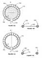
- a symmetry axisexists through the midline of the magnetic resonance sensor 110, defined through the centre of the isolation circuit 115 and the opposing point on the magnetic resonance sensor which is shown as line A-A in Figures 10A and 11A . Electrodes that are oppositely disposed to each other with reference to this line of symmetry are joined to each other by conducting wires or ribbons.
- Figures 10A and 10Bshow an embodiment, where wires 165 joining the oppositely opposed electrodes 168 run across the aperture 180 of the magnetic resonance sensor 110.
- Figures 11A and 11Bshow an alternative embodiment, where the electrodes 160 are linked sequentially by thin wires 170 along the edge of the sensor 110.
- the wire diametermust be small compared to the minor radius of the magnetic resonance sensor.
- a combination of wiresrun across the aperture and segments of wire joining consecutive electrodes to enable formation of an equipotential across the multi-electrode structure.
- the capacitance between each electrode and the magnetic resonance sensoris large compared to the capacitance between the electrode and the disturbing voltage source.
- the impedance of the wires joining the electrodesis small compared to the electrode-sensor capacitance.
- conductively joined electrodesessentially act as one single equipotential. Since electrodes are joined across the axis of symmetry, the electrodes act to provide a symmetrised voltage distribution across the magnetic resonance sensor. This symmetric voltage distribution is subsequently rejected by the isolation circuit and compensation circuit (in embodiments employing a compensation circuit).
- the multiple electrodescannot be replaced with one single floating electrode; it is important to maintain some discontinuity between electrodes.
- the electrodesare made of conducting material having thickness much less than the material electrical skin depth. This reduces the losses in the electrodes. It is also beneficial if the electrodes are shaped to conform to a surface parallel to the surface of the magnetic resonance sensor. That is, if the surface of the voltage distribution electrode is uniformly spaced from the surface of the magnetic resonance sensor. This reduces current proximity effects in the electrodes.
- the electrodesare advantageously combined with embodiments simultaneously employing the isolation circuit, and optionally with those also employing a compensation circuit. It will be appreciated that the isolation and compensation circuits do not require the electrode arrangement for useful operation.
Landscapes
- Physics & Mathematics (AREA)
- Condensed Matter Physics & Semiconductors (AREA)
- General Physics & Mathematics (AREA)
- Health & Medical Sciences (AREA)
- Epidemiology (AREA)
- Measuring Magnetic Variables (AREA)
- Magnetic Resonance Imaging Apparatus (AREA)
Description
- The present invention relates to an apparatus suitable for detecting Magnetic Resonance (MR) signals.
- MR sensors based on Faraday Law detection may couple to both electric and magnetic field components of Radio Frequency Interference (RFI). This RFI is known to emanate from both natural and man-made sources. Electric coupling can occur when common mode voltages on the sensor structure are generated through capacitive coupling to ambient electric fields (such as RF electric field voltages and gradients due to being in close proximity to human limbs). Magnetic coupling can occur when RFI magnetic fields thread the aperture of the sensor used for detection. These magnetic fields may originate from distant transmitters or close-in sources such as nearby mains wiring.
- In applications, such as medical imaging, electromagnetic shielding (such as an electrically conductive box or a shielded room) is used to prevent extraneous RFI from interfering with the MR signal. However, such techniques are not suitable in many potential applications of MR detection. For example, it is not practical to use electromagnetic shielding for bulk material such as mineral containing material being moved on a conveyor or if the MR detection device needs to be portable.
WO 2008/104895 describes apparatus for magnetic resonance excitation and detection at two measurement frequencies using planar coils. The coils are shielded by a ground plane.US 2009/251145 describes two inductively coupled coils, a first coil for transmitting and receiving a magnetic resonance signal and a second coil for changing a resonance frequency of the first coil. The second coil includes a switch that is used to switch between different resonance operating frequencies during magnetic resonance measurements.- An RF shield may be placed to the second coil on the other side of the first coil.
US 2005/059882 is intended for use in NMR imaging of human heads. A dome-shaped resonator is described with a similarly shaped dome-shaped shield that is in close proximity to the resonator.WO 2007 / 109426 describes various embodiments of loop resonators that have shields associated with them. The resonators and shields are part of an NMR imaging system. The shields have planar portions and angled wings which shield the loop resonators from each other.- The invention provides an apparatus as claimed in claim 1. Further features of the invention are apparent from the dependent claims 2-15.
- In an embodiment, the depth of the concavity of the shield member is at least 30% of the diameter of the magnetic resonance sensor.
- In an embodiment, the shield member is composed of a mesh.
- In an embodiment, the magnetic resonance sensor is a single turn loop or ribbon.
- In an embodiment, the magnetic resonance sensor is a multi-turn loop or ribbon.
- In an embodiment, the magnetic resonator is a single turn loop or ribbon.
- In an embodiment, the magnetic resonator is a multi turn loop or ribbon.
- In an embodiment of the apparatus according to
claim 11, the capacitor is connected halfway along the length of the primary winding of the isolation transformer. - In an embodiment of the apparatus according to
claim 11, the inverting circuit is a 1:1 impedance ratio transformer with counter-fed windings. - In an embodiment, the magnetic resonance sensor comprises an inductor and at least one capacitor.
- In an embodiment, there are an even number of capacitors arranged symmetrically relative to the inductor.
- In an embodiment, the inductor is a single turn inductive loop or ribbon.
- In an embodiment, the inductor is a multi-turn inductive coil.
- In an embodiment of the apparatus according to claim 12, the voltage distribution electrodes are linked by an electrical connector extending along an edge of the magnetic resonance sensor.
- In an embodiment of the apparatus according to claim 13, there are at least two pairs of voltage distribution electrodes and some of the electrodes are linked by electrical connectors extending between neighbouring electrodes.
Figure 1 is a perspective view of an apparatus for detecting magnetic resonance signals;Figure 2 is a cross-sectional view of the apparatus shown inFigure 1 ;Figure 3 is a cross-sectional view of an alternative apparatus for detecting magnetic resonance signals;Figure 4 is a block diagram of the apparatus for detecting magnetic resonance signals;Figure 5 is a circuit diagram of the apparatus shown inFigure 4 ;Figure 6 is a circuit diagram of the isolation circuit shown inFigure 5 ;Figure 7 is a circuit diagram of an alternative magnetic resonance sensor;Figure 8 shows a typical relationship of the apparatus relative to a target;Figure 9 show an example of a shield member with perforations;Figures 10A and 10B show a first example of a magnetic resonator incorporating a set of floating electrodes; andFigures 11A and 11B show a second example of a magnetic resonator incorporating a set of floating electrodes- Herein the term "magnetic resonance" (MR) refers to both Nuclear Magnetic Resonance (NMR) and Nuclear Quadrupole Resonance (NQR). NMR and NQR are methods having wide application in measurement and characterisation of materials. These methods are routinely used as a laboratory tool to investigate bonding and molecular structure. They have also found use in real-time detection and characterisation of minerals and other substances such as narcotics or explosives. There are many classes of NMR and NQR; for example, zero-field NMR in magnetically ordered materials, or double resonance NQR. For the purposes of the specification, all subclasses of NMR or NQR are included in the term "magnetic resonance".
- Referring to the drawings, there is shown an apparatus suitable for detecting magnetic resonance signals, comprising a magnetic resonance sensor arranged to respond to magnetic resonance signals. The apparatus has components for reducing the effects of magnetic coupling and optionally, also electric coupling on the magnetic resonance sensor.
- Herein, "magnetic coupling" refers to the situation where the unwanted output terminal voltage is driven predominantly by interfering magnetic fields. Herein, "electric coupling" refers to the additional case where the unwanted terminal voltage is also driven by interfering electric fields. Strictly speaking, for non-zero frequency disturbances the interfering magnetic and electric fields are in any case coupled through Maxwell's equations. However, the terms "electric coupling" and "magnetic coupling" still retain meaning in, for example, a quasi-static approximation to the interference problem.
- Electric coupling may occur, for instance, when common mode voltages on the sensor structure are generated through capacitive coupling to ambient electric fields. These voltages may result in sensor terminal voltages due to asymmetrical impedance distribution on each side of the sensor terminals. Alternatively, electric field gradients can contribute to terminal voltages, even in the case of symmetric impedance distribution at the terminal. The problem of electric coupling is especially severe in close proximity to human limbs, which may support significant RF electric field voltages and gradients.
- Magnetic coupling occurs when radiofrequency interference (RFI) magnetic fields thread the aperture of the inductor used for Faraday detection. These magnetic fields may originally emanate from distant transmitters located in the far field. In this case the inductor used for detection behaves as a small loop antenna receiver. Other close-in sources may also contribute to RFI magnetic fields, such as nearby mains wiring.
- In the embodiments of
Figures 1 to 11 , as in most MR measurements, radiofrequency (RF) electromagnetic near-fields from the MR sensor are employed to excite resonances in materials. That is, in the embodiment, as in many applications known in the art, the MR sensor may be used to both excite and detect MR signals. The configuration of sensors to provide both excitation of resonances in materials and detection of MR signals is known to persons skilled in the art. However, in the case where excitation of resonances in materials is provided by other apparatus, the embodiment may be used to detect MR signals only. - Depending on the application, the sensor RF near fields may be applied to materials either in the form of discrete pulses or as a continuous wave (CW) excitation. The response of the material may be regarded as a time varying magnetisation having an associated RF magnetic field. Thus, RF field excited due to sample magnetisation by the applied stimulus impinges on the near-field region of a sensor and voltages are developed at output terminals of the sensor. These terminal voltages are proportional to the time rate change of magnetic flux threading the sensor aperture, thus enabling magnetic resonance signals to be detected and processed.
Figure 1 is a schematic perspective view which illustrates the physical arrangement of theapparatus 100 for detecting magnetic resonance signals of the embodiment. The purpose of the physical arrangement shown inFigure 1 is to reduce interference due to magnetic coupling.Figure 8 , is a schematic plan view of the apparatus in one application where the target sample is material 320 on aconveyor 310, which shows theapparatus 100 facing the target sample as indicated generally by arrow A. Theapparatus 100 comprises amagnetic resonance sensor 110 adapted to respond to magnetic resonance signal, ashield member 130 electrically isolated from theMR sensor 110 and adapted to shield the magnetic resonance sensor from magnetic coupling, and amagnetic resonator 150 electrically isolated from theshield member 130 and themagnetic resonance sensor 110.- It will be appreciated that the elements of the
apparatus 100 set up a reference frame which enable attribution of mitigation of the effect of sources of magnetic coupling to particular components of the apparatus. That is, when themagnetic resonance sensor 110 faces the target, theshield member 130 is behind the magnetic resonance sensor to shield themagnetic resonance sensor 110 from magnetic coupling with sources other than magnetic resonance signal from the target. Magnetic coupling which is not, or cannot, be blocked by theshield member 130 is at least partially compensated for by themagnetic resonator 150 as described in further detail below. - In this embodiment, the
magnetic resonance sensor 110 is a circular single turn inductive loop having tuning elements andoutput circuitry 115. The tuning elements tune themagnetic resonance sensor 110 to about or close to a desired or predetermined magnetic resonance operating frequency when the displacement between themagnetic resonance sensor 110 and theshield member 130 is fixed in a given configuration. The tuningelements 115 also enable the desired excitation to be delivered. Such tuning elements are well understood in the art and accordingly are not described herein. The output allows a magnetic resonance signal voltage to be obtained. - Persons skilled in the art will appreciate that the
magnetic resonance sensor 110 need not be a circular single turn loop. For example, the shape of the magnetic resonance sensor can be different and/or can be a multi-turn loop or a ribbon etc. Persons skilled in the art will appreciate that a number of factors will influence the selection of the type and shape ofMR sensor 110, including the desired operating frequency of the MR sensor and/or the application of the MR sensor. For example at lower frequencies, a multi-turn loop is advantageous as it reduces the physical size of the required tuning capacitance. Similarly, if the device is to be a hand held device, a more elongate shape rather than a circle may be preferred such that the overall dimensions of the device are not unwieldy. - In
Figure 1 , theshield member 130 is a dished, circular conductive member. It is envisaged however that the shield member need not be circular but in alternative embodiments can be elliptical or rectangular to match or complement the shape of the MR sensor. Themagnetic resonator 150 is a circular single turn loop havingtuning elements 155, the tuningelements 155 being adapted to tune themagnetic resonator 150 to exhibit a resonance below the desired or predetermined magnetic resonance operating frequency when themagnetic resonator 150 is electrically isolated. As with the MR sensor, in other embodiments, themagnetic resonator 150 can also be multi-turn coil or a non-circular inductor. - In the
apparatus 100 ofFigure 1 , the diameter around the rim of theshield member 130 is in excess of the diameter of themagnetic resonance sensor 110. Persons skilled in the art will appreciate however that the diameter around the rim of theshield member 130 can also be approximately equal to themagnetic resonance sensor 110 if less "shielding" is required. In the apparatus ofFigure 1 , the diameter of themagnetic resonator 150 is approximately equal to the diameter around the rim of theshield member 130. Persons skilled in the art will appreciate however that the diameter of themagnetic resonator 150 may be in excess of the diameter around the rim of theshield member 130 to provide greater resonance compensation. - The
magnetic resonance sensor 110 is exposed so that one side of the inductive loop can face a target to detect magnetic resonance signals from the non-shielded side of the sensor. Theshield member 130 is positioned behind themagnetic resonance sensor 110 so that the convex side of theshield member 130 can shield themagnetic resonance sensor 110 from magnetically coupling with sources other than magnetic resonance signal from the target. Themagnetic resonator 150 is positioned behind theshield member 130 so that it can scatter magnetic field towards the target (and hence the MR sensor 110) to at least partially compensate for any magnetic coupling that may occur between sources other than the target and themagnetic resonance sensor 110. - Thus, in use, the
apparatus 100 is directed at atarget sample 320 so that one side of the magnetic resonance sensor faces thetarget 320 to detect magnetic resonance signals from the target. By directing the apparatus towards the target, themagnetic resonance sensor 110 responds to magnetic resonance from thetarget 320. Generally speaking, the response may be regarded as a time varying magnetisation having an associated RF magnetic field which impinges on a near-field region of themagnetic resonance sensor 110. The terminal voltage is proportional to the time rate change of magnetic flux threading the magnetic resonance sensor aperture. - A cross-sectional view of the
apparatus 100 is illustrated inFigure 2 which shows that theshield member 130 is dish-shaped. Theshield member 130 thus has a concave side and an opposing convex side. It is advantageous if the maximum depth of the concavity of the shield member is at least 30% of the diameter of the magnetic resonance sensor. The concavity provided by the dished shield member is advantageous in that it reduces the potential for eddy currents to be developed in the shield member during transmission and reception of signals, thereby maintaining transmission efficiency (flux per unit available power) of the MR sensor and the receive efficiency (delivered power at sensor terminals for a given flux generated by the target sample). - In this embodiment, the
magnetic resonance sensor 110, theshield member 130 and themagnetic resonator 150 are arranged in a symmetric "stacked" arrangement so as to provide a high degree of suppression for magnetic coupling by interfering fields. The conductivity and thickness of the shield member is such that it significantly rejects incident magnetic field from penetrating through the wall of the shield member. In this respect, it will be appreciated that the shield member reduces the effect of interfering fields but does not (and does not need to) completely suppress their effect. - The
magnetic resonance sensor 110 is positioned in a manner such that there is a gap between themagnetic resonance sensor 110 andshield member 130 so that the two are electrically isolated from one another. In an embodiment, this gap can be created by a non-conductive material such as Perspex sheet(s). Persons skilled in the art will appreciate however that any suitable non-conductive separator can be used to electrically separate themagnetic resonance sensor 110 andshield member 130 and that the separator may take the form of flat sheets or stand-offs such as a series of leg members between theMR sensor 110 and theshield member 130. Themagnetic resonator 150 is similarly positioned in a manner such that there is also a gap between themagnetic resonator 150 and theshield member 130 so that the two are electrically isolated from one another again by a suitable non-conductive material. In practice, the displacement between themagnetic resonator 150 and theshield member 130 is be determined by trial and error by moving the magnetic resonator towards or away from the shield member (in a controlled environment when the apparatus is otherwise not operating) and determining a point where the resonance of the magnetic resonator "nulls" any unwanted magnetic coupling - i.e. by determining what displacement minimises unwanted magnetic coupling not blocked by theshield member 130. Once the displacement is determined, the magnetic resonator is fixed at this distance - e.g. with stand-offs. It will be appreciated that once the distance has been determined for a particular set of components and operating frequency it can be replicated. An alternative method of fixing the magnetic resonator position is to set the magnetic resonator at a position that provides an approximate null through a trial and error process. The tuning of the magnetic resonator may then be trimmed in the determined position to obtain an improved null. - Persons skilled in the art will appreciate that the concavity of the
shield member 130 and the displacement between themagnetic resonance sensor 110 andshield member 130 can be varied according to a variety of factors including the desired amount of sensitivity of themagnetic resonance sensor 110, the quality of magnetic resonance response sensed by themagnetic resonance sensor 110 and the desired amount of shielding required against magnetic coupling between themagnetic resonance sensor 110 etc. Persons skilled in the art will appreciate that the displacement between themagnetic resonator 150 and theshield member 130 is also dependent on a number of factors including the amount of resonance compensation required. It is envisaged that the displacement of the rim of the shield member to the magnetic resonance sensor may be varied according to desired characteristics of the RFI coupling suppression. - A cross-sectional view of one such alternative apparatus for detecting magnetic resonance signals 101 is illustrated in
Figure 3 . The apparatus also comprises amagnetic resonance sensor 111, ashield member 131 and amagnetic resonator 151. - In this embodiment, the
shield member 131 is also dish-shaped but the concavity of theshield member 131 is much greater than the embodiment shown inFigure 2 . - In this embodiment, the diameter of the
magnetic resonance sensor 111 is smaller than the diameter of the rim of theshield member 131. Themagnetic resonance sensor 111 is positioned relative to theshield member 131 such that theshield member 131 encompasses themagnetic resonance sensor 111. - As shown in
Figure 3 , the diameter of themagnetic resonator 151 is in excess of the diameter of the rim of theshield member 131. Themagnetic resonator 151 is positioned relative to theshield member 131 such that themagnetic resonator 151 encircles theshield member 131. - Accordingly, it will be appreciated that the
apparatus - Persons skilled in the art will appreciate that the specific construction of the apparatus will vary from implementation to implementation. In an example apparatus suited to scanning small items, the magnetic resonance sensor can be formed from a single loop having a diameter of 108mm, the shield member can be bowl shaped and have a diameter of 136mm and the magnetic resonator can be a ribbon having a diameter of 160mm. The elements are arranged such that the total stacked height is 59mm.
Figure 4 is a block diagram illustrating the circuit components of the embodiment of the apparatus which shows the components which are used to reduce electric coupling.Figure 4 does not show theshield member 130 or the magnetic resonator as these are not electrically coupled to theMR sensor 110.- In the block diagram of
Figure 4 , the circuit equivalent of the physicalmagnetic sensor 110 is the magneticresonance sensor circuit 210. Accordingly, theapparatus 100 comprises a magneticresonance sensor circuit 210 adapted to respond to magnetic resonance signals, anoutput 250, anisolation circuit 230 arranged between the magneticresonance sensor circuit 210 and theoutput 250 to transfer electrical energy from the magneticresonance sensor circuit 210 to theoutput 250 while reducing electrical energy electrically coupled to the magneticresonance sensor circuit 210 from transferring to theoutput 250, and acompensation circuit 280 connected to theisolation circuit 230 and theoutput 250 to compensate for electrical energy due to electric coupling within theisolation circuit 230. - An exemplary circuit diagram of the
apparatus 100 is illustrated inFigure 5 . A detailed view of theisolation circuit 230 of theapparatus 100 is shown inFigure 6 . - As shown in
Figure 5 , the magneticresonance sensor circuit 210 comprises aninductive coil 214 connected to a matching network for tunning the coil. In another example, the inductive coil may also be a single turn circular loop having high symmetry. In this embodiment, the matching network comprises acapacitor 218. Persons skilled in the art will appreciate that the matching network may comprise different elements depending on the desired operating characteristics such as the desired magnetic resonance operating frequency. Regardless of the number of elements in the matching network, it is advantageous if the elements are approximately balanced between each side of the inductive coil 214 - i.e. highly symmetrical. - In
Figure 5 , theisolation circuit 230 is an isolation transformer. A detailed view of theisolation circuit 230 is provided inFigure 6 which shows that the primary winding 234 of the isolation transformer is connected to thematching network 218. The secondary winding 238 of the isolation transformer is connected to theoutput 250 and referenced to ground. Persons skilled in the art will appreciate that the secondary winding may be referenced to any system voltage and that the isolation transformer may also serve the purpose of impedance matching transformation. - In this embodiment, the isolation transformer acts to electrically "float" the active elements of the magnetic resonance sensor circuit 210 (that is, the
inductive coil 214 and the matching network 218). The primary winding 234 of the transformer floats with these elements. - In this way, the magnetic
resonance sensor circuit 210 and primary winding 234 can rise to a voltage that can prevent current flow between the magneticresonance sensor circuit 210 and external voltage sources. Thus, even if the magneticresonance sensor circuit 210 has a significant common mode voltage (which may be generated on the MR sensor through capacitive coupling to ambient electric fields), the isolation imparted by the isolation transformer reduces the amount of this voltage (or prevents portion of this voltage) from appearing at theoutput 250. - The
compensation circuit 280 illustrated inFigure 5 comprises acapacitor 288 and avoltage inverting circuit 284 connected to the capacitor. In this embodiment, thecapacitor 288 is connected via ahalfway tap 236 connected halfway along the length of the primary winding 234 of theisolation transformer 230. (In practical terms, this capacitor may not tap the primary winding 234 of the isolation transformer at a point exactly halfway along its length while still acting adequately to provide compensation.) Persons skilled in the art will appreciate that the capacitance value of thecapacitor 288 can be set to minimize any voltage due to electric coupling at the output. In the apparatus ofFigure 5 , thevoltage inverting circuit 284 is a 1:1 impedance ratio transformer with counter-fed windings which is connected directly to the output. Persons skilled in the art will appreciate that other voltage inverting devices can be used for example, an amplifier circuit. - The
compensation circuit 280 compensates for imperfect isolation between the primary and secondary windings 234,238 of the isolation transformer because of interwinding capacitance. Specifically, thecompensation circuit 280 compensates for imperfect isolation by reducing common mode currents transmitted through the transformer. In this embodiment, if the current through thecapacitor 288 connected to thehalfway tap 236 has similar magnitude to that in the interwinding capacitance, then cancellation of additional unwanted common mode voltage at the output can occur. It is envisaged that other compensation or "neutralisation" techniques can also be used to similarly limit the effect of common mode current on the output. Further it will be appreciated that some advantage is obtained by using the isolation circuit without the compensation circuit. Figure 7 is a circuit diagram of an alternativeMR resonance sensor 211. TheMR resonance sensor 211 comprises aninductive coil 215 andcapacitors inductive coil 215. In this embodiment, theinductive coil 215 is a multi-turn coil. However, it is envisaged that a circular single turn loop or any design having high symmetry and low impedance to allow for a simple tuning design and low sensitivity to field gradients can also be used.- One or more embodiments of the present application can be used in a wide variety of applications. For example, an embodiment can be used to detect specific minerals in bulk material in open plant environments (such as conveyors, slurry systems, boreholes or rock faces), detect narcotics and explosives carried on humans or in parcels in real-time, and measure and characterize materials in laboratories to investigate bonding and molecular structure.
- In some embodiments, it is advantageous that the shield member has some perforations to increase the magnetic coupling between the magnetic resonance sensor and the magnetic resonator. The control of the coupling by this mechanism allows variation in the spacing between elements of the apparatus, leading to improved sensitivity with judicious spacing of elements. The perforations may take the form of circular holes or holes of other shape to allow additional magnetic flux to thread both the magnetic resonance sensor and magnetic resonator, thereby modifying the coupling between these elements. The spacing of holes may be arranged regularly in the form of a mesh. The holes may also be arranged in an array.
Figure 9 shows an example of embodiment where theshield member 900 containsperforations 910. Depending on the embodiment, the perforations may cover up to 50% of the surface area. - In other embodiments, a sieve type mesh is possible, but meshes may be employed where the conducting elements are flattened and present a larger area than what is normally associated with a sieve. In other embodiments, the mesh may be formed of conducting elements carried by a supporting material, such as by being woven into a fabric. In practice a bonded-type mesh (where metal crossovers have physical bonding rather than just touching) is the most advantageous.
- In other embodiments, the above apparatus is modified to provide for the mitigation of the effects of asymmetrically applied voltages across the magnetic resonance sensor. Asymmetric voltages may occur, for example, when positioning one side of the sensor in closer proximity to a voltage disturbance than the other side of the sensor. The asymmetric voltage distribution may drive unequal currents through the isolation circuit, giving rise to an apparent magnetic resonance signal. To counteract this effect multiple floating electrodes (i.e., electrodes that make no physical contact with either the magnetic resonance sensor, shield member or magnetic resonator) are placed near the magnetic resonance sensor at close proximity to enable formation of an equipotential. Due to the incorporation of an isolation circuit, a symmetry axis exists through the midline of the
magnetic resonance sensor 110, defined through the centre of theisolation circuit 115 and the opposing point on the magnetic resonance sensor which is shown as line A-A inFigures 10A and 11A . Electrodes that are oppositely disposed to each other with reference to this line of symmetry are joined to each other by conducting wires or ribbons. Figures 10A and 10B show an embodiment, wherewires 165 joining the oppositely opposed electrodes 168 run across theaperture 180 of themagnetic resonance sensor 110.Figures 11A and 11B show an alternative embodiment, where theelectrodes 160 are linked sequentially bythin wires 170 along the edge of thesensor 110. In this instance, the wire diameter must be small compared to the minor radius of the magnetic resonance sensor.- In another embodiment, a combination of wires run across the aperture and segments of wire joining consecutive electrodes to enable formation of an equipotential across the multi-electrode structure.
- In such arrangements, the capacitance between each electrode and the magnetic resonance sensor is large compared to the capacitance between the electrode and the disturbing voltage source. The impedance of the wires joining the electrodes is small compared to the electrode-sensor capacitance. Under these circumstances conductively joined electrodes essentially act as one single equipotential. Since electrodes are joined across the axis of symmetry, the electrodes act to provide a symmetrised voltage distribution across the magnetic resonance sensor. This symmetric voltage distribution is subsequently rejected by the isolation circuit and compensation circuit (in embodiments employing a compensation circuit). The multiple electrodes cannot be replaced with one single floating electrode; it is important to maintain some discontinuity between electrodes.
- It is advantageous if the electrodes are made of conducting material having thickness much less than the material electrical skin depth. This reduces the losses in the electrodes. It is also beneficial if the electrodes are shaped to conform to a surface parallel to the surface of the magnetic resonance sensor. That is, if the surface of the voltage distribution electrode is uniformly spaced from the surface of the magnetic resonance sensor. This reduces current proximity effects in the electrodes.
- The electrodes are advantageously combined with embodiments simultaneously employing the isolation circuit, and optionally with those also employing a compensation circuit. It will be appreciated that the isolation and compensation circuits do not require the electrode arrangement for useful operation.
- Persons skilled in the art will appreciate that a number of variations can be made to the above embodiments.
- In the claims which follow and in the preceding description of the invention, except where the context requires otherwise due to express language or necessary implication, the word "comprise" or variations such as "comprises" or "comprising" is used in an inclusive sense, i.e. to specify the presence of the stated features but not to preclude the presence or addition of further features in various embodiments of the invention.
Claims (15)
- An apparatus for detecting magnetic resonance signals from a target, comprising:a magnetic resonance sensor for near-field Faraday detection of magnetic resonance signals from a target by responding to the magnetic resonance signals to output a magnetic resonance signal voltage;a conductive shield member electrically isolated from the magnetic resonance sensor, the shield member being dish-shaped so as to define a concave side and an opposing convex side and positioned relative to the magnetic resonance sensor with the magnetic resonance sensor on the concave side of the shield member such that when the magnetic resonance sensor faces the target, the shield member is behind the magnetic resonance sensor to at least partially shield the magnetic resonance sensor from magnetically coupling with sources of interfering magnetic fields other than the magnetic resonance signals; anda magnetic resonator positioned on the convex side of the shield member, the magnetic resonator electrically isolated from the shield member and the magnetic resonance sensor, the magnetic resonator being arranged to resonate and scatter magnetic field towards the target, and hence the magnetic resonance sensor, to at least partially compensate for the magnetic coupling of sources of interfering magnetic fields other than the target with the magnetic resonance sensor.
- An apparatus as claimed in claim 1, wherein the magnetic resonance sensor is encompassed within the shield member by being located within the concavity of the concave side of the shield member.
- An apparatus as claimed in claim 1 or claim 2, wherein the shield member is encircled by the magnetic resonator by the magnetic resonator having a larger diameter than the shield member.
- An apparatus as claimed in any one of claims 1 to 3, wherein
the magnetic resonance sensor comprises a first tuning element for tuning the magnetic resonance sensor to operate at about a predetermined operating frequency; and
the magnetic resonator comprises a second tuning element for tuning the magnetic resonator to a resonance below the predetermined operating frequency. - An apparatus as claimed in any one of claims 1 to 4, wherein the magnetic resonance sensor and the magnetic resonator are circular.
- An apparatus as claimed in any one of claims 1 to 5, wherein the shield member comprises a plurality of perforations.
- An apparatus as claimed in any one of claims 1 to 6, comprising:an output for outputting the magnetic resonance signal voltage; andan isolation circuit arranged between the magnetic resonance sensor and the output to transfer electrical energy from the magnetic resonance sensors response to the magnetic resonance signals to the output while reducing electrical energy electrically coupled to the magnetic resonance sensor by interfering electrical fields from transferring to the output.
- An apparatus as claimed in claim 7, further comprising a compensation circuit connected to the isolation circuit and the output to compensate for electrical energy due to electric coupling by interfering electrical fields within the isolation circuit.
- An apparatus as claimed in claim 7 or claim 8, wherein the isolation circuit is an isolation transformer.
- An apparatus as claimed in claim 9, wherein the isolation transformer comprises:a primary winding connected to the magnetic resonance sensor; anda secondary winding connected to the output, the secondary winding being referenced to a system voltage.
- An apparatus as claimed in claim 10, wherein the compensation circuit comprises:a capacitor connected to the primary winding of the isolation transformer; anda voltage inverting circuit connected to the capacitor.
- An apparatus as claimed in any one of claims 9 to 11, comprising at least one pair of voltage distribution electrodes in proximity to, but electrically isolated from, the magnetic resonance sensor, each pair of voltage distribution electrodes being arranged symmetrically relative to a line of symmetry defined by a midline of the magnetic resonance sensor which extends through the isolation circuit, the voltage distribution electrodes being electrically connected to enable formation of an equipotential.
- An apparatus as claimed in claim 12, wherein at least one pair of voltage distribution electrodes is connected by an electrical connector extending across an aperture of the magnetic resonance sensor.
- An apparatus as claimed in claim 12, wherein a thickness of each voltage distribution electrode is less than the electrical skin depth of a material from which each voltage distribution electrode is formed.
- An apparatus as claimed in claim 12, wherein the surface of each voltage distribution electrode is uniformly spaced from the magnetic resonance sensor.
Applications Claiming Priority (2)
| Application Number | Priority Date | Filing Date | Title |
|---|---|---|---|
| AU2009905897AAU2009905897A0 (en) | 2009-12-02 | An apparatus for detecting signals | |
| PCT/AU2010/001600WO2011066600A1 (en) | 2009-12-02 | 2010-11-29 | An apparatus for detecting signals |
Publications (3)
| Publication Number | Publication Date |
|---|---|
| EP2510372A1 EP2510372A1 (en) | 2012-10-17 |
| EP2510372A4 EP2510372A4 (en) | 2013-05-22 |
| EP2510372B1true EP2510372B1 (en) | 2015-07-01 |
Family
ID=44114544
Family Applications (1)
| Application Number | Title | Priority Date | Filing Date |
|---|---|---|---|
| EP10834080.3AActiveEP2510372B1 (en) | 2009-12-02 | 2010-11-29 | An apparatus for detecting magnetic resonance signals |
Country Status (7)
| Country | Link |
|---|---|
| US (1) | US9335390B2 (en) |
| EP (1) | EP2510372B1 (en) |
| CN (1) | CN102713655B (en) |
| AU (1) | AU2010327357B2 (en) |
| CL (1) | CL2012001448A1 (en) |
| WO (1) | WO2011066600A1 (en) |
| ZA (1) | ZA201203657B (en) |
Families Citing this family (7)
| Publication number | Priority date | Publication date | Assignee | Title |
|---|---|---|---|---|
| CN104266665B (en)* | 2014-09-17 | 2016-09-28 | 上海兰宝传感科技股份有限公司 | Inductance type transducer |
| WO2017031535A1 (en)* | 2015-08-24 | 2017-03-02 | Commonwealth Scientific And Industrial Research Organisation | An apparatus for on-line detection of magnetic resonance signals from a target material in a mineral slurry |
| US10416248B2 (en)* | 2015-08-24 | 2019-09-17 | Commonwealth Scientific And Industrial Research Organisation | On-line magnetic resonance measurement of conveyed material |
| US11307055B2 (en) | 2019-09-18 | 2022-04-19 | Analog Devices International Unlimited Company | Sensor with magnetic shield |
| WO2021127735A1 (en)* | 2019-12-24 | 2021-07-01 | Commonwealth Scientific And Industrial Research Organisation | An apparatus for the measurement of ore in mine ore benches |
| WO2021127734A1 (en)* | 2019-12-24 | 2021-07-01 | Commonwealth Scientific And Industrial Research Organisation | An apparatus for the measurement of ore in mine haul vehicles |
| KR102623195B1 (en)* | 2021-11-26 | 2024-01-10 | 대한전선 주식회사 | Shield ring included in the spacer having electronic transformer for gas insulated switchgear |
Family Cites Families (25)
| Publication number | Priority date | Publication date | Assignee | Title |
|---|---|---|---|---|
| US5594342A (en)* | 1992-06-01 | 1997-01-14 | Conductus, Inc. | Nuclear magnetic resonance probe coil with enhanced current-carrying capability |
| DE4301557C2 (en) | 1993-01-21 | 1995-07-06 | Siemens Ag | Antenna arrangement with shielding for a magnetic resonance imaging device |
| GB9307646D0 (en) | 1993-04-14 | 1993-06-02 | Marconi Gec Ltd | Electric field screen |
| US6028429A (en)* | 1996-07-17 | 2000-02-22 | Fonar Corporation | Composite MRI antenna with reduced stray capacitance |
| DE19810837C2 (en)* | 1998-03-12 | 2002-12-12 | Siemens Ag | High frequency antenna for a magnetic resonance device |
| US6249121B1 (en)* | 1999-05-17 | 2001-06-19 | General Electric Company | RF body coil |
| US6498487B1 (en)* | 2000-01-25 | 2002-12-24 | Varian, Inc. | Distributed capacitance inserts for NMR probes |
| US6888153B2 (en)* | 2000-04-05 | 2005-05-03 | University Of Washington | Capacitive shield for containing radiofrequency magnetic fields |
| US6538442B2 (en)* | 2000-12-22 | 2003-03-25 | Ge Medical Systems Global Technology Company | MRI system having RF shielding gradient coil structure |
| US6885192B2 (en)* | 2002-02-06 | 2005-04-26 | The Regents Of The University Of California | SQUID detected NMR and MRI at ultralow fields |
| US6885194B2 (en) | 2002-05-03 | 2005-04-26 | Ge Medical Systems Global Technology Company, Llc | Method and apparatus for minimizing gradient coil and rf coil coupling |
| US7180950B2 (en) | 2002-11-01 | 2007-02-20 | Avago Technologies Fiber Ip (Singapore) Pte. Ltd. | Low-noise feedback cancellation filter for enhanced common-mode rejection and noise immunity |
| US6927575B2 (en)* | 2003-01-21 | 2005-08-09 | General Electric Company | Surface coil decoupling means for MRI systems |
| US7250764B2 (en)* | 2003-09-12 | 2007-07-31 | Ge Medical Systems Global Technology Company, Llc | Shielded dome resonator for MR scanning of a cerebrum |
| AR048373A1 (en) | 2004-07-08 | 2006-04-26 | Spinlock Srl | A DEVICE AND A METHOD FOR MEASURING DIRECTLY AND IN REAL TIME, THE PROPORTION AND FLOW OF THE DIFFERENT COMPONENTS THAT CONFORM A MULTICOMPONENT COMPLEX FLUID, A PRODUCTION LINE PROVISION FOR A MULTICOMPONENT COMPLEX FLUID THAT USES A SAID AND DEPOSITIVE METHOD |
| US20060084861A1 (en)* | 2004-10-18 | 2006-04-20 | Topspin Medical (Isreal) Ltd. | Magnet and coil configurations for MRI probes |
| US7501825B2 (en)* | 2005-03-02 | 2009-03-10 | New York University | Magnetic resonance imaging method and system |
| US20070096731A1 (en)* | 2005-11-03 | 2007-05-03 | Rf Sensors, Llc | Open-Shape Noise-Resilient Multi-Frequency Sensors |
| CN101405612B (en)* | 2006-03-22 | 2011-11-23 | 皇家飞利浦电子股份有限公司 | Shielded multix coil array for parallel high field MRI |
| EP2005218A4 (en) | 2006-04-07 | 2012-03-07 | Us Gov Health & Human Serv | INDUCTIVE DECOUPLING OF AN RF COIL NETWORK |
| US7327137B1 (en)* | 2006-11-14 | 2008-02-05 | Ge Homeland Protection, Inc. | Apparatus and method for non-symmetric magnetic field balancing in an inspection scanner |
| CN101790693B (en)* | 2007-02-26 | 2013-12-11 | 皇家飞利浦电子股份有限公司 | Doubly resonant high field radio frequency surface coils for magnetic resonance |
| US7743860B2 (en) | 2007-10-09 | 2010-06-29 | Ford Global Technologies, Llc | Holding a hybrid electric vehicle on an inclined surface |
| JP5247214B2 (en)* | 2008-04-04 | 2013-07-24 | 株式会社日立製作所 | High frequency magnetic field coil and magnetic resonance imaging apparatus |
| US20100073000A1 (en) | 2008-09-22 | 2010-03-25 | Insight Neuroimaging Systems, Llc | Radio frequency coil apparatus and methods |
- 2010
- 2010-11-29EPEP10834080.3Apatent/EP2510372B1/enactiveActive
- 2010-11-29CNCN201080061826.9Apatent/CN102713655B/enactiveActive
- 2010-11-29USUS13/513,443patent/US9335390B2/enactiveActive
- 2010-11-29AUAU2010327357Apatent/AU2010327357B2/enactiveActive
- 2010-11-29WOPCT/AU2010/001600patent/WO2011066600A1/enactiveApplication Filing
- 2012
- 2012-05-18ZAZA2012/03657Apatent/ZA201203657B/enunknown
- 2012-06-01CLCL2012001448Apatent/CL2012001448A1/enunknown
Also Published As
| Publication number | Publication date |
|---|---|
| EP2510372A1 (en) | 2012-10-17 |
| US20120242340A1 (en) | 2012-09-27 |
| WO2011066600A1 (en) | 2011-06-09 |
| US9335390B2 (en) | 2016-05-10 |
| AU2010327357A1 (en) | 2012-06-21 |
| ZA201203657B (en) | 2013-08-28 |
| CN102713655A (en) | 2012-10-03 |
| AU2010327357B2 (en) | 2014-09-18 |
| EP2510372A4 (en) | 2013-05-22 |
| CN102713655B (en) | 2016-01-20 |
| CL2012001448A1 (en) | 2013-04-12 |
Similar Documents
| Publication | Publication Date | Title |
|---|---|---|
| EP2510372B1 (en) | An apparatus for detecting magnetic resonance signals | |
| US4725779A (en) | NMR local coil with improved decoupling | |
| EP3685198B1 (en) | Device and method for foreign object detection in wireless energy transfer | |
| EP2097763B1 (en) | Rf coil for use in an mr imaging system, in combination with a metamaterial | |
| EP0047065B1 (en) | Distributed phase rf coil | |
| US20050146331A1 (en) | Transmit-receive coil system for nuclear quadrupole resonance signal detection in substances and components thereof | |
| GB2063569A (en) | Shielded balanced loop antennas | |
| US10191128B2 (en) | Device and method for loops-over-loops MRI coils | |
| EP0162534B1 (en) | Coil arrangements | |
| AU2016312967B2 (en) | On-line magnetic resonance measurement of conveyed material | |
| BR102017010197B1 (en) | METAL DETECTION DEVICE | |
| US20030016109A1 (en) | MR apparatus provided with an open magnet system and a quadrature coil system | |
| US11280861B2 (en) | Sheath wave barrier for magnetic resonance (MR) applications | |
| US20170045593A1 (en) | Device and Method for Electrically Linking Electronic Assemblies by Means of Symmetrical Shielded Cables | |
| US20170219667A1 (en) | Planar Standing Wave Trap for a Magnetic Resonance Tomograph | |
| US11460599B2 (en) | Shielded-loop-resonator based gradiometer probe | |
| GB2277160A (en) | Electric field screening arrangement for MRI RF coil | |
| EP0502585B1 (en) | Antenna device for a shoplifting detection system | |
| Kalagher | An Experimental Study for Determining Optimum Antenna Placement Within a Metallic Enclosure | |
| WO2025172774A1 (en) | Active antenna comprising a single-turn loop aerial |
Legal Events
| Date | Code | Title | Description |
|---|---|---|---|
| PUAI | Public reference made under article 153(3) epc to a published international application that has entered the european phase | Free format text:ORIGINAL CODE: 0009012 | |
| 17P | Request for examination filed | Effective date:20120620 | |
| AK | Designated contracting states | Kind code of ref document:A1 Designated state(s):AL AT BE BG CH CY CZ DE DK EE ES FI FR GB GR HR HU IE IS IT LI LT LU LV MC MK MT NL NO PL PT RO RS SE SI SK SM TR | |
| DAX | Request for extension of the european patent (deleted) | ||
| A4 | Supplementary search report drawn up and despatched | Effective date:20130419 | |
| RIC1 | Information provided on ipc code assigned before grant | Ipc:G01R 33/34 20060101AFI20130415BHEP Ipc:G01R 33/36 20060101ALI20130415BHEP Ipc:G01R 33/422 20060101ALI20130415BHEP | |
| GRAP | Despatch of communication of intention to grant a patent | Free format text:ORIGINAL CODE: EPIDOSNIGR1 | |
| INTG | Intention to grant announced | Effective date:20150217 | |
| GRAS | Grant fee paid | Free format text:ORIGINAL CODE: EPIDOSNIGR3 | |
| GRAA | (expected) grant | Free format text:ORIGINAL CODE: 0009210 | |
| AK | Designated contracting states | Kind code of ref document:B1 Designated state(s):AL AT BE BG CH CY CZ DE DK EE ES FI FR GB GR HR HU IE IS IT LI LT LU LV MC MK MT NL NO PL PT RO RS SE SI SK SM TR | |
| REG | Reference to a national code | Ref country code:GB Ref legal event code:FG4D | |
| REG | Reference to a national code | Ref country code:AT Ref legal event code:REF Ref document number:734281 Country of ref document:AT Kind code of ref document:T Effective date:20150715 Ref country code:CH Ref legal event code:EP | |
| REG | Reference to a national code | Ref country code:IE Ref legal event code:FG4D | |
| REG | Reference to a national code | Ref country code:DE Ref legal event code:R096 Ref document number:602010025638 Country of ref document:DE | |
| REG | Reference to a national code | Ref country code:SE Ref legal event code:TRGR | |
| REG | Reference to a national code | Ref country code:AT Ref legal event code:MK05 Ref document number:734281 Country of ref document:AT Kind code of ref document:T Effective date:20150701 | |
| REG | Reference to a national code | Ref country code:NL Ref legal event code:MP Effective date:20150701 | |
| REG | Reference to a national code | Ref country code:LT Ref legal event code:MG4D | |
| PG25 | Lapsed in a contracting state [announced via postgrant information from national office to epo] | Ref country code:LT Free format text:LAPSE BECAUSE OF FAILURE TO SUBMIT A TRANSLATION OF THE DESCRIPTION OR TO PAY THE FEE WITHIN THE PRESCRIBED TIME-LIMIT Effective date:20150701 Ref country code:LV Free format text:LAPSE BECAUSE OF FAILURE TO SUBMIT A TRANSLATION OF THE DESCRIPTION OR TO PAY THE FEE WITHIN THE PRESCRIBED TIME-LIMIT Effective date:20150701 Ref country code:NO Free format text:LAPSE BECAUSE OF FAILURE TO SUBMIT A TRANSLATION OF THE DESCRIPTION OR TO PAY THE FEE WITHIN THE PRESCRIBED TIME-LIMIT Effective date:20151001 Ref country code:GR Free format text:LAPSE BECAUSE OF FAILURE TO SUBMIT A TRANSLATION OF THE DESCRIPTION OR TO PAY THE FEE WITHIN THE PRESCRIBED TIME-LIMIT Effective date:20151002 | |
| PG25 | Lapsed in a contracting state [announced via postgrant information from national office to epo] | Ref country code:ES Free format text:LAPSE BECAUSE OF FAILURE TO SUBMIT A TRANSLATION OF THE DESCRIPTION OR TO PAY THE FEE WITHIN THE PRESCRIBED TIME-LIMIT Effective date:20150701 Ref country code:RS Free format text:LAPSE BECAUSE OF FAILURE TO SUBMIT A TRANSLATION OF THE DESCRIPTION OR TO PAY THE FEE WITHIN THE PRESCRIBED TIME-LIMIT Effective date:20150701 Ref country code:IS Free format text:LAPSE BECAUSE OF FAILURE TO SUBMIT A TRANSLATION OF THE DESCRIPTION OR TO PAY THE FEE WITHIN THE PRESCRIBED TIME-LIMIT Effective date:20151101 Ref country code:PT Free format text:LAPSE BECAUSE OF FAILURE TO SUBMIT A TRANSLATION OF THE DESCRIPTION OR TO PAY THE FEE WITHIN THE PRESCRIBED TIME-LIMIT Effective date:20151102 Ref country code:HR Free format text:LAPSE BECAUSE OF FAILURE TO SUBMIT A TRANSLATION OF THE DESCRIPTION OR TO PAY THE FEE WITHIN THE PRESCRIBED TIME-LIMIT Effective date:20150701 Ref country code:AT Free format text:LAPSE BECAUSE OF FAILURE TO SUBMIT A TRANSLATION OF THE DESCRIPTION OR TO PAY THE FEE WITHIN THE PRESCRIBED TIME-LIMIT Effective date:20150701 Ref country code:PL Free format text:LAPSE BECAUSE OF FAILURE TO SUBMIT A TRANSLATION OF THE DESCRIPTION OR TO PAY THE FEE WITHIN THE PRESCRIBED TIME-LIMIT Effective date:20150701 | |
| REG | Reference to a national code | Ref country code:DE Ref legal event code:R097 Ref document number:602010025638 Country of ref document:DE | |
| PG25 | Lapsed in a contracting state [announced via postgrant information from national office to epo] | Ref country code:IT Free format text:LAPSE BECAUSE OF FAILURE TO SUBMIT A TRANSLATION OF THE DESCRIPTION OR TO PAY THE FEE WITHIN THE PRESCRIBED TIME-LIMIT Effective date:20150701 Ref country code:SK Free format text:LAPSE BECAUSE OF FAILURE TO SUBMIT A TRANSLATION OF THE DESCRIPTION OR TO PAY THE FEE WITHIN THE PRESCRIBED TIME-LIMIT Effective date:20150701 Ref country code:EE Free format text:LAPSE BECAUSE OF FAILURE TO SUBMIT A TRANSLATION OF THE DESCRIPTION OR TO PAY THE FEE WITHIN THE PRESCRIBED TIME-LIMIT Effective date:20150701 Ref country code:CZ Free format text:LAPSE BECAUSE OF FAILURE TO SUBMIT A TRANSLATION OF THE DESCRIPTION OR TO PAY THE FEE WITHIN THE PRESCRIBED TIME-LIMIT Effective date:20150701 Ref country code:DK Free format text:LAPSE BECAUSE OF FAILURE TO SUBMIT A TRANSLATION OF THE DESCRIPTION OR TO PAY THE FEE WITHIN THE PRESCRIBED TIME-LIMIT Effective date:20150701 | |
| PLBE | No opposition filed within time limit | Free format text:ORIGINAL CODE: 0009261 | |
| STAA | Information on the status of an ep patent application or granted ep patent | Free format text:STATUS: NO OPPOSITION FILED WITHIN TIME LIMIT | |
| PG25 | Lapsed in a contracting state [announced via postgrant information from national office to epo] | Ref country code:RO Free format text:LAPSE BECAUSE OF FAILURE TO SUBMIT A TRANSLATION OF THE DESCRIPTION OR TO PAY THE FEE WITHIN THE PRESCRIBED TIME-LIMIT Effective date:20150701 | |
| 26N | No opposition filed | Effective date:20160404 | |
| PG25 | Lapsed in a contracting state [announced via postgrant information from national office to epo] | Ref country code:LU Free format text:LAPSE BECAUSE OF FAILURE TO SUBMIT A TRANSLATION OF THE DESCRIPTION OR TO PAY THE FEE WITHIN THE PRESCRIBED TIME-LIMIT Effective date:20151129 Ref country code:MC Free format text:LAPSE BECAUSE OF FAILURE TO SUBMIT A TRANSLATION OF THE DESCRIPTION OR TO PAY THE FEE WITHIN THE PRESCRIBED TIME-LIMIT Effective date:20150701 | |
| REG | Reference to a national code | Ref country code:CH Ref legal event code:PL | |
| PG25 | Lapsed in a contracting state [announced via postgrant information from national office to epo] | Ref country code:LI Free format text:LAPSE BECAUSE OF NON-PAYMENT OF DUE FEES Effective date:20151130 Ref country code:CH Free format text:LAPSE BECAUSE OF NON-PAYMENT OF DUE FEES Effective date:20151130 | |
| REG | Reference to a national code | Ref country code:IE Ref legal event code:MM4A | |
| REG | Reference to a national code | Ref country code:FR Ref legal event code:ST Effective date:20160729 | |
| PG25 | Lapsed in a contracting state [announced via postgrant information from national office to epo] | Ref country code:SI Free format text:LAPSE BECAUSE OF FAILURE TO SUBMIT A TRANSLATION OF THE DESCRIPTION OR TO PAY THE FEE WITHIN THE PRESCRIBED TIME-LIMIT Effective date:20150701 | |
| PG25 | Lapsed in a contracting state [announced via postgrant information from national office to epo] | Ref country code:IE Free format text:LAPSE BECAUSE OF NON-PAYMENT OF DUE FEES Effective date:20151129 | |
| PG25 | Lapsed in a contracting state [announced via postgrant information from national office to epo] | Ref country code:FR Free format text:LAPSE BECAUSE OF NON-PAYMENT OF DUE FEES Effective date:20151130 | |
| PG25 | Lapsed in a contracting state [announced via postgrant information from national office to epo] | Ref country code:BE Free format text:LAPSE BECAUSE OF FAILURE TO SUBMIT A TRANSLATION OF THE DESCRIPTION OR TO PAY THE FEE WITHIN THE PRESCRIBED TIME-LIMIT Effective date:20150701 | |
| PG25 | Lapsed in a contracting state [announced via postgrant information from national office to epo] | Ref country code:BG Free format text:LAPSE BECAUSE OF FAILURE TO SUBMIT A TRANSLATION OF THE DESCRIPTION OR TO PAY THE FEE WITHIN THE PRESCRIBED TIME-LIMIT Effective date:20150701 Ref country code:SM Free format text:LAPSE BECAUSE OF FAILURE TO SUBMIT A TRANSLATION OF THE DESCRIPTION OR TO PAY THE FEE WITHIN THE PRESCRIBED TIME-LIMIT Effective date:20150701 Ref country code:HU Free format text:LAPSE BECAUSE OF FAILURE TO SUBMIT A TRANSLATION OF THE DESCRIPTION OR TO PAY THE FEE WITHIN THE PRESCRIBED TIME-LIMIT; INVALID AB INITIO Effective date:20101129 | |
| PG25 | Lapsed in a contracting state [announced via postgrant information from national office to epo] | Ref country code:CY Free format text:LAPSE BECAUSE OF FAILURE TO SUBMIT A TRANSLATION OF THE DESCRIPTION OR TO PAY THE FEE WITHIN THE PRESCRIBED TIME-LIMIT Effective date:20150701 Ref country code:NL Free format text:LAPSE BECAUSE OF FAILURE TO SUBMIT A TRANSLATION OF THE DESCRIPTION OR TO PAY THE FEE WITHIN THE PRESCRIBED TIME-LIMIT Effective date:20150701 | |
| PG25 | Lapsed in a contracting state [announced via postgrant information from national office to epo] | Ref country code:MT Free format text:LAPSE BECAUSE OF FAILURE TO SUBMIT A TRANSLATION OF THE DESCRIPTION OR TO PAY THE FEE WITHIN THE PRESCRIBED TIME-LIMIT Effective date:20150701 | |
| PG25 | Lapsed in a contracting state [announced via postgrant information from national office to epo] | Ref country code:TR Free format text:LAPSE BECAUSE OF FAILURE TO SUBMIT A TRANSLATION OF THE DESCRIPTION OR TO PAY THE FEE WITHIN THE PRESCRIBED TIME-LIMIT Effective date:20150701 Ref country code:MK Free format text:LAPSE BECAUSE OF FAILURE TO SUBMIT A TRANSLATION OF THE DESCRIPTION OR TO PAY THE FEE WITHIN THE PRESCRIBED TIME-LIMIT Effective date:20150701 | |
| PG25 | Lapsed in a contracting state [announced via postgrant information from national office to epo] | Ref country code:AL Free format text:LAPSE BECAUSE OF FAILURE TO SUBMIT A TRANSLATION OF THE DESCRIPTION OR TO PAY THE FEE WITHIN THE PRESCRIBED TIME-LIMIT Effective date:20150701 | |
| P01 | Opt-out of the competence of the unified patent court (upc) registered | Effective date:20230524 | |
| PGFP | Annual fee paid to national office [announced via postgrant information from national office to epo] | Ref country code:DE Payment date:20241119 Year of fee payment:15 | |
| PGFP | Annual fee paid to national office [announced via postgrant information from national office to epo] | Ref country code:FI Payment date:20241119 Year of fee payment:15 | |
| PGFP | Annual fee paid to national office [announced via postgrant information from national office to epo] | Ref country code:GB Payment date:20241112 Year of fee payment:15 | |
| PGFP | Annual fee paid to national office [announced via postgrant information from national office to epo] | Ref country code:SE Payment date:20241120 Year of fee payment:15 |