EP2491585B1 - Semiconductor device - Google Patents
Semiconductor deviceDownload PDFInfo
- Publication number
- EP2491585B1 EP2491585B1EP10824778.4AEP10824778AEP2491585B1EP 2491585 B1EP2491585 B1EP 2491585B1EP 10824778 AEP10824778 AEP 10824778AEP 2491585 B1EP2491585 B1EP 2491585B1
- Authority
- EP
- European Patent Office
- Prior art keywords
- insulating layer
- electrode
- layer
- transistor
- oxide semiconductor
- Prior art date
- Legal status (The legal status is an assumption and is not a legal conclusion. Google has not performed a legal analysis and makes no representation as to the accuracy of the status listed.)
- Active
Links
- 239000004065semiconductorSubstances0.000titleclaimsdescription295
- 239000010410layerSubstances0.000claimsdescription387
- 239000000758substrateSubstances0.000claimsdescription72
- 239000011229interlayerSubstances0.000claimsdescription50
- 239000012535impuritySubstances0.000claimsdescription44
- 239000000463materialSubstances0.000claimsdescription40
- 230000015572biosynthetic processEffects0.000claimsdescription31
- 230000001681protective effectEffects0.000claimsdescription30
- 229910052710siliconInorganic materials0.000claimsdescription30
- 239000010703siliconSubstances0.000claimsdescription30
- 239000001257hydrogenSubstances0.000claimsdescription25
- 229910052739hydrogenInorganic materials0.000claimsdescription25
- UFHFLCQGNIYNRP-UHFFFAOYSA-NHydrogenChemical compound[H][H]UFHFLCQGNIYNRP-UHFFFAOYSA-N0.000claimsdescription18
- 229910007541Zn OInorganic materials0.000claimsdescription13
- TWNQGVIAIRXVLR-UHFFFAOYSA-Noxo(oxoalumanyloxy)alumaneChemical compoundO=[Al]O[Al]=OTWNQGVIAIRXVLR-UHFFFAOYSA-N0.000claimsdescription8
- 239000013078crystalSubstances0.000claimsdescription7
- 238000010438heat treatmentMethods0.000description41
- 238000005530etchingMethods0.000description31
- 238000000034methodMethods0.000description30
- XUIMIQQOPSSXEZ-UHFFFAOYSA-NSiliconChemical compound[Si]XUIMIQQOPSSXEZ-UHFFFAOYSA-N0.000description29
- 239000010408filmSubstances0.000description29
- 239000007789gasSubstances0.000description29
- 238000000151depositionMethods0.000description24
- XLOMVQKBTHCTTD-UHFFFAOYSA-NZinc monoxideChemical compound[Zn]=OXLOMVQKBTHCTTD-UHFFFAOYSA-N0.000description22
- XKRFYHLGVUSROY-UHFFFAOYSA-NArgonChemical compound[Ar]XKRFYHLGVUSROY-UHFFFAOYSA-N0.000description20
- 230000008021depositionEffects0.000description20
- RTAQQCXQSZGOHL-UHFFFAOYSA-NTitaniumChemical compound[Ti]RTAQQCXQSZGOHL-UHFFFAOYSA-N0.000description18
- 150000002736metal compoundsChemical group0.000description18
- 229910052719titaniumInorganic materials0.000description18
- 239000010936titaniumSubstances0.000description18
- 238000004519manufacturing processMethods0.000description17
- 229910052581Si3N4Inorganic materials0.000description16
- 239000012298atmosphereSubstances0.000description16
- HQVNEWCFYHHQES-UHFFFAOYSA-Nsilicon nitrideChemical compoundN12[Si]34N5[Si]62N3[Si]51N64HQVNEWCFYHHQES-UHFFFAOYSA-N0.000description16
- 238000004544sputter depositionMethods0.000description16
- 230000008569processEffects0.000description15
- 239000011787zinc oxideSubstances0.000description14
- QVGXLLKOCUKJST-UHFFFAOYSA-Natomic oxygenChemical compound[O]QVGXLLKOCUKJST-UHFFFAOYSA-N0.000description13
- 239000004020conductorSubstances0.000description13
- 239000001301oxygenSubstances0.000description13
- 229910052760oxygenInorganic materials0.000description13
- 229910052782aluminiumInorganic materials0.000description12
- XAGFODPZIPBFFR-UHFFFAOYSA-NaluminiumChemical compound[Al]XAGFODPZIPBFFR-UHFFFAOYSA-N0.000description12
- WFKWXMTUELFFGS-UHFFFAOYSA-NtungstenChemical compound[W]WFKWXMTUELFFGS-UHFFFAOYSA-N0.000description12
- 229910052721tungstenInorganic materials0.000description12
- 239000010937tungstenSubstances0.000description12
- 229910052786argonInorganic materials0.000description11
- VYPSYNLAJGMNEJ-UHFFFAOYSA-Nsilicon dioxideInorganic materialsO=[Si]=OVYPSYNLAJGMNEJ-UHFFFAOYSA-N0.000description11
- XLYOFNOQVPJJNP-UHFFFAOYSA-NwaterSubstancesOXLYOFNOQVPJJNP-UHFFFAOYSA-N0.000description11
- IJGRMHOSHXDMSA-UHFFFAOYSA-NAtomic nitrogenChemical compoundN#NIJGRMHOSHXDMSA-UHFFFAOYSA-N0.000description10
- 150000001875compoundsChemical class0.000description10
- 238000005240physical vapour depositionMethods0.000description10
- 235000014692zinc oxideNutrition0.000description10
- 238000001312dry etchingMethods0.000description9
- 229910052751metalInorganic materials0.000description8
- 239000002184metalSubstances0.000description8
- 229910052814silicon oxideInorganic materials0.000description8
- 150000002431hydrogenChemical class0.000description7
- 229910044991metal oxideInorganic materials0.000description7
- 150000004706metal oxidesChemical class0.000description7
- 229910052715tantalumInorganic materials0.000description7
- GUVRBAGPIYLISA-UHFFFAOYSA-Ntantalum atomChemical compound[Ta]GUVRBAGPIYLISA-UHFFFAOYSA-N0.000description7
- NRTOMJZYCJJWKI-UHFFFAOYSA-NTitanium nitrideChemical compound[Ti]#NNRTOMJZYCJJWKI-UHFFFAOYSA-N0.000description6
- 230000006870functionEffects0.000description6
- PJXISJQVUVHSOJ-UHFFFAOYSA-Nindium(iii) oxideChemical compound[O-2].[O-2].[O-2].[In+3].[In+3]PJXISJQVUVHSOJ-UHFFFAOYSA-N0.000description6
- 238000009413insulationMethods0.000description6
- 239000010409thin filmSubstances0.000description6
- 238000001039wet etchingMethods0.000description6
- VYZAMTAEIAYCRO-UHFFFAOYSA-NChromiumChemical compound[Cr]VYZAMTAEIAYCRO-UHFFFAOYSA-N0.000description5
- RYGMFSIKBFXOCR-UHFFFAOYSA-NCopperChemical compound[Cu]RYGMFSIKBFXOCR-UHFFFAOYSA-N0.000description5
- ZOKXTWBITQBERF-UHFFFAOYSA-NMolybdenumChemical compound[Mo]ZOKXTWBITQBERF-UHFFFAOYSA-N0.000description5
- 229910052804chromiumInorganic materials0.000description5
- 239000011651chromiumSubstances0.000description5
- 238000004891communicationMethods0.000description5
- 229910052802copperInorganic materials0.000description5
- 239000010949copperSubstances0.000description5
- 238000010586diagramMethods0.000description5
- 229910052733galliumInorganic materials0.000description5
- 229910052734heliumInorganic materials0.000description5
- 239000007769metal materialSubstances0.000description5
- 239000000203mixtureSubstances0.000description5
- 229910052750molybdenumInorganic materials0.000description5
- 239000011733molybdenumSubstances0.000description5
- 229910052757nitrogenInorganic materials0.000description5
- 238000009832plasma treatmentMethods0.000description5
- 239000011241protective layerSubstances0.000description5
- 239000002356single layerSubstances0.000description5
- 239000011701zincSubstances0.000description5
- 229910052779NeodymiumInorganic materials0.000description4
- 125000004429atomChemical group0.000description4
- QZQVBEXLDFYHSR-UHFFFAOYSA-Ngallium(III) oxideInorganic materialsO=[Ga]O[Ga]=OQZQVBEXLDFYHSR-UHFFFAOYSA-N0.000description4
- 229910000449hafnium oxideInorganic materials0.000description4
- WIHZLLGSGQNAGK-UHFFFAOYSA-Nhafnium(4+);oxygen(2-)Chemical compound[O-2].[O-2].[Hf+4]WIHZLLGSGQNAGK-UHFFFAOYSA-N0.000description4
- 239000001307heliumSubstances0.000description4
- SWQJXJOGLNCZEY-UHFFFAOYSA-Nhelium atomChemical compound[He]SWQJXJOGLNCZEY-UHFFFAOYSA-N0.000description4
- 125000004435hydrogen atomChemical group[H]*0.000description4
- 229910052738indiumInorganic materials0.000description4
- 239000011261inert gasSubstances0.000description4
- 239000011810insulating materialSubstances0.000description4
- QEFYFXOXNSNQGX-UHFFFAOYSA-Nneodymium atomChemical compound[Nd]QEFYFXOXNSNQGX-UHFFFAOYSA-N0.000description4
- BPUBBGLMJRNUCC-UHFFFAOYSA-Noxygen(2-);tantalum(5+)Chemical compound[O-2].[O-2].[O-2].[O-2].[O-2].[Ta+5].[Ta+5]BPUBBGLMJRNUCC-UHFFFAOYSA-N0.000description4
- 238000005268plasma chemical vapour depositionMethods0.000description4
- 238000004151rapid thermal annealingMethods0.000description4
- 230000009467reductionEffects0.000description4
- 229910052706scandiumInorganic materials0.000description4
- SIXSYDAISGFNSX-UHFFFAOYSA-Nscandium atomChemical compound[Sc]SIXSYDAISGFNSX-UHFFFAOYSA-N0.000description4
- 229910001936tantalum oxideInorganic materials0.000description4
- QTBSBXVTEAMEQO-UHFFFAOYSA-NAcetic acidChemical compoundCC(O)=OQTBSBXVTEAMEQO-UHFFFAOYSA-N0.000description3
- ZOXJGFHDIHLPTG-UHFFFAOYSA-NBoronChemical compound[B]ZOXJGFHDIHLPTG-UHFFFAOYSA-N0.000description3
- ZAMOUSCENKQFHK-UHFFFAOYSA-NChlorine atomChemical compound[Cl]ZAMOUSCENKQFHK-UHFFFAOYSA-N0.000description3
- XPDWGBQVDMORPB-UHFFFAOYSA-NFluoroformChemical compoundFC(F)FXPDWGBQVDMORPB-UHFFFAOYSA-N0.000description3
- MWUXSHHQAYIFBG-UHFFFAOYSA-NNitric oxideChemical compoundO=[N]MWUXSHHQAYIFBG-UHFFFAOYSA-N0.000description3
- 229910045601alloyInorganic materials0.000description3
- 239000000956alloySubstances0.000description3
- 230000006399behaviorEffects0.000description3
- 229910052796boronInorganic materials0.000description3
- 239000000460chlorineSubstances0.000description3
- 229910052801chlorineInorganic materials0.000description3
- 230000018044dehydrationEffects0.000description3
- 238000006297dehydration reactionMethods0.000description3
- 238000006356dehydrogenation reactionMethods0.000description3
- 125000002887hydroxy groupChemical group[H]O*0.000description3
- 230000006872improvementEffects0.000description3
- 150000002500ionsChemical class0.000description3
- 239000012299nitrogen atmosphereSubstances0.000description3
- 238000000059patterningMethods0.000description3
- 229910021420polycrystalline siliconInorganic materials0.000description3
- 239000007787solidSubstances0.000description3
- 238000012360testing methodMethods0.000description3
- 229910052725zincInorganic materials0.000description3
- QGZKDVFQNNGYKY-UHFFFAOYSA-NAmmoniaChemical compoundNQGZKDVFQNNGYKY-UHFFFAOYSA-N0.000description2
- VEXZGXHMUGYJMC-UHFFFAOYSA-MChloride anionChemical compound[Cl-]VEXZGXHMUGYJMC-UHFFFAOYSA-M0.000description2
- YCKRFDGAMUMZLT-UHFFFAOYSA-NFluorine atomChemical compound[F]YCKRFDGAMUMZLT-UHFFFAOYSA-N0.000description2
- 108010083687Ion PumpsProteins0.000description2
- PXHVJJICTQNCMI-UHFFFAOYSA-NNickelChemical compound[Ni]PXHVJJICTQNCMI-UHFFFAOYSA-N0.000description2
- NBIIXXVUZAFLBC-UHFFFAOYSA-NPhosphoric acidChemical compoundOP(O)(O)=ONBIIXXVUZAFLBC-UHFFFAOYSA-N0.000description2
- BLRPTPMANUNPDV-UHFFFAOYSA-NSilaneChemical compound[SiH4]BLRPTPMANUNPDV-UHFFFAOYSA-N0.000description2
- 239000012300argon atmosphereSubstances0.000description2
- 230000004888barrier functionEffects0.000description2
- 230000000903blocking effectEffects0.000description2
- 229910052799carbonInorganic materials0.000description2
- 239000000969carrierSubstances0.000description2
- 238000006243chemical reactionMethods0.000description2
- 238000011109contaminationMethods0.000description2
- 238000002425crystallisationMethods0.000description2
- 230000008025crystallizationEffects0.000description2
- 238000009792diffusion processMethods0.000description2
- 239000000428dustSubstances0.000description2
- 230000000694effectsEffects0.000description2
- 230000005684electric fieldEffects0.000description2
- 230000005669field effectEffects0.000description2
- 238000011049fillingMethods0.000description2
- 229910052731fluorineInorganic materials0.000description2
- 239000011737fluorineSubstances0.000description2
- 239000011521glassSubstances0.000description2
- 150000004678hydridesChemical class0.000description2
- 229910003437indium oxideInorganic materials0.000description2
- 238000009616inductively coupled plasmaMethods0.000description2
- 238000002955isolationMethods0.000description2
- 239000004973liquid crystal related substanceSubstances0.000description2
- 229910052754neonInorganic materials0.000description2
- GKAOGPIIYCISHV-UHFFFAOYSA-Nneon atomChemical compound[Ne]GKAOGPIIYCISHV-UHFFFAOYSA-N0.000description2
- 150000004767nitridesChemical class0.000description2
- 238000000206photolithographyMethods0.000description2
- 238000001020plasma etchingMethods0.000description2
- BASFCYQUMIYNBI-UHFFFAOYSA-NplatinumChemical compound[Pt]BASFCYQUMIYNBI-UHFFFAOYSA-N0.000description2
- 230000005855radiationEffects0.000description2
- 238000001004secondary ion mass spectrometryMethods0.000description2
- 238000001179sorption measurementMethods0.000description2
- 238000004528spin coatingMethods0.000description2
- 238000000859sublimationMethods0.000description2
- 230000008022sublimationEffects0.000description2
- 238000003786synthesis reactionMethods0.000description2
- TXEYQDLBPFQVAA-UHFFFAOYSA-NtetrafluoromethaneChemical compoundFC(F)(F)FTXEYQDLBPFQVAA-UHFFFAOYSA-N0.000description2
- 238000007740vapor depositionMethods0.000description2
- KPZGRMZPZLOPBS-UHFFFAOYSA-N1,3-dichloro-2,2-bis(chloromethyl)propaneChemical compoundClCC(CCl)(CCl)CClKPZGRMZPZLOPBS-UHFFFAOYSA-N0.000description1
- ZSLUVFAKFWKJRC-IGMARMGPSA-N232ThChemical compound[232Th]ZSLUVFAKFWKJRC-IGMARMGPSA-N0.000description1
- OKTJSMMVPCPJKN-UHFFFAOYSA-NCarbonChemical compound[C]OKTJSMMVPCPJKN-UHFFFAOYSA-N0.000description1
- KZBUYRJDOAKODT-UHFFFAOYSA-NChlorineChemical compoundClClKZBUYRJDOAKODT-UHFFFAOYSA-N0.000description1
- MYMOFIZGZYHOMD-UHFFFAOYSA-NDioxygenChemical compoundO=OMYMOFIZGZYHOMD-UHFFFAOYSA-N0.000description1
- GYHNNYVSQQEPJS-UHFFFAOYSA-NGalliumChemical compound[Ga]GYHNNYVSQQEPJS-UHFFFAOYSA-N0.000description1
- CPELXLSAUQHCOX-UHFFFAOYSA-NHydrogen bromideChemical compoundBrCPELXLSAUQHCOX-UHFFFAOYSA-N0.000description1
- DGAQECJNVWCQMB-PUAWFVPOSA-MIlexoside XXIXChemical compoundC[C@@H]1CC[C@@]2(CC[C@@]3(C(=CC[C@H]4[C@]3(CC[C@@H]5[C@@]4(CC[C@@H](C5(C)C)OS(=O)(=O)[O-])C)C)[C@@H]2[C@]1(C)O)C)C(=O)O[C@H]6[C@@H]([C@H]([C@@H]([C@H](O6)CO)O)O)O.[Na+]DGAQECJNVWCQMB-PUAWFVPOSA-M0.000description1
- FYYHWMGAXLPEAU-UHFFFAOYSA-NMagnesiumChemical compound[Mg]FYYHWMGAXLPEAU-UHFFFAOYSA-N0.000description1
- GRYLNZFGIOXLOG-UHFFFAOYSA-NNitric acidChemical compoundO[N+]([O-])=OGRYLNZFGIOXLOG-UHFFFAOYSA-N0.000description1
- GQPLMRYTRLFLPF-UHFFFAOYSA-NNitrous OxideChemical compound[O-][N+]#NGQPLMRYTRLFLPF-UHFFFAOYSA-N0.000description1
- OAICVXFJPJFONN-UHFFFAOYSA-NPhosphorusChemical compound[P]OAICVXFJPJFONN-UHFFFAOYSA-N0.000description1
- 239000004642PolyimideSubstances0.000description1
- 229910003910SiCl4Inorganic materials0.000description1
- 229910000577Silicon-germaniumInorganic materials0.000description1
- 229910020923Sn-OInorganic materials0.000description1
- 229910052776ThoriumInorganic materials0.000description1
- QCWXUUIWCKQGHC-UHFFFAOYSA-NZirconiumChemical compound[Zr]QCWXUUIWCKQGHC-UHFFFAOYSA-N0.000description1
- HMDDXIMCDZRSNE-UHFFFAOYSA-N[C].[Si]Chemical compound[C].[Si]HMDDXIMCDZRSNE-UHFFFAOYSA-N0.000description1
- YHMKWOWVAIPFMP-UHFFFAOYSA-N[O-2].[Fe+2].[In+3].[Zn+2]Chemical class[O-2].[Fe+2].[In+3].[Zn+2]YHMKWOWVAIPFMP-UHFFFAOYSA-N0.000description1
- LEVVHYCKPQWKOP-UHFFFAOYSA-N[Si].[Ge]Chemical compound[Si].[Ge]LEVVHYCKPQWKOP-UHFFFAOYSA-N0.000description1
- NIXOWILDQLNWCW-UHFFFAOYSA-Nacrylic acid groupChemical groupC(C=C)(=O)ONIXOWILDQLNWCW-UHFFFAOYSA-N0.000description1
- 229910000147aluminium phosphateInorganic materials0.000description1
- 229910021529ammoniaInorganic materials0.000description1
- 229910052785arsenicInorganic materials0.000description1
- RQNWIZPPADIBDY-UHFFFAOYSA-Narsenic atomChemical compound[As]RQNWIZPPADIBDY-UHFFFAOYSA-N0.000description1
- 238000004380ashingMethods0.000description1
- 229910052790berylliumInorganic materials0.000description1
- ATBAMAFKBVZNFJ-UHFFFAOYSA-Nberyllium atomChemical compound[Be]ATBAMAFKBVZNFJ-UHFFFAOYSA-N0.000description1
- 239000003990capacitorSubstances0.000description1
- 150000001721carbonChemical group0.000description1
- 229910017052cobaltInorganic materials0.000description1
- 239000010941cobaltSubstances0.000description1
- GUTLYIVDDKVIGB-UHFFFAOYSA-Ncobalt atomChemical compound[Co]GUTLYIVDDKVIGB-UHFFFAOYSA-N0.000description1
- 229910052681coesiteInorganic materials0.000description1
- 230000000295complement effectEffects0.000description1
- 229910052906cristobaliteInorganic materials0.000description1
- 229910021419crystalline siliconInorganic materials0.000description1
- 230000001419dependent effectEffects0.000description1
- 230000000994depressogenic effectEffects0.000description1
- 229910001882dioxygenInorganic materials0.000description1
- 229910052736halogenInorganic materials0.000description1
- 150000002367halogensChemical class0.000description1
- 238000003780insertionMethods0.000description1
- 230000037431insertionEffects0.000description1
- 229910052743kryptonInorganic materials0.000description1
- 229910052749magnesiumInorganic materials0.000description1
- 239000011777magnesiumSubstances0.000description1
- 230000014759maintenance of locationEffects0.000description1
- WPBNNNQJVZRUHP-UHFFFAOYSA-Lmanganese(2+);methyl n-[[2-(methoxycarbonylcarbamothioylamino)phenyl]carbamothioyl]carbamate;n-[2-(sulfidocarbothioylamino)ethyl]carbamodithioateChemical compound[Mn+2].[S-]C(=S)NCCNC([S-])=S.COC(=O)NC(=S)NC1=CC=CC=C1NC(=S)NC(=O)OCWPBNNNQJVZRUHP-UHFFFAOYSA-L0.000description1
- QSHDDOUJBYECFT-UHFFFAOYSA-NmercuryChemical compound[Hg]QSHDDOUJBYECFT-UHFFFAOYSA-N0.000description1
- 229910052753mercuryInorganic materials0.000description1
- 229910001507metal halideInorganic materials0.000description1
- 150000005309metal halidesChemical class0.000description1
- 239000011259mixed solutionSubstances0.000description1
- 238000002156mixingMethods0.000description1
- 230000004048modificationEffects0.000description1
- 238000012986modificationMethods0.000description1
- 229910021421monocrystalline siliconInorganic materials0.000description1
- 229910052759nickelInorganic materials0.000description1
- 229910017604nitric acidInorganic materials0.000description1
- 238000005121nitridingMethods0.000description1
- GVGCUCJTUSOZKP-UHFFFAOYSA-Nnitrogen trifluorideChemical compoundFN(F)FGVGCUCJTUSOZKP-UHFFFAOYSA-N0.000description1
- QGLKJKCYBOYXKC-UHFFFAOYSA-NnonaoxidotritungstenChemical compoundO=[W]1(=O)O[W](=O)(=O)O[W](=O)(=O)O1QGLKJKCYBOYXKC-UHFFFAOYSA-N0.000description1
- 230000003647oxidationEffects0.000description1
- 238000007254oxidation reactionMethods0.000description1
- 230000001590oxidative effectEffects0.000description1
- 230000003071parasitic effectEffects0.000description1
- 239000002245particleSubstances0.000description1
- 229910052698phosphorusInorganic materials0.000description1
- 239000011574phosphorusSubstances0.000description1
- 229910052697platinumInorganic materials0.000description1
- 238000005498polishingMethods0.000description1
- 229920001721polyimidePolymers0.000description1
- 229920005591polysiliconPolymers0.000description1
- 239000000843powderSubstances0.000description1
- 238000012545processingMethods0.000description1
- 239000010453quartzSubstances0.000description1
- 229910052594sapphireInorganic materials0.000description1
- 239000010980sapphireSubstances0.000description1
- 229910000077silaneInorganic materials0.000description1
- 239000000377silicon dioxideSubstances0.000description1
- FDNAPBUWERUEDA-UHFFFAOYSA-Nsilicon tetrachlorideChemical compoundCl[Si](Cl)(Cl)ClFDNAPBUWERUEDA-UHFFFAOYSA-N0.000description1
- 239000011734sodiumSubstances0.000description1
- 229910052708sodiumInorganic materials0.000description1
- 229910052682stishoviteInorganic materials0.000description1
- 239000000126substanceSubstances0.000description1
- SFZCNBIFKDRMGX-UHFFFAOYSA-Nsulfur hexafluorideChemical compoundFS(F)(F)(F)(F)FSFZCNBIFKDRMGX-UHFFFAOYSA-N0.000description1
- XOLBLPGZBRYERU-UHFFFAOYSA-Ntin dioxideChemical compoundO=[Sn]=OXOLBLPGZBRYERU-UHFFFAOYSA-N0.000description1
- 229910001887tin oxideInorganic materials0.000description1
- 238000013519translationMethods0.000description1
- 229910052905tridymiteInorganic materials0.000description1
- 229910001930tungsten oxideInorganic materials0.000description1
- 229910052724xenonInorganic materials0.000description1
- FHNFHKCVQCLJFQ-UHFFFAOYSA-Nxenon atomChemical compound[Xe]FHNFHKCVQCLJFQ-UHFFFAOYSA-N0.000description1
- 229910052726zirconiumInorganic materials0.000description1
Images


Classifications
- H—ELECTRICITY
- H10—SEMICONDUCTOR DEVICES; ELECTRIC SOLID-STATE DEVICES NOT OTHERWISE PROVIDED FOR
- H10D—INORGANIC ELECTRIC SEMICONDUCTOR DEVICES
- H10D87/00—Integrated devices comprising both bulk components and either SOI or SOS components on the same substrate
- H—ELECTRICITY
- H10—SEMICONDUCTOR DEVICES; ELECTRIC SOLID-STATE DEVICES NOT OTHERWISE PROVIDED FOR
- H10D—INORGANIC ELECTRIC SEMICONDUCTOR DEVICES
- H10D30/00—Field-effect transistors [FET]
- H10D30/60—Insulated-gate field-effect transistors [IGFET]
- H10D30/67—Thin-film transistors [TFT]
- H10D30/674—Thin-film transistors [TFT] characterised by the active materials
- H10D30/6755—Oxide semiconductors, e.g. zinc oxide, copper aluminium oxide or cadmium stannate
- H—ELECTRICITY
- H10—SEMICONDUCTOR DEVICES; ELECTRIC SOLID-STATE DEVICES NOT OTHERWISE PROVIDED FOR
- H10D—INORGANIC ELECTRIC SEMICONDUCTOR DEVICES
- H10D86/00—Integrated devices formed in or on insulating or conducting substrates, e.g. formed in silicon-on-insulator [SOI] substrates or on stainless steel or glass substrates
- H10D86/01—Manufacture or treatment
- H—ELECTRICITY
- H10—SEMICONDUCTOR DEVICES; ELECTRIC SOLID-STATE DEVICES NOT OTHERWISE PROVIDED FOR
- H10D—INORGANIC ELECTRIC SEMICONDUCTOR DEVICES
- H10D86/00—Integrated devices formed in or on insulating or conducting substrates, e.g. formed in silicon-on-insulator [SOI] substrates or on stainless steel or glass substrates
- H10D86/40—Integrated devices formed in or on insulating or conducting substrates, e.g. formed in silicon-on-insulator [SOI] substrates or on stainless steel or glass substrates characterised by multiple TFTs
- H10D86/421—Integrated devices formed in or on insulating or conducting substrates, e.g. formed in silicon-on-insulator [SOI] substrates or on stainless steel or glass substrates characterised by multiple TFTs having a particular composition, shape or crystalline structure of the active layer
- H10D86/423—Integrated devices formed in or on insulating or conducting substrates, e.g. formed in silicon-on-insulator [SOI] substrates or on stainless steel or glass substrates characterised by multiple TFTs having a particular composition, shape or crystalline structure of the active layer comprising semiconductor materials not belonging to the Group IV, e.g. InGaZnO
- H—ELECTRICITY
- H10—SEMICONDUCTOR DEVICES; ELECTRIC SOLID-STATE DEVICES NOT OTHERWISE PROVIDED FOR
- H10D—INORGANIC ELECTRIC SEMICONDUCTOR DEVICES
- H10D86/00—Integrated devices formed in or on insulating or conducting substrates, e.g. formed in silicon-on-insulator [SOI] substrates or on stainless steel or glass substrates
- H10D86/40—Integrated devices formed in or on insulating or conducting substrates, e.g. formed in silicon-on-insulator [SOI] substrates or on stainless steel or glass substrates characterised by multiple TFTs
- H10D86/60—Integrated devices formed in or on insulating or conducting substrates, e.g. formed in silicon-on-insulator [SOI] substrates or on stainless steel or glass substrates characterised by multiple TFTs wherein the TFTs are in active matrices
- H—ELECTRICITY
- H10—SEMICONDUCTOR DEVICES; ELECTRIC SOLID-STATE DEVICES NOT OTHERWISE PROVIDED FOR
- H10D—INORGANIC ELECTRIC SEMICONDUCTOR DEVICES
- H10D88/00—Three-dimensional [3D] integrated devices
Definitions
- semiconductor devicesrefer to general elements and devices which function utilizing semiconductor characteristics.
- Indium oxideis a well-known material and has been used for transparent electrodes required in liquid crystal display devices or the like.
- metal oxideshave semiconductor characteristics. Examples of metal oxides having semiconductor characteristics are tungsten oxide, tin oxide, indium oxide, zinc oxide, and the like. Thin film transistors having channel formation regions made of any of such metal oxides have already been described (e.g. see Patent Documents 1 to 4 and Non-Patent Document 1 etc.).
- multi-component oxidesare known as metal oxides.
- homologous compounds InGaO 3 (ZnO) m( m is a natural number) are known multi-component oxides containing In, Ga and Zn (e.g. see Non-Patent Documents 2 to 4 and the like).
- An oxide semiconductor including such an In-Ga-Zn-based oxideis also known to be applicable to the channel forming layer of a thin film transistor (e.g. see Patent Document 5, Non-Patent Documents 5 and 6, and the like).
- Patent Document 6discloses a high-performance highly integrated device in which bulk type FETs (field effect transistors) formed in a single crystalline silicon wafer and TFTs (thin film transistors) formed in a crystallised silicon film are three-dimensionally integrated.
- the TFTsare bottom-gate type TFTs.
- Patent document 7discloses an SRAM with PFET devices comprising a polysilicon film on tungsten gates, stacked on NFET devices in a silicon substrate.
- Field-effect transistorswhich are typical examples of semiconductor devices, are generally formed using a material such as silicon.
- semiconductor devices using silicon or the likedo not have adequate switching characteristics; e.g. a problem is that a semiconductor device is damaged by a significantly high flow-through current in the case of the fabrication of a CMOS inverter circuit and that the power consumption is increased by a significantly high flow-through current.
- the off-state current (also referred to as the leakage current) of semiconductor devices using silicon or the likeis not as low as substantially zero. Therefore, a flow of slight current occurs without respect to the intended behavior of the semiconductor device, and thus it has been difficult to ensure an adequate period for charge retention in the case of the fabrication of a charge-retention semiconductor device such as memory or a liquid crystal display.
- a further problemis that the power consumption is increased by the off-state current.
- an object of one embodiment of the present inventionis to provide a semiconductor device with a new structure which solves the above problems.
- the present inventionis directed to a semiconductor device as defined in claim 1.
- Preferred embodimentsare defined in the dependent claims.
- the terms like “above” and “below”do not necessarily mean “directly above” and “directly below”, respectively, in the description of a physical relationship between components.
- the expression “a first gate electrode over a gate insulating layer”can correspond to a situation where there is an additional component between the gate insulating layer and the first gate electrode.
- the terms “above” and “below”are just used for convenience of explanations and they can be interchanged unless otherwise specified.
- electrodedoes not limit the function of components.
- an “electrode”can be used as part of a “wiring”
- the “wiring”can be used as part of the "electrode”.
- the term “electrode” or “wiring”can also mean a combination of a plurality of “electrodes” and “wirings”, for example.
- the term "SOI substrate”means a substrate having a silicon semiconductor layer over an insulating surface.
- the term “SOI substrate”also means a substrate having a semiconductor layer using a material other than silicon over an insulating surface.
- a semiconductor layer included in the "SOI substrate”is not limited to a silicon semiconductor layer.
- a substrate in an “SOI substrate”is not limited to a semiconductor substrate such as a silicon wafer, and may be a non-semiconductor substrate such as a glass substrate, a quartz substrate, a sapphire substrate, and a metal substrate.
- SOI substratesalso include a conductive substrate having an insulating surface or a substrate having a layer of a semiconductor material over an insulating substrate.
- a semiconductor substratemeans a substrate of only a semiconductor material and also a general substrate of a material including a semiconductor material.
- SOI substratesare also included in the broad category of semiconductor substrates.
- the present invention as defined in claim 1provides a semiconductor device including a transistor using silicon in its lower part, and a transistor using an oxide semiconductor in its upper part.
- a combination of a transistor using silicon and a transistor using an oxide semiconductorallows for the production of a semiconductor device requiring electric characteristics different from those of transistors using an oxide semiconductor (e.g. difference in carriers characteristics, which have an effect on the behavior of the element).
- a transistor using an oxide semiconductorhas good switching characteristics, so that an excellent semiconductor device can be made utilizing these characteristics. Further, a transistor using an oxide semiconductor has extremely low off-state current, and the use of this transistor hence can reduce the power consumption of the semiconductor device.
- Embodiments 2 and 3are embodiments of the claimed invention.
- Embodiment 4is directed to electronic appliances equipped with the semiconductor device according to embodiments 1, 2 or 3. Depending on the semiconductor device comprised therein, the electronic appliances are therefore part of the claimed invention (embodiments 2 or 3) or not (embodiment 1).
- the present inventionis not limited to the following description, and it will be easily understood by those skilled in the art that various changes and modifications can be made without departing from the scope of the present invention. Thus, the present invention should not be interpreted as being limited to the following description of the embodiments.
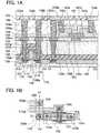
- FIGS. 1A and 1Bthe structure and the manufacturing method of a semiconductor device will be described with reference to FIGS. 1A and 1B , FIG. 2 , FIGS. 3A and 3B , FIGS. 4A to 4H , FIGS. 5A to 5G , and FIGS. 6A to 6D .
- FIG. 1Ashows a cross-sectional view of the semiconductor device according to this embodiment.
- FIG. 1Bshows a plane view of the semiconductor device according to this embodiment.
- FIG. 1Acorresponds to section A1-A2 and D1-D2 shown in FIG. 1B .
- the semiconductor device shown in FIGS. 1A and 1Bincludes a p-type transistor 160 in its lower part and an n-type transistor 162 using an oxide semiconductor in its upper part.
- the p-type transistor 160includes a channel formation region 116 in a substrate 100 containing a semiconductor material; impurity regions 114 and heavily doped regions 120, a combination of the impurity regions 114 and the heavily doped regions 120 can simply be referred to as impurity regions, impurity regions between which is interposed the channel formation region 116; a gate insulating layer 108a over the channel formation region 116; a gate electrode 110a over the gate insulating layer 108a; a source or drain electrode 130a electrically connected to a first impurity region 114 on one side of the channel formation region 116; and a source or drain electrode 130b electrically connected to a second impurity region 114 on another side of the channel formation region 116.
- side wall insulating layers 118are formed on the sides of the gate electrode 110a. Moreover, at least parts of the side wall insulating layers 118 are comprised between the heavily doped regions 120 formed in regions of the substrate 100, when seen from above, and metal compound regions 124 are present over the heavily doped regions 120. Further, an element insulation insulating layer 106 is formed over the substrate 100 so as to surround the p-type transistor 160, and an interlayer insulating layer 126 and an interlayer insulating layer 128 are formed so as to cover the p-type transistor 160.
- the source or drain electrode 130ais electrically connected to a first metal compound region 124 on the one side of the channel formation region 116, and the source or drain electrode 130b is electrically connected to a second metal compound region 124 on the other side of the channel formation region 116 through openings in the interlayer insulating layer 126 and the interlayer insulating layer 128.
- the source or drain electrode 130ais electrically connected to a first heavily doped region 120 and to the first impurity region 114 which are on the one side of the channel formation region 116 through the first metal compound region 124 on the one side of the channel formation region 116
- the source or drain electrode 130bis electrically connected to a second heavily doped region 120 and to the second impurity region 114 which are on the other side of the channel formation region 116 through the second metal compound region 124 on the other side the channel formation region 116.
- the n-type transistor 162includes a gate electrode 136c over the interlayer insulating layer 128; a gate insulating layer 138 over the gate electrode 136c; an oxide semiconductor layer 140 over the gate insulating layer 138; and a source or drain electrode 142a and a source or drain electrode 142b which are over the oxide semiconductor layer 140 and electrically connected to the oxide semiconductor layer 140.
- the gate electrode 136c of the n-type transistor 162is formed so as to be embedded in an insulating layer 132 which is over the interlayer insulating layer 128. Further, as in the case of the gate electrode 136c, an electrode 136a and an electrode 136b are formed so as to be on the source and drain electrodes 130a and 130b of the p-type transistor 160.
- a protective insulating layer 144is formed over the n-type transistor 162 so as to be in contact with part of the oxide semiconductor layer 140.
- An interlayer insulating layer 146is formed over the protective insulating layer 144.
- the protective insulating layer 144 and the interlayer insulating layer 146are provided with openings reaching the source or drain electrode 142a and the source or drain electrode 142b.
- An electrode 150c and an electrode 150dare each in contact with one of the source or drain electrode 142a and the source or drain electrode 142b through the openings.
- an electrode 150a and an electrode 150bare formed in contact with the electrode 136a and the electrode 136b, respectively, through openings in the gate insulating layer 138, the protective insulating layer 144, and the interlayer insulating layer 146.
- the oxide semiconductor layer 140is preferably of high purity, produced by adequate removal of an impurity such as hydrogen.
- the hydrogen concentration of the oxide semiconductor layer 140is 5 ⁇ 10 19 atoms/cm 3 or less.
- the hydrogen concentration of the oxide semiconductor layer 140is 5 ⁇ 10 18 atoms/cm 3 or less, and more preferably 5 ⁇ 10 17 atoms/cm 3 or less.
- the n-type transistor 162can have excellent off-state current characteristics by using the oxide semiconductor layer 140 with high purity produced by an adequate reduction in hydrogen concentration. For example, when the drain voltage Vd is +1 or +10 V and the gate voltage Vg ranges from -20 to -5 V, the off-state current is 1 ⁇ 10 -13 A or less.
- the off-state current of the n-type transistor 162is reduced by the use of the oxide semiconductor layer 140 with high purity produced by an adequate reduction in hydrogen concentration, thereby leading to a semiconductor device having excellent characteristics.
- the above hydrogen concentration of the oxide semiconductor layerwas measured by SIMS (secondary ion mass spectroscopy).
- An insulating layer 152is formed over the interlayer insulating layer 146.
- An electrode 154a, an electrode 154b, and an electrode 154care formed so as to be embedded in the insulating layer 152.
- the electrode 154ais in contact with the electrode 150a
- the electrode 154bis in contact with the electrodes 150b and 150c
- the electrode 154cis in contact with the electrode 150d.
- the source or drain electrode 130b of the p-type transistor 160is electrically connected to the source or drain electrode 142a of the n-type transistor 162 through the electrode 136b, the electrode 150b, the electrode 154b, and the electrode 150c.
- the gate electrode 110a of the p-type transistor 160is electrically connected to the gate electrode 136c of the n-type transistor 162 through the electrodes built in the interlayer insulating layer 126 and the interlayer insulating layer 128.
- the source or drain electrode 130a of the p-type transistor 160is electrically connected, through the electrode 154a, the electrode 150a, and the electrode 136a, to the power supply line for supplying a first potential.
- the source or drain electrode 142b of the n-type transistor 162is electrically connected, through the electrode 154c and the electrode 150d, to the power supply line for supplying a second potential.
- FIG. 2shows an equivalent circuit of a CMOS inverter circuit in which the p-type transistor 160 is connected to the n-type transistor 162 in a complementary manner.
- FIG. 2shows an example of the semiconductor device illustrated in FIGS. 1A and 1B in which the positive potential VDD is applied to the electrode 154a and the ground potential GND is applied to the electrode 154c. Note that the ground potential GND can be also referred to as the negative potential VDL.
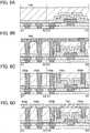
- FIG. 3Ashows a cross-sectional view of a p-type transistor 164 in the lower part and an n-type transistor 166 using an oxide semiconductor in the upper part.
- FIG. 3Bshows a plane view of the same. Note that FIG. 3A is a cross-sectional view showing section B1-B2 and section C1-C2 in FIG. 3B .
- FIGS. 3A and 3Bthe same components as those in FIGS. 1A and 1B are denoted by the same reference numerals as those of FIGS. 1A and 1B .
- a source or drain electrode 130c and source or drain electrode 130d of the p-type transistor 164are electrically connected to an electrode 136d and an electrode 136e, respectively, which are formed so as to embed themselves in the insulating layer 132.
- the electrode 136d and the electrode 136eare electrically connected to an electrode 150e and an electrode 150f, respectively, which are formed so as to be embedded in the gate insulating layer 138, the protective insulating layer 144, and the interlayer insulating layer 146.
- the electrode 150e and the electrode 150fare respectively electrically connected to the electrode 154d and the electrode 154e which are formed so as to be embedded in the insulating layer 152.
- the source or drain electrode 130c of the p-type transistor 164is electrically connected, through the electrode 136d, the electrode 150e, and the electrode 154d, to a power supply line which supplies a first potential
- the source or drain electrode 130dis electrically connected, through the electrode 136e, the electrode 150f, and the electrode 154e, to the power supply line which supplies a second potential. Therefore, the p-type transistor 164 can be used alone.
- a gate insulating layer 108bis formed over the element insulation insulating layer 106.
- a gate wiring 110bis provided over the gate insulating layer 108b.
- the gate wiring 110bis electrically connected to an electrode 130e formed so as to be embedded in the interlayer insulating layer 126 and the interlayer insulating layer 128.
- the electrode 130eis electrically connected to a gate electrode 136f formed so as to be embedded in the insulating layer 132.
- the gate electrode 136f of the n-type transistor 166is electrically connected to the gate wiring 110b through the electrode 130e, so that the n-type transistor 166 can be used alone.
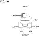
- a substrate 100 which contains a semiconductor materialis prepared (see FIG. 4A ).
- a single crystal semiconductor substrate of silicon, carbon silicon, or the like; a microcrystalline semiconductor substrate; a compound semiconductor substrate of silicon germanium or the like; an SOI substrate, or the likecan be used as the substrate 100 which contains a semiconductor material.
- SOI substratemeans a semiconductor substrate having a silicon semiconductor layer over its insulating surface.
- SOI substratealso means a substrate having a semiconductor layer using a material other than silicon over its insulating surface.
- a semiconductor layer included in the "SOI substrate”is not limited to a silicon semiconductor layer.
- the SOI substrateinclude an insulating substrate such as glass having a semiconductor layer over its surface, with an insulating layer between the semiconductor layer and the insulating substrate.
- a protective layer 102 that serves as a mask for forming an insulating element insulating layeris formed over the substrate 100 (see FIG. 4A ).
- an impurity element giving n-type conductivity or an impurity element giving p-type conductivitycan be added to the substrate 100 in order to control the threshold voltage of the transistor.
- siliconis used as the semiconductor
- phosphorus, arsenic, or the likecan be used as an impurity giving n-type conductivity.
- boron, aluminum, gallium, or the likecan be used as an impurity giving p-type conductivity.
- a region of the substrate 100 which is not covered with the protective layer 102 (exposed region)is etched using the protective layer 102 as a mask.
- an isolated semiconductor region 104is formed (see FIG. 4B ).
- dry etchingis preferably employed as the etching
- wet etchingcan also be employed as the etching.
- An etching gas and an etchantcan be selected as appropriate in accordance with a material of layers to be etched.
- an insulating layeris formed so as to cover the semiconductor region 104 and a region of the insulating layer which overlaps with the semiconductor region 104 is selectively etched, forming element insulation insulating layer 106 (see FIG. 4B ).
- the insulating layeris formed using silicon oxide, silicon nitride, silicon nitride oxide, or the like. Methods for removing the insulating layer over the semiconductor region 104 include etching, polishing such as CMP, and the like, and any of these are applicable. Note that after the semiconductor region 104 is formed or after the element insulation insulating layer 106 are formed, the protective layer 102 is removed.
- an insulating layeris formed over the semiconductor region 104, and a layer containing a conductive material is formed over the insulating layer.
- the insulating layerwhich is to be a gate insulating layer, has a single-layer structure or a layered structure of films containing silicon oxide, silicon nitride oxide, silicon nitride, hafnium oxide, aluminum oxide, tantalum oxide, or the like obtained by CVD, sputtering, or the like.
- the insulating layercan be formed by oxidizing or nitriding a surface of the semiconductor region 104 by high-density plasma treatment or thermal oxidation treatment.
- the high-density plasma treatmentcan be performed using a rare gas such as He, Ar, Kr, or Xe and a mixed gas of oxygen, nitrogen oxide, ammonia, nitrogen, hydrogen, or the like, for example.
- the thickness of the insulating layercan range from 1 to 100 nm, for example.
- the layer containing a conductive materialcan be formed using a metal material such as aluminum, copper, titanium, tantalum, and tungsten.
- the layer containing a conductive materialcan be formed using a semiconductor material such as polycrystalline silicon containing a conductive material.
- a variety of deposition methodssuch as vapor deposition, CVD, sputtering, and spin coating are applicable. Note that in this embodiment, an example of a case where the layer containing a conductive material is formed using a metal material is described.
- the insulating layer and the layer containing a conductive materialare selectively etched, thereby forming a gate insulating layer 108a and a gate electrode 110a (see FIG. 4C ).
- the gate wiring 110b shown in FIGS. 3A and 3Bcan be formed in the same formation step here.
- an insulating layer 112 which covers the gate electrode 110ais formed (see FIG. 4C ).
- boron (B), aluminum (Al), or the likeis added to the semiconductor region 104, forming impurity regions 114 with a shallow junction depth (see FIG. 4C ).
- the concentration of the added impuritycan be set as appropriate; the concentration is preferably raised in accordance with the degree of miniaturization of the semiconductor element.
- a process in which the impurity regions 114 are formed after the insulating layer 112 is formedis employed; alternatively, a process in which the insulating layer 112 is formed after the impurity regions 114 are formed can be employed.
- side wall insulating layers 118are formed (see FIG. 4D ).
- the side wall insulating layers 118can be formed in a self-aligned manner by forming an insulating layer covering the insulating layer 112 and then performing highly anisotropic etching on the insulating layer.
- the insulating layer 112is partly etched, so that a top surface of the gate electrode 110a and a top surface of the impurity regions 114 are exposed.
- an insulating layeris formed so as to cover the gate electrode 110a, the impurity regions 114, the side wall insulating layers 118, and the like. Then, boron (B), aluminum (Al), or the like is added to a region where the insulating layer is in contact with the impurity regions 114, thereby forming heavily doped regions 120 (see FIG. 4E ). After that, the insulating layer is removed, and a metal layer 122 is formed so as to cover the gate electrode 110a, the side wall insulating layers 118, the heavily doped regions 120, and the like (see FIG. 4E ).
- the metal layer 122can be formed by a variety of methods, such as vapor deposition, sputtering, and spin coating.
- the metal layer 122be formed using a metal material which, by reacting with a semiconductor material included in the semiconductor region 104, may become a metal compound having low resistance.
- metal materialsinclude titanium, tantalum, tungsten, nickel, cobalt, and platinum.
- metal compound regions 124which are in contact with the heavily doped regions 120 are formed (see FIG. 4F ). Note that when the polycrystalline silicon or the like is used for the gate electrode 110a, a metal compound region is also formed in a portion where the gate electrode 110a is in contact with the metal layer 122.
- irradiation with a flash lampcan be used for the above heat treatment.
- another heat treatmentis acceptable; a method which realizes brief periods of heat treatment is preferably used in order to improve the controllability of chemical reaction relating to the formation of the metal compound.
- the metal compound regionshave adequately high conductivity because they are formed by the reaction of the metal material and the semiconductor material.
- the metal compound regionscan adequately reduce electric resistance and improve element characteristics.
- the metal layer 122is removed after the metal compound regions 124 are formed.
- an interlayer insulating layer 126 and an interlayer insulating layer 128are formed so as to cover the elements formed in the above steps (see FIG. 4G ).
- the interlayer insulating layers 126 and 128can be formed using a material including an inorganic insulating material, such as silicon oxide, silicon nitride oxide, silicon nitride, hafnium oxide, aluminum oxide, and tantalum oxide. Alternatively, an organic insulating material such as polyimide and acrylic can be used. Although the interlayer insulating layer 126 and the interlayer insulating layer 128 form a two-layer structure here, the structure of the interlayer insulating layers is not limited to this. After the interlayer insulating layer 128 is formed, a surface thereof is preferably flattened by CMP, etching, or the like.
- a source or drain electrode 130a and a source or drain electrode 130bare formed in the openings (see FIG. 4H ).
- the source or drain electrode 130a and the source or drain electrode 130bare formed in the following manner: a conductive layer is formed in a region including the openings by PVD, CVD, or the like, and then, the conductive layer is partly removed by etching or CMP.
- the source or drain electrode 130a and the source or drain electrode 130bare formed by removing part of the conductive layer, it is preferable that a surface thereof be processed to be flat.
- CMP performed afterwardscan remove unnecessary part of the tungsten film, titanium film, titanium nitride film, and the like, and improve the flatness of the surface.
- Adequate electrodes, wirings, insulating layers, semiconductor layers, or the likecan be formed in the later steps by such an improvement in the flatness of a surface of the source or drain electrode 130a and source or drain electrode 130b.
- a wiring which is to be in contact with the gate electrode 110a or the likecan be formed in the same formation step. Further, at that time, the connection electrode 130e which is in contact with the gate wiring 110b shown in FIGS. 3A and 3B can be formed.
- the material for the source or drain electrode 130a and the source or drain electrode 130ba variety of conductive materials are applicable. For example, a conductive material such as molybdenum, titanium, chromium, tantalum, tungsten, aluminum, copper, neodymium, and scandium is applicable.
- the above processallows a p-type transistor using the substrate 100 containing a semiconductor material to be formed. After the above process, an additional wiring or the like can be formed. Multilayer interconnection structure using a layered structure of an interlayer insulating layer and a conductive layer provides a highly integrated semiconductor device.
- FIGS. 5A to 5G and FIGS. 6A to 6Dillustrate the manufacturing method of the n-type transistor and show a cross-sectional views along section A1-A2 and section D1-D2 in FIGS. 1A and 1B . Note that the p-type transistor which is below the n-type transistor is omitted in FIGS. 5A to 5G and FIGS. 6A to 6D .
- an insulating layer 132is formed over the interlayer insulating layer 128, the source or drain electrode 130a, and the source or drain electrode 130b (see FIG. 5A ).
- the insulating layer 132can be formed by PVD, CVD, or the like.
- the insulating layer 132can be formed using a material containing an inorganic insulating material such as silicon oxide, silicon nitride oxide, silicon nitride, hafnium oxide, aluminum oxide, and tantalum oxide.
- an opening reaching the source or drain electrode 130a, and an opening reaching the source or drain electrode 130bare formed in the insulating layer 132. At that time, an additional opening is formed in a region where a gate electrode will be formed. Then, a conductive layer 134 is formed so as to fill the openings (see FIG. 5B ).
- the openingscan be formed by etching or the like using a mask.
- the maskcan be made by exposures using a photomask, for example. Either wet etching or dry etching can be used as the etching; in view of the fine patterning, dry etching is preferable.
- the conductive layer 134can be formed by a deposition method such as PVD and CVD.
- Examples of the material for the conductive layer 134include a conductive material such as molybdenum, titanium, chromium, tantalum, tungsten, aluminum, copper, neodymium, and scandium; and an alloy and compound (e.g. nitride) of any of these materials.
- a conductive materialsuch as molybdenum, titanium, chromium, tantalum, tungsten, aluminum, copper, neodymium, and scandium
- an alloy and compounde.g. nitride
- the methodcan employ a thin titanium film formed by PVD in a region including openings, a thin titanium nitride film formed by CVD, and a tungsten film formed so as to fill the openings.
- the titanium film formed by PVDhas a function of reducing an oxide film at an interface with a lower electrode (here, the source or drain electrode 130a or the source or drain electrode 130b), and thus reducing contact resistance to the lower electrode.
- the titanium nitride film to be formed afterwardshas a barrier function of blocking diffusion of the conductive material.
- the conductive layer 134After the conductive layer 134 is formed, part of the conductive layer 134 is removed by etching or CMP, and the insulating layer 132 is thus exposed, thereby forming an electrode 136a, an electrode 136b, and a gate electrode 136c (see FIG. 5C ). Note that when the electrode 136a, the electrode 136b, the gate electrode 136c are formed by removing part of the conductive layer 134, it is preferable that a surface of the insulating layer 132, the electrode 136a, the electrode 136b, and the gate electrode 136c be processed to be flat.
- Adequate electrodes, wirings, insulating layers, semiconductor layers, or the likecan be formed in the later steps by such an improvement in the flatness of a surface of the insulating layer 132, the electrode 136a, the electrode 136b, and the gate electrode 136c.
- a gate insulating layer 138is formed so as to cover the insulating layer 132, the electrode 136a, the electrode 136b, and the gate electrode 136c (see FIG. 5D ).
- the gate insulating layer 138can be formed by CVD, sputtering, or the like.
- the gate insulating layer 138preferably contains silicon oxide, silicon nitride, silicon oxynitride, silicon nitride oxide, aluminum oxide, or the like. Note that the gate insulating layer 138 has either a single-layer structure or a layered structure.
- the gate insulating layer 138 of silicon oxynitridecan be formed by plasma CVD using silane (SiH 4 ), oxygen, and nitrogen as a source gas.
- the thickness of the gate insulating layer 138there is no particular limitation on the thickness of the gate insulating layer 138; the thickness can range from 20 to 500 nm, for example.
- the gate insulating layer 138preferably has a first gate insulating layer with a thickness ranging from 50 to 200 nm and a second gate insulating layer with a thickness ranging from 5 to 300 nm which is over the first gate insulating layer.
- an i-type or substantially i-type oxide semiconductor achieved by the removal of impuritiesis extremely sensitive to interface state density or interface charge. Therefore, an interface between an oxide semiconductor layer and a gate insulating layer is an important factor in the case where such an oxide semiconductor is used for the oxide semiconductor layer. In other words, the gate insulating layer 138 which is in contact with an oxide semiconductor layer of high purity needs to be of high quality.
- high-density plasma CVD using microwaves (2.45 GHz)is preferable in that it produces a compact high-quality gate insulating layer 138 of high withstand voltage. This is because a close contact between an oxide semiconductor layer with high purity and a high-quality gate insulating layer reduces interface state density and produces adequate interface characteristics.
- the insulating layercan be formed such that the quality of a gate insulating layer or interface characteristics between the gate insulating layer and an oxide semiconductor layer is improved.
- a layeris acceptable as long as the layer can be used for a gate insulating layer, can reduces interface state density between the gate insulating layer and the oxide semiconductor layer, and can provide a good interface.
- an oxide semiconductor layeris formed over the gate insulating layer 138, and the oxide semiconductor layer is processed by etching using a mask or the like, forming an island-shaped oxide semiconductor layer 140 (see FIG. 5E ).
- Such an oxide semiconductor layeris preferably an oxide semiconductor layer, especially an amorphous oxide semiconductor layer using one of an In-Ga-Zn-O-based oxide semiconductor, an In-Sn-Zn-O-based oxide semiconductor, an In-Al-Zn-O-based oxide semiconductor, a Sn-Ga-Zn-O-based oxide semiconductor, an Al-Ga-Zn-O-based oxide semiconductor, a Sn-Al-Zn-O-based oxide semiconductor, an In-Zn-O-based oxide semiconductor, a Sn-Zn-O-based oxide semiconductor, an Al-Zn-O-based oxide semiconductor, an In-O-based oxide semiconductor, a Sn-O-based oxide semiconductor, and a Zn-O-based oxide semiconductor.
- an amorphous oxide semiconductor layeris formed as the oxide semiconductor layer by sputtering, using an In-Ga-Zn-O-based oxide semiconductor target.
- the addition of silicon to an amorphous oxide semiconductor layersuppress the crystallization of the layer; therefore, the oxide semiconductor layer can be formed using a target containing SiO 2 at 2 to 10 wt. %.
- the filling factor of the target which is intended for the deposition of an oxide semiconductoris 90 to 100 %, and preferably 95 to 99.9 %.
- a target with a high filling factor which is intended for the deposition of an oxide semiconductorproduces a compact oxide semiconductor layer.
- the atmosphere for the depositionis preferably a rare gas (typically argon) atmosphere, an oxygen atmosphere, or a mixed atmosphere of a rare gas (typically argon) and oxygen.
- a high-purity gasin which the concentration of impurities such as hydrogen, water, hydroxyl, and hydride is reduced to approximately several parts per million (preferably several parts per billion), is preferable.
- a substrateis set in a chamber at reduced pressure and the substrate temperature is set to be comprised between 100 and 600 °C, and preferably between 200 and 400 °C.
- Depositing while heating the substratereduces the concentration of impurities contained in a deposited oxide semiconductor layer and also reduces damage to the layer due to sputtering.
- moisture remaining in the treatment chamberis removed at the same time as the introduction of a sputtering gas from which hydrogen and moisture are removed into the treatment chamber where a metal oxide is used as a target, thereby forming an oxide semiconductor layer.
- a sorption vacuum pumpis preferably used.
- a cryopump, an ion pump, or a titanium sublimation pumpcan be used.
- the evacuation unitcan be a turbo pump provided with a cold trap.
- a hydrogen atom, a compound containing a hydrogen atom, such as water (H 2 O), (more preferably also a compound containing a carbon atom), and the likeare removed from the deposition chamber when evacuated with a cryopump, thereby reducing the impurity concentration of the oxide semiconductor layer formed in the deposition chamber.
- the deposition conditionis as follows: the distance between a substrate and a target is 100 mm, the pressure is 0.6 Pa, the direct-current (DC) power is 0.5 kW, and the atmosphere is an oxygen atmosphere (the proportion of oxygen in the oxygen flow rate is 100 %).
- the use of a pulse direct-current (DC) power sourceis preferable in that it reduces powder substances (also referred to as particles or dust) which occur at the time of the deposition and in that it makes the film thickness even.
- the thickness of the oxide semiconductor layerpreferably ranges from 2 to 200 nm, and preferably 5 to 30 nm. Note that the appropriate thickness changes depending on the oxide semiconductor material used, and thus the thickness is selected as appropriate depending on the material used.
- the reverse sputteringmeans a method for improving the quality of a surface by ions striking the surface, while general sputtering is achieved by ions striking on a sputter target.
- Methods for making ions strike a surfaceinclude a method in which high frequency voltage is applied on the surface under an argon atmosphere and plasma is generated in the vicinity of the substrate. Note that a nitrogen atmosphere, helium atmosphere, oxygen atmosphere, or the like can be used instead of an argon atmosphere.
- the etching of the oxide semiconductor layercan be either dry etching or wet etching. Naturally, the etching can alternatively be a combination of dry etching and wet etching. Etching conditions (such as etching gas, etchant, etching time, and temperature) are appropriately adjusted in accordance with the material in order for the material to be etched into desired shapes.
- a gas containing chlorinea chlorine-based gas such as chlorine (Cl 2 ), triboron chloride (BCl 3 ), tetrasilicon chloride (SiCl 4 ), or tetracarbon tetrachloride (CCl 4 )
- a chlorine-based gassuch as chlorine (Cl 2 ), triboron chloride (BCl 3 ), tetrasilicon chloride (SiCl 4 ), or tetracarbon tetrachloride (CCl 4 )
- etching gasused for the dry etching.
- a gas containing fluorinea fluorine-based gas such as carbon tetrafluoride (CF 4 ), sulfur fluoride (SF 6 ), nitrogen fluoride (NF 3 ), or trifluoromethane (CHF 3 )); hydrogen bromide (HBr); oxygen (O 2 ); any of these gases to which a rare gas such as helium (He) or argon (Ar) is added; or the like can be used.
- a fluorine-based gassuch as carbon tetrafluoride (CF 4 ), sulfur fluoride (SF 6 ), nitrogen fluoride (NF 3 ), or trifluoromethane (CHF 3 )
- hydrogen bromideHBr
- oxygenO 2
- any of these gases to which a rare gassuch as helium (He) or argon (Ar) is added; or the like can be used.
- Parallel plate RIEreactive ion etching
- ICPinductively coupled plasma
- a mixed solution of phosphoric acid, acetic acid, and nitric acid, or the likecan be used as an etchant used for wet etching.
- ITO07Nby Kanto Chemical Co., Inc.
- ITO07Nby Kanto Chemical Co., Inc.
- the oxide semiconductor layeris subjected to a first heat treatment.
- the first heat treatmentallows the oxide semiconductor layer to be dehydrated or dehydrogenated.
- the temperature for the first heat treatmentis comprised between 300 and 750 °C, and is preferably 400 °C or more and less than the strain point of the substrate.
- a substrateis introduced into an electric furnace using a resistance heating element or the like, and the oxide semiconductor layer 140 is subjected to heat treatment at 450 °C for an hour under a nitrogen atmosphere. During the treatment, the oxide semiconductor layer 140 is not exposed to air to prevent contamination by water or hydrogen present in the air.
- the heat treatment apparatusis not limited to an electric furnace; the heat treatment apparatus can be an apparatus that heats an object using thermal conduction or thermal radiation given by a medium such as a heated gas or the like.
- an RTA (rapid thermal annealing) apparatussuch as a GRTA (gas rapid thermal annealing) apparatus or an LRTA (lamp rapid thermal annealing) apparatus is applicable.
- An LRTA apparatusis an apparatus that heats an object with radiation of light (an electromagnetic wave) emitted from a lamp such as a halogen lamp, a metal halide lamp, a xenon arc lamp, a carbon arc lamp, a high pressure sodium lamp, or a high pressure mercury lamp.
- a GRTA apparatusis an apparatus that performs heat treatment using a high-temperature gas.
- An inert gas which does not react with an object even during the heat treatment, such as nitrogen or a rare gas such as argonis used.
- the first heat treatmentcan employ GRTA, in which the substrate is moved into an inert gas heated at a high temperature of 650 to 700 °C, and heated for several minutes there, and then the substrate is moved out of the inert gas.
- GRTAenables short-time high-temperature heat treatment. Further, such a short-time heat treatment is applicable even at a temperature exceeding the strain point of the substrate.
- the first heat treatmentis preferably used an atmosphere which contains nitrogen or a rare gas (helium, neon, argon, or the like) as its main component and which does not contain water, hydrogen, or the like.
- nitrogen or a rare gassuch as helium, neon, or argon, which is introduced into the heat treatment apparatus
- the purity of nitrogen or a rare gas such as helium, neon, or argon, which is introduced into the heat treatment apparatusis preferably 6N (99.9999 %) or more, and preferably 7N (99.99999 %) or more (i.e. the impurity concentration is 1 ppm or less, and preferably 0.1 ppm or less).
- the oxide semiconductor layercrystallizes to be microcrystalline or polycrystalline depending on the conditions of the first heat treatment and the composition of the oxide semiconductor layer.
- the oxide semiconductor layercrystallizes to be a microcrystalline semiconductor layer with a degree of crystallization of 90 % or more, or 80 % or more in some cases.
- the oxide semiconductor layerbecomes an amorphous oxide semiconductor layer containing no crystalline component depending on the conditions of the first heat treatment and the composition of the oxide semiconductor layer.
- the oxide semiconductor layerbecomes an oxide semiconductor layer in which a microcrystalline portion (with a grain diameter of 1 to 20 nm, typically 2 to 4 nm) is mixed into an amorphous oxide semiconductor (e.g. a surface of the oxide semiconductor layer).
- a microcrystalline portionwith a grain diameter of 1 to 20 nm, typically 2 to 4 nm
- an amorphous oxide semiconductore.g. a surface of the oxide semiconductor layer.
- the electric characteristics of the oxide semiconductor layercan be changed by providing a microcrystalline portion where crystal grains of In 2 Ga 2 ZnO 7 having electrical anisotropy are aligned.
- the oxide semiconductor layerBy forming a microcrystalline portion where crystal grains of In 2 Ga 2 ZnO 7 are aligned at the surface of the oxide semiconductor layer, the oxide semiconductor layer exhibits an enhanced electrical conductivity in a direction parallel to the surface and an enhanced electrical resistivity in a direction perpendicular to the surface. Further, such a microcrystalline portion has the function of preventing impurities such as water and hydrogen from entering the oxide semiconductor layer.
- the above oxide semiconductor layercan be obtained by heating a surface of the oxide semiconductor layer by GRTA.
- the use of a sputter target that contains more In or Ga than Znallows the above oxide semiconductor layer to be formed in a preferable way.
- the first heat treatment performed on the oxide semiconductor layer 140can be performed on the oxide semiconductor layer not yet been processed into the island-shaped oxide semiconductor layer 140.
- the substrateis taken out from the heat treatment apparatus after the first heat treatment and then subjected to the photolithography process.
- the first heat treatmentcan also be called a dehydration process or dehydrogenation process because it is effective in dehydrating or dehydrogenating the oxide semiconductor layer 140. It is possible to perform such a dehydration process or dehydrogenation process after forming the oxide semiconductor layer, after forming a source or drain electrode layer over the oxide semiconductor layer 140, or after forming a protective insulating layer over the source or drain electrode. Such a dehydration process or dehydrogenation process can be conducted more than once.
- a source or drain electrode 142a and a source or drain electrode 142bare formed so as to be in contact with the oxide semiconductor layer 140 (see FIG. 5F ).
- the source or drain electrode 142a and the source or drain electrode 142bare formed by forming a conductive layer so that the conductive layer covers the oxide semiconductor layer 140 and then selectively etching the conductive layer.
- the conductive layercan be formed by PVD such as sputtering or CVD such as plasma CVD.
- the material for the conductive layerinclude an element selected from aluminum, chromium, copper, tantalum, titanium, molybdenum, and tungsten; and an alloy including any of these elements as a component.
- One or more of materials selected from manganese, magnesium, zirconium, beryllium, and thoriumcan be alternatively used for the conductive layer.
- aluminum combined with one or more of elements selected from titanium, tantalum, tungsten, molybdenum, chromium, neodymium, and scandiumcan be used for the conductive layer.
- the conductive layercan have either a single-layer structure or a layered structure of two or more layers.
- a single-layer structure of an aluminum film containing silicon, a two-layer structure in which a titanium film is stacked over an aluminum film, a three-layer structure in which a first titanium film, an aluminum film, and a second titanium film are stacked in this order, and the likecan be given as examples.
- the channel length (L) of the transistoris determined by the distance separating the source or drain electrode 142a and the source or drain electrode 142b on the oxide semiconductor 140.
- the channel length (L)is less than 25 nm, exposures for making a mask are performed in the extreme ultraviolet range of extremely short wavelength of several nanometers to several tens of nanometers. Exposures in the extreme ultraviolet range yield high resolution and a great depth of focus. Therefore, the channel length (L) of a transistor, which is formed later, can be 10 to 1000 nm, and thus the operation rate of the circuit can be increased. Further, since the off-state current is extremely low, the power consumption is not increased even in the case of fine patterning.
- the oxide semiconductor layer 140may be partly etched to be an oxide semiconductor layer having a groove (a depressed portion) depending on the composition of the oxide semiconductor layer and the etching conditions.
- An oxide conductive layercan be formed between the oxide semiconductor layer 140 and the source or drain electrode 142a or between the oxide semiconductor layer 140 and the source or drain electrode 142b. It is possible to successively form the oxide conductive layer and a metal layer which is to be the source or drain electrode 142a or the source or drain electrode 142b (successive deposition).
- the oxide conductive layercan function as a source region or a drain region. Such an oxide conductive layer leads to the reduction in the electrical resistance of the source region or a drain region, and thus high-speed operation of the transistor is achieved.
- etchingcan be performed using a resist mask made by a gray-tone mask which is a light-exposure mask such that light transmitted by the mask has a plurality of intensities.
- a resist mask made by a gray-tone maskhas a plurality of thicknesses and can be further changed in shape by ashing; thus, such a resist mask can be used in a plurality of etching steps for different patterns.
- a resist mask applicable to at least two or more kinds of different patternscan be made by a single gray-tone mask. This reduces the number of exposure masks and also the number of corresponding photolithography steps, thereby simplifying the process.
- plasma treatment using a gas such as N 2 O, N 2 , and Aris preferably conducted after the above process.
- the plasma treatmentremoves water or the like that adheres to an exposed surface of the oxide semiconductor layer.
- the plasma treatmentcan use a mixed gas of oxygen and argon.
- a protective insulating layer 144 which is in contact with part of the oxide semiconductor layer 140is formed without exposure to air during the formation steps (see FIG. 5G ).
- the protective insulating layer 144is formed to a thickness of 1 nm or more and can be formed using as appropriate a method, such as sputtering, by which an impurity such as water or hydrogen is prevented from entering the protective insulating layer 144.
- Examples of the material for the protective insulating layer 144include silicon oxide, silicon nitride, silicon oxynitride, and silicon nitride oxide. Its structure can be either a single-layer structure or a layered structure.
- the substrate temperature for the deposition of the protective insulating layer 144is preferably room temperature or more and 300 °C or less.
- the atmosphere for the deposition of the protective insulating layer 144is preferably a rare gas (typically argon) atmosphere, an oxygen atmosphere, or a mixed atmosphere of a rare gas (typically argon) and oxygen.
- the mixing of hydrogen into the protective insulating layer 144causes contamination of the oxide semiconductor layer by hydrogen, the stripping of oxygen from the oxide semiconductor layer due to hydrogen, or the like, whereby the resistance of the backchannel of the oxide semiconductor layer may be reduced and a parasitic channel may be formed. Therefore, it is important not to use hydrogen when forming the protective insulating layer 144 in order to minimize entry of hydrogen in the protective insulating layer 144.
- the protective insulating layer 144it is preferable to form the protective insulating layer 144 while removing moisture remaining in the treatment chamber. This is in order to prevent hydrogen, hydroxyl, or water from entering the oxide semiconductor layer 140 and the protective insulating layer 144.
- a sorption vacuum pumpis preferably used.
- a cryopump, an ion pump, or a titanium sublimation pumpis preferably used.
- the evacuation unitcan be a turbo pump provided with a cold trap.
- a hydrogen atom, a compound containing a hydrogen atom, such as water (H 2 O), and the likeare removed from the deposition chamber when evacuated with the cryopump, thereby reducing the impurity concentration of the protective insulating layer 144 formed in the deposition chamber.
- a sputtering gas for the deposition of the protective insulating layer 144is preferably a high-purity gas in which the concentration of impurities such as hydrogen, water, hydroxyl, and hydride is reduced to approximately several parts per million (preferably approximately several parts per billion).
- a second heat treatmentis performed, preferably in an inert gas atmosphere or oxygen gas atmosphere (preferably at 200 to 400 °C, e.g. 250 to 350 °C).
- the second heat treatmentis performed in a nitrogen atmosphere at 250 °C for one hour.
- the second heat treatmentcan reduce variations between transistors in electric characteristics.
- Heat treatmentcan be performed at 100 to 200 °C for 1 to 30 hours in an air atmosphere. This heat treatment can be performed at a fixed heating temperature or follow temperature cycles where the temperature repeatedly rises from room temperature to a heating temperature of 100 to 200 °C and drops from the a heating temperature to room temperature. This heat treatment can be performed before the deposition of the protective insulating layer under a reduced pressure. Heat treatment under reduced pressure shortens the heating time. Note that this heat treatment can be performed instead of the second heat treatment or after the second heat treatment.
- an interlayer insulating layer 146is formed over the protective insulating layer 144 (see FIG. 6A ).
- the interlayer insulating layer 146can be formed by PVD, CVD, or the like.
- the interlayer insulating layer 146can be formed using a material containing an inorganic insulating material, such as silicon oxide, silicon nitride oxide, silicon nitride, hafnium oxide, aluminum oxide, and tantalum oxide.
- a surface thereofis preferably flattened by CMP, etching, or the like.
- openings reaching the electrode 136a, the electrode 136b, the source or drain electrode 142a, and the source or drain electrode 142bare formed in the interlayer insulating layer 146, the protective insulating layer 144, and the gate insulating layer 138.
- a conductive layer 148is formed so as to be embedded in the openings (see FIG. 6B ).
- the openingscan be formed by etching using a mask.
- the maskcan be made by exposures using a photomask, for example. Either wet etching or dry etching can be used as the etching; in case of a fine patterning, dry etching is preferably used.
- the conductive layer 148can be formed by a deposition method such as PVD and CVD.
- Examples of the material for the conductive layer 148include a conductive material such as molybdenum, titanium, chromium, tantalum, tungsten, aluminum, copper, neodymium, and scandium; and an alloy and compound (e.g. nitride) of any of these materials.
- a conductive materialsuch as molybdenum, titanium, chromium, tantalum, tungsten, aluminum, copper, neodymium, and scandium
- an alloy and compounde.g. nitride
- the methodcan employ a thin titanium film formed by PVD in a region including openings, a thin titanium nitride film formed by CVD, and a tungsten film formed so as to fill the openings.
- the titanium film formed by PVDhas a function of reducing an oxide film at an interface with a lower electrode (here, the electrode 136a, the electrode 136b, the source or drain electrode 142a, or the source or drain electrode 142b), and thus reducing contact resistance to the lower electrode.
- the titanium nitride film to be formedafterwards a barrier function of blocking the diffusion of the conductive material.
- the conductive layer 148After the conductive layer 148 is formed, part of the conductive layer 148 is removed by etching or CMP, and the interlayer insulating layer 146 is thus exposed, thereby forming the electrode 150a, the electrode 150b, the electrode 150c, and the electrode 150d (see FIG. 6C ). Note that when the electrode 150a, the electrode 150b, the electrode 150c, and the electrode 150d are formed by removing part of the conductive layer 148, it is preferable that a surface be processed to be flat.
- Adequate electrodes, wirings, insulating layers, semiconductor layers, or the likecan be formed in the later steps by such an improvement in the flatness of a surface of the interlayer insulating layer 146, the electrode 150a, the electrode 150b, the electrode 150c, and the electrodes 150d.
- an insulating layer 152is formed, and openings reaching the electrode 150a, the electrode 150b, the electrode 150c, and the electrode 150d are formed in the insulating layer 152. Then, a conductive layer is formed so as to fill the openings. After that, part of the conductive layer is removed by etching or CMP, and the insulating layer 152 is thus exposed, thereby forming an electrode 154a, an electrode 154b, and an electrode 154c (see FIG. 6D ). This process is similar to that of forming the electrode 150a and the like previously described, and the details are therefore omitted.
- the hydrogen concentration of the oxide semiconductor layer 140is 5 ⁇ 10 19 atoms/cm 3 or less, and the off-state current of the n-type transistor 162 is 1 ⁇ 10 -13 A or less, and preferably 100 zA/ ⁇ m or less.
- the use of such an oxide semiconductor layer 140 with high purity produced by an adequate reduction in hydrogen concentrationproduces the n-type transistor 162 having excellent characteristics and also produces a semiconductor device having excellent characteristics which has a p-type transistor in its lower part and an n-type transistor using an oxide semiconductor in its upper part.
- a combination of a transistor using a material other than an oxide semiconductor and a transistor using an oxide semiconductorallows for the production of a semiconductor device requiring electric characteristics different from those of transistors using an oxide semiconductor (e.g. difference in carriers characteristics, which have an effect on the behavior of the element).
- a transistor using an oxide semiconductorhas good switching characteristics, so that an excellent semiconductor device utilizing these characteristics can be made.
- a CMOS inverter circuitcan adequately reduce flow-through current, thereby reducing the power consumption of the semiconductor device and preventing damage to the semiconductor device due to a heavy current.
- a transistor using an oxide semiconductorhas extremely low off-state current, thereby reducing the power consumption of the semiconductor device.
- the semiconductor device according to this embodimentis not limited to this; the p-type transistor 160 and the n-type transistor 162 can be formed over the same substrate.
- the case where the channel length direction of the p-type transistor 160 is perpendicular to the channel length direction of the n-type transistor 162is described as an example, the physical relationship between the p-type transistor 160 and the n-type transistor 162 is not limited to this.
- the p-type transistor 160 and the n-type transistor 162can overlap with each other.
- FIGS. 7A and 7B and FIG. 8the structure of a semiconductor device according to the disclosed invention is described with reference to FIGS. 7A and 7B and FIG. 8 . Note that in this embodiment, the structure of a semiconductor device which can be used as a memory element is described.
- FIG. 7Ashows a cross-sectional view of a semiconductor device according to this embodiment.
- FIG. 7Bshows a plane view of the semiconductor device according to this embodiment.
- FIG. 7Ashows section E1-E2 and section F1-F2 of FIG. 7B .
- the semiconductor device shown in FIGS. 7A and 7Bincludes a transistor 260 in its lower part, which is formed using silicon, and a transistor 262 in its upper part, which is formed using an oxide semiconductor.
- the transistor 260 using siliconincludes: a channel formation region 216 in a substrate 200 containing silicon, impurity regions 214 and heavily doped regions 220, collectively called simply impurity regions, impurity regions between which is interposed the channel formation region 216, a gate insulating layer 208a over the channel formation region 216; a gate electrode 210a over the gate insulating layer 208a; a source or drain electrode 230a electrically connected to a first impurity region 214 on one side of the channel formation region 216; and a source or drain electrode 230b electrically connected to a second impurity region 214 on another side of the channel formation region 216.
- the source or drain electrode 230ais electrically connected to the first impurity region 214 on the one side of the channel formation region 216 through a first metal compound region 224 on the one side of the channel formation region 216
- the source or drain electrode 230bis electrically connected to the second impurity region 214 on the other side of the channel formation region 216 through a second metal compound region 224 on the other side the channel formation region 216.
- the structure of the transistor 260is similar to that of the p-type transistor 160 described in Embodiment 1, and thus other details of the transistor 260 can be seen in Embodiment 1.
- the transistor 260can be either a p-type transistor or an n-type transistor.
- the transistor 262 using an oxide semiconductorincludes: a gate electrode 236c over an insulating layer 228, a gate insulating layer 238 over the gate electrode 236c, an oxide semiconductor layer 240 over the gate insulating layer 238, and source or drain electrodes 242a and 242b which are over the oxide semiconductor layer 240 and electrically connected to the oxide semiconductor layer 240.
- the structure of the transistor 262is similar to that of the n-type transistor 162 described in Embodiment 1, and thus other details of the transistor 262 can be seen in Embodiment 1.
- the transistor 262can be either an n-type transistor or a p-type transistor.
- the source or drain electrode 230a in the transistor 260is electrically connected to a first wiring through an electrode 236a, an electrode 250a, an electrode 254a, and the like.
- the source or drain electrode 230b in the transistor 260is electrically connected to a second wiring through an electrode 236b, an electrode 250b, an electrode 254b, and the like.
- the source or drain electrode 242a of the transistor 262is electrically connected to the gate electrode 210a of the transistor 260 through an electrode 250d, an electrode 254c, an electrode 250c, an electrode 236b, and an electrode 230c.
- the source or drain electrode 242b of the transistor 262is electrically connected to a third wiring through an electrode 250e, an electrode 254d, and the like.
- an element isolation insulating layer 206corresponds to the element insulation insulating layer 106 in Embodiment 1; side wall insulating layers 218 to the side wall insulating layers 118 in Embodiment 1; an interlayer insulating layer 226 to the interlayer insulating layer 126 in Embodiment 1; an insulating layer 232 to the insulating layer 132 in Embodiment 1; a protective insulating layer 244 to the protective insulating layer 144 in Embodiment 1; an interlayer insulating layer 246 to the interlayer insulating layer 146 in Embodiment 1; and an insulating layer 252 to the insulating layer 152 in Embodiment 1.
- the insulating layer 228 or the interlayer insulating layer 246is an aluminum oxide layer.
- FIG. 8shows an example of the diagram of a circuit using the above semiconductor device as a memory element.
- the source electrode of the transistor 260 using siliconis electrically connected to a first source wiring (Source 1).
- the drain electrode of the transistor 260 using siliconis electrically connected to a drain wiring (Drain).
- the gate electrode of the transistor 260 using siliconis electrically connected to the drain electrode of the transistor 262 using an oxide semiconductor.
- the source electrode of the transistor 262 using an oxide semiconductoris electrically connected to a second source wiring (Source 2).
- the gate electrode of the transistor 262 using an oxide semiconductoris electrically connected to a gate wiring (Gate).
- the transistor 262 using an oxide semiconductoris characterized by extremely low off-state current. Therefore, when the transistor 262 is placed in an off state, the potential of the gate electrode of the transistor 260 can be held for extremely long periods of time.
- the semiconductor devicecan serve as a memory element by making use of the characteristics of the transistor 262 which holds the potential of the gate electrode, for example by carrying out the following operation.
- the potential of the gate wiring (Gate)becomes a potential that turns on the transistor 262, and thus the transistor 262 is turned on.
- Thisallows the potential of the second source wiring (Source 2) to be applied to the gate electrode of the transistor 260 (write operation).
- the potential of the gate wiring (Gate)becomes a potential that turns off the transistor 262, and thus the transistor 262 is turned off.
- the potential of the gate electrode of the transistor 260can be held for extremely long periods of time. Specifically, for example, when the potential of the gate electrode of the transistor 260 is a potential that turns on the transistor 260, the transistor 260 is held in an on state for long periods of time. On the other hand, when the potential of the gate electrode of the transistor 260 is a potential that turns off the transistor 260, the transistor 260 is held in an off state for long periods of time.
- the value of the potential of the drain wiring (Drain)changes depending on the potential held by the gate electrode of the transistor 260.
- the potential of the gate electrode of the transistor 260is a potential that turns on the transistor 260
- the transistor 260is held in an on-state, so that the potential of the drain wiring (Drain) becomes equal to the potential of the first source wiring (Source 1).
- the value of the potential of the drain wiring (Drain)changes depending on the potential of the gate electrode of the transistor 260, and the semiconductor device serves as a memory element by reading this changing value (read operation).
- the semiconductor device according to this embodimentas a substantial non-volatile memory element because the semiconductor device enables data to be held for extremely long periods of time using the off-state current characteristics of the transistor 262.
- the structure of the semiconductor deviceis not limited to this. It is also possible to make a more developed semiconductor device with a plurality of memory elements interconnected to each other as appropriate. For example, it is possible to make a NAND-type or NOR-type semiconductor device by using more than one of the above memory elements. In addition, wiring connections are not limited to those in FIG. 8 and can be changed as appropriate.
- one embodiment of the present inventionforms a substantially non-volatile memory element using the off-state current characteristics of the transistor 262.
- one embodiment of the present inventionprovides a semiconductor device with a new structure.
- FIGS. 9A and 9B and FIG. 10the structure of a semiconductor device according to another embodiment of the disclosed invention is described with reference to FIGS. 9A and 9B and FIG. 10 . Note that in this embodiment, the structure of a semiconductor device which can be used as a memory element is described.
- FIG. 9Ashows a cross-sectional view of a semiconductor device according to this embodiment.
- FIG. 9Bshows a plane view of the semiconductor device according to this embodiment.
- FIG. 9Ashows section G1-G2 and section H1-H2 in FIG. 9B .
- the semiconductor device shown in FIGS. 9A and 9Bincludes, in its lower part, a p-type transistor 460 and an n-type transistor 464 which are formed using silicon, and includes, in its upper part, a transistor 462 using an oxide semiconductor.
- the p-type transistor 460 and the n-type transistor 464 which are formed using siliconhave a similar structure to that of the p-type transistor 160, the transistor 260, or the like in Embodiments 1 and 2.
- the transistor 462 using an oxide semiconductorhas a similar structure to that of the n-type transistor 162, the transistor 262, or the like in Embodiments 1 and 2. Therefore, the components of these transistors are also based on those of the transistors in Embodiments 1 and 2. The details can be seen in Embodiments 1 and 2.
- a substrate 400corresponds to the substrate 100 in Embodiment 1; an element isolation insulating layer 406 to the element insulation insulating layer 106 in Embodiment 1; a gate insulating layer 408a to the gate insulating layer 108a in Embodiment 1; a gate electrode 410a to the gate electrode 110a in Embodiment 1; a gate wiring 410b to the gate wiring 110b in Embodiment 1; impurity regions 414 to the impurity regions 114 in Embodiment 1; a channel formation region 416 to the channel formation region 116 in Embodiment 1; side wall insulating layers 418 to the side wall insulating layers 118 in Embodiment 1; heavily doped regions 420 to the heavily doped regions 120 in Embodiment 1; metal compound regions 424 to the metal compound regions 124 in Embodiment 1; an interlayer insulating layer 426 to the interlayer insulating layer 126 in Embodiment 1;
- an insulating layer 432corresponds to the insulating layer 132 in Embodiment 1; an electrode 436a to the electrode 136a in Embodiment 1; an electrode 436b to the electrode 136b in Embodiment 1; a gate electrode 436c to the gate electrode 136c in Embodiment 1; a gate insulating layer 438 to the gate insulating layer 138 in Embodiment 1; an oxide semiconductor layer 440 to the oxide semiconductor layer 140 in Embodiment 1; a source or drain electrode 442a to the source or drain electrode 142a in Embodiment 1; a source or drain electrode 442b to the source or drain electrode 142b in Embodiment 1; a protective insulating layer 444 to the protective insulating layer 144 in Embodiment 1; an interlayer insulating layer 446 to the interlayer insulating layer 146 in Embodiment 1; an electrode 450a to the electrode 150a in Embodiment 1; an electrode 450b to the electrode 150
- the semiconductor device according to this embodimentis different from the semiconductor device according to Embodiment 1 or 2 in having the drain electrode of the transistor 462, the gate electrode of the p-type transistor 460, and the gate electrode of the n-type transistor 464 electrically connected to each other (see FIGS. 9A and 9B ).
- This structureallows an input signal (INPUT) of the CMOS inverter circuit to be temporarily held.
- Examples of electronic appliances equipped with the semiconductor device according to any of Embodiments 1, 2, and 3are described with reference to FIGS. 11A to 11F .
- the semiconductor device according to any of Embodiments 1, 2, and 3includes a transistor using an oxide semiconductor with good switching characteristics, and thus can reduce the power consumption of the electronic appliance.
- a semiconductor device with a new structure using the characteristics of oxide semiconductorse.g. a memory element
- the semiconductor device according to any of Embodiments 1, 2, and 3can be mounted on a circuit substrate or the like alone or integrated with other components, and thus built into the electronic appliance.
- an integrated circuit into which the semiconductor device is integratedincludes a variety of circuit components such as a resistor, a capacitor, and a coil in addition to the semiconductor device according to any of Embodiments 1, 2, and 3.
- An example of the integrated circuitis a circuit into which an arithmetic circuit, a converter circuit, an amplifier circuit, a memory circuit, and circuits relating to any of these circuits are highly integrated. It can be said that MPUs (Microprocessor Units) and CPUs (Central Processing Units) are typical examples of the above.
- the semiconductor deviceis applicable to a switching element or the like in a display device.
- the semiconductor device and a driver circuitare preferably provided over the same substrate.
- the semiconductor deviceonly for a driver circuit of the display device.
- FIG. 11Ashows a notebook PC including the semiconductor device according to any of Embodiments 1, 2, and 3.
- the notebook PCincludes a main body 301, a housing 302, a display portion 303, a keyboard 304, and the like.
- FIG. 11Bshows a personal digital assistant (PDA) including the semiconductor device according to any of Embodiments 1, 2, and 3.
- the personal digital assistantincludes a main body 311 provided with a display portion 313, an external interface 315, operational keys 314, and the like.
- the personal digital assistantincludes a stylus 312 which is an accessory for operation.
- FIG. 11Cshows an electronic book 320 as an example of the electronic paper including the semiconductor device according to any of Embodiments 1, 2, and 3.
- the electronic book 320includes two housings: a housing 321 and a housing 323.
- the housing 321is combined with the housing 323 by a hinge 337, so that the electronic book 320 can be opened and closed using the hinge 337 as an axis.
- Such a structureallows the same use of the electronic book 320 as that of paper books.
- the housing 321includes a display portion 325, and the housing 323 includes a display portion 327.
- the display portion 325 and the display portion 327can display a continuous image or different images.
- the structure for displaying different imagesenables text to be displayed on the right display portion (the display portion 325 in FIG. 11C ) and images to be displayed on the left display portion (which is the display portion 327 in FIG. 11C ).
- FIG. 11Cshows an example of the case where the housing 321 includes an operating portion.
- the housing 321includes a power button 331, control keys 333, a speaker 335, and the like.
- the control keys 333allow pages to be turned.
- a keyboard, a pointing device, or the likecan also be provided on the same face as the display portion.
- an external connection terminalan earphone terminal, a USB terminal, a terminal connectable to various cables such as an AC adapter and a USB cable, or the like
- a recording medium insertion portion, and the likecan be provided on the back surface or a side surface of the housing.
- the electronic book 320can also serve as an electronic dictionary.
- the electronic book 320can send and receive information wirelessly. Through wireless communication, desired book data or the like can be purchased and downloaded from an electronic book server.
- electronic papercan be used for electronic appliances in all fields as long as they display data.
- electronic papercan be applied to posters, advertisement in vehicles such as trains, a variety of cards such as credit cards, and so on in addition to electronic books.
- FIG. 11Dshows a mobile phone including the semiconductor device according to any of Embodiments 1, 2, and 3.
- the mobile phoneincludes two housings: a housing 340 and a housing 341.
- the housing 341includes a display panel 342, a speaker 343, a microphone 344, a pointing device 346, a camera lens 347, an external connection terminal 348, and the like.
- the housing 340includes a solar cell 349 charging the mobile phone, an external memory slot 350, and the like.
- An antennais built in the housing 341.
- the display panel 342includes a touch panel.
- a plurality of control keys 345 which is displayed as an imageis shown by dashed lines in FIG. 11D .
- the mobile phoneincludes a booster circuit for increasing a voltage output from the solar cell 349 to a voltage needed for each circuit. It is possible for the mobile phone to have, in addition to the above structure, a structure in which a noncontact IC chip, a small recording device, or the like are formed.
- the display orientation of the display panel 342changes as appropriate in accordance with the application mode.
- the camera lens 347is provided on the same face as the display panel 342, so that the mobile phone can be used as a video phone.
- the speaker 343 and the microphone 344can be used for videophone calls, recording, and playing sound, etc. as well as voice calls.
- the housings 340 and 341 which are shown unfolded in FIG. 11Dcan overlap with each other by sliding. Thus, the mobile phone can be in a suitable size for portable use.
- the external connection terminal 348is connectable to an AC adaptor and a variety of cables such as a USB cable, which enables charging of the mobile phone and data communication between the mobile phone and a personal computer or the like. Moreover, a larger amount of data can be saved and moved by inserting a recording medium to the external memory slot 350.
- the mobile phonecan be capable of, in addition to the above, infrared communication, television reception, or the like.
- FIG. 11Eshows a digital camera including the semiconductor device according to any of Embodiments 1, 2, and 3.
- the digital cameraincludes a main body 361, a display portion A 367, an eyepiece 363, an operation switch 364, a display portion B 365, a battery 366, and the like.
- FIG. 11Fshows a television set including the semiconductor device according to any of Embodiments 1, 2, and 3.
- a television set 370has a housing 371 including a display portion 373. Images can be displayed on the display portion 373.
- the housing 371is supported by a stand 375.
- the television set 370can be operated by an operation switch included in the housing 371 or by a remote controller 380. Channels and volume can be controlled by a control key 379 included in the remote controller 380, and images displayed on the display portion 373 can thus be controlled. Further, the remote controller 380 can be provided with a display portion 377 displaying data from the remote controller 380.
- the television set 370preferably includes a receiver, a modem, and the like.
- the receiverallows the television set 370 to receive a general television broadcast.
- the television set 370is capable of one-way (from a transmitter to a receiver) or two-way (between a transmitter and a receiver, between receivers, or the like) data communication when connected to a communication network by wired or wireless connection via the modem.
Landscapes
- Thin Film Transistor (AREA)
- Metal-Oxide And Bipolar Metal-Oxide Semiconductor Integrated Circuits (AREA)
- Semiconductor Memories (AREA)
- Non-Volatile Memory (AREA)
- Electrodes Of Semiconductors (AREA)
- Internal Circuitry In Semiconductor Integrated Circuit Devices (AREA)
- Dram (AREA)
- Recrystallisation Techniques (AREA)
Description
- The technical field of the present invention relates to a semiconductor device. Note that here, semiconductor devices refer to general elements and devices which function utilizing semiconductor characteristics.
- There are a wide variety of metal oxides, and metal oxides have various applications. Indium oxide is a well-known material and has been used for transparent electrodes required in liquid crystal display devices or the like.
- Some metal oxides have semiconductor characteristics. Examples of metal oxides having semiconductor characteristics are tungsten oxide, tin oxide, indium oxide, zinc oxide, and the like. Thin film transistors having channel formation regions made of any of such metal oxides have already been described (e.g. see
Patent Documents 1 to 4 and Non-PatentDocument 1 etc.). - Incidentally, not only single-component oxides but also multi-component oxides are known as metal oxides. For example, homologous compounds InGaO3(ZnO)m (m is a natural number) are known multi-component oxides containing In, Ga and Zn (e.g. see Non-Patent Documents 2 to 4 and the like).
- An oxide semiconductor including such an In-Ga-Zn-based oxide is also known to be applicable to the channel forming layer of a thin film transistor (e.g. see Patent Document 5, Non-Patent Documents 5 and 6, and the like).
- Patent Document 6 discloses a high-performance highly integrated device in which bulk type FETs (field effect transistors) formed in a single crystalline silicon wafer and TFTs (thin film transistors) formed in a crystallised silicon film are three-dimensionally integrated. In a CMOS type SRAM structure according to an example, the TFTs are bottom-gate type TFTs.
- Patent document 7 discloses an SRAM with PFET devices comprising a polysilicon film on tungsten gates, stacked on NFET devices in a silicon substrate.
- [Patent Document 1] Japanese Published Patent Application No.
S60-198861 - [Patent Document 2] Japanese Published Patent Application No.
H8-264794 - [Patent Document 3] Japanese Translation of
PCT International Application H11-505377 - [Patent Document 4] Japanese Published Patent Application No.
2000-150900 - [Patent Document 5] Japanese Published Patent Application No.
2004-103957 - [Patent Document 6] Japanese Published Patent Application No.
H11-233789 - [Patent Document 7]
US Patent No. 5,112,765 - [Non-Patent Document 1]M. W. Prins, K. O. Grosse-Holz, G. Muller, J. F. M. Cillessen, J. B. Giesbers, R. P. Weening, and R. M. Wolf, "A ferroelectric transparent thin-film transistor", Appl. Phys. Lett., 17 June 1996, Vol. 68, p. 3650-3652
- [Non-Patent Document 2]M. Nakamura, N. Kimizuka, and T. Mohri, "The Phase Relations in the In2O3-Ga2ZnO4-ZnO System at 1350 °C", J. Solid State Chem., 1991, Vol. 93, p. 298-315
- [Non-Patent Document 3]Kimizuka, M. Isobe, and M. Nakamura, "Syntheses and Single-Crystal Data of Homologous Compounds, In2O3(ZnO)m (m = 3, 4, and 5), InGaO3(ZnO)3, and Ga2O3(ZnO)m (m = 7, 8, 9, and 16) in the In2O3-ZnGa2O4-ZnO System", J. Solid State Chem., 1995, Vol. 116, p. 170-178
- [Non-Patent Document 4] M. Nakamura, N. Kimizuka, T. Mohri, and M. Isobe, "Syntheses and crystal structures of new homologous compounds, indium iron zinc oxides (InFeO3(ZnO)m) (m:natural number) and related compounds", KOTAI BUTSURI (SOLID STATE PHYSICS), 1993, Vol. 28, No. 5, p. 317-327
- [Non-Patent Document 5]K. Nomura, H. Ohta, K. Ueda, T. Kamiya, M. Hirano, and H. Hosono, "Thin-film transistor fabricated in single-crystalline transparent oxide semiconductor", SCIENCE, 2003, Vol. 300, p. 1269-1272
- [Non-Patent Document 6] K. Nomura, H. Ohta, A. Takagi, T. Kamiya, M. Hirano, and H. Hosono, "Room-temperature fabrication of transparent flexible thin-film transistors using amorphous oxide semiconductors", NATURE, 2004, Vol. 432 p. 488-492
- Field-effect transistors, which are typical examples of semiconductor devices, are generally formed using a material such as silicon. However, semiconductor devices using silicon or the like do not have adequate switching characteristics; e.g. a problem is that a semiconductor device is damaged by a significantly high flow-through current in the case of the fabrication of a CMOS inverter circuit and that the power consumption is increased by a significantly high flow-through current.
- Moreover, the off-state current (also referred to as the leakage current) of semiconductor devices using silicon or the like is not as low as substantially zero. Therefore, a flow of slight current occurs without respect to the intended behavior of the semiconductor device, and thus it has been difficult to ensure an adequate period for charge retention in the case of the fabrication of a charge-retention semiconductor device such as memory or a liquid crystal display. A further problem is that the power consumption is increased by the off-state current.
- In view of this, an object of one embodiment of the present invention is to provide a semiconductor device with a new structure which solves the above problems.
- The present invention is directed to a semiconductor device as defined in
claim 1. Preferred embodiments are defined in the dependent claims. - Note that in this specification, the terms like "above" and "below" do not necessarily mean "directly above" and "directly below", respectively, in the description of a physical relationship between components. For example, the expression "a first gate electrode over a gate insulating layer" can correspond to a situation where there is an additional component between the gate insulating layer and the first gate electrode. The terms "above" and "below" are just used for convenience of explanations and they can be interchanged unless otherwise specified.
- In this specification, the term "electrode" or "wiring" does not limit the function of components. For example, an "electrode" can be used as part of a "wiring", and the "wiring" can be used as part of the "electrode". In addition, the term "electrode" or "wiring" can also mean a combination of a plurality of "electrodes" and "wirings", for example.
- In general, the term "SOI substrate" means a substrate having a silicon semiconductor layer over an insulating surface. In this specification, the term "SOI substrate" also means a substrate having a semiconductor layer using a material other than silicon over an insulating surface. In other words, a semiconductor layer included in the "SOI substrate" is not limited to a silicon semiconductor layer. In addition, a substrate in an "SOI substrate" is not limited to a semiconductor substrate such as a silicon wafer, and may be a non-semiconductor substrate such as a glass substrate, a quartz substrate, a sapphire substrate, and a metal substrate. In other words, "SOI substrates" also include a conductive substrate having an insulating surface or a substrate having a layer of a semiconductor material over an insulating substrate. In addition, in this specification and the like, a "semiconductor substrate" means a substrate of only a semiconductor material and also a general substrate of a material including a semiconductor material. In other words, in this specification, "SOI substrates" are also included in the broad category of semiconductor substrates.
- The present invention as defined in
claim 1 provides a semiconductor device including a transistor using silicon in its lower part, and a transistor using an oxide semiconductor in its upper part. - A combination of a transistor using silicon and a transistor using an oxide semiconductor allows for the production of a semiconductor device requiring electric characteristics different from those of transistors using an oxide semiconductor (e.g. difference in carriers characteristics, which have an effect on the behavior of the element).
- Further, a transistor using an oxide semiconductor has good switching characteristics, so that an excellent semiconductor device can be made utilizing these characteristics. Further, a transistor using an oxide semiconductor has extremely low off-state current, and the use of this transistor hence can reduce the power consumption of the semiconductor device.
FIG. 1A is a cross-sectional view illustrating a semiconductor device andFIG. 1B is a plane view thereof.FIG. 2 is a circuit diagram illustrating a semiconductor device.FIG. 3A is a cross-sectional view illustrating a semiconductor device andFIG. 3B is a plane view thereof.FIGS. 4A to 4H are cross-sectional views illustrating the manufacturing method of a semiconductor device.FIGS. 5A to 5G are cross-sectional views illustrating a manufacturing method of a semiconductor device.FIGS. 6A to 6D are cross-sectional views illustrating a manufacturing method of a semiconductor device.FIG. 7A is a cross-sectional view illustrating a semiconductor device andFIG. 7B is a plane view thereof.FIG. 8 is a circuit diagram illustrating a semiconductor device.FIG. 9A is a cross-sectional view illustrating a semiconductor device andFIG. 9B is a plane view thereof.FIG. 10 is a circuit diagram illustrating a semiconductor device.FIGS. 11A to 11F are diagrams for explaining electronic appliances using a semiconductor device.- Hereinafter, an "embodiment" not forming part of the claimed invention and embodiments of the claimed invention will be described with reference to the drawings. Specifically,
embodiment 1, despite of the term "embodiment", does not form part of the claimed invention. Embodiments 2 and 3 are embodiments of the claimed invention. Embodiment 4 is directed to electronic appliances equipped with the semiconductor device according toembodiments 1, 2 or 3. Depending on the semiconductor device comprised therein, the electronic appliances are therefore part of the claimed invention (embodiments 2 or 3) or not (embodiment 1). Note that the present invention is not limited to the following description, and it will be easily understood by those skilled in the art that various changes and modifications can be made without departing from the scope of the present invention. Thus, the present invention should not be interpreted as being limited to the following description of the embodiments. - Note that in some cases, the position, size, range of each component are not actual ones in the drawings and the like in order to facilitate understanding.
- Note that in this specification, ordinal numbers such as "first", "second", and "third" are used in order to avoid confusion among components, and the terms do not limit the components numerically.
- In this embodiment not forming part of the claimed invention, the structure and the manufacturing method of a semiconductor device will be described with reference to
FIGS. 1A and 1B ,FIG. 2 ,FIGS. 3A and 3B ,FIGS. 4A to 4H ,FIGS. 5A to 5G , andFIGS. 6A to 6D . FIG. 1A shows a cross-sectional view of the semiconductor device according to this embodiment.FIG. 1B shows a plane view of the semiconductor device according to this embodiment. Here,FIG. 1A corresponds to section A1-A2 and D1-D2 shown inFIG. 1B . The semiconductor device shown inFIGS. 1A and 1B includes a p-type transistor 160 in its lower part and an n-type transistor 162 using an oxide semiconductor in its upper part.- The p-
type transistor 160 includes achannel formation region 116 in asubstrate 100 containing a semiconductor material;impurity regions 114 and heavily dopedregions 120, a combination of theimpurity regions 114 and the heavily dopedregions 120 can simply be referred to as impurity regions, impurity regions between which is interposed thechannel formation region 116; agate insulating layer 108a over thechannel formation region 116; agate electrode 110a over thegate insulating layer 108a; a source ordrain electrode 130a electrically connected to afirst impurity region 114 on one side of thechannel formation region 116; and a source ordrain electrode 130b electrically connected to asecond impurity region 114 on another side of thechannel formation region 116. - Here, side
wall insulating layers 118 are formed on the sides of thegate electrode 110a. Moreover, at least parts of the sidewall insulating layers 118 are comprised between the heavily dopedregions 120 formed in regions of thesubstrate 100, when seen from above, andmetal compound regions 124 are present over the heavily dopedregions 120. Further, an elementinsulation insulating layer 106 is formed over thesubstrate 100 so as to surround the p-type transistor 160, and an interlayer insulatinglayer 126 and an interlayer insulatinglayer 128 are formed so as to cover the p-type transistor 160. The source ordrain electrode 130a is electrically connected to a firstmetal compound region 124 on the one side of thechannel formation region 116, and the source ordrain electrode 130b is electrically connected to a secondmetal compound region 124 on the other side of thechannel formation region 116 through openings in theinterlayer insulating layer 126 and the interlayer insulatinglayer 128. In other words, the source ordrain electrode 130a is electrically connected to a first heavily dopedregion 120 and to thefirst impurity region 114 which are on the one side of thechannel formation region 116 through the firstmetal compound region 124 on the one side of thechannel formation region 116, and the source ordrain electrode 130b is electrically connected to a second heavily dopedregion 120 and to thesecond impurity region 114 which are on the other side of thechannel formation region 116 through the secondmetal compound region 124 on the other side thechannel formation region 116. - The n-
type transistor 162 includes agate electrode 136c over the interlayer insulatinglayer 128; agate insulating layer 138 over thegate electrode 136c; anoxide semiconductor layer 140 over thegate insulating layer 138; and a source ordrain electrode 142a and a source ordrain electrode 142b which are over theoxide semiconductor layer 140 and electrically connected to theoxide semiconductor layer 140. - Here, the
gate electrode 136c of the n-type transistor 162 is formed so as to be embedded in an insulatinglayer 132 which is over the interlayer insulatinglayer 128. Further, as in the case of thegate electrode 136c, anelectrode 136a and anelectrode 136b are formed so as to be on the source anddrain electrodes type transistor 160. - A protective insulating
layer 144 is formed over the n-type transistor 162 so as to be in contact with part of theoxide semiconductor layer 140. An interlayer insulatinglayer 146 is formed over the protective insulatinglayer 144. Here, the protective insulatinglayer 144 and the interlayer insulatinglayer 146 are provided with openings reaching the source ordrain electrode 142a and the source ordrain electrode 142b. Anelectrode 150c and anelectrode 150d are each in contact with one of the source ordrain electrode 142a and the source ordrain electrode 142b through the openings. As in the case of theelectrode 150c and theelectrode 150d, anelectrode 150a and anelectrode 150b are formed in contact with theelectrode 136a and theelectrode 136b, respectively, through openings in thegate insulating layer 138, the protective insulatinglayer 144, and the interlayer insulatinglayer 146. - The
oxide semiconductor layer 140 is preferably of high purity, produced by adequate removal of an impurity such as hydrogen. Specifically, the hydrogen concentration of theoxide semiconductor layer 140 is 5×10¹⁹ atoms/cm3 or less. Preferably, the hydrogen concentration of theoxide semiconductor layer 140 is 5×10¹⁸ atoms/cm3 or less, and more preferably 5×10¹⁷ atoms/cm3 or less. The n-type transistor 162 can have excellent off-state current characteristics by using theoxide semiconductor layer 140 with high purity produced by an adequate reduction in hydrogen concentration. For example, when the drain voltage Vd is +1 or +10 V and the gate voltage Vg ranges from -20 to -5 V, the off-state current is 1×10-13 A or less. Thus, the off-state current of the n-type transistor 162 is reduced by the use of theoxide semiconductor layer 140 with high purity produced by an adequate reduction in hydrogen concentration, thereby leading to a semiconductor device having excellent characteristics. Note that the above hydrogen concentration of the oxide semiconductor layer was measured by SIMS (secondary ion mass spectroscopy). - An insulating
layer 152 is formed over the interlayer insulatinglayer 146. Anelectrode 154a, anelectrode 154b, and anelectrode 154c are formed so as to be embedded in the insulatinglayer 152. Here, theelectrode 154a is in contact with theelectrode 150a, theelectrode 154b is in contact with theelectrodes electrode 154c is in contact with theelectrode 150d. - In other words, in the semiconductor device shown in
FIGS. 1A and 1B , the source ordrain electrode 130b of the p-type transistor 160 is electrically connected to the source ordrain electrode 142a of the n-type transistor 162 through theelectrode 136b, theelectrode 150b, theelectrode 154b, and theelectrode 150c. - Moreover, the
gate electrode 110a of the p-type transistor 160 is electrically connected to thegate electrode 136c of the n-type transistor 162 through the electrodes built in theinterlayer insulating layer 126 and the interlayer insulatinglayer 128. - Note that the source or
drain electrode 130a of the p-type transistor 160 is electrically connected, through theelectrode 154a, theelectrode 150a, and theelectrode 136a, to the power supply line for supplying a first potential. The source ordrain electrode 142b of the n-type transistor 162 is electrically connected, through theelectrode 154c and theelectrode 150d, to the power supply line for supplying a second potential. FIG. 2 shows an equivalent circuit of a CMOS inverter circuit in which the p-type transistor 160 is connected to the n-type transistor 162 in a complementary manner.FIG. 2 shows an example of the semiconductor device illustrated inFIGS. 1A and 1B in which the positive potential VDD is applied to theelectrode 154a and the ground potential GND is applied to theelectrode 154c. Note that the ground potential GND can be also referred to as the negative potential VDL.- Next, a semiconductor device in which either an n-type transistor or a p-type transistor is used alone with the same substrate as that of the above semiconductor device will be described with reference to
FIGS. 3A and 3B. FIG. 3A shows a cross-sectional view of a p-type transistor 164 in the lower part and an n-type transistor 166 using an oxide semiconductor in the upper part.FIG. 3B shows a plane view of the same. Note thatFIG. 3A is a cross-sectional view showing section B1-B2 and section C1-C2 inFIG. 3B . InFIGS. 3A and 3B , the same components as those inFIGS. 1A and 1B are denoted by the same reference numerals as those ofFIGS. 1A and 1B . - First, the structure and electrical connections of the p-
type transistor 164 will be described. A source ordrain electrode 130c and source ordrain electrode 130d of the p-type transistor 164 are electrically connected to anelectrode 136d and anelectrode 136e, respectively, which are formed so as to embed themselves in the insulatinglayer 132. Theelectrode 136d and theelectrode 136e are electrically connected to anelectrode 150e and anelectrode 150f, respectively, which are formed so as to be embedded in thegate insulating layer 138, the protective insulatinglayer 144, and the interlayer insulatinglayer 146. Theelectrode 150e and theelectrode 150f are respectively electrically connected to theelectrode 154d and theelectrode 154e which are formed so as to be embedded in the insulatinglayer 152. Thus, the source ordrain electrode 130c of the p-type transistor 164 is electrically connected, through theelectrode 136d, theelectrode 150e, and theelectrode 154d, to a power supply line which supplies a first potential, and the source ordrain electrode 130d is electrically connected, through theelectrode 136e, theelectrode 150f, and theelectrode 154e, to the power supply line which supplies a second potential. Therefore, the p-type transistor 164 can be used alone. - Next, the structure and electrical connections of the n-
type transistor 166 will be described. Agate insulating layer 108b is formed over the elementinsulation insulating layer 106. Agate wiring 110b is provided over thegate insulating layer 108b. Thegate wiring 110b is electrically connected to anelectrode 130e formed so as to be embedded in theinterlayer insulating layer 126 and the interlayer insulatinglayer 128. Theelectrode 130e is electrically connected to agate electrode 136f formed so as to be embedded in the insulatinglayer 132. Thus, thegate electrode 136f of the n-type transistor 166 is electrically connected to thegate wiring 110b through theelectrode 130e, so that the n-type transistor 166 can be used alone. - Next, an example of a manufacturing method of the above semiconductor device will be described. First, a manufacturing method of the p-type transistor in the lower part and then, a manufacturing method of the n-type transistor in the upper part will be described.
- First, a
substrate 100 which contains a semiconductor material is prepared (seeFIG. 4A ). A single crystal semiconductor substrate of silicon, carbon silicon, or the like; a microcrystalline semiconductor substrate; a compound semiconductor substrate of silicon germanium or the like; an SOI substrate, or the like can be used as thesubstrate 100 which contains a semiconductor material. Here, an example of the case where a single crystal silicon substrate is used as thesubstrate 100 which contains a semiconductor material is described. Note that in general, the term "SOI substrate" means a semiconductor substrate having a silicon semiconductor layer over its insulating surface. In this specification and the like, the term "SOI substrate" also means a substrate having a semiconductor layer using a material other than silicon over its insulating surface. In other words, a semiconductor layer included in the "SOI substrate" is not limited to a silicon semiconductor layer. Examples of the SOI substrate include an insulating substrate such as glass having a semiconductor layer over its surface, with an insulating layer between the semiconductor layer and the insulating substrate. - A
protective layer 102 that serves as a mask for forming an insulating element insulating layer is formed over the substrate 100 (seeFIG. 4A ). An insulating layer of silicon oxide, silicon nitride, silicon nitride oxide, or the like, for example, can be used as theprotective layer 102. Note that before and after this step, an impurity element giving n-type conductivity or an impurity element giving p-type conductivity can be added to thesubstrate 100 in order to control the threshold voltage of the transistor. In the case where silicon is used as the semiconductor, phosphorus, arsenic, or the like can be used as an impurity giving n-type conductivity. On the other hand, boron, aluminum, gallium, or the like can be used as an impurity giving p-type conductivity. - Next, a region of the
substrate 100 which is not covered with the protective layer 102 (exposed region) is etched using theprotective layer 102 as a mask. Thus, anisolated semiconductor region 104 is formed (seeFIG. 4B ). Although dry etching is preferably employed as the etching, wet etching can also be employed as the etching. An etching gas and an etchant can be selected as appropriate in accordance with a material of layers to be etched. - Next, an insulating layer is formed so as to cover the
semiconductor region 104 and a region of the insulating layer which overlaps with thesemiconductor region 104 is selectively etched, forming element insulation insulating layer 106 (seeFIG. 4B ). The insulating layer is formed using silicon oxide, silicon nitride, silicon nitride oxide, or the like. Methods for removing the insulating layer over thesemiconductor region 104 include etching, polishing such as CMP, and the like, and any of these are applicable. Note that after thesemiconductor region 104 is formed or after the elementinsulation insulating layer 106 are formed, theprotective layer 102 is removed. - Next, an insulating layer is formed over the
semiconductor region 104, and a layer containing a conductive material is formed over the insulating layer. - It is recommended that the insulating layer, which is to be a gate insulating layer, has a single-layer structure or a layered structure of films containing silicon oxide, silicon nitride oxide, silicon nitride, hafnium oxide, aluminum oxide, tantalum oxide, or the like obtained by CVD, sputtering, or the like. Alternatively, the insulating layer can be formed by oxidizing or nitriding a surface of the
semiconductor region 104 by high-density plasma treatment or thermal oxidation treatment. The high-density plasma treatment can be performed using a rare gas such as He, Ar, Kr, or Xe and a mixed gas of oxygen, nitrogen oxide, ammonia, nitrogen, hydrogen, or the like, for example. There is no particular limitation on the thickness of the insulating layer; the thickness of the insulating layer can range from 1 to 100 nm, for example. - The layer containing a conductive material can be formed using a metal material such as aluminum, copper, titanium, tantalum, and tungsten. Alternatively, the layer containing a conductive material can be formed using a semiconductor material such as polycrystalline silicon containing a conductive material. There is no particular limitation on the method for forming the layer containing a conductive material; a variety of deposition methods, such as vapor deposition, CVD, sputtering, and spin coating are applicable. Note that in this embodiment, an example of a case where the layer containing a conductive material is formed using a metal material is described.
- After that, the insulating layer and the layer containing a conductive material are selectively etched, thereby forming a
gate insulating layer 108a and agate electrode 110a (seeFIG. 4C ). Note that thegate wiring 110b shown inFIGS. 3A and 3B can be formed in the same formation step here. - Next, an insulating
layer 112 which covers thegate electrode 110a is formed (seeFIG. 4C ). Then, boron (B), aluminum (Al), or the like is added to thesemiconductor region 104, formingimpurity regions 114 with a shallow junction depth (seeFIG. 4C ). Note that by forming theimpurity regions 114, a portion of thesemiconductor region 104 which is below thegate insulating layer 108a becomes a channel formation region 116 (seeFIG. 4C ). Here, the concentration of the added impurity can be set as appropriate; the concentration is preferably raised in accordance with the degree of miniaturization of the semiconductor element. Here, a process in which theimpurity regions 114 are formed after the insulatinglayer 112 is formed is employed; alternatively, a process in which the insulatinglayer 112 is formed after theimpurity regions 114 are formed can be employed. - Next, side
wall insulating layers 118 are formed (seeFIG. 4D ). The sidewall insulating layers 118 can be formed in a self-aligned manner by forming an insulating layer covering the insulatinglayer 112 and then performing highly anisotropic etching on the insulating layer. Here, the insulatinglayer 112 is partly etched, so that a top surface of thegate electrode 110a and a top surface of theimpurity regions 114 are exposed. - Next, an insulating layer is formed so as to cover the
gate electrode 110a, theimpurity regions 114, the sidewall insulating layers 118, and the like. Then, boron (B), aluminum (Al), or the like is added to a region where the insulating layer is in contact with theimpurity regions 114, thereby forming heavily doped regions 120 (seeFIG. 4E ). After that, the insulating layer is removed, and ametal layer 122 is formed so as to cover thegate electrode 110a, the sidewall insulating layers 118, the heavily dopedregions 120, and the like (seeFIG. 4E ). Themetal layer 122 can be formed by a variety of methods, such as vapor deposition, sputtering, and spin coating. It is preferable that themetal layer 122 be formed using a metal material which, by reacting with a semiconductor material included in thesemiconductor region 104, may become a metal compound having low resistance. Examples of such metal materials include titanium, tantalum, tungsten, nickel, cobalt, and platinum. - Next, heat treatment is performed, so that the
metal layer 122 reacts with the semiconductor material. Thus,metal compound regions 124 which are in contact with the heavily dopedregions 120 are formed (seeFIG. 4F ). Note that when the polycrystalline silicon or the like is used for thegate electrode 110a, a metal compound region is also formed in a portion where thegate electrode 110a is in contact with themetal layer 122. - For example, irradiation with a flash lamp can be used for the above heat treatment. Naturally, another heat treatment is acceptable; a method which realizes brief periods of heat treatment is preferably used in order to improve the controllability of chemical reaction relating to the formation of the metal compound. Note that the metal compound regions have adequately high conductivity because they are formed by the reaction of the metal material and the semiconductor material. The metal compound regions can adequately reduce electric resistance and improve element characteristics. Note that the
metal layer 122 is removed after themetal compound regions 124 are formed. - Next, an
interlayer insulating layer 126 and an interlayer insulatinglayer 128 are formed so as to cover the elements formed in the above steps (seeFIG. 4G ). Theinterlayer insulating layers layer 126 and the interlayer insulatinglayer 128 form a two-layer structure here, the structure of the interlayer insulating layers is not limited to this. After theinterlayer insulating layer 128 is formed, a surface thereof is preferably flattened by CMP, etching, or the like. - In a next step, openings which reach the
metal compound regions 124 are formed in the interlayer insulating layers, and a source ordrain electrode 130a and a source ordrain electrode 130b (each of which is also referred to as a source wiring or drain wiring) are formed in the openings (seeFIG. 4H ). For example, the source ordrain electrode 130a and the source ordrain electrode 130b are formed in the following manner: a conductive layer is formed in a region including the openings by PVD, CVD, or the like, and then, the conductive layer is partly removed by etching or CMP. - Note that in the case where the source or
drain electrode 130a and the source ordrain electrode 130b are formed by removing part of the conductive layer, it is preferable that a surface thereof be processed to be flat. For example, in the case of forming a tungsten film embedded in openings after a thin titanium film or a thin titanium nitride film has been formed in a region including the openings, CMP performed afterwards can remove unnecessary part of the tungsten film, titanium film, titanium nitride film, and the like, and improve the flatness of the surface. Adequate electrodes, wirings, insulating layers, semiconductor layers, or the like can be formed in the later steps by such an improvement in the flatness of a surface of the source ordrain electrode 130a and source ordrain electrode 130b. - Although only the source or
drain electrode 130a and the source ordrain electrode 130b in contact with themetal compound regions 124 are shown here, a wiring which is to be in contact with thegate electrode 110a or the like can be formed in the same formation step. Further, at that time, theconnection electrode 130e which is in contact with thegate wiring 110b shown inFIGS. 3A and 3B can be formed. There is no particular limitation on the material for the source ordrain electrode 130a and the source ordrain electrode 130b; a variety of conductive materials are applicable. For example, a conductive material such as molybdenum, titanium, chromium, tantalum, tungsten, aluminum, copper, neodymium, and scandium is applicable. - The above process allows a p-type transistor using the
substrate 100 containing a semiconductor material to be formed. After the above process, an additional wiring or the like can be formed. Multilayer interconnection structure using a layered structure of an interlayer insulating layer and a conductive layer provides a highly integrated semiconductor device. - Next, a process of forming the n-type transistor over the interlayer insulating
layer 128 will be described with reference toFIGS. 5A to 5G andFIGS. 6A to 6D .FIGS. 5A to 5G andFIGS. 6A to 6D illustrate the manufacturing method of the n-type transistor and show a cross-sectional views along section A1-A2 and section D1-D2 inFIGS. 1A and 1B . Note that the p-type transistor which is below the n-type transistor is omitted inFIGS. 5A to 5G andFIGS. 6A to 6D . - First, an insulating
layer 132 is formed over the interlayer insulatinglayer 128, the source ordrain electrode 130a, and the source ordrain electrode 130b (seeFIG. 5A ). The insulatinglayer 132 can be formed by PVD, CVD, or the like. The insulatinglayer 132 can be formed using a material containing an inorganic insulating material such as silicon oxide, silicon nitride oxide, silicon nitride, hafnium oxide, aluminum oxide, and tantalum oxide. - Next, an opening reaching the source or
drain electrode 130a, and an opening reaching the source ordrain electrode 130b are formed in the insulatinglayer 132. At that time, an additional opening is formed in a region where a gate electrode will be formed. Then, aconductive layer 134 is formed so as to fill the openings (seeFIG. 5B ). The openings can be formed by etching or the like using a mask. The mask can be made by exposures using a photomask, for example. Either wet etching or dry etching can be used as the etching; in view of the fine patterning, dry etching is preferable. Theconductive layer 134 can be formed by a deposition method such as PVD and CVD. Examples of the material for theconductive layer 134 include a conductive material such as molybdenum, titanium, chromium, tantalum, tungsten, aluminum, copper, neodymium, and scandium; and an alloy and compound (e.g. nitride) of any of these materials. - Specifically, the method can employ a thin titanium film formed by PVD in a region including openings, a thin titanium nitride film formed by CVD, and a tungsten film formed so as to fill the openings. Here, the titanium film formed by PVD has a function of reducing an oxide film at an interface with a lower electrode (here, the source or
drain electrode 130a or the source ordrain electrode 130b), and thus reducing contact resistance to the lower electrode. The titanium nitride film to be formed afterwards has a barrier function of blocking diffusion of the conductive material. - After the
conductive layer 134 is formed, part of theconductive layer 134 is removed by etching or CMP, and the insulatinglayer 132 is thus exposed, thereby forming anelectrode 136a, anelectrode 136b, and agate electrode 136c (seeFIG. 5C ). Note that when theelectrode 136a, theelectrode 136b, thegate electrode 136c are formed by removing part of theconductive layer 134, it is preferable that a surface of the insulatinglayer 132, theelectrode 136a, theelectrode 136b, and thegate electrode 136c be processed to be flat. Adequate electrodes, wirings, insulating layers, semiconductor layers, or the like can be formed in the later steps by such an improvement in the flatness of a surface of the insulatinglayer 132, theelectrode 136a, theelectrode 136b, and thegate electrode 136c. - Next, a
gate insulating layer 138 is formed so as to cover the insulatinglayer 132, theelectrode 136a, theelectrode 136b, and thegate electrode 136c (seeFIG. 5D ). Thegate insulating layer 138 can be formed by CVD, sputtering, or the like. Thegate insulating layer 138 preferably contains silicon oxide, silicon nitride, silicon oxynitride, silicon nitride oxide, aluminum oxide, or the like. Note that thegate insulating layer 138 has either a single-layer structure or a layered structure. For example, thegate insulating layer 138 of silicon oxynitride can be formed by plasma CVD using silane (SiH4), oxygen, and nitrogen as a source gas. There is no particular limitation on the thickness of thegate insulating layer 138; the thickness can range from 20 to 500 nm, for example. When the layered structure is employed, thegate insulating layer 138 preferably has a first gate insulating layer with a thickness ranging from 50 to 200 nm and a second gate insulating layer with a thickness ranging from 5 to 300 nm which is over the first gate insulating layer. - An i-type or substantially i-type oxide semiconductor achieved by the removal of impurities (an oxide semiconductor of high purity) is extremely sensitive to interface state density or interface charge. Therefore, an interface between an oxide semiconductor layer and a gate insulating layer is an important factor in the case where such an oxide semiconductor is used for the oxide semiconductor layer. In other words, the
gate insulating layer 138 which is in contact with an oxide semiconductor layer of high purity needs to be of high quality. - For example, high-density plasma CVD using microwaves (2.45 GHz) is preferable in that it produces a compact high-quality
gate insulating layer 138 of high withstand voltage. This is because a close contact between an oxide semiconductor layer with high purity and a high-quality gate insulating layer reduces interface state density and produces adequate interface characteristics. - Needless to say, even when an oxide semiconductor layer with high purity is used, another method such as sputtering and plasma CVD is applicable if capable of producing a gate insulating layer of good quality. Alternatively, by heat treatment performed after the deposition of an insulating layer, the insulating layer can be formed such that the quality of a gate insulating layer or interface characteristics between the gate insulating layer and an oxide semiconductor layer is improved. In any cases, a layer is acceptable as long as the layer can be used for a gate insulating layer, can reduces interface state density between the gate insulating layer and the oxide semiconductor layer, and can provide a good interface.
- Moreover, when an impurity is contained in an oxide semiconductor, in the bias temperature test (BT test) at 85 °C for 12 hours with electric field strength of 2×10⁶ V/cm, a bond between the impurity and the main component of the oxide semiconductor is cut by a strong electric field (B: bias) and a high temperature (T: temperature), thus generating a dangling bond leading to a shift in the threshold voltage (Vth).
- On the other hand, one can provide a transistor which is stable even when subjected to a BT test, by removing impurities in an oxide semiconductor, especially hydrogen or water, and giving good interface characteristics between a gate insulating layer and an oxide semiconductor layer, as described above.
- Next, an oxide semiconductor layer is formed over the
gate insulating layer 138, and the oxide semiconductor layer is processed by etching using a mask or the like, forming an island-shaped oxide semiconductor layer 140 (seeFIG. 5E ). - Such an oxide semiconductor layer is preferably an oxide semiconductor layer, especially an amorphous oxide semiconductor layer using one of an In-Ga-Zn-O-based oxide semiconductor, an In-Sn-Zn-O-based oxide semiconductor, an In-Al-Zn-O-based oxide semiconductor, a Sn-Ga-Zn-O-based oxide semiconductor, an Al-Ga-Zn-O-based oxide semiconductor, a Sn-Al-Zn-O-based oxide semiconductor, an In-Zn-O-based oxide semiconductor, a Sn-Zn-O-based oxide semiconductor, an Al-Zn-O-based oxide semiconductor, an In-O-based oxide semiconductor, a Sn-O-based oxide semiconductor, and a Zn-O-based oxide semiconductor. In this embodiment, an amorphous oxide semiconductor layer is formed as the oxide semiconductor layer by sputtering, using an In-Ga-Zn-O-based oxide semiconductor target. The addition of silicon to an amorphous oxide semiconductor layer suppress the crystallization of the layer; therefore, the oxide semiconductor layer can be formed using a target containing SiO2 at 2 to 10 wt. %.
- Such a target for forming the oxide semiconductor layer by sputtering can be a target which is intended for the deposition of an oxide semiconductor and whose main component is zinc oxide, or a target which is intended for the deposition of an oxide semiconductor and which contains In, Ga, and Zn (a composition ratio is In2O3: Ga2O3: ZnO= 1 : 1 : 1 (molar ratio)). The composition ratio of the target which is intended for the deposition of an oxide semiconductor and which contains In, Ga, and Zn can be In2O3 : Ga2O3 : ZnO = 1 : 1 : 2 (molar ratio) or In2O3 : Ga2O3 : ZnO = 1 : 1 : 4 (molar ratio). The filling factor of the target which is intended for the deposition of an oxide semiconductor is 90 to 100 %, and preferably 95 to 99.9 %. A target with a high filling factor which is intended for the deposition of an oxide semiconductor produces a compact oxide semiconductor layer.
- The atmosphere for the deposition is preferably a rare gas (typically argon) atmosphere, an oxygen atmosphere, or a mixed atmosphere of a rare gas (typically argon) and oxygen. Specifically, a high-purity gas, in which the concentration of impurities such as hydrogen, water, hydroxyl, and hydride is reduced to approximately several parts per million (preferably several parts per billion), is preferable.
- For the deposition of the oxide semiconductor layer, a substrate is set in a chamber at reduced pressure and the substrate temperature is set to be comprised between 100 and 600 °C, and preferably between 200 and 400 °C. Depositing while heating the substrate reduces the concentration of impurities contained in a deposited oxide semiconductor layer and also reduces damage to the layer due to sputtering. Then, moisture remaining in the treatment chamber is removed at the same time as the introduction of a sputtering gas from which hydrogen and moisture are removed into the treatment chamber where a metal oxide is used as a target, thereby forming an oxide semiconductor layer. In order to remove remaining moisture in the treatment chamber, a sorption vacuum pump is preferably used. A cryopump, an ion pump, or a titanium sublimation pump can be used. The evacuation unit can be a turbo pump provided with a cold trap. A hydrogen atom, a compound containing a hydrogen atom, such as water (H2O), (more preferably also a compound containing a carbon atom), and the like are removed from the deposition chamber when evacuated with a cryopump, thereby reducing the impurity concentration of the oxide semiconductor layer formed in the deposition chamber.
- For example, the deposition condition is as follows: the distance between a substrate and a target is 100 mm, the pressure is 0.6 Pa, the direct-current (DC) power is 0.5 kW, and the atmosphere is an oxygen atmosphere (the proportion of oxygen in the oxygen flow rate is 100 %). Note that the use of a pulse direct-current (DC) power source is preferable in that it reduces powder substances (also referred to as particles or dust) which occur at the time of the deposition and in that it makes the film thickness even. The thickness of the oxide semiconductor layer preferably ranges from 2 to 200 nm, and preferably 5 to 30 nm. Note that the appropriate thickness changes depending on the oxide semiconductor material used, and thus the thickness is selected as appropriate depending on the material used.
- Note that before the oxide semiconductor layer is formed by sputtering, dust attached to a surface of the
gate insulating layer 138 is preferably removed by reverse sputtering where plasma is generated by the introduction of an argon gas. Here the reverse sputtering means a method for improving the quality of a surface by ions striking the surface, while general sputtering is achieved by ions striking on a sputter target. Methods for making ions strike a surface include a method in which high frequency voltage is applied on the surface under an argon atmosphere and plasma is generated in the vicinity of the substrate. Note that a nitrogen atmosphere, helium atmosphere, oxygen atmosphere, or the like can be used instead of an argon atmosphere. - The etching of the oxide semiconductor layer can be either dry etching or wet etching. Naturally, the etching can alternatively be a combination of dry etching and wet etching. Etching conditions (such as etching gas, etchant, etching time, and temperature) are appropriately adjusted in accordance with the material in order for the material to be etched into desired shapes.
- For example, a gas containing chlorine (a chlorine-based gas such as chlorine (Cl2), triboron chloride (BCl3), tetrasilicon chloride (SiCl4), or tetracarbon tetrachloride (CCl4)) can be employed as an etching gas used for the dry etching. Alternatively, a gas containing fluorine (a fluorine-based gas such as carbon tetrafluoride (CF4), sulfur fluoride (SF6), nitrogen fluoride (NF3), or trifluoromethane (CHF3)); hydrogen bromide (HBr); oxygen (O2); any of these gases to which a rare gas such as helium (He) or argon (Ar) is added; or the like can be used.
- Parallel plate RIE (reactive ion etching) or ICP (inductively coupled plasma) etching can be employed as the dry etching. In order for the films to be etched into desired shapes, the etching conditions (the amount of electric power applied to a coil-shaped electrode, the amount of electric power applied to an electrode on a substrate side, the temperature of the electrode on the substrate side, or the like) are adjusted as appropriate.
- A mixed solution of phosphoric acid, acetic acid, and nitric acid, or the like can be used as an etchant used for wet etching. Alternatively, ITO07N (by Kanto Chemical Co., Inc.) or the like can be used.
- Next, the oxide semiconductor layer is subjected to a first heat treatment. The first heat treatment allows the oxide semiconductor layer to be dehydrated or dehydrogenated. The temperature for the first heat treatment is comprised between 300 and 750 °C, and is preferably 400 °C or more and less than the strain point of the substrate. For example, a substrate is introduced into an electric furnace using a resistance heating element or the like, and the
oxide semiconductor layer 140 is subjected to heat treatment at 450 °C for an hour under a nitrogen atmosphere. During the treatment, theoxide semiconductor layer 140 is not exposed to air to prevent contamination by water or hydrogen present in the air. - The heat treatment apparatus is not limited to an electric furnace; the heat treatment apparatus can be an apparatus that heats an object using thermal conduction or thermal radiation given by a medium such as a heated gas or the like. For example, an RTA (rapid thermal annealing) apparatus such as a GRTA (gas rapid thermal annealing) apparatus or an LRTA (lamp rapid thermal annealing) apparatus is applicable. An LRTA apparatus is an apparatus that heats an object with radiation of light (an electromagnetic wave) emitted from a lamp such as a halogen lamp, a metal halide lamp, a xenon arc lamp, a carbon arc lamp, a high pressure sodium lamp, or a high pressure mercury lamp. A GRTA apparatus is an apparatus that performs heat treatment using a high-temperature gas. An inert gas which does not react with an object even during the heat treatment, such as nitrogen or a rare gas such as argon is used.
- For example, the first heat treatment can employ GRTA, in which the substrate is moved into an inert gas heated at a high temperature of 650 to 700 °C, and heated for several minutes there, and then the substrate is moved out of the inert gas. GRTA enables short-time high-temperature heat treatment. Further, such a short-time heat treatment is applicable even at a temperature exceeding the strain point of the substrate.
- Note that in the first heat treatment is preferably used an atmosphere which contains nitrogen or a rare gas (helium, neon, argon, or the like) as its main component and which does not contain water, hydrogen, or the like. For example, the purity of nitrogen or a rare gas such as helium, neon, or argon, which is introduced into the heat treatment apparatus, is preferably 6N (99.9999 %) or more, and preferably 7N (99.99999 %) or more (i.e. the impurity concentration is 1 ppm or less, and preferably 0.1 ppm or less).
- The oxide semiconductor layer crystallizes to be microcrystalline or polycrystalline depending on the conditions of the first heat treatment and the composition of the oxide semiconductor layer. For example, the oxide semiconductor layer crystallizes to be a microcrystalline semiconductor layer with a degree of crystallization of 90 % or more, or 80 % or more in some cases. Further, the oxide semiconductor layer becomes an amorphous oxide semiconductor layer containing no crystalline component depending on the conditions of the first heat treatment and the composition of the oxide semiconductor layer.
- In some cases, the oxide semiconductor layer becomes an oxide semiconductor layer in which a microcrystalline portion (with a grain diameter of 1 to 20 nm, typically 2 to 4 nm) is mixed into an amorphous oxide semiconductor (e.g. a surface of the oxide semiconductor layer). For example, in the case where the oxide semiconductor layer is formed using an In-Ga-Zn-O based target intended for the deposition of an oxide semiconductor, the electric characteristics of the oxide semiconductor layer can be changed by providing a microcrystalline portion where crystal grains of In2Ga2ZnO7 having electrical anisotropy are aligned. By forming a microcrystalline portion where crystal grains of In2Ga2ZnO7 are aligned at the surface of the oxide semiconductor layer, the oxide semiconductor layer exhibits an enhanced electrical conductivity in a direction parallel to the surface and an enhanced electrical resistivity in a direction perpendicular to the surface. Further, such a microcrystalline portion has the function of preventing impurities such as water and hydrogen from entering the oxide semiconductor layer. Note that the above oxide semiconductor layer can be obtained by heating a surface of the oxide semiconductor layer by GRTA. The use of a sputter target that contains more In or Ga than Zn allows the above oxide semiconductor layer to be formed in a preferable way.
- The first heat treatment performed on the
oxide semiconductor layer 140 can be performed on the oxide semiconductor layer not yet been processed into the island-shapedoxide semiconductor layer 140. In this case, the substrate is taken out from the heat treatment apparatus after the first heat treatment and then subjected to the photolithography process. - Note that the first heat treatment can also be called a dehydration process or dehydrogenation process because it is effective in dehydrating or dehydrogenating the
oxide semiconductor layer 140. It is possible to perform such a dehydration process or dehydrogenation process after forming the oxide semiconductor layer, after forming a source or drain electrode layer over theoxide semiconductor layer 140, or after forming a protective insulating layer over the source or drain electrode. Such a dehydration process or dehydrogenation process can be conducted more than once. - Next, a source or
drain electrode 142a and a source ordrain electrode 142b are formed so as to be in contact with the oxide semiconductor layer 140 (seeFIG. 5F ). The source ordrain electrode 142a and the source ordrain electrode 142b are formed by forming a conductive layer so that the conductive layer covers theoxide semiconductor layer 140 and then selectively etching the conductive layer. - The conductive layer can be formed by PVD such as sputtering or CVD such as plasma CVD. Examples of the material for the conductive layer include an element selected from aluminum, chromium, copper, tantalum, titanium, molybdenum, and tungsten; and an alloy including any of these elements as a component. One or more of materials selected from manganese, magnesium, zirconium, beryllium, and thorium can be alternatively used for the conductive layer. Alternatively, aluminum combined with one or more of elements selected from titanium, tantalum, tungsten, molybdenum, chromium, neodymium, and scandium can be used for the conductive layer. The conductive layer can have either a single-layer structure or a layered structure of two or more layers. A single-layer structure of an aluminum film containing silicon, a two-layer structure in which a titanium film is stacked over an aluminum film, a three-layer structure in which a first titanium film, an aluminum film, and a second titanium film are stacked in this order, and the like can be given as examples.
- Here, ultraviolet rays, a KrF laser beam, or an ArF laser beam is preferably used for exposures for making an etching mask. The channel length (L) of the transistor is determined by the distance separating the source or
drain electrode 142a and the source ordrain electrode 142b on theoxide semiconductor 140. In the case where the channel length (L) is less than 25 nm, exposures for making a mask are performed in the extreme ultraviolet range of extremely short wavelength of several nanometers to several tens of nanometers. Exposures in the extreme ultraviolet range yield high resolution and a great depth of focus. Therefore, the channel length (L) of a transistor, which is formed later, can be 10 to 1000 nm, and thus the operation rate of the circuit can be increased. Further, since the off-state current is extremely low, the power consumption is not increased even in the case of fine patterning. - Each material and the etching conditions are adjusted as appropriate in order that the
oxide semiconductor layer 140 may not be removed in the etching of the conductive layer. In this step, theoxide semiconductor layer 140 may be partly etched to be an oxide semiconductor layer having a groove (a depressed portion) depending on the composition of the oxide semiconductor layer and the etching conditions. - An oxide conductive layer can be formed between the
oxide semiconductor layer 140 and the source ordrain electrode 142a or between theoxide semiconductor layer 140 and the source ordrain electrode 142b. It is possible to successively form the oxide conductive layer and a metal layer which is to be the source ordrain electrode 142a or the source ordrain electrode 142b (successive deposition). The oxide conductive layer can function as a source region or a drain region. Such an oxide conductive layer leads to the reduction in the electrical resistance of the source region or a drain region, and thus high-speed operation of the transistor is achieved. - In order to reduce the number of the masks used or of fabrication steps, etching can be performed using a resist mask made by a gray-tone mask which is a light-exposure mask such that light transmitted by the mask has a plurality of intensities. A resist mask made by a gray-tone mask has a plurality of thicknesses and can be further changed in shape by ashing; thus, such a resist mask can be used in a plurality of etching steps for different patterns. In other words, a resist mask applicable to at least two or more kinds of different patterns can be made by a single gray-tone mask. This reduces the number of exposure masks and also the number of corresponding photolithography steps, thereby simplifying the process.
- Note that plasma treatment using a gas such as N2O, N2, and Ar is preferably conducted after the above process. The plasma treatment removes water or the like that adheres to an exposed surface of the oxide semiconductor layer. The plasma treatment can use a mixed gas of oxygen and argon.
- Next, a protective
insulating layer 144 which is in contact with part of theoxide semiconductor layer 140 is formed without exposure to air during the formation steps (seeFIG. 5G ). - The protective
insulating layer 144 is formed to a thickness of 1 nm or more and can be formed using as appropriate a method, such as sputtering, by which an impurity such as water or hydrogen is prevented from entering the protective insulatinglayer 144. Examples of the material for the protective insulatinglayer 144 include silicon oxide, silicon nitride, silicon oxynitride, and silicon nitride oxide. Its structure can be either a single-layer structure or a layered structure. The substrate temperature for the deposition of the protective insulatinglayer 144 is preferably room temperature or more and 300 °C or less. The atmosphere for the deposition of the protective insulatinglayer 144 is preferably a rare gas (typically argon) atmosphere, an oxygen atmosphere, or a mixed atmosphere of a rare gas (typically argon) and oxygen. - The mixing of hydrogen into the protective insulating
layer 144 causes contamination of the oxide semiconductor layer by hydrogen, the stripping of oxygen from the oxide semiconductor layer due to hydrogen, or the like, whereby the resistance of the backchannel of the oxide semiconductor layer may be reduced and a parasitic channel may be formed. Therefore, it is important not to use hydrogen when forming the protective insulatinglayer 144 in order to minimize entry of hydrogen in the protective insulatinglayer 144. - It is preferable to form the protective insulating
layer 144 while removing moisture remaining in the treatment chamber. This is in order to prevent hydrogen, hydroxyl, or water from entering theoxide semiconductor layer 140 and the protective insulatinglayer 144. - In order to remove moisture remaining in the treatment chamber, a sorption vacuum pump is preferably used. For example, a cryopump, an ion pump, or a titanium sublimation pump is preferably used. The evacuation unit can be a turbo pump provided with a cold trap. A hydrogen atom, a compound containing a hydrogen atom, such as water (H2O), and the like are removed from the deposition chamber when evacuated with the cryopump, thereby reducing the impurity concentration of the protective insulating
layer 144 formed in the deposition chamber. - A sputtering gas for the deposition of the protective insulating
layer 144 is preferably a high-purity gas in which the concentration of impurities such as hydrogen, water, hydroxyl, and hydride is reduced to approximately several parts per million (preferably approximately several parts per billion). - Next, a second heat treatment is performed, preferably in an inert gas atmosphere or oxygen gas atmosphere (preferably at 200 to 400 °C, e.g. 250 to 350 °C). For example, the second heat treatment is performed in a nitrogen atmosphere at 250 °C for one hour. The second heat treatment can reduce variations between transistors in electric characteristics.
- Heat treatment can be performed at 100 to 200 °C for 1 to 30 hours in an air atmosphere. This heat treatment can be performed at a fixed heating temperature or follow temperature cycles where the temperature repeatedly rises from room temperature to a heating temperature of 100 to 200 °C and drops from the a heating temperature to room temperature. This heat treatment can be performed before the deposition of the protective insulating layer under a reduced pressure. Heat treatment under reduced pressure shortens the heating time. Note that this heat treatment can be performed instead of the second heat treatment or after the second heat treatment.
- Next, an
interlayer insulating layer 146 is formed over the protective insulating layer 144 (seeFIG. 6A ). The interlayer insulatinglayer 146 can be formed by PVD, CVD, or the like. In addition, theinterlayer insulating layer 146 can be formed using a material containing an inorganic insulating material, such as silicon oxide, silicon nitride oxide, silicon nitride, hafnium oxide, aluminum oxide, and tantalum oxide. After theinterlayer insulating layer 146 is formed, a surface thereof is preferably flattened by CMP, etching, or the like. - Next, openings reaching the
electrode 136a, theelectrode 136b, the source ordrain electrode 142a, and the source ordrain electrode 142b are formed in theinterlayer insulating layer 146, the protective insulatinglayer 144, and thegate insulating layer 138. Then, aconductive layer 148 is formed so as to be embedded in the openings (seeFIG. 6B ). The openings can be formed by etching using a mask. The mask can be made by exposures using a photomask, for example. Either wet etching or dry etching can be used as the etching; in case of a fine patterning, dry etching is preferably used. Theconductive layer 148 can be formed by a deposition method such as PVD and CVD. Examples of the material for theconductive layer 148 include a conductive material such as molybdenum, titanium, chromium, tantalum, tungsten, aluminum, copper, neodymium, and scandium; and an alloy and compound (e.g. nitride) of any of these materials. - Specifically, the method can employ a thin titanium film formed by PVD in a region including openings, a thin titanium nitride film formed by CVD, and a tungsten film formed so as to fill the openings. Here, the titanium film formed by PVD has a function of reducing an oxide film at an interface with a lower electrode (here, the
electrode 136a, theelectrode 136b, the source ordrain electrode 142a, or the source ordrain electrode 142b), and thus reducing contact resistance to the lower electrode. The titanium nitride film to be formed afterwards a barrier function of blocking the diffusion of the conductive material. - After the
conductive layer 148 is formed, part of theconductive layer 148 is removed by etching or CMP, and the interlayer insulatinglayer 146 is thus exposed, thereby forming theelectrode 150a, theelectrode 150b, theelectrode 150c, and theelectrode 150d (seeFIG. 6C ). Note that when theelectrode 150a, theelectrode 150b, theelectrode 150c, and theelectrode 150d are formed by removing part of theconductive layer 148, it is preferable that a surface be processed to be flat. Adequate electrodes, wirings, insulating layers, semiconductor layers, or the like can be formed in the later steps by such an improvement in the flatness of a surface of the interlayer insulatinglayer 146, theelectrode 150a, theelectrode 150b, theelectrode 150c, and theelectrodes 150d. - Further, an insulating
layer 152 is formed, and openings reaching theelectrode 150a, theelectrode 150b, theelectrode 150c, and theelectrode 150d are formed in the insulatinglayer 152. Then, a conductive layer is formed so as to fill the openings. After that, part of the conductive layer is removed by etching or CMP, and the insulatinglayer 152 is thus exposed, thereby forming anelectrode 154a, anelectrode 154b, and anelectrode 154c (seeFIG. 6D ). This process is similar to that of forming theelectrode 150a and the like previously described, and the details are therefore omitted. - When the n-
type transistor 162 is formed in the above manner, the hydrogen concentration of theoxide semiconductor layer 140 is 5×10¹⁹ atoms/cm3 or less, and the off-state current of the n-type transistor 162 is 1×10-13 A or less, and preferably 100 zA/µm or less. The use of such anoxide semiconductor layer 140 with high purity produced by an adequate reduction in hydrogen concentration produces the n-type transistor 162 having excellent characteristics and also produces a semiconductor device having excellent characteristics which has a p-type transistor in its lower part and an n-type transistor using an oxide semiconductor in its upper part. - A combination of a transistor using a material other than an oxide semiconductor and a transistor using an oxide semiconductor allows for the production of a semiconductor device requiring electric characteristics different from those of transistors using an oxide semiconductor (e.g. difference in carriers characteristics, which have an effect on the behavior of the element).
- A transistor using an oxide semiconductor has good switching characteristics, so that an excellent semiconductor device utilizing these characteristics can be made. For example, a CMOS inverter circuit can adequately reduce flow-through current, thereby reducing the power consumption of the semiconductor device and preventing damage to the semiconductor device due to a heavy current. On the other hand, a transistor using an oxide semiconductor has extremely low off-state current, thereby reducing the power consumption of the semiconductor device.
- Note that although in this embodiment the case where the p-
type transistor 160 and the n-type transistor 162 are stacked is described as an example, the semiconductor device according to this embodiment is not limited to this; the p-type transistor 160 and the n-type transistor 162 can be formed over the same substrate. Moreover, although in this embodiment the case where the channel length direction of the p-type transistor 160 is perpendicular to the channel length direction of the n-type transistor 162 is described as an example, the physical relationship between the p-type transistor 160 and the n-type transistor 162 is not limited to this. In addition, the p-type transistor 160 and the n-type transistor 162 can overlap with each other. - The methods and structures described in this embodiment can be combined as appropriate with any of those described in the other embodiments.
- In this embodiment, the structure of a semiconductor device according to the disclosed invention is described with reference to
FIGS. 7A and 7B andFIG. 8 . Note that in this embodiment, the structure of a semiconductor device which can be used as a memory element is described. FIG. 7A shows a cross-sectional view of a semiconductor device according to this embodiment.FIG. 7B shows a plane view of the semiconductor device according to this embodiment. Here,FIG. 7A shows section E1-E2 and section F1-F2 ofFIG. 7B . The semiconductor device shown inFIGS. 7A and 7B includes atransistor 260 in its lower part, which is formed using silicon, and atransistor 262 in its upper part, which is formed using an oxide semiconductor.- The
transistor 260 using silicon includes: achannel formation region 216 in asubstrate 200 containing silicon,impurity regions 214 and heavily dopedregions 220, collectively called simply impurity regions, impurity regions between which is interposed thechannel formation region 216, agate insulating layer 208a over thechannel formation region 216; agate electrode 210a over thegate insulating layer 208a; a source ordrain electrode 230a electrically connected to afirst impurity region 214 on one side of thechannel formation region 216; and a source ordrain electrode 230b electrically connected to asecond impurity region 214 on another side of thechannel formation region 216. Note that, preferably, the source ordrain electrode 230a is electrically connected to thefirst impurity region 214 on the one side of thechannel formation region 216 through a firstmetal compound region 224 on the one side of thechannel formation region 216, and the source ordrain electrode 230b is electrically connected to thesecond impurity region 214 on the other side of thechannel formation region 216 through a secondmetal compound region 224 on the other side thechannel formation region 216. As described above, the structure of thetransistor 260 is similar to that of the p-type transistor 160 described inEmbodiment 1, and thus other details of thetransistor 260 can be seen inEmbodiment 1. Note that thetransistor 260 can be either a p-type transistor or an n-type transistor. - The
transistor 262 using an oxide semiconductor includes: agate electrode 236c over an insulatinglayer 228, agate insulating layer 238 over thegate electrode 236c, anoxide semiconductor layer 240 over thegate insulating layer 238, and source ordrain electrodes oxide semiconductor layer 240 and electrically connected to theoxide semiconductor layer 240. As described above, the structure of thetransistor 262 is similar to that of the n-type transistor 162 described inEmbodiment 1, and thus other details of thetransistor 262 can be seen inEmbodiment 1. Note that thetransistor 262 can be either an n-type transistor or a p-type transistor. - Next, electrical connections of the
transistor 260 and thetransistor 262 will be described. The source ordrain electrode 230a in thetransistor 260 is electrically connected to a first wiring through anelectrode 236a, anelectrode 250a, anelectrode 254a, and the like. The source ordrain electrode 230b in thetransistor 260 is electrically connected to a second wiring through anelectrode 236b, anelectrode 250b, anelectrode 254b, and the like. - The source or
drain electrode 242a of thetransistor 262 is electrically connected to thegate electrode 210a of thetransistor 260 through anelectrode 250d, anelectrode 254c, anelectrode 250c, anelectrode 236b, and anelectrode 230c. The source ordrain electrode 242b of thetransistor 262 is electrically connected to a third wiring through anelectrode 250e, anelectrode 254d, and the like. - Note that in
FIGS. 7A and 7B , an elementisolation insulating layer 206 corresponds to the elementinsulation insulating layer 106 inEmbodiment 1; sidewall insulating layers 218 to the sidewall insulating layers 118 inEmbodiment 1; aninterlayer insulating layer 226 to theinterlayer insulating layer 126 inEmbodiment 1; an insulatinglayer 232 to the insulatinglayer 132 inEmbodiment 1; a protectiveinsulating layer 244 to the protective insulatinglayer 144 inEmbodiment 1; aninterlayer insulating layer 246 to theinterlayer insulating layer 146 inEmbodiment 1; and an insulatinglayer 252 to the insulatinglayer 152 inEmbodiment 1. In accordance with the invention, the insulatinglayer 228 or the interlayer insulatinglayer 246 is an aluminum oxide layer. FIG. 8 shows an example of the diagram of a circuit using the above semiconductor device as a memory element.- The source electrode of the
transistor 260 using silicon is electrically connected to a first source wiring (Source 1). The drain electrode of thetransistor 260 using silicon is electrically connected to a drain wiring (Drain). The gate electrode of thetransistor 260 using silicon is electrically connected to the drain electrode of thetransistor 262 using an oxide semiconductor. - The source electrode of the
transistor 262 using an oxide semiconductor is electrically connected to a second source wiring (Source 2). The gate electrode of thetransistor 262 using an oxide semiconductor is electrically connected to a gate wiring (Gate). - Here, the
transistor 262 using an oxide semiconductor is characterized by extremely low off-state current. Therefore, when thetransistor 262 is placed in an off state, the potential of the gate electrode of thetransistor 260 can be held for extremely long periods of time. - The semiconductor device can serve as a memory element by making use of the characteristics of the
transistor 262 which holds the potential of the gate electrode, for example by carrying out the following operation. First, the potential of the gate wiring (Gate) becomes a potential that turns on thetransistor 262, and thus thetransistor 262 is turned on. This allows the potential of the second source wiring (Source 2) to be applied to the gate electrode of the transistor 260 (write operation). After that, the potential of the gate wiring (Gate) becomes a potential that turns off thetransistor 262, and thus thetransistor 262 is turned off. - Since the off-state current of the
transistor 262 is extremely low, the potential of the gate electrode of thetransistor 260 can be held for extremely long periods of time. Specifically, for example, when the potential of the gate electrode of thetransistor 260 is a potential that turns on thetransistor 260, thetransistor 260 is held in an on state for long periods of time. On the other hand, when the potential of the gate electrode of thetransistor 260 is a potential that turns off thetransistor 260, thetransistor 260 is held in an off state for long periods of time. - Therefore, the value of the potential of the drain wiring (Drain) changes depending on the potential held by the gate electrode of the
transistor 260. For example, when the potential of the gate electrode of thetransistor 260 is a potential that turns on thetransistor 260, thetransistor 260 is held in an on-state, so that the potential of the drain wiring (Drain) becomes equal to the potential of the first source wiring (Source 1). As described above, the value of the potential of the drain wiring (Drain) changes depending on the potential of the gate electrode of thetransistor 260, and the semiconductor device serves as a memory element by reading this changing value (read operation). - It is possible to use the semiconductor device according to this embodiment as a substantial non-volatile memory element because the semiconductor device enables data to be held for extremely long periods of time using the off-state current characteristics of the
transistor 262. - Note that although in this embodiment only an elementary unit of a memory element is described for easy understanding, the structure of the semiconductor device is not limited to this. It is also possible to make a more developed semiconductor device with a plurality of memory elements interconnected to each other as appropriate. For example, it is possible to make a NAND-type or NOR-type semiconductor device by using more than one of the above memory elements. In addition, wiring connections are not limited to those in
FIG. 8 and can be changed as appropriate. - As described above, one embodiment of the present invention forms a substantially non-volatile memory element using the off-state current characteristics of the
transistor 262. Thus, one embodiment of the present invention provides a semiconductor device with a new structure. - The methods and structures described in this embodiment can be combined as appropriate with any of those described in the other embodiments.
- In this embodiment, the structure of a semiconductor device according to another embodiment of the disclosed invention is described with reference to
FIGS. 9A and 9B andFIG. 10 . Note that in this embodiment, the structure of a semiconductor device which can be used as a memory element is described. FIG. 9A shows a cross-sectional view of a semiconductor device according to this embodiment.FIG. 9B shows a plane view of the semiconductor device according to this embodiment. Here,FIG. 9A shows section G1-G2 and section H1-H2 inFIG. 9B . The semiconductor device shown inFIGS. 9A and 9B includes, in its lower part, a p-type transistor 460 and an n-type transistor 464 which are formed using silicon, and includes, in its upper part, atransistor 462 using an oxide semiconductor.- The p-
type transistor 460 and the n-type transistor 464 which are formed using silicon have a similar structure to that of the p-type transistor 160, thetransistor 260, or the like inEmbodiments 1 and 2. Thetransistor 462 using an oxide semiconductor has a similar structure to that of the n-type transistor 162, thetransistor 262, or the like inEmbodiments 1 and 2. Therefore, the components of these transistors are also based on those of the transistors inEmbodiments 1 and 2. The details can be seen inEmbodiments 1 and 2. - Note that in
FIGS. 9A and 9B , asubstrate 400 corresponds to thesubstrate 100 inEmbodiment 1; an elementisolation insulating layer 406 to the elementinsulation insulating layer 106 inEmbodiment 1; agate insulating layer 408a to thegate insulating layer 108a inEmbodiment 1; agate electrode 410a to thegate electrode 110a inEmbodiment 1; agate wiring 410b to thegate wiring 110b inEmbodiment 1;impurity regions 414 to theimpurity regions 114 inEmbodiment 1; achannel formation region 416 to thechannel formation region 116 inEmbodiment 1; sidewall insulating layers 418 to the sidewall insulating layers 118 inEmbodiment 1; heavily dopedregions 420 to the heavily dopedregions 120 inEmbodiment 1; metal compound regions 424 to themetal compound regions 124 inEmbodiment 1; aninterlayer insulating layer 426 to theinterlayer insulating layer 126 inEmbodiment 1; aninterlayer insulating layer 428 to theinterlayer insulating layer 128 inEmbodiment 1; a source ordrain electrode 430a to the source ordrain electrode 130a inEmbodiment 1; a source ordrain electrode 430b to the source ordrain electrode 130b inEmbodiment 1; and a source ordrain electrode 430c to the source ordrain electrode 130e in Embodiment 2. - In addition, an insulating layer 432 corresponds to the insulating layer 132 in Embodiment 1; an electrode 436a to the electrode 136a in Embodiment 1; an electrode 436b to the electrode 136b in Embodiment 1; a gate electrode 436c to the gate electrode 136c in Embodiment 1; a gate insulating layer 438 to the gate insulating layer 138 in Embodiment 1; an oxide semiconductor layer 440 to the oxide semiconductor layer 140 in Embodiment 1; a source or drain electrode 442a to the source or drain electrode 142a in Embodiment 1; a source or drain electrode 442b to the source or drain electrode 142b in Embodiment 1; a protective insulating layer 444 to the protective insulating layer 144 in Embodiment 1; an interlayer insulating layer 446 to the interlayer insulating layer 146 in Embodiment 1; an electrode 450a to the electrode 150a in Embodiment 1; an electrode 450b to the electrode 150b in Embodiment 1; an electrode 450c to the electrode 150b in Embodiment 1; an electrode 450d to the electrode 150c in Embodiment 1; an electrode 450e to the electrode 150d in Embodiment 1; an insulating layer 452 to the insulating layer 152 in Embodiment 1; an electrode 454a to the electrode 154a in Embodiment 1; an electrode 454b to the electrode 154b in Embodiment 1; an electrode 454c to the electrode 154b in Embodiment 1; and an electrode 454d to the electrode 154c in Embodiment 1. In accordance with the invention,
interlayer insulating layer 428 or interlayer insulatinglayer 446 is an aluminum oxide layer. - The semiconductor device according to this embodiment is different from the semiconductor device according to
Embodiment 1 or 2 in having the drain electrode of thetransistor 462, the gate electrode of the p-type transistor 460, and the gate electrode of the n-type transistor 464 electrically connected to each other (seeFIGS. 9A and 9B ). This structure allows an input signal (INPUT) of the CMOS inverter circuit to be temporarily held. - The methods and structures described in this embodiment can be combined as appropriate with any of those described in the other embodiments.
- In this embodiment, examples of electronic appliances equipped with the semiconductor device according to any of
Embodiments 1, 2, and 3 are described with reference toFIGS. 11A to 11F . The semiconductor device according to any ofEmbodiments 1, 2, and 3 includes a transistor using an oxide semiconductor with good switching characteristics, and thus can reduce the power consumption of the electronic appliance. In addition, a semiconductor device with a new structure using the characteristics of oxide semiconductors (e.g. a memory element) allows for the achievement of an appliance with a new structure. Note that the semiconductor device according to any ofEmbodiments 1, 2, and 3 can be mounted on a circuit substrate or the like alone or integrated with other components, and thus built into the electronic appliance. - In many cases, an integrated circuit into which the semiconductor device is integrated includes a variety of circuit components such as a resistor, a capacitor, and a coil in addition to the semiconductor device according to any of
Embodiments 1, 2, and 3. An example of the integrated circuit is a circuit into which an arithmetic circuit, a converter circuit, an amplifier circuit, a memory circuit, and circuits relating to any of these circuits are highly integrated. It can be said that MPUs (Microprocessor Units) and CPUs (Central Processing Units) are typical examples of the above. - The semiconductor device is applicable to a switching element or the like in a display device. In this case, the semiconductor device and a driver circuit are preferably provided over the same substrate. Naturally it is also possible to use the semiconductor device only for a driver circuit of the display device.
FIG. 11A shows a notebook PC including the semiconductor device according to any ofEmbodiments 1, 2, and 3. The notebook PC includes amain body 301, ahousing 302, adisplay portion 303, akeyboard 304, and the like.FIG. 11B shows a personal digital assistant (PDA) including the semiconductor device according to any ofEmbodiments 1, 2, and 3. The personal digital assistant includes amain body 311 provided with adisplay portion 313, anexternal interface 315,operational keys 314, and the like. In addition, the personal digital assistant includes astylus 312 which is an accessory for operation.FIG. 11C shows anelectronic book 320 as an example of the electronic paper including the semiconductor device according to any ofEmbodiments 1, 2, and 3. Theelectronic book 320 includes two housings: ahousing 321 and ahousing 323. Thehousing 321 is combined with thehousing 323 by ahinge 337, so that theelectronic book 320 can be opened and closed using thehinge 337 as an axis. Such a structure allows the same use of theelectronic book 320 as that of paper books.- The
housing 321 includes adisplay portion 325, and thehousing 323 includes adisplay portion 327. Thedisplay portion 325 and thedisplay portion 327 can display a continuous image or different images. The structure for displaying different images enables text to be displayed on the right display portion (thedisplay portion 325 inFIG. 11C ) and images to be displayed on the left display portion (which is thedisplay portion 327 inFIG. 11C ). FIG. 11C shows an example of the case where thehousing 321 includes an operating portion. For example, thehousing 321 includes apower button 331,control keys 333, aspeaker 335, and the like. Thecontrol keys 333 allow pages to be turned. Note that a keyboard, a pointing device, or the like can also be provided on the same face as the display portion. Furthermore, an external connection terminal (an earphone terminal, a USB terminal, a terminal connectable to various cables such as an AC adapter and a USB cable, or the like), a recording medium insertion portion, and the like can be provided on the back surface or a side surface of the housing. Theelectronic book 320 can also serve as an electronic dictionary.- In addition, the
electronic book 320 can send and receive information wirelessly. Through wireless communication, desired book data or the like can be purchased and downloaded from an electronic book server. - Note that electronic paper can be used for electronic appliances in all fields as long as they display data. For example, to display data, electronic paper can be applied to posters, advertisement in vehicles such as trains, a variety of cards such as credit cards, and so on in addition to electronic books.
FIG. 11D shows a mobile phone including the semiconductor device according to any ofEmbodiments 1, 2, and 3. The mobile phone includes two housings: ahousing 340 and a housing 341. The housing 341 includes adisplay panel 342, aspeaker 343, amicrophone 344, apointing device 346, acamera lens 347, anexternal connection terminal 348, and the like. Thehousing 340 includes asolar cell 349 charging the mobile phone, anexternal memory slot 350, and the like. An antenna is built in the housing 341.- The
display panel 342 includes a touch panel. A plurality ofcontrol keys 345 which is displayed as an image is shown by dashed lines inFIG. 11D . Note that the mobile phone includes a booster circuit for increasing a voltage output from thesolar cell 349 to a voltage needed for each circuit. It is possible for the mobile phone to have, in addition to the above structure, a structure in which a noncontact IC chip, a small recording device, or the like are formed. - The display orientation of the
display panel 342 changes as appropriate in accordance with the application mode. Further, thecamera lens 347 is provided on the same face as thedisplay panel 342, so that the mobile phone can be used as a video phone. Thespeaker 343 and themicrophone 344 can be used for videophone calls, recording, and playing sound, etc. as well as voice calls. Moreover, thehousings 340 and 341 which are shown unfolded inFIG. 11D can overlap with each other by sliding. Thus, the mobile phone can be in a suitable size for portable use. - The
external connection terminal 348 is connectable to an AC adaptor and a variety of cables such as a USB cable, which enables charging of the mobile phone and data communication between the mobile phone and a personal computer or the like. Moreover, a larger amount of data can be saved and moved by inserting a recording medium to theexternal memory slot 350. The mobile phone can be capable of, in addition to the above, infrared communication, television reception, or the like. FIG. 11E shows a digital camera including the semiconductor device according to any ofEmbodiments 1, 2, and 3. The digital camera includes amain body 361, adisplay portion A 367, aneyepiece 363, anoperation switch 364, adisplay portion B 365, abattery 366, and the like.FIG. 11F shows a television set including the semiconductor device according to any ofEmbodiments 1, 2, and 3. Atelevision set 370 has ahousing 371 including adisplay portion 373. Images can be displayed on thedisplay portion 373. Here, thehousing 371 is supported by astand 375.- The
television set 370 can be operated by an operation switch included in thehousing 371 or by aremote controller 380. Channels and volume can be controlled by acontrol key 379 included in theremote controller 380, and images displayed on thedisplay portion 373 can thus be controlled. Further, theremote controller 380 can be provided with adisplay portion 377 displaying data from theremote controller 380. - Note that the
television set 370 preferably includes a receiver, a modem, and the like. The receiver allows thetelevision set 370 to receive a general television broadcast. In addition, thetelevision set 370 is capable of one-way (from a transmitter to a receiver) or two-way (between a transmitter and a receiver, between receivers, or the like) data communication when connected to a communication network by wired or wireless connection via the modem. - The methods and structures described in this embodiment can be combined as appropriate with any of those described in the other embodiments.
Claims (8)
- A semiconductor device comprising:a first transistor (260) comprising a channel formation region (216) in a substrate (200) containing a semiconductor material, impurity regions (214) formed with the channel formation region (216) interposed therebetween, a first gate insulating layer (208a) over the channel formation region (216), a first gate electrode (210a) over the first gate insulating layer (208a), and a first source electrode (230a) and a first drain electrode (230b) which are electrically connected to the impurity regions (214);a second transistor (262) comprising a second gate electrode (236c) over the substrate (200) containing the semiconductor material, a second gate insulating layer (238) over the second gate electrode (236c), an oxide semiconductor layer (240) over the second gate insulating layer (238), and a second source electrode (242a) and a second drain electrode (242b) which are electrically connected to the oxide semiconductor layer (240);a first insulating layer (228) interposed between the first transistor (260) and the second transistor (262) and a third insulating layer (246) over the second transistor (262);an interlayer insulating layer (226) over the first transistor (260), the first insulating layer (228) arranged over the interlayer insulating layer (226);a second insulating layer (232) and first embedded electrodes (236a-236c) on and in contact with the first insulating layer (228) and below the second gate insulating layer (238), the first embedded electrodes being embedded in the second insulating layer (232);a protective insulating layer (244) over the oxide semiconductor layer (240) and in contact with part of the oxide semiconductor layer (240), anda fourth insulating layer (252) and second embedded electrodes (254a-254d) embedded in the fourth insulating layer (252), the fourth insulating layer (252) being on and in contact with the third insulating layer (246), and the second embedded electrodes (254a-254d) being over the third insulating layer (246),wherein the first source electrode (230a) and the first drain electrode (230b) are each formed through a respective opening in the interlayer insulating layer (226) and in the first insulating layer (228),wherein one of the first embedded electrodes (236a-236c) forms the second gate electrode (236c) of the second transistor (262),wherein the first insulating layer (228) or the third insulating layer (246) is an aluminum oxide layer,wherein the third insulating layer (246) is arranged over the protective insulating layer (244),wherein the first gate electrode (210a) is electrically connected to one of the second source electrode (242a) and the second drain electrode (242b) through an electrode (230c) formed through a further opening in the interlayer insulating layer (226) and in the first insulating layer (228), one embedded electrode (236b) of the first embedded electrodes (236a-236c), a first electrode (250c) formed through a first opening in the third insulating layer (246) and in the protective insulating layer (244), one embedded electrode (254c) of the second embedded electrodes (254a-254d), and a second electrode (250d) formed through a second opening in the third insulating layer (246) and in the protective insulating layer (244), the second electrode (250d) being in contact with said one of the second source electrode (242a) and the second drain electrode (242b), and
wherein the semiconductor material is silicon. - The semiconductor device according to claim 1,
wherein the semiconductor device is a non-volatile memory. - The semiconductor device according to any one of claim 1 to claim 2,
wherein the first transistor (260) is a p-type transistor; and
wherein the second transistor (262) is an n-type transistor. - The semiconductor device according to any one of claim 1 to claim 3, wherein the substrate (200) containing the semiconductor material is a single crystal semiconductor substrate or an SOI substrate.
- The semiconductor device according to any one of claim 1 to claim 4, wherein the oxide semiconductor layer (240) contains an In-Ga-Zn-O based oxide semiconductor material.
- The semiconductor device according to any one of claim 1 to claim 5, wherein the oxide semiconductor layer (240) contains an In2Ga2ZnO7 crystal.
- The semiconductor device according to any one of claim 1 to claim 6, wherein a hydrogen concentration of the oxide semiconductor layer (240) is 5×10¹⁹ atoms/cm3 or less.
- The semiconductor device according to claim 7, wherein the second transistor is an n-type transistor, and due to said hydrogen concentration of the oxide semiconductor layer (240) of 5∗1019 atoms/cm3 or less, an off-state current of the second transistor (262) is 1×10-13 A or less at a drain voltage Vd of 1 or 10 V and a gate voltage Vg ranging from -20 to -5 V.
Applications Claiming Priority (2)
| Application Number | Priority Date | Filing Date | Title |
|---|---|---|---|
| JP2009242689 | 2009-10-21 | ||
| PCT/JP2010/067294WO2011048929A1 (en) | 2009-10-21 | 2010-09-27 | Semiconductor device |
Publications (3)
| Publication Number | Publication Date |
|---|---|
| EP2491585A1 EP2491585A1 (en) | 2012-08-29 |
| EP2491585A4 EP2491585A4 (en) | 2015-09-02 |
| EP2491585B1true EP2491585B1 (en) | 2020-01-22 |
Family
ID=43878612
Family Applications (1)
| Application Number | Title | Priority Date | Filing Date |
|---|---|---|---|
| EP10824778.4AActiveEP2491585B1 (en) | 2009-10-21 | 2010-09-27 | Semiconductor device |
Country Status (7)
| Country | Link |
|---|---|
| US (5) | US20110089417A1 (en) |
| EP (1) | EP2491585B1 (en) |
| JP (13) | JP5586412B2 (en) |
| KR (3) | KR101591613B1 (en) |
| CN (3) | CN105070715B (en) |
| TW (3) | TWI664712B (en) |
| WO (1) | WO2011048929A1 (en) |
Families Citing this family (189)
| Publication number | Priority date | Publication date | Assignee | Title |
|---|---|---|---|---|
| SG10201406869QA (en) | 2009-10-29 | 2014-12-30 | Semiconductor Energy Lab | Semiconductor device |
| KR101969279B1 (en)* | 2009-10-29 | 2019-04-15 | 가부시키가이샤 한도오따이 에네루기 켄큐쇼 | Semiconductor device |
| CN102687400B (en) | 2009-10-30 | 2016-08-24 | 株式会社半导体能源研究所 | Logic circuit and semiconductor device |
| CN102576708B (en) | 2009-10-30 | 2015-09-23 | 株式会社半导体能源研究所 | Semiconductor device |
| WO2011052367A1 (en) | 2009-10-30 | 2011-05-05 | Semiconductor Energy Laboratory Co., Ltd. | Semiconductor device |
| WO2011058913A1 (en) | 2009-11-13 | 2011-05-19 | Semiconductor Energy Laboratory Co., Ltd. | Semiconductor device and manufacturing method thereof |
| KR20190124813A (en) | 2009-11-20 | 2019-11-05 | 가부시키가이샤 한도오따이 에네루기 켄큐쇼 | Semiconductor device |
| CN104332177B (en) | 2009-11-20 | 2018-05-08 | 株式会社半导体能源研究所 | Non-volatile latch circuit and logic circuit, and use its semiconductor devices |
| WO2011062068A1 (en) | 2009-11-20 | 2011-05-26 | Semiconductor Energy Laboratory Co., Ltd. | Semiconductor device |
| KR101802406B1 (en) | 2009-11-27 | 2017-11-28 | 가부시키가이샤 한도오따이 에네루기 켄큐쇼 | Semiconductor device and method for manufacturing the same |
| KR101720072B1 (en) | 2009-12-11 | 2017-03-27 | 가부시키가이샤 한도오따이 에네루기 켄큐쇼 | Nonvolatile latch circuit and logic circuit, and semiconductor device using the same |
| KR101481399B1 (en)* | 2009-12-18 | 2015-01-14 | 가부시키가이샤 한도오따이 에네루기 켄큐쇼 | Semiconductor device |
| KR20250048807A (en) | 2009-12-25 | 2025-04-10 | 가부시키가이샤 한도오따이 에네루기 켄큐쇼 | Semiconductor device |
| CN103985760B (en) | 2009-12-25 | 2017-07-18 | 株式会社半导体能源研究所 | Semiconductor device |
| US8780629B2 (en) | 2010-01-15 | 2014-07-15 | Semiconductor Energy Laboratory Co., Ltd. | Semiconductor device and driving method thereof |
| MY187143A (en)* | 2010-01-20 | 2021-09-03 | Semiconductor Energy Lab | Semiconductor device |
| US8415731B2 (en) | 2010-01-20 | 2013-04-09 | Semiconductor Energy Laboratory Co., Ltd. | Semiconductor storage device with integrated capacitor and having transistor overlapping sections |
| CN104617105B (en) | 2010-02-19 | 2018-01-26 | 株式会社半导体能源研究所 | Semiconductor device |
| KR102114012B1 (en) | 2010-03-05 | 2020-05-22 | 가부시키가이샤 한도오따이 에네루기 켄큐쇼 | Display device |
| TWI511236B (en)* | 2010-05-14 | 2015-12-01 | Semiconductor Energy Lab | Semiconductor device |
| US8664658B2 (en) | 2010-05-14 | 2014-03-04 | Semiconductor Energy Laboratory Co., Ltd. | Semiconductor device |
| JP5923248B2 (en)* | 2010-05-20 | 2016-05-24 | 株式会社半導体エネルギー研究所 | Semiconductor device |
| WO2012002186A1 (en) | 2010-07-02 | 2012-01-05 | Semiconductor Energy Laboratory Co., Ltd. | Semiconductor device |
| TWI555128B (en)* | 2010-08-06 | 2016-10-21 | 半導體能源研究所股份有限公司 | Semiconductor device and driving method of semiconductor device |
| US8508276B2 (en) | 2010-08-25 | 2013-08-13 | Semiconductor Energy Laboratory Co., Ltd. | Semiconductor device including latch circuit |
| JP2012256821A (en) | 2010-09-13 | 2012-12-27 | Semiconductor Energy Lab Co Ltd | Memory device |
| TWI670711B (en) | 2010-09-14 | 2019-09-01 | 日商半導體能源研究所股份有限公司 | Memory device and semiconductor device |
| TWI543158B (en) | 2010-10-25 | 2016-07-21 | 半導體能源研究所股份有限公司 | Semiconductor memory device and driving method thereof |
| JP5908263B2 (en) | 2010-12-03 | 2016-04-26 | 株式会社半導体エネルギー研究所 | DC-DC converter |
| US9202822B2 (en)* | 2010-12-17 | 2015-12-01 | Semiconductor Energy Laboratory Co., Ltd. | Semiconductor device and manufacturing method thereof |
| US9048142B2 (en) | 2010-12-28 | 2015-06-02 | Semiconductor Energy Laboratory Co., Ltd. | Semiconductor device |
| TWI621121B (en) | 2011-01-05 | 2018-04-11 | 半導體能源研究所股份有限公司 | Storage component, storage device, and signal processing circuit |
| JP5827145B2 (en) | 2011-03-08 | 2015-12-02 | 株式会社半導体エネルギー研究所 | Signal processing circuit |
| TWI567735B (en) | 2011-03-31 | 2017-01-21 | 半導體能源研究所股份有限公司 | Memory circuit, memory unit, and signal processing circuit |
| JP6023453B2 (en)* | 2011-04-15 | 2016-11-09 | 株式会社半導体エネルギー研究所 | Storage device |
| US8916868B2 (en) | 2011-04-22 | 2014-12-23 | Semiconductor Energy Laboratory Co., Ltd. | Semiconductor device and method for manufacturing semiconductor device |
| US8809854B2 (en) | 2011-04-22 | 2014-08-19 | Semiconductor Energy Laboratory Co., Ltd. | Semiconductor device |
| US9111795B2 (en)* | 2011-04-29 | 2015-08-18 | Semiconductor Energy Laboratory Co., Ltd. | Semiconductor device with capacitor connected to memory element through oxide semiconductor film |
| US8897049B2 (en)* | 2011-05-13 | 2014-11-25 | Semiconductor Energy Laboratories Co., Ltd. | Semiconductor device and memory device including semiconductor device |
| TWI570891B (en)* | 2011-05-17 | 2017-02-11 | 半導體能源研究所股份有限公司 | Semiconductor device |
| KR102081792B1 (en) | 2011-05-19 | 2020-02-26 | 가부시키가이샤 한도오따이 에네루기 켄큐쇼 | Arithmetic circuit and method of driving the same |
| JP6091083B2 (en) | 2011-05-20 | 2017-03-08 | 株式会社半導体エネルギー研究所 | Storage device |
| JP5890251B2 (en)* | 2011-06-08 | 2016-03-22 | 株式会社半導体エネルギー研究所 | Communication method |
| JP6012263B2 (en)* | 2011-06-09 | 2016-10-25 | 株式会社半導体エネルギー研究所 | Semiconductor memory device |
| JP2013016243A (en)* | 2011-06-09 | 2013-01-24 | Semiconductor Energy Lab Co Ltd | Memory device |
| JP6104522B2 (en)* | 2011-06-10 | 2017-03-29 | 株式会社半導体エネルギー研究所 | Semiconductor device |
| US9166055B2 (en)* | 2011-06-17 | 2015-10-20 | Semiconductor Energy Laboratory Co., Ltd. | Semiconductor device and method for manufacturing the same |
| JP6013685B2 (en)* | 2011-07-22 | 2016-10-25 | 株式会社半導体エネルギー研究所 | Semiconductor device |
| US9431545B2 (en) | 2011-09-23 | 2016-08-30 | Semiconductor Energy Laboratory Co., Ltd. | Semiconductor device and method for manufacturing the same |
| US8841675B2 (en) | 2011-09-23 | 2014-09-23 | Semiconductor Energy Laboratory Co., Ltd. | Minute transistor |
| US8736315B2 (en) | 2011-09-30 | 2014-05-27 | Semiconductor Energy Laboratory Co., Ltd. | Semiconductor device |
| US8637864B2 (en) | 2011-10-13 | 2014-01-28 | Semiconductor Energy Laboratory Co., Ltd. | Semiconductor device and method of manufacturing the same |
| US9117916B2 (en) | 2011-10-13 | 2015-08-25 | Semiconductor Energy Laboratory Co., Ltd. | Semiconductor device comprising oxide semiconductor film |
| JP5912394B2 (en) | 2011-10-13 | 2016-04-27 | 株式会社半導体エネルギー研究所 | Semiconductor device |
| US9459234B2 (en)* | 2011-10-31 | 2016-10-04 | Taiwan Semiconductor Manufacturing Company, Ltd., (“TSMC”) | CMOS compatible BioFET |
| US8981367B2 (en) | 2011-12-01 | 2015-03-17 | Semiconductor Energy Laboratory Co., Ltd. | Semiconductor device |
| JP6050662B2 (en)* | 2011-12-02 | 2016-12-21 | 株式会社半導体エネルギー研究所 | Semiconductor device and manufacturing method of semiconductor device |
| JP6099372B2 (en) | 2011-12-05 | 2017-03-22 | 株式会社半導体エネルギー研究所 | Semiconductor device and electronic equipment |
| US9076505B2 (en) | 2011-12-09 | 2015-07-07 | Semiconductor Energy Laboratory Co., Ltd. | Memory device |
| JP6053490B2 (en) | 2011-12-23 | 2016-12-27 | 株式会社半導体エネルギー研究所 | Method for manufacturing semiconductor device |
| JP5981157B2 (en) | 2012-02-09 | 2016-08-31 | 株式会社半導体エネルギー研究所 | Semiconductor device |
| JP6125850B2 (en)* | 2012-02-09 | 2017-05-10 | 株式会社半導体エネルギー研究所 | Semiconductor device and manufacturing method of semiconductor device |
| JP2013191265A (en)* | 2012-02-17 | 2013-09-26 | Semiconductor Energy Lab Co Ltd | Memory device, driving method of memory device, and electronic apparatus including the memory device |
| US9312257B2 (en) | 2012-02-29 | 2016-04-12 | Semiconductor Energy Laboratory Co., Ltd. | Semiconductor device |
| JP6046514B2 (en) | 2012-03-01 | 2016-12-14 | 株式会社半導体エネルギー研究所 | Semiconductor device |
| JP6041707B2 (en) | 2012-03-05 | 2016-12-14 | 株式会社半導体エネルギー研究所 | Latch circuit and semiconductor device |
| JP6100559B2 (en) | 2012-03-05 | 2017-03-22 | 株式会社半導体エネルギー研究所 | Semiconductor memory device |
| US9058892B2 (en) | 2012-03-14 | 2015-06-16 | Semiconductor Energy Laboratory Co., Ltd. | Semiconductor device and shift register |
| US9208849B2 (en) | 2012-04-12 | 2015-12-08 | Semiconductor Energy Laboratory Co., Ltd. | Semiconductor device and method for driving semiconductor device, and electronic device |
| KR20230004930A (en) | 2012-04-13 | 2023-01-06 | 가부시키가이샤 한도오따이 에네루기 켄큐쇼 | Semiconductor device |
| US9285848B2 (en) | 2012-04-27 | 2016-03-15 | Semiconductor Energy Laboratory Co., Ltd. | Power reception control device, power reception device, power transmission and reception system, and electronic device |
| KR102113160B1 (en) | 2012-06-15 | 2020-05-20 | 가부시키가이샤 한도오따이 에네루기 켄큐쇼 | Semiconductor device |
| US8873308B2 (en) | 2012-06-29 | 2014-10-28 | Semiconductor Energy Laboratory Co., Ltd. | Signal processing circuit |
| JP6224931B2 (en) | 2012-07-27 | 2017-11-01 | 株式会社半導体エネルギー研究所 | Semiconductor device |
| JP6134598B2 (en) | 2012-08-02 | 2017-05-24 | 株式会社半導体エネルギー研究所 | Semiconductor device |
| WO2014024808A1 (en) | 2012-08-10 | 2014-02-13 | Semiconductor Energy Laboratory Co., Ltd. | Semiconductor device and manufacturing method thereof |
| US9245958B2 (en) | 2012-08-10 | 2016-01-26 | Semiconductor Energy Laboratory Co., Ltd. | Semiconductor device and method for manufacturing the same |
| JP2014057298A (en)* | 2012-08-10 | 2014-03-27 | Semiconductor Energy Lab Co Ltd | Semiconductor device driving method |
| US9929276B2 (en) | 2012-08-10 | 2018-03-27 | Semiconductor Energy Laboratory Co., Ltd. | Semiconductor device and method for manufacturing the same |
| JP2014057296A (en)* | 2012-08-10 | 2014-03-27 | Semiconductor Energy Lab Co Ltd | Semiconductor device driving method |
| KR102171650B1 (en) | 2012-08-10 | 2020-10-29 | 가부시키가이샤 한도오따이 에네루기 켄큐쇼 | Semiconductor device and manufacturing method thereof |
| CN104584229B (en) | 2012-08-10 | 2018-05-15 | 株式会社半导体能源研究所 | Semiconductor device and manufacturing method thereof |
| JP6220597B2 (en) | 2012-08-10 | 2017-10-25 | 株式会社半導体エネルギー研究所 | Semiconductor device |
| JP5960000B2 (en)* | 2012-09-05 | 2016-08-02 | ルネサスエレクトロニクス株式会社 | Semiconductor device and manufacturing method of semiconductor device |
| KR102220279B1 (en) | 2012-10-19 | 2021-02-24 | 가부시키가이샤 한도오따이 에네루기 켄큐쇼 | Method for forming multilayer film including oxide semiconductor film and method for manufacturing semiconductor device |
| TWI624949B (en) | 2012-11-30 | 2018-05-21 | 半導體能源研究所股份有限公司 | Semiconductor device |
| DE112013006219T5 (en)* | 2012-12-25 | 2015-09-24 | Semiconductor Energy Laboratory Co., Ltd. | Semiconductor device and its manufacturing method |
| JP6329762B2 (en) | 2012-12-28 | 2018-05-23 | 株式会社半導体エネルギー研究所 | Semiconductor device |
| JP2014195243A (en) | 2013-02-28 | 2014-10-09 | Semiconductor Energy Lab Co Ltd | Semiconductor device |
| KR102153110B1 (en) | 2013-03-06 | 2020-09-07 | 가부시키가이샤 한도오따이 에네루기 켄큐쇼 | Semiconductor film and semiconductor device |
| US9612795B2 (en) | 2013-03-14 | 2017-04-04 | Semiconductor Energy Laboratory Co., Ltd. | Data processing device, data processing method, and computer program |
| TWI631711B (en) | 2013-05-01 | 2018-08-01 | 半導體能源研究所股份有限公司 | Semiconductor device |
| KR102537022B1 (en) | 2013-05-20 | 2023-05-30 | 가부시키가이샤 한도오따이 에네루기 켄큐쇼 | Semiconductor device |
| JP6357363B2 (en) | 2013-06-26 | 2018-07-11 | 株式会社半導体エネルギー研究所 | Storage device |
| JP6516978B2 (en) | 2013-07-17 | 2019-05-22 | 株式会社半導体エネルギー研究所 | Semiconductor device |
| US9378844B2 (en) | 2013-07-31 | 2016-06-28 | Semiconductor Energy Laboratory Co., Ltd. | Semiconductor device including transistor whose gate is electrically connected to capacitor |
| US9343288B2 (en) | 2013-07-31 | 2016-05-17 | Semiconductor Energy Laboratory Co., Ltd. | Semiconductor device |
| JP6329843B2 (en) | 2013-08-19 | 2018-05-23 | 株式会社半導体エネルギー研究所 | Semiconductor device |
| US9515068B1 (en) | 2013-08-29 | 2016-12-06 | Hrl Laboratories, Llc | Monolithic integration of GaN and InP components |
| KR102294507B1 (en) | 2013-09-06 | 2021-08-30 | 가부시키가이샤 한도오따이 에네루기 켄큐쇼 | Semiconductor device |
| JP2015084418A (en) | 2013-09-23 | 2015-04-30 | 株式会社半導体エネルギー研究所 | Semiconductor device |
| JP6570817B2 (en) | 2013-09-23 | 2019-09-04 | 株式会社半導体エネルギー研究所 | Semiconductor device |
| JP6383616B2 (en) | 2013-09-25 | 2018-08-29 | 株式会社半導体エネルギー研究所 | Semiconductor device |
| WO2015046025A1 (en) | 2013-09-26 | 2015-04-02 | Semiconductor Energy Laboratory Co., Ltd. | Switch circuit, semiconductor device, and system |
| JP6394171B2 (en) | 2013-10-30 | 2018-09-26 | 株式会社リコー | Field effect transistor, display element, image display device, and system |
| JP6180908B2 (en)* | 2013-12-06 | 2017-08-16 | 富士フイルム株式会社 | Metal oxide semiconductor film, thin film transistor, display device, image sensor and X-ray sensor |
| JP6444714B2 (en) | 2013-12-20 | 2018-12-26 | 株式会社半導体エネルギー研究所 | Method for manufacturing semiconductor device |
| JP2015125997A (en)* | 2013-12-25 | 2015-07-06 | キヤノン株式会社 | Imaging device, imaging system, and manufacturing method of imaging device. |
| KR20240042562A (en) | 2013-12-26 | 2024-04-02 | 가부시키가이샤 한도오따이 에네루기 켄큐쇼 | Semiconductor device |
| US9406348B2 (en) | 2013-12-26 | 2016-08-02 | Semiconductor Energy Laboratory Co., Ltd. | Memory cell including transistor and capacitor |
| US9349418B2 (en) | 2013-12-27 | 2016-05-24 | Semiconductor Energy Laboratory Co., Ltd. | Semiconductor device and method for driving the same |
| WO2015114476A1 (en) | 2014-01-28 | 2015-08-06 | Semiconductor Energy Laboratory Co., Ltd. | Semiconductor device |
| US9691799B2 (en) | 2014-02-24 | 2017-06-27 | Lg Display Co., Ltd. | Thin film transistor substrate and display using the same |
| US9214508B2 (en) | 2014-02-24 | 2015-12-15 | Lg Display Co., Ltd. | Thin film transistor substrate with intermediate insulating layer and display using the same |
| US10903246B2 (en) | 2014-02-24 | 2021-01-26 | Lg Display Co., Ltd. | Thin film transistor substrate and display using the same |
| US9721973B2 (en) | 2014-02-24 | 2017-08-01 | Lg Display Co., Ltd. | Thin film transistor substrate and display using the same |
| US10985196B2 (en) | 2014-02-24 | 2021-04-20 | Lg Display Co., Ltd. | Thin film transistor substrate with intermediate insulating layer and display using the same |
| US9881986B2 (en) | 2014-02-24 | 2018-01-30 | Lg Display Co., Ltd. | Thin film transistor substrate and display using the same |
| US10325937B2 (en) | 2014-02-24 | 2019-06-18 | Lg Display Co., Ltd. | Thin film transistor substrate with intermediate insulating layer and display using the same |
| US10186528B2 (en) | 2014-02-24 | 2019-01-22 | Lg Display Co., Ltd. | Thin film transistor substrate and display using the same |
| US10074576B2 (en)* | 2014-02-28 | 2018-09-11 | Semiconductor Energy Laboratory Co., Ltd. | Semiconductor memory device |
| US9397637B2 (en) | 2014-03-06 | 2016-07-19 | Semiconductor Energy Laboratory Co., Ltd. | Voltage controlled oscillator, semiconductor device, and electronic device |
| US9419622B2 (en) | 2014-03-07 | 2016-08-16 | Semiconductor Energy Laboratory Co., Ltd. | Semiconductor device |
| WO2015136413A1 (en) | 2014-03-12 | 2015-09-17 | Semiconductor Energy Laboratory Co., Ltd. | Semiconductor device |
| JP6541376B2 (en) | 2014-03-13 | 2019-07-10 | 株式会社半導体エネルギー研究所 | Method of operating programmable logic device |
| KR102450562B1 (en)* | 2014-03-13 | 2022-10-07 | 가부시키가이샤 한도오따이 에네루기 켄큐쇼 | Imaging device |
| JP6560508B2 (en) | 2014-03-13 | 2019-08-14 | 株式会社半導体エネルギー研究所 | Semiconductor device |
| US9299848B2 (en) | 2014-03-14 | 2016-03-29 | Semiconductor Energy Laboratory Co., Ltd. | Semiconductor device, RF tag, and electronic device |
| JP2015188071A (en) | 2014-03-14 | 2015-10-29 | 株式会社半導体エネルギー研究所 | Semiconductor device |
| KR102367921B1 (en) | 2014-03-14 | 2022-02-25 | 가부시키가이샤 한도오따이 에네루기 켄큐쇼 | Circuit system |
| WO2015155656A1 (en)* | 2014-04-11 | 2015-10-15 | Semiconductor Energy Laboratory Co., Ltd. | Semiconductor device and electronic device |
| JP6635670B2 (en) | 2014-04-11 | 2020-01-29 | 株式会社半導体エネルギー研究所 | Semiconductor device |
| KR102330412B1 (en) | 2014-04-25 | 2021-11-25 | 가부시키가이샤 한도오따이 에네루기 켄큐쇼 | Semiconductor device, electronic component, and electronic device |
| US9515661B2 (en) | 2014-05-09 | 2016-12-06 | Semiconductor Energy Laboratory Co., Ltd. | Circuit, semiconductor device, and clock tree |
| JP6525722B2 (en) | 2014-05-29 | 2019-06-05 | 株式会社半導体エネルギー研究所 | Memory device, electronic component, and electronic device |
| KR102760229B1 (en) | 2014-05-30 | 2025-02-03 | 가부시키가이샤 한도오따이 에네루기 켄큐쇼 | Semiconductor device, manufacturing method thereof, and electronic device |
| US9831238B2 (en) | 2014-05-30 | 2017-11-28 | Semiconductor Energy Laboratory Co., Ltd. | Semiconductor device including insulating film having opening portion and conductive film in the opening portion |
| SG10201912585TA (en) | 2014-05-30 | 2020-02-27 | Semiconductor Energy Lab | Semiconductor device and method for manufacturing the same |
| US9455337B2 (en)* | 2014-06-18 | 2016-09-27 | Semiconductor Energy Laboratory Co., Ltd. | Method for manufacturing semiconductor device |
| US9647129B2 (en) | 2014-07-04 | 2017-05-09 | Semiconductor Energy Laboratory Co., Ltd. | Semiconductor device |
| US10204898B2 (en) | 2014-08-08 | 2019-02-12 | Semiconductor Energy Laboratory Co., Ltd. | Semiconductor device and electronic device |
| JP6613116B2 (en)* | 2014-12-02 | 2019-11-27 | 株式会社半導体エネルギー研究所 | Semiconductor device and manufacturing method of semiconductor device |
| US9768317B2 (en) | 2014-12-08 | 2017-09-19 | Semiconductor Energy Laboratory Co., Ltd. | Semiconductor device, manufacturing method of semiconductor device, and electronic device |
| JP6833315B2 (en) | 2014-12-10 | 2021-02-24 | 株式会社半導体エネルギー研究所 | Semiconductor devices and electronic devices |
| JP6689062B2 (en) | 2014-12-10 | 2020-04-28 | 株式会社半導体エネルギー研究所 | Semiconductor device |
| US9583177B2 (en) | 2014-12-10 | 2017-02-28 | Semiconductor Energy Laboratory Co., Ltd. | Memory device and semiconductor device including memory device |
| US10522693B2 (en) | 2015-01-16 | 2019-12-31 | Semiconductor Energy Laboratory Co., Ltd. | Memory device and electronic device |
| JP6717604B2 (en) | 2015-02-09 | 2020-07-01 | 株式会社半導体エネルギー研究所 | Semiconductor device, central processing unit and electronic equipment |
| US10091563B2 (en) | 2015-03-02 | 2018-10-02 | Semiconductor Energy Laboratory Co., Ltd. | Environmental sensor or semiconductor device |
| KR102582523B1 (en)* | 2015-03-19 | 2023-09-26 | 가부시키가이샤 한도오따이 에네루기 켄큐쇼 | Semiconductor device and electronic device |
| TW202316486A (en) | 2015-03-30 | 2023-04-16 | 日商半導體能源研究所股份有限公司 | Method for manufacturing semiconductor device |
| JP2016195212A (en)* | 2015-04-01 | 2016-11-17 | 株式会社東芝 | Semiconductor integrated circuit |
| KR102549926B1 (en) | 2015-05-04 | 2023-06-29 | 가부시키가이샤 한도오따이 에네루기 켄큐쇼 | Semiconductor device, method for manufacturing the same, and electronic device |
| US10985278B2 (en)* | 2015-07-21 | 2021-04-20 | Semiconductor Energy Laboratory Co., Ltd. | Method for manufacturing semiconductor device |
| CN108140657A (en) | 2015-09-30 | 2018-06-08 | 株式会社半导体能源研究所 | Semiconductor device and electronic equipment |
| TWI851493B (en)* | 2015-10-30 | 2024-08-01 | 日商半導體能源研究所股份有限公司 | Method for forming capacitor, semiconductor device, module, and electronic device |
| US9773787B2 (en) | 2015-11-03 | 2017-09-26 | Semiconductor Energy Laboratory Co., Ltd. | Semiconductor device, memory device, electronic device, or method for driving the semiconductor device |
| JP6692645B2 (en)* | 2016-01-15 | 2020-05-13 | 株式会社ジャパンディスプレイ | Semiconductor device |
| TWI739796B (en) | 2016-02-12 | 2021-09-21 | 日商半導體能源硏究所股份有限公司 | Semiconductor device and electronic device, and semiconductor wafer |
| CN108886021B (en) | 2016-02-12 | 2023-07-25 | 株式会社半导体能源研究所 | Semiconductor device and method for manufacturing the same |
| US10008502B2 (en) | 2016-05-04 | 2018-06-26 | Semiconductor Energy Laboratory Co., Ltd. | Memory device |
| US10490116B2 (en) | 2016-07-06 | 2019-11-26 | Semiconductor Energy Laboratory Co., Ltd. | Semiconductor device, memory device, and display system |
| US10586495B2 (en) | 2016-07-22 | 2020-03-10 | Semiconductor Energy Laboratory Co., Ltd. | Display device and electronic device |
| KR102458660B1 (en) | 2016-08-03 | 2022-10-26 | 가부시키가이샤 한도오따이 에네루기 켄큐쇼 | Display device and electronic device |
| US10147722B2 (en) | 2016-08-12 | 2018-12-04 | Renesas Electronics America Inc. | Isolated circuit formed during back end of line process |
| KR102420735B1 (en) | 2016-08-19 | 2022-07-14 | 가부시키가이샤 한도오따이 에네루기 켄큐쇼 | Power control method for semiconductor devices |
| TWI729030B (en) | 2016-08-29 | 2021-06-01 | 日商半導體能源研究所股份有限公司 | Display device and control program |
| WO2018047035A1 (en) | 2016-09-12 | 2018-03-15 | Semiconductor Energy Laboratory Co., Ltd. | Memory device, driving method thereof, semiconductor device, electronic component, and electronic device |
| WO2018073708A1 (en) | 2016-10-20 | 2018-04-26 | Semiconductor Energy Laboratory Co., Ltd. | Storage device, driving method thereof, semiconductor device, electronic component, and electronic device |
| JP7010668B2 (en)* | 2017-03-14 | 2022-01-26 | エイブリック株式会社 | Semiconductor device |
| US10658395B2 (en) | 2017-03-24 | 2020-05-19 | Semiconductor Energy Laboratory Co., Ltd. | Semiconductor device |
| US11114470B2 (en) | 2017-06-02 | 2021-09-07 | Semiconductor Energy Laboratory Co., Ltd. | Semiconductor device, electronic component, and electronic device |
| US10665604B2 (en) | 2017-07-21 | 2020-05-26 | Semiconductor Energy Laboratory Co., Ltd. | Semiconductor device, semiconductor wafer, memory device, and electronic device |
| CN107958656B (en)* | 2018-01-08 | 2019-07-02 | 武汉华星光电技术有限公司 | GOA circuit |
| US11476314B2 (en) | 2018-03-29 | 2022-10-18 | Sharp Kabushiki Kaisha | Display device and production method for display device |
| US10937886B2 (en)* | 2018-12-06 | 2021-03-02 | Nanya Technology Corporation | Semiconductor device with negative capacitance material in buried channel |
| US11996132B2 (en) | 2018-12-21 | 2024-05-28 | Semiconductor Energy Laboratory Co., Ltd. | Three transistor semiconductor device with metal oxide channel region, operation method thereof, and electronic device |
| WO2020217130A1 (en) | 2019-04-26 | 2020-10-29 | 株式会社半導体エネルギー研究所 | Semiconductor device and electronic instrument |
| KR102727034B1 (en)* | 2019-09-03 | 2024-11-07 | 삼성디스플레이 주식회사 | Display device and method of manufacturing display device |
| US20230067352A1 (en)* | 2020-03-13 | 2023-03-02 | Semiconductor Energy Laboratory Co., Ltd. | Semiconductor device and electronic device |
| DE102020127831A1 (en)* | 2020-05-29 | 2021-12-02 | Taiwan Semiconductor Manufacturing Co., Ltd. | MEMORY ARRAY GATE STRUCTURES |
| DE102021101243A1 (en) | 2020-05-29 | 2021-12-02 | Taiwan Semiconductor Manufacturing Co., Ltd. | MEMORY BLOCK CHANNEL REGIONS |
| US11729987B2 (en) | 2020-06-30 | 2023-08-15 | Taiwan Semiconductor Manufacturing Company, Ltd. | Memory array source/drain electrode structures |
| TW202211195A (en) | 2020-08-12 | 2022-03-16 | 日商半導體能源研究所股份有限公司 | Display device, method for operating same, and electronic instrument |
| US12040333B2 (en) | 2020-08-27 | 2024-07-16 | Semiconductor Energy Laboratory Co., Ltd. | Semiconductor device, display device, and electronic device |
| KR20220085933A (en)* | 2020-12-15 | 2022-06-23 | 삼성디스플레이 주식회사 | Display apparatus |
| US11929436B2 (en) | 2021-02-02 | 2024-03-12 | Taiwan Semiconductor Manufacturing Company Limited | Thin transistor including a hydrogen-blocking dielectric barrier and methods for forming the same |
| US12080768B2 (en)* | 2021-08-19 | 2024-09-03 | Taiwan Semiconductor Manufacturing Company, Ltd. | Transistor, semiconductor structure, and manufacturing method thereof |
| KR102767182B1 (en)* | 2021-09-24 | 2025-02-14 | 한국전자통신연구원 | CMOS Logic Device Containing Oxide Semiconductor |
Citations (3)
| Publication number | Priority date | Publication date | Assignee | Title |
|---|---|---|---|---|
| US20070072439A1 (en)* | 2005-09-29 | 2007-03-29 | Semiconductor Energy Laboratory Co., Ltd. | Semiconductor device and manufacturing method thereof |
| JP2009021446A (en)* | 2007-07-12 | 2009-01-29 | Casio Comput Co Ltd | Image reading device |
| US20090078970A1 (en)* | 2007-09-21 | 2009-03-26 | Semiconductor Energy Laboratory Co., Ltd | Semiconductor device |
Family Cites Families (99)
| Publication number | Priority date | Publication date | Assignee | Title |
|---|---|---|---|---|
| JPS60198861A (en) | 1984-03-23 | 1985-10-08 | Fujitsu Ltd | Thin film transistor |
| JPS62230043A (en)* | 1986-03-31 | 1987-10-08 | Seiko Epson Corp | Semiconductor device |
| JPS63142821A (en)* | 1986-12-05 | 1988-06-15 | Fujitsu Ltd | Manufacturing method of semiconductor device |
| JPS63268184A (en)* | 1987-04-24 | 1988-11-04 | Sony Corp | semiconductor memory device |
| JPH02271657A (en)* | 1989-04-13 | 1990-11-06 | Nec Corp | Double active layer cmos inverter |
| US5366922A (en)* | 1989-12-06 | 1994-11-22 | Seiko Instruments Inc. | Method for producing CMOS transistor |
| DE69023765T2 (en)* | 1990-07-31 | 1996-06-20 | Ibm | Process for the production of components with field effect transistors arranged one above the other with a tungsten grating and the resulting structure. |
| JPH0828520B2 (en)* | 1991-02-22 | 1996-03-21 | 株式会社半導体エネルギー研究所 | Thin film semiconductor device and manufacturing method thereof |
| US5930608A (en)* | 1992-02-21 | 1999-07-27 | Semiconductor Energy Laboratory Co., Ltd. | Method of fabricating a thin film transistor in which the channel region of the transistor consists of two portions of differing crystallinity |
| JPH0513718A (en)* | 1991-06-28 | 1993-01-22 | Sony Corp | Semiconductor memory device and its manufacture |
| JPH05283651A (en)* | 1992-03-30 | 1993-10-29 | Sony Corp | Semiconductor device |
| JP3836166B2 (en)* | 1993-11-22 | 2006-10-18 | 株式会社半導体エネルギー研究所 | Two-layer transistor and manufacturing method thereof |
| JP3479375B2 (en) | 1995-03-27 | 2003-12-15 | 科学技術振興事業団 | Metal oxide semiconductor device in which a pn junction is formed with a thin film transistor made of a metal oxide semiconductor such as cuprous oxide, and methods for manufacturing the same |
| KR100394896B1 (en) | 1995-08-03 | 2003-11-28 | 코닌클리케 필립스 일렉트로닉스 엔.브이. | A semiconductor device including a transparent switching element |
| JPH1041477A (en)* | 1996-07-23 | 1998-02-13 | Sanyo Electric Co Ltd | Ferroelectric memory |
| JP4103968B2 (en)* | 1996-09-18 | 2008-06-18 | 株式会社半導体エネルギー研究所 | Insulated gate type semiconductor device |
| US5770483A (en)* | 1996-10-08 | 1998-06-23 | Advanced Micro Devices, Inc. | Multi-level transistor fabrication method with high performance drain-to-gate connection |
| KR100234700B1 (en)* | 1996-11-27 | 1999-12-15 | 김영환 | Manufacturing method of semiconductor device |
| KR100219519B1 (en)* | 1997-01-10 | 1999-09-01 | 윤종용 | A semiconductor device having ferroelectric floating gate ram and fabrication method of the same |
| US5796650A (en)* | 1997-05-19 | 1998-08-18 | Lsi Logic Corporation | Memory circuit including write control unit wherein subthreshold leakage may be reduced |
| JPH1140772A (en)* | 1997-07-22 | 1999-02-12 | Mitsubishi Electric Corp | Semiconductor device and manufacturing method thereof |
| JPH11126491A (en)* | 1997-08-20 | 1999-05-11 | Fujitsu Ltd | Semiconductor storage device |
| US6271542B1 (en)* | 1997-12-08 | 2001-08-07 | International Business Machines Corporation | Merged logic and memory combining thin film and bulk Si transistors |
| JPH11233789A (en)* | 1998-02-12 | 1999-08-27 | Semiconductor Energy Lab Co Ltd | Semiconductor device |
| JP3276930B2 (en) | 1998-11-17 | 2002-04-22 | 科学技術振興事業団 | Transistor and semiconductor device |
| JP2001053164A (en) | 1999-08-04 | 2001-02-23 | Sony Corp | Semiconductor storage device |
| JP2001203277A (en) | 2000-01-18 | 2001-07-27 | Sony Corp | Semiconductor storage and its driving method |
| JP3735855B2 (en)* | 2000-02-17 | 2006-01-18 | 日本電気株式会社 | Semiconductor integrated circuit device and driving method thereof |
| US6266269B1 (en)* | 2000-06-07 | 2001-07-24 | Xilinx, Inc. | Three terminal non-volatile memory element |
| US6628551B2 (en)* | 2000-07-14 | 2003-09-30 | Infineon Technologies Aktiengesellschaft | Reducing leakage current in memory cells |
| JP4089858B2 (en)* | 2000-09-01 | 2008-05-28 | 国立大学法人東北大学 | Semiconductor device |
| JP3485539B2 (en)* | 2000-12-04 | 2004-01-13 | 川崎重工業株式会社 | Isotope separation device |
| US6887753B2 (en)* | 2001-02-28 | 2005-05-03 | Micron Technology, Inc. | Methods of forming semiconductor circuitry, and semiconductor circuit constructions |
| JP2002368226A (en)* | 2001-06-11 | 2002-12-20 | Sharp Corp | Semiconductor device, semiconductor storage device and manufacturing method thereof, and portable information device |
| JP2003060060A (en)* | 2001-08-21 | 2003-02-28 | Fujitsu Ltd | Semiconductor integrated circuit device |
| JP2003101407A (en)* | 2001-09-21 | 2003-04-04 | Sharp Corp | Semiconductor integrated circuit |
| JP4164562B2 (en) | 2002-09-11 | 2008-10-15 | 独立行政法人科学技術振興機構 | Transparent thin film field effect transistor using homologous thin film as active layer |
| US6744087B2 (en)* | 2002-09-27 | 2004-06-01 | International Business Machines Corporation | Non-volatile memory using ferroelectric gate field-effect transistors |
| US6882010B2 (en)* | 2002-10-03 | 2005-04-19 | Micron Technology, Inc. | High performance three-dimensional TFT-based CMOS inverters, and computer systems utilizing such novel CMOS inverters |
| CN1806322A (en)* | 2003-06-20 | 2006-07-19 | 夏普株式会社 | Semiconductor device, manufacturing method thereof, and electronic device |
| JP2005268662A (en)* | 2004-03-19 | 2005-09-29 | Seiko Epson Corp | Manufacturing method of three-dimensional device |
| JP4465715B2 (en)* | 2004-04-16 | 2010-05-19 | セイコーエプソン株式会社 | Thin film devices, integrated circuits, electro-optical devices, electronic equipment |
| JP4872196B2 (en)* | 2004-08-25 | 2012-02-08 | カシオ計算機株式会社 | Thin film transistor panel and manufacturing method thereof |
| EP2453481B1 (en)* | 2004-11-10 | 2017-01-11 | Canon Kabushiki Kaisha | Field effect transistor with amorphous oxide |
| US7863611B2 (en)* | 2004-11-10 | 2011-01-04 | Canon Kabushiki Kaisha | Integrated circuits utilizing amorphous oxides |
| JP5053537B2 (en)* | 2004-11-10 | 2012-10-17 | キヤノン株式会社 | Semiconductor device using amorphous oxide |
| JP5138163B2 (en) | 2004-11-10 | 2013-02-06 | キヤノン株式会社 | Field effect transistor |
| US7332936B2 (en)* | 2004-12-03 | 2008-02-19 | Semiconductor Energy Laboratory Co., Ltd. | Semiconductor circuit, display device, electronic apparatus |
| US7598544B2 (en)* | 2005-01-14 | 2009-10-06 | Nanotero, Inc. | Hybrid carbon nanotude FET(CNFET)-FET static RAM (SRAM) and method of making same |
| JP2006210828A (en)* | 2005-01-31 | 2006-08-10 | Fujitsu Ltd | Semiconductor device and manufacturing method thereof |
| KR100704784B1 (en)* | 2005-03-07 | 2007-04-10 | 삼성전자주식회사 | Stacked semiconductor device and manufacturing method thereof |
| JP4849817B2 (en) | 2005-04-08 | 2012-01-11 | ルネサスエレクトロニクス株式会社 | Semiconductor memory device |
| KR101100426B1 (en)* | 2005-05-10 | 2011-12-30 | 삼성전자주식회사 | A semiconductor device comprising a single crystal silicon layer, a semiconductor device including the same, and a flat panel display device and a method of manufacturing the semiconductor device |
| CN101258607B (en)* | 2005-09-06 | 2011-01-05 | 佳能株式会社 | Field-effect transistor using amorphous oxide film as channel layer, method for manufacturing field-effect transistor using amorphous oxide film as channel layer, and method for manufacturing amorphous oxide film |
| JP4732080B2 (en) | 2005-09-06 | 2011-07-27 | キヤノン株式会社 | Light emitting element |
| JP2007073705A (en)* | 2005-09-06 | 2007-03-22 | Canon Inc | Oxide semiconductor channel thin film transistor and method for manufacturing the same |
| JP4560502B2 (en)* | 2005-09-06 | 2010-10-13 | キヤノン株式会社 | Field effect transistor |
| JP2007081335A (en)* | 2005-09-16 | 2007-03-29 | Renesas Technology Corp | Semiconductor device |
| JP5006598B2 (en)* | 2005-09-16 | 2012-08-22 | キヤノン株式会社 | Field effect transistor |
| JP5078246B2 (en)* | 2005-09-29 | 2012-11-21 | 株式会社半導体エネルギー研究所 | Semiconductor device and manufacturing method of semiconductor device |
| JP5064747B2 (en) | 2005-09-29 | 2012-10-31 | 株式会社半導体エネルギー研究所 | Semiconductor device, electrophoretic display device, display module, electronic device, and method for manufacturing semiconductor device |
| JP2007201437A (en)* | 2005-12-27 | 2007-08-09 | Semiconductor Energy Lab Co Ltd | Semiconductor device |
| KR100714401B1 (en)* | 2006-02-08 | 2007-05-04 | 삼성전자주식회사 | A semiconductor device having a stacked transistor and a method of forming the same |
| JP2007251100A (en)* | 2006-03-20 | 2007-09-27 | Epson Imaging Devices Corp | Electro-optical device, electronic device, and semiconductor device |
| CN1862834A (en)* | 2006-04-11 | 2006-11-15 | 浙江大学 | Zinc oxide based film transistor and chip preparing process |
| JP5135709B2 (en)* | 2006-04-28 | 2013-02-06 | 凸版印刷株式会社 | Thin film transistor and manufacturing method thereof |
| JP5285235B2 (en)* | 2006-04-28 | 2013-09-11 | 株式会社半導体エネルギー研究所 | Semiconductor device |
| US7692223B2 (en)* | 2006-04-28 | 2010-04-06 | Semiconductor Energy Laboratory Co., Ltd | Semiconductor device and method for manufacturing the same |
| US20080023703A1 (en)* | 2006-07-31 | 2008-01-31 | Randy Hoffman | System and method for manufacturing a thin-film device |
| JP4404881B2 (en)* | 2006-08-09 | 2010-01-27 | 日本電気株式会社 | Thin film transistor array, manufacturing method thereof, and liquid crystal display device |
| JP5128792B2 (en)* | 2006-08-31 | 2013-01-23 | 財団法人高知県産業振興センター | Thin film transistor manufacturing method |
| US7663165B2 (en)* | 2006-08-31 | 2010-02-16 | Aptina Imaging Corporation | Transparent-channel thin-film transistor-based pixels for high-performance image sensors |
| KR100829570B1 (en)* | 2006-10-20 | 2008-05-14 | 삼성전자주식회사 | Thin-film transistors for cross-point memory and manufacturing method thereof |
| JP5210594B2 (en) | 2006-10-31 | 2013-06-12 | 株式会社半導体エネルギー研究所 | Method for manufacturing semiconductor device |
| JP2008129314A (en) | 2006-11-21 | 2008-06-05 | Hitachi Displays Ltd | Image display device and manufacturing method thereof |
| KR101410926B1 (en)* | 2007-02-16 | 2014-06-24 | 삼성전자주식회사 | Thin film transistor and manufacturing method thereof |
| JP4957297B2 (en)* | 2007-03-06 | 2012-06-20 | セイコーエプソン株式会社 | Manufacturing method of semiconductor device |
| JP2009031742A (en) | 2007-04-10 | 2009-02-12 | Fujifilm Corp | Organic electroluminescence display |
| KR101334181B1 (en)* | 2007-04-20 | 2013-11-28 | 삼성전자주식회사 | Thin Film Transistor having selectively crystallized channel layer and method of manufacturing the same |
| JPWO2008136505A1 (en) | 2007-05-08 | 2010-07-29 | 出光興産株式会社 | Semiconductor device, thin film transistor, and manufacturing method thereof |
| JP5294651B2 (en)* | 2007-05-18 | 2013-09-18 | キヤノン株式会社 | Inverter manufacturing method and inverter |
| US8354674B2 (en)* | 2007-06-29 | 2013-01-15 | Semiconductor Energy Laboratory Co., Ltd. | Semiconductor device wherein a property of a first semiconductor layer is different from a property of a second semiconductor layer |
| KR20090002841A (en)* | 2007-07-04 | 2009-01-09 | 삼성전자주식회사 | Oxide semiconductor, thin film transistor comprising same, and method of manufacturing |
| US8952547B2 (en)* | 2007-07-09 | 2015-02-10 | Taiwan Semiconductor Manufacturing Company, Ltd. | Semiconductor device with contact structure with first/second contacts formed in first/second dielectric layers and method of forming same |
| JP2009076879A (en)* | 2007-08-24 | 2009-04-09 | Semiconductor Energy Lab Co Ltd | Semiconductor device |
| US8232598B2 (en)* | 2007-09-20 | 2012-07-31 | Semiconductor Energy Laboratory Co., Ltd. | Display device and method for manufacturing the same |
| JP5068149B2 (en)* | 2007-11-29 | 2012-11-07 | 株式会社ジャパンディスプレイウェスト | Optical sensor element, optical sensor element driving method, display apparatus, and display apparatus driving method |
| JP5430846B2 (en)* | 2007-12-03 | 2014-03-05 | 株式会社半導体エネルギー研究所 | Method for manufacturing semiconductor device |
| CN101897031B (en) | 2007-12-13 | 2013-04-17 | 出光兴产株式会社 | Field-effect transistor using oxide semiconductor and manufacturing method thereof |
| US8202365B2 (en)* | 2007-12-17 | 2012-06-19 | Fujifilm Corporation | Process for producing oriented inorganic crystalline film, and semiconductor device using the oriented inorganic crystalline film |
| KR100936874B1 (en)* | 2007-12-18 | 2010-01-14 | 삼성모바일디스플레이주식회사 | Method for manufacturing thin film transistor and method for manufacturing organic light emitting display device comprising thin film transistor |
| JP5213458B2 (en)* | 2008-01-08 | 2013-06-19 | キヤノン株式会社 | Amorphous oxide and field effect transistor |
| JP2009206508A (en) | 2008-01-31 | 2009-09-10 | Canon Inc | Thin film transistor and display |
| JP2009212389A (en)* | 2008-03-05 | 2009-09-17 | Fujifilm Corp | Transparent organic thin-film transistor |
| JP5305696B2 (en)* | 2008-03-06 | 2013-10-02 | キヤノン株式会社 | Semiconductor device processing method |
| JP5355921B2 (en)* | 2008-03-28 | 2013-11-27 | 株式会社半導体エネルギー研究所 | Semiconductor device and manufacturing method of semiconductor device |
| JP5781720B2 (en)* | 2008-12-15 | 2015-09-24 | ルネサスエレクトロニクス株式会社 | Semiconductor device and manufacturing method of semiconductor device |
| KR101065407B1 (en)* | 2009-08-25 | 2011-09-16 | 삼성모바일디스플레이주식회사 | Organic light emitting display and manufacturing method thereof |
| KR102198144B1 (en)* | 2009-12-28 | 2021-01-04 | 가부시키가이샤 한도오따이 에네루기 켄큐쇼 | Memory device and semiconductor device |
- 2010
- 2010-09-27EPEP10824778.4Apatent/EP2491585B1/enactiveActive
- 2010-09-27KRKR1020147006149Apatent/KR101591613B1/enactiveActive
- 2010-09-27KRKR1020187017777Apatent/KR101996773B1/enactiveActive
- 2010-09-27WOPCT/JP2010/067294patent/WO2011048929A1/enactiveApplication Filing
- 2010-09-27CNCN201510507640.6Apatent/CN105070715B/enactiveActive
- 2010-09-27CNCN201410074885.XApatent/CN103794612B/ennot_activeExpired - Fee Related
- 2010-09-27KRKR1020127009813Apatent/KR101872229B1/enactiveActive
- 2010-09-27CNCN201080047028.0Apatent/CN102598248B/ennot_activeExpired - Fee Related
- 2010-10-18USUS12/906,565patent/US20110089417A1/ennot_activeAbandoned
- 2010-10-19TWTW105136941Apatent/TWI664712B/enactive
- 2010-10-19JPJP2010234811Apatent/JP5586412B2/enactiveActive
- 2010-10-19TWTW099135593Apatent/TWI570889B/enactive
- 2010-10-19TWTW103109553Apatent/TWI671883B/ennot_activeIP Right Cessation
- 2013
- 2013-07-30JPJP2013157544Apatent/JP5919232B2/enactiveActive
- 2014
- 2014-02-24USUS14/187,830patent/US20140167041A1/ennot_activeAbandoned
- 2015
- 2015-01-12JPJP2015003749Apatent/JP2015097283A/ennot_activeWithdrawn
- 2015-07-09JPJP2015137374Apatent/JP5933790B2/enactiveActive
- 2016
- 2016-05-19JPJP2016100038Apatent/JP6293816B2/enactiveActive
- 2018
- 2018-02-14JPJP2018023886Apatent/JP2018088550A/ennot_activeWithdrawn
- 2020
- 2020-03-16JPJP2020045429Apatent/JP6743315B2/enactiveActive
- 2020-07-29JPJP2020128029Apatent/JP6945698B2/enactiveActive
- 2021
- 2021-06-11USUS17/345,546patent/US20210305432A1/ennot_activeAbandoned
- 2021-09-14JPJP2021149660Apatent/JP7212737B2/enactiveActive
- 2023
- 2023-01-13JPJP2023003532Apatent/JP7463571B2/enactiveActive
- 2023-07-21JPJP2023119088Apatent/JP7724818B2/enactiveActive
- 2023-07-25USUS18/225,840patent/US20230369510A1/enactivePending
- 2023-08-10JPJP2023130654Apatent/JP2023155274A/ennot_activeWithdrawn
- 2023-08-14USUS18/233,456patent/US20230387318A1/enactivePending
- 2023-10-12JPJP2023176583Apatent/JP7691469B2/enactiveActive
Patent Citations (3)
| Publication number | Priority date | Publication date | Assignee | Title |
|---|---|---|---|---|
| US20070072439A1 (en)* | 2005-09-29 | 2007-03-29 | Semiconductor Energy Laboratory Co., Ltd. | Semiconductor device and manufacturing method thereof |
| JP2009021446A (en)* | 2007-07-12 | 2009-01-29 | Casio Comput Co Ltd | Image reading device |
| US20090078970A1 (en)* | 2007-09-21 | 2009-03-26 | Semiconductor Energy Laboratory Co., Ltd | Semiconductor device |
Also Published As
Similar Documents
| Publication | Publication Date | Title |
|---|---|---|
| US20230369510A1 (en) | Semiconductor device | |
| WO2011058913A1 (en) | Semiconductor device and manufacturing method thereof | |
| JP2025147054A (en) | Semiconductor Devices |
Legal Events
| Date | Code | Title | Description |
|---|---|---|---|
| PUAI | Public reference made under article 153(3) epc to a published international application that has entered the european phase | Free format text:ORIGINAL CODE: 0009012 | |
| 17P | Request for examination filed | Effective date:20120201 | |
| AK | Designated contracting states | Kind code of ref document:A1 Designated state(s):AL AT BE BG CH CY CZ DE DK EE ES FI FR GB GR HR HU IE IS IT LI LT LU LV MC MK MT NL NO PL PT RO SE SI SK SM TR | |
| DAX | Request for extension of the european patent (deleted) | ||
| RA4 | Supplementary search report drawn up and despatched (corrected) | Effective date:20150803 | |
| RIC1 | Information provided on ipc code assigned before grant | Ipc:H01L 27/06 20060101ALI20150728BHEP Ipc:H01L 21/84 20060101ALN20150728BHEP Ipc:H01L 21/822 20060101ALI20150728BHEP Ipc:H01L 21/8238 20060101AFI20150728BHEP Ipc:H01L 27/12 20060101ALI20150728BHEP Ipc:H01L 29/786 20060101ALI20150728BHEP | |
| STAA | Information on the status of an ep patent application or granted ep patent | Free format text:STATUS: EXAMINATION IS IN PROGRESS | |
| 17Q | First examination report despatched | Effective date:20180503 | |
| GRAP | Despatch of communication of intention to grant a patent | Free format text:ORIGINAL CODE: EPIDOSNIGR1 | |
| STAA | Information on the status of an ep patent application or granted ep patent | Free format text:STATUS: GRANT OF PATENT IS INTENDED | |
| RIC1 | Information provided on ipc code assigned before grant | Ipc:H01L 27/06 20060101ALI20190912BHEP Ipc:H01L 29/786 20060101ALI20190912BHEP Ipc:H01L 21/84 20060101ALN20190912BHEP Ipc:H01L 27/12 20060101ALI20190912BHEP Ipc:H01L 21/822 20060101ALI20190912BHEP Ipc:H01L 21/8238 20060101AFI20190912BHEP | |
| RIC1 | Information provided on ipc code assigned before grant | Ipc:H01L 21/84 20060101ALN20190917BHEP Ipc:H01L 21/8238 20060101AFI20190917BHEP Ipc:H01L 21/822 20060101ALI20190917BHEP Ipc:H01L 27/12 20060101ALI20190917BHEP Ipc:H01L 29/786 20060101ALI20190917BHEP Ipc:H01L 27/06 20060101ALI20190917BHEP | |
| INTG | Intention to grant announced | Effective date:20191004 | |
| GRAS | Grant fee paid | Free format text:ORIGINAL CODE: EPIDOSNIGR3 | |
| GRAA | (expected) grant | Free format text:ORIGINAL CODE: 0009210 | |
| STAA | Information on the status of an ep patent application or granted ep patent | Free format text:STATUS: THE PATENT HAS BEEN GRANTED | |
| AK | Designated contracting states | Kind code of ref document:B1 Designated state(s):AL AT BE BG CH CY CZ DE DK EE ES FI FR GB GR HR HU IE IS IT LI LT LU LV MC MK MT NL NO PL PT RO SE SI SK SM TR | |
| REG | Reference to a national code | Ref country code:GB Ref legal event code:FG4D | |
| REG | Reference to a national code | Ref country code:CH Ref legal event code:EP | |
| REG | Reference to a national code | Ref country code:AT Ref legal event code:REF Ref document number:1227470 Country of ref document:AT Kind code of ref document:T Effective date:20200215 | |
| REG | Reference to a national code | Ref country code:IE Ref legal event code:FG4D | |
| REG | Reference to a national code | Ref country code:DE Ref legal event code:R096 Ref document number:602010062911 Country of ref document:DE | |
| REG | Reference to a national code | Ref country code:NL Ref legal event code:MP Effective date:20200122 | |
| REG | Reference to a national code | Ref country code:LT Ref legal event code:MG4D | |
| PG25 | Lapsed in a contracting state [announced via postgrant information from national office to epo] | Ref country code:PT Free format text:LAPSE BECAUSE OF FAILURE TO SUBMIT A TRANSLATION OF THE DESCRIPTION OR TO PAY THE FEE WITHIN THE PRESCRIBED TIME-LIMIT Effective date:20200614 Ref country code:NL Free format text:LAPSE BECAUSE OF FAILURE TO SUBMIT A TRANSLATION OF THE DESCRIPTION OR TO PAY THE FEE WITHIN THE PRESCRIBED TIME-LIMIT Effective date:20200122 Ref country code:FI Free format text:LAPSE BECAUSE OF FAILURE TO SUBMIT A TRANSLATION OF THE DESCRIPTION OR TO PAY THE FEE WITHIN THE PRESCRIBED TIME-LIMIT Effective date:20200122 Ref country code:NO Free format text:LAPSE BECAUSE OF FAILURE TO SUBMIT A TRANSLATION OF THE DESCRIPTION OR TO PAY THE FEE WITHIN THE PRESCRIBED TIME-LIMIT Effective date:20200422 | |
| PG25 | Lapsed in a contracting state [announced via postgrant information from national office to epo] | Ref country code:HR Free format text:LAPSE BECAUSE OF FAILURE TO SUBMIT A TRANSLATION OF THE DESCRIPTION OR TO PAY THE FEE WITHIN THE PRESCRIBED TIME-LIMIT Effective date:20200122 Ref country code:IS Free format text:LAPSE BECAUSE OF FAILURE TO SUBMIT A TRANSLATION OF THE DESCRIPTION OR TO PAY THE FEE WITHIN THE PRESCRIBED TIME-LIMIT Effective date:20200522 Ref country code:BG Free format text:LAPSE BECAUSE OF FAILURE TO SUBMIT A TRANSLATION OF THE DESCRIPTION OR TO PAY THE FEE WITHIN THE PRESCRIBED TIME-LIMIT Effective date:20200422 Ref country code:GR Free format text:LAPSE BECAUSE OF FAILURE TO SUBMIT A TRANSLATION OF THE DESCRIPTION OR TO PAY THE FEE WITHIN THE PRESCRIBED TIME-LIMIT Effective date:20200423 Ref country code:LV Free format text:LAPSE BECAUSE OF FAILURE TO SUBMIT A TRANSLATION OF THE DESCRIPTION OR TO PAY THE FEE WITHIN THE PRESCRIBED TIME-LIMIT Effective date:20200122 Ref country code:SE Free format text:LAPSE BECAUSE OF FAILURE TO SUBMIT A TRANSLATION OF THE DESCRIPTION OR TO PAY THE FEE WITHIN THE PRESCRIBED TIME-LIMIT Effective date:20200122 | |
| REG | Reference to a national code | Ref country code:DE Ref legal event code:R097 Ref document number:602010062911 Country of ref document:DE | |
| PG25 | Lapsed in a contracting state [announced via postgrant information from national office to epo] | Ref country code:RO Free format text:LAPSE BECAUSE OF FAILURE TO SUBMIT A TRANSLATION OF THE DESCRIPTION OR TO PAY THE FEE WITHIN THE PRESCRIBED TIME-LIMIT Effective date:20200122 Ref country code:SK Free format text:LAPSE BECAUSE OF FAILURE TO SUBMIT A TRANSLATION OF THE DESCRIPTION OR TO PAY THE FEE WITHIN THE PRESCRIBED TIME-LIMIT Effective date:20200122 Ref country code:CZ Free format text:LAPSE BECAUSE OF FAILURE TO SUBMIT A TRANSLATION OF THE DESCRIPTION OR TO PAY THE FEE WITHIN THE PRESCRIBED TIME-LIMIT Effective date:20200122 Ref country code:SM Free format text:LAPSE BECAUSE OF FAILURE TO SUBMIT A TRANSLATION OF THE DESCRIPTION OR TO PAY THE FEE WITHIN THE PRESCRIBED TIME-LIMIT Effective date:20200122 Ref country code:EE Free format text:LAPSE BECAUSE OF FAILURE TO SUBMIT A TRANSLATION OF THE DESCRIPTION OR TO PAY THE FEE WITHIN THE PRESCRIBED TIME-LIMIT Effective date:20200122 Ref country code:DK Free format text:LAPSE BECAUSE OF FAILURE TO SUBMIT A TRANSLATION OF THE DESCRIPTION OR TO PAY THE FEE WITHIN THE PRESCRIBED TIME-LIMIT Effective date:20200122 Ref country code:ES Free format text:LAPSE BECAUSE OF FAILURE TO SUBMIT A TRANSLATION OF THE DESCRIPTION OR TO PAY THE FEE WITHIN THE PRESCRIBED TIME-LIMIT Effective date:20200122 Ref country code:LT Free format text:LAPSE BECAUSE OF FAILURE TO SUBMIT A TRANSLATION OF THE DESCRIPTION OR TO PAY THE FEE WITHIN THE PRESCRIBED TIME-LIMIT Effective date:20200122 | |
| REG | Reference to a national code | Ref country code:AT Ref legal event code:MK05 Ref document number:1227470 Country of ref document:AT Kind code of ref document:T Effective date:20200122 | |
| PLBE | No opposition filed within time limit | Free format text:ORIGINAL CODE: 0009261 | |
| STAA | Information on the status of an ep patent application or granted ep patent | Free format text:STATUS: NO OPPOSITION FILED WITHIN TIME LIMIT | |
| 26N | No opposition filed | Effective date:20201023 | |
| PG25 | Lapsed in a contracting state [announced via postgrant information from national office to epo] | Ref country code:AT Free format text:LAPSE BECAUSE OF FAILURE TO SUBMIT A TRANSLATION OF THE DESCRIPTION OR TO PAY THE FEE WITHIN THE PRESCRIBED TIME-LIMIT Effective date:20200122 Ref country code:IT Free format text:LAPSE BECAUSE OF FAILURE TO SUBMIT A TRANSLATION OF THE DESCRIPTION OR TO PAY THE FEE WITHIN THE PRESCRIBED TIME-LIMIT Effective date:20200122 | |
| PG25 | Lapsed in a contracting state [announced via postgrant information from national office to epo] | Ref country code:PL Free format text:LAPSE BECAUSE OF FAILURE TO SUBMIT A TRANSLATION OF THE DESCRIPTION OR TO PAY THE FEE WITHIN THE PRESCRIBED TIME-LIMIT Effective date:20200122 Ref country code:SI Free format text:LAPSE BECAUSE OF FAILURE TO SUBMIT A TRANSLATION OF THE DESCRIPTION OR TO PAY THE FEE WITHIN THE PRESCRIBED TIME-LIMIT Effective date:20200122 | |
| PG25 | Lapsed in a contracting state [announced via postgrant information from national office to epo] | Ref country code:MC Free format text:LAPSE BECAUSE OF FAILURE TO SUBMIT A TRANSLATION OF THE DESCRIPTION OR TO PAY THE FEE WITHIN THE PRESCRIBED TIME-LIMIT Effective date:20200122 | |
| REG | Reference to a national code | Ref country code:CH Ref legal event code:PL | |
| GBPC | Gb: european patent ceased through non-payment of renewal fee | Effective date:20200927 | |
| PG25 | Lapsed in a contracting state [announced via postgrant information from national office to epo] | Ref country code:LU Free format text:LAPSE BECAUSE OF NON-PAYMENT OF DUE FEES Effective date:20200927 | |
| PG25 | Lapsed in a contracting state [announced via postgrant information from national office to epo] | Ref country code:FR Free format text:LAPSE BECAUSE OF NON-PAYMENT OF DUE FEES Effective date:20200930 | |
| PG25 | Lapsed in a contracting state [announced via postgrant information from national office to epo] | Ref country code:CH Free format text:LAPSE BECAUSE OF NON-PAYMENT OF DUE FEES Effective date:20200930 Ref country code:GB Free format text:LAPSE BECAUSE OF NON-PAYMENT OF DUE FEES Effective date:20200927 Ref country code:LI Free format text:LAPSE BECAUSE OF NON-PAYMENT OF DUE FEES Effective date:20200930 Ref country code:IE Free format text:LAPSE BECAUSE OF NON-PAYMENT OF DUE FEES Effective date:20200927 | |
| PGFP | Annual fee paid to national office [announced via postgrant information from national office to epo] | Ref country code:BE Payment date:20210817 Year of fee payment:12 Ref country code:DE Payment date:20210818 Year of fee payment:12 | |
| PG25 | Lapsed in a contracting state [announced via postgrant information from national office to epo] | Ref country code:TR Free format text:LAPSE BECAUSE OF FAILURE TO SUBMIT A TRANSLATION OF THE DESCRIPTION OR TO PAY THE FEE WITHIN THE PRESCRIBED TIME-LIMIT Effective date:20200122 Ref country code:MT Free format text:LAPSE BECAUSE OF FAILURE TO SUBMIT A TRANSLATION OF THE DESCRIPTION OR TO PAY THE FEE WITHIN THE PRESCRIBED TIME-LIMIT Effective date:20200122 Ref country code:CY Free format text:LAPSE BECAUSE OF FAILURE TO SUBMIT A TRANSLATION OF THE DESCRIPTION OR TO PAY THE FEE WITHIN THE PRESCRIBED TIME-LIMIT Effective date:20200122 | |
| PG25 | Lapsed in a contracting state [announced via postgrant information from national office to epo] | Ref country code:MK Free format text:LAPSE BECAUSE OF FAILURE TO SUBMIT A TRANSLATION OF THE DESCRIPTION OR TO PAY THE FEE WITHIN THE PRESCRIBED TIME-LIMIT Effective date:20200122 Ref country code:AL Free format text:LAPSE BECAUSE OF FAILURE TO SUBMIT A TRANSLATION OF THE DESCRIPTION OR TO PAY THE FEE WITHIN THE PRESCRIBED TIME-LIMIT Effective date:20200122 | |
| REG | Reference to a national code | Ref country code:DE Ref legal event code:R119 Ref document number:602010062911 Country of ref document:DE | |
| REG | Reference to a national code | Ref country code:BE Ref legal event code:MM Effective date:20220930 | |
| PG25 | Lapsed in a contracting state [announced via postgrant information from national office to epo] | Ref country code:DE Free format text:LAPSE BECAUSE OF NON-PAYMENT OF DUE FEES Effective date:20230401 | |
| PG25 | Lapsed in a contracting state [announced via postgrant information from national office to epo] | Ref country code:BE Free format text:LAPSE BECAUSE OF NON-PAYMENT OF DUE FEES Effective date:20220930 |