EP2487797A1 - Minimum differential non-linearity trim DAC - Google Patents
Minimum differential non-linearity trim DACDownload PDFInfo
- Publication number
- EP2487797A1 EP2487797A1EP11392001AEP11392001AEP2487797A1EP 2487797 A1EP2487797 A1EP 2487797A1EP 11392001 AEP11392001 AEP 11392001AEP 11392001 AEP11392001 AEP 11392001AEP 2487797 A1EP2487797 A1EP 2487797A1
- Authority
- EP
- European Patent Office
- Prior art keywords
- trim
- bit
- dac
- significant
- bits
- Prior art date
- Legal status (The legal status is an assumption and is not a legal conclusion. Google has not performed a legal analysis and makes no representation as to the accuracy of the status listed.)
- Granted
Links
Images


Classifications
- H—ELECTRICITY
- H03—ELECTRONIC CIRCUITRY
- H03M—CODING; DECODING; CODE CONVERSION IN GENERAL
- H03M1/00—Analogue/digital conversion; Digital/analogue conversion
- H03M1/10—Calibration or testing
- H03M1/1009—Calibration
- H03M1/1033—Calibration over the full range of the converter, e.g. for correcting differential non-linearity
- H03M1/1057—Calibration over the full range of the converter, e.g. for correcting differential non-linearity by trimming, i.e. by individually adjusting at least part of the quantisation value generators or stages to their nominal values
- H03M1/1061—Calibration over the full range of the converter, e.g. for correcting differential non-linearity by trimming, i.e. by individually adjusting at least part of the quantisation value generators or stages to their nominal values using digitally programmable trimming circuits
- H—ELECTRICITY
- H03—ELECTRONIC CIRCUITRY
- H03M—CODING; DECODING; CODE CONVERSION IN GENERAL
- H03M1/00—Analogue/digital conversion; Digital/analogue conversion
- H03M1/06—Continuously compensating for, or preventing, undesired influence of physical parameters
- H03M1/0617—Continuously compensating for, or preventing, undesired influence of physical parameters characterised by the use of methods or means not specific to a particular type of detrimental influence
- H03M1/0675—Continuously compensating for, or preventing, undesired influence of physical parameters characterised by the use of methods or means not specific to a particular type of detrimental influence using redundancy
- H03M1/069—Continuously compensating for, or preventing, undesired influence of physical parameters characterised by the use of methods or means not specific to a particular type of detrimental influence using redundancy by range overlap between successive stages or steps
- H03M1/0692—Continuously compensating for, or preventing, undesired influence of physical parameters characterised by the use of methods or means not specific to a particular type of detrimental influence using redundancy by range overlap between successive stages or steps using a diminished radix representation, e.g. radix 1.95
- H—ELECTRICITY
- H03—ELECTRONIC CIRCUITRY
- H03M—CODING; DECODING; CODE CONVERSION IN GENERAL
- H03M1/00—Analogue/digital conversion; Digital/analogue conversion
- H03M1/66—Digital/analogue converters
- H03M1/74—Simultaneous conversion
Definitions
- the present inventionis related mixed-signal integrated circuits and in particular the trimming digital to analog converters comprising voltage, current, time and frequency.
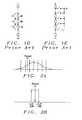
- FIG. 1Aa binary weighted trim DAC of prior art in which an analog signal (current) is created that starts with a current generator producing 84% of the required analog signal and selectable additional current to attain 100% of the value of the analog signal that is required. Selection is by digitally controlling switches, which allow the current from the additional circuits to be added to the current of the current generator producing 84% of the required current.
- FIG. 1Bis an approach of the prior art that is similar to that of FIG. 1A with the exception that each element of the selectable additional current has N elements of the minimum selectable current of the circuit of FIG. 1A.
- FIG. 1C of prior artis similar to FIG.
- FIG. 1Auses capacitance as the parameter that is being totalized to 100%.
- FIG. 1DAnother example of prior art is shown in FIG. 1D , where selectable elements of a voltage divider are used to create a voltage that is commensurate with the digital input. It should be noted that the values of the switchable elements are double the previous element, e.g. 1, 2, 4, 8, etc.
- FIG.1Eis a resistor voltage divider stack where each resistor is of the same value and a series of switches between each resistor is used to select the desired voltage.
- the circuits of FIG. 1A through 1Eform a DAC as a digital control in generating an analog value.
- US 2006/0274594(Huckaby et al. ) is directed to a method and apparatus for adjusting trim settings for internally generated voltages comparing a target digital value to a present digital value to introduce a trim value.
- US 2003/0197643 A1(Otani et al. ) is directed to a code in which resistor selection produces an output voltage that represents an input voltage.
- a circuitis directed to trimming reference voltages where the reference voltages are compared to an external comparison voltage.
- US 7,193,548 B2(Kaplan ) is directed to a digital-to-analog converter mismatch shaper using a delta sigma modulator that has analog signal processing components.
- a voltage and a current reference generatorare directed to a control stage couple to the reference generator stage to adjust trimmable parameters.
- US 7,642,852 B2(Chandra et al. ), is directed to a method and apparatus for trimming values of load resistors to reduce variation in a common mode feedback loop of an operational amplifier.
- US 7,433,790(Anderson et al. ) is directed to trimming of a reference controlled by an algorithm executed by logic circuitry.
- US 7,411,380 B2(Chang et al. ) is directed to a non-linear compensation circuit for compensating non-linear effects of a voltage reference.
- US 7,362,247 B2(Arias et al. ) is directed to digital correction of a multi-bit ADAC non-linearities for error feedback.
- US 7,019,585 B1(Wilson et al. ) is directed to a voltage trim circuit using an operational amplifier, a transistor, a voltage divider and a bias current circuit.
- a system and methodis directed to calibrating a digital-to-analog converter comprising a memory and logic circuitry for performing arithmetic operations.
- US 6,909,642 B2(Lehmann et al. )is directed to integrated circuit chips capable and the method thereof for self-adjusting the internal voltage the integrated circuit chip.
- US 6,906,581 B2(Kang et al. ) is directed to a fast start low-voltage bandgap voltage reference circuit using a first current generator with a positive temperature coefficient and second current generator with a negative temperature coefficient.
- IN US 6,897,794 B2(Kuyel et al. ) a system and method is directed to calibrating a digital-to analog converter that makes use of a resistor string.
- a circuitis directed to trimming the frequency of an oscillator.
- US 6,556,161 B2(Nuijten ) is direcdted to a multi-bit digital-to-analog converter comprising a plurality of conversion elements that are selected by dynamic element matching.
- US 6,329,804 B1(Mercer ) a method and apparatus is directed to trimming the level and slope in a voltage reference using a current switching DAC.
- US 6,157,245(Rincon-Mora ) is directed to a curvature corrected bandgap reference voltage circuit independent of temperature operation of the circuit.
- US 5,666,118(Gersbach ) is directed to a method of self-calibration for a segmented digital-to-analog converter comprising an output consisting of a voltage step and a trim value.
- a DACis trimmed to eliminate an error caused in the analog output by variations in the semiconductor process or minor defects that do not prevent the circuitry from working accurately.
- a trim circuit controlled by a state machine and comprising a T-DACis connected to the analog output of the DAC to measure the value of the analog output of the DAC with respect to a reference signal in order to control the T-DAC to adjust the value of the conversion of the digital signal to an analog value the output of the DAC to within plus or minus one half LSB of the digital input to the DAC.
- T-DACtrim DAC
- Contained within the state machineis a nonvolatile memory to store T-DAC settings for all combinations of the digital input to the DAC.
- the operation of the T-DACessentially forms a rectangular distribution of the analog output of the circuit that is one LSB wide at the analog target value required by the digital input to the DAC, wherein an undersized trim bit is used to help form a one bit wide distribution.
- the undersize value of a trim bitcan be different for each trim bit; therefore, creating a collection of undersize values.
- TABLE 1Shown in TABLE 1 is an example of reducing the factor (undersize fraction) by a small amount between the next more significant bit and the previous bit of the trim DAC.
- Thisforms a trim DAC with a strong negative DNL (differential non-linearity), which greatly reduces the probability that any major transition is greater than one LSB; and therefore, allowing the algorithm of the trim DAC to converge on a target distribution of one LSB.
- the major disadvantage of the approach shown in TABLE 1is that there is a reduction in the trim range.
- TABLE 2is shown an alternative to the undersizing in TABLE 1 where only the two most significant bits (most significant trim elements) are undersized by an undersize fraction, which addresses the DNL of the upper two major transitions (011111 to 100000 and x01111 to x10000).
- trim DACIn practice a trim DAC, as it is with other design elements, which require good matching, are designed in unit elements. Thus fractional ratios are generally not used. TABLE 3 demonstrates the use of unit ratios between the most significant bits. This is accomplished by reducing the unit ratio by one for the doubled value for each more significant bit. In TABLE 3 this reduction is shown for the three most significant bits of a six bit trim DAC. TABLE 3 MSB LSB Nominal 32 16 8 4 2 1 Real 27.0 15.0 7.0 4.0 2.0 1.0
- the approach demonstrated in the present inventionis applicable to any DAC application and is particularly applicable and useful in comparator based self-trim schemes. There are no restrictions on the trim algorithm, whether the search is linear, binary or left sided versus right sided. Further the approach demonstrated herein is applicable to a voltage DAC, a current DAC a frequency DAC or any other DAC that converts a set of digital signals into an analog output to control, condition or change an analog value or parameter.
- FIG. 2A of the present inventionis shown a natural distribution of the analog output of a DAC, which includes variations from device to device on a chip, chip to chip, wafer to wafer and batch to batch of the semiconductor product containing a DAC.
- the distributionis divided into one LSB sections with a target value demonstrating an example where the proper analog value could exist with respect to the distribution.
- FIG. 2Bdemonstrates the result of the present invention where the procedures of the present invention produced a rectangular distribution one LSB wide.
- the rectangular distribution of FIG. 2Brepresents the results of the trim DAC (T-DAC) to modify the natural distribution of FIG. 2A to form a T-DAC output that is plus or minus one half of a LSB around the target value.
- T-DACtrim DAC
- FIG. 3is shown a block diagram of the test circuit 30 of the present invention in which a state machine 31 controls a CUT (Circuit Under Trim) 32 comprising a T-DAC (trim DAC) 33.
- the CUTcan be a DAC having the capability to be digitally trimmed under the control of the state machine 31.
- the analog output of the CUTis connected to a comparator 34, which is compared to a reference provided by an automatic tester (ATE).
- ATEautomatic tester
- the output of the comparator 34is used to provide a digital signal to the T-DAC to correct the analog output signal to provide a value that is accurate within plus or minus one half of a LSB of a digital input value
- the trim algorithm within the state machine 31controls the T-DAC 33 to produce an analog output signal that is equivalent to the digital trim data including any undersize fraction.
- the digital trim data required to produce an analog output for a digital inputis stored in a nonvolatile memory associated with the state machine 31, which is used to lookup the appropriate combination of bits and the T-DAC settings to be used to correct for manufacturing variations in order to produce an accurate analog output for each combination of digital input bits to the CUT 32.
- the undersize fractionas aforementioned, enhances the probability of finding an equivalent output for major digital transitions, for example 011111 to 100000, x01111 to x10000 and xx0111 to xx1000.
- the state machine 31controls the T-DAC 33 with trim data in an attempt to form a rectangular distribution of the analog output that is one LSB wide.
- the state machineperforms a search of the input bits of the T-DAC that finds a combination that produces the desired rectangular distribution. Depending upon the direction of the search the rectangular distribution will be on one side of the reference or the other.
- a reference signalis supplied by the ATE through a switch SW1 is initially combined with a voltage representing a negative one half LSB at the summing junction of the positive input to the comparator 34. This determines whether the T-DAC has produced a result that is beyond the left portion (less positive portion) of the rectangular distribution. Then switch SW2 is activated to add a voltage that represents a plus one and a half LSB to the summing junction. The one and one half LSB addition to the summing junction cancels out the negative one half LSB and sets the positive input to the comparator to a voltage equivalent of a plus one LSB and tests for the trimmed DAC results to be less than one LSB wide.
- FIG. 4is shown a distribution of the analog signal output (see FIG. 3 ) of the trim DAC circuit 30 of the present invention.
- the distributionhas a width of one LSB starting at the value of the tester reference.
- the right tail of the distributionrepresents failed product where the trim algorithm is unable to bring that portion of the product within the 1 LSB portion of the distribution to the right of the reference.
- analog output signalcan be current or any other measurable analog signal. Further the approach demonstrated herein can be used in the conversion of analog signals to digital signals.
Landscapes
- Physics & Mathematics (AREA)
- Nonlinear Science (AREA)
- Engineering & Computer Science (AREA)
- Theoretical Computer Science (AREA)
- Analogue/Digital Conversion (AREA)
- Semiconductor Integrated Circuits (AREA)
Abstract
Description
- This application is related to US patent application docket number DS08-005, serial number 12/455,530, filed on June 03, 2009 (European patent application
09 392 001.5 filed on May 18, 2009 - The present invention is related mixed-signal integrated circuits and in particular the trimming digital to analog converters comprising voltage, current, time and frequency.
- The trend in microelectronics is the continued creation of smaller and smaller devices, wherein as the devices become smaller, variations in the fringe of each shape of a device become a larger portion of the of the performance characteristics of the device and cause variations in the performance of a circuit dependent on the device. This is particularly important in circuits that convert from one signal domain to another where precision in the conversion is required such as digital to analog converters. The variation in the output signal compared to an ideal response is known as a differential non-linearity (DNL) of the converted output signal.
- There are several approaches to correcting for manufacturing process variations in the production of semiconductor circuits, which attempt to correct for variations producing analog values. In
FIG. 1A is shown a binary weighted trim DAC of prior art in which an analog signal (current) is created that starts with a current generator producing 84% of the required analog signal and selectable additional current to attain 100% of the value of the analog signal that is required. Selection is by digitally controlling switches, which allow the current from the additional circuits to be added to the current of the current generator producing 84% of the required current.FIG. 1B is an approach of the prior art that is similar to that ofFIG. 1A with the exception that each element of the selectable additional current has N elements of the minimum selectable current of the circuit ofFIG. 1A. FIG. 1C of prior art is similar toFIG. 1A , but uses capacitance as the parameter that is being totalized to 100%. Another example of prior art is shown inFIG. 1D , where selectable elements of a voltage divider are used to create a voltage that is commensurate with the digital input. It should be noted that the values of the switchable elements are double the previous element, e.g. 1, 2, 4, 8, etc. InFIG.1E is a resistor voltage divider stack where each resistor is of the same value and a series of switches between each resistor is used to select the desired voltage. In the general, the circuits ofFIG. 1A through 1E form a DAC as a digital control in generating an analog value. These methods can provide useful results with the potential drag on conversion time needed to determine values created at the time of calibration. US 2006/0274594 (Huckaby et al. ) is directed to a method and apparatus for adjusting trim settings for internally generated voltages comparing a target digital value to a present digital value to introduce a trim value.US 2003/0197643 A1 (Otani et al. ) is directed to a code in which resistor selection produces an output voltage that represents an input voltage. InUS 2001/0004126 A1 (Ohlhoff ), a circuit is directed to trimming reference voltages where the reference voltages are compared to an external comparison voltage.US 7,193,548 B2 (Kaplan ) is directed to a digital-to-analog converter mismatch shaper using a delta sigma modulator that has analog signal processing components. InUS 7,675,792 B2 (Bedeschi et al. ), a voltage and a current reference generator are directed to a control stage couple to the reference generator stage to adjust trimmable parameters.US 7,642,852 B2 (Chandra et al. ), is directed to a method and apparatus for trimming values of load resistors to reduce variation in a common mode feedback loop of an operational amplifier.US 7,433,790 (Anderson et al. ) is directed to trimming of a reference controlled by an algorithm executed by logic circuitry.US 7,411,380 B2 (Chang et al. ) is directed to a non-linear compensation circuit for compensating non-linear effects of a voltage reference.US 7,362,247 B2 (Arias et al. ) is directed to digital correction of a multi-bit ADAC non-linearities for error feedback.US 7,019,585 B1 (Wilson et al. ) is directed to a voltage trim circuit using an operational amplifier, a transistor, a voltage divider and a bias current circuit. InUS 7,002,496 B2 (Kuyel ) a system and method is directed to calibrating a digital-to-analog converter comprising a memory and logic circuitry for performing arithmetic operations.US 6,909,642 B2 (Lehmann et al. )is directed to integrated circuit chips capable and the method thereof for self-adjusting the internal voltage the integrated circuit chip.US 6,906,581 B2 (Kang et al. ) is directed to a fast start low-voltage bandgap voltage reference circuit using a first current generator with a positive temperature coefficient and second current generator with a negative temperature coefficient. INUS 6,897,794 B2 (Kuyel et al. ) a system and method is directed to calibrating a digital-to analog converter that makes use of a resistor string. InUS 6,671,221 B2 (Beer et al. ) a circuit is directed to trimming the frequency of an oscillator.US 6,556,161 B2 (Nuijten ) is direcdted to a multi-bit digital-to-analog converter comprising a plurality of conversion elements that are selected by dynamic element matching. InUS 6,329,804 B1 (Mercer ) a method and apparatus is directed to trimming the level and slope in a voltage reference using a current switching DAC.US 6,157,245 (Rincon-Mora ) is directed to a curvature corrected bandgap reference voltage circuit independent of temperature operation of the circuit.US 5,666,118 (Gersbach ) is directed to a method of self-calibration for a segmented digital-to-analog converter comprising an output consisting of a voltage step and a trim value.US 5,352,973 (Audy ) is directed to an output curvature correction for a bandgap reference circuit that exhibits a temperature dependent output. InDas, T. et al.; inventor identified, "Self-calibration of input-match in RF front-end circuitry" IEEE Transactions, vol52, no. 12, pp. 821-825, Dec 2005 is directed to a technique to ascertain an input match frequency of a circuit by using a built-in-self-test structure, determines the frequency interval that needs to be shifted and feeds back a digital word to correct the input mismatch.- It is an objective of the present invention to trim the output of a DAC to within one LSB, wherein a trimmed value is a product of the digital input bits times a factor two between bits minus an undersize fraction where the undersize fraction is between, but not including, zero and one.
- It is also an objective of the present invention wherein the conversions of all bits are undersized excluding the least significant bit.
- It is still an objective of the present invention wherein the conversions of the more significant bits are undersized.
- It is still further an objective of the present invention wherein the conversions of the least significant bits are oversized by a fraction between, but not including, zero and one.
- It is yet another objective of the present invention to detect outlier values and form a rectangular distribution between plus and minus one half of an LSB.
- In the present invention a DAC is trimmed to eliminate an error caused in the analog output by variations in the semiconductor process or minor defects that do not prevent the circuitry from working accurately. A trim circuit controlled by a state machine and comprising a T-DAC (trim DAC) is connected to the analog output of the DAC to measure the value of the analog output of the DAC with respect to a reference signal in order to control the T-DAC to adjust the value of the conversion of the digital signal to an analog value the output of the DAC to within plus or minus one half LSB of the digital input to the DAC. Contained within the state machine is a nonvolatile memory to store T-DAC settings for all combinations of the digital input to the DAC.
- The operation of the T-DAC essentially forms a rectangular distribution of the analog output of the circuit that is one LSB wide at the analog target value required by the digital input to the DAC, wherein an undersized trim bit is used to help form a one bit wide distribution. The undersize value of a trim bit can be different for each trim bit; therefore, creating a collection of undersize values. The mathematical description of the operation of N-bit T-DAC is as follows.


where typical values of an are 0.1 to 0.5 - Shown in TABLE 1 is an example of reducing the factor (undersize fraction) by a small amount between the next more significant bit and the previous bit of the trim DAC. In the case of TABLE 1 with all an=0.1 or a 5% reduction. This forms a trim DAC with a strong negative DNL (differential non-linearity), which greatly reduces the probability that any major transition is greater than one LSB; and therefore, allowing the algorithm of the trim DAC to converge on a target distribution of one LSB. The major disadvantage of the approach shown in TABLE 1 is that there is a reduction in the trim range.
TABLE 1 MSB LSB Nominal 32 16 8 4 2 1 Real 26.13 13.75 7.24 3.81 1.9 1.0 - In TABLE 2 is shown an alternative to the undersizing in TABLE 1 where only the two most significant bits (most significant trim elements) are undersized by an undersize fraction, which addresses the DNL of the upper two major transitions (011111 to 100000 and x01111 to x10000).
TABLE 2 MSB LSB Nominal 32 16 8 4 2 1 Real 28.88 15.2 8.0 4.0 2.0 1.0 - In practice a trim DAC, as it is with other design elements, which require good matching, are designed in unit elements. Thus fractional ratios are generally not used. TABLE 3 demonstrates the use of unit ratios between the most significant bits. This is accomplished by reducing the unit ratio by one for the doubled value for each more significant bit. In TABLE 3 this reduction is shown for the three most significant bits of a six bit trim DAC.
TABLE 3 MSB LSB Nominal 32 16 8 4 2 1 Real 27.0 15.0 7.0 4.0 2.0 1.0 - In the situation where the reduction in the trim range is not acceptable, an oversizing of the least significant bits would provide similar trim results, as shown in TABLE 4. This approach would result in the widening of the trim distribution, which could be as wide as the LSB.
TABLE 4 MSB LSB Nominal 32 16 8 4 2 1 Real 32.0 16.0 8.0 4.0 2.2 1.2 - The approach demonstrated in the present invention is applicable to any DAC application and is particularly applicable and useful in comparator based self-trim schemes. There are no restrictions on the trim algorithm, whether the search is linear, binary or left sided versus right sided. Further the approach demonstrated herein is applicable to a voltage DAC, a current DAC a frequency DAC or any other DAC that converts a set of digital signals into an analog output to control, condition or change an analog value or parameter.
- This invention will be described with reference to the accompanying drawings, wherein:
FIG. 1A to1 E are trim approaches of prior art;FIG. 2A is a distribution of an untrimmed analog output value, as manufactured and separated into 1LSB units;FIG. 2B is a rectangular distribution of a trimmed output of a DAC of the present invention;FIG. 3 is a block diagram of the trim circuit of the present invention; andFIG. 4 is a rectangular trim distribution of the present invention that is modified by the DNL of the trim DAC.- In
FIG. 2A of the present invention is shown a natural distribution of the analog output of a DAC, which includes variations from device to device on a chip, chip to chip, wafer to wafer and batch to batch of the semiconductor product containing a DAC. The distribution is divided into one LSB sections with a target value demonstrating an example where the proper analog value could exist with respect to the distribution.FIG. 2B demonstrates the result of the present invention where the procedures of the present invention produced a rectangular distribution one LSB wide. The rectangular distribution ofFIG. 2B represents the results of the trim DAC (T-DAC) to modify the natural distribution ofFIG. 2A to form a T-DAC output that is plus or minus one half of a LSB around the target value. - In
FIG. 3 is shown a block diagram of thetest circuit 30 of the present invention in which astate machine 31 controls a CUT (Circuit Under Trim) 32 comprising a T-DAC (trim DAC) 33. The CUT can be a DAC having the capability to be digitally trimmed under the control of thestate machine 31. The analog output of the CUT is connected to acomparator 34, which is compared to a reference provided by an automatic tester (ATE). The output of thecomparator 34 is used to provide a digital signal to the T-DAC to correct the analog output signal to provide a value that is accurate within plus or minus one half of a LSB of a digital input value - The trim algorithm within the
state machine 31 controls the T-DAC 33 to produce an analog output signal that is equivalent to the digital trim data including any undersize fraction. The digital trim data required to produce an analog output for a digital input is stored in a nonvolatile memory associated with thestate machine 31, which is used to lookup the appropriate combination of bits and the T-DAC settings to be used to correct for manufacturing variations in order to produce an accurate analog output for each combination of digital input bits to theCUT 32. The undersize fraction, as aforementioned, enhances the probability of finding an equivalent output for major digital transitions, for example 011111 to 100000, x01111 to x10000 and xx0111 to xx1000. - The
state machine 31 controls the T-DAC 33 with trim data in an attempt to form a rectangular distribution of the analog output that is one LSB wide. The state machine performs a search of the input bits of the T-DAC that finds a combination that produces the desired rectangular distribution. Depending upon the direction of the search the rectangular distribution will be on one side of the reference or the other. - A reference signal is supplied by the ATE through a switch SW1 is initially combined with a voltage representing a negative one half LSB at the summing junction of the positive input to the
comparator 34. This determines whether the T-DAC has produced a result that is beyond the left portion (less positive portion) of the rectangular distribution. Then switch SW2 is activated to add a voltage that represents a plus one and a half LSB to the summing junction. The one and one half LSB addition to the summing junction cancels out the negative one half LSB and sets the positive input to the comparator to a voltage equivalent of a plus one LSB and tests for the trimmed DAC results to be less than one LSB wide. - In
FIG. 4 is shown a distribution of the analog signal output (seeFIG. 3 ) of thetrim DAC circuit 30 of the present invention. The distribution has a width of one LSB starting at the value of the tester reference. On both sides of the main part of the distribution, which is one LSB wide, are tails of the distribution where the trim algorithm will shape the distribution and where the comparator based trim eliminates the left tail before the reference. The right tail of the distribution represents failed product where the trim algorithm is unable to bring that portion of the product within the 1 LSB portion of the distribution to the right of the reference. - Whereas the example discussed herein is a circuit under test is a DAC with a voltage output, it should be noted that the analog output signal can be current or any other measurable analog signal. Further the approach demonstrated herein can be used in the conversion of analog signals to digital signals.
- While the invention has been particularly shown and described with reference to preferred embodiments thereof, it will be understood by those skilled in the art that various changes in form and details may be made without departing from the spirit and scope of the invention.


Claims (13)
- A method of trimming an analog value using a trim DAC, comprising:a) measuring an analog output of a trim DAC; andb) forming an nth bit, wherein an undersize factor of an analog equivalence between the nth bit and an n-1 bit of the trim DAC narrows a distribution of a value of said analog output.
- The method of claim 1, wherein said undersize factor is less than one and greater than zero.
- The method of claim 1, wherein said undersize factor between bits is applied to bits between a most significant bit and a second least significant bit of the digital input of said trim DAC.
- The method of claim 1, wherein said undersize factor between bits is applied to a first M most significant bits.
- The method of claim 1, wherein said undersize factor between bits is replaced with an oversize of a last L least significant bits.
- A trim DAC, comprising:a) a first binary trim bit;b) a second binary trim bit, wherein said second binary trim bit forms a next more significant binary trim bit to said first binary trim bit;c) said next more significant binary trim bit an undersized fraction of a normal difference factor between logically adjacent binary bits; andd) said undersize fraction reduces the probability of a major transition greater than a least significant bit.
- The trim DAC of claim 6, wherein said undersize fraction is a fraction (less than one and greater than zero) of the normal difference factor between logically adjacent binary bits.
- The trim DAC of claim 6, wherein said undersize fraction is applied to all binary trim bits except a least significant binary trim bit.
- The trim DAC of claim 6, wherein said undersize fraction is applied to most significant trim bits.
- The trim DAC of claim 9, wherein the most significant trim bits are a most significant trim bit and a next most significant trim bit.
- The trim DAC of claim 6, wherein said undersize fraction is applied in a unit value of the least significant bit and applied to more significant trim bits higher in significance than a second least significant trim bit.
- The trim DAC of claim 6, wherein said first binary trim bit is a least significant bit and said second binary trim bit is a next least significant bit, wherein an oversize factor is applied to the first and second binary trim bits.
- The trim DAC of claim 12, wherein the oversize factor maintains a range of the trim DAC at an expense of a wider trim distribution.
Priority Applications (2)
| Application Number | Priority Date | Filing Date | Title |
|---|---|---|---|
| EP11392001.1AEP2487797B1 (en) | 2011-02-11 | 2011-02-11 | Minimum differential non-linearity trim DAC |
| US12/932,376US8421659B2 (en) | 2011-02-11 | 2011-02-24 | Minimum differential non-linearity trim DAC |
Applications Claiming Priority (1)
| Application Number | Priority Date | Filing Date | Title |
|---|---|---|---|
| EP11392001.1AEP2487797B1 (en) | 2011-02-11 | 2011-02-11 | Minimum differential non-linearity trim DAC |
Publications (2)
| Publication Number | Publication Date |
|---|---|
| EP2487797A1true EP2487797A1 (en) | 2012-08-15 |
| EP2487797B1 EP2487797B1 (en) | 2014-04-09 |
Family
ID=44118497
Family Applications (1)
| Application Number | Title | Priority Date | Filing Date |
|---|---|---|---|
| EP11392001.1AActiveEP2487797B1 (en) | 2011-02-11 | 2011-02-11 | Minimum differential non-linearity trim DAC |
Country Status (2)
| Country | Link |
|---|---|
| US (1) | US8421659B2 (en) |
| EP (1) | EP2487797B1 (en) |
Families Citing this family (8)
| Publication number | Priority date | Publication date | Assignee | Title |
|---|---|---|---|---|
| JP2012151561A (en)* | 2011-01-17 | 2012-08-09 | Seiko Epson Corp | A/d conversion circuit, integrated circuit device and electronic apparatus |
| JP6036311B2 (en)* | 2013-01-09 | 2016-11-30 | 株式会社ソシオネクスト | Analog-digital conversion circuit and analog-digital conversion method |
| EP2894944A1 (en)* | 2014-01-14 | 2015-07-15 | Dialog Semiconductor GmbH | Method for improving the accuracy of an exponential current digital-to-analog (IDAC) using a binary-weighted MSB |
| EP2894943B1 (en)* | 2014-01-14 | 2020-02-26 | Dialog Semiconductor (UK) Limited | An apparatus for improving the accuracy of an exponential current digital-to-analog (IDAC) using a binary-weighted MSB |
| US9991901B2 (en) | 2015-09-03 | 2018-06-05 | International Business Machines Corporation | Method of optimizing CMOS IDAC linearity performance using golden ratio |
| US9571115B1 (en)* | 2015-11-13 | 2017-02-14 | International Business Machines Corporation | Analog to digital converter with high precision offset calibrated integrating comparators |
| FR3089370B1 (en)* | 2018-11-29 | 2020-11-27 | Teledyne E2V Semiconductors Sas | Analog signal generation device |
| CN118566706B (en)* | 2024-04-29 | 2025-04-01 | 上海锐星微电子科技有限公司 | A digital chip trimming method based on improved Trim algorithm |
Citations (22)
| Publication number | Priority date | Publication date | Assignee | Title |
|---|---|---|---|---|
| US5352973A (en) | 1993-01-13 | 1994-10-04 | Analog Devices, Inc. | Temperature compensation bandgap voltage reference and method |
| US5666118A (en) | 1995-03-06 | 1997-09-09 | International Business Machines Corporation | Self calibration segmented digital-to-analog converter |
| US6157245A (en) | 1999-03-29 | 2000-12-05 | Texas Instruments Incorporated | Exact curvature-correcting method for bandgap circuits |
| US20010004126A1 (en) | 1999-12-14 | 2001-06-21 | Carsten Ohlhoff | Configuration for trimming reference voltages in semiconductor chips, in particular semiconductor memories |
| US6329804B1 (en) | 1999-10-13 | 2001-12-11 | National Semiconductor Corporation | Slope and level trim DAC for voltage reference |
| US6417794B1 (en)* | 1999-09-09 | 2002-07-09 | Cirrus Logic, Inc. | System and apparatus for digitally calibrating capacitors in an analog-to-digital converter using successive approximation |
| US6556161B2 (en) | 2000-04-04 | 2003-04-29 | Koninklijke Philips Electronics N.V. | Digital to analog converter employing dynamic element matching |
| US20030197643A1 (en) | 1998-03-23 | 2003-10-23 | Fullerton Larry W. | System and method for position determination by impulse radio |
| US6671221B2 (en) | 2001-05-23 | 2003-12-30 | Infineon Technologies Ag | Semiconductor chip with trimmable oscillator |
| US6897794B2 (en) | 2003-07-03 | 2005-05-24 | Texas Instruments Incorporated | All-analog calibration of sting-DAC linearity: application to high voltage processes |
| US6906581B2 (en) | 2002-04-30 | 2005-06-14 | Realtek Semiconductor Corp. | Fast start-up low-voltage bandgap voltage reference circuit |
| US6909642B2 (en) | 2003-03-14 | 2005-06-21 | Infineon Technologies North American Corp. | Self trimming voltage generator |
| US7002496B2 (en) | 2004-01-07 | 2006-02-21 | Texas Instruments Incorporated | All-digital calibration of string DAC linearity using area efficient PWL approximation: eliminating hardware search and digital division |
| US7019585B1 (en) | 2003-03-25 | 2006-03-28 | Cypress Semiconductor Corporation | Method and circuit for adjusting a reference voltage signal |
| US20060274594A1 (en) | 2005-06-01 | 2006-12-07 | Huckaby Jennifer F | Implementation of a fusing scheme to allow internal voltage trimming |
| US7193548B2 (en) | 2004-01-30 | 2007-03-20 | Hrl Laboratories, Llc | Switching arrangement and DAC mismatch shaper using the same |
| US7362247B2 (en) | 2005-05-06 | 2008-04-22 | Agere Systems Inc. | Digital correction of nonlinearity errors of multibit delta-sigma digital to analog converters |
| US7411380B2 (en) | 2006-07-21 | 2008-08-12 | Faraday Technology Corp. | Non-linearity compensation circuit and bandgap reference circuit using the same |
| US7433790B2 (en) | 2005-06-06 | 2008-10-07 | Standard Microsystems Corporation | Automatic reference voltage trimming technique |
| US7642852B2 (en) | 2008-04-25 | 2010-01-05 | Texas Instruments Incorporated | Resistor self-trim circuit for increased performance |
| US7675792B2 (en) | 2007-09-26 | 2010-03-09 | Intel Corporation | Generating reference currents compensated for process variation in non-volatile memories |
| EP2253966A1 (en)* | 2009-05-18 | 2010-11-24 | Dialog Semiconductor GmbH | Self-trim and self-test of on-chip values |
Family Cites Families (6)
| Publication number | Priority date | Publication date | Assignee | Title |
|---|---|---|---|---|
| US4272760A (en)* | 1979-04-10 | 1981-06-09 | Burr-Brown Research Corporation | Self-calibrating digital to analog conversion system and method |
| US6664909B1 (en)* | 2001-08-13 | 2003-12-16 | Impinj, Inc. | Method and apparatus for trimming high-resolution digital-to-analog converter |
| JP2003318264A (en) | 2002-04-19 | 2003-11-07 | Rohm Co Ltd | Semiconductor integrated circuit device with variable output characteristic |
| JP4076925B2 (en)* | 2003-08-12 | 2008-04-16 | ローム株式会社 | Voltage generation circuit |
| US7394225B2 (en) | 2004-06-09 | 2008-07-01 | International Components Corporation | Pseudo constant current multiple cell battery charger configured with a parallel topology |
| US7468686B2 (en)* | 2007-02-06 | 2008-12-23 | Linear Technology Corporation | Systems and methods for providing compact digitally controlled trim of multi-segment circuits |
- 2011
- 2011-02-11EPEP11392001.1Apatent/EP2487797B1/enactiveActive
- 2011-02-24USUS12/932,376patent/US8421659B2/enactiveActive
Patent Citations (22)
| Publication number | Priority date | Publication date | Assignee | Title |
|---|---|---|---|---|
| US5352973A (en) | 1993-01-13 | 1994-10-04 | Analog Devices, Inc. | Temperature compensation bandgap voltage reference and method |
| US5666118A (en) | 1995-03-06 | 1997-09-09 | International Business Machines Corporation | Self calibration segmented digital-to-analog converter |
| US20030197643A1 (en) | 1998-03-23 | 2003-10-23 | Fullerton Larry W. | System and method for position determination by impulse radio |
| US6157245A (en) | 1999-03-29 | 2000-12-05 | Texas Instruments Incorporated | Exact curvature-correcting method for bandgap circuits |
| US6417794B1 (en)* | 1999-09-09 | 2002-07-09 | Cirrus Logic, Inc. | System and apparatus for digitally calibrating capacitors in an analog-to-digital converter using successive approximation |
| US6329804B1 (en) | 1999-10-13 | 2001-12-11 | National Semiconductor Corporation | Slope and level trim DAC for voltage reference |
| US20010004126A1 (en) | 1999-12-14 | 2001-06-21 | Carsten Ohlhoff | Configuration for trimming reference voltages in semiconductor chips, in particular semiconductor memories |
| US6556161B2 (en) | 2000-04-04 | 2003-04-29 | Koninklijke Philips Electronics N.V. | Digital to analog converter employing dynamic element matching |
| US6671221B2 (en) | 2001-05-23 | 2003-12-30 | Infineon Technologies Ag | Semiconductor chip with trimmable oscillator |
| US6906581B2 (en) | 2002-04-30 | 2005-06-14 | Realtek Semiconductor Corp. | Fast start-up low-voltage bandgap voltage reference circuit |
| US6909642B2 (en) | 2003-03-14 | 2005-06-21 | Infineon Technologies North American Corp. | Self trimming voltage generator |
| US7019585B1 (en) | 2003-03-25 | 2006-03-28 | Cypress Semiconductor Corporation | Method and circuit for adjusting a reference voltage signal |
| US6897794B2 (en) | 2003-07-03 | 2005-05-24 | Texas Instruments Incorporated | All-analog calibration of sting-DAC linearity: application to high voltage processes |
| US7002496B2 (en) | 2004-01-07 | 2006-02-21 | Texas Instruments Incorporated | All-digital calibration of string DAC linearity using area efficient PWL approximation: eliminating hardware search and digital division |
| US7193548B2 (en) | 2004-01-30 | 2007-03-20 | Hrl Laboratories, Llc | Switching arrangement and DAC mismatch shaper using the same |
| US7362247B2 (en) | 2005-05-06 | 2008-04-22 | Agere Systems Inc. | Digital correction of nonlinearity errors of multibit delta-sigma digital to analog converters |
| US20060274594A1 (en) | 2005-06-01 | 2006-12-07 | Huckaby Jennifer F | Implementation of a fusing scheme to allow internal voltage trimming |
| US7433790B2 (en) | 2005-06-06 | 2008-10-07 | Standard Microsystems Corporation | Automatic reference voltage trimming technique |
| US7411380B2 (en) | 2006-07-21 | 2008-08-12 | Faraday Technology Corp. | Non-linearity compensation circuit and bandgap reference circuit using the same |
| US7675792B2 (en) | 2007-09-26 | 2010-03-09 | Intel Corporation | Generating reference currents compensated for process variation in non-volatile memories |
| US7642852B2 (en) | 2008-04-25 | 2010-01-05 | Texas Instruments Incorporated | Resistor self-trim circuit for increased performance |
| EP2253966A1 (en)* | 2009-05-18 | 2010-11-24 | Dialog Semiconductor GmbH | Self-trim and self-test of on-chip values |
Non-Patent Citations (1)
| Title |
|---|
| DAS, T. ET AL.: "Self-calibration of input- match in RF front-end circuitry", IEEE TRANSACTIONS, vol. 52, no. 12, December 2005 (2005-12-01), pages 821 - 825 |
Also Published As
| Publication number | Publication date |
|---|---|
| US20120206283A1 (en) | 2012-08-16 |
| US8421659B2 (en) | 2013-04-16 |
| EP2487797B1 (en) | 2014-04-09 |
Similar Documents
| Publication | Publication Date | Title |
|---|---|---|
| EP2487797B1 (en) | Minimum differential non-linearity trim DAC | |
| US7978110B2 (en) | Digital-to-analog converter | |
| US9106246B2 (en) | Successive approximation register analog-to-digital converter and associated control method | |
| US8102204B2 (en) | Amplifiers with input offset trim and methods | |
| US7026967B2 (en) | Method for calibrating a digital-to-analog converter and a digital-to-analog converter | |
| US5861829A (en) | High-speed, low power, medium resolution analog-to-digital converter and method of stabilization | |
| US8049654B2 (en) | Digital trimming of SAR ADCs | |
| US9276598B1 (en) | Trim-matched segmented digital-to-analog converter apparatus, systems and methods | |
| EP1792402B1 (en) | Digital-to-analog converter structures | |
| EP3624345B1 (en) | Digital-to-analog converter transfer function modification | |
| US6118398A (en) | Digital-to-analog converter including current sources operable in a predetermined sequence and associated methods | |
| US5617091A (en) | Resistance ladder, D-A converter, and A-D converter | |
| US7394414B2 (en) | Error reduction in a digital-to-analog (DAC) converter | |
| CN114650061B (en) | Integrated circuit, digital-to-analog converter and driving method thereof | |
| EP1691247B1 (en) | Voltage supply interface with improved current sensitivity and reduced series resistance | |
| US7256721B2 (en) | Network with multiple adjustment elements and sensitivities, and digital-to-analog converter implementing same | |
| US11057042B2 (en) | Digital to analog converter device and calibration method | |
| US7145493B2 (en) | Digital-to-analog converter (DAC) circuits using different currents for calibration biasing and methods of operating same | |
| US6642867B1 (en) | Replica compensated heterogeneous DACs and methods | |
| US7196649B2 (en) | Reprogrammable distributed reference ladder for analog-to-digital converters | |
| Pastre et al. | High-precision DAC based on a self-calibrated sub-binary radix converter | |
| US11936395B2 (en) | Digital-to-analog converter with digitally controlled trim | |
| KR100335864B1 (en) | Digital/analog converter and digital/analog converting method | |
| JP4472490B2 (en) | Semiconductor integrated circuit and trimming method thereof | |
| US7034735B1 (en) | Trim circuits and methodologies for data converters |
Legal Events
| Date | Code | Title | Description |
|---|---|---|---|
| PUAI | Public reference made under article 153(3) epc to a published international application that has entered the european phase | Free format text:ORIGINAL CODE: 0009012 | |
| AK | Designated contracting states | Kind code of ref document:A1 Designated state(s):AL AT BE BG CH CY CZ DE DK EE ES FI FR GB GR HR HU IE IS IT LI LT LU LV MC MK MT NL NO PL PT RO RS SE SI SK SM TR | |
| AX | Request for extension of the european patent | Extension state:BA ME | |
| 17P | Request for examination filed | Effective date:20130215 | |
| RIC1 | Information provided on ipc code assigned before grant | Ipc:H03M 1/74 20060101ALN20130815BHEP Ipc:H03M 1/06 20060101ALN20130815BHEP Ipc:H03M 1/10 20060101AFI20130815BHEP | |
| GRAP | Despatch of communication of intention to grant a patent | Free format text:ORIGINAL CODE: EPIDOSNIGR1 | |
| INTG | Intention to grant announced | Effective date:20131018 | |
| GRAS | Grant fee paid | Free format text:ORIGINAL CODE: EPIDOSNIGR3 | |
| GRAA | (expected) grant | Free format text:ORIGINAL CODE: 0009210 | |
| AK | Designated contracting states | Kind code of ref document:B1 Designated state(s):AL AT BE BG CH CY CZ DE DK EE ES FI FR GB GR HR HU IE IS IT LI LT LU LV MC MK MT NL NO PL PT RO RS SE SI SK SM TR | |
| REG | Reference to a national code | Ref country code:GB Ref legal event code:FG4D | |
| REG | Reference to a national code | Ref country code:CH Ref legal event code:EP Ref country code:AT Ref legal event code:REF Ref document number:661814 Country of ref document:AT Kind code of ref document:T Effective date:20140415 | |
| REG | Reference to a national code | Ref country code:IE Ref legal event code:FG4D | |
| REG | Reference to a national code | Ref country code:DE Ref legal event code:R096 Ref document number:602011006034 Country of ref document:DE Effective date:20140522 | |
| REG | Reference to a national code | Ref country code:AT Ref legal event code:MK05 Ref document number:661814 Country of ref document:AT Kind code of ref document:T Effective date:20140409 | |
| REG | Reference to a national code | Ref country code:NL Ref legal event code:VDEP Effective date:20140409 | |
| REG | Reference to a national code | Ref country code:LT Ref legal event code:MG4D | |
| PG25 | Lapsed in a contracting state [announced via postgrant information from national office to epo] | Ref country code:LT Free format text:LAPSE BECAUSE OF FAILURE TO SUBMIT A TRANSLATION OF THE DESCRIPTION OR TO PAY THE FEE WITHIN THE PRESCRIBED TIME-LIMIT Effective date:20140409 Ref country code:IS Free format text:LAPSE BECAUSE OF FAILURE TO SUBMIT A TRANSLATION OF THE DESCRIPTION OR TO PAY THE FEE WITHIN THE PRESCRIBED TIME-LIMIT Effective date:20140809 Ref country code:FI Free format text:LAPSE BECAUSE OF FAILURE TO SUBMIT A TRANSLATION OF THE DESCRIPTION OR TO PAY THE FEE WITHIN THE PRESCRIBED TIME-LIMIT Effective date:20140409 Ref country code:NO Free format text:LAPSE BECAUSE OF FAILURE TO SUBMIT A TRANSLATION OF THE DESCRIPTION OR TO PAY THE FEE WITHIN THE PRESCRIBED TIME-LIMIT Effective date:20140709 Ref country code:NL Free format text:LAPSE BECAUSE OF FAILURE TO SUBMIT A TRANSLATION OF THE DESCRIPTION OR TO PAY THE FEE WITHIN THE PRESCRIBED TIME-LIMIT Effective date:20140409 Ref country code:GR Free format text:LAPSE BECAUSE OF FAILURE TO SUBMIT A TRANSLATION OF THE DESCRIPTION OR TO PAY THE FEE WITHIN THE PRESCRIBED TIME-LIMIT Effective date:20140710 Ref country code:BG Free format text:LAPSE BECAUSE OF FAILURE TO SUBMIT A TRANSLATION OF THE DESCRIPTION OR TO PAY THE FEE WITHIN THE PRESCRIBED TIME-LIMIT Effective date:20140709 | |
| PG25 | Lapsed in a contracting state [announced via postgrant information from national office to epo] | Ref country code:LV Free format text:LAPSE BECAUSE OF FAILURE TO SUBMIT A TRANSLATION OF THE DESCRIPTION OR TO PAY THE FEE WITHIN THE PRESCRIBED TIME-LIMIT Effective date:20140409 Ref country code:AT Free format text:LAPSE BECAUSE OF FAILURE TO SUBMIT A TRANSLATION OF THE DESCRIPTION OR TO PAY THE FEE WITHIN THE PRESCRIBED TIME-LIMIT Effective date:20140409 Ref country code:HR Free format text:LAPSE BECAUSE OF FAILURE TO SUBMIT A TRANSLATION OF THE DESCRIPTION OR TO PAY THE FEE WITHIN THE PRESCRIBED TIME-LIMIT Effective date:20140409 Ref country code:RS Free format text:LAPSE BECAUSE OF FAILURE TO SUBMIT A TRANSLATION OF THE DESCRIPTION OR TO PAY THE FEE WITHIN THE PRESCRIBED TIME-LIMIT Effective date:20140409 Ref country code:SE Free format text:LAPSE BECAUSE OF FAILURE TO SUBMIT A TRANSLATION OF THE DESCRIPTION OR TO PAY THE FEE WITHIN THE PRESCRIBED TIME-LIMIT Effective date:20140409 Ref country code:ES Free format text:LAPSE BECAUSE OF FAILURE TO SUBMIT A TRANSLATION OF THE DESCRIPTION OR TO PAY THE FEE WITHIN THE PRESCRIBED TIME-LIMIT Effective date:20140409 Ref country code:PL Free format text:LAPSE BECAUSE OF FAILURE TO SUBMIT A TRANSLATION OF THE DESCRIPTION OR TO PAY THE FEE WITHIN THE PRESCRIBED TIME-LIMIT Effective date:20140409 | |
| PG25 | Lapsed in a contracting state [announced via postgrant information from national office to epo] | Ref country code:PT Free format text:LAPSE BECAUSE OF FAILURE TO SUBMIT A TRANSLATION OF THE DESCRIPTION OR TO PAY THE FEE WITHIN THE PRESCRIBED TIME-LIMIT Effective date:20140811 | |
| REG | Reference to a national code | Ref country code:DE Ref legal event code:R097 Ref document number:602011006034 Country of ref document:DE | |
| PG25 | Lapsed in a contracting state [announced via postgrant information from national office to epo] | Ref country code:SK Free format text:LAPSE BECAUSE OF FAILURE TO SUBMIT A TRANSLATION OF THE DESCRIPTION OR TO PAY THE FEE WITHIN THE PRESCRIBED TIME-LIMIT Effective date:20140409 Ref country code:RO Free format text:LAPSE BECAUSE OF FAILURE TO SUBMIT A TRANSLATION OF THE DESCRIPTION OR TO PAY THE FEE WITHIN THE PRESCRIBED TIME-LIMIT Effective date:20140409 Ref country code:EE Free format text:LAPSE BECAUSE OF FAILURE TO SUBMIT A TRANSLATION OF THE DESCRIPTION OR TO PAY THE FEE WITHIN THE PRESCRIBED TIME-LIMIT Effective date:20140409 Ref country code:BE Free format text:LAPSE BECAUSE OF FAILURE TO SUBMIT A TRANSLATION OF THE DESCRIPTION OR TO PAY THE FEE WITHIN THE PRESCRIBED TIME-LIMIT Effective date:20140409 Ref country code:CZ Free format text:LAPSE BECAUSE OF FAILURE TO SUBMIT A TRANSLATION OF THE DESCRIPTION OR TO PAY THE FEE WITHIN THE PRESCRIBED TIME-LIMIT Effective date:20140409 Ref country code:DK Free format text:LAPSE BECAUSE OF FAILURE TO SUBMIT A TRANSLATION OF THE DESCRIPTION OR TO PAY THE FEE WITHIN THE PRESCRIBED TIME-LIMIT Effective date:20140409 | |
| PLBE | No opposition filed within time limit | Free format text:ORIGINAL CODE: 0009261 | |
| STAA | Information on the status of an ep patent application or granted ep patent | Free format text:STATUS: NO OPPOSITION FILED WITHIN TIME LIMIT | |
| 26N | No opposition filed | Effective date:20150112 | |
| PG25 | Lapsed in a contracting state [announced via postgrant information from national office to epo] | Ref country code:IT Free format text:LAPSE BECAUSE OF FAILURE TO SUBMIT A TRANSLATION OF THE DESCRIPTION OR TO PAY THE FEE WITHIN THE PRESCRIBED TIME-LIMIT Effective date:20140409 | |
| REG | Reference to a national code | Ref country code:DE Ref legal event code:R097 Ref document number:602011006034 Country of ref document:DE Effective date:20150112 | |
| PG25 | Lapsed in a contracting state [announced via postgrant information from national office to epo] | Ref country code:SI Free format text:LAPSE BECAUSE OF FAILURE TO SUBMIT A TRANSLATION OF THE DESCRIPTION OR TO PAY THE FEE WITHIN THE PRESCRIBED TIME-LIMIT Effective date:20140409 | |
| PG25 | Lapsed in a contracting state [announced via postgrant information from national office to epo] | Ref country code:LU Free format text:LAPSE BECAUSE OF FAILURE TO SUBMIT A TRANSLATION OF THE DESCRIPTION OR TO PAY THE FEE WITHIN THE PRESCRIBED TIME-LIMIT Effective date:20150211 | |
| REG | Reference to a national code | Ref country code:CH Ref legal event code:PL | |
| PG25 | Lapsed in a contracting state [announced via postgrant information from national office to epo] | Ref country code:LI Free format text:LAPSE BECAUSE OF NON-PAYMENT OF DUE FEES Effective date:20150228 Ref country code:MC Free format text:LAPSE BECAUSE OF FAILURE TO SUBMIT A TRANSLATION OF THE DESCRIPTION OR TO PAY THE FEE WITHIN THE PRESCRIBED TIME-LIMIT Effective date:20140409 Ref country code:CH Free format text:LAPSE BECAUSE OF NON-PAYMENT OF DUE FEES Effective date:20150228 | |
| REG | Reference to a national code | Ref country code:IE Ref legal event code:MM4A | |
| REG | Reference to a national code | Ref country code:FR Ref legal event code:ST Effective date:20151030 | |
| PG25 | Lapsed in a contracting state [announced via postgrant information from national office to epo] | Ref country code:IE Free format text:LAPSE BECAUSE OF NON-PAYMENT OF DUE FEES Effective date:20150211 | |
| PG25 | Lapsed in a contracting state [announced via postgrant information from national office to epo] | Ref country code:FR Free format text:LAPSE BECAUSE OF NON-PAYMENT OF DUE FEES Effective date:20150302 | |
| PG25 | Lapsed in a contracting state [announced via postgrant information from national office to epo] | Ref country code:MT Free format text:LAPSE BECAUSE OF FAILURE TO SUBMIT A TRANSLATION OF THE DESCRIPTION OR TO PAY THE FEE WITHIN THE PRESCRIBED TIME-LIMIT Effective date:20140409 | |
| PG25 | Lapsed in a contracting state [announced via postgrant information from national office to epo] | Ref country code:HU Free format text:LAPSE BECAUSE OF FAILURE TO SUBMIT A TRANSLATION OF THE DESCRIPTION OR TO PAY THE FEE WITHIN THE PRESCRIBED TIME-LIMIT; INVALID AB INITIO Effective date:20110211 Ref country code:SM Free format text:LAPSE BECAUSE OF FAILURE TO SUBMIT A TRANSLATION OF THE DESCRIPTION OR TO PAY THE FEE WITHIN THE PRESCRIBED TIME-LIMIT Effective date:20140409 | |
| PG25 | Lapsed in a contracting state [announced via postgrant information from national office to epo] | Ref country code:CY Free format text:LAPSE BECAUSE OF FAILURE TO SUBMIT A TRANSLATION OF THE DESCRIPTION OR TO PAY THE FEE WITHIN THE PRESCRIBED TIME-LIMIT Effective date:20140409 | |
| PG25 | Lapsed in a contracting state [announced via postgrant information from national office to epo] | Ref country code:TR Free format text:LAPSE BECAUSE OF FAILURE TO SUBMIT A TRANSLATION OF THE DESCRIPTION OR TO PAY THE FEE WITHIN THE PRESCRIBED TIME-LIMIT Effective date:20140409 | |
| PG25 | Lapsed in a contracting state [announced via postgrant information from national office to epo] | Ref country code:MK Free format text:LAPSE BECAUSE OF FAILURE TO SUBMIT A TRANSLATION OF THE DESCRIPTION OR TO PAY THE FEE WITHIN THE PRESCRIBED TIME-LIMIT Effective date:20140409 | |
| PG25 | Lapsed in a contracting state [announced via postgrant information from national office to epo] | Ref country code:AL Free format text:LAPSE BECAUSE OF FAILURE TO SUBMIT A TRANSLATION OF THE DESCRIPTION OR TO PAY THE FEE WITHIN THE PRESCRIBED TIME-LIMIT Effective date:20140409 | |
| PGFP | Annual fee paid to national office [announced via postgrant information from national office to epo] | Ref country code:DE Payment date:20250207 Year of fee payment:15 | |
| REG | Reference to a national code | Ref country code:DE Ref legal event code:R082 Ref document number:602011006034 Country of ref document:DE | |
| PGFP | Annual fee paid to national office [announced via postgrant information from national office to epo] | Ref country code:GB Payment date:20250130 Year of fee payment:15 |