EP2477212A1 - Polycrystalline silicon thin layers produced by titanium-supported metal-induced layer exchange - Google Patents
Polycrystalline silicon thin layers produced by titanium-supported metal-induced layer exchangeDownload PDFInfo
- Publication number
- EP2477212A1 EP2477212A1EP12152997AEP12152997AEP2477212A1EP 2477212 A1EP2477212 A1EP 2477212A1EP 12152997 AEP12152997 AEP 12152997AEP 12152997 AEP12152997 AEP 12152997AEP 2477212 A1EP2477212 A1EP 2477212A1
- Authority
- EP
- European Patent Office
- Prior art keywords
- layer
- titanium
- activator
- oxide
- metal
- Prior art date
- Legal status (The legal status is an assumption and is not a legal conclusion. Google has not performed a legal analysis and makes no representation as to the accuracy of the status listed.)
- Ceased
Links
- 229910052751metalInorganic materials0.000titleclaimsdescription15
- 239000002184metalSubstances0.000titleclaimsdescription15
- 229910021420polycrystalline siliconInorganic materials0.000titledescription5
- 238000000034methodMethods0.000claimsabstractdescription42
- 229910052782aluminiumInorganic materials0.000claimsabstractdescription14
- 229910052709silverInorganic materials0.000claimsabstractdescription9
- 239000000463materialSubstances0.000claimsabstractdescription8
- 239000000758substrateSubstances0.000claimsabstractdescription7
- OGIDPMRJRNCKJF-UHFFFAOYSA-Ntitanium oxideInorganic materials[Ti]=OOGIDPMRJRNCKJF-UHFFFAOYSA-N0.000claimsabstractdescription6
- GWEVSGVZZGPLCZ-UHFFFAOYSA-NTitan oxideChemical compoundO=[Ti]=OGWEVSGVZZGPLCZ-UHFFFAOYSA-N0.000claimsabstractdescription5
- 229910052710siliconInorganic materials0.000claimsabstractdescription5
- 229910052732germaniumInorganic materials0.000claimsabstractdescription3
- 239000012190activatorSubstances0.000claimsabstract7
- 238000010438heat treatmentMethods0.000claimsabstract3
- 229910052723transition metalInorganic materials0.000claimsabstract3
- 150000003624transition metalsChemical class0.000claimsabstract3
- 230000005855radiationEffects0.000claimsabstract2
- 238000004519manufacturing processMethods0.000claimsdescription2
- XAGFODPZIPBFFR-UHFFFAOYSA-NaluminiumChemical compound[Al]XAGFODPZIPBFFR-UHFFFAOYSA-N0.000abstractdescription13
- 239000004332silverSubstances0.000abstractdescription8
- 239000004065semiconductorSubstances0.000abstractdescription6
- 239000010703siliconSubstances0.000abstractdescription4
- GNPVGFCGXDBREM-UHFFFAOYSA-Ngermanium atomChemical compound[Ge]GNPVGFCGXDBREM-UHFFFAOYSA-N0.000abstractdescription3
- 230000003647oxidationEffects0.000abstract5
- 238000007254oxidation reactionMethods0.000abstract5
- 230000008569processEffects0.000description21
- 239000010936titaniumSubstances0.000description18
- RTAQQCXQSZGOHL-UHFFFAOYSA-NTitaniumChemical compound[Ti]RTAQQCXQSZGOHL-UHFFFAOYSA-N0.000description17
- LEVVHYCKPQWKOP-UHFFFAOYSA-N[Si].[Ge]Chemical compound[Si].[Ge]LEVVHYCKPQWKOP-UHFFFAOYSA-N0.000description17
- 229910052719titaniumInorganic materials0.000description16
- 239000011521glassSubstances0.000description10
- 229910000577Silicon-germaniumInorganic materials0.000description7
- BQCADISMDOOEFD-UHFFFAOYSA-NSilverChemical compound[Ag]BQCADISMDOOEFD-UHFFFAOYSA-N0.000description7
- 238000002425crystallisationMethods0.000description7
- 230000008025crystallizationEffects0.000description7
- 229910021417amorphous siliconInorganic materials0.000description6
- VEXZGXHMUGYJMC-UHFFFAOYSA-NHydrochloric acidChemical compoundClVEXZGXHMUGYJMC-UHFFFAOYSA-N0.000description4
- 230000005496eutecticsEffects0.000description4
- NDVLTYZPCACLMA-UHFFFAOYSA-Nsilver oxideChemical compound[O-2].[Ag+].[Ag+]NDVLTYZPCACLMA-UHFFFAOYSA-N0.000description4
- XUIMIQQOPSSXEZ-UHFFFAOYSA-NSiliconChemical compound[Si]XUIMIQQOPSSXEZ-UHFFFAOYSA-N0.000description3
- 230000015572biosynthetic processEffects0.000description3
- 239000010409thin filmSubstances0.000description3
- KRHYYFGTRYWZRS-UHFFFAOYSA-NFluoraneChemical compoundFKRHYYFGTRYWZRS-UHFFFAOYSA-N0.000description2
- 229910018530Si-AgInorganic materials0.000description2
- 229910008383Si—AgInorganic materials0.000description2
- -1aluminum-silicon-germaniumChemical compound0.000description2
- 230000008901benefitEffects0.000description2
- 229910021419crystalline siliconInorganic materials0.000description2
- 238000005566electron beam evaporationMethods0.000description2
- TWNQGVIAIRXVLR-UHFFFAOYSA-Noxo(oxoalumanyloxy)alumaneChemical compoundO=[Al]O[Al]=OTWNQGVIAIRXVLR-UHFFFAOYSA-N0.000description2
- 229910001923silver oxideInorganic materials0.000description2
- 239000007787solidSubstances0.000description2
- 238000004544sputter depositionMethods0.000description2
- 238000002207thermal evaporationMethods0.000description2
- 229910005703Ge—AgInorganic materials0.000description1
- 241000409201LuinaSpecies0.000description1
- 229910004298SiO 2Inorganic materials0.000description1
- 229910002796Si–AlInorganic materials0.000description1
- 229910008310Si—GeInorganic materials0.000description1
- SHSWOKVNBXWREX-UHFFFAOYSA-N[Ge].[Si].[Ag]Chemical compound[Ge].[Si].[Ag]SHSWOKVNBXWREX-UHFFFAOYSA-N0.000description1
- 230000004913activationEffects0.000description1
- 239000003570airSubstances0.000description1
- 229910045601alloyInorganic materials0.000description1
- 239000000956alloySubstances0.000description1
- PNEYBMLMFCGWSK-UHFFFAOYSA-Naluminium oxideInorganic materials[O-2].[O-2].[O-2].[Al+3].[Al+3]PNEYBMLMFCGWSK-UHFFFAOYSA-N0.000description1
- 239000012080ambient airSubstances0.000description1
- 238000000137annealingMethods0.000description1
- QVGXLLKOCUKJST-UHFFFAOYSA-Natomic oxygenChemical compound[O]QVGXLLKOCUKJST-UHFFFAOYSA-N0.000description1
- 230000004888barrier functionEffects0.000description1
- 230000002596correlated effectEffects0.000description1
- 238000000151depositionMethods0.000description1
- 238000005137deposition processMethods0.000description1
- 238000009792diffusion processMethods0.000description1
- 238000004070electrodepositionMethods0.000description1
- 238000005516engineering processMethods0.000description1
- 238000005530etchingMethods0.000description1
- 239000010408filmSubstances0.000description1
- 238000003780insertionMethods0.000description1
- 230000037431insertionEffects0.000description1
- 239000013080microcrystalline materialSubstances0.000description1
- 230000004048modificationEffects0.000description1
- 238000012986modificationMethods0.000description1
- 230000006911nucleationEffects0.000description1
- 238000010899nucleationMethods0.000description1
- 229910052760oxygenInorganic materials0.000description1
- 239000001301oxygenSubstances0.000description1
- 239000002244precipitateSubstances0.000description1
- 238000002360preparation methodMethods0.000description1
- 239000010453quartzSubstances0.000description1
- VYPSYNLAJGMNEJ-UHFFFAOYSA-Nsilicon dioxideInorganic materialsO=[Si]=OVYPSYNLAJGMNEJ-UHFFFAOYSA-N0.000description1
- 239000007790solid phaseSubstances0.000description1
- 239000000126substanceSubstances0.000description1
- 238000007740vapor depositionMethods0.000description1
Images


Classifications
- H—ELECTRICITY
- H01—ELECTRIC ELEMENTS
- H01L—SEMICONDUCTOR DEVICES NOT COVERED BY CLASS H10
- H01L21/00—Processes or apparatus adapted for the manufacture or treatment of semiconductor or solid state devices or of parts thereof
- H01L21/02—Manufacture or treatment of semiconductor devices or of parts thereof
- H01L21/02104—Forming layers
- H01L21/02365—Forming inorganic semiconducting materials on a substrate
- H01L21/02656—Special treatments
- H01L21/02664—Aftertreatments
- H01L21/02667—Crystallisation or recrystallisation of non-monocrystalline semiconductor materials, e.g. regrowth
- H01L21/02672—Crystallisation or recrystallisation of non-monocrystalline semiconductor materials, e.g. regrowth using crystallisation enhancing elements
- H—ELECTRICITY
- H01—ELECTRIC ELEMENTS
- H01L—SEMICONDUCTOR DEVICES NOT COVERED BY CLASS H10
- H01L21/00—Processes or apparatus adapted for the manufacture or treatment of semiconductor or solid state devices or of parts thereof
- H01L21/02—Manufacture or treatment of semiconductor devices or of parts thereof
- H01L21/04—Manufacture or treatment of semiconductor devices or of parts thereof the devices having potential barriers, e.g. a PN junction, depletion layer or carrier concentration layer
- H01L21/18—Manufacture or treatment of semiconductor devices or of parts thereof the devices having potential barriers, e.g. a PN junction, depletion layer or carrier concentration layer the devices having semiconductor bodies comprising elements of Group IV of the Periodic Table or AIIIBV compounds with or without impurities, e.g. doping materials
- H01L21/20—Deposition of semiconductor materials on a substrate, e.g. epitaxial growth solid phase epitaxy
- H—ELECTRICITY
- H01—ELECTRIC ELEMENTS
- H01L—SEMICONDUCTOR DEVICES NOT COVERED BY CLASS H10
- H01L21/00—Processes or apparatus adapted for the manufacture or treatment of semiconductor or solid state devices or of parts thereof
- H01L21/02—Manufacture or treatment of semiconductor devices or of parts thereof
- H01L21/02104—Forming layers
- H01L21/02365—Forming inorganic semiconducting materials on a substrate
- H01L21/02367—Substrates
- H01L21/0237—Materials
- H01L21/02425—Conductive materials, e.g. metallic silicides
- H—ELECTRICITY
- H01—ELECTRIC ELEMENTS
- H01L—SEMICONDUCTOR DEVICES NOT COVERED BY CLASS H10
- H01L21/00—Processes or apparatus adapted for the manufacture or treatment of semiconductor or solid state devices or of parts thereof
- H01L21/02—Manufacture or treatment of semiconductor devices or of parts thereof
- H01L21/02104—Forming layers
- H01L21/02365—Forming inorganic semiconducting materials on a substrate
- H01L21/02518—Deposited layers
- H01L21/02521—Materials
- H01L21/02524—Group 14 semiconducting materials
- H01L21/02532—Silicon, silicon germanium, germanium
- H—ELECTRICITY
- H01—ELECTRIC ELEMENTS
- H01L—SEMICONDUCTOR DEVICES NOT COVERED BY CLASS H10
- H01L21/00—Processes or apparatus adapted for the manufacture or treatment of semiconductor or solid state devices or of parts thereof
- H01L21/02—Manufacture or treatment of semiconductor devices or of parts thereof
- H01L21/04—Manufacture or treatment of semiconductor devices or of parts thereof the devices having potential barriers, e.g. a PN junction, depletion layer or carrier concentration layer
- H01L21/18—Manufacture or treatment of semiconductor devices or of parts thereof the devices having potential barriers, e.g. a PN junction, depletion layer or carrier concentration layer the devices having semiconductor bodies comprising elements of Group IV of the Periodic Table or AIIIBV compounds with or without impurities, e.g. doping materials
- H01L21/30—Treatment of semiconductor bodies using processes or apparatus not provided for in groups H01L21/20 - H01L21/26
- H01L21/324—Thermal treatment for modifying the properties of semiconductor bodies, e.g. annealing, sintering
Definitions
- SiGesilicon germanium
- inexpensive substratessuch as e.g. Glass
- TFTthin-film transistor
- the functionality of these componentsis determined primarily by the electrical properties of the semiconductive material. These properties are strongly correlated with the microscopic structure, distinguishing between amorphous, nanocrystalline, microcrystalline, polycrystalline and monocrystalline materials. In general, the quality of the devices with increasing crystallinity (amorphous -> crystalline) is improved. The switching times of amorphous TFT screens, for example, are longer than those of microcrystalline, the efficiencies of amorphous solar cells lower than that of polycrystalline.
- T ⁇ 600 ° Cglass-compatible low-temperature crystallization (T ⁇ 600 ° C) of amorphous silicon germanium are mainly the laser-induced crystallization (laser-induced crystallization), LIC) and the metal-induced Crystallization (metal-induced crystallization, MIC) scientifically investigated or used industrially.
- Solid Phase Crystallization (SPC)requires temperatures greater than 600 ° C and is not compatible with the use of conventional glass substrates.
- MICis a true low-temperature process (T ⁇ 600 ° C) [Her72].
- the crystallization of amorphous semiconductorshas been observed in metal / semiconductor layer systems as well as in metal-doped amorphous layers [Rad91], [Cha01].
- the silver-induced layer exchange (Agile) processshowed that reproducibility is a major problem. This is probably due to the very unstable silver oxide layer, which is a diffusion barrier in the process and is essential for layer exchange.
Landscapes
- Engineering & Computer Science (AREA)
- Manufacturing & Machinery (AREA)
- Microelectronics & Electronic Packaging (AREA)
- Physics & Mathematics (AREA)
- Condensed Matter Physics & Semiconductors (AREA)
- General Physics & Mathematics (AREA)
- Power Engineering (AREA)
- Computer Hardware Design (AREA)
- Chemical & Material Sciences (AREA)
- Crystallography & Structural Chemistry (AREA)
- Materials Engineering (AREA)
- Recrystallisation Techniques (AREA)
- Photovoltaic Devices (AREA)
- Thin Film Transistor (AREA)
- Electrodes Of Semiconductors (AREA)
Abstract
Description
Translated fromGermanDie Herstellung von kristallinen Silizium-Germanium (SiGe) Dünnschichten auf kostengünstigen Substraten wie z.B. Glas ist von fundamentaler Bedeutung für großflächige elektronische Bauelemente. Hierzu zählen beispielsweise Dünnschicht-Solarzellen und Bildschirme, die auf Basis der Dünnschicht-Transistor-Technologie (TFT-Technologie) beruhen.The preparation of crystalline silicon germanium (SiGe) thin films on inexpensive substrates such as e.g. Glass is of fundamental importance for large-area electronic components. These include, for example, thin-film solar cells and screens based on thin-film transistor (TFT) technology.
Die Funktionsfähigkeit dieser Bauelemente wird in erster Linie durch die elektrischen Eigenschaften des halbleitenden Materials bestimmt. Diese Eigenschaften sind stark mit der mikroskopischen Struktur korreliert, wobei man zwischen amorphen, nanokristallinen, mikrokristallinen, polykristallinen und einkristallinen Materialien unterscheidet. Im Allgemeinen wird die Qualität der Bauelemente mit zunehmender Kristallinität (amorph -> kristallin) verbessert. Die Schaltzeiten von amorphen TFT-Bildschirmen sind beispielsweise länger als die von mikrokristallinen, die Wirkungsgrade von amorphen Solarzellen geringer als die von polykristallinen.The functionality of these components is determined primarily by the electrical properties of the semiconductive material. These properties are strongly correlated with the microscopic structure, distinguishing between amorphous, nanocrystalline, microcrystalline, polycrystalline and monocrystalline materials. In general, the quality of the devices with increasing crystallinity (amorphous -> crystalline) is improved. The switching times of amorphous TFT screens, for example, are longer than those of microcrystalline, the efficiencies of amorphous solar cells lower than that of polycrystalline.
Zur Glas-kompatiblen Niedertemperatur-Kristallisation (T < 600 °C) von amorphen Silizium-Germanium werden vor allem die Laser-induzierte Kristallisierung (Laser-induced Crystallization), LIC) und die Metall-induzierte Kristallisierung (Metal-induced Crystallization, MIC) wissenschaftlich untersucht bzw. industriell eingesetzt. Die Festphasen-Kristallisierung (Solid Phase Crystallization, SPC) erfordert Temperaturen größer als 600 °C und ist nicht kompatibel mit der Verwendung von konventionellen Glas-Substraten.For glass-compatible low-temperature crystallization (T <600 ° C) of amorphous silicon germanium are mainly the laser-induced crystallization (laser-induced crystallization), LIC) and the metal-induced Crystallization (metal-induced crystallization, MIC) scientifically investigated or used industrially. Solid Phase Crystallization (SPC) requires temperatures greater than 600 ° C and is not compatible with the use of conventional glass substrates.
Bei der LIC werden amorphe Halbleiterschichten durch intensives Laser-Licht kurzzeitig aufgeschmolzen (T = 1500 °C), so dass sich mikrokristallines Material mit Korngrößen von bis zu 5 µm bildete [Eis03]. Im Gegensatz dazu stellt die MIC ein echtes Niedertemperatur-Verfahren (T < 600 °C) dar [Her72]. Die Kristallisation von amorphen Halbleitern wurde sowohl in Metall/Halbleiter Schichtsystemen als auch in Metall-dotierten amorphen Schichten beobachtet [Rad91], [Cha01].In the LIC amorphous semiconductor layers are briefly melted by intense laser light (T = 1500 ° C), so that microcrystalline material with grain sizes of up to 5 microns formed [Eis03]. In contrast, MIC is a true low-temperature process (T <600 ° C) [Her72]. The crystallization of amorphous semiconductors has been observed in metal / semiconductor layer systems as well as in metal-doped amorphous layers [Rad91], [Cha01].
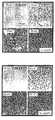
Ein viel versprechendes, großflächig anwendbares und zur Zeit intensiv erforschtes Verfahren stellt der Aluminium-induzierte Schichtaustausch (Aluminum-induced Layer Exchange, ALILE) von Silizium, Germanium bzw. Silizium-Germanium-Legierungen dar [Maj77], [Nas98], [Gju04]. Amorphes Silizium-Germanium wird dabei auf Aluminium-beschichtete Glassubstrate aufgebracht und unterhalb der eutektischen Temperatur des Aluminium-Silizium-Germanium-Systems (Te = 420 °C) getempert. Während des Temperns lösen sich Silizium- und Germanium-Atome aus der amorphen Schicht in der Aluminium-Schicht. Wenn die Sättigungsgrenze erreicht ist, fällen kristalline Si-Ge-Keime aus. Diese wachsen lateral und bilden am Ende eine geschlossene polykristalline Schicht, welche die gleiche Schichtdicke aufweist, wie die ursprüngliche Aluminium-Schicht. In
- a) Typisches Schichtsystem für den Aluminium-induzierten Schichtaustausch von Silizium-Germanium. Zwischen dem Aluminium (ca. 200 nm) und dem amorphen Silizium-Germanium (ca. 200 nm) befindet sich eine in der Skizze angedeutete dünne Aluminium-Oxid-Schicht. Wird diese Schichtstruktur bei Temperaturen unterhalb der eutektischen Temperatur des Aluminium-Silizium-Germanium-Systems (420 °C) getempert.a) Typical layer system for the aluminum-induced layer replacement of silicon germanium. Between the aluminum (about 200 nm) and the amorphous silicon germanium (about 200 nm) is a thin aluminum oxide layer indicated in the sketch. If this layer structure at temperatures below the eutectic temperature of the aluminum-silicon-germanium system (420 ° C) annealed.
- b) Es bilden sich an der Grenzfläche zwischen dem Aluminium und der amorphen SiGe-Schicht kristalline Silizium-Germanium-Keime aus, die in die Aluminium-Schicht hineinwachsen.b) Form at the interface between the aluminum and the amorphous SiGe layer crystalline silicon germanium nuclei, which grow into the aluminum layer.
- c) Das vertikale Wachstum wird durch die Substratoberfläche begrenzt. Anschließend findet laterales Wachstum der Kristallite bis zur Bildung einer geschlossenen polykristallinen Silizium-Germanium-Schicht statt.c) The vertical growth is limited by the substrate surface. Subsequently, lateral growth of the crystallites takes place until the formation of a closed polycrystalline silicon-germanium layer.
- d) Das sich nach dem Prozess an der Oberfläche befindende Aluminium kann durch nasschemische Verfahren entfernt werden (z.B. Ätzen in Salzsäure). Zurück bleibt eine polykristalline Silizium-Germanium-Schicht auf Glas mit lateralen Kristallitgrößen bis zu 50 µm.d) The aluminum present on the surface after the process can be removed by wet-chemical methods (for example, etching in hydrochloric acid). What remains is a polycrystalline silicon germanium layer on glass with lateral crystallite sizes of up to 50 μm.
Dieser Prozess konnte in unserer Gruppe auf das Materialsystem: Silber Silizium-Germanium erweitert werden. Der Prozess verläuft makroskopisch analog zum ALILE-Prozess [Gju05].In our group this process could be extended to the material system: silver silicon germanium. The process is macroscopically analogous to the ALILE process [Gju05].
Beim ALILE-Prozess mit Aluminiumoxid an der Grenzfläche ist für das Erlangen einer großkörnigen polykristallinen Schicht (Korngrößen > 20 µm) eine niedrige Prozesstemperatur (typischerweise unter 500 °C) nötig. Dies führt aber zu sehr langsamen Prozessen, die mehrere Stunden dauern können.In the ALILE process with alumina at the interface, a low process temperature (typically below 500 ° C) is required to obtain a large-grained polycrystalline layer (grain sizes> 20 μm). However, this leads to very slow processes that can take several hours.
Beim Silber-induzierten Schichtaustausch (AgILE) Prozess zeigte sich, dass die Reproduzierbarkeit ein großes Problem darstellt. Dies liegt wahrscheinlich an der sehr instabilen Silberoxidschicht, die bei dem Prozess eine Diffusionsbarriere darstellt und für den Schichtaustausch essentiell ist.The silver-induced layer exchange (Agile) process showed that reproducibility is a major problem. This is probably due to the very unstable silver oxide layer, which is a diffusion barrier in the process and is essential for layer exchange.
Beim AgILE Prozess ist im Gegensatz zum ALILE Prozess ein Schichtaustausch in umgekehrter Schichtfolge (Si/SiO2/Silber) nicht möglich. Diese Schichtfolge würde sich aber für die Solarzellenproduktion anbieten, da man bei diesem Prozess einen sehr gut reflektierenden Silberrückkontakt unterhalb der polykristallinen Halbleiterschicht erhalten würde.In contrast to the ALILE process, in the Agile process it is not possible to exchange layers in the reverse sequence (Si / SiO2 / silver). However, this layer sequence would offer itself for solar cell production, since in this process a very well reflecting silver back contact would be obtained below the polycrystalline semiconductor layer.
Der von uns entwickelte und bisher in der Literatur noch nicht beschriebene Titan-unterstützte Metall induzierte Schichtaustausch (Titan-assisted metal-induced layer exchange, Ti.MILE) löst die oben genannten Probleme wie folgt:
- a) durch das Aufbringen einer Titan-Zwischenschicht und das dadurch erfolgte Ersetzen der Aluminiumoxid- bzw. Silberoxidschicht durch eine Titanoxidschicht lässt sich beim ALILE-Prozess die Keimbildungsenergie gegenüber dem konventionellen Prozess deutlich erhöhen. Dies führt sowohl beim ALILE- als auch beim AgILE-Prozess zu deutlich größeren Kristalliten, wobei die Prozessdauer in der gleichen Größenordnung verbleibt.
- b) durch das Einfügen einer Titan-Zwischenschicht wird der umgekehrte Silberinduzierte Schichtaustausch ermöglicht.
- a) by the application of a titanium intermediate layer and the resulting replacement of the aluminum oxide or silver oxide layer by a titanium oxide layer can be significantly increase the nucleation energy over the conventional process in the ALILE process. This results in significantly larger crystallites in both the ALILE and Agile processes, with the process duration remaining the same order of magnitude.
- b) by the insertion of a titanium intermediate layer, the reverse silver-induced layer exchange is made possible.
- Auf ein amorphes oder kristallines Substrat (z.B. Glas, Quarz, Silizium-Wafer) wird eine 20-600 nm (typischerweise 200 nm) dicke Aluminium bzw. SilberSchicht mit einem geeigneten Verfahren aufgebracht (z.B. thermisches Verdampfen, Elektronenstrahl-Verdampfen, Sputtern, elektrochemisches Aufbringen des Metalls, etc.). Auf diese wird eine dünne Titanschicht (typischerweise 2-10 nm) aufgebracht.On an amorphous or crystalline substrate (eg, glass, quartz, silicon wafer), a 20-600 nm (typically 200 nm) thick aluminum or silver layer is applied by a suitable method (eg thermal evaporation, electron beam evaporation, sputtering, electrochemical deposition of the metal, etc.). A thin layer of titanium (typically 2-10 nm) is applied to this.
- Nach diesem Depositions-Prozess wird das Titan für kurze Zeit (einige Minuten) der Umgebungsluft ausgesetzt. Dieser Schritt ist nicht zwingend notwendig, verbessert aber die Oberflächenstruktur der resultierenden polykristallinen Halbleiter-Schicht.After this deposition process, the titanium is exposed to ambient air for a short time (a few minutes). This step is not essential, but improves the surface structure of the resulting polycrystalline semiconductor layer.
- Auf das Metall-Titan Schichtsystem wird nun eine Silizium-Germanium-Schicht mit einem geeigneten Verfahren aufgebracht (z.B. thermisches Verdampfen, Elektronenstrahl-Verdampfen, Sputtern, Gasphasenabscheidung, etc.). Die Dicke dieser Schicht sollte vergleichbar mit der Dicke der Metall-Schicht sein.A silicon-germanium layer is then applied to the metal-titanium layer system by a suitable method (e.g., thermal evaporation, electron beam evaporation, sputtering, vapor deposition, etc.). The thickness of this layer should be comparable to the thickness of the metal layer.
- Die so gewonnene Probenstruktur wird unterhalb der eutektischen Temperaturen des jeweiligen Materialsystems getempert (z.B. Si-Al 570 °C; Si-Ag 830 °C, ...), bis sich die Schichtfolge spontan austauscht. Abhängig von der verwendeten Temperatur dauert dieser Prozess zwischen einigen Sekunden bis hin zu einigen zehn Stunden. Die ursprüngliche Schichtstruktur Glas/Metall/ Titan/amorphes Silizium-Germanium wird dabei in eine Glas/polykristallines Silizium-Germanium/Titan/Metall Struktur umgewandelt.The sample structure obtained in this way is tempered below the eutectic temperatures of the respective material system (eg Si-Al 570 ° C., Si-Ag 830 ° C.,...) Until the sequence of layers spontaneously exchanges. Depending on the temperature used, this process takes between a few seconds to to some ten hours. The original layer structure glass / metal / titanium / amorphous silicon germanium is thereby converted into a glass / polycrystalline silicon germanium / titanium / metal structure.
- Das Aluminium kann nasschemisch, z.B. mit Salzsäure, von der getemperten Probe entfernt werden. Titan bzw. Titanoxid lässt sich z.B. nasschemisch mit Flußsäure entfernen. Als Ergebnis erhält man eine polykristalline Silizium-Germanium-Schicht auf Glas.The aluminum can be wet-chemically, e.g. with hydrochloric acid, are removed from the annealed sample. Titanium or titanium oxide can be e.g. Remove wet chemically with hydrofluoric acid. As a result, a polycrystalline silicon germanium layer is obtained on glass.
- Beim umgekehrten Silber-induzierten Schichtaustausch wird zuerst die Silizium-Germanium-Schicht mit einer der oben genannten Methoden deponiert.In the case of reverse silver-induced layer exchange, the silicon-germanium layer is first deposited using one of the abovementioned methods.
- Diese kann einige Zeit an Luft gelagert werden oder es kann direkt eine dünne (2-10 nm) dicke Titanschicht mit einer geeigneten Depositionsmethode aufgebracht werden (siehe a).This can be stored for some time in air or it can directly a thin (2-10 nm) thick titanium layer by a suitable deposition method are applied (see a).
- Diese Schichtfolge sollte für einige Minuten einer sauerstoffhaltigen Atmosphäre ausgesetzt werden, um die Bildung einer Titanoxidschicht zu ermöglichen. Dies ist nicht zwingend notwendig, verbessert aber die Qualität der Schichten.This layer sequence should be exposed to an oxygen-containing atmosphere for a few minutes to allow formation of a titanium oxide layer. This is not absolutely necessary, but improves the quality of the layers.
- Auf dieses Schichtsystem wird nun eine Silberschicht abgeschieden. Die Schichtdicke ist hierbei ähnlich der amorphen Silizium-Germanium-Schicht.On this layer system now a silver layer is deposited. The layer thickness is similar to the amorphous silicon germanium layer.
- Die so gewonnene Probenstruktur wird unterhalb der eutektischen Temperaturen des jeweiligen Materialsystems getempert (Si-Ag 830 °C; Ge-Ag 650 °C), bis sich die Schichtfolge spontan austauscht. Abhängig von der verwendeten Temperatur dauert dieser Prozess zwischen einigen Minuten bis hin zu einigen zehn Stunden. Die ursprüngliche Schichtstruktur Glas/amorphes Silizium-Germanium/Titan/Metall wird dabei in eine Glas/Metall/Titan/polykristallines Silizium-Germanium Struktur umgewandelt.The sample structure thus obtained is tempered below the eutectic temperatures of the respective material system (Si-Ag 830 ° C., Ge-Ag 650 ° C.) until the sequence of layers spontaneously exchanges. Depending on the temperature used, this process can take anywhere from a few minutes to a few tens of hours. The original layer structure glass / amorphous silicon germanium / titanium / metal is thereby converted into a glass / metal / titanium / polycrystalline silicon germanium structure.
Der Vorteil des hier beschriebenen Verfahrens lässt sich wie folgt zusammenfassen:
- Die dünne Zwischenschicht aus Titan erhöht die Aktivierungsenergie für die Bildung neuer Kristallite und führt so bei vergleichbaren Temperaturen zu deutlich größeren Kristalliten, ohne dabei aber den Gesamt-Prozess zu verlangsamen.
- The thin intermediate layer of titanium increases the activation energy for the formation of new crystallites and thus leads at comparable temperatures to significantly larger crystallites, but without slowing down the overall process.
Die Modifikation des bereits bekannten "Aluminium-induzierten Schichtaustauschs" durch das Einbringen einer zusätzlichen funktionalen Dünnschicht aus Titan, ist als das wesentlich Neue der Erfindung anzusehen.The modification of the already known "aluminum-induced layer exchange" by the introduction of an additional functional thin layer of titanium, is to be regarded as the essentially new of the invention.
- [ChaO1I][ChaO1I]
I. Chambouleyron, F. Fajardo, A.R. Zanatta, Appl. Phys. Lett. 79, 3233 (2001 I. Chambouleyron, F. Fajardo, AR Zanatta, Appl. Phys. Lett. 79, 3233 (2001 - [Eis03][Eis03]
C. Eisele, M. Berger, M. Nerding, H.P. Strunk, C.E. Nebel, M. Stutzmann, Thin Solid Films 427, 176 (2003 C. Eisele, M. Berger, M. Nerding, HP Strunk, CE Nebel, M. Stutzmann, Thin Solid Films 427, 176 (2003 - [Gju04][Gju04]
M. Gjukic, M. Buschbeck, R. Lechner, M. Stutzmann, Appl. Phys. Lett. 85, 2134 (2004 M. Gjukic, M. Buschbeck, R. Lechner, M. Stutzmann, Appl. Phys. Lett. 85, 2134 (2004 - [Gju05][Gju05]
M. Gjukic, M. Scholz, and M. Stutzmann, Erfindungsmeldung: Silber-induzierter Schichtaustausch (AgILE)M. Gjukic, M. Scholz, and M. Stutzmann, Invention Announcement: Silver-induced Layer Exchange (Agile) - [Her72][Her72]
S.R. Herd, P. Chaudhari, H.M. Brodsky, J. Cryst-Non Solids 7, 309 (1972 SR Herd, P. Chaudhari, HM Brodsky, J. Cryst-Non Solids 7, 309 (1972 - [Maj77][Maj77]
G. Majni, G. Ottaviani, Appl. Phys. Lett. 31, 125 (1977 G. Majni, G. Ottaviani, Appl. Phys. Lett. 31, 125 (1977 - [Nas98][Nas98]
O. Nast, T. Puzzer, L.M. Koschier, A.B. Sproul, R.S. Wenham, Appl. Phys. Lett. 73, 3214 (1998 O. Nast, T. Puzzer, LM Koschier, AB Sproul, RS Wenham, Appl. Phys. Lett. 73, 3214 (1998 - [Rad91][Rad91]
G. Radnoczi, A. Robertsson, H.T.G. Hentzell, S.F. Gong, M.-A. Hasan, J. Appl. Phys. 69 (1991) 6394G. Radnoczi, A. Robertsson, H.T.G. Hentzell, S.F. Gong, M.-A. Hasan, J. Appl. Phys. 69 (1991) 6394
Weitere Anlagen: Forschungsantrag zum Förderkennzeichen 0329986Further attachments: Research application for grant number 0329986
Claims (8)
Translated fromGermandadurch gekennzeichnet, dass die Oxidschicht auf der Basis eines Oxids eines Übergangsmetalls hergestellt wird, mit dem eine während der Wärmebehandlung stabile Oxidschicht erzeugbar ist.
characterized in that the oxide layer is made on the basis of an oxide of a transition metal with which a stable during the heat treatment oxide layer can be produced.
dadurch gekennzeichnet, dass die Oxidschicht auf einer zwischen Ausgangsschicht und Aktivatorschicht angeordneten metallischen Zwischenschicht ausgebildet wird.Method according to claim 2,
characterized in that the oxide layer is formed on a disposed between the starting layer and activator layer metallic intermediate layer.
dadurch gekennzeichnet, dass die Oxidschicht auf der Basis von Titanoxid ausgebildet wird.Method according to claim 1 or 2,
characterized in that the oxide layer is formed on the basis of titanium oxide.
dadurch gekennzeichnet, dass die Aktivatorschicht auf der Basis eines Metalls oder eines Übergangsmetalls hergestellt wird.Method according to one of claims 1 to 3,
characterized in that the activator layer is made on the basis of a metal or a transition metal.
dadurch gekennzeichnet, dass die Aktivatorschicht aus Al oder Ag hergestellt wird.Method according to claim 4,
characterized in that the activator layer is made of Al or Ag.
dadurch gekennzeichnet, dass die Ausgangsschicht aus wenigstens einem halbleitenden Material hergestellt wird.Method according to one of claims 1 to 5,
characterized in that the starting layer is made of at least one semiconductive material.
dadurch gekennzeichnet, dass die Ausgangsschicht wenigstens ein Element aus der Gruppe Si, Ge enthält.Method according to claim 6,
characterized in that the starting layer contains at least one element from the group Si, Ge.
dadurch gekennzeichnet, dass die Vorrichtung mithilfe eines Verfahrens nach einem der Ansprüche 1 bis 7 hergestellt ist.Device for converting radiation into electrical energy,
characterized in that the device is made by a method according to any one of claims 1 to 7.
Applications Claiming Priority (1)
| Application Number | Priority Date | Filing Date | Title |
|---|---|---|---|
| EP08157885.8AEP2133907B1 (en) | 2008-06-09 | 2008-06-09 | Polycrystalline silicon thin layers produced by titanium-supported metal-induced layer exchange |
Related Parent Applications (2)
| Application Number | Title | Priority Date | Filing Date |
|---|---|---|---|
| EP08157885.8ADivision-IntoEP2133907B1 (en) | 2008-06-09 | 2008-06-09 | Polycrystalline silicon thin layers produced by titanium-supported metal-induced layer exchange |
| EP08157885.8Division | 2008-06-09 |
Publications (1)
| Publication Number | Publication Date |
|---|---|
| EP2477212A1true EP2477212A1 (en) | 2012-07-18 |
Family
ID=40011019
Family Applications (3)
| Application Number | Title | Priority Date | Filing Date |
|---|---|---|---|
| EP12152997ACeasedEP2477212A1 (en) | 2008-06-09 | 2008-06-09 | Polycrystalline silicon thin layers produced by titanium-supported metal-induced layer exchange |
| EP08157885.8ANot-in-forceEP2133907B1 (en) | 2008-06-09 | 2008-06-09 | Polycrystalline silicon thin layers produced by titanium-supported metal-induced layer exchange |
| EP09761722ACeasedEP2304772A1 (en) | 2008-06-09 | 2009-06-09 | A method for producing polycrystalline layers |
Family Applications After (2)
| Application Number | Title | Priority Date | Filing Date |
|---|---|---|---|
| EP08157885.8ANot-in-forceEP2133907B1 (en) | 2008-06-09 | 2008-06-09 | Polycrystalline silicon thin layers produced by titanium-supported metal-induced layer exchange |
| EP09761722ACeasedEP2304772A1 (en) | 2008-06-09 | 2009-06-09 | A method for producing polycrystalline layers |
Country Status (6)
| Country | Link |
|---|---|
| US (1) | US20110223747A1 (en) |
| EP (3) | EP2477212A1 (en) |
| JP (1) | JP2011523791A (en) |
| KR (1) | KR101304286B1 (en) |
| CN (1) | CN102150235B (en) |
| WO (1) | WO2009150159A1 (en) |
Families Citing this family (7)
| Publication number | Priority date | Publication date | Assignee | Title |
|---|---|---|---|---|
| EP2477212A1 (en)* | 2008-06-09 | 2012-07-18 | Dritte Patentportfolio Beteiligungsgesellschaft mbH & Co. KG | Polycrystalline silicon thin layers produced by titanium-supported metal-induced layer exchange |
| US8557688B2 (en)* | 2009-12-07 | 2013-10-15 | National Yunlin University Of Science And Technology | Method for fabricating P-type polycrystalline silicon-germanium structure |
| DE102011002236A1 (en)* | 2011-04-21 | 2012-10-25 | Dritte Patentportfolio Beteiligungsgesellschaft Mbh & Co.Kg | Process for producing a polycrystalline layer |
| DE102017119344A1 (en)* | 2017-08-24 | 2019-02-28 | Osram Opto Semiconductors Gmbh | Carrier and component with buffer layer and method for producing a component |
| DE102017119346A1 (en)* | 2017-08-24 | 2019-02-28 | Osram Opto Semiconductors Gmbh | Component with buffer layer and method for producing a component |
| JP7232499B2 (en)* | 2018-09-03 | 2023-03-03 | 国立大学法人 筑波大学 | Semiconductor device, manufacturing method thereof, and photoelectric conversion device |
| US11189724B2 (en)* | 2018-10-24 | 2021-11-30 | International Business Machines Corporation | Method of forming a top epitaxy source/drain structure for a vertical transistor |
Citations (2)
| Publication number | Priority date | Publication date | Assignee | Title |
|---|---|---|---|---|
| JP2002093701A (en)* | 2000-09-12 | 2002-03-29 | Toyota Central Res & Dev Lab Inc | Method for manufacturing polycrystalline silicon thin film |
| WO2004033769A1 (en)* | 2002-10-08 | 2004-04-22 | Unisearch Limited | Fabrication method for crystalline semiconductor films on foreign substrates |
Family Cites Families (11)
| Publication number | Priority date | Publication date | Assignee | Title |
|---|---|---|---|---|
| US4338482A (en)* | 1981-02-17 | 1982-07-06 | Roy G. Gordon | Photovoltaic cell |
| JPH06244103A (en)* | 1993-02-15 | 1994-09-02 | Semiconductor Energy Lab Co Ltd | Manufacture of semiconductor |
| US6241817B1 (en)* | 1997-05-24 | 2001-06-05 | Jin Jang | Method for crystallizing amorphous layer |
| US6812491B2 (en)* | 2002-03-22 | 2004-11-02 | Semiconductor Energy Laboratory Co., Ltd. | Semiconductor memory cell and semiconductor memory device |
| US7662702B2 (en)* | 2004-06-07 | 2010-02-16 | Imec | Method for manufacturing a crystalline silicon layer |
| US7709360B2 (en)* | 2004-06-07 | 2010-05-04 | Imec | Method for manufacturing a crystalline silicon layer |
| KR100839735B1 (en)* | 2006-12-29 | 2008-06-19 | 삼성에스디아이 주식회사 | Transistor, manufacturing method thereof and flat panel display device having same |
| CN102593161B (en)* | 2007-03-20 | 2014-11-05 | 出光兴产株式会社 | Semiconductor device |
| KR100901343B1 (en)* | 2007-07-23 | 2009-06-05 | (주)실리콘화일 | Method for manufacturing crystalline semiconductor thin film |
| WO2009068756A1 (en)* | 2007-11-28 | 2009-06-04 | Commissariat A L'energie Atomique | Crystallisation method |
| EP2477212A1 (en)* | 2008-06-09 | 2012-07-18 | Dritte Patentportfolio Beteiligungsgesellschaft mbH & Co. KG | Polycrystalline silicon thin layers produced by titanium-supported metal-induced layer exchange |
- 2008
- 2008-06-09EPEP12152997Apatent/EP2477212A1/ennot_activeCeased
- 2008-06-09EPEP08157885.8Apatent/EP2133907B1/ennot_activeNot-in-force
- 2009
- 2009-06-09KRKR1020117000480Apatent/KR101304286B1/ennot_activeExpired - Fee Related
- 2009-06-09CNCN2009801291571Apatent/CN102150235B/ennot_activeExpired - Fee Related
- 2009-06-09JPJP2011512965Apatent/JP2011523791A/enactivePending
- 2009-06-09EPEP09761722Apatent/EP2304772A1/ennot_activeCeased
- 2009-06-09WOPCT/EP2009/057122patent/WO2009150159A1/enactiveApplication Filing
- 2009-06-09USUS12/997,077patent/US20110223747A1/ennot_activeAbandoned
Patent Citations (2)
| Publication number | Priority date | Publication date | Assignee | Title |
|---|---|---|---|---|
| JP2002093701A (en)* | 2000-09-12 | 2002-03-29 | Toyota Central Res & Dev Lab Inc | Method for manufacturing polycrystalline silicon thin film |
| WO2004033769A1 (en)* | 2002-10-08 | 2004-04-22 | Unisearch Limited | Fabrication method for crystalline semiconductor films on foreign substrates |
Non-Patent Citations (11)
| Title |
|---|
| _, 2007, XP009109276* |
| _, 2007, XP009109286* |
| G. MAJNI; G. OTTAVIANI, APPL PHYS. LETT., vol. 31, 1977, pages 125 |
| G. RADNOCZI; A. ROBERTSSON; H.T.G. HENTZELL; S.F.,GONG; M.-A, HASAN, J. APPI. PHYS., vol. 69, 1991, pages 6394 |
| GJUKIC, MARIO: "Metal-induced crystallization of silicon-germanium alloys", REIHE: SELECTED TOPICS OF SEMICONDUCTOR PHYSICS AND TECHNOLOGY, no. 86, 2007, München, pages 43 - 168, XP009109263* |
| HARPER J M E ET AL: "MECHANISMS FOR SUCCESS OR FAILURE OF DIFFUSION BARRIERS BETWEEN ALUMINUM AND SILICON", JOURNAL OF VACUUM SCIENCE AND TECHNOLOGY: PART A, AVS /AIP, MELVILLE, NY., US, vol. 7, no. 3, PART 01, 1 May 1989 (1989-05-01), pages 875 - 880, XP000126069, ISSN: 0734-2101, DOI: 10.1116/1.575814* |
| JENS SCHNEIDER: "Nucleation and growth during the formation of polycrystalline silicon thin films", PHD THESIS, 2005, Berlin, XP009109059* |
| M. GJUKIC; M. BUSCHBECK; R. LECHNER; M. STUTZMANN, APPL. PHYS, LETT., vol. 85, 2004, pages 2134 |
| MINAGAWA Y ET AL: "FABRICATION OF (111)-ORIENTED SI FILM WITH A NI/TI LAYER BY METAL INDUCED CRYSTALLIZATION", JAPANESE JOURNAL OF APPLIED PHYSICS, JAPAN SOCIETY OF APPLIED PHYSICS, JP, vol. 40, no. 3A, PART 02, 1 March 2001 (2001-03-01), pages L186 - L188, XP001077930, ISSN: 0021-4922, DOI: 10.1143/JJAP.40.L186* |
| O. NAST; T. PUZZER; L.M, KOSCHIER; A.B. SPROUL; R.S WENHAM, APPL. PHYS.LETT., vol. 73, 1998, pages 3214 |
| S.R. HERD; P. CHAUDHARI; H.M BRODSKY, J. ,CRYST-NON SOLIDS, vol. 7, 1972, pages 309 |
Also Published As
| Publication number | Publication date |
|---|---|
| CN102150235A (en) | 2011-08-10 |
| US20110223747A1 (en) | 2011-09-15 |
| KR101304286B1 (en) | 2013-09-11 |
| CN102150235B (en) | 2013-09-25 |
| EP2133907A1 (en) | 2009-12-16 |
| KR20110015054A (en) | 2011-02-14 |
| EP2133907B1 (en) | 2014-06-18 |
| EP2304772A1 (en) | 2011-04-06 |
| JP2011523791A (en) | 2011-08-18 |
| WO2009150159A1 (en) | 2009-12-17 |
Similar Documents
| Publication | Publication Date | Title |
|---|---|---|
| EP2133907B1 (en) | Polycrystalline silicon thin layers produced by titanium-supported metal-induced layer exchange | |
| US6241817B1 (en) | Method for crystallizing amorphous layer | |
| US7202143B1 (en) | Low temperature production of large-grain polycrystalline semiconductors | |
| EP0475378A1 (en) | Process for making substratus for electronic, electro-optic and optical devices | |
| US20060030131A1 (en) | Method for fabricating crystalline silicon | |
| DE1296266B (en) | PROCESS FOR ELECTRIC ISOLATION OF SINGLE CRYSTALLINE AREAS IN AN INTEGRATED SEMICONDUCTOR CIRCUIT | |
| Minagawa et al. | Fabrication of< 111>-oriented Si film with a Ni/Ti layer by metal induced crystallization | |
| Nast | The aluminium-induced layer exchange forming polycrystalline silicon on glass for thin-film solar cells | |
| WO1995009443A1 (en) | Process for producing luminescent elemental structures | |
| KR20120001121A (en) | Formation method of graphene thin film using physical vapor deposition | |
| DE102007024986A1 (en) | Temperature-stable TCO layer, method of manufacture and application | |
| DE10352655A1 (en) | Heteroepitaxial layer and process for its preparation | |
| KR101738238B1 (en) | Synthetic method of nano structure using spinodal decomposition by multi-layered precursor | |
| Kendrick et al. | Silicon nanowire growth on poly‐silicon‐on‐quartz substrates formed by aluminum‐induced crystallization | |
| Beaucarne et al. | Thin film polycrystalline silicon solar cells | |
| CN1196808C (en) | Process for preparing pyroelectric function gradient film of lead titanate calcium | |
| JP5943341B2 (en) | Method for producing single crystal GeSn-containing material | |
| DE3049226A1 (en) | Thin film solar cell prodn. - uses a substrate of thin metal with semiconductor covering layer | |
| Jang et al. | Metal induced crystallization of amorphous silicon | |
| Schneider et al. | Suppression of nucleation during the aluminum-induced layer exchange process | |
| Guliants et al. | A novel method of structure control in Si thin film technology | |
| Uebel | Silicon grown from silicon-rich tin solution-from crystallization of the seed layer to prototype solar cells | |
| KR100271812B1 (en) | A method of crystallizing an amorphus material layer | |
| AT384121B (en) | Method for gettering of semiconductor components | |
| DE4435656A1 (en) | Semiconductor device esp. thin film solar cell |
Legal Events
| Date | Code | Title | Description |
|---|---|---|---|
| PUAI | Public reference made under article 153(3) epc to a published international application that has entered the european phase | Free format text:ORIGINAL CODE: 0009012 | |
| 17P | Request for examination filed | Effective date:20120130 | |
| AC | Divisional application: reference to earlier application | Ref document number:2133907 Country of ref document:EP Kind code of ref document:P | |
| AK | Designated contracting states | Kind code of ref document:A1 Designated state(s):AT BE BG CH CY CZ DE DK EE ES FI FR GB GR HR HU IE IS IT LI LT LU LV MC MT NL NO PL PT RO SE SI SK TR | |
| 17Q | First examination report despatched | Effective date:20121213 | |
| STAA | Information on the status of an ep patent application or granted ep patent | Free format text:STATUS: THE APPLICATION HAS BEEN REFUSED | |
| 18R | Application refused | Effective date:20151019 |