EP2465972B1 - Method and system for thin film deposition - Google Patents
Method and system for thin film depositionDownload PDFInfo
- Publication number
- EP2465972B1 EP2465972B1EP11193595.3AEP11193595AEP2465972B1EP 2465972 B1EP2465972 B1EP 2465972B1EP 11193595 AEP11193595 AEP 11193595AEP 2465972 B1EP2465972 B1EP 2465972B1
- Authority
- EP
- European Patent Office
- Prior art keywords
- gas
- process chamber
- substrates
- space
- reaction
- Prior art date
- Legal status (The legal status is an assumption and is not a legal conclusion. Google has not performed a legal analysis and makes no representation as to the accuracy of the status listed.)
- Active
Links
Images


Classifications
- C—CHEMISTRY; METALLURGY
- C23—COATING METALLIC MATERIAL; COATING MATERIAL WITH METALLIC MATERIAL; CHEMICAL SURFACE TREATMENT; DIFFUSION TREATMENT OF METALLIC MATERIAL; COATING BY VACUUM EVAPORATION, BY SPUTTERING, BY ION IMPLANTATION OR BY CHEMICAL VAPOUR DEPOSITION, IN GENERAL; INHIBITING CORROSION OF METALLIC MATERIAL OR INCRUSTATION IN GENERAL
- C23C—COATING METALLIC MATERIAL; COATING MATERIAL WITH METALLIC MATERIAL; SURFACE TREATMENT OF METALLIC MATERIAL BY DIFFUSION INTO THE SURFACE, BY CHEMICAL CONVERSION OR SUBSTITUTION; COATING BY VACUUM EVAPORATION, BY SPUTTERING, BY ION IMPLANTATION OR BY CHEMICAL VAPOUR DEPOSITION, IN GENERAL
- C23C16/00—Chemical coating by decomposition of gaseous compounds, without leaving reaction products of surface material in the coating, i.e. chemical vapour deposition [CVD] processes
- C23C16/44—Chemical coating by decomposition of gaseous compounds, without leaving reaction products of surface material in the coating, i.e. chemical vapour deposition [CVD] processes characterised by the method of coating
- C23C16/54—Apparatus specially adapted for continuous coating
- C—CHEMISTRY; METALLURGY
- C23—COATING METALLIC MATERIAL; COATING MATERIAL WITH METALLIC MATERIAL; CHEMICAL SURFACE TREATMENT; DIFFUSION TREATMENT OF METALLIC MATERIAL; COATING BY VACUUM EVAPORATION, BY SPUTTERING, BY ION IMPLANTATION OR BY CHEMICAL VAPOUR DEPOSITION, IN GENERAL; INHIBITING CORROSION OF METALLIC MATERIAL OR INCRUSTATION IN GENERAL
- C23C—COATING METALLIC MATERIAL; COATING MATERIAL WITH METALLIC MATERIAL; SURFACE TREATMENT OF METALLIC MATERIAL BY DIFFUSION INTO THE SURFACE, BY CHEMICAL CONVERSION OR SUBSTITUTION; COATING BY VACUUM EVAPORATION, BY SPUTTERING, BY ION IMPLANTATION OR BY CHEMICAL VAPOUR DEPOSITION, IN GENERAL
- C23C16/00—Chemical coating by decomposition of gaseous compounds, without leaving reaction products of surface material in the coating, i.e. chemical vapour deposition [CVD] processes
- C23C16/44—Chemical coating by decomposition of gaseous compounds, without leaving reaction products of surface material in the coating, i.e. chemical vapour deposition [CVD] processes characterised by the method of coating
- C23C16/455—Chemical coating by decomposition of gaseous compounds, without leaving reaction products of surface material in the coating, i.e. chemical vapour deposition [CVD] processes characterised by the method of coating characterised by the method used for introducing gases into reaction chamber or for modifying gas flows in reaction chamber
- C23C16/45502—Flow conditions in reaction chamber
- C23C16/45504—Laminar flow
- C—CHEMISTRY; METALLURGY
- C23—COATING METALLIC MATERIAL; COATING MATERIAL WITH METALLIC MATERIAL; CHEMICAL SURFACE TREATMENT; DIFFUSION TREATMENT OF METALLIC MATERIAL; COATING BY VACUUM EVAPORATION, BY SPUTTERING, BY ION IMPLANTATION OR BY CHEMICAL VAPOUR DEPOSITION, IN GENERAL; INHIBITING CORROSION OF METALLIC MATERIAL OR INCRUSTATION IN GENERAL
- C23C—COATING METALLIC MATERIAL; COATING MATERIAL WITH METALLIC MATERIAL; SURFACE TREATMENT OF METALLIC MATERIAL BY DIFFUSION INTO THE SURFACE, BY CHEMICAL CONVERSION OR SUBSTITUTION; COATING BY VACUUM EVAPORATION, BY SPUTTERING, BY ION IMPLANTATION OR BY CHEMICAL VAPOUR DEPOSITION, IN GENERAL
- C23C16/00—Chemical coating by decomposition of gaseous compounds, without leaving reaction products of surface material in the coating, i.e. chemical vapour deposition [CVD] processes
- C23C16/44—Chemical coating by decomposition of gaseous compounds, without leaving reaction products of surface material in the coating, i.e. chemical vapour deposition [CVD] processes characterised by the method of coating
- C23C16/455—Chemical coating by decomposition of gaseous compounds, without leaving reaction products of surface material in the coating, i.e. chemical vapour deposition [CVD] processes characterised by the method of coating characterised by the method used for introducing gases into reaction chamber or for modifying gas flows in reaction chamber
- C23C16/45523—Pulsed gas flow or change of composition over time
- C23C16/45525—Atomic layer deposition [ALD]
- C23C16/45544—Atomic layer deposition [ALD] characterized by the apparatus
- C23C16/45546—Atomic layer deposition [ALD] characterized by the apparatus specially adapted for a substrate stack in the ALD reactor
Definitions
- Embodiments of the inventionrelate to a method and system for thin film deposition, and more specifically, to a method and system for thin film deposition, which includes a process chamber configured to provide a laminar gas flow and virtually divided into several spaces when a reaction gas and a purge gas are consecutively supplied into the process chamber, so that atomic layer deposition can be performed with respect to a plurality of substrates while the virtually divided spaces are moved within the process chamber, thereby reducing a process tack time.
- a process of depositing a thin film on a wafer or glassis inevitably carried out.
- Such thin film depositionis realized by sputtering, chemical vapor deposition (CVD), atomic layer deposition (ALD), and the like.
- atomic layer depositionis a process of depositing a thin film in units of an atomic layer through decomposition and adsorption of two or more reactants by sequentially inputting the reactants into a process chamber used for forming a thin film.
- a first reaction gasis supplied in a pulsing manner into the chamber to be chemically deposited to a lower layer of the substrate within the chamber and the remaining first reaction gas physically coupled thereto is removed in a purging manner.
- a second reaction gasis also supplied and removed through pulsing and purging, such that a desired thin film can be deposited on the substrate through chemical reaction between some of the second reaction gas with the first reaction gas (that is, a first reactant).
- thin films produced by atomic layer depositioninclude Al 2 O 3 , Ta 2 O 3 , TiO 2 , and Si 3 N 4 thin films.
- atomic layer depositionenables formation of a thin film having good step coverage even at low temperature of 600 °C or less, it is expected that the atomic layer deposition will be widely applied to manufacture of next generation semiconductor devices.
- a duration for which the respective gases perform pulsing and purging onceis referred to as a cycle.
- a conventional apparatus for atomic layer depositionsupplies gas in a dot pattern through a spray hole of a diffusing plate instead of a plane pattern, the gas is not uniformly distributed within the process chamber, thereby deteriorating uniformity of the thin film.
- US 2009/0297710 A1discloses an atomic layer deposition apparatus in which gas flow is first conducted vertically in a bottom-to-top direction, horizontally, to then pass through a mesh and enter in the reaction chamber. The gas flows then vertically in a top-to-bottom direction in between the vertically placed substrates.
- the gasis fed to the reaction chamber through a plurality of nozzles extending from bottom to top along the inner wall of the reaction chamber and are provided with a great number of holes arranged in the vertical direction and in parallel with the substrate.
- US 2003/0140854 A1discloses an atomic layer epitaxy apparatus comprising a sprayhead that includes the reactant and the protective gas infeed channels, attached to the top of the reaction chamber.
- gasis delivered to the reaction chamber through an input plenum which allows gas volume increase to reduce gas flow velocity and gas pressure prior to the gas reaching the reaction chamber so that gas flow into the reaction chamber is less turbulent.
- the present inventionis conceived to solve the problems as described above, and aspects of the present invention are to provide a method according to claim 5 and system according to claim 1 for thin film deposition, which includes a process chamber configured to provide a laminar gas flow and virtually divided into several spaces when a reaction gas and a purge gas are consecutively supplied into the process chamber, so that atomic layer deposition can be performed with respect to a plurality of substrates while the virtually divided spaces are moved within the process chamber, thereby reducing process tack time.
- a thin film deposition systemincludes an external chamber having an opening at one side thereof; a process chamber disposed inside the external chamber and having an opening at one side thereof; a first door opening or closing the opening of the process chamber; a cassette holder connected to an inner wall of the first door and loading at least one cassette thereon; a second door opening or closing the opening of the external chamber; a connecting member connecting the first door to the second door; and a shifting unit horizontally reciprocating the first door and the cassette holder together with the second door.
- a thin film deposition systemmay include a cassette loading a plurality of substrates such that the substrates are separated constant distances from each other and the distance between the respective substrates becomes a distance between laminar flows; a process chamber which receives the cassette such that a distance between the cassette and an inner wall of the process chamber becomes the distance between laminar flows, and in which the substrates are subjected to atomic layer deposition; a gas supply unit disposed at one sidewall of the process chamber and supplying gas to all of the substrates placed in the cassette in a direction parallel to arrangement of the substrates such that a laminar flow of the gas is provided to leading ends of the substrates, to a space between the substrates, and to a space between the substrate and the wall of the process chamber; and a gas exhaust unit disposed at an opposite side with respect to the gas supply unit in the process chamber and discharging the gas from the process chamber by suctioning the gas at rear sides of the substrates.
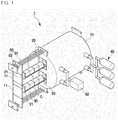
- a thin film deposition system 1includes an external chamber 10, a process chamber 20, doors 11, 21, a cassette holder 30, a connecting member 70, and a shifting unit 60.
- the external chamber 10is formed at one side thereof with an opening 12, through which cassettes C are transferred.
- the external chamber 10receives a plurality of process chambers 20.
- Each of the process chambers 20receives cassettes C, on which substrates are loaded, such that atomic layer deposition is performed on the substrates therein, as described in detail below.
- the process chamberis formed with an opening 22, and includes a first door 21 to open or close the opening and a second door 11 to open or close the opening 12 of the external chamber.
- the first door 21is connected to the second door 11 by a connecting member 70.
- this configurationwill be described in more detail.
- the distance (t1) between the first door 21 and the second door 11is greater than the distance (t2) between the opening 12 of the external chamber and the opening 22 of process chamber (t1>t2).
- the first door 21is provided at an inner wall thereof with a cassette holder 30 capable of loading a plurality of cassettes C.
- the second door 11, the first door 21 and the cassette holder 30are fixedly connected to one another, and the process chamber further includes a shifting unit 60 which reciprocates the first and second doors and the cassette holder in a horizontal direction at the same time.
- the shifting unit 60includes a screw 61 such as a typical ball-screw member, a nut member 62 reciprocating upon rotation of the screw 61, a jig 63 connecting the nut member 62 to the second door 11, and a drive source (not shown) for rotating the screw 61.
- a screw 61such as a typical ball-screw member
- a nut member 62reciprocating upon rotation of the screw 61
- a jig 63connecting the nut member 62 to the second door 11
- a drive source(not shown) for rotating the screw 61.
- the systemfurther includes a gas supply unit 40, which supplies a source gas and a purge gas into the process chambers 20 through the external chamber 10, and an exhaust unit 50 which exhausts gas from the process chambers 20.
- the systemmay further include a heater between the external chamber 10 and the process chambers 20.
- the heatermaintains the process chambers 20 at constant temperature.
- the connecting member 70 connecting the first door 21 to the second door 11is made of an elastically stretchable pogo pin member.
- the connecting member 70includes a large diameter section 71 secured to the second door 11, a small diameter section 72 secured to the first door 21, and a compressive spring 73 which elastically supports the small diameter section 72 within the large diameter section 71.
- the connecting member 70 realized by the pogo pin memberis further provided at an outer periphery thereof with another compressive spring 74 which has a higher coefficient of elasticity than the compressive spring 73.
- the distance between the first door 21 and the second door 11may be changed instead of being fixed, so that the first door 21 and the second door 11 may approach each other or may move apart from each other.
- each of the first and second doors 21, 11is provided with a sealing member 11a or 21b, which may be realized by a mechanical seal, an O-ring, or other sealing members known in the art.
- the sealing member 21a of the first door 21is a mechanical seal and the sealing member 11a of the second door is an O-ring.
- Fig. 4shows a cassette C loaded in the process chamber 20.
- a plurality of substratesis loaded in a standing posture (in a vertical direction or inclined at a certain angle with respect to the vertical direction) in the cassette C.
- a plurality of cassettes C receiving substratesis mounted on the cassette holder 30 connected to one side of the first door 21 (see Fig. 2 ).
- the screw 61when the screw 61 is rotated by primarily driving the drive source, the nut member 62 linearly moves to allow the first and second door 21, 11 connected to each other to move, so that the first door 21 closes the opening 22 of the process chamber.
- the cassette holder 30enters the process chamber 20, so that the cassettes C are transferred into the process chamber 20 by the cassette holder.
- the second door 11does not contact a sidewall of the external chamber 10 (see Fig. 5 ).
- the second door 11linearly moves by the same method as described above, so that the second door 11 closes the opening 12 of the external chamber 10.
- the first door 21 and the cassette holder 30are in the same state as that shown in Fig. 6 , and the connecting member 70 connecting the first door 21 to the second door 11 is contracted as the compressive springs 73, 74 are contracted (see Fig. 6 ).
- source gas and purge gasare alternately supplied into the process chamber to perform atomic layer deposition with respect to the substrates.
- transfer of the cassettes (or substrates) and closing of the external chamber and the process chamberare performed at the same time.
- the distance between the first door and the second doormay be smaller than the distance between the opening of the process chamber and the opening of the external chamber.
- the second dooris moved to close the opening of the external chamber through primary driving of the drive source, and the first door is then moved to close the process chamber through secondary driving of the drive source.
- the thin film deposition systemmay eliminate the external chamber.
- the second door for opening or closing the external chamber and the connecting member for connecting the second door to the first doorare also eliminated, and the shifting unit may be directly connected to the first door.
- the cassette holderis connected to the inner wall of the first door.
- the cassettesmay be transferred into the process chamber when the first door closes the process chamber.
- transfer of the cassettes (or substrates) and closing of the process chamberare also performed at the same time.
- a plurality of cassettes C each receiving substrates S arranged in a standing postureis transferred in an in-line arrangement so as to allow simultaneous processing of the plurality of substrates.
- plural rows of substratesare disposed in an in-line arrangement within the process chamber. Further, respective spaces between the rows of substrates provide gas flow passages.
- the cassettes Cwhen the cassettes C are placed in the process chamber 20, the cassettes C are disposed such that the distance between each cassette and the sidewall of the process chamber or the distance between the respective substrates received in each of the cassettes C becomes a distance between laminar flows.
- laminar flowrefers to a flow of gas supplied into a narrow space and moving in a certain direction without free diffusion and substantially no scattering.
- the term "distance between laminar flows”refers to a distance between two laminar flows of gas. In this embodiment, the distance between laminar flows is 0.2 to 10 mm. If the distance between laminar flows is less than 0.2 mm, the system has difficulty not only in processing and manufacture, but also in control of gas supply. If the distance between laminar flows exceeds 10 mm, the laminar flow of gas is not maintained, causing free diffusion of the gas.
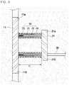
- a gas diffusion supply section 42is formed on one sidewall 28 of the process chamber 20 to transfer gas to a leading end of the sidewall along the sidewall when supplied through a gas supply port 27.
- the gas diffusion supply section 42includes a recess 41 formed like a step on an outer surface of the one sidewall 28 of the process chamber, and a lid 43 closing the recess 41.
- a recess 41formed like a step on an outer surface of the one sidewall 28 of the process chamber
- a lid 43closing the recess 41.
- the recess 41is covered with the lid 43
- the lid 43is separated from a bottom surface of the recess 41 to define a space for gas flow between the recess 41 and the lid 43.
- the gas diffusion supply section 42may be formed on any sidewall of the process chamber 20 such as an upper, lower, right or left sidewall 23, 24, 28 or 29.
- the gas diffusion supply section 42is formed to have a cross-sectional area gradually increasing from the gas supply port 27 on the sidewall 28 towards the leading end thereof. This configuration allows uniform distribution of gas before the gas reaches the front side of the process chamber 20 through the gas diffusion supply section 42. Further, while passing through the gas diffusion supply section 42, the gas supplied through the gas supply port 27 maintains a laminar flow. Thus, the distance between the gas diffusion supply section 42 and the lid 43 is set to maintain a laminar gas flow.
- the gasflows to the front side of the process chamber (that is, to the leading end of the sidewall) along the gas diffusion supply section 42 while being uniformly diffused by the gas diffusion supply section 42.
- the gas sufficiently diffused along the gas diffusion supply section 42moves as a laminar gas flow towards an opposite sidewall along a straight gas supply groove formed on the front side of the process chamber 20.
- the gasAfter reaching front sides of the substrates, that is, the straight gas supply groove, the gas forms a thin film on each of the substrates while moving as a laminar flow through spaces between the respective rows of substrates.
- the space between the respective rows of substratesconstitutes a flow passage which maintains the distance between laminar flows so as to allow gas to move as a laminar flow within the process chamber.
- the plurality of cassettes C1 to C4is disposed adjacent each other in an in-line arrangement, and substrates S1 to S4 received in adjacent cassettes are also arranged adjacent each other, so that the gas uniformly flows in the plurality of cassettes while maintaining a laminar flow.
- a purge gasis supplied immediately after the first reaction gas into the process chamber, so that the first reaction gas and the purge gas coexist within the single vacuum chamber while virtually dividing the internal space of the vacuum chamber.
- a first reaction gas spacerefers to an imaginary space of the process chamber filled with the first reaction gas
- a first purge gas spacerefers to an imaginary space of the process chamber filled with the purge gas and consecutive to the first reaction gas space
- a second reaction gasrefers to an imaginary space of the process chamber filled with a second reaction gas
- a second purge gas spacerefers to an imaginary space of the process chamber filled with the purge gas and consecutive to the second reaction gas.
- the first reaction gas space, the first purge gas space, the second reaction gas space, and the second purge gas spacemove at a predetermined rate in a predetermined direction at the same time instead of remaining at certain places.
- the imaginary first reaction gas space filled with the first reaction gasis created within the vacuum chamber and moves from one space to the other space within the process chamber.
- the first purge gas space consecutive to the first reaction gas spaceis created within the vacuum chamber and follows the first reaction gas space while pushing the first reaction gas in the moving direction thereof.
- an interface between the first reaction gas space and the first purge gas spaceis not clearly formed, and a mixed section between the first reaction gas and the purge gas may be present at the interface.
- the concentration of the first reaction gasgradually increases towards the center of the first reaction gas space, and the concentration of the purge gas gradually increases towards the center of the first purge gas space.
- the purge gas forming the first purge gas spaceis supplied in a much greater amount than the first reaction gas, such that the first reaction gas is moved in an opposite direction relative to the straight gas supply groove by movement of the first purge gas.
- the second reaction gas spaceis formed consecutive to the first purge gas space by supplying a second reaction gas.
- the second purge gas spaceis formed consecutive to the second reaction gas space by supplying a large amount of purge gas, so that the second reaction gas may be completely removed by movement of the second purge gas space.
- reaction gas supply and purgingare consecutively performed like a process of scanning substrates within a single process chamber, thereby significantly reducing process time while substantially increasing throughput, as compared with a conventional process in which reaction gas supply and purging are intermittently performed with respect to the overall inner space of the process chamber.
- the above processmay be repeatedly performed through a plurality of cycles as needed. It should be understood that exhaust operation is carried out during supply of the respective gases.
- the thin film deposition systemincludes a process chamber and cassettes arranged to form a laminar gas flow in the process chamber virtually divided into several spaces when a reaction gas and a purge gas are subsequently supplied into the process chamber, such that atomic layer deposition is sequentially performed on a plurality of substrates loaded within the process chamber while the virtually divided spaces are moved in a scanning manner within the process chamber, thereby reducing a process tack time.
- the thin film deposition systemallows atomic layer deposition to be consecutively performed while a reaction gas and a purge gas are sequentially supplied into the single process chamber instead of performing separate pumping or purging operation with respect to each of reaction gases in the process chamber.
- substratesare arranged in plural rows in order to supply gas to a space between the substrate, thereby enabling formation of a uniform thin film.
- doors for opening or closing the process chamberare integrally formed with a cassette holder, so that cassettes can be loaded or unloaded simultaneously with opening or closing of the process chamber.
Landscapes
- Chemical & Material Sciences (AREA)
- General Chemical & Material Sciences (AREA)
- Chemical Kinetics & Catalysis (AREA)
- Engineering & Computer Science (AREA)
- Materials Engineering (AREA)
- Mechanical Engineering (AREA)
- Metallurgy (AREA)
- Organic Chemistry (AREA)
- Physics & Mathematics (AREA)
- Fluid Mechanics (AREA)
- Chemical Vapour Deposition (AREA)
Description
- Embodiments of the invention relate to a method and system for thin film deposition, and more specifically, to a method and system for thin film deposition, which includes a process chamber configured to provide a laminar gas flow and virtually divided into several spaces when a reaction gas and a purge gas are consecutively supplied into the process chamber, so that atomic layer deposition can be performed with respect to a plurality of substrates while the virtually divided spaces are moved within the process chamber, thereby reducing a process tack time.
- Generally, semiconductor devices or flat display panels are manufactured through various processes. In particular, a process of depositing a thin film on a wafer or glass (hereinafter referred to as a 'substrate') is inevitably carried out. Such thin film deposition is realized by sputtering, chemical vapor deposition (CVD), atomic layer deposition (ALD), and the like.
- In particular, atomic layer deposition (ALD) is a process of depositing a thin film in units of an atomic layer through decomposition and adsorption of two or more reactants by sequentially inputting the reactants into a process chamber used for forming a thin film. Specifically, a first reaction gas is supplied in a pulsing manner into the chamber to be chemically deposited to a lower layer of the substrate within the chamber and the remaining first reaction gas physically coupled thereto is removed in a purging manner. Then, a second reaction gas is also supplied and removed through pulsing and purging, such that a desired thin film can be deposited on the substrate through chemical reaction between some of the second reaction gas with the first reaction gas (that is, a first reactant). Examples of thin films produced by atomic layer deposition include Al2O3, Ta2O3, TiO2, and Si3N4 thin films.
- Since atomic layer deposition enables formation of a thin film having good step coverage even at low temperature of 600 °C or less, it is expected that the atomic layer deposition will be widely applied to manufacture of next generation semiconductor devices. In the atomic layer deposition described above, a duration for which the respective gases perform pulsing and purging once is referred to as a cycle.
- However, since a conventional apparatus for atomic layer deposition supplies gas in a dot pattern through a spray hole of a diffusing plate instead of a plane pattern, the gas is not uniformly distributed within the process chamber, thereby deteriorating uniformity of the thin film.
- For example,
US 2009/0297710 A1 discloses an atomic layer deposition apparatus in which gas flow is first conducted vertically in a bottom-to-top direction, horizontally, to then pass through a mesh and enter in the reaction chamber. The gas flows then vertically in a top-to-bottom direction in between the vertically placed substrates. InUS 2008/0026251 A1 , the gas is fed to the reaction chamber through a plurality of nozzles extending from bottom to top along the inner wall of the reaction chamber and are provided with a great number of holes arranged in the vertical direction and in parallel with the substrate.US 2003/0140854 A1 discloses an atomic layer epitaxy apparatus comprising a sprayhead that includes the reactant and the protective gas infeed channels, attached to the top of the reaction chamber. InUS 2010/0166955 A1 , gas is delivered to the reaction chamber through an input plenum which allows gas volume increase to reduce gas flow velocity and gas pressure prior to the gas reaching the reaction chamber so that gas flow into the reaction chamber is less turbulent. - The present invention is conceived to solve the problems as described above, and aspects of the present invention are to provide a method according to
claim 5 and system according to claim 1 for thin film deposition, which includes a process chamber configured to provide a laminar gas flow and virtually divided into several spaces when a reaction gas and a purge gas are consecutively supplied into the process chamber, so that atomic layer deposition can be performed with respect to a plurality of substrates while the virtually divided spaces are moved within the process chamber, thereby reducing process tack time. - In accordance with one aspect of the invention, a thin film deposition system includes an external chamber having an opening at one side thereof; a process chamber disposed inside the external chamber and having an opening at one side thereof; a first door opening or closing the opening of the process chamber; a cassette holder connected to an inner wall of the first door and loading at least one cassette thereon; a second door opening or closing the opening of the external chamber; a connecting member connecting the first door to the second door; and a shifting unit horizontally reciprocating the first door and the cassette holder together with the second door.
- In accordance with another aspect of the invention, a thin film deposition system may include a cassette loading a plurality of substrates such that the substrates are separated constant distances from each other and the distance between the respective substrates becomes a distance between laminar flows; a process chamber which receives the cassette such that a distance between the cassette and an inner wall of the process chamber becomes the distance between laminar flows, and in which the substrates are subjected to atomic layer deposition; a gas supply unit disposed at one sidewall of the process chamber and supplying gas to all of the substrates placed in the cassette in a direction parallel to arrangement of the substrates such that a laminar flow of the gas is provided to leading ends of the substrates, to a space between the substrates, and to a space between the substrate and the wall of the process chamber; and a gas exhaust unit disposed at an opposite side with respect to the gas supply unit in the process chamber and discharging the gas from the process chamber by suctioning the gas at rear sides of the substrates.
- The above and other aspects, features and advantages of the invention will become apparent from the following description of embodiments given in conjunction with the accompanying drawings, in which:
Fig. 1 is a perspective view of a thin film deposition system according to one embodiment of the present invention;Fig. 2 is a sectional view of the thin film deposition system according to the exemplary embodiment of the present invention;Fig. 3 is a sectional view of a connecting member of the thin film deposition system according to the embodiment of the present invention;Fig. 4 is a sectional view of a cassette loaded in a process chamber of the thin film deposition system according to the embodiment of the present invention;Fig. 5 is a sectional view of the thin film deposition system according to the embodiment of the present invention;Fig. 6 is a sectional view of the thin film deposition system according to the embodiment of the present invention; andFigs. 7 and8 are views of the process chamber of the thin film deposition system according to the embodiment of the present invention.- Exemplary embodiments of the present invention will now be described in detail with reference to the accompanying drawings.
- Referring to
Figs. 1 and2 , a thin film deposition system 1 according to one embodiment of the invention includes anexternal chamber 10, aprocess chamber 20,doors cassette holder 30, a connectingmember 70, and ashifting unit 60. - The
external chamber 10 is formed at one side thereof with anopening 12, through which cassettes C are transferred. Theexternal chamber 10 receives a plurality ofprocess chambers 20. - Each of the
process chambers 20 receives cassettes C, on which substrates are loaded, such that atomic layer deposition is performed on the substrates therein, as described in detail below. - The process chamber is formed with an opening 22, and includes a
first door 21 to open or close the opening and asecond door 11 to open or close the opening 12 of the external chamber. Thefirst door 21 is connected to thesecond door 11 by a connectingmember 70. Next, this configuration will be described in more detail. Here, the distance (t1) between thefirst door 21 and thesecond door 11 is greater than the distance (t2) between the opening 12 of the external chamber and the opening 22 of process chamber (t1>t2). - In addition, the
first door 21 is provided at an inner wall thereof with acassette holder 30 capable of loading a plurality of cassettes C. - As such, the
second door 11, thefirst door 21 and thecassette holder 30 are fixedly connected to one another, and the process chamber further includes a shiftingunit 60 which reciprocates the first and second doors and the cassette holder in a horizontal direction at the same time. - The shifting
unit 60 includes ascrew 61 such as a typical ball-screw member, anut member 62 reciprocating upon rotation of thescrew 61, ajig 63 connecting thenut member 62 to thesecond door 11, and a drive source (not shown) for rotating thescrew 61. - The system further includes a
gas supply unit 40, which supplies a source gas and a purge gas into theprocess chambers 20 through theexternal chamber 10, and anexhaust unit 50 which exhausts gas from theprocess chambers 20. - Although not shown in the drawings, the system may further include a heater between the
external chamber 10 and theprocess chambers 20. The heater maintains theprocess chambers 20 at constant temperature. - Main components of the thin film deposition system according to this embodiment will be described in more detail with reference to
Fig. 3 . Referring toFig. 3 , the connectingmember 70 connecting thefirst door 21 to thesecond door 11 is made of an elastically stretchable pogo pin member. Specifically, the connectingmember 70 includes alarge diameter section 71 secured to thesecond door 11, asmall diameter section 72 secured to thefirst door 21, and acompressive spring 73 which elastically supports thesmall diameter section 72 within thelarge diameter section 71. Further, the connectingmember 70 realized by the pogo pin member is further provided at an outer periphery thereof with anothercompressive spring 74 which has a higher coefficient of elasticity than thecompressive spring 73. Thus, the distance between thefirst door 21 and thesecond door 11 may be changed instead of being fixed, so that thefirst door 21 and thesecond door 11 may approach each other or may move apart from each other. - Further, each of the first and
second doors member member 21a of thefirst door 21 is a mechanical seal and the sealingmember 11a of the second door is an O-ring. Fig. 4 shows a cassette C loaded in theprocess chamber 20. Referring toFig. 4 , a plurality of substrates is loaded in a standing posture (in a vertical direction or inclined at a certain angle with respect to the vertical direction) in the cassette C.- Next, operation of the thin film deposition system will be described with reference to
Figs. 2 ,5 and6 . - First, with the first and
second doors cassette holder 30 connected to one side of the first door 21 (seeFig. 2 ). - Next, when the
screw 61 is rotated by primarily driving the drive source, thenut member 62 linearly moves to allow the first andsecond door first door 21 closes the opening 22 of the process chamber. At the same time, thecassette holder 30 enters theprocess chamber 20, so that the cassettes C are transferred into theprocess chamber 20 by the cassette holder. In this stage, thesecond door 11 does not contact a sidewall of the external chamber 10 (seeFig. 5 ). - Next, when the
screw 61 is rotated by secondarily driving the drive source, thesecond door 11 linearly moves by the same method as described above, so that thesecond door 11 closes the opening 12 of theexternal chamber 10. However, thefirst door 21 and thecassette holder 30 are in the same state as that shown inFig. 6 , and the connectingmember 70 connecting thefirst door 21 to thesecond door 11 is contracted as thecompressive springs Fig. 6 ). - As such, with the cassettes C transferred into the
process chamber 20 and theexternal chamber 10 and theprocess chamber 20 closed, source gas and purge gas are alternately supplied into the process chamber to perform atomic layer deposition with respect to the substrates. - Thus, in this embodiment, transfer of the cassettes (or substrates) and closing of the external chamber and the process chamber are performed at the same time.
- Obviously, the above description of the embodiment is provided for illustration only and various modifications and changes can be made without departing from the present invention. For example, the distance between the first door and the second door may be smaller than the distance between the opening of the process chamber and the opening of the external chamber. In this case, the second door is moved to close the opening of the external chamber through primary driving of the drive source, and the first door is then moved to close the process chamber through secondary driving of the drive source.
- In another embodiment, the thin film deposition system may eliminate the external chamber. In this case, the second door for opening or closing the external chamber and the connecting member for connecting the second door to the first door are also eliminated, and the shifting unit may be directly connected to the first door. In this embodiment, the cassette holder is connected to the inner wall of the first door. Thus, the cassettes may be transferred into the process chamber when the first door closes the process chamber. Thus, in this embodiment, transfer of the cassettes (or substrates) and closing of the process chamber are also performed at the same time.
- Next, referring to
Figs. 7 and8 , theprocess chamber 20 according to the embodiment will be described in more detail. Within theprocess chamber 20, a plurality of cassettes C each receiving substrates S arranged in a standing posture (in a vertical direction or inclined at a certain angle to the vertical direction) is transferred in an in-line arrangement so as to allow simultaneous processing of the plurality of substrates. - In other words, plural rows of substrates are disposed in an in-line arrangement within the process chamber. Further, respective spaces between the rows of substrates provide gas flow passages.
- Specifically, in this embodiment, when the cassettes C are placed in the
process chamber 20, the cassettes C are disposed such that the distance between each cassette and the sidewall of the process chamber or the distance between the respective substrates received in each of the cassettes C becomes a distance between laminar flows. - As used herein, the term "laminar flow" refers to a flow of gas supplied into a narrow space and moving in a certain direction without free diffusion and substantially no scattering.
- Further, as used herein, the term "distance between laminar flows" refers to a distance between two laminar flows of gas. In this embodiment, the distance between laminar flows is 0.2 to 10 mm. If the distance between laminar flows is less than 0.2 mm, the system has difficulty not only in processing and manufacture, but also in control of gas supply. If the distance between laminar flows exceeds 10 mm, the laminar flow of gas is not maintained, causing free diffusion of the gas.
- According to this embodiment, not only the space between the substrates S within each of the cassettes C, but also the space between each cassette C and each wall of the chamber and the space between the leading ends of the cassettes C or substrates S and a straight gas supply groove are set corresponding to the distance between laminar flows.
- A gas
diffusion supply section 42 is formed on onesidewall 28 of theprocess chamber 20 to transfer gas to a leading end of the sidewall along the sidewall when supplied through agas supply port 27. - The gas
diffusion supply section 42 includes arecess 41 formed like a step on an outer surface of the onesidewall 28 of the process chamber, and alid 43 closing therecess 41. Of course, although therecess 41 is covered with thelid 43, thelid 43 is separated from a bottom surface of therecess 41 to define a space for gas flow between therecess 41 and thelid 43. - The gas
diffusion supply section 42 may be formed on any sidewall of theprocess chamber 20 such as an upper, lower, right or leftsidewall - The gas
diffusion supply section 42 is formed to have a cross-sectional area gradually increasing from thegas supply port 27 on thesidewall 28 towards the leading end thereof. This configuration allows uniform distribution of gas before the gas reaches the front side of theprocess chamber 20 through the gasdiffusion supply section 42. Further, while passing through the gasdiffusion supply section 42, the gas supplied through thegas supply port 27 maintains a laminar flow. Thus, the distance between the gasdiffusion supply section 42 and thelid 43 is set to maintain a laminar gas flow. - Next, operation of the process chamber according to this embodiment will be described.
- First, when gas is supplied to the
gas supply port 27 formed on one sidewall of theprocess chamber 20 from a gas supply unit, the gas flows to the front side of the process chamber (that is, to the leading end of the sidewall) along the gasdiffusion supply section 42 while being uniformly diffused by the gasdiffusion supply section 42. - Then, the gas sufficiently diffused along the gas
diffusion supply section 42 moves as a laminar gas flow towards an opposite sidewall along a straight gas supply groove formed on the front side of theprocess chamber 20. - After reaching front sides of the substrates, that is, the straight gas supply groove, the gas forms a thin film on each of the substrates while moving as a laminar flow through spaces between the respective rows of substrates.
- Accordingly, the space between the respective rows of substrates constitutes a flow passage which maintains the distance between laminar flows so as to allow gas to move as a laminar flow within the process chamber. Further, within the process chamber, the plurality of cassettes C1 to C4 is disposed adjacent each other in an in-line arrangement, and substrates S1 to S4 received in adjacent cassettes are also arranged adjacent each other, so that the gas uniformly flows in the plurality of cassettes while maintaining a laminar flow.
- In this embodiment, instead of performing operation of pumping or purging the first reaction gas from the process chamber after stopping supply of a first reaction gas, a purge gas is supplied immediately after the first reaction gas into the process chamber, so that the first reaction gas and the purge gas coexist within the single vacuum chamber while virtually dividing the internal space of the vacuum chamber.
- In this embodiment, a first reaction gas space refers to an imaginary space of the process chamber filled with the first reaction gas, and a first purge gas space refers to an imaginary space of the process chamber filled with the purge gas and consecutive to the first reaction gas space. Further, a second reaction gas refers to an imaginary space of the process chamber filled with a second reaction gas, and a second purge gas space refers to an imaginary space of the process chamber filled with the purge gas and consecutive to the second reaction gas. According to this embodiment, the first reaction gas space, the first purge gas space, the second reaction gas space, and the second purge gas space move at a predetermined rate in a predetermined direction at the same time instead of remaining at certain places.
- Specifically, a process of forming the gas spaces will be described hereinafter. First, when the first reaction gas is supplied to the process chamber, the imaginary first reaction gas space filled with the first reaction gas is created within the vacuum chamber and moves from one space to the other space within the process chamber.
- Then, when a purge gas is supplied after stopping supply of the first reaction gas, the first purge gas space consecutive to the first reaction gas space is created within the vacuum chamber and follows the first reaction gas space while pushing the first reaction gas in the moving direction thereof. Here, an interface between the first reaction gas space and the first purge gas space is not clearly formed, and a mixed section between the first reaction gas and the purge gas may be present at the interface. Further, the concentration of the first reaction gas gradually increases towards the center of the first reaction gas space, and the concentration of the purge gas gradually increases towards the center of the first purge gas space.
- As described above, according to this embodiment, in order to achieve complete purging of the first reaction gas from the process chamber, the purge gas forming the first purge gas space is supplied in a much greater amount than the first reaction gas, such that the first reaction gas is moved in an opposite direction relative to the straight gas supply groove by movement of the first purge gas.
- Then, the second reaction gas space is formed consecutive to the first purge gas space by supplying a second reaction gas. Further, the second purge gas space is formed consecutive to the second reaction gas space by supplying a large amount of purge gas, so that the second reaction gas may be completely removed by movement of the second purge gas space.
- As such, according to this embodiment, atomic layer deposition is carried out while the first reaction gas space, the first purge gas space, the second reaction gas space and the second purge gas space sequentially move within the process chamber. Thus, according to this embodiment, reaction gas supply and purging are consecutively performed like a process of scanning substrates within a single process chamber, thereby significantly reducing process time while substantially increasing throughput, as compared with a conventional process in which reaction gas supply and purging are intermittently performed with respect to the overall inner space of the process chamber.
- Further, the above process may be repeatedly performed through a plurality of cycles as needed. It should be understood that exhaust operation is carried out during supply of the respective gases.
- As described above, according to the embodiment, the thin film deposition system includes a process chamber and cassettes arranged to form a laminar gas flow in the process chamber virtually divided into several spaces when a reaction gas and a purge gas are subsequently supplied into the process chamber, such that atomic layer deposition is sequentially performed on a plurality of substrates loaded within the process chamber while the virtually divided spaces are moved in a scanning manner within the process chamber, thereby reducing a process tack time.
- Namely, the thin film deposition system according to the embodiment allows atomic layer deposition to be consecutively performed while a reaction gas and a purge gas are sequentially supplied into the single process chamber instead of performing separate pumping or purging operation with respect to each of reaction gases in the process chamber.
- In addition, in the deposition system according to the embodiment, substrates are arranged in plural rows in order to supply gas to a space between the substrate, thereby enabling formation of a uniform thin film.
- Further, in the deposition system according to the embodiment, doors for opening or closing the process chamber are integrally formed with a cassette holder, so that cassettes can be loaded or unloaded simultaneously with opening or closing of the process chamber.
- Although some embodiments have been described herein, it will be apparent to those skilled in the art that the embodiments are given by way of illustration and that various modifications, additions, changes and variations can be made without departing from the scope of the invention. Accordingly, the scope of the invention should be limited only by the accompanying claims.
Claims (7)
- A thin film deposition system comprising:a cassette loading a plurality of substrates such that the substrates are separated constant distances from each other and the distance between the respective substrates is between 0.2 and 10 mm;a process chamber which receives the cassette such that a distance between the cassette and an inner wall of the process chamber is the distance between 0.2 and 10 mm, and in which the substrates are subjected to atomic layer deposition;a gas supply unit disposed at one sidewall of the process chamber and supplying gas to all of the substrates placed in the cassette in a direction parallel to arrangement of the substrates such that a laminar flow of the gas is provided to leading ends of the substrates, to a space between the substrates, and to a space between the substrate and the wall of the process chamber; anda gas exhaust unit disposed at an opposite side to the gas supply unit in the process chamber and exhausting the gas from the process chamber by suctioning the gas at rear sides of the substrates.
- The system of claim 1, wherein the gas supply unit comprises a straight gas supply groove formed on the sidewall of the process chamber having the gas supply unit disposed thereon and allows gas to flow from one side of the sidewall to a region including other side thereof in a laminar flow manner through the straight gas supply groove.
- The system of claim 2, wherein the gas supply unit comprises:a gas diffusion supply section formed on a sidewall of the process chamber adjacent to the sidewall having the gas supply unit disposed thereon and supplying gas to the straight gas supply groove through uniform diffusion of the gas over the entirety of one side of the sidewall; anda gas supply port provided to one end of the gas diffusion supply section and supplying the gas to the gas diffusion supply section therethrough.
- The system of claim 1, wherein the distance between the respective substrates and between the cassette and an inner wall of the process chamber is between 0.5 and 10 mm.
- A thin film deposition method comprising:1) placing a cassette loading a plurality of substrates within a process chamber such that a distance between the substrates and a distance between the cassette and the process chamber is between 0.2 and 10 mm, followed by exhausting gas from the process chamber;2) supplying a first reaction gas into the process chamber such that a first reaction gas space occupied by the first reaction gas sequentially moves from one space to the other space within the process chamber;3) supplying a purge gas into the process chamber simultaneously with blocking of the first reaction gas, such that a first purge gas space is formed consecutive to the first reaction gas space and moves in the same direction as that of the first reaction gas space;4) supplying a second reaction gas into the process chamber simultaneously with blocking of the purge gas, such that a second reaction space is formed consecutive to the first purge gas space and moves in the same direction as that of the first purge gas space; and5) supplying the purge gas into the process chamber simultaneously with blocking of the second reaction gas, such that a second purge gas space is formed consecutive to the second reaction gas space and moves in the same direction as that of the second reaction gas space,wherein an exhaust operation is performed without stopping during operations 1) to 5) in an opposite direction to a direction of supplying the reaction gases and purge gas by suctioning and exhausting the gases from the process chamber.
- The method of claim 5, wherein a cycle of performing the operations 1) to 5) is repeatedly performed.
- The method according to any of cliams 5 and 6, wherein the distance between the substrates and the distance between the cassette and the process chamber is between 0.5 and 10 nm.
Applications Claiming Priority (3)
| Application Number | Priority Date | Filing Date | Title |
|---|---|---|---|
| KR1020100128147AKR101219381B1 (en) | 2010-12-15 | 2010-12-15 | Thin layer deposition method |
| KR1020100128157AKR101173085B1 (en) | 2010-12-15 | 2010-12-15 | Thin layer deposition apparatus |
| KR1020100128158AKR101168150B1 (en) | 2010-12-15 | 2010-12-15 | Thin layer deposition apparatus |
Publications (3)
| Publication Number | Publication Date |
|---|---|
| EP2465972A2 EP2465972A2 (en) | 2012-06-20 |
| EP2465972A3 EP2465972A3 (en) | 2012-09-05 |
| EP2465972B1true EP2465972B1 (en) | 2017-05-03 |
Family
ID=45421911
Family Applications (1)
| Application Number | Title | Priority Date | Filing Date |
|---|---|---|---|
| EP11193595.3AActiveEP2465972B1 (en) | 2010-12-15 | 2011-12-14 | Method and system for thin film deposition |
Country Status (3)
| Country | Link |
|---|---|
| EP (1) | EP2465972B1 (en) |
| CN (1) | CN102560421B (en) |
| TW (1) | TWI475129B (en) |
Families Citing this family (8)
| Publication number | Priority date | Publication date | Assignee | Title |
|---|---|---|---|---|
| US10566226B2 (en) | 2014-11-11 | 2020-02-18 | Applied Materials, Inc. | Multi-cassette carrying case |
| CN107644949B (en)* | 2016-07-21 | 2020-11-24 | Ncd有限公司 | Methods of Forming Inorganic Thin Layers on OLEDs |
| KR102205200B1 (en)* | 2018-09-20 | 2021-01-20 | 주식회사 엔씨디 | A apparatus for depositing a thin layer on the substrate |
| CN109023306A (en)* | 2018-09-30 | 2018-12-18 | 无锡松煜科技有限公司 | Apparatus for atomic layer deposition |
| FI128855B (en)* | 2019-09-24 | 2021-01-29 | Picosun Oy | Fluid distributing device for a thin-film deposition apparatus, related apparatus and methods |
| CN111607780A (en)* | 2020-05-15 | 2020-09-01 | 南京恩腾电子科技有限公司 | Atomic layer deposition method for surface of three-dimensional bluff body |
| FI130279B (en)* | 2021-03-30 | 2023-05-31 | Beneq Oy | Reactor arrangement for atomic layer cultivation and method of operating a reactor arrangement for atomic layer cultivation |
| FI131711B1 (en)* | 2022-03-30 | 2025-10-08 | Beneq Oy | Reaction chamber, atomic layer deposition apparatus and method |
Family Cites Families (8)
| Publication number | Priority date | Publication date | Assignee | Title |
|---|---|---|---|---|
| FI118474B (en)* | 1999-12-28 | 2007-11-30 | Asm Int | Apparatus for making thin films |
| US6936086B2 (en)* | 2002-09-11 | 2005-08-30 | Planar Systems, Inc. | High conductivity particle filter |
| JP4475136B2 (en)* | 2005-02-18 | 2010-06-09 | 東京エレクトロン株式会社 | Processing system, pre-processing apparatus and storage medium |
| US7883746B2 (en)* | 2006-07-27 | 2011-02-08 | Panasonic Corporation | Insulating film formation method which exhibits improved thickness uniformity and improved composition uniformity |
| CN100590803C (en)* | 2007-06-22 | 2010-02-17 | 中芯国际集成电路制造(上海)有限公司 | Atomic layer deposition method and formed semiconductor device |
| US10041169B2 (en)* | 2008-05-27 | 2018-08-07 | Picosun Oy | System and method for loading a substrate holder carrying a batch of vertically placed substrates into an atomic layer deposition reactor |
| DE102008034330A1 (en)* | 2008-07-23 | 2010-01-28 | Ionbond Ag Olten | CVD reactor for the separation of layers of a reaction gas mixture on workpieces |
| US9328417B2 (en)* | 2008-11-01 | 2016-05-03 | Ultratech, Inc. | System and method for thin film deposition |
- 2011
- 2011-12-14EPEP11193595.3Apatent/EP2465972B1/enactiveActive
- 2011-12-14TWTW100146079Apatent/TWI475129B/enactive
- 2011-12-15CNCN201110434373.6Apatent/CN102560421B/enactiveActive
Also Published As
| Publication number | Publication date |
|---|---|
| TWI475129B (en) | 2015-03-01 |
| CN102560421A (en) | 2012-07-11 |
| EP2465972A2 (en) | 2012-06-20 |
| TW201235505A (en) | 2012-09-01 |
| EP2465972A3 (en) | 2012-09-05 |
| CN102560421B (en) | 2014-12-10 |
Similar Documents
| Publication | Publication Date | Title |
|---|---|---|
| EP2465972B1 (en) | Method and system for thin film deposition | |
| US11742189B2 (en) | Multi-zone reactor, system including the reactor, and method of using the same | |
| US10184179B2 (en) | Atomic layer deposition processing chamber permitting low-pressure tool replacement | |
| US20150368798A1 (en) | Apparatus And Process Containment For Spatially Separated Atomic Layer Deposition | |
| US20120225191A1 (en) | Apparatus and Process for Atomic Layer Deposition | |
| TWI821314B (en) | Gas distribution assembly for improved pump-purge and precursor delivery | |
| CN108220921A (en) | Film formation device and film build method | |
| KR102349330B1 (en) | Thin film encapsulation processing system and process kit | |
| US11306393B2 (en) | Methods and apparatus for ALD processes | |
| KR101573689B1 (en) | The apparatus for depositing the atomic layer | |
| KR101698021B1 (en) | A ald apparatus for large substrate | |
| KR101610644B1 (en) | The apparatus for depositing the atomic layer | |
| KR101393463B1 (en) | Thin layer deposition apparatus | |
| KR101173085B1 (en) | Thin layer deposition apparatus | |
| KR101573687B1 (en) | The apparatus for depositing the atomic layer | |
| KR20150109778A (en) | Multi-type deposition apparatus and methode thereof | |
| KR101145058B1 (en) | Atomic layer deposition apparatus | |
| KR20150081590A (en) | The method for depositing a atomic layer on the large substrate | |
| KR20150081596A (en) | The apparatus for depositing the atomic layer | |
| KR20120066851A (en) | Thin layer deposition method |
Legal Events
| Date | Code | Title | Description |
|---|---|---|---|
| PUAI | Public reference made under article 153(3) epc to a published international application that has entered the european phase | Free format text:ORIGINAL CODE: 0009012 | |
| AK | Designated contracting states | Kind code of ref document:A2 Designated state(s):AL AT BE BG CH CY CZ DE DK EE ES FI FR GB GR HR HU IE IS IT LI LT LU LV MC MK MT NL NO PL PT RO RS SE SI SK SM TR | |
| AX | Request for extension of the european patent | Extension state:BA ME | |
| PUAL | Search report despatched | Free format text:ORIGINAL CODE: 0009013 | |
| RIC1 | Information provided on ipc code assigned before grant | Ipc:C23C 16/455 20060101ALI20120724BHEP Ipc:C23C 16/54 20060101AFI20120724BHEP | |
| AK | Designated contracting states | Kind code of ref document:A3 Designated state(s):AL AT BE BG CH CY CZ DE DK EE ES FI FR GB GR HR HU IE IS IT LI LT LU LV MC MK MT NL NO PL PT RO RS SE SI SK SM TR | |
| AX | Request for extension of the european patent | Extension state:BA ME | |
| 17P | Request for examination filed | Effective date:20130305 | |
| 17Q | First examination report despatched | Effective date:20151008 | |
| GRAP | Despatch of communication of intention to grant a patent | Free format text:ORIGINAL CODE: EPIDOSNIGR1 | |
| INTG | Intention to grant announced | Effective date:20161121 | |
| RIN1 | Information on inventor provided before grant (corrected) | Inventor name:CHOI, KYU-JEONG Inventor name:SHIN, WOONG CHUL Inventor name:BAEK, MIN | |
| GRAS | Grant fee paid | Free format text:ORIGINAL CODE: EPIDOSNIGR3 | |
| GRAA | (expected) grant | Free format text:ORIGINAL CODE: 0009210 | |
| AK | Designated contracting states | Kind code of ref document:B1 Designated state(s):AL AT BE BG CH CY CZ DE DK EE ES FI FR GB GR HR HU IE IS IT LI LT LU LV MC MK MT NL NO PL PT RO RS SE SI SK SM TR | |
| REG | Reference to a national code | Ref country code:GB Ref legal event code:FG4D | |
| REG | Reference to a national code | Ref country code:AT Ref legal event code:REF Ref document number:890084 Country of ref document:AT Kind code of ref document:T Effective date:20170515 Ref country code:CH Ref legal event code:EP | |
| REG | Reference to a national code | Ref country code:IE Ref legal event code:FG4D | |
| REG | Reference to a national code | Ref country code:DE Ref legal event code:R096 Ref document number:602011037506 Country of ref document:DE | |
| REG | Reference to a national code | Ref country code:NL Ref legal event code:MP Effective date:20170503 | |
| REG | Reference to a national code | Ref country code:AT Ref legal event code:MK05 Ref document number:890084 Country of ref document:AT Kind code of ref document:T Effective date:20170503 | |
| REG | Reference to a national code | Ref country code:LT Ref legal event code:MG4D | |
| PG25 | Lapsed in a contracting state [announced via postgrant information from national office to epo] | Ref country code:FI Free format text:LAPSE BECAUSE OF FAILURE TO SUBMIT A TRANSLATION OF THE DESCRIPTION OR TO PAY THE FEE WITHIN THE PRESCRIBED TIME-LIMIT Effective date:20170503 Ref country code:LT Free format text:LAPSE BECAUSE OF FAILURE TO SUBMIT A TRANSLATION OF THE DESCRIPTION OR TO PAY THE FEE WITHIN THE PRESCRIBED TIME-LIMIT Effective date:20170503 Ref country code:NO Free format text:LAPSE BECAUSE OF FAILURE TO SUBMIT A TRANSLATION OF THE DESCRIPTION OR TO PAY THE FEE WITHIN THE PRESCRIBED TIME-LIMIT Effective date:20170803 Ref country code:ES Free format text:LAPSE BECAUSE OF FAILURE TO SUBMIT A TRANSLATION OF THE DESCRIPTION OR TO PAY THE FEE WITHIN THE PRESCRIBED TIME-LIMIT Effective date:20170503 Ref country code:HR Free format text:LAPSE BECAUSE OF FAILURE TO SUBMIT A TRANSLATION OF THE DESCRIPTION OR TO PAY THE FEE WITHIN THE PRESCRIBED TIME-LIMIT Effective date:20170503 Ref country code:AT Free format text:LAPSE BECAUSE OF FAILURE TO SUBMIT A TRANSLATION OF THE DESCRIPTION OR TO PAY THE FEE WITHIN THE PRESCRIBED TIME-LIMIT Effective date:20170503 Ref country code:GR Free format text:LAPSE BECAUSE OF FAILURE TO SUBMIT A TRANSLATION OF THE DESCRIPTION OR TO PAY THE FEE WITHIN THE PRESCRIBED TIME-LIMIT Effective date:20170804 | |
| PG25 | Lapsed in a contracting state [announced via postgrant information from national office to epo] | Ref country code:BG Free format text:LAPSE BECAUSE OF FAILURE TO SUBMIT A TRANSLATION OF THE DESCRIPTION OR TO PAY THE FEE WITHIN THE PRESCRIBED TIME-LIMIT Effective date:20170803 Ref country code:RS Free format text:LAPSE BECAUSE OF FAILURE TO SUBMIT A TRANSLATION OF THE DESCRIPTION OR TO PAY THE FEE WITHIN THE PRESCRIBED TIME-LIMIT Effective date:20170503 Ref country code:NL Free format text:LAPSE BECAUSE OF FAILURE TO SUBMIT A TRANSLATION OF THE DESCRIPTION OR TO PAY THE FEE WITHIN THE PRESCRIBED TIME-LIMIT Effective date:20170503 Ref country code:LV Free format text:LAPSE BECAUSE OF FAILURE TO SUBMIT A TRANSLATION OF THE DESCRIPTION OR TO PAY THE FEE WITHIN THE PRESCRIBED TIME-LIMIT Effective date:20170503 Ref country code:PL Free format text:LAPSE BECAUSE OF FAILURE TO SUBMIT A TRANSLATION OF THE DESCRIPTION OR TO PAY THE FEE WITHIN THE PRESCRIBED TIME-LIMIT Effective date:20170503 Ref country code:IS Free format text:LAPSE BECAUSE OF FAILURE TO SUBMIT A TRANSLATION OF THE DESCRIPTION OR TO PAY THE FEE WITHIN THE PRESCRIBED TIME-LIMIT Effective date:20170903 Ref country code:SE Free format text:LAPSE BECAUSE OF FAILURE TO SUBMIT A TRANSLATION OF THE DESCRIPTION OR TO PAY THE FEE WITHIN THE PRESCRIBED TIME-LIMIT Effective date:20170503 | |
| PG25 | Lapsed in a contracting state [announced via postgrant information from national office to epo] | Ref country code:SK Free format text:LAPSE BECAUSE OF FAILURE TO SUBMIT A TRANSLATION OF THE DESCRIPTION OR TO PAY THE FEE WITHIN THE PRESCRIBED TIME-LIMIT Effective date:20170503 Ref country code:EE Free format text:LAPSE BECAUSE OF FAILURE TO SUBMIT A TRANSLATION OF THE DESCRIPTION OR TO PAY THE FEE WITHIN THE PRESCRIBED TIME-LIMIT Effective date:20170503 Ref country code:CZ Free format text:LAPSE BECAUSE OF FAILURE TO SUBMIT A TRANSLATION OF THE DESCRIPTION OR TO PAY THE FEE WITHIN THE PRESCRIBED TIME-LIMIT Effective date:20170503 Ref country code:RO Free format text:LAPSE BECAUSE OF FAILURE TO SUBMIT A TRANSLATION OF THE DESCRIPTION OR TO PAY THE FEE WITHIN THE PRESCRIBED TIME-LIMIT Effective date:20170503 Ref country code:DK Free format text:LAPSE BECAUSE OF FAILURE TO SUBMIT A TRANSLATION OF THE DESCRIPTION OR TO PAY THE FEE WITHIN THE PRESCRIBED TIME-LIMIT Effective date:20170503 | |
| REG | Reference to a national code | Ref country code:DE Ref legal event code:R097 Ref document number:602011037506 Country of ref document:DE | |
| PG25 | Lapsed in a contracting state [announced via postgrant information from national office to epo] | Ref country code:SM Free format text:LAPSE BECAUSE OF FAILURE TO SUBMIT A TRANSLATION OF THE DESCRIPTION OR TO PAY THE FEE WITHIN THE PRESCRIBED TIME-LIMIT Effective date:20170503 Ref country code:IT Free format text:LAPSE BECAUSE OF FAILURE TO SUBMIT A TRANSLATION OF THE DESCRIPTION OR TO PAY THE FEE WITHIN THE PRESCRIBED TIME-LIMIT Effective date:20170503 | |
| PLBE | No opposition filed within time limit | Free format text:ORIGINAL CODE: 0009261 | |
| STAA | Information on the status of an ep patent application or granted ep patent | Free format text:STATUS: NO OPPOSITION FILED WITHIN TIME LIMIT | |
| 26N | No opposition filed | Effective date:20180206 | |
| PG25 | Lapsed in a contracting state [announced via postgrant information from national office to epo] | Ref country code:SI Free format text:LAPSE BECAUSE OF FAILURE TO SUBMIT A TRANSLATION OF THE DESCRIPTION OR TO PAY THE FEE WITHIN THE PRESCRIBED TIME-LIMIT Effective date:20170503 | |
| REG | Reference to a national code | Ref country code:CH Ref legal event code:PL | |
| GBPC | Gb: european patent ceased through non-payment of renewal fee | Effective date:20171214 | |
| REG | Reference to a national code | Ref country code:IE Ref legal event code:MM4A | |
| PG25 | Lapsed in a contracting state [announced via postgrant information from national office to epo] | Ref country code:MT Free format text:LAPSE BECAUSE OF NON-PAYMENT OF DUE FEES Effective date:20171214 Ref country code:LU Free format text:LAPSE BECAUSE OF NON-PAYMENT OF DUE FEES Effective date:20171214 | |
| REG | Reference to a national code | Ref country code:FR Ref legal event code:ST Effective date:20180831 | |
| REG | Reference to a national code | Ref country code:BE Ref legal event code:MM Effective date:20171231 | |
| PG25 | Lapsed in a contracting state [announced via postgrant information from national office to epo] | Ref country code:FR Free format text:LAPSE BECAUSE OF NON-PAYMENT OF DUE FEES Effective date:20180102 Ref country code:IE Free format text:LAPSE BECAUSE OF NON-PAYMENT OF DUE FEES Effective date:20171214 | |
| PG25 | Lapsed in a contracting state [announced via postgrant information from national office to epo] | Ref country code:GB Free format text:LAPSE BECAUSE OF NON-PAYMENT OF DUE FEES Effective date:20171214 Ref country code:LI Free format text:LAPSE BECAUSE OF NON-PAYMENT OF DUE FEES Effective date:20171231 Ref country code:CH Free format text:LAPSE BECAUSE OF NON-PAYMENT OF DUE FEES Effective date:20171231 Ref country code:BE Free format text:LAPSE BECAUSE OF NON-PAYMENT OF DUE FEES Effective date:20171231 | |
| PG25 | Lapsed in a contracting state [announced via postgrant information from national office to epo] | Ref country code:MC Free format text:LAPSE BECAUSE OF FAILURE TO SUBMIT A TRANSLATION OF THE DESCRIPTION OR TO PAY THE FEE WITHIN THE PRESCRIBED TIME-LIMIT Effective date:20170503 Ref country code:HU Free format text:LAPSE BECAUSE OF FAILURE TO SUBMIT A TRANSLATION OF THE DESCRIPTION OR TO PAY THE FEE WITHIN THE PRESCRIBED TIME-LIMIT; INVALID AB INITIO Effective date:20111214 | |
| PG25 | Lapsed in a contracting state [announced via postgrant information from national office to epo] | Ref country code:CY Free format text:LAPSE BECAUSE OF NON-PAYMENT OF DUE FEES Effective date:20170503 | |
| PG25 | Lapsed in a contracting state [announced via postgrant information from national office to epo] | Ref country code:MK Free format text:LAPSE BECAUSE OF FAILURE TO SUBMIT A TRANSLATION OF THE DESCRIPTION OR TO PAY THE FEE WITHIN THE PRESCRIBED TIME-LIMIT Effective date:20170503 | |
| PG25 | Lapsed in a contracting state [announced via postgrant information from national office to epo] | Ref country code:TR Free format text:LAPSE BECAUSE OF FAILURE TO SUBMIT A TRANSLATION OF THE DESCRIPTION OR TO PAY THE FEE WITHIN THE PRESCRIBED TIME-LIMIT Effective date:20170503 | |
| PG25 | Lapsed in a contracting state [announced via postgrant information from national office to epo] | Ref country code:PT Free format text:LAPSE BECAUSE OF FAILURE TO SUBMIT A TRANSLATION OF THE DESCRIPTION OR TO PAY THE FEE WITHIN THE PRESCRIBED TIME-LIMIT Effective date:20170503 | |
| PG25 | Lapsed in a contracting state [announced via postgrant information from national office to epo] | Ref country code:AL Free format text:LAPSE BECAUSE OF FAILURE TO SUBMIT A TRANSLATION OF THE DESCRIPTION OR TO PAY THE FEE WITHIN THE PRESCRIBED TIME-LIMIT Effective date:20170503 | |
| PGFP | Annual fee paid to national office [announced via postgrant information from national office to epo] | Ref country code:DE Payment date:20241224 Year of fee payment:14 |