EP2465817B1 - Method for encapsulating a MEMS structure - Google Patents
Method for encapsulating a MEMS structureDownload PDFInfo
- Publication number
- EP2465817B1 EP2465817B1EP10195471.7AEP10195471AEP2465817B1EP 2465817 B1EP2465817 B1EP 2465817B1EP 10195471 AEP10195471 AEP 10195471AEP 2465817 B1EP2465817 B1EP 2465817B1
- Authority
- EP
- European Patent Office
- Prior art keywords
- layer portion
- layer
- sacrificial
- strip
- cover layer
- Prior art date
- Legal status (The legal status is an assumption and is not a legal conclusion. Google has not performed a legal analysis and makes no representation as to the accuracy of the status listed.)
- Active
Links
- 238000000034methodMethods0.000titleclaimsdescription32
- 239000000463materialSubstances0.000claimsdescription45
- 238000007789sealingMethods0.000claimsdescription19
- 238000005530etchingMethods0.000claimsdescription16
- 239000000758substrateSubstances0.000claimsdescription15
- 229910021420polycrystalline siliconInorganic materials0.000claimsdescription13
- 238000000151depositionMethods0.000claimsdescription12
- KRHYYFGTRYWZRS-UHFFFAOYSA-NFluoraneChemical compoundFKRHYYFGTRYWZRS-UHFFFAOYSA-N0.000claimsdescription9
- 230000008021depositionEffects0.000claimsdescription7
- 229910000040hydrogen fluorideInorganic materials0.000claimsdescription7
- 229920005591polysiliconPolymers0.000claimsdescription7
- VYPSYNLAJGMNEJ-UHFFFAOYSA-NSilicium dioxideChemical compoundO=[Si]=OVYPSYNLAJGMNEJ-UHFFFAOYSA-N0.000description12
- XUIMIQQOPSSXEZ-UHFFFAOYSA-NSiliconChemical compound[Si]XUIMIQQOPSSXEZ-UHFFFAOYSA-N0.000description11
- 238000000059patterningMethods0.000description11
- 229910052710siliconInorganic materials0.000description11
- 239000010703siliconSubstances0.000description11
- 239000000126substanceSubstances0.000description11
- 229910052814silicon oxideInorganic materials0.000description10
- 238000004519manufacturing processMethods0.000description8
- 230000015572biosynthetic processEffects0.000description7
- 238000004806packaging method and processMethods0.000description7
- 238000005538encapsulationMethods0.000description6
- 229910052751metalInorganic materials0.000description6
- 239000002184metalSubstances0.000description6
- 238000001020plasma etchingMethods0.000description6
- BOTDANWDWHJENH-UHFFFAOYSA-NTetraethyl orthosilicateChemical compoundCCO[Si](OCC)(OCC)OCCBOTDANWDWHJENH-UHFFFAOYSA-N0.000description5
- 238000011109contaminationMethods0.000description4
- 238000007872degassingMethods0.000description4
- 238000005516engineering processMethods0.000description3
- 238000004518low pressure chemical vapour depositionMethods0.000description3
- 239000011148porous materialSubstances0.000description3
- 238000003631wet chemical etchingMethods0.000description3
- 238000005137deposition processMethods0.000description2
- 239000007789gasSubstances0.000description2
- 238000000206photolithographyMethods0.000description2
- 238000000623plasma-assisted chemical vapour depositionMethods0.000description2
- 239000000376reactantSubstances0.000description2
- XLYOFNOQVPJJNP-UHFFFAOYSA-NwaterSubstancesOXLYOFNOQVPJJNP-UHFFFAOYSA-N0.000description2
- 239000004642PolyimideSubstances0.000description1
- 229910052581Si3N4Inorganic materials0.000description1
- 229910000577Silicon-germaniumInorganic materials0.000description1
- 229910052782aluminiumInorganic materials0.000description1
- XAGFODPZIPBFFR-UHFFFAOYSA-NaluminiumChemical compound[Al]XAGFODPZIPBFFR-UHFFFAOYSA-N0.000description1
- PNEYBMLMFCGWSK-UHFFFAOYSA-Naluminium oxideInorganic materials[O-2].[O-2].[O-2].[Al+3].[Al+3]PNEYBMLMFCGWSK-UHFFFAOYSA-N0.000description1
- QVGXLLKOCUKJST-UHFFFAOYSA-Natomic oxygenChemical compound[O]QVGXLLKOCUKJST-UHFFFAOYSA-N0.000description1
- 239000007795chemical reaction productSubstances0.000description1
- 229910052593corundumInorganic materials0.000description1
- 230000001419dependent effectEffects0.000description1
- 239000010432diamondSubstances0.000description1
- 239000003814drugSubstances0.000description1
- 239000008393encapsulating agentSubstances0.000description1
- 239000012212insulatorSubstances0.000description1
- 238000005468ion implantationMethods0.000description1
- 238000001465metallisationMethods0.000description1
- 150000002739metalsChemical class0.000description1
- 230000001590oxidative effectEffects0.000description1
- 239000001301oxygenSubstances0.000description1
- 229910052760oxygenInorganic materials0.000description1
- 238000002161passivationMethods0.000description1
- 238000005240physical vapour depositionMethods0.000description1
- 229920001721polyimidePolymers0.000description1
- 229920000642polymerPolymers0.000description1
- 238000009877renderingMethods0.000description1
- 239000000565sealantSubstances0.000description1
- 239000004065semiconductorSubstances0.000description1
- 235000012239silicon dioxideNutrition0.000description1
- 239000000377silicon dioxideSubstances0.000description1
- HQVNEWCFYHHQES-UHFFFAOYSA-Nsilicon nitrideChemical compoundN12[Si]34N5[Si]62N3[Si]51N64HQVNEWCFYHHQES-UHFFFAOYSA-N0.000description1
- 150000003384small moleculesChemical class0.000description1
- 238000000352supercritical dryingMethods0.000description1
- 229910001845yogo sapphireInorganic materials0.000description1
Images


Classifications
- B—PERFORMING OPERATIONS; TRANSPORTING
- B81—MICROSTRUCTURAL TECHNOLOGY
- B81C—PROCESSES OR APPARATUS SPECIALLY ADAPTED FOR THE MANUFACTURE OR TREATMENT OF MICROSTRUCTURAL DEVICES OR SYSTEMS
- B81C1/00—Manufacture or treatment of devices or systems in or on a substrate
- B81C1/00015—Manufacture or treatment of devices or systems in or on a substrate for manufacturing microsystems
- B81C1/00261—Processes for packaging MEMS devices
- B81C1/00333—Aspects relating to packaging of MEMS devices, not covered by groups B81C1/00269 - B81C1/00325
- B—PERFORMING OPERATIONS; TRANSPORTING
- B81—MICROSTRUCTURAL TECHNOLOGY
- B81C—PROCESSES OR APPARATUS SPECIALLY ADAPTED FOR THE MANUFACTURE OR TREATMENT OF MICROSTRUCTURAL DEVICES OR SYSTEMS
- B81C2203/00—Forming microstructural systems
- B81C2203/01—Packaging MEMS
- B81C2203/0136—Growing or depositing of a covering layer
Definitions
- the present inventionrelates to a method of forming a MEMS device.
- the present inventionfurther related to a device comprising such a MEMS structure.
- microscopic structuresi.e. structures that have feature sizes in the micron and submicron, e.g. nanometer domain, on substrates such as silicon substrates.
- a prime example of such a microscopic structureis a microelectromechanical system (MEMS) structure.
- MEMSmicroelectromechanical system
- Such structuresare sometimes also referred to as micromachines.
- MEMS structurescan be used for a wide range of applications in different fields of technology, e.g. electronics, medicine, pharmacy and chemistry. Applications in the filed of electronics for instance include accelerometers, gyroscopes, sensors, and so on.
- the MEMS structuresmay be made from any suitable material, e.g. silicon, polymer, metals amongst others.
- the MEMS structurerequires a certain degree of translational freedom in order to perform its function.
- the MEMS structureis packaged such that the structure is located in a sealed cavity.
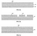
- FIG. 1shows a process flow of a typical state of the art MEMS structure manufacturing process including a packaging step.
- a silicon substrate 10 carrying an oxide layer 12 and a patterned silicon layer 14 including resonant structures 16is provided.
- the resonator trenchesare resealed with oxide 18, which is etched to provide contact regions to the underlying silicon layer 14.
- a thin (e.g. 2 micron) layer 20 of siliconis deposited over the substrate stack in which micron-scale vent channels (not shown) are etched to allow HF vapor access for release of the resonant structures 16 in step (d), in which the cavities 22 each including a resonant structure 16 are formed.
- step (e)a silicon encapsulation layer 24 is deposited at 950°C followed by a CMP planarization and etching of the encapsulation layer 24 to define the electrical contacts.
- step (f)oxide 26 is deposited to seal the trenches and is etched to allow the electrical contact to the underlying encapsulation layer 24, after which aluminum contacts 28 are formed in step (g) by deposition and etching.
- vent channelsrequire an additional processing step, thus adding to the cost of the overall manufacturing process.
- the vent channelsshould not be located directly over the cavity, thus limiting the flexibility of the manufacturing process.
- relatively thick capping layersare required to effectively seal the cavity, thus further adding to the cost of the manufacturing process.
- the capping materialconsists of a low temperature PECVD layer of SiOC (trade name Black Diamond) and is shown to be permeable to HF vapor and H 2 O and therefore allows for the removal of a SiO 2 sacrificial layer and the formation of a cavity underneath the capping layer, with the capping material being permeable enough to allow for the evacuation of the SiO 2 reaction products.
- the cavity underneath the capping layerallows for high-Q operation of a MEMS resonator.
- a sealing layercan be deposited on the capping layer without significantly contaminating the cavity. However, it has been found that residual contamination of the cavity is difficult to avoid, especially when a sealing layer consisting of relatively small molecules is formed. In addition, there are no suitable process steps available to seal the porous layer at high temperature and low pressure, such that it is difficult to obtain a cavity with a high quality vacuum using this method.
- a porous polysilicon cap layeris obtained over a MEMS structure by electrochemical etching of a polysilicon layer. Sealing of this layer is performed with the deposition of a further polysilicon layer or an LPCVD silicon oxide layer.
- the drawback of this approachis that the electrochemical etching of the polysilicon layer to obtain the porous polysilicon cannot be readily achieved in standard manufacturing tools, thus requiring an additional investment.
- the packaging method proposed in this paperrequires the inclusion of a critical point drying step after the cavity formation for avoiding the MEMS structures sticking to the cavity walls. Furthermore, the required background pressures of the proposed sealing techniques are such that the preferable low pressure in the packaged cavity cannot be achieved.
- US2009/0145976 A1describes the packaging of micro devices.
- a thin layer of metalis deposited and etched to form device metallization, including electrodes and bondpads.
- a passivation layer of silicon nitrideis patterned to open access points to the metal.
- a lower sacrificial layeris formed from polyimide and is patterned to open anchor regions for a device and for bridges that will define lateral etch channels for package evacuation.
- Structural materials that form a MEMS device and bridgesare then deposited and patterned. The bridges are patterned simultaneously with the device on the lower sacrificial layer.
- An upper sacrificial layeris then deposited over the device and the lower sacrificial layer and is patterned to open anchor regions for an encapsulation layer.
- Both sacrificial layersare then simultaneously removed in an oxygen plasma ash through lateral etc channels. This step leaves a hollow and empty shell, inside which the MEMS device is present. The device is free to move after sacrificial layer removal and has clearance both above and below.
- the etch channelsare sealed by a sealant applied over the encapsulant layer.
- US 2009/194309 A1discloses a method for packaging a MEMs element comprising: encapsulating a MEMS element with a sacrificial layer portion of a sacrificial material deposited over a substrate arrangement, said portion defining a cavity for the MEMS; forming at least one strip of a further sacrificial material extending outwardly from said portion; forming a cover layer portion over the sacrificial layer portion; removing the sacrificial layer portion and the at least one strip, the removal of the at least one strip defining at least one vent channel extending laterally underneath the cover layer portion; and sealing the at least one vent channel.
- the cover layer portioncovers the entire strip, except for an etch hole.
- the present inventionseeks to provide a cost-effective method of packaging a MEMS structure, preferably in a low pressure cavity on a substrate.
- the present inventionfurther seeks to provide a device comprising such a packaged MEMS structure.
- a forming a MEMS devicecomprising encapsulating a MEMS element with a sacrificial layer portion deposited over a substrate arrangement, said portion defining a cavity for the MEMS element; forming at least one strip of a further sacrificial material extending outwardly from said portion; forming a cover layer portion over the sacrificial layer portion, said cover layer portion terminating on the at least one strip; removing the sacrificial layer portion and the at least one strip, the removal of the at least one strip defining at least one vent channel extending laterally underneath the cover layer portion; and sealing the at least one vent channel.
- the present inventionhas been based on the insight that lateral vent channels can be formed that extend from the cavity to be formed in a lateral direction underneath the cover of the cavity, such that upon sealing of the vent channels, contamination of the cavity can be avoided.
- the channelsare preferably kept very small, i.e. by providing one or more strips with a thickness in the range of 5-50 nm to prevent significant contamination of the cavity and to allow for the vent channels to be effectively sealed in the sealing step.
- the above embodiment of the present inventionis particularly suitable for the formation of relatively small cavities.
- etchinge.g. a hydrogen fluoride (HF) etch
- the etch duration required to fully remove the sacrificial layer portioncan cause damage to other parts of the device.
- the cover layer portioninto a porous cover layer portion by chemical treatment of the cover layer portion, said chemical treatment simultaneously removing the sacrificial layer portion and the at least one strip such that the removal of the sacrificial layer portion can mainly take place through the porous cover layer portion, thereby reducing the time it takes to form the cavity, such that other components of the device are less likely to be damaged during the removal of the sacrificial layer portion.
- vent channelswhen a material is used that can be converted into a porous material by such chemical treatment the presence of the vent channels becomes superfluous.
- the material made porous by the chemical treatmentcan become very reactive, such that upon completion of the chemical treatment the porous material immediately seals again by reaction with ambient reactants such as water and air, which can cause residual gases to become trapped inside the cavity, which makes it difficult to set the pressure inside the cavity to the desired value.
- the presence of the vent channelsensures that such residual gases can still escape from the cavity upon completion of the chemical treatment step.
- the cover layer portioncomprises SIPOS (semi-insulating polycrystalline silicon), and wherein said chemical treatment step comprises treating the SIPOS with a hydrogen fluoride (HF) etch recipe, as SIPOS may be temporarily made porous by treatment with HF, which furthermore is a suitable etchant for removing sacrificial materials such as silicon oxide (SiO 2 ) and TEOS (tetraethyl-orthosilicate).
- SIPOShydrogen fluoride
- HFhydrogen fluoride
- the methodfurther comprises forming a patterned support layer over the sacrificial layer portion, said patterned support layer defining etching holes on top of the sacrificial layer portion, wherein the step of forming the cover layer portion comprises forming the cover layer portion over the sacrificial layer portion including the patterned support layer, and wherein the cover layer portion is separated from the at least one strip by a portion of the patterned support layer.
- the support layerpreferably is a polysilicon layer.
- the sealing stepcomprises depositing a capping layer over the resultant structure, which may be performed at a vacuum pressure, e.g. in the range of 10 -4 - 10 -6 Torr to ensure that the pressure inside the cavity is set to the desired (near-)vacuum pressure.
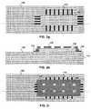
- a substrate 100which may be any suitable substrate, e.g. a silicon substrate, a silicon-on-insulator (SOI) substrate, a SiGe substrate and so on, is provided with a first layer 110 of a sacrificial material, onto which a layer of a suitable material 120, e.g. silicon, is deposited and subsequently patterned, e.g. by means of wet chemical etching or reactive ion etching (RIE) to form the outline of MEMS structure 122, such as a MEMS resonator or another suitable MEMS device as shown in FIG 2b .
- RIEreactive ion etching
- the patterning stepshould be selective to the underlying sacrificial layer 110 if present. Such processing steps are well-known to the skilled person and will not be explained in further detail for reasons of brevity only.
- Any suitable sacrificial materialmay be used.
- suitable sacrificial materialsinclude TEOS (tetraethyl-orthosilicate) and SiO 2 , e.g. a LPCVD (low-pressure chemical vapor deposition) silicon dioxide.
- the sacrificial material layer 110may be omitted in case the MEMS device 122 is to be anchored on the substrate 100. After patterning of layer 120 to form the MEMS device 122, ion implantations into the layer 120 may be performed if necessary.
- a layer 130 of a further sacrificial materialis deposited over the patterned material layer 120 such that the MEMS device 122 is fully covered by the sacrificial material in the cross-section of the device shown in FIG. 2 .
- the sacrificial layer 130is of a material that can be removed in the same process step as the removal of the material of the optional sacrificial layer 110.
- the material of the sacrificial layer 130may be the same as the material of the sacrificial layer 110.
- the further sacrificial layer 130is patterned in any suitable manner, e.g. by photolithography and subsequent etching, such as wet chemical etching or RIE, thereby forming a portion of the sacrificial layer 130 that covers the MEMS device 122 and defines at least part of the cavity to be formed around the MEMS device 122.
- the remainder of the cavity to be formedmay be defined by a portion of the sacrificial layer 110.
- the patterning of the further sacrificial layer 130preferably is performed by an etching step that is selective to the underlying layer 120, e.g. a silicon layer.
- the methodproceeds as shown in FIG. 2e with the growth or deposition of a second further sacrificial layer 132, e.g. a TEOS or SiO 2 layer over the resultant structure.
- the second further sacrificial layer 132is preferably much thinner than the further sacrificial layer 130, e.g. in the range of 5-50 nm compared to a typical thickness of the further sacrificial layer 130 in the micrometer domain.
- the further sacrificial layer 130preferably has a thickness ranging from a few hundred nanometer to several micrometer as it has been found that a further sacrificial layer 130 having a thickness in this range is sufficiently thick to prevent sticking of the cap layer 135 to the MEMS device 122 during its release, whilst being thin enough to avoid complications in the further processing of the MEMS device 122.
- the second further sacrificial layer 132is subsequently patterned as shown in FIG. 2f in any suitable manner, e.g. using photolithography followed by an etching step such as a wet chemical etching step or a RIE step to form at least one strip of the second further sacrificial layer 132 that lies against the portion of the further sacrificial layer 130 covering the MEMS device 122, with one or more strips of the second further sacrificial layer 132 extending laterally from this portion.
- a top view of this structureis shown in FIG. 2g .
- the strips 132will act as vent channels for the degassing of the cavity of the MEMS device 122 as will be explained in more detail later.
- the number of strips 132may be determined by the desired degassing rate, with higher rates requiring more strips 132. However, it should be understood that in principle a single strip 132 may suffice, in particular when the volume of the cavity to be formed is relatively small.
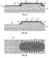
- the methodmay proceed as shown in FIG. 2h with the deposition and subsequent patterning of a support layer 135, which is intended to strengthen the lid of the cavity to be formed against collapsing.
- a support layer 135Any suitable material may be used for the support layer 135, such as polycrystalline silicon (poly-Si).
- the patterning of the support layer 135may be achieved in any suitable manner, e.g. by etching, which etching step should be selective to the underlying further sacrificial layer 130 and the second further sacrificial layer 132.
- the patterning of the support layer 135may optionally include the formation of etch holes on top of the portion of the underlying further sacrificial layer 130 covering the MEMS device 122.
- FIG. 2iA top view of the resultant structure after the patterning of the support layer 135 is shown in FIG. 2i , which includes the etch holes exposing the underlying portion of the further sacrificial layer 130.
- the formation of the support layer 135is omitted from the method of the present invention, such that the method proceeds from the step shown in FIG. 2f directly to the step shown in FIG. 2j .
- the presence of the support layer 135is however preferred as it strengthens the cavity of the MEMS device 122 as previously explained.
- the methodproceeds as shown in FIG. 2j , in which a cover layer 140 is formed over the resultant structure.
- the cover layer 140is subsequently patterned as shown in FIG. 2k , such that the cover layer 140 covers the portion of the further sacrificial layer 130 that covers the MEMS device 122 and the patterned support layer 135 if present.
- the patterning of the cover layer 140ensures that the end portions of the strips 132 are exposed, i.e. that the cover layer 140 terminates on the strips 132.
- a portion of the patterned cover layer 140 over a strip 132may be separated from the strip 132 by a portion of the patterned support layer 135.
- a top view of the resulting structureis shown in FIG. 2I .
- the cover layer 140may be a permanently non-porous layer, in which case the subsequent removal of the sacrificial materials, e.g. materials 110, 130 and 132 is to be achieved through vent channels to be formed by the removal of the strips 132. This may be a feasible embodiment if the cavity to be formed is small enough such that the complete removal of the respective sacrificial materials may be achieved quickly enough such that other parts of the device are not damaged by the chemicals used for the removal of these sacrificial materials.
- the cover layer 140comprises a material that can be made porous by chemical treatment such that the removal of the sacrificial materials for defining the MEMS cavity and the vent channels can also take place through the pores of the material of the cover layer 140.
- a preferred embodiment of such a materialis SIPOS, which is an oxide-rich poly-Si, which may be formed by the co-deposition of SiO 2 and silicon or by depositing poly-Si in a (slightly) oxidizing atmosphere.
- the SIPOS layer 140may be patterned in any suitable manner, e.g. by means of a wet chemical etch or by means of a RIE step.
- FIG. 2mshows an alternative embodiment of FIG. 2k , in which the cover layer 140 is patterned simultaneously with the support layer 135, i.e. both layers are patterned by a single patterning step such as a wet chemical etch or a RIE step.
- a single patterning stepsuch as a wet chemical etch or a RIE step.
- the support layer 135should further comprise etch windows on top of the portion of the further sacrificial layer 130 that covers the MEMS device 122, these etch windows should be formed prior to the deposition of the cover layer 140.
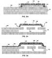
- the methodsubsequently proceeds from the resultant structure shown in FIG. 2k or from the resultant structure shown in FIG 2m as shown in FIG. 2n , in which the MEMS device 122 is released from the substrate 100 by the simultaneous removal of the sacrificial materials, e.g. a portion of the sacrificial layer 110 if present, the portion of the further sacrificial layer 130 and the one or more strips formed by the patterning of the second further sacrificial layer 132, thereby forming a cavity 150.
- the sacrificial materialse.g. a portion of the sacrificial layer 110 if present
- the portion of the further sacrificial layer 130 and the one or more strips formed by the patterning of the second further sacrificial layer 132thereby forming a cavity 150.
- the cover layer 140is a SIPOS layer, in which case the removal of the sacrificial materials is performed by HF etching, which simultaneously removes an SiO x component (0 ⁇ x ⁇ 2) from the SIPOS cover layer 140, thereby rendering the SIPOS cover layer 140 porous, such that the removal of the sacrificial materials is mainly achieved through the porous SIPOS cover layer 140.
- the exposure to the etch recipe, e.g. the HF etch recipeshould be long enough to ensure that the strips 132 are fully removed, thereby forming the vent channels 134 laterally extending from the cavity 150 to the outside world.
- the vent channels 134are formed between the material layer 120 and a portion of cover layer 140 or a portion of the support layer 135 if present.
- the height of the vent channels 134i.e. the distance between the material layer 120 and the opposite portion of cover layer 140 or the portion of the support layer 135 if present preferably lies in the range of 5-50 nm. Below 5 nm degassing through the vent channels 134 becomes cumbersome, and above 50 nm the subsequent sealing of the vent channels 134 becomes cumbersome.
- the porous SIPOS cover layer 140will rapidly react with ambient reactants, e.g. water or air, which will effectively seal the SIPOS layer 140.
- the methodnext proceeds to step 2o, in which a sealing or capping layer 160 is deposited over the resultant structure to seal the cover layer 140 if necessary but more importantly to seal the vent channels 134.
- the sealing layer 160preferably is an electrically insulating layer. Suitable materials for the sealing layer 160 include SiO x (0 ⁇ x ⁇ 2) and Al 2 O 3 .
- the sealing layer 160may be deposited in any suitable manner, e.g. by physical vapor deposition. In a preferred embodiment, the deposition is performed at a near-vacuum pressure, e.g.
- the methodmay further include post-packaging processing steps, such as the formation, e.g. etching, of a contact region for the MEMS structure 122 through the sealing layer 160 to the underlying material layer 120, as shown in FIG. 2p , after which a conductive contact 180 may be formed in the contact region as shown in FIG. 2q .
- the conductive contact 180may be a metal contact, e.g. an Al contact, and may be formed in any suitable manner, e.g. by depositing a metal layer over the resultant structure of FIG. 2p and patterning this layer to form the metal contact. Alternatively, a selective deposition process may be used.
Landscapes
- Engineering & Computer Science (AREA)
- Microelectronics & Electronic Packaging (AREA)
- Manufacturing & Machinery (AREA)
- Micromachines (AREA)
Description
- The present invention relates to a method of forming a MEMS device.
- The present invention further related to a device comprising such a MEMS structure.
- The ongoing miniaturization of feature sizes in semiconductor manufacturing processes has facilitated the formation of microscopic structures, i.e. structures that have feature sizes in the micron and submicron, e.g. nanometer domain, on substrates such as silicon substrates. A prime example of such a microscopic structure is a microelectromechanical system (MEMS) structure. Such structures are sometimes also referred to as micromachines.
- MEMS structures can be used for a wide range of applications in different fields of technology, e.g. electronics, medicine, pharmacy and chemistry. Applications in the filed of electronics for instance include accelerometers, gyroscopes, sensors, and so on. The MEMS structures may be made from any suitable material, e.g. silicon, polymer, metals amongst others.
- Typically, the MEMS structure requires a certain degree of translational freedom in order to perform its function. To this end, the MEMS structure is packaged such that the structure is located in a sealed cavity.
FIG. 1 shows a process flow of a typical state of the art MEMS structure manufacturing process including a packaging step. In step (a), asilicon substrate 10 carrying anoxide layer 12 and a patternedsilicon layer 14 includingresonant structures 16 is provided. In step (b), the resonator trenches are resealed withoxide 18, which is etched to provide contact regions to the underlyingsilicon layer 14. In step (c), a thin (e.g. 2 micron)layer 20 of silicon is deposited over the substrate stack in which micron-scale vent channels (not shown) are etched to allow HF vapor access for release of theresonant structures 16 in step (d), in which thecavities 22 each including aresonant structure 16 are formed. In step (e), asilicon encapsulation layer 24 is deposited at 950°C followed by a CMP planarization and etching of theencapsulation layer 24 to define the electrical contacts. In step (f),oxide 26 is deposited to seal the trenches and is etched to allow the electrical contact to theunderlying encapsulation layer 24, after whichaluminum contacts 28 are formed in step (g) by deposition and etching.- This process flow has several drawbacks. For instance, the etching of the micrometer sized vent channels requires an additional processing step, thus adding to the cost of the overall manufacturing process. Also, to avoid contamination of the cavity containing the MEMS structure with capping material, the vent channels should not be located directly over the cavity, thus limiting the flexibility of the manufacturing process. Moreover, relatively thick capping layers are required to effectively seal the cavity, thus further adding to the cost of the manufacturing process.
- In the paper "Wafer Level Encapsulation Technology for MEMS Devices using a HF-Permeable PECVD SIOC Capping Layer" by G.J.A.M. Verheijden et al. in MEMS 2008, IEEE 21st conference on Micro Electro Mechanical Systems 2008, pages 798-801, an alternative technology for the encapsulation of MEMS devices using a porous capping material is disclosed, which overcomes many of the problems associated with the process of
FIG. 1 . - The capping material consists of a low temperature PECVD layer of SiOC (trade name Black Diamond) and is shown to be permeable to HF vapor and H2O and therefore allows for the removal of a SiO2 sacrificial layer and the formation of a cavity underneath the capping layer, with the capping material being permeable enough to allow for the evacuation of the SiO2 reaction products. The cavity underneath the capping layer allows for high-Q operation of a MEMS resonator. A sealing layer can be deposited on the capping layer without significantly contaminating the cavity. However, it has been found that residual contamination of the cavity is difficult to avoid, especially when a sealing layer consisting of relatively small molecules is formed. In addition, there are no suitable process steps available to seal the porous layer at high temperature and low pressure, such that it is difficult to obtain a cavity with a high quality vacuum using this method.
- InR. He et al, Journal of Micro-electromechanical Systems, Vol. 16, pages 462-472 (2007), a porous polysilicon cap layer is obtained over a MEMS structure by electrochemical etching of a polysilicon layer. Sealing of this layer is performed with the deposition of a further polysilicon layer or an LPCVD silicon oxide layer. The drawback of this approach is that the electrochemical etching of the polysilicon layer to obtain the porous polysilicon cannot be readily achieved in standard manufacturing tools, thus requiring an additional investment. In addition, the packaging method proposed in this paper requires the inclusion of a critical point drying step after the cavity formation for avoiding the MEMS structures sticking to the cavity walls. Furthermore, the required background pressures of the proposed sealing techniques are such that the preferable low pressure in the packaged cavity cannot be achieved.
US2009/0145976 A1 describes the packaging of micro devices. A thin layer of metal is deposited and etched to form device metallization, including electrodes and bondpads. A passivation layer of silicon nitride is patterned to open access points to the metal. A lower sacrificial layer is formed from polyimide and is patterned to open anchor regions for a device and for bridges that will define lateral etch channels for package evacuation. Structural materials that form a MEMS device and bridges are then deposited and patterned. The bridges are patterned simultaneously with the device on the lower sacrificial layer. An upper sacrificial layer is then deposited over the device and the lower sacrificial layer and is patterned to open anchor regions for an encapsulation layer. Both sacrificial layers are then simultaneously removed in an oxygen plasma ash through lateral etc channels. This step leaves a hollow and empty shell, inside which the MEMS device is present. The device is free to move after sacrificial layer removal and has clearance both above and below. The etch channels are sealed by a sealant applied over the encapsulant layer.US 2009/194309 A1 discloses a method for packaging a MEMs element comprising: encapsulating a MEMS element with a sacrificial layer portion of a sacrificial material deposited over a substrate arrangement, said portion defining a cavity for the MEMS; forming at least one strip of a further sacrificial material extending outwardly from said portion; forming a cover layer portion over the sacrificial layer portion; removing the sacrificial layer portion and the at least one strip, the removal of the at least one strip defining at least one vent channel extending laterally underneath the cover layer portion; and sealing the at least one vent channel. The cover layer portion covers the entire strip, except for an etch hole.- The present invention seeks to provide a cost-effective method of packaging a MEMS structure, preferably in a low pressure cavity on a substrate.
- The present invention further seeks to provide a device comprising such a packaged MEMS structure.
- Aspects of the invention are defined in the accompanying claims.
- In accordance with a first aspect of the present invention, there is provided a forming a MEMS device, comprising encapsulating a MEMS element with a sacrificial layer portion deposited over a substrate arrangement, said portion defining a cavity for the MEMS element; forming at least one strip of a further sacrificial material extending outwardly from said portion; forming a cover layer portion over the sacrificial layer portion, said cover layer portion terminating on the at least one strip; removing the sacrificial layer portion and the at least one strip, the removal of the at least one strip defining at least one vent channel extending laterally underneath the cover layer portion; and sealing the at least one vent channel.
- The present invention has been based on the insight that lateral vent channels can be formed that extend from the cavity to be formed in a lateral direction underneath the cover of the cavity, such that upon sealing of the vent channels, contamination of the cavity can be avoided. The channels are preferably kept very small, i.e. by providing one or more strips with a thickness in the range of 5-50 nm to prevent significant contamination of the cavity and to allow for the vent channels to be effectively sealed in the sealing step.
- It is noted that the above embodiment of the present invention is particularly suitable for the formation of relatively small cavities. For larger cavities, if the sacrificial materials are to be removed by etching, e.g. a hydrogen fluoride (HF) etch, the etch duration required to fully remove the sacrificial layer portion can cause damage to other parts of the device.
- For larger cavities, it is advantageous to convert the cover layer portion into a porous cover layer portion by chemical treatment of the cover layer portion, said chemical treatment simultaneously removing the sacrificial layer portion and the at least one strip such that the removal of the sacrificial layer portion can mainly take place through the porous cover layer portion, thereby reducing the time it takes to form the cavity, such that other components of the device are less likely to be damaged during the removal of the sacrificial layer portion.
- It may appear that when a material is used that can be converted into a porous material by such chemical treatment the presence of the vent channels becomes superfluous. However, it has been surprisingly found by the present invention that this is not the case. This is because the material made porous by the chemical treatment can become very reactive, such that upon completion of the chemical treatment the porous material immediately seals again by reaction with ambient reactants such as water and air, which can cause residual gases to become trapped inside the cavity, which makes it difficult to set the pressure inside the cavity to the desired value. The presence of the vent channels ensures that such residual gases can still escape from the cavity upon completion of the chemical treatment step.
- In a preferred embodiment, the cover layer portion comprises SIPOS (semi-insulating polycrystalline silicon), and wherein said chemical treatment step comprises treating the SIPOS with a hydrogen fluoride (HF) etch recipe, as SIPOS may be temporarily made porous by treatment with HF, which furthermore is a suitable etchant for removing sacrificial materials such as silicon oxide (SiO2) and TEOS (tetraethyl-orthosilicate).
- In an embodiment, the method further comprises forming a patterned support layer over the sacrificial layer portion, said patterned support layer defining etching holes on top of the sacrificial layer portion, wherein the step of forming the cover layer portion comprises forming the cover layer portion over the sacrificial layer portion including the patterned support layer, and wherein the cover layer portion is separated from the at least one strip by a portion of the patterned support layer. This has the advantage of improving the structural integrity of the cavity as well as defining etch holes on top of the sacrificial layer portion and defining the length of the vent channels to be formed. The support layer preferably is a polysilicon layer.
- In an embodiment, the sealing step comprises depositing a capping layer over the resultant structure, which may be performed at a vacuum pressure, e.g. in the range of 10-4 - 10-6 Torr to ensure that the pressure inside the cavity is set to the desired (near-)vacuum pressure.
- Embodiments of the invention are described in more detail and by way of non-limiting examples with reference to the accompanying drawings, wherein:
Figs. 1a-g depict a known method of manufacturing a MEMS device; andFigs. 2a-q depict a method of manufacturing a MEMS device in accordance with an exemplary embodiment of the present invention.- It should be understood that the Figures are merely schematic and are not drawn to scale. It should also be understood that the same reference numerals are used throughout the Figures to indicate the same or similar parts.
- A first embodiment of a packaging method of the present invention is described in more detail with the aid of
FIG. 2 . InFIG. 2a , asubstrate 100, which may be any suitable substrate, e.g. a silicon substrate, a silicon-on-insulator (SOI) substrate, a SiGe substrate and so on, is provided with afirst layer 110 of a sacrificial material, onto which a layer of asuitable material 120, e.g. silicon, is deposited and subsequently patterned, e.g. by means of wet chemical etching or reactive ion etching (RIE) to form the outline ofMEMS structure 122, such as a MEMS resonator or another suitable MEMS device as shown inFIG 2b . The patterning step should be selective to the underlyingsacrificial layer 110 if present. Such processing steps are well-known to the skilled person and will not be explained in further detail for reasons of brevity only. Any suitable sacrificial material may be used. Non-limiting examples of suitable sacrificial materials include TEOS (tetraethyl-orthosilicate) and SiO2, e.g. a LPCVD (low-pressure chemical vapor deposition) silicon dioxide. In an alternative embodiment, thesacrificial material layer 110 may be omitted in case theMEMS device 122 is to be anchored on thesubstrate 100. After patterning oflayer 120 to form theMEMS device 122, ion implantations into thelayer 120 may be performed if necessary. - In
FIG. 2c , alayer 130 of a further sacrificial material is deposited over the patternedmaterial layer 120 such that theMEMS device 122 is fully covered by the sacrificial material in the cross-section of the device shown inFIG. 2 . In a preferred embodiment, thesacrificial layer 130 is of a material that can be removed in the same process step as the removal of the material of the optionalsacrificial layer 110. For instance, the material of thesacrificial layer 130 may be the same as the material of thesacrificial layer 110. - In
FIG. 2d , the furthersacrificial layer 130 is patterned in any suitable manner, e.g. by photolithography and subsequent etching, such as wet chemical etching or RIE, thereby forming a portion of thesacrificial layer 130 that covers theMEMS device 122 and defines at least part of the cavity to be formed around theMEMS device 122. The remainder of the cavity to be formed may be defined by a portion of thesacrificial layer 110. The patterning of the furthersacrificial layer 130 preferably is performed by an etching step that is selective to theunderlying layer 120, e.g. a silicon layer. - The method proceeds as shown in
FIG. 2e with the growth or deposition of a second furthersacrificial layer 132, e.g. a TEOS or SiO2 layer over the resultant structure. The second furthersacrificial layer 132 is preferably much thinner than the furthersacrificial layer 130, e.g. in the range of 5-50 nm compared to a typical thickness of the furthersacrificial layer 130 in the micrometer domain. The furthersacrificial layer 130 preferably has a thickness ranging from a few hundred nanometer to several micrometer as it has been found that a furthersacrificial layer 130 having a thickness in this range is sufficiently thick to prevent sticking of thecap layer 135 to theMEMS device 122 during its release, whilst being thin enough to avoid complications in the further processing of theMEMS device 122. - The second further
sacrificial layer 132 is subsequently patterned as shown inFIG. 2f in any suitable manner, e.g. using photolithography followed by an etching step such as a wet chemical etching step or a RIE step to form at least one strip of the second furthersacrificial layer 132 that lies against the portion of the furthersacrificial layer 130 covering theMEMS device 122, with one or more strips of the second furthersacrificial layer 132 extending laterally from this portion. A top view of this structure is shown inFIG. 2g . Thestrips 132 will act as vent channels for the degassing of the cavity of theMEMS device 122 as will be explained in more detail later. The number ofstrips 132 may be determined by the desired degassing rate, with higher rates requiring more strips 132. However, it should be understood that in principle asingle strip 132 may suffice, in particular when the volume of the cavity to be formed is relatively small. - The method may proceed as shown in
FIG. 2h with the deposition and subsequent patterning of asupport layer 135, which is intended to strengthen the lid of the cavity to be formed against collapsing. Any suitable material may be used for thesupport layer 135, such as polycrystalline silicon (poly-Si). The patterning of thesupport layer 135 may be achieved in any suitable manner, e.g. by etching, which etching step should be selective to the underlying furthersacrificial layer 130 and the second furthersacrificial layer 132. The patterning of thesupport layer 135 may optionally include the formation of etch holes on top of the portion of the underlying furthersacrificial layer 130 covering theMEMS device 122. This optional embodiment is for instance useful if a cover layer to be formed is to be made porous to assist the degassing of the cavity to be formed, as will be explained in more detail later. A top view of the resultant structure after the patterning of thesupport layer 135 is shown inFIG. 2i , which includes the etch holes exposing the underlying portion of the furthersacrificial layer 130. - It is noted that in an alternative embodiment, the formation of the
support layer 135 is omitted from the method of the present invention, such that the method proceeds from the step shown inFIG. 2f directly to the step shown inFIG. 2j . The presence of thesupport layer 135 is however preferred as it strengthens the cavity of theMEMS device 122 as previously explained. - The method proceeds as shown in
FIG. 2j , in which acover layer 140 is formed over the resultant structure. Thecover layer 140 is subsequently patterned as shown inFIG. 2k , such that thecover layer 140 covers the portion of the furthersacrificial layer 130 that covers theMEMS device 122 and the patternedsupport layer 135 if present. In addition, the patterning of thecover layer 140 ensures that the end portions of thestrips 132 are exposed, i.e. that thecover layer 140 terminates on thestrips 132. In case of the presence of the patternedsupport layer 135, a portion of the patternedcover layer 140 over astrip 132 may be separated from thestrip 132 by a portion of the patternedsupport layer 135. A top view of the resulting structure is shown inFIG. 2I . - The
cover layer 140 may be a permanently non-porous layer, in which case the subsequent removal of the sacrificial materials,e.g. materials strips 132. This may be a feasible embodiment if the cavity to be formed is small enough such that the complete removal of the respective sacrificial materials may be achieved quickly enough such that other parts of the device are not damaged by the chemicals used for the removal of these sacrificial materials. - In a preferred embodiment, the
cover layer 140 comprises a material that can be made porous by chemical treatment such that the removal of the sacrificial materials for defining the MEMS cavity and the vent channels can also take place through the pores of the material of thecover layer 140. A preferred embodiment of such a material is SIPOS, which is an oxide-rich poly-Si, which may be formed by the co-deposition of SiO2 and silicon or by depositing poly-Si in a (slightly) oxidizing atmosphere. TheSIPOS layer 140 may be patterned in any suitable manner, e.g. by means of a wet chemical etch or by means of a RIE step. FIG. 2m shows an alternative embodiment ofFIG. 2k , in which thecover layer 140 is patterned simultaneously with thesupport layer 135, i.e. both layers are patterned by a single patterning step such as a wet chemical etch or a RIE step. This leads to a subsequently vertical structure on the one ormore strips 132, said vertical structure formed by a portion of the patternedsupport layer 135 and a portion of thecover layer 140. In this embodiment, if thesupport layer 135 should further comprise etch windows on top of the portion of the furthersacrificial layer 130 that covers theMEMS device 122, these etch windows should be formed prior to the deposition of thecover layer 140.- The method subsequently proceeds from the resultant structure shown in
FIG. 2k or from the resultant structure shown inFIG 2m as shown inFIG. 2n , in which theMEMS device 122 is released from thesubstrate 100 by the simultaneous removal of the sacrificial materials, e.g. a portion of thesacrificial layer 110 if present, the portion of the furthersacrificial layer 130 and the one or more strips formed by the patterning of the second furthersacrificial layer 132, thereby forming acavity 150. As previously mentioned, in a preferred embodiment, thecover layer 140 is a SIPOS layer, in which case the removal of the sacrificial materials is performed by HF etching, which simultaneously removes an SiOx component (0<x≤2) from theSIPOS cover layer 140, thereby rendering theSIPOS cover layer 140 porous, such that the removal of the sacrificial materials is mainly achieved through the porousSIPOS cover layer 140. The exposure to the etch recipe, e.g. the HF etch recipe should be long enough to ensure that thestrips 132 are fully removed, thereby forming thevent channels 134 laterally extending from thecavity 150 to the outside world. Thevent channels 134 are formed between thematerial layer 120 and a portion ofcover layer 140 or a portion of thesupport layer 135 if present. The height of thevent channels 134, i.e. the distance between thematerial layer 120 and the opposite portion ofcover layer 140 or the portion of thesupport layer 135 if present preferably lies in the range of 5-50 nm. Below 5 nm degassing through thevent channels 134 becomes cumbersome, and above 50 nm the subsequent sealing of thevent channels 134 becomes cumbersome. - Following the termination of the etch step, the porous
SIPOS cover layer 140 will rapidly react with ambient reactants, e.g. water or air, which will effectively seal theSIPOS layer 140. The method next proceeds to step 2o, in which a sealing orcapping layer 160 is deposited over the resultant structure to seal thecover layer 140 if necessary but more importantly to seal thevent channels 134. Thesealing layer 160 preferably is an electrically insulating layer. Suitable materials for thesealing layer 160 include SiOx (0<x≤2) and Al2O3. Thesealing layer 160 may be deposited in any suitable manner, e.g. by physical vapor deposition. In a preferred embodiment, the deposition is performed at a near-vacuum pressure, e.g. a pressure in the range of 10-4-10-6 Torr (mm Hg). This ensures that the pressure in thecavity 150 is set to the operating pressure of the deposition process, as any overpressure in thecavity 150 can escape through the one ormore vent channels 134 prior to the effective sealing of these channels. Upon sealing of thevent channels 134, thecavity 150 has become hermetically sealed. - The method may further include post-packaging processing steps, such as the formation, e.g. etching, of a contact region for the
MEMS structure 122 through thesealing layer 160 to theunderlying material layer 120, as shown inFIG. 2p , after which aconductive contact 180 may be formed in the contact region as shown inFIG. 2q . Theconductive contact 180 may be a metal contact, e.g. an Al contact, and may be formed in any suitable manner, e.g. by depositing a metal layer over the resultant structure ofFIG. 2p and patterning this layer to form the metal contact. Alternatively, a selective deposition process may be used. - It should be noted that the above-mentioned embodiments illustrate rather than limit the invention, and that those skilled in the art will be able to design many alternative embodiments without departing from the scope of the appended claims. In the claims, any reference signs placed between parentheses shall not be construed as limiting the claim. The word "comprising" does not exclude the presence of elements or steps other than those listed in a claim. The word "a" or "an" preceding an element does not exclude the presence of a plurality of such elements. In the device claim enumerating several means, several of these means can be embodied by one and the same item of hardware. The mere fact that certain measures are recited in mutually different dependent claims does not indicate that a combination of these measures cannot be used to advantage.
Claims (10)
- A method of forming a MEMS device, comprising:encapsulating a MEMS element (122) with a first layer (110) of a sacrificial material and a further sacrificial layer portion (130) of the sacrificial material deposited over a substrate arrangement (100), said portion defining a cavity (150) for the MEMS element;forming at least one strip (132) of a further sacrificial material extending outwardly from said portion;forming a cover layer portion (140) over the sacrificial layer portion, said cover layer portion terminating on the at least one strip;removing the sacrificial layer portion and the at least one strip, the removal of the at least one strip defining at least one vent channel (134) extending laterally underneath the cover layer portion; andsealing the at least one vent channel.
- The method of claim 1, wherein the step of forming at least one strip (132) of a further sacrificial material comprises forming a plurality of said strips.
- The method of claim 1 or 2, further comprising converting the cover layer portion (140) into a porous cover layer portion by chemically treatment of the cover layer portion, said chemically treatment simultaneously removing the sacrificial layer portion (130) and the at least one strip (132).
- The method of claim 3, wherein cover layer portion (140) comprises SIPOS (semi-insulating polycrystalline silicon), and wherein said chemically treatment step comprises treating the SIPOS with a hydrogen fluoride etch recipe.
- The method of any of claims 1-4, wherein the thickness of the at least one strip (132) is in the range of 5-50 nm.
- The method of any of claims 1-5, further comprising forming a patterned support layer (135) over the sacrificial layer portion (130), said patterned support layer defining etching holes on top of the sacrificial layer portion, wherein the step of forming the cover layer portion (140) comprises forming the cover layer portion over the sacrificial layer portion including the patterned support layer, and wherein the cover layer portion is separated from the at least one strip (132) by a portion of the patterned support layer.
- The method of claim 6, wherein the patterned support layer (135) is a polysilicon layer.
- The method of any of claims 1-7, wherein said sealing step comprises depositing a capping layer (160) over the resultant structure.
- The method of claim 8, wherein said deposition step is performed at a vacuum pressure.
- The method of any of claims 1-9, wherein the sacrificial layer portion (130) and the at least one strip (132) are removed by hydrogen fluoride etching.
Priority Applications (3)
| Application Number | Priority Date | Filing Date | Title |
|---|---|---|---|
| EP10195471.7AEP2465817B1 (en) | 2010-12-16 | 2010-12-16 | Method for encapsulating a MEMS structure |
| CN201110415082.2ACN102556946B (en) | 2010-12-16 | 2011-12-13 | Method for encapsulating a MEMS structure and encapsulated MEMS structure |
| US13/325,320US8766380B2 (en) | 2010-12-16 | 2011-12-14 | MEMS device forming method and device with MEMS structure |
Applications Claiming Priority (1)
| Application Number | Priority Date | Filing Date | Title |
|---|---|---|---|
| EP10195471.7AEP2465817B1 (en) | 2010-12-16 | 2010-12-16 | Method for encapsulating a MEMS structure |
Publications (2)
| Publication Number | Publication Date |
|---|---|
| EP2465817A1 EP2465817A1 (en) | 2012-06-20 |
| EP2465817B1true EP2465817B1 (en) | 2016-03-30 |
Family
ID=44140810
Family Applications (1)
| Application Number | Title | Priority Date | Filing Date |
|---|---|---|---|
| EP10195471.7AActiveEP2465817B1 (en) | 2010-12-16 | 2010-12-16 | Method for encapsulating a MEMS structure |
Country Status (3)
| Country | Link |
|---|---|
| US (1) | US8766380B2 (en) |
| EP (1) | EP2465817B1 (en) |
| CN (1) | CN102556946B (en) |
Families Citing this family (16)
| Publication number | Priority date | Publication date | Assignee | Title |
|---|---|---|---|---|
| US8729646B2 (en)* | 2012-08-09 | 2014-05-20 | Taiwan Semiconductor Manufacturing Company, Ltd. | MEMS devices and methods for forming the same |
| FR3002219B1 (en) | 2013-02-19 | 2015-04-10 | Commissariat Energie Atomique | METHOD FOR MANUFACTURING A MICROMECHANICAL AND / OR NANOMECHANICAL STRUCTURE COMPRISING A POROUS SURFACE |
| JP6331552B2 (en)* | 2014-03-25 | 2018-05-30 | セイコーエプソン株式会社 | MEMS device and manufacturing method thereof |
| JP6360205B2 (en)* | 2014-06-16 | 2018-07-18 | エプコス アクチエンゲゼルシャフトEpcos Ag | Microelectronic package and method of manufacturing microelectronic package |
| US9714166B2 (en)* | 2014-07-16 | 2017-07-25 | Taiwan Semiconductor Manufacturing Co., Ltd. | Thin film structure for hermetic sealing |
| GB2557381A (en)* | 2016-12-08 | 2018-06-20 | Cirrus Logic Int Semiconductor Ltd | Transducer packaging |
| DE102017216941A1 (en)* | 2017-09-25 | 2019-03-28 | Robert Bosch Gmbh | Method for producing a micromechanical element |
| DE102017218635B4 (en)* | 2017-10-18 | 2021-03-18 | Infineon Technologies Ag | Method for closing an access opening to a cavity and a MEMS component with a closing element |
| US10611631B2 (en)* | 2017-12-18 | 2020-04-07 | Texas Instruments Incorporated | Microelectromechanical system cavity packaging |
| CN108121976A (en)* | 2018-01-08 | 2018-06-05 | 杭州士兰微电子股份有限公司 | Closed cavity structure and its manufacturing method and ultrasonic fingerprint sensor |
| IT201800006160A1 (en) | 2018-06-08 | 2019-12-08 | PROCEDURE FOR MANUFACTURING A MICROELECTROMECHANICAL DEVICE WITH A SUSPENDED BURIED STRUCTURE AND RELATED MICROELECTROMECHANICAL DEVICE | |
| CN110054145B (en)* | 2019-04-11 | 2022-08-16 | 无锡韦感半导体有限公司 | MEMS device and method of manufacturing the same |
| US12134556B2 (en)* | 2020-11-30 | 2024-11-05 | Stmicroelectronics S.R.L. | Semiconductor device and method for manufacturing a semiconductor device |
| CN112539846B (en)* | 2020-12-04 | 2022-04-22 | 武汉高芯科技有限公司 | Uncooled infrared detector and pixel level packaging structure thereof |
| IT202100022505A1 (en) | 2021-08-30 | 2023-03-02 | St Microelectronics Srl | MANUFACTURING PROCEDURE OF A CAPACITIVE PRESSURE SENSOR AND CAPACITIVE PRESSURE SENSOR |
| CN114664757A (en)* | 2022-03-22 | 2022-06-24 | 绍兴中芯集成电路制造股份有限公司 | Packaging structure and packaging method of electronic device |
Family Cites Families (9)
| Publication number | Priority date | Publication date | Assignee | Title |
|---|---|---|---|---|
| US4717681A (en)* | 1986-05-19 | 1988-01-05 | Texas Instruments Incorporated | Method of making a heterojunction bipolar transistor with SIPOS |
| US5788687A (en)* | 1994-02-01 | 1998-08-04 | Caphco, Inc | Compositions and devices for controlled release of active ingredients |
| JP2000003966A (en)* | 1998-06-15 | 2000-01-07 | Nec Corp | Semiconductor storage device and its manufacture |
| GB2373367A (en)* | 2000-12-12 | 2002-09-18 | Univ Montfort | Formation and processing of porous semiconductors using etching solution of oxidant and fluorine-containing Lewis acid |
| WO2004012942A1 (en)* | 2002-08-06 | 2004-02-12 | Ricoh Company, Ltd. | Electrostatic actuator formed by a semiconductor manufacturing process |
| US20080145976A1 (en)* | 2005-01-24 | 2008-06-19 | O'mahony Conor | Packaging of Micro Devices |
| FR2901264B1 (en)* | 2006-05-22 | 2008-10-10 | Commissariat Energie Atomique | MICRO COMPONENT HAVING A CAVITY DELIMITED BY A COVER WITH IMPROVED MECHANICAL RESISTANCE |
| EP2325135B1 (en) | 2009-11-24 | 2012-07-11 | Nxp B.V. | Microscopic structure packaging method and device with packaged microscopic structure |
| EP2402284A1 (en) | 2010-06-29 | 2012-01-04 | Nxp B.V. | MEMS manufacturing method |
- 2010
- 2010-12-16EPEP10195471.7Apatent/EP2465817B1/enactiveActive
- 2011
- 2011-12-13CNCN201110415082.2Apatent/CN102556946B/enactiveActive
- 2011-12-14USUS13/325,320patent/US8766380B2/enactiveActive
Also Published As
| Publication number | Publication date |
|---|---|
| CN102556946B (en) | 2014-10-15 |
| US8766380B2 (en) | 2014-07-01 |
| EP2465817A1 (en) | 2012-06-20 |
| CN102556946A (en) | 2012-07-11 |
| US20120153408A1 (en) | 2012-06-21 |
Similar Documents
| Publication | Publication Date | Title |
|---|---|---|
| EP2465817B1 (en) | Method for encapsulating a MEMS structure | |
| US7952189B2 (en) | Hermetic packaging and method of manufacture and use therefore | |
| EP2327659B1 (en) | Method of manufacturing a semiconductor device and semiconductor devices resulting therefrom | |
| EP1716072B1 (en) | Integrated getter area for wafer level encapsulated microelectromechanical systems | |
| EP2297025B1 (en) | Mems devices | |
| US7074637B2 (en) | Anti-stiction technique for thin film and wafer-bonded encapsulated microelectromechanical systems | |
| JP5889091B2 (en) | Electromechanical system with controlled atmosphere and method of manufacturing the system | |
| US8980698B2 (en) | MEMS devices | |
| US20120132529A1 (en) | Method for precisely controlled masked anodization | |
| US7851248B2 (en) | Method for producing a micromechanical component having a thin-layer capping | |
| WO2004055885A2 (en) | Encapsulation of mems devices using pillar-supported caps | |
| US8330238B2 (en) | Microscopic structure packaging method and device with packaged microscopic structure | |
| US20100006957A1 (en) | Microscopic structure packaging method and device with packaged microscopic structure | |
| EP2682363A1 (en) | Method for producing a mems device including a vapour release step | |
| EP3397587B1 (en) | System and method for maintaining a smoothed surface on a mems device | |
| US8426928B2 (en) | Device with microstructure and method of forming such a device | |
| US20180170748A1 (en) | Semiconductor devices with cavities and methods for fabricating semiconductor devices with cavities | |
| Messana et al. | Packaging of large lateral deflection MEMS using a combination of fusion bonding and epitaxial reactor sealing | |
| WO2010052682A2 (en) | Mems with poly-silicon cap layer | |
| Lee et al. | Cavity-enhanced sacrificial layer micromachining for faster release of thin film encapsulated MEMS | |
| Mahajerin et al. | Large area semi-permeable encapsulation membranes using carbon nanotube composites |
Legal Events
| Date | Code | Title | Description |
|---|---|---|---|
| PUAI | Public reference made under article 153(3) epc to a published international application that has entered the european phase | Free format text:ORIGINAL CODE: 0009012 | |
| AK | Designated contracting states | Kind code of ref document:A1 Designated state(s):AL AT BE BG CH CY CZ DE DK EE ES FI FR GB GR HR HU IE IS IT LI LT LU LV MC MK MT NL NO PL PT RO RS SE SI SK SM TR | |
| AX | Request for extension of the european patent | Extension state:BA ME | |
| 17P | Request for examination filed | Effective date:20121220 | |
| 17Q | First examination report despatched | Effective date:20140311 | |
| GRAP | Despatch of communication of intention to grant a patent | Free format text:ORIGINAL CODE: EPIDOSNIGR1 | |
| INTG | Intention to grant announced | Effective date:20151008 | |
| RIN1 | Information on inventor provided before grant (corrected) | Inventor name:IN 'T ZANDT, MICHAEL ANTOINE ARMAND Inventor name:ROOSEN, HAROLD Inventor name:VAN DEN EINDEN, WIM | |
| GRAS | Grant fee paid | Free format text:ORIGINAL CODE: EPIDOSNIGR3 | |
| GRAA | (expected) grant | Free format text:ORIGINAL CODE: 0009210 | |
| AK | Designated contracting states | Kind code of ref document:B1 Designated state(s):AL AT BE BG CH CY CZ DE DK EE ES FI FR GB GR HR HU IE IS IT LI LT LU LV MC MK MT NL NO PL PT RO RS SE SI SK SM TR | |
| REG | Reference to a national code | Ref country code:GB Ref legal event code:FG4D | |
| REG | Reference to a national code | Ref country code:CH Ref legal event code:EP | |
| REG | Reference to a national code | Ref country code:AT Ref legal event code:REF Ref document number:785168 Country of ref document:AT Kind code of ref document:T Effective date:20160415 | |
| REG | Reference to a national code | Ref country code:IE Ref legal event code:FG4D | |
| REG | Reference to a national code | Ref country code:DE Ref legal event code:R096 Ref document number:602010031627 Country of ref document:DE | |
| REG | Reference to a national code | Ref country code:LT Ref legal event code:MG4D | |
| PG25 | Lapsed in a contracting state [announced via postgrant information from national office to epo] | Ref country code:NO Free format text:LAPSE BECAUSE OF FAILURE TO SUBMIT A TRANSLATION OF THE DESCRIPTION OR TO PAY THE FEE WITHIN THE PRESCRIBED TIME-LIMIT Effective date:20160630 Ref country code:HR Free format text:LAPSE BECAUSE OF FAILURE TO SUBMIT A TRANSLATION OF THE DESCRIPTION OR TO PAY THE FEE WITHIN THE PRESCRIBED TIME-LIMIT Effective date:20160330 Ref country code:FI Free format text:LAPSE BECAUSE OF FAILURE TO SUBMIT A TRANSLATION OF THE DESCRIPTION OR TO PAY THE FEE WITHIN THE PRESCRIBED TIME-LIMIT Effective date:20160330 Ref country code:GR Free format text:LAPSE BECAUSE OF FAILURE TO SUBMIT A TRANSLATION OF THE DESCRIPTION OR TO PAY THE FEE WITHIN THE PRESCRIBED TIME-LIMIT Effective date:20160701 | |
| REG | Reference to a national code | Ref country code:NL Ref legal event code:MP Effective date:20160330 | |
| REG | Reference to a national code | Ref country code:AT Ref legal event code:MK05 Ref document number:785168 Country of ref document:AT Kind code of ref document:T Effective date:20160330 | |
| PG25 | Lapsed in a contracting state [announced via postgrant information from national office to epo] | Ref country code:SE Free format text:LAPSE BECAUSE OF FAILURE TO SUBMIT A TRANSLATION OF THE DESCRIPTION OR TO PAY THE FEE WITHIN THE PRESCRIBED TIME-LIMIT Effective date:20160330 Ref country code:RS Free format text:LAPSE BECAUSE OF FAILURE TO SUBMIT A TRANSLATION OF THE DESCRIPTION OR TO PAY THE FEE WITHIN THE PRESCRIBED TIME-LIMIT Effective date:20160330 Ref country code:LT Free format text:LAPSE BECAUSE OF FAILURE TO SUBMIT A TRANSLATION OF THE DESCRIPTION OR TO PAY THE FEE WITHIN THE PRESCRIBED TIME-LIMIT Effective date:20160330 Ref country code:LV Free format text:LAPSE BECAUSE OF FAILURE TO SUBMIT A TRANSLATION OF THE DESCRIPTION OR TO PAY THE FEE WITHIN THE PRESCRIBED TIME-LIMIT Effective date:20160330 | |
| PG25 | Lapsed in a contracting state [announced via postgrant information from national office to epo] | Ref country code:NL Free format text:LAPSE BECAUSE OF FAILURE TO SUBMIT A TRANSLATION OF THE DESCRIPTION OR TO PAY THE FEE WITHIN THE PRESCRIBED TIME-LIMIT Effective date:20160330 | |
| PG25 | Lapsed in a contracting state [announced via postgrant information from national office to epo] | Ref country code:PL Free format text:LAPSE BECAUSE OF FAILURE TO SUBMIT A TRANSLATION OF THE DESCRIPTION OR TO PAY THE FEE WITHIN THE PRESCRIBED TIME-LIMIT Effective date:20160330 Ref country code:IS Free format text:LAPSE BECAUSE OF FAILURE TO SUBMIT A TRANSLATION OF THE DESCRIPTION OR TO PAY THE FEE WITHIN THE PRESCRIBED TIME-LIMIT Effective date:20160730 Ref country code:EE Free format text:LAPSE BECAUSE OF FAILURE TO SUBMIT A TRANSLATION OF THE DESCRIPTION OR TO PAY THE FEE WITHIN THE PRESCRIBED TIME-LIMIT Effective date:20160330 | |
| PG25 | Lapsed in a contracting state [announced via postgrant information from national office to epo] | Ref country code:PT Free format text:LAPSE BECAUSE OF FAILURE TO SUBMIT A TRANSLATION OF THE DESCRIPTION OR TO PAY THE FEE WITHIN THE PRESCRIBED TIME-LIMIT Effective date:20160801 Ref country code:SK Free format text:LAPSE BECAUSE OF FAILURE TO SUBMIT A TRANSLATION OF THE DESCRIPTION OR TO PAY THE FEE WITHIN THE PRESCRIBED TIME-LIMIT Effective date:20160330 Ref country code:SM Free format text:LAPSE BECAUSE OF FAILURE TO SUBMIT A TRANSLATION OF THE DESCRIPTION OR TO PAY THE FEE WITHIN THE PRESCRIBED TIME-LIMIT Effective date:20160330 Ref country code:ES Free format text:LAPSE BECAUSE OF FAILURE TO SUBMIT A TRANSLATION OF THE DESCRIPTION OR TO PAY THE FEE WITHIN THE PRESCRIBED TIME-LIMIT Effective date:20160330 Ref country code:CZ Free format text:LAPSE BECAUSE OF FAILURE TO SUBMIT A TRANSLATION OF THE DESCRIPTION OR TO PAY THE FEE WITHIN THE PRESCRIBED TIME-LIMIT Effective date:20160330 Ref country code:RO Free format text:LAPSE BECAUSE OF FAILURE TO SUBMIT A TRANSLATION OF THE DESCRIPTION OR TO PAY THE FEE WITHIN THE PRESCRIBED TIME-LIMIT Effective date:20160330 Ref country code:AT Free format text:LAPSE BECAUSE OF FAILURE TO SUBMIT A TRANSLATION OF THE DESCRIPTION OR TO PAY THE FEE WITHIN THE PRESCRIBED TIME-LIMIT Effective date:20160330 | |
| PG25 | Lapsed in a contracting state [announced via postgrant information from national office to epo] | Ref country code:IT Free format text:LAPSE BECAUSE OF FAILURE TO SUBMIT A TRANSLATION OF THE DESCRIPTION OR TO PAY THE FEE WITHIN THE PRESCRIBED TIME-LIMIT Effective date:20160330 Ref country code:BE Free format text:LAPSE BECAUSE OF FAILURE TO SUBMIT A TRANSLATION OF THE DESCRIPTION OR TO PAY THE FEE WITHIN THE PRESCRIBED TIME-LIMIT Effective date:20160330 | |
| REG | Reference to a national code | Ref country code:DE Ref legal event code:R097 Ref document number:602010031627 Country of ref document:DE | |
| PG25 | Lapsed in a contracting state [announced via postgrant information from national office to epo] | Ref country code:DK Free format text:LAPSE BECAUSE OF FAILURE TO SUBMIT A TRANSLATION OF THE DESCRIPTION OR TO PAY THE FEE WITHIN THE PRESCRIBED TIME-LIMIT Effective date:20160330 | |
| PLBE | No opposition filed within time limit | Free format text:ORIGINAL CODE: 0009261 | |
| STAA | Information on the status of an ep patent application or granted ep patent | Free format text:STATUS: NO OPPOSITION FILED WITHIN TIME LIMIT | |
| 26N | No opposition filed | Effective date:20170103 | |
| PG25 | Lapsed in a contracting state [announced via postgrant information from national office to epo] | Ref country code:SI Free format text:LAPSE BECAUSE OF FAILURE TO SUBMIT A TRANSLATION OF THE DESCRIPTION OR TO PAY THE FEE WITHIN THE PRESCRIBED TIME-LIMIT Effective date:20160330 | |
| REG | Reference to a national code | Ref country code:CH Ref legal event code:PL | |
| GBPC | Gb: european patent ceased through non-payment of renewal fee | Effective date:20161216 | |
| PG25 | Lapsed in a contracting state [announced via postgrant information from national office to epo] | Ref country code:MC Free format text:LAPSE BECAUSE OF FAILURE TO SUBMIT A TRANSLATION OF THE DESCRIPTION OR TO PAY THE FEE WITHIN THE PRESCRIBED TIME-LIMIT Effective date:20160330 | |
| REG | Reference to a national code | Ref country code:FR Ref legal event code:ST Effective date:20170831 | |
| REG | Reference to a national code | Ref country code:IE Ref legal event code:MM4A | |
| PG25 | Lapsed in a contracting state [announced via postgrant information from national office to epo] | Ref country code:LU Free format text:LAPSE BECAUSE OF NON-PAYMENT OF DUE FEES Effective date:20161216 Ref country code:CH Free format text:LAPSE BECAUSE OF NON-PAYMENT OF DUE FEES Effective date:20161231 Ref country code:LI Free format text:LAPSE BECAUSE OF NON-PAYMENT OF DUE FEES Effective date:20161231 Ref country code:FR Free format text:LAPSE BECAUSE OF NON-PAYMENT OF DUE FEES Effective date:20170102 | |
| PG25 | Lapsed in a contracting state [announced via postgrant information from national office to epo] | Ref country code:IE Free format text:LAPSE BECAUSE OF NON-PAYMENT OF DUE FEES Effective date:20161216 Ref country code:GB Free format text:LAPSE BECAUSE OF NON-PAYMENT OF DUE FEES Effective date:20161216 | |
| PG25 | Lapsed in a contracting state [announced via postgrant information from national office to epo] | Ref country code:HU Free format text:LAPSE BECAUSE OF FAILURE TO SUBMIT A TRANSLATION OF THE DESCRIPTION OR TO PAY THE FEE WITHIN THE PRESCRIBED TIME-LIMIT; INVALID AB INITIO Effective date:20101216 Ref country code:CY Free format text:LAPSE BECAUSE OF FAILURE TO SUBMIT A TRANSLATION OF THE DESCRIPTION OR TO PAY THE FEE WITHIN THE PRESCRIBED TIME-LIMIT Effective date:20160330 | |
| PG25 | Lapsed in a contracting state [announced via postgrant information from national office to epo] | Ref country code:MK Free format text:LAPSE BECAUSE OF FAILURE TO SUBMIT A TRANSLATION OF THE DESCRIPTION OR TO PAY THE FEE WITHIN THE PRESCRIBED TIME-LIMIT Effective date:20160330 Ref country code:TR Free format text:LAPSE BECAUSE OF FAILURE TO SUBMIT A TRANSLATION OF THE DESCRIPTION OR TO PAY THE FEE WITHIN THE PRESCRIBED TIME-LIMIT Effective date:20160330 | |
| PG25 | Lapsed in a contracting state [announced via postgrant information from national office to epo] | Ref country code:BG Free format text:LAPSE BECAUSE OF FAILURE TO SUBMIT A TRANSLATION OF THE DESCRIPTION OR TO PAY THE FEE WITHIN THE PRESCRIBED TIME-LIMIT Effective date:20160330 | |
| PG25 | Lapsed in a contracting state [announced via postgrant information from national office to epo] | Ref country code:MT Free format text:LAPSE BECAUSE OF NON-PAYMENT OF DUE FEES Effective date:20161216 | |
| PG25 | Lapsed in a contracting state [announced via postgrant information from national office to epo] | Ref country code:AL Free format text:LAPSE BECAUSE OF FAILURE TO SUBMIT A TRANSLATION OF THE DESCRIPTION OR TO PAY THE FEE WITHIN THE PRESCRIBED TIME-LIMIT Effective date:20160330 | |
| P01 | Opt-out of the competence of the unified patent court (upc) registered | Effective date:20230725 | |
| PGFP | Annual fee paid to national office [announced via postgrant information from national office to epo] | Ref country code:DE Payment date:20241121 Year of fee payment:15 |