EP2458655B1 - Light emitting device package - Google Patents
Light emitting device packageDownload PDFInfo
- Publication number
- EP2458655B1 EP2458655B1EP11190050.2AEP11190050AEP2458655B1EP 2458655 B1EP2458655 B1EP 2458655B1EP 11190050 AEP11190050 AEP 11190050AEP 2458655 B1EP2458655 B1EP 2458655B1
- Authority
- EP
- European Patent Office
- Prior art keywords
- light emitting
- heat sink
- emitting device
- device package
- light
- Prior art date
- Legal status (The legal status is an assumption and is not a legal conclusion. Google has not performed a legal analysis and makes no representation as to the accuracy of the status listed.)
- Active
Links
Images


Classifications
- H—ELECTRICITY
- H10—SEMICONDUCTOR DEVICES; ELECTRIC SOLID-STATE DEVICES NOT OTHERWISE PROVIDED FOR
- H10H—INORGANIC LIGHT-EMITTING SEMICONDUCTOR DEVICES HAVING POTENTIAL BARRIERS
- H10H20/00—Individual inorganic light-emitting semiconductor devices having potential barriers, e.g. light-emitting diodes [LED]
- H10H20/80—Constructional details
- H10H20/85—Packages
- H10H20/858—Means for heat extraction or cooling
- H10H20/8585—Means for heat extraction or cooling being an interconnection
- H—ELECTRICITY
- H10—SEMICONDUCTOR DEVICES; ELECTRIC SOLID-STATE DEVICES NOT OTHERWISE PROVIDED FOR
- H10H—INORGANIC LIGHT-EMITTING SEMICONDUCTOR DEVICES HAVING POTENTIAL BARRIERS
- H10H20/00—Individual inorganic light-emitting semiconductor devices having potential barriers, e.g. light-emitting diodes [LED]
- H10H20/80—Constructional details
- H10H20/85—Packages
- H10H20/8506—Containers
- H—ELECTRICITY
- H10—SEMICONDUCTOR DEVICES; ELECTRIC SOLID-STATE DEVICES NOT OTHERWISE PROVIDED FOR
- H10H—INORGANIC LIGHT-EMITTING SEMICONDUCTOR DEVICES HAVING POTENTIAL BARRIERS
- H10H20/00—Individual inorganic light-emitting semiconductor devices having potential barriers, e.g. light-emitting diodes [LED]
- H10H20/80—Constructional details
- H10H20/85—Packages
- H10H20/857—Interconnections, e.g. lead-frames, bond wires or solder balls
- H—ELECTRICITY
- H10—SEMICONDUCTOR DEVICES; ELECTRIC SOLID-STATE DEVICES NOT OTHERWISE PROVIDED FOR
- H10H—INORGANIC LIGHT-EMITTING SEMICONDUCTOR DEVICES HAVING POTENTIAL BARRIERS
- H10H20/00—Individual inorganic light-emitting semiconductor devices having potential barriers, e.g. light-emitting diodes [LED]
- H10H20/80—Constructional details
- H10H20/85—Packages
- H10H20/858—Means for heat extraction or cooling
- H10H20/8582—Means for heat extraction or cooling characterised by their shape
- H—ELECTRICITY
- H01—ELECTRIC ELEMENTS
- H01L—SEMICONDUCTOR DEVICES NOT COVERED BY CLASS H10
- H01L2224/00—Indexing scheme for arrangements for connecting or disconnecting semiconductor or solid-state bodies and methods related thereto as covered by H01L24/00
- H01L2224/01—Means for bonding being attached to, or being formed on, the surface to be connected, e.g. chip-to-package, die-attach, "first-level" interconnects; Manufacturing methods related thereto
- H01L2224/42—Wire connectors; Manufacturing methods related thereto
- H01L2224/44—Structure, shape, material or disposition of the wire connectors prior to the connecting process
- H01L2224/45—Structure, shape, material or disposition of the wire connectors prior to the connecting process of an individual wire connector
- H01L2224/45001—Core members of the connector
- H01L2224/45099—Material
- H01L2224/451—Material with a principal constituent of the material being a metal or a metalloid, e.g. boron (B), silicon (Si), germanium (Ge), arsenic (As), antimony (Sb), tellurium (Te) and polonium (Po), and alloys thereof
- H01L2224/45138—Material with a principal constituent of the material being a metal or a metalloid, e.g. boron (B), silicon (Si), germanium (Ge), arsenic (As), antimony (Sb), tellurium (Te) and polonium (Po), and alloys thereof the principal constituent melting at a temperature of greater than or equal to 950°C and less than 1550°C
- H01L2224/45139—Silver (Ag) as principal constituent
- H—ELECTRICITY
- H01—ELECTRIC ELEMENTS
- H01L—SEMICONDUCTOR DEVICES NOT COVERED BY CLASS H10
- H01L2224/00—Indexing scheme for arrangements for connecting or disconnecting semiconductor or solid-state bodies and methods related thereto as covered by H01L24/00
- H01L2224/01—Means for bonding being attached to, or being formed on, the surface to be connected, e.g. chip-to-package, die-attach, "first-level" interconnects; Manufacturing methods related thereto
- H01L2224/42—Wire connectors; Manufacturing methods related thereto
- H01L2224/47—Structure, shape, material or disposition of the wire connectors after the connecting process
- H01L2224/48—Structure, shape, material or disposition of the wire connectors after the connecting process of an individual wire connector
- H01L2224/4805—Shape
- H01L2224/4809—Loop shape
- H01L2224/48091—Arched
- H—ELECTRICITY
- H01—ELECTRIC ELEMENTS
- H01L—SEMICONDUCTOR DEVICES NOT COVERED BY CLASS H10
- H01L2224/00—Indexing scheme for arrangements for connecting or disconnecting semiconductor or solid-state bodies and methods related thereto as covered by H01L24/00
- H01L2224/01—Means for bonding being attached to, or being formed on, the surface to be connected, e.g. chip-to-package, die-attach, "first-level" interconnects; Manufacturing methods related thereto
- H01L2224/42—Wire connectors; Manufacturing methods related thereto
- H01L2224/47—Structure, shape, material or disposition of the wire connectors after the connecting process
- H01L2224/48—Structure, shape, material or disposition of the wire connectors after the connecting process of an individual wire connector
- H01L2224/481—Disposition
- H01L2224/48151—Connecting between a semiconductor or solid-state body and an item not being a semiconductor or solid-state body, e.g. chip-to-substrate, chip-to-passive
- H01L2224/48221—Connecting between a semiconductor or solid-state body and an item not being a semiconductor or solid-state body, e.g. chip-to-substrate, chip-to-passive the body and the item being stacked
- H01L2224/48245—Connecting between a semiconductor or solid-state body and an item not being a semiconductor or solid-state body, e.g. chip-to-substrate, chip-to-passive the body and the item being stacked the item being metallic
- H01L2224/48247—Connecting between a semiconductor or solid-state body and an item not being a semiconductor or solid-state body, e.g. chip-to-substrate, chip-to-passive the body and the item being stacked the item being metallic connecting the wire to a bond pad of the item
- H—ELECTRICITY
- H01—ELECTRIC ELEMENTS
- H01L—SEMICONDUCTOR DEVICES NOT COVERED BY CLASS H10
- H01L2224/00—Indexing scheme for arrangements for connecting or disconnecting semiconductor or solid-state bodies and methods related thereto as covered by H01L24/00
- H01L2224/80—Methods for connecting semiconductor or other solid state bodies using means for bonding being attached to, or being formed on, the surface to be connected
- H01L2224/85—Methods for connecting semiconductor or other solid state bodies using means for bonding being attached to, or being formed on, the surface to be connected using a wire connector
- H01L2224/8538—Bonding interfaces outside the semiconductor or solid-state body
- H01L2224/85399—Material
- H01L2224/854—Material with a principal constituent of the material being a metal or a metalloid, e.g. boron (B), silicon (Si), germanium (Ge), arsenic (As), antimony (Sb), tellurium (Te) and polonium (Po), and alloys thereof
- H01L2224/85401—Material with a principal constituent of the material being a metal or a metalloid, e.g. boron (B), silicon (Si), germanium (Ge), arsenic (As), antimony (Sb), tellurium (Te) and polonium (Po), and alloys thereof the principal constituent melting at a temperature of less than 400°C
- H01L2224/85409—Indium (In) as principal constituent
- H—ELECTRICITY
- H01—ELECTRIC ELEMENTS
- H01L—SEMICONDUCTOR DEVICES NOT COVERED BY CLASS H10
- H01L2224/00—Indexing scheme for arrangements for connecting or disconnecting semiconductor or solid-state bodies and methods related thereto as covered by H01L24/00
- H01L2224/80—Methods for connecting semiconductor or other solid state bodies using means for bonding being attached to, or being formed on, the surface to be connected
- H01L2224/85—Methods for connecting semiconductor or other solid state bodies using means for bonding being attached to, or being formed on, the surface to be connected using a wire connector
- H01L2224/8538—Bonding interfaces outside the semiconductor or solid-state body
- H01L2224/85399—Material
- H01L2224/854—Material with a principal constituent of the material being a metal or a metalloid, e.g. boron (B), silicon (Si), germanium (Ge), arsenic (As), antimony (Sb), tellurium (Te) and polonium (Po), and alloys thereof
- H01L2224/85401—Material with a principal constituent of the material being a metal or a metalloid, e.g. boron (B), silicon (Si), germanium (Ge), arsenic (As), antimony (Sb), tellurium (Te) and polonium (Po), and alloys thereof the principal constituent melting at a temperature of less than 400°C
- H01L2224/85411—Tin (Sn) as principal constituent
- H—ELECTRICITY
- H01—ELECTRIC ELEMENTS
- H01L—SEMICONDUCTOR DEVICES NOT COVERED BY CLASS H10
- H01L2224/00—Indexing scheme for arrangements for connecting or disconnecting semiconductor or solid-state bodies and methods related thereto as covered by H01L24/00
- H01L2224/80—Methods for connecting semiconductor or other solid state bodies using means for bonding being attached to, or being formed on, the surface to be connected
- H01L2224/85—Methods for connecting semiconductor or other solid state bodies using means for bonding being attached to, or being formed on, the surface to be connected using a wire connector
- H01L2224/8538—Bonding interfaces outside the semiconductor or solid-state body
- H01L2224/85399—Material
- H01L2224/854—Material with a principal constituent of the material being a metal or a metalloid, e.g. boron (B), silicon (Si), germanium (Ge), arsenic (As), antimony (Sb), tellurium (Te) and polonium (Po), and alloys thereof
- H01L2224/85438—Material with a principal constituent of the material being a metal or a metalloid, e.g. boron (B), silicon (Si), germanium (Ge), arsenic (As), antimony (Sb), tellurium (Te) and polonium (Po), and alloys thereof the principal constituent melting at a temperature of greater than or equal to 950°C and less than 1550°C
- H01L2224/85439—Silver (Ag) as principal constituent
- H—ELECTRICITY
- H01—ELECTRIC ELEMENTS
- H01L—SEMICONDUCTOR DEVICES NOT COVERED BY CLASS H10
- H01L2224/00—Indexing scheme for arrangements for connecting or disconnecting semiconductor or solid-state bodies and methods related thereto as covered by H01L24/00
- H01L2224/80—Methods for connecting semiconductor or other solid state bodies using means for bonding being attached to, or being formed on, the surface to be connected
- H01L2224/85—Methods for connecting semiconductor or other solid state bodies using means for bonding being attached to, or being formed on, the surface to be connected using a wire connector
- H01L2224/8538—Bonding interfaces outside the semiconductor or solid-state body
- H01L2224/85399—Material
- H01L2224/854—Material with a principal constituent of the material being a metal or a metalloid, e.g. boron (B), silicon (Si), germanium (Ge), arsenic (As), antimony (Sb), tellurium (Te) and polonium (Po), and alloys thereof
- H01L2224/85438—Material with a principal constituent of the material being a metal or a metalloid, e.g. boron (B), silicon (Si), germanium (Ge), arsenic (As), antimony (Sb), tellurium (Te) and polonium (Po), and alloys thereof the principal constituent melting at a temperature of greater than or equal to 950°C and less than 1550°C
- H01L2224/85444—Gold (Au) as principal constituent
- H—ELECTRICITY
- H01—ELECTRIC ELEMENTS
- H01L—SEMICONDUCTOR DEVICES NOT COVERED BY CLASS H10
- H01L2224/00—Indexing scheme for arrangements for connecting or disconnecting semiconductor or solid-state bodies and methods related thereto as covered by H01L24/00
- H01L2224/80—Methods for connecting semiconductor or other solid state bodies using means for bonding being attached to, or being formed on, the surface to be connected
- H01L2224/85—Methods for connecting semiconductor or other solid state bodies using means for bonding being attached to, or being formed on, the surface to be connected using a wire connector
- H01L2224/8538—Bonding interfaces outside the semiconductor or solid-state body
- H01L2224/85399—Material
- H01L2224/854—Material with a principal constituent of the material being a metal or a metalloid, e.g. boron (B), silicon (Si), germanium (Ge), arsenic (As), antimony (Sb), tellurium (Te) and polonium (Po), and alloys thereof
- H01L2224/85438—Material with a principal constituent of the material being a metal or a metalloid, e.g. boron (B), silicon (Si), germanium (Ge), arsenic (As), antimony (Sb), tellurium (Te) and polonium (Po), and alloys thereof the principal constituent melting at a temperature of greater than or equal to 950°C and less than 1550°C
- H01L2224/85447—Copper (Cu) as principal constituent
- H—ELECTRICITY
- H01—ELECTRIC ELEMENTS
- H01L—SEMICONDUCTOR DEVICES NOT COVERED BY CLASS H10
- H01L2224/00—Indexing scheme for arrangements for connecting or disconnecting semiconductor or solid-state bodies and methods related thereto as covered by H01L24/00
- H01L2224/80—Methods for connecting semiconductor or other solid state bodies using means for bonding being attached to, or being formed on, the surface to be connected
- H01L2224/85—Methods for connecting semiconductor or other solid state bodies using means for bonding being attached to, or being formed on, the surface to be connected using a wire connector
- H01L2224/8538—Bonding interfaces outside the semiconductor or solid-state body
- H01L2224/85399—Material
- H01L2224/854—Material with a principal constituent of the material being a metal or a metalloid, e.g. boron (B), silicon (Si), germanium (Ge), arsenic (As), antimony (Sb), tellurium (Te) and polonium (Po), and alloys thereof
- H01L2224/85438—Material with a principal constituent of the material being a metal or a metalloid, e.g. boron (B), silicon (Si), germanium (Ge), arsenic (As), antimony (Sb), tellurium (Te) and polonium (Po), and alloys thereof the principal constituent melting at a temperature of greater than or equal to 950°C and less than 1550°C
- H01L2224/85455—Nickel (Ni) as principal constituent
- H—ELECTRICITY
- H01—ELECTRIC ELEMENTS
- H01L—SEMICONDUCTOR DEVICES NOT COVERED BY CLASS H10
- H01L2224/00—Indexing scheme for arrangements for connecting or disconnecting semiconductor or solid-state bodies and methods related thereto as covered by H01L24/00
- H01L2224/80—Methods for connecting semiconductor or other solid state bodies using means for bonding being attached to, or being formed on, the surface to be connected
- H01L2224/85—Methods for connecting semiconductor or other solid state bodies using means for bonding being attached to, or being formed on, the surface to be connected using a wire connector
- H01L2224/8538—Bonding interfaces outside the semiconductor or solid-state body
- H01L2224/85399—Material
- H01L2224/854—Material with a principal constituent of the material being a metal or a metalloid, e.g. boron (B), silicon (Si), germanium (Ge), arsenic (As), antimony (Sb), tellurium (Te) and polonium (Po), and alloys thereof
- H01L2224/85438—Material with a principal constituent of the material being a metal or a metalloid, e.g. boron (B), silicon (Si), germanium (Ge), arsenic (As), antimony (Sb), tellurium (Te) and polonium (Po), and alloys thereof the principal constituent melting at a temperature of greater than or equal to 950°C and less than 1550°C
- H01L2224/8546—Iron (Fe) as principal constituent
- H—ELECTRICITY
- H01—ELECTRIC ELEMENTS
- H01L—SEMICONDUCTOR DEVICES NOT COVERED BY CLASS H10
- H01L2224/00—Indexing scheme for arrangements for connecting or disconnecting semiconductor or solid-state bodies and methods related thereto as covered by H01L24/00
- H01L2224/80—Methods for connecting semiconductor or other solid state bodies using means for bonding being attached to, or being formed on, the surface to be connected
- H01L2224/85—Methods for connecting semiconductor or other solid state bodies using means for bonding being attached to, or being formed on, the surface to be connected using a wire connector
- H01L2224/8538—Bonding interfaces outside the semiconductor or solid-state body
- H01L2224/85399—Material
- H01L2224/854—Material with a principal constituent of the material being a metal or a metalloid, e.g. boron (B), silicon (Si), germanium (Ge), arsenic (As), antimony (Sb), tellurium (Te) and polonium (Po), and alloys thereof
- H01L2224/85463—Material with a principal constituent of the material being a metal or a metalloid, e.g. boron (B), silicon (Si), germanium (Ge), arsenic (As), antimony (Sb), tellurium (Te) and polonium (Po), and alloys thereof the principal constituent melting at a temperature of greater than 1550°C
- H01L2224/85466—Titanium (Ti) as principal constituent
- H—ELECTRICITY
- H01—ELECTRIC ELEMENTS
- H01L—SEMICONDUCTOR DEVICES NOT COVERED BY CLASS H10
- H01L2224/00—Indexing scheme for arrangements for connecting or disconnecting semiconductor or solid-state bodies and methods related thereto as covered by H01L24/00
- H01L2224/80—Methods for connecting semiconductor or other solid state bodies using means for bonding being attached to, or being formed on, the surface to be connected
- H01L2224/85—Methods for connecting semiconductor or other solid state bodies using means for bonding being attached to, or being formed on, the surface to be connected using a wire connector
- H01L2224/8538—Bonding interfaces outside the semiconductor or solid-state body
- H01L2224/85399—Material
- H01L2224/854—Material with a principal constituent of the material being a metal or a metalloid, e.g. boron (B), silicon (Si), germanium (Ge), arsenic (As), antimony (Sb), tellurium (Te) and polonium (Po), and alloys thereof
- H01L2224/85463—Material with a principal constituent of the material being a metal or a metalloid, e.g. boron (B), silicon (Si), germanium (Ge), arsenic (As), antimony (Sb), tellurium (Te) and polonium (Po), and alloys thereof the principal constituent melting at a temperature of greater than 1550°C
- H01L2224/85469—Platinum (Pt) as principal constituent
- H—ELECTRICITY
- H01—ELECTRIC ELEMENTS
- H01L—SEMICONDUCTOR DEVICES NOT COVERED BY CLASS H10
- H01L2224/00—Indexing scheme for arrangements for connecting or disconnecting semiconductor or solid-state bodies and methods related thereto as covered by H01L24/00
- H01L2224/80—Methods for connecting semiconductor or other solid state bodies using means for bonding being attached to, or being formed on, the surface to be connected
- H01L2224/85—Methods for connecting semiconductor or other solid state bodies using means for bonding being attached to, or being formed on, the surface to be connected using a wire connector
- H01L2224/8538—Bonding interfaces outside the semiconductor or solid-state body
- H01L2224/85399—Material
- H01L2224/854—Material with a principal constituent of the material being a metal or a metalloid, e.g. boron (B), silicon (Si), germanium (Ge), arsenic (As), antimony (Sb), tellurium (Te) and polonium (Po), and alloys thereof
- H01L2224/85463—Material with a principal constituent of the material being a metal or a metalloid, e.g. boron (B), silicon (Si), germanium (Ge), arsenic (As), antimony (Sb), tellurium (Te) and polonium (Po), and alloys thereof the principal constituent melting at a temperature of greater than 1550°C
- H01L2224/85471—Chromium (Cr) as principal constituent
- H—ELECTRICITY
- H01—ELECTRIC ELEMENTS
- H01L—SEMICONDUCTOR DEVICES NOT COVERED BY CLASS H10
- H01L2224/00—Indexing scheme for arrangements for connecting or disconnecting semiconductor or solid-state bodies and methods related thereto as covered by H01L24/00
- H01L2224/80—Methods for connecting semiconductor or other solid state bodies using means for bonding being attached to, or being formed on, the surface to be connected
- H01L2224/85—Methods for connecting semiconductor or other solid state bodies using means for bonding being attached to, or being formed on, the surface to be connected using a wire connector
- H01L2224/8538—Bonding interfaces outside the semiconductor or solid-state body
- H01L2224/85399—Material
- H01L2224/854—Material with a principal constituent of the material being a metal or a metalloid, e.g. boron (B), silicon (Si), germanium (Ge), arsenic (As), antimony (Sb), tellurium (Te) and polonium (Po), and alloys thereof
- H01L2224/85463—Material with a principal constituent of the material being a metal or a metalloid, e.g. boron (B), silicon (Si), germanium (Ge), arsenic (As), antimony (Sb), tellurium (Te) and polonium (Po), and alloys thereof the principal constituent melting at a temperature of greater than 1550°C
- H01L2224/85476—Ruthenium (Ru) as principal constituent
- H—ELECTRICITY
- H01—ELECTRIC ELEMENTS
- H01L—SEMICONDUCTOR DEVICES NOT COVERED BY CLASS H10
- H01L2224/00—Indexing scheme for arrangements for connecting or disconnecting semiconductor or solid-state bodies and methods related thereto as covered by H01L24/00
- H01L2224/80—Methods for connecting semiconductor or other solid state bodies using means for bonding being attached to, or being formed on, the surface to be connected
- H01L2224/85—Methods for connecting semiconductor or other solid state bodies using means for bonding being attached to, or being formed on, the surface to be connected using a wire connector
- H01L2224/8538—Bonding interfaces outside the semiconductor or solid-state body
- H01L2224/85399—Material
- H01L2224/854—Material with a principal constituent of the material being a metal or a metalloid, e.g. boron (B), silicon (Si), germanium (Ge), arsenic (As), antimony (Sb), tellurium (Te) and polonium (Po), and alloys thereof
- H01L2224/85463—Material with a principal constituent of the material being a metal or a metalloid, e.g. boron (B), silicon (Si), germanium (Ge), arsenic (As), antimony (Sb), tellurium (Te) and polonium (Po), and alloys thereof the principal constituent melting at a temperature of greater than 1550°C
- H01L2224/85481—Tantalum (Ta) as principal constituent
Definitions
- Embodimentsrelate to a light emitting device package.
- a light emitting diodeis a device, which converts an electrical signal into light, using the characteristics of a compound semiconductor. Such an LED is applied to home electronic appliances, remote controllers, advertising display panels, indicators, various automation appliances, etc. The application range of LEDs is being gradually widened.
- US 2010 001308A1discloses a side view light emitting diode package including a housing that includes a front side part and a rear side part integrally formed with the front side part, the front side part having a light emission part; and a lead frame that is located between the front side part and the rear side part.
- US 2006 043401 A1discloses a high power LED package, in which a package body is integrally formed with resin to have a recess for receiving an LED chip.
- US 2006 133044 A1discloses a leadframe that is configured to be used with an electronic device, e.g., light emitting diode (LED), including a heat sink supporting ring for supporting a heat sink, where an outer frame is spaced apart from the heat sink supporting ring, and encloses the heat sink supporting ring.
- JP 2008 108836 Adiscloses a semiconductor light emitting device including a light emitting element, a lead frame where the light emitting element is mounted on a main surface thereof, a first resin part forming a reflecting surface for reflecting the light beam from the light emitting element, and a second resin part for fixing the lead frame.
- JP 2006 318995 Adiscloses stacked light emitting diode formed by connecting a plurality of reflective light emitting diode units that are respectively formed by placing a light emitting diode in opposite arrangement and a dichroic mirror in a metallic hollow holder case with high thermal conductivity. Further light emitting device packages of the prior art are disclosed in document WO 2008/002088 A1 .
- Embodimentsprovide a light emitting device package including a lead frame having a lateral extension to increase an exposed portion of the lead frame, and thus to enhance the heat sink function and heat dissipation function of the lead frame, thereby being capable of exhibiting more excellent heat dissipation effects and achieving an enhancement in reliability.
- Embodiments of the inventionare defined in the independent claim 1. Further preferred embodiments of the invention are defined in the dependent claims.
- a light emitting device packageincludes a body comprising a cavity, and a recess formed at a bottom surface of the body, first and second lead frames mounted in the body, and a light source electrically connected with the first and second lead frames, wherein each of the first and second lead frames has a heat sink which is extended from a portion of the first or the second lead frames, and is disposed in the recess, wherein the body further comprises a second coupler formed on at least a portion of the body, and wherein the heat sink comprises a first coupler, to which the second coupler is coupled. The heat sink is contacted at least a portion of one side surface of the body.
- the heat sinkhas at least a portion contacting the recess.
- the heat sinkmay have at least one bent portion.
- the bent portionmay be disposed at a corner region of the body.
- the bent portionmay have a rounded portion.
- the heat sinkis extended from the first lead frame.
- the light sourceis mounted on the first lead frame.
- the first lead framemay form an anode terminal.
- the recesshas a width greater than a width of the heat sink.
- the recesshas a depth greater than a thickness of the heat sink.
- the first couplermay be a groove
- the second couplermay be a protrusion to be coupled with the groove
- the first coupleris a protrusion
- the second coupleris a groove to be coupled with the protrusion
- the heat sinkmay has a hole through at least a portion of the heat sink.
- At least a portion of the bodymay be protruded through the hole.
- the heat sinkhas at least a portion in which roughness are formed.
- the heat sinkmay be made of an identical material to the first and second lead frames.
- the light emitting device packagemay further include a bonding layer disposed between at least one side surface of the body and the heat sink.
- the heat sinkmay include a coating layer formed on at least a portion of a surface of the heat sink.
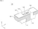
- FIG. 1is a perspective view illustrating a light emitting device package according to an exemplary embodiment of the present invention.
- FIG. 2is a cross-sectional view illustrating the light emitting device package shown in FIG. 1 .
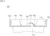
- FIG. 3is a cross-sectional view taken along a plane perpendicular to the plane of FIG. 2 , illustrating the light emitting device package shown in FIG. 1 .
- a longitudinal direction of the light emitting device packageis referred to as a "longitudinal direction Z”
- a horizontal direction perpendicular to the longitudinal direction Zis referred to as a “horizontal direction Y”
- a height direction perpendicular to both the longitudinal direction Z and the horizontal direction Yis referred to as a "height direction X”.
- FIG. 2is a cross-sectional view taken along an X-Y plane of the light emitting device package shown in FIG. 1 , and viewed in the longitudinal direction Z
- FIG. 3is a cross-sectional view taken along a Z-X plane of the light emitting device package shown in FIG. 1 , and viewed in the horizontal direction Y.
- the light emitting device packagewhich is designated by reference numeral "100" includes a body 110 having a cavity while being provided, at a bottom surface thereof, with a recess 115, first and second lead frames 140 and 150 mounted in the cavity of the body 110, and a light source 130 mounted in the cavity of the body 110 while being electrically connected with the light source 130, wherein each one of the first and second lead frames 140 and 150 has a heat sink 160 which is extended from a portion of the first or the second lead frames 140 and 150, and the heat sink extending from the first lead frame 140 is disposed in the recess 115.
- the body 110includes a second coupler 175 formed on at least a portion of the body 110.
- the heat sink 160includes a first coupler 170, to which the second coupler 175 is coupled.
- the body 110may be made of at least one selected from among a resin such as Polyphthalamide (PPA), silicon (Si), aluminum (Al), aluminum nitride (AIN), a liquid crystal polymer such as photosensitive glass (PSG), polyamide 9T (PA9T), Sindiotactic polystyrene (SPS), a metal, sapphire (Al 2 O 3 ), and beryllium oxide (BeO), or may be a printed circuit board (PCB).
- the body 110may be formed by an injection molding process, an etching process or the like, although the present disclosure is not limited thereto.
- the body 110may have an inclined surface at an inner surface thereof. In accordance with the inclination of the inclined surface, the reflection angle of light emitted from the light source 130 may be varied. Thus, the orientation angle of outwardly emitted light may be adjusted.
- the cavityWhen viewing the cavity formed in the body 110 from the top side, the cavity may have a circular, square, polygonal, elliptical shape or the like and may have rounded corners.
- the cavityis not limited to the above-described shapes.
- the light source 130is electrically connected to the first and second lead frames 140 and 150.
- the light source 130may be wire-bonded to the first and second lead frames 140 and 150 by a wire 135.
- the light source 130may be, for example, a colored light emitting diode to emit red, green, blue and white light, or an ultraviolet (UV) light emitting diode to emit ultraviolet light, although the present disclosure is not limited thereto.
- a colored light emitting diodeto emit red, green, blue and white light
- an ultraviolet (UV) light emitting diodeto emit ultraviolet light
- One or more light emitting diodesmay be mounted.
- the light emitting diodemay be of a horizontal type wherein all electric terminals are disposed on an upper surface thereof, or of a vertical type wherein electric terminals are distributed on upper and lower surfaces thereof.
- the light emitting diodemay be of a flip-chip type.
- a resin encapsulator(not shown) may fill the cavity, to cover the light source 130.
- the resin encapsulator(not shown) may be made of silicon, epoxy resin, or other resin materials.
- the resin encapsulatormay be formed by filling the cavity with an encapsulating material, and curing the filled material using ultraviolet light or heat.
- the resin encapsulatormay include a fluorescent substance.
- the kind of the fluorescent substancemay be selected in accordance with the wavelength of light emitted from the light source 130 in order to realize emission of white light.
- the fluorescent substancemay be a blue, bluish green, green, yellowish green, yellow, yellowish red, orange, or red light-emitting fluorescent substance in accordance with the wavelength of light emitted from the light source 130, although the present disclosure is not limited thereto.
- the fluorescent substancemay be excited by light emitted from the light source 130 at a first wavelength, to generate light of a second wavelength.
- the light source 130is a blue light emitting diode
- the fluorescent substanceis a yellow fluorescent substance
- the yellow fluorescent substanceis excited by blue light, thereby emitting yellow light.
- the light emitting device package 100may provide white light as the blue light generated from the blue light emitting diode and the yellow light generated in accordance with excitation by the blue light are mixed.
- the light source 130when the light source 130 is a green light emitting diode, a magenta fluorescent substance or a mixture of blue and red fluorescent substances may be used as the fluorescent substance. Also, when the light source 130 is a red light emitting diode, a cyan fluorescent substance or a mixture of blue and green fluorescent substances may be used as the fluorescent substance.
- the first and second lead frames 140 and 150may be made of at least one of titanium (Ti), copper (Cu), nickel (Ni), gold (Au), chromium (Cr), tantalum (Ta), platinum (Pt), tin (Sn), silver (Ag), phosphor (P), aluminum (Al), indium (In), palladium (Pd), cobalt (Co), silicon (Si), germanium (Ge), hafnium (Hf), ruthenium (Ru), and iron (Fe), or an alloy thereof.
- the first and second lead frames 140 and 150may have a single-layer structure or a multilayer structure, although the present disclosure is not limited thereto.
- the first and second lead frames 140 and 150are spaced apart from each other, to be electrically isolated from each other.
- the first lead frame 140directly contacts the light source 130 or in an embodiment not forming part of the claimed invention, it may be electrically connected to the light source 130 via a material having conductivity.
- One of the first and second lead frames 140 and 150may function as an anode terminal, and the other of the first and second lead frames 140 and 150 may function as a cathode terminal.
- the second lead frame 150may be electrically connected to the light source 130 by the wire 135, although the present disclosure is not limited thereto. Accordingly, as a power source is connected to the first and second lead frames 140 and 150, electricity may be applied to the light source 130.
- a plurality of lead frames(not shown) are mounted in the body 110, and each of the lead frames (not shown) is electrically connected to associated ones of a plurality of light sources.
- the first lead frame 140has a heat sink 160 extended externally from the body 110 in the longitudinal direction Z of the body 110.
- Each one of the first and second lead frames 140 and 150has a longitudinal extension to form the heat sink 160.
- the extensionis bent to connect side surfaces of the body 110.
- a separate member(not shown) may be coupled to the first and second lead frames 140 and 150 such that it connects at least one side surface of the body 110.
- a materialsuch as a resin material having thermal conductivity may be coated over the side surfaces of the body 110.
- the present disclosureis not limited to the above-described structures.
- the heat sink 160may be made of the same material as the first and second lead frames 140 and 150, although the present disclosure is not limited thereto. That is, the heat sink may be made of at least one of titanium (Ti), copper (Cu), nickel (Ni), gold (Au), chromium (Cr), tantalum (Ta), platinum (Pt), tin (Sn), silver (Ag), phosphor (P), aluminum (Al), indium (In), palladium (Pd), cobalt (Co), silicon (Si), germanium (Ge), hafnium (Hf), ruthenium (Ru), and iron (Fe), or an alloy thereof, although the present disclosure is not limited thereto.
- the heat sinkmay be made of at least one of titanium (Ti), copper (Cu), nickel (Ni), gold (Au), chromium (Cr), tantalum (Ta), platinum (Pt), tin (Sn), silver (Ag), phosphor (P), aluminum (Al), indium (In), pal
- the heat sink 160is illustrated as extending from the first lead frame 140, as shown in FIG. 3 , it is formed to extend from each one of the first and second lead frames 140 and 150.
- a plurality of lead frames(not shown) may be formed, and a plurality of heat sinks 160 may extend from selected ones of the lead frames, although the present disclosure is not limited thereto.
- the heat sink 160is formed at the first lead frame 140, on which the light source 130 is mounted. In accordance with this structure, it may be possible to more effectively transfer heat generated in the light source 130 to the heat sink 160. Accordingly, the heat dissipation function of the light emitting device package 100 may be further enhanced.
- the heat sink 160may be formed at the anode terminal. Since heat dissipation of the light emitting device package 100 is mainly carried out at the anode terminal, it may be possible to more effectively achieve an increase in the heat dissipation effects of the light emitting device package 100.
- the heat sink 160includes a bent portion to bring the heat sink 160 into connect with the side surfaces of the body 110, respectively.
- a bent portionmay have a rounded portion.
- the bent portionmay be formed at corner regions of the body 110, respectively.
- the heat sink 160is formed to extend from the first and second lead frames 140 and 150 while extending along side surfaces of wall portions 120 of the body 110, it may be possible to further increase the exposed areas and volumes of the first and second lead frames 140 and 150, and thus to enhance the heat sink functions and heat dissipation functions of the first and second lead frames 140 and 150. Accordingly, it may be possible to achieve an enhancement in the reliability of the light emitting device package 100.
- the heat sink 160 of the first lead frame 140is bent to extend along the bottom surface of the body 110.
- the body 110is provided, at the bottom surface thereof, with the recess 115 to receive the extension portion of the heat sink 160.
- the body 110is provided with the recess 115, and the heat sink 160 is partially received in the recess 115, it may be possible to more stably form the heat sink 160.
- the recess 115has a depth greater than the thickness of the heat sink 160, and a width greater than the width of the heat sink 160, in order to allow the heat sink 160 to be more easily received in the recess 115.
- the body 110includes the recess 115, and the heat sink 160 is disposed in the recess 115, it may be possible to more reliably fix the heat sink 160 to the body 110.
- the heat sink 160includes the first coupler 170, and the body 110 includes the second coupler 175.
- the first coupler 170is formed at an inner surface of the heat sink 160 connecting the body 110.
- the first coupler 170includes at least one protrusion.
- the second coupler 175is formed to be engagable with the first coupler 170.
- the second coupler 175includes at least one groove.
- the second coupler 175may have a structure different from the illustrated structure, for example, a hole structure, so long as it may be coupled with the first coupler 170.
- the present disclosureis not limited to the above-described structures.
- first coupler 170which includes protrusions
- second coupler 175, which includes grooves, in order to correspond to the first coupler 170is formed at the body 110
- the present disclosureis not limited thereto.
- reversed structuresmay be employed. That is, protrusions (not shown) may be formed on at least a portion of the body 110, and grooves (not shown) corresponding to the protrusions (not shown) may be formed in at least a portion of the heat sink 160.
- the heat sink 160is provided with the first coupler 170, and the body 110 is provided with the second coupler 175 corresponding to the first coupler 170, it may be possible to more reliably fix the heat sink 160 to the body 110.
- FIG. 4is a cross-sectional view illustrating a light emitting device package according to another embodiment.
- the heat sink 160includes roughness 180 formed on at least a portion of the heat sink 160.
- the roughness 180is formed on an outer surface of the heat sink 160, although the present disclosure is not limited thereto.
- the heat sink 160includes the roughness (not shown), it may be possible to increase the surface area of the heat sink 160, and thus to achieve an enhancement in the heat dissipation effects of the heat sink 160.
- FIG. 5is a cross-sectional view illustrating a light emitting device package according to another embodiment.
- a bonding layer 190may be disposed between at least one surface of the body 110 and the heat sink 160.
- the bonding layer 190may be formed by coating a material of the bonding layer 190 over one side surface of the body 110, disposing the heat sink 160 to contact the coated bonding layer (not shown), and then curing the coated bonding layer (not shown), although the present disclosure is not limited thereto.
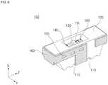
- FIG. 6is a perspective view illustrating a light emitting device package according to another embodiment.
- the heat sink 160may have holes 165.
- the holes 165may be formed by etching or pressing the heat sink 160, or preparing the first and second lead frames 140 and 150 to have the holes 165, although the present disclosure is not limited thereto. Although a plurality of holes 165 having a rectangular shape is formed at the heat sink 160, which is connected to the first lead frame 140, in the case of FIG. 6 , the holes 165 may be formed at the heat sink 160, which is connected to the second lead frame 150. Also, the holes 165 may have other shapes, for example, a circular shape or a polygonal shape, although the present disclosure is not limited thereto.
- a portion of the body 110may be protruded into at least one of the holes 165, or at least one of the holes 165 may be filled with a portion of the body 110, although the present disclosure is not limited thereto.
- the exposed area of the heat sink 160increases, thereby enhancing the heat sink function and heat dissipation effects of the heat sink 160.
- an enhancement in the reliability of the light emitting device package 100may be achieved.
- the light emitting device package according to any one of the above-described embodimentsmay be applied to a lighting system.
- the lighting systemmay be a lighting apparatus, in an embodiment of the claimed invention the lighting system is a backlight unit, examples not forming part of the claimed invention include a liquid crystal display device, etc, although the present disclosure is not limited thereto.
- FIG. 7Ais a perspective view illustrating a lighting apparatus including a light emitting device package according to an exemplary embodiment.
- FIG. 7Bis a cross-sectional view taken along a plane extending in a longitudinal direction Z and a height direction X and viewed in a horizontal direction Y, illustrating the lighting apparatus of FIG. 7A .
- the lighting apparatuswhich is designated by reference numeral "500” may include a body 510, a cover 530 coupled to the body 510, and end caps 550 located at both ends of the body 510.
- a light emitting device module 540is coupled to a lower surface of the body 510.
- the body 510may be made of a metal material exhibiting excellent conductivity and excellent heat radiation effects to outwardly dissipate heat generated from light emitting device packages 544 through an upper surface of the body 510.
- the light emitting device packages 544may be mounted on a printed circuit board (PCB) 542 in multiple rows while having various colors, to form a multi-color array.
- the light emitting device packages 544may be mounted at the same distance, or may be mounted at different distances to enable brightness adjustment, if necessary.
- the PCB 542may be a metal core PCB (MCPCB) or a PCB made of a flame retardant-4 (FR4) material.
- Each light emitting device package 544may include a heat sink (not shown) so that it may have an enhanced heat dissipation function. Thus, it may be possible to enhance the reliability and efficiency of the light emitting device package 544. In addition, it may be possible to extend the life span of the lighting apparatus 500, which includes the light emitting device packages 544.
- the cover 530may have a circular shape to surround the lower surface of the body 510, although the present disclosure is not limited thereto.
- the cover 530protects the light emitting device module 540 from external foreign matter, etc.
- the cover 530may contain light diffusion particles to achieve anti-glare effects and uniform emission of light generated from the light emitting device packages 544.
- At least one of the inner and outer surfaces of the cover 530may be provided with a prism pattern.
- a fluorescent substance layermay be coated over at least one of the inner and outer surfaces of the cover 530.
- the cover 530should have high light transmittance and heat resistance sufficient to endure heat generated from the light emitting device packages 544.
- the cover 530may be formed of polyethylene terephthalate (PET), polycarbonate (PC) or polymethylmethacrylate (PMMA).
- the end caps 550may be disposed at both ends of the body 510 and function to seal a power supply device (not shown). Each end cap 550 is provided with power pins 552, so that the lighting apparatus 500 in accordance with the illustrated embodiment may be directly connected to a terminal, which is provided for a conventional fluorescent lamp, without an additional connector.
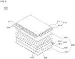
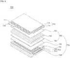
- FIG. 8is an exploded perspective view illustrating a liquid crystal display apparatus including a light emitting device according to an exemplary embodiment.
- FIG. 8illustrates an edge-light type liquid crystal display apparatus 600.
- the liquid crystal display apparatus 600may include a liquid crystal display panel 610 and a backlight unit 670 to supply light to the liquid crystal display panel 610.
- the liquid crystal display panel 610may display an image using the light supplied from the backlight unit 670.
- the liquid crystal display panel 610may include a color filter substrate 612 and a thin film transistor substrate 614, which are opposite each other with liquid crystals interposed therebetween.
- the color filter substrate 612may realize the color of an image displayed on the liquid crystal display panel 610.
- the thin film transistor substrate 614is electrically connected to a PCB 618, on which a plurality of circuit elements is mounted, by means of a drive film 617.
- the thin film transistor substrate 614may apply drive voltage provided by the PCB 618 to liquid crystals in response to a drive signal transmitted from the PCB 618.
- the thin film transistor substrate 614may include thin film transistors and pixel electrodes in the form of thin films formed on another substrate made of a transparent material such as glass or plastic.
- the backlight unit 670includes a light emitting device module 620 to emit light, a light guide plate 630 to change light emitted from the light emitting device module 620 into planar light and to transmit the planar light to the liquid crystal display panel 610, a plurality of films 650, 666 and 664 to achieve uniformity in brightness distribution and improved vertical incidence of light emerging from the light guide plate 630, and a reflection sheet 640 to reflect light emitted rearwards from the light guide plate 630 toward the light guide plate 630.
- the light emitting device module 620may include a plurality of light emitting device packages 624 and a PCB 622 on which the plurality of light emitting device packages 624 is mounted to form an array.
- each light emitting device package 624may include a heat sink (not shown) so that it may have an enhanced heat dissipation function.
- a heat sinknot shown
- the backlight unit 670may include a diffusion film 666 to diffuse light incident thereupon from the light guide plate 630 toward the liquid crystal display panel 610, and a prism film 650 to condense the diffused light so as to enhance vertical light incidence.
- the backlight unit 670may further include a protection film 664 to protect the prism film 650.
- FIG. 9is an exploded perspective view illustrating a liquid crystal display apparatus including a light emitting device according to another embodiment. The same configuration as that illustrated in FIG. 8 and described with reference to FIG. 8 will not be repeatedly described in detail.
- FIG. 9illustrates a direct type liquid crystal display apparatus 700 including a liquid crystal display panel 710 and a backlight unit 770 to supply light to the liquid crystal display panel 710.
- the liquid crystal display panel 710is identical to that of FIG. 8 and, as such, no detailed description thereof will be given.
- the backlight unit 770may include a plurality of light emitting device modules 723, a reflection sheet 724, a lower chassis 730 in which the light emitting device modules 723 and reflection sheet 724 are accommodated, and a diffusion sheet 740 and a plurality of optical films 760, which are disposed over the light emitting device modules 723.
- Each light emitting device module 723may include a plurality of light emitting device packages 722, and a PCB 721 on which the plurality of light emitting device packages 722 is mounted to form an array.
- each light emitting device package 722may include a heat sink (not shown) so that it may have an enhanced heat dissipation function.
- a heat sinknot shown
- the reflection sheet 724reflects light generated by the light emitting device packages 722 toward the liquid crystal display panel 710, to achieve an enhancement in light utilization efficiency.
- the optical films 760are disposed over the diffusion sheet 740.
- the optical films 760may include a diffusion film 766, a prism film 750 and a protection film 764.
- the heat sink formed to extend from the lead framesextend along a side surface of the body, so that it may be possible to enhance the heat sink function and heat dissipation function of the lead frames. Accordingly, it may be possible to obtain more excellent heat dissipation effects and to achieve an enhancement in reliability.
Landscapes
- Led Device Packages (AREA)
- Non-Portable Lighting Devices Or Systems Thereof (AREA)
Description
- This application claims the priority benefit of Korean Patent Application No.
10-2010-0118125 filed on November 25, 2010 - Embodiments relate to a light emitting device package.
- A light emitting diode (LED) is a device, which converts an electrical signal into light, using the characteristics of a compound semiconductor. Such an LED is applied to home electronic appliances, remote controllers, advertising display panels, indicators, various automation appliances, etc. The application range of LEDs is being gradually widened.
- Meanwhile, when electricity is applied to a light emitting device package, a considerable amount of heat is generated from the light emitting device package. This heat not only degrades the durability and reliability of the light emitting device package, but also limits the functions and lifespan of the light emitting device package.
US 2010 001308A1 discloses a side view light emitting diode package including a housing that includes a front side part and a rear side part integrally formed with the front side part, the front side part having a light emission part; and a lead frame that is located between the front side part and the rear side part.US 2006 043401 A1 discloses a high power LED package, in which a package body is integrally formed with resin to have a recess for receiving an LED chip.US 2006 133044 A1 discloses a leadframe that is configured to be used with an electronic device, e.g., light emitting diode (LED), including a heat sink supporting ring for supporting a heat sink, where an outer frame is spaced apart from the heat sink supporting ring, and encloses the heat sink supporting ring.JP 2008 108836 A JP 2006 318995 A WO 2008/002088 A1 .- Embodiments provide a light emitting device package including a lead frame having a lateral extension to increase an exposed portion of the lead frame, and thus to enhance the heat sink function and heat dissipation function of the lead frame, thereby being capable of exhibiting more excellent heat dissipation effects and achieving an enhancement in reliability. Embodiments of the invention are defined in the independent claim 1. Further preferred embodiments of the invention are defined in the dependent claims.
- In one embodiment, a light emitting device package includes a body comprising a cavity, and a recess formed at a bottom surface of the body, first and second lead frames mounted in the body, and a light source electrically connected with the first and second lead frames, wherein each of the first and second lead frames has a heat sink which is extended from a portion of the first or the second lead frames, and is disposed in the recess, wherein the body further comprises a second coupler formed on at least a portion of the body, and wherein the heat sink comprises a first coupler, to which the second coupler is coupled. The heat sink is contacted at least a portion of one side surface of the body.
- The heat sink has at least a portion contacting the recess.
- The heat sink may have at least one bent portion.
- The bent portion may be disposed at a corner region of the body.
- The bent portion may have a rounded portion.
- The heat sink is extended from the first lead frame. The light source is mounted on the first lead frame.
- The first lead frame may form an anode terminal.
- The recess has a width greater than a width of the heat sink.
- The recess has a depth greater than a thickness of the heat sink.
- In examples not forming part of the claimed invention, the first coupler may be a groove, and the second coupler may be a protrusion to be coupled with the groove.
- The first coupler is a protrusion, and the second coupler is a groove to be coupled with the protrusion.
- The heat sink may has a hole through at least a portion of the heat sink.
- At least a portion of the body may be protruded through the hole.
- The heat sink has at least a portion in which roughness are formed.
- The heat sink may be made of an identical material to the first and second lead frames.
- The light emitting device package may further include a bonding layer disposed between at least one side surface of the body and the heat sink.
- The heat sink may include a coating layer formed on at least a portion of a surface of the heat sink.
- Details of embodiments will be more clearly understood from the following detailed description taken in conjunction with the accompanying drawings, in which:
FIG. 1 is a perspective view illustrating a light emitting device package according to an exemplary embodiment of the present invention;FIG. 2 is a cross-sectional view illustrating the light emitting device package shown inFIG. 1 ;FIG. 3 is a cross-sectional view illustrating the light emitting device package shown inFIG. 1 ;FIG. 4 is a cross-sectional view illustrating a light emitting device package according to another embodiment;FIG. 5 is a cross-sectional view illustrating a light emitting device package according to another embodiment;FIG. 6 is a perspective view illustrating a light emitting device package according to another embodiment;FIG. 7A is a perspective view illustrating a lighting apparatus including a light emitting device package according to an exemplary embodiment;FIG. 7B is a cross-sectional view illustrating the lighting apparatus shown inFIG. 7A ;FIG. 8 is an exploded perspective view illustrating a liquid crystal display apparatus including a light emitting device according to an exemplary embodiment; andFIG. 9 is an exploded perspective view illustrating a liquid crystal display apparatus including a light emitting device according to another embodiment.- Reference will now be made in detail to embodiments, examples of which are illustrated in the accompanying drawings. In the drawings, the thickness or size of each layer is exaggerated, omitted, or schematically illustrated for convenience of description and clarity. Also, the size or area of each constituent element does not entirely reflect the actual size thereof. Wherever possible, the same reference numbers will be used throughout the drawings to refer to the same or like parts.
FIG. 1 is a perspective view illustrating a light emitting device package according to an exemplary embodiment of the present invention.FIG. 2 is a cross-sectional view illustrating the light emitting device package shown inFIG. 1 .FIG. 3 is a cross-sectional view taken along a plane perpendicular to the plane ofFIG. 2 , illustrating the light emitting device package shown inFIG. 1 .- In the following description, to explain the shape of the light emitting device package according to the illustrated embodiment in more detail, a longitudinal direction of the light emitting device package is referred to as a "longitudinal direction Z", a horizontal direction perpendicular to the longitudinal direction Z is referred to as a "horizontal direction Y", and a height direction perpendicular to both the longitudinal direction Z and the horizontal direction Y is referred to as a "height direction X".
- That is,
FIG. 2 is a cross-sectional view taken along an X-Y plane of the light emitting device package shown inFIG. 1 , and viewed in the longitudinal direction Z, andFIG. 3 is a cross-sectional view taken along a Z-X plane of the light emitting device package shown inFIG. 1 , and viewed in the horizontal direction Y. - Referring to
FIGS. 1 to 3 , the light emitting device package according to the illustrated embodiment, which is designated by reference numeral "100", includes abody 110 having a cavity while being provided, at a bottom surface thereof, with arecess 115, first and second lead frames 140 and 150 mounted in the cavity of thebody 110, and alight source 130 mounted in the cavity of thebody 110 while being electrically connected with thelight source 130, wherein each one of the first and second lead frames 140 and 150 has aheat sink 160 which is extended from a portion of the first or the second lead frames 140 and 150, and the heat sink extending from thefirst lead frame 140 is disposed in therecess 115. Thebody 110 includes asecond coupler 175 formed on at least a portion of thebody 110. Theheat sink 160 includes afirst coupler 170, to which thesecond coupler 175 is coupled. - The
body 110 may be made of at least one selected from among a resin such as Polyphthalamide (PPA), silicon (Si), aluminum (Al), aluminum nitride (AIN), a liquid crystal polymer such as photosensitive glass (PSG), polyamide 9T (PA9T), sindiotactic polystyrene (SPS), a metal, sapphire (Al2O3), and beryllium oxide (BeO), or may be a printed circuit board (PCB). Thebody 110 may be formed by an injection molding process, an etching process or the like, although the present disclosure is not limited thereto. - The
body 110 may have an inclined surface at an inner surface thereof. In accordance with the inclination of the inclined surface, the reflection angle of light emitted from thelight source 130 may be varied. Thus, the orientation angle of outwardly emitted light may be adjusted. - The smaller the orientation angle of light, the greater the convergence of light emitted from the
light source 130 to the outside. Conversely, the greater the orientation angle of light, the smaller the convergence of light emitted from thelight source 130 to the outside. - When viewing the cavity formed in the
body 110 from the top side, the cavity may have a circular, square, polygonal, elliptical shape or the like and may have rounded corners. Of course, the cavity is not limited to the above-described shapes. - The
light source 130 is electrically connected to the first and second lead frames 140 and 150. For example, thelight source 130 may be wire-bonded to the first and second lead frames 140 and 150 by awire 135. - The
light source 130 may be, for example, a colored light emitting diode to emit red, green, blue and white light, or an ultraviolet (UV) light emitting diode to emit ultraviolet light, although the present disclosure is not limited thereto. One or more light emitting diodes may be mounted. - The light emitting diode may be of a horizontal type wherein all electric terminals are disposed on an upper surface thereof, or of a vertical type wherein electric terminals are distributed on upper and lower surfaces thereof. Alternatively, the light emitting diode may be of a flip-chip type.
- A resin encapsulator (not shown) may fill the cavity, to cover the
light source 130. - The resin encapsulator (not shown) may be made of silicon, epoxy resin, or other resin materials. The resin encapsulator may be formed by filling the cavity with an encapsulating material, and curing the filled material using ultraviolet light or heat.
- The resin encapsulator (not shown) may include a fluorescent substance. The kind of the fluorescent substance may be selected in accordance with the wavelength of light emitted from the
light source 130 in order to realize emission of white light. - The fluorescent substance may be a blue, bluish green, green, yellowish green, yellow, yellowish red, orange, or red light-emitting fluorescent substance in accordance with the wavelength of light emitted from the
light source 130, although the present disclosure is not limited thereto. - That is, the fluorescent substance may be excited by light emitted from the
light source 130 at a first wavelength, to generate light of a second wavelength. For example, when thelight source 130 is a blue light emitting diode, and the fluorescent substance is a yellow fluorescent substance, the yellow fluorescent substance is excited by blue light, thereby emitting yellow light. In this case, the light emittingdevice package 100 may provide white light as the blue light generated from the blue light emitting diode and the yellow light generated in accordance with excitation by the blue light are mixed. - Similarly, when the
light source 130 is a green light emitting diode, a magenta fluorescent substance or a mixture of blue and red fluorescent substances may be used as the fluorescent substance. Also, when thelight source 130 is a red light emitting diode, a cyan fluorescent substance or a mixture of blue and green fluorescent substances may be used as the fluorescent substance. - The fluorescent substance may be a known fluorescent substance such as a YAG-based, TAG-based, sulfide-based, silicate-based, aluminate-based, nitride-based, carbide-based, nitridosilicate-based, borate-based, fluoride-based, or phosphate-based fluorescent substance.
- The first and second lead frames 140 and 150 may be made of at least one of titanium (Ti), copper (Cu), nickel (Ni), gold (Au), chromium (Cr), tantalum (Ta), platinum (Pt), tin (Sn), silver (Ag), phosphor (P), aluminum (Al), indium (In), palladium (Pd), cobalt (Co), silicon (Si), germanium (Ge), hafnium (Hf), ruthenium (Ru), and iron (Fe), or an alloy thereof. The first and second lead frames 140 and 150 may have a single-layer structure or a multilayer structure, although the present disclosure is not limited thereto.
- The first and second lead frames 140 and 150 are spaced apart from each other, to be electrically isolated from each other. The
first lead frame 140 directly contacts thelight source 130 or in an embodiment not forming part of the claimed invention, it may be electrically connected to thelight source 130 via a material having conductivity. One of the first and second lead frames 140 and 150 may function as an anode terminal, and the other of the first and second lead frames 140 and 150 may function as a cathode terminal. Also, thesecond lead frame 150 may be electrically connected to thelight source 130 by thewire 135, although the present disclosure is not limited thereto. Accordingly, as a power source is connected to the first and second lead frames 140 and 150, electricity may be applied to thelight source 130. Meanwhile, a plurality of lead frames (not shown) are mounted in thebody 110, and each of the lead frames (not shown) is electrically connected to associated ones of a plurality of light sources. - The
first lead frame 140 has aheat sink 160 extended externally from thebody 110 in the longitudinal direction Z of thebody 110. Each one of the first and second lead frames 140 and 150 has a longitudinal extension to form theheat sink 160. The extension is bent to connect side surfaces of thebody 110. Alternatively, in an example not forming part of the claimed invention, a separate member (not shown) may be coupled to the first and second lead frames 140 and 150 such that it connects at least one side surface of thebody 110. Alternatively, in an example not forming part of the claimed invention, a material such as a resin material having thermal conductivity may be coated over the side surfaces of thebody 110. Of course, the present disclosure is not limited to the above-described structures. - Meanwhile, the
heat sink 160 may be made of the same material as the first and second lead frames 140 and 150, although the present disclosure is not limited thereto. That is, the heat sink may be made of at least one of titanium (Ti), copper (Cu), nickel (Ni), gold (Au), chromium (Cr), tantalum (Ta), platinum (Pt), tin (Sn), silver (Ag), phosphor (P), aluminum (Al), indium (In), palladium (Pd), cobalt (Co), silicon (Si), germanium (Ge), hafnium (Hf), ruthenium (Ru), and iron (Fe), or an alloy thereof, although the present disclosure is not limited thereto. - Although the
heat sink 160 is illustrated as extending from thefirst lead frame 140, as shown inFIG. 3 , it is formed to extend from each one of the first and second lead frames 140 and 150. A plurality of lead frames (not shown) may be formed, and a plurality ofheat sinks 160 may extend from selected ones of the lead frames, although the present disclosure is not limited thereto. - Meanwhile, the
heat sink 160 is formed at thefirst lead frame 140, on which thelight source 130 is mounted. In accordance with this structure, it may be possible to more effectively transfer heat generated in thelight source 130 to theheat sink 160. Accordingly, the heat dissipation function of the light emittingdevice package 100 may be further enhanced. - The
heat sink 160 may be formed at the anode terminal. Since heat dissipation of the light emittingdevice package 100 is mainly carried out at the anode terminal, it may be possible to more effectively achieve an increase in the heat dissipation effects of the light emittingdevice package 100. - The
heat sink 160 includes a bent portion to bring theheat sink 160 into connect with the side surfaces of thebody 110, respectively. A bent portion may have a rounded portion. The bent portion may be formed at corner regions of thebody 110, respectively. - Since the
heat sink 160 is formed to extend from the first and second lead frames 140 and 150 while extending along side surfaces ofwall portions 120 of thebody 110, it may be possible to further increase the exposed areas and volumes of the first and second lead frames 140 and 150, and thus to enhance the heat sink functions and heat dissipation functions of the first and second lead frames 140 and 150. Accordingly, it may be possible to achieve an enhancement in the reliability of the light emittingdevice package 100. - Meanwhile, the
heat sink 160 of thefirst lead frame 140 is bent to extend along the bottom surface of thebody 110. As described above, thebody 110 is provided, at the bottom surface thereof, with therecess 115 to receive the extension portion of theheat sink 160. As thebody 110 is provided with therecess 115, and theheat sink 160 is partially received in therecess 115, it may be possible to more stably form theheat sink 160. - The
recess 115 has a depth greater than the thickness of theheat sink 160, and a width greater than the width of theheat sink 160, in order to allow theheat sink 160 to be more easily received in therecess 115. - As the
body 110 includes therecess 115, and theheat sink 160 is disposed in therecess 115, it may be possible to more reliably fix theheat sink 160 to thebody 110. - Meanwhile, referring to
FIG. 3 , theheat sink 160 includes thefirst coupler 170, and thebody 110 includes thesecond coupler 175. Thefirst coupler 170 is formed at an inner surface of theheat sink 160 connecting thebody 110. Thefirst coupler 170 includes at least one protrusion. Thesecond coupler 175 is formed to be engagable with thefirst coupler 170. Thesecond coupler 175 includes at least one groove. Meanwhile, in an example not forming part of the claimed invention, thesecond coupler 175 may have a structure different from the illustrated structure, for example, a hole structure, so long as it may be coupled with thefirst coupler 170. Of course, the present disclosure is not limited to the above-described structures. - Although the
first coupler 170, which includes protrusions, is formed at theheat sink 160, and thesecond coupler 175, which includes grooves, in order to correspond to thefirst coupler 170, is formed at thebody 110, in the case ofFIG. 3 , the present disclosure is not limited thereto. In examples not forming part of the claimed invention, reversed structures may be employed. That is, protrusions (not shown) may be formed on at least a portion of thebody 110, and grooves (not shown) corresponding to the protrusions (not shown) may be formed in at least a portion of theheat sink 160. - As the
heat sink 160 is provided with thefirst coupler 170, and thebody 110 is provided with thesecond coupler 175 corresponding to thefirst coupler 170, it may be possible to more reliably fix theheat sink 160 to thebody 110. FIG. 4 is a cross-sectional view illustrating a light emitting device package according to another embodiment.- Referring to
FIG. 4 , theheat sink 160 includesroughness 180 formed on at least a portion of theheat sink 160. Theroughness 180 is formed on an outer surface of theheat sink 160, although the present disclosure is not limited thereto. - As the
heat sink 160 includes the roughness (not shown), it may be possible to increase the surface area of theheat sink 160, and thus to achieve an enhancement in the heat dissipation effects of theheat sink 160. FIG. 5 is a cross-sectional view illustrating a light emitting device package according to another embodiment.- Referring to
FIG. 5 , abonding layer 190 may be disposed between at least one surface of thebody 110 and theheat sink 160. - As the
bonding layer 190 is disposed between thebody 110 and theheat sink 160, it may be possible to reliably fix theheat sink 160 to thebody 110. Thebonding layer 190 may be formed by coating a material of thebonding layer 190 over one side surface of thebody 110, disposing theheat sink 160 to contact the coated bonding layer (not shown), and then curing the coated bonding layer (not shown), although the present disclosure is not limited thereto. FIG. 6 is a perspective view illustrating a light emitting device package according to another embodiment.- Referring to
FIG. 6 , theheat sink 160 may haveholes 165. - The
holes 165 may be formed by etching or pressing theheat sink 160, or preparing the first and second lead frames 140 and 150 to have theholes 165, although the present disclosure is not limited thereto. Although a plurality ofholes 165 having a rectangular shape is formed at theheat sink 160, which is connected to thefirst lead frame 140, in the case ofFIG. 6 , theholes 165 may be formed at theheat sink 160, which is connected to thesecond lead frame 150. Also, theholes 165 may have other shapes, for example, a circular shape or a polygonal shape, although the present disclosure is not limited thereto. - Meanwhile, a portion of the
body 110 may be protruded into at least one of theholes 165, or at least one of theholes 165 may be filled with a portion of thebody 110, although the present disclosure is not limited thereto. - As the
holes 165 are formed at theheat sink 160, the exposed area of theheat sink 160 increases, thereby enhancing the heat sink function and heat dissipation effects of theheat sink 160. Thus, an enhancement in the reliability of the light emittingdevice package 100 may be achieved. - The light emitting device package according to any one of the above-described embodiments may be applied to a lighting system. The lighting system may be a lighting apparatus, in an embodiment of the claimed invention the lighting system is a backlight unit, examples not forming part of the claimed invention include a liquid crystal display device, etc, although the present disclosure is not limited thereto.
FIG. 7A is a perspective view illustrating a lighting apparatus including a light emitting device package according to an exemplary embodiment.FIG. 7B is a cross-sectional view taken along a plane extending in a longitudinal direction Z and a height direction X and viewed in a horizontal direction Y, illustrating the lighting apparatus ofFIG. 7A .- Referring to
FIGS. 7A and7B , the lighting apparatus, which is designated by reference numeral "500" may include abody 510, acover 530 coupled to thebody 510, and endcaps 550 located at both ends of thebody 510. - A light emitting
device module 540 is coupled to a lower surface of thebody 510. Thebody 510 may be made of a metal material exhibiting excellent conductivity and excellent heat radiation effects to outwardly dissipate heat generated from light emitting device packages 544 through an upper surface of thebody 510. - The light emitting device packages 544 may be mounted on a printed circuit board (PCB) 542 in multiple rows while having various colors, to form a multi-color array. The light emitting device packages 544 may be mounted at the same distance, or may be mounted at different distances to enable brightness adjustment, if necessary. The
PCB 542 may be a metal core PCB (MCPCB) or a PCB made of a flame retardant-4 (FR4) material. - Each light emitting
device package 544 may include a heat sink (not shown) so that it may have an enhanced heat dissipation function. Thus, it may be possible to enhance the reliability and efficiency of the light emittingdevice package 544. In addition, it may be possible to extend the life span of thelighting apparatus 500, which includes the light emitting device packages 544. - The
cover 530 may have a circular shape to surround the lower surface of thebody 510, although the present disclosure is not limited thereto. - The
cover 530 protects the light emittingdevice module 540 from external foreign matter, etc. Thecover 530 may contain light diffusion particles to achieve anti-glare effects and uniform emission of light generated from the light emitting device packages 544. At least one of the inner and outer surfaces of thecover 530 may be provided with a prism pattern. Also, a fluorescent substance layer may be coated over at least one of the inner and outer surfaces of thecover 530. - Since the light generated from the light emitting device packages 544 is outwardly emitted through the
cover 530, thecover 530 should have high light transmittance and heat resistance sufficient to endure heat generated from the light emitting device packages 544. To this end, thecover 530 may be formed of polyethylene terephthalate (PET), polycarbonate (PC) or polymethylmethacrylate (PMMA). - The end caps 550 may be disposed at both ends of the
body 510 and function to seal a power supply device (not shown). Eachend cap 550 is provided withpower pins 552, so that thelighting apparatus 500 in accordance with the illustrated embodiment may be directly connected to a terminal, which is provided for a conventional fluorescent lamp, without an additional connector. FIG. 8 is an exploded perspective view illustrating a liquid crystal display apparatus including a light emitting device according to an exemplary embodiment.FIG. 8 illustrates an edge-light type liquidcrystal display apparatus 600. The liquidcrystal display apparatus 600 may include a liquidcrystal display panel 610 and abacklight unit 670 to supply light to the liquidcrystal display panel 610.- The liquid
crystal display panel 610 may display an image using the light supplied from thebacklight unit 670. The liquidcrystal display panel 610 may include acolor filter substrate 612 and a thinfilm transistor substrate 614, which are opposite each other with liquid crystals interposed therebetween. - The
color filter substrate 612 may realize the color of an image displayed on the liquidcrystal display panel 610. - The thin
film transistor substrate 614 is electrically connected to aPCB 618, on which a plurality of circuit elements is mounted, by means of adrive film 617. The thinfilm transistor substrate 614 may apply drive voltage provided by thePCB 618 to liquid crystals in response to a drive signal transmitted from thePCB 618. - The thin
film transistor substrate 614 may include thin film transistors and pixel electrodes in the form of thin films formed on another substrate made of a transparent material such as glass or plastic. - The
backlight unit 670 includes a light emittingdevice module 620 to emit light, alight guide plate 630 to change light emitted from the light emittingdevice module 620 into planar light and to transmit the planar light to the liquidcrystal display panel 610, a plurality offilms light guide plate 630, and areflection sheet 640 to reflect light emitted rearwards from thelight guide plate 630 toward thelight guide plate 630. - The light emitting
device module 620 may include a plurality of light emitting device packages 624 and aPCB 622 on which the plurality of light emitting device packages 624 is mounted to form an array. - In particular, each light emitting
device package 624 may include a heat sink (not shown) so that it may have an enhanced heat dissipation function. Thus, it may be possible to enhance the reliability and efficiency of the light emittingdevice package 624. In addition, it may be possible to extend the life span of thelighting apparatus 600, which includes the light emitting device packages 624. - Meanwhile, the
backlight unit 670 may include adiffusion film 666 to diffuse light incident thereupon from thelight guide plate 630 toward the liquidcrystal display panel 610, and aprism film 650 to condense the diffused light so as to enhance vertical light incidence. Thebacklight unit 670 may further include aprotection film 664 to protect theprism film 650. FIG. 9 is an exploded perspective view illustrating a liquid crystal display apparatus including a light emitting device according to another embodiment. The same configuration as that illustrated inFIG. 8 and described with reference toFIG. 8 will not be repeatedly described in detail.FIG. 9 illustrates a direct type liquidcrystal display apparatus 700 including a liquidcrystal display panel 710 and abacklight unit 770 to supply light to the liquidcrystal display panel 710.- The liquid
crystal display panel 710 is identical to that ofFIG. 8 and, as such, no detailed description thereof will be given. - The
backlight unit 770 may include a plurality of light emittingdevice modules 723, areflection sheet 724, alower chassis 730 in which the light emittingdevice modules 723 andreflection sheet 724 are accommodated, and adiffusion sheet 740 and a plurality of optical films 760, which are disposed over the light emittingdevice modules 723. - Each light emitting
device module 723 may include a plurality of light emitting device packages 722, and aPCB 721 on which the plurality of light emitting device packages 722 is mounted to form an array. - In particular, each light emitting
device package 722 may include a heat sink (not shown) so that it may have an enhanced heat dissipation function. Thus, it may be possible to enhance the reliability and efficiency of the light emittingdevice package 722. In addition, it may be possible to extend the life span of thebacklight unit 770, which includes the light emitting device packages 722. - The
reflection sheet 724 reflects light generated by the light emitting device packages 722 toward the liquidcrystal display panel 710, to achieve an enhancement in light utilization efficiency. - Meanwhile, the light generated from the light emitting
device modules 723 is incident upon thediffusion sheet 740. The optical films 760 are disposed over thediffusion sheet 740. The optical films 760 may include adiffusion film 766, aprism film 750 and aprotection film 764. - As apparent from the above description, in the light emitting device package according to each of the above-described embodiments, the heat sink formed to extend from the lead frames extend along a side surface of the body, so that it may be possible to enhance the heat sink function and heat dissipation function of the lead frames. Accordingly, it may be possible to obtain more excellent heat dissipation effects and to achieve an enhancement in reliability.
- Although embodiments have been described with reference to a number of illustrative embodiments thereof, it should be understood that numerous other modifications and applications may be devised by those skilled in the art that will fall within the intrinsic aspects of the embodiments. More particularly, various variations and modifications are possible in concrete constituent elements of the embodiments. The embodiments of the invention are defined in the appended claims.
Claims (7)
- A light emitting device package (100) comprising:a body (110) comprising a cavity surrounded by wall portions (120) having side surfaces;first and second lead frames (140, 150) mounted in the body (110); anda light emitting diode (130) electrically connected with the first and second lead frames (140, 150) disposed in the cavity;wherein the light emitting diode (130) is disposed on the first lead frame (140) in the cavity,wherein the first and second lead frames (140, 150) have a heat sink (160) which is extended, respectively, from a portion of the first and the second lead frames (140, 150) in the longitudinal direction (Z) of the body (110) while extending along side surfaces of the wall portions (120) of the body (110), and wherein the body (110) further comprises a recess (115) formed at a bottom surface of the body (110), and a portion of the heat sink (160) of the first lead frame (140) is bent to extend along the bottom surface of the body (110) and is disposed in the recess (115), the bottom surface arranged at the opposite to the light emission surface of the light emitting device package (100) with respect to the body (110), andwherein the recess (115) has a width greater than a width of the heat sink (160), and the recess (115) has a depth greater than a thickness of the heat sink (160),wherein the heat sink (160) further comprises a first coupler and the body (110) further comprises a second coupler (175), to which the first coupler is coupled,wherein the first coupler is a protrusion (170) formed at an inner surface of the heat sink (160) which connects to the side surfaces of the wall portions (120) of the body (110); wherein the second coupler is a groove (175) formed in order to correspond to the first coupler, and wherein the heat sink (160) has at least a portion on an outer surface thereof on which roughness is formed such that an enhancement in the heat dissipation effect of the heat sink (160) is achieved.
- The light emitting device package (100) according to claim 1, wherein the heat sink (160) is connected to at least a portion of one side surface of the body (110).
- The light emitting device package (100) according to claim 1, wherein the heat sink (160) has at least a portion contacting the recess (115).
- The light emitting device package (100) according to any one of claims 1 to 3, wherein the heat sink (160) has at least one bent portion, and
wherein the bent portion is disposed at a corner region of the body (110). - The light emitting device package (100) according to any one of claims 1 to 4, wherein the heat sink (160) has holes (165) through at least a portion of the heat sink (160), and wherein at least a portion of the body (110) is protruded through the holes (165).
- The light emitting device package (100) according to any one of claims 1 to 5, further comprising:
a bonding layer disposed between at least one side surface of the body (110) and the heat sink (160). - A backlight unit comprising a light emitting device package (100) according to any one of claims 1 to 6.
Applications Claiming Priority (1)
| Application Number | Priority Date | Filing Date | Title |
|---|---|---|---|
| KR1020100118125AKR101766720B1 (en) | 2010-11-25 | 2010-11-25 | Light Emitting Device Package |
Publications (3)
| Publication Number | Publication Date |
|---|---|
| EP2458655A2 EP2458655A2 (en) | 2012-05-30 |
| EP2458655A3 EP2458655A3 (en) | 2014-06-11 |
| EP2458655B1true EP2458655B1 (en) | 2021-04-21 |
Family
ID=44992791
Family Applications (1)
| Application Number | Title | Priority Date | Filing Date |
|---|---|---|---|
| EP11190050.2AActiveEP2458655B1 (en) | 2010-11-25 | 2011-11-22 | Light emitting device package |
Country Status (4)
| Country | Link |
|---|---|
| US (1) | US20120074456A1 (en) |
| EP (1) | EP2458655B1 (en) |
| KR (1) | KR101766720B1 (en) |
| CN (1) | CN102479911B (en) |
Families Citing this family (4)
| Publication number | Priority date | Publication date | Assignee | Title |
|---|---|---|---|---|
| USD786840S1 (en)* | 2016-02-25 | 2017-05-16 | Airgrain Incorporated | Antenna |
| EP3544066A1 (en)* | 2018-03-23 | 2019-09-25 | Excellence Opto. Inc. | High heat dissipation light emitting diode package structure having at least two light cups and lateral light emission |
| KR20220036670A (en)* | 2020-09-16 | 2022-03-23 | 삼성전자주식회사 | Display appartus and manufacturing method of the same |
| JP2023082632A (en)* | 2021-12-02 | 2023-06-14 | スタンレー電気株式会社 | semiconductor light emitting device |
Citations (5)
| Publication number | Priority date | Publication date | Assignee | Title |
|---|---|---|---|---|
| US6848819B1 (en)* | 1999-05-12 | 2005-02-01 | Osram Opto Semiconductors Gmbh | Light-emitting diode arrangement |
| US20060097366A1 (en)* | 2003-07-19 | 2006-05-11 | Ns Electronics Bangkok (1993) Ltd. | Semiconductor package including leadframe roughened with chemical etchant to prevent separation between leadframe and molding compound |
| WO2008002088A1 (en)* | 2006-06-30 | 2008-01-03 | Seoul Semiconductor Co., Ltd. | Leadframe having a heat sink supporting part, fabricating method of the light emitting diode package using the same and light emitting diode package fabricated by the method |
| US20090267104A1 (en)* | 2008-04-28 | 2009-10-29 | Lighthouse Technology Co., Ltd | Light-emitting diode package |
| US20100127302A1 (en)* | 2008-11-27 | 2010-05-27 | Samsung Led Co., Ltd. | Light emitting diode package |
Family Cites Families (15)
| Publication number | Priority date | Publication date | Assignee | Title |
|---|---|---|---|---|
| KR100214463B1 (en)* | 1995-12-06 | 1999-08-02 | 구본준 | Lead frame of clip type and method manufacture of the package |
| CN1685578B (en)* | 2002-09-30 | 2010-12-08 | 三洋电机株式会社 | Light emitting element |
| JP2006049442A (en)* | 2004-08-02 | 2006-02-16 | Sharp Corp | Semiconductor light emitting device and manufacturing method thereof |
| KR100587020B1 (en)* | 2004-09-01 | 2006-06-08 | 삼성전기주식회사 | High power light emitting diode package |
| EP1825524A4 (en)* | 2004-12-16 | 2010-06-16 | Seoul Semiconductor Co Ltd | CONNECTION GRID COMPRISING A THERMAL DISSIPATOR SUPPORT RING, METHOD FOR MANUFACTURING LIGHT-EMITTING DIODE HOUSING USING THE SAME, AND LIGHT-EMITTING DIODE HOUSING MADE THEREBY |
| JP4945925B2 (en)* | 2005-05-10 | 2012-06-06 | 岩崎電気株式会社 | Multilayer light emitting diode device and reflective light emitting diode unit |
| JP4180092B2 (en)* | 2006-10-16 | 2008-11-12 | シャープ株式会社 | Optically coupled semiconductor device, optically coupled semiconductor device manufacturing method, and electronic apparatus |
| JP2008108836A (en)* | 2006-10-24 | 2008-05-08 | Sharp Corp | Semiconductor light emitting device and manufacturing method thereof |
| US7993038B2 (en)* | 2007-03-06 | 2011-08-09 | Toyoda Gosei Co., Ltd. | Light-emitting device |
| KR100801621B1 (en)* | 2007-06-05 | 2008-02-11 | 서울반도체 주식회사 | LED Package |
| WO2009130957A1 (en)* | 2008-04-23 | 2009-10-29 | シーアイ化成株式会社 | Package for light emitting diode, light emitting device, and light emitting device manufacturing method |
| KR100986202B1 (en)* | 2008-07-01 | 2010-10-07 | 알티전자 주식회사 | Side view light emitting diode package |
| US8368112B2 (en)* | 2009-01-14 | 2013-02-05 | Cree Huizhou Opto Limited | Aligned multiple emitter package |
| JP2010171073A (en)* | 2009-01-20 | 2010-08-05 | Showa Denko Kk | Light-emitting device, electrical device, and display |
| USD626095S1 (en)* | 2009-12-11 | 2010-10-26 | Everlight Electronics Co., Ltd. | Light emitting diode |
- 2010
- 2010-11-25KRKR1020100118125Apatent/KR101766720B1/ennot_activeExpired - Fee Related
- 2011
- 2011-11-22EPEP11190050.2Apatent/EP2458655B1/enactiveActive
- 2011-11-25CNCN201110382066.8Apatent/CN102479911B/enactiveActive
- 2011-11-25USUS13/304,510patent/US20120074456A1/ennot_activeAbandoned
Patent Citations (5)
| Publication number | Priority date | Publication date | Assignee | Title |
|---|---|---|---|---|
| US6848819B1 (en)* | 1999-05-12 | 2005-02-01 | Osram Opto Semiconductors Gmbh | Light-emitting diode arrangement |
| US20060097366A1 (en)* | 2003-07-19 | 2006-05-11 | Ns Electronics Bangkok (1993) Ltd. | Semiconductor package including leadframe roughened with chemical etchant to prevent separation between leadframe and molding compound |
| WO2008002088A1 (en)* | 2006-06-30 | 2008-01-03 | Seoul Semiconductor Co., Ltd. | Leadframe having a heat sink supporting part, fabricating method of the light emitting diode package using the same and light emitting diode package fabricated by the method |
| US20090267104A1 (en)* | 2008-04-28 | 2009-10-29 | Lighthouse Technology Co., Ltd | Light-emitting diode package |
| US20100127302A1 (en)* | 2008-11-27 | 2010-05-27 | Samsung Led Co., Ltd. | Light emitting diode package |
Also Published As
| Publication number | Publication date |
|---|---|
| US20120074456A1 (en) | 2012-03-29 |
| EP2458655A3 (en) | 2014-06-11 |
| KR101766720B1 (en) | 2017-08-23 |
| KR20120056543A (en) | 2012-06-04 |
| EP2458655A2 (en) | 2012-05-30 |
| CN102479911A (en) | 2012-05-30 |
| CN102479911B (en) | 2016-02-10 |
Similar Documents
| Publication | Publication Date | Title |
|---|---|---|
| US8613533B2 (en) | Optical sheet and light emitting device package having the same | |
| US20110175119A1 (en) | Light emitting apparatus and lighting system | |
| EP2458655B1 (en) | Light emitting device package | |
| KR20110105056A (en) | Light emitting device, light emitting device manufacturing method, light unit and lighting device | |
| KR101941512B1 (en) | Light emitting device | |
| KR101849126B1 (en) | Light Emitting Device Package | |
| KR101781043B1 (en) | Light-emitting element array | |
| KR101781047B1 (en) | Light emitting device package | |
| KR102042208B1 (en) | Printed Circuit Board | |
| KR101818752B1 (en) | Light emitting device array | |
| KR101883344B1 (en) | Light Emitting Device Array | |
| KR101722622B1 (en) | The light- | |
| KR101735310B1 (en) | Light Emitting Device Package | |
| KR20120073929A (en) | Light emitting device package | |
| KR20120072737A (en) | Light emitting device package | |
| KR101831278B1 (en) | Light-emitting device | |
| KR101843734B1 (en) | Light emitting device array | |
| KR101722627B1 (en) | Light Emitting Device Module | |
| KR101894933B1 (en) | Light Emitting Device Package | |
| KR101807097B1 (en) | Light emitting device module | |
| KR20140089804A (en) | Light-emitting device | |
| KR20120034484A (en) | Light emitting device package | |
| KR20120035464A (en) | Light emitting device package | |
| KR20120045540A (en) | Light emitting device package | |
| KR20130048541A (en) | Light emitting diode module |
Legal Events
| Date | Code | Title | Description |
|---|---|---|---|
| PUAI | Public reference made under article 153(3) epc to a published international application that has entered the european phase | Free format text:ORIGINAL CODE: 0009012 | |
| AK | Designated contracting states | Kind code of ref document:A2 Designated state(s):AL AT BE BG CH CY CZ DE DK EE ES FI FR GB GR HR HU IE IS IT LI LT LU LV MC MK MT NL NO PL PT RO RS SE SI SK SM TR | |
| AX | Request for extension of the european patent | Extension state:BA ME | |
| PUAL | Search report despatched | Free format text:ORIGINAL CODE: 0009013 | |
| AK | Designated contracting states | Kind code of ref document:A3 Designated state(s):AL AT BE BG CH CY CZ DE DK EE ES FI FR GB GR HR HU IE IS IT LI LT LU LV MC MK MT NL NO PL PT RO RS SE SI SK SM TR | |
| AX | Request for extension of the european patent | Extension state:BA ME | |
| RIC1 | Information provided on ipc code assigned before grant | Ipc:H01L 33/62 20100101ALI20140506BHEP Ipc:H01L 33/48 20100101AFI20140506BHEP Ipc:H01L 33/64 20100101ALI20140506BHEP | |
| 17P | Request for examination filed | Effective date:20141021 | |
| RBV | Designated contracting states (corrected) | Designated state(s):AL AT BE BG CH CY CZ DE DK EE ES FI FR GB GR HR HU IE IS IT LI LT LU LV MC MK MT NL NO PL PT RO RS SE SI SK SM TR | |
| STAA | Information on the status of an ep patent application or granted ep patent | Free format text:STATUS: EXAMINATION IS IN PROGRESS | |
| RAP1 | Party data changed (applicant data changed or rights of an application transferred) | Owner name:LG INNOTEK CO., LTD. | |
| 17Q | First examination report despatched | Effective date:20170426 | |
| GRAP | Despatch of communication of intention to grant a patent | Free format text:ORIGINAL CODE: EPIDOSNIGR1 | |
| STAA | Information on the status of an ep patent application or granted ep patent | Free format text:STATUS: GRANT OF PATENT IS INTENDED | |
| INTG | Intention to grant announced | Effective date:20210205 | |
| GRAS | Grant fee paid | Free format text:ORIGINAL CODE: EPIDOSNIGR3 | |
| GRAA | (expected) grant | Free format text:ORIGINAL CODE: 0009210 | |
| STAA | Information on the status of an ep patent application or granted ep patent | Free format text:STATUS: THE PATENT HAS BEEN GRANTED | |
| AK | Designated contracting states | Kind code of ref document:B1 Designated state(s):AL AT BE BG CH CY CZ DE DK EE ES FI FR GB GR HR HU IE IS IT LI LT LU LV MC MK MT NL NO PL PT RO RS SE SI SK SM TR | |
| REG | Reference to a national code | Ref country code:GB Ref legal event code:FG4D | |
| REG | Reference to a national code | Ref country code:CH Ref legal event code:EP | |
| REG | Reference to a national code | Ref country code:DE Ref legal event code:R096 Ref document number:602011070738 Country of ref document:DE Ref country code:IE Ref legal event code:FG4D | |
| REG | Reference to a national code | Ref country code:AT Ref legal event code:REF Ref document number:1385560 Country of ref document:AT Kind code of ref document:T Effective date:20210515 | |
| REG | Reference to a national code | Ref country code:LT Ref legal event code:MG9D | |
| RAP2 | Party data changed (patent owner data changed or rights of a patent transferred) | Owner name:SUZHOU LEKIN SEMICONDUCTOR CO., LTD. | |
| REG | Reference to a national code | Ref country code:AT Ref legal event code:MK05 Ref document number:1385560 Country of ref document:AT Kind code of ref document:T Effective date:20210421 | |
| REG | Reference to a national code | Ref country code:DE Ref legal event code:R081 Ref document number:602011070738 Country of ref document:DE Owner name:SUZHOU LEKIN SEMICONDUCTOR CO. LTD., TAICANG, CN Free format text:FORMER OWNER: LG INNOTEK CO., LTD., SEOUL, KR | |
| REG | Reference to a national code | Ref country code:NL Ref legal event code:MP Effective date:20210421 | |
| PG25 | Lapsed in a contracting state [announced via postgrant information from national office to epo] | Ref country code:LT Free format text:LAPSE BECAUSE OF FAILURE TO SUBMIT A TRANSLATION OF THE DESCRIPTION OR TO PAY THE FEE WITHIN THE PRESCRIBED TIME-LIMIT Effective date:20210421 Ref country code:NL Free format text:LAPSE BECAUSE OF FAILURE TO SUBMIT A TRANSLATION OF THE DESCRIPTION OR TO PAY THE FEE WITHIN THE PRESCRIBED TIME-LIMIT Effective date:20210421 Ref country code:FI Free format text:LAPSE BECAUSE OF FAILURE TO SUBMIT A TRANSLATION OF THE DESCRIPTION OR TO PAY THE FEE WITHIN THE PRESCRIBED TIME-LIMIT Effective date:20210421 Ref country code:HR Free format text:LAPSE BECAUSE OF FAILURE TO SUBMIT A TRANSLATION OF THE DESCRIPTION OR TO PAY THE FEE WITHIN THE PRESCRIBED TIME-LIMIT Effective date:20210421 Ref country code:BG Free format text:LAPSE BECAUSE OF FAILURE TO SUBMIT A TRANSLATION OF THE DESCRIPTION OR TO PAY THE FEE WITHIN THE PRESCRIBED TIME-LIMIT Effective date:20210721 Ref country code:AT Free format text:LAPSE BECAUSE OF FAILURE TO SUBMIT A TRANSLATION OF THE DESCRIPTION OR TO PAY THE FEE WITHIN THE PRESCRIBED TIME-LIMIT Effective date:20210421 | |
| PG25 | Lapsed in a contracting state [announced via postgrant information from national office to epo] | Ref country code:SE Free format text:LAPSE BECAUSE OF FAILURE TO SUBMIT A TRANSLATION OF THE DESCRIPTION OR TO PAY THE FEE WITHIN THE PRESCRIBED TIME-LIMIT Effective date:20210421 Ref country code:RS Free format text:LAPSE BECAUSE OF FAILURE TO SUBMIT A TRANSLATION OF THE DESCRIPTION OR TO PAY THE FEE WITHIN THE PRESCRIBED TIME-LIMIT Effective date:20210421 Ref country code:LV Free format text:LAPSE BECAUSE OF FAILURE TO SUBMIT A TRANSLATION OF THE DESCRIPTION OR TO PAY THE FEE WITHIN THE PRESCRIBED TIME-LIMIT Effective date:20210421 Ref country code:GR Free format text:LAPSE BECAUSE OF FAILURE TO SUBMIT A TRANSLATION OF THE DESCRIPTION OR TO PAY THE FEE WITHIN THE PRESCRIBED TIME-LIMIT Effective date:20210722 Ref country code:IS Free format text:LAPSE BECAUSE OF FAILURE TO SUBMIT A TRANSLATION OF THE DESCRIPTION OR TO PAY THE FEE WITHIN THE PRESCRIBED TIME-LIMIT Effective date:20210821 Ref country code:PT Free format text:LAPSE BECAUSE OF FAILURE TO SUBMIT A TRANSLATION OF THE DESCRIPTION OR TO PAY THE FEE WITHIN THE PRESCRIBED TIME-LIMIT Effective date:20210823 Ref country code:NO Free format text:LAPSE BECAUSE OF FAILURE TO SUBMIT A TRANSLATION OF THE DESCRIPTION OR TO PAY THE FEE WITHIN THE PRESCRIBED TIME-LIMIT Effective date:20210721 Ref country code:PL Free format text:LAPSE BECAUSE OF FAILURE TO SUBMIT A TRANSLATION OF THE DESCRIPTION OR TO PAY THE FEE WITHIN THE PRESCRIBED TIME-LIMIT Effective date:20210421 Ref country code:ES Free format text:LAPSE BECAUSE OF FAILURE TO SUBMIT A TRANSLATION OF THE DESCRIPTION OR TO PAY THE FEE WITHIN THE PRESCRIBED TIME-LIMIT Effective date:20210421 | |
| REG | Reference to a national code | Ref country code:DE Ref legal event code:R097 Ref document number:602011070738 Country of ref document:DE | |
| PG25 | Lapsed in a contracting state [announced via postgrant information from national office to epo] | Ref country code:SK Free format text:LAPSE BECAUSE OF FAILURE TO SUBMIT A TRANSLATION OF THE DESCRIPTION OR TO PAY THE FEE WITHIN THE PRESCRIBED TIME-LIMIT Effective date:20210421 Ref country code:SM Free format text:LAPSE BECAUSE OF FAILURE TO SUBMIT A TRANSLATION OF THE DESCRIPTION OR TO PAY THE FEE WITHIN THE PRESCRIBED TIME-LIMIT Effective date:20210421 Ref country code:EE Free format text:LAPSE BECAUSE OF FAILURE TO SUBMIT A TRANSLATION OF THE DESCRIPTION OR TO PAY THE FEE WITHIN THE PRESCRIBED TIME-LIMIT Effective date:20210421 Ref country code:CZ Free format text:LAPSE BECAUSE OF FAILURE TO SUBMIT A TRANSLATION OF THE DESCRIPTION OR TO PAY THE FEE WITHIN THE PRESCRIBED TIME-LIMIT Effective date:20210421 Ref country code:DK Free format text:LAPSE BECAUSE OF FAILURE TO SUBMIT A TRANSLATION OF THE DESCRIPTION OR TO PAY THE FEE WITHIN THE PRESCRIBED TIME-LIMIT Effective date:20210421 Ref country code:RO Free format text:LAPSE BECAUSE OF FAILURE TO SUBMIT A TRANSLATION OF THE DESCRIPTION OR TO PAY THE FEE WITHIN THE PRESCRIBED TIME-LIMIT Effective date:20210421 | |
| PLBE | No opposition filed within time limit | Free format text:ORIGINAL CODE: 0009261 | |
| STAA | Information on the status of an ep patent application or granted ep patent | Free format text:STATUS: NO OPPOSITION FILED WITHIN TIME LIMIT | |
| 26N | No opposition filed | Effective date:20220124 | |
| PG25 | Lapsed in a contracting state [announced via postgrant information from national office to epo] | Ref country code:IS Free format text:LAPSE BECAUSE OF FAILURE TO SUBMIT A TRANSLATION OF THE DESCRIPTION OR TO PAY THE FEE WITHIN THE PRESCRIBED TIME-LIMIT Effective date:20210821 Ref country code:AL Free format text:LAPSE BECAUSE OF FAILURE TO SUBMIT A TRANSLATION OF THE DESCRIPTION OR TO PAY THE FEE WITHIN THE PRESCRIBED TIME-LIMIT Effective date:20210421 | |
| PG25 | Lapsed in a contracting state [announced via postgrant information from national office to epo] | Ref country code:MC Free format text:LAPSE BECAUSE OF FAILURE TO SUBMIT A TRANSLATION OF THE DESCRIPTION OR TO PAY THE FEE WITHIN THE PRESCRIBED TIME-LIMIT Effective date:20210421 | |
| REG | Reference to a national code | Ref country code:CH Ref legal event code:PL | |
| GBPC | Gb: european patent ceased through non-payment of renewal fee | Effective date:20211122 | |
| PG25 | Lapsed in a contracting state [announced via postgrant information from national office to epo] | Ref country code:LU Free format text:LAPSE BECAUSE OF NON-PAYMENT OF DUE FEES Effective date:20211122 Ref country code:IT Free format text:LAPSE BECAUSE OF FAILURE TO SUBMIT A TRANSLATION OF THE DESCRIPTION OR TO PAY THE FEE WITHIN THE PRESCRIBED TIME-LIMIT Effective date:20210421 Ref country code:BE Free format text:LAPSE BECAUSE OF NON-PAYMENT OF DUE FEES Effective date:20211130 | |
| REG | Reference to a national code | Ref country code:BE Ref legal event code:MM Effective date:20211130 | |
| PG25 | Lapsed in a contracting state [announced via postgrant information from national office to epo] | Ref country code:IE Free format text:LAPSE BECAUSE OF NON-PAYMENT OF DUE FEES Effective date:20211122 Ref country code:GB Free format text:LAPSE BECAUSE OF NON-PAYMENT OF DUE FEES Effective date:20211122 | |
| PG25 | Lapsed in a contracting state [announced via postgrant information from national office to epo] | Ref country code:FR Free format text:LAPSE BECAUSE OF NON-PAYMENT OF DUE FEES Effective date:20211130 | |
| PG25 | Lapsed in a contracting state [announced via postgrant information from national office to epo] | Ref country code:HU Free format text:LAPSE BECAUSE OF FAILURE TO SUBMIT A TRANSLATION OF THE DESCRIPTION OR TO PAY THE FEE WITHIN THE PRESCRIBED TIME-LIMIT; INVALID AB INITIO Effective date:20111122 Ref country code:CY Free format text:LAPSE BECAUSE OF FAILURE TO SUBMIT A TRANSLATION OF THE DESCRIPTION OR TO PAY THE FEE WITHIN THE PRESCRIBED TIME-LIMIT Effective date:20210421 | |
| PG25 | Lapsed in a contracting state [announced via postgrant information from national office to epo] | Ref country code:LI Free format text:LAPSE BECAUSE OF NON-PAYMENT OF DUE FEES Effective date:20220630 Ref country code:CH Free format text:LAPSE BECAUSE OF NON-PAYMENT OF DUE FEES Effective date:20220630 | |
| PGFP | Annual fee paid to national office [announced via postgrant information from national office to epo] | Ref country code:DE Payment date:20231003 Year of fee payment:13 | |
| PG25 | Lapsed in a contracting state [announced via postgrant information from national office to epo] | Ref country code:MK Free format text:LAPSE BECAUSE OF FAILURE TO SUBMIT A TRANSLATION OF THE DESCRIPTION OR TO PAY THE FEE WITHIN THE PRESCRIBED TIME-LIMIT Effective date:20210421 | |
| PG25 | Lapsed in a contracting state [announced via postgrant information from national office to epo] | Ref country code:MT Free format text:LAPSE BECAUSE OF FAILURE TO SUBMIT A TRANSLATION OF THE DESCRIPTION OR TO PAY THE FEE WITHIN THE PRESCRIBED TIME-LIMIT Effective date:20210421 | |
| REG | Reference to a national code | Ref country code:DE Ref legal event code:R079 Ref document number:602011070738 Country of ref document:DE Free format text:PREVIOUS MAIN CLASS: H01L0033480000 Ipc:H10H0020850000 | |
| REG | Reference to a national code | Ref country code:DE Ref legal event code:R119 Ref document number:602011070738 Country of ref document:DE |