EP2453284B1 - Microscope - Google Patents
MicroscopeDownload PDFInfo
- Publication number
- EP2453284B1 EP2453284B1EP10797025.3AEP10797025AEP2453284B1EP 2453284 B1EP2453284 B1EP 2453284B1EP 10797025 AEP10797025 AEP 10797025AEP 2453284 B1EP2453284 B1EP 2453284B1
- Authority
- EP
- European Patent Office
- Prior art keywords
- light
- microscope apparatus
- illumination
- light shielding
- sample
- Prior art date
- Legal status (The legal status is an assumption and is not a legal conclusion. Google has not performed a legal analysis and makes no representation as to the accuracy of the status listed.)
- Active
Links
Images


Classifications
- G—PHYSICS
- G02—OPTICS
- G02B—OPTICAL ELEMENTS, SYSTEMS OR APPARATUS
- G02B21/00—Microscopes
- G02B21/06—Means for illuminating specimens
- G02B21/08—Condensers
- G02B21/086—Condensers for transillumination only
- G—PHYSICS
- G02—OPTICS
- G02B—OPTICAL ELEMENTS, SYSTEMS OR APPARATUS
- G02B21/00—Microscopes
- G02B21/18—Arrangements with more than one light path, e.g. for comparing two specimens
- G02B21/20—Binocular arrangements
- G02B21/22—Stereoscopic arrangements
Definitions
- the present inventionrelates to a microscope apparatus.
- a light source imageis formed near the pupil conjugate position of the objective lens by using a light source, such as a halogen lamp and the like, a collector lens, a deflection mirror, and a projection lens (see, for example, Patent Literature 1). Further, it is proposed that a light shielding element is arranged near the pupil conjugate position of the objective lens to enable switching between bright-field illumination and dark-field illumination.
- Patent Literature 1Japanese Patent Laid-Open No. 11-133308
- US 2007/0097498relates to a device for varying and adjusting transmitted illumination for microscopes, in which an illumination unit can be selectively coupled to different modules for darkfield illumination, brightfield illumination, and/or diffuse illumination and/or for adapting the object field.
- Document DE 10 2004 017 694 B3discloses an illumination apparatus for a stereo microscope.
- An object of the present inventionis to provide a microscope apparatus having an illumination apparatus in which, regardless of the observation magnification of the imaging optical system, the entrance pupil of the imaging optical system can be filled with illumination light, and the pupil conjugate image can be suitably restricted by the light shielding element.
- the illumination apparatusincludes a condenser lens which condenses the light emitted from the surface light emitter and irradiates the sample with the condensed light.
- the condenser lensincludes at least one surface formed in an aspheric shape.
- the condenser lensis configured by a lens array in which a plurality of lenses arranged in an array form.
- the surface light emitteris configured by including a light source, and a light guide plate having a light emitting surface and allowing light emitted from the light source to be emitted from the light emitting surface.
- the light sourceis configured by a plurality of white LEDs.
- the light sourceis configured by a plurality of LEDs, each having a different peak wavelength.
- At least one of the surface light emitter and the condenser lensis configured to be movable along the optical axis.
- the microscope apparatusWhen the microscope apparatus according to the present invention is configured as described above, it is possible that, regardless of the observation magnification of the imaging optical system, the entrance pupil of the imaging optical system is filled with the illumination light from the illumination apparatus, and that the oblique illumination is performed while the pupil conjugate image is suitably restricted by the light shielding element.
- Figure 1 and Figure 2show a single-objective binocular stereoscopic microscope apparatus (hereinafter referred to as "microscope apparatus 1") which is an example of the stereoscopic microscope apparatus.
- the optical system of the microscope apparatus 1includes an imaging optical system 3 which forms a primary image of a sample (sample surface S) by condensing light illuminated by an illumination apparatus 2 and transmitted through the sample (sample surface S), and eyepieces 4 each of which enables the primary image formed by the imaging optical system 3 to be magnified and observed.
- the imaging optical system 3is configured by including an objective lens 31 which condenses a luminous flux transmitted through the sample surface S and converts the luminous flux into a parallel luminous flux, variable power lens groups 32 each of which condenses the parallel luminous flux emitted from the objective lens 31 and changes the observation magnification (changes the magnification) of the image of the sample, and imaging lenses 33 each of which forms the primary image of the sample.
- the microscope apparatus 1includes: a base unit 101 in which the illumination apparatus 2 is incorporated; a variable power lens barrel 103 to which the objective lens 31 and the eyepieces 4 are attached and in which the variable power lens groups 32 and the imaging lenses 33 are incorporated; and a focusing apparatus 105. Further, a sample platform 102 with a transparent member embedded therein is provided on the upper surface of the base unit 101, and the illumination apparatus 2 irradiates a sample placed on the sample platform 102 with illumination light from below the sample. Note that the objective lens 31 is attached to an objective lens attachment unit 106 provided at a lower portion of the variable power lens barrel 103.
- the objective lens attachment unit 106is configured such that one objective lens can be selected from a plurality of predetermined low power objective lenses and a plurality of predetermined high power objective lenses, so as to be attached to the objective lens attachment unit 106, and where the objective lens attachment unit 106 is configured such that a plurality of objective lenses can be selected from a plurality of predetermined low power objective lenses and a plurality of predetermined high power objective lenses, so as to be attached to the objective lens attachment unit 106.
- each of the eyepieces 4is housed in an eyepiece barrel 104, and is attached to an upper portion of the variable power lens barrel 103.
- variable power lens group 32 and the imaging lens 33 for each of the left and right eyesare arranged.
- a variable power knob 107is arranged at the outer side of the variable power lens barrel 103.
- a movable group for changing the magnificationis included in the variable power lens group 32, and is moved in the optical axis direction by a predetermined movement amount corresponding to the rotation of the variable power knob 107.
- an adjustable diaphragmaperture stop
- the focusing apparatus 105includes a focusing knob 108, and a mechanism unit (not shown) which moves the variable power lens barrel 103 vertically along the axis of the variable power lens barrel 103 according to the rotation of the focusing knob 108.
- the illumination apparatus 2 incorporated in the base unit 101is configured by arranging in order: a light guide plate 21, as a surface light emitter, which uses, as a light source, a plurality of white LEDs or a plurality of LEDs each having a peak at a different wavelength, and which has a light emitting surface 21a as a planar light emitting region; a light shielding plate 22, as a light shielding element, which shields a part of a luminous flux emitted from the light emitting surface of the light guide plate 21; and a light diffusing element 23 having a diffusion surface which diffuses the luminous flux transmitted without being shielded by the light shielding plate 22.
- the light guide plate 21performs surface light emission by using various light sources, such as a point light source, such as an LED and the like, or a line light source, such as a cold cathode tube and the like.
- the light guide plate 21is configured such that a light source is arranged at an end surface of an acrylic plate having a certain structure, so as to make the light from the light source incident on the end surface, and such that the incident light is repeatedly reflected in the acrylic plate so that the uniform light with the total reflection angle or less is emitted from the surface (light emitting surface 21a) of the light guide plate 21.
- the light guide plate 21 having such structurecan be made very thin, and can perform uniform and very bright surface light emission.
- the thickness of the illumination apparatusis reduced to the thickness or less of the deflection mirror.
- the light guide plate 21is used as a surface light emitter, and thereby the thickness of the illumination apparatus 2 can be reduced.
- Figure 4(a)shows a relationship between a pupil conjugate image PI seen from the side of the sample surface S and the rectangular light shielding plate 22 in the case where the pupil conjugate image PI is restricted by inserting the light shielding plate 22 from one side into the optical path along the axis A shown in Figure 1 and Figure 3 .
- the normal vector of the light shielding plate 22is in parallel with the optical axis, and hence it is possible to obliquely illuminate the sample surface S by moving the light shielding plate 22 in the plane substantially vertical to the optical axis.
- the shape of the light shielding plate 22is not limited to the rectangular shape.
- a light shielding plate 22'which has a circular aperture 22a with a radius smaller than the effective diameter of the pupil conjugate image PI, may be inserted into the optical path.
- a light shielding plate 22" having a slit aperture 22bmay be inserted into the optical path.
- the aperture shape of the light shielding plate 22is not limited to the above-described aperture shapes, and a case is also included where oblique illumination is performed in such a manner that the light shielding plate 22, which is provided with an aperture having a shape other than the above-described aperture shapes and having an area smaller than the area of the pupil conjugate image PI, is moved in the plane substantially perpendicular to the optical axis.
- the principle that a phase object can be observed under oblique illuminationis already described in many literatures, and the like, and hence the detailed description thereof is omitted here.
- Figure 5is a graph in the case where the insertion direction (axis A) of the rectangular light shielding plate 22 shown in Figure 4(a) is taken as the abscissa, and where the light shielding rate of the light shielding plate 22 is taken as the ordinate.
- Figure 5(a)shows the case where the light shielding rate is set to about 100% over the entire surface
- Figure 5(b)shows the case where the light shielding rate on the insertion direction leading edge side is set to 50% and where the light shielding rate on the opposite side is set to 100%
- Figure 5(c)shows the case where the light shielding rate is continuously increased from the insertion direction leading edge side to the opposite side.
- the light shielding plate 22configured to have the transmittance distribution as shown in Figure 5(b) and Figure 5(c) can suppress glare due to excessive contrast to a greater extent than the light shielding plate 22 configured as shown in Figure 5 (a) , and hence is useful for the observation.
- the light shielding plate 22' provided with the circular aperture 22a as shown in Figure 4(b) and the light shielding plate 22" provided with the slit aperture 22b as shown in Figure 4(c)the light shielding plate, having the configuration in which, at the boundary portion between the aperture section and the light shielding section, the light shielding rate is continuously increased to eventually become 100%, is more useful for the observation of a sample with a large phase difference than the light shielding plate having the configuration in which the difference in the light shielding rate is 100% at the boundary portion between the aperture section and the light shielding section.
- the imaging optical system 3 in the microscope apparatus 1includes a plurality of kinds of objective lenses, and a variable power mechanism.
- the position of the conjugate image PI of the entrance pupil of the imaging optical system 3, which conjugate image PI is formed on the illumination side with the sample surface S as a boundaryis greatly changed according to the magnification of the variable power lens group 32.
- the variable power lens group 32is configured by including a fixed group 32a, a movable group 32b, and an aperture stop 32c.
- the conjugate image PI of the entrance pupil of the imaging optical system 3is formed at a place separated most from the sample surface S, or the real image is replaced by the virtual image so that the conjugate image PI of the entrance pupil is not formed on the illumination side.
- the illumination apparatus 2 incorporated in the base unit 101 of the microscope apparatus 1is configured, as shown in Figure 3 , such that the light diffusing element 23, which diffuses the luminous flux transmitted without being shielded by the light shielding plate 22, is arranged between the sample surface S and the light shielding plate 22.
- reference character Ddenotes an optical-axis direction interval between the light shielding plate 22 and the light diffusing element 23.
- the conjugate image of the entrance pupilis not only formed on the one plane (the plane of the conjugate image PI of the entrance pupil which plane is formed when the light diffusing element 23 is not arranged) having the optical axis as a normal, but also formed, by the diffused light, on each of a plurality of planes represented by points A, B and C.
- the entrance pupil of the imaging optical system 3can be filled with the illumination light. That is, by providing the light diffusing element 23, it is possible to obtain an effect as if the depth of focus of the conjugate image of the entrance pupil is increased.
- the light guide plate 21 and the light shielding plate 22 shown in Figure 3are arranged in the range of the points A to C (points A' to C') in consideration of the magnification of the objective lens 31 and of the variable power lens group 32, the entrance pupil can be filled with the illumination light regardless of the magnification of the imaging optical system 3.
- the light shielding plate 22, which is moved in one plane having the optical axis of the objective lens 31 as a normalsimilarly has the problem that the variable power range, in which the oblique illumination can be performed, is restricted because the light shielding plate 22 cannot suitably restrict the conjugate image PI of the entrance pupil of the imaging optical system 3, which conjugate image PI is moved according to the change in the magnification.
- the light guide plate 21 and the light shielding plate 22can be arranged in the range of the diffused conjugate images of the entrance pupil (the images formed in the points A to C, or the points A' to C'), and hence oblique illumination can be suitably performed.
- the arrangement area of the light guide plate 21 and the light shielding plate 22is expanded.
- such arrangement of the light diffusing element 23is preferred.
- the light shielding plate having the transmittance of approximately 0%when used in the conventional microscope apparatus, there is a case where the contrast at the boundary portion of a phase object as a sample becomes too high and thereby the detailed structure around the boundary portion cannot be observed.
- the directivity of oblique illuminationis weakened, so that, even when the light shielding plate having the transmittance of 0% is used, it is possible to suppress glare due to the excessive contrast of the observation image.
- the distance D [mm] between the light diffusing element 23 and the light shielding plate 22satisfies the following expression (1).
- the thickness from the bottom portion of an ordinary illumination frame (for example, the base unit 101 shown in Figure 1 ) to the sample surfaceis about 80 mm to 150 mm.
- the thickness of an illumination frame referred to as a thin typeis 50 mm or less.
- the aperture of a 1 ⁇ objective lenswhich is most normally used, is in the range of 0.015 to 0.025 at the minimum magnification of the variable power lens. Since the optical system is considered to be almost free from aberration, the point image intensity distribution on the optical axis can be analytically calculated, and the intensity becomes 0 at a position separated by 2 mm to 6 mm from the position where the intensity becomes a maximum. Therefore, in order to prevent the formation of the sample image from being affected by the surface structure of the light diffusing element 23, it is more preferred that the light diffusing element 23 is arranged to be separated by 6 mm or more from the sample surface. However, because of the above-described reason, it is preferred that the interval D between the light diffusing element 23 and the light shielding plate 22 is 34 mm or less.
- the light diffusing element 23satisfies the following expressions (4) and (5). 75 ⁇ T ⁇ 90 20 ⁇ H ⁇ 50
- the conjugate image PI of the entrance pupil of the imaging optical system 3can be formed at an almost fixed position which is located on the illumination side with the sample surface as a boundary and which is close to the sample surface.
- the light guide plate 21 and the light shielding plate 22are arranged at the position of the conjugate image PI of the entrance pupil or at a position close to the position of the conjugate image PI of the entrance pupil, it is possible to realize a thin transmitted illumination optical system.
- the light diffusing element 23is arranged between the sample surface S and the condenser lens. Further, in order to further reduce the thickness of the illumination optical system, it is effective to reduce the focal distance of the condenser lens 24.
- the condenser lens 24is configured by a possible smallest number of lenses for the thickness reduction. Thus, when the focal distance is reduced, it becomes difficult to perform aberration correction. For this reason, in such case, the aberration correction effect can be given to the condenser lens 24 by forming the surface shape of at least one surface of the condenser lens 24 into an aspheric shape.
- a lens array 25which is formed by arranging a plurality of micro lenses 25a in an array form as shown in Figure 10
- the focal distance of the one micro lens 25acan be reduced, and hence the thickness of the illumination apparatus 2 can be reduced.
- the light diffusing element 23is arranged between the sample surface S and the lens array.
- a condenser lensinstead of the condenser lens and the light diffusing element, a condenser lens, at least one surface of which is a diffusion surface, may also be arranged.
- the number of elementsis reduced by one, so that the thickness of the illumination apparatus 2 can be further reduced.
- the observationis to be performed with high contrast. For this reason, it is also effective to enable the light diffusing element 23 to be inserted and extracted into and from the optical path of the illumination apparatus 2.
- the illumination apparatus 2is configured such that, as shown in Figure 3 , the condenser lens is removed to allow the light guide plate 21 to be located directly under the sample surface S. In this case, it is possible to adjust the visual field by inserting an adjustable diaphragm between the sample surface S and the light guide plate 21.
- the light guide plate 21is arranged within the depth of focus of the objective lens 31, there is a possibility that the structure in the light guide plate 21 is seen and thereby the observation is hindered.
- the objective lens 31is arranged at a position away from the sample surface S.
Landscapes
- Physics & Mathematics (AREA)
- Chemical & Material Sciences (AREA)
- Analytical Chemistry (AREA)
- General Physics & Mathematics (AREA)
- Optics & Photonics (AREA)
- Microscoopes, Condenser (AREA)
Description
- The present invention relates to a microscope apparatus.
- In a conventional microscope apparatus, Koehler illumination is adopted, and a light source image is formed near the pupil conjugate position of the objective lens by using a light source, such as a halogen lamp and the like, a collector lens, a deflection mirror, and a projection lens (see, for example, Patent Literature 1). Further, it is proposed that a light shielding element is arranged near the pupil conjugate position of the objective lens to enable switching between bright-field illumination and dark-field illumination.
- [Patent Literature 1] Japanese Patent Laid-Open No.
11-133308 US 2007/0097498 relates to a device for varying and adjusting transmitted illumination for microscopes, in which an illumination unit can be selectively coupled to different modules for darkfield illumination, brightfield illumination, and/or diffuse illumination and/or for adapting the object field.- Document
DE 10 2004 017 694 B3 discloses an illumination apparatus for a stereo microscope. - However, in the case of the conventional microscope apparatus, when it is provided with a variable power lens group which moves the pupil position of the imaging optical system in correspondence with observation magnification, there is a problem that the pupil conjugate image of the imaging optical system, which pupil conjugate image is moved in the optical axis direction by the change in the magnification, cannot be suitably restricted by the light shielding element which is moved in one plane having the optical axis of the objective lens as a normal, and hence the variable power range, in which oblique illumination can be performed, is restricted.
- The present invention has been made in view of the above described circumstances. An object of the present invention is to provide a microscope apparatus having an illumination apparatus in which, regardless of the observation magnification of the imaging optical system, the entrance pupil of the imaging optical system can be filled with illumination light, and the pupil conjugate image can be suitably restricted by the light shielding element.
- In order to solve the above described problem, a microscope apparatus according to the present invention is as set out in
claim 1. - Further, in the microscope apparatus, when the distance between the light shielding element and the light diffusing element is set as D [mm], it is preferred that the condition given by the following expression is satisfied.

- Further, in the microscope apparatus, when the parallel light transmittance and the haze value which are optical properties of the diffusion surface formed in the light diffusing element are respectively set as T [%] and H [%], it is preferred that the conditions given by the following expressions are satisfied.


- Further, in the microscope apparatus, it is preferred that the illumination apparatus includes a condenser lens which condenses the light emitted from the surface light emitter and irradiates the sample with the condensed light.
- At this time, it is preferred that the condenser lens includes at least one surface formed in an aspheric shape.
- Alternatively, it is preferred that the condenser lens is configured by a lens array in which a plurality of lenses arranged in an array form.
- Further, in the microscope apparatus, it is preferred that the surface light emitter is configured by including a light source, and a light guide plate having a light emitting surface and allowing light emitted from the light source to be emitted from the light emitting surface.
- At this time, it is preferred that the light source is configured by a plurality of white LEDs.
- Alternatively, it is preferred that the light source is configured by a plurality of LEDs, each having a different peak wavelength.
- Further, in the microscope apparatus, it is preferred that at least one of the surface light emitter and the condenser lens is configured to be movable along the optical axis.
- When the microscope apparatus according to the present invention is configured as described above, it is possible that, regardless of the observation magnification of the imaging optical system, the entrance pupil of the imaging optical system is filled with the illumination light from the illumination apparatus, and that the oblique illumination is performed while the pupil conjugate image is suitably restricted by the light shielding element.
- [
Figure 1] Figure 1 is a perspective view showing an appearance of a microscope apparatus. - [
Figure 2] Figure 2 is an illustration showing a configuration of the optical system of the microscope apparatus. - [
Figure 3] Figure 3 is an illustration showing a configuration of an illumination apparatus. - [
Figure 4] Figure 4 is an illustration showing a relationship between the conjugate image of the entrance pupil of an imaging optical system, and a light shielding plate, in whichFigure 4(a) shows the case where a light shielding plate having a rectangular shape is used, Figure 4(b) shows the case where a light shielding plate having a circular aperture is used, andFigure 4(c) shows the case where a light shielding plate having a slit aperture is used.- [
Figure 5] Figure 5 is a graph showing a relationship between the insertion direction of the light shielding plate and the light shielding rate, in whichFigure 5(a) shows the case where a light shielding plate having a uniform light shielding rate is used,Figure 5(b) shows the case where a light shielding plate having a two stage light shielding rate is used, andFigure 5(c) shows the case where a light shielding plate having a continuously variable light shielding rate is used. - [
Figure 6] Figure 6 is an illustration for explaining the position of the conjugate image of the entrance pupil of the imaging optical system, in whichFigure 6(a) shows the case where the variable power lens group is set to provide low magnification, andFigure 6(b) shows the case where the variable power lens group is set to provide high magnification. - [
Figure 7] Figure 7 is an illustration for explaining the position of the conjugate image of the entrance pupil of the imaging optical system, and is an illustration in the case where the light diffusing element is arranged near the sample surface. - [
Figure 8] Figure 8 is an illustration for explaining the position of the conjugate image of the entrance pupil of the imaging optical system, and is an illustration in the case where the light diffusing element is arranged away from the sample surface. - [
Figure 9] Figure 9 is an illustration for explaining the position of the pupil conjugate image formed when the condenser lens is provided in the illumination apparatus, in whichFigure 9(a) shows the case where the variable power lens group is set to provide low magnification, and Figure 6(b) shows the case where the variable power lens group is set to provide high magnification.- [
Figure 10] Figure 10 is an illustration in the case where a lens array is used in the illumination apparatus instead of the condenser lens. - In the following, preferred embodiments according to the present invention will be described with reference to the accompanying drawings. First, a configuration of a parallel stereoscopic microscope apparatus having a variable power mechanism will be described with reference to
Figure 1 andFigure 2 .Figure 1 andFigure 2 show a single-objective binocular stereoscopic microscope apparatus (hereinafter referred to as "microscope apparatus 1") which is an example of the stereoscopic microscope apparatus. The optical system of themicroscope apparatus 1 includes an imagingoptical system 3 which forms a primary image of a sample (sample surface S) by condensing light illuminated by anillumination apparatus 2 and transmitted through the sample (sample surface S), andeyepieces 4 each of which enables the primary image formed by the imagingoptical system 3 to be magnified and observed. Further, the imagingoptical system 3 is configured by including anobjective lens 31 which condenses a luminous flux transmitted through the sample surface S and converts the luminous flux into a parallel luminous flux, variablepower lens groups 32 each of which condenses the parallel luminous flux emitted from theobjective lens 31 and changes the observation magnification (changes the magnification) of the image of the sample, andimaging lenses 33 each of which forms the primary image of the sample. - The
microscope apparatus 1 includes: abase unit 101 in which theillumination apparatus 2 is incorporated; a variablepower lens barrel 103 to which theobjective lens 31 and theeyepieces 4 are attached and in which the variablepower lens groups 32 and theimaging lenses 33 are incorporated; and a focusingapparatus 105. Further, asample platform 102 with a transparent member embedded therein is provided on the upper surface of thebase unit 101, and theillumination apparatus 2 irradiates a sample placed on thesample platform 102 with illumination light from below the sample. Note that theobjective lens 31 is attached to an objectivelens attachment unit 106 provided at a lower portion of the variablepower lens barrel 103. There are cases where the objectivelens attachment unit 106 is configured such that one objective lens can be selected from a plurality of predetermined low power objective lenses and a plurality of predetermined high power objective lenses, so as to be attached to the objectivelens attachment unit 106, and where the objectivelens attachment unit 106 is configured such that a plurality of objective lenses can be selected from a plurality of predetermined low power objective lenses and a plurality of predetermined high power objective lenses, so as to be attached to the objectivelens attachment unit 106. Further, each of theeyepieces 4 is housed in aneyepiece barrel 104, and is attached to an upper portion of the variablepower lens barrel 103. - In the inside of the variable
power lens barrel 103, the variablepower lens group 32 and theimaging lens 33 for each of the left and right eyes are arranged. Avariable power knob 107 is arranged at the outer side of the variablepower lens barrel 103. A movable group for changing the magnification is included in the variablepower lens group 32, and is moved in the optical axis direction by a predetermined movement amount corresponding to the rotation of thevariable power knob 107. Further, an adjustable diaphragm (aperture stop) is included in the variablepower lens group 32, and an adjustment mechanism of the adjustable diaphragm is provided in the variablepower lens barrel 103. Further, the focusingapparatus 105 includes a focusingknob 108, and a mechanism unit (not shown) which moves the variablepower lens barrel 103 vertically along the axis of the variablepower lens barrel 103 according to the rotation of the focusingknob 108. - As shown in
Figure 3 , theillumination apparatus 2 incorporated in thebase unit 101 is configured by arranging in order: alight guide plate 21, as a surface light emitter, which uses, as a light source, a plurality of white LEDs or a plurality of LEDs each having a peak at a different wavelength, and which has alight emitting surface 21a as a planar light emitting region; alight shielding plate 22, as a light shielding element, which shields a part of a luminous flux emitted from the light emitting surface of thelight guide plate 21; and alight diffusing element 23 having a diffusion surface which diffuses the luminous flux transmitted without being shielded by thelight shielding plate 22. Here, thelight guide plate 21 performs surface light emission by using various light sources, such as a point light source, such as an LED and the like, or a line light source, such as a cold cathode tube and the like. For example, thelight guide plate 21 is configured such that a light source is arranged at an end surface of an acrylic plate having a certain structure, so as to make the light from the light source incident on the end surface, and such that the incident light is repeatedly reflected in the acrylic plate so that the uniform light with the total reflection angle or less is emitted from the surface (light emitting surface 21a) of thelight guide plate 21. Thelight guide plate 21 having such structure can be made very thin, and can perform uniform and very bright surface light emission. - When a type of white LEDs, which is most widely used at the present time and which is formed by combining a blue LED with a yellow phosphor, is used as a light source of the
light guide plate 21, green and red components become insufficient so that the color rendering properties are degraded. On the other hand, when a multi-chip type LED configured by combining three kinds of LEDs for RGB is used, or when a plurality of one-chip type LEDs, each having a peak at a different wavelength, are used, illumination with adjustable chromaticity can be realized in such a manner that a drive circuit for changing the emission intensity of each of the color LEDs is provided so as to be adjusted by the observer itself. Further, in recent years, even in LEDs of one-chip type, an LED formed by combining a near-ultraviolet LED and a RGB phosphor and having excellent color rendering properties, has been invented, and hence such one-chip type LED can also be used as a light source of thelight guide plate 21. - In the case of the conventional microscope apparatus, a deflection mirror for bending the optical axis must be used to reduce the size of the apparatus, and hence it is difficult that the thickness of the illumination apparatus is reduced to the thickness or less of the deflection mirror. When the thickness of the illumination apparatus is increased, the observation position is raised, and thereby the usability of the microscope apparatus is reduced. However, in the
illumination apparatus 2 of themicroscope apparatus 1 according to the present embodiment, thelight guide plate 21 is used as a surface light emitter, and thereby the thickness of theillumination apparatus 2 can be reduced. - In order to observe a phase object by using the
microscope apparatus 1, it is necessary to perform oblique illumination in such a manner that the pupil conjugate image of the imagingoptical system 3 is restricted by the aperture shape of thelight shielding plate 22.Figure 4(a) shows a relationship between a pupil conjugate image PI seen from the side of the sample surface S and the rectangularlight shielding plate 22 in the case where the pupil conjugate image PI is restricted by inserting thelight shielding plate 22 from one side into the optical path along the axis A shown inFigure 1 andFigure 3 . The normal vector of thelight shielding plate 22 is in parallel with the optical axis, and hence it is possible to obliquely illuminate the sample surface S by moving thelight shielding plate 22 in the plane substantially vertical to the optical axis. Note that the shape of thelight shielding plate 22 is not limited to the rectangular shape. As shown inFigure 4(b) , a light shielding plate 22', which has acircular aperture 22a with a radius smaller than the effective diameter of the pupil conjugate image PI, may be inserted into the optical path. Also, as shown inFigure 4(c) , alight shielding plate 22" having aslit aperture 22b may be inserted into the optical path. Further, the aperture shape of thelight shielding plate 22 is not limited to the above-described aperture shapes, and a case is also included where oblique illumination is performed in such a manner that thelight shielding plate 22, which is provided with an aperture having a shape other than the above-described aperture shapes and having an area smaller than the area of the pupil conjugate image PI, is moved in the plane substantially perpendicular to the optical axis. Note that the principle that a phase object can be observed under oblique illumination is already described in many literatures, and the like, and hence the detailed description thereof is omitted here. - The
light shielding plate 22 is described in more detail with reference toFigure 5. Figure 5 is a graph in the case where the insertion direction (axis A) of the rectangularlight shielding plate 22 shown inFigure 4(a) is taken as the abscissa, and where the light shielding rate of thelight shielding plate 22 is taken as the ordinate.Figure 5(a) shows the case where the light shielding rate is set to about 100% over the entire surface,Figure 5(b) shows the case where the light shielding rate on the insertion direction leading edge side is set to 50% and where the light shielding rate on the opposite side is set to 100%, andFigure 5(c) shows the case where the light shielding rate is continuously increased from the insertion direction leading edge side to the opposite side. When a sample with a large phase difference is observed, thelight shielding plate 22 configured to have the transmittance distribution as shown inFigure 5(b) and Figure 5(c) can suppress glare due to excessive contrast to a greater extent than thelight shielding plate 22 configured as shown inFigure 5 (a) , and hence is useful for the observation. Further, also in the light shielding plate 22' provided with thecircular aperture 22a as shown inFigure 4(b) and thelight shielding plate 22" provided with theslit aperture 22b as shown inFigure 4(c) , the light shielding plate, having the configuration in which, at the boundary portion between the aperture section and the light shielding section, the light shielding rate is continuously increased to eventually become 100%, is more useful for the observation of a sample with a large phase difference than the light shielding plate having the configuration in which the difference in the light shielding rate is 100% at the boundary portion between the aperture section and the light shielding section. - The imaging
optical system 3 in themicroscope apparatus 1 includes a plurality of kinds of objective lenses, and a variable power mechanism. Thus, as shown inFigure 6(a) and Figure 6(b) , the position of the conjugate image PI of the entrance pupil of the imagingoptical system 3, which conjugate image PI is formed on the illumination side with the sample surface S as a boundary, is greatly changed according to the magnification of the variablepower lens group 32. Here, the variablepower lens group 32 is configured by including a fixedgroup 32a, amovable group 32b, and anaperture stop 32c. Particularly, when a low-power objective lens is mounted as theobjective lens 31, and when the variablepower lens group 32 is in the lowest magnification, the conjugate image PI of the entrance pupil of the imagingoptical system 3 is formed at a place separated most from the sample surface S, or the real image is replaced by the virtual image so that the conjugate image PI of the entrance pupil is not formed on the illumination side. - Thus, in the
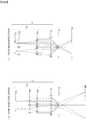
microscope apparatus 1 according to the present embodiment, theillumination apparatus 2 incorporated in thebase unit 101 of themicroscope apparatus 1 is configured, as shown inFigure 3 , such that thelight diffusing element 23, which diffuses the luminous flux transmitted without being shielded by thelight shielding plate 22, is arranged between the sample surface S and thelight shielding plate 22. Note that, inFigure 3 , reference character D denotes an optical-axis direction interval between thelight shielding plate 22 and thelight diffusing element 23. - In the microscope apparatus 1 having the illumination apparatus 2 configured in this way, when the light diffusing element 23 is arranged at a position α between the conjugate image PI of the entrance pupil and the sample surface S (a position near the sample surface S) as shown in
Figure 7 , light is diffused so that, as shown inFigure 7 , the conjugate image of the entrance pupil is not only formed on the one plane (the plane of the conjugate image PI of the entrance pupil which plane is formed when the light diffusing element 23 is not arranged) having the optical axis as a normal, but also formed, by the diffused light, on each of a plurality of planes represented by points A, B and C. On the other hand, as shown inFigure 8 , when the light diffusing element 23 is arranged at a position β (in a state of being close to the conjugate image PI of the entrance pupil) which is separated from the sample surface S by a greater distance than in the case shown inFigure 7 , the conjugate image of the entrance pupil is not only formed on the plane of the conjugate image PI of the entrance pupil, which plane is formed when the light diffusing element 23 is not arranged, but the conjugate image of the entrance pupil is also formed, by the diffused light, on each of a plurality of planes represented by points A', B' and C'. Note that inFigure 7 andFigure 8 , among rays emitted from the pupil (aperture stop 32c) of the imagingoptical system 3 toward the sample surface S, the rays corresponding to the maximum aperture are indicated by broken lines. Further, in the region extending from thelight diffusing element 23 inFigure 7 andFigure 8 , in addition to the rays corresponding to the maximum aperture, rays toward two directions are shown among the rays diffused from each of the rays corresponding to the maximum aperture. - As can be seen from
Figure 7 andFigure 8 , when thelight diffusing element 23 is arranged between the sample surface S and the conjugate image PI of the entrance pupil, and when thelight guide plate 21 and thelight shielding plate 22 are arranged at least between the points A to C (points A' to C'), the entrance pupil of the imagingoptical system 3 can be filled with the illumination light. That is, by providing thelight diffusing element 23, it is possible to obtain an effect as if the depth of focus of the conjugate image of the entrance pupil is increased. For this reason, when thelight guide plate 21 and thelight shielding plate 22 shown inFigure 3 are arranged in the range of the points A to C (points A' to C') in consideration of the magnification of theobjective lens 31 and of the variablepower lens group 32, the entrance pupil can be filled with the illumination light regardless of the magnification of the imagingoptical system 3. Further, thelight shielding plate 22, which is moved in one plane having the optical axis of theobjective lens 31 as a normal, similarly has the problem that the variable power range, in which the oblique illumination can be performed, is restricted because thelight shielding plate 22 cannot suitably restrict the conjugate image PI of the entrance pupil of the imagingoptical system 3, which conjugate image PI is moved according to the change in the magnification. However, in the case where thelight diffusing element 23 is provided as described above, even when the magnification of theobjective lens 31 and of the variablepower lens group 32 is changed, thelight guide plate 21 and thelight shielding plate 22 can be arranged in the range of the diffused conjugate images of the entrance pupil (the images formed in the points A to C, or the points A' to C'), and hence oblique illumination can be suitably performed. At this time, as shown inFigure 7 andFigure 8 , when thelight diffusing element 23 is arranged so as to be close to the sample surface S, the arrangement area of thelight guide plate 21 and thelight shielding plate 22 is expanded. Thus, such arrangement of thelight diffusing element 23 is preferred. - Further, as described above, when the light shielding plate having the transmittance of approximately 0% is used in the conventional microscope apparatus, there is a case where the contrast at the boundary portion of a phase object as a sample becomes too high and thereby the detailed structure around the boundary portion cannot be observed. However, when the light is transmitted through the
light diffusing element 23, the directivity of oblique illumination is weakened, so that, even when the light shielding plate having the transmittance of 0% is used, it is possible to suppress glare due to the excessive contrast of the observation image. - Here, it is preferred that the distance D [mm] between the light diffusing
element 23 and thelight shielding plate 22 satisfies the following expression (1).
- The thickness from the bottom portion of an ordinary illumination frame (for example, the
base unit 101 shown inFigure 1 ) to the sample surface is about 80 mm to 150 mm. On the other hand, the thickness of an illumination frame referred to as a thin type is 50 mm or less. In order to realize an illumination frame having a thickness of 50 mm or less, it should be configured such that the conjugate image PI of the entrance pupil of the imagingoptical system 3 is formed at a position separated by about 40 mm downward from the sample surface, and such that thelight shielding plate 22 and the light source (light guide plate 21) are arranged in the vicinity of the position. Further, in the stereoscopic microscope apparatus, the aperture of a 1×objective lens, which is most normally used, is in the range of 0.015 to 0.025 at the minimum magnification of the variable power lens. Since the optical system is considered to be almost free from aberration, the point image intensity distribution on the optical axis can be analytically calculated, and the intensity becomes 0 at a position separated by 2 mm to 6 mm from the position where the intensity becomes a maximum. Therefore, in order to prevent the formation of the sample image from being affected by the surface structure of thelight diffusing element 23, it is more preferred that thelight diffusing element 23 is arranged to be separated by 6 mm or more from the sample surface. However, because of the above-described reason, it is preferred that the interval D between the light diffusingelement 23 and thelight shielding plate 22 is 34 mm or less. - Meanwhile, it is known that, when the parallel transmittance and the haze value, as the optical properties of the diffusion surface of the
light diffusing element 23, are respectively set as T [%] and H [%], the parallel transmittance and the haze value respectively satisfy the conditions expressed by the following expressions (2) and (3).

- When the parallel transmittance T of the diffusion surface of the
light diffusing element 23 is less than the lower limit of the conditional expression (2), the secular deterioration of the light source by heat becomes a problem. On the contrary, when the parallel transmittance T of the diffusion surface of thelight diffusing element 23 exceeds the upper limit of the conditional expression (2), the directivity of oblique illumination is enhanced, so that it is not possible to suppress glare due to the excessive contrast of the observation image. Further, when the haze value H of the diffusion surface of thelight diffusing element 23 is less than the lower limit of the conditional expression (3), the above-described diffusion effect is lost. On the contrary, when the haze value H of the diffusion surface of thelight diffusing element 23 exceeds the upper limit of the conditional expression (3), the contrast cannot be given to the observation image of the phase object. Note that it is more preferred that thelight diffusing element 23 satisfies the following expressions (4) and (5).

- Note that, when a
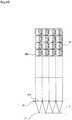
condenser lens 24 is added to theillumination apparatus 2 as shown inFigure 9(a) and Figure 9(b) , then in a wide variable power range from a low-power region to a high-power region of the low-power objective lens 31 and of the variablepower lens group 32, the conjugate image PI of the entrance pupil of the imagingoptical system 3 can be formed at an almost fixed position which is located on the illumination side with the sample surface as a boundary and which is close to the sample surface. Thus, when thelight guide plate 21 and thelight shielding plate 22 are arranged at the position of the conjugate image PI of the entrance pupil or at a position close to the position of the conjugate image PI of the entrance pupil, it is possible to realize a thin transmitted illumination optical system. In the case of such configuration, thelight diffusing element 23 is arranged between the sample surface S and the condenser lens. Further, in order to further reduce the thickness of the illumination optical system, it is effective to reduce the focal distance of thecondenser lens 24. However, thecondenser lens 24 is configured by a possible smallest number of lenses for the thickness reduction. Thus, when the focal distance is reduced, it becomes difficult to perform aberration correction. For this reason, in such case, the aberration correction effect can be given to thecondenser lens 24 by forming the surface shape of at least one surface of thecondenser lens 24 into an aspheric shape. - Further, when a
lens array 25, which is formed by arranging a plurality ofmicro lenses 25a in an array form as shown inFigure 10 , is used instead of thecondenser lens 24, the focal distance of the onemicro lens 25a can be reduced, and hence the thickness of theillumination apparatus 2 can be reduced. However, when oblique illumination is performed, it is necessary, as shown inFigure 10 , to shield the illumination light by using alight shielding plate 26 that is configured to shield each of the conjugate images PIa of the entrance pupil, which are formed by the number corresponding to the number of themicro lenses 25a. Note that, even in the case of such configuration, it is possible to adjust the visual field by inserting an adjustable diaphragm between the sample surface S and thelight shielding plate 22. Also, in this case, thelight diffusing element 23 is arranged between the sample surface S and the lens array. - Further, instead of the condenser lens and the light diffusing element, a condenser lens, at least one surface of which is a diffusion surface, may also be arranged. As a result, the number of elements is reduced by one, so that the thickness of the
illumination apparatus 2 can be further reduced. Further, when a weak phase object is observed, there is also a case where the observation is to be performed with high contrast. For this reason, it is also effective to enable thelight diffusing element 23 to be inserted and extracted into and from the optical path of theillumination apparatus 2. - Note that, in the configuration described above, even when the light source of the
light guide plate 21 is exchanged by the other light source, such as, for example, a cold cathode tube, or the like, such configuration is also included in the scope of the present invention utilizing the small thickness of the surface light emitter. Further, a configuration, in which a thin surface light source, such as organic EL, inorganic EL, and the like, is used instead of thelight guide plate 21, is also similarly included in the scope of the present invention. - Further, when bright field observation is performed in the
microscope apparatus 1, it is only necessary to completely remove thelight shielding plate 22 from the optical path. In this case, the bright field observation is not hindered, even when, in order to further reduce the thickness of theillumination apparatus 2, theillumination apparatus 2 is configured such that, as shown inFigure 3 , the condenser lens is removed to allow thelight guide plate 21 to be located directly under the sample surface S. In this case, it is possible to adjust the visual field by inserting an adjustable diaphragm between the sample surface S and thelight guide plate 21. However, when thelight guide plate 21 is arranged within the depth of focus of theobjective lens 31, there is a possibility that the structure in thelight guide plate 21 is seen and thereby the observation is hindered. Thus, when a low-power objective lens having a deep depth of focus is used as theobjective lens 31, it is preferred that theobjective lens 31 is arranged at a position away from the sample surface S. - 1 Microscope apparatus
- 2 Illumination apparatus
- 21 Light guide plate (surface light emitter)
- 21a Light emitting surface
- 22, 26 Light shielding plate (light shielding element)
- 23 Light diffusing element
- 24 Condenser lens
- 25 Lens array
- 25a Micro lens
- 3 Imaging optical system
- 31 Objective lens
- 32 Variable power lens group
- S Sample
- PI, PIa Conjugate image of entrance pupil of imaging optical system


Claims (11)
- A microscope apparatus (1)comprising:an illumination apparatus (2) which includes a surface light emitter (21) having a light emitting surface (21a) as a planar light-emitting region and irradiates a sample (S) with light emitted from the surface light emitter; andan imaging optical system (3) which includes an objective lens (31) configured to condense light from the sample, and a variable power lens group(32) configured to form an image of the sample and to change the magnification of the image,wherein the illumination apparatus includes a light diffusing element (23) which diffuses the light emitted from the light emitting surface,a light shielding element (22, 26) which is arranged at a position between the surface light emitter and the light diffusing element, and shields a part of a luminous flux emitted from the light emitting surface,wherein the light diffusing element (23) is arranged between the sample and a conjugate image (PI)of an entrance pupil of the imaging optical system, and the surface light emitter (21) and the light shielding element (22) are arranged in the range of the diffused conjugate images of the entrance pupil for all magnifications of the imaging optical system so that the entrance pupil can be filled with the illumination light regardless of the magnification of the imaging optical system.
- The microscope apparatus according to claim 1, wherein the illumination apparatus (2) is configured to be able to perform oblique illumination.
- The microscope apparatus according to claim 1 or claim 2, wherein, when the interval between the light shielding element (22, 26) and the light diffusing element (23) is set as D [mm], a condition given by the following expression is satisfied: D ≤ 34.
- The microscope apparatus according to one of claim 1 to claim 3, wherein, when the parallel light transmittance and the haze value which are optical properties of the diffusion surface formed in the light diffusing element is respectively set as T [%] and H [%], conditions given by the following expressions are satisfied: 50 < T < 95 and 10 < H < 98.
- The microscope apparatus according to one of claim 1 to claim 4, wherein the illumination apparatus includes a condenser lens (24) which condenses the light emitted from the surface light emitter and irradiates the sample with the condensed light.
- The microscope apparatus according to claim 5, wherein the condenser lens (24) includes at least one surface formed in an aspheric shape.
- The microscope apparatus according to claim 5, wherein the condenser lens (24) is configured by a lens array in which a plurality of lenses arranged in an array form.
- The microscope apparatus according to one of claim 1 to claim 7, wherein the surface light emitter (21)is configured by including a light source, and a light guide plate which includes a light emitting surface and allows light emitted from the light source to be emitted from the light emitting surface.
- The microscope apparatus according to claim 8, wherein the light source is configured by a plurality of white LEDs.
- The microscope apparatus according to claim 8, wherein the light source is configured by a plurality of LEDs each having a different peak wavelength.
- The microscope apparatus according to one of claim 1 to claim 10, wherein at least one of the surface light emitter (21) and the condenser lens (24) is configured to be movable along the optical axis.
Applications Claiming Priority (2)
| Application Number | Priority Date | Filing Date | Title |
|---|---|---|---|
| JP2009159483 | 2009-07-06 | ||
| PCT/JP2010/060706WO2011004714A1 (en) | 2009-07-06 | 2010-06-24 | Microscope |
Publications (3)
| Publication Number | Publication Date |
|---|---|
| EP2453284A1 EP2453284A1 (en) | 2012-05-16 |
| EP2453284A4 EP2453284A4 (en) | 2015-03-18 |
| EP2453284B1true EP2453284B1 (en) | 2020-10-21 |
Family
ID=43429137
Family Applications (1)
| Application Number | Title | Priority Date | Filing Date |
|---|---|---|---|
| EP10797025.3AActiveEP2453284B1 (en) | 2009-07-06 | 2010-06-24 | Microscope |
Country Status (5)
| Country | Link |
|---|---|
| US (1) | US8922886B2 (en) |
| EP (1) | EP2453284B1 (en) |
| JP (1) | JP5472831B2 (en) |
| CN (1) | CN102472888B (en) |
| WO (1) | WO2011004714A1 (en) |
Families Citing this family (11)
| Publication number | Priority date | Publication date | Assignee | Title |
|---|---|---|---|---|
| AU2003290094A1 (en) | 2003-10-29 | 2005-06-08 | Asml Netherlands B.V. | Optical assembly for photolithography |
| EP2764398A4 (en)* | 2011-10-06 | 2015-05-20 | Front Street Invest Man Inc As Manager For Front Street Diversified Income Class | Three dimensional stereoscopic microscope |
| US9250431B2 (en)* | 2013-09-05 | 2016-02-02 | Excelitas Canada, Inc. | Diffusing collection lens for direct coupled high power microscopy illumination systems |
| KR102058453B1 (en) | 2014-10-14 | 2019-12-23 | 나노트로닉스 이미징, 인코포레이티드 | Unique oblique lighting technique using a brightfield darkfield objective and imaging method relating thereto |
| TWI653465B (en) | 2014-10-24 | 2019-03-11 | 億觀生物科技股份有限公司 | Microscope module and microscope device |
| JP6482894B2 (en)* | 2015-02-19 | 2019-03-13 | オリンパス株式会社 | Microscope illumination device and microscope |
| JP6761330B2 (en)* | 2016-11-25 | 2020-09-23 | オリンパス株式会社 | Lighting equipment for microscopes and microscopes |
| CN106772995A (en)* | 2016-12-22 | 2017-05-31 | 广东清立方科技有限公司 | A kind of micrurgy 3D camera shooting integrated machines |
| DE102019130751A1 (en)* | 2019-11-14 | 2021-05-20 | Carl Zeiss Microscopy Gmbh | Lighting module for variable-angle lighting |
| CN111598058A (en)* | 2020-06-24 | 2020-08-28 | 无锡市科德科技有限公司 | A brightfield and darkfield directional reflection light source assembly based on a single light source |
| KR102223433B1 (en)* | 2020-11-24 | 2021-03-05 | 주식회사 트랙스원 | Digital microscope |
Family Cites Families (20)
| Publication number | Priority date | Publication date | Assignee | Title |
|---|---|---|---|---|
| JPH03223710A (en)* | 1989-12-13 | 1991-10-02 | Asahi Chem Ind Co Ltd | microscope |
| JPH03293311A (en)* | 1990-03-23 | 1991-12-25 | Asahi Chem Ind Co Ltd | translucent glass slide |
| JPH0495914A (en)* | 1990-08-08 | 1992-03-27 | Asahi Chem Ind Co Ltd | Translucent slide glass |
| JP4503716B2 (en) | 1997-08-29 | 2010-07-14 | オリンパス株式会社 | Microscope transmission illumination device |
| DE69836030T2 (en) | 1997-08-29 | 2007-01-11 | Olympus Optical Co., Ltd. | microscope |
| JPH11218690A (en)* | 1998-02-04 | 1999-08-10 | Olympus Optical Co Ltd | Microscope with vertical fluorescent illuminating optical system |
| US6992718B1 (en)* | 1998-08-31 | 2006-01-31 | Matsushita Electric Industrial Co., Ltd. | Illuminating apparatus, display panel, view finder, video display apparatus, and video camera mounting the elements |
| JP4595151B2 (en)* | 1999-12-28 | 2010-12-08 | 株式会社ニコン | Stereo microscope and transmission illumination device |
| JP2002189174A (en)* | 2000-12-20 | 2002-07-05 | Olympus Optical Co Ltd | Illuminator for microscope |
| EP1324362A3 (en)* | 2001-12-18 | 2005-04-06 | Polymatech Co., Ltd. | Film-integrated key top |
| JP2005017905A (en)* | 2003-06-27 | 2005-01-20 | Olympus Corp | Stereomicroscope |
| JP4445720B2 (en)* | 2003-07-11 | 2010-04-07 | オリンパス株式会社 | Stereoscopic transmission illumination device |
| JP2005181428A (en)* | 2003-12-16 | 2005-07-07 | Olympus Corp | Incident-light illuminator and microscope provided with the same |
| DE102004017694B3 (en)* | 2004-04-10 | 2005-09-15 | Schott Ag | Back lighting bright field illumination equipment for e.g. stereo microscope, has white organic light emitting diodes arranged on light area, and radiating units provided on light emitting side of functional layer |
| US7345815B2 (en)* | 2004-04-28 | 2008-03-18 | Olympus Corporation | Illumination apparatus for microscope |
| DE102005047593A1 (en)* | 2005-10-05 | 2007-04-12 | Carl Zeiss Jena Gmbh | Device for variation and adjustment of transmitted light illumination for microscopes |
| JP2007147743A (en)* | 2005-11-24 | 2007-06-14 | Nikon Corp | Microscope illumination device and microscope having the same |
| JP2007333800A (en)* | 2006-06-12 | 2007-12-27 | Nikon Corp | Microscope illumination device and microscope device having the same |
| CN101256277A (en)* | 2007-05-08 | 2008-09-03 | 杭州亿奥光电有限公司 | Non-contact type microscope bottom light source and power supply mode |
| DE102007047461A1 (en)* | 2007-09-28 | 2009-04-02 | Carl Zeiss Microimaging Gmbh | Method and optical arrangement for examining a sample |
- 2010
- 2010-06-24WOPCT/JP2010/060706patent/WO2011004714A1/enactiveApplication Filing
- 2010-06-24EPEP10797025.3Apatent/EP2453284B1/enactiveActive
- 2010-06-24CNCN201080030240.6Apatent/CN102472888B/enactiveActive
- 2010-06-24JPJP2011521880Apatent/JP5472831B2/enactiveActive
- 2011
- 2011-12-29USUS13/340,296patent/US8922886B2/enactiveActive
Non-Patent Citations (1)
| Title |
|---|
| None* |
Also Published As
| Publication number | Publication date |
|---|---|
| WO2011004714A1 (en) | 2011-01-13 |
| US8922886B2 (en) | 2014-12-30 |
| CN102472888B (en) | 2014-08-20 |
| JP5472831B2 (en) | 2014-04-16 |
| EP2453284A4 (en) | 2015-03-18 |
| US20120127569A1 (en) | 2012-05-24 |
| EP2453284A1 (en) | 2012-05-16 |
| CN102472888A (en) | 2012-05-23 |
| JPWO2011004714A1 (en) | 2012-12-20 |
Similar Documents
| Publication | Publication Date | Title |
|---|---|---|
| EP2453284B1 (en) | Microscope | |
| US10877256B2 (en) | Observation device | |
| EP1750154B1 (en) | Microscopic illumination apparatus | |
| US8837042B2 (en) | Transillumination device for a microscope | |
| US20190187450A1 (en) | Observation apparatus | |
| JP6913513B2 (en) | Lighting equipment for microscopes and microscopes | |
| CN113039470B (en) | Microscope device | |
| JP5567911B2 (en) | Illumination optical system and fluorescence microscope using the same | |
| CN204462528U (en) | Lighting device and stereomicroscope | |
| JP6140407B2 (en) | Microscope with transmitted light illuminator for critical illumination | |
| JP2012008361A (en) | Stereoscopic microscope | |
| JP2010060753A (en) | Microscope device | |
| JP2011095326A (en) | Illuminating apparatus for microscope | |
| US12235427B2 (en) | Observation apparatus | |
| JP5849540B2 (en) | Microscope illumination device and microscope | |
| JP2010156939A (en) | Illumination device and microscope device equipped with the same | |
| CA2653411A1 (en) | Dark field microscope and its adjusting method | |
| JP2002221664A (en) | Optical device and microscope | |
| EP3364226B1 (en) | Transmitted light illumination apparatus for a microscope | |
| JP2011209441A (en) | Microscope illuminator and microscope equipped with the same | |
| JP2016048394A (en) | Microscope illumination device and microscope | |
| CN116482849A (en) | General relief micro-imaging system based on oblique illumination | |
| JP2016151737A (en) | Microscope illumination device and microscope | |
| JP2005181428A (en) | Incident-light illuminator and microscope provided with the same | |
| PL187847B1 (en) | Stereoscopic microscope illuminator |
Legal Events
| Date | Code | Title | Description |
|---|---|---|---|
| PUAI | Public reference made under article 153(3) epc to a published international application that has entered the european phase | Free format text:ORIGINAL CODE: 0009012 | |
| 17P | Request for examination filed | Effective date:20111222 | |
| AK | Designated contracting states | Kind code of ref document:A1 Designated state(s):AL AT BE BG CH CY CZ DE DK EE ES FI FR GB GR HR HU IE IS IT LI LT LU LV MC MK MT NL NO PL PT RO SE SI SK SM TR | |
| DAX | Request for extension of the european patent (deleted) | ||
| A4 | Supplementary search report drawn up and despatched | Effective date:20150213 | |
| RIC1 | Information provided on ipc code assigned before grant | Ipc:G02B 21/22 20060101ALI20150209BHEP Ipc:G02B 21/06 20060101AFI20150209BHEP Ipc:G02B 21/08 20060101ALI20150209BHEP | |
| RAP1 | Party data changed (applicant data changed or rights of an application transferred) | Owner name:NIKON CORPORATION | |
| STAA | Information on the status of an ep patent application or granted ep patent | Free format text:STATUS: EXAMINATION IS IN PROGRESS | |
| 17Q | First examination report despatched | Effective date:20190408 | |
| GRAP | Despatch of communication of intention to grant a patent | Free format text:ORIGINAL CODE: EPIDOSNIGR1 | |
| STAA | Information on the status of an ep patent application or granted ep patent | Free format text:STATUS: GRANT OF PATENT IS INTENDED | |
| INTG | Intention to grant announced | Effective date:20200310 | |
| GRAS | Grant fee paid | Free format text:ORIGINAL CODE: EPIDOSNIGR3 | |
| GRAJ | Information related to disapproval of communication of intention to grant by the applicant or resumption of examination proceedings by the epo deleted | Free format text:ORIGINAL CODE: EPIDOSDIGR1 | |
| GRAL | Information related to payment of fee for publishing/printing deleted | Free format text:ORIGINAL CODE: EPIDOSDIGR3 | |
| STAA | Information on the status of an ep patent application or granted ep patent | Free format text:STATUS: EXAMINATION IS IN PROGRESS | |
| INTC | Intention to grant announced (deleted) | ||
| GRAR | Information related to intention to grant a patent recorded | Free format text:ORIGINAL CODE: EPIDOSNIGR71 | |
| STAA | Information on the status of an ep patent application or granted ep patent | Free format text:STATUS: GRANT OF PATENT IS INTENDED | |
| GRAA | (expected) grant | Free format text:ORIGINAL CODE: 0009210 | |
| STAA | Information on the status of an ep patent application or granted ep patent | Free format text:STATUS: THE PATENT HAS BEEN GRANTED | |
| AK | Designated contracting states | Kind code of ref document:B1 Designated state(s):AL AT BE BG CH CY CZ DE DK EE ES FI FR GB GR HR HU IE IS IT LI LT LU LV MC MK MT NL NO PL PT RO SE SI SK SM TR | |
| INTG | Intention to grant announced | Effective date:20200914 | |
| REG | Reference to a national code | Ref country code:GB Ref legal event code:FG4D | |
| REG | Reference to a national code | Ref country code:CH Ref legal event code:EP | |
| REG | Reference to a national code | Ref country code:DE Ref legal event code:R096 Ref document number:602010065734 Country of ref document:DE | |
| REG | Reference to a national code | Ref country code:IE Ref legal event code:FG4D | |
| REG | Reference to a national code | Ref country code:AT Ref legal event code:REF Ref document number:1326393 Country of ref document:AT Kind code of ref document:T Effective date:20201115 | |
| REG | Reference to a national code | Ref country code:AT Ref legal event code:MK05 Ref document number:1326393 Country of ref document:AT Kind code of ref document:T Effective date:20201021 | |
| REG | Reference to a national code | Ref country code:NL Ref legal event code:MP Effective date:20201021 | |
| PG25 | Lapsed in a contracting state [announced via postgrant information from national office to epo] | Ref country code:NO Free format text:LAPSE BECAUSE OF FAILURE TO SUBMIT A TRANSLATION OF THE DESCRIPTION OR TO PAY THE FEE WITHIN THE PRESCRIBED TIME-LIMIT Effective date:20210121 Ref country code:PT Free format text:LAPSE BECAUSE OF FAILURE TO SUBMIT A TRANSLATION OF THE DESCRIPTION OR TO PAY THE FEE WITHIN THE PRESCRIBED TIME-LIMIT Effective date:20210222 Ref country code:NL Free format text:LAPSE BECAUSE OF FAILURE TO SUBMIT A TRANSLATION OF THE DESCRIPTION OR TO PAY THE FEE WITHIN THE PRESCRIBED TIME-LIMIT Effective date:20201021 Ref country code:FI Free format text:LAPSE BECAUSE OF FAILURE TO SUBMIT A TRANSLATION OF THE DESCRIPTION OR TO PAY THE FEE WITHIN THE PRESCRIBED TIME-LIMIT Effective date:20201021 Ref country code:GR Free format text:LAPSE BECAUSE OF FAILURE TO SUBMIT A TRANSLATION OF THE DESCRIPTION OR TO PAY THE FEE WITHIN THE PRESCRIBED TIME-LIMIT Effective date:20210122 | |
| REG | Reference to a national code | Ref country code:LT Ref legal event code:MG4D | |
| PG25 | Lapsed in a contracting state [announced via postgrant information from national office to epo] | Ref country code:LV Free format text:LAPSE BECAUSE OF FAILURE TO SUBMIT A TRANSLATION OF THE DESCRIPTION OR TO PAY THE FEE WITHIN THE PRESCRIBED TIME-LIMIT Effective date:20201021 Ref country code:SE Free format text:LAPSE BECAUSE OF FAILURE TO SUBMIT A TRANSLATION OF THE DESCRIPTION OR TO PAY THE FEE WITHIN THE PRESCRIBED TIME-LIMIT Effective date:20201021 Ref country code:PL Free format text:LAPSE BECAUSE OF FAILURE TO SUBMIT A TRANSLATION OF THE DESCRIPTION OR TO PAY THE FEE WITHIN THE PRESCRIBED TIME-LIMIT Effective date:20201021 Ref country code:ES Free format text:LAPSE BECAUSE OF FAILURE TO SUBMIT A TRANSLATION OF THE DESCRIPTION OR TO PAY THE FEE WITHIN THE PRESCRIBED TIME-LIMIT Effective date:20201021 Ref country code:IS Free format text:LAPSE BECAUSE OF FAILURE TO SUBMIT A TRANSLATION OF THE DESCRIPTION OR TO PAY THE FEE WITHIN THE PRESCRIBED TIME-LIMIT Effective date:20210221 Ref country code:AT Free format text:LAPSE BECAUSE OF FAILURE TO SUBMIT A TRANSLATION OF THE DESCRIPTION OR TO PAY THE FEE WITHIN THE PRESCRIBED TIME-LIMIT Effective date:20201021 Ref country code:BG Free format text:LAPSE BECAUSE OF FAILURE TO SUBMIT A TRANSLATION OF THE DESCRIPTION OR TO PAY THE FEE WITHIN THE PRESCRIBED TIME-LIMIT Effective date:20210121 | |
| PG25 | Lapsed in a contracting state [announced via postgrant information from national office to epo] | Ref country code:HR Free format text:LAPSE BECAUSE OF FAILURE TO SUBMIT A TRANSLATION OF THE DESCRIPTION OR TO PAY THE FEE WITHIN THE PRESCRIBED TIME-LIMIT Effective date:20201021 | |
| REG | Reference to a national code | Ref country code:DE Ref legal event code:R097 Ref document number:602010065734 Country of ref document:DE | |
| PG25 | Lapsed in a contracting state [announced via postgrant information from national office to epo] | Ref country code:LT Free format text:LAPSE BECAUSE OF FAILURE TO SUBMIT A TRANSLATION OF THE DESCRIPTION OR TO PAY THE FEE WITHIN THE PRESCRIBED TIME-LIMIT Effective date:20201021 Ref country code:EE Free format text:LAPSE BECAUSE OF FAILURE TO SUBMIT A TRANSLATION OF THE DESCRIPTION OR TO PAY THE FEE WITHIN THE PRESCRIBED TIME-LIMIT Effective date:20201021 Ref country code:CZ Free format text:LAPSE BECAUSE OF FAILURE TO SUBMIT A TRANSLATION OF THE DESCRIPTION OR TO PAY THE FEE WITHIN THE PRESCRIBED TIME-LIMIT Effective date:20201021 Ref country code:SK Free format text:LAPSE BECAUSE OF FAILURE TO SUBMIT A TRANSLATION OF THE DESCRIPTION OR TO PAY THE FEE WITHIN THE PRESCRIBED TIME-LIMIT Effective date:20201021 Ref country code:RO Free format text:LAPSE BECAUSE OF FAILURE TO SUBMIT A TRANSLATION OF THE DESCRIPTION OR TO PAY THE FEE WITHIN THE PRESCRIBED TIME-LIMIT Effective date:20201021 Ref country code:SM Free format text:LAPSE BECAUSE OF FAILURE TO SUBMIT A TRANSLATION OF THE DESCRIPTION OR TO PAY THE FEE WITHIN THE PRESCRIBED TIME-LIMIT Effective date:20201021 | |
| PLBE | No opposition filed within time limit | Free format text:ORIGINAL CODE: 0009261 | |
| STAA | Information on the status of an ep patent application or granted ep patent | Free format text:STATUS: NO OPPOSITION FILED WITHIN TIME LIMIT | |
| PG25 | Lapsed in a contracting state [announced via postgrant information from national office to epo] | Ref country code:DK Free format text:LAPSE BECAUSE OF FAILURE TO SUBMIT A TRANSLATION OF THE DESCRIPTION OR TO PAY THE FEE WITHIN THE PRESCRIBED TIME-LIMIT Effective date:20201021 | |
| 26N | No opposition filed | Effective date:20210722 | |
| PG25 | Lapsed in a contracting state [announced via postgrant information from national office to epo] | Ref country code:AL Free format text:LAPSE BECAUSE OF FAILURE TO SUBMIT A TRANSLATION OF THE DESCRIPTION OR TO PAY THE FEE WITHIN THE PRESCRIBED TIME-LIMIT Effective date:20201021 Ref country code:IT Free format text:LAPSE BECAUSE OF FAILURE TO SUBMIT A TRANSLATION OF THE DESCRIPTION OR TO PAY THE FEE WITHIN THE PRESCRIBED TIME-LIMIT Effective date:20201021 | |
| PG25 | Lapsed in a contracting state [announced via postgrant information from national office to epo] | Ref country code:SI Free format text:LAPSE BECAUSE OF FAILURE TO SUBMIT A TRANSLATION OF THE DESCRIPTION OR TO PAY THE FEE WITHIN THE PRESCRIBED TIME-LIMIT Effective date:20201021 | |
| PG25 | Lapsed in a contracting state [announced via postgrant information from national office to epo] | Ref country code:MC Free format text:LAPSE BECAUSE OF FAILURE TO SUBMIT A TRANSLATION OF THE DESCRIPTION OR TO PAY THE FEE WITHIN THE PRESCRIBED TIME-LIMIT Effective date:20201021 | |
| REG | Reference to a national code | Ref country code:CH Ref legal event code:PL | |
| GBPC | Gb: european patent ceased through non-payment of renewal fee | Effective date:20210624 | |
| REG | Reference to a national code | Ref country code:BE Ref legal event code:MM Effective date:20210630 | |
| PG25 | Lapsed in a contracting state [announced via postgrant information from national office to epo] | Ref country code:LU Free format text:LAPSE BECAUSE OF NON-PAYMENT OF DUE FEES Effective date:20210624 | |
| PG25 | Lapsed in a contracting state [announced via postgrant information from national office to epo] | Ref country code:LI Free format text:LAPSE BECAUSE OF NON-PAYMENT OF DUE FEES Effective date:20210630 Ref country code:IE Free format text:LAPSE BECAUSE OF NON-PAYMENT OF DUE FEES Effective date:20210624 Ref country code:GB Free format text:LAPSE BECAUSE OF NON-PAYMENT OF DUE FEES Effective date:20210624 Ref country code:CH Free format text:LAPSE BECAUSE OF NON-PAYMENT OF DUE FEES Effective date:20210630 | |
| PG25 | Lapsed in a contracting state [announced via postgrant information from national office to epo] | Ref country code:IS Free format text:LAPSE BECAUSE OF FAILURE TO SUBMIT A TRANSLATION OF THE DESCRIPTION OR TO PAY THE FEE WITHIN THE PRESCRIBED TIME-LIMIT Effective date:20210221 Ref country code:FR Free format text:LAPSE BECAUSE OF NON-PAYMENT OF DUE FEES Effective date:20210630 | |
| PG25 | Lapsed in a contracting state [announced via postgrant information from national office to epo] | Ref country code:BE Free format text:LAPSE BECAUSE OF NON-PAYMENT OF DUE FEES Effective date:20210630 | |
| PG25 | Lapsed in a contracting state [announced via postgrant information from national office to epo] | Ref country code:HU Free format text:LAPSE BECAUSE OF FAILURE TO SUBMIT A TRANSLATION OF THE DESCRIPTION OR TO PAY THE FEE WITHIN THE PRESCRIBED TIME-LIMIT; INVALID AB INITIO Effective date:20100624 Ref country code:CY Free format text:LAPSE BECAUSE OF FAILURE TO SUBMIT A TRANSLATION OF THE DESCRIPTION OR TO PAY THE FEE WITHIN THE PRESCRIBED TIME-LIMIT Effective date:20201021 | |
| P01 | Opt-out of the competence of the unified patent court (upc) registered | Effective date:20230517 | |
| PG25 | Lapsed in a contracting state [announced via postgrant information from national office to epo] | Ref country code:MK Free format text:LAPSE BECAUSE OF FAILURE TO SUBMIT A TRANSLATION OF THE DESCRIPTION OR TO PAY THE FEE WITHIN THE PRESCRIBED TIME-LIMIT Effective date:20201021 | |
| PG25 | Lapsed in a contracting state [announced via postgrant information from national office to epo] | Ref country code:TR Free format text:LAPSE BECAUSE OF FAILURE TO SUBMIT A TRANSLATION OF THE DESCRIPTION OR TO PAY THE FEE WITHIN THE PRESCRIBED TIME-LIMIT Effective date:20201021 | |
| PG25 | Lapsed in a contracting state [announced via postgrant information from national office to epo] | Ref country code:MT Free format text:LAPSE BECAUSE OF FAILURE TO SUBMIT A TRANSLATION OF THE DESCRIPTION OR TO PAY THE FEE WITHIN THE PRESCRIBED TIME-LIMIT Effective date:20201021 | |
| PGFP | Annual fee paid to national office [announced via postgrant information from national office to epo] | Ref country code:DE Payment date:20250429 Year of fee payment:16 |