EP2448630B1 - Multi-element contact assemblies for electrical stimulation systems and systems and methods of making and using - Google Patents
Multi-element contact assemblies for electrical stimulation systems and systems and methods of making and usingDownload PDFInfo
- Publication number
- EP2448630B1 EP2448630B1EP10729008.2AEP10729008AEP2448630B1EP 2448630 B1EP2448630 B1EP 2448630B1EP 10729008 AEP10729008 AEP 10729008AEP 2448630 B1EP2448630 B1EP 2448630B1
- Authority
- EP
- European Patent Office
- Prior art keywords
- conductor
- lead
- conductors
- disposed
- inner element
- Prior art date
- Legal status (The legal status is an assumption and is not a legal conclusion. Google has not performed a legal analysis and makes no representation as to the accuracy of the status listed.)
- Active
Links
Images


Classifications
- A—HUMAN NECESSITIES
- A61—MEDICAL OR VETERINARY SCIENCE; HYGIENE
- A61N—ELECTROTHERAPY; MAGNETOTHERAPY; RADIATION THERAPY; ULTRASOUND THERAPY
- A61N1/00—Electrotherapy; Circuits therefor
- A61N1/02—Details
- A61N1/04—Electrodes
- A61N1/05—Electrodes for implantation or insertion into the body, e.g. heart electrode
- A—HUMAN NECESSITIES
- A61—MEDICAL OR VETERINARY SCIENCE; HYGIENE
- A61N—ELECTROTHERAPY; MAGNETOTHERAPY; RADIATION THERAPY; ULTRASOUND THERAPY
- A61N1/00—Electrotherapy; Circuits therefor
- A61N1/18—Applying electric currents by contact electrodes
- A61N1/32—Applying electric currents by contact electrodes alternating or intermittent currents
- A61N1/36—Applying electric currents by contact electrodes alternating or intermittent currents for stimulation
- A61N1/372—Arrangements in connection with the implantation of stimulators
- A61N1/375—Constructional arrangements, e.g. casings
- A61N1/3752—Details of casing-lead connections
- H—ELECTRICITY
- H01—ELECTRIC ELEMENTS
- H01R—ELECTRICALLY-CONDUCTIVE CONNECTIONS; STRUCTURAL ASSOCIATIONS OF A PLURALITY OF MUTUALLY-INSULATED ELECTRICAL CONNECTING ELEMENTS; COUPLING DEVICES; CURRENT COLLECTORS
- H01R13/00—Details of coupling devices of the kinds covered by groups H01R12/70 or H01R24/00 - H01R33/00
- H01R13/02—Contact members
- H01R13/22—Contacts for co-operating by abutting
- H01R13/24—Contacts for co-operating by abutting resilient; resiliently-mounted
- H01R13/2407—Contacts for co-operating by abutting resilient; resiliently-mounted characterized by the resilient means
- H01R13/2421—Contacts for co-operating by abutting resilient; resiliently-mounted characterized by the resilient means using coil springs
- H—ELECTRICITY
- H01—ELECTRIC ELEMENTS
- H01R—ELECTRICALLY-CONDUCTIVE CONNECTIONS; STRUCTURAL ASSOCIATIONS OF A PLURALITY OF MUTUALLY-INSULATED ELECTRICAL CONNECTING ELEMENTS; COUPLING DEVICES; CURRENT COLLECTORS
- H01R2107/00—Four or more poles
- H—ELECTRICITY
- H01—ELECTRIC ELEMENTS
- H01R—ELECTRICALLY-CONDUCTIVE CONNECTIONS; STRUCTURAL ASSOCIATIONS OF A PLURALITY OF MUTUALLY-INSULATED ELECTRICAL CONNECTING ELEMENTS; COUPLING DEVICES; CURRENT COLLECTORS
- H01R24/00—Two-part coupling devices, or either of their cooperating parts, characterised by their overall structure
- H01R24/58—Contacts spaced along longitudinal axis of engagement
Definitions
- the present descriptionis directed to the area of implantable electrical stimulation systems and methods of making and using the systems.
- the present descriptionis also directed to implantable electrical stimulation leads (and lead extensions) having multi-element contact assemblies, as well as methods of making and using the leads (and lead extensions), multi-element contact assemblies, and electrical stimulation systems.
- Implantable electrical stimulation systemshave proven therapeutic in a variety of diseases and disorders.
- spinal cord stimulation systemshave been used as a therapeutic modality for the treatment of chronic pain syndromes.
- Peripheral nerve stimulationhas been used to treat chronic pain syndrome and incontinence, with a number of other applications under investigation.
- Functional electrical stimulation systemshave been applied to restore some functionality to paralyzed extremities in spinal cord injury patients.
- a stimulatorcan include a control module (with a pulse generator), one or more leads, and an array of stimulator electrodes on each lead.
- the stimulator electrodesare in contact with or near the nerves, muscles, or other tissue to be stimulated.
- the pulse generator in the control modulegenerates electrical pulses that are delivered by the electrodes to body tissue.
- an implantable leadincludes a lead body having it distal end, a proximal end, and a longitudinal length.
- a plurality of electrodesare disposed on the distal end of the lead body.
- a plurality of terminalsare disposed on the proximal end of the lead body.
- a plurality of conductorsare disposed in the lead body such that each conductor electrically couples at least one of the electrodes to at least one of the terminals. At least one of the electrodes or at least one of the terminals includes a multi-element contact assembly.
- the multi-element contact assemblyincludes at least one conductive inner element and at least one conductive outer element disposed over the inner element. At least one of the plurality of conductors is electrically coupled to one of the multi-element contact assemblies such that the conductor is positioned against the at least one inner element.
- the at least one outer elementincludes a region that is in contact with the at least one inner element.
- a method for forming an implantable leadincludes disposing a plurality of elongated conductors in a lead body of the lead such that ends of the conductors extend from ends of the lead body.
- a multi-element contact assemblyis disposed at one of the ends of the lead body.
- the multi-element contact assemblyincludes an inner element and an outer element disposed over the inner element.
- An end of one of the plurality of conductorsis disposed into the multi-element contact assembly such that the conductor is positioned against the at least one inner element.
- a region of the at least one outer elementis contacted with the at least one inner element.
- a method for forming an implantable leadincludes disposing a plurality of elongated conductors in a lead body of the lead such that ends of the conductors extend from ends of the lead body.
- Each of the ends of the conductors extending from one end of the lead bodyare physically attached to one of a di fferent one of a plurality of inner elements.
- a different one of a plurality of outer elementsare disposed individually over each of the inner elements to form a plurality of multi-element contact assemblies.
- Each of the multi-element contact assembliesincludes a one of the outer elements disposed around a one of the inner elements.
- Each of the inner elements of the multi-element contact assembliesare contacted to the corresponding outer elements.
- the present descriptionis directed to the area of implantable electrical stimulation systems and methods of making and using the systems.
- the present descriptionis also directed to implantable electrical stimulation leads (and lead extensions) having multi-element contact assemblies, as well as methods of making and using the leads (and lead extensions), multi-element contact assemblies, and electrical stimulation systems.
- Suitable implantable electrical stimulation systemsinclude, but are not limited to, an electrode lead ("lead") with one or more electrodes disposed on a distal end of the lead and one or more terminals disposed on one or more proximal ends of the lead.
- Leadsinclude, for example, percutaneous leads, paddle leads, and cuff leads. Examples of electrical stimulation systems with leads are found in, for example, U.S. Patents Nos. 6,181,969 ; 6,516,227 ; 6,609,029 ; 6,609,032 ; and 6,741,892 ; and U.S.
- Patent US 7949395(10/353,101) , US7066028 (10/503,281) , 11/238,240 ; US 2007/0150036 11/319,291 ; US 2007/0161294 (11/327,880) ; US 2007/0219595 (11/375,638) ; US 7974706 (11/393,991) ; and US 7672734 (11/396,309) .
- FIG. 1illustrates schematically one embodiment of an electrical stimulation system 100.
- the electrical stimulation systemincludes a control module (e.g., a stimulator or pulse generator) 102, a paddle body 104, and at least one lead body 106 coupling the control module 102 to the paddle body 104.
- the paddle body 104 and the one or more lead bodies 106form a lead.
- the paddle body 104typically includes an array of electrodes 134.
- the control module 102typically includes an electronic subassembly 110 and an optional power source 120 disposed in a sealed housing 114.
- the control module 102typically includes a connector 144 ( Figure 2 and 3A , see also 322 and 350 of Figure 3B ) into which the proximal end of the one or more lead bodies 106 can be plugged to make an electrical connection via conductive contacts on the control module 102 and terminals ( e.g., 310 in Figure 3A and 336 of Figure 3B ) on each of the one or more lead bodies 106.
- the electrical stimulation systemcan include more, fewer, or different components and can have a variety of different configurations including those configurations disclosed in the electrical stimulation system references cited herein.
- the electrodes 134can be disposed in an array at or near the distal end of the lead body 106 forming a percutaneous lead, as illustrated in Figure 2 .
- a percutaneous leadmay be isodiametric along the length of the lead.
- one or more lead extensions 312can be disposed between the one or more lead bodies 106 and the control module 102 to extend the distance between the one or more lead bodies 106 and the control module 102 of the embodiments shown in Figures 1 and 2 .
- the electrical stimulation systems or components of the electrical stimulation systemincluding one or more of the lead bodies 106, the paddle body 104, and the control module 102, are typically implanted into the body of a patient.
- the electrical stimulation systemcan be used for a variety of applications including, but not limited to, brain stimulation, neural spinal cord stimulation, muscle and the like.
- the electrodes 134can be formed using any conductive, biocompatible material. Examples of suitable materials include metals, alloys, conductive polymers, conductive carbon, and the like, as well as combinations thereof.
- the number of electrodes 134 in the array of electrodes 134may vary. For example, there can be two, four, six, eight, ten, twelve, fourteen, sixteen, or more electrodes 134. As will be recognized, other numbers of electrodes 134 may also be used.
- the electrodes of the paddle body 104 or one or more lead bodies 106are typically disposed in, or separated by, a non-conductive, biocompatible material including, for example, silicone, polyurethane, polyetheretherketone ("PEEK”), epoxy, and the like or combinations thereof.
- the paddle body 104 and one or more lead bodies 106may be formed in the desired shape by any process including, for example, molding (including injection molding), casting, and the like. Electrodes and connecting wires can be disposed onto or within a paddle body either prior to or subsequent to a molding or casting process.
- the non-conductive materialtypically extends from the distal end of the lead to the proximal end of each of the one or more lead bodies 106.
- the non-conductive, biocompatible material of the paddle body 104 and the one or more lead bodies 106may be the same or different.
- the paddle body 104 and the one or more lead bodies 106may be a unitary structure or can be formed as two separate structures that are permanently or detachably coupled together.
- Terminalsare typically disposed at the proximal end of the one or more lead bodies 106 for connection to corresponding conductive contacts ( e . g ., 314 in Figure 3A and 340 of Figure 3B ) in connectors ( e.g., 144 in Figures 1-3A and 322 and 350 of Figure 3B ) disposed on, for example, the control module 102 (or to other devices, such as conductive contacts on a lead extension, an operating room cable, or an adaptor).
- Conductive wires(conductors) (not shown) extend from the terminals ( e .
- each terminale.g ., 310 in Figure 3A and 336 of Figure 3B
- the conductive wiresmay be embedded in the non-conductive material of the lead or can be disposed in one or more lumens (not shown) extending along the lead. In some embodiments, there is an individual lumen for each conductive wire. In other embodiments, two or more conductive wires may extend through a lumen.
- the one or more lumensmay be flushed continually, or on a regular basis, with saline, epidural fluid, or the like.
- the one or more lumenscan be permanently or removably sealable at the distal end.
- leadsare coupled to connectors disposed on control modules.
- a lead 308is shown configured and arranged for insertion to the control module 102.
- the connector 144includes a connector housing 302.
- the connector housing 302defines at least one port 304 into which a proximal end 306 of a lead 308 with terminals 310 can be inserted, as shown by directional arrow 312.
- the connector housing 302also includes a plurality of conductive contacts 314 for each port 304.
- the conductive contacts 314can be aligned with the terminals 310 on the lead 308 to electrically couple the control module 102 to the electrodes (134 of Figure 1 ) disposed at a distal end of the lead 308.
- Examples of connectors in control modulesare found in, for example, U.S. Patent No. 7,244,150 and U.S. Patent Application Serial No. US 8224450 (1/532,844)
- a connector 322is disposed on a lead extension 324.
- the connector 322is shown disposed at a distal end 326 of the lead extension 324.
- the connector 322includes a connector housing 328.
- the connector housing 328defines at least one port 330 into which a proximal end 332 of a lead 334 with terminals 336 can be inserted, as shown by directional arrow 338.
- the connector housing 328also includes a plurality of conductive contacts 340.
- the conductive contacts 340 disposed in the connector housing 328can be aligned with the terminals 336 on the lead 334 to electrically couple the lead extension 324 to the electrodes (134 of Figure 1 ) disposed at a distal end (not shown) of the lead 334.
- the proximal end of a lead extensionis similarly configured and arranged as a proximal end of a lead.
- the lead extension 324may include a plurality of conductive wires (not shown) that electrically couple the conductive contacts 340 to a proximal end 348 of the lead extension 324 that is opposite to the distal end 326.
- the conductive wires disposed in the lead extension 324can be electrically coupled to a plurality of terminals (not shown) disposed on the proximal end 348 of the lead extension 324.
- the proximal end 348 of the lead extension 324is configured and arranged for insertion into a connector disposed in another lead extension.
- the proximal end 348 of the lead extension 324is configured and arranged for insertion into a connector disposed in a control module.
- the proximal end 348 of the lead extension 324is inserted into a connector 350 disposed in a control module 352.
- One or more of the conductors connecting at least one terminal to an electrodecan be arranged in a conductor path to eliminate or reduce the effect of RF irradiation, such as that generated during magnetic resonance imaging ("MRF").
- the conductor pathincludes a plurality of units arranged in series. In some embodiments, the units are disposed along a single continuous conductor. In other embodiments, the units are separate conductive elements electrically coupled together.
- Each unitincludes at least three conductor segments that at least partially overlap one another to form a multi-coil region.
- each unitincludes a first conductor segment that extends in a first direction along a longitudinal length of an elongated member (e.g., a lead or lead extension) from a beginning point to a first position.
- each unitincludes a second conductor segment that extends from the first position back towards (and possibly past) the beginning point to a second position.
- each unitincludes a third conductor segment that extends in the first direction from the second position to an endpoint.
- the first positionis between the second position and the endpoint.
- the second positionis between the beginning point and the first position.
- the unitmay include a single-coil region flanking at least one end of the multi-coil region.
- the unitsmay be electrically continuous such that the endpoint of a first unit is the beginning point of the next consecutive unit. At least one of the beginning points may be a terminal or an electrode (or other conductive contact). Likewise, at least one of the endpoints may be a terminal or an electrode (or other conductive contact).
- the conductor segmentsare each coiled. In at least some embodiments, the conductor segments are coiled around a conductor placement sleeve. In at least some embodiments, the conductor placement sleeve defines a lumen that optionally is configured and arranged to receive a stiffening member (e.g. , a stylet, or the like).
- At least one of the first, second, or third conductor segmentsis substantially straight. In at least some embodiments, the first and third conductor segments are substantially straight and the second conductor segment is coiled. In at least some other embodiments, all three conductor segment are substantially straight. It will be understood that the term “substantially straight conductor segment” means that the conductor segment is not coiled. A “substantially straight conductor segment” may be curved, particularly when the lead itself is curved (see, for example, Figure 1 ).
- the conductor segmentsare all formed from the same length of conductive material (e.g., wire or the like).
- the conductorsmay have a single filament or be multi-filar. In preferred embodiments, the conductors are multi-filar.
- two or more of the conductor segmentscan be individual pieces of conductive material that are electrically coupled ( e.g., soldered or welded) together.
- a layer of insulation(“conductors insulation'') is disposed over each of the conductor segments.
- the length of conductor used in the second conductor segmentis at least 1.5, 1.75, 1.9, 2, 2.1, 2.25, or 2.5 times the length of either the first conductor segment or the third conductor segment. It will be recognized, however, that this ratio of conductor-segment lengths may vary among embodiments, particularly if the thickness of the conductor or thickness of the layer of conductor insulation is different for the different segments.
- Figure 4schematically illustrates one embodiment of a plurality of conductors 402.
- the conductors 402are configured into a plurality of units, such as unit 404.
- Each unitincludes a first conductor segment 404a, a second conductor segment 404b, and a third conductor segment 404c.
- conductor insulationis disposed over the conductors 402 to electrically isolate each of the conductors 402 from one another.
- the conductors 402may be disposed along longitudinal lengths of the conductors 402 including, for example, two, three, four, five, six, seven, eight, nine, ten, twelve, fifteen, twenty, twenty-five, thirty, forty, fifty, or more units. It will be understood that many other numbers of units may be employed as well.
- the plurality of unitsWhen a plurality of units are coupled together in series along a longitudinal length of one or more conductors, the plurality of units form a repeating series of single-coil regions, such as the single-coil regions 406, separated from one another by a multi-coil region, such as the multi-coil region 408.
- the conductors 402are disposed along a conductor placement sleeve 410.
- the conductor placement sleeve 410can be formed from any suitable biocompatible material including, for example, one or more polymers.
- conductor insulationis disposed over the conductors 402 to encapsulate the conductors 402 and electrically isolate the conductors 402 from one another.
- one or more conductors having one or more unitsmay be disposed in an elongated member (e.g., a lead or lead extension).
- the ends of the conductors 402can be coupled to terminals, electrodes, or conductive contacts.
- each of the conductors in an elongated memberare configured into units.
- only a subset of the conductors disposed in an elongated memberinclude one or more units, the remaining conductors having a different arrangement (for example, a single conductor segment between the terminal(s) and electrode(s)/conductive contact(s)).
- Conductorssuch as the conductors 402, may be disposed in a lumen of an elongated member (e.g. , a lead, lead extension, or the like).
- Figure 5is a schematic longitudinal cross-sectional view of one embodiment of portions of a plurality of conductors 502 disposed in an elongated member 504.
- the illustrated portions of the conductors 502includes unit 506, shown between two vertical dotted lines.
- Unit 506includes a first conductor segment 506a, a second conductor segment 506b, and a third conductor segment 506c.
- the conductors 502are disposed over a conductor placement sleeve 508.
- the conductor placement sleeve 508defines a lumen 510.
- the elongated member 504includes a body 512 and a lumen 514 into which the conductors 502 are disposed.
- Figure 6Aschematically illustrates a side view of one embodiment of a plurality of conductors 602 each including units 604 and 606.
- the first, second, and third conductor segments 604a, 604b (not shown in Figure 6A ), and 604c, respectively, of the unit 604, and the first, second, and third conductor segments 606a, 606b (not shown in Figure 6A ), and 606c, respectively, of the unit 606,are each coiled.
- the conductors 602are arranged such that the conductors include multi-coil regions 608 and single-coil regions 610.
- the conductors 602may be coiled around one or more objects, such as a conductor placement sleeve 612.
- Figure 6Bis a schematic longitudinal cross-sectional view of the plurality of conductors 602 disposed in an outer layer 614 of a body 615 of a lead 616.
- outer layer 614 of the body 615is isodiametric along the longitudinal length of the lead 616, open spaces 618 may form between the single-coil regions, such as single-coil region 606a, and the outer layer 614.
- one or more contactsare disposed at opposing ends of an elongated member (e.g., a lead, a lead extension, or the like).
- the contacts disposed on opposite ends of the elongated memberare electrically coupled together by elongated conductors extending along a longitudinal length of the elongated member.
- terminals disposed on a proximal end of the conductormay be coupled, via conductors, to electrodes (or connective contacts) disposed on a distal end of the elongated member.
- the conductorsmay be disposed along a body of the elongated member in any number of different arrangements including, for example, configured into one or more units (as described above with reference to Figures 4-6B ), wrapped around a sleeve or mandrel, extending substantially straight, disposed in one or more conductor-carrying elements, or the like).
- connections between the conductors and the contactsbe strong enough to maintain a viable electrical connection during implantation and throughout the operational life of the electrical stimulation system within a patient.
- a loss of electrical connection between a conductor and a contactmay result in a loss of therapeutic stimulation and may even necessitate an undesired explanation of the electrical stimulation system from the patient.
- connection between the conductor and the contactis sometimes made by a heat-related method of coupling (e.g., laser welding, resistance welding, brazing, soldering, or the like).
- a heat-related method of coupling alonemay not provide sufficient strength to maintain an electrical connection between the conductor and the contact throughout the operational life of the electrical stimulation system.
- the conductormay also be mechanically clamped to the contact.
- Heat produced by the heat-related method of couplingtypically anneals the contact in a region of the contact in immediate proximity to the site of the heat-related coupling. The annealing may reduce the tensile strength of the conductor.
- One known attempt to separate the mechanical clamping from the heat-related couplinginvolved crimping sleeves to the ends of conductors, and then coupling the sleeves to the contacts, Unfortunately manufacturing and handling sleeves that are small enough for clamping to the ends of conductors is tedious and complex.
- contact assembliesare employed to electrically couple with contacts.
- the contact assembliesinclude a rigid (or semi-rigid), cylindrically-shaped outer element and a rigid (or semi-rigid) inner element that is disposed in the outer element.
- the inner elementis disposed concentrically in the outer element.
- the contactselectrically couple to the contact assemblies by positioning the conductors against the inner elements and contacting the outer elements and the inner elements.
- the outer elementsare mechanically deformed to electrically couple the conductors to at least one of the inner elements or the outer elements.
- the conductorsare also electrically coupled to the contact assemblies by physically attaching the conductors to the contact assemblies.
- the conductorsare physically attached to the contact assemblies by one or more heat-related coupling methods.
- both inner elements and outer elementsare formed from conductive materials.
- a contact assemblyis positioned at an end of a body of an elongated member and one of the conductors is positioned in the contact assembly such that the conductor is either internal or external to the inner element.
- the outer elementis mechanically deformed ( e . g ., bent, crimped, swaged, folded, creased, or the like) to press against one or more of the conductor and the inner element, thereby electrically coupling the conductor to at least one of the inner element or the outer element.
- the conductoris also physically attached to one or more of the inner element or the outer element by a heat-related method of coupling (e.g., laser welding, resistance welding, brazing, soldering, or the like), either before or after the outer element is mechanically deformed.
- a heat-related method of couplinge.g., laser welding, resistance welding, brazing, soldering, or the like
- the outer element and the inner elementare physically attached together (e.g., by a heat-related coupling method) after the outer element is mechanically deformed.
- conductorsmay be disposed along the body of the elongated member in any number of different arrangements including, for example, configured into one or more units, wrapped around a sleeve or mandrel, extending substantially straight, disposed in one or more conductor-carrying elements, or the like. It will be understood that, when one or more conductors are coiled ( e.g., configured into one or more units, or the like), the coils may extend to the electrodes, terminals, or both.
- a conductor-carrying elementmay be used to retain one or more conductors along at least a portion of an elongated member.
- Figure 7Ais a schematic end view of one embodiment of a conductor-carrying element 702 that includes multiple lumens.
- the conductor-carrying element 702defines a central lumen 704 and conductor lumens 706-713.
- the conductor-carrying element 702may include many different configurations and many different numbers and sizes of conductor lumens.
- one or more conductorsextend along at least a portion of a longitudinal length of the lead body within one of the conductor lumens 706-713. In at least some embodiments, ends of the conductors extend from an end of the conductor-carrying element 702.
- Figure 7Bis a schematic end view of one embodiment of the conductors 720-727 disposed in the conductor-carrying element 702. In at least some embodiments, insulation 730 is disposed around a longitudinal length of one or more of the conductors 720-727. Ends of the conductors 720-727 extend from the end of the conductor-carrying element 702.
- the extending ends of the conductors 720-727 on one end of the conductor-carrying element 702are typically coupled to terminals and the extending ends of the conductors 720-727 on the other end of the conductor-carrying element 702 are typically coupled to electrodes (or connector contacts).
- a contact assemblymay be disposed at one end of the conductor-carrying element 702 which, in turn, may be disposed in a lead body or a lead extension body.
- the end of one of the conductors 720-727 extending from the conductor-carrying element 702may be coupled to the conductor assembly.
- Figures 7B-9Bshow conductors extending along lumens defined in conductor-carrying elements.
- the conductor-carrying element 702extends the entire length of a lead body (or a lead extension body). In other embodiments, one or more conductor-carrying elements extend along portions of the length of a lead body (or a lead extension body). In at least some embodiments, a lead body (or a lead extension body) also includes one or more outer layers disposed over the one or more conductor-carrying elements. In at least some embodiments, contact assemblies are coupled with conductors that extend along lead bodies (or lead extension bodies) that do not include conductor-carrying elements.
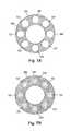
- Figures 8A and 8Bare schematic end and side views, respectively, of one embodiment of a first contact assembly 802 disposed at one end of the conductor-carrying element 702.
- the first contact assembly 802includes an inner element 804 and an outer element 806.
- the outer element 806functions as a contact (e.g., a terminal, an electrode, or the like).
- the leadis isodiametric. Accordingly, in at least some embodiments, the outer element 806 has a diameter that is equal to a diameter of a lead body (or a lead extension body). In at least some embodiments, the inner element 804 has a diameter that is equal to the diameter of the conductor-carrying element 702.
- the inner element 804 and the outer element 806can be formed using any rigid or semi-rigid, conductive, biocompatible material.
- suitable materialsinclude platinum, iridium, platinum iridium, titanium, alloys of any of the above-listed metals, super alloys ( e.g., MP35N and the like), stainless steel, and the like, as well as combinations thereof. It will be understood that the inner element 804 and the outer element 806 may be formed from either the same material or different materials.
- the inner element 804is disposed within the outer element 806 such that the inner element 804 and the outer elements 806 are concentric to one another.
- the outer element 806is cylindrical.
- the inner element 804is also cylindrical,
- the inner element 804is C-shaped.
- the outer element 806is C-shaped.
- the first contact assembly 802is disposed at one end of the conductor-carrying element 702.
- one of the conductors 720-727 extending from the end of the conductor-carrying element 702is coupled to the first contact assembly 802 and the remaining conductors 720-727 are extended through the inner element 804.
- the remaining conductor 720-727 that extend through the first contact assembly 802are coupled to one or more additional contacts subsequently positioned laterally from the first contact assembly 802.
- Figure 8B and in other figuresonly a few conductors are shown to represent the conductors 721-727, for clarity of illustration.
- conductor 720is shown coupled to the first contact assembly 802.
- the conductor 720is positioned against the inner element 804 such that the conductor 720 is disposed external to the inner element 804 and internal to the outer element 806.
- the outer element 806is deformed ( e . g ., mechanically deformed) to press the conductor 720 against at least one of the inner element 804 or the outer element 806, thereby electrically coupling the conductor 720 to at least one of the inner element 804 or the outer element 806.
- the outer element 806is mechanically deformed ( e . g ., bent, crimped, swaged, folded, creased, or the like).
- the conductor 720is positioned against the inner element 804 such that the conductor 720 is disposed internal to the inner element 804.
- the conductor 720is also electrically coupled to one or more of the inner element 804 or the outer element 806 by physically attaching the conductor 720 to one or more of the inner element 804 or the outer element 806. In at least some embodiments, the conductor 720 is physically attached to one or more of the inner element 804 or the outer element 806 by a heat-related method of attachment (e.g., laser welding, resistance welding, brazing, soldering, or the like).
- a heat-related method of attachmente.g., laser welding, resistance welding, brazing, soldering, or the like.
- the conductor 720may be electrically coupled, via the heat-related method of coupling, to one or more of the inner element 804 or the outer element 806 either before or after the conductor 720 is electrically coupled to one or more of the inner element 804 or the outer element 806 by mechanical deformation of the outer element 806.
- the inner element 804 and the outer element 806are coupled together, via the heat-related method of coupling, after the conductor 720 is electrically coupled to one or more of the inner element 804 or the outer element 806 by mechanical deformation of the outer element 806.
- insulation 730may be disposed over the longitudinal length of one or more of the conductors 720-727.
- the insulation 730 of the conductor 720is removed over at least a portion of the region of the conductor 720 coupled to the first contact assembly 802 prior to mechanical deformation of the outer element 806.
- the mechanical deformation processremoves enough of the insulation 730 to provide adequate electrical connection between the conductor 720 and at least one of the inner element 804 or the outer element 806 without needing to remove a portion of the insulation 730 prior to performing the mechanical deformation process.
- a spacer 808may be positioned adjacent to a second end of the first contact assembly 802 opposite to the first end.
- the conductors 721-727 extending through the inner element 804 of the contact assembly 802also extend through the spacer 808.
- the tip of the conductor 720may be removed or bent so that the tip of the conductor 720 does not obstruct the spacer 808 from abutting the first contact assembly 802.
- An additional contact assemblymay be positioned at the opposite end of the spacer from the first contact assembly and another conductor may be coupled to the additional contact assembly. It will be understood that any number of contact assemblies may be coupled to conductors and separated from one another by spacers. In at least some embodiments, the number of contact assemblies is equal to the number of conductors. It will further be understood that the same process may be repeated on an opposing end of the conductor-carrying element 702.
- Figure 8Cis a schematic side view of one embodiment of a second contact assembly 820 disposed at one end of the conductor-carrying element 702.
- the conductor 721is positioned between, and electrically coupled to, an inner element 822 and an outer element 824 of the second contact assembly 820.
- the remaining conductors 722-727extend through the inner element 822.
- the spacer 808separates the first contact assembly 802 from the second contact assembly 820.
- the outer elements 806 and 824both function as terminals or both function as electrodes. In preferred embodiments, if one or more additional contact assemblies are disposed on the same end of the conductor-carrying element 702 and separated from one another by spacers, the outer element(s) of those additional contact assemblies also function as outer elements 806 and 824. In at least some embodiments, one or more contact assemblies disposed on the opposite end of the conductor-carrying element 702 each have outer elements that function as the other of either terminals or electrodes, depending on the functionality of the outer elements 806 and 824.
- a conductoris physically attached to a C-shaped inner element via a heat-related method of coupling.
- An outer elementis then disposed over the inner element (and the electrically coupled conductor), and at least a portion of the outer element and the inner element are physically attached together.
- the inner elementis substantially flat when the conductor is physically attached to the inner element. In which case, the inner element is bent into a "C'" shape after the physical attachment of the conductor to the inner element.
- the conductoris electrically coupled to an inner surface of the inner element. In other embodiments, the conductor is electrically coupled to an outer surface of the inner element.
- Figure 9Ais a schematic end view of one embodiment of a contact assembly 902 disposed at one end of a conductor-carrying element 904.
- the contact assembly 902includes a C-shaped inner element 906 and a cylindrical outer element 908.
- Conductors, such as conductor 910,are disposed in the conductor-carrying element 904.
- Figure 9Bis a schematic side view of one embodiment of the contact assembly 902 disposed at one end of the conductor-carrying element 904 and the conductor 910 coupled to the inner element 906 which, in turn, is coupled to the outer element 908.
- the diameter of the outer element 908is equal to the diameter of a lead body (or lead extension body) in which the conductor-carrying element 904 is disposed.
- the conductor 910is shown electrically coupled to an inner surface 912 of the inner element 906. It will be understood that the conductor 910 may, instead, be electrically coupled to an outer surface of the inner element 906.
- the outer element 908is disposed over the inner element 906 such that the inner element 906 is compressed within the outer element 908.
- the outer element 908is electrically coupled to the inner element 906.
- the outer element 908is mechanically deformed to press against the inner element 906.
- the outer elementis physically attached to the inner element 906 by a heat-related method of coupling (e . g ., laser welding, resistance welding, brazing, soldering, or the like).
- the outer element 908 and the inner element 906are electrically coupled by both mechanical deformation of the outer element 908 and physical attachment.
- each of the conductors of the conductor-carrying element 904are physically attached to a different inner element.
- the inner elementsare arranged along an axis of the end of the conductor-carrying element 904 such that the conductors coupled to the more lateral inner elements extend through each of the more medial inner elements.
- Outer elementsare positioned over, and electrically coupled to, each inner element.
- at least one of the elementsmay be closed to form a continuous transverse path.
- the inner element 906has a longitudinal length 914 (shown in Figure 9B as a two-headed arrow) that is not equal to a longitudinal length 916 (also shown in Figure 9B as a two-headed arrow) of the outer element 908.
- the longitudinal length 916 of the outer element 908is greater than the longitudinal length 914 of the inner element 906. It may be an advantage to have the outer element 908 of the contact assembly 902 being greater in length than the inner element 906 so that, when the conductor 910 is coupled to the inner element 906, but not yet coupled to the outer element 908, the axial positioning of the inner element 906 may be adjusted without needing to axially adjust the outer element 908.
- the outer element 908may be positioned as desired without needing to axially adjust the outer element 908 to accommodate the positioning of the electrical coupling of the outer element 908 with the conductor 910.
- FIG 10is a schematic overview of one embodiment of components of an electrical stimulation system 1000 including an electronic subassembly 1010 disposed within a control module. It will be understood that the electrical stimulation system can include more, fewer, or different components and can have a variety of different configurations including those configurations disclosed in the simulator references cited herein.
- power source 1012can be used including, for example, a battery such as a primary battery or a rechargeable battery.
- a batterysuch as a primary battery or a rechargeable battery.
- other power sourcesinclude super capacitors, nuclear or atomic batteries, mechanical resonators, infrared collectors, thermally-powered energy sources, flexural powered energy sources, bioenergy power sources, fuel cells, bioelectric cells, osmotic pressure pumps, and the like including the power sources described in U.S. Patent Application Publication No. 2004/0059392 .
- powercan be supplied by an external power source through inductive coupling via the optional antenna 1018 or a secondary antenna.
- the external power sourcecan be in a device that is mounted on the skin of the user or in a unit that is provided near the user on a permanent or periodic basis.
- the batterymay be recharged using the optional antenna 1018, if desired. Power can be provided to the battery for recharging by inductively coupling the battery through the antenna to a recharging unit 1016 external to the user. Examples of such arrangements can be found in the references identified above.
- electrical currentis emitted by the electrodes 134 on the paddle or lead body to stimulate nerve fibers, muscle fibers, or other body tissues near the electrical stimulation system.
- a processor 1004is generally included to control the timing and electrical characteristics of the electrical stimulation system. For example, the processor 1004 can, if desired, control one or more of the timing, frequency, strength, duration, and waveform of the pulses. In addition, the processor 1004 can select which electrodes can be used to provide stimulation, if desired. In some embodiments, the processor 1004 may select which electrode(s) are cathodes and which electrode(s) are anodes. In some embodiments, the processor 1004 may be used to identify which electrodes provide the most useful stimulation of the desired tissue.
- Any processorcan be used and can be as simple as an electronic device that, for example, produces pulses at a regular interval or the processor can be capable of receiving and interpreting instructions from an external programming unit 1008 that, for example, allows modification of pulse characteristics.
- the processor 1004is coupled to a receiver 1002 which, in turn, is coupled to the optional antenna 1018. This allows the processor 1004 to receive instructions from an external source to, for example, direct the pulse characteristics and the selection of electrodes, if desired.
- the antenna 1018is capable of receiving signals (e.g., RF signals) from an external telemetry unit 1006 which is programmed by a programming unit 1008.
- the programming unit 1008can be external to, or part of, the telemetry unit 1006.
- the telemetry unit 1006can be a device that is worn on the skin of the user or can be carried by the user and can have a form similar to a pager, cellular phone, or remote control, if desired.
- the telemetry unit 1006may not be worn or carried by the user but may only be available at a home station or at a clinician's office,
- the programming unit 1008can be any unit that can provide information to the telemetry unit 1006 for transmission to the electrical stimulation system 1000.
- the programming unit 1008can be part of the telemetry unit 1006 or can provide signals or information to the telemetry unit 1006 via a wireless or wired connection.
- One example of a suitable programming unitis a computer operated by the user or clinician to send signals to the telemetry unit 1006.
- the signals sent to the processor 1004 via the antenna 1018 and receiver 1002can be used to modify or otherwise direct the operation of the electrical stimulation system.
- the signalsmay be used to modify the pulses of the electrical stimulation system such as modifying one or more of pulse duration, pulse frequency, pulse waveform, and pulse strength.
- the signalsmay also direct the electrical stimulation system 1000 to cease operation, to start operation, to start charging the battery, or to stop charging the battery.
- the stimulation systemdoes not include an antenna 1018 or receiver 1002 and the processor 1004 operates as programmed.
- the electrical stimulation system 1000may include a transmitter (not shown) coupled to the processor 1004 and the antenna 1018 for transmitting signals back to the telemetry unit 1006 or another unit capable of receiving the signals.
- the electrical stimulation system 1000may transmit signals indicating whether the electrical stimulation system 1000 is operating properly or not or indicating when the battery needs to be charged or the level of charge remaining in the battery.
- the processor 1004may also be capable of transmitting information about the pulse characteristics so that a user or clinician can determine or verify the characteristics.
Landscapes
- Health & Medical Sciences (AREA)
- Engineering & Computer Science (AREA)
- Biomedical Technology (AREA)
- Nuclear Medicine, Radiotherapy & Molecular Imaging (AREA)
- Radiology & Medical Imaging (AREA)
- Life Sciences & Earth Sciences (AREA)
- Animal Behavior & Ethology (AREA)
- General Health & Medical Sciences (AREA)
- Public Health (AREA)
- Veterinary Medicine (AREA)
- Cardiology (AREA)
- Heart & Thoracic Surgery (AREA)
- Electrotherapy Devices (AREA)
Description
- The present description is directed to the area of implantable electrical stimulation systems and methods of making and using the systems. The present description is also directed to implantable electrical stimulation leads (and lead extensions) having multi-element contact assemblies, as well as methods of making and using the leads (and lead extensions), multi-element contact assemblies, and electrical stimulation systems.
- Implantable electrical stimulation systems have proven therapeutic in a variety of diseases and disorders. For example, spinal cord stimulation systems have been used as a therapeutic modality for the treatment of chronic pain syndromes. Peripheral nerve stimulation has been used to treat chronic pain syndrome and incontinence, with a number of other applications under investigation. Functional electrical stimulation systems have been applied to restore some functionality to paralyzed extremities in spinal cord injury patients.
- Stimulators have been developed to provide therapy for a variety of treatments. A stimulator can include a control module (with a pulse generator), one or more leads, and an array of stimulator electrodes on each lead. The stimulator electrodes are in contact with or near the nerves, muscles, or other tissue to be stimulated. The pulse generator in the control module generates electrical pulses that are delivered by the electrodes to body tissue.
- Conventional implanted electrical stimulation systems are often incompatible with magnetic resonance imaging ("MRI") due to the large radio frequency ("RF") pulses used during MRI. The RF pulses can generate transient signals in the conductors and electrodes of an implanted lead. These signals can have deleterious effects including, for example, unwanted heating of the tissue causing tissue damage, induced currents in the lead, or premature failure of electronic components.
US-2004/0106964 discloses an implantable electrode comprising a conductor that contacts an inner ring and an outer ring placed over the conductor and the inner ring. - The present invention is as set out in the appended claims that follow. The examples, embodiments or aspects of the present description that do not fall within the scope of said claims are provided for illustrative purposes only and do not form part of the present invention. In one embodiment, an implantable lead includes a lead body having it distal end, a proximal end, and a longitudinal length. A plurality of electrodes are disposed on the distal end of the lead body. A plurality of terminals are disposed on the proximal end of the lead body. A plurality of conductors are disposed in the lead body such that each conductor electrically couples at least one of the electrodes to at least one of the terminals. At least one of the electrodes or at least one of the terminals includes a multi-element contact assembly. The multi-element contact assembly includes at least one conductive inner element and at least one conductive outer element disposed over the inner element. At least one of the plurality of conductors is electrically coupled to one of the multi-element contact assemblies such that the conductor is positioned against the at least one inner element. The at least one outer element includes a region that is in contact with the at least one inner element.
- In another embodiment, a method for forming an implantable lead includes disposing a plurality of elongated conductors in a lead body of the lead such that ends of the conductors extend from ends of the lead body. A multi-element contact assembly is disposed at one of the ends of the lead body. The multi-element contact assembly includes an inner element and an outer element disposed over the inner element. An end of one of the plurality of conductors is disposed into the multi-element contact assembly such that the conductor is positioned against the at least one inner element. A region of the at least one outer element is contacted with the at least one inner element.
- In yet another embodiment, a method for forming an implantable lead includes disposing a plurality of elongated conductors in a lead body of the lead such that ends of the conductors extend from ends of the lead body. Each of the ends of the conductors extending from one end of the lead body are physically attached to one of a di fferent one of a plurality of inner elements. A different one of a plurality of outer elements are disposed individually over each of the inner elements to form a plurality of multi-element contact assemblies. Each of the multi-element contact assemblies includes a one of the outer elements disposed around a one of the inner elements. Each of the inner elements of the multi-element contact assemblies are contacted to the corresponding outer elements.
- For a better understanding of the present invention, reference will be made to the following Detailed Description, which is to be read in association with the accompanying drawings, wherein:
FIG. 1 is a schematic view of one embodiment of an electrical stimulation system, according to the description;FIG. 2 is a schematic view of another embodiment of an electrical stimulation system, according to the description;FIG. 3A is a schematic view of one embodiment of a proximal portion of a lead and a control module of an electrical stimulation system, according to the description;FIG. 3B is a schematic view of one embodiment of a proximal portion of a lead and a lead extension of an electrical stimulation system, according to the description;FIG. 4 is a schematic side view of one embodiment of portions of a plurality of conductors disposed along a conductor placement sleeve, the conductors configured into units, according to the description;FIG. 5 is a schematic longitudinal cross-sectional view of one embodiment of portions of a plurality of conductors disposed in an elongated member, according to the description;FIG. 6A is schematic side view of one embodiment of a plurality of portions of conductors formed into two units that include alternating single-coil regions and multi-coil regions, according to the description;FIG. 6B is a schematic longitudinal cross-sectional view of one embodiment of the portions of conductors ofFIG. 6A , according to the description;FIG. 7A is a schematic end view of one embodiment of a conductor-carrying element of an electrical stimulation system, according to the description;FIG. 7B is a schematic end view of one embodiment of conductors disposed in the conductor-carrying element ofFIG. 7A , according to the description;FIG. 8A is a schematic end view of one embodiment of a multi-element contact assembly disposed at one end of the conductor-carrying element ofFIG. 7A , one of the conductors of the conductor-carrying element positioned for coupling electrically with the multi-element contact assembly, according to the description;FIG. 8B is a schematic side view of one embodiment of the multi-element contact assembly ofFIG. 8A disposed at one end of the conductor-carrying element ofFIG. 7A , according to the description;FIG. 8C is a schematic side view of one embodiment of a second multi-element contact assembly disposed at one end of the conductor-carrying element ofFIG. 7A , according to the description;FIG. 9A is a schematic end view of one embodiment of a multi-element contact assembly disposed at one end of a conductor-carrying element, one of the conductors of the conductor-carrying element positioned for coupling electrically with the multi-element contact assembly, according to the description;FIG. 9B is a schematic side view of one embodiment of the multi-element contact assembly ofFIG. 9A disposed at one end of the conductor-carrying element ofFIG. 9A , according to the description; andFIG. 10 is a schematic overview of one embodiment of components of a stimulation system, including an electronic subassembly disposed within a control module, according to the description.- The present description is directed to the area of implantable electrical stimulation systems and methods of making and using the systems. The present description is also directed to implantable electrical stimulation leads (and lead extensions) having multi-element contact assemblies, as well as methods of making and using the leads (and lead extensions), multi-element contact assemblies, and electrical stimulation systems.
- Suitable implantable electrical stimulation systems include, but are not limited to, an electrode lead ("lead") with one or more electrodes disposed on a distal end of the lead and one or more terminals disposed on one or more proximal ends of the lead. Leads include, for example, percutaneous leads, paddle leads, and cuff leads. Examples of electrical stimulation systems with leads are found in, for example,
U.S. Patents Nos. 6,181,969 ;6,516,227 ;6,609,029 ;6,609,032 ; and6,741,892 ; and U.S. PatentUS 7949395 (10/353,101) US7066028 (10/503,281) 11/238,240 US 2007/0150036 11/319,291 US 2007/0161294 (11/327,880) US 2007/0219595 (11/375,638) US 7974706 (11/393,991) US 7672734 (11/396,309) Figure 1 illustrates schematically one embodiment of anelectrical stimulation system 100. The electrical stimulation system includes a control module (e.g., a stimulator or pulse generator) 102, apaddle body 104, and at least onelead body 106 coupling thecontrol module 102 to thepaddle body 104. Thepaddle body 104 and the one or morelead bodies 106 form a lead. Thepaddle body 104 typically includes an array ofelectrodes 134. Thecontrol module 102 typically includes anelectronic subassembly 110 and anoptional power source 120 disposed in a sealedhousing 114. Thecontrol module 102 typically includes a connector 144 (Figure 2 and3A , see also 322 and 350 ofFigure 3B ) into which the proximal end of the one or morelead bodies 106 can be plugged to make an electrical connection via conductive contacts on thecontrol module 102 and terminals (e.g., 310 inFigure 3A and 336 ofFigure 3B ) on each of the one or morelead bodies 106. It will be understood that the electrical stimulation system can include more, fewer, or different components and can have a variety of different configurations including those configurations disclosed in the electrical stimulation system references cited herein. For example, instead of apaddle body 104, theelectrodes 134 can be disposed in an array at or near the distal end of thelead body 106 forming a percutaneous lead, as illustrated inFigure 2 . A percutaneous lead may be isodiametric along the length of the lead. In addition, one or more lead extensions 312 (seeFigure 3B ) can be disposed between the one or morelead bodies 106 and thecontrol module 102 to extend the distance between the one or morelead bodies 106 and thecontrol module 102 of the embodiments shown inFigures 1 and2 .- The electrical stimulation systems or components of the electrical stimulation system, including one or more of the
lead bodies 106, thepaddle body 104, and thecontrol module 102, are typically implanted into the body of a patient. The electrical stimulation system can be used for a variety of applications including, but not limited to, brain stimulation, neural spinal cord stimulation, muscle and the like. - The
electrodes 134 can be formed using any conductive, biocompatible material. Examples of suitable materials include metals, alloys, conductive polymers, conductive carbon, and the like, as well as combinations thereof. The number ofelectrodes 134 in the array ofelectrodes 134 may vary. For example, there can be two, four, six, eight, ten, twelve, fourteen, sixteen, ormore electrodes 134. As will be recognized, other numbers ofelectrodes 134 may also be used. - The electrodes of the
paddle body 104 or one or morelead bodies 106 are typically disposed in, or separated by, a non-conductive, biocompatible material including, for example, silicone, polyurethane, polyetheretherketone ("PEEK"), epoxy, and the like or combinations thereof. Thepaddle body 104 and one or morelead bodies 106 may be formed in the desired shape by any process including, for example, molding (including injection molding), casting, and the like. Electrodes and connecting wires can be disposed onto or within a paddle body either prior to or subsequent to a molding or casting process. The non-conductive material typically extends from the distal end of the lead to the proximal end of each of the one or morelead bodies 106. The non-conductive, biocompatible material of thepaddle body 104 and the one or morelead bodies 106 may be the same or different. Thepaddle body 104 and the one or morelead bodies 106 may be a unitary structure or can be formed as two separate structures that are permanently or detachably coupled together. - Terminals (e.g., 310 in
Figure 3A and 336 ofFigure 3B ) are typically disposed at the proximal end of the one or morelead bodies 106 for connection to corresponding conductive contacts (e.g., 314 inFigure 3A and 340 ofFigure 3B ) in connectors (e.g., 144 inFigures 1-3A and 322 and 350 ofFigure 3B ) disposed on, for example, the control module 102 (or to other devices, such as conductive contacts on a lead extension, an operating room cable, or an adaptor). Conductive wires ("conductors") (not shown) extend from the terminals (e.g., 310 inFigure 3A and 336 ofFigure 3B ) to theelectrodes 134. Typically, one ormore electrodes 134 are electrically coupled to a terminal (e.g., 310 inFigure 3A and 336 ofFigure 3B ). In some embodiments, each terminal (e.g., 310 inFigure 3A and 336 ofFigure 3B ) is only connected to oneelectrode 134. The conductive wires may be embedded in the non-conductive material of the lead or can be disposed in one or more lumens (not shown) extending along the lead. In some embodiments, there is an individual lumen for each conductive wire. In other embodiments, two or more conductive wires may extend through a lumen. There may also be one or more lumens (not shown) that open at, or near, the proximal end of the lead, for example, for inserting a stylet rod to facilitate placement of the lead within a body of a patient. Additionally, there may also be one or more lumens (not shown) that open at, or near, the distal end of the lead, for example, for infusion of drugs or medication into the site of implantation of thepaddle body 104. In at least one embodiment, the one or more lumens may be flushed continually, or on a regular basis, with saline, epidural fluid, or the like. In at least some embodiments, the one or more lumens can be permanently or removably sealable at the distal end. - In at least some embodiments, leads are coupled to connectors disposed on control modules. In
Figure 3A , alead 308 is shown configured and arranged for insertion to thecontrol module 102. Theconnector 144 includes aconnector housing 302. Theconnector housing 302 defines at least oneport 304 into which aproximal end 306 of a lead 308 withterminals 310 can be inserted, as shown bydirectional arrow 312. Theconnector housing 302 also includes a plurality ofconductive contacts 314 for eachport 304. When thelead 308 is inserted into theport 304, theconductive contacts 314 can be aligned with theterminals 310 on thelead 308 to electrically couple thecontrol module 102 to the electrodes (134 ofFigure 1 ) disposed at a distal end of thelead 308. Examples of connectors in control modules are found in, for example,U.S. Patent No. 7,244,150 and U.S. Patent Application Serial No.US 8224450 (1/532,844) - In
Figure 3B , aconnector 322 is disposed on alead extension 324. Theconnector 322 is shown disposed at adistal end 326 of thelead extension 324. Theconnector 322 includes aconnector housing 328. Theconnector housing 328 defines at least oneport 330 into which aproximal end 332 of a lead 334 withterminals 336 can be inserted, as shown bydirectional arrow 338. Theconnector housing 328 also includes a plurality ofconductive contacts 340. When thelead 334 is inserted into theport 330, theconductive contacts 340 disposed in theconnector housing 328 can be aligned with theterminals 336 on thelead 334 to electrically couple thelead extension 324 to the electrodes (134 ofFigure 1 ) disposed at a distal end (not shown) of thelead 334. - In at least some embodiments, the proximal end of a lead extension is similarly configured and arranged as a proximal end of a lead. The
lead extension 324 may include a plurality of conductive wires (not shown) that electrically couple theconductive contacts 340 to aproximal end 348 of thelead extension 324 that is opposite to thedistal end 326. In at least some embodiments, the conductive wires disposed in thelead extension 324 can be electrically coupled to a plurality of terminals (not shown) disposed on theproximal end 348 of thelead extension 324. In at least some embodiments, theproximal end 348 of thelead extension 324 is configured and arranged for insertion into a connector disposed in another lead extension. In other embodiments, theproximal end 348 of thelead extension 324 is configured and arranged for insertion into a connector disposed in a control module. As an example, inFigure 3B theproximal end 348 of thelead extension 324 is inserted into aconnector 350 disposed in acontrol module 352. - One or more of the conductors connecting at least one terminal to an electrode (or other conductive contact) can be arranged in a conductor path to eliminate or reduce the effect of RF irradiation, such as that generated during magnetic resonance imaging ("MRF"). The conductor path includes a plurality of units arranged in series. In some embodiments, the units are disposed along a single continuous conductor. In other embodiments, the units are separate conductive elements electrically coupled together.
- Each unit includes at least three conductor segments that at least partially overlap one another to form a multi-coil region. First, each unit includes a first conductor segment that extends in a first direction along a longitudinal length of an elongated member (e.g., a lead or lead extension) from a beginning point to a first position. Second, each unit includes a second conductor segment that extends from the first position back towards (and possibly past) the beginning point to a second position. Third, each unit includes a third conductor segment that extends in the first direction from the second position to an endpoint. In at least some embodiments, the first position is between the second position and the endpoint. In at least some embodiments, the second position is between the beginning point and the first position. In at least some embodiment, the unit may include a single-coil region flanking at least one end of the multi-coil region.
- The units may be electrically continuous such that the endpoint of a first unit is the beginning point of the next consecutive unit. At least one of the beginning points may be a terminal or an electrode (or other conductive contact). Likewise, at least one of the endpoints may be a terminal or an electrode (or other conductive contact). In preferred embodiments, the conductor segments are each coiled. In at least some embodiments, the conductor segments are coiled around a conductor placement sleeve. In at least some embodiments, the conductor placement sleeve defines a lumen that optionally is configured and arranged to receive a stiffening member (e.g., a stylet, or the like).
- In at least some embodiments, at least one of the first, second, or third conductor segments is substantially straight. In at least some embodiments, the first and third conductor segments are substantially straight and the second conductor segment is coiled. In at least some other embodiments, all three conductor segment are substantially straight. It will be understood that the term "substantially straight conductor segment" means that the conductor segment is not coiled. A "substantially straight conductor segment" may be curved, particularly when the lead itself is curved (see, for example,
Figure 1 ). - In at least some embodiment the conductor segments are all formed from the same length of conductive material (e.g., wire or the like). The conductors may have a single filament or be multi-filar. In preferred embodiments, the conductors are multi-filar. In at least some embodiments, two or more of the conductor segments can be individual pieces of conductive material that are electrically coupled (e.g., soldered or welded) together. In at least some embodiments, a layer of insulation ("conductors insulation'') is disposed over each of the conductor segments.
- In at least some embodiments, the length of conductor used in the second conductor segment is at least 1.5, 1.75, 1.9, 2, 2.1, 2.25, or 2.5 times the length of either the first conductor segment or the third conductor segment. It will be recognized, however, that this ratio of conductor-segment lengths may vary among embodiments, particularly if the thickness of the conductor or thickness of the layer of conductor insulation is different for the different segments.
Figure 4 schematically illustrates one embodiment of a plurality ofconductors 402. Theconductors 402 are configured into a plurality of units, such asunit 404. Each unit includes afirst conductor segment 404a, asecond conductor segment 404b, and athird conductor segment 404c. In at least some embodiments, conductor insulation is disposed over theconductors 402 to electrically isolate each of theconductors 402 from one another.- Many different numbers of units may be disposed along longitudinal lengths of the
conductors 402 including, for example, two, three, four, five, six, seven, eight, nine, ten, twelve, fifteen, twenty, twenty-five, thirty, forty, fifty, or more units. It will be understood that many other numbers of units may be employed as well. When a plurality of units are coupled together in series along a longitudinal length of one or more conductors, the plurality of units form a repeating series of single-coil regions, such as the single-coil regions 406, separated from one another by a multi-coil region, such as themulti-coil region 408. - In at least some embodiments, the
conductors 402 are disposed along aconductor placement sleeve 410. Theconductor placement sleeve 410 can be formed from any suitable biocompatible material including, for example, one or more polymers. In at least some embodiments, conductor insulation is disposed over theconductors 402 to encapsulate theconductors 402 and electrically isolate theconductors 402 from one another. - In at least some embodiments, one or more conductors having one or more units may be disposed in an elongated member (e.g., a lead or lead extension). In at least some embodiments, the ends of the
conductors 402 can be coupled to terminals, electrodes, or conductive contacts. In preferred embodiments, each of the conductors in an elongated member are configured into units. In at least some embodiments, only a subset of the conductors disposed in an elongated member include one or more units, the remaining conductors having a different arrangement (for example, a single conductor segment between the terminal(s) and electrode(s)/conductive contact(s)). - Conductors, such as the
conductors 402, may be disposed in a lumen of an elongated member (e.g., a lead, lead extension, or the like).Figure 5 is a schematic longitudinal cross-sectional view of one embodiment of portions of a plurality ofconductors 502 disposed in anelongated member 504. The illustrated portions of theconductors 502 includesunit 506, shown between two vertical dotted lines.Unit 506 includes afirst conductor segment 506a, asecond conductor segment 506b, and athird conductor segment 506c. In at least some embodiments, theconductors 502 are disposed over aconductor placement sleeve 508. In at least some embodiments, theconductor placement sleeve 508 defines alumen 510. Theelongated member 504 includes abody 512 and alumen 514 into which theconductors 502 are disposed. Figure 6A schematically illustrates a side view of one embodiment of a plurality ofconductors 602 each includingunits Figure 6A , the first, second, andthird conductor segments 604a, 604b (not shown inFigure 6A ), and 604c, respectively, of theunit 604, and the first, second, andthird conductor segments 606a, 606b (not shown inFigure 6A ), and 606c, respectively, of theunit 606, are each coiled. Theconductors 602 are arranged such that the conductors includemulti-coil regions 608 and single-coil regions 610. In at least some embodiments, theconductors 602 may be coiled around one or more objects, such as aconductor placement sleeve 612.Figure 6B is a schematic longitudinal cross-sectional view of the plurality ofconductors 602 disposed in anouter layer 614 of abody 615 of alead 616. When theouter layer 614 of thebody 615 is isodiametric along the longitudinal length of thelead 616,open spaces 618 may form between the single-coil regions, such as single-coil region 606a, and theouter layer 614.- Typically, one or more contacts (e.g., terminals, electrodes, connective contacts, or the like) are disposed at opposing ends of an elongated member (e.g., a lead, a lead extension, or the like). The contacts disposed on opposite ends of the elongated member are electrically coupled together by elongated conductors extending along a longitudinal length of the elongated member. For example, terminals disposed on a proximal end of the conductor may be coupled, via conductors, to electrodes (or connective contacts) disposed on a distal end of the elongated member. During formation of the elongated member, the conductors may be disposed along a body of the elongated member in any number of different arrangements including, for example, configured into one or more units (as described above with reference to
Figures 4-6B ), wrapped around a sleeve or mandrel, extending substantially straight, disposed in one or more conductor-carrying elements, or the like). - It is desirable that the connections between the conductors and the contacts be strong enough to maintain a viable electrical connection during implantation and throughout the operational life of the electrical stimulation system within a patient. A loss of electrical connection between a conductor and a contact may result in a loss of therapeutic stimulation and may even necessitate an undesired explanation of the electrical stimulation system from the patient.
- The connection between the conductor and the contact is sometimes made by a heat-related method of coupling (e.g., laser welding, resistance welding, brazing, soldering, or the like). A heat-related method of coupling alone, however, may not provide sufficient strength to maintain an electrical connection between the conductor and the contact throughout the operational life of the electrical stimulation system.
- In some cases the conductor may also be mechanically clamped to the contact. Heat produced by the heat-related method of coupling, however, typically anneals the contact in a region of the contact in immediate proximity to the site of the heat-related coupling. The annealing may reduce the tensile strength of the conductor. One known attempt to separate the mechanical clamping from the heat-related coupling involved crimping sleeves to the ends of conductors, and then coupling the sleeves to the contacts, Unfortunately manufacturing and handling sleeves that are small enough for clamping to the ends of conductors is tedious and complex.
- In at least some embodiments, multi-element contact assemblies ("contact assemblies") are employed to electrically couple with contacts. The contact assemblies include a rigid (or semi-rigid), cylindrically-shaped outer element and a rigid (or semi-rigid) inner element that is disposed in the outer element. In at least some embodiments, the inner element is disposed concentrically in the outer element.
- The contacts electrically couple to the contact assemblies by positioning the conductors against the inner elements and contacting the outer elements and the inner elements. In at least some embodiments, the outer elements are mechanically deformed to electrically couple the conductors to at least one of the inner elements or the outer elements. In at least some embodiments, the conductors are also electrically coupled to the contact assemblies by physically attaching the conductors to the contact assemblies. In at least some embodiment, the conductors are physically attached to the contact assemblies by one or more heat-related coupling methods.
- In at least some embodiments, both inner elements and outer elements are formed from conductive materials. In at least some embodiment, a contact assembly is positioned at an end of a body of an elongated member and one of the conductors is positioned in the contact assembly such that the conductor is either internal or external to the inner element. In at least some embodiments, the outer element is mechanically deformed (e.g., bent, crimped, swaged, folded, creased, or the like) to press against one or more of the conductor and the inner element, thereby electrically coupling the conductor to at least one of the inner element or the outer element. In at least some embodiments, the conductor is also physically attached to one or more of the inner element or the outer element by a heat-related method of coupling (e.g., laser welding, resistance welding, brazing, soldering, or the like), either before or after the outer element is mechanically deformed. In at least some embodiments, the outer element and the inner element are physically attached together (e.g., by a heat-related coupling method) after the outer element is mechanically deformed.
- As discussed above, conductors may be disposed along the body of the elongated member in any number of different arrangements including, for example, configured into one or more units, wrapped around a sleeve or mandrel, extending substantially straight, disposed in one or more conductor-carrying elements, or the like. It will be understood that, when one or more conductors are coiled (e.g., configured into one or more units, or the like), the coils may extend to the electrodes, terminals, or both.
- In at least some embodiments, a conductor-carrying element may be used to retain one or more conductors along at least a portion of an elongated member.
Figure 7A is a schematic end view of one embodiment of a conductor-carryingelement 702 that includes multiple lumens. The conductor-carryingelement 702 defines acentral lumen 704 and conductor lumens 706-713. The conductor-carryingelement 702 may include many different configurations and many different numbers and sizes of conductor lumens. - In at least some embodiment, one or more conductors extend along at least a portion of a longitudinal length of the lead body within one of the conductor lumens 706-713. In at least some embodiments, ends of the conductors extend from an end of the conductor-carrying
element 702.Figure 7B is a schematic end view of one embodiment of the conductors 720-727 disposed in the conductor-carryingelement 702. In at least some embodiments,insulation 730 is disposed around a longitudinal length of one or more of the conductors 720-727. Ends of the conductors 720-727 extend from the end of the conductor-carryingelement 702. The extending ends of the conductors 720-727 on one end of the conductor-carryingelement 702 are typically coupled to terminals and the extending ends of the conductors 720-727 on the other end of the conductor-carryingelement 702 are typically coupled to electrodes (or connector contacts). - A contact assembly may be disposed at one end of the conductor-carrying
element 702 which, in turn, may be disposed in a lead body or a lead extension body. The end of one of the conductors 720-727 extending from the conductor-carryingelement 702 may be coupled to the conductor assembly.Figures 7B-9B show conductors extending along lumens defined in conductor-carrying elements. - In some embodiments, the conductor-carrying
element 702 extends the entire length of a lead body (or a lead extension body). In other embodiments, one or more conductor-carrying elements extend along portions of the length of a lead body (or a lead extension body). In at least some embodiments, a lead body (or a lead extension body) also includes one or more outer layers disposed over the one or more conductor-carrying elements. In at least some embodiments, contact assemblies are coupled with conductors that extend along lead bodies (or lead extension bodies) that do not include conductor-carrying elements. Figures 8A and 8B are schematic end and side views, respectively, of one embodiment of afirst contact assembly 802 disposed at one end of the conductor-carryingelement 702. Thefirst contact assembly 802 includes aninner element 804 and anouter element 806. In at least some embodiments, theouter element 806 functions as a contact (e.g., a terminal, an electrode, or the like).- In preferred embodiments, the lead is isodiametric. Accordingly, in at least some embodiments, the
outer element 806 has a diameter that is equal to a diameter of a lead body (or a lead extension body). In at least some embodiments, theinner element 804 has a diameter that is equal to the diameter of the conductor-carryingelement 702. - The
inner element 804 and theouter element 806 can be formed using any rigid or semi-rigid, conductive, biocompatible material. Examples of suitable materials include platinum, iridium, platinum iridium, titanium, alloys of any of the above-listed metals, super alloys (e.g., MP35N and the like), stainless steel, and the like, as well as combinations thereof. It will be understood that theinner element 804 and theouter element 806 may be formed from either the same material or different materials. - In at least some embodiments, the
inner element 804 is disposed within theouter element 806 such that theinner element 804 and theouter elements 806 are concentric to one another. In at least some embodiments, theouter element 806 is cylindrical. In at least some embodiments, theinner element 804 is also cylindrical, In at least some embodiments, theinner element 804 is C-shaped. In at least some embodiments, theouter element 806 is C-shaped. - In at least some embodiments, the
first contact assembly 802 is disposed at one end of the conductor-carryingelement 702. In at least some embodiments, one of the conductors 720-727 extending from the end of the conductor-carryingelement 702 is coupled to thefirst contact assembly 802 and the remaining conductors 720-727 are extended through theinner element 804. In at least some embodiments, the remaining conductor 720-727 that extend through thefirst contact assembly 802 are coupled to one or more additional contacts subsequently positioned laterally from thefirst contact assembly 802. InFigure 8B and in other figures, only a few conductors are shown to represent the conductors 721-727, for clarity of illustration. - In
Figures 8A and 8B ,conductor 720 is shown coupled to thefirst contact assembly 802. Theconductor 720 is positioned against theinner element 804 such that theconductor 720 is disposed external to theinner element 804 and internal to theouter element 806. Once theconductor 720 is disposed external to theinner element 804 and internal to theouter element 806, theouter element 806 is deformed (e.g., mechanically deformed) to press theconductor 720 against at least one of theinner element 804 or theouter element 806, thereby electrically coupling theconductor 720 to at least one of theinner element 804 or theouter element 806. In at least some embodiments" theouter element 806 is mechanically deformed (e.g., bent, crimped, swaged, folded, creased, or the like). In at least some embodiment, theconductor 720 is positioned against theinner element 804 such that theconductor 720 is disposed internal to theinner element 804. - In at least some embodiments, the
conductor 720 is also electrically coupled to one or more of theinner element 804 or theouter element 806 by physically attaching theconductor 720 to one or more of theinner element 804 or theouter element 806. In at least some embodiments, theconductor 720 is physically attached to one or more of theinner element 804 or theouter element 806 by a heat-related method of attachment (e.g., laser welding, resistance welding, brazing, soldering, or the like). Theconductor 720 may be electrically coupled, via the heat-related method of coupling, to one or more of theinner element 804 or theouter element 806 either before or after theconductor 720 is electrically coupled to one or more of theinner element 804 or theouter element 806 by mechanical deformation of theouter element 806. In at least some embodiments, theinner element 804 and theouter element 806 are coupled together, via the heat-related method of coupling, after theconductor 720 is electrically coupled to one or more of theinner element 804 or theouter element 806 by mechanical deformation of theouter element 806. - As discussed above,
insulation 730 may be disposed over the longitudinal length of one or more of the conductors 720-727. In at least some embodiments, theinsulation 730 of theconductor 720 is removed over at least a portion of the region of theconductor 720 coupled to thefirst contact assembly 802 prior to mechanical deformation of theouter element 806. In other embodiments, the mechanical deformation process removes enough of theinsulation 730 to provide adequate electrical connection between theconductor 720 and at least one of theinner element 804 or theouter element 806 without needing to remove a portion of theinsulation 730 prior to performing the mechanical deformation process. - In at least some embodiments, once a first end of the
first contact assembly 802 is positioned against the conductor-carryingelement 702 and an electrical connection is made between theconductor 720 and thefirst contact assembly 802, aspacer 808 may be positioned adjacent to a second end of thefirst contact assembly 802 opposite to the first end. The conductors 721-727 extending through theinner element 804 of thecontact assembly 802 also extend through thespacer 808. In at least some embodiments, when a tip (not shown) of theconductor 720 extends beyond the second end of thefirst contact assembly 802, the tip of theconductor 720 may be removed or bent so that the tip of theconductor 720 does not obstruct thespacer 808 from abutting thefirst contact assembly 802. - An additional contact assembly may be positioned at the opposite end of the spacer from the first contact assembly and another conductor may be coupled to the additional contact assembly. It will be understood that any number of contact assemblies may be coupled to conductors and separated from one another by spacers. In at least some embodiments, the number of contact assemblies is equal to the number of conductors. It will further be understood that the same process may be repeated on an opposing end of the conductor-carrying
element 702. Figure 8C is a schematic side view of one embodiment of asecond contact assembly 820 disposed at one end of the conductor-carryingelement 702. Theconductor 721 is positioned between, and electrically coupled to, aninner element 822 and anouter element 824 of thesecond contact assembly 820. The remaining conductors 722-727 extend through theinner element 822. Thespacer 808 separates thefirst contact assembly 802 from thesecond contact assembly 820.- In at least some embodiments, the
outer elements element 702 and separated from one another by spacers, the outer element(s) of those additional contact assemblies also function asouter elements element 702 each have outer elements that function as the other of either terminals or electrodes, depending on the functionality of theouter elements - In an alternate embodiment, a conductor is physically attached to a C-shaped inner element via a heat-related method of coupling. An outer element is then disposed over the inner element (and the electrically coupled conductor), and at least a portion of the outer element and the inner element are physically attached together. In at least some embodiments, the inner element is substantially flat when the conductor is physically attached to the inner element. In which case, the inner element is bent into a "C'" shape after the physical attachment of the conductor to the inner element. In some embodiments, the conductor is electrically coupled to an inner surface of the inner element. In other embodiments, the conductor is electrically coupled to an outer surface of the inner element.
Figure 9A is a schematic end view of one embodiment of acontact assembly 902 disposed at one end of a conductor-carryingelement 904. Thecontact assembly 902 includes a C-shapedinner element 906 and a cylindricalouter element 908. Conductors, such asconductor 910, are disposed in the conductor-carryingelement 904.Figure 9B is a schematic side view of one embodiment of thecontact assembly 902 disposed at one end of the conductor-carryingelement 904 and theconductor 910 coupled to theinner element 906 which, in turn, is coupled to theouter element 908. In preferred embodiments, the diameter of theouter element 908 is equal to the diameter of a lead body (or lead extension body) in which the conductor-carryingelement 904 is disposed.- In
Figures 9A and 9B , theconductor 910 is shown electrically coupled to aninner surface 912 of theinner element 906. It will be understood that theconductor 910 may, instead, be electrically coupled to an outer surface of theinner element 906. In at least some embodiments, theouter element 908 is disposed over theinner element 906 such that theinner element 906 is compressed within theouter element 908. - Once the
outer element 908 is disposed over theinner element 906, theouter element 908 is electrically coupled to theinner element 906. In some embodiments, theouter element 908 is mechanically deformed to press against theinner element 906. In other embodiments, the outer element is physically attached to theinner element 906 by a heat-related method of coupling (e.g., laser welding, resistance welding, brazing, soldering, or the like). In at least some embodiments, theouter element 908 and theinner element 906 are electrically coupled by both mechanical deformation of theouter element 908 and physical attachment. - In at least some embodiments, each of the conductors of the conductor-carrying
element 904 are physically attached to a different inner element. The inner elements are arranged along an axis of the end of the conductor-carryingelement 904 such that the conductors coupled to the more lateral inner elements extend through each of the more medial inner elements. Outer elements are positioned over, and electrically coupled to, each inner element. In at least some embodiments, at least one of the elements may be closed to form a continuous transverse path. - In at least some embodiments, the
inner element 906 has a longitudinal length 914 (shown inFigure 9B as a two-headed arrow) that is not equal to a longitudinal length 916 (also shown inFigure 9B as a two-headed arrow) of theouter element 908. In at least some embodiments, thelongitudinal length 916 of theouter element 908 is greater than thelongitudinal length 914 of theinner element 906. It may be an advantage to have theouter element 908 of thecontact assembly 902 being greater in length than theinner element 906 so that, when theconductor 910 is coupled to theinner element 906, but not yet coupled to theouter element 908, the axial positioning of theinner element 906 may be adjusted without needing to axially adjust theouter element 908. Thus, theouter element 908 may be positioned as desired without needing to axially adjust theouter element 908 to accommodate the positioning of the electrical coupling of theouter element 908 with theconductor 910. Figure 10 is a schematic overview of one embodiment of components of anelectrical stimulation system 1000 including anelectronic subassembly 1010 disposed within a control module. It will be understood that the electrical stimulation system can include more, fewer, or different components and can have a variety of different configurations including those configurations disclosed in the simulator references cited herein.- Some of the components (for example,
power source 1012,antenna 1018,receiver 1002, and processor 1004) of the electrical stimulation system can be positioned on one or more circuit boards or similar carriers within a sealed housing of an implantable pulse generator, if desired. Anypower source 1012 can be used including, for example, a battery such as a primary battery or a rechargeable battery. Examples of other power sources include super capacitors, nuclear or atomic batteries, mechanical resonators, infrared collectors, thermally-powered energy sources, flexural powered energy sources, bioenergy power sources, fuel cells, bioelectric cells, osmotic pressure pumps, and the like including the power sources described inU.S. Patent Application Publication No. 2004/0059392 . - As another alternative, power can be supplied by an external power source through inductive coupling via the
optional antenna 1018 or a secondary antenna. The external power source can be in a device that is mounted on the skin of the user or in a unit that is provided near the user on a permanent or periodic basis. - If the
power source 1012 is a rechargeable battery, the battery may be recharged using theoptional antenna 1018, if desired. Power can be provided to the battery for recharging by inductively coupling the battery through the antenna to arecharging unit 1016 external to the user. Examples of such arrangements can be found in the references identified above. - In one embodiment, electrical current is emitted by the
electrodes 134 on the paddle or lead body to stimulate nerve fibers, muscle fibers, or other body tissues near the electrical stimulation system. Aprocessor 1004 is generally included to control the timing and electrical characteristics of the electrical stimulation system. For example, theprocessor 1004 can, if desired, control one or more of the timing, frequency, strength, duration, and waveform of the pulses. In addition, theprocessor 1004 can select which electrodes can be used to provide stimulation, if desired. In some embodiments, theprocessor 1004 may select which electrode(s) are cathodes and which electrode(s) are anodes. In some embodiments, theprocessor 1004 may be used to identify which electrodes provide the most useful stimulation of the desired tissue. - Any processor can be used and can be as simple as an electronic device that, for example, produces pulses at a regular interval or the processor can be capable of receiving and interpreting instructions from an
external programming unit 1008 that, for example, allows modification of pulse characteristics. In the illustrated embodiment, theprocessor 1004 is coupled to areceiver 1002 which, in turn, is coupled to theoptional antenna 1018. This allows theprocessor 1004 to receive instructions from an external source to, for example, direct the pulse characteristics and the selection of electrodes, if desired. - In one embodiment, the
antenna 1018 is capable of receiving signals (e.g., RF signals) from anexternal telemetry unit 1006 which is programmed by aprogramming unit 1008. Theprogramming unit 1008 can be external to, or part of, thetelemetry unit 1006. Thetelemetry unit 1006 can be a device that is worn on the skin of the user or can be carried by the user and can have a form similar to a pager, cellular phone, or remote control, if desired. As another alternative, thetelemetry unit 1006 may not be worn or carried by the user but may only be available at a home station or at a clinician's office, Theprogramming unit 1008 can be any unit that can provide information to thetelemetry unit 1006 for transmission to theelectrical stimulation system 1000. Theprogramming unit 1008 can be part of thetelemetry unit 1006 or can provide signals or information to thetelemetry unit 1006 via a wireless or wired connection. One example of a suitable programming unit is a computer operated by the user or clinician to send signals to thetelemetry unit 1006. - The signals sent to the
processor 1004 via theantenna 1018 andreceiver 1002 can be used to modify or otherwise direct the operation of the electrical stimulation system. For example, the signals may be used to modify the pulses of the electrical stimulation system such as modifying one or more of pulse duration, pulse frequency, pulse waveform, and pulse strength. The signals may also direct theelectrical stimulation system 1000 to cease operation, to start operation, to start charging the battery, or to stop charging the battery. In other embodiments, the stimulation system does not include anantenna 1018 orreceiver 1002 and theprocessor 1004 operates as programmed. - Optionally, the
electrical stimulation system 1000 may include a transmitter (not shown) coupled to theprocessor 1004 and theantenna 1018 for transmitting signals back to thetelemetry unit 1006 or another unit capable of receiving the signals. For example, theelectrical stimulation system 1000 may transmit signals indicating whether theelectrical stimulation system 1000 is operating properly or not or indicating when the battery needs to be charged or the level of charge remaining in the battery. Theprocessor 1004 may also be capable of transmitting information about the pulse characteristics so that a user or clinician can determine or verify the characteristics. - The above specification, examples and data provide a description of the manufacture and use of the composition of the invention. The invention resides in the claims hereinafter appended.
Claims (18)
- An implantable lead comprising:a lead body having a distal end, a proximal end, and a longitudinal length;a plurality of electrodes disposed on the distal end of the lead body;a plurality of terminals disposed on the proximal end of the lead body;a plurality of conductors disposed in the lead body, each conductor electrically coupling at least one of the electrodes to at least one of the terminals; anda conductor-carrying element extending along at least a portion of the longitudinal length of the lead body, the conductor-carrying element having an outer diameter and defining a plurality of conductor lumens, wherein at least one of the plurality of conductors extends along at least a portion of the longitudinal length of the lead body within one of the conductor lumens;an isodiametric outer layer of the lead body disposed over the conductor-carrying element; and having an outer diameter;wherein at least one of the electrodes or at least one of the terminals comprises a multi-element contact assembly, the multi-element contact assembly comprising
at least one conductive inner element, wherein the at least one inner element has a diameter, and
at least one conductive outer element having an outer diameter and disposed over the inner element;wherein at least one of the plurality of conductors is electrically coupled to one of the multi-element contact assemblies such that the conductor is positioned against the at least one inner element, and wherein the at least one outer element comprises a region that is in contact with the at least one inner element;wherein the diameter of the at least one inner element is equal to the outer diameter of the conductor-carrying element, and wherein the outer diameter of the at least one outer element is equal to the outer diameter of the isodiametric outer layer of the lead body. - The lead of claim 1, wherein the region of the at least one outer element in contact with the at least one inner element is mechanically deformed to electrically couple the at least one of the plurality of conductors to at least one of the at least one inner element or the at least one outer element.
- The lead of claim 1, wherein the at least one of the plurality of conductors is also electrically coupled to the one of the multi-element contact assemblies by physically attaching the at least one of the plurality of conductors to at least one of the at least one inner element or the at least one outer element.
- The lead of claim 3, wherein the at least one of the plurality of conductors is physically attached to at least one of the at least one inner element or the at least one outer element by at least one of laser welding, resistance welding, brazing, or soldering the at least one of the plurality of conductors to at least one of the at least one inner element or the at least one outer element.
- The lead of claim 1, wherein the at least one conductor is positioned external to the at least one inner element and internal to the at least one outer element.
- The lead of claim 1, wherein the at least one inner element is physically attached to the at least one outer element.
- The lead of claim 1, wherein the at least one inner element is cylindrical or C-shaped.
- The lead of claim 1, wherein the at least one inner element has a longitudinal length that is different from a longitudinal length of the at least one outer element.
- An electrical stimulating system comprising:the lead of claim 1;a control module configured and arranged to electrically couple to the proximal end of the lead, the control module comprising
a housing, and
an electronic subassembly disposed in the housing; anda connector for receiving the lead, the connector having a proximal end, a distal end, and a longitudinal length, the connector configured and arranged to receive the lead, the connector comprising
a connector housing defining a port at the distal end of the connector, the port configured and arranged for receiving the proximal end of the lead, and
a plurality of connector contacts disposed in the connector housing, the connector contacts configured and arranged to couple to at least one of the plurality of terminals disposed on the proximal end of the lead. - The electrical stimulating system of claim 9, wherein the connector is disposed on the control module.
- The electrical stimulating system of claim 9, further comprising a lead extension having a proximal end and a distal end, the connector disposed on the distal end of the lead extension.
- The electrical stimulating system of claim 11, wherein the lead extension comprises:a lead extension body having a distal end, a proximal end, and a longitudinal length;a plurality of electrodes disposed on the distal end of the lead extension body;a plurality of terminals disposed on the proximal end of the lead extension body; anda plurality of conductors disposed in the lead extension body, each conductor electrically coupling at least one of the electrodes to at least one of the terminals;wherein at least one of the electrodes or at least one of the terminals comprises a multi-element contact assembly, the multi-element contact assembly comprising
at least one conductive inner element, and
at least one conductive outer element disposed over the inner element;wherein at least one of the plurality of conductors is electrically coupled to one of the multi-element contact assemblies such that the conductor is positioned against the at least one inner element, and wherein the at least one outer element comprises a region that is in contact with the at least one inner element. - A method for forming the lead of any one of claims 1 to 8, the method comprising:disposing a plurality of elongated conductors into conductor lumens defined in a conductor-carrying element of a lead body of the lead such that ends of the conductors extend from ends of the conductor-carrying element;disposing a multi-element contact assembly at one of the ends of the conductor-carrying element, the multi-element contact assembly comprising at least one conductive inner element and at last one conductive outer element disposed over the inner element, wherein the at least one inner element has diameter that is equal to the outer diameter of the conductor-carrying element; and wherein the outer diameter of the at least one outer element is equal to the outer diameter of the isodiametric outer layer of the lead body;disposing an end of one of the plurality of conductors into the multi-element contact assembly such that the conductor is positioned against the at least one inner element; andcontacting a region of the at least one outer element with the at least one inner element.
- The method of claim 13, further comprising physically attaching the inner element to the outer element by at least one of laser welding, resistance welding, brazing, or soldering the conductor to the outer element.
- The method of claim 13, further comprising extending the remaining conductors through a portion of the multi-element contact assembly that is internal to the inner element, preferably extending the remaining conductors through a spacer positioned at an end of the multi-element contact assembly opposite to the lead body and electrically coupling at least one of the remaining conductors to another multi-element contact assembly disposed at an opposite end of the spacer.
- The method of claim 13, further comprising:physically attaching each of the ends of the conductors extending from one end of the conductor-carrying element to one of a different one of a plurality of inner elements, wherein the inner elements have diameters that are equal to the outer diameter of the conductor-carrying element;disposing individually a different one of a plurality of outer elements over each of the inner elements to form a plurality of multi-element contact assemblies, each of the multi-element contact assemblies comprising a one of the outer elements disposed around a one of the inner elements; and wherein the outer elements have outer diameters that are equal to the outer diameter of the isodiametric outer layer of the lead body and;contacting each of the inner elements of the multi-element contact assemblies to the corresponding outer elements.
- The method of claim 16, wherein physically attaching each of the ends of the conductors extending from one end of the lead body to one of a different one of the plurality of inner elements comprises:(i) at least one of the plurality of inner elements being substantially planar when the conductor is physically attached to the at least one inner element and the at least one inner element being subsequently bent into a C-shape; or(ii) the conductor being physically attached to at least one of the inner surface or the outer surface of the inner element; or(iii) at least one of laser welding, resistance welding, brazing, or soldering the inner element to the corresponding outer element.
- The method of claim 16, wherein contacting each of the inner elements of the multi-element contact assemblies to the corresponding outer elements comprises mechanically deforming the outer element such that the conductor contacts at least one of the inner surface or the outer surface of the inner element.
Applications Claiming Priority (2)
| Application Number | Priority Date | Filing Date | Title |
|---|---|---|---|
| US12/494,077US8406896B2 (en) | 2009-06-29 | 2009-06-29 | Multi-element contact assemblies for electrical stimulation systems and systems and methods of making and using |
| PCT/US2010/039544WO2011002637A1 (en) | 2009-06-29 | 2010-06-22 | Multi-element contact assemblies for electrical stimulation systems and systems and methods of making and using |
Publications (2)
| Publication Number | Publication Date |
|---|---|
| EP2448630A1 EP2448630A1 (en) | 2012-05-09 |
| EP2448630B1true EP2448630B1 (en) | 2015-05-27 |
Family
ID=42561078
Family Applications (1)
| Application Number | Title | Priority Date | Filing Date |
|---|---|---|---|
| EP10729008.2AActiveEP2448630B1 (en) | 2009-06-29 | 2010-06-22 | Multi-element contact assemblies for electrical stimulation systems and systems and methods of making and using |
Country Status (6)
| Country | Link |
|---|---|
| US (1) | US8406896B2 (en) |
| EP (1) | EP2448630B1 (en) |
| AU (1) | AU2010266572B2 (en) |
| CA (1) | CA2763807A1 (en) |
| ES (1) | ES2545397T3 (en) |
| WO (1) | WO2011002637A1 (en) |
Families Citing this family (22)
| Publication number | Priority date | Publication date | Assignee | Title |
|---|---|---|---|---|
| US12115374B2 (en) | 2011-01-28 | 2024-10-15 | Curonix Llc | Microwave field stimulator |
| CA2831062A1 (en) | 2011-01-28 | 2012-08-02 | Stimwave Technologies Incorporated | Neural stimulator system |
| US9220897B2 (en) | 2011-04-04 | 2015-12-29 | Micron Devices Llc | Implantable lead |
| WO2012138782A1 (en)* | 2011-04-04 | 2012-10-11 | Stimwave Technologies Incorporated | Implantable lead |
| CN104080509B (en) | 2011-07-29 | 2017-09-08 | 米克伦设备有限责任公司 | Remote control for power or polarity selection of neurostimulators |
| WO2013025632A1 (en) | 2011-08-12 | 2013-02-21 | Stimwave Technologies Incorporated | Microwave field stimulator |
| CA2848998A1 (en) | 2011-09-15 | 2013-03-21 | Stimwave Technologies Incorporated | Relay module for implant |
| WO2013062859A1 (en)* | 2011-10-28 | 2013-05-02 | Medtronic, Inc. | Modular lead end |
| US8903502B2 (en) | 2012-05-21 | 2014-12-02 | Micron Devices Llc | Methods and devices for modulating excitable tissue of the exiting spinal nerves |
| FR2991882A1 (en) | 2012-06-13 | 2013-12-20 | Sorin Crm Sas | ELECTRODE STRUCTURE FOR A MULTIPOLAR DETECTION / STIMULATION MICROSONDE INTENDED TO BE IMPLANTED INTO A CARDIAC OR CEREBRAL VESSEL |
| US10245436B2 (en)* | 2012-07-17 | 2019-04-02 | Stimwave Technologies Incorporated | Miniature implantable device and methods |
| US9005503B2 (en)* | 2012-12-13 | 2015-04-14 | Boston Scientific Neuromodulation Corporation | Methods of manufacturing a contact array assembly and leads and systems containing the assembly |
| US9254393B2 (en) | 2012-12-26 | 2016-02-09 | Micron Devices Llc | Wearable antenna assembly |
| US9655528B2 (en)* | 2013-07-15 | 2017-05-23 | Boston Scientific Neuromodulation Corporation | Systems and methods for detecting cerebrospinal-fluid pulsation using an implantable electrical stimulation device |
| CN110665114B (en) | 2014-05-12 | 2022-12-06 | 斯蒂维科技公司 | Remote RF power system with small size transmit antenna |
| US20150374978A1 (en)* | 2014-06-27 | 2015-12-31 | Boston Scientific Neuromodulation Corporation | Methods and systems for electrical stimulation including a shielded lead |
| DE102015121817A1 (en)* | 2015-12-15 | 2017-06-22 | Biotronik Se & Co. Kg | Stretchable electrode |
| DE102015121813A1 (en) | 2015-12-15 | 2017-06-22 | Biotronik Se & Co. Kg | Implantable electrode with a hollow cylindrical jacket |
| CN107497044A (en)* | 2017-09-30 | 2017-12-22 | 武汉资联虹康科技股份有限公司 | A kind of piecemeal even distribution type electrode slice |
| AU2019215179B2 (en) | 2018-02-01 | 2024-11-07 | Curonix Llc | Systems and methods to sense stimulation electrode tissue impedance |
| US11241184B2 (en) | 2018-11-09 | 2022-02-08 | Greatbatch Ltd. | Electrode connection and method therefor |
| WO2022182822A1 (en)* | 2021-02-24 | 2022-09-01 | Medtronic, Inc. | Structures and techniques for medical lead fabrication |
Family Cites Families (116)
| Publication number | Priority date | Publication date | Assignee | Title |
|---|---|---|---|---|
| CA1173114A (en) | 1981-02-02 | 1984-08-21 | David F. Juncker | Body implantable lead with improved dcd electrode |
| US4630611A (en)* | 1981-02-02 | 1986-12-23 | Medtronic, Inc. | Orthogonally-sensing lead |
| US4488561A (en)* | 1983-06-27 | 1984-12-18 | Medtronic, Inc. | Pacing lead with insertable memory coil |
| US4938822A (en)* | 1983-10-17 | 1990-07-03 | Peers Trevarton C A | Method for making assembly of pacing lead electrode to coiled conductor |
| US5007436A (en)* | 1985-06-20 | 1991-04-16 | Medtronic, Inc. | Cardioversion and defibrillation lead system |
| EP0292596B1 (en)* | 1987-05-27 | 1992-09-30 | Siemens-Elema AB | Method of electrically connecting conductors and electrodes of an implantable electrode lead |
| US4998975A (en) | 1989-10-30 | 1991-03-12 | Siemens-Pacesetter, Inc. | Travenously placed defibrillation leads |
| US5115818A (en)* | 1990-02-14 | 1992-05-26 | Medtronic, Inc. | Implantable electrode |
| EP0491979A1 (en)* | 1990-12-22 | 1992-07-01 | Peter Dr. Ing. Osypka | Pacemaker catheter with two poles |
| US5199443A (en)* | 1991-03-26 | 1993-04-06 | Empi, Inc. | Incontinence electrode apparatus |
| EP0580928A1 (en)* | 1992-07-31 | 1994-02-02 | ARIES S.r.l. | A spinal electrode catheter |
| US5330522A (en)* | 1992-12-29 | 1994-07-19 | Siemens Pacesetter, Inc. | Ring electrode for a multilumen lead and method of constructing a multilumen lead |
| US5342414A (en)* | 1993-07-01 | 1994-08-30 | Medtronic, Inc. | Transvenous defibrillation lead |
| US5991650A (en) | 1993-10-15 | 1999-11-23 | Ep Technologies, Inc. | Surface coatings for catheters, direct contacting diagnostic and therapeutic devices |
| US6032061A (en)* | 1997-02-20 | 2000-02-29 | Boston Scientifc Corporation | Catheter carrying an electrode and methods of assembly |
| US5458629A (en)* | 1994-02-18 | 1995-10-17 | Medtronic, Inc. | Implantable lead ring electrode and method of making |
| US5580699A (en) | 1994-08-16 | 1996-12-03 | Ventritex, Inc. | Method for manufacturing implantable cardiac defibrillation electrodes using a laser beam material removal process |
| US5514172A (en)* | 1994-08-31 | 1996-05-07 | Pacesetter, Inc. | Multi-conductor lead including a connector with an interlocking insulator |
| US5534022A (en)* | 1994-11-22 | 1996-07-09 | Ventritex, Inc. | Lead having an integrated defibrillation/sensing electrode |
| US5545201A (en)* | 1995-03-29 | 1996-08-13 | Pacesetter, Inc. | Bipolar active fixation lead for sensing and pacing the heart |
| US5713945A (en)* | 1996-06-13 | 1998-02-03 | Pacesetter, Inc. | Implantable lead modified to reduce tissue ingrowth |
| US5755762A (en)* | 1996-06-14 | 1998-05-26 | Pacesetter, Inc. | Medical lead and method of making and using |
| US5869804A (en) | 1996-06-28 | 1999-02-09 | Pacesetter, Inc. | Laser-welded ball-and-socket connection |
| US6144870A (en)* | 1996-10-21 | 2000-11-07 | Procath Corporation | Catheter with improved electrodes and method of fabrication |
| US5954759A (en)* | 1997-04-21 | 1999-09-21 | Medtronic, Inc. | Fracture resistant medical electrical lead |
| US5782892A (en)* | 1997-04-25 | 1998-07-21 | Medtronic, Inc. | Medical lead adaptor for external medical device |
| US6038472A (en)* | 1997-04-29 | 2000-03-14 | Medtronic, Inc. | Implantable defibrillator and lead system |
| US6185463B1 (en)* | 1997-05-01 | 2001-02-06 | Medtronic, Inc. | Implantable short resistant lead |
| WO1999011319A1 (en) | 1997-08-29 | 1999-03-11 | Medtronic, Inc. | Medical electrical lead |
| US5922014A (en)* | 1997-09-02 | 1999-07-13 | Medtronic, Inc. | Single pass lead and method of use |
| US6038463A (en)* | 1997-09-26 | 2000-03-14 | Medtronic, Inc. | Medical electrical lead |
| US6016436A (en)* | 1997-09-26 | 2000-01-18 | Medtronic, Inc. | Medical electrical lead |
| US5902329A (en)* | 1997-11-14 | 1999-05-11 | Pacesetter, Inc. | Explantable lead |
| US5919222A (en)* | 1998-01-06 | 1999-07-06 | Medtronic Inc. | Adjustable medical electrode lead |
| US20020138123A1 (en)* | 1998-04-21 | 2002-09-26 | Medtronic, Inc. | Medical electrical leads and indwelling catheters with enhanced biocompatibility and biostability |
| JPH11333000A (en)* | 1998-05-27 | 1999-12-07 | Cardio Pacing Research Laboratory:Kk | Electrode lead for biological implantation |
| US6181969B1 (en)* | 1998-06-26 | 2001-01-30 | Advanced Bionics Corporation | Programmable current output stimulus stage for implantable device |
| US6183305B1 (en)* | 1998-12-04 | 2001-02-06 | Pacesetter, Inc. | High strength connector design for passive fixation pacing lead |
| US6181971B1 (en)* | 1998-12-09 | 2001-01-30 | Pacesetter, Inc. | Joining conductor cables and electrodes on a multi-lumen lead body |
| US6393325B1 (en)* | 1999-01-07 | 2002-05-21 | Advanced Bionics Corporation | Directional programming for implantable electrode arrays |
| US6210339B1 (en) | 1999-03-03 | 2001-04-03 | Endosonics Corporation | Flexible elongate member having one or more electrical contacts |
| US6216045B1 (en) | 1999-04-26 | 2001-04-10 | Advanced Neuromodulation Systems, Inc. | Implantable lead and method of manufacture |
| US6192280B1 (en)* | 1999-06-02 | 2001-02-20 | Medtronic, Inc. | Guidewire placed implantable lead with tip seal |
| US6516227B1 (en)* | 1999-07-27 | 2003-02-04 | Advanced Bionics Corporation | Rechargeable spinal cord stimulator system |
| US7949395B2 (en)* | 1999-10-01 | 2011-05-24 | Boston Scientific Neuromodulation Corporation | Implantable microdevice with extended lead and remote electrode |
| US6295475B1 (en)* | 1999-10-27 | 2001-09-25 | Pacesetter, Inc. | Single-pass atrial ventricular lead with multiple atrial ring electrodes and a selective atrial electrode adaptor for the coronary sinus region |
| US6289251B1 (en)* | 1999-11-01 | 2001-09-11 | Medtronic, Inc. | High strength medical electrical lead |
| US6440488B2 (en) | 1999-12-03 | 2002-08-27 | Ep Medsystems, Inc. | Flexible electrode catheter and process for manufacturing the same |
| US6609029B1 (en)* | 2000-02-04 | 2003-08-19 | Advanced Bionics Corporation | Clip lock mechanism for retaining lead |
| US6587733B1 (en)* | 2000-02-08 | 2003-07-01 | Medtronic, Inc. | Percutaneous surgical lead body with directed stimulation |
| US6370434B1 (en)* | 2000-02-28 | 2002-04-09 | Cardiac Pacemakers, Inc. | Cardiac lead and method for lead implantation |
| US6366820B1 (en)* | 2000-03-01 | 2002-04-02 | Pacesetter, Inc. | Interconnection technique between a cable conductor and an electrode of an implantable medical device |
| US6741892B1 (en)* | 2000-03-10 | 2004-05-25 | Advanced Bionics Corporation | Movable contact locking mechanism for spinal cord stimulator lead connector |
| US7039470B1 (en) | 2000-09-26 | 2006-05-02 | Micronet Medical, Inc. | Medical lead and method for medical lead manufacture |
| US6952616B2 (en) | 2000-09-26 | 2005-10-04 | Micronet Medical, Inc. | Medical lead and method for electrode attachment |
| US20030236562A1 (en) | 2000-10-10 | 2003-12-25 | Kuzma Janusz A. | Band type multicontact electrode and method of making the same |
| US7031774B1 (en)* | 2000-10-11 | 2006-04-18 | Pacesetter, Inc. | Switch for electrode selections in Single-pass Atrial/Ventricular leads |
| US6757970B1 (en) | 2000-11-07 | 2004-07-06 | Advanced Bionics Corporation | Method of making multi-contact electrode array |
| US6658289B2 (en) | 2001-01-26 | 2003-12-02 | Pacesetter, Inc. | Universal pacing and defibrillation system |
| US6999819B2 (en)* | 2001-08-31 | 2006-02-14 | Medtronic, Inc. | Implantable medical electrical stimulation lead fixation method and apparatus |
| US7072719B2 (en)* | 2001-09-20 | 2006-07-04 | Medtronic, Inc. | Implantable percutaneous stimulation lead with interlocking elements |
| US20030083697A1 (en)* | 2001-10-25 | 2003-05-01 | Baudino Michael D. | Implantable neurological lead with low polarization electrode |
| US6745079B2 (en)* | 2001-11-07 | 2004-06-01 | Medtronic, Inc. | Electrical tissue stimulation apparatus and method |
| US6978185B2 (en) | 2001-11-09 | 2005-12-20 | Oscor Inc. | Multifilar conductor for cardiac leads |
| US6999821B2 (en)* | 2002-01-18 | 2006-02-14 | Pacesetter, Inc. | Body implantable lead including one or more conductive polymer electrodes and methods for fabricating same |
| US8364278B2 (en)* | 2002-01-29 | 2013-01-29 | Boston Scientific Neuromodulation Corporation | Lead assembly for implantable microstimulator |
| US7164948B2 (en)* | 2002-04-22 | 2007-01-16 | Medtronic, Inc. | Cardiac output measurement using dual oxygen sensors in right and left ventricles |
| US7184840B2 (en)* | 2002-04-22 | 2007-02-27 | Medtronic, Inc. | Implantable lead with isolated contact coupling |
| US6968237B2 (en)* | 2002-05-22 | 2005-11-22 | Pacesetter, Inc. | Implantable coronary sinus lead and lead system |
| ES2426255T3 (en)* | 2002-06-28 | 2013-10-22 | Boston Scientific Neuromodulation Corporation | Microstimulator that has a built-in power source and a two-way telemetry system |
| US7421295B2 (en)* | 2002-07-19 | 2008-09-02 | Oscor Inc. | Implantable cardiac lead having removable fluid delivery port |
| CA2498266A1 (en)* | 2002-09-19 | 2004-04-01 | Advanced Bionics Corporation | Cochlear implant electrode and method of making same |
| US7231259B2 (en)* | 2002-10-04 | 2007-06-12 | Pacesetter, Inc. | Body implantable lead comprising electrically conductive polymer conductors |
| US20040106964A1 (en)* | 2002-10-10 | 2004-06-03 | Fischer Elmar R. | Implantable Medical Device with Multiple Electrode Lead and Connector with Central Fastener |
| US7130700B2 (en)* | 2002-11-19 | 2006-10-31 | Medtronic, Inc. | Multilumen body for an implantable medical device |
| US6882887B1 (en)* | 2002-12-16 | 2005-04-19 | Pacesetter, Inc. | Implantable lead and electrode portion |
| US7107104B2 (en) | 2003-05-30 | 2006-09-12 | Medtronic, Inc. | Implantable cortical neural lead and method |
| US20050004639A1 (en)* | 2003-07-03 | 2005-01-06 | Advanced Neuromodulation Systems, Inc. | Medical lead with resorbable material |
| US20050027338A1 (en)* | 2003-07-29 | 2005-02-03 | Advanced Neuromodulation Systems, Inc. | Stretchable lead body, method of manufacture, and system |
| US6990378B1 (en)* | 2003-09-30 | 2006-01-24 | Pacesetter, Inc. | Abrasion-resistant implantable medical lead and a method of fabricating such a lead |
| DE602004005066T2 (en)* | 2003-10-02 | 2007-10-31 | Medtronic, Inc., Minneapolis | IMPLANTABLE MEDICAL AND MANUFACTURING PROCESS |
| US7286882B2 (en)* | 2003-10-03 | 2007-10-23 | Medtronic, Inc. | Implantable electrical connector system |
| US7239922B1 (en)* | 2003-11-03 | 2007-07-03 | Advanced Neuromodulation Systems, Inc. | Implantable cable having securely attached ring contacts and method of manufacturing the same |
| US20050131507A1 (en)* | 2003-12-11 | 2005-06-16 | Sundberg Gregory L. | Lead having reduced lead body size |
| US7467017B2 (en) | 2004-04-12 | 2008-12-16 | Oscor, Inc. | Implantable lead having articulated shocking coil |
| WO2006012050A2 (en)* | 2004-06-30 | 2006-02-02 | Cvrx, Inc. | Connection structures for extra-vascular electrode lead body |
| US20060095107A1 (en)* | 2004-10-28 | 2006-05-04 | Osypka Thomas P | Flexible lead body for implantable stimulation leads |
| US20060122681A1 (en)* | 2004-12-06 | 2006-06-08 | Kroll Mark W | Automatic capture pacing lead |
| US8019439B2 (en)* | 2005-01-11 | 2011-09-13 | Boston Scientific Neuromodulation Corporation | Lead assembly and method of making same |
| US7321798B2 (en)* | 2005-03-31 | 2008-01-22 | Medtronic, Inc. | Trans-septal/trans-myocardial ventricular pacing lead |
| WO2007022192A2 (en)* | 2005-08-15 | 2007-02-22 | Synecor, Llc | Electrodes for implantable medical devices |
| US7546165B2 (en)* | 2005-12-19 | 2009-06-09 | Cardiac Pacemakers, Inc. | Interconnections of implantable lead conductors and electrodes and reinforcement therefor |
| US8700178B2 (en)* | 2005-12-27 | 2014-04-15 | Boston Scientific Neuromodulation Corporation | Stimulator leads and methods for lead fabrication |
| US7672734B2 (en)* | 2005-12-27 | 2010-03-02 | Boston Scientific Neuromodulation Corporation | Non-linear electrode array |
| US7244150B1 (en)* | 2006-01-09 | 2007-07-17 | Advanced Bionics Corporation | Connector and methods of fabrication |
| US8175710B2 (en)* | 2006-03-14 | 2012-05-08 | Boston Scientific Neuromodulation Corporation | Stimulator system with electrode array and the method of making the same |
| US7974706B2 (en)* | 2006-03-30 | 2011-07-05 | Boston Scientific Neuromodulation Corporation | Electrode contact configurations for cuff leads |
| US20080051861A1 (en) | 2006-04-28 | 2008-02-28 | Cross Thomas E | Implantable medical assemblies with improved flexibility, extensibility and positionability with branched structures |
| US20070282410A1 (en) | 2006-04-28 | 2007-12-06 | Cross Thomas E Jr | Implantable medical lead assemblies with improved flexibility and extensibility and having a substantially two-dimensional nature |
| US20080039917A1 (en) | 2006-04-28 | 2008-02-14 | Cross Thomas E | Implantable medical leads and lead assemblies with improved flexibility and extensibility to facilitate body movements |
| US20070299490A1 (en) | 2006-06-23 | 2007-12-27 | Zhongping Yang | Radiofrequency (rf)-shunted sleeve head and use in electrical stimulation leads |
| US8224450B2 (en)* | 2006-09-18 | 2012-07-17 | Boston Scientific Neuromodulation Corporation | Feed through interconnect assembly for an implantable stimulation system and methods of making and using |
| US9492657B2 (en)* | 2006-11-30 | 2016-11-15 | Medtronic, Inc. | Method of implanting a medical device including a fixation element |
| EP1935449B1 (en)* | 2006-12-19 | 2011-10-19 | Greatbatch Ltd. | Braided electrical lead |
| WO2008115426A1 (en)* | 2007-03-19 | 2008-09-25 | Boston Scientific Neuromodulation Corporation | Mri and rf compatible leads and related methods of operating and fabricating leads |
| US20080262585A1 (en)* | 2007-04-20 | 2008-10-23 | Medtronic, Inc. | Implantable medical electrical lead and connector assembly |
| EP2155319B1 (en)* | 2007-04-20 | 2018-08-08 | Medtronic, Inc. | Implantable medical electrical lead and connector assembly |
| US20080269857A1 (en)* | 2007-04-30 | 2008-10-30 | Cross Thomas E | Implantable medical leads and lead assemblies with flexibility, extensibility and branched structures |
| US20080269856A1 (en)* | 2007-04-30 | 2008-10-30 | Cross Thomas E | Implantable medical leads with flexibility and extensibility to facilitate body movements |
| US20080269858A1 (en)* | 2007-04-30 | 2008-10-30 | Cross Thomas E | Implantable medical leads with flexibility and extensibility, and having a substantially two-dimensional nature |
| EP2195078B1 (en)* | 2007-08-20 | 2013-10-09 | Medtronic, Inc. | Implantable medical lead with biased electrode |
| US9744348B2 (en)* | 2007-08-21 | 2017-08-29 | Cardiac Pacemakers, Inc. | Implantable leads with topographic features for cellular modulation and related methods |
| US8406898B2 (en)* | 2007-09-27 | 2013-03-26 | Cardiac Pacemakers, Inc. | Implantable lead with an electrostimulation capacitor |
| US9399127B2 (en)* | 2007-12-21 | 2016-07-26 | Boston Scientific Neuromodulation Corporation | Neurostimulation lead with stiffened proximal array |
| US8260434B2 (en)* | 2008-01-23 | 2012-09-04 | Boston Scientific Neuromodulation Corporation | Paddle lead configurations for electrical stimulation systems and methods of making and using |
| EP2138203B1 (en)* | 2008-06-26 | 2013-01-30 | Greatbatch Ltd. | Stimulation lead design |
- 2009
- 2009-06-29USUS12/494,077patent/US8406896B2/ennot_activeExpired - Fee Related
- 2010
- 2010-06-22CACA2763807Apatent/CA2763807A1/ennot_activeAbandoned
- 2010-06-22ESES10729008.2Tpatent/ES2545397T3/enactiveActive
- 2010-06-22AUAU2010266572Apatent/AU2010266572B2/enactiveActive
- 2010-06-22EPEP10729008.2Apatent/EP2448630B1/enactiveActive
- 2010-06-22WOPCT/US2010/039544patent/WO2011002637A1/enactiveApplication Filing
Also Published As
| Publication number | Publication date |
|---|---|
| CA2763807A1 (en) | 2011-01-06 |
| WO2011002637A1 (en) | 2011-01-06 |
| US8406896B2 (en) | 2013-03-26 |
| AU2010266572B2 (en) | 2015-08-06 |
| EP2448630A1 (en) | 2012-05-09 |
| US20100331934A1 (en) | 2010-12-30 |
| AU2010266572A1 (en) | 2011-12-22 |
| ES2545397T3 (en) | 2015-09-10 |
Similar Documents
| Publication | Publication Date | Title |
|---|---|---|
| EP2448630B1 (en) | Multi-element contact assemblies for electrical stimulation systems and systems and methods of making and using | |
| US11224743B2 (en) | Systems and methods for making and using modular leads for electrical stimulation systems | |
| EP2370153B1 (en) | Electrical stimulation leads having rf compatibility and methods of manufacture | |
| US8857048B2 (en) | System for separating conductors | |
| US10603499B2 (en) | Tapered implantable lead and connector interface and methods of making and using | |
| US8612023B2 (en) | Systems and methods of making and using support elements for elongated members of implantable electric stimulation systems | |
| US20090248122A1 (en) | Multi-conductor ribbon for a lead assembly of an implantable electric stimulation system and methods of making and using | |
| US9190793B2 (en) | Systems and methods for coupling coiled conductors to conductive contacts of an electrical stimulation system | |
| US20110034970A1 (en) | Neurostimulation lead and system and methods of making and using | |
| US8694124B2 (en) | Method for fabricating a neurostimulation lead contact array | |
| US20150060136A1 (en) | Systems and methods for forming an end of an elongated member of an electrical stimulation system | |
| US10179234B2 (en) | Distally reinforced lead and methods of making and using |
Legal Events
| Date | Code | Title | Description |
|---|---|---|---|
| PUAI | Public reference made under article 153(3) epc to a published international application that has entered the european phase | Free format text:ORIGINAL CODE: 0009012 | |
| 17P | Request for examination filed | Effective date:20120125 | |
| AK | Designated contracting states | Kind code of ref document:A1 Designated state(s):AL AT BE BG CH CY CZ DE DK EE ES FI FR GB GR HR HU IE IS IT LI LT LU LV MC MK MT NL NO PL PT RO SE SI SK SM TR | |
| RIN1 | Information on inventor provided before grant (corrected) | Inventor name:BARKER, JOHN, MICHAEL Inventor name:MCDONALD, MATTHEW LEE | |
| DAX | Request for extension of the european patent (deleted) | ||
| 17Q | First examination report despatched | Effective date:20130318 | |
| GRAP | Despatch of communication of intention to grant a patent | Free format text:ORIGINAL CODE: EPIDOSNIGR1 | |
| INTG | Intention to grant announced | Effective date:20141205 | |
| GRAS | Grant fee paid | Free format text:ORIGINAL CODE: EPIDOSNIGR3 | |
| GRAA | (expected) grant | Free format text:ORIGINAL CODE: 0009210 | |
| AK | Designated contracting states | Kind code of ref document:B1 Designated state(s):AL AT BE BG CH CY CZ DE DK EE ES FI FR GB GR HR HU IE IS IT LI LT LU LV MC MK MT NL NO PL PT RO SE SI SK SM TR | |
| REG | Reference to a national code | Ref country code:GB Ref legal event code:FG4D | |
| REG | Reference to a national code | Ref country code:CH Ref legal event code:EP | |
| REG | Reference to a national code | Ref country code:AT Ref legal event code:REF Ref document number:728505 Country of ref document:AT Kind code of ref document:T Effective date:20150615 | |
| REG | Reference to a national code | Ref country code:IE Ref legal event code:FG4D | |
| REG | Reference to a national code | Ref country code:DE Ref legal event code:R096 Ref document number:602010024904 Country of ref document:DE | |
| REG | Reference to a national code | Ref country code:NL Ref legal event code:T3 | |
| REG | Reference to a national code | Ref country code:ES Ref legal event code:FG2A Ref document number:2545397 Country of ref document:ES Kind code of ref document:T3 Effective date:20150910 | |
| REG | Reference to a national code | Ref country code:AT Ref legal event code:MK05 Ref document number:728505 Country of ref document:AT Kind code of ref document:T Effective date:20150527 | |
| REG | Reference to a national code | Ref country code:LT Ref legal event code:MG4D | |
| PG25 | Lapsed in a contracting state [announced via postgrant information from national office to epo] | Ref country code:FI Free format text:LAPSE BECAUSE OF FAILURE TO SUBMIT A TRANSLATION OF THE DESCRIPTION OR TO PAY THE FEE WITHIN THE PRESCRIBED TIME-LIMIT Effective date:20150527 Ref country code:NO Free format text:LAPSE BECAUSE OF FAILURE TO SUBMIT A TRANSLATION OF THE DESCRIPTION OR TO PAY THE FEE WITHIN THE PRESCRIBED TIME-LIMIT Effective date:20150827 Ref country code:LT Free format text:LAPSE BECAUSE OF FAILURE TO SUBMIT A TRANSLATION OF THE DESCRIPTION OR TO PAY THE FEE WITHIN THE PRESCRIBED TIME-LIMIT Effective date:20150527 Ref country code:HR Free format text:LAPSE BECAUSE OF FAILURE TO SUBMIT A TRANSLATION OF THE DESCRIPTION OR TO PAY THE FEE WITHIN THE PRESCRIBED TIME-LIMIT Effective date:20150527 Ref country code:PT Free format text:LAPSE BECAUSE OF FAILURE TO SUBMIT A TRANSLATION OF THE DESCRIPTION OR TO PAY THE FEE WITHIN THE PRESCRIBED TIME-LIMIT Effective date:20150928 | |
| PG25 | Lapsed in a contracting state [announced via postgrant information from national office to epo] | Ref country code:AT Free format text:LAPSE BECAUSE OF FAILURE TO SUBMIT A TRANSLATION OF THE DESCRIPTION OR TO PAY THE FEE WITHIN THE PRESCRIBED TIME-LIMIT Effective date:20150527 Ref country code:BG Free format text:LAPSE BECAUSE OF FAILURE TO SUBMIT A TRANSLATION OF THE DESCRIPTION OR TO PAY THE FEE WITHIN THE PRESCRIBED TIME-LIMIT Effective date:20150827 Ref country code:GR Free format text:LAPSE BECAUSE OF FAILURE TO SUBMIT A TRANSLATION OF THE DESCRIPTION OR TO PAY THE FEE WITHIN THE PRESCRIBED TIME-LIMIT Effective date:20150828 Ref country code:LV Free format text:LAPSE BECAUSE OF FAILURE TO SUBMIT A TRANSLATION OF THE DESCRIPTION OR TO PAY THE FEE WITHIN THE PRESCRIBED TIME-LIMIT Effective date:20150527 Ref country code:IS Free format text:LAPSE BECAUSE OF FAILURE TO SUBMIT A TRANSLATION OF THE DESCRIPTION OR TO PAY THE FEE WITHIN THE PRESCRIBED TIME-LIMIT Effective date:20150927 | |
| PG25 | Lapsed in a contracting state [announced via postgrant information from national office to epo] | Ref country code:IT Free format text:LAPSE BECAUSE OF FAILURE TO SUBMIT A TRANSLATION OF THE DESCRIPTION OR TO PAY THE FEE WITHIN THE PRESCRIBED TIME-LIMIT Effective date:20150527 Ref country code:EE Free format text:LAPSE BECAUSE OF FAILURE TO SUBMIT A TRANSLATION OF THE DESCRIPTION OR TO PAY THE FEE WITHIN THE PRESCRIBED TIME-LIMIT Effective date:20150527 Ref country code:DK Free format text:LAPSE BECAUSE OF FAILURE TO SUBMIT A TRANSLATION OF THE DESCRIPTION OR TO PAY THE FEE WITHIN THE PRESCRIBED TIME-LIMIT Effective date:20150527 | |
| REG | Reference to a national code | Ref country code:CH Ref legal event code:PL | |
| PG25 | Lapsed in a contracting state [announced via postgrant information from national office to epo] | Ref country code:MC Free format text:LAPSE BECAUSE OF FAILURE TO SUBMIT A TRANSLATION OF THE DESCRIPTION OR TO PAY THE FEE WITHIN THE PRESCRIBED TIME-LIMIT Effective date:20150527 Ref country code:SK Free format text:LAPSE BECAUSE OF FAILURE TO SUBMIT A TRANSLATION OF THE DESCRIPTION OR TO PAY THE FEE WITHIN THE PRESCRIBED TIME-LIMIT Effective date:20150527 Ref country code:RO Free format text:LAPSE BECAUSE OF NON-PAYMENT OF DUE FEES Effective date:20150527 Ref country code:PL Free format text:LAPSE BECAUSE OF FAILURE TO SUBMIT A TRANSLATION OF THE DESCRIPTION OR TO PAY THE FEE WITHIN THE PRESCRIBED TIME-LIMIT Effective date:20150527 Ref country code:CZ Free format text:LAPSE BECAUSE OF FAILURE TO SUBMIT A TRANSLATION OF THE DESCRIPTION OR TO PAY THE FEE WITHIN THE PRESCRIBED TIME-LIMIT Effective date:20150527 | |
| REG | Reference to a national code | Ref country code:DE Ref legal event code:R097 Ref document number:602010024904 Country of ref document:DE | |
| PLBE | No opposition filed within time limit | Free format text:ORIGINAL CODE: 0009261 | |
| STAA | Information on the status of an ep patent application or granted ep patent | Free format text:STATUS: NO OPPOSITION FILED WITHIN TIME LIMIT | |
| GBPC | Gb: european patent ceased through non-payment of renewal fee | Effective date:20150827 | |
| PG25 | Lapsed in a contracting state [announced via postgrant information from national office to epo] | Ref country code:CH Free format text:LAPSE BECAUSE OF NON-PAYMENT OF DUE FEES Effective date:20150630 Ref country code:LI Free format text:LAPSE BECAUSE OF NON-PAYMENT OF DUE FEES Effective date:20150630 | |
| 26N | No opposition filed | Effective date:20160301 | |
| REG | Reference to a national code | Ref country code:FR Ref legal event code:PLFP Year of fee payment:7 | |
| PG25 | Lapsed in a contracting state [announced via postgrant information from national office to epo] | Ref country code:SI Free format text:LAPSE BECAUSE OF FAILURE TO SUBMIT A TRANSLATION OF THE DESCRIPTION OR TO PAY THE FEE WITHIN THE PRESCRIBED TIME-LIMIT Effective date:20150527 | |
| PG25 | Lapsed in a contracting state [announced via postgrant information from national office to epo] | Ref country code:GB Free format text:LAPSE BECAUSE OF NON-PAYMENT OF DUE FEES Effective date:20150827 | |
| PG25 | Lapsed in a contracting state [announced via postgrant information from national office to epo] | Ref country code:BE Free format text:LAPSE BECAUSE OF FAILURE TO SUBMIT A TRANSLATION OF THE DESCRIPTION OR TO PAY THE FEE WITHIN THE PRESCRIBED TIME-LIMIT Effective date:20150527 | |
| PG25 | Lapsed in a contracting state [announced via postgrant information from national office to epo] | Ref country code:MT Free format text:LAPSE BECAUSE OF FAILURE TO SUBMIT A TRANSLATION OF THE DESCRIPTION OR TO PAY THE FEE WITHIN THE PRESCRIBED TIME-LIMIT Effective date:20150527 | |
| REG | Reference to a national code | Ref country code:FR Ref legal event code:PLFP Year of fee payment:8 | |
| PG25 | Lapsed in a contracting state [announced via postgrant information from national office to epo] | Ref country code:HU Free format text:LAPSE BECAUSE OF FAILURE TO SUBMIT A TRANSLATION OF THE DESCRIPTION OR TO PAY THE FEE WITHIN THE PRESCRIBED TIME-LIMIT; INVALID AB INITIO Effective date:20100622 Ref country code:SM Free format text:LAPSE BECAUSE OF FAILURE TO SUBMIT A TRANSLATION OF THE DESCRIPTION OR TO PAY THE FEE WITHIN THE PRESCRIBED TIME-LIMIT Effective date:20150527 | |
| PG25 | Lapsed in a contracting state [announced via postgrant information from national office to epo] | Ref country code:SE Free format text:LAPSE BECAUSE OF FAILURE TO SUBMIT A TRANSLATION OF THE DESCRIPTION OR TO PAY THE FEE WITHIN THE PRESCRIBED TIME-LIMIT Effective date:20150527 Ref country code:CY Free format text:LAPSE BECAUSE OF FAILURE TO SUBMIT A TRANSLATION OF THE DESCRIPTION OR TO PAY THE FEE WITHIN THE PRESCRIBED TIME-LIMIT Effective date:20150527 | |
| PGFP | Annual fee paid to national office [announced via postgrant information from national office to epo] | Ref country code:FR Payment date:20170511 Year of fee payment:8 | |
| PG25 | Lapsed in a contracting state [announced via postgrant information from national office to epo] | Ref country code:TR Free format text:LAPSE BECAUSE OF FAILURE TO SUBMIT A TRANSLATION OF THE DESCRIPTION OR TO PAY THE FEE WITHIN THE PRESCRIBED TIME-LIMIT Effective date:20150527 | |
| PGFP | Annual fee paid to national office [announced via postgrant information from national office to epo] | Ref country code:ES Payment date:20170704 Year of fee payment:8 | |
| PG25 | Lapsed in a contracting state [announced via postgrant information from national office to epo] | Ref country code:LU Free format text:LAPSE BECAUSE OF NON-PAYMENT OF DUE FEES Effective date:20150622 | |
| PG25 | Lapsed in a contracting state [announced via postgrant information from national office to epo] | Ref country code:MK Free format text:LAPSE BECAUSE OF FAILURE TO SUBMIT A TRANSLATION OF THE DESCRIPTION OR TO PAY THE FEE WITHIN THE PRESCRIBED TIME-LIMIT Effective date:20150527 | |
| PG25 | Lapsed in a contracting state [announced via postgrant information from national office to epo] | Ref country code:AL Free format text:LAPSE BECAUSE OF FAILURE TO SUBMIT A TRANSLATION OF THE DESCRIPTION OR TO PAY THE FEE WITHIN THE PRESCRIBED TIME-LIMIT Effective date:20150527 | |
| PG25 | Lapsed in a contracting state [announced via postgrant information from national office to epo] | Ref country code:FR Free format text:LAPSE BECAUSE OF NON-PAYMENT OF DUE FEES Effective date:20180630 | |
| REG | Reference to a national code | Ref country code:ES Ref legal event code:FD2A Effective date:20190916 | |
| PG25 | Lapsed in a contracting state [announced via postgrant information from national office to epo] | Ref country code:ES Free format text:LAPSE BECAUSE OF NON-PAYMENT OF DUE FEES Effective date:20180623 | |
| PGFP | Annual fee paid to national office [announced via postgrant information from national office to epo] | Ref country code:NL Payment date:20200615 Year of fee payment:11 | |
| REG | Reference to a national code | Ref country code:NL Ref legal event code:MM Effective date:20210701 | |
| PG25 | Lapsed in a contracting state [announced via postgrant information from national office to epo] | Ref country code:NL Free format text:LAPSE BECAUSE OF NON-PAYMENT OF DUE FEES Effective date:20210701 | |
| PGFP | Annual fee paid to national office [announced via postgrant information from national office to epo] | Ref country code:DE Payment date:20230523 Year of fee payment:14 | |
| REG | Reference to a national code | Ref country code:DE Ref legal event code:R119 Ref document number:602010024904 Country of ref document:DE | |
| PG25 | Lapsed in a contracting state [announced via postgrant information from national office to epo] | Ref country code:DE Free format text:LAPSE BECAUSE OF NON-PAYMENT OF DUE FEES Effective date:20250101 | |
| PGFP | Annual fee paid to national office [announced via postgrant information from national office to epo] | Ref country code:IE Payment date:20250522 Year of fee payment:16 |