EP2447766B1 - Displays with polarizer windows and opaque masking layers for electronic devices - Google Patents
Displays with polarizer windows and opaque masking layers for electronic devicesDownload PDFInfo
- Publication number
- EP2447766B1 EP2447766B1EP20110186757EP11186757AEP2447766B1EP 2447766 B1EP2447766 B1EP 2447766B1EP 20110186757EP20110186757EP 20110186757EP 11186757 AEP11186757 AEP 11186757AEP 2447766 B1EP2447766 B1EP 2447766B1
- Authority
- EP
- European Patent Office
- Prior art keywords
- layer
- polarizer
- display
- opaque masking
- color filter
- Prior art date
- Legal status (The legal status is an assumption and is not a legal conclusion. Google has not performed a legal analysis and makes no representation as to the accuracy of the status listed.)
- Active
Links
Images


Classifications
- G—PHYSICS
- G02—OPTICS
- G02F—OPTICAL DEVICES OR ARRANGEMENTS FOR THE CONTROL OF LIGHT BY MODIFICATION OF THE OPTICAL PROPERTIES OF THE MEDIA OF THE ELEMENTS INVOLVED THEREIN; NON-LINEAR OPTICS; FREQUENCY-CHANGING OF LIGHT; OPTICAL LOGIC ELEMENTS; OPTICAL ANALOGUE/DIGITAL CONVERTERS
- G02F1/00—Devices or arrangements for the control of the intensity, colour, phase, polarisation or direction of light arriving from an independent light source, e.g. switching, gating or modulating; Non-linear optics
- G02F1/01—Devices or arrangements for the control of the intensity, colour, phase, polarisation or direction of light arriving from an independent light source, e.g. switching, gating or modulating; Non-linear optics for the control of the intensity, phase, polarisation or colour
- G02F1/13—Devices or arrangements for the control of the intensity, colour, phase, polarisation or direction of light arriving from an independent light source, e.g. switching, gating or modulating; Non-linear optics for the control of the intensity, phase, polarisation or colour based on liquid crystals, e.g. single liquid crystal display cells
- G02F1/133—Constructional arrangements; Operation of liquid crystal cells; Circuit arrangements
- G02F1/1333—Constructional arrangements; Manufacturing methods
- G02F1/1335—Structural association of cells with optical devices, e.g. polarisers or reflectors
- G02F1/133509—Filters, e.g. light shielding masks
- G—PHYSICS
- G02—OPTICS
- G02F—OPTICAL DEVICES OR ARRANGEMENTS FOR THE CONTROL OF LIGHT BY MODIFICATION OF THE OPTICAL PROPERTIES OF THE MEDIA OF THE ELEMENTS INVOLVED THEREIN; NON-LINEAR OPTICS; FREQUENCY-CHANGING OF LIGHT; OPTICAL LOGIC ELEMENTS; OPTICAL ANALOGUE/DIGITAL CONVERTERS
- G02F1/00—Devices or arrangements for the control of the intensity, colour, phase, polarisation or direction of light arriving from an independent light source, e.g. switching, gating or modulating; Non-linear optics
- G02F1/01—Devices or arrangements for the control of the intensity, colour, phase, polarisation or direction of light arriving from an independent light source, e.g. switching, gating or modulating; Non-linear optics for the control of the intensity, phase, polarisation or colour
- G02F1/13—Devices or arrangements for the control of the intensity, colour, phase, polarisation or direction of light arriving from an independent light source, e.g. switching, gating or modulating; Non-linear optics for the control of the intensity, phase, polarisation or colour based on liquid crystals, e.g. single liquid crystal display cells
- G02F1/133—Constructional arrangements; Operation of liquid crystal cells; Circuit arrangements
- G02F1/1333—Constructional arrangements; Manufacturing methods
- G02F1/1335—Structural association of cells with optical devices, e.g. polarisers or reflectors
- G02F1/133528—Polarisers
- G—PHYSICS
- G06—COMPUTING OR CALCULATING; COUNTING
- G06F—ELECTRIC DIGITAL DATA PROCESSING
- G06F1/00—Details not covered by groups G06F3/00 - G06F13/00 and G06F21/00
- G06F1/16—Constructional details or arrangements
- G06F1/1601—Constructional details related to the housing of computer displays, e.g. of CRT monitors, of flat displays
- G06F1/1605—Multimedia displays, e.g. with integrated or attached speakers, cameras, microphones
- G—PHYSICS
- G06—COMPUTING OR CALCULATING; COUNTING
- G06F—ELECTRIC DIGITAL DATA PROCESSING
- G06F1/00—Details not covered by groups G06F3/00 - G06F13/00 and G06F21/00
- G06F1/16—Constructional details or arrangements
- G06F1/1613—Constructional details or arrangements for portable computers
- G06F1/1615—Constructional details or arrangements for portable computers with several enclosures having relative motions, each enclosure supporting at least one I/O or computing function
- G06F1/1616—Constructional details or arrangements for portable computers with several enclosures having relative motions, each enclosure supporting at least one I/O or computing function with folding flat displays, e.g. laptop computers or notebooks having a clamshell configuration, with body parts pivoting to an open position around an axis parallel to the plane they define in closed position
- G—PHYSICS
- G06—COMPUTING OR CALCULATING; COUNTING
- G06F—ELECTRIC DIGITAL DATA PROCESSING
- G06F1/00—Details not covered by groups G06F3/00 - G06F13/00 and G06F21/00
- G06F1/16—Constructional details or arrangements
- G06F1/1613—Constructional details or arrangements for portable computers
- G06F1/1626—Constructional details or arrangements for portable computers with a single-body enclosure integrating a flat display, e.g. Personal Digital Assistants [PDAs]
- G—PHYSICS
- G06—COMPUTING OR CALCULATING; COUNTING
- G06F—ELECTRIC DIGITAL DATA PROCESSING
- G06F1/00—Details not covered by groups G06F3/00 - G06F13/00 and G06F21/00
- G06F1/16—Constructional details or arrangements
- G06F1/1613—Constructional details or arrangements for portable computers
- G06F1/1633—Constructional details or arrangements of portable computers not specific to the type of enclosures covered by groups G06F1/1615 - G06F1/1626
- G06F1/1637—Details related to the display arrangement, including those related to the mounting of the display in the housing
- G—PHYSICS
- G06—COMPUTING OR CALCULATING; COUNTING
- G06F—ELECTRIC DIGITAL DATA PROCESSING
- G06F1/00—Details not covered by groups G06F3/00 - G06F13/00 and G06F21/00
- G06F1/16—Constructional details or arrangements
- G06F1/1613—Constructional details or arrangements for portable computers
- G06F1/1633—Constructional details or arrangements of portable computers not specific to the type of enclosures covered by groups G06F1/1615 - G06F1/1626
- G06F1/1684—Constructional details or arrangements related to integrated I/O peripherals not covered by groups G06F1/1635 - G06F1/1675
- G06F1/1686—Constructional details or arrangements related to integrated I/O peripherals not covered by groups G06F1/1635 - G06F1/1675 the I/O peripheral being an integrated camera
- H—ELECTRICITY
- H04—ELECTRIC COMMUNICATION TECHNIQUE
- H04M—TELEPHONIC COMMUNICATION
- H04M1/00—Substation equipment, e.g. for use by subscribers
- H04M1/02—Constructional features of telephone sets
- H04M1/0202—Portable telephone sets, e.g. cordless phones, mobile phones or bar type handsets
- H04M1/026—Details of the structure or mounting of specific components
- H04M1/0264—Details of the structure or mounting of specific components for a camera module assembly
- H—ELECTRICITY
- H04—ELECTRIC COMMUNICATION TECHNIQUE
- H04N—PICTORIAL COMMUNICATION, e.g. TELEVISION
- H04N5/00—Details of television systems
- H04N5/64—Constructional details of receivers, e.g. cabinets or dust covers
- H—ELECTRICITY
- H04—ELECTRIC COMMUNICATION TECHNIQUE
- H04N—PICTORIAL COMMUNICATION, e.g. TELEVISION
- H04N5/00—Details of television systems
- H04N5/72—Modifying the appearance of television pictures by optical filters or diffusing screens
- G—PHYSICS
- G02—OPTICS
- G02F—OPTICAL DEVICES OR ARRANGEMENTS FOR THE CONTROL OF LIGHT BY MODIFICATION OF THE OPTICAL PROPERTIES OF THE MEDIA OF THE ELEMENTS INVOLVED THEREIN; NON-LINEAR OPTICS; FREQUENCY-CHANGING OF LIGHT; OPTICAL LOGIC ELEMENTS; OPTICAL ANALOGUE/DIGITAL CONVERTERS
- G02F1/00—Devices or arrangements for the control of the intensity, colour, phase, polarisation or direction of light arriving from an independent light source, e.g. switching, gating or modulating; Non-linear optics
- G02F1/01—Devices or arrangements for the control of the intensity, colour, phase, polarisation or direction of light arriving from an independent light source, e.g. switching, gating or modulating; Non-linear optics for the control of the intensity, phase, polarisation or colour
- G02F1/13—Devices or arrangements for the control of the intensity, colour, phase, polarisation or direction of light arriving from an independent light source, e.g. switching, gating or modulating; Non-linear optics for the control of the intensity, phase, polarisation or colour based on liquid crystals, e.g. single liquid crystal display cells
- G02F1/133—Constructional arrangements; Operation of liquid crystal cells; Circuit arrangements
- G02F1/13306—Circuit arrangements or driving methods for the control of single liquid crystal cells
- G02F1/13312—Circuits comprising photodetectors for purposes other than feedback
- G—PHYSICS
- G02—OPTICS
- G02F—OPTICAL DEVICES OR ARRANGEMENTS FOR THE CONTROL OF LIGHT BY MODIFICATION OF THE OPTICAL PROPERTIES OF THE MEDIA OF THE ELEMENTS INVOLVED THEREIN; NON-LINEAR OPTICS; FREQUENCY-CHANGING OF LIGHT; OPTICAL LOGIC ELEMENTS; OPTICAL ANALOGUE/DIGITAL CONVERTERS
- G02F1/00—Devices or arrangements for the control of the intensity, colour, phase, polarisation or direction of light arriving from an independent light source, e.g. switching, gating or modulating; Non-linear optics
- G02F1/01—Devices or arrangements for the control of the intensity, colour, phase, polarisation or direction of light arriving from an independent light source, e.g. switching, gating or modulating; Non-linear optics for the control of the intensity, phase, polarisation or colour
- G02F1/13—Devices or arrangements for the control of the intensity, colour, phase, polarisation or direction of light arriving from an independent light source, e.g. switching, gating or modulating; Non-linear optics for the control of the intensity, phase, polarisation or colour based on liquid crystals, e.g. single liquid crystal display cells
- G02F1/133—Constructional arrangements; Operation of liquid crystal cells; Circuit arrangements
- G02F1/1333—Constructional arrangements; Manufacturing methods
- G02F1/1335—Structural association of cells with optical devices, e.g. polarisers or reflectors
- G02F1/133528—Polarisers
- G02F1/133538—Polarisers with spatial distribution of the polarisation direction
- H—ELECTRICITY
- H04—ELECTRIC COMMUNICATION TECHNIQUE
- H04N—PICTORIAL COMMUNICATION, e.g. TELEVISION
- H04N23/00—Cameras or camera modules comprising electronic image sensors; Control thereof
- H04N23/50—Constructional details
Definitions
- This inventionrelates to electronic devices and, more particularly, to display structures for electronic devices such as portable computers.
- Electronic devicessuch as portable computers and cellular telephones typically have displays.
- cover glass layersTo provide protection from damage, many displays are provided with cover glass layers.
- the cover glass layerhelps protect underlying display structures from scratches and other damage during use of the electronic device.
- a patterned layer of black inkis sometimes formed on the underside of the cover glass layer to form an opaque border region.
- the opaque border regioncan hide internal device components from view.
- An opening in the black inkcan be provided for a camera that is mounted behind the cover glass.
- US 2004/0212555 A1discloses a portable electronic device with an integral display and a camera.
- the deviceincludes a printed circuit board, a display having one or more display layers, and an integrated camera coupled between the one or more display layers and the printed circuit board, wherein the one or more display layers are constructed such that a light stream flows through to the integrated camera.
- US 2010/0039530 A1discloses an apparatus and method for compensating for variations in digital cameras.
- US 2010/0020277 A1discloses a liquid crystal display device.
- An electronic devicesuch as a portable computer, cellular telephone, or other electronic equipment has a display.
- the displaymay have an active portion such as a central rectangular region in which images are presented to a user of the device.
- Inactive portions of the displaysuch as peripheral portions of the display may be masked using an opaque masking layer.
- the opaque masking layermay be formed from colored ink.
- An openingmay be provided in the opaque masking layer to allow light to pass.
- a logo or other informationmay be viewed through an opening in the opaque masking layer.
- Cameras and other internal electronic componentsmay receive light through an opening in the opaque masking layer.
- the displayincludes at least one polarizer, a color filter layer, and a thin-film transistor layer.
- the opaque masking layermay be formed on the at least one polarizer, may be interposed between the at least one polarizer and the color filter layer, or may be interposed between the color filter layer and the thin-film transistor layer.
- Electronic devicessuch as notebook computers, tablet computers, cellular telephones, and other computing equipment may be provided with displays.
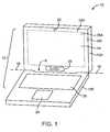
- FIG. 1An illustrative electronic device such as a portable computer or other electronic equipment that has a display is shown in FIG. 1 .
- display 14 of device 10may be mounted in upper housing portion 12A of housing 12.
- Housing 12may be formed from a unibody construction in which some or all of housing 12 is formed form a unitary piece of material (e.g., metal, plastic, or fiber composite materials) or may be formed from multiple structures that have been mounted together using adhesive, fasteners, and other attachment mechanisms.
- housing 12may be formed from frame members and other internal supports to which external plates, housing sidewalls, bezel structures, and other structures are mounted.
- housing portion 12Amay sometimes be referred to as a display housing.
- Display housing 12Amay be attached to housing portion 12B (sometimes referred to as a main unit or base housing) using hinge structures 18, so that display housing 12A may rotate relative to main housing 12B around hinge axis 16.
- Device 10may include ports for removable media, data ports, keys such as keyboard 20, input devices such as track pad 24, microphones, speakers, sensors, status indicators lights, etc.
- Display 14may have an active portion and an inactive portion.
- Active portion 28A of display 14may have a shape such as the rectangular shape that is bounded by dashed line 28D in FIG. 1 .
- Inactive portion 28I of display 14may have a rectangular ring shape or other suitable shape and may form a border around the periphery of display 14.
- Image pixel array elementssuch as liquid crystal diode image pixels or other active image pixel structures may be used in portion 28A to present images to a user of device 10.
- Inactive portion 28Iis generally devoid of image pixel elements and does not participate in forming images for a user.
- an opaque masking layersuch as a layer of ink.
- Device 10may have components that are formed in inactive device region 28I.
- device 10has a camera such as camera 22.
- Camera 22may be mounted within display housing 12A and operates through a window (sometimes referred to as a camera window) in display 14.
- Information structures 26such as a logo may be mounted on device 10.
- Information structures 26may be a trademarked logo that represents a manufacturer of device 10, may be printed text, may be trademarked text, may be a design, may be personalized information (e.g., information identifying an owner of device 10), may be formed from a combination of text and non-text information, or may include other suitable content.
- Information structures 26may be formed from patterned ink, patterned paint, patterned polymer, patterned metal traces, or other suitable materials.
- Information structures 26may be mounted in upper housing 12A.
- information structures 26or may be formed in inactive display region 28I of upper housing 12A under a transparent window in display 14.
- FIG. 2is a perspective view of an illustrative configuration, which may aid understanding of the invention, and that may be used for a handheld electronic device.
- Electronic device 10 of FIG. 2may be, for example, a cellular telephone or other handheld electronic equipment.
- Device 10 of FIG. 1may have housing 12.
- Display 14may be mounted within housing 12 on the front of device 10.
- Active portion 28A of display 14may lie within rectangular boundary 28D.
- Inactive portion 28I of display 14may form a boundary around the periphery of display 14.
- Housing 12may have sidewalls that run around the periphery of device 10 (as an example).
- the sidewall structures of housing 12may be formed from metal, plastic, glass, ceramic, carbon-fiber materials or other fiber-based composites, other materials, or combinations of these materials.
- the rear of housing 12may be formed from metal, plastic, a planar member such as a glass or ceramic plate, fiber-based composites, other materials, or combinations of these materials.
- Openings 34may be used to form microphone and speaker ports, openings to accommodate button members, openings for data ports and audio jacks, etc.
- One or more openingsmay be formed in inactive region 28I of display 14.
- one or more openingsmay be formed in inactive region 28I for buttons such as button 32 (e.g., a menu button).
- Openings such as opening 30may also be formed in inactive region 28I (e.g., to form a speaker port for an ear speaker).
- Window 22is formed over an internal structure in device 10 such as a camera (as an example). If desired, windows such as window 22 may also be formed over information such as logo information (see, e.g., information structures 26 of FIG. 1 ) to allow the logo or other information to be viewed by a user of device 10.
- logo informationsee, e.g., information structures 26 of FIG. 1
- FIGS. 1 and 2are merely examples. Any suitable electronic devices 10 may be provided with displays 14. Electronic devices 10 may, for example, include tablet computers, wristwatch devices, pendant devices, other miniature and wearable devices, televisions, computer displays, accessories, etc.
- FIG. 3A cross-sectional end view of an electronic device with a display (e.g., a device such as device 10 of FIG. 2 , a portion of device 10 of FIG. 1 , etc.) is shown in FIG. 3 .
- display 14may be mounted within housing 12 so that the exterior surface of display 14 is exposed.
- Device housing 12may be used to enclose printed circuit boards such as printed circuit board 36.
- Printed circuit board 36may be a rigid printed circuit board such as a fiberglass-filled epoxy printed circuit board (e.g., FR4), a flexible printed circuit (“flex circuit”) formed from a flexible dielectric such as a sheet of polyimide with patterned conductive traces, a rigid flex substrate, or other substrate.
- Electrical components such as components 37may be mounted to boards such as board 36.
- Electrical components 37may include switches, resistors, inductors, capacitors, integrated circuits, connectors, cameras, sensors, speakers, or other device components. These components may be soldered or otherwise connected to board 36.
- Display 14may be a touch screen display.
- Touch screen displayssuch as display 14 of FIG. 3 may include an array of capacitive electrodes (e.g., transparent electrodes such as indium tin oxide electrodes), or may include a touch sensor array based on other touch technologies (e.g., resistive touch sensor structures, acoustic touch sensor structures, piezoelectric sensors and other force sensor structures, etc.)
- the touch structures for display 14may be implemented on a dedicated touch sensor substrate such as a layer of glass or may be formed on the same layer of glass that is being used for other display functions.
- touch sensor electrodesmay be formed on a color filter array layer, a thin-film transistor layer, or other layers in a liquid crystal display (LCD).
- LCDliquid crystal display
- Display 14may, in general, be formed from any suitable type of display structures including a color filter layer, thin-film transistor and at least one polarizer layer.
- Examples of display structures that may be used for display 14include liquid crystal display (LCD) structures, organic light-emitting diode (OLED) structures, plasma cells, and electronic ink display structures. Arrangements in which display 14 is formed from liquid crystal display (LCD) structures are sometimes described herein as an example. This is merely illustrative. In general, display 14 may be formed using any suitable display technology.
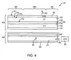
- display 14may include a backlight unit (BLU) such as backlight unit 38.
- BLUbacklight unit
- Light 44 for backlight unit 38may be launched into light-guide panel 51 from light source 32.
- Light source 32may be formed from an array of light-emitting diodes (as an example).
- Reflector 49e.g., white polyester
- Optical films 48may include a diffuser layer and light collimating layers (as an example).
- Display 14 and display module 40may have an active region 28A that produces image pixel light 43 from an array of image pixels.
- Image pixel light 43forms an image in active region 28A that may be viewed by a user of device 10.
- the imagemay include text, graphics, or other image information.
- a portion of display 14 and display module 40 such as region 28Imay be inactive.
- Region 28Imay have a shape that surrounds the periphery of display 14 and display module 40 as shown in FIG. 1 (as an example).
- Inactive region 28Igenerally does not contain active image pixels and may include an opaque masking layer to block interior structures from view.
- Backlight unit 38may have a footprint that is aligned with active region 28A or may have edges that extend under some or all of inactive region 28I (as shown in FIG. 4 ).
- Display module 40includes at least one polarizer such as a lower polarizer 50 and an upper polarizer such as polarizer 62.
- a thin layer (e.g., 3-5 microns) of liquid crystal material 58may be interposed between color filter layer 60 and thin-film transistor layer 52.
- Thin-film transistor layer 52may be formed on a transparent planar substrate such as a layer of glass or plastic.
- the upper surface of thin-film-transistor layer 52may contain pixel electrode structures and thin-film transistors (shown as circuitry 54 above dashed line 56).
- the circuitry on thin-film-transistor layer 52may be organized into an array of image pixels that can be controlled to display images on display 14 for a user of device 10.
- Color filter layer 60includes colored filter pixel elements (e.g., red, green, and blue filter elements) that provide display 14 with the ability to display color images.
- Color filter layer 60is formed using a transparent planar substrate such as a glass or plastic substrate.
- display module 40 and backlight unit 38may include one or more layers of material for forming a touch sensor, layers of optical films such as birefringent compensating films, antireflection coatings, scratch prevention coatings, oleophobic coatings, layers of adhesive, etc.
- layers of optical filmssuch as birefringent compensating films, antireflection coatings, scratch prevention coatings, oleophobic coatings, layers of adhesive, etc.
- Polarizers such as upper (outer) polarizer 62 and lower (inner) polarizer 50may be formed from multiple layers of material that are laminated together.
- An illustrative laminated polarizeris shown in the cross-sectional side view of FIG. 5 .
- polarizer 62i.e., an upper polarizer in this example
- Film 68may be formed from a stretched polymer such as stretched polyvinyl alcohol (PVA) and may therefore sometimes be referred to as a PVA layer.
- Iodinemay be placed on to the stretched PVA film so that iodine molecules align with the stretched film and form the polarizer.
- Other polarizer filmsmay be used if desired.
- Polarizer film 68may be sandwiched between layers 66 and 70.
- Layers 66 and 70may be formed from a material such as tri-acetyl cellulose (TAC) and may sometimes be referred to as TAC films.
- TAC filmsmay help hold the PVA film in its stretched configuration and may protect the PVA film.
- Other filmsmay be laminated to film 68 if desired.
- Coating layer 72may be formed from one or more films of material that provide polarizer 62 with desired surface properties.
- layer 72may be formed from materials that provide polarizer 62 with antiglare (light diffusing) properties, antireflection properties, scratch resistance, fingerprint resistance, and other desired properties.
- Layer 72may be formed from one or more layers of material such as antireflection (AR) layers (e.g., films formed from a stack of alternating high-index-of-refraction and low-index-of-refraction layers), antiglare (AG) layers, antireflection-antiglare (AR/AG) layers, oleophobic layers, antiscratch coatings, or other coating layers.
- ARantireflection
- AGantiglare
- AR/AGantireflection-antiglare
- oleophobic layersoleophobic layers
- antiscratch coatingsor other coating layers.
- an antiglare film in coating 72may help provide polarizer 62 with scratch resistance.
- Polarizer 62may, if desired, be provided with a layer of adhesive such as adhesive 64 (e.g., optically clear adhesive) to help attach polarizer 62 to the upper surface of display module 40 (i.e., color filter 60 of FIG. 4 ).
- adhesive 64e.g., optically clear adhesive
- the thickness of polarizer 62may be about 50-200 microns (as an example).
- a cameramay be mounted under a layer of cover glass in the inactive portion of a display.
- FIG. 6conventional device structures 74 may include cover glass 76.
- Cover glass 76may be associated with a display that has active and inactive regions.
- cover glass 76 of FIG. 6may be associated with inactive display region 98 and active display region 100.
- Black ink layer 78is formed on the underside of cover glass 76 in inactive region 98 and blocks internal components such as camera 86 from view. Black ink layer 78 has opening 80 for camera 86. During operation, light 82 from an image can pass through layer 76 and opening 80 into lens 84 of camera 86.
- Display module 96is mounted under active region 100. Display module 96 includes color filter layer 92, thin-film transistor layer 94, upper polarizer 90, and other LCD layers mounted within chassis structure 88. Black ink 78 hides chassis structure 88 from view.
- the illustrative structures of display 14 of FIG. 4do not include a cover glass layer.
- a camera or other internal device structureis mounted under a portion of the display module.
- FIG. 7shown as a background example, internal structure 102 may be mounted below an edge portion of color filter layer 60 (as an example).
- Internal structure 102may be a camera (e.g., a camera that receives image light through layer 60, a sensor that receives light through layer 60, patterned information structures in the shape of a logo or other information such as structures 26 of FIG. 1 , a status indicator (e.g. a status indicator element that emits light through layer 60), or other suitable internal structures in device 10.
- a camerae.g., a camera that receives image light through layer 60, a sensor that receives light through layer 60, patterned information structures in the shape of a logo or other information such as structures 26 of FIG. 1 , a status indicator (e.g. a status indicator element that emits light through layer 60), or other suitable internal structures in device 10.
- Polarizer 62may interfere with the operation of internal structure 102.
- internal structure 102is a camera
- the presence of polarizer 62 above the camera's image sensormay reduce light intensity and may therefore adversely affect camera performance.
- internal structure 102includes patterned structures that form a logo or other information
- the presence of polarizer 62may make it difficult to view internal structures 102 from the exterior of device 10.
- the operation of light sensors, status indicators, and other electronic componentsmay also be adversely affected by the presence of polarizer layer 62.
- polarizer layer 62One way to minimize any possible adverse impact from polarizer layer 62 involves removing portions of polarizer layer 62, so that color filter layer 60 is exposed. Portions of polarizer layer 62 may be removed following attachment of layer 62 to layer 60 or portions of polarizer layer 62 may be removed prior to attaching layer 62 to layer 60. The portions of layer 62 that are removed have a circular shape (i.e., for forming a circular opening that is aligned with a camera lens), or by way of example only rectangular shapes (e.g., for exposing a logo or other information that has a rectangular outline), or other suitable shapes.
- FIG. 7shows an example not being part of the invention, wherein a polarizer 62 may be removed in region 104 along the edge portion of color filter 60, to avoid overlap between polarizer 62 and internal structures.
- Arrangements of the type shown in FIG. 7may give rise to a step in height at the end of polarizer 62 (i.e., at the interface between polarizer 62 and region 104). In some circumstances, this step may be visible or may allow polarizer 62 to peel away from color filter 60.
- the optical properties in polarizermay be modified to create step-less unpolarized windows that are integral parts of polarizer 62.
- a portion of polarizer 62may be exposed to light with an intensity and wavelength suitable for bleaching (depolarizing) the polarizer material within polarizer layer 62.
- unexposed portions of polarizer 62will function as polarizer layers.
- the exposed portions of polarizer 62will not have significant polarizing properties and will serve as transparent windows.
- Unpolarized windowsmay also be formed in polarizer 62 using other localized treatments (e.g., exposure to a liquid that chemically bleaches polarizer 62, etc.). Using this type of arrangement, polarizer 62 and its unpolarized window regions can smoothly overlap inactive display regions 28I (see, e.g., FIG. 1 ) without introducing steps in height.
- FIGS. 8, 9 and 10An illustrative process for bleaching polarizer 62 by applying light to a localized region of polarizer 62 is shown in FIGS. 8, 9 and 10 .
- polarizer layer 62is formed from a layer of polarizer material with no bleached regions ( FIG. 8 ).
- light source 106may emit light 108 (e.g., ultraviolet light) that strikes a localized region of the surface of polarizer 62.
- Light 108may be localized using a focusing arrangement (e.g., using a lens), using a mask (e.g., using a shadow mask or a patterned masking layer formed on the surface of polarizer 62), using other suitable masking techniques, or using a combination of these techniques.
- the localization of light 108 within polarizer 62causes portion 110 of polarizer 62 to lose its polarizing properties and form a clear window such as window 112.
- polarizer layer 62may be mounted in a device so that internal structure 102 is aligned with window 112.
- the material in window 110e.g., portion 110 of polarizer 62
- window 112may allow light to pass freely between the exterior surface of polarizer layer 62 and internal structure 102.
- the intensity and wavelength of light 108may be selected so as to effectively bleach polarizer 62 without inducing optical damage to polarizer 62 that could adversely affect the transparency and optical clarity of window 112.
- polarizer 62is formed from a stretched PVA layer with a coating of aligned iodine molecules such as layer 68 of FIG. 5
- light 108is preferably able to break iodine bonds or otherwise disorder the PVA polarizer layer without damaging adjacent layers such as TAC layers 66 and 70.
- TAC layers 66 and 70may exhibit satisfactory transmission at wavelengths above about 380 nm or 400 nm.
- FIG. 12shows how PVA absorption (i.e., the absorption in layer 68 of FIG. 5 ) may decrease as a function of increasing wavelength.
- TAC films 66 and 70per FIG. 11
- PVA film 68per FIG. 12
- satisfactory disruption of the polarizer in layer 68 without excessive absorption and resulting damage in TAC layers 66 and 68may be achieved by operating source 106 of FIG. 9 with wavelengths in the range of 380-420 or other wavelengths. Longer wavelengths will be less efficient at bleaching polarizer 62, as indicated by the graph of FIG. 12 , but longer wavelengths will also be less likely to be absorbed in TAC layers 66 and 70 and will therefore tend to be less likely to adversely affect the transparency of TAC layers 66 and 70.
- Ultraviolet light(light with a wavelength of less than 420 nm or less than 400 nm in wavelength) is typically satisfactory for light-bleaching polarizer layer 68, but other types of light may be used if desired.
- the intensity of light 108may be adjusted based on its wavelength. For example, in a scenario in which light 108 has wavelengths in the range of 380-420 nm (as an example), a dose of about 10 J/cm 2 to 100 J/cm 2 (or more or less than 10 J/cm 2 or 100 J/cm 2 ) may be applied to layer 62 to create window 112.
- Unpolarized window 112 in polarizer layer 62may also be formed by chemical treatment.
- polarizer layer 62may initially contain no window regions.
- a masking layersuch as masking layer 114 of FIG. 14 may be applied to the surface of polarizer layer 62.
- Masking layer 114may contain one or more openings such as opening 116.
- Masking layer 114may be pattered using photolithographic techniques (e.g. when masking layer 114 is formed from a photosensitive material such as photoresist), may be patterned by pad printing, spraying, inkjet printing, etc.
- Opening 116may have a size and shape suitable for forming an unpolarized window within polarizer 62.
- a bleaching agentsuch as liquid 118 may be deposited on the surface of layer 62 in opening 116.
- Liquid 118may be, for example, a base such as NaOH, KOH, or other substance that removes the polarization from exposed portions of polarizer layer 62.
- polarizer 62may remain polarized in all areas except unpolarized window 112.
- window 112may be aligned with a camera, information structures such as a logo, or other internal components in device 10, as described in connection with window 112 of FIG. 10 .
- device 10may be provided with one more opaque masks.
- one or more opaque masking layersmay be incorporated onto one or more of the layers of material in display module 40 of FIG. 4 .
- the opaque masking layermay be formed from black ink, ink with other (non-black) colors (e.g., white, silver, gray, red, blue), an opaque polymer, a layer of metal, or other suitable opaque substances.
- locations in which the opaque masking layer may be formed in module 40include position P1 on the top of polarizer 62, position P2 on the lower surface of polarizer 62, position P3 on the top surface of color filter layer 60, and position P4 on the lower surface of color filter layer 60.
- Other masking layer locations and combinations of masking layer locationsmay be used if desired.
- FIG. 17Illustrative steps involved in forming windows in polarizer layer 62 and in forming opaque masking layers and display module structures within an electronic device are shown in FIG. 17 .
- layers of materialsuch as TAC films 66 and 70 and polarizer layer 68 may be laminated together to form polarizer 62.
- an extrusion toolmay be used to stretch PVA layer 68 and laminating rollers may be used to laminating layers 66 and 70 to layer 68.
- Iodinemay be incorporated into the polarizer (e.g., on layer 68).
- window 112may be formed in the laminated polarizer layers during the operations of step 122 (i.e., prior to dividing the TAC and PVA sheets into device-sized panels with a die press or other cutting tool at step 124). Following cutting to form individual panels of polarizer, the polarizer may be laminated to color filter layer 60 (step 126).
- the layers of polarizer that have been laminated together during the operations of step 120may be divided into individual panels during the operations of step 130 (i.e., before forming window 112 in polarizer 62 during the operations of step 132).
- the panel of polarizer in which window 112 is formed during step 132may be laminated to color filter layer 60 at step 126.
- polarizer that has been cut into device-sized panels during the operations of step 130may be laminated to color filter layer 60 (step 134) before forming window 112 (step 136).
- polarizer 62 and other display structuresmay, during the operation of step 128 be assembled into device 10 so that a camera or other internal structures (see, e.g., structure 102 of FIG. 10 ) are mounted in alignment with window 112.
- opaque masking layersmay be formed on the layers of material that form display 14. For example, a patterned layer of ink or other opaque masking material may be formed in locations such as locations P1, P2, P3, and P4 in display module 40 (see, e.g., FIG. 4 ).
- Patterned masking layersmay be formed using physical vapor deposition, pad printing, screen printing, spraying, dipping, inkjet printing, shadow mask deposition, photolithographic patterning, or other suitable deposition and patterning techniques.
- materials that may be used as opaque masking layersinclude metals, polymers, ink, paint, tinted adhesive, oxides (e.g., metal oxides), fiber-based composites, etc.
- FIG. 18is a cross-sectional side view of display structures not part of the invention in which an opaque masking layer has been formed in a position such as position P4 of FIG. 4 under color filter layer 60.
- display module 40may have active region 28A and inactive region 28I.
- Opaque masking layer 138may be formed on the inner surface of color filter layer 60.
- Opaque masking layer 138may be patterned to form an opening such as opening 140.
- Opening 140may have a size and shape that allows some or all of opening 140 to overlap window 112 in polarizer layer 62. This allows light to pass between interior structure 102 and the exterior of module 40 adjacent to polarizer 62 via window 112, color filter 60, opening 140, and thin-film transistor layer 52 (as an example).
- masking layer 138may overlap existing structures on color filter 60 (e.g., structures such as structure 142 of FIG. 18 that are formed of chromium or other materials and that are used in forming light-blocking patterns for the color filter elements in filter 60). If desired, some of structures 142 may be used in forming layers such as layer 138.
- internal structures 102may be aligned along common vertical axis 114 with window 112 and mask opening 140.
- Structures 102may include a camera (image sensor), a status indicator, information structures such as a logo or other printed or patterned information, a sensor, etc.
- FIGS. 19A, 19B, and 19Cshow how internal structures 102 such as information structures that form a logo or other information may be formed on the lower surface of color filter layer 60 in a configuration in which masking layer 138 is being formed in a position such as position P4 of FIG. 4 .
- structures 102may be formed on the lower surface of color filter 60.
- Structures 102may, for example, be formed under window 112 in polarizer layer 62 (i.e., so that the outline of structures 102 is contained within the outline of window 112 and so that window 112 completely overlaps structures 102).
- Structures 102may be formed from ink, metal, paint, polymer, or other materials and may be deposited using physical vapor deposition (PVD) or other suitable deposition and patterning techniques.
- PVDphysical vapor deposition
- opaque masking layer 138may be formed over structures 102, as shown in FIG. 19B .
- a layer of black ink or other opaque masking substancemay be formed over structures 102 (e.g., a PVD logo) using screen printing, inkjet printing, pad printing, or other suitable deposition techniques.
- Opaque masking layer 138may cover the inactive portion of display 14 (see, e.g., inactive portion 28I of FIG. 1 ).
- display module 40may be completed by attaching lower polarizer 50 and thin-film-transistor layer 52 below liquid crystal material 58, color filter layer 60, and upper polarizer 62.
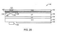
- FIG. 20is a cross-sectional side view of display module 40 in a configuration in which opaque masking layer 138 has been formed in a position such as position P3 of FIG. 4 (i.e., on top of color filter layer 60).
- polarizer 62may be provided with unpolarized window 112 that is aligned with internal structures 102 (e.g., a logo or other information, a camera, a sensor or other electrical component, etc.).
- Opaque masking layer 138may have an opening such as opening 140 that is aligned with window 112 and structures 102.
- Polarizer layer 62may be attached to display module 40 using adhesive 148 (e.g., a layer of adhesive that is about 0.5 to 6 microns thick).
- Opaque masking layer 138may be about 40 to 120 microns thick (as an example). If desired, planarizing layer 146 may be interposed between polarizer 62 and the upper surface of color filter layer 60 to help accommodate the thickness of opaque masking layer 138. Planarizing layer 146 may be formed from epoxy or other adhesive (e.g., some of adhesive 148), spin-on-glass, polymer, or other clear material. Opaque masking layer 138 may be formed from white ink, black ink, non-black colored ink, or other suitable opaque materials.
- color filter layer 60may, if desired, be provided with a recess such as recess 150.
- Recess 150may have a depth (thickness) comparable to the thickness of opaque masking layer 138 (e.g., about 40-120 microns as an example).
- opaque masking layerand, if desired, optional filler material 152) may be recessed within recess 150 so that the outermost surface of opaque masking layer 138 (and optional filler material 152) is flush or nearly flush with the outermost surface of color filter layer 160.
- Filler material 152may be formed from adhesive (e.g., some of adhesive 148), polymer, or other suitable transparent materials.
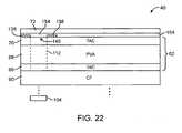
- FIG. 22A cross-sectional side view of an illustrative configuration that may be used for display module 40 in which opaque masking layer 138 is formed on polarizer 62 (e.g., in position P1 of FIG. 4 ) is shown in FIG. 22 .
- polarizer 62may include a polarizer layer such as PVA layer 68 and TAC layers such as TAC layers 66 and 70 or other optical films.
- Polarizer 62may be attached to color filter layer 60 (e.g., using adhesive).
- Opaque masking layer 138may be formed on the surface of TAC layer 70. Opening 140 may be aligned with window 112 in polarizer 62.
- Cover film 72may be attached to the outer surface of TAC layer 70 (e.g., to form the outermost surface of display module 40).
- Cover film 72may be a cover layer that includes one or more layers such as antireflection layers, antiglare layers, antiscratch layers, etc.
- Cover film 72may be dispensed from one or more rolls of film and may be attached to TAC layer 70 using adhesive 154.
- opaque masking layer 138may be aligned with the panel of material that forms polarizer 62 to a relatively high tolerance (e.g., to a 0.1-0.4 mm tolerance), because layer 138 can be aligned directly to the polarizer panel during printing operations or other opaque masking layer deposition operations (as an example). If desired, opaque masking layer 138 may be deposited onto the underside of cover film 72 before cover film 72 is attached to polarizer 62.
- FIG. 23is a cross-sectional side view of illustrative structures for display module 40 showing how opaque masking layer 138 may be formed on the underside of polarizer 62 in alignment with window 112.
- Adhesive 64may be used to attach polarizer 62 to color filter layer 60 when polarizer 62 is moved in direction 156.
- a recessmay be provided in color filter layer 60 to help accommodate the thickness of opaque masking layer 138, a layer of planarizing material may be interposed between polarizer 62 and color filter 60, or other actions may be taken to help ensure that polarizer 62 is satisfactorily attached to color filter 60.
Landscapes
- Engineering & Computer Science (AREA)
- Physics & Mathematics (AREA)
- Theoretical Computer Science (AREA)
- Computer Hardware Design (AREA)
- General Physics & Mathematics (AREA)
- General Engineering & Computer Science (AREA)
- Human Computer Interaction (AREA)
- Nonlinear Science (AREA)
- Mathematical Physics (AREA)
- Signal Processing (AREA)
- Multimedia (AREA)
- Optics & Photonics (AREA)
- Chemical & Material Sciences (AREA)
- Crystallography & Structural Chemistry (AREA)
- Polarising Elements (AREA)
- Liquid Crystal (AREA)
- Devices For Indicating Variable Information By Combining Individual Elements (AREA)
- Optical Filters (AREA)
Description
- This invention relates to electronic devices and, more particularly, to display structures for electronic devices such as portable computers.
- Electronic devices such as portable computers and cellular telephones typically have displays. To provide protection from damage, many displays are provided with cover glass layers. The cover glass layer helps protect underlying display structures from scratches and other damage during use of the electronic device. A patterned layer of black ink is sometimes formed on the underside of the cover glass layer to form an opaque border region. The opaque border region can hide internal device components from view. An opening in the black ink can be provided for a camera that is mounted behind the cover glass.
- As device manufacturers strive to reduce device size and weight, it is becoming unacceptable to include potentially bulky and heavy display structures in a display. It may therefore be desirable to omit the cover glass layer from a display. Care must be taken, however, to ensure that unsightly internal components remain hidden from view and that internal components such as cameras are still able to function properly.
- It would therefore be desirable to be able to provide improved display structures in electronic devices such as portable computers and cellular telephones.
US 2004/0212555 A1 discloses a portable electronic device with an integral display and a camera. The device includes a printed circuit board, a display having one or more display layers, and an integrated camera coupled between the one or more display layers and the printed circuit board, wherein the one or more display layers are constructed such that a light stream flows through to the integrated camera.US 2010/0039530 A1 discloses an apparatus and method for compensating for variations in digital cameras.US 2010/0020277 A1 discloses a liquid crystal display device.- There is provided a portable computer as defined in the attached claims. Other features will be apparent from the description which follows.
- An electronic device such as a portable computer, cellular telephone, or other electronic equipment has a display. The display may have an active portion such as a central rectangular region in which images are presented to a user of the device. Inactive portions of the display such as peripheral portions of the display may be masked using an opaque masking layer. The opaque masking layer may be formed from colored ink.
- An opening may be provided in the opaque masking layer to allow light to pass. For example, a logo or other information may be viewed through an opening in the opaque masking layer. Cameras and other internal electronic components may receive light through an opening in the opaque masking layer.
- The display includes at least one polarizer, a color filter layer, and a thin-film transistor layer. The opaque masking layer may be formed on the at least one polarizer, may be interposed between the at least one polarizer and the color filter layer, or may be interposed between the color filter layer and the thin-film transistor layer.
- Further features of the invention, its nature and various advantages will be more apparent from the accompanying drawings and the following detailed description of the preferred embodiments.
FIG. 1 is a perspective view of an illustrative portable computer with display structures in accordance with an embodiment of the present invention.FIG. 2 is a perspective view of a handheld device.FIG. 3 is a cross-sectional side view of an electronic device having a display.FIG. 4 is a cross-sectional side view of illustrative display structures.FIG. 5 is a cross-sectional side view of a polarizer for an electronic device display.FIG. 6 is a cross-sectional side view of a conventional liquid crystal display (LCD) module in a portable computer.FIG. 7 is a cross-sectional side view of an illustrative display having a recessed polarizer layer that exposes internal device structures.FIG. 8 is a cross-sectional side view of a polarizer layer prior to treatment to form a transparent unpolarized window.FIG. 9 is a cross-sectional side view of the polarizer ofFIG. 8 during exposure of a portion of the polarizer to ultraviolet light to bleach the polarizer and thereby form a window in the polarizer.FIG. 10 is a cross-sectional side view of a polarizer having a transparent unpolarized (bleached) window with which an internal device structure has been aligned.FIG. 11 is a graph showing how transmission for a film such as a triacetate cellulose (TAC) film within a laminated polarizer may vary as a function of wavelength.FIG. 12 is a graph showing how absorption for a film such as a polyvinyl alcohol film in a laminated polarizer may vary as a function of wavelength.FIG. 13 is a cross-sectional side view of a polarizer prior to formation of a patterned masking layer on the surface of the polarizer.FIG. 14 is a cross-sectional side view of the polarizer layer ofFIG. 14 following formation of a patterned masking layer.FIG. 15 is a cross-sectional side view of the masked polarizer layer ofFIG. 14 showing how a liquid depolarizing agent may be applied on top of the patterned masking layer to form an unpolarized region within the polarizer layer.FIG. 16 is a cross-sectional side view of the polarizer layer ofFIG. 15 following removal of the masking layer to complete formation of a chemically bleached unpolarized window in the polarizer layer.FIG. 17 is a flow chart of illustrative steps involved in forming display structures including a polarizer layer with an unpolarized window and an opaque masking layer with an opening.FIG. 18 is a cross-sectional side view of illustrative display structures having a polarizer with an unpolarized window and a patterned opaque masking layer formed on the inner surface of a color filter layer.FIG. 19A is a cross-sectional side view of illustrative display structures having a polarizer with an unpolarized window that is aligned with a logo or other information printed on the inner surface of a color filter layer using physical vapor deposition (PVD).FIG. 19B is a cross-sectional side view of the display structures ofFIG. 19A following formation of an opaque masking layer over the logo.FIG. 19C is a cross-sectional side view of the display structures ofFIG. 19B after the color filter and polarizer layers have been connected to other display structure layers such as a thin-film-transistor layer.FIG. 20 is a cross-sectional side view of illustrative display structures having a polarizer with an unpolarized window and a patterned opaque masking layer formed on the outer surface of a color filter layer.FIG. 21 is a cross-sectional side view of illustrative display structures having a polarizer with an unpolarized window and a patterned opaque masking layer formed within a recessed region on the outer surface of a color filter layer.FIG. 22 is a cross-sectional side view of illustrative display structures having a polarizer with an unpolarized window and a patterned opaque masking layer that is formed on a layer of the polarizer such as a triacetate cellulose layer and that is interposed between the outer surface of the triacetate cellulose layer and an inner surface of a cover film.FIG. 23 is a cross-sectional side view of illustrative display structures having a polarizer with an unpolarized window and a patterned opaque masking layer formed on the inner surface of a polarizer layer.- Electronic devices such as notebook computers, tablet computers, cellular telephones, and other computing equipment may be provided with displays.
- An illustrative electronic device such as a portable computer or other electronic equipment that has a display is shown in
FIG. 1 . As shown inFIG. 1 ,display 14 ofdevice 10 may be mounted inupper housing portion 12A ofhousing 12.Housing 12 may be formed from a unibody construction in which some or all ofhousing 12 is formed form a unitary piece of material (e.g., metal, plastic, or fiber composite materials) or may be formed from multiple structures that have been mounted together using adhesive, fasteners, and other attachment mechanisms. For example,housing 12 may be formed from frame members and other internal supports to which external plates, housing sidewalls, bezel structures, and other structures are mounted. - Because
housing portion 12A is used to housedisplay 14,housing portion 12A may sometimes be referred to as a display housing.Display housing 12A may be attached tohousing portion 12B (sometimes referred to as a main unit or base housing) usinghinge structures 18, so thatdisplay housing 12A may rotate relative tomain housing 12B aroundhinge axis 16.Device 10 may include ports for removable media, data ports, keys such askeyboard 20, input devices such astrack pad 24, microphones, speakers, sensors, status indicators lights, etc. Display 14 may have an active portion and an inactive portion.Active portion 28A ofdisplay 14 may have a shape such as the rectangular shape that is bounded by dashedline 28D inFIG. 1 . Inactive portion 28I ofdisplay 14 may have a rectangular ring shape or other suitable shape and may form a border around the periphery ofdisplay 14. Image pixel array elements such as liquid crystal diode image pixels or other active image pixel structures may be used inportion 28A to present images to a user ofdevice 10. Inactive portion 28I is generally devoid of image pixel elements and does not participate in forming images for a user. To hide unsightly internal components from view, internal components ininactive portion 281 may be blocked from view using an opaque masking layer such as a layer of ink.Device 10 may have components that are formed in inactive device region 28I. For example,device 10 has a camera such ascamera 22.Camera 22 may be mounted withindisplay housing 12A and operates through a window (sometimes referred to as a camera window) indisplay 14.Information structures 26 such as a logo may be mounted ondevice 10.Information structures 26 may be a trademarked logo that represents a manufacturer ofdevice 10, may be printed text, may be trademarked text, may be a design, may be personalized information (e.g., information identifying an owner of device 10), may be formed from a combination of text and non-text information, or may include other suitable content.Information structures 26 may be formed from patterned ink, patterned paint, patterned polymer, patterned metal traces, or other suitable materials.Information structures 26 may be mounted inupper housing 12A. For example,information structures 26 or may be formed in inactive display region 28I ofupper housing 12A under a transparent window indisplay 14.FIG. 2 is a perspective view of an illustrative configuration, which may aid understanding of the invention, and that may be used for a handheld electronic device.Electronic device 10 ofFIG. 2 may be, for example, a cellular telephone or other handheld electronic equipment.Device 10 ofFIG. 1 may havehousing 12.Display 14 may be mounted withinhousing 12 on the front ofdevice 10.Active portion 28A ofdisplay 14 may lie withinrectangular boundary 28D. Inactive portion 28I ofdisplay 14 may form a boundary around the periphery ofdisplay 14.Housing 12 may have sidewalls that run around the periphery of device 10 (as an example). The sidewall structures ofhousing 12 may be formed from metal, plastic, glass, ceramic, carbon-fiber materials or other fiber-based composites, other materials, or combinations of these materials. The rear ofhousing 12 may be formed from metal, plastic, a planar member such as a glass or ceramic plate, fiber-based composites, other materials, or combinations of these materials.Device 10 may have openings such asopenings 34 in the sidewalls ofhousing 12.Openings 34 may be used to form microphone and speaker ports, openings to accommodate button members, openings for data ports and audio jacks, etc. One or more openings may be formed in inactive region 28I ofdisplay 14. For example, one or more openings may be formed in inactive region 28I for buttons such as button 32 (e.g., a menu button). Openings such asopening 30 may also be formed in inactive region 28I (e.g., to form a speaker port for an ear speaker).Window 22 is formed over an internal structure indevice 10 such as a camera (as an example). If desired, windows such aswindow 22 may also be formed over information such as logo information (see, e.g.,information structures 26 ofFIG. 1 ) to allow the logo or other information to be viewed by a user ofdevice 10.- The illustrative electronic device structures of
FIGS. 1 and2 are merely examples. Any suitableelectronic devices 10 may be provided withdisplays 14.Electronic devices 10 may, for example, include tablet computers, wristwatch devices, pendant devices, other miniature and wearable devices, televisions, computer displays, accessories, etc. - A cross-sectional end view of an electronic device with a display (e.g., a device such as
device 10 ofFIG. 2 , a portion ofdevice 10 ofFIG. 1 , etc.) is shown inFIG. 3 . As shown inFIG. 3 ,display 14 may be mounted withinhousing 12 so that the exterior surface ofdisplay 14 is exposed.Device housing 12 may be used to enclose printed circuit boards such as printedcircuit board 36. Printedcircuit board 36 may be a rigid printed circuit board such as a fiberglass-filled epoxy printed circuit board (e.g., FR4), a flexible printed circuit ("flex circuit") formed from a flexible dielectric such as a sheet of polyimide with patterned conductive traces, a rigid flex substrate, or other substrate. - Electrical components such as
components 37 may be mounted to boards such asboard 36.Electrical components 37 may include switches, resistors, inductors, capacitors, integrated circuits, connectors, cameras, sensors, speakers, or other device components. These components may be soldered or otherwise connected to board 36. Display 14 may be a touch screen display. Touch screen displays such asdisplay 14 ofFIG. 3 may include an array of capacitive electrodes (e.g., transparent electrodes such as indium tin oxide electrodes), or may include a touch sensor array based on other touch technologies (e.g., resistive touch sensor structures, acoustic touch sensor structures, piezoelectric sensors and other force sensor structures, etc.) The touch structures fordisplay 14 may be implemented on a dedicated touch sensor substrate such as a layer of glass or may be formed on the same layer of glass that is being used for other display functions. For example, touch sensor electrodes may be formed on a color filter array layer, a thin-film transistor layer, or other layers in a liquid crystal display (LCD).Display 14 may, in general, be formed from any suitable type of display structures including a color filter layer, thin-film transistor and at least one polarizer layer. Examples of display structures that may be used fordisplay 14 include liquid crystal display (LCD) structures, organic light-emitting diode (OLED) structures, plasma cells, and electronic ink display structures. Arrangements in which display 14 is formed from liquid crystal display (LCD) structures are sometimes described herein as an example. This is merely illustrative. In general,display 14 may be formed using any suitable display technology.- A cross-sectional view of
display 14 ofFIG. 2 is shown inFIG. 4 . As shown inFIG. 4 ,display 14 may include a backlight unit (BLU) such asbacklight unit 38.Light 44 forbacklight unit 38 may be launched into light-guide panel 51 fromlight source 32.Light source 32 may be formed from an array of light-emitting diodes (as an example). Reflector 49 (e.g., white polyester) may be used to reflect light 44 upwards (outwards) indirection 46 throughdisplay module 40.Optical films 48 may include a diffuser layer and light collimating layers (as an example). Display 14 anddisplay module 40 may have anactive region 28A that produces image pixel light 43 from an array of image pixels. Image pixel light 43 forms an image inactive region 28A that may be viewed by a user ofdevice 10. The image may include text, graphics, or other image information. A portion ofdisplay 14 anddisplay module 40 such as region 28I may be inactive. Region 28I may have a shape that surrounds the periphery ofdisplay 14 anddisplay module 40 as shown inFIG. 1 (as an example). Inactive region 28I generally does not contain active image pixels and may include an opaque masking layer to block interior structures from view.Backlight unit 38 may have a footprint that is aligned withactive region 28A or may have edges that extend under some or all of inactive region 28I (as shown inFIG. 4 ).Display module 40 includes at least one polarizer such as alower polarizer 50 and an upper polarizer such aspolarizer 62. A thin layer (e.g., 3-5 microns) ofliquid crystal material 58 may be interposed betweencolor filter layer 60 and thin-film transistor layer 52.- Thin-
film transistor layer 52 may be formed on a transparent planar substrate such as a layer of glass or plastic. The upper surface of thin-film-transistor layer 52 may contain pixel electrode structures and thin-film transistors (shown ascircuitry 54 above dashed line 56). The circuitry on thin-film-transistor layer 52 may be organized into an array of image pixels that can be controlled to display images ondisplay 14 for a user ofdevice 10. Color filter layer 60 includes colored filter pixel elements (e.g., red, green, and blue filter elements) that providedisplay 14 with the ability to display color images.Color filter layer 60 is formed using a transparent planar substrate such as a glass or plastic substrate.- If desired, other layers of material may be included within
display module 40 andbacklight unit 38. For example,display module 40 andbacklight unit 38 may include one or more layers of material for forming a touch sensor, layers of optical films such as birefringent compensating films, antireflection coatings, scratch prevention coatings, oleophobic coatings, layers of adhesive, etc. - Polarizers such as upper (outer) polarizer 62 and lower (inner)
polarizer 50 may be formed from multiple layers of material that are laminated together. An illustrative laminated polarizer is shown in the cross-sectional side view ofFIG. 5 . As shown inFIG. 5 , polarizer 62 (i.e., an upper polarizer in this example) may havepolarizer film 68.Film 68 may be formed from a stretched polymer such as stretched polyvinyl alcohol (PVA) and may therefore sometimes be referred to as a PVA layer. Iodine may be placed on to the stretched PVA film so that iodine molecules align with the stretched film and form the polarizer. Other polarizer films may be used if desired.Polarizer film 68 may be sandwiched betweenlayers Layers Coating layer 72 may be formed from one or more films of material that providepolarizer 62 with desired surface properties. For example,layer 72 may be formed from materials that providepolarizer 62 with antiglare (light diffusing) properties, antireflection properties, scratch resistance, fingerprint resistance, and other desired properties.Layer 72 may be formed from one or more layers of material such as antireflection (AR) layers (e.g., films formed from a stack of alternating high-index-of-refraction and low-index-of-refraction layers), antiglare (AG) layers, antireflection-antiglare (AR/AG) layers, oleophobic layers, antiscratch coatings, or other coating layers. The functions of these layers need not be mutually exclusive. For example, an antiglare film incoating 72 may help provide polarizer 62 with scratch resistance.Polarizer 62 may, if desired, be provided with a layer of adhesive such as adhesive 64 (e.g., optically clear adhesive) to help attachpolarizer 62 to the upper surface of display module 40 (i.e.,color filter 60 ofFIG. 4 ). The thickness ofpolarizer 62 may be about 50-200 microns (as an example).- It is often desirable to mount cameras within the interior of an electronic device. Conventionally, a camera may be mounted under a layer of cover glass in the inactive portion of a display. This type of arrangement is shown in
FIG. 6 . As shown inFIG. 6 ,conventional device structures 74 may includecover glass 76.Cover glass 76 may be associated with a display that has active and inactive regions. For example,cover glass 76 ofFIG. 6 may be associated withinactive display region 98 andactive display region 100. Black ink layer 78 is formed on the underside ofcover glass 76 ininactive region 98 and blocks internal components such ascamera 86 from view.Black ink layer 78 hasopening 80 forcamera 86. During operation, light 82 from an image can pass throughlayer 76 andopening 80 intolens 84 ofcamera 86.Display module 96 is mounted underactive region 100.Display module 96 includescolor filter layer 92, thin-film transistor layer 94,upper polarizer 90, and other LCD layers mounted withinchassis structure 88.Black ink 78hides chassis structure 88 from view.- The illustrative structures of
display 14 ofFIG. 4 do not include a cover glass layer. In this type of arrangement, it may be desirable to mount cameras and other internal structures under a portion of a housing that is separate from display 14 (e.g., under a camera opening in a bezel or other housing structure). If desired, a camera or other internal device structure is mounted under a portion of the display module. As shown inFIG. 7 , shown as a background example,internal structure 102 may be mounted below an edge portion of color filter layer 60 (as an example).Internal structure 102 may be a camera (e.g., a camera that receives image light throughlayer 60, a sensor that receives light throughlayer 60, patterned information structures in the shape of a logo or other information such asstructures 26 ofFIG. 1 , a status indicator (e.g. a status indicator element that emits light through layer 60), or other suitable internal structures indevice 10. Polarizer 62 may interfere with the operation ofinternal structure 102. For example, ifinternal structure 102 is a camera, the presence ofpolarizer 62 above the camera's image sensor may reduce light intensity and may therefore adversely affect camera performance. As another example, ifinternal structure 102 includes patterned structures that form a logo or other information, the presence ofpolarizer 62 may make it difficult to viewinternal structures 102 from the exterior ofdevice 10. The operation of light sensors, status indicators, and other electronic components may also be adversely affected by the presence ofpolarizer layer 62.- One way to minimize any possible adverse impact from
polarizer layer 62 involves removing portions ofpolarizer layer 62, so thatcolor filter layer 60 is exposed. Portions ofpolarizer layer 62 may be removed following attachment oflayer 62 to layer 60 or portions ofpolarizer layer 62 may be removed prior to attachinglayer 62 to layer 60. The portions oflayer 62 that are removed have a circular shape (i.e., for forming a circular opening that is aligned with a camera lens), or by way of example only rectangular shapes (e.g., for exposing a logo or other information that has a rectangular outline), or other suitable shapes.FIG. 7 shows an example not being part of the invention, wherein apolarizer 62 may be removed inregion 104 along the edge portion ofcolor filter 60, to avoid overlap betweenpolarizer 62 and internal structures. - Arrangements of the type shown in
FIG. 7 may give rise to a step in height at the end of polarizer 62 (i.e., at the interface betweenpolarizer 62 and region 104). In some circumstances, this step may be visible or may allowpolarizer 62 to peel away fromcolor filter 60. - As a non-claimed example, to avoid creating a step in height, the optical properties in polarizer may be modified to create step-less unpolarized windows that are integral parts of
polarizer 62. For example, a portion ofpolarizer 62 may be exposed to light with an intensity and wavelength suitable for bleaching (depolarizing) the polarizer material withinpolarizer layer 62. Following light exposure, unexposed portions ofpolarizer 62 will function as polarizer layers. The exposed portions ofpolarizer 62 will not have significant polarizing properties and will serve as transparent windows. Unpolarized windows may also be formed inpolarizer 62 using other localized treatments (e.g., exposure to a liquid that chemically bleachespolarizer 62, etc.). Using this type of arrangement,polarizer 62 and its unpolarized window regions can smoothly overlap inactive display regions 28I (see, e.g.,FIG. 1 ) without introducing steps in height. - An illustrative process for bleaching
polarizer 62 by applying light to a localized region ofpolarizer 62 is shown inFIGS. 8, 9 and 10 . Initially,polarizer layer 62 is formed from a layer of polarizer material with no bleached regions (FIG. 8 ). As shown inFIG. 9 ,light source 106 may emit light 108 (e.g., ultraviolet light) that strikes a localized region of the surface ofpolarizer 62.Light 108 may be localized using a focusing arrangement (e.g., using a lens), using a mask (e.g., using a shadow mask or a patterned masking layer formed on the surface of polarizer 62), using other suitable masking techniques, or using a combination of these techniques. The localization oflight 108 withinpolarizer 62 causesportion 110 ofpolarizer 62 to lose its polarizing properties and form a clear window such aswindow 112. - As shown in
FIG. 10 ,polarizer layer 62 may be mounted in a device so thatinternal structure 102 is aligned withwindow 112. The material in window 110 (e.g.,portion 110 of polarizer 62) is not polarized, sowindow 112 may allow light to pass freely between the exterior surface ofpolarizer layer 62 andinternal structure 102. - The intensity and wavelength of
light 108 may be selected so as to effectivelybleach polarizer 62 without inducing optical damage to polarizer 62 that could adversely affect the transparency and optical clarity ofwindow 112. If, for example,polarizer 62 is formed from a stretched PVA layer with a coating of aligned iodine molecules such aslayer 68 ofFIG. 5 , light 108 is preferably able to break iodine bonds or otherwise disorder the PVA polarizer layer without damaging adjacent layers such as TAC layers 66 and 70. As shown inFIG. 11 , TAC layers 66 and 70 may exhibit satisfactory transmission at wavelengths above about 380 nm or 400 nm.FIG. 12 shows how PVA absorption (i.e., the absorption inlayer 68 ofFIG. 5 ) may decrease as a function of increasing wavelength. - Taking into consideration the properties of
TAC films 66 and 70 (perFIG. 11 ) and the properties of PVA film 68 (perFIG. 12 ), satisfactory disruption of the polarizer inlayer 68 without excessive absorption and resulting damage in TAC layers 66 and 68 may be achieved by operatingsource 106 ofFIG. 9 with wavelengths in the range of 380-420 or other wavelengths. Longer wavelengths will be less efficient atbleaching polarizer 62, as indicated by the graph ofFIG. 12 , but longer wavelengths will also be less likely to be absorbed in TAC layers 66 and 70 and will therefore tend to be less likely to adversely affect the transparency of TAC layers 66 and 70. Ultraviolet light (light with a wavelength of less than 420 nm or less than 400 nm in wavelength) is typically satisfactory for light-bleaching polarizer layer 68, but other types of light may be used if desired. - The intensity of
light 108 may be adjusted based on its wavelength. For example, in a scenario in which light 108 has wavelengths in the range of 380-420 nm (as an example), a dose of about 10 J/cm2 to 100 J/cm2 (or more or less than 10 J/cm2 or 100 J/cm2) may be applied tolayer 62 to createwindow 112. Unpolarized window 112 inpolarizer layer 62 may also be formed by chemical treatment. Consider, as an example, the application of bleaching liquid topolarizer layer 62, as illustrated inFIGS. 13-16 . As shown inFIG. 13 ,polarizer layer 62 may initially contain no window regions. A masking layer such asmasking layer 114 ofFIG. 14 may be applied to the surface ofpolarizer layer 62. Maskinglayer 114 may contain one or more openings such asopening 116. Maskinglayer 114 may be pattered using photolithographic techniques (e.g. when maskinglayer 114 is formed from a photosensitive material such as photoresist), may be patterned by pad printing, spraying, inkjet printing, etc. Opening 116 may have a size and shape suitable for forming an unpolarized window withinpolarizer 62. As shown inFIG. 15 , afterlayer 114 has been formed, a bleaching agent such asliquid 118 may be deposited on the surface oflayer 62 inopening 116.Liquid 118 may be, for example, a base such as NaOH, KOH, or other substance that removes the polarization from exposed portions ofpolarizer layer 62.- As shown in
FIG. 16 , following application and removal ofmasking layer 114 and liquid 118 (or other suitable bleaching agent),polarizer 62 may remain polarized in all areas exceptunpolarized window 112. - During assembly of
polarizer 62 intodevice 10,window 112 may be aligned with a camera, information structures such as a logo, or other internal components indevice 10, as described in connection withwindow 112 ofFIG. 10 . To ensure that potentially unsightly internal portions ofdevice 10 are blocked from view,device 10 may be provided with one more opaque masks. For example, one or more opaque masking layers may be incorporated onto one or more of the layers of material indisplay module 40 ofFIG. 4 . The opaque masking layer may be formed from black ink, ink with other (non-black) colors (e.g., white, silver, gray, red, blue), an opaque polymer, a layer of metal, or other suitable opaque substances. Examples of locations in which the opaque masking layer may be formed inmodule 40 include position P1 on the top ofpolarizer 62, position P2 on the lower surface ofpolarizer 62, position P3 on the top surface ofcolor filter layer 60, and position P4 on the lower surface ofcolor filter layer 60. Other masking layer locations and combinations of masking layer locations may be used if desired. - Illustrative steps involved in forming windows in
polarizer layer 62 and in forming opaque masking layers and display module structures within an electronic device are shown inFIG. 17 . - At
step 120, layers of material such asTAC films polarizer layer 68 may be laminated together to formpolarizer 62. For example, an extrusion tool may be used to stretchPVA layer 68 and laminating rollers may be used tolaminating layers layer 68. Iodine may be incorporated into the polarizer (e.g., on layer 68). - If desired,
window 112 may be formed in the laminated polarizer layers during the operations of step 122 (i.e., prior to dividing the TAC and PVA sheets into device-sized panels with a die press or other cutting tool at step 124). Following cutting to form individual panels of polarizer, the polarizer may be laminated to color filter layer 60 (step 126). - Alternatively, the layers of polarizer that have been laminated together during the operations of
step 120 may be divided into individual panels during the operations of step 130 (i.e., before formingwindow 112 inpolarizer 62 during the operations of step 132). With this type of approach, the panel of polarizer in whichwindow 112 is formed duringstep 132 may be laminated tocolor filter layer 60 atstep 126. - If desired, polarizer that has been cut into device-sized panels during the operations of
step 130 may be laminated to color filter layer 60 (step 134) before forming window 112 (step 136). - Regardless of the order in which polarizer 62 is processed to form
window 112 and attached tocolor filter layer 60,polarizer 62 and other display structures may, during the operation ofstep 128 be assembled intodevice 10 so that a camera or other internal structures (see, e.g.,structure 102 ofFIG. 10 ) are mounted in alignment withwindow 112. Prior to the assembly operations ofstep 128 or during assembly, opaque masking layers may be formed on the layers of material that formdisplay 14. For example, a patterned layer of ink or other opaque masking material may be formed in locations such as locations P1, P2, P3, and P4 in display module 40 (see, e.g.,FIG. 4 ). Patterned masking layers may be formed using physical vapor deposition, pad printing, screen printing, spraying, dipping, inkjet printing, shadow mask deposition, photolithographic patterning, or other suitable deposition and patterning techniques. Examples of materials that may be used as opaque masking layers include metals, polymers, ink, paint, tinted adhesive, oxides (e.g., metal oxides), fiber-based composites, etc. FIG. 18 is a cross-sectional side view of display structures not part of the invention in which an opaque masking layer has been formed in a position such as position P4 ofFIG. 4 undercolor filter layer 60. As shown inFIG. 18 ,display module 40 may haveactive region 28A and inactive region 28I.Opaque masking layer 138 may be formed on the inner surface ofcolor filter layer 60.Opaque masking layer 138 may be patterned to form an opening such asopening 140. Opening 140 may have a size and shape that allows some or all ofopening 140 to overlapwindow 112 inpolarizer layer 62. This allows light to pass betweeninterior structure 102 and the exterior ofmodule 40 adjacent to polarizer 62 viawindow 112,color filter 60, opening 140, and thin-film transistor layer 52 (as an example). During deposition operations, some or all ofmasking layer 138 may overlap existing structures on color filter 60 (e.g., structures such asstructure 142 ofFIG. 18 that are formed of chromium or other materials and that are used in forming light-blocking patterns for the color filter elements in filter 60). If desired, some ofstructures 142 may be used in forming layers such aslayer 138.- As shown in
FIG. 18 ,internal structures 102 may be aligned along commonvertical axis 114 withwindow 112 andmask opening 140.Structures 102 may include a camera (image sensor), a status indicator, information structures such as a logo or other printed or patterned information, a sensor, etc. FIGS. 19A, 19B, and 19C show howinternal structures 102 such as information structures that form a logo or other information may be formed on the lower surface ofcolor filter layer 60 in a configuration in whichmasking layer 138 is being formed in a position such as position P4 ofFIG. 4 . As shown inFIG. 19A ,structures 102 may be formed on the lower surface ofcolor filter 60.Structures 102 may, for example, be formed underwindow 112 in polarizer layer 62 (i.e., so that the outline ofstructures 102 is contained within the outline ofwindow 112 and so thatwindow 112 completely overlaps structures 102).Structures 102 may be formed from ink, metal, paint, polymer, or other materials and may be deposited using physical vapor deposition (PVD) or other suitable deposition and patterning techniques.- Following deposition of
structures 102 on the inner surface ofcolor filter layer 60,opaque masking layer 138 may be formed overstructures 102, as shown inFIG. 19B . In particular, a layer of black ink or other opaque masking substance may be formed over structures 102 (e.g., a PVD logo) using screen printing, inkjet printing, pad printing, or other suitable deposition techniques.Opaque masking layer 138 may cover the inactive portion of display 14 (see, e.g., inactive portion 28I ofFIG. 1 ). - As shown in
FIG. 19C , following formation of structures 102 (e.g., a PVD logo or other information) and formation of patternedmasking layer 138,display module 40 may be completed by attachinglower polarizer 50 and thin-film-transistor layer 52 belowliquid crystal material 58,color filter layer 60, andupper polarizer 62. FIG. 20 is a cross-sectional side view ofdisplay module 40 in a configuration in whichopaque masking layer 138 has been formed in a position such as position P3 ofFIG. 4 (i.e., on top of color filter layer 60). As shown inFIG. 20 ,polarizer 62 may be provided withunpolarized window 112 that is aligned with internal structures 102 (e.g., a logo or other information, a camera, a sensor or other electrical component, etc.).Opaque masking layer 138 may have an opening such asopening 140 that is aligned withwindow 112 andstructures 102.Polarizer layer 62 may be attached to displaymodule 40 using adhesive 148 (e.g., a layer of adhesive that is about 0.5 to 6 microns thick).Opaque masking layer 138 may be about 40 to 120 microns thick (as an example). If desired,planarizing layer 146 may be interposed betweenpolarizer 62 and the upper surface ofcolor filter layer 60 to help accommodate the thickness ofopaque masking layer 138.Planarizing layer 146 may be formed from epoxy or other adhesive (e.g., some of adhesive 148), spin-on-glass, polymer, or other clear material.Opaque masking layer 138 may be formed from white ink, black ink, non-black colored ink, or other suitable opaque materials.- As shown in the cross-sectional side view of
FIG. 21 ,color filter layer 60 may, if desired, be provided with a recess such asrecess 150. Recess 150 may have a depth (thickness) comparable to the thickness of opaque masking layer 138 (e.g., about 40-120 microns as an example). In this type of configuration, opaque masking layer (and, if desired, optional filler material 152) may be recessed withinrecess 150 so that the outermost surface of opaque masking layer 138 (and optional filler material 152) is flush or nearly flush with the outermost surface of color filter layer 160. Filler material 152 may be formed from adhesive (e.g., some of adhesive 148), polymer, or other suitable transparent materials. - A cross-sectional side view of an illustrative configuration that may be used for
display module 40 in whichopaque masking layer 138 is formed on polarizer 62 (e.g., in position P1 ofFIG. 4 ) is shown inFIG. 22 . As shown inFIG. 22 ,polarizer 62 may include a polarizer layer such asPVA layer 68 and TAC layers such as TAC layers 66 and 70 or other optical films.Polarizer 62 may be attached to color filter layer 60 (e.g., using adhesive).Opaque masking layer 138 may be formed on the surface ofTAC layer 70. Opening 140 may be aligned withwindow 112 inpolarizer 62.Cover film 72 may be attached to the outer surface of TAC layer 70 (e.g., to form the outermost surface of display module 40).Cover film 72 may be a cover layer that includes one or more layers such as antireflection layers, antiglare layers, antiscratch layers, etc.Cover film 72 may be dispensed from one or more rolls of film and may be attached toTAC layer 70 usingadhesive 154. In this type of arrangement,opaque masking layer 138 may be aligned with the panel of material that formspolarizer 62 to a relatively high tolerance (e.g., to a 0.1-0.4 mm tolerance), becauselayer 138 can be aligned directly to the polarizer panel during printing operations or other opaque masking layer deposition operations (as an example). If desired,opaque masking layer 138 may be deposited onto the underside ofcover film 72 beforecover film 72 is attached topolarizer 62. FIG. 23 is a cross-sectional side view of illustrative structures fordisplay module 40 showing howopaque masking layer 138 may be formed on the underside ofpolarizer 62 in alignment withwindow 112.Adhesive 64 may be used to attachpolarizer 62 tocolor filter layer 60 whenpolarizer 62 is moved indirection 156. A recess may be provided incolor filter layer 60 to help accommodate the thickness ofopaque masking layer 138, a layer of planarizing material may be interposed betweenpolarizer 62 andcolor filter 60, or other actions may be taken to help ensure thatpolarizer 62 is satisfactorily attached tocolor filter 60.- The foregoing is merely illustrative of the principles of this invention and various modifications can be made by those skilled in the art without departing from the scope of the invention.
Claims (13)
- A portable computer (10), comprising:upper and lower housing structures (12A,12B) coupled by a hinge (18);a display (14) in the upper housing structure (12A) that includes a color filter layer (60), a thin-film transistor layer (52), and at least one polarizer layer (62);wherein the polarizer layer (62) is attached to the color filter layer (60) and the polarizer layer (62) has an opening from which portions of the polarizer layer (62) have been removed and the color filter layer (60) extends across the opening;a camera (22) in the upper housing structure (12A) arranged to receive unpolarized light through the opening in the polarizer layer (62); andwherein the opening comprises a circular opening that is aligned with the camera (22).
- The portable computer (10) defined in claim 1 wherein the display (14) has a rectangular active region (28A) surrounded by an inactive border region (28I) and wherein the display (14) further comprises an opaque masking layer (138) in the inactive border region (28I).
- The portable computer (10) defined in claim 2 wherein the opaque masking layer (138) is formed on top of the polarizer layer (62).
- The portable computer (10) defined in claim 2 wherein the opaque masking layer (138) is formed on a lower surface of the polarizer layer (62).
- The portable computer (10) defined in claim 2 wherein the opaque masking layer (138) is formed on a top surface of the color filter layer (60).
- The portable computer (10) defined in claim 2 wherein the opaque masking layer (138) is formed on a lower surface of the color filter layer (60).
- The portable computer (10) defined in any of claims 2 to 6 wherein the opaque masking layer (138) has a second opening (140) aligned with the opening in the polarizer layer (62).
- The portable computer (10) defined in claim 7 wherein the opaque masking layer (138) covers at least part of the polarizer layer (62).
- The portable computer (10) defined in claim 7 or claim 8 wherein the opaque masking layer (138) is formed on top of the polarizer layer (62).
- The portable computer (10) defined in claim 7 or claim 8 wherein the opaque masking layer (138) is formed on a lower surface of the polarizer layer (62).
- The portable computer (10) defined in claim 7 or claim 8 wherein the opaque masking layer (138) is formed on a top surface of the color filter layer (60).
- The portable computer (10) defined in claim 7 or claim 8 wherein the opaque masking layer (138) is formed on a lower surface of the color filter layer (60).
- The portable computer (10) defined in claim 7 or claim 8 wherein the opaque masking layer (138) is interposed between the color filter layer (60) and the thin-film transistor layer (52).
Priority Applications (2)
| Application Number | Priority Date | Filing Date | Title |
|---|---|---|---|
| EP15152130.9AEP2866080B1 (en) | 2010-10-29 | 2011-10-26 | Displays with polarizer windows and opaque masking layers for electronic devices |
| EP14194595.6AEP2866079B1 (en) | 2010-10-29 | 2011-10-26 | Displays with polarizer windows and opaque masking layers for electronic devices |
Applications Claiming Priority (1)
| Application Number | Priority Date | Filing Date | Title |
|---|---|---|---|
| US12/916,474US8467177B2 (en) | 2010-10-29 | 2010-10-29 | Displays with polarizer windows and opaque masking layers for electronic devices |
Related Child Applications (4)
| Application Number | Title | Priority Date | Filing Date |
|---|---|---|---|
| EP15152130.9ADivisionEP2866080B1 (en) | 2010-10-29 | 2011-10-26 | Displays with polarizer windows and opaque masking layers for electronic devices |
| EP15152130.9ADivision-IntoEP2866080B1 (en) | 2010-10-29 | 2011-10-26 | Displays with polarizer windows and opaque masking layers for electronic devices |
| EP14194595.6ADivisionEP2866079B1 (en) | 2010-10-29 | 2011-10-26 | Displays with polarizer windows and opaque masking layers for electronic devices |
| EP14194595.6ADivision-IntoEP2866079B1 (en) | 2010-10-29 | 2011-10-26 | Displays with polarizer windows and opaque masking layers for electronic devices |
Publications (2)
| Publication Number | Publication Date |
|---|---|
| EP2447766A1 EP2447766A1 (en) | 2012-05-02 |
| EP2447766B1true EP2447766B1 (en) | 2015-04-29 |
Family
ID=45218212
Family Applications (3)
| Application Number | Title | Priority Date | Filing Date |
|---|---|---|---|
| EP14194595.6AActiveEP2866079B1 (en) | 2010-10-29 | 2011-10-26 | Displays with polarizer windows and opaque masking layers for electronic devices |
| EP15152130.9AActiveEP2866080B1 (en) | 2010-10-29 | 2011-10-26 | Displays with polarizer windows and opaque masking layers for electronic devices |
| EP20110186757ActiveEP2447766B1 (en) | 2010-10-29 | 2011-10-26 | Displays with polarizer windows and opaque masking layers for electronic devices |
Family Applications Before (2)
| Application Number | Title | Priority Date | Filing Date |
|---|---|---|---|
| EP14194595.6AActiveEP2866079B1 (en) | 2010-10-29 | 2011-10-26 | Displays with polarizer windows and opaque masking layers for electronic devices |
| EP15152130.9AActiveEP2866080B1 (en) | 2010-10-29 | 2011-10-26 | Displays with polarizer windows and opaque masking layers for electronic devices |
Country Status (11)
| Country | Link |
|---|---|
| US (4) | US8467177B2 (en) |
| EP (3) | EP2866079B1 (en) |
| JP (2) | JP5801160B2 (en) |
| KR (1) | KR101197370B1 (en) |
| CN (3) | CN102609038B (en) |
| AU (1) | AU2011236130B2 (en) |
| GB (2) | GB2486931B (en) |
| IL (1) | IL215838A (en) |
| NL (1) | NL2007660C2 (en) |
| TW (3) | TWI567530B (en) |
| WO (1) | WO2012058525A1 (en) |
Cited By (2)
| Publication number | Priority date | Publication date | Assignee | Title |
|---|---|---|---|---|
| CN106935144A (en)* | 2017-04-17 | 2017-07-07 | 广东欧珀移动通信有限公司 | display module and terminal device |
| CN107277196A (en)* | 2017-05-22 | 2017-10-20 | 广东欧珀移动通信有限公司 | Display module and mobile terminal for its application |
Families Citing this family (222)
| Publication number | Priority date | Publication date | Assignee | Title |
|---|---|---|---|---|
| US6671969B2 (en) | 2001-12-18 | 2004-01-06 | Porter-Cable/Delta | Adjustable shoe for a reciprocating saw |
| TWI383210B (en)* | 2009-05-20 | 2013-01-21 | Hannstar Display Corp | Embedded optical touch liquid crystal display and the method for manufacturing the same |
| US8456586B2 (en) | 2009-06-11 | 2013-06-04 | Apple Inc. | Portable computer display structures |
| US8743309B2 (en) | 2009-11-10 | 2014-06-03 | Apple Inc. | Methods for fabricating display structures |
| US9143668B2 (en) | 2010-10-29 | 2015-09-22 | Apple Inc. | Camera lens structures and display structures for electronic devices |
| US8467177B2 (en) | 2010-10-29 | 2013-06-18 | Apple Inc. | Displays with polarizer windows and opaque masking layers for electronic devices |
| KR101738645B1 (en)* | 2010-11-08 | 2017-05-23 | 삼성디스플레이 주식회사 | touch screen panel and fabrication method the same |
| DE102011089443B4 (en)* | 2011-02-14 | 2016-12-01 | Lg Display Co., Ltd. | display device |
| JP5597583B2 (en)* | 2011-03-28 | 2014-10-01 | 太陽誘電株式会社 | Touch panel device and electronic device |
| US9437132B2 (en)* | 2011-11-30 | 2016-09-06 | Apple Inc. | Devices and methods for providing access to internal component |
| KR101285393B1 (en)* | 2011-12-01 | 2013-07-10 | 주식회사 팬택 | Mobile communication terminal including camera module |
| US20140355194A1 (en)* | 2012-01-16 | 2014-12-04 | Nec Casio Mobile Communications, Ltd. | Portable terminal device |
| CN202404553U (en)* | 2012-03-01 | 2012-08-29 | 祥达光学(厦门)有限公司 | Touch screen structure with shielding metal line |
| KR101406129B1 (en)* | 2012-03-28 | 2014-06-13 | 엘지디스플레이 주식회사 | Display apparatus |
| JP5912855B2 (en)* | 2012-05-23 | 2016-04-27 | 富士通コンポーネント株式会社 | Touch panel |
| KR101418641B1 (en)* | 2012-06-22 | 2014-07-10 | 성지용 | Indoor or outdoor liquid crystal display including an led light source for improving a luminance |
| US9226347B2 (en) | 2012-06-25 | 2015-12-29 | Apple Inc. | Displays with vias |
| US8971026B2 (en)* | 2012-07-16 | 2015-03-03 | Google Inc. | Electronic device housing and assembly method |
| US8995125B2 (en) | 2012-08-08 | 2015-03-31 | Google Inc. | Electronic device housing and assembly method |
| US9214507B2 (en) | 2012-08-17 | 2015-12-15 | Apple Inc. | Narrow border organic light-emitting diode display |
| KR102006775B1 (en)* | 2012-08-30 | 2019-08-02 | 엘지디스플레이 주식회사 | Liquid crystal panel and liquid crystal display device using the same |
| US9454025B2 (en) | 2012-08-31 | 2016-09-27 | Apple Inc. | Displays with reduced driver circuit ledges |
| FR2994889B1 (en)* | 2012-09-04 | 2014-11-21 | Saint Gobain | GLAZED GLAZING WITH SCREEN PRINTING SHEET |
| US9301429B2 (en)* | 2012-09-25 | 2016-03-29 | Apple Inc. | Thermal blocker for mobile device skin hot spot management |
| US9785186B2 (en)* | 2012-10-16 | 2017-10-10 | Samsung Electronics Co., Ltd. | Package system with cover structure and method of operation thereof |
| US9075199B2 (en)* | 2012-10-30 | 2015-07-07 | Apple Inc. | Displays with polarizer layers for electronic devices |
| KR101476893B1 (en)* | 2012-11-29 | 2014-12-26 | 삼성디스플레이 주식회사 | Anti-scratch film for flexible display |
| KR102037320B1 (en)* | 2013-02-07 | 2019-10-28 | 엘지전자 주식회사 | Displaying device comprising dispaly panel integrated with logo |
| US9806219B2 (en) | 2013-02-14 | 2017-10-31 | Apple Inc. | Displays with camera window openings |
| US9545764B2 (en) | 2013-02-25 | 2017-01-17 | Google Technology Holdings LLC | Electronic device having a display and method for manufacture |
| JP2014167547A (en)* | 2013-02-28 | 2014-09-11 | Nitto Denko Corp | Method of manufacturing image display device |
| JP2014167548A (en)* | 2013-02-28 | 2014-09-11 | Nitto Denko Corp | Method of manufacturing image display device and image display device obtained by the same |
| US9223429B2 (en)* | 2013-03-21 | 2015-12-29 | Htc Corporation | Touch module and electronic apparatus |
| KR102031648B1 (en) | 2013-04-18 | 2019-10-15 | 삼성디스플레이 주식회사 | Organic light emitting display apparatus |
| KR102073879B1 (en)* | 2013-05-03 | 2020-02-05 | 동우 화인켐 주식회사 | Fabricating method for touch screen panel |
| KR102151774B1 (en)* | 2013-05-03 | 2020-09-03 | 동우 화인켐 주식회사 | Fabricating method for touch screen panel |
| KR102159931B1 (en)* | 2013-06-27 | 2020-09-25 | 미쯔비시 케미컬 주식회사 | Polarizing element, and manufacturing method for polarizing element |
| US9549117B2 (en) | 2013-08-01 | 2017-01-17 | Xiaomi Inc. | Method and apparatus for adjusting optical centre |
| CN103402116B (en)* | 2013-08-01 | 2016-01-13 | 小米科技有限责任公司 | A kind of optical center calibration method and device |
| JP2015036780A (en)* | 2013-08-14 | 2015-02-23 | 株式会社ポラテクノ | Intrinsic polarizer and method for manufacturing the same |
| KR101697404B1 (en)* | 2013-09-30 | 2017-01-17 | 주식회사 엘지화학 | Polarizing plate and image display apparatus comprising the same |
| KR20150037550A (en)* | 2013-09-30 | 2015-04-08 | 주식회사 엘지화학 | Polarizing plate having locally depolarizied area and method for producing thereof |
| US9348169B2 (en)* | 2013-10-30 | 2016-05-24 | Apple Inc. | Border structures for displays |
| KR102107564B1 (en) | 2013-11-06 | 2020-05-08 | 삼성디스플레이 주식회사 | Liquid crystal device |
| US9618669B2 (en)* | 2013-11-08 | 2017-04-11 | Apple Inc. | Electronic device display with polarizer windows |
| JP5860449B2 (en) | 2013-11-14 | 2016-02-16 | 日東電工株式会社 | Polarizing film and manufacturing method of polarizing film |
| US20150160390A1 (en)* | 2013-12-10 | 2015-06-11 | Apple Inc. | Display Having Polarizer with Unpolarized Strip |
| KR102279707B1 (en)* | 2013-12-18 | 2021-07-22 | 삼성디스플레이 주식회사 | Display apparatus |
| KR20150086159A (en)* | 2014-01-17 | 2015-07-27 | 주식회사 엘지화학 | Preparing method for polarizer having locally depolarizied area, polarizer and polarizing plate manufactured by using the same |
| KR20150111879A (en)* | 2014-03-26 | 2015-10-06 | 주식회사 엘지화학 | Methods for manufacturing for polarizing element, polarizing element roll and single sheet type polarizing element having locally bleaching areas |
| WO2015145656A1 (en)* | 2014-03-27 | 2015-10-01 | 日東電工株式会社 | Polarizer and image display device |
| WO2015145658A1 (en)* | 2014-03-27 | 2015-10-01 | 日東電工株式会社 | Polarizer and image display device |
| WO2015145657A1 (en)* | 2014-03-27 | 2015-10-01 | 日東電工株式会社 | Polarizer and image display device |
| JP2015212823A (en)* | 2014-04-18 | 2015-11-26 | 住友化学株式会社 | Patterned polarizing film |
| KR102426386B1 (en)* | 2014-04-18 | 2022-07-27 | 스미또모 가가꾸 가부시키가이샤 | Patterned polarizing film and its production process |
| JP6215865B2 (en) | 2014-04-25 | 2017-10-18 | 日東電工株式会社 | Manufacturing method of polarizer |
| JP6215864B2 (en) | 2014-04-25 | 2017-10-18 | 日東電工株式会社 | Polarizer, polarizing plate and image display device |
| JP6214594B2 (en) | 2014-04-25 | 2017-10-18 | 日東電工株式会社 | Polarizer, polarizing plate and image display device |
| US9638950B2 (en) | 2014-05-15 | 2017-05-02 | Apple Inc. | Display with opaque border resistant to electrostatic discharge |
| US9466018B2 (en)* | 2014-05-23 | 2016-10-11 | Apple Inc. | Displays with radio-frequency identifiers |
| US10228721B2 (en) | 2014-05-26 | 2019-03-12 | Apple Inc. | Portable computing system |
| US10133314B2 (en) | 2014-05-26 | 2018-11-20 | Apple Inc. | Portable computing system |
| DE102014008205A1 (en) | 2014-05-30 | 2015-12-03 | Audi Ag | A method of providing an indication of a motor vehicle |
| DE102014211239A1 (en)* | 2014-06-12 | 2015-12-17 | Benecke-Kaliko Ag | Foil with integrated sensors |
| JP7128228B2 (en)* | 2014-06-27 | 2022-08-30 | 日東電工株式会社 | long polarizing film laminate |
| JP6215262B2 (en)* | 2014-06-27 | 2017-10-18 | 日東電工株式会社 | Manufacturing method of long polarizer |
| JP6154856B2 (en)* | 2014-06-27 | 2017-06-28 | 日東電工株式会社 | Long adhesive film |
| JP6181111B2 (en) | 2014-06-27 | 2017-08-16 | 日東電工株式会社 | Manufacturing method of long adhesive film |
| JP6215261B2 (en) | 2014-06-27 | 2017-10-18 | 日東電工株式会社 | Long polarizer, long polarizing plate and image display device |
| JP6713189B2 (en) | 2014-06-27 | 2020-06-24 | 日東電工株式会社 | Long polarizing film laminate |
| KR102003367B1 (en)* | 2014-06-30 | 2019-07-24 | 주식회사 엘지화학 | Preparing method for polarizing plate having locally depolarizied area, polarizing plate manufactured by using the same |
| JP6604714B2 (en)* | 2014-09-03 | 2019-11-13 | 日東電工株式会社 | Manufacturing method of polarizer |
| JP6450545B2 (en)* | 2014-09-03 | 2019-01-09 | 日東電工株式会社 | Manufacturing method of polarizer |
| JP6514464B2 (en)* | 2014-09-03 | 2019-05-15 | 日東電工株式会社 | Method of manufacturing polarizer having non-polarization part |
| JP6621579B2 (en)* | 2014-09-03 | 2019-12-18 | 日東電工株式会社 | Polarizing film laminate and method for producing a polarizer having a non-polarizing part using the polarizing film laminate |
| JP6555864B2 (en)* | 2014-09-12 | 2019-08-07 | 日東電工株式会社 | Method for producing polarizer having non-polarizing part |
| CN207586791U (en) | 2014-09-30 | 2018-07-06 | 苹果公司 | Portable computing system |
| WO2016081072A2 (en)* | 2014-09-30 | 2016-05-26 | Apple Inc. | Portable computing system |
| KR101706863B1 (en)* | 2014-10-06 | 2017-02-15 | 주식회사 엘지화학 | Method for manufacturing polarizing plate and polarizing plate manufactured by the same |
| WO2016056831A1 (en)* | 2014-10-07 | 2016-04-14 | 주식회사 엘지화학 | Ink composition for bleaching polarizing film for inkjet printer, and method for preparing polarizing film comprising bleached pattern formed thereon |
| KR101768327B1 (en) | 2014-10-07 | 2017-08-30 | 주식회사 엘지화학 | Ink composition for ink-jet printer |
| JP6152083B2 (en)* | 2014-11-11 | 2017-06-21 | 日東電工株式会社 | Method for producing polarizer having non-polarizing part |
| KR20160077312A (en)* | 2014-12-22 | 2016-07-04 | 삼성디스플레이 주식회사 | Display apparatus |
| US9955570B2 (en) | 2015-01-09 | 2018-04-24 | Apple Inc. | Features of a flexible connector in a portable computing device |
| US10162390B2 (en) | 2015-01-16 | 2018-12-25 | Apple Inc. | Hybrid acoustic EMI foam for use in a personal computer |
| KR101683649B1 (en)* | 2015-01-27 | 2016-12-07 | 현대자동차주식회사 | Personalized displaying system for varying and integrating car contents, method for managing car contents the smae, and computer readable medium for performing the same |
| CN104580604A (en)* | 2015-01-29 | 2015-04-29 | 张家港市德力特新材料有限公司 | Anti-dazzle glass of cellphone screen |
| KR20160097429A (en)* | 2015-02-06 | 2016-08-18 | 삼성디스플레이 주식회사 | Display device |
| JP6152128B2 (en)* | 2015-02-16 | 2017-06-21 | 日東電工株式会社 | Manufacturing method of polarizer |
| JP6152127B2 (en) | 2015-02-16 | 2017-06-21 | 日東電工株式会社 | Polarizer, polarizing plate and image display device |
| US20180120489A1 (en)* | 2015-05-13 | 2018-05-03 | Nitto Denko Corporation | Polarizer production method |
| WO2016182017A1 (en)* | 2015-05-13 | 2016-11-17 | 日東電工株式会社 | Polarizer production method |
| CN106292023A (en)* | 2015-05-29 | 2017-01-04 | 广东欧珀移动通信有限公司 | Display screen panel and there is the mobile terminal of described display screen panel |
| JP6142045B2 (en) | 2015-06-25 | 2017-06-07 | 日東電工株式会社 | Method for producing adhesive film and method for producing polarizer |
| JP6152138B2 (en) | 2015-06-25 | 2017-06-21 | 日東電工株式会社 | Manufacturing method of polarizer |
| JP7163000B2 (en) | 2015-06-25 | 2022-10-31 | 日東電工株式会社 | Polarizer with non-polarizing portion |
| JP6872309B2 (en) | 2015-06-25 | 2021-05-19 | 日東電工株式会社 | Polarizer |
| US9753195B2 (en)* | 2015-06-25 | 2017-09-05 | Apple Inc. | Border structures for displays |
| KR102334796B1 (en)* | 2015-07-10 | 2021-12-07 | 삼성디스플레이 주식회사 | Display apparatus |
| JP6422415B2 (en) | 2015-09-28 | 2018-11-14 | 日東電工株式会社 | Polarizer, polarizing plate and image display device |
| CN115793783A (en)* | 2015-09-28 | 2023-03-14 | 苹果公司 | Electronic device display with extended active area |
| JP6706476B2 (en)* | 2015-09-30 | 2020-06-10 | 日東電工株式会社 | Inspection method for long polarizer |
| JP6872312B2 (en) | 2015-09-30 | 2021-05-19 | 日東電工株式会社 | Method for manufacturing polarizing plate |
| JP6807637B2 (en) | 2015-09-30 | 2021-01-06 | 日東電工株式会社 | Polarizer inspection method and polarizing plate manufacturing method |
| JP6704230B2 (en)* | 2015-09-30 | 2020-06-03 | 日東電工株式会社 | Inspection method for long polarizer, inspection system, and manufacturing method |
| JP6784540B2 (en)* | 2015-09-30 | 2020-11-11 | 日東電工株式会社 | Polarizing plate inspection method and inspection equipment |
| JP6604805B2 (en) | 2015-09-30 | 2019-11-13 | 日東電工株式会社 | Polarizer inspection method and polarizing plate manufacturing method |
| JP6666101B2 (en)* | 2015-09-30 | 2020-03-13 | 日東電工株式会社 | Inspection method for long polarizer |
| JP6630527B2 (en) | 2015-09-30 | 2020-01-15 | 日東電工株式会社 | Inspection method of adhesive film having through hole |
| JP6556008B2 (en)* | 2015-09-30 | 2019-08-07 | 日東電工株式会社 | Inspection method for long polarizers |
| JP6898492B2 (en)* | 2015-09-30 | 2021-07-07 | 日東電工株式会社 | Polarizer inspection method and polarizing plate manufacturing method |
| JP6795883B2 (en) | 2015-10-05 | 2020-12-02 | 日東電工株式会社 | Polarizer manufacturing method |
| JP6986614B2 (en)* | 2015-10-05 | 2021-12-22 | 日東電工株式会社 | How to manufacture a transducer |
| KR20180075589A (en) | 2015-10-26 | 2018-07-04 | 오티아이 루미오닉스 인크. | A method of patterning a coating on a surface and a device comprising a patterned coating |
| JP6619619B2 (en)* | 2015-11-04 | 2019-12-11 | 日東電工株式会社 | Polarizer, polarizing plate, and method for producing polarizer |
| KR102570000B1 (en)* | 2016-03-03 | 2023-08-23 | 삼성전자주식회사 | Electronic device of controlling a display and operating method thereof |
| CN105812629A (en)* | 2016-03-04 | 2016-07-27 | 北京京东尚科信息技术有限公司 | Camera system used for smart household appliance and control method thereof |
| JP2017187664A (en)* | 2016-04-07 | 2017-10-12 | 株式会社東海理化電機製作所 | Display device and manufacturing method of display board |
| US10209563B2 (en) | 2016-05-12 | 2019-02-19 | Google Llc | Non-black dead front display assembly |
| US9735185B1 (en)* | 2016-06-10 | 2017-08-15 | Essential Products, Inc. | Hollowed electronic display |
| US11068089B1 (en)* | 2016-08-23 | 2021-07-20 | Apple Inc. | Electronic device with display apertures |
| CN106506742B (en)* | 2016-11-16 | 2019-12-31 | Oppo广东移动通信有限公司 | Front camera installation structure of mobile terminal and mobile terminal |
| JP7056964B2 (en) | 2016-12-02 | 2022-04-19 | オーティーアイ ルミオニクス インコーポレーテッド | Devices with conductive coatings placed over the radiating region and methods for them |
| CN106878564A (en)* | 2017-03-07 | 2017-06-20 | 广东欧珀移动通信有限公司 | Display control method and device, display screen and mobile terminal |
| SG11201909937XA (en)* | 2017-04-25 | 2019-11-28 | Huawei Tech Co Ltd | Lcd display, electronic device, lcd display manufacturing method |
| JP2020518107A (en) | 2017-04-26 | 2020-06-18 | オーティーアイ ルミオニクス インコーポレーテッドOti Lumionics Inc. | Method for patterning a coating on a surface and device containing the patterned coating |
| CN110825171B (en)* | 2017-04-27 | 2023-06-20 | Oppo广东移动通信有限公司 | Display screen, display device and mobile terminal |
| CN107092311B (en)* | 2017-04-27 | 2020-03-03 | Oppo广东移动通信有限公司 | Display screen, display device and mobile terminal |
| CN110832660B (en) | 2017-05-17 | 2023-07-28 | Oti照明公司 | Method for selectively depositing conductive coating on patterned coating and device comprising conductive coating |
| WO2018216545A1 (en)* | 2017-05-22 | 2018-11-29 | シャープ株式会社 | Display device |
| US10482800B2 (en) | 2017-05-31 | 2019-11-19 | International Distribution Of Luminaires Lumid Inc. | Dynamic signage with dimensional symbols |
| CN107247482B (en)* | 2017-06-27 | 2021-07-16 | 联想(北京)有限公司 | Display and camera integrated device |
| CN107359185B (en)* | 2017-07-27 | 2021-05-14 | 京东方科技集团股份有限公司 | Display panel and display device |
| US10353123B2 (en) | 2017-08-08 | 2019-07-16 | Apple Inc. | Electronic Devices with glass layer coatings |
| KR102406051B1 (en) | 2017-09-06 | 2022-06-10 | 삼성전자주식회사 | Electronic device for including inactive area |
| KR102511474B1 (en)* | 2017-09-13 | 2023-03-17 | 삼성디스플레이 주식회사 | display device |
| JP2019053227A (en)* | 2017-09-15 | 2019-04-04 | シャープ株式会社 | Photographing device |
| CN111108439B (en)* | 2017-09-21 | 2021-04-16 | 富士胶片株式会社 | Image exposure apparatus and image exposure method |
| US11751415B2 (en) | 2018-02-02 | 2023-09-05 | Oti Lumionics Inc. | Materials for forming a nucleation-inhibiting coating and devices incorporating same |
| CN108196388B (en)* | 2018-02-12 | 2022-04-19 | 京东方科技集团股份有限公司 | Display device and manufacturing method thereof |
| US10630824B2 (en) | 2018-03-22 | 2020-04-21 | Apple Inc. | Electronic devices with adjustable decoration |
| CN108957868B (en)* | 2018-07-27 | 2022-08-12 | 厦门天马微电子有限公司 | Display panel and display device |
| CN108957838B (en)* | 2018-07-27 | 2021-10-08 | 厦门天马微电子有限公司 | Display device and manufacturing method thereof |
| JP2020024240A (en)* | 2018-08-06 | 2020-02-13 | 日東電工株式会社 | Method for manufacturing polarizer |
| JP2020024288A (en)* | 2018-08-07 | 2020-02-13 | シャープ株式会社 | Display device |
| CN109100891A (en)* | 2018-08-10 | 2018-12-28 | 厦门天马微电子有限公司 | A kind of display panel and display device |
| CN109001933A (en)* | 2018-08-10 | 2018-12-14 | 厦门天马微电子有限公司 | A kind of display panel, its production method and display device |
| CN109068044B (en)* | 2018-09-28 | 2023-11-03 | 武汉华星光电技术有限公司 | Optical module and display device |
| CN111142281A (en)* | 2018-11-05 | 2020-05-12 | 华为终端有限公司 | A display panel and preparation method thereof, mobile terminal and preparation method thereof |
| KR20240134065A (en) | 2018-11-23 | 2024-09-05 | 오티아이 루미오닉스 인크. | Optoelectronic device including a light transmissive region |
| KR102582641B1 (en) | 2018-11-30 | 2023-09-26 | 삼성디스플레이 주식회사 | Electronic panel and electronic apparatus including the same |
| CN110888261A (en)* | 2018-12-07 | 2020-03-17 | 鸿富锦精密工业(深圳)有限公司 | Display panel and display device |
| KR102774076B1 (en) | 2018-12-18 | 2025-03-05 | 삼성디스플레이 주식회사 | Display device |
| CN111565238A (en)* | 2019-02-14 | 2020-08-21 | 陕西坤同半导体科技有限公司 | Mobile phone with comprehensive screen |
| CN111435185A (en) | 2019-01-11 | 2020-07-21 | 北京小米移动软件有限公司 | Polaroid, display screen, terminal and manufacturing method of polaroid |
| CN111510520B (en)* | 2019-01-31 | 2021-06-29 | 北京小米移动软件有限公司 | Display panel, method of making the same, and display device |
| TWI708222B (en)* | 2019-02-18 | 2020-10-21 | 友達光電股份有限公司 | Display panel |
| CN109733034B (en)* | 2019-02-22 | 2020-06-05 | 信利光电股份有限公司 | Polaroid and manufacturing process thereof |
| US11859818B2 (en) | 2019-02-25 | 2024-01-02 | General Electric Company | Systems and methods for variable microchannel combustor liner cooling |
| CN116456753A (en) | 2019-03-07 | 2023-07-18 | Oti照明公司 | an optoelectronic device |
| KR102803995B1 (en)* | 2019-04-03 | 2025-05-12 | 삼성디스플레이 주식회사 | Display apparatus and method of manufacturing the same |
| CN109951623B (en)* | 2019-04-09 | 2021-10-15 | Oppo广东移动通信有限公司 | Periscope lens, imaging module, camera assembly and electronic device |
| KR102769392B1 (en) | 2019-04-15 | 2025-02-20 | 삼성디스플레이 주식회사 | Electronic apparatus |
| KR20200123313A (en)* | 2019-04-18 | 2020-10-29 | 삼성디스플레이 주식회사 | Polarizer Film and Display device comprise the same |
| KR102831863B1 (en) | 2019-04-18 | 2025-07-10 | 오티아이 루미오닉스 인크. | Material for forming a nucleation-inhibiting coating and device comprising the same |
| CN114072705A (en) | 2019-05-08 | 2022-02-18 | Oti照明公司 | Material for forming nucleation inhibiting coatings and apparatus incorporating the same |
| KR20200136548A (en)* | 2019-05-27 | 2020-12-08 | 삼성디스플레이 주식회사 | Display device |
| CN110764305B (en)* | 2019-06-11 | 2020-12-25 | 惠科股份有限公司 | Display panel and display device |
| CN110764294B (en)* | 2019-06-11 | 2020-11-24 | 惠科股份有限公司 | Display panel and display device |
| CN110456542B (en)* | 2019-06-11 | 2020-12-29 | 惠科股份有限公司 | Display panel and display device |
| CN110501838A (en)* | 2019-06-11 | 2019-11-26 | 惠科股份有限公司 | Display panel and display device |
| CN110426874A (en)* | 2019-06-11 | 2019-11-08 | 惠科股份有限公司 | Display panel and display device |
| US11832473B2 (en) | 2019-06-26 | 2023-11-28 | Oti Lumionics Inc. | Optoelectronic device including light transmissive regions, with light diffraction characteristics |
| JP7386556B2 (en) | 2019-06-26 | 2023-11-27 | オーティーアイ ルミオニクス インコーポレーテッド | Optoelectronic devices containing optically transparent regions with applications related to optical diffraction properties |
| CN110147014B (en)* | 2019-06-30 | 2022-03-01 | Oppo广东移动通信有限公司 | Electronic equipment |
| TWI740344B (en)* | 2019-07-30 | 2021-09-21 | 友達光電股份有限公司 | Electronic device and fabrication method of the same |
| KR102576988B1 (en)* | 2019-08-02 | 2023-09-08 | 삼성에스디아이 주식회사 | Polarizing plate and display appartus comprising the same |
| CN114342068A (en) | 2019-08-09 | 2022-04-12 | Oti照明公司 | Optoelectronic device containing auxiliary electrodes and partitions |
| CN110610965B (en)* | 2019-08-23 | 2021-11-02 | 武汉华星光电半导体显示技术有限公司 | display device |
| CN110493400B (en) | 2019-08-28 | 2021-11-02 | Oppo广东移动通信有限公司 | Projection module and terminal |
| KR102837745B1 (en)* | 2019-08-28 | 2025-07-24 | 엘지이노텍 주식회사 | Optical device |
| CN112449030B (en)* | 2019-08-30 | 2023-05-30 | 北京小米移动软件有限公司 | Electronic equipment |
| JP7397605B2 (en)* | 2019-09-12 | 2023-12-13 | 住友化学株式会社 | Manufacturing method of polarizing plate |
| KR102696650B1 (en)* | 2019-09-30 | 2024-08-22 | 삼성디스플레이 주식회사 | Electric apparatus |
| KR102783428B1 (en)* | 2019-09-30 | 2025-03-18 | 삼성디스플레이 주식회사 | Display device |
| JP7516028B2 (en)* | 2019-10-25 | 2024-07-16 | 住友化学株式会社 | Polarizer composite and optical laminate |
| CN110727142B (en)* | 2019-10-29 | 2023-04-28 | Oppo广东移动通信有限公司 | Polarizer, display screen and electronic equipment |
| CN110727143B (en)* | 2019-10-31 | 2022-03-01 | Oppo广东移动通信有限公司 | Display devices and electronic equipment |
| US11637919B2 (en) | 2019-12-03 | 2023-04-25 | Apple Inc. | Handheld electronic device |
| US11838432B2 (en) | 2019-12-03 | 2023-12-05 | Apple Inc. | Handheld electronic device |
| WO2021117288A1 (en)* | 2019-12-11 | 2021-06-17 | 日東電工株式会社 | Polarizing plate, polarizing plate set, and image display device |
| WO2021117289A1 (en)* | 2019-12-11 | 2021-06-17 | 日東電工株式会社 | Polarizing plate, polarizing plate set, and image display device |
| KR20220131245A (en) | 2019-12-24 | 2022-09-27 | 오티아이 루미오닉스 인크. | Light emitting device including capping layer and manufacturing method thereof |
| US11719868B2 (en)* | 2020-01-06 | 2023-08-08 | Gentex Corporation | Haze matching in a masked display assembly |
| KR102613776B1 (en)* | 2020-01-07 | 2023-12-13 | 삼성에스디아이 주식회사 | Polarizing plate and optical display apparatus comprising the same |
| CN111239883B (en)* | 2020-02-19 | 2022-08-23 | 京东方科技集团股份有限公司 | Polarizer, LCD screen and OLED screen |
| JP2021139981A (en) | 2020-03-03 | 2021-09-16 | 日東電工株式会社 | Anti-glare film |
| JP2021139982A (en) | 2020-03-03 | 2021-09-16 | 日東電工株式会社 | Anti-glare film |
| KR102841168B1 (en) | 2020-03-05 | 2025-07-31 | 삼성디스플레이 주식회사 | Display panel and display device including the same |
| WO2021188217A1 (en)* | 2020-03-19 | 2021-09-23 | Apple Inc. | Patterning in devices with organic light-emitting diode displays and sensors |
| CN111478990A (en)* | 2020-03-30 | 2020-07-31 | 维沃移动通信有限公司 | Display screen and electronic equipment |
| KR20210125127A (en) | 2020-04-07 | 2021-10-18 | 삼성디스플레이 주식회사 | Method of manufacturing electronic device and electronic device |
| CN111524944A (en)* | 2020-04-27 | 2020-08-11 | 武汉华星光电半导体显示技术有限公司 | OLED display screen, preparation method thereof and display device |
| KR20210143063A (en)* | 2020-05-19 | 2021-11-26 | 삼성전자주식회사 | An electronic device comprising a plurality of cameras |
| US11983035B2 (en) | 2020-06-11 | 2024-05-14 | Apple Inc. | Electronic device |
| CN111697043B (en)* | 2020-06-22 | 2023-09-22 | 合肥维信诺科技有限公司 | Display panel and preparation method thereof |
| US12032235B2 (en) | 2020-07-24 | 2024-07-09 | Dell Products L.P. | Information handling system edge-to-edge display |
| KR102860317B1 (en) | 2020-09-14 | 2025-09-16 | 삼성디스플레이 주식회사 | Display apparatus and manufacturing the same |
| KR102859430B1 (en)* | 2020-11-13 | 2025-09-15 | 삼성디스플레이 주식회사 | Display device amd method of manufacturing the same |
| KR20250139404A (en) | 2020-12-07 | 2025-09-23 | 오티아이 루미오닉스 인크. | Patterning a conductive deposited layer using a nucleation inhibiting coating and an underlying metallic coating |
| KR20220082518A (en)* | 2020-12-10 | 2022-06-17 | 엘지디스플레이 주식회사 | Display apparatus |
| US11775031B2 (en)* | 2021-01-04 | 2023-10-03 | Apple Inc. | Electronic device display |
| CN114879404A (en)* | 2021-02-05 | 2022-08-09 | 北京京东方显示技术有限公司 | Liquid crystal display and display device |
| US12003657B2 (en) | 2021-03-02 | 2024-06-04 | Apple Inc. | Handheld electronic device |
| KR20220156136A (en)* | 2021-05-17 | 2022-11-25 | 삼성디스플레이 주식회사 | Light emitting display device and manufacturing method thereof |
| US12032406B2 (en) | 2021-07-07 | 2024-07-09 | Dell Products L.P. | Edge-to-edge display module |
| US11822193B2 (en) | 2021-07-07 | 2023-11-21 | Dell Products L.P. | Edge-to-edge display with a sensor region |
| US12038641B2 (en) | 2021-07-07 | 2024-07-16 | Dell Products L.P. | Edge-to-edge display with a sensor region |
| US12267449B2 (en) | 2022-03-03 | 2025-04-01 | Apple Inc. | Handheld electronic device |
| CN114627764A (en)* | 2022-03-16 | 2022-06-14 | 武汉华星光电半导体显示技术有限公司 | Display module and display device |
| CN116819815A (en) | 2023-05-04 | 2023-09-29 | 业成科技(成都)有限公司 | Touch display panel, display device, and method of manufacturing touch display panel |
| CN116819819A (en)* | 2023-07-26 | 2023-09-29 | 业成科技(成都)有限公司 | Improved structure of liquid crystal display |
Citations (7)
| Publication number | Priority date | Publication date | Assignee | Title |
|---|---|---|---|---|
| EP0200426A2 (en)* | 1985-05-02 | 1986-11-05 | Sumitomo Chemical Company, Limited | Color liquid crystal display panels |
| EP0936492A1 (en)* | 1997-07-30 | 1999-08-18 | Citizen Watch Co., Ltd. | Liquid crystal display |
| US20030112392A1 (en)* | 2001-12-19 | 2003-06-19 | Jong-Weon Moon | Cholesteric liquid crystal (CLC) display device and method for manufacturing the same |
| US20040027510A1 (en)* | 2002-04-09 | 2004-02-12 | Seiko Epson Corporation | Liquid crystal display device, manufacturing method therefor, and electronic apparatus |
| US20050012842A1 (en)* | 2003-07-16 | 2005-01-20 | Keisuke Miyagawa | Dispaly device having image pickup function and two-way communication system |
| US20050156839A1 (en)* | 2001-11-02 | 2005-07-21 | Webb Homer L. | Field sequential display device and methods of fabricating same |
| WO2007051096A1 (en)* | 2005-10-24 | 2007-05-03 | Continental Automotive Systems Us, Inc. | Indication change instrument cluster |
Family Cites Families (186)
| Publication number | Priority date | Publication date | Assignee | Title |
|---|---|---|---|---|
| US2256093A (en)* | 1938-07-14 | 1941-09-16 | Polarold Corp | Material having varying birefringence and method of manufacture |
| US4181756A (en)* | 1977-10-05 | 1980-01-01 | Fergason James L | Process for increasing display brightness of liquid crystal displays by bleaching polarizers using screen-printing techniques |
| JPS6245209A (en) | 1985-08-23 | 1987-02-27 | Canon Inc | Edge detection filter |
| US4769680A (en) | 1987-10-22 | 1988-09-06 | Mrs Technology, Inc. | Apparatus and method for making large area electronic devices, such as flat panel displays and the like, using correlated, aligned dual optical systems |
| US5032007A (en) | 1988-04-07 | 1991-07-16 | Honeywell, Inc. | Apparatus and method for an electronically controlled color filter for use in information display applications |
| JP3009438B2 (en) | 1989-08-14 | 2000-02-14 | 株式会社日立製作所 | Liquid crystal display |
| JP2531930Y2 (en)* | 1989-09-14 | 1997-04-09 | カシオ計算機株式会社 | Liquid crystal display |
| EP0454120A3 (en) | 1990-04-27 | 1992-12-30 | Kabushiki Kaisha Toshiba | Portable computer comprising keyboard and coordinate input tablet |
| US5258325A (en) | 1990-12-31 | 1993-11-02 | Kopin Corporation | Method for manufacturing a semiconductor device using a circuit transfer film |
| US5572343A (en) | 1992-05-26 | 1996-11-05 | Olympus Optical Co., Ltd. | Visual display having see-through function and stacked liquid crystal shutters of opposite viewing angle directions |
| JP3387136B2 (en) | 1993-02-19 | 2003-03-17 | ソニー株式会社 | Camera-integrated display device and transmission method using the same |
| US6954236B1 (en) | 1993-06-30 | 2005-10-11 | The United States Of America As Represented By The Secretary Of The Navy | Silicon-on-sapphire display with wireless interconnections and method of fabricating same |
| US6980275B1 (en) | 1993-09-20 | 2005-12-27 | Semiconductor Energy Laboratory Co., Ltd. | Electro-optical device |
| US5678483A (en) | 1994-02-16 | 1997-10-21 | Corning Incorporated | Method for printing a black border for a color filter |
| US5760858A (en) | 1995-04-21 | 1998-06-02 | Texas Instruments Incorporated | Field emission device panel backlight for liquid crystal displays |
| US5889568A (en) | 1995-12-12 | 1999-03-30 | Rainbow Displays Inc. | Tiled flat panel displays |
| JPH09203908A (en) | 1996-01-25 | 1997-08-05 | Furontetsuku:Kk | Thin-film transistor for liquid crystal display device and liquid crystal display device |
| US5739800A (en) | 1996-03-04 | 1998-04-14 | Motorola | Integrated electro-optical package with LED display chip and substrate with drivers and central opening |
| US5623392A (en) | 1996-06-04 | 1997-04-22 | Ma; Hsi-Kuang | LCD assembly with projection function |
| US5748270A (en) | 1996-06-25 | 1998-05-05 | Ericsson, Inc. | LCD with electroluminescent backlighting |
| KR100218580B1 (en) | 1996-07-09 | 1999-09-01 | 구자홍 | High density large screen lcd manufacture method |
| KR0169444B1 (en) | 1996-07-11 | 1999-01-15 | 김광호 | Display device |
| US5708561A (en) | 1996-08-13 | 1998-01-13 | Vivek R. Huilgol | Portable computer having display slidably and rotatably mounted for movement between landscape and portrait orientation and to open and close speaker ports |
| JPH10104663A (en) | 1996-09-27 | 1998-04-24 | Semiconductor Energy Lab Co Ltd | Electrooptic device and its formation |
| US5879959A (en) | 1997-01-17 | 1999-03-09 | Industrial Technology Research Institute | Thin-film transistor structure for liquid crystal display |
| US5990986A (en) | 1997-05-30 | 1999-11-23 | Samsung Electronics Co., Ltd. | Thin film transistor substrate for a liquid crystal display having buffer layers and a manufacturing method thereof |
| US5925289A (en)* | 1997-06-20 | 1999-07-20 | Polaroid Corporation | Synthetic UV-bleached polarizer and method for the manufacture thereof |
| JP3838393B2 (en) | 1997-09-02 | 2006-10-25 | 株式会社半導体エネルギー研究所 | Display device with built-in image sensor |
| JP3919900B2 (en) | 1997-09-19 | 2007-05-30 | 株式会社半導体エネルギー研究所 | Liquid crystal display device and manufacturing method thereof |
| JP4271268B2 (en) | 1997-09-20 | 2009-06-03 | 株式会社半導体エネルギー研究所 | Image sensor and image sensor integrated active matrix display device |
| JP4044187B2 (en) | 1997-10-20 | 2008-02-06 | 株式会社半導体エネルギー研究所 | Active matrix display device and manufacturing method thereof |
| JPH11183904A (en) | 1997-12-22 | 1999-07-09 | Hitachi Ltd | Liquid crystal display |
| US7663607B2 (en) | 2004-05-06 | 2010-02-16 | Apple Inc. | Multipoint touchscreen |
| US5940153A (en) | 1998-04-03 | 1999-08-17 | Motorola, Inc. | Display assembly having LCD and seal captured between interlocking lens cover and lightpipe |
| JPH11326954A (en) | 1998-05-15 | 1999-11-26 | Semiconductor Energy Lab Co Ltd | Semiconductor device |
| KR100313952B1 (en)* | 1998-08-20 | 2002-11-23 | 엘지.필립스 엘시디 주식회사 | Multi-domain liquid crystal display device |
| CN1139837C (en) | 1998-10-01 | 2004-02-25 | 三星电子株式会社 | Film transistor array substrate for liquid crystal display and manufacture thereof |
| US6532152B1 (en) | 1998-11-16 | 2003-03-11 | Intermec Ip Corp. | Ruggedized hand held computer |
| US6977808B2 (en) | 1999-05-14 | 2005-12-20 | Apple Computer, Inc. | Display housing for computing device |
| JP2000330090A (en) | 1999-05-17 | 2000-11-30 | Ind Technol Res Inst | Integrated image sensor and active matrix array of LCD and structure of semiconductor device thereof |
| JP2001117077A (en) | 1999-10-19 | 2001-04-27 | Matsushita Electric Ind Co Ltd | Liquid crystal display |
| US6411505B1 (en) | 1999-11-12 | 2002-06-25 | Apple Computer, Inc. | Computer housing for a portable computer |
| JP2001147441A (en) | 1999-11-19 | 2001-05-29 | Nec Corp | Transverse electric field liquid crystal display device |
| JP4700160B2 (en) | 2000-03-13 | 2011-06-15 | 株式会社半導体エネルギー研究所 | Semiconductor device |
| US6483719B1 (en) | 2000-03-21 | 2002-11-19 | Spraylat Corporation | Conforming shielded form for electronic component assemblies |
| US6995753B2 (en) | 2000-06-06 | 2006-02-07 | Semiconductor Energy Laboratory Co., Ltd. | Display device and method of manufacturing the same |
| JP4570278B2 (en) | 2000-08-28 | 2010-10-27 | シャープ株式会社 | Active matrix substrate |
| US6842211B2 (en) | 2000-11-02 | 2005-01-11 | Semiconductor Energy Laboratory Co., Ltd. | Liquid crystal display device, and method of manufacturing the same |
| GB0107404D0 (en) | 2001-03-23 | 2001-05-16 | Koninkl Philips Electronics Nv | Display substrate and display device |
| JP3613257B2 (en)* | 2001-05-02 | 2005-01-26 | セイコーエプソン株式会社 | Color display substrate, color filter substrate, color light emission substrate, color display substrate manufacturing method, electro-optical device, electronic device |
| US20040095526A1 (en) | 2001-11-27 | 2004-05-20 | Koji Yamabuchi | Liquid crystal panel, method and device for manufacturing liquid crystal panel, and polarizing plate stamping device |
| CN1392442A (en)* | 2001-12-26 | 2003-01-22 | 陈定万 | Liquid crystal display |
| KR100442491B1 (en) | 2001-12-29 | 2004-07-30 | 엘지.필립스 엘시디 주식회사 | Liquid crystal panel and liquid crystal display having same |
| US7217588B2 (en) | 2005-01-05 | 2007-05-15 | Sharp Laboratories Of America, Inc. | Integrated MEMS packaging |
| JP2004135275A (en) | 2002-07-15 | 2004-04-30 | Hikari Hiyo | Display imaging apparatus and method for matched visual line |
| TWI282475B (en)* | 2002-07-26 | 2007-06-11 | Chi Mei Optoelectronics Corp | Liquid crystal display device |
| KR20040017693A (en) | 2002-08-23 | 2004-02-27 | 삼성전자주식회사 | Liquid crystal display module |
| US6919678B2 (en) | 2002-09-03 | 2005-07-19 | Bloomberg Lp | Bezel-less electric display |
| KR100878790B1 (en) | 2002-09-05 | 2009-01-14 | 삼성전자주식회사 | Active matrix image display device and image display method using same |
| US7050764B2 (en) | 2002-09-27 | 2006-05-23 | Motorola, Inc. | Illuminated interchangeable bezel assembly for a cellular telephone |
| KR100945442B1 (en) | 2003-02-28 | 2010-03-05 | 엘지디스플레이 주식회사 | CIO structure transflective liquid crystal display |
| JP2004322375A (en) | 2003-04-22 | 2004-11-18 | Canon Inc | Exposure determination method |
| US20040212555A1 (en) | 2003-04-23 | 2004-10-28 | Falco Mark A. | Portable electronic device with integrated display and camera and method therefore |
| US6933993B2 (en)* | 2003-05-16 | 2005-08-23 | Toppoly Optoelectronics Corp. | Method of forming a color filter layer on an array substrate and device thereof |
| JP4886162B2 (en) | 2003-06-18 | 2012-02-29 | キヤノン株式会社 | Display device with imaging device |
| US7161185B2 (en) | 2003-06-27 | 2007-01-09 | Semiconductor Energy Laboratory Co., Ltd. | Display device and electronic device |
| US7256921B2 (en)* | 2003-07-01 | 2007-08-14 | Transitions Optical, Inc. | Polarizing, photochromic devices and methods of making the same |
| TWI309327B (en) | 2003-07-22 | 2009-05-01 | Chi Mei Optoelectronics Corp | Thin film transistor liquid crystal display panel, array substrate of the same, and method of manufacturing the same |
| TW594177B (en) | 2003-07-23 | 2004-06-21 | Hannstar Display Corp | Liquid crystal display panel for eliminating flicker |
| US7035090B2 (en) | 2003-09-04 | 2006-04-25 | Kabushiki Kaisha Toshiba | Interlocking mechanism for a display |
| JP2005114966A (en)* | 2003-10-07 | 2005-04-28 | Alps Electric Co Ltd | Color liquid crystal display |
| US7868957B2 (en) | 2003-12-02 | 2011-01-11 | Semiconductor Energy Laboratory Co., Ltd. | Thin film transistor, display device and liquid crystal display device and method for manufacturing the same |
| JP4411059B2 (en) | 2003-12-12 | 2010-02-10 | キヤノン株式会社 | Display device with camera, communication device, and communication system |
| TWI282885B (en) | 2004-03-03 | 2007-06-21 | Au Optronics Corp | Backlight assembly |
| US7282380B2 (en) | 2004-03-25 | 2007-10-16 | Semiconductor Energy Laboratory Co., Ltd. | Method for manufacturing semiconductor device |
| JP4213616B2 (en) | 2004-03-31 | 2009-01-21 | 大日本印刷株式会社 | Base film for liquid crystal panel, functional film for liquid crystal panel, method for producing functional film, and apparatus for producing functional film |
| US20050232530A1 (en)* | 2004-04-01 | 2005-10-20 | Jason Kekas | Electronically controlled volume phase grating devices, systems and fabrication methods |
| JP4076523B2 (en) | 2004-06-17 | 2008-04-16 | シャープ株式会社 | Liquid crystal display |
| WO2006008901A1 (en) | 2004-06-23 | 2006-01-26 | Sharp Kabushiki Kaisha | Liquid crystal display and method for manufacturing same |
| TWI237708B (en) | 2004-06-25 | 2005-08-11 | Chi Mei Optoelectronics Corp | Color filter of a liquid crystal display |
| JP4445343B2 (en) | 2004-08-10 | 2010-04-07 | 株式会社日立製作所 | IC tag mounted liquid crystal display and method of manufacturing the same |
| KR101223098B1 (en) | 2004-09-09 | 2013-01-17 | 삼성디스플레이 주식회사 | Display device and method of manufacturing the same |
| CN101044627B (en) | 2004-09-15 | 2012-02-08 | 株式会社半导体能源研究所 | Semiconductor device |
| EP1808845A4 (en) | 2004-11-02 | 2011-05-25 | Fujitsu Ten Ltd | Display control device and display device |
| JP4731886B2 (en) | 2004-11-12 | 2011-07-27 | 株式会社ブイ・テクノロジー | Method for manufacturing substrate for liquid crystal display device |
| US20060125981A1 (en)* | 2004-11-26 | 2006-06-15 | Tatsumi Okuda | Display and mobile device |
| JP2006154008A (en)* | 2004-11-26 | 2006-06-15 | Sanyo Electric Co Ltd | Display apparatus and cellular phone |
| US7582904B2 (en) | 2004-11-26 | 2009-09-01 | Semiconductor Energy Laboratory Co., Ltd. | Semiconductor device, display device and method for manufacturing thereof, and television device |
| TWM268609U (en) | 2004-12-10 | 2005-06-21 | Innolux Display Corp | Back light module and liquid crystal display device |
| TWM273738U (en) | 2004-12-14 | 2005-08-21 | Giantplus Technology Co Ltd | LCD structure |
| US20060138296A1 (en) | 2004-12-23 | 2006-06-29 | Deluga Ronald E | Display hold-down systems and methods |
| TWI427336B (en)* | 2004-12-28 | 2014-02-21 | Fujifilm Corp | Optical compensation sheet, process for producing the same, and polarizing plate and liquid crystal display device using the same |
| US7579224B2 (en) | 2005-01-21 | 2009-08-25 | Semiconductor Energy Laboratory Co., Ltd. | Method for manufacturing a thin film semiconductor device |
| TWI288850B (en) | 2005-02-04 | 2007-10-21 | Chi Mei Optoelectronics Corp | Display module and flat panel display device having the same |
| TW200634372A (en)* | 2005-03-22 | 2006-10-01 | Wintek Corp | Transflective liquid crystal display device |
| JP4648051B2 (en)* | 2005-03-29 | 2011-03-09 | 凸版印刷株式会社 | Flexible color filter substrate and manufacturing method thereof |
| US7972910B2 (en) | 2005-06-03 | 2011-07-05 | Semiconductor Energy Laboratory Co., Ltd. | Manufacturing method of integrated circuit device including thin film transistor |
| US20060279652A1 (en) | 2005-06-13 | 2006-12-14 | Shou-An Yang | Display panel with camera function |
| KR20070002772A (en) | 2005-06-30 | 2007-01-05 | 삼성전자주식회사 | Polarizing plate and liquid crystal display including the same |
| US7700016B2 (en) | 2005-08-02 | 2010-04-20 | Solidscape, Inc. | Method and apparatus for fabricating three dimensional models |
| JP2008262711A (en) | 2005-08-05 | 2008-10-30 | Sharp Corp | Lamp holder, backlight unit and liquid crystal display device |
| US7813042B2 (en) | 2005-09-12 | 2010-10-12 | Sharp Kabushiki Kaisha | Multiple-view directional display |
| US7522236B2 (en) | 2005-09-23 | 2009-04-21 | Apple Inc. | Cosmetically uniform reflective border area in a transflective display |
| WO2007037926A2 (en) | 2005-09-23 | 2007-04-05 | Sharp Laboratories Of America, Inc. | Mems pixel sensor |
| US20090279284A1 (en) | 2005-10-14 | 2009-11-12 | Sharp Kabushiki Kaisha | Illumination device, light source device used for the same, and liquid crystal display equipped with the illumination device |
| KR101177909B1 (en) | 2005-11-16 | 2012-08-28 | 엘지디스플레이 주식회사 | Backlight assembly for Liquid Crystal display and Liquid Crystal Module using thereof |
| TWI375848B (en) | 2005-11-18 | 2012-11-01 | Hon Hai Prec Ind Co Ltd | Portable electron apparatus having an image capture unit |
| US7940366B2 (en) | 2005-12-05 | 2011-05-10 | Sharp Kabushiki Kaisha | Display device including substrates bonded together through an adhesive |
| US7728906B2 (en) | 2006-01-04 | 2010-06-01 | Apple Inc. | Embedded camera with privacy filter |
| US7646959B2 (en)* | 2006-01-20 | 2010-01-12 | Fujifilm Corporation | Plastic optical fiber and manufacturing method thereof, and optical transmission system |
| JP4921196B2 (en) | 2006-02-08 | 2012-04-25 | キヤノン株式会社 | Imaging system, imaging apparatus, and lens apparatus |
| KR100809277B1 (en) | 2006-07-05 | 2008-03-03 | 삼성전기주식회사 | Camera Module with Array Lens |
| KR100878379B1 (en) | 2006-07-12 | 2009-01-13 | 엡슨 이미징 디바이스 가부시키가이샤 | Liquid crystal display |
| JP4818839B2 (en)* | 2006-07-19 | 2011-11-16 | 株式会社 日立ディスプレイズ | Liquid crystal display device and manufacturing method thereof |
| TWI295398B (en) | 2006-08-11 | 2008-04-01 | Innolux Display Corp | Backlight module and liquid crystal display device usaing the same |
| US7736936B2 (en) | 2006-08-29 | 2010-06-15 | Semiconductor Energy Laboratory Co., Ltd. | Method of forming display device that includes removing mask to form opening in insulating film |
| KR101174015B1 (en) | 2006-09-14 | 2012-08-16 | 엘지전자 주식회사 | Plat display device and method for manufacturing the same |
| JP4215086B2 (en) | 2006-09-27 | 2009-01-28 | エプソンイメージングデバイス株式会社 | Liquid crystal display |
| KR101408716B1 (en) | 2006-10-24 | 2014-06-20 | 가부시키가이샤 한도오따이 에네루기 켄큐쇼 | Semiconductor device including storage device and method for driving the same |
| JP5216204B2 (en) | 2006-10-31 | 2013-06-19 | 株式会社半導体エネルギー研究所 | Liquid crystal display device and manufacturing method thereof |
| US20100182538A1 (en) | 2006-11-16 | 2010-07-22 | Yoshiki Takata | Liquid crystal display device and television receiver |
| KR101386566B1 (en) | 2006-12-22 | 2014-04-18 | 엘지디스플레이 주식회사 | Liquid crystal display device |
| US20080150901A1 (en)* | 2006-12-22 | 2008-06-26 | Robert Lowles | Integrated Liquid Crystal Display And Touchscreen For An Electronic Device |
| JP4255032B2 (en) | 2007-03-15 | 2009-04-15 | 富士通テン株式会社 | Display device and display method |
| KR20080087411A (en) | 2007-03-27 | 2008-10-01 | 삼성전자주식회사 | Backlight assembly, display device including same and manufacturing method thereof |
| KR100874163B1 (en) | 2007-04-03 | 2008-12-17 | 유니나 | LCD module with direct-view color light emitting frame |
| KR100839414B1 (en)* | 2007-04-19 | 2008-06-19 | 삼성에스디아이 주식회사 | Electronic imaging equipment |
| JP2010525397A (en) | 2007-04-20 | 2010-07-22 | ホワイト エレクトロニック デザインズ コーポレイション | Bezelless display system |
| KR101385204B1 (en) | 2007-05-25 | 2014-04-14 | 삼성디스플레이 주식회사 | Backlight assembly and liquid crystal display having the same |
| JP4646951B2 (en) | 2007-06-06 | 2011-03-09 | 株式会社半導体エネルギー研究所 | Display device with sensor |
| KR100856092B1 (en) | 2007-06-18 | 2008-09-02 | 삼성전기주식회사 | Optical lens and camera module with optical lens |
| TWI339434B (en) | 2007-06-29 | 2011-03-21 | Chimei Innolux Corp | Display panel and electric apparatus with esd protection effect |
| JP2009015272A (en) | 2007-07-06 | 2009-01-22 | Wise Media Technology Inc | Display device with built-in camera |
| US20100188605A1 (en)* | 2007-07-24 | 2010-07-29 | Masahiro Hasegawa | Liquid crystal display device and polarization plate |
| TW200912432A (en)* | 2007-09-06 | 2009-03-16 | Prodisc Technology Inc | Liquid crystal display apparatus |
| CN101398538B (en) | 2007-09-28 | 2010-08-25 | 群康科技(深圳)有限公司 | LCD device |
| US20090109404A1 (en)* | 2007-10-31 | 2009-04-30 | Provision Interactive Technologies, Inc | Projection system for aerial display of three-dimensional video images |
| JP2009116050A (en)* | 2007-11-07 | 2009-05-28 | Hitachi Displays Ltd | Liquid crystal display device |
| WO2009107686A1 (en) | 2008-02-27 | 2009-09-03 | Semiconductor Energy Laboratory Co., Ltd. | Liquid crystal display device and manufacturing method thereof, and electronic device |
| JP5297668B2 (en) | 2008-03-19 | 2013-09-25 | 株式会社ジャパンディスプレイ | Liquid crystal display |
| JP4618310B2 (en) | 2008-03-19 | 2011-01-26 | エプソンイメージングデバイス株式会社 | LIGHTING DEVICE, LIGHTING DEVICE ASSEMBLY METHOD, AND LIQUID CRYSTAL DISPLAY DEVICE |
| JP4816668B2 (en) | 2008-03-28 | 2011-11-16 | ソニー株式会社 | Display device with touch sensor |
| US7933123B2 (en) | 2008-04-11 | 2011-04-26 | Apple Inc. | Portable electronic device with two-piece housing |
| KR101473806B1 (en) | 2008-04-18 | 2014-12-18 | 삼성디스플레이 주식회사 | Display and manufacturing method thereof |
| US8912990B2 (en) | 2008-04-21 | 2014-12-16 | Apple Inc. | Display having a transistor-degradation circuit |
| TWI333275B (en) | 2008-05-09 | 2010-11-11 | Au Optronics Corp | Method for fabricating light sensor |
| KR101554176B1 (en)* | 2008-05-22 | 2015-09-21 | 삼성디스플레이 주식회사 | Display substrate and display panel having the same |
| JP4609529B2 (en) | 2008-06-11 | 2011-01-12 | ソニー株式会社 | Polarizing plate, display device and electronic device |
| US8508495B2 (en) | 2008-07-03 | 2013-08-13 | Apple Inc. | Display with dual-function capacitive elements |
| JP5197206B2 (en)* | 2008-07-25 | 2013-05-15 | 株式会社ジャパンディスプレイセントラル | Liquid crystal display |
| US9335868B2 (en) | 2008-07-31 | 2016-05-10 | Apple Inc. | Capacitive sensor behind black mask |
| JP5037450B2 (en) | 2008-08-08 | 2012-09-26 | シャープ株式会社 | Display element / electronic element module and electronic information device |
| JP2010044182A (en)* | 2008-08-12 | 2010-02-25 | Seiko Epson Corp | Method for manufacturing electro-optical apparatus, electro-optical apparatus and electronic device |
| US8149279B2 (en) | 2008-08-18 | 2012-04-03 | Apple Inc. | Apparatus and method for compensating for variations in digital cameras |
| JP2010081280A (en) | 2008-09-26 | 2010-04-08 | Hitachi Ltd | Video display apparatus |
| TWI381213B (en) | 2008-11-26 | 2013-01-01 | Au Optronics Suzhou Corp Ltd | Liquid crystal module and method for assembling liquid crystal module |
| US8749496B2 (en) | 2008-12-05 | 2014-06-10 | Apple Inc. | Integrated touch panel for a TFT display |
| US8194138B2 (en) | 2008-12-17 | 2012-06-05 | Getac Technology Corporation | Portable electronic device and camera module thereof |
| US8675147B2 (en) | 2008-12-26 | 2014-03-18 | Nissha Printing Co., Ltd. | Protection panel provided with touch input function for display window of electronic device, and manufacturing method therefor |
| US8633879B2 (en) | 2009-02-13 | 2014-01-21 | Apple Inc. | Undulating electrodes for improved viewing angle and color shift |
| JP2010219948A (en) | 2009-03-17 | 2010-09-30 | Sharp Corp | Display panel and method of manufacturing same |
| US8731618B2 (en) | 2009-04-23 | 2014-05-20 | Apple Inc. | Portable electronic device |
| JP5436935B2 (en) | 2009-05-28 | 2014-03-05 | 株式会社ジャパンディスプレイ | Liquid crystal display |
| KR20100131634A (en) | 2009-06-08 | 2010-12-16 | 삼성전자주식회사 | Display device and control method thereof |
| US8199477B2 (en) | 2009-06-11 | 2012-06-12 | Apple Inc. | Portable computers with spring-mounted displays |
| US8456586B2 (en)* | 2009-06-11 | 2013-06-04 | Apple Inc. | Portable computer display structures |
| US20100321325A1 (en) | 2009-06-17 | 2010-12-23 | Springer Gregory A | Touch and display panel antennas |
| US20110001706A1 (en) | 2009-07-02 | 2011-01-06 | Emery Sanford | Electronic device touch screen display module |
| US20110005662A1 (en) | 2009-07-10 | 2011-01-13 | Kuo-Hua Sung | Method for Fabricating Multilayer Panels |
| JP5628918B2 (en) | 2009-08-27 | 2014-11-19 | エルジー エレクトロニクス インコーポレイティド | Backlight unit and display device |
| US8558977B2 (en) | 2009-09-11 | 2013-10-15 | Apple Inc. | Electronic device display structures with alignment features |
| US8408780B2 (en)* | 2009-11-03 | 2013-04-02 | Apple Inc. | Portable computer housing with integral display |
| US8743309B2 (en) | 2009-11-10 | 2014-06-03 | Apple Inc. | Methods for fabricating display structures |
| CN102109698A (en) | 2009-12-23 | 2011-06-29 | 鸿富锦精密工业(深圳)有限公司 | Camera module and liquid crystal display, and method for packaging camera module |
| US8692948B2 (en)* | 2010-05-21 | 2014-04-08 | Apple Inc. | Electric field shielding for in-cell touch type thin-film-transistor liquid crystal displays |
| CN102959473B (en) | 2010-06-30 | 2015-07-22 | 佳能株式会社 | Conductive member, process cartridge and electrophotographic image forming apparatus |
| US8369702B2 (en) | 2010-07-13 | 2013-02-05 | Apple Inc. | Electronic devices with component mounting structures |
| US8638549B2 (en)* | 2010-08-24 | 2014-01-28 | Apple Inc. | Electronic device display module |
| US8611077B2 (en) | 2010-08-27 | 2013-12-17 | Apple Inc. | Electronic devices with component mounting structures |
| US8467177B2 (en)* | 2010-10-29 | 2013-06-18 | Apple Inc. | Displays with polarizer windows and opaque masking layers for electronic devices |
| US9143668B2 (en) | 2010-10-29 | 2015-09-22 | Apple Inc. | Camera lens structures and display structures for electronic devices |
| JP5710837B2 (en)* | 2011-06-20 | 2015-04-30 | シナプティクス インコーポレイテッド | Touch and display device with integrated sensor controller |
| US8988624B2 (en)* | 2011-06-23 | 2015-03-24 | Apple Inc. | Display pixel having oxide thin-film transistor (TFT) with reduced loading |
| US8988636B2 (en)* | 2012-09-20 | 2015-03-24 | Apple Inc. | Methods for trimming polarizers in displays |
| US9075199B2 (en)* | 2012-10-30 | 2015-07-07 | Apple Inc. | Displays with polarizer layers for electronic devices |
| JP6245209B2 (en) | 2015-03-30 | 2017-12-13 | Jfeスチール株式会社 | Temperature measuring device, plated steel plate heating device, plated steel plate press device, plated steel plate heating method, and plated steel plate press method |
- 2010
- 2010-10-29USUS12/916,474patent/US8467177B2/enactiveActive
- 2011
- 2011-10-19AUAU2011236130Apatent/AU2011236130B2/enactiveActive
- 2011-10-23ILIL215838Apatent/IL215838A/enactiveIP Right Grant
- 2011-10-25JPJP2011234105Apatent/JP5801160B2/enactiveActive
- 2011-10-26TWTW104140384Apatent/TWI567530B/enactive
- 2011-10-26GBGB1118514.7Apatent/GB2486931B/enactiveActive
- 2011-10-26EPEP14194595.6Apatent/EP2866079B1/enactiveActive
- 2011-10-26CNCN201110445426.4Apatent/CN102609038B/enactiveActive
- 2011-10-26TWTW105135128Apatent/TWI582569B/enactive
- 2011-10-26GBGB1222519.9Apatent/GB2499492B8/enactiveActive
- 2011-10-26CNCN2011205559771Upatent/CN202394154U/ennot_activeExpired - Lifetime
- 2011-10-26TWTW100138961Apatent/TWI516897B/enactive
- 2011-10-26KRKR1020110109818Apatent/KR101197370B1/enactiveActive
- 2011-10-26CNCN201510361987.4Apatent/CN105068598B/enactiveActive
- 2011-10-26EPEP15152130.9Apatent/EP2866080B1/enactiveActive
- 2011-10-26NLNL2007660Apatent/NL2007660C2/enactive
- 2011-10-26EPEP20110186757patent/EP2447766B1/enactiveActive
- 2011-10-28WOPCT/US2011/058265patent/WO2012058525A1/enactiveApplication Filing
- 2013
- 2013-05-17USUS13/896,946patent/US9372505B2/enactiveActive
- 2015
- 2015-05-01JPJP2015094432Apatent/JP5997318B2/enactiveActive
- 2016
- 2016-03-21USUS15/076,464patent/US10571957B2/enactiveActive
- 2020
- 2020-01-22USUS16/749,056patent/US11188118B2/enactiveActive
Patent Citations (7)
| Publication number | Priority date | Publication date | Assignee | Title |
|---|---|---|---|---|
| EP0200426A2 (en)* | 1985-05-02 | 1986-11-05 | Sumitomo Chemical Company, Limited | Color liquid crystal display panels |
| EP0936492A1 (en)* | 1997-07-30 | 1999-08-18 | Citizen Watch Co., Ltd. | Liquid crystal display |
| US20050156839A1 (en)* | 2001-11-02 | 2005-07-21 | Webb Homer L. | Field sequential display device and methods of fabricating same |
| US20030112392A1 (en)* | 2001-12-19 | 2003-06-19 | Jong-Weon Moon | Cholesteric liquid crystal (CLC) display device and method for manufacturing the same |
| US20040027510A1 (en)* | 2002-04-09 | 2004-02-12 | Seiko Epson Corporation | Liquid crystal display device, manufacturing method therefor, and electronic apparatus |
| US20050012842A1 (en)* | 2003-07-16 | 2005-01-20 | Keisuke Miyagawa | Dispaly device having image pickup function and two-way communication system |
| WO2007051096A1 (en)* | 2005-10-24 | 2007-05-03 | Continental Automotive Systems Us, Inc. | Indication change instrument cluster |
Cited By (2)
| Publication number | Priority date | Publication date | Assignee | Title |
|---|---|---|---|---|
| CN106935144A (en)* | 2017-04-17 | 2017-07-07 | 广东欧珀移动通信有限公司 | display module and terminal device |
| CN107277196A (en)* | 2017-05-22 | 2017-10-20 | 广东欧珀移动通信有限公司 | Display module and mobile terminal for its application |
Also Published As
Similar Documents
| Publication | Publication Date | Title |
|---|---|---|
| US11188118B2 (en) | Displays with polarizer windows and opaque masking layers for electronic devices | |
| US9690024B2 (en) | Displays with polarizer layers for electronic devices | |
| EP2611137B1 (en) | Camera lens structures and display structures for electronic devices | |
| AU2013203534B2 (en) | Displays with Polarizer Windows and Opaque Masking Layers for Electronic Devices | |
| HK1167767A (en) | Camera lens structures and display structures for electronic devices |
Legal Events
| Date | Code | Title | Description |
|---|---|---|---|
| PUAI | Public reference made under article 153(3) epc to a published international application that has entered the european phase | Free format text:ORIGINAL CODE: 0009012 | |
| 17P | Request for examination filed | Effective date:20111026 | |
| AK | Designated contracting states | Kind code of ref document:A1 Designated state(s):AL AT BE BG CH CY CZ DE DK EE ES FI FR GB GR HR HU IE IS IT LI LT LU LV MC MK MT NL NO PL PT RO RS SE SI SK SM TR | |
| AX | Request for extension of the european patent | Extension state:BA ME | |
| 17Q | First examination report despatched | Effective date:20121119 | |
| GRAP | Despatch of communication of intention to grant a patent | Free format text:ORIGINAL CODE: EPIDOSNIGR1 | |
| INTG | Intention to grant announced | Effective date:20141120 | |
| GRAS | Grant fee paid | Free format text:ORIGINAL CODE: EPIDOSNIGR3 | |
| GRAA | (expected) grant | Free format text:ORIGINAL CODE: 0009210 | |
| AK | Designated contracting states | Kind code of ref document:B1 Designated state(s):AL AT BE BG CH CY CZ DE DK EE ES FI FR GB GR HR HU IE IS IT LI LT LU LV MC MK MT NL NO PL PT RO RS SE SI SK SM TR | |
| REG | Reference to a national code | Ref country code:GB Ref legal event code:FG4D | |
| REG | Reference to a national code | Ref country code:CH Ref legal event code:EP | |
| REG | Reference to a national code | Ref country code:AT Ref legal event code:REF Ref document number:724756 Country of ref document:AT Kind code of ref document:T Effective date:20150515 | |
| REG | Reference to a national code | Ref country code:IE Ref legal event code:FG4D | |
| REG | Reference to a national code | Ref country code:DE Ref legal event code:R096 Ref document number:602011016055 Country of ref document:DE Effective date:20150611 | |
| REG | Reference to a national code | Ref country code:NL Ref legal event code:VDEP Effective date:20150429 | |
| REG | Reference to a national code | Ref country code:AT Ref legal event code:MK05 Ref document number:724756 Country of ref document:AT Kind code of ref document:T Effective date:20150429 | |
| REG | Reference to a national code | Ref country code:LT Ref legal event code:MG4D | |
| PG25 | Lapsed in a contracting state [announced via postgrant information from national office to epo] | Ref country code:NL Free format text:LAPSE BECAUSE OF FAILURE TO SUBMIT A TRANSLATION OF THE DESCRIPTION OR TO PAY THE FEE WITHIN THE PRESCRIBED TIME-LIMIT Effective date:20150429 | |
| PG25 | Lapsed in a contracting state [announced via postgrant information from national office to epo] | Ref country code:PT Free format text:LAPSE BECAUSE OF FAILURE TO SUBMIT A TRANSLATION OF THE DESCRIPTION OR TO PAY THE FEE WITHIN THE PRESCRIBED TIME-LIMIT Effective date:20150831 Ref country code:FI Free format text:LAPSE BECAUSE OF FAILURE TO SUBMIT A TRANSLATION OF THE DESCRIPTION OR TO PAY THE FEE WITHIN THE PRESCRIBED TIME-LIMIT Effective date:20150429 Ref country code:HR Free format text:LAPSE BECAUSE OF FAILURE TO SUBMIT A TRANSLATION OF THE DESCRIPTION OR TO PAY THE FEE WITHIN THE PRESCRIBED TIME-LIMIT Effective date:20150429 Ref country code:LT Free format text:LAPSE BECAUSE OF FAILURE TO SUBMIT A TRANSLATION OF THE DESCRIPTION OR TO PAY THE FEE WITHIN THE PRESCRIBED TIME-LIMIT Effective date:20150429 Ref country code:ES Free format text:LAPSE BECAUSE OF FAILURE TO SUBMIT A TRANSLATION OF THE DESCRIPTION OR TO PAY THE FEE WITHIN THE PRESCRIBED TIME-LIMIT Effective date:20150429 Ref country code:NO Free format text:LAPSE BECAUSE OF FAILURE TO SUBMIT A TRANSLATION OF THE DESCRIPTION OR TO PAY THE FEE WITHIN THE PRESCRIBED TIME-LIMIT Effective date:20150729 | |
| PG25 | Lapsed in a contracting state [announced via postgrant information from national office to epo] | Ref country code:RS Free format text:LAPSE BECAUSE OF FAILURE TO SUBMIT A TRANSLATION OF THE DESCRIPTION OR TO PAY THE FEE WITHIN THE PRESCRIBED TIME-LIMIT Effective date:20150429 Ref country code:LV Free format text:LAPSE BECAUSE OF FAILURE TO SUBMIT A TRANSLATION OF THE DESCRIPTION OR TO PAY THE FEE WITHIN THE PRESCRIBED TIME-LIMIT Effective date:20150429 Ref country code:GR Free format text:LAPSE BECAUSE OF FAILURE TO SUBMIT A TRANSLATION OF THE DESCRIPTION OR TO PAY THE FEE WITHIN THE PRESCRIBED TIME-LIMIT Effective date:20150730 Ref country code:AT Free format text:LAPSE BECAUSE OF FAILURE TO SUBMIT A TRANSLATION OF THE DESCRIPTION OR TO PAY THE FEE WITHIN THE PRESCRIBED TIME-LIMIT Effective date:20150429 Ref country code:IS Free format text:LAPSE BECAUSE OF FAILURE TO SUBMIT A TRANSLATION OF THE DESCRIPTION OR TO PAY THE FEE WITHIN THE PRESCRIBED TIME-LIMIT Effective date:20150829 | |
| PG25 | Lapsed in a contracting state [announced via postgrant information from national office to epo] | Ref country code:DK Free format text:LAPSE BECAUSE OF FAILURE TO SUBMIT A TRANSLATION OF THE DESCRIPTION OR TO PAY THE FEE WITHIN THE PRESCRIBED TIME-LIMIT Effective date:20150429 Ref country code:EE Free format text:LAPSE BECAUSE OF FAILURE TO SUBMIT A TRANSLATION OF THE DESCRIPTION OR TO PAY THE FEE WITHIN THE PRESCRIBED TIME-LIMIT Effective date:20150429 | |
| REG | Reference to a national code | Ref country code:DE Ref legal event code:R097 Ref document number:602011016055 Country of ref document:DE | |
| PG25 | Lapsed in a contracting state [announced via postgrant information from national office to epo] | Ref country code:RO Free format text:LAPSE BECAUSE OF NON-PAYMENT OF DUE FEES Effective date:20150429 Ref country code:CZ Free format text:LAPSE BECAUSE OF FAILURE TO SUBMIT A TRANSLATION OF THE DESCRIPTION OR TO PAY THE FEE WITHIN THE PRESCRIBED TIME-LIMIT Effective date:20150429 Ref country code:SK Free format text:LAPSE BECAUSE OF FAILURE TO SUBMIT A TRANSLATION OF THE DESCRIPTION OR TO PAY THE FEE WITHIN THE PRESCRIBED TIME-LIMIT Effective date:20150429 Ref country code:PL Free format text:LAPSE BECAUSE OF FAILURE TO SUBMIT A TRANSLATION OF THE DESCRIPTION OR TO PAY THE FEE WITHIN THE PRESCRIBED TIME-LIMIT Effective date:20150429 | |
| PLBE | No opposition filed within time limit | Free format text:ORIGINAL CODE: 0009261 | |
| STAA | Information on the status of an ep patent application or granted ep patent | Free format text:STATUS: NO OPPOSITION FILED WITHIN TIME LIMIT | |
| 26N | No opposition filed | Effective date:20160201 | |
| PG25 | Lapsed in a contracting state [announced via postgrant information from national office to epo] | Ref country code:IT Free format text:LAPSE BECAUSE OF FAILURE TO SUBMIT A TRANSLATION OF THE DESCRIPTION OR TO PAY THE FEE WITHIN THE PRESCRIBED TIME-LIMIT Effective date:20150429 | |
| PG25 | Lapsed in a contracting state [announced via postgrant information from national office to epo] | Ref country code:LU Free format text:LAPSE BECAUSE OF FAILURE TO SUBMIT A TRANSLATION OF THE DESCRIPTION OR TO PAY THE FEE WITHIN THE PRESCRIBED TIME-LIMIT Effective date:20151026 Ref country code:SI Free format text:LAPSE BECAUSE OF FAILURE TO SUBMIT A TRANSLATION OF THE DESCRIPTION OR TO PAY THE FEE WITHIN THE PRESCRIBED TIME-LIMIT Effective date:20150429 | |
| REG | Reference to a national code | Ref country code:CH Ref legal event code:PL | |
| PG25 | Lapsed in a contracting state [announced via postgrant information from national office to epo] | Ref country code:MC Free format text:LAPSE BECAUSE OF FAILURE TO SUBMIT A TRANSLATION OF THE DESCRIPTION OR TO PAY THE FEE WITHIN THE PRESCRIBED TIME-LIMIT Effective date:20150429 | |
| REG | Reference to a national code | Ref country code:IE Ref legal event code:MM4A | |
| PG25 | Lapsed in a contracting state [announced via postgrant information from national office to epo] | Ref country code:LI Free format text:LAPSE BECAUSE OF NON-PAYMENT OF DUE FEES Effective date:20151031 Ref country code:CH Free format text:LAPSE BECAUSE OF NON-PAYMENT OF DUE FEES Effective date:20151031 | |
| REG | Reference to a national code | Ref country code:FR Ref legal event code:ST Effective date:20160630 | |
| PG25 | Lapsed in a contracting state [announced via postgrant information from national office to epo] | Ref country code:FR Free format text:LAPSE BECAUSE OF NON-PAYMENT OF DUE FEES Effective date:20151102 Ref country code:BE Free format text:LAPSE BECAUSE OF FAILURE TO SUBMIT A TRANSLATION OF THE DESCRIPTION OR TO PAY THE FEE WITHIN THE PRESCRIBED TIME-LIMIT Effective date:20150429 | |
| PG25 | Lapsed in a contracting state [announced via postgrant information from national office to epo] | Ref country code:IE Free format text:LAPSE BECAUSE OF NON-PAYMENT OF DUE FEES Effective date:20151026 | |
| PG25 | Lapsed in a contracting state [announced via postgrant information from national office to epo] | Ref country code:SM Free format text:LAPSE BECAUSE OF FAILURE TO SUBMIT A TRANSLATION OF THE DESCRIPTION OR TO PAY THE FEE WITHIN THE PRESCRIBED TIME-LIMIT Effective date:20150429 Ref country code:HU Free format text:LAPSE BECAUSE OF FAILURE TO SUBMIT A TRANSLATION OF THE DESCRIPTION OR TO PAY THE FEE WITHIN THE PRESCRIBED TIME-LIMIT; INVALID AB INITIO Effective date:20111026 Ref country code:BG Free format text:LAPSE BECAUSE OF FAILURE TO SUBMIT A TRANSLATION OF THE DESCRIPTION OR TO PAY THE FEE WITHIN THE PRESCRIBED TIME-LIMIT Effective date:20150429 | |
| PG25 | Lapsed in a contracting state [announced via postgrant information from national office to epo] | Ref country code:CY Free format text:LAPSE BECAUSE OF FAILURE TO SUBMIT A TRANSLATION OF THE DESCRIPTION OR TO PAY THE FEE WITHIN THE PRESCRIBED TIME-LIMIT Effective date:20150429 Ref country code:SE Free format text:LAPSE BECAUSE OF FAILURE TO SUBMIT A TRANSLATION OF THE DESCRIPTION OR TO PAY THE FEE WITHIN THE PRESCRIBED TIME-LIMIT Effective date:20150429 | |
| PG25 | Lapsed in a contracting state [announced via postgrant information from national office to epo] | Ref country code:TR Free format text:LAPSE BECAUSE OF FAILURE TO SUBMIT A TRANSLATION OF THE DESCRIPTION OR TO PAY THE FEE WITHIN THE PRESCRIBED TIME-LIMIT Effective date:20150429 Ref country code:MT Free format text:LAPSE BECAUSE OF FAILURE TO SUBMIT A TRANSLATION OF THE DESCRIPTION OR TO PAY THE FEE WITHIN THE PRESCRIBED TIME-LIMIT Effective date:20150429 | |
| PG25 | Lapsed in a contracting state [announced via postgrant information from national office to epo] | Ref country code:MK Free format text:LAPSE BECAUSE OF FAILURE TO SUBMIT A TRANSLATION OF THE DESCRIPTION OR TO PAY THE FEE WITHIN THE PRESCRIBED TIME-LIMIT Effective date:20150429 | |
| PG25 | Lapsed in a contracting state [announced via postgrant information from national office to epo] | Ref country code:AL Free format text:LAPSE BECAUSE OF FAILURE TO SUBMIT A TRANSLATION OF THE DESCRIPTION OR TO PAY THE FEE WITHIN THE PRESCRIBED TIME-LIMIT Effective date:20150429 | |
| P01 | Opt-out of the competence of the unified patent court (upc) registered | Effective date:20230526 | |
| PGFP | Annual fee paid to national office [announced via postgrant information from national office to epo] | Ref country code:GB Payment date:20240905 Year of fee payment:14 | |
| PGFP | Annual fee paid to national office [announced via postgrant information from national office to epo] | Ref country code:DE Payment date:20240904 Year of fee payment:14 |