EP2446249B1 - Optical biosensor with focusing optics - Google Patents
Optical biosensor with focusing opticsDownload PDFInfo
- Publication number
- EP2446249B1 EP2446249B1EP10730242.4AEP10730242AEP2446249B1EP 2446249 B1EP2446249 B1EP 2446249B1EP 10730242 AEP10730242 AEP 10730242AEP 2446249 B1EP2446249 B1EP 2446249B1
- Authority
- EP
- European Patent Office
- Prior art keywords
- lenslets
- optical
- biosensor
- image
- lenslet
- Prior art date
- Legal status (The legal status is an assumption and is not a legal conclusion. Google has not performed a legal analysis and makes no representation as to the accuracy of the status listed.)
- Active
Links
Images

Classifications
- G—PHYSICS
- G02—OPTICS
- G02B—OPTICAL ELEMENTS, SYSTEMS OR APPARATUS
- G02B3/00—Simple or compound lenses
- G02B3/0006—Arrays
- G02B3/0037—Arrays characterized by the distribution or form of lenses
- G02B3/0062—Stacked lens arrays, i.e. refractive surfaces arranged in at least two planes, without structurally separate optical elements in-between
- G02B3/0068—Stacked lens arrays, i.e. refractive surfaces arranged in at least two planes, without structurally separate optical elements in-between arranged in a single integral body or plate, e.g. laminates or hybrid structures with other optical elements
- G—PHYSICS
- G01—MEASURING; TESTING
- G01N—INVESTIGATING OR ANALYSING MATERIALS BY DETERMINING THEIR CHEMICAL OR PHYSICAL PROPERTIES
- G01N21/00—Investigating or analysing materials by the use of optical means, i.e. using sub-millimetre waves, infrared, visible or ultraviolet light
- G01N21/17—Systems in which incident light is modified in accordance with the properties of the material investigated
- G01N21/55—Specular reflectivity
- G01N21/552—Attenuated total reflection
- G—PHYSICS
- G02—OPTICS
- G02B—OPTICAL ELEMENTS, SYSTEMS OR APPARATUS
- G02B27/00—Optical systems or apparatus not provided for by any of the groups G02B1/00 - G02B26/00, G02B30/00
- G02B27/10—Beam splitting or combining systems
- G02B27/1066—Beam splitting or combining systems for enhancing image performance, like resolution, pixel numbers, dual magnifications or dynamic range, by tiling, slicing or overlapping fields of view
- G—PHYSICS
- G02—OPTICS
- G02B—OPTICAL ELEMENTS, SYSTEMS OR APPARATUS
- G02B27/00—Optical systems or apparatus not provided for by any of the groups G02B1/00 - G02B26/00, G02B30/00
- G02B27/10—Beam splitting or combining systems
- G02B27/12—Beam splitting or combining systems operating by refraction only
- G02B27/126—The splitting element being a prism or prismatic array, including systems based on total internal reflection
- G—PHYSICS
- G01—MEASURING; TESTING
- G01N—INVESTIGATING OR ANALYSING MATERIALS BY DETERMINING THEIR CHEMICAL OR PHYSICAL PROPERTIES
- G01N21/00—Investigating or analysing materials by the use of optical means, i.e. using sub-millimetre waves, infrared, visible or ultraviolet light
- G01N21/62—Systems in which the material investigated is excited whereby it emits light or causes a change in wavelength of the incident light
- G01N21/63—Systems in which the material investigated is excited whereby it emits light or causes a change in wavelength of the incident light optically excited
- G01N21/64—Fluorescence; Phosphorescence
- G01N21/645—Specially adapted constructive features of fluorimeters
- G01N21/648—Specially adapted constructive features of fluorimeters using evanescent coupling or surface plasmon coupling for the excitation of fluorescence
- G—PHYSICS
- G01—MEASURING; TESTING
- G01N—INVESTIGATING OR ANALYSING MATERIALS BY DETERMINING THEIR CHEMICAL OR PHYSICAL PROPERTIES
- G01N2201/00—Features of devices classified in G01N21/00
- G01N2201/06—Illumination; Optics
- G01N2201/063—Illuminating optical parts
- G01N2201/0638—Refractive parts
Definitions
- the inventionrelates to an optical biosensor comprising focusing optics.
- the WO 2008/ 155716discloses an optical biosensor in which an input light beam is totally internally reflected and the resulting output light beam is detected and evaluated with respect to the amount of target components at the reflection surface.
- the US5412705discloses an X-ray apparatus in which an array of lenses is used to map a fluorescent screen onto a plurality of image sensors Moreover, the JP2004317376 discloses a wave front measuring method that comprises a plurality of lenses arranged next to each other for focusing an incoming light beam.
- US20060289956discloses a microlens structure that includes a wedge formed to support and tilt the microlens. The wedge results from heating a layer of patterned flowable material. The degree and direction of incline given to the wedge can be controlled in part by the type of patterning that is performed.
- US 20070054280 A1discloses an optical micro-array reader system including a microchip array, a vertical cavity surface emitting laser array, a microlens array and a detector array.
- the microchip arrayincludes multiple sample spots to be separately analyzed.
- the vertical cavity surface emitting laser arrayis disposed to simultaneously illuminate more than one of the multiple spots.
- the microlens arrayfocuses fluorescences or other optical emissions from the sample spots onto the detector array.
- focusing optics for an optical biosensorcomprising at least two focusing lenslets that are arranged adjacent to each other such that they image an incident parallel light beam, which is directed along a main optical axis of the focusing optics, onto a common plane.
- lensletis used in this context to denote a lens that basically corresponds to a conventional optical lens, however with a size that is comparatively small. More precisely, the size of such a lenslet shall be smaller than the diameter of a light beam which shall be processed by the optics. Processing of the complete light beam hence requires the application of an array of lenslets. Preferably, the individual lenslets are fixed with respect to each other, for example by attachment to a common frame. The focusing optics can then be handled as a single object. The "main optical axis" is used to characterize the geometry of the focusing optics.
- this main optical axiscorresponds to a symmetry axis of the focusing optics and/or it is parallel to the individual optical axes of the lenslets on the object side. In many cases the main optical axis corresponds to the mean of all individual optical axes.
- the "optical axis" of a refractive optical elementis as usually defined as a direction along which there is some degree of rotational symmetry of the element (and, consequently, of its optical behavior).
- object sideis used to denote one side of a lenslet and of the complete focusing optics; during application, an object will typically be disposed on the "object side” of the focusing optics, while its image is generated at the opposite side, which is consequently called “image side”.
- the inventionrelates to an optical biosensor comprising the following components:
- a method for imaging an investigation region onto the detector plane of a light detector of an optical biosensorcomprising the following steps:
- the focusing optics, the optical biosensor, and the method according to the above aspectshave in common to allow the focusing of several sub-beams of a large parallel output light beam onto different zones of a detector plane.
- An output light beam with a large diametercan hence be processed while at the same time optical distortions in peripheral areas are avoided because processing is done with respect to sub-beams of limited extension.
- Thisallows to survey a comparatively large investigation region of an optical biosensor with a high accuracy of the optical measurements but without a complex optical system that might be difficult to adjust.
- the focusing opticscomprising a plurality of lenslets arranged adjacent to each other suffices.
- the parallel output light beam that emanates from the investigation region and that is processed by the focusing opticsmay in general be generated in many different ways, for example by transmission of light through the investigation region.
- the output light beamis generated by total internal reflection of an input light beam at the investigation region.
- the input light beamcan be generated by a light source of the optical biosensor, for example a laser or a light emitting diode (LED), optionally provided with some optics for shaping and directing the input light beam.
- the light detectorcomprises a plurality of individual detector units, which will as usually be called “pixels" in the following.
- pixelsSuch a pixilated light detector may particularly be realized by an image sensor, for example a CCD or CMOS device as it is known from digital cameras.
- a plurality of detector pixelsallows to evaluate the information comprised by the output light beam in a spatially resolved way with respect to the investigation region.
- the biosensorcomprises an image processing device, for example a computer with associated software for digital image processing, said image processing device being able to process images generated by different lenslets.
- the image processing devicemay be adapted to combine images generated by different lenslets. This approach is useful if the individual images generated by different lenslets are separated from each other in the detector plane by borders which comprise no useful information. The areas of the detector plane comprising valid images can then be isolated and stitched together by the image processing device.
- the investigation regionmay preferably cover a plurality of physically separated sample chambers, called "wells", that can separately provide samples.
- Such wellsmay for example be realized on the surface of a (transparent) carrier.
- the provision of separated wellsallows to prepare one or more samples under different conditions and to evaluate these preparations in parallel.
- the plurality of separated wellstypically implies a comparatively large, elongated shape of the investigation region. Nevertheless, this investigation region can accurately be imaged onto the detector plane with the help of the focusing optics.
- Focusing optics with the required imaging characteristicscan for example be realized by lenslets with their individual optical axes being parallel on the object side.
- the magnification M of the lensletsis preferably chosen to be smaller than one, i.e.
- the image generated by at least one lensletis shifted (with respect to an extension of its individual optical axis from the object to the image side) towards a selected axis.
- the lensletshave a magnification smaller than one, "useless" borders around the images generated by the individual lenslets can be avoided by shifting these images in the detector plane towards the mentioned selected axis.
- the selected axiswill often be chosen to correspond to the main optical axis of the focusing optics.
- the aforementioned shift of the lenslet imagescan be realized in different ways. According to a first approach, it is achieved by making the individual optical axes of the lenslets on the image side of the focusing optics convergence (towards the selected axis).
- the "individual optical axis on the image side of a lenslet”is defined by the image-side path of a light ray that comes along the individual optical axis on the object side of the lenslet.
- the (preferably planar) facet of at least one lenslet on the image sideis tilted with respect to the main optical axis. This implies that the aforementioned individual optical axis of said lenslet on its image side is also tilted, which allows to shift the image generated by the lenslet in the detector plane.
- a plurality of lensletshas such tilted surfaces on their image side, wherein the tilting angle increases with the distance of the lenslet from a selected axis (eg. from the main optical axis of the focusing optics).
- a selected axiseg. from the main optical axis of the focusing optics.
- At least one lensletis off-centre with respect to the sub-beam of the output light beam which this lenslet is exposed to. This means that the individual optical axis of this lenslet does not coincide with the middle axis of said sub-beam. With a plurality of such off-centre lenslets, convergence of the lenslet images towards a selected axis can be realized.
- the inventionfurther relates to the use of the focusing optics for the biosensor described above for molecular diagnostics, biological sample analysis, or chemical sample analysis, food analysis, and/or forensic analysis.
- Molecular diagnosticsmay for example be accomplished with the help of magnetic beads or fluorescent particles that are directly or indirectly attached to target molecules.
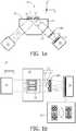
- FIGS 1a and 1bshow a general setup with of an optical biosensor 10 according to the present invention in a side view and a top view, respectively.
- the biosensor 10 setupcomprises a carrier 11 that may for example be made from glass or transparent plastic like polystyrene.
- the carrier 11comprises on its upper "contact surface” 12 a plurality of physically separated sample chambers or wells 2 in which sample fluids with target components to be detected (e.g. drugs, antibodies, DNA, etc.) can be provided.
- the samplesfurther comprise magnetic particles, for example superparamagnetic beads, wherein these particles are usually bound (via e.g. a coating with antibodies) as labels to the aforementioned target components.
- target particle 1For simplicity only the combination of target components and magnetic particles is shown in the Figures and will be called “target particle 1" in the following. It should be noted that instead of magnetic particles other label particles, for example electrically charged or fluorescent particles, could be used as well.
- the interface between the carrier 11 and the wells 2is usually coated with capture elements, e.g. antibodies, which can specifically bind to target particles.
- the sensor devicemay preferably comprise a magnetic field generator (not shown), for example an electromagnet with a coil and a core, for controllably generating a magnetic field at the contact surface 12 and in the adjacent space of the wells 2.
- a magnetic field generatorfor example an electromagnet with a coil and a core
- the target particles 1can be manipulated, i.e. be magnetized and particularly be moved (if magnetic fields with gradients are used).
- the sensor devicefurther comprises a light source 21 that generates an input light beam L1 which is transmitted into the carrier 11 through an "entrance window".
- a collimator lensmay be used to make the input light beam L1 parallel, and a pinhole may be used to control the beam diameter.
- the input light beam L1arrives in an investigation region 13 of the contact surface 12 at an angle larger than the critical angle ⁇ c of total internal reflection (TIR) and is therefore totally internally reflected in an "output light beam" L2.
- the output light beam L2leaves the carrier 11 through another surface ("exit window") and is detected by a light detector 31.
- the light detector 31determines the amount of light of the output light beam L2 (e.g. expressed by the light intensity of this light beam in the whole spectrum or a certain part of the spectrum). In the shown embodiment, this is done with the help of a detector plane P onto which the investigation region 13 is imaged.
- the detected image signals Iare evaluated and optionally monitored over an observation period by an evaluation and recording module 32 that is coupled to the detector 31.
- the described optical biosensorapplies optical means for the detection of target particles 1.
- the detection techniqueshould be surface-specific. As indicated above, this is achieved by using the principle of frustrated total internal reflection (FTIR). This principle is based on the fact that an evanescent wave penetrates (exponentially dropping in intensity) into the sample chambers 2 when the incident light beam L1 is totally internally reflected. If this evanescent wave then interacts with another medium like the bound target particles 1, part of the input light will be coupled into the sample fluid (this is called “frustrated total internal reflection"), and the reflected intensity will be reduced (while the reflected intensity will be 100% for a clean interface and no interaction).
- FTIRfrustrated total internal reflection
- medium A of the carrier 11can be glass and/or some transparent plastic with a typical refractive index of 1.52 or larger.
- Medium B in the sample chambers 2will be water-based and have a refractive index close to 1.3. This corresponds to a critical angle ⁇ c of 60°.
- Some applications of the described biosensorare the detection of a heart attack or the use of drugs-of-abuse.
- a biological assayBy binding or non-binding of the magnetic beads to the contact surface in a biological assay, multiple bio-markers can be detected in e.g. saliva or human blood plasma.
- very low detection limitsin the pM range and even less
- problemscan occur when detecting specific bio-markers simultaneously in one single reaction chamber.
- Some biological assaysshow interference when run at the same time.
- the optimal reaction conditions per assaymay vary, e.g. pH, usage of salts, sugars, specific buffer components etc. Therefore, it is required in some cases that each assay runs in its own reaction chamber or well 2, as shown in Figure 1 .
- the sensor surface of the investigation region 13that has to be imaged increases. Due to the chosen geometry of the optical plane, it is the easiest to extend the sensor surface along the length of the optical plane (y-direction in Figure 1 ), i.e. the investigation region 13 becomes asymmetric and very elongated in only one direction. This has severe consequences for the imaging system, as a much "longer" field of view is needed, while maintaining compact optics.
- the investigation region 13is imaged onto a CCD/CMOS camera using an imaging lens.
- a clear imagecan be obtained using a single cheap replicated collimator lens for an object size of about 2 ⁇ 1 mm 2 .
- a larger fieldneeds to be imaged by the image lens, and optical aberrations will partially destroy the image quality.
- Thiscan be overcome by a more complex lens design, using more than one lens element.
- a disadvantage of this methodis the increased cost of manufacturing since these individual lens elements need to be precisely aligned with respect to each other during the manufacturing process and multiple optical components are needed.
- the methodcan reasonably be applied only in imaging systems where the light beam originating from the object is a well-collimated, substantially parallel beam.
- thisis the case as the object is being imaged by total internal reflection (and not by for instance scattering) of a parallel input light beam L1, giving rise to a parallel output light beam L2 reaching the imaging lens.
- the object space numerical apertureis virtually zero in the biosensor application since the illumination is done using a well-collimated beam from a light source 21.
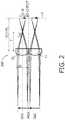
- the main operation principle of the proposed solutionis a subdivision of the main object (investigation region 13) into smaller sub-objects with corresponding sub-beams L2', L2" of the output light beam L2, thereby imaging each sub-object using a single lenslet LL, being part of a lenslet array or focusing optics 100.
- the resultis a series of sub-images on the detector plane P that can be stitched into one single image using standard and simple image processing techniques in the image processing device 32.
- Figure 2illustrates the operation principle for a special focusing optics 200 comprising two (identical) lenslets LL arranged adjacent to each other.
- the lenslets LLhave a diameter D, a focal length f, and individual optical axes OA1, OA2 (on the object side, i.e. left side in Figure 2 ) which are parallel to each other and to the main optical axis MOA of the whole focusing optics 200.
- the individual optical axes OA1, OA2are axes of rotational symmetry of the respective lenslets LL. Aberrations are minimized at the edges of the main image by a reduction of the maximum field angle (due to splitting up the object and imaging the sub-objects individually by separate lens elements).
- NAobject space numerical aperture
- magnification Mthere is an empty space or border between to sub-images. This empty space defines an upper limit for the magnification M that can be used given a finite dimension of the detector plane P. Obviously, the magnification M of the lenslets should be smaller than 1 (
- the total object sizeis given by H obj
- the number of lenslets LL to be usedis N > 2
- the magnificationis given by M (-1 ⁇ M ⁇ 0)
- the detector sizeis H det .
- the respective sub-imagesmay be shifted in the detector plane P such that the empty spaces between them are reduced to a minimum in order to allow for a larger magnification M.
- Thiscan be done in the optical domain using two approaches:
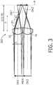
- Figures 3 and 4show the first approach 2A (lenslet arrays having tilted surfaces) for focusing optics 300 and 400 with two and three lenslets, respectively.
- Each sub-objectis imaged with a magnification smaller than 1 in order to prevent the sub-images to overlap. Consequently, there is an empty space between each sub-image, making the full image span unnecessarily larger than required.
- the lens arraymay be equipped with slightly tilted surfaces, refracting the sub-image towards the optical axis. This is tantamount to saying that the individual optical axes OA1', OA2', OA3' of the lenslets LL on the image side converge, wherein these axes are defined by the path of a light ray propagating along the (individual and main) optical axes OA1, OA2, OA3, MOA on the object side.
- the amount of tilt (angles ⁇ 1, ⁇ 2, ⁇ 3) to be introduced for each sub-imagedepends on the position of the sub-image with respect to the main optical axis MOA and on the magnification M.
- the sub-object widthis D.
- of the lenslets LLis smaller than 1, resulting in a series of sub-images with size D ⁇
- ⁇ wedgen ⁇ 1 ⁇ ⁇ (again for small angles ⁇ and ⁇ , with n being the refractive index of the lens material).
- nthe refractive index of the lens material
- Figure 5illustrates the second approach 2B (off-centered lenslets) for shifting the sub-images towards the main optical axis MOA.
- off-centered lenslets LLare used in the focusing optics 500, where the individual optical axes of the individual lenslets is offset with respect to the center of their sub-objects Oj (or sub-beams L2', L2", respectively).
- the required tilt that was introduced by the slanted surfaces in the previous methodis now incorporated in the imaging of the lenslets, where each sub-object Oj is imaged having an offset with respect to the optical axis OAj' of the corresponding lenslet LL.
Landscapes
- Physics & Mathematics (AREA)
- General Physics & Mathematics (AREA)
- Optics & Photonics (AREA)
- Health & Medical Sciences (AREA)
- Life Sciences & Earth Sciences (AREA)
- Chemical & Material Sciences (AREA)
- Analytical Chemistry (AREA)
- Biochemistry (AREA)
- General Health & Medical Sciences (AREA)
- Immunology (AREA)
- Pathology (AREA)
- Investigating Or Analysing Materials By Optical Means (AREA)
Description
- The invention relates to an optical biosensor comprising focusing optics.
- The
WO 2008/ 155716 discloses an optical biosensor in which an input light beam is totally internally reflected and the resulting output light beam is detected and evaluated with respect to the amount of target components at the reflection surface. When a plurality of analytes shall be tested in parallel in such or a similar biosensor, it is often necessary to provide the sample in spatially separated chambers. This increases the field of view that has to be surveyed, leading either to image deteriorations at the periphery of the imaged area or to complex optical systems. - The
US5412705 discloses an X-ray apparatus in which an array of lenses is used to map a fluorescent screen onto a plurality of image sensors Moreover, theJP2004317376 US20060289956 discloses a microlens structure that includes a wedge formed to support and tilt the microlens. The wedge results from heating a layer of patterned flowable material. The degree and direction of incline given to the wedge can be controlled in part by the type of patterning that is performed.US 20070054280 A1 discloses an optical micro-array reader system including a microchip array, a vertical cavity surface emitting laser array, a microlens array and a detector array. The microchip array includes multiple sample spots to be separately analyzed. The vertical cavity surface emitting laser array is disposed to simultaneously illuminate more than one of the multiple spots. The microlens array focuses fluorescences or other optical emissions from the sample spots onto the detector array.- Based on this situation it was an object of the present invention to provide means that allow the simultaneous detection of analytes in several distinct sample chambers of an optical biosensor.
- This object is achieved by an optical biosensor according to
claim 1. Preferred embodiments are disclosed in the dependent claims. - According to an aspect, focusing optics for an optical biosensor are disclosed, said optics comprising at least two focusing lenslets that are arranged adjacent to each other such that they image an incident parallel light beam, which is directed along a main optical axis of the focusing optics, onto a common plane.
- The term "lenslet" is used in this context to denote a lens that basically corresponds to a conventional optical lens, however with a size that is comparatively small. More precisely, the size of such a lenslet shall be smaller than the diameter of a light beam which shall be processed by the optics. Processing of the complete light beam hence requires the application of an array of lenslets. Preferably, the individual lenslets are fixed with respect to each other, for example by attachment to a common frame. The focusing optics can then be handled as a single object. The "main optical axis" is used to characterize the geometry of the focusing optics. Usually, this main optical axis corresponds to a symmetry axis of the focusing optics and/or it is parallel to the individual optical axes of the lenslets on the object side. In many cases the main optical axis corresponds to the mean of all individual optical axes. The "optical axis" of a refractive optical element is as usually defined as a direction along which there is some degree of rotational symmetry of the element (and, consequently, of its optical behavior). Moreover, the term "object side" is used to denote one side of a lenslet and of the complete focusing optics; during application, an object will typically be disposed on the "object side" of the focusing optics, while its image is generated at the opposite side, which is consequently called "image side".
- The invention relates to an optical biosensor comprising the following components:
- a) An investigation region being part of a surface adapted to be contacted by a sample
- b) A light source arranged to illuminate the investigation region
- c) Means for generating a substantially parallel "output light beam" that emanates from an investigation region and that is directed along an axis called "main optical axis". The investigation region will typically be a sub-region of some surface that can be contacted by a sample, wherein evaluation of an image of the investigation region will yield some information about said sample.
- d) A light detector with a light sensitive detector plane comprising an array of detector pixels. The light detector may comprise any suitable sensor or plurality of sensors by which light of a given spectrum can be detected, for example photodiodes, photo resistors, photocells, a CCD/CMOS chip, or a photo multiplier tube.
- e) Focusing optics comprising at least two focusing lenslets that have each an individual optical axis and that are arranged adjacent to each other such that they image the output parallel light beam onto the detector plane on an image side of the at least two focusing lenslets, the main optical axis corresponding to the mean of all individual optical axes, wherein the individual optical axes of the lenslets on the image side are converging. With other words, the focusing optics of the optical biosensor is a focusing optics according to the first aspect of the invention with its object side being oriented towards the investigation region.
- According to a third aspect, a method for imaging an investigation region onto the detector plane of a light detector of an optical biosensor is disclosed, said method comprising the following steps:
- a) Generating a substantially parallel output light beam that emanates from the investigation region and propagates along an axis called "main optical axis".
- b) Focusing adjacent sub-beams of the aforementioned output light beam separately by lenslets of a focusing optics onto the detector plane.
- The focusing optics, the optical biosensor, and the method according to the above aspects have in common to allow the focusing of several sub-beams of a large parallel output light beam onto different zones of a detector plane. An output light beam with a large diameter can hence be processed while at the same time optical distortions in peripheral areas are avoided because processing is done with respect to sub-beams of limited extension. This allows to survey a comparatively large investigation region of an optical biosensor with a high accuracy of the optical measurements but without a complex optical system that might be difficult to adjust. Instead, the focusing optics comprising a plurality of lenslets arranged adjacent to each other suffices.
- In the following, further developments will be described that relate to the focusing optics, the optical biosensor, and the method according to the above aspects.
- The parallel output light beam that emanates from the investigation region and that is processed by the focusing optics may in general be generated in many different ways, for example by transmission of light through the investigation region. In a preferred embodiment of the invention, the output light beam is generated by total internal reflection of an input light beam at the investigation region. The input light beam can be generated by a light source of the optical biosensor, for example a laser or a light emitting diode (LED), optionally provided with some optics for shaping and directing the input light beam.
- The light detector comprises a plurality of individual detector units, which will as usually be called "pixels" in the following. Such a pixilated light detector may particularly be realized by an image sensor, for example a CCD or CMOS device as it is known from digital cameras. A plurality of detector pixels allows to evaluate the information comprised by the output light beam in a spatially resolved way with respect to the investigation region.
- According to another embodiment, the biosensor comprises an image processing device, for example a computer with associated software for digital image processing, said image processing device being able to process images generated by different lenslets. In particularly, the image processing device may be adapted to combine images generated by different lenslets. This approach is useful if the individual images generated by different lenslets are separated from each other in the detector plane by borders which comprise no useful information. The areas of the detector plane comprising valid images can then be isolated and stitched together by the image processing device.
- The investigation region may preferably cover a plurality of physically separated sample chambers, called "wells", that can separately provide samples. Such wells may for example be realized on the surface of a (transparent) carrier. The provision of separated wells allows to prepare one or more samples under different conditions and to evaluate these preparations in parallel. The plurality of separated wells typically implies a comparatively large, elongated shape of the investigation region. Nevertheless, this investigation region can accurately be imaged onto the detector plane with the help of the focusing optics.
- Focusing optics with the required imaging characteristics (i.e. imaging a parallel beam onto a common plane) can for example be realized by lenslets with their individual optical axes being parallel on the object side.
- In order to avoid a mutual overlap of the images generated by the different lenslets, the magnification M of the lenslets is preferably chosen to be smaller than one, i.e. |M| < 1. It should however be noted that also cases in which the magnification is larger than 1 will work, though some parts of the images will then be rendered useless due to an overlap (this may be tolerable if the sample chamber is appropriately designed).
- In a preferred embodiment of to the invention, the image generated by at least one lenslet is shifted (with respect to an extension of its individual optical axis from the object to the image side) towards a selected axis. In case the lenslets have a magnification smaller than one, "useless" borders around the images generated by the individual lenslets can be avoided by shifting these images in the detector plane towards the mentioned selected axis. The selected axis will often be chosen to correspond to the main optical axis of the focusing optics.
- The aforementioned shift of the lenslet images can be realized in different ways. According to a first approach, it is achieved by making the individual optical axes of the lenslets on the image side of the focusing optics convergence (towards the selected axis). In this context, the "individual optical axis on the image side of a lenslet" is defined by the image-side path of a light ray that comes along the individual optical axis on the object side of the lenslet.
- In a preferred embodiment the (preferably planar) facet of at least one lenslet on the image side is tilted with respect to the main optical axis. This implies that the aforementioned individual optical axis of said lenslet on its image side is also tilted, which allows to shift the image generated by the lenslet in the detector plane.
- According to a further development of the aforementioned embodiment, a plurality of lenslets has such tilted surfaces on their image side, wherein the tilting angle increases with the distance of the lenslet from a selected axis (eg. from the main optical axis of the focusing optics). With this embodiment, convergent individual optical axes of the lenslets on the image side can be realized, and hence the shifting of the lenslet images towards the selected axis.
- According to another embodiment of the invention, at least one lenslet is off-centre with respect to the sub-beam of the output light beam which this lenslet is exposed to. This means that the individual optical axis of this lenslet does not coincide with the middle axis of said sub-beam. With a plurality of such off-centre lenslets, convergence of the lenslet images towards a selected axis can be realized.
- The invention further relates to the use of the focusing optics for the biosensor described above for molecular diagnostics, biological sample analysis, or chemical sample analysis, food analysis, and/or forensic analysis. Molecular diagnostics may for example be accomplished with the help of magnetic beads or fluorescent particles that are directly or indirectly attached to target molecules.
- These and other aspects of the invention will be apparent from and elucidated with reference to the embodiment(s) described hereinafter. These embodiments will be described by way of example with the help of the accompanying drawings in which:
- Figure la schematically illustrates an optical biosensor according to the invention in a side view;
Figure 1b shows the biosensor ofFigure 1a in a top view;Figure 2 illustrates an embodiment of focusing optics comprising two adjacent lenslets;Figure 3 illustrates an embodiment of focusing optics comprising two adjacent lenslets with slanted surfaces on the image side;Figure 4 illustrates an embodiment of focusing optics comprising three lenslets having differently slanted surfaces on the image side;Figure 5 illustrates an embodiment of focusing optics with off-centred lenslets.- Like reference numbers or numbers differing by integer multiples of 100 refer in the Figures to identical or similar components.
- Though the present invention will in the following be described with respect to a particular setup (using magnetic particles and frustrated total internal reflection as measurement principle), it is not limited to such an approach and can favorably be used in many different applications and setups.
Figures 1a and 1b show a general setup with of anoptical biosensor 10 according to the present invention in a side view and a top view, respectively. Thebiosensor 10 setup comprises acarrier 11 that may for example be made from glass or transparent plastic like polystyrene. Thecarrier 11 comprises on its upper "contact surface" 12 a plurality of physically separated sample chambers orwells 2 in which sample fluids with target components to be detected (e.g. drugs, antibodies, DNA, etc.) can be provided. The samples further comprise magnetic particles, for example superparamagnetic beads, wherein these particles are usually bound (via e.g. a coating with antibodies) as labels to the aforementioned target components. For simplicity only the combination of target components and magnetic particles is shown in the Figures and will be called "target particle 1" in the following. It should be noted that instead of magnetic particles other label particles, for example electrically charged or fluorescent particles, could be used as well. The interface between thecarrier 11 and thewells 2 is usually coated with capture elements, e.g. antibodies, which can specifically bind to target particles.- The sensor device may preferably comprise a magnetic field generator (not shown), for example an electromagnet with a coil and a core, for controllably generating a magnetic field at the
contact surface 12 and in the adjacent space of thewells 2. With the help of this magnetic field, thetarget particles 1 can be manipulated, i.e. be magnetized and particularly be moved (if magnetic fields with gradients are used). Thus it is for example possible to attracttarget particles 1 to thecontact surface 12 in order to accelerate their binding to said surface, or to wash unbound target particles away from the contact surface before a measurement. - The sensor device further comprises a
light source 21 that generates an input light beam L1 which is transmitted into thecarrier 11 through an "entrance window". Aslight source 21, e.g. a commercial CD (λ = 780 nm), DVD (λ = 658 nm), or BD (λ = 405 nm) laser-diode, or a collimated LED source can be used. A collimator lens may be used to make the input light beam L1 parallel, and a pinhole may be used to control the beam diameter. The input light beam L1 arrives in aninvestigation region 13 of thecontact surface 12 at an angle larger than the critical angle θc of total internal reflection (TIR) and is therefore totally internally reflected in an "output light beam" L2. The output light beam L2 leaves thecarrier 11 through another surface ("exit window") and is detected by alight detector 31. Thelight detector 31 determines the amount of light of the output light beam L2 (e.g. expressed by the light intensity of this light beam in the whole spectrum or a certain part of the spectrum). In the shown embodiment, this is done with the help of a detector plane P onto which theinvestigation region 13 is imaged. The detected image signals I are evaluated and optionally monitored over an observation period by an evaluation andrecording module 32 that is coupled to thedetector 31. - The described optical biosensor applies optical means for the detection of
target particles 1. For eliminating or at least minimizing the influence of background (e.g. of the sample fluid, such as saliva, blood, etc.), the detection technique should be surface-specific. As indicated above, this is achieved by using the principle of frustrated total internal reflection (FTIR). This principle is based on the fact that an evanescent wave penetrates (exponentially dropping in intensity) into thesample chambers 2 when the incident light beam L1 is totally internally reflected. If this evanescent wave then interacts with another medium like the boundtarget particles 1, part of the input light will be coupled into the sample fluid (this is called "frustrated total internal reflection"), and the reflected intensity will be reduced (while the reflected intensity will be 100% for a clean interface and no interaction). Depending on the amount of disturbance, i.e. the amount of target particles on or very near (within about 200 nm) to the TIR surface (not in the rest of the sample chambers 2), the reflected intensity will drop accordingly. This intensity drop is a direct measure for the amount of boundtarget particles 1, and therefore for the concentration of target particles in the sample. For the materials of a typical application, medium A of thecarrier 11 can be glass and/or some transparent plastic with a typical refractive index of 1.52 or larger. Medium B in thesample chambers 2 will be water-based and have a refractive index close to 1.3. This corresponds to a critical angle θc of 60°. - Advantages of the described optical read-out combined with magnetic labels for actuation are the following:
- Cheap cartridge: The
carrier 11 can consist of a relatively simple, injection-molded piece of polymer material. - Actuation and sensing are orthogonal: Magnetic actuation of the target particles (by large magnetic fields and magnetic field gradients) does not influence the sensing process. The optical method therefore allows a continuous monitoring of the signal during actuation. This provides a lot of insights into the assay process and it allows easy kinetic detection methods based on signal slopes.
- Large multiplexing possibilities for multi-analyte testing: The
contact surface 12 in a disposable cartridge can be optically scanned over a large area. Alternatively, large-area imaging is possible allowing a large detection array. Such an array (located on an optical transparent surface) can be made by e.g. ink-jet printing of different binding molecules on the optical surface. - The method also enables high-throughput testing in (specifically designed) well-plates by using multiple beams and multiple detectors and multiple actuation magnets (either mechanically moved or electro-magnetically actuated).
- Some applications of the described biosensor are the detection of a heart attack or the use of drugs-of-abuse. By binding or non-binding of the magnetic beads to the contact surface in a biological assay, multiple bio-markers can be detected in e.g. saliva or human blood plasma. By using (frustrated) total internal reflection as a detection technique in combination with magnetic actuated beads, very low detection limits (in the pM range and even less) are achieved in combination with short measurement/assay times. However, if multiple bio-assays would be run at the same time, problems can occur when detecting specific bio-markers simultaneously in one single reaction chamber. Some biological assays show interference when run at the same time. Also the optimal reaction conditions per assay may vary, e.g. pH, usage of salts, sugars, specific buffer components etc. Therefore, it is required in some cases that each assay runs in its own reaction chamber or well 2, as shown in
Figure 1 . - As the
wells 2 need to have walls to confine the liquids, buffers etc., much more space is needed at the sensor surface to accommodate all bio-assays separately. This means that the sensor surface of theinvestigation region 13 that has to be imaged increases. Due to the chosen geometry of the optical plane, it is the easiest to extend the sensor surface along the length of the optical plane (y-direction inFigure 1 ), i.e. theinvestigation region 13 becomes asymmetric and very elongated in only one direction. This has severe consequences for the imaging system, as a much "longer" field of view is needed, while maintaining compact optics. - In practical realizations of the
biosensor 10, theinvestigation region 13 is imaged onto a CCD/CMOS camera using an imaging lens. A clear image can be obtained using a single cheap replicated collimator lens for an object size of about 2×1 mm2. As explained above, there is a need to increase the object size to a more elongated area with typical dimensions of 6.5×1 mm2 or even larger. As a result a larger field needs to be imaged by the image lens, and optical aberrations will partially destroy the image quality. This can be overcome by a more complex lens design, using more than one lens element. A disadvantage of this method is the increased cost of manufacturing since these individual lens elements need to be precisely aligned with respect to each other during the manufacturing process and multiple optical components are needed. - To overcome the described problems, it is proposed here to use only a single lens element, consisting of a series of smaller lenslets. This lenslet array can for instance be produced using standard plastic injection moulding techniques. As a result the proposed method uses only one single lens element and only requires course alignment for correct image focusing.
- It should be noted that the method can reasonably be applied only in imaging systems where the light beam originating from the object is a well-collimated, substantially parallel beam. For the application shown in
Figure 1 , this is the case as the object is being imaged by total internal reflection (and not by for instance scattering) of a parallel input light beam L1, giving rise to a parallel output light beam L2 reaching the imaging lens. In technical terms: the object space numerical aperture is virtually zero in the biosensor application since the illumination is done using a well-collimated beam from alight source 21. - Hence the main operation principle of the proposed solution is a subdivision of the main object (investigation region 13) into smaller sub-objects with corresponding sub-beams L2', L2" of the output light beam L2, thereby imaging each sub-object using a single lenslet LL, being part of a lenslet array or focusing
optics 100. The result is a series of sub-images on the detector plane P that can be stitched into one single image using standard and simple image processing techniques in theimage processing device 32. Figure 2 illustrates the operation principle for a special focusingoptics 200 comprising two (identical) lenslets LL arranged adjacent to each other. The lenslets LL have a diameter D, a focal length f, and individual optical axes OA1, OA2 (on the object side, i.e. left side inFigure 2 ) which are parallel to each other and to the main optical axis MOA of the whole focusingoptics 200. As usual, the individual optical axes OA1, OA2 are axes of rotational symmetry of the respective lenslets LL. Aberrations are minimized at the edges of the main image by a reduction of the maximum field angle (due to splitting up the object and imaging the sub-objects individually by separate lens elements).- The proposed method works as long as the object space numerical aperture (NA) is virtually zero, i.e. light originating from a single sub-object is allowed to be imaged by only one lenslet LL. Otherwise multiple images of a single sub-object would be imaged onto the detector plane P, making the imaging useless.
- It should further be noted that there is an empty space or border between to sub-images. This empty space defines an upper limit for the magnification M that can be used given a finite dimension of the detector plane P. Obviously, the magnification M of the lenslets should be smaller than 1 (|M| < 1) to prevent that two images overlap.
- In a general situation, the total object size is given by Hobj, the number of lenslets LL to be used is N > 2, the magnification is given by M (-1 < M < 0), and the detector size is Hdet. Two procedures are then possible:
- 1. Stitching the digitalized images I in software using image processing. The upper limit of the magnification is then given by |M|max with -|M|max < M < 0 and:

- 2. Shifting the sub-images towards the main optical axis using imaging optics. In this case the full sensor surface can be used and the maximum magnification is then simply given by:

- These procedures will now be described in more detail, starting with the stitching of sub-images. On the detector plane P, an array of sub-images of width D·M is formed by the
lenslet array 200, as illustrated inFigure 2 . These sub-images may be stitched together by using known image processing techniques. The actually used sensor area is in this case larger than the net image area, due to the empty spaces in between the sub-images. As a result the optical magnification M that can be used is limited. - In the second procedure, the respective sub-images may be shifted in the detector plane P such that the empty spaces between them are reduced to a minimum in order to allow for a larger magnification M. This can be done in the optical domain using two approaches:
- 2A. Using lenslets LL centered with respect to the center of the sub-objects, but having a tilted second surface where the tilt angle of the slanted sub-surfaces increases when going away from the main optical axis of the lenslet array (cf.
Figures 3 ,4 ). - 2B. Using lenslets LL off-centered with respect to the center of the sub-objects (
Figures 5 ). Figures 3 and4 show the first approach 2A (lenslet arrays having tilted surfaces) for focusingoptics 
- Each sub-object is imaged with a magnification smaller than 1 in order to prevent the sub-images to overlap. Consequently, there is an empty space between each sub-image, making the full image span unnecessarily larger than required. In order to get rid of these empty spaces in the image, the lens array may be equipped with slightly tilted surfaces, refracting the sub-image towards the optical axis. This is tantamount to saying that the individual optical axes OA1', OA2', OA3' of the lenslets LL on the image side converge, wherein these axes are defined by the path of a light ray propagating along the (individual and main) optical axes OA1, OA2, OA3, MOA on the object side.
- The amount of tilt (angles β1, β2, β3) to be introduced for each sub-image depends on the position of the sub-image with respect to the main optical axis MOA and on the magnification M. For each sub-image j the required tilt angle βj of the lens surface may be calculated as follows (wherein j = 0 corresponds with the sub-image closest to the main optical axis MOA; when going to the outer rim of the object/lens array, j increases with 1 for each subsequent lenslet):
The sub-object width is D. The magnification |M| of the lenslets LL is smaller than 1, resulting in a series of sub-images with size D·|M|, separated from each other over a distance D. Consequently there is an empty space between each sub-image of width D·(1-|M|). In order to make a single closed image, all sub-images have to be shifted towards the main optical axis MOA. For the first sub-image the shift angle Δα1 is calculated as follows:


- Of course the same method can be used for making larger subdivision of the main image. Sub-images further away from the main optical axis should be shifted over a larger angle towards the optical axis. As long as the small-angle approximation is valid, this shift for the other sub-images is equal to:

- This lateral shift of the sub-images can be obtained by slightly tilting the lenslets' facets on the image side, such that it acts as a wedge, with a ray deviation of

Figure 4 ) according to:
Figure 5 illustrates the second approach 2B (off-centered lenslets) for shifting the sub-images towards the main optical axis MOA. Here off-centered lenslets LL are used in the focusingoptics 500, where the individual optical axes of the individual lenslets is offset with respect to the center of their sub-objects Oj (or sub-beams L2', L2", respectively). The required tilt that was introduced by the slanted surfaces in the previous method is now incorporated in the imaging of the lenslets, where each sub-object Oj is imaged having an offset with respect to the optical axis OAj' of the corresponding lenslet LL. InFigure 5 , the position of the individual optical axes OA1', OA2' of the respective lenslets LL is given by yj. Here the magnification is M, and the size of each sub-object is given by h = Hobj/N.- From geometry considerations using the hatched triangle in
Figure 5 one can deduce:
- This leads to the following equation for yj, giving the position of the optical axis of each lenslet with respect to the central main optical axis MOA of the lenslet array:

- It should be noted that j > 1 in this equation. Since the lenslet array is symmetrical with respect to the main optical axis MOA the equation can be rewritten as:

- While the invention was described above with reference to particular embodiments, various modifications and extensions are possible, for example:
- Molecular targets often determine the concentration and/or presence of larger moieties, e.g. cells, viruses, or fractions of cells or viruses, tissue extract, etc.
- In addition to molecular assays, also larger moieties can be detected with sensor devices according to the invention, e.g. cells, viruses, or fractions of cells or viruses, tissue extract, etc.
- The detection can occur with or without scanning of the sensor element with respect to the sensor surface.
- Measurement data can be derived as an end-point measurement, as well as by recording signals kinetically or intermittently.
- The particles serving as labels can be detected directly by the sensing method. As well, the particles can be further processed prior to detection. An example of further processing is that materials are added or that the (bio)chemical or physical properties of the label are modified to facilitate detection.
- The device and method can be used with several biochemical assay types, e.g. binding/unbinding assay, sandwich assay, competition assay, displacement assay, enzymatic assay, etc. It is especially suitable for DNA detection because large scale multiplexing is easily possible and different oligos can be spotted via ink-jet printing on a substrate.
- The device and method are suited for sensor multiplexing (i.e. the parallel use of different sensors and sensor surfaces), label multiplexing (i.e. the parallel use of different types of labels) and chamber multiplexing (i.e. the parallel use of different reaction chambers).
- The device and method can be used as rapid, robust, and easy to use point-of-care biosensors for small sample volumes. The reaction chamber can be a disposable item to be used with a compact reader, containing the one or more field generating means and one or more detection means. Also, the device, methods and systems of the present invention can be used in automated high-throughput testing. In this case, the reaction chamber is e.g. a well-plate or cuvette, fitting into an automated instrument.
- With nano-particles are meant particles having at least one dimension ranging between 3 nm and 5000 nm, preferably between 10 nm and 3000 nm, more preferred between 50 nm and 1000 nm.
- Finally it is pointed out that in the present application the term "comprising" does not exclude other elements or steps, that "a" or "an" does not exclude a plurality, and that a single processor or other unit may fulfill the functions of several means. The invention resides in each and every novel characteristic feature and each and every combination of characteristic features. Moreover, reference signs in the claims shall not be construed as limiting their scope.


Claims (10)
- Optical biosensor (10) comprising:a) an investigation region (13) being part of a surface adapted to be contacted by a sample;b) a light source (21) arranged to illuminate the investigation region;c) means (21, 12) for generating a substantially parallel output light beam (L2) that emanates from an investigation region (13) and that is directed along a main optical axis (MOA);d) a light detector (31) with a detector plane (P) comprising an array of detector pixels;e) focusing optics (100-500) comprising at least two focusing lenslets (LL) that have each an individual optical axis (OA1, OA2) and that are arranged adjacent to each other such that they image the output parallel light beam (L2) onto said detector plane (P) on an image side of the at least two focusing lenslets (LL), said main optical axis (MOA) corresponding to the mean of all individual optical axes (OA1, OA2),characterized in that the individual optical axes (OA1', OA2', OA3') of the lenslets (LL) on the image side are converging.
- Optical biosensor (10) according to claim 1,
characterized in that the individual optical axes (OA1, OA2, OA3) of the lenslets (LL) are parallel to each other on the object side. - Optical biosensor (10) according to claim 1,
characterized in that the magnification of each lenslet (LL) is smaller than one. - Optical biosensor (10) according to claim 1,
characterized in that the image generated by at least one lenslet (LL) is shifted towards a selected axis (MOA). - Optical biosensor (10) according to claim 1,characterized in that the output facet of at least one lenslet (LL) on the image side is tilted with respect to the main optical axis (MOA).
- Optical biosensor (10) according to claim 5,
characterized in that the tilting angle (β1, β2, β3) increases for different lenslets (LL) with their distance from a selected axis (MOA). - Optical biosensor (10) according to claim 1,
characterized in that at least one lenslet (LL) is off-centre with respect to the sub-beam (L2', L2") of the output light beam (L2) it receives. - Optical biosensor (10) according to claim 1,
characterized in that the output light beam (L2) is generated by total internal reflection of an input light beam (L1) at the investigation region (13). - Optical biosensor (10) according to claim 1,
characterized in that the biosensor (10) comprises an image processing device (32) for processing images generated by different lenslets (LL). - Optical biosensor (10) according to claim 1,
characterized in that the investigation region (13) covers a plurality of wells (2) that can each provide a sample.
Priority Applications (1)
| Application Number | Priority Date | Filing Date | Title |
|---|---|---|---|
| EP10730242.4AEP2446249B1 (en) | 2009-06-24 | 2010-06-21 | Optical biosensor with focusing optics |
Applications Claiming Priority (3)
| Application Number | Priority Date | Filing Date | Title |
|---|---|---|---|
| EP09163571 | 2009-06-24 | ||
| PCT/IB2010/052786WO2010150167A1 (en) | 2009-06-24 | 2010-06-21 | Optical biosensor with focusing optics |
| EP10730242.4AEP2446249B1 (en) | 2009-06-24 | 2010-06-21 | Optical biosensor with focusing optics |
Publications (2)
| Publication Number | Publication Date |
|---|---|
| EP2446249A1 EP2446249A1 (en) | 2012-05-02 |
| EP2446249B1true EP2446249B1 (en) | 2020-08-05 |
Family
ID=42455329
Family Applications (1)
| Application Number | Title | Priority Date | Filing Date |
|---|---|---|---|
| EP10730242.4AActiveEP2446249B1 (en) | 2009-06-24 | 2010-06-21 | Optical biosensor with focusing optics |
Country Status (4)
| Country | Link |
|---|---|
| US (1) | US8670123B2 (en) |
| EP (1) | EP2446249B1 (en) |
| CN (1) | CN102803930B (en) |
| WO (1) | WO2010150167A1 (en) |
Families Citing this family (15)
| Publication number | Priority date | Publication date | Assignee | Title |
|---|---|---|---|---|
| EP2392144A1 (en)* | 2009-01-29 | 2011-12-07 | Dolby Laboratories Licensing Corporation | Methods and devices for sub-sampling and interleaving multiple images, eg stereoscopic |
| WO2012101539A1 (en)* | 2011-01-27 | 2012-08-02 | Koninklijke Philips Electronics N.V. | Localization of detection spots |
| WO2013035009A1 (en) | 2011-09-06 | 2013-03-14 | Koninklijke Philips Electronics N.V. | Optical biosensor with a plurality of sensors regions |
| WO2014013372A1 (en)* | 2012-07-18 | 2014-01-23 | Koninklijke Philips N.V. | Processing of a sample fluid with target components |
| AU2015374335B2 (en) | 2014-12-23 | 2018-03-29 | Apple Inc. | Optical inspection system and method including accounting for variations of optical path length within a sample |
| CN107430263B (en) | 2014-12-23 | 2020-12-01 | 苹果公司 | Confocal inspection system with average illumination path and average collection path |
| WO2016106350A1 (en) | 2014-12-23 | 2016-06-30 | Bribbla Dynamics Llc | Confocal inspection system having non-overlapping annular illumination and collection regions |
| WO2017040431A1 (en) | 2015-09-01 | 2017-03-09 | Bribbla Dynamics Llc | Reference switch architectures for noncontact sensing of substances |
| US9801587B2 (en) | 2015-10-19 | 2017-10-31 | Garmin Switzerland Gmbh | Heart rate monitor with time varying linear filtering |
| EP4589271A3 (en)* | 2016-04-21 | 2025-07-30 | Apple Inc. | Optical system for reference switching |
| US11579080B2 (en) | 2017-09-29 | 2023-02-14 | Apple Inc. | Resolve path optical sampling architectures |
| EP3752873A1 (en) | 2018-02-13 | 2020-12-23 | Apple Inc. | Integrated photonics device having integrated edge outcouplers |
| CN116057454A (en) | 2020-09-09 | 2023-05-02 | 苹果公司 | Optical system for noise mitigation |
| CN113405703B (en)* | 2021-06-16 | 2024-04-09 | 哲弗智能系统(上海)有限公司 | Optical sensor and fire alarm device |
| US12336797B2 (en) | 2022-10-26 | 2025-06-24 | Garmin International, Inc. | Wrist-worn electronic device with optical cardiac monitor |
Citations (4)
| Publication number | Priority date | Publication date | Assignee | Title |
|---|---|---|---|---|
| FR2737832A1 (en)* | 1995-08-11 | 1997-02-14 | Jean Flinois | Image coding and compression device for stereoscopic vision - compresses left and right hand images either vertically or horizontally with coding performed to generate image in same format as original images, with vision system e.g. spectacles allowing viewing of stereoscopic image |
| US20060289956A1 (en)* | 2005-06-28 | 2006-12-28 | Micron Technology, Inc. | Process for creating tilted microlens |
| US20070054280A1 (en)* | 2005-09-08 | 2007-03-08 | Intel Corporation | High throughput optical micro-array reader capable of variable pitch and spot size array processing for genomics and proteomics |
| WO2008155716A1 (en)* | 2007-06-21 | 2008-12-24 | Koninklijke Philips Electronics N. V. | Microelectronic sensor device for detecting label particles |
Family Cites Families (28)
| Publication number | Priority date | Publication date | Assignee | Title |
|---|---|---|---|---|
| CA1321488C (en)* | 1987-08-22 | 1993-08-24 | Martin Francis Finlan | Biological sensors |
| US5291334A (en) | 1992-01-30 | 1994-03-01 | United Technologies Corporation | Micro-lens panoramic imager |
| US5233174A (en)* | 1992-03-11 | 1993-08-03 | Hughes Danbury Optical Systems, Inc. | Wavefront sensor having a lenslet array as a null corrector |
| JPH06205768A (en) | 1992-08-18 | 1994-07-26 | Philips Electron Nv | X-ray examination apparatus |
| US5493391A (en)* | 1994-07-11 | 1996-02-20 | Sandia Corporation | One dimensional wavefront distortion sensor comprising a lens array system |
| US5629765A (en)* | 1995-12-15 | 1997-05-13 | Adaptive Optics Associates, Inc. | Wavefront measuring system with integral geometric reference (IGR) |
| GB9810350D0 (en)* | 1998-05-14 | 1998-07-15 | Ciba Geigy Ag | Organic compounds |
| GB9906929D0 (en)* | 1999-03-26 | 1999-05-19 | Univ Glasgow | Assay system |
| US6184974B1 (en)* | 1999-07-01 | 2001-02-06 | Wavefront Sciences, Inc. | Apparatus and method for evaluating a target larger than a measuring aperture of a sensor |
| US6376819B1 (en) | 1999-07-09 | 2002-04-23 | Wavefront Sciences, Inc. | Sub-lens spatial resolution Shack-Hartmann wavefront sensing |
| EP1311824A4 (en) | 2000-06-25 | 2010-12-08 | Affymetrix Inc | Optically active substrates |
| JP2003121777A (en)* | 2001-10-18 | 2003-04-23 | Sony Corp | Illuminator using lens array and picture display device |
| US7135686B1 (en)* | 2002-11-19 | 2006-11-14 | Grady John K | Low noise x-ray detector for fluoroscopy |
| US7414712B2 (en)* | 2003-02-13 | 2008-08-19 | University Of Rochester | Large dynamic range Shack-Hartmann wavefront sensor |
| US7151598B2 (en)* | 2003-04-04 | 2006-12-19 | Vladimir Poponin | Method and apparatus for enhanced nano-spectroscopic scanning |
| JP2004317376A (en) | 2003-04-17 | 2004-11-11 | Nikon Corp | A wavefront measuring method, a wavefront measuring apparatus, a method for adjusting an imaging optical system, and a method for manufacturing a semiconductor exposure apparatus. |
| US7084966B2 (en)* | 2003-10-20 | 2006-08-01 | Infineon Technologies Ag | Optical measurement of device features using lenslet array illumination |
| US20060227328A1 (en)* | 2005-04-08 | 2006-10-12 | Vanwiggeren Gregory D | Light-sensing system that uses light guides |
| EP1910809A1 (en)* | 2005-07-21 | 2008-04-16 | Koninklijke Philips Electronics N.V. | Device for detection of excitation using a multiple spot arrangement |
| CN101278186A (en) | 2005-10-03 | 2008-10-01 | 皇家飞利浦电子股份有限公司 | Biosensors with improved sensitivity |
| US7286295B1 (en) | 2005-11-30 | 2007-10-23 | Sandia Corporation | Microoptical compound lens |
| US7463353B2 (en)* | 2006-05-31 | 2008-12-09 | Uchicago Argonne, Llc | Modular, micro-scale, optical array and biodetection system |
| JP2008209712A (en)* | 2007-02-27 | 2008-09-11 | Victor Co Of Japan Ltd | Optical element and image stabilizer device |
| US7978411B2 (en)* | 2007-05-08 | 2011-07-12 | Micron Technology, Inc. | Tetraform microlenses and method of forming the same |
| CN201133897Y (en)* | 2007-12-18 | 2008-10-15 | 陈晓汀 | Multi-light source multichannel measuring system |
| US7988293B2 (en)* | 2008-11-14 | 2011-08-02 | AMO Wavefront Sciences LLC. | Method of qualifying light spots for optical measurements and measurement instrument employing method of qualifying light spots |
| WO2010122547A1 (en)* | 2009-04-20 | 2010-10-28 | Bio-Rad Laboratories Inc. | Non-scanning surface plasmon resonance ( spr) system |
| US8358366B1 (en)* | 2010-05-28 | 2013-01-22 | Adobe Systems Incorporate | Methods and apparatus for high-speed digital imaging |
- 2010
- 2010-06-21EPEP10730242.4Apatent/EP2446249B1/enactiveActive
- 2010-06-21WOPCT/IB2010/052786patent/WO2010150167A1/enactiveApplication Filing
- 2010-06-21CNCN201080028082.0Apatent/CN102803930B/enactiveActive
- 2010-06-21USUS13/379,721patent/US8670123B2/enactiveActive
Patent Citations (4)
| Publication number | Priority date | Publication date | Assignee | Title |
|---|---|---|---|---|
| FR2737832A1 (en)* | 1995-08-11 | 1997-02-14 | Jean Flinois | Image coding and compression device for stereoscopic vision - compresses left and right hand images either vertically or horizontally with coding performed to generate image in same format as original images, with vision system e.g. spectacles allowing viewing of stereoscopic image |
| US20060289956A1 (en)* | 2005-06-28 | 2006-12-28 | Micron Technology, Inc. | Process for creating tilted microlens |
| US20070054280A1 (en)* | 2005-09-08 | 2007-03-08 | Intel Corporation | High throughput optical micro-array reader capable of variable pitch and spot size array processing for genomics and proteomics |
| WO2008155716A1 (en)* | 2007-06-21 | 2008-12-24 | Koninklijke Philips Electronics N. V. | Microelectronic sensor device for detecting label particles |
Also Published As
| Publication number | Publication date |
|---|---|
| US20120147377A1 (en) | 2012-06-14 |
| CN102803930B (en) | 2016-04-27 |
| WO2010150167A1 (en) | 2010-12-29 |
| CN102803930A (en) | 2012-11-28 |
| EP2446249A1 (en) | 2012-05-02 |
| US8670123B2 (en) | 2014-03-11 |
Similar Documents
| Publication | Publication Date | Title |
|---|---|---|
| EP2446249B1 (en) | Optical biosensor with focusing optics | |
| EP2092339B1 (en) | Microelectronic sensor device for detecting label particles | |
| US8686376B2 (en) | Microarray characterization system and method | |
| CN102549445B (en) | Biosensor system for single particle detection | |
| US7292333B2 (en) | Optical interrogation system and method for 2-D sensor arrays | |
| US7799558B1 (en) | Ligand binding assays on microarrays in closed multiwell plates | |
| WO2008155716A1 (en) | Microelectronic sensor device for detecting label particles | |
| EP2208053A2 (en) | Microelectronic optical evanescent field sensor | |
| WO2009019619A1 (en) | Microelectronic sensor device for optical examinations in a sample medium | |
| EP2174114A2 (en) | Microelectronic sensor device for optical examinations with total internal reflection | |
| CN102713571B (en) | There is the sensor device of imaging optic element | |
| US20110235037A1 (en) | Sensor device for detecting target particles by frustrated total internal reflection | |
| US7863037B1 (en) | Ligand binding assays on microarrays in closed multiwell plates | |
| GB2515490A (en) | An aperture array substrate device, a detection system and a method for detecting analytes in a sample | |
| JP5542067B2 (en) | Molecular diagnostic system based on evanescent irradiation and fluorescence | |
| KR20140021620A (en) | Compact label free imaging system | |
| WO2009007888A1 (en) | An opto-mechanical arrangement for providing optical access to a sample chamber | |
| JP2010066212A (en) | Measurement apparatus, and method of measuring object to be observed | |
| EP1972927A1 (en) | Microelectronic sensor device for detecting label particles | |
| EP2163885A1 (en) | Microarray characterization system and method | |
| WO2011102981A1 (en) | High resolution label free imaging | |
| US20130094019A1 (en) | Sample carrier with light refracting structures | |
| WO2009004538A1 (en) | Microelectronic sensor device for examinations in a carrier |
Legal Events
| Date | Code | Title | Description |
|---|---|---|---|
| PUAI | Public reference made under article 153(3) epc to a published international application that has entered the european phase | Free format text:ORIGINAL CODE: 0009012 | |
| 17P | Request for examination filed | Effective date:20120124 | |
| AK | Designated contracting states | Kind code of ref document:A1 Designated state(s):AL AT BE BG CH CY CZ DE DK EE ES FI FR GB GR HR HU IE IS IT LI LT LU LV MC MK MT NL NO PL PT RO SE SI SK SM TR | |
| DAX | Request for extension of the european patent (deleted) | ||
| RAP1 | Party data changed (applicant data changed or rights of an application transferred) | Owner name:KONINKLIJKE PHILIPS N.V. | |
| PUAG | Search results despatched under rule 164(2) epc together with communication from examining division | Free format text:ORIGINAL CODE: 0009017 | |
| 17Q | First examination report despatched | Effective date:20160115 | |
| B565 | Issuance of search results under rule 164(2) epc | Effective date:20160115 | |
| STAA | Information on the status of an ep patent application or granted ep patent | Free format text:STATUS: EXAMINATION IS IN PROGRESS | |
| GRAP | Despatch of communication of intention to grant a patent | Free format text:ORIGINAL CODE: EPIDOSNIGR1 | |
| STAA | Information on the status of an ep patent application or granted ep patent | Free format text:STATUS: GRANT OF PATENT IS INTENDED | |
| INTG | Intention to grant announced | Effective date:20200131 | |
| RAP1 | Party data changed (applicant data changed or rights of an application transferred) | Owner name:KONINKLIJKE PHILIPS N.V. | |
| GRAS | Grant fee paid | Free format text:ORIGINAL CODE: EPIDOSNIGR3 | |
| GRAA | (expected) grant | Free format text:ORIGINAL CODE: 0009210 | |
| STAA | Information on the status of an ep patent application or granted ep patent | Free format text:STATUS: THE PATENT HAS BEEN GRANTED | |
| AK | Designated contracting states | Kind code of ref document:B1 Designated state(s):AL AT BE BG CH CY CZ DE DK EE ES FI FR GB GR HR HU IE IS IT LI LT LU LV MC MK MT NL NO PL PT RO SE SI SK SM TR | |
| REG | Reference to a national code | Ref country code:GB Ref legal event code:FG4D | |
| REG | Reference to a national code | Ref country code:CH Ref legal event code:EP | |
| REG | Reference to a national code | Ref country code:AT Ref legal event code:REF Ref document number:1299396 Country of ref document:AT Kind code of ref document:T Effective date:20200815 | |
| REG | Reference to a national code | Ref country code:DE Ref legal event code:R096 Ref document number:602010065093 Country of ref document:DE | |
| REG | Reference to a national code | Ref country code:IE Ref legal event code:FG4D | |
| REG | Reference to a national code | Ref country code:LT Ref legal event code:MG4D | |
| REG | Reference to a national code | Ref country code:NL Ref legal event code:MP Effective date:20200805 | |
| REG | Reference to a national code | Ref country code:AT Ref legal event code:MK05 Ref document number:1299396 Country of ref document:AT Kind code of ref document:T Effective date:20200805 | |
| PG25 | Lapsed in a contracting state [announced via postgrant information from national office to epo] | Ref country code:NO Free format text:LAPSE BECAUSE OF FAILURE TO SUBMIT A TRANSLATION OF THE DESCRIPTION OR TO PAY THE FEE WITHIN THE PRESCRIBED TIME-LIMIT Effective date:20201105 Ref country code:GR Free format text:LAPSE BECAUSE OF FAILURE TO SUBMIT A TRANSLATION OF THE DESCRIPTION OR TO PAY THE FEE WITHIN THE PRESCRIBED TIME-LIMIT Effective date:20201106 Ref country code:BG Free format text:LAPSE BECAUSE OF FAILURE TO SUBMIT A TRANSLATION OF THE DESCRIPTION OR TO PAY THE FEE WITHIN THE PRESCRIBED TIME-LIMIT Effective date:20201105 Ref country code:AT Free format text:LAPSE BECAUSE OF FAILURE TO SUBMIT A TRANSLATION OF THE DESCRIPTION OR TO PAY THE FEE WITHIN THE PRESCRIBED TIME-LIMIT Effective date:20200805 Ref country code:PT Free format text:LAPSE BECAUSE OF FAILURE TO SUBMIT A TRANSLATION OF THE DESCRIPTION OR TO PAY THE FEE WITHIN THE PRESCRIBED TIME-LIMIT Effective date:20201207 Ref country code:ES Free format text:LAPSE BECAUSE OF FAILURE TO SUBMIT A TRANSLATION OF THE DESCRIPTION OR TO PAY THE FEE WITHIN THE PRESCRIBED TIME-LIMIT Effective date:20200805 Ref country code:HR Free format text:LAPSE BECAUSE OF FAILURE TO SUBMIT A TRANSLATION OF THE DESCRIPTION OR TO PAY THE FEE WITHIN THE PRESCRIBED TIME-LIMIT Effective date:20200805 Ref country code:SE Free format text:LAPSE BECAUSE OF FAILURE TO SUBMIT A TRANSLATION OF THE DESCRIPTION OR TO PAY THE FEE WITHIN THE PRESCRIBED TIME-LIMIT Effective date:20200805 Ref country code:FI Free format text:LAPSE BECAUSE OF FAILURE TO SUBMIT A TRANSLATION OF THE DESCRIPTION OR TO PAY THE FEE WITHIN THE PRESCRIBED TIME-LIMIT Effective date:20200805 Ref country code:LT Free format text:LAPSE BECAUSE OF FAILURE TO SUBMIT A TRANSLATION OF THE DESCRIPTION OR TO PAY THE FEE WITHIN THE PRESCRIBED TIME-LIMIT Effective date:20200805 | |
| PG25 | Lapsed in a contracting state [announced via postgrant information from national office to epo] | Ref country code:NL Free format text:LAPSE BECAUSE OF FAILURE TO SUBMIT A TRANSLATION OF THE DESCRIPTION OR TO PAY THE FEE WITHIN THE PRESCRIBED TIME-LIMIT Effective date:20200805 Ref country code:PL Free format text:LAPSE BECAUSE OF FAILURE TO SUBMIT A TRANSLATION OF THE DESCRIPTION OR TO PAY THE FEE WITHIN THE PRESCRIBED TIME-LIMIT Effective date:20200805 Ref country code:LV Free format text:LAPSE BECAUSE OF FAILURE TO SUBMIT A TRANSLATION OF THE DESCRIPTION OR TO PAY THE FEE WITHIN THE PRESCRIBED TIME-LIMIT Effective date:20200805 Ref country code:IS Free format text:LAPSE BECAUSE OF FAILURE TO SUBMIT A TRANSLATION OF THE DESCRIPTION OR TO PAY THE FEE WITHIN THE PRESCRIBED TIME-LIMIT Effective date:20201205 | |
| PG25 | Lapsed in a contracting state [announced via postgrant information from national office to epo] | Ref country code:EE Free format text:LAPSE BECAUSE OF FAILURE TO SUBMIT A TRANSLATION OF THE DESCRIPTION OR TO PAY THE FEE WITHIN THE PRESCRIBED TIME-LIMIT Effective date:20200805 Ref country code:DK Free format text:LAPSE BECAUSE OF FAILURE TO SUBMIT A TRANSLATION OF THE DESCRIPTION OR TO PAY THE FEE WITHIN THE PRESCRIBED TIME-LIMIT Effective date:20200805 Ref country code:CZ Free format text:LAPSE BECAUSE OF FAILURE TO SUBMIT A TRANSLATION OF THE DESCRIPTION OR TO PAY THE FEE WITHIN THE PRESCRIBED TIME-LIMIT Effective date:20200805 Ref country code:RO Free format text:LAPSE BECAUSE OF FAILURE TO SUBMIT A TRANSLATION OF THE DESCRIPTION OR TO PAY THE FEE WITHIN THE PRESCRIBED TIME-LIMIT Effective date:20200805 Ref country code:SM Free format text:LAPSE BECAUSE OF FAILURE TO SUBMIT A TRANSLATION OF THE DESCRIPTION OR TO PAY THE FEE WITHIN THE PRESCRIBED TIME-LIMIT Effective date:20200805 | |
| REG | Reference to a national code | Ref country code:DE Ref legal event code:R097 Ref document number:602010065093 Country of ref document:DE | |
| REG | Reference to a national code | Ref country code:DE Ref legal event code:R081 Ref document number:602010065093 Country of ref document:DE Owner name:SIEMENS HEALTHINEERS NEDERLAND B.V., NL Free format text:FORMER OWNER: KONINKLIJKE PHILIPS N.V., EINDHOVEN, NL | |
| PG25 | Lapsed in a contracting state [announced via postgrant information from national office to epo] | Ref country code:AL Free format text:LAPSE BECAUSE OF FAILURE TO SUBMIT A TRANSLATION OF THE DESCRIPTION OR TO PAY THE FEE WITHIN THE PRESCRIBED TIME-LIMIT Effective date:20200805 | |
| RAP2 | Party data changed (patent owner data changed or rights of a patent transferred) | Owner name:SIEMENS HEALTHINEERS NEDERLAND B.V. | |
| PLBE | No opposition filed within time limit | Free format text:ORIGINAL CODE: 0009261 | |
| STAA | Information on the status of an ep patent application or granted ep patent | Free format text:STATUS: NO OPPOSITION FILED WITHIN TIME LIMIT | |
| PG25 | Lapsed in a contracting state [announced via postgrant information from national office to epo] | Ref country code:SK Free format text:LAPSE BECAUSE OF FAILURE TO SUBMIT A TRANSLATION OF THE DESCRIPTION OR TO PAY THE FEE WITHIN THE PRESCRIBED TIME-LIMIT Effective date:20200805 | |
| 26N | No opposition filed | Effective date:20210507 | |
| REG | Reference to a national code | Ref country code:GB Ref legal event code:732E Free format text:REGISTERED BETWEEN 20210617 AND 20210623 | |
| PG25 | Lapsed in a contracting state [announced via postgrant information from national office to epo] | Ref country code:IT Free format text:LAPSE BECAUSE OF FAILURE TO SUBMIT A TRANSLATION OF THE DESCRIPTION OR TO PAY THE FEE WITHIN THE PRESCRIBED TIME-LIMIT Effective date:20200805 | |
| PG25 | Lapsed in a contracting state [announced via postgrant information from national office to epo] | Ref country code:SI Free format text:LAPSE BECAUSE OF FAILURE TO SUBMIT A TRANSLATION OF THE DESCRIPTION OR TO PAY THE FEE WITHIN THE PRESCRIBED TIME-LIMIT Effective date:20200805 | |
| PG25 | Lapsed in a contracting state [announced via postgrant information from national office to epo] | Ref country code:MC Free format text:LAPSE BECAUSE OF FAILURE TO SUBMIT A TRANSLATION OF THE DESCRIPTION OR TO PAY THE FEE WITHIN THE PRESCRIBED TIME-LIMIT Effective date:20200805 | |
| REG | Reference to a national code | Ref country code:CH Ref legal event code:PL | |
| REG | Reference to a national code | Ref country code:BE Ref legal event code:MM Effective date:20210630 | |
| PG25 | Lapsed in a contracting state [announced via postgrant information from national office to epo] | Ref country code:LU Free format text:LAPSE BECAUSE OF NON-PAYMENT OF DUE FEES Effective date:20210621 | |
| PG25 | Lapsed in a contracting state [announced via postgrant information from national office to epo] | Ref country code:LI Free format text:LAPSE BECAUSE OF NON-PAYMENT OF DUE FEES Effective date:20210630 Ref country code:IE Free format text:LAPSE BECAUSE OF NON-PAYMENT OF DUE FEES Effective date:20210621 Ref country code:CH Free format text:LAPSE BECAUSE OF NON-PAYMENT OF DUE FEES Effective date:20210630 | |
| PG25 | Lapsed in a contracting state [announced via postgrant information from national office to epo] | Ref country code:BE Free format text:LAPSE BECAUSE OF NON-PAYMENT OF DUE FEES Effective date:20210630 | |
| PG25 | Lapsed in a contracting state [announced via postgrant information from national office to epo] | Ref country code:HU Free format text:LAPSE BECAUSE OF FAILURE TO SUBMIT A TRANSLATION OF THE DESCRIPTION OR TO PAY THE FEE WITHIN THE PRESCRIBED TIME-LIMIT; INVALID AB INITIO Effective date:20100621 Ref country code:CY Free format text:LAPSE BECAUSE OF FAILURE TO SUBMIT A TRANSLATION OF THE DESCRIPTION OR TO PAY THE FEE WITHIN THE PRESCRIBED TIME-LIMIT Effective date:20200805 | |
| PG25 | Lapsed in a contracting state [announced via postgrant information from national office to epo] | Ref country code:MK Free format text:LAPSE BECAUSE OF FAILURE TO SUBMIT A TRANSLATION OF THE DESCRIPTION OR TO PAY THE FEE WITHIN THE PRESCRIBED TIME-LIMIT Effective date:20200805 | |
| PG25 | Lapsed in a contracting state [announced via postgrant information from national office to epo] | Ref country code:TR Free format text:LAPSE BECAUSE OF FAILURE TO SUBMIT A TRANSLATION OF THE DESCRIPTION OR TO PAY THE FEE WITHIN THE PRESCRIBED TIME-LIMIT Effective date:20200805 | |
| PG25 | Lapsed in a contracting state [announced via postgrant information from national office to epo] | Ref country code:MT Free format text:LAPSE BECAUSE OF FAILURE TO SUBMIT A TRANSLATION OF THE DESCRIPTION OR TO PAY THE FEE WITHIN THE PRESCRIBED TIME-LIMIT Effective date:20200805 | |
| PGFP | Annual fee paid to national office [announced via postgrant information from national office to epo] | Ref country code:DE Payment date:20240819 Year of fee payment:15 | |
| PGFP | Annual fee paid to national office [announced via postgrant information from national office to epo] | Ref country code:GB Payment date:20240704 Year of fee payment:15 | |
| PGFP | Annual fee paid to national office [announced via postgrant information from national office to epo] | Ref country code:FR Payment date:20250613 Year of fee payment:16 |