EP2437114B1 - Methods for production of electro-optic displays - Google Patents
Methods for production of electro-optic displaysDownload PDFInfo
- Publication number
- EP2437114B1 EP2437114B1EP11009217.8AEP11009217AEP2437114B1EP 2437114 B1EP2437114 B1EP 2437114B1EP 11009217 AEP11009217 AEP 11009217AEP 2437114 B1EP2437114 B1EP 2437114B1
- Authority
- EP
- European Patent Office
- Prior art keywords
- electro
- layer
- optic
- display
- adhesive
- Prior art date
- Legal status (The legal status is an assumption and is not a legal conclusion. Google has not performed a legal analysis and makes no representation as to the accuracy of the status listed.)
- Active
Links
- 238000004519manufacturing processMethods0.000titleclaimsdescription21
- 238000000034methodMethods0.000titledescription101
- 239000000853adhesiveSubstances0.000claimsabstractdescription54
- 230000001070adhesive effectEffects0.000claimsabstractdescription54
- 230000001413cellular effectEffects0.000claimsdescription3
- 239000010410layerSubstances0.000abstractdescription233
- 239000012790adhesive layerSubstances0.000abstractdescription83
- 238000003475laminationMethods0.000abstractdescription76
- 230000015572biosynthetic processEffects0.000abstractdescription9
- 230000008569processEffects0.000description70
- 239000000758substrateSubstances0.000description56
- 239000000463materialSubstances0.000description26
- 230000004888barrier functionEffects0.000description22
- 238000000576coating methodMethods0.000description22
- 239000007787solidSubstances0.000description22
- 239000011248coating agentSubstances0.000description20
- 239000002775capsuleSubstances0.000description13
- -1Poly(ethylene terephthalate)Polymers0.000description12
- 239000002245particleSubstances0.000description12
- 239000012530fluidSubstances0.000description10
- 239000007788liquidSubstances0.000description9
- 239000011159matrix materialSubstances0.000description9
- 229920000139polyethylene terephthalatePolymers0.000description9
- 239000005020polyethylene terephthalateSubstances0.000description9
- 239000000382optic materialSubstances0.000description8
- 238000010030laminatingMethods0.000description7
- 239000004973liquid crystal related substanceSubstances0.000description7
- 230000003287optical effectEffects0.000description7
- 230000002093peripheral effectEffects0.000description7
- 239000004020conductorSubstances0.000description6
- 229910044991metal oxideInorganic materials0.000description6
- 150000004706metal oxidesChemical class0.000description6
- 229920000642polymerPolymers0.000description6
- 238000007639printingMethods0.000description6
- 239000011230binding agentSubstances0.000description5
- 230000008859changeEffects0.000description5
- 239000000356contaminantSubstances0.000description5
- 238000012360testing methodMethods0.000description5
- 238000013459approachMethods0.000description4
- 230000005684electric fieldEffects0.000description4
- 239000005023polychlorotrifluoroethylene (PCTFE) polymerSubstances0.000description4
- 229920002635polyurethanePolymers0.000description4
- 239000004814polyurethaneSubstances0.000description4
- 238000007789sealingMethods0.000description4
- 239000003566sealing materialSubstances0.000description4
- 239000011800void materialSubstances0.000description4
- 229920002799BoPETPolymers0.000description3
- 238000005520cutting processMethods0.000description3
- PCHJSUWPFVWCPO-UHFFFAOYSA-NgoldChemical compound[Au]PCHJSUWPFVWCPO-UHFFFAOYSA-N0.000description3
- 239000010931goldSubstances0.000description3
- 229910052737goldInorganic materials0.000description3
- AMGQUBHHOARCQH-UHFFFAOYSA-Nindium;oxotinChemical compound[In].[Sn]=OAMGQUBHHOARCQH-UHFFFAOYSA-N0.000description3
- 238000003698laser cuttingMethods0.000description3
- 239000003094microcapsuleSubstances0.000description3
- 229920006255plastic filmPolymers0.000description3
- 239000002985plastic filmSubstances0.000description3
- 239000011241protective layerSubstances0.000description3
- 239000002904solventSubstances0.000description3
- 229920004439Aclar®Polymers0.000description2
- 229910017107AlOxInorganic materials0.000description2
- 241000196324EmbryophytaSpecies0.000description2
- 241001422033ThestylusSpecies0.000description2
- GWEVSGVZZGPLCZ-UHFFFAOYSA-NTitan oxideChemical compoundO=[Ti]=OGWEVSGVZZGPLCZ-UHFFFAOYSA-N0.000description2
- 241000532412VitexSpecies0.000description2
- 229910052782aluminiumInorganic materials0.000description2
- XAGFODPZIPBFFR-UHFFFAOYSA-NaluminiumChemical compound[Al]XAGFODPZIPBFFR-UHFFFAOYSA-N0.000description2
- 230000005540biological transmissionEffects0.000description2
- 235000009347chasteberryNutrition0.000description2
- 238000004140cleaningMethods0.000description2
- 230000001427coherent effectEffects0.000description2
- 239000002131composite materialSubstances0.000description2
- 229920001940conductive polymerPolymers0.000description2
- 238000013461designMethods0.000description2
- 238000003384imaging methodMethods0.000description2
- 238000010348incorporationMethods0.000description2
- 229920002493poly(chlorotrifluoroethylene)Polymers0.000description2
- 238000012545processingMethods0.000description2
- 230000001681protective effectEffects0.000description2
- 239000002356single layerSubstances0.000description2
- 210000003934vacuoleAnatomy0.000description2
- 238000009736wettingMethods0.000description2
- OKTJSMMVPCPJKN-UHFFFAOYSA-NCarbonChemical compound[C]OKTJSMMVPCPJKN-UHFFFAOYSA-N0.000description1
- 239000004215Carbon black (E152)Substances0.000description1
- 229920002284Cellulose triacetatePolymers0.000description1
- 108010010803GelatinProteins0.000description1
- 240000007472Leucaena leucocephalaSpecies0.000description1
- 235000010643Leucaena leucocephalaNutrition0.000description1
- 229920000134Metallised filmPolymers0.000description1
- 239000005041Mylar™Substances0.000description1
- 229920000144PEDOT:PSSPolymers0.000description1
- 229920012266Poly(ether sulfone) PESPolymers0.000description1
- 239000004698PolyethyleneSubstances0.000description1
- 239000004743PolypropyleneSubstances0.000description1
- 229920001328Polyvinylidene chloridePolymers0.000description1
- NNLVGZFZQQXQNW-ADJNRHBOSA-N[(2r,3r,4s,5r,6s)-4,5-diacetyloxy-3-[(2s,3r,4s,5r,6r)-3,4,5-triacetyloxy-6-(acetyloxymethyl)oxan-2-yl]oxy-6-[(2r,3r,4s,5r,6s)-4,5,6-triacetyloxy-2-(acetyloxymethyl)oxan-3-yl]oxyoxan-2-yl]methyl acetateChemical compoundO([C@@H]1O[C@@H]([C@H]([C@H](OC(C)=O)[C@H]1OC(C)=O)O[C@H]1[C@@H]([C@@H](OC(C)=O)[C@H](OC(C)=O)[C@@H](COC(C)=O)O1)OC(C)=O)COC(=O)C)[C@@H]1[C@@H](COC(C)=O)O[C@@H](OC(C)=O)[C@H](OC(C)=O)[C@H]1OC(C)=ONNLVGZFZQQXQNW-ADJNRHBOSA-N0.000description1
- 208000033853acromesomelic dysplasia 4Diseases0.000description1
- 230000002411adverseEffects0.000description1
- 238000007754air knife coatingMethods0.000description1
- PNEYBMLMFCGWSK-UHFFFAOYSA-Naluminium oxideInorganic materials[O-2].[O-2].[O-2].[Al+3].[Al+3]PNEYBMLMFCGWSK-UHFFFAOYSA-N0.000description1
- 238000000429assemblyMethods0.000description1
- 239000012298atmosphereSubstances0.000description1
- 238000005452bendingMethods0.000description1
- 230000009286beneficial effectEffects0.000description1
- 229910052799carbonInorganic materials0.000description1
- 239000006229carbon blackSubstances0.000description1
- 239000002041carbon nanotubeSubstances0.000description1
- 229910021393carbon nanotubeInorganic materials0.000description1
- 239000000919ceramicSubstances0.000description1
- 229910010293ceramic materialInorganic materials0.000description1
- 229940032122clarisDrugs0.000description1
- 239000012612commercial materialSubstances0.000description1
- 238000005336crackingMethods0.000description1
- 239000003431cross linking reagentSubstances0.000description1
- 238000007766curtain coatingMethods0.000description1
- 230000007547defectEffects0.000description1
- 238000000151depositionMethods0.000description1
- 238000007607die coating methodMethods0.000description1
- 238000003618dip coatingMethods0.000description1
- 238000011143downstream manufacturingMethods0.000description1
- 238000005553drillingMethods0.000description1
- 230000000694effectsEffects0.000description1
- 238000001652electrophoretic depositionMethods0.000description1
- 238000005516engineering processMethods0.000description1
- 238000007765extrusion coatingMethods0.000description1
- 229920000159gelatinPolymers0.000description1
- 239000008273gelatinSubstances0.000description1
- 235000019322gelatineNutrition0.000description1
- 235000011852gelatine dessertsNutrition0.000description1
- 239000011521glassSubstances0.000description1
- 238000007756gravure coatingMethods0.000description1
- 229920001519homopolymerPolymers0.000description1
- 229930195733hydrocarbonNatural products0.000description1
- 150000002430hydrocarbonsChemical class0.000description1
- 238000007641inkjet printingMethods0.000description1
- 230000001788irregularEffects0.000description1
- 238000009685knife-over-roll coatingMethods0.000description1
- 238000000707layer-by-layer assemblyMethods0.000description1
- 230000007774longtermEffects0.000description1
- 238000004020luminiscence typeMethods0.000description1
- 238000007567mass-production techniqueMethods0.000description1
- 239000012528membraneSubstances0.000description1
- 230000005499meniscusEffects0.000description1
- 229910052751metalInorganic materials0.000description1
- 239000002184metalSubstances0.000description1
- 238000013508migrationMethods0.000description1
- 230000005012migrationEffects0.000description1
- 238000012986modificationMethods0.000description1
- 230000004048modificationEffects0.000description1
- JAYXSROKFZAHRQ-UHFFFAOYSA-Nn,n-bis(oxiran-2-ylmethyl)anilineChemical compoundC1OC1CN(C=1C=CC=CC=1)CC1CO1JAYXSROKFZAHRQ-UHFFFAOYSA-N0.000description1
- 238000010943off-gassingMethods0.000description1
- 239000002420orchardSubstances0.000description1
- 229920003207poly(ethylene-2,6-naphthalate)Polymers0.000description1
- 229920000058polyacrylatePolymers0.000description1
- 229920000515polycarbonatePolymers0.000description1
- 239000004417polycarbonateSubstances0.000description1
- 229920000573polyethylenePolymers0.000description1
- 239000011112polyethylene naphthalateSubstances0.000description1
- 229920006254polymer filmPolymers0.000description1
- 239000002861polymer materialSubstances0.000description1
- 229920001155polypropylenePolymers0.000description1
- 238000002360preparation methodMethods0.000description1
- 238000004080punchingMethods0.000description1
- 238000012827research and developmentMethods0.000description1
- 230000000717retained effectEffects0.000description1
- 238000007763reverse roll coatingMethods0.000description1
- 230000002441reversible effectEffects0.000description1
- 238000007650screen-printingMethods0.000description1
- 238000004528spin coatingMethods0.000description1
- 238000005507sprayingMethods0.000description1
- 230000003068static effectEffects0.000description1
- 238000003860storageMethods0.000description1
- IHCDKJZZFOUARO-UHFFFAOYSA-Msulfacetamide sodiumChemical compoundO.[Na+].CC(=O)[N-]S(=O)(=O)C1=CC=C(N)C=C1IHCDKJZZFOUARO-UHFFFAOYSA-M0.000description1
- 230000003746surface roughnessEffects0.000description1
- 238000007651thermal printingMethods0.000description1
- XLYOFNOQVPJJNP-UHFFFAOYSA-NwaterChemical compoundOXLYOFNOQVPJJNP-UHFFFAOYSA-N0.000description1
- 239000002023woodSubstances0.000description1
- 238000004383yellowingMethods0.000description1
Images


Classifications
- G—PHYSICS
- G02—OPTICS
- G02F—OPTICAL DEVICES OR ARRANGEMENTS FOR THE CONTROL OF LIGHT BY MODIFICATION OF THE OPTICAL PROPERTIES OF THE MEDIA OF THE ELEMENTS INVOLVED THEREIN; NON-LINEAR OPTICS; FREQUENCY-CHANGING OF LIGHT; OPTICAL LOGIC ELEMENTS; OPTICAL ANALOGUE/DIGITAL CONVERTERS
- G02F1/00—Devices or arrangements for the control of the intensity, colour, phase, polarisation or direction of light arriving from an independent light source, e.g. switching, gating or modulating; Non-linear optics
- G02F1/01—Devices or arrangements for the control of the intensity, colour, phase, polarisation or direction of light arriving from an independent light source, e.g. switching, gating or modulating; Non-linear optics for the control of the intensity, phase, polarisation or colour
- G02F1/165—Devices or arrangements for the control of the intensity, colour, phase, polarisation or direction of light arriving from an independent light source, e.g. switching, gating or modulating; Non-linear optics for the control of the intensity, phase, polarisation or colour based on translational movement of particles in a fluid under the influence of an applied field
- G02F1/166—Devices or arrangements for the control of the intensity, colour, phase, polarisation or direction of light arriving from an independent light source, e.g. switching, gating or modulating; Non-linear optics for the control of the intensity, phase, polarisation or colour based on translational movement of particles in a fluid under the influence of an applied field characterised by the electro-optical or magneto-optical effect
- G02F1/167—Devices or arrangements for the control of the intensity, colour, phase, polarisation or direction of light arriving from an independent light source, e.g. switching, gating or modulating; Non-linear optics for the control of the intensity, phase, polarisation or colour based on translational movement of particles in a fluid under the influence of an applied field characterised by the electro-optical or magneto-optical effect by electrophoresis
- G—PHYSICS
- G02—OPTICS
- G02F—OPTICAL DEVICES OR ARRANGEMENTS FOR THE CONTROL OF LIGHT BY MODIFICATION OF THE OPTICAL PROPERTIES OF THE MEDIA OF THE ELEMENTS INVOLVED THEREIN; NON-LINEAR OPTICS; FREQUENCY-CHANGING OF LIGHT; OPTICAL LOGIC ELEMENTS; OPTICAL ANALOGUE/DIGITAL CONVERTERS
- G02F1/00—Devices or arrangements for the control of the intensity, colour, phase, polarisation or direction of light arriving from an independent light source, e.g. switching, gating or modulating; Non-linear optics
- G02F1/01—Devices or arrangements for the control of the intensity, colour, phase, polarisation or direction of light arriving from an independent light source, e.g. switching, gating or modulating; Non-linear optics for the control of the intensity, phase, polarisation or colour
- G02F1/165—Devices or arrangements for the control of the intensity, colour, phase, polarisation or direction of light arriving from an independent light source, e.g. switching, gating or modulating; Non-linear optics for the control of the intensity, phase, polarisation or colour based on translational movement of particles in a fluid under the influence of an applied field
- G02F1/1675—Constructional details
- G—PHYSICS
- G02—OPTICS
- G02F—OPTICAL DEVICES OR ARRANGEMENTS FOR THE CONTROL OF LIGHT BY MODIFICATION OF THE OPTICAL PROPERTIES OF THE MEDIA OF THE ELEMENTS INVOLVED THEREIN; NON-LINEAR OPTICS; FREQUENCY-CHANGING OF LIGHT; OPTICAL LOGIC ELEMENTS; OPTICAL ANALOGUE/DIGITAL CONVERTERS
- G02F1/00—Devices or arrangements for the control of the intensity, colour, phase, polarisation or direction of light arriving from an independent light source, e.g. switching, gating or modulating; Non-linear optics
- G02F1/01—Devices or arrangements for the control of the intensity, colour, phase, polarisation or direction of light arriving from an independent light source, e.g. switching, gating or modulating; Non-linear optics for the control of the intensity, phase, polarisation or colour
- G02F1/13—Devices or arrangements for the control of the intensity, colour, phase, polarisation or direction of light arriving from an independent light source, e.g. switching, gating or modulating; Non-linear optics for the control of the intensity, phase, polarisation or colour based on liquid crystals, e.g. single liquid crystal display cells
- G02F1/133—Constructional arrangements; Operation of liquid crystal cells; Circuit arrangements
- G02F1/1333—Constructional arrangements; Manufacturing methods
- G02F1/133305—Flexible substrates, e.g. plastics, organic film
- G—PHYSICS
- G02—OPTICS
- G02F—OPTICAL DEVICES OR ARRANGEMENTS FOR THE CONTROL OF LIGHT BY MODIFICATION OF THE OPTICAL PROPERTIES OF THE MEDIA OF THE ELEMENTS INVOLVED THEREIN; NON-LINEAR OPTICS; FREQUENCY-CHANGING OF LIGHT; OPTICAL LOGIC ELEMENTS; OPTICAL ANALOGUE/DIGITAL CONVERTERS
- G02F1/00—Devices or arrangements for the control of the intensity, colour, phase, polarisation or direction of light arriving from an independent light source, e.g. switching, gating or modulating; Non-linear optics
- G02F1/01—Devices or arrangements for the control of the intensity, colour, phase, polarisation or direction of light arriving from an independent light source, e.g. switching, gating or modulating; Non-linear optics for the control of the intensity, phase, polarisation or colour
- G02F1/13—Devices or arrangements for the control of the intensity, colour, phase, polarisation or direction of light arriving from an independent light source, e.g. switching, gating or modulating; Non-linear optics for the control of the intensity, phase, polarisation or colour based on liquid crystals, e.g. single liquid crystal display cells
- G02F1/133—Constructional arrangements; Operation of liquid crystal cells; Circuit arrangements
- G02F1/1333—Constructional arrangements; Manufacturing methods
- G02F1/1341—Filling or closing of cells
- G—PHYSICS
- G02—OPTICS
- G02F—OPTICAL DEVICES OR ARRANGEMENTS FOR THE CONTROL OF LIGHT BY MODIFICATION OF THE OPTICAL PROPERTIES OF THE MEDIA OF THE ELEMENTS INVOLVED THEREIN; NON-LINEAR OPTICS; FREQUENCY-CHANGING OF LIGHT; OPTICAL LOGIC ELEMENTS; OPTICAL ANALOGUE/DIGITAL CONVERTERS
- G02F1/00—Devices or arrangements for the control of the intensity, colour, phase, polarisation or direction of light arriving from an independent light source, e.g. switching, gating or modulating; Non-linear optics
- G02F1/01—Devices or arrangements for the control of the intensity, colour, phase, polarisation or direction of light arriving from an independent light source, e.g. switching, gating or modulating; Non-linear optics for the control of the intensity, phase, polarisation or colour
- G02F1/165—Devices or arrangements for the control of the intensity, colour, phase, polarisation or direction of light arriving from an independent light source, e.g. switching, gating or modulating; Non-linear optics for the control of the intensity, phase, polarisation or colour based on translational movement of particles in a fluid under the influence of an applied field
- G02F1/166—Devices or arrangements for the control of the intensity, colour, phase, polarisation or direction of light arriving from an independent light source, e.g. switching, gating or modulating; Non-linear optics for the control of the intensity, phase, polarisation or colour based on translational movement of particles in a fluid under the influence of an applied field characterised by the electro-optical or magneto-optical effect
- G02F1/1671—Devices or arrangements for the control of the intensity, colour, phase, polarisation or direction of light arriving from an independent light source, e.g. switching, gating or modulating; Non-linear optics for the control of the intensity, phase, polarisation or colour based on translational movement of particles in a fluid under the influence of an applied field characterised by the electro-optical or magneto-optical effect involving dry toners
- G—PHYSICS
- G02—OPTICS
- G02F—OPTICAL DEVICES OR ARRANGEMENTS FOR THE CONTROL OF LIGHT BY MODIFICATION OF THE OPTICAL PROPERTIES OF THE MEDIA OF THE ELEMENTS INVOLVED THEREIN; NON-LINEAR OPTICS; FREQUENCY-CHANGING OF LIGHT; OPTICAL LOGIC ELEMENTS; OPTICAL ANALOGUE/DIGITAL CONVERTERS
- G02F2202/00—Materials and properties
- G02F2202/28—Adhesive materials or arrangements
- Y—GENERAL TAGGING OF NEW TECHNOLOGICAL DEVELOPMENTS; GENERAL TAGGING OF CROSS-SECTIONAL TECHNOLOGIES SPANNING OVER SEVERAL SECTIONS OF THE IPC; TECHNICAL SUBJECTS COVERED BY FORMER USPC CROSS-REFERENCE ART COLLECTIONS [XRACs] AND DIGESTS
- Y10—TECHNICAL SUBJECTS COVERED BY FORMER USPC
- Y10T—TECHNICAL SUBJECTS COVERED BY FORMER US CLASSIFICATION
- Y10T428/00—Stock material or miscellaneous articles
- Y10T428/14—Layer or component removable to expose adhesive
- Y10T428/1476—Release layer
Definitions
- This inventionis related to International Applications Publication Nos. WO 2003/104884 ; WO 2004/023195 ; WO 2005/041160 ; and WO 2005/073777 ; and International Applications Nos. PCT/US2006/60049 and PCT/US2006/62399 . The reader is referred to these International Applications for background information relating to this invention.
- This inventionrelates to methods for the production of electro-optic displays, to components for use in such methods and to displays produced using such methods and components.
- This inventionis particularly, but not exclusively, intended for use with displays comprising encapsulated electrophoretic media.
- the inventioncan also make use of various other types of electro-optic media which are solid, in the sense that they have solid external surfaces, although the media may, and often do, have internal cavities which contain a fluid (either liquid or gas).
- solid electro-optic displaysincludes encapsulated electrophoretic displays, encapsulated liquid crystal displays, and other types of displays discussed below.
- Electro-optic displayscomprise a layer of electro-optic material, a term which is used herein in its conventional meaning in the imaging art to refer to a material having first and second display states differing in at least one optical property, the material being changed from its first to its second display state by application of an electric field to the material.
- the optical propertyis typically color perceptible to the human eye, it may be another optical property, such as optical transmission, reflectance, luminescence or, in the case of displays intended for machine reading, pseudo-color in the sense of a change in reflectance of electromagnetic wavelengths outside the visible range.
- bistable and “bistability”are used herein in their conventional meaning in the art to refer to displays comprising display elements having first and second display states differing in at least one optical property, and such that after any given element has been driven, by means of an addressing pulse of finite duration, to assume either its first or second display state, after the addressing pulse has terminated, that state will persist for at least several times, for example at least four times, the minimum duration of the addressing pulse required to change the state of the display element.
- WO 02/079869some particle-based electrophoretic displays capable of gray scale are stable not only in their extreme black and white states but also in their intermediate gray states, and the same is true of some other types of electro-optic displays. This type of display is properly called “multi-stable” rather than bistable, although for convenience the term “bistable” may be used herein to cover both bistable and multi-stable displays.
- electro-optic displaysare known.
- One type of electro-optic displayis a rotating bichromal member type as described, for example, in U.S. Patents Nos. 5,808,783 ; 5,777,782 ; 5,760,761 ; 6,054,071 6,055,091 ; 6,097,531 ; 6,128,124 ; 6,137,467 ; and 6,147,791 (although this type of display is often referred to as a "rotating bichromal ball" display, the term "rotating bichromal member" is preferred as more accurate since in some of the patents mentioned above the rotating members are not spherical).
- Such a displayuses a large number of small bodies (typically spherical or cylindrical) which have two or more sections with differing optical characteristics, and an internal dipole. These bodies are suspended within liquid-filled vacuoles within a matrix, the vacuoles being filled with liquid so that the bodies are free to rotate. The appearance of the display is changed by applying an electric field thereto, thus rotating the bodies to various positions and varying which of the sections of the bodies is seen through a viewing surface.
- This type of electro-optic mediumis typically bistable.
- electro-optic displayuses an electrochromic medium, for example an electrochromic medium in the form of a nanochromic film comprising an electrode formed at least in part from a semi-conducting metal oxide and a plurality of dye molecules capable of reversible color change attached to the electrode; see, for example O'Regan, B., et al., Nature 1991, 353, 737 ; and Wood, D., Information Display, 18(3), 24 (March 2002 ). See also Bach, U., et al., Adv. Mater., 2002, 14(11), 845 . Nanochromic films of this type are also described, for example, in U.S. Patents Nos. 6,301,038 ; 6,870.657 ; and 6,950,220 . This type of medium is also typically bistable.
- electro-optic displayis an electro-wetting display developed by Philips and described in Hayes, R.A., et al., "Video-Speed Electronic Paper Based on Electrowetting", Nature, 425, 383-385 (2003 ). It is shown in International Application Publication No. WO 2005/038764 that such electro-wetting displays can be made bistable.
- Electrophoretic displayAnother type of electro-optic display, which has been the subject of intense research and development for a number of years, is the particle-based electrophoretic display, in which a plurality of charged particles move through a fluid under the influence of an electric field.
- Electrophoretic displayscan have attributes of good brightness and contrast, wide viewing angles, state bistability, and low power consumption when compared with liquid crystal displays. Nevertheless, problems with the long-term image quality of these displays have prevented their widespread usage. For example, particles that make up electrophoretic displays tend to settle, resulting in inadequate service-life for these displays.
- electrophoretic mediarequire the presence of a fluid.
- this fluidis a liquid, but electrophoretic media can be produced using gaseous fluids; see, for example, Kitamura, T., et al., "Electrical toner movement for electronic paper-like display", IDW Japan, 2001 , Paper HCS1-1, and Yamaguchi, Y., et al., "Toner display using insulative particles charged triboelectrically", IDW Japan, 2001 , Paper AMD4-4). See also U.S. Patent Publication No.
- gas-based electrophoretic mediaappear to be susceptible to the same types of problems due to particle settling as liquid-based electrophoretic media, when the media are used in an orientation which permits such settling, for example in a sign where the medium is disposed in a vertical plane. Indeed, particle settling appears to be a more serious problem in gas-based electrophoretic media than in liquid-based ones, since the lower viscosity of gaseous suspending fluids as compared with liquid ones allows more rapid settling of the electrophoretic particles.
- encapsulated electrophoretic mediacomprise numerous small capsules, each of which itself comprises an internal phase containing electrophoretically-mobile particles suspended in a liquid suspending medium, and a capsule wall surrounding the internal phase.
- the capsulesare themselves held within a polymeric binder to form a coherent layer positioned between two electrodes.
- Encapsulated media of this typeare described, for example, in U.S. Patents Nos.
- microcell electrophoretic displayA related type of electrophoretic display is a so-called "microcell electrophoretic display".
- the charged particles and the fluidare not encapsulated within microcapsules but instead are retained within a plurality of cavities formed within a carrier medium, typically a polymeric film.
- a carrier mediumtypically a polymeric film.
- electrophoretic mediaare often opaque (since, for example, in many electrophoretic media, the particles substantially block transmission of visible light through the display) and operate in a reflective mode
- many electrophoretic displayscan be made to operate in a so-called "shutter mode" in which one display state is substantially opaque and one is light-transmissive. See, for example, the aforementioned U.S. Patents Nos. 6,130,774 and 6,172,798 , and U.S. Patents Nos. 5,872,552 ; 6,144,361 ; 6,271,823 ; 6,225,971 ; and 6,184,856 . Dielectrophoretic displays, which are similar to electrophoretic displays but rely upon variations in electric field strength, can operate in a similar mode; see U.S. Patent No. 4,418,346 .
- An encapsulated or microcell electrophoretic displaytypically does not suffer from the clustering and settling failure mode of traditional electrophoretic devices and provides further advantages, such as the ability to print or coat the display on a wide variety of flexible and rigid substrates.
- printingis intended to include all forms of printing and coating, including, but without limitation: pre-metered coatings such as patch die coating, slot or extrusion coating, slide or cascade coating, curtain coating; roll coating such as knife over roll coating, forward and reverse roll coating; gravure coating; dip coating; spray coating; meniscus coating; spin coating; brush coating; air knife coating; silk screen printing processes; electrostatic printing processes; thermal printing processes; ink jet printing processes; electrophoretic deposition; and other similar techniques.
- pre-metered coatingssuch as patch die coating, slot or extrusion coating, slide or cascade coating, curtain coating
- roll coatingsuch as knife over roll coating, forward and reverse roll coating
- gravure coatingdip coating
- spray coatingmeniscus coating
- spin coatingspin coating
- brush coatingair knife coating
- silk screen printing processes
- electro-optic materialsmay also be used in the present invention.
- An electro-optic displaynormally comprises a layer of electro-optic material and at least two other layers disposed on opposed sides of the electro-optic material, one of these two layers being an electrode layer.
- both the layersare electrode layers, and one or both of the electrode layers are patterned to define the pixels of the display.
- one electrode layermay be patterned into elongate row electrodes and the other into elongate column electrodes running at right angles to the row electrodes, the pixels being defined by the intersections of the row and column electrodes.
- one electrode layerhas the form of a single continuous electrode and the other electrode layer is patterned into a matrix of pixel electrodes, each of which defines one pixel of the display.
- electro-optic displaywhich is intended for use with a stylus, print head or similar movable electrode separate from the display
- only one of the layers adjacent the electro-optic layercomprises an electrode, the layer on the opposed side of the electro-optic layer typically being a protective layer intended to prevent the movable electrode damaging the electro-optic layer.
- the manufacture of a three-layer electro-optic displaynormally involves at least one lamination operation.
- a process for manufacturing an encapsulated electrophoretic displayin which an encapsulated electrophoretic medium comprising capsules in a binder is coated on to a flexible substrate comprising indium tin oxide (ITO) or a similar conductive coating (which acts as an one electrode of the final display) on a plastic film, the capsules/binder coating being dried to form a coherent layer of the electrophoretic medium firmly adhered to the substrate.
- ITOindium tin oxide
- a similar conductive coatingwhich acts as an one electrode of the final display
- a backplanecontaining an array of pixel electrodes and an appropriate arrangement of conductors to connect the pixel electrodes to drive circuitry, is prepared.
- the substrate having the capsule/binder layer thereonis laminated to the backplane using a lamination adhesive.
- a lamination adhesiveA very similar process can be used to prepare an electrophoretic display usable with a stylus or similar movable electrode by replacing the backplane with a simple protective layer, such as a plastic film, over which the stylus or other movable electrode can slide.
- the backplaneis itself flexible and is prepared by printing the pixel electrodes and conductors on a plastic film or other flexible substrate.
- the obvious lamination technique for mass production of displays by this processis roll lamination using a lamination adhesive. Similar manufacturing techniques can be used with other types of electro-optic displays.
- a microcell electrophoretic medium or a rotating bichromal member mediummay be laminated to a backplane in substantially the same manner as an encapsulated electrophoretic medium.
- the lamination of the substrate carrying the electro-optic layer to the backplanemay advantageously be carried out by vacuum lamination.
- Vacuum laminationis effective in expelling air from between the two materials being laminated, thus avoiding unwanted air bubbles in the final display; such air bubbles may introduce undesirable artifacts in the images produced on the display.
- vacuum lamination of the two parts of an electro-optic display in this mannerimposes stringent requirements upon the lamination adhesive used, as described in the aforementioned U.S. Patent Nos. 6,657,772 and 6,831,769 , especially in the case of a display using an encapsulated electrophoretic medium.
- the lamination adhesivemust have sufficient adhesive strength to bind the electro-optic layer to the layer (typically an electrode layer) to which it is to be laminated, and in the case of an encapsulated electrophoretic medium, the adhesive must also have sufficient adhesive strength to mechanically hold the capsules together. If the electro-optic display is to be of a flexible type (and one of the important advantages of rotating bichromal member and encapsulated electrophoretic displays is that they can be made flexible), the adhesive must have sufficient flexibility not to introduce defects into the display when the display is flexed.
- the lamination adhesivemust have adequate flow properties at the lamination temperature to ensure high quality lamination, and in this regard, the demands of laminating encapsulated electrophoretic and some other types of electro-optic media are unusually difficult; the lamination has be conducted at a temperature of not more than about 130°C since the medium cannot be exposed to substantially higher temperatures without damage, but the flow of the adhesive must cope with the relatively uneven surface of the capsule-containing layer, the surface of which is rendered irregular by the underlying capsules.
- the lamination adhesivemust be chemically compatible with all the other materials in the display.
- solid electro-optic displaysare derived from technology used in liquid crystal displays (LCD's), which are of course also electro-optic displays, though using a liquid rather than a solid medium.
- solid electro-optic displaysmay make use of an active matrix backplane comprising an array of transistors or diodes and a corresponding array of pixel electrodes, and a "continuous" front electrode (in the sense of an electrode which extends over multiple pixels and typically the whole display) on a transparent substrate, these components being essentially the same as in LCD's.
- the methods used for assembling LCD'scannot be used with solid electro-optic displays.
- LCD'sare normally assembled by forming the backplane and front electrode on separate glass substrates, then adhesively securing these components together leaving a small aperture between them, placing the resultant assembly under vacuum, and immersing the assembly in a bath of the liquid crystal, so that the liquid crystal flows through the aperture between the backplane and the front electrode. Finally, with the liquid crystal in place, the aperture is sealed to provide the final display.
- This LCD assembly processcannot readily be transferred to solid electro-optic displays. Because the electro-optic material is solid, it must be present between the backplane and the front electrode before these two integers are secured to each other. Furthermore, in contrast to a liquid crystal material, which is simply placed between the front electrode and the backplane without being attached to either, a solid electro-optic medium normally needs to be secured to both; in most cases the solid electro-optic medium is formed on the front electrode, since this is generally easier than forming the medium on the circuitry-containing backplane, and the front electrode/electro-optic medium combination is then laminated to the backplane, typically by covering the entire surface of the electro-optic medium with an adhesive and laminating under heat, pressure and possibly vacuum.
- Electro-optic displaysare often costly; for example, the cost of the color LCD found in a portable computer is typically a substantial fraction of the entire cost of the computer.
- electro-optic displaysspreads to devices, such as cellular telephones and personal digital assistants (PDA's), much less costly than portable computers, there is great pressure to reduce the costs of such displays.
- PDA'spersonal digital assistants
- WO 2003/104884describes a method of assembling a solid electro-optic display (including a particle-based electrophoretic display) which is well adapted for mass production.
- this patentdescribes a so-called "front plane laminate” ("FPL") which comprises, in order, a light-transmissive electrically-conductive layer; a layer of a solid electro-optic medium in electrical contact with the electrically-conductive layer; an adhesive layer; and a release sheet.
- FPLfront plane laminate
- the light-transmissive electrically-conductive layerwill be carried on a light-transmissive substrate, which is preferably flexible, in the sense that the substrate can be manually wrapped around a drum (say) 10 inches (254 mm) in diameter without permanent deformation.
- the term "light-transmissive"is used in this patent and herein to mean that the layer thus designated transmits sufficient light to enable an observer, looking through that layer, to observe the change in display states of the electro-optic medium, which will be normally be viewed through the electrically-conductive layer and adjacent substrate (if present).
- the substratewill be typically be a polymeric film, and will normally have a thickness in the range of about 1 to about 25 mil (25 to 634 ⁇ m), preferably about 2 to about 10 mil (51 to 254 ⁇ m).
- the electrically-conductive layeris conveniently a thin metal layer of, for example, aluminum or ITO, or may be a conductive polymer.
- PETPoly(ethylene terephthalate) films coated with aluminum or ITO are available commercially, for example as "aluminized Mylar” ("Mylar” is a Registered Trade Mark) from E.I. du Pont de Nemours & Company, Wilmington DE, and such commercial materials may be used with good results in the front plane laminate.
- aluminized Mylar(“Mylar” is a Registered Trade Mark) from E.I. du Pont de Nemours & Company, Wilmington DE, and such commercial materials may be used with good results in the front plane laminate.
- Assembly of an electro-optic display using such a front plane laminatemay be effected by removing the release sheet from the front plane laminate and contacting the adhesive layer with the backplane under conditions effective to cause the adhesive layer to adhere to the backplane, thereby securing the adhesive layer, layer of electro-optic medium and electrically-conductive layer to the backplane.
- This processis well-adapted to mass production since the front plane laminate may be mass produced, typically using roll-to-roll coating techniques, and then cut into pieces of any size needed for use with specific backplanes.
- the aforementioned WO 2003/104884also describes a method for testing the electro-optic medium in a front plane laminate prior to incorporation of the front plane laminate into a display.
- the release sheetis provided with an electrically conductive layer, and a voltage sufficient to change the optical state of the electro-optic medium is applied between this electrically conductive layer and the electrically conductive layer on the opposed side of the electro-optic medium.
- Observation of the electro-optic mediumwill then reveal any faults in the medium, thus avoiding laminating faulty electro-optic medium into a display, with the resultant cost of scrapping the entire display, not merely the faulty front plane laminate.
- the aforementioned WO 2003/104884also describes a second method for testing the electro-optic medium in a front plane laminate by placing an electrostatic charge on the release sheet, thus forming an image on the electro-optic medium. This image is then observed in the same way as before to detect any faults in the electro-optic medium.
- the aforementioned WO 2004/023195describes a so-called "double release film" which is essentially a simplified version of the front plane laminate of the aforementioned WO 2003/104884 .
- One form of the double release sheetcomprises a layer of a solid electro-optic medium sandwiched between two adhesive layers, one or both of the adhesive layers being covered by a release sheet.
- Another form of the double release sheetcomprises a layer of a solid electro-optic medium sandwiched between two release sheets.
- Both forms of the double release filmare intended for use in a process generally similar to the process for assembling an electro-optic display from a front plane laminate already described, but involving two separate laminations; typically, in a first lamination the double release sheet is laminated to a front electrode to form a front sub-assembly, and then in a second lamination the front sub-assembly is laminated to a backplane to form the final display, although the order of these two laminations could be reversed if desired.
- the aforementioned PCT/US2006/60049describes a so-called "inverted front plane laminate", which is a variant of the front plane laminate described in the aforementioned WO 2003/104884 .
- This inverted front plane laminatecomprises, in order, at least one of a light-transmissive protective layer and a light-transmissive electrically-conductive layer; an adhesive layer; a layer of a solid electro-optic medium; and a release sheet.
- This inverted front plane laminateis used to form an electro-optic display having a layer of lamination adhesive between the electro-optic layer and the front electrode or front substrate; a second, typically thin layer of adhesive may or may not be present between the electro-optic layer and a backplane.
- Such electro-optic displayscan combine good resolution with good low temperature performance.
- PCT/US2006/62399also describes various methods designed for high volume manufacture of electro-optic displays using inverted front plane laminates; preferred forms of these methods are "multi-up" methods designed to allow lamination of components for a plurality of electro-optic displays at one time.
- the aforementioned WO 2003/104884also describes methods for forming an electrical connection between a backplane to which the front plane laminate is laminated and the light-transmissive electrically-conductive layer within the front plane laminate.
- the formation of the layer of electro-optic medium within the front plane laminatemay be controlled so as to leave uncoated areas ("gutters") where no electro-optic medium is present, and portions of these uncoated areas can later serve to form the necessary electrical connections.
- the aforementioned WO 2003/104884also describes methods for forming the necessary electrical connections by coating electro-optic medium over the whole area of the FPL and then removing the electro-optic medium where it is desired to form electrical connections.
- removal of electro-optic mediumposes its own problems.
- the electro-optic mediummust be removed by the use of solvents or mechanical cleaning, either of which may result in damage to, or removal of, the electrically-conductive layer of the FPL (this electrically-conductive layer usually being a layer of a metal oxide, for example indium tin oxide, less than 1 ⁇ m thick), causing a failed electrical connection.
- the front substratetypically a polymeric film
- the materials from which the electro-optic medium is formedmay not be easily solvated, and it may not be possible to remove them without the use of aggressive solvents and/or high mechanical pressures, either of which will exacerbate the aforementioned problems.
- Another aspectrelates to the production of flexible displays. Coating handling, laminating and assembly of displays using thin, flexible substrates is difficult due to the lack of stiffness of the thin substrate materials typically used. These difficulties can be eased somewhat by carrying out some processing steps on continuous webs, but final assembly of flexible displays typically requires lamination of a thin front plane laminate or similar sub-assembly to a thin backplane, and such lamination of two thin sub-assemblies poses substantial mechanical difficulties.
- One aspectrelates to a modified lamination process which reduces or eliminates such difficulties.
- the present inventionrelates to improved lamination adhesive layers for use in electro-optic displays.
- the backplanes used in such displaysoften have substantial surface roughness, especially where the backplane is of the direct drive type (having a plurality of electrodes of significant size, and a separate conductor associated with each electrode for controlling the voltage thereon) as opposed to an active matrix display.
- a relatively soft lamination adhesiveG' ⁇ 1000 Pa at 70°C and 10 -4 Hz.
- the use of such a soft adhesiveadversely affects the high temperature performance of the display.
- the present inventionprovides an adhesive layer which can avoid void formation while still providing good high temperature performance and is defined in the appended claims.
- This inventionprovides an electro-optic display comprising a backplane having at least one electrode; a first layer of non-cross-linked adhesive in contact with the backplane; a second layer of cross-linked adhesive on the opposed side of the first layer from the backplane; and a layer of electro-optic medium on the opposed side of the second layer from the first layer.
- Such an electro-optic displaymay hereinafter for convenience be called a "double adhesive layer" display.
- This inventionalso provides a front plane laminate comprising, in order, a light-transmissive electrically-conductive layer; a layer of an electro-optic medium; a layer of cross-linked adhesive; a layer of non-cross-linked adhesive; and a release sheet.
- a front plane laminatemay hereinafter be called a “double adhesive layer front plane laminate” or "DALFPL”.
- This inventionalso provides a double release film comprising: a layer of a solid electro-optic medium having first and second surfaces on opposed sides thereof; a first adhesive layer on the first surface of the layer of solid electro-optic medium; a second adhesive layer on the second surface of the layer of solid electro-optic medium; and a release sheet disposed on the opposed side of the first adhesive layer from the layer of solid electro-optic medium, wherein one of the first and second adhesive layers comprises a first sub-layer of cross-linked adhesive adjacent the surface of the layer of solid electro-optic medium, and a second sub-layer of non-cross-linked adhesive.
- a double release filmmay hereinafter be called a "double adhesive layer double release film" or "DALDRF" of the present invention.
- Electro-optic displays produced using the methods and components of the present inventioncan be used in any of the applications in which electro-optic displays have previously been used. Accordingly, this invention extends an electronic book reader, portable computer, tablet computer, cellular telephone, smart card, sign, watch, shelf label or flash drive comprising a display of the present invention, or produced using a method or component of the present invention.
- this inventionprovides various processes for assembling electro-optic displays without the use of front plane laminates.
- Figures 1A to 1Dare schematic cross-sections illustrating various stages of a first pre-formed connection aperture process.
- Figures 2A to 2Eare schematic cross-sections illustrating various stages of a second pre-formed connection aperture process .
- Figures 3A to 3Dare schematic cross-sections illustrating various stages of an extended tab process, while Figure 3E is a top plan view of the same stage of the process as Figure 3C .
- Figure 4is a schematic section through a stiffened front plane laminate.
- Figure 5is a schematic section through a double adhesive layer electro-optic display of the present invention.
- Figures 6A to 6Eare schematic sections illustrating various states of a process for forming an electro-optic display without using a front plane laminate.
- the present inventionhas a number of different aspects. These various aspects will primarily be described separately below, but it should be recognized that a single electro-optic display or component thereof may make use of multiple aspects of the present invention. For example, a sub-assembly used in a PFCA process may incorporate a double adhesive layer of the present invention.
- backplaneis used herein consistent with its conventional meaning in the art of electro-optic displays and in the aforementioned patents and published applications, to mean a rigid or flexible material provided with one or more electrodes.
- the backplanemay also be provided with electronics for addressing the display, or such electronics may be provided in a unit separate from the backplane.
- the backplaneprovide sufficient barrier properties to prevent ingress of moisture and other contaminants through the non-viewing side of the display (the display is of course normally viewed from the side remote from the backplane).
- the barrier layersshould be located as closely as possible to the electro-optic layer so that little or no edge profile of low barrier materials is present between the front (discussed below) and rear barrier layers.
- front substrateis used consistent with its conventional meaning in the art of electro-optic displays and in the aforementioned patents and published applications, to mean a rigid or flexible material that is light-transmissive (and preferably transparent).
- the front substratecomprises at least one electrode layer, most commonly a single continuous front electrode extending across the entire display.
- the exposed surface of the front substratewill form the viewing surface through which an observer views the display, although there may be additional layers interposed between the front substrate and the viewing surface.
- the front substrateshould provide sufficient barrier properties to prevent ingress of moisture and other contaminants through the viewing side of the display. If one or more additional layers need to be added to the front substrate to reduce ingress of moisture and other contaminants, the barrier layers should be located as closely as possible to the electro-optic layer so that little or no edge profile of low barrier materials is present between the front and rear barrier layers.
- Section APFCA and extended tab processes
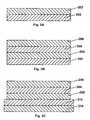
- Figures 1A to 1Dare schematic sections through a sub-assembly and front plane laminate formed by a first PFCA process.
- the processbegins by coating a layer of electro-optic medium 102 on a first release sheet 100 (deposition techniques other than coating may be useful depending upon the exact type of electro-optic medium used).
- a layer of lamination adhesive 104is coated on a second release sheet 106 and the resultant sub-assembly laminated to the electro-optic medium layer 102 on the first release sheet 100 so that the lamination adhesive layer 104 is secured to the electro-optic medium layer 102, to produce the sub-assembly shown in Figure 1B .
- Electrode layer 110is laminated to the adhesive layer 104 so that the electrode layer 110 extends across the aperture 108, as illustrated in Figure 1D .
- the electrode layer 110would normally be supported on a support sheet, but the support sheet is omitted from Figure 1D for simplicity.
- the electrode layer 110is shown as larger than the adhesive layer 104 and the electro-optic medium layer 104. This is deliberate, since the final front plane laminate shown in Figure 1D is intended for use in the production of an electro-optic display with a so-called "underfill" edge seal, as described in the aforementioned WO 2003/104884 .
- the backplane, the electrode layer and the front support layerare all made larger in both dimensions than the intervening adhesive and electro-optic medium layers, so that after the front plane laminate has been laminated to the backplane a sealing material can be injected between the backplane and the electrode or front support and cured to form an edge seal completely surrounding the adhesive and electro-optic medium layers.
- aperture 108could extend to the periphery of the electro-optic medium layer 102 and the adhesive layer 104 so as to form a cut-out in the edge of these layers rather than a true aperture. It is not strictly necessary to coat the adhesive layer 104 on a second release sheet; depending upon the specific adhesive and electro-optic medium employed, it may be possible to coat the adhesive layer directly on to the electro-optic medium layer.
- FIG. 1A to 1Dalso allows considerable flexibility as to which operations are performed on continuous webs of material and which are performed on cut pieces of material sized for individual displays (or possibly sized for a small number of displays produced in a single lamination operation).
- the steps illustrated in Figures 1A and 1Bwould normally be carried out on continuous webs of material.
- the formation of the aperture 108might be done either on a continuous web or on cut pieces of material.
- the final lamination to the "oversized" electrode layer 110would normally be effected on cut pieces of material.
- the processdoes not provide the adhesive layer typically present between the electro-optic medium layer 102 and its associated release sheet 100.
- the final front plane laminatemay be used in a process in which a lamination adhesive is placed on the backplane, or in which no lamination adhesive is needed because, for example, the electro-optic medium is an encapsulated electrophoretic medium in which the capsules are embedded in a polymeric binder which can itself serve as a lamination adhesive, as described in certain of the aforementioned E Ink patents and applications.
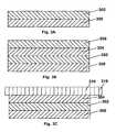
- Figures 2A to 2Eillustrate a second preferred PFCA process.
- the first two steps of this process, illustrated in Figures 2A and 2B , and carried out using a first release sheet 200, an electro-optic medium layer 202, an adhesive layer 204 and a second release sheet 206,are identical to the corresponding steps illustrated in Figures 1A and 1B .
- the next step of the second preferred PFCA processcomprises removing the first release sheet 200 and laminating to the thus-exposed surface of the electro-optic medium layer 202 a second lamination adhesive layer 212 carried on a third release sheet 214, as illustrated in Figure 2C .
- the remaining steps of the processare the formation of an aperture 208 through all five layers of the structure shown in Figure 2C , to produce the apertured structure shown in Figure 2D , and the removal of the second release sheet 206 and lamination of an electrode layer 210, which extends across the aperture 208, to produce the finished front plane laminate shown in Figure 2E .
- both the second lamination adhesive layer 212 and the electrode layer 210are made larger than the intervening electro-optic medium layer 202 and the adhesive layer 204; although not apparent from Figure 2E , this difference in size exists in both dimensions, and is provided so that, during the final lamination to produce the front plane laminate shown in Figure 2E , the peripheral portions of the second lamination adhesive layer 212 will bond to the electrode layer, thus forming an edge seal around the electro-optic medium layer 202 (the thicknesses of the layers in Figures 2A to 2E are of course greatly exaggerated relative to their lateral dimensions).
- the first two steps(to produce the structure shown in Figure 2B ) will typically be carried out on continuous webs of material and the remaining steps on pieces of material cut to size for individual displays.
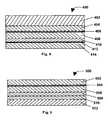
- Figures 3A to 3Eillustrate a preferred extended tab process.
- the first two steps of this process, illustrated in Figures 3A and 3B , and carried out using a first release sheet 300, an electro-optic medium layer 302, an adhesive layer 304 and a second release sheet 306,are identical to the corresponding steps illustrated in Figures 1A and 1B .
- the next step of the processnamely removal of the second release sheet 306 and lamination of an electrode layer 310, is also generally similar to the first PFCA process, but no aperture is formed and, as illustrated in Figures 3C and 3E , the electrode layer 310 is slightly larger in both dimensions than the electro-optic medium layer 302, and is also provided with a projecting tab 316 which will eventually be used to connect the electrode layer 310 to a backplane.
- the last step of the extended tab processis generally similar to that the second PFCA process described above; the first release sheet 300 is removed and the thus-exposed surface of the electro-optic medium layer 302 is laminated to a second lamination adhesive layer 312 carried on a third release sheet 314, as illustrated in Figure 3D .
- the relative sizes of the various layers of the final front plane laminateare designed to ensure that during the final lamination, the second adhesive layer 312 becomes bonded to the electrode layer 310, thus forming an edge seal around the electro-optic medium layer 302.
- the "aperture”may be either a true aperture or a cut-out from an edge of the electro-optic medium and adhesive layers, while the extended tab process does not require the formation of any aperture.
- Locating an aperture in the interior of the electro-optic medium and adhesive layersi.e., using a PFCA process with a true aperture rather than a cut-out) allows for a compact design, but does not allow the entire active area of the electro-optic medium to be used for the display, since it is necessary to hide the connection area.
- the strain on the front electrodeis low and there is no risk of compromising the edge of the display since the connection area is spaced from the edge seal.
- PFCA processwith a cut-out can improve the use of the active area of the electro-optic medium while keeping the strain on the connection low.
- Use of an external tab processallows the entire active area of the electro-optic medium to be used, but does require additional space on the backplane to accommodate the external tab.
- the strain on the external tab connectionmay be greater than in a PFCA process, but there is little or no risk of compromising the edge seal of the display. In all cases, the use of multiple connections may be desirable to minimize the possibility of display failure due to poor electrical connections or strain on such connections.
- the PFCA and extended tab displaysmay include various additional layers to enhance the protection of the electro-optic medium from materials, especially moisture, present in the environment.
- one preferred form of front substrate for electro-optic displayscomprises a thin layer of ITO on poly(ethylene terephthalate) (PET), such coated films being readily available commercially.
- PETpoly(ethylene terephthalate)
- the ITO layerserves as a barrier material, but in practice inevitably suffers from pinholes and cracks, through which moisture and other contaminants can penetrate to the electro-optic medium.
- a redundant barrier layeron to the front substrate, this redundant barrier layer being formed of a homopolymer (for example, polychlorotrifluoroethylene, available from Honeywell Corporation under the Registered Trade Mark “ACLAR"), or a sputtered ceramic (for example AlO x , available from Toppan Printing Company of under the trade name Toppan GX Film).
- a homopolymerfor example, polychlorotrifluoroethylene, available from Honeywell Corporation under the Registered Trade Mark "ACLAR”
- a sputtered ceramicfor example AlO x , available from Toppan Printing Company of under the trade name Toppan GX Film.
- the redundant barrier layershould be thin, ideally about 12 ⁇ m, but could be as thick as 5 mil (127 ⁇ m) if sufficient flexibility is still available.
- the adhesive layershould be transparent, colorless, thin, flexible, have low creep (when the display is flexed or rolled), and be durable at all temperatures within the operating range of the display.
- Certain cross-linked polyurethanes and polyacrylatescan be used as such adhesives.
- the barrier properties of a PET/ITO or similar front substratemay be improved by coating a redundant metal oxide layer (for example, an alumina layer) either on the opposed surface of the front substrate from the ITO layer or underneath the ITO layer.
- a redundant metal oxide layerfor example, an alumina layer
- the combination of the ITO layer and the redundant metal oxide layerimproves the barrier properties of the front substrate (for example by reducing migration of water vapor through the inevitable cracks and pinholes in the ITO layer) without undue yellowing of the substrate, such as would occur one attempted to improve barrier properties by increasing the thickness of the ITO layer.
- a more complex structure containing a ceramic materialsuch as Barix (Registered Trade Mark) sealing material, available from Vitex Systems, Inc., 3047 Orchard Parkway, San Jose, CA 95134 could be used; again the barrier layer could be provided on the surface of the front substrate remote from the ITO layer or beneath the ITO layer.
- Vitex Systemscurrently sells a polymer film bearing both Barix and ITO layers under the trade name FlexGlass 200, but the polymeric film is 5 mil (127 ⁇ m) PEN.
- the barrier properties of the front substratemay also be controlled by careful choice of both the polymer and conductive material used in the front substrate.
- suitable polymersinclude PET, PEN, polycarbonate, poly(vinylidene chloride) (sold under the Registered Trade Mark “SARAN”), polychlorotrifluoroethylene (sold under the Registered Trade Marks “ACLAR” and “CLARIS”), triacetyl cellulose, the material sold under the Registered Trade Mark “ARTON” by JSR Company, polyethersulfone (PES) and laminates of two or more of these materials.
- Suitable transparent conductive materialsinclude ITO, organic conductive polymers such as Baytron P (Registered Trade Mark), carbon nanotubes, and other suitably conducting light transmissive conductors (T > 60 per cent) having resistivities of less an about 10 4 ohms/square.
- the electro-optic layermay be an encapsulated electrophoretic layer, a polymer-dispersed electrophoretic layer, or any of the other types of electro-optic layer discussed above.
- the displaymay contain one or two lamination adhesive layers to attach the electro-optic material to the front substrate and/or the backplane.
- the displaymay be viewed through either lamination adhesive layer, and the display may be assembled by direct coating and lamination, or by the use of front plane laminates, inverted front plane laminates, or double release films, as described in the applications mentioned in the first paragraph of this application.
- the displayis normally viewed through the front substrate, in some cases a light-transmissive backplane can be used to provide a double-sided display, or one operating in the aforementioned shutter mode.
- the displaymay be provided with any of the types of edge seal described in the aforementioned PCT/US2006/62399 , or those described below.
- Section BStiffened front plane laminates and processes
- another aspectprovides a modification of the process for forming an electro-optic display using a front plane laminate as described in the aforementioned WO 2003/104884 .
- the processis modified by securing a stiffening layer to at least one of the front plane laminate and the backplane before the front plane laminate is laminated to the backplane to form the electro-optic display. After the lamination, the stiffening layer will typically be removed.
- the stiffening layermay be secured to the front plane laminated prior to the lamination to the backplane, we do not exclude the possibility that the FPL may be manufactured with the stiffening layer in place, and indeed this may often be the most convenient approach, since the stiffening effect provided by the stiffening layer may be useful during the manufacture of the FPL itself, as well as during its lamination to the backplane.
- a stiffening layerit may be advantageous to first secure the substrate to a stiffening layer, then prepare the FPL by coating the electro-optic medium, followed by the adhesive layer, on to the substrate, and finally covering the adhesive with a release sheet.
- stiffness of the substrate provided by the stiffening layermay provide beneficial improvements in tensioning and uniformity if (as is normally the case), the coating processes are carried out on a web.
- the resultant FPLmay then be laminated to a backplane in the usual manner to form an electro-optic display, and the stiffening layer removed from the final display.
- FIG. 4is a schematic cross-section through a stiffened front plane laminate (generally designated 400).
- the front plane laminate 400comprises a stiffening layer 402, a polymeric support layer 404, a light-transmissive electrically-conductive layer 406, an electro-optic medium layer 408, a lamination adhesive layer 410, and a release sheet 414 provided, on its surface facing the lamination adhesive layer, with a conductive layer 412; this conductive layer 412 is used, as described in the aforementioned U.S. Patent 6,982,178 and as briefly described above, for testing the electro-optic medium prior to incorporation of the FPL into a display.
- the electro-optic medium and adhesive layerscan be of any of the types described in the aforementioned WO 2003/104884 ; WO 2004/023195 ; WO 2005/041160 ; WO 2005/073777 ; PCT/US2006/60049 and PCT/US2006/62399 .
- the electro-optic mediummay be an encapsulated electrophoretic medium, a polymer-dispersed electrophoretic medium, a rotating bichromal member medium, a microcell electrophoretic medium or any of the other types of electro-optic medium discussed above.
- the FPLmay be of the conventional type described in WO 2003/104884 , with the adhesive layer adjacent the release sheet, or of the inverted type described in the aforementioned PCT/US2006/60049 , in which the order of the electro-optic medium layer and the adhesive layer is reversed, so that the electro-optic medium layer lies closer to the release sheet.
- the "FPL”may also have the form of a double release sheet comprising a single layer of electro-optic medium sandwiched between two separate adhesive layers.
- the stiffening layercan be made from a wide variety of materials.
- the stiffening layerwill be a polymeric film, and may be formed from, for example, polyethylene, polypropylene, poly(ethylene terephthalate) or other polymers.
- the stiffening layermay be secured to the front plane laminate or the backplane by a releasable adhesive, or by static cling.
- a typical assembly sequence for an electro-optic display using a stiffened front plane laminatewould be to remove the release sheet and laminate the FPL to a backplane (which may or may not be stiffened with an additional stiffening layer). If a edge sealing material is to be dispensed around the periphery of the display and cured to form an edge seal, this is normally done as the next stage of the process. Finally, the stiffening layer(s) are removed.
- a stiffening layercan also be used at other stages in the assembly of electro-optic displays to aid in the processing of thin layers. For example, if a composite front substrate of an electro-optic display is to be assembled from individual layers (such as a 0.5 mil (13 ⁇ m) ITO/PET film and a 0.5 mil (13 ⁇ m) AlO x /PET film), a stiffening layer can be applied to one of the films to allow a bonding adhesive to be coated prior to laminating the two layers together. Such a stiffening layer may be left in place to aid in downstream processing.
- the electro-optic displays produced using stiffening filmsmay incorporate any of the known types of additional sealing layers or edge seals to isolate the electro-optic medium from the environment, as discussed in Section A above.
- Section CDouble adhesive layer displays and front plane laminates
- the aforementioned compromiseis avoided by using a double layer of adhesive, with a non-cross-linked adhesive layer adjacent the backplane to provide good backplane conformity, i.e., the soft adhesive provides the flow properties needed for good bonding with relatively rough backplanes, and a cross-linked adhesive layer adjacent the electro-optic medium; this cross-linked adhesive layer prevents void growth by preventing out-gassing of volatile components from the electro-optic layer.
- the cross-linked adhesivemay also serve as a moisture barrier to maintain a constant moisture level within the electro-optic medium; this can be important, since the electro-optic performance of many types of electro-optic media varies with the moisture content of the media.
- each of the adhesive layersmay have a thickness of about 25 ⁇ m.
- FIG. 5 of the accompanying drawingsis a schematic cross-section through a double adhesive layer electro-optic display (generally designated 500) of the present invention.
- the display 500comprises a front substrate 502, a light-transmissive electrode layer 504, an electro-optic layer 506, a cross-linked adhesive layer 508 (which may be formed, for example, from a polyurethane adhesive cross-linked with diglycidylaniline), a non-cross-linked adhesive layer 510 (which may be formed from a non-cross-linked polyurethane), and a backplane 512 provided with pixel electrodes (not shown).
- the display 500can readily be formed using a double adhesive layer front plane laminate of the present invention; such a DALFPL can be similar to the FPL 400 shown in Figure 4 except that the single adhesive layer of the FPL 400 would be replaced by the double adhesive layer 508, 510 shown in Figure 5 .
- experimental single-pixel displayswere prepared. These displays were substantially as shown in Figure 5 except that the backplane comprised a single gold electrode placed upon an insulating backplane larger than the gold electrode so as to leave a peripheral portion of the insulating backplane exposed all around the gold electrode.
- a protective sheetwas provided covering the exposed surface of the front substrate and having a peripheral portion extending outwardly beyond the edges of the front substrate.
- a sealing materialwas injected between the peripheral portions of the backplane and the protective sheet to form a edge seal, thus forming a sealed display generally similar to that shown in Figure 20 of the aforementioned WO 2003/104884 .
- the electro-optic medium used in the displayswas an encapsulated electrophoretic medium comprising an internal phase of polymer-coated titania and polymer-coated carbon black in a hydrocarbon fluid, encapsulated within gelatin/acacia capsules and prepared substantially as described at page 20, line 17 to page 22, lines 17 of the aforementioned WO 02/079869 .
- the double adhesive layer usedcomprised 25 ⁇ m layers of cross-linked and non-cross-linked custom polyurethane adhesive; control displays were prepared with a single 50 ⁇ m layer of the same non-cross-linked adhesive.
- Both the test and control displayswere stored and 75°C and in a dry atmosphere, and their switching abilities tested at intervals.
- the double adhesive layer displays of the present inventionshowed no void growth after 664 hours at 75°C, while the control displays using a single adhesive layer developed voids in less than 24 hours.
- the displays of the present inventionalso failed to show voids at 348 hours at 60°C and 80 per cent relative humidity, and 348 hours at 40°C and 90 per cent relative humidity; in each case, the control displays showed void growth after much shorter periods of storage.
- the double adhesive layer electro-optic displays of the present inventionmay incorporate any of the known types of additional sealing layers or edge seals to isolate the electro-optic medium from the environment, as discussed in Section A above.
- Section DForming electro-optic displays without front plane laminates
- Assembling complex electro-optic displays with integrated barrier layers and/or edge sealscan be a complicated process. It is possible to deliver to a manufacturer a front plane laminate containing all required layers of the final display, but forming this front plane laminate may require alignment of various layers during several lamination steps. Depending upon the alignment tolerances required, it may not be possible to form the FPL using web or sheet based processes. Typically, the edge seals will still need to be formed individually for each display by the manufacturer. It may also be desirable for manufacturing and inventory reasons to avoid assembling an entire FPL structure before delivery to the manufacturer of the final display.
- an electro-optic display layer-by-layerrather than by providing an integrated FPL.
- Such a layer-by-layer approachmay also have manufacturing advantages by allowing each layer to be separately coated, converted and inspected in such a manner as is required to achieve cost efficiency for that layer alone.
- the approachalso allows flexibility in delivering different layers to different manufacturers of displays with the layers custom tailored to their individual needs without requiring the manufacture of a fully assembled FPL for each manufacturer.
- the electro-optic display 600(which is identical to that shown in Figure 9 of the aforementioned PCT/US2006/62399 ), comprises a front substrate 602, having barrier properties and bearing on its lower surface (as illustrated in Figure 6E ) a thin, transparent electrically-conductive layer (not shown separately in Figure 6E ).
- the display 600further comprises an upper lamination adhesive layer 604, an electro-optic layer 606, a lower lamination adhesive layer 608, and a backplane 610, which has barrier properties similar to those of the front substrate 602.
- the front substrate 602 and the backplane 610are both made larger in both dimensions than the intervening layers 604, 606 and 608 so that peripheral portions 602P and 610P of the front substrate 602 and the backplane 610 respectively extend outwardly beyond the edges of these intervening layers.
- An edge seal 612extends between the peripheral portions 602P and 610P, thus forming a complete seal around the electro-optic layer 606.
- FIGS 6A to 6Dillustrate successive stages in the manufacture of the electro-optic display 600.
- One preferred process for forming the electro-optic displaybegins with a web of the lower lamination adhesive layer 608 sandwiched between first and second release sheets; such a web can of course be prepared by coating the adhesive layer on one release sheet and covering the coated layer with the other release sheet.
- a piece of the size required to provide the lower lamination adhesive layer 608 shown in Figure 6Eis cut from the web, the first release sheet is removed, and the adhesive layer 608 and the second release sheet 614 are laminated to the backplane 610 to form the structure shown in Figure 6A .
- a web of the electro-optic layer 606is formed sandwiched between third and fourth release sheets; such a web can of course be prepared by coating the electro-optic layer on one release sheet and covering the coated layer with the other release sheet.
- a piece of the size required to provide the electro-optic layer 606 shown in Figure 6Eis cut from the web, and the third release sheet is removed.
- the second release sheet 614is removed from the structure shown in Figure 6A .
- the electro-optic layer/fourth release sheetis then laminated to the lower adhesive layer to produce the structure shown in Figure 6B , in which the electro-optic layer 606 is covered by the fourth release sheet 616.
- the third stage of the processis closely analogous to the first.
- a web of the upper lamination adhesive layer 604 sandwiched between fifth and sixth release sheetsis prepared, and a piece of the size required to provide the upper lamination adhesive layer 604 shown in Figure 6E is cut from the web.
- the fifth release sheetis removed, the fourth release sheet is removed from the structure shown in Figure 6B , and the upper adhesive layer 604 is laminated to the electro-optic layer 606 to produce the structure shown in Figure 6C , in which the adhesive layer 604 is covered by the sixth release sheet 618.
- a web of the front substrate 602is secured to a web of a stiffening layer 620, the resultant composite web is cut to produce a piece with the size required for front substrate 602 in Figure 6E , the sixth release sheet 618 is removed from the structure shown in Figure 6C , and the front substrate 602 is laminated to adhesive layer 604 to produce the structure shown in Figure 6D .
- the material required to form the edge seal 612can be dispensed between the peripheral portions 602P and 610P, and cured to form the edge seal 612 shown the Figure 6E .
- the stiffening layer 620can then be removed to form the final electro-optic display 600.
- each layeris added separately to the stack of layers formed on the backplane 610.
- the lower adhesive layer 608, the electro-optic layer 606 and the upper adhesive layer 604could all be prepared in the form of webs as already described, the separate webs laminated together after removing one release sheet from each web, and pieces only cut to size after all three layers had been laminated together.
- the two release sheetsneed to have asymmetric characteristics, i.e., different degrees of adhesion to the central layer, so that one of the release sheets can be removed without disturbing the other.
- asymmetric characteristicsi.e., different degrees of adhesion to the central layer
- the displays of the present inventionmay incorporate any known type of edge seal, including any of the types of edge seal described in the aforementioned PCT/US2006/62399 .
- the displays of the present inventionmay also incorporate any of the known types of additional sealing layers to isolate the electro-optic medium from the environment, as discussed in Section A above.
- the processes described aboveallow electro-optic displays to be manufactured using laminations with tight tolerances, as required for many active matrix applications.
- the processesmay also, in some cases, facilitate the formation of edge seals.
- the electrode arrangements in the displays of all aspects of the present inventioncan be of any of the types described in the aforementioned E Ink and MIT patents and applications.
- the displaysmay be of the direct drive type, in which the backplane is provided with a plurality of electrodes, each of which is provided with a separate connector by means of a which a controller can control the voltage applied to the specific electrode.
- a single continuous front electrodeis usually provided covering the whole display, although other front electrode arrangements are possible.
- the backplanecarries a plurality of elongate parallel electrodes ("column electrodes”), while on the opposed side of the electro-optic material there is provided a plurality of elongate parallel electrodes (“row electrodes”) running at right angles to the column electrodes, the overlap between one specific column electrode and one specific row electrode defining one pixel of the display.
- the present displaysmay also be of the active matrix type, typically with a single continuous front electrode covering the whole display and a matrix of pixel electrodes on the backplane, each pixel electrode defining one pixel of the display and having an associated transistor or other non-linear element, the active matrix display being scanned in the conventional manner to write the display in a row-by-row fashion.
- the present displaymay also be of the stylus-driven type. with (typically) a single electrode on the backplane and no permanent front electrode, writing of the display being effected by moving a stylus across the front surface of the display.
Landscapes
- Physics & Mathematics (AREA)
- Nonlinear Science (AREA)
- Optics & Photonics (AREA)
- General Physics & Mathematics (AREA)
- Electrochemistry (AREA)
- Molecular Biology (AREA)
- Health & Medical Sciences (AREA)
- Chemical Kinetics & Catalysis (AREA)
- Chemical & Material Sciences (AREA)
- Life Sciences & Earth Sciences (AREA)
- Electrochromic Elements, Electrophoresis, Or Variable Reflection Or Absorption Elements (AREA)
- Optical Modulation, Optical Deflection, Nonlinear Optics, Optical Demodulation, Optical Logic Elements (AREA)
- Laminated Bodies (AREA)
- Devices For Indicating Variable Information By Combining Individual Elements (AREA)
- Apparatuses And Processes For Manufacturing Resistors (AREA)
- Electroluminescent Light Sources (AREA)
Abstract
Description
- This invention is related to International Applications Publication Nos.
WO 2003/104884 ;WO 2004/023195 ;WO 2005/041160 ; andWO 2005/073777 ; and International Applications Nos.PCT/US2006/60049 andPCT/US2006/62399 . The reader is referred to these International Applications for background information relating to this invention. - This invention relates to methods for the production of electro-optic displays, to components for use in such methods and to displays produced using such methods and components. This invention is particularly, but not exclusively, intended for use with displays comprising encapsulated electrophoretic media. However, the invention can also make use of various other types of electro-optic media which are solid, in the sense that they have solid external surfaces, although the media may, and often do, have internal cavities which contain a fluid (either liquid or gas). Thus, the term "solid electro-optic displays" includes encapsulated electrophoretic displays, encapsulated liquid crystal displays, and other types of displays discussed below.
- Electro-optic displays comprise a layer of electro-optic material, a term which is used herein in its conventional meaning in the imaging art to refer to a material having first and second display states differing in at least one optical property, the material being changed from its first to its second display state by application of an electric field to the material. Although the optical property is typically color perceptible to the human eye, it may be another optical property, such as optical transmission, reflectance, luminescence or, in the case of displays intended for machine reading, pseudo-color in the sense of a change in reflectance of electromagnetic wavelengths outside the visible range.
- The terms "bistable" and "bistability" are used herein in their conventional meaning in the art to refer to displays comprising display elements having first and second display states differing in at least one optical property, and such that after any given element has been driven, by means of an addressing pulse of finite duration, to assume either its first or second display state, after the addressing pulse has terminated, that state will persist for at least several times, for example at least four times, the minimum duration of the addressing pulse required to change the state of the display element. It is shown in International Application Publication No.
WO 02/079869 - Several types of electro-optic displays are known. One type of electro-optic display is a rotating bichromal member type as described, for example, in
U.S. Patents Nos. 5,808,783 ;5,777,782 ;5,760,761 ;6,054,071 6,055,091 ;6,097,531 ;6,128,124 ;6,137,467 ; and6,147,791 (although this type of display is often referred to as a "rotating bichromal ball" display, the term "rotating bichromal member" is preferred as more accurate since in some of the patents mentioned above the rotating members are not spherical). Such a display uses a large number of small bodies (typically spherical or cylindrical) which have two or more sections with differing optical characteristics, and an internal dipole. These bodies are suspended within liquid-filled vacuoles within a matrix, the vacuoles being filled with liquid so that the bodies are free to rotate. The appearance of the display is changed by applying an electric field thereto, thus rotating the bodies to various positions and varying which of the sections of the bodies is seen through a viewing surface. This type of electro-optic medium is typically bistable. - Another type of electro-optic display uses an electrochromic medium, for example an electrochromic medium in the form of a nanochromic film comprising an electrode formed at least in part from a semi-conducting metal oxide and a plurality of dye molecules capable of reversible color change attached to the electrode; see, for exampleO'Regan, B., et al., Nature 1991, 353, 737; andWood, D., Information Display, 18(3), 24 (March 2002). See alsoBach, U., et al., Adv. Mater., 2002, 14(11), 845. Nanochromic films of this type are also described, for example, in
U.S. Patents Nos. 6,301,038 ;6,870.657 ; and6,950,220 . This type of medium is also typically bistable. - Another type of electro-optic display is an electro-wetting display developed by Philips and described inHayes, R.A., et al., "Video-Speed Electronic Paper Based on Electrowetting", Nature, 425, 383-385 (2003). It is shown in International Application Publication No.
WO 2005/038764 that such electro-wetting displays can be made bistable. - Another type of electro-optic display, which has been the subject of intense research and development for a number of years, is the particle-based electrophoretic display, in which a plurality of charged particles move through a fluid under the influence of an electric field. Electrophoretic displays can have attributes of good brightness and contrast, wide viewing angles, state bistability, and low power consumption when compared with liquid crystal displays. Nevertheless, problems with the long-term image quality of these displays have prevented their widespread usage. For example, particles that make up electrophoretic displays tend to settle, resulting in inadequate service-life for these displays.
- As noted above, electrophoretic media require the presence of a fluid. In most prior art electrophoretic media, this fluid is a liquid, but electrophoretic media can be produced using gaseous fluids; see, for example,Kitamura, T., et al., "Electrical toner movement for electronic paper-like display", IDW Japan, 2001, Paper HCS1-1, andYamaguchi, Y., et al., "Toner display using insulative particles charged triboelectrically", IDW Japan, 2001, Paper AMD4-4). See also
U.S. Patent Publication No. 2005/0001810 ; European Patent Applications1,462,847 ;1,482,354 ;1,484,635 ;1,500,971 ;1,501,194 ;1,536,271 ;1,542,067 ;1,577,702 ;1,577,703 ; and1,598,694 ; and International Applications Publication Nos.WO 2004/090626 ;WO 2004/079442 ; andWO 2004/001498 . Such gas-based electrophoretic media appear to be susceptible to the same types of problems due to particle settling as liquid-based electrophoretic media, when the media are used in an orientation which permits such settling, for example in a sign where the medium is disposed in a vertical plane. Indeed, particle settling appears to be a more serious problem in gas-based electrophoretic media than in liquid-based ones, since the lower viscosity of gaseous suspending fluids as compared with liquid ones allows more rapid settling of the electrophoretic particles. - Numerous patents and applications assigned to or in the names of the Massachusetts Institute of Technology (MIT) and E Ink Corporation have recently been published describing encapsulated electrophoretic media. Such encapsulated media comprise numerous small capsules, each of which itself comprises an internal phase containing electrophoretically-mobile particles suspended in a liquid suspending medium, and a capsule wall surrounding the internal phase. Typically, the capsules are themselves held within a polymeric binder to form a coherent layer positioned between two electrodes. Encapsulated media of this type are described, for example, in
U.S. Patents Nos. 5,930,026 ;5,961,804 ;6,017,584 ;6,067,185 ;6,118,426 ;6,120,588 ;6,120,839 ;6,124,851 ;6,130,773 ;6,130,774 ;6,172,798 ;6,177,921 ;6,232,950 ;6,249,271 ;6,252,564 ;6,262,706 ;6,262,833 ;6,300,932 ;6,312,304 ;6,312,971 ;6,323,989 ;6,327,072 ;6,376,828 ;6,377,387 ;6,392,785 ;6,392,786 ;6,413,790 ;6,422,687 ;6,445,374 ;6,445,489 ;6,459,418 ;6,473,072 ;6,480,182 ;6,498,114 ;6,504,524 ;6,506,438 ;6,512,354 ;6,515,649 ;6,518,949 ;6,521,489 ;6,531,997 ;6,535,197 ;6,538,801 ;6,545,291 ;6,580,545 ;6,639,578 ;6,652,075 ;6,657,772 ;6,664,944 ;6,680,725 ;6,683,333 ;6,704,133 ;6,710,540 ;6,721,083 ;6,724,519 ;6,727,881 ;6,738,050 ;6,750,473 ;6,753,999 ;6,816,147 ;6,819,471 ;6,822,782 ;6,825,068 ;6,825,829 ;6,825,970 ;6,831,769 ;6,839,158 ;6,842,167 ;6,842,279 ;6,842,657 ;6,864,875 ;6,865,010 ;6,866,760 ;6,870,661 ;6,900,851 ;6,922,276 ;6,950,200 ;6,958,848 ;6,967,640 ;6,982,178 ;6,987,603 ;6,995,550 ;7,002,728 ;7,012,600 ;7,012,735 ;7,023,420 ;7,030,412 ;7,030,854 ;7,034,783 ;7,038,655 ;7,061,663 ;7,071,913 ;7,075,502 ;7,075,703 ;7,079,305 ;7,106,296 ;7,109,968 ;7,110,163 ;7,110,164 ;7,116,318 ;7,116,466 ;7,119,759 ;7,119,772 ;7,148,128 ;7,167,155 ;7,170,670 ; and7,173,752 ; andU.S. Patent Applications Publication Nos. 2002/0060321 ;2002/0090980 ;2003/0011560 ;2003/0102858 ;2003/0151702 ;2003/0222315 ;2004/0014265 ;2004/0075634 ;2004/0094422 ;2004/0105036 ;2004/0112750 ;2004/0119681 ;2004/0136048 ;2004/0155857 ;2004/0180476 ;2004/0190114 ;2004/0196215 ;2004/0226820 ;2004/0239614 ;2004/0257635 ;2004/0263947 ;2005/0000813 ;2005/0007336 ;2005/0012980 ;2005/0017944 ;2005/0018273 ;2005/0024353 ;2005/0062714 ;2005/0067656 ;2005/0078099 ;2005/0099672 ;2005/0122284 ;2005/0122306 ;2005/0122563 ;2005/0134554 ;2005/0146774 ;2005/0151709 ;2005/0152018 ;2005/0152022 ;2005/0156340 ;2005/0168799 ;2005/0179642 ;2005/0190137 ;2005/0212747 ;2005/0213191 ;2005/0219184 ;2005/0253777 ;2005/0270261 ;2005/0280626 ;2006/0007527 ;2006/0024437 ;2006/0038772 ;2006/0139308 ;2006/01393 10 ;2006/0139311 ;2006/0176267 ;2006/0181492 ;2006/0181504 ;2006/0194619 ;2006/0197736 ;2006/0197737 ;2006/0197738 ;2006/0198014 ;2006/0202949 ; and2006/0209388 ; and International Applications Publication Nos.WO 00/38000 WO 00/36560 WO 00/67110 WO 01/07961 1,099,207 B1 ; and1,145,072 B1 . - Many of the aforementioned patents and applications recognize that the walls surrounding the discrete microcapsules in an encapsulated electrophoretic medium could be replaced by a continuous phase, thus producing a so-called polymer-dispersed electrophoretic display, in which the electrophoretic medium comprises a plurality of discrete droplets of an electrophoretic fluid and a continuous phase of a polymeric material, and that the discrete droplets of electrophoretic fluid within such a polymer-dispersed electrophoretic display may be regarded as capsules or microcapsules even though no discrete capsule membrane is associated with each individual droplet; see for example, the aforementioned
U.S. Patent No. 6,866,760 . Accordingly, for purposes of the present application, such polymer-dispersed electrophoretic media are regarded as sub-species of encapsulated electrophoretic media. - A related type of electrophoretic display is a so-called "microcell electrophoretic display". In a microcell electrophoretic display, the charged particles and the fluid are not encapsulated within microcapsules but instead are retained within a plurality of cavities formed within a carrier medium, typically a polymeric film. See, for example,
U.S. Patents Nos. 6,672,921 and6,788,449 , both assigned to Sipix Imaging, Inc. - Although electrophoretic media are often opaque (since, for example, in many electrophoretic media, the particles substantially block transmission of visible light through the display) and operate in a reflective mode, many electrophoretic displays can be made to operate in a so-called "shutter mode" in which one display state is substantially opaque and one is light-transmissive. See, for example, the aforementioned
U.S. Patents Nos. 6,130,774 and6,172,798 , andU.S. Patents Nos. 5,872,552 ;6,144,361 ;6,271,823 ;6,225,971 ; and6,184,856 . Dielectrophoretic displays, which are similar to electrophoretic displays but rely upon variations in electric field strength, can operate in a similar mode; seeU.S. Patent No. 4,418,346 . - An encapsulated or microcell electrophoretic display typically does not suffer from the clustering and settling failure mode of traditional electrophoretic devices and provides further advantages, such as the ability to print or coat the display on a wide variety of flexible and rigid substrates. (Use of the word "printing" is intended to include all forms of printing and coating, including, but without limitation: pre-metered coatings such as patch die coating, slot or extrusion coating, slide or cascade coating, curtain coating; roll coating such as knife over roll coating, forward and reverse roll coating; gravure coating; dip coating; spray coating; meniscus coating; spin coating; brush coating; air knife coating; silk screen printing processes; electrostatic printing processes; thermal printing processes; ink jet printing processes; electrophoretic deposition; and other similar techniques.) Thus, the resulting display can be flexible. Further, because the display medium can be printed (using a variety of methods), the display itself can be made inexpensively.
- Other types of electro-optic materials may also be used in the present invention.
- An electro-optic display normally comprises a layer of electro-optic material and at least two other layers disposed on opposed sides of the electro-optic material, one of these two layers being an electrode layer. In most such displays both the layers are electrode layers, and one or both of the electrode layers are patterned to define the pixels of the display. For example, one electrode layer may be patterned into elongate row electrodes and the other into elongate column electrodes running at right angles to the row electrodes, the pixels being defined by the intersections of the row and column electrodes. Alternatively, and more commonly, one electrode layer has the form of a single continuous electrode and the other electrode layer is patterned into a matrix of pixel electrodes, each of which defines one pixel of the display. In another type of electro-optic display, which is intended for use with a stylus, print head or similar movable electrode separate from the display, only one of the layers adjacent the electro-optic layer comprises an electrode, the layer on the opposed side of the electro-optic layer typically being a protective layer intended to prevent the movable electrode damaging the electro-optic layer.
- The manufacture of a three-layer electro-optic display normally involves at least one lamination operation. For example, in several of the aforementioned MIT and E Ink patents and applications, there is described a process for manufacturing an encapsulated electrophoretic display in which an encapsulated electrophoretic medium comprising capsules in a binder is coated on to a flexible substrate comprising indium tin oxide (ITO) or a similar conductive coating (which acts as an one electrode of the final display) on a plastic film, the capsules/binder coating being dried to form a coherent layer of the electrophoretic medium firmly adhered to the substrate. Separately, a backplane, containing an array of pixel electrodes and an appropriate arrangement of conductors to connect the pixel electrodes to drive circuitry, is prepared. To form the final display, the substrate having the capsule/binder layer thereon is laminated to the backplane using a lamination adhesive. (A very similar process can be used to prepare an electrophoretic display usable with a stylus or similar movable electrode by replacing the backplane with a simple protective layer, such as a plastic film, over which the stylus or other movable electrode can slide.) In one preferred form of such a process, the backplane is itself flexible and is prepared by printing the pixel electrodes and conductors on a plastic film or other flexible substrate. The obvious lamination technique for mass production of displays by this process is roll lamination using a lamination adhesive. Similar manufacturing techniques can be used with other types of electro-optic displays. For example, a microcell electrophoretic medium or a rotating bichromal member medium may be laminated to a backplane in substantially the same manner as an encapsulated electrophoretic medium.
- In the processes described above, the lamination of the substrate carrying the electro-optic layer to the backplane may advantageously be carried out by vacuum lamination. Vacuum lamination is effective in expelling air from between the two materials being laminated, thus avoiding unwanted air bubbles in the final display; such air bubbles may introduce undesirable artifacts in the images produced on the display. However, vacuum lamination of the two parts of an electro-optic display in this manner imposes stringent requirements upon the lamination adhesive used, as described in the aforementioned
U.S. Patent Nos. 6,657,772 and6,831,769 , especially in the case of a display using an encapsulated electrophoretic medium. The lamination adhesive must have sufficient adhesive strength to bind the electro-optic layer to the layer (typically an electrode layer) to which it is to be laminated, and in the case of an encapsulated electrophoretic medium, the adhesive must also have sufficient adhesive strength to mechanically hold the capsules together. If the electro-optic display is to be of a flexible type (and one of the important advantages of rotating bichromal member and encapsulated electrophoretic displays is that they can be made flexible), the adhesive must have sufficient flexibility not to introduce defects into the display when the display is flexed. The lamination adhesive must have adequate flow properties at the lamination temperature to ensure high quality lamination, and in this regard, the demands of laminating encapsulated electrophoretic and some other types of electro-optic media are unusually difficult; the lamination has be conducted at a temperature of not more than about 130°C since the medium cannot be exposed to substantially higher temperatures without damage, but the flow of the adhesive must cope with the relatively uneven surface of the capsule-containing layer, the surface of which is rendered irregular by the underlying capsules. The lamination adhesive must be chemically compatible with all the other materials in the display. - In considering the choice of a lamination adhesive for use in an electro-optic display, attention must be paid to the process by which the display is to be assembled. Most prior art methods for final lamination of electrophoretic displays are essentially batch methods in which the electro-optic medium, the lamination adhesive and the backplane are only brought together immediately prior to final assembly, and it is desirable to provide methods better adapted for mass production.
- As discussed in the aforementioned
WO 2003/104884 , many of the components used in solid electro-optic displays, and the methods used to manufacture such displays, are derived from technology used in liquid crystal displays (LCD's), which are of course also electro-optic displays, though using a liquid rather than a solid medium. For example, solid electro-optic displays may make use of an active matrix backplane comprising an array of transistors or diodes and a corresponding array of pixel electrodes, and a "continuous" front electrode (in the sense of an electrode which extends over multiple pixels and typically the whole display) on a transparent substrate, these components being essentially the same as in LCD's. However, the methods used for assembling LCD's cannot be used with solid electro-optic displays. LCD's are normally assembled by forming the backplane and front electrode on separate glass substrates, then adhesively securing these components together leaving a small aperture between them, placing the resultant assembly under vacuum, and immersing the assembly in a bath of the liquid crystal, so that the liquid crystal flows through the aperture between the backplane and the front electrode. Finally, with the liquid crystal in place, the aperture is sealed to provide the final display. - This LCD assembly process cannot readily be transferred to solid electro-optic displays. Because the electro-optic material is solid, it must be present between the backplane and the front electrode before these two integers are secured to each other. Furthermore, in contrast to a liquid crystal material, which is simply placed between the front electrode and the backplane without being attached to either, a solid electro-optic medium normally needs to be secured to both; in most cases the solid electro-optic medium is formed on the front electrode, since this is generally easier than forming the medium on the circuitry-containing backplane, and the front electrode/electro-optic medium combination is then laminated to the backplane, typically by covering the entire surface of the electro-optic medium with an adhesive and laminating under heat, pressure and possibly vacuum.
- Electro-optic displays are often costly; for example, the cost of the color LCD found in a portable computer is typically a substantial fraction of the entire cost of the computer. As the use of electro-optic displays spreads to devices, such as cellular telephones and personal digital assistants (PDA's), much less costly than portable computers, there is great pressure to reduce the costs of such displays. The ability to form layers of some solid electro-optic media by printing techniques on flexible substrates, as discussed above, opens up the possibility of reducing the cost of electro-optic components of displays by using mass production techniques such as roll-to-roll coating using commercial equipment used for the production of coated papers, polymeric films and similar media. However, such equipment is costly and the areas of electro-optic media presently sold may be insufficient to justify dedicated equipment, so that it may typically be necessary to transport the coated medium from a commercial coating plant to the plant used for final assembly of electro-optic displays without damage to the relatively fragile layer of electro-optic medium.
- The aforementioned
WO 2003/104884 describes a method of assembling a solid electro-optic display (including a particle-based electrophoretic display) which is well adapted for mass production. Essentially, this patent describes a so-called "front plane laminate" ("FPL") which comprises, in order, a light-transmissive electrically-conductive layer; a layer of a solid electro-optic medium in electrical contact with the electrically-conductive layer; an adhesive layer; and a release sheet. Typically, the light-transmissive electrically-conductive layer will be carried on a light-transmissive substrate, which is preferably flexible, in the sense that the substrate can be manually wrapped around a drum (say) 10 inches (254 mm) in diameter without permanent deformation. The term "light-transmissive" is used in this patent and herein to mean that the layer thus designated transmits sufficient light to enable an observer, looking through that layer, to observe the change in display states of the electro-optic medium, which will be normally be viewed through the electrically-conductive layer and adjacent substrate (if present). The substrate will be typically be a polymeric film, and will normally have a thickness in the range of about 1 to about 25 mil (25 to 634 µm), preferably about 2 to about 10 mil (51 to 254 µm). The electrically-conductive layer is conveniently a thin metal layer of, for example, aluminum or ITO, or may be a conductive polymer. Poly(ethylene terephthalate) (PET) films coated with aluminum or ITO are available commercially, for example as "aluminized Mylar" ("Mylar" is a Registered Trade Mark) from E.I. du Pont de Nemours & Company, Wilmington DE, and such commercial materials may be used with good results in the front plane laminate. - Assembly of an electro-optic display using such a front plane laminate may be effected by removing the release sheet from the front plane laminate and contacting the adhesive layer with the backplane under conditions effective to cause the adhesive layer to adhere to the backplane, thereby securing the adhesive layer, layer of electro-optic medium and electrically-conductive layer to the backplane. This process is well-adapted to mass production since the front plane laminate may be mass produced, typically using roll-to-roll coating techniques, and then cut into pieces of any size needed for use with specific backplanes.
- The aforementioned
WO 2003/104884 also describes a method for testing the electro-optic medium in a front plane laminate prior to incorporation of the front plane laminate into a display. In this testing method, the release sheet is provided with an electrically conductive layer, and a voltage sufficient to change the optical state of the electro-optic medium is applied between this electrically conductive layer and the electrically conductive layer on the opposed side of the electro-optic medium. Observation of the electro-optic medium will then reveal any faults in the medium, thus avoiding laminating faulty electro-optic medium into a display, with the resultant cost of scrapping the entire display, not merely the faulty front plane laminate. - The aforementioned
WO 2003/104884 also describes a second method for testing the electro-optic medium in a front plane laminate by placing an electrostatic charge on the release sheet, thus forming an image on the electro-optic medium. This image is then observed in the same way as before to detect any faults in the electro-optic medium. - The aforementioned
WO 2004/023195 describes a so-called "double release film" which is essentially a simplified version of the front plane laminate of the aforementionedWO 2003/104884 . One form of the double release sheet comprises a layer of a solid electro-optic medium sandwiched between two adhesive layers, one or both of the adhesive layers being covered by a release sheet. Another form of the double release sheet comprises a layer of a solid electro-optic medium sandwiched between two release sheets. Both forms of the double release film are intended for use in a process generally similar to the process for assembling an electro-optic display from a front plane laminate already described, but involving two separate laminations; typically, in a first lamination the double release sheet is laminated to a front electrode to form a front sub-assembly, and then in a second lamination the front sub-assembly is laminated to a backplane to form the final display, although the order of these two laminations could be reversed if desired. - The aforementioned
PCT/US2006/60049 describes a so-called "inverted front plane laminate", which is a variant of the front plane laminate described in the aforementionedWO 2003/104884 . This inverted front plane laminate comprises, in order, at least one of a light-transmissive protective layer and a light-transmissive electrically-conductive layer; an adhesive layer; a layer of a solid electro-optic medium; and a release sheet. This inverted front plane laminate is used to form an electro-optic display having a layer of lamination adhesive between the electro-optic layer and the front electrode or front substrate; a second, typically thin layer of adhesive may or may not be present between the electro-optic layer and a backplane. Such electro-optic displays can combine good resolution with good low temperature performance. - The aforementioned
PCT/US2006/62399 also describes various methods designed for high volume manufacture of electro-optic displays using inverted front plane laminates; preferred forms of these methods are "multi-up" methods designed to allow lamination of components for a plurality of electro-optic displays at one time. - The aforementioned
WO 2003/104884 also describes methods for forming an electrical connection between a backplane to which the front plane laminate is laminated and the light-transmissive electrically-conductive layer within the front plane laminate. As illustrated in Figures 21 and 22 of this International Application, the formation of the layer of electro-optic medium within the front plane laminate may be controlled so as to leave uncoated areas ("gutters") where no electro-optic medium is present, and portions of these uncoated areas can later serve to form the necessary electrical connections. However, this method of forming connections tends to be undesirable from a manufacturing point of view, since the placement of the connections is of course a function of the backplane design, so that FPL coated with a specific arrangement of gutters can only be used with one, or a limited range of backplanes, whereas for economic reasons it is desirable to produce only one form of FPL which can be used with any backplane. - Accordingly, the aforementioned
WO 2003/104884 also describes methods for forming the necessary electrical connections by coating electro-optic medium over the whole area of the FPL and then removing the electro-optic medium where it is desired to form electrical connections. However, such removal of electro-optic medium poses its own problems. Typically, the electro-optic medium must be removed by the use of solvents or mechanical cleaning, either of which may result in damage to, or removal of, the electrically-conductive layer of the FPL (this electrically-conductive layer usually being a layer of a metal oxide, for example indium tin oxide, less than 1 µm thick), causing a failed electrical connection. In extreme cases, damage may also be caused to the front substrate (typically a polymeric film) which is used to support and mechanically protect the conductive layer. In some cases, the materials from which the electro-optic medium is formed may not be easily solvated, and it may not be possible to remove them without the use of aggressive solvents and/or high mechanical pressures, either of which will exacerbate the aforementioned problems. - Similar methods using selective coating of electro-optic medium and/or selective removal of electro-optic medium may also be applied to the double release films and inverted front plane laminates discussed above.
- It is common practice to use laser cutting to separate from a continuous web of FPL pieces of appropriate sizes for lamination to individual backplanes. Such laser cutting can also be used to prepare areas for electrical connections to the backplane by "kiss cutting" the FPL with the laser from the lamination adhesive side so that the lamination adhesive and electro-optic medium are removed from the connection areas, but the electrically-conductive layer is not removed. Such kiss cutting requires accurate control of both laser power and cutting speed if the thin and relatively fragile electrically-conductive layer is not to be removed or damaged. Also, depending upon the location of the connection, bending of the electrically-conductive layer and the associated front substrate may crack the conductive layer, resulting in failure to make a proper connection between the backplane and the conductive layer, and hence display failure.
- Accordingly, there is thus a need for improved methods of forming electrical connections to the conductive layers of front plane laminates.
- Another aspect relates to the production of flexible displays. Coating handling, laminating and assembly of displays using thin, flexible substrates is difficult due to the lack of stiffness of the thin substrate materials typically used. These difficulties can be eased somewhat by carrying out some processing steps on continuous webs, but final assembly of flexible displays typically requires lamination of a thin front plane laminate or similar sub-assembly to a thin backplane, and such lamination of two thin sub-assemblies poses substantial mechanical difficulties. One aspect relates to a modified lamination process which reduces or eliminates such difficulties.
US 2004/0252360 describes the lamination of two webs comprising a flexible substrate.- The present invention relates to improved lamination adhesive layers for use in electro-optic displays. The backplanes used in such displays often have substantial surface roughness, especially where the backplane is of the direct drive type (having a plurality of electrodes of significant size, and a separate conductor associated with each electrode for controlling the voltage thereon) as opposed to an active matrix display. In order to avoid the formation of voids within the lamination adhesive due to the roughness of the backplane, it is desirable to use a relatively soft lamination adhesive (G' < 1000 Pa at 70°C and 10-4 Hz). However, the use of such a soft adhesive adversely affects the high temperature performance of the display. The present invention provides an adhesive layer which can avoid void formation while still providing good high temperature performance and is defined in the appended claims.
- This invention provides an electro-optic display comprising a backplane having at least one electrode; a first layer of non-cross-linked adhesive in contact with the backplane; a second layer of cross-linked adhesive on the opposed side of the first layer from the backplane; and a layer of electro-optic medium on the opposed side of the second layer from the first layer. Such an electro-optic display may hereinafter for convenience be called a "double adhesive layer" display.
- This invention also provides a front plane laminate comprising, in order, a light-transmissive electrically-conductive layer; a layer of an electro-optic medium; a layer of cross-linked adhesive; a layer of non-cross-linked adhesive; and a release sheet. Such a front plane laminate may hereinafter be called a "double adhesive layer front plane laminate" or "DALFPL".
- This invention also provides a double release film comprising: a layer of a solid electro-optic medium having first and second surfaces on opposed sides thereof; a first adhesive layer on the first surface of the layer of solid electro-optic medium; a second adhesive layer on the second surface of the layer of solid electro-optic medium; and a release sheet disposed on the opposed side of the first adhesive layer from the layer of solid electro-optic medium, wherein one of the first and second adhesive layers comprises a first sub-layer of cross-linked adhesive adjacent the surface of the layer of solid electro-optic medium, and a second sub-layer of non-cross-linked adhesive. Such a double release film may hereinafter be called a "double adhesive layer double release film" or "DALDRF" of the present invention.
- Electro-optic displays produced using the methods and components of the present invention can be used in any of the applications in which electro-optic displays have previously been used. Accordingly, this invention extends an electronic book reader, portable computer, tablet computer, cellular telephone, smart card, sign, watch, shelf label or flash drive comprising a display of the present invention, or produced using a method or component of the present invention.
- Finally, this invention provides various processes for assembling electro-optic displays without the use of front plane laminates.
Figures 1A to 1D are schematic cross-sections illustrating various stages of a first pre-formed connection aperture process.Figures 2A to 2E are schematic cross-sections illustrating various stages of a second pre-formed connection aperture process .Figures 3A to 3D are schematic cross-sections illustrating various stages of an extended tab process, whileFigure 3E is a top plan view of the same stage of the process asFigure 3C .Figure 4 is a schematic section through a stiffened front plane laminate.Figure 5 is a schematic section through a double adhesive layer electro-optic display of the present invention.Figures 6A to 6E are schematic sections illustrating various states of a process for forming an electro-optic display without using a front plane laminate.- It should be stressed that all the accompanying drawings are schematic and not to scale. In particular, for ease of illustration, the thicknesses of the various layers in the drawings do not correspond to their actual thicknesses. Also, in all the drawings, the thicknesses of the various layers are greatly exaggerated relative to their lateral dimensions.
- As will be apparent from the foregoing summary, the present invention has a number of different aspects. These various aspects will primarily be described separately below, but it should be recognized that a single electro-optic display or component thereof may make use of multiple aspects of the present invention. For example, a sub-assembly used in a PFCA process may incorporate a double adhesive layer of the present invention.
- Before describing in detail the various aspect of the present invention it is useful to set out certain definitions. The term "backplane" is used herein consistent with its conventional meaning in the art of electro-optic displays and in the aforementioned patents and published applications, to mean a rigid or flexible material provided with one or more electrodes. The backplane may also be provided with electronics for addressing the display, or such electronics may be provided in a unit separate from the backplane. In flexible displays, it is highly desirable that the backplane provide sufficient barrier properties to prevent ingress of moisture and other contaminants through the non-viewing side of the display (the display is of course normally viewed from the side remote from the backplane). If one or more additional layers need to be added to the backplane to reduce ingress of moisture and other contaminants, the barrier layers should be located as closely as possible to the electro-optic layer so that little or no edge profile of low barrier materials is present between the front (discussed below) and rear barrier layers.
- The term "front substrate" is used consistent with its conventional meaning in the art of electro-optic displays and in the aforementioned patents and published applications, to mean a rigid or flexible material that is light-transmissive (and preferably transparent). The front substrate comprises at least one electrode layer, most commonly a single continuous front electrode extending across the entire display. Typically, the exposed surface of the front substrate will form the viewing surface through which an observer views the display, although there may be additional layers interposed between the front substrate and the viewing surface. As with the backplane, the front substrate should provide sufficient barrier properties to prevent ingress of moisture and other contaminants through the viewing side of the display. If one or more additional layers need to be added to the front substrate to reduce ingress of moisture and other contaminants, the barrier layers should be located as closely as possible to the electro-optic layer so that little or no edge profile of low barrier materials is present between the front and rear barrier layers.
- Section A : PFCA and extended tab processes
- These aspects are grouped together because they share the same objectives, namely reducing or eliminating the need for mechanical or solvent clearing of the electrode layer in order to form an electrical connection between this layer and the backplane, and reducing the risk of cracking or damaging the electrode layer (especially a brittle metal oxide layer, for example an indium tin oxide layer) when using thin substrates.
Figures 1A to 1D are schematic sections through a sub-assembly and front plane laminate formed by a first PFCA process. As illustrated inFigure 1A , the process begins by coating a layer of electro-optic medium 102 on a first release sheet 100 (deposition techniques other than coating may be useful depending upon the exact type of electro-optic medium used). In the next stage of the process, a layer oflamination adhesive 104 is coated on asecond release sheet 106 and the resultant sub-assembly laminated to the electro-optic medium layer 102 on thefirst release sheet 100 so that thelamination adhesive layer 104 is secured to the electro-optic medium layer 102, to produce the sub-assembly shown inFigure 1B . Anaperture 108 is then cut through the sub-assembly, as shown inFigure 1C . Finally, thesecond release sheet 106 is removed, and anelectrode layer 110 is laminated to theadhesive layer 104 so that theelectrode layer 110 extends across theaperture 108, as illustrated inFigure 1D . (In practice, theelectrode layer 110 would normally be supported on a support sheet, but the support sheet is omitted fromFigure 1D for simplicity.)- It will be seen that, in
Figure 1D , theelectrode layer 110 is shown as larger than theadhesive layer 104 and the electro-optic medium layer 104. This is deliberate, since the final front plane laminate shown inFigure 1D is intended for use in the production of an electro-optic display with a so-called "underfill" edge seal, as described in the aforementionedWO 2003/104884 . To produce such an underfill seal, the backplane, the electrode layer and the front support layer (when present) are all made larger in both dimensions than the intervening adhesive and electro-optic medium layers, so that after the front plane laminate has been laminated to the backplane a sealing material can be injected between the backplane and the electrode or front support and cured to form an edge seal completely surrounding the adhesive and electro-optic medium layers. - It will readily be apparent than numerous variations are possible in the basic PFCA process illustrated in
Figures 1A to 1D . For example, a variety of techniques may be used to form theaperture 108, including mechanical punching or drilling, or laser cutting. Theaperture 108 could extend to the periphery of the electro-optic medium layer 102 and theadhesive layer 104 so as to form a cut-out in the edge of these layers rather than a true aperture. It is not strictly necessary to coat theadhesive layer 104 on a second release sheet; depending upon the specific adhesive and electro-optic medium employed, it may be possible to coat the adhesive layer directly on to the electro-optic medium layer. - The process illustrated in
Figures 1A to 1D also allows considerable flexibility as to which operations are performed on continuous webs of material and which are performed on cut pieces of material sized for individual displays (or possibly sized for a small number of displays produced in a single lamination operation). The steps illustrated inFigures 1A and 1B would normally be carried out on continuous webs of material. The formation of theaperture 108 might be done either on a continuous web or on cut pieces of material. The final lamination to the "oversized"electrode layer 110 would normally be effected on cut pieces of material. - It will be appreciated that, as illustrated in
Figures 1A to 1D , the process does not provide the adhesive layer typically present between the electro-optic medium layer 102 and its associatedrelease sheet 100. In the form shown inFigures 1A to 1D , the final front plane laminate may be used in a process in which a lamination adhesive is placed on the backplane, or in which no lamination adhesive is needed because, for example, the electro-optic medium is an encapsulated electrophoretic medium in which the capsules are embedded in a polymeric binder which can itself serve as a lamination adhesive, as described in certain of the aforementioned E Ink patents and applications. If it is desired to provide the FPL produced in the process ofFigures 1A to 1D with a second layer of lamination adhesive on the opposed side of the electro-optic medium layer from theadhesive layer 104, this may readily be done by modifying the process by removingrelease sheet 100 from the sub-assembly shown inFigure 1B and laminating to the electro-optic medium layer 102 a second lamination adhesive layer carried on a third release sheet cf. the description ofFigures 2A to 2E below. In this modified process, theaperture 108 could of course extend through both adhesive layers. Figures 2A to 2E illustrate a second preferred PFCA process. The first two steps of this process, illustrated inFigures 2A and 2B , and carried out using afirst release sheet 200, an electro-optic medium layer 202, anadhesive layer 204 and asecond release sheet 206, are identical to the corresponding steps illustrated inFigures 1A and 1B . However, the next step of the second preferred PFCA process comprises removing thefirst release sheet 200 and laminating to the thus-exposed surface of the electro-optic medium layer 202 a secondlamination adhesive layer 212 carried on athird release sheet 214, as illustrated inFigure 2C . The remaining steps of the process are the formation of anaperture 208 through all five layers of the structure shown inFigure 2C , to produce the apertured structure shown inFigure 2D , and the removal of thesecond release sheet 206 and lamination of anelectrode layer 210, which extends across theaperture 208, to produce the finished front plane laminate shown inFigure 2E . Note that in this second process both the secondlamination adhesive layer 212 and theelectrode layer 210 are made larger than the intervening electro-optic medium layer 202 and theadhesive layer 204; although not apparent fromFigure 2E , this difference in size exists in both dimensions, and is provided so that, during the final lamination to produce the front plane laminate shown inFigure 2E , the peripheral portions of the secondlamination adhesive layer 212 will bond to the electrode layer, thus forming an edge seal around the electro-optic medium layer 202 (the thicknesses of the layers inFigures 2A to 2E are of course greatly exaggerated relative to their lateral dimensions).- In the second PFCA process shown in
Figures 2A to 2E , the first two steps (to produce the structure shown inFigure 2B ) will typically be carried out on continuous webs of material and the remaining steps on pieces of material cut to size for individual displays. Figures 3A to 3E illustrate a preferred extended tab process. The first two steps of this process, illustrated inFigures 3A and 3B , and carried out using afirst release sheet 300, an electro-optic medium layer 302, anadhesive layer 304 and asecond release sheet 306, are identical to the corresponding steps illustrated inFigures 1A and 1B . The next step of the process, namely removal of thesecond release sheet 306 and lamination of anelectrode layer 310, is also generally similar to the first PFCA process, but no aperture is formed and, as illustrated inFigures 3C and3E , theelectrode layer 310 is slightly larger in both dimensions than the electro-optic medium layer 302, and is also provided with a projectingtab 316 which will eventually be used to connect theelectrode layer 310 to a backplane.- The last step of the extended tab process is generally similar to that the second PFCA process described above; the
first release sheet 300 is removed and the thus-exposed surface of the electro-optic medium layer 302 is laminated to a secondlamination adhesive layer 312 carried on athird release sheet 314, as illustrated inFigure 3D . Again, the relative sizes of the various layers of the final front plane laminate are designed to ensure that during the final lamination, the secondadhesive layer 312 becomes bonded to theelectrode layer 310, thus forming an edge seal around the electro-optic medium layer 302. - As already indicated, in the PFCA process the "aperture" may be either a true aperture or a cut-out from an edge of the electro-optic medium and adhesive layers, while the extended tab process does not require the formation of any aperture. Each of these approaches to providing an electrical connection has advantages and disadvantages. Locating an aperture in the interior of the electro-optic medium and adhesive layers (i.e., using a PFCA process with a true aperture rather than a cut-out) allows for a compact design, but does not allow the entire active area of the electro-optic medium to be used for the display, since it is necessary to hide the connection area. The strain on the front electrode is low and there is no risk of compromising the edge of the display since the connection area is spaced from the edge seal. Using a PFCA process with a cut-out can improve the use of the active area of the electro-optic medium while keeping the strain on the connection low. However, there is some risk of comprising the edge seal at the location of the cut-out. Use of an external tab process allows the entire active area of the electro-optic medium to be used, but does require additional space on the backplane to accommodate the external tab. There may be a tendency for the strain on the external tab connection to be greater than in a PFCA process, but there is little or no risk of compromising the edge seal of the display. In all cases, the use of multiple connections may be desirable to minimize the possibility of display failure due to poor electrical connections or strain on such connections.
- The PFCA and extended tab displays may include various additional layers to enhance the protection of the electro-optic medium from materials, especially moisture, present in the environment. As discussed in the aforementioned
WO 2003/104884 ,WO 2004/023195 andWO 2005/041160 , and in the aforementionedPCT/US2006/62399 , one preferred form of front substrate for electro-optic displays comprises a thin layer of ITO on poly(ethylene terephthalate) (PET), such coated films being readily available commercially. In such a front substrate, the ITO layer serves as a barrier material, but in practice inevitably suffers from pinholes and cracks, through which moisture and other contaminants can penetrate to the electro-optic medium. To increase the sealing properties of such a PET/ITO or similar front substrate, it is desirable to laminate a redundant barrier layer on to the front substrate, this redundant barrier layer being formed of a homopolymer (for example, polychlorotrifluoroethylene, available from Honeywell Corporation under the Registered Trade Mark "ACLAR"), or a sputtered ceramic (for example AlOx, available from Toppan Printing Company of under the trade name Toppan GX Film). When a flexible display is desired, the redundant barrier layer should be thin, ideally about 12 µm, but could be as thick as 5 mil (127 µm) if sufficient flexibility is still available. Where an adhesive layer is required to attach the redundant barrier to the front substrate, the adhesive layer should be transparent, colorless, thin, flexible, have low creep (when the display is flexed or rolled), and be durable at all temperatures within the operating range of the display. Certain cross-linked polyurethanes and polyacrylates can be used as such adhesives. - Alternatively, the barrier properties of a PET/ITO or similar front substrate may be improved by coating a redundant metal oxide layer (for example, an alumina layer) either on the opposed surface of the front substrate from the ITO layer or underneath the ITO layer. The combination of the ITO layer and the redundant metal oxide layer improves the barrier properties of the front substrate (for example by reducing migration of water vapor through the inevitable cracks and pinholes in the ITO layer) without undue yellowing of the substrate, such as would occur one attempted to improve barrier properties by increasing the thickness of the ITO layer. Instead of a simple metal oxide layer, a more complex structure containing a ceramic material, such as Barix (Registered Trade Mark) sealing material, available from Vitex Systems, Inc., 3047 Orchard Parkway, San Jose, CA 95134 could be used; again the barrier layer could be provided on the surface of the front substrate remote from the ITO layer or beneath the ITO layer. Vitex Systems currently sells a polymer film bearing both Barix and ITO layers under the
trade name FlexGlass 200, but the polymeric film is 5 mil (127 µm) PEN. - The barrier properties of the front substrate, as well as properties such as flexibility, cost and other specialized properties, may also be controlled by careful choice of both the polymer and conductive material used in the front substrate. Almost any flexible, light-transmissive polymer may in principle be used; suitable polymers include PET, PEN, polycarbonate, poly(vinylidene chloride) (sold under the Registered Trade Mark "SARAN"), polychlorotrifluoroethylene (sold under the Registered Trade Marks "ACLAR" and "CLARIS"), triacetyl cellulose, the material sold under the Registered Trade Mark "ARTON" by JSR Company, polyethersulfone (PES) and laminates of two or more of these materials. Suitable transparent conductive materials include ITO, organic conductive polymers such as Baytron P (Registered Trade Mark), carbon nanotubes, and other suitably conducting light transmissive conductors (T > 60 per cent) having resistivities of less an about 104 ohms/square.
- In the PFCA and extended displays, the electro-optic layer may be an encapsulated electrophoretic layer, a polymer-dispersed electrophoretic layer, or any of the other types of electro-optic layer discussed above. The display may contain one or two lamination adhesive layers to attach the electro-optic material to the front substrate and/or the backplane. The display may be viewed through either lamination adhesive layer, and the display may be assembled by direct coating and lamination, or by the use of front plane laminates, inverted front plane laminates, or double release films, as described in the applications mentioned in the first paragraph of this application. Although as mentioned above, the display is normally viewed through the front substrate, in some cases a light-transmissive backplane can be used to provide a double-sided display, or one operating in the aforementioned shutter mode. The display may be provided with any of the types of edge seal described in the aforementioned
PCT/US2006/62399 , or those described below. - From the foregoing it will be seen that the PFCA and extended tab processes reduce or eliminate many of the problems previously encountered in providing electrical connections to common electrodes in electro-optic displays, and avoid the need for mechanical cleaning of electro-optic medium from a front electrode layer.
- Section B : Stiffened front plane laminates and processes
- As already indicated, another aspect provides a modification of the process for forming an electro-optic display using a front plane laminate as described in the aforementioned
WO 2003/104884 . The process is modified by securing a stiffening layer to at least one of the front plane laminate and the backplane before the front plane laminate is laminated to the backplane to form the electro-optic display. After the lamination, the stiffening layer will typically be removed. In saying that the stiffening layer may be secured to the front plane laminated prior to the lamination to the backplane, we do not exclude the possibility that the FPL may be manufactured with the stiffening layer in place, and indeed this may often be the most convenient approach, since the stiffening effect provided by the stiffening layer may be useful during the manufacture of the FPL itself, as well as during its lamination to the backplane. For example, when it is desired to prepare an FPL starting from a thin, flexible substrate comprising (say) ITO on PET, it may be advantageous to first secure the substrate to a stiffening layer, then prepare the FPL by coating the electro-optic medium, followed by the adhesive layer, on to the substrate, and finally covering the adhesive with a release sheet. In such a process, increased stiffness of the substrate provided by the stiffening layer may provide beneficial improvements in tensioning and uniformity if (as is normally the case), the coating processes are carried out on a web. The resultant FPL may then be laminated to a backplane in the usual manner to form an electro-optic display, and the stiffening layer removed from the final display. Figure 4 is a schematic cross-section through a stiffened front plane laminate (generally designated 400). Thefront plane laminate 400 comprises astiffening layer 402, apolymeric support layer 404, a light-transmissive electrically-conductive layer 406, an electro-optic medium layer 408, alamination adhesive layer 410, and arelease sheet 414 provided, on its surface facing the lamination adhesive layer, with aconductive layer 412; thisconductive layer 412 is used, as described in the aforementionedU.S. Patent 6,982,178 and as briefly described above, for testing the electro-optic medium prior to incorporation of the FPL into a display.- In a stiffened FPL, the electro-optic medium and adhesive layers can be of any of the types described in the aforementioned
WO 2003/104884 ;WO 2004/023195 ;WO 2005/041160 ;WO 2005/073777 ;PCT/US2006/60049 andPCT/US2006/62399 . For example, the electro-optic medium may be an encapsulated electrophoretic medium, a polymer-dispersed electrophoretic medium, a rotating bichromal member medium, a microcell electrophoretic medium or any of the other types of electro-optic medium discussed above. The FPL may be of the conventional type described inWO 2003/104884 , with the adhesive layer adjacent the release sheet, or of the inverted type described in the aforementionedPCT/US2006/60049 , in which the order of the electro-optic medium layer and the adhesive layer is reversed, so that the electro-optic medium layer lies closer to the release sheet. The "FPL" may also have the form of a double release sheet comprising a single layer of electro-optic medium sandwiched between two separate adhesive layers. - Whether present on the front plane laminate, the backplane or both, the stiffening layer can be made from a wide variety of materials. Typically, the stiffening layer will be a polymeric film, and may be formed from, for example, polyethylene, polypropylene, poly(ethylene terephthalate) or other polymers. The stiffening layer may be secured to the front plane laminate or the backplane by a releasable adhesive, or by static cling.
- As already indicated, a typical assembly sequence for an electro-optic display using a stiffened front plane laminate would be to remove the release sheet and laminate the FPL to a backplane (which may or may not be stiffened with an additional stiffening layer). If a edge sealing material is to be dispensed around the periphery of the display and cured to form an edge seal, this is normally done as the next stage of the process. Finally, the stiffening layer(s) are removed.
- A stiffening layer can also be used at other stages in the assembly of electro-optic displays to aid in the processing of thin layers. For example, if a composite front substrate of an electro-optic display is to be assembled from individual layers (such as a 0.5 mil (13 µm) ITO/PET film and a 0.5 mil (13 µm) AlOx/PET film), a stiffening layer can be applied to one of the films to allow a bonding adhesive to be coated prior to laminating the two layers together. Such a stiffening layer may be left in place to aid in downstream processing.
- The electro-optic displays produced using stiffening films may incorporate any of the known types of additional sealing layers or edge seals to isolate the electro-optic medium from the environment, as discussed in Section A above.
- Section C : Double adhesive layer displays and front plane laminates
- As already mentioned, in prior art electro-optic displays and front plane laminates, the choice of lamination adhesive has involved a compromise between the need for good lamination quality to avoid the formation of voids within the adhesive layer and the high temperature performance of the display. To provide good lamination quality, it is desirable to use a soft adhesive (G' < 1000 Pa at 70°C and 10-4 Hz), but such an adhesive does not give good high temperature performance in the finished electro-optic display due to its low cohesive strength; a stiffer, more elastic adhesive is needed to improve high temperature performance.
- In accordance with the present invention, the aforementioned compromise is avoided by using a double layer of adhesive, with a non-cross-linked adhesive layer adjacent the backplane to provide good backplane conformity, i.e., the soft adhesive provides the flow properties needed for good bonding with relatively rough backplanes, and a cross-linked adhesive layer adjacent the electro-optic medium; this cross-linked adhesive layer prevents void growth by preventing out-gassing of volatile components from the electro-optic layer. The cross-linked adhesive may also serve as a moisture barrier to maintain a constant moisture level within the electro-optic medium; this can be important, since the electro-optic performance of many types of electro-optic media varies with the moisture content of the media.
- The relative thickness of the two adhesive layers can vary and the optimum thicknesses for any specific combination of adhesives, cross-linking agents and electro-optic medium is best determined empirically. However, by way of general guidance it has been found that making the two adhesive layers of substantially the same thickness generally gives good results. For example, each of the adhesive layers may have a thickness of about 25 µm.
Figure 5 of the accompanying drawings is a schematic cross-section through a double adhesive layer electro-optic display (generally designated 500) of the present invention. Thedisplay 500 comprises afront substrate 502, a light-transmissive electrode layer 504, an electro-optic layer 506, a cross-linked adhesive layer 508 (which may be formed, for example, from a polyurethane adhesive cross-linked with diglycidylaniline), a non-cross-linked adhesive layer 510 (which may be formed from a non-cross-linked polyurethane), and abackplane 512 provided with pixel electrodes (not shown).- It will readily be seen that the
display 500 can readily be formed using a double adhesive layer front plane laminate of the present invention; such a DALFPL can be similar to theFPL 400 shown inFigure 4 except that the single adhesive layer of theFPL 400 would be replaced by the doubleadhesive layer Figure 5 . - To illustrate the advantages of the present invention, experimental single-pixel displays were prepared. These displays were substantially as shown in
Figure 5 except that the backplane comprised a single gold electrode placed upon an insulating backplane larger than the gold electrode so as to leave a peripheral portion of the insulating backplane exposed all around the gold electrode. A protective sheet was provided covering the exposed surface of the front substrate and having a peripheral portion extending outwardly beyond the edges of the front substrate. A sealing material was injected between the peripheral portions of the backplane and the protective sheet to form a edge seal, thus forming a sealed display generally similar to that shown in Figure 20 of the aforementionedWO 2003/104884 . - The electro-optic medium used in the displays was an encapsulated electrophoretic medium comprising an internal phase of polymer-coated titania and polymer-coated carbon black in a hydrocarbon fluid, encapsulated within gelatin/acacia capsules and prepared substantially as described at page 20, line 17 to page 22, lines 17 of the aforementioned
WO 02/079869 - Both the test and control displays were stored and 75°C and in a dry atmosphere, and their switching abilities tested at intervals. The double adhesive layer displays of the present invention showed no void growth after 664 hours at 75°C, while the control displays using a single adhesive layer developed voids in less than 24 hours. The displays of the present invention also failed to show voids at 348 hours at 60°C and 80 per cent relative humidity, and 348 hours at 40°C and 90 per cent relative humidity; in each case, the control displays showed void growth after much shorter periods of storage.
- The double adhesive layer electro-optic displays of the present invention may incorporate any of the known types of additional sealing layers or edge seals to isolate the electro-optic medium from the environment, as discussed in Section A above.
- Section D : Forming electro-optic displays without front plane laminates
- Assembling complex electro-optic displays with integrated barrier layers and/or edge seals can be a complicated process. It is possible to deliver to a manufacturer a front plane laminate containing all required layers of the final display, but forming this front plane laminate may require alignment of various layers during several lamination steps. Depending upon the alignment tolerances required, it may not be possible to form the FPL using web or sheet based processes. Typically, the edge seals will still need to be formed individually for each display by the manufacturer. It may also be desirable for manufacturing and inventory reasons to avoid assembling an entire FPL structure before delivery to the manufacturer of the final display.
- Thus, depending upon the positional accuracy required for the laminations, it may be advantageous to form an electro-optic display layer-by-layer rather than by providing an integrated FPL. Such a layer-by-layer approach may also have manufacturing advantages by allowing each layer to be separately coated, converted and inspected in such a manner as is required to achieve cost efficiency for that layer alone. The approach also allows flexibility in delivering different layers to different manufacturers of displays with the layers custom tailored to their individual needs without requiring the manufacture of a fully assembled FPL for each manufacturer.
- Various techniques for layer-by-layer assembly of electro-optic displays are described in the aforementioned
WO 2005/041160 , and these techniques will not be repeated here. Instead, the present discussion will focus, by way of example, upon processes for the preparation of the electro-optic display (generally designated 600) shown inFigure 6E of the accompanying drawings, although it will be understood that any structure compatible with edge seals and front substrate requirements may be used. The electro-optic display 600 (which is identical to that shown in Figure 9 of the aforementionedPCT/US2006/62399 ), comprises afront substrate 602, having barrier properties and bearing on its lower surface (as illustrated inFigure 6E ) a thin, transparent electrically-conductive layer (not shown separately inFigure 6E ). Thedisplay 600 further comprises an upperlamination adhesive layer 604, an electro-optic layer 606, a lowerlamination adhesive layer 608, and abackplane 610, which has barrier properties similar to those of thefront substrate 602. Thefront substrate 602 and thebackplane 610 are both made larger in both dimensions than the interveninglayers peripheral portions front substrate 602 and thebackplane 610 respectively extend outwardly beyond the edges of these intervening layers. Anedge seal 612 extends between theperipheral portions optic layer 606. Figures 6A to 6D illustrate successive stages in the manufacture of the electro-optic display 600. One preferred process for forming the electro-optic display begins with a web of the lowerlamination adhesive layer 608 sandwiched between first and second release sheets; such a web can of course be prepared by coating the adhesive layer on one release sheet and covering the coated layer with the other release sheet. A piece of the size required to provide the lowerlamination adhesive layer 608 shown inFigure 6E is cut from the web, the first release sheet is removed, and theadhesive layer 608 and thesecond release sheet 614 are laminated to thebackplane 610 to form the structure shown inFigure 6A .- In the next step of the process, a web of the electro-
optic layer 606 is formed sandwiched between third and fourth release sheets; such a web can of course be prepared by coating the electro-optic layer on one release sheet and covering the coated layer with the other release sheet. A piece of the size required to provide the electro-optic layer 606 shown inFigure 6E is cut from the web, and the third release sheet is removed. Also, thesecond release sheet 614 is removed from the structure shown inFigure 6A . The electro-optic layer/fourth release sheet is then laminated to the lower adhesive layer to produce the structure shown inFigure 6B , in which the electro-optic layer 606 is covered by thefourth release sheet 616. - The third stage of the process is closely analogous to the first. A web of the upper
lamination adhesive layer 604 sandwiched between fifth and sixth release sheets is prepared, and a piece of the size required to provide the upperlamination adhesive layer 604 shown inFigure 6E is cut from the web. The fifth release sheet is removed, the fourth release sheet is removed from the structure shown inFigure 6B , and the upperadhesive layer 604 is laminated to the electro-optic layer 606 to produce the structure shown inFigure 6C , in which theadhesive layer 604 is covered by thesixth release sheet 618. - In the next step of the process, a web of the
front substrate 602 is secured to a web of astiffening layer 620, the resultant composite web is cut to produce a piece with the size required forfront substrate 602 inFigure 6E , thesixth release sheet 618 is removed from the structure shown inFigure 6C , and thefront substrate 602 is laminated toadhesive layer 604 to produce the structure shown inFigure 6D . At this point, the material required to form theedge seal 612 can be dispensed between theperipheral portions edge seal 612 shown theFigure 6E . Thestiffening layer 620 can then be removed to form the final electro-optic display 600. - Obviously, numerous variations of the above process are possible. For example, in the above process each layer is added separately to the stack of layers formed on the
backplane 610. However, it is possible to assemble a series of layers of the same size separately, and then to add this series of layers to the stack in a single lamination operation. For example, in the process shown inFigures 6A to 6E , the loweradhesive layer 608, the electro-optic layer 606 and the upperadhesive layer 604 could all be prepared in the form of webs as already described, the separate webs laminated together after removing one release sheet from each web, and pieces only cut to size after all three layers had been laminated together. - It will be appreciated that, in the processes described above in which a single layer of the final display is prepared in the form of a web sandwiched between two release sheets which are later removed from the central layer at different times, the two release sheets need to have asymmetric characteristics, i.e., different degrees of adhesion to the central layer, so that one of the release sheets can be removed without disturbing the other. The provision of such release sheet pairs with asymmetric characteristics is well within the level of skill in the art, as described for example in the aforementioned
WO 2004/023195 . - The displays of the present invention may incorporate any known type of edge seal, including any of the types of edge seal described in the aforementioned
PCT/US2006/62399 . The displays of the present invention may also incorporate any of the known types of additional sealing layers to isolate the electro-optic medium from the environment, as discussed in Section A above. - The processes described above allow electro-optic displays to be manufactured using laminations with tight tolerances, as required for many active matrix applications. The processes may also, in some cases, facilitate the formation of edge seals.
- The electrode arrangements in the displays of all aspects of the present invention can be of any of the types described in the aforementioned E Ink and MIT patents and applications. Thus, for example, the displays may be of the direct drive type, in which the backplane is provided with a plurality of electrodes, each of which is provided with a separate connector by means of a which a controller can control the voltage applied to the specific electrode. In such a direct drive display, a single continuous front electrode is usually provided covering the whole display, although other front electrode arrangements are possible. Depending upon the type of electro-optic material used, it may be possible to use a passive matrix drive arrangement in which (typically) the backplane carries a plurality of elongate parallel electrodes ("column electrodes"), while on the opposed side of the electro-optic material there is provided a plurality of elongate parallel electrodes ("row electrodes") running at right angles to the column electrodes, the overlap between one specific column electrode and one specific row electrode defining one pixel of the display. The present displays may also be of the active matrix type, typically with a single continuous front electrode covering the whole display and a matrix of pixel electrodes on the backplane, each pixel electrode defining one pixel of the display and having an associated transistor or other non-linear element, the active matrix display being scanned in the conventional manner to write the display in a row-by-row fashion. Finally, the present display may also be of the stylus-driven type. with (typically) a single electrode on the backplane and no permanent front electrode, writing of the display being effected by moving a stylus across the front surface of the display.
Claims (2)
- An electro-optic display, or component (500) for production thereof, comprising, in order, a light-transmissive electrically-conductive layer (504); a layer of an electro-optic medium (506); a layer of cross-linked adhesive (508); a layer of non-cross-linked adhesive (510); and either (a) a backplane having at least one electrode or (b) a release sheet (512).
- An electronic book reader, portable computer, tablet computer, cellular telephone, smart card, sign, watch, shelf label or flash drive comprising a display according to claim 1.
Applications Claiming Priority (3)
| Application Number | Priority Date | Filing Date | Title |
|---|---|---|---|
| US76717106P | 2006-03-08 | 2006-03-08 | |
| EP10016103.3AEP2309304B1 (en) | 2006-03-08 | 2007-03-08 | Methods for production of electro-optic displays |
| EP07758133AEP1991901B1 (en) | 2006-03-08 | 2007-03-08 | Methods for production of electro-optic displays |
Related Parent Applications (4)
| Application Number | Title | Priority Date | Filing Date |
|---|---|---|---|
| EP07758133.8Division | 2007-03-08 | ||
| EP07758133ADivisionEP1991901B1 (en) | 2006-03-08 | 2007-03-08 | Methods for production of electro-optic displays |
| EP10016103.3ADivisionEP2309304B1 (en) | 2006-03-08 | 2007-03-08 | Methods for production of electro-optic displays |
| EP10016103.3Division | 2010-12-27 |
Publications (2)
| Publication Number | Publication Date |
|---|---|
| EP2437114A1 EP2437114A1 (en) | 2012-04-04 |
| EP2437114B1true EP2437114B1 (en) | 2014-10-01 |
Family
ID=38475849
Family Applications (3)
| Application Number | Title | Priority Date | Filing Date |
|---|---|---|---|
| EP10016103.3AActiveEP2309304B1 (en) | 2006-03-08 | 2007-03-08 | Methods for production of electro-optic displays |
| EP11009217.8AActiveEP2437114B1 (en) | 2006-03-08 | 2007-03-08 | Methods for production of electro-optic displays |
| EP07758133AActiveEP1991901B1 (en) | 2006-03-08 | 2007-03-08 | Methods for production of electro-optic displays |
Family Applications Before (1)
| Application Number | Title | Priority Date | Filing Date |
|---|---|---|---|
| EP10016103.3AActiveEP2309304B1 (en) | 2006-03-08 | 2007-03-08 | Methods for production of electro-optic displays |
Family Applications After (1)
| Application Number | Title | Priority Date | Filing Date |
|---|---|---|---|
| EP07758133AActiveEP1991901B1 (en) | 2006-03-08 | 2007-03-08 | Methods for production of electro-optic displays |
Country Status (8)
| Country | Link |
|---|---|
| US (1) | US7733554B2 (en) |
| EP (3) | EP2309304B1 (en) |
| JP (4) | JP5448463B2 (en) |
| CN (3) | CN101356467B (en) |
| AT (1) | ATE494571T1 (en) |
| DE (1) | DE602007011735D1 (en) |
| TW (1) | TWI350793B (en) |
| WO (1) | WO2007104003A2 (en) |
Families Citing this family (77)
| Publication number | Priority date | Publication date | Assignee | Title |
|---|---|---|---|---|
| US7999787B2 (en) | 1995-07-20 | 2011-08-16 | E Ink Corporation | Methods for driving electrophoretic displays using dielectrophoretic forces |
| US7583251B2 (en) | 1995-07-20 | 2009-09-01 | E Ink Corporation | Dielectrophoretic displays |
| US7848006B2 (en) | 1995-07-20 | 2010-12-07 | E Ink Corporation | Electrophoretic displays with controlled amounts of pigment |
| US8040594B2 (en) | 1997-08-28 | 2011-10-18 | E Ink Corporation | Multi-color electrophoretic displays |
| DE69920228T2 (en) | 1998-07-08 | 2005-01-27 | E-Ink Corp., Cambridge | METHOD FOR IMPROVING COLOR REPRODUCTION IN ELECTROPHORETIC DEVICES USING MICROCAPSULES |
| AU2002250304A1 (en) | 2001-03-13 | 2002-09-24 | E Ink Corporation | Apparatus for displaying drawings |
| US7679814B2 (en) | 2001-04-02 | 2010-03-16 | E Ink Corporation | Materials for use in electrophoretic displays |
| US8390918B2 (en) | 2001-04-02 | 2013-03-05 | E Ink Corporation | Electrophoretic displays with controlled amounts of pigment |
| US7223672B2 (en) | 2002-04-24 | 2007-05-29 | E Ink Corporation | Processes for forming backplanes for electro-optic displays |
| US8363299B2 (en) | 2002-06-10 | 2013-01-29 | E Ink Corporation | Electro-optic displays, and processes for the production thereof |
| US7583427B2 (en) | 2002-06-10 | 2009-09-01 | E Ink Corporation | Components and methods for use in electro-optic displays |
| US8049947B2 (en) | 2002-06-10 | 2011-11-01 | E Ink Corporation | Components and methods for use in electro-optic displays |
| US20040031167A1 (en)* | 2002-06-13 | 2004-02-19 | Stein Nathan D. | Single wafer method and apparatus for drying semiconductor substrates using an inert gas air-knife |
| US7839564B2 (en) | 2002-09-03 | 2010-11-23 | E Ink Corporation | Components and methods for use in electro-optic displays |
| US20130063333A1 (en) | 2002-10-16 | 2013-03-14 | E Ink Corporation | Electrophoretic displays |
| US7910175B2 (en) | 2003-03-25 | 2011-03-22 | E Ink Corporation | Processes for the production of electrophoretic displays |
| US7551346B2 (en) | 2003-11-05 | 2009-06-23 | E Ink Corporation | Electro-optic displays, and materials for use therein |
| US8177942B2 (en) | 2003-11-05 | 2012-05-15 | E Ink Corporation | Electro-optic displays, and materials for use therein |
| US20110164301A1 (en) | 2003-11-05 | 2011-07-07 | E Ink Corporation | Electro-optic displays, and materials for use therein |
| DE102004028359B4 (en) | 2004-06-11 | 2007-09-13 | Drägerwerk AG | Device for measuring body core temperature |
| US11250794B2 (en) | 2004-07-27 | 2022-02-15 | E Ink Corporation | Methods for driving electrophoretic displays using dielectrophoretic forces |
| US7843624B2 (en) | 2006-03-08 | 2010-11-30 | E Ink Corporation | Electro-optic displays, and materials and methods for production thereof |
| US7952790B2 (en) | 2006-03-22 | 2011-05-31 | E Ink Corporation | Electro-optic media produced using ink jet printing |
| US7903319B2 (en) | 2006-07-11 | 2011-03-08 | E Ink Corporation | Electrophoretic medium and display with improved image stability |
| US8018640B2 (en) | 2006-07-13 | 2011-09-13 | E Ink Corporation | Particles for use in electrophoretic displays |
| US7492497B2 (en) | 2006-08-02 | 2009-02-17 | E Ink Corporation | Multi-layer light modulator |
| US7649666B2 (en) | 2006-12-07 | 2010-01-19 | E Ink Corporation | Components and methods for use in electro-optic displays |
| KR101256709B1 (en) | 2007-01-22 | 2013-04-19 | 이 잉크 코포레이션 | Multi-layer sheet for use in electro-optic displays |
| US7688497B2 (en) | 2007-01-22 | 2010-03-30 | E Ink Corporation | Multi-layer sheet for use in electro-optic displays |
| US7826129B2 (en) | 2007-03-06 | 2010-11-02 | E Ink Corporation | Materials for use in electrophoretic displays |
| KR20130130871A (en) | 2007-05-21 | 2013-12-02 | 이 잉크 코포레이션 | Methods for driving video electro-optic displays |
| US8034209B2 (en) | 2007-06-29 | 2011-10-11 | E Ink Corporation | Electro-optic displays, and materials and methods for production thereof |
| US8902153B2 (en) | 2007-08-03 | 2014-12-02 | E Ink Corporation | Electro-optic displays, and processes for their production |
| US20090122389A1 (en) | 2007-11-14 | 2009-05-14 | E Ink Corporation | Electro-optic assemblies, and adhesives and binders for use therein |
| KR20090054555A (en)* | 2007-11-27 | 2009-06-01 | 삼성전자주식회사 | Electrophoretic sheet and electrophoretic display device comprising the same, method for manufacturing thereof |
| WO2009103857A1 (en)* | 2008-02-21 | 2009-08-27 | Marisense Oy | Display module and related manufacturing method |
| KR101237263B1 (en) | 2008-03-21 | 2013-02-27 | 이 잉크 코포레이션 | Electro-optic displays and color filters |
| KR101214877B1 (en)* | 2008-04-11 | 2012-12-24 | 이 잉크 코포레이션 | Methods for driving electro-optic displays |
| US9782949B2 (en) | 2008-05-30 | 2017-10-10 | Corning Incorporated | Glass laminated articles and layered articles |
| US8559090B2 (en) | 2008-07-31 | 2013-10-15 | Lightwaves 2020, Inc. | Tunable optical filter and method of manufacture thereof |
| DE102008039757A1 (en)* | 2008-08-20 | 2010-02-25 | Fraunhofer-Gesellschaft zur Förderung der angewandten Forschung e.V. | Actuator element and its use |
| TWI484273B (en) | 2009-02-09 | 2015-05-11 | E Ink Corp | Electrophoretic particles |
| US8098418B2 (en)* | 2009-03-03 | 2012-01-17 | E. Ink Corporation | Electro-optic displays, and color filters for use therein |
| US20120240980A1 (en)* | 2009-07-31 | 2012-09-27 | Aqt Solar, Inc. | Interconnection Schemes for Photovoltaic Cells |
| CN102687103B (en)* | 2009-10-28 | 2016-04-20 | 伊英克公司 | Electro-optic display with touch sensor |
| US8654436B1 (en) | 2009-10-30 | 2014-02-18 | E Ink Corporation | Particles for use in electrophoretic displays |
| JP2011145530A (en)* | 2010-01-15 | 2011-07-28 | Hitachi Displays Ltd | Display device and method of manufacturing the same |
| US8446664B2 (en) | 2010-04-02 | 2013-05-21 | E Ink Corporation | Electrophoretic media, and materials for use therein |
| TWI484275B (en) | 2010-05-21 | 2015-05-11 | E Ink Corp | Electro-optic display, method for driving the same and microcavity electrophoretic display |
| US8482713B2 (en) | 2011-02-04 | 2013-07-09 | Apple Inc. | Laser processing of display components for electronic devices |
| EP2508184A1 (en)* | 2011-04-06 | 2012-10-10 | Æterna Zentaris GmbH | Pyridopyrazine derivatives and their use |
| US9087488B1 (en)* | 2011-09-15 | 2015-07-21 | Amazon Technologies, Inc. | Producing electro-optic display with seamless front surface |
| EP2877895B1 (en) | 2012-07-27 | 2017-09-06 | E Ink Corporation | Processes for the production of electro-optic displays |
| US9299630B2 (en) | 2012-07-30 | 2016-03-29 | General Electric Company | Diffusion barrier for surface mount modules |
| US8988636B2 (en) | 2012-09-20 | 2015-03-24 | Apple Inc. | Methods for trimming polarizers in displays |
| US9703139B2 (en) | 2012-09-20 | 2017-07-11 | Apple Inc. | Methods for trimming polarizers in displays |
| US9753317B2 (en) | 2012-12-21 | 2017-09-05 | Apple Inc. | Methods for trimming polarizers in displays using edge protection structures |
| TWI475530B (en)* | 2013-01-28 | 2015-03-01 | Acer Inc | Logo module and electronic device using the same |
| US8987876B2 (en) | 2013-03-14 | 2015-03-24 | General Electric Company | Power overlay structure and method of making same |
| US10269688B2 (en) | 2013-03-14 | 2019-04-23 | General Electric Company | Power overlay structure and method of making same |
| US9785032B2 (en) | 2013-11-12 | 2017-10-10 | E Ink Holdings Inc. | Active device array substrate and display panel |
| CN104678673A (en)* | 2013-11-30 | 2015-06-03 | 鸿富锦精密工业(深圳)有限公司 | Front lighting module and electronic paper display device |
| WO2015109223A1 (en) | 2014-01-17 | 2015-07-23 | E Ink Corporation | Electro-optic display with a two-phase electrode layer |
| US10446585B2 (en) | 2014-03-17 | 2019-10-15 | E Ink Corporation | Multi-layer expanding electrode structures for backplane assemblies |
| US9835925B1 (en) | 2015-01-08 | 2017-12-05 | E Ink Corporation | Electro-optic displays, and processes for the production thereof |
| CN113759630B (en)* | 2015-06-29 | 2024-04-26 | 伊英克公司 | Method for mechanically and electrically connecting to display electrodes |
| CN106980256B (en)* | 2016-01-18 | 2019-07-30 | 上海和辉光电有限公司 | A kind of wrist-watch and its manufacturing method |
| CN107885005B (en) | 2016-09-30 | 2021-04-30 | 元太科技工业股份有限公司 | Waterproof display device |
| US10503041B2 (en) | 2016-11-30 | 2019-12-10 | E Ink Corporation | Laminated electro-optic displays and methods of making same |
| US10241377B1 (en)* | 2017-09-18 | 2019-03-26 | Amazon Technologies, Inc. | Self-healing flexible electrophoretic displays |
| EP4137884B1 (en) | 2017-11-03 | 2025-05-28 | E Ink Corporation | Processes for producing electro-optic displays |
| JP6702637B2 (en)* | 2018-08-17 | 2020-06-03 | イー インク コーポレイション | Multi-layer extended electrode structure for backplane assembly |
| TWI702441B (en)* | 2019-05-20 | 2020-08-21 | 元太科技工業股份有限公司 | Tiling display device and manufacturing method thereof |
| KR102721288B1 (en)* | 2019-12-23 | 2024-10-23 | 이 잉크 코포레이션 | Transferable light-transmitting electrode film for electro-optical devices |
| CA3177382A1 (en) | 2020-06-05 | 2021-12-09 | E Ink California, Llc | Electrophoretic display device |
| US12105396B2 (en) | 2020-07-22 | 2024-10-01 | E Ink Corporation | Electro-optic device comprising integrated conductive edge seal and a method of production of the same |
| ES3035946T3 (en) | 2022-04-13 | 2025-09-11 | E Ink Corp | Display material including patterned areas of encapsulated electrophoretic media |
Family Cites Families (213)
| Publication number | Priority date | Publication date | Assignee | Title |
|---|---|---|---|---|
| US662399A (en) | 1900-02-13 | 1900-11-27 | United Alkali Co Ltd | Multiple-effect evaporating apparatus. |
| CA95134A (en) | 1905-06-08 | 1905-09-19 | Jacob S. Schaff | Head rest |
| NL7005615A (en) | 1969-04-23 | 1970-10-27 | ||
| US3870517A (en)* | 1969-10-18 | 1975-03-11 | Matsushita Electric Industrial Co Ltd | Color image reproduction sheet employed in photoelectrophoretic imaging |
| US3668106A (en) | 1970-04-09 | 1972-06-06 | Matsushita Electric Industrial Co Ltd | Electrophoretic display device |
| US3767392A (en) | 1970-04-15 | 1973-10-23 | Matsushita Electric Industrial Co Ltd | Electrophoretic light image reproduction process |
| US3792308A (en)* | 1970-06-08 | 1974-02-12 | Matsushita Electric Industrial Co Ltd | Electrophoretic display device of the luminescent type |
| JPS4917079B1 (en) | 1970-12-21 | 1974-04-26 | ||
| US4418346A (en) | 1981-05-20 | 1983-11-29 | Batchelder J Samuel | Method and apparatus for providing a dielectrophoretic display of visual information |
| US5745094A (en)* | 1994-12-28 | 1998-04-28 | International Business Machines Corporation | Electrophoretic display |
| US6137467A (en) | 1995-01-03 | 2000-10-24 | Xerox Corporation | Optically sensitive electric paper |
| US7109968B2 (en) | 1995-07-20 | 2006-09-19 | E Ink Corporation | Non-spherical cavity electrophoretic displays and methods and materials for making the same |
| US7193625B2 (en)* | 1999-04-30 | 2007-03-20 | E Ink Corporation | Methods for driving electro-optic displays, and apparatus for use therein |
| US7999787B2 (en)* | 1995-07-20 | 2011-08-16 | E Ink Corporation | Methods for driving electrophoretic displays using dielectrophoretic forces |
| US6866760B2 (en)* | 1998-08-27 | 2005-03-15 | E Ink Corporation | Electrophoretic medium and process for the production thereof |
| US7079305B2 (en) | 2001-03-19 | 2006-07-18 | E Ink Corporation | Electrophoretic medium and process for the production thereof |
| US6664944B1 (en) | 1995-07-20 | 2003-12-16 | E-Ink Corporation | Rear electrode structures for electrophoretic displays |
| US6118426A (en) | 1995-07-20 | 2000-09-12 | E Ink Corporation | Transducers and indicators having printed displays |
| US7411719B2 (en) | 1995-07-20 | 2008-08-12 | E Ink Corporation | Electrophoretic medium and process for the production thereof |
| US6262706B1 (en) | 1995-07-20 | 2001-07-17 | E Ink Corporation | Retroreflective electrophoretic displays and materials for making the same |
| US6124851A (en)* | 1995-07-20 | 2000-09-26 | E Ink Corporation | Electronic book with multiple page displays |
| US6515649B1 (en)* | 1995-07-20 | 2003-02-04 | E Ink Corporation | Suspended particle displays and materials for making the same |
| US7304634B2 (en) | 1995-07-20 | 2007-12-04 | E Ink Corporation | Rear electrode structures for electrophoretic displays |
| US7167155B1 (en)* | 1995-07-20 | 2007-01-23 | E Ink Corporation | Color electrophoretic displays |
| US7071913B2 (en) | 1995-07-20 | 2006-07-04 | E Ink Corporation | Retroreflective electrophoretic displays and materials for making the same |
| US6639578B1 (en) | 1995-07-20 | 2003-10-28 | E Ink Corporation | Flexible displays |
| US6710540B1 (en)* | 1995-07-20 | 2004-03-23 | E Ink Corporation | Electrostatically-addressable electrophoretic display |
| US7106296B1 (en) | 1995-07-20 | 2006-09-12 | E Ink Corporation | Electronic book with multiple page displays |
| US7327511B2 (en)* | 2004-03-23 | 2008-02-05 | E Ink Corporation | Light modulators |
| US7352353B2 (en)* | 1995-07-20 | 2008-04-01 | E Ink Corporation | Electrostatically addressable electrophoretic display |
| US8139050B2 (en) | 1995-07-20 | 2012-03-20 | E Ink Corporation | Addressing schemes for electronic displays |
| US20050012980A1 (en)* | 2003-05-02 | 2005-01-20 | E Ink Corporation | Electrophoretic displays with controlled amounts of pigment |
| US6120588A (en) | 1996-07-19 | 2000-09-19 | E Ink Corporation | Electronically addressable microencapsulated ink and display thereof |
| US7259744B2 (en) | 1995-07-20 | 2007-08-21 | E Ink Corporation | Dielectrophoretic displays |
| US6459418B1 (en) | 1995-07-20 | 2002-10-01 | E Ink Corporation | Displays combining active and non-active inks |
| US6017584A (en)* | 1995-07-20 | 2000-01-25 | E Ink Corporation | Multi-color electrophoretic displays and materials for making the same |
| US6727881B1 (en)* | 1995-07-20 | 2004-04-27 | E Ink Corporation | Encapsulated electrophoretic displays and methods and materials for making the same |
| US6120839A (en) | 1995-07-20 | 2000-09-19 | E Ink Corporation | Electro-osmotic displays and materials for making the same |
| US5760761A (en) | 1995-12-15 | 1998-06-02 | Xerox Corporation | Highlight color twisting ball display |
| US5808783A (en) | 1996-06-27 | 1998-09-15 | Xerox Corporation | High reflectance gyricon display |
| US6055091A (en)* | 1996-06-27 | 2000-04-25 | Xerox Corporation | Twisting-cylinder display |
| US6721083B2 (en)* | 1996-07-19 | 2004-04-13 | E Ink Corporation | Electrophoretic displays using nanoparticles |
| US6323989B1 (en) | 1996-07-19 | 2001-11-27 | E Ink Corporation | Electrophoretic displays using nanoparticles |
| US6538801B2 (en)* | 1996-07-19 | 2003-03-25 | E Ink Corporation | Electrophoretic displays using nanoparticles |
| DE69636960C5 (en)* | 1996-07-19 | 2015-07-30 | E-Ink Corp. | Electronically addressable microencapsulated ink |
| US5930026A (en) | 1996-10-25 | 1999-07-27 | Massachusetts Institute Of Technology | Nonemissive displays and piezoelectric power supplies therefor |
| US5777782A (en) | 1996-12-24 | 1998-07-07 | Xerox Corporation | Auxiliary optics for a twisting ball display |
| AU6004798A (en) | 1997-02-06 | 1998-08-26 | University College Dublin | Electrochromic system |
| US5961804A (en) | 1997-03-18 | 1999-10-05 | Massachusetts Institute Of Technology | Microencapsulated electrophoretic display |
| US6980196B1 (en) | 1997-03-18 | 2005-12-27 | Massachusetts Institute Of Technology | Printable electronic display |
| EP1009204B1 (en)* | 1997-06-06 | 2008-08-13 | Ibiden Co., Ltd. | Multilayer printed wiring board and method for manufacturing the same |
| US6177921B1 (en)* | 1997-08-28 | 2001-01-23 | E Ink Corporation | Printable electrode structures for displays |
| US6232950B1 (en)* | 1997-08-28 | 2001-05-15 | E Ink Corporation | Rear electrode structures for displays |
| US7247379B2 (en) | 1997-08-28 | 2007-07-24 | E Ink Corporation | Electrophoretic particles, and processes for the production thereof |
| US6825829B1 (en) | 1997-08-28 | 2004-11-30 | E Ink Corporation | Adhesive backed displays |
| US6252564B1 (en) | 1997-08-28 | 2001-06-26 | E Ink Corporation | Tiled displays |
| US7002728B2 (en)* | 1997-08-28 | 2006-02-21 | E Ink Corporation | Electrophoretic particles, and processes for the production thereof |
| US7242513B2 (en) | 1997-08-28 | 2007-07-10 | E Ink Corporation | Encapsulated electrophoretic displays having a monolayer of capsules and materials and methods for making the same |
| US6067185A (en)* | 1997-08-28 | 2000-05-23 | E Ink Corporation | Process for creating an encapsulated electrophoretic display |
| US6300932B1 (en) | 1997-08-28 | 2001-10-09 | E Ink Corporation | Electrophoretic displays with luminescent particles and materials for making the same |
| US6839158B2 (en)* | 1997-08-28 | 2005-01-04 | E Ink Corporation | Encapsulated electrophoretic displays having a monolayer of capsules and materials and methods for making the same |
| US6054071A (en)* | 1998-01-28 | 2000-04-25 | Xerox Corporation | Poled electrets for gyricon-based electric-paper displays |
| US6445489B1 (en) | 1998-03-18 | 2002-09-03 | E Ink Corporation | Electrophoretic displays and systems for addressing such displays |
| US6753999B2 (en) | 1998-03-18 | 2004-06-22 | E Ink Corporation | Electrophoretic displays in portable devices and systems for addressing such displays |
| US6704133B2 (en)* | 1998-03-18 | 2004-03-09 | E-Ink Corporation | Electro-optic display overlays and systems for addressing such displays |
| US6518949B2 (en)* | 1998-04-10 | 2003-02-11 | E Ink Corporation | Electronic displays using organic-based field effect transistors |
| US7075502B1 (en) | 1998-04-10 | 2006-07-11 | E Ink Corporation | Full color reflective display with multichromatic sub-pixels |
| AU3767899A (en)* | 1998-04-27 | 1999-11-16 | E-Ink Corporation | Shutter mode microencapsulated electrophoretic display |
| WO1999059101A2 (en)* | 1998-05-12 | 1999-11-18 | E-Ink Corporation | Microencapsulated electrophoretic electrostatically-addressed media for drawing device applications |
| US6241921B1 (en) | 1998-05-15 | 2001-06-05 | Massachusetts Institute Of Technology | Heterogeneous display elements and methods for their fabrication |
| CA2333358A1 (en) | 1998-06-22 | 1999-12-29 | E Ink Corporation | Means of addressing microencapsulated display media |
| DE69920228T2 (en) | 1998-07-08 | 2005-01-27 | E-Ink Corp., Cambridge | METHOD FOR IMPROVING COLOR REPRODUCTION IN ELECTROPHORETIC DEVICES USING MICROCAPSULES |
| ATE228681T1 (en)* | 1998-07-08 | 2002-12-15 | E Ink Corp | METHOD AND DEVICE FOR MEASURING THE STATE OF AN ELECTROPHORETIC DISPLAY DEVICE |
| US20030102858A1 (en) | 1998-07-08 | 2003-06-05 | E Ink Corporation | Method and apparatus for determining properties of an electrophoretic display |
| USD485294S1 (en)* | 1998-07-22 | 2004-01-13 | E Ink Corporation | Electrode structure for an electronic display |
| ATE215255T1 (en) | 1998-07-22 | 2002-04-15 | E Ink Corp | ELECTRONIC DISPLAY |
| US7256766B2 (en) | 1998-08-27 | 2007-08-14 | E Ink Corporation | Electrophoretic display comprising optical biasing element |
| US6144361A (en) | 1998-09-16 | 2000-11-07 | International Business Machines Corporation | Transmissive electrophoretic display with vertical electrodes |
| US6271823B1 (en) | 1998-09-16 | 2001-08-07 | International Business Machines Corporation | Reflective electrophoretic display with laterally adjacent color cells using a reflective panel |
| US6184856B1 (en)* | 1998-09-16 | 2001-02-06 | International Business Machines Corporation | Transmissive electrophoretic display with laterally adjacent color cells |
| US6225971B1 (en)* | 1998-09-16 | 2001-05-01 | International Business Machines Corporation | Reflective electrophoretic display with laterally adjacent color cells using an absorbing panel |
| EP1118039B1 (en)* | 1998-10-07 | 2003-02-05 | E Ink Corporation | Illumination system for nonemissive electronic displays |
| AU6293499A (en) | 1998-10-07 | 2000-04-26 | E-Ink Corporation | Capsules for electrophoretic displays and methods for making the same |
| US6128124A (en) | 1998-10-16 | 2000-10-03 | Xerox Corporation | Additive color electric paper without registration or alignment of individual elements |
| AU1811300A (en) | 1998-11-02 | 2000-05-22 | E-Ink Corporation | Broadcast system for display devices made of electronic ink |
| US6097531A (en) | 1998-11-25 | 2000-08-01 | Xerox Corporation | Method of making uniformly magnetized elements for a gyricon display |
| US6147791A (en) | 1998-11-25 | 2000-11-14 | Xerox Corporation | Gyricon displays utilizing rotating elements and magnetic latching |
| US6312304B1 (en) | 1998-12-15 | 2001-11-06 | E Ink Corporation | Assembly of microencapsulated electronic displays |
| US6506438B2 (en)* | 1998-12-15 | 2003-01-14 | E Ink Corporation | Method for printing of transistor arrays on plastic substrates |
| WO2000036560A1 (en) | 1998-12-18 | 2000-06-22 | E Ink Corporation | Electronic ink display media for security and authentication |
| US6724519B1 (en)* | 1998-12-21 | 2004-04-20 | E-Ink Corporation | Protective electrodes for electrophoretic displays |
| AU2591400A (en) | 1998-12-22 | 2000-07-12 | E-Ink Corporation | Method of manufacturing of a discrete electronic device |
| EP1169121B1 (en)* | 1999-04-06 | 2012-10-31 | E Ink Corporation | Methods for producing droplets for use in capsule-based electrophoretic displays |
| US6327072B1 (en) | 1999-04-06 | 2001-12-04 | E Ink Corporation | Microcell electrophoretic displays |
| US6842657B1 (en)* | 1999-04-09 | 2005-01-11 | E Ink Corporation | Reactive formation of dielectric layers and protection of organic layers in organic semiconductor device fabrication |
| US6498114B1 (en) | 1999-04-09 | 2002-12-24 | E Ink Corporation | Method for forming a patterned semiconductor film |
| US6504524B1 (en)* | 2000-03-08 | 2003-01-07 | E Ink Corporation | Addressing methods for displays having zero time-average field |
| US6531997B1 (en)* | 1999-04-30 | 2003-03-11 | E Ink Corporation | Methods for addressing electrophoretic displays |
| US7012600B2 (en)* | 1999-04-30 | 2006-03-14 | E Ink Corporation | Methods for driving bistable electro-optic displays, and apparatus for use therein |
| US7119772B2 (en) | 1999-04-30 | 2006-10-10 | E Ink Corporation | Methods for driving bistable electro-optic displays, and apparatus for use therein |
| US8009348B2 (en) | 1999-05-03 | 2011-08-30 | E Ink Corporation | Machine-readable displays |
| WO2000067110A1 (en) | 1999-05-03 | 2000-11-09 | E Ink Corporation | Display unit for electronic shelf price label system |
| US6693620B1 (en)* | 1999-05-03 | 2004-02-17 | E Ink Corporation | Threshold addressing of electrophoretic displays |
| US7119759B2 (en) | 1999-05-03 | 2006-10-10 | E Ink Corporation | Machine-readable displays |
| US7038655B2 (en) | 1999-05-03 | 2006-05-02 | E Ink Corporation | Electrophoretic ink composed of particles with field dependent mobilities |
| US8115729B2 (en) | 1999-05-03 | 2012-02-14 | E Ink Corporation | Electrophoretic display element with filler particles |
| US7030412B1 (en)* | 1999-05-05 | 2006-04-18 | E Ink Corporation | Minimally-patterned semiconductor devices for display applications |
| AU5779200A (en)* | 1999-07-01 | 2001-01-22 | E-Ink Corporation | Electrophoretic medium provided with spacers |
| EP1196814A1 (en)* | 1999-07-21 | 2002-04-17 | E Ink Corporation | Use of a storage capacitor to enhance the performance of an active matrix driven electronic display |
| AU7137800A (en) | 1999-07-21 | 2001-02-13 | E-Ink Corporation | Preferred methods for producing electrical circuit elements used to control an electronic display |
| WO2001017040A1 (en) | 1999-08-31 | 2001-03-08 | E Ink Corporation | A solvent annealing process for forming a thin semiconductor film with advantageous properties |
| AU7091400A (en)* | 1999-08-31 | 2001-03-26 | E-Ink Corporation | Transistor for an electronically driven display |
| EP1500969A1 (en)* | 1999-10-11 | 2005-01-26 | University College Dublin | Compound and its use in electrochromic devices |
| JP4114288B2 (en) | 1999-10-18 | 2008-07-09 | コニカミノルタビジネステクノロジーズ株式会社 | Image data output device and image data output method |
| US6816146B2 (en)* | 1999-12-21 | 2004-11-09 | Ricoh Company Limited | Electrophoretic display liquid and electrophoretic display medium and device using the liquid having predetermined different volume medium particle diameters |
| US6672921B1 (en)* | 2000-03-03 | 2004-01-06 | Sipix Imaging, Inc. | Manufacturing process for electrophoretic display |
| US6636186B1 (en) | 2000-02-04 | 2003-10-21 | Fuji Xerox Co., Ltd | Image display medium, device and method |
| US6788449B2 (en) | 2000-03-03 | 2004-09-07 | Sipix Imaging, Inc. | Electrophoretic display and novel process for its manufacture |
| CN1237623C (en) | 2000-04-18 | 2006-01-18 | 伊英克公司 | Method for forming transistor on substrate and substrate containing polyphenylene polyimide |
| US7893435B2 (en) | 2000-04-18 | 2011-02-22 | E Ink Corporation | Flexible electronic circuits and displays including a backplane comprising a patterned metal foil having a plurality of apertures extending therethrough |
| US6683333B2 (en)* | 2000-07-14 | 2004-01-27 | E Ink Corporation | Fabrication of electronic circuit elements using unpatterned semiconductor layers |
| US7236290B1 (en) | 2000-07-25 | 2007-06-26 | E Ink Corporation | Electrophoretic medium with improved stability |
| US6816147B2 (en) | 2000-08-17 | 2004-11-09 | E Ink Corporation | Bistable electro-optic display, and method for addressing same |
| JP2004522179A (en)* | 2000-11-29 | 2004-07-22 | イー−インク コーポレイション | Addressing scheme for electronic displays |
| US20020090980A1 (en) | 2000-12-05 | 2002-07-11 | Wilcox Russell J. | Displays for portable electronic apparatus |
| AU2002250304A1 (en)* | 2001-03-13 | 2002-09-24 | E Ink Corporation | Apparatus for displaying drawings |
| US7230750B2 (en) | 2001-05-15 | 2007-06-12 | E Ink Corporation | Electrophoretic media and processes for the production thereof |
| KR100824249B1 (en)* | 2001-04-02 | 2008-04-24 | 이 잉크 코포레이션 | Electrophoretic display including electrophoretic media with improved image stability |
| US20050156340A1 (en) | 2004-01-20 | 2005-07-21 | E Ink Corporation | Preparation of capsules |
| US7679814B2 (en) | 2001-04-02 | 2010-03-16 | E Ink Corporation | Materials for use in electrophoretic displays |
| US6580545B2 (en) | 2001-04-19 | 2003-06-17 | E Ink Corporation | Electrochromic-nanoparticle displays |
| US6870661B2 (en)* | 2001-05-15 | 2005-03-22 | E Ink Corporation | Electrophoretic displays containing magnetic particles |
| WO2002093246A1 (en)* | 2001-05-15 | 2002-11-21 | E Ink Corporation | Electrophoretic particles |
| DE60216924T2 (en) | 2001-07-09 | 2007-04-05 | E Ink Corp., Cambridge | ELECTROOPTICAL DISPLAY AND ADHESIVE COMPOSITION |
| US7535624B2 (en)* | 2001-07-09 | 2009-05-19 | E Ink Corporation | Electro-optic display and materials for use therein |
| US6982178B2 (en) | 2002-06-10 | 2006-01-03 | E Ink Corporation | Components and methods for use in electro-optic displays |
| WO2003007066A2 (en) | 2001-07-09 | 2003-01-23 | E Ink Corporation | Electro-optical display having a lamination adhesive layer |
| US7110163B2 (en) | 2001-07-09 | 2006-09-19 | E Ink Corporation | Electro-optic display and lamination adhesive for use therein |
| US6967640B2 (en) | 2001-07-27 | 2005-11-22 | E Ink Corporation | Microencapsulated electrophoretic display with integrated driver |
| US6819471B2 (en) | 2001-08-16 | 2004-11-16 | E Ink Corporation | Light modulation by frustration of total internal reflection |
| US6825970B2 (en) | 2001-09-14 | 2004-11-30 | E Ink Corporation | Methods for addressing electro-optic materials |
| EP1429178A4 (en)* | 2001-09-19 | 2005-11-02 | Bridgestone Corp | Particles and device for displaying image |
| US7202847B2 (en)* | 2002-06-28 | 2007-04-10 | E Ink Corporation | Voltage modulated driver circuits for electro-optic displays |
| US7528822B2 (en)* | 2001-11-20 | 2009-05-05 | E Ink Corporation | Methods for driving electro-optic displays |
| US8558783B2 (en) | 2001-11-20 | 2013-10-15 | E Ink Corporation | Electro-optic displays with reduced remnant voltage |
| US7952557B2 (en) | 2001-11-20 | 2011-05-31 | E Ink Corporation | Methods and apparatus for driving electro-optic displays |
| US6844673B1 (en)* | 2001-12-06 | 2005-01-18 | Alien Technology Corporation | Split-fabrication for light emitting display structures |
| EP2363745A1 (en) | 2001-12-10 | 2011-09-07 | Bridgestone Corporation | Image display device |
| US20050259068A1 (en) | 2001-12-10 | 2005-11-24 | Norio Nihei | Image display |
| US6865010B2 (en)* | 2001-12-13 | 2005-03-08 | E Ink Corporation | Electrophoretic electronic displays with low-index films |
| US6900851B2 (en) | 2002-02-08 | 2005-05-31 | E Ink Corporation | Electro-optic displays and optical systems for addressing such displays |
| EP1484635A4 (en) | 2002-02-15 | 2008-02-20 | Bridgestone Corp | Image display unit |
| CN100339757C (en) | 2002-03-06 | 2007-09-26 | 株式会社普利司通 | Image displaying apparatus and method |
| JP2003270673A (en)* | 2002-03-15 | 2003-09-25 | Toppan Printing Co Ltd | Display panel and front panel for display panel |
| US6950220B2 (en) | 2002-03-18 | 2005-09-27 | E Ink Corporation | Electro-optic displays, and methods for driving same |
| EP1501194B1 (en) | 2002-04-17 | 2012-03-14 | Bridgestone Corporation | Electrode structure for a dry particle display device |
| US7190008B2 (en)* | 2002-04-24 | 2007-03-13 | E Ink Corporation | Electro-optic displays, and components for use therein |
| US7223672B2 (en) | 2002-04-24 | 2007-05-29 | E Ink Corporation | Processes for forming backplanes for electro-optic displays |
| US7116318B2 (en) | 2002-04-24 | 2006-10-03 | E Ink Corporation | Backplanes for display applications, and components for use therein |
| EP1500971B1 (en) | 2002-04-26 | 2010-01-13 | Bridgestone Corporation | Method of producing a spherical particle for image display |
| US6958848B2 (en) | 2002-05-23 | 2005-10-25 | E Ink Corporation | Capsules, materials for use therein and electrophoretic media and displays containing such capsules |
| US7110164B2 (en)* | 2002-06-10 | 2006-09-19 | E Ink Corporation | Electro-optic displays, and processes for the production thereof |
| US7554712B2 (en) | 2005-06-23 | 2009-06-30 | E Ink Corporation | Edge seals for, and processes for assembly of, electro-optic displays |
| US7649674B2 (en)* | 2002-06-10 | 2010-01-19 | E Ink Corporation | Electro-optic display with edge seal |
| US7843621B2 (en) | 2002-06-10 | 2010-11-30 | E Ink Corporation | Components and testing methods for use in the production of electro-optic displays |
| WO2004001498A1 (en) | 2002-06-21 | 2003-12-31 | Bridgestone Corporation | Image display and method for manufacturing image display |
| US6842279B2 (en)* | 2002-06-27 | 2005-01-11 | E Ink Corporation | Illumination system for nonemissive electronic displays |
| AU2003252656A1 (en)* | 2002-07-17 | 2004-02-02 | Bridgestone Corporation | Image display |
| EP1527371B1 (en) | 2002-08-06 | 2012-10-03 | E Ink Corporation | Protection of electro-optic displays against thermal effects |
| US7312916B2 (en) | 2002-08-07 | 2007-12-25 | E Ink Corporation | Electrophoretic media containing specularly reflective particles |
| US7839564B2 (en)* | 2002-09-03 | 2010-11-23 | E Ink Corporation | Components and methods for use in electro-optic displays |
| AU2003260137A1 (en) | 2002-09-03 | 2004-03-29 | E Ink Corporation | Electrophoretic medium with gaseous suspending fluid |
| EP3056941B1 (en) | 2002-09-03 | 2019-01-09 | E Ink Corporation | Electro-phoretic medium |
| JP4885541B2 (en)* | 2002-11-26 | 2012-02-29 | イー インク コーポレイション | Backplane and electro-optic display |
| KR100937613B1 (en)* | 2002-12-16 | 2010-01-20 | 이 잉크 코포레이션 | Backplanes for Electro-Optical Displays |
| EP1577703A4 (en) | 2002-12-17 | 2007-10-24 | Bridgestone Corp | Image display panel manufacturing method, image display device manufacturing method, and image display device |
| US6922276B2 (en) | 2002-12-23 | 2005-07-26 | E Ink Corporation | Flexible electro-optic displays |
| WO2004059379A1 (en) | 2002-12-24 | 2004-07-15 | Bridgestone Corporation | Image display |
| US6987603B2 (en)* | 2003-01-31 | 2006-01-17 | E Ink Corporation | Construction of electrophoretic displays |
| EP2423740A3 (en) | 2003-02-25 | 2012-05-30 | Bridgestone Corporation | Image display panel and image display device |
| WO2004079442A1 (en) | 2003-03-06 | 2004-09-16 | Bridgestone Corporation | Production method for iamge display unit and image display unit |
| US7339715B2 (en)* | 2003-03-25 | 2008-03-04 | E Ink Corporation | Processes for the production of electrophoretic displays |
| CN100399109C (en)* | 2003-03-27 | 2008-07-02 | 伊英克公司 | Electro-optical components |
| WO2004090626A1 (en) | 2003-04-02 | 2004-10-21 | Bridgestone Corporation | Particle used for image display medium, image display panel using same, and image display |
| WO2005010598A2 (en) | 2003-07-24 | 2005-02-03 | E Ink Corporation | Electro-optic displays |
| EP1656658A4 (en)* | 2003-08-19 | 2009-12-30 | E Ink Corp | Methods for controlling electro-optic displays |
| KR20050027487A (en)* | 2003-09-15 | 2005-03-21 | 삼성전자주식회사 | Substrate assembly, method for manufacturing the same, display device having the same and method for manufacturing display device using the same |
| WO2005029458A1 (en)* | 2003-09-19 | 2005-03-31 | E Ink Corporation | Methods for reducing edge effects in electro-optic displays |
| JP2007507737A (en)* | 2003-10-03 | 2007-03-29 | コーニンクレッカ フィリップス エレクトロニクス エヌ ヴィ | Electrophoretic display unit |
| CN101930118B (en) | 2003-10-08 | 2013-05-29 | 伊英克公司 | Electro-wetting displays |
| EP1676165B1 (en)* | 2003-10-24 | 2017-12-13 | E Ink Corporation | Film for use in manufacturing electro-optic displays |
| US20050122306A1 (en) | 2003-10-29 | 2005-06-09 | E Ink Corporation | Electro-optic displays with single edge addressing and removable driver circuitry |
| EP2487674B1 (en)* | 2003-11-05 | 2018-02-21 | E Ink Corporation | Electro-optic displays |
| US7551346B2 (en)* | 2003-11-05 | 2009-06-23 | E Ink Corporation | Electro-optic displays, and materials for use therein |
| GB0327093D0 (en)* | 2003-11-21 | 2003-12-24 | Koninkl Philips Electronics Nv | Active matrix displays and other electronic devices having plastic substrates |
| US8928562B2 (en) | 2003-11-25 | 2015-01-06 | E Ink Corporation | Electro-optic displays, and methods for driving same |
| EP1692682A1 (en) | 2003-11-25 | 2006-08-23 | Koninklijke Philips Electronics N.V. | A display apparatus with a display device and a cyclic rail-stabilized method of driving the display device |
| JP4051446B2 (en)* | 2003-12-18 | 2008-02-27 | 独立行政法人物質・材料研究機構 | Electrochromic device |
| US7206119B2 (en)* | 2003-12-31 | 2007-04-17 | E Ink Corporation | Electro-optic displays, and method for driving same |
| US7075703B2 (en) | 2004-01-16 | 2006-07-11 | E Ink Corporation | Process for sealing electro-optic displays |
| US7388572B2 (en) | 2004-02-27 | 2008-06-17 | E Ink Corporation | Backplanes for electro-optic displays |
| JP2005266594A (en)* | 2004-03-19 | 2005-09-29 | Brother Ind Ltd | Manufacturing method of image display device |
| US7492339B2 (en)* | 2004-03-26 | 2009-02-17 | E Ink Corporation | Methods for driving bistable electro-optic displays |
| US20050253777A1 (en) | 2004-05-12 | 2005-11-17 | E Ink Corporation | Tiled displays and methods for driving same |
| CN100557474C (en) | 2004-07-27 | 2009-11-04 | 伊英克公司 | Electro-optic display |
| US7453445B2 (en) | 2004-08-13 | 2008-11-18 | E Ink Corproation | Methods for driving electro-optic displays |
| WO2006081305A2 (en) | 2005-01-26 | 2006-08-03 | E Ink Corporation | Electrophoretic displays using gaseous fluids |
| JP4718859B2 (en) | 2005-02-17 | 2011-07-06 | セイコーエプソン株式会社 | Electrophoresis apparatus, driving method thereof, and electronic apparatus |
| JP4690079B2 (en) | 2005-03-04 | 2011-06-01 | セイコーエプソン株式会社 | Electrophoresis apparatus, driving method thereof, and electronic apparatus |
| US20070091417A1 (en)* | 2005-10-25 | 2007-04-26 | E Ink Corporation | Electrophoretic media and displays with improved binder |
| US7843624B2 (en)* | 2006-03-08 | 2010-11-30 | E Ink Corporation | Electro-optic displays, and materials and methods for production thereof |
| US8610988B2 (en) | 2006-03-09 | 2013-12-17 | E Ink Corporation | Electro-optic display with edge seal |
| US7477444B2 (en)* | 2006-09-22 | 2009-01-13 | E Ink Corporation & Air Products And Chemical, Inc. | Electro-optic display and materials for use therein |
- 2007
- 2007-03-06TWTW096107630Apatent/TWI350793B/enactive
- 2007-03-06USUS11/682,409patent/US7733554B2/enactiveActive
- 2007-03-08EPEP10016103.3Apatent/EP2309304B1/enactiveActive
- 2007-03-08CNCN2007800011818Apatent/CN101356467B/enactiveActive
- 2007-03-08ATAT07758133Tpatent/ATE494571T1/ennot_activeIP Right Cessation
- 2007-03-08JPJP2008558530Apatent/JP5448463B2/enactiveActive
- 2007-03-08DEDE602007011735Tpatent/DE602007011735D1/enactiveActive
- 2007-03-08WOPCT/US2007/063551patent/WO2007104003A2/enactiveApplication Filing
- 2007-03-08CNCN201010122941Apatent/CN101819367A/enactivePending
- 2007-03-08CNCN201210102174.XApatent/CN102967980B/enactiveActive
- 2007-03-08EPEP11009217.8Apatent/EP2437114B1/enactiveActive
- 2007-03-08EPEP07758133Apatent/EP1991901B1/enactiveActive
- 2012
- 2012-03-23JPJP2012067138Apatent/JP2012123422A/ennot_activeWithdrawn
- 2013
- 2013-10-22JPJP2013218843Apatent/JP5719423B2/enactiveActive
- 2015
- 2015-01-06JPJP2015000629Apatent/JP2015062086A/ennot_activeWithdrawn
Also Published As
| Publication number | Publication date |
|---|---|
| JP2012123422A (en) | 2012-06-28 |
| EP2309304A3 (en) | 2011-11-09 |
| WO2007104003A2 (en) | 2007-09-13 |
| US7733554B2 (en) | 2010-06-08 |
| EP2309304A2 (en) | 2011-04-13 |
| JP5448463B2 (en) | 2014-03-19 |
| CN101356467A (en) | 2009-01-28 |
| EP1991901A2 (en) | 2008-11-19 |
| CN102967980A (en) | 2013-03-13 |
| CN101356467B (en) | 2012-07-11 |
| TW200738465A (en) | 2007-10-16 |
| ATE494571T1 (en) | 2011-01-15 |
| CN101819367A (en) | 2010-09-01 |
| EP1991901B1 (en) | 2011-01-05 |
| US20070211331A1 (en) | 2007-09-13 |
| TWI350793B (en) | 2011-10-21 |
| HK1176687A1 (en) | 2013-08-02 |
| EP2437114A1 (en) | 2012-04-04 |
| JP5719423B2 (en) | 2015-05-20 |
| JP2014013421A (en) | 2014-01-23 |
| HK1124397A1 (en) | 2009-07-10 |
| JP2015062086A (en) | 2015-04-02 |
| WO2007104003A3 (en) | 2008-07-17 |
| EP2309304B1 (en) | 2013-05-15 |
| JP2009529710A (en) | 2009-08-20 |
| EP1991901A4 (en) | 2009-12-23 |
| DE602007011735D1 (en) | 2011-02-17 |
| CN102967980B (en) | 2016-07-06 |
Similar Documents
| Publication | Publication Date | Title |
|---|---|---|
| EP2437114B1 (en) | Methods for production of electro-optic displays | |
| US11022854B2 (en) | Method of forming a top plane connection in an electro-optic device | |
| US9921422B2 (en) | Electro-optic display with edge seal | |
| US20070211002A1 (en) | Electro-optic display with edge seal | |
| US20110069370A1 (en) | Edge seals for, and processes for assembly of, electro-optic displays | |
| HK1124397B (en) | Methods for production of electro-optic displays | |
| HK1142415A (en) | Methods for production of electro-optic displays | |
| HK1176687B (en) | Methods for production of electro-optic displays |
Legal Events
| Date | Code | Title | Description |
|---|---|---|---|
| PUAI | Public reference made under article 153(3) epc to a published international application that has entered the european phase | Free format text:ORIGINAL CODE: 0009012 | |
| AC | Divisional application: reference to earlier application | Ref document number:1991901 Country of ref document:EP Kind code of ref document:P Ref document number:2309304 Country of ref document:EP Kind code of ref document:P | |
| AK | Designated contracting states | Kind code of ref document:A1 Designated state(s):AT BE BG CH CY CZ DE DK EE ES FI FR GB GR HU IE IS IT LI LT LU LV MC MT NL PL PT RO SE SI SK TR | |
| RIN1 | Information on inventor provided before grant (corrected) | Inventor name:PATRY, SHAMUS, FORD Inventor name:DOSHI, HARIT Inventor name:DANNER, GUY, M. Inventor name:O'NEIL, STEVEN, J. | |
| 17P | Request for examination filed | Effective date:20121004 | |
| GRAP | Despatch of communication of intention to grant a patent | Free format text:ORIGINAL CODE: EPIDOSNIGR1 | |
| INTG | Intention to grant announced | Effective date:20140428 | |
| GRAS | Grant fee paid | Free format text:ORIGINAL CODE: EPIDOSNIGR3 | |
| GRAA | (expected) grant | Free format text:ORIGINAL CODE: 0009210 | |
| AC | Divisional application: reference to earlier application | Ref document number:1991901 Country of ref document:EP Kind code of ref document:P Ref document number:2309304 Country of ref document:EP Kind code of ref document:P | |
| AK | Designated contracting states | Kind code of ref document:B1 Designated state(s):AT BE BG CH CY CZ DE DK EE ES FI FR GB GR HU IE IS IT LI LT LU LV MC MT NL PL PT RO SE SI SK TR | |
| REG | Reference to a national code | Ref country code:GB Ref legal event code:FG4D | |
| REG | Reference to a national code | Ref country code:AT Ref legal event code:REF Ref document number:689808 Country of ref document:AT Kind code of ref document:T Effective date:20141015 Ref country code:CH Ref legal event code:EP | |
| REG | Reference to a national code | Ref country code:IE Ref legal event code:FG4D | |
| REG | Reference to a national code | Ref country code:DE Ref legal event code:R096 Ref document number:602007038783 Country of ref document:DE Effective date:20141120 | |
| REG | Reference to a national code | Ref country code:NL Ref legal event code:VDEP Effective date:20141001 | |
| REG | Reference to a national code | Ref country code:AT Ref legal event code:MK05 Ref document number:689808 Country of ref document:AT Kind code of ref document:T Effective date:20141001 | |
| REG | Reference to a national code | Ref country code:LT Ref legal event code:MG4D | |
| PG25 | Lapsed in a contracting state [announced via postgrant information from national office to epo] | Ref country code:NL Free format text:LAPSE BECAUSE OF FAILURE TO SUBMIT A TRANSLATION OF THE DESCRIPTION OR TO PAY THE FEE WITHIN THE PRESCRIBED TIME-LIMIT Effective date:20141001 | |
| PG25 | Lapsed in a contracting state [announced via postgrant information from national office to epo] | Ref country code:ES Free format text:LAPSE BECAUSE OF FAILURE TO SUBMIT A TRANSLATION OF THE DESCRIPTION OR TO PAY THE FEE WITHIN THE PRESCRIBED TIME-LIMIT Effective date:20141001 Ref country code:PT Free format text:LAPSE BECAUSE OF FAILURE TO SUBMIT A TRANSLATION OF THE DESCRIPTION OR TO PAY THE FEE WITHIN THE PRESCRIBED TIME-LIMIT Effective date:20150202 Ref country code:IS Free format text:LAPSE BECAUSE OF FAILURE TO SUBMIT A TRANSLATION OF THE DESCRIPTION OR TO PAY THE FEE WITHIN THE PRESCRIBED TIME-LIMIT Effective date:20150201 Ref country code:LT Free format text:LAPSE BECAUSE OF FAILURE TO SUBMIT A TRANSLATION OF THE DESCRIPTION OR TO PAY THE FEE WITHIN THE PRESCRIBED TIME-LIMIT Effective date:20141001 Ref country code:FI Free format text:LAPSE BECAUSE OF FAILURE TO SUBMIT A TRANSLATION OF THE DESCRIPTION OR TO PAY THE FEE WITHIN THE PRESCRIBED TIME-LIMIT Effective date:20141001 Ref country code:CZ Free format text:LAPSE BECAUSE OF FAILURE TO SUBMIT A TRANSLATION OF THE DESCRIPTION OR TO PAY THE FEE WITHIN THE PRESCRIBED TIME-LIMIT Effective date:20141001 | |
| PG25 | Lapsed in a contracting state [announced via postgrant information from national office to epo] | Ref country code:AT Free format text:LAPSE BECAUSE OF FAILURE TO SUBMIT A TRANSLATION OF THE DESCRIPTION OR TO PAY THE FEE WITHIN THE PRESCRIBED TIME-LIMIT Effective date:20141001 Ref country code:GR Free format text:LAPSE BECAUSE OF FAILURE TO SUBMIT A TRANSLATION OF THE DESCRIPTION OR TO PAY THE FEE WITHIN THE PRESCRIBED TIME-LIMIT Effective date:20150102 Ref country code:LV Free format text:LAPSE BECAUSE OF FAILURE TO SUBMIT A TRANSLATION OF THE DESCRIPTION OR TO PAY THE FEE WITHIN THE PRESCRIBED TIME-LIMIT Effective date:20141001 Ref country code:SE Free format text:LAPSE BECAUSE OF FAILURE TO SUBMIT A TRANSLATION OF THE DESCRIPTION OR TO PAY THE FEE WITHIN THE PRESCRIBED TIME-LIMIT Effective date:20141001 Ref country code:PL Free format text:LAPSE BECAUSE OF FAILURE TO SUBMIT A TRANSLATION OF THE DESCRIPTION OR TO PAY THE FEE WITHIN THE PRESCRIBED TIME-LIMIT Effective date:20141001 Ref country code:CY Free format text:LAPSE BECAUSE OF FAILURE TO SUBMIT A TRANSLATION OF THE DESCRIPTION OR TO PAY THE FEE WITHIN THE PRESCRIBED TIME-LIMIT Effective date:20141001 | |
| REG | Reference to a national code | Ref country code:DE Ref legal event code:R097 Ref document number:602007038783 Country of ref document:DE | |
| PG25 | Lapsed in a contracting state [announced via postgrant information from national office to epo] | Ref country code:RO Free format text:LAPSE BECAUSE OF FAILURE TO SUBMIT A TRANSLATION OF THE DESCRIPTION OR TO PAY THE FEE WITHIN THE PRESCRIBED TIME-LIMIT Effective date:20141001 Ref country code:DK Free format text:LAPSE BECAUSE OF FAILURE TO SUBMIT A TRANSLATION OF THE DESCRIPTION OR TO PAY THE FEE WITHIN THE PRESCRIBED TIME-LIMIT Effective date:20141001 Ref country code:SK Free format text:LAPSE BECAUSE OF FAILURE TO SUBMIT A TRANSLATION OF THE DESCRIPTION OR TO PAY THE FEE WITHIN THE PRESCRIBED TIME-LIMIT Effective date:20141001 Ref country code:EE Free format text:LAPSE BECAUSE OF FAILURE TO SUBMIT A TRANSLATION OF THE DESCRIPTION OR TO PAY THE FEE WITHIN THE PRESCRIBED TIME-LIMIT Effective date:20141001 | |
| PLBE | No opposition filed within time limit | Free format text:ORIGINAL CODE: 0009261 | |
| STAA | Information on the status of an ep patent application or granted ep patent | Free format text:STATUS: NO OPPOSITION FILED WITHIN TIME LIMIT | |
| PG25 | Lapsed in a contracting state [announced via postgrant information from national office to epo] | Ref country code:IT Free format text:LAPSE BECAUSE OF FAILURE TO SUBMIT A TRANSLATION OF THE DESCRIPTION OR TO PAY THE FEE WITHIN THE PRESCRIBED TIME-LIMIT Effective date:20141001 | |
| 26N | No opposition filed | Effective date:20150702 | |
| PG25 | Lapsed in a contracting state [announced via postgrant information from national office to epo] | Ref country code:LU Free format text:LAPSE BECAUSE OF FAILURE TO SUBMIT A TRANSLATION OF THE DESCRIPTION OR TO PAY THE FEE WITHIN THE PRESCRIBED TIME-LIMIT Effective date:20150308 Ref country code:MC Free format text:LAPSE BECAUSE OF FAILURE TO SUBMIT A TRANSLATION OF THE DESCRIPTION OR TO PAY THE FEE WITHIN THE PRESCRIBED TIME-LIMIT Effective date:20141001 | |
| REG | Reference to a national code | Ref country code:CH Ref legal event code:PL | |
| REG | Reference to a national code | Ref country code:FR Ref legal event code:ST Effective date:20151130 | |
| REG | Reference to a national code | Ref country code:IE Ref legal event code:MM4A | |
| PG25 | Lapsed in a contracting state [announced via postgrant information from national office to epo] | Ref country code:LI Free format text:LAPSE BECAUSE OF NON-PAYMENT OF DUE FEES Effective date:20150331 Ref country code:CH Free format text:LAPSE BECAUSE OF NON-PAYMENT OF DUE FEES Effective date:20150331 Ref country code:IE Free format text:LAPSE BECAUSE OF NON-PAYMENT OF DUE FEES Effective date:20150308 | |
| PG25 | Lapsed in a contracting state [announced via postgrant information from national office to epo] | Ref country code:FR Free format text:LAPSE BECAUSE OF NON-PAYMENT OF DUE FEES Effective date:20150331 Ref country code:SI Free format text:LAPSE BECAUSE OF FAILURE TO SUBMIT A TRANSLATION OF THE DESCRIPTION OR TO PAY THE FEE WITHIN THE PRESCRIBED TIME-LIMIT Effective date:20141001 | |
| PG25 | Lapsed in a contracting state [announced via postgrant information from national office to epo] | Ref country code:MT Free format text:LAPSE BECAUSE OF FAILURE TO SUBMIT A TRANSLATION OF THE DESCRIPTION OR TO PAY THE FEE WITHIN THE PRESCRIBED TIME-LIMIT Effective date:20141001 | |
| PG25 | Lapsed in a contracting state [announced via postgrant information from national office to epo] | Ref country code:BG Free format text:LAPSE BECAUSE OF FAILURE TO SUBMIT A TRANSLATION OF THE DESCRIPTION OR TO PAY THE FEE WITHIN THE PRESCRIBED TIME-LIMIT Effective date:20141001 Ref country code:HU Free format text:LAPSE BECAUSE OF FAILURE TO SUBMIT A TRANSLATION OF THE DESCRIPTION OR TO PAY THE FEE WITHIN THE PRESCRIBED TIME-LIMIT; INVALID AB INITIO Effective date:20070308 | |
| PG25 | Lapsed in a contracting state [announced via postgrant information from national office to epo] | Ref country code:TR Free format text:LAPSE BECAUSE OF FAILURE TO SUBMIT A TRANSLATION OF THE DESCRIPTION OR TO PAY THE FEE WITHIN THE PRESCRIBED TIME-LIMIT Effective date:20141001 | |
| PG25 | Lapsed in a contracting state [announced via postgrant information from national office to epo] | Ref country code:BE Free format text:LAPSE BECAUSE OF FAILURE TO SUBMIT A TRANSLATION OF THE DESCRIPTION OR TO PAY THE FEE WITHIN THE PRESCRIBED TIME-LIMIT Effective date:20141001 | |
| PGFP | Annual fee paid to national office [announced via postgrant information from national office to epo] | Ref country code:DE Payment date:20250218 Year of fee payment:19 | |
| PGFP | Annual fee paid to national office [announced via postgrant information from national office to epo] | Ref country code:GB Payment date:20250221 Year of fee payment:19 |