EP2432021A1 - A transistor with a field plate - Google Patents
A transistor with a field plateDownload PDFInfo
- Publication number
- EP2432021A1 EP2432021A1EP11183396AEP11183396AEP2432021A1EP 2432021 A1EP2432021 A1EP 2432021A1EP 11183396 AEP11183396 AEP 11183396AEP 11183396 AEP11183396 AEP 11183396AEP 2432021 A1EP2432021 A1EP 2432021A1
- Authority
- EP
- European Patent Office
- Prior art keywords
- gate
- layer
- field plate
- transistor
- spacer layer
- Prior art date
- Legal status (The legal status is an assumption and is not a legal conclusion. Google has not performed a legal analysis and makes no representation as to the accuracy of the status listed.)
- Granted
Links
Images


Classifications
- H—ELECTRICITY
- H10—SEMICONDUCTOR DEVICES; ELECTRIC SOLID-STATE DEVICES NOT OTHERWISE PROVIDED FOR
- H10D—INORGANIC ELECTRIC SEMICONDUCTOR DEVICES
- H10D30/00—Field-effect transistors [FET]
- H10D30/40—FETs having zero-dimensional [0D], one-dimensional [1D] or two-dimensional [2D] charge carrier gas channels
- H10D30/47—FETs having zero-dimensional [0D], one-dimensional [1D] or two-dimensional [2D] charge carrier gas channels having 2D charge carrier gas channels, e.g. nanoribbon FETs or high electron mobility transistors [HEMT]
- H—ELECTRICITY
- H10—SEMICONDUCTOR DEVICES; ELECTRIC SOLID-STATE DEVICES NOT OTHERWISE PROVIDED FOR
- H10D—INORGANIC ELECTRIC SEMICONDUCTOR DEVICES
- H10D64/00—Electrodes of devices having potential barriers
- H10D64/111—Field plates
- H—ELECTRICITY
- H10—SEMICONDUCTOR DEVICES; ELECTRIC SOLID-STATE DEVICES NOT OTHERWISE PROVIDED FOR
- H10D—INORGANIC ELECTRIC SEMICONDUCTOR DEVICES
- H10D30/00—Field-effect transistors [FET]
- H—ELECTRICITY
- H10—SEMICONDUCTOR DEVICES; ELECTRIC SOLID-STATE DEVICES NOT OTHERWISE PROVIDED FOR
- H10D—INORGANIC ELECTRIC SEMICONDUCTOR DEVICES
- H10D30/00—Field-effect transistors [FET]
- H10D30/40—FETs having zero-dimensional [0D], one-dimensional [1D] or two-dimensional [2D] charge carrier gas channels
- H10D30/47—FETs having zero-dimensional [0D], one-dimensional [1D] or two-dimensional [2D] charge carrier gas channels having 2D charge carrier gas channels, e.g. nanoribbon FETs or high electron mobility transistors [HEMT]
- H10D30/471—High electron mobility transistors [HEMT] or high hole mobility transistors [HHMT]
- H10D30/475—High electron mobility transistors [HEMT] or high hole mobility transistors [HHMT] having wider bandgap layer formed on top of lower bandgap active layer, e.g. undoped barrier HEMTs such as i-AlGaN/GaN HEMTs
- H10D30/4755—High electron mobility transistors [HEMT] or high hole mobility transistors [HHMT] having wider bandgap layer formed on top of lower bandgap active layer, e.g. undoped barrier HEMTs such as i-AlGaN/GaN HEMTs having wide bandgap charge-carrier supplying layers, e.g. modulation doped HEMTs such as n-AlGaAs/GaAs HEMTs
- H—ELECTRICITY
- H10—SEMICONDUCTOR DEVICES; ELECTRIC SOLID-STATE DEVICES NOT OTHERWISE PROVIDED FOR
- H10D—INORGANIC ELECTRIC SEMICONDUCTOR DEVICES
- H10D30/00—Field-effect transistors [FET]
- H10D30/80—FETs having rectifying junction gate electrodes
- H10D30/87—FETs having Schottky gate electrodes, e.g. metal-semiconductor FETs [MESFET]
- H—ELECTRICITY
- H10—SEMICONDUCTOR DEVICES; ELECTRIC SOLID-STATE DEVICES NOT OTHERWISE PROVIDED FOR
- H10D—INORGANIC ELECTRIC SEMICONDUCTOR DEVICES
- H10D44/00—Charge transfer devices
- H10D44/40—Charge-coupled devices [CCD]
- H10D44/45—Charge-coupled devices [CCD] having field effect produced by insulated gate electrodes
- H—ELECTRICITY
- H10—SEMICONDUCTOR DEVICES; ELECTRIC SOLID-STATE DEVICES NOT OTHERWISE PROVIDED FOR
- H10D—INORGANIC ELECTRIC SEMICONDUCTOR DEVICES
- H10D64/00—Electrodes of devices having potential barriers
- H10D64/20—Electrodes characterised by their shapes, relative sizes or dispositions
- H10D64/27—Electrodes not carrying the current to be rectified, amplified, oscillated or switched, e.g. gates
- H10D64/311—Gate electrodes for field-effect devices
- H10D64/411—Gate electrodes for field-effect devices for FETs
- H—ELECTRICITY
- H10—SEMICONDUCTOR DEVICES; ELECTRIC SOLID-STATE DEVICES NOT OTHERWISE PROVIDED FOR
- H10D—INORGANIC ELECTRIC SEMICONDUCTOR DEVICES
- H10D62/00—Semiconductor bodies, or regions thereof, of devices having potential barriers
- H10D62/80—Semiconductor bodies, or regions thereof, of devices having potential barriers characterised by the materials
- H10D62/83—Semiconductor bodies, or regions thereof, of devices having potential barriers characterised by the materials being Group IV materials, e.g. B-doped Si or undoped Ge
- H10D62/832—Semiconductor bodies, or regions thereof, of devices having potential barriers characterised by the materials being Group IV materials, e.g. B-doped Si or undoped Ge being Group IV materials comprising two or more elements, e.g. SiGe
- H10D62/8325—Silicon carbide
- H—ELECTRICITY
- H10—SEMICONDUCTOR DEVICES; ELECTRIC SOLID-STATE DEVICES NOT OTHERWISE PROVIDED FOR
- H10D—INORGANIC ELECTRIC SEMICONDUCTOR DEVICES
- H10D62/00—Semiconductor bodies, or regions thereof, of devices having potential barriers
- H10D62/80—Semiconductor bodies, or regions thereof, of devices having potential barriers characterised by the materials
- H10D62/85—Semiconductor bodies, or regions thereof, of devices having potential barriers characterised by the materials being Group III-V materials, e.g. GaAs
- H10D62/8503—Nitride Group III-V materials, e.g. AlN or GaN
Definitions
- the present inventionrelates to transistors and particularly to transistors utilizing field plates.
- High electron mobility transistorsare a common type of solid state transistor that are regularly fabricated from semiconductor materials such as Silicon (Si) or Gallium Arsenide (GaAs).
- SiSilicon
- GaAsGallium Arsenide
- One disadvantage of Siis that it has low electron mobility (600 - 1450 cm 2 /V-s), which produces a high source resistance. This resistance can degrade the Si based HEMT's high performance gain.
- GaAs based HEMTshave become the standard for signal amplification in civil and military radar, handset cellular, and satellite communications.
- GaAshas a higher electron mobility (approximately 6000 cm 2 /V-s) and a lower source resistance than Si, which allows GaAs based devices to function at higher frequencies.
- GaAshas a relatively small bandgap (1.42 eV at room temperature) and relatively small breakdown voltage, which prevents GaAs based HEMTs from providing high power at high frequencies.
- AlGaN/GaNhas large bandgaps, as well as high peak and saturation electron velocity values [ B. Belmont, K. Kim and M. Shur, J.Appl.Phys. 74, 1818 (1993 )].
- AlGaN/GaN HEMTscan also have two dimensional electron gas (2DEG) sheet densities in excess of 10 13/ cm 2 and relatively high electron mobility (up to 2019 cm 2 /Vs) [ R. Gaska, J.W. Yang, A. Osinsky, Q. Chen, M.A.
- 2DEGtwo dimensional electron gas
- AIGaN/GaN HEMTsprovide very high voltage and high power operation at RF, microwave and millimeter wave frequencies.
- AlGaN/GaN HEMTshave been grown on sapphire substrates and have shown a power density of 4.6 W/mm and a total power of 7.6 W [ Y.F. Wu et al., IEICE Trans.Electron., E-82-C, 1895 (1999 )]. More recently, AIGaN/GaN HEMTs grown on SiC have shown a power density of 9.8 W/mm at 8 GHz [ Y.F. Wu, D. Kapolnek, J.P. Ibbetson, P. Parikh, B.P. Keller and U.K.
- U.S. Patent number 5,192,987 to Khan et al.discloses GaN/AlGaN based HEMTs grown on a buffer and a substrate.
- Other AlGaN/GaN HEMTs and field effect transistors (FETs)have been described by Gaska et al., "High-Temperature Performance of AlGaN/GaN HFET's on SiC substrates," IEEE Electron Device Letters, Vol. 18, No 10, October 1997, Page 492 ; and Ping et al., "DC and Microwave Performance of High Current AlGaN Heterostructure Field Effect Transistors Grown on P-type SiC Substrates," IEEE Electron Devices Letters, Vol. 19, No. 2, February 1998, Page 54 .
- Electron trapping and the resulting difference between DC and RF characteristicshave been a limiting factor in the performance of GaN based transistors, such as AlGaN/GaN HEMTs.
- Silicon Nitride (SiN) passivationhas been successfully employed to alleviate this trapping problem, which has resulted in high performance devices with power densities over 10W/mm at 10 Ghz.
- U.S. Patent No. 6,586,781discloses methods and structures for reducing the trapping effect in GaN-based transistors. However, due to the high electric fields existing in these structures, charge trapping can still be an issue.
- One transistor according to the present inventioncomprises a plurality of active semiconductor layers formed on a substrate.
- a source contactis formed in electrical contact with the plurality of active layers, and a drain contact is also formed in electrical contact with the plurality of active layers with space between the source and drain contacts on the topmost of the plurality of active layers.
- a gateis formed in electrical contact with the topmost of the plurality of active layers, between the source and drain contacts.
- a spacer layer of epitaxial materialis formed on the surface of the topmost of the plurality of active layers, between the gate and the drain contact, wherein the gate is not covered by the spacer layer.
- a field plateis formed on the spacer layer integral to the gate.
- Another embodiment of a transistor according to the present inventioncomprises a plurality of active semiconductor layers formed on a substrate.
- a source contactis formed in electrical contact with the plurality of active layers.
- a drain contactis also formed in electrical contact with the plurality of active layers with space between the source and drain contacts on the topmost of the plurality of active layers.
- a gateis formed in electrical contact with the topmost of the plurality of active layers, between the source and drain contacts.
- a spacer layeris formed on the surface of the topmost of the plurality of active layers, between the gate and the drain contact, and covering the gate contact.
- a field plateis formed on the spacer layer and is electrically connected to the gate.
- Another embodiment of a transistor according to the present invention'comprises a plurality of active semiconductor layers formed on a substrate.
- Source and drain contactsare formed in electrical contact with the plurality of active layers.
- a gateis formed in electrical contact with the topmost of the plurality of active layers, between the source and drain contacts.
- a first spacer layerformed on the surface of the topmost of the plurality of active layers, between the gate and the drain contact, wherein the gate is not covered by the spacer layer.
- a first field plateformed on the spacer layer integral to the gate and extending toward the drain contact on the spacer layer.
- a second spacer layercovering the field plate and the surface of the spacer layer between the field plate and drain contact, and further comprising a second field plate on the second spacer layer and extending from the edge of the gate toward the drain contact.
- Wide bandgap transistor structuresgenerally include an active region, with metal source and drain contacts formed in electrical contact with the active region, and a gate contact formed between the source and drain contacts for modulating electric fields within the active region.
- a spacer layeris formed above the active region.
- the spacer layercan comprise a dielectric layer, a layer of epitaxial material such as an undoped or depleted wide bandgap epitaxial material, or a combination thereof.
- a conductive field plateis formed above the spacer layer and extends a distance L f from, the edge of the gate contact toward the drain contact.
- the field platecan be electrically connected to the gate contact.
- This field plate arrangementcan reduce the peak electric field in the device, resulting in increased breakdown voltage and reduced trapping. The reduction of the electric field can also yield other benefits such as reduced leakage currents and enhanced reliability.
- One type of transistor that can utilize the field plate arrangement according to the present inventionis a high electron mobility transistor (HEMT), which typically includes a buffer layer and a barrier layer on the buffer layer.
- a two dimensional electron gas (2DEG) layer/channelis formed at the junction between the buffer layer and the barrier layer.
- a gate contactis formed on the barrier layer between the source and drain contacts and according to the present invention, a spacer layer is formed on the barrier layer at least between the gate and drain contact. It can also cover the barrier layer between the gate and source contact.
- the spacer layercan be formed before or after formation of the gate contact.
- the spacer layercan comprise a dielectric layer, a layer of undoped or depleted material Group III nitride material, or a combination thereof.
- Different Group III elementscan be used in the spacer layer such as alloys of Al, Ga, or In, with a suitable spacer layer material being Al x Ga 1-x N (0 ⁇ x ⁇ 1).
- a conductive field plateis formed above the spacer layer and extends a distance L f from the edge of the gate towards the drain contact.
- the field plateis formed during the same deposition step as an extension of the gate contact.
- the field plate and gate electrodeare formed during separate deposition steps.
- the field platecan be electrically connected to the gate contact.
- the field platecan be connected to the source contact.
- a metal semiconductor field effect transistortypically comprises a buffer layer on a substrate and a channel layer on the buffer layer with the buffer layer between the substrate and channel layer.
- a source contactis included in ohmic contact with the channel layer and a drain contact is also included in ohmic contact with the channel layer.
- a space on the channel layerremains between the source and drain contacts with a gate included on the channel layer between the source and drain contacts.
- a spacer layeris included on the channel layer at least between the gate and drain contact. The spacer layer can also cover the space between the gate and source contact.
- a field plateis included on the spacer layer and in electrical contact with the gate.
- This field plate arrangement for both the HEMT and MESFETcan reduce the peak electric field in the device, compared to a device without a field plate, which can result in increased breakdown voltage and reduced trapping.
- the reduction of the electric fieldcan also yield other benefits such as reduced leakage currents and enhanced reliability.
- FIGs. 1 and 2show one embodiment of a nitride based HEMT 10 according to the present invention that comprises a substrate 12 which can be made of silicon carbide, sapphire, spinet, ZnO, silicon, gallium nitride, aluminum nitride, or any other material capable of supporting growth of a Group-III nitride material.
- the substrate 12can comprise semiinsulating 4H-SiC commercially available from Cree, Inc. of Durham, NC.
- a nucleation layer 14can be formed on the substrate 12 to reduce the lattice mismatch between the substrate 12 and the next layer in the HEMT 10.
- the nucleation layer 14should be approximately 1000 angstroms ( ⁇ ) thick, although other thicknesses can be used.
- Nucleation layer 14can be formed on the substrate 12 using known semiconductor growth techniques such as metal organic chemical vapor deposition (MOCVD), high vapor pressure epitaxy (HVPE) or molecular beam epitaxy (MBE).
- MOCVDmetal organic chemical vapor deposition
- HVPEhigh vapor pressure epitaxy
- MBEmolecular beam epitaxy
- the nucleation layercan be formed as part of another layer in the HEMT 10, such as the buffer layer (described in detail below
- nucleation layer 14can depend on the material used for the substrate 12. For example, methods of forming a nucleation layer 14 on various substrates are taught in U.S. Patents 5,290,393 and 5, 686, 738 , each of which are incorporated by reference as if fully set forth herein. Methods of forming nucleation layers on silicon carbide substrates are disclosed in U.S. Patents 5,393,993 , 5,523,589 , and 5,739,554 each of which is incorporated herein by reference as if fully set forth herein.
- the buffer layer 16comprises a GaN layer that is approximately 2 ⁇ m thick, with part of the layer doped with Fe.
- a barrier layer 18is formed on the buffer layer 16 such that the buffer layer 16 is sandwiched between the barrier layer 18 and the nucleation layer 14.
- Each of the buffer layer 16 and barrier layer 18can comprise doped or undoped layers of Group III-nitride materials.
- the barrier layer 18can comprise one of more layers of different materials such as InGaN, AlGaN, AlN, or combinations thereof.
- the barrier layer 18comprises 0.8 nm of AlN and 22.5 nm of Al x Ga 1-x N (x ⁇ 0.195, as measured by photo luminescence). Exemplary structures are illustrated in U.S. Patent Nos. 6,316,793 , 6,586,781 , 6,548,333 and U.S. Published Patent Application Nos.
- nitride based HEMT structuresare illustrated in U.S. Patents 5,192,987 and 5,296,395 each of which is incorporated herein by reference as if fully set forth herein.
- the buffer and barrier layers 16, 18can be made using the same methods used to grow the nucleation layer 14.
- a two dimensional electron gas (2DEG) layer/channel 17is formed at the heterointerface between the buffer and barrier layer 16, 18. Electric isolation between the devices is done with mesa etch or ion implementation outside the active HEMT.
- a spacer layer 24can be formed on the surface of the barrier layer 18 between the source and drain contacts 20, 22.
- the spacer layer 24can comprise a layer of non-conducting material such as a dielectric (SiN or sio), or a number of different layers of non-conducting materials such as different dielectrics.
- the spacer layercan comprise one or more layers of epitaxial material alone or in combination with layers of dielectric material.
- the spacer layercan be many different thicknesses, with a suitable range of thicknesses being approximately 0.05 to 0.5 microns.
- the spacer layer 24is primarily arranged to allow a field plate to be deposited on it, with the field plate extending from the gate 26 toward the drain contact 22. Accordingly, in some embodiments according to the present invention the spacer layer 24 can be included only on the surface of the barrier layer 18 between the gate 26 and drain contact 22.
- the spacer layer 24covers the barrier layer 18 between the source and drain contacts 20, 22, the spacer layer 24 can be etched to the barrier layer 18 and a gate electrode 26 deposited such that the bottom of the gate electrode 26 is on the surface of barrier layer 18.
- the gate 26can be deposited on the barrier layer 18 adjacent to the spacer layer 24. In still other embodiments, the gate 26 can be deposited before the spacer layer 24.
- a field plate 28can be formed integral to the gate by the metal forming the gate electrode being patterned to extend across spacer layer 24 so that the top of the gate 26 forms a field plate structure 28 extending a distance L f away from the edge of gate 26 towards drain 22. Stated differently, the part of the gate metal resting on the spacer layer 24 forms a field plate 28.
- the structurecan then be covered with a dielectric passivation layer 30 such as silicon nitride. Methods of forming the dielectric passivation 30 are described in detail in the patents and publications referenced above.
- the source and drain contacts 20, 22can be made of different materials including but not limited to alloys of titanium, aluminum, gold or nickel.
- the gate 26can also be made of different materials including but not limited to gold, nickel, platinum, palladium, iridium, titanium, chromium, alloys of titanium and tungsten, or platinum silicide.
- the gate 26can have many different lengths, with a suitable range of gate lengths being 0.01 to 2 microns. In one embodiment according to the present invention a preferred gate length (Lg) is approximately 0.5 microns.
- the field plate 28is formed during the same deposition step as an extension of the gate 26. In other embodiments, the field plate 28 and gate 26 are formed during separate deposition steps. The formation of source and drain contacts 20, 22 is described in detail in the patents and publications referenced above.
- the field plate 28can extend different distances L f over the barrier layer from the edge of the gate 26 with a suitable range of distances being 0.1 to 1.5 ⁇ m, although other distances can also be used.
- the field plate 28can comprise many different conductive materials with a suitable material being a metal, such as the same metal used for the gate 26.
- the gate 26 and field plate 28can be deposited using standard metallization methods.
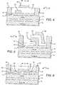
- FIGs. 3 and 4show another embodiment of a HEMT 40 according to the present invention that is similar to the HEMT 10 in FIGs. 1 and 2 .
- the HEMT 40comprises a substrate 12, nucleation layer 14, buffer layer 16, 2DEG 17, barrier layer 18, source contact 20, and drain contact 22.
- a gate 42is formed after formation of the barrier layer 18.
- a spacer/passivation layer 44is formed on the device and particularly over the gate 42 and the surface of the barrier layer 18 between the gate 42 and the source and drain contacts 20, 22.
- the spacer/passivation layercan be included only over the gate 42 and the surface of the barrier layer 18 between the gate 42 and the drain contact 22.
- a field plate 46is then formed on the spacer/passivation layer 44 overlapping the gate 42 and extending a distance L f in the gate-drain region.
- the spacer/passivation layer 44serves as a spacer layer for the field plate 46. The overlap of the field plate 46 over the gate 42 and the distance L f can be varied for optimum results.
- the field plate 46can be electrically connected to gate 42 and FIG. 3 shows two alternative gate connection structures that can be used, although it is understood that other connection structures can also be used.
- the field plate 46can be connected to the gate 42 through a first conductive path 48 running outside the active area of the HEMT 40 to a gate contact 50 that is used to make electrical contact to the gate 42.
- a second conductive path 52(shown in phantom) can also be used that runs outside of the active region of the HEMT 40 on the side opposite the gate contact 50.
- the conductive path 52is coupled between the gate .42 and the field plate 46.
- Conductive vias(not shown) can also be used to connect the field plate 46 to the gate 42, with each vias running between the two through the passivation layer 44. The vias can be arranged periodically down the field plate 46 to provide for effective current spreading from the gate 42 to the field plate 46.
- the field plate 46can extend different distances L f over the barrier layer from the edge of the gate 42, with a suitable range of distances being 0.1 to 1.5 ⁇ m, although other distances can also be used. In some embodiments, the field plate 46 can extend a distance L f of 0.2 to 1 ⁇ m. In other embodiments, the field plate 46 can extend a distance L f of 0.5 to 0.9 ⁇ m. In preferred embodiments, the field plate 46 can extend a distance L f of approximately 0.7 ⁇ m.
- FIG. 5shows another embodiment of a HEMT 60 according to the present invention that has many features similar to those in HEMTs 10 and 40, including a substrate 12, nucleation layer 14, buffer layer 16, 2DEG 17, barrier layer 18, source contact 20, and drain contact 22.
- HEMT 60has a gamma ( ⁇ ) shaped gate 62 that is particularly adapted to high frequency operation.
- the gate lengthis one of the important device dimensions in determining the speed of the device, and with higher frequency devices the gate length is shorter. Shorter gate contacts lead to high resistance that can negatively impact high frequency operation.
- T-gatesare commonly used in high frequency operation, but it can be difficult to achieve a well-coupled placement of a field plate with a T-gate.
- the gamma gate 62provides for low gate resistance and allows for controlled definition of the gate footprint.
- a spacer/passivation layer 64is included that covers the gamma gate 62 and the surface of barrier layer 18 between the gamma gate 62 and the source and drain contacts 20, 22. A space can remain between the horizontal portion of the gamma gate 62 and the top of the spacer layer.
- the HEMT 60also includes a field plate 66 on the spacer layer 64 that overlaps that gamma gate 62, with the field plate 66 preferably deposited on the side of the gamma gate not having a horizontal overhanging section. This arrangement allows for tight placement and effective coupling between the field plate and the active layers below it.
- the field plate 66can be electrically connected to the gate 62 in many different ways.
- a first conductive path(not shown) can be included between the field plate 66 and the gate contact or a second conductive path (not shown) can be included between field plate 66 and the gate 62, with both the conductive paths being outside the active area of the HEMT.
- Conductive viascan also be used between the field plate 66 and gate 62 that pass through the spacer layer 64.
- FIG. 6shows another embodiment of a HEMT 80 according to the present invention that is similar to HEMT 10 shown in FIG. 1 , and also comprises a substrate 12, nucleation layer 14, buffer layer 16, 2DEG 17, barrier layer 18, source contact 20, drain contact 22, spacer layer 24, and gate 26 with a field plate structure 28.
- the HEMT 80also includes a doped n + contact layer 82 formed on the spacer layer 24. Prior to formation of gate contact 26, contact layer 82 is etched to reveal a portion of the surface of spacer layer 24. A smaller portion of the spacer layer 24 can then be etched down to the barrier layer 18. The contact layer 82., spacer layer 24 and barrier layer can also be etched down to the buffer layer 16 so that source and drain contacts 20, 22 can be deposited. Contact layer 82 facilitates formation of ohmic source and drain contacts 20, 22 as well as providing low access region resistances.
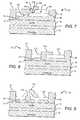
- FIG. 7shows another embodiment of a HEMT 90 according to the present invention having a substrate 12, nucleation layer 14, buffer layer 16, 2DEG 17, barrier layer 18, source contact 20 and drain contact 22 similar to those in the HEMTs described above.
- the HEMT 90also comprises a gate 92 and a field plate 94.
- the HEMT 90comprises multiple spacer layers 95, in this case two, although it is understood that more spacer layers can be used.
- a first spacer layer 96is formed on the barrier layer 18 at least between the gate 92 and the drain contact 22, with a preferred spacer layer also on the barrier layer 18 between the gate 92 and source contact 20.
- a second spacer layer 98is formed on the first spacer layer 96 and can be arranged in many different ways. It preferably covers less than all of the top surface of the first spacer layer 96 to form a step 100.
- the field plate 94is formed on the spacer layers, and because of the step 100, the field plate 94 essentially comprises first and second field plates portions 102, 104 each of which has a different spacing between it and the barrier layer 18.
- the first and second spacer layers 96, 98can comprise many different materials, with the layers typically comprising epitaxial materials or dielectric materials, such as SiN and SiO.
- the first spacer layer 96can be an epitaxial material and the second spacer layer 98 can be a dielectric material.
- the first spacer layer 96can again be an epitaxial material, and the second spacer layer 98 can also be an epitaxial material of the same or different material as the first spacer layer 96.
- first spacer layer 96comprise a dielectric material and the second spacer layer 98 comprise an epitaxial layer, although depending on the type of dielectric material used it can be difficult to form the second (epitaxial) layer 98 because of crystal structure loss.
- Better field plate couplingis typically provided using an epitaxial material, but the capacitance introduced by an epitaxial material can be higher than that of a dielectric material.
- the HEMT 90can exhibit its improved operating characteristics at two different voltages, with the first field plate 102 allowing improved operation of the HEMT 90 at one voltage and the second field plate 104 allowing improved operation at a higher second voltage.
- the physical dimensions and dielectric constant of the layer 102 under the first field plate 102is the same. The consistent dimensions and dielectric constant allow for the first field plate to provide improved HEMT 90 operating characteristics at a first voltage.
- the second layer 98is made of a dielectric material it generally has a lower dielectric constant than the epitaxial material in the first layer 96. As a result, the overall dielectric constant of the material under the second field plate 104 will be lower than the dielectric constant of the material under the first field plate 102. This results in lower capacitance and reduced coupling. The greater distance between the second field plate 104 and the barrier layer 18 along with the lowered dielectric constant results in the second field plate 104 providing improved operating characteristics at a higher voltage.
- the dielectric constant below the first and second field plates 102, 104remains the same, but the increased distance between the second field plate 104 and barrier layer 18 still provides improved operating characteristics at a higher voltage.
- the higher operating voltageis typically different than it would be if the second spacer layer were a dielectric material.
- the gate 92, field plate 102, 104, and spacer layers 94, 96can be formed in many different ways, with one formation method being depositing the first (epitaxial) spacer layer 94 on the barrier layer 18 and then etching the barrier layer to provide a space for the gate 92.
- the gate 92can then be deposited and the second spacer layer 96 can be deposited on the first 96.
- the second spacer layer 96can be etched before deposition of the gate 92.
- the first and second spacer layers 96, 98can be deposited on then etched in two etch steps; the first etch through both the layers 96, 98 and the second through the second layer 98 to form the step 100.
- the gate 92can then be deposited and the field plates 102, 104 can then be deposited over the first spacer and second spacer layers 96, 98.
- the first and second spacer layers 96, 98can be formed and then etched with the gate 92 and field plates formed in one or more formation steps.
- a single spacer layer of epitaxial or dielectric materialcan be etched to provide a step such that the resulting field plate has first and second portions.
- FIG. 8, 9 and 10show HEMTs 110, 130 and 140, respectively, with each HEMT having a substrate 12, nucleation layer 14, buffer layer 16, 2DEG 17, barrier layer 18, source contact 20 and drain contact 22 similar to those in the HEMTs described above.
- the HEMT 110( FIG. 8 ) is similar to the HEMT 10 in FIGs. 1 and 2 except that its gate 112 is recessed in the barrier layer 18.
- the HEMT's field plate 114is deposited on a spacer layer 116 and extend from the gate 112 toward the drain contact 22.
- the field plate 114provides the same operating improvements as the field plate 28 in HEMT 10.
- HEMT 130( FIG. 9 ) is similar to HEMT 40 in FIGs. 3 and 4 except that the gate 132 is recessed.
- the field plate 134is deposited on a spacer layer 136 and provides the same operating benefits.
- the HEMTs described hereincan also comprise gates that are only partially recessed.
- the HEMT 140is similar to the HEMT 130 except that its gate 142 is partially recessed. Its field plate 144 is deposited on a spacer layer 146 and provides the same operating benefits.
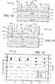
- FIG. 11shows still another embodiment of a HEMT 150 according to the present invention having a substrate 12, nucleation layer 14, buffer layer 16, 2DEG, 17, barrier layer 18, source contact 20 and drain contact 22.
- the HEMT 150also has a gate 152, spacer layer 154, and, integral field plate 156.
- the HEMT 150further comprises a second spacer layer 158 covering the field plate 156, spacer layer 154 and portion of the gate 152 above the spacer layer 154.
- a second field plate 159is on the second spacer layer 158 extending generally from the gate 152 toward the drain 22, with the second field plate electrically coupled to the gate either by one or more vias (not shown) through the second spacer layer 158, or by one or more conductive paths formed outside of the active region of the HEMT 150.
- Other HEMTs according to the present inventioncan comprise additional spacer layer and field plate pairs, with one additional pair shown in phantom.
- the structurecan also be covered by a dielectric passivation layer (not shown).
- a GaN-based HEMT structure in accordance with the embodiment of FIGs. 3 and 4was constructed and tested, with the results of the testing shown in the graph 160 of FIG. 12 .
- Initial testingshowed a power density of 20.4 W/mm with 51% Power Added Efficiency (PAE) operating in class B at 82V and 4GHz. More recent testing has achieved improved performance with a power density of 32W/mm with 55% PAE at 120V and 4Ghz.
- PAEPower Added Efficiency
- the effect of field plate distance (L f ) on device performancewas tested.
- the field plate length L fwas varied from a distance of 0 to 0.9 ⁇ m and the PAE of the resulting devices was then measured.
- the PAEshowed improvement once the field plate length was extended to 0.5 ⁇ m, with an optimum length of about 0.7 ⁇ m.
- the optimum lengthmay depend on the specific device design as well as operating voltage and frequency.
- FIG. 13shows one embodiment of a metal semiconductor field effect transistor (MESFET) 170 according to the present invention that is preferably silicon carbide (SiC) based, although MESFETs of other material systems can also be used.
- MESFET 170comprises a silicon carbide substrate 172 on which a silicon carbide buffer 174 and a silicon carbide channel layer 176 are formed with the buffer 174 sandwiched between the channel layer 176 and substrate 172.
- Source and drain contacts 178, 180are formed in contact with the channel layer 176.
- a non-conducting spacer layer 182is formed on the channel layer 176, between the source and drain contacts 178, 180. Similar to the spacer layer 24 described above and shown in FIGs. 1 and 2 , the spacer layer 182 can comprise a layer of non-conducting material such as a dielectric, or a number of different layers of non-conducting materials such as different dielectrics or epitaxial materials.
- the spacer layer 182can be etched to the channel layer 176 and a gate 184 can be deposited such that the bottom of the gate 184 is on the surface of channel layer 176.
- the metal forming the gate 184can be patterned to extend across spacer layer 182 so that the top of the gate 184 forms a field plate structure 186 extending a distance L f away from the edge of gate 184 towards drain contact 180.
- the structurecan be covered with a dielectric passivation layer 188, such as silicon nitride.
- FIG. 14shows another embodiment of a MESFET 190 according to the present invention that is similar to MESFET 170 in FIG. 12 , but has a gate and field plate structure similar to that in the HEMT 40 shown in FIGs. 3 and 4 .
- MESFET 190comprises a silicon carbide substrate 172, buffer 174, and channel 176. It also comprises a source contact 178, drain contact 180, and a gate 192 deposited on the channel 176.
- a spacer layer 194is deposited over the gate 192 and on the surface of the channel 176 between the gate 192 and the source and drain contacts 178, 180.
- a field plate 186is deposited on the spacer layer 194 and overlaps the gate 192.
- the field plate 196is coupled to the gate 192 by a conductive path as described above in HEMT 40 of FIGs. 3 and 4 .
- Many different conductive pathscan be used including a first conductive path to the gate contact (not shown) or a second conductive path (not shown) to the gate 192, both of which run outside of the MESFET active area.
- the field 196can also be coupled to the gate 192 by conductive vias (not shown) through the spacer layer 194.
- FIG. 15shows one embodiment of a MESFET 200 according to the present invention, with a recessed gate 202. Similar to the MESFETs 170 and 190 shown in FIGs. 12 and 13 , MESFET 200 also has a silicon carbide substrate 172, buffer 174, channel 176, a source contact 178 and a drain contact 180. The gate 202 deposited on the channel 176. A spacer layer 204 is deposited over the gate 202 on the surface of the channel 176 between the gate 202 and the source and drain contacts 178, 180. The spacer layer 204 is thinner than the spacer layer 194 in FIG.
- the gate 202is partially recessed in the channel 176 and a field plate 206 is deposited on the spacer layer 204, overlapping the gate 202.
- the field plate 206is coupled to the gate 202 by one or more conductive paths such as those described in HEMT 40 in FIGs. 3 and 4 .
- MESFETs according to the present inventioncan comprise multiple spacer layers as described HEMT 90 of FIG. 7 .
- the MESFETscan have two spacer layers in a stepped arrangement, although more than two spacer layers can be used.
- the layerscan comprise epitaxial or dielectric materials as also, described above, with the stepped arrangement effectively providing two field plates that provide improved operating characteristics at two voltages.
- MESFETs according to the present inventioncan also comprise multiple spacer layers and field plates similar to those on the HEMT 150 shown in FIG. 11 and described above.
Landscapes
- Junction Field-Effect Transistors (AREA)
Abstract
Description
- This application claims the benefit of provisional
application Serial Number 60/501,576 to Parikh et al. - The present invention relates to transistors and particularly to transistors utilizing field plates.
- High electron mobility transistors (HEMTs) are a common type of solid state transistor that are regularly fabricated from semiconductor materials such as Silicon (Si) or Gallium Arsenide (GaAs). One disadvantage of Si is that it has low electron mobility (600 - 1450 cm2/V-s), which produces a high source resistance. This resistance can degrade the Si based HEMT's high performance gain.
- GaAs based HEMTs have become the standard for signal amplification in civil and military radar, handset cellular, and satellite communications. GaAs has a higher electron mobility (approximately 6000 cm2/V-s) and a lower source resistance than Si, which allows GaAs based devices to function at higher frequencies. However, GaAs has a relatively small bandgap (1.42 eV at room temperature) and relatively small breakdown voltage, which prevents GaAs based HEMTs from providing high power at high frequencies.
- Improvements in the manufacturing of wide bandgap semiconductor materials such as AlGaN/GaN, has focused interest on the development of AlGaN/GaN HEMTs for high frequency, high temperature and high power applications. AlGaN/GaN has large bandgaps, as well as high peak and saturation electron velocity values [B. Belmont, K. Kim and M. Shur, J.Appl.Phys. 74, 1818 (1993)]. AlGaN/GaN HEMTs can also have two dimensional electron gas (2DEG) sheet densities in excess of 1013/cm2 and relatively high electron mobility (up to 2019 cm2/Vs) [R. Gaska, J.W. Yang, A. Osinsky, Q. Chen, M.A. Khan, A.O. Orlov, G.L. Snider and M.S. Shur, Appl.Phys.Lett., 72, 707 (1998)]. These characteristics allow AIGaN/GaN HEMTs to provide very high voltage and high power operation at RF, microwave and millimeter wave frequencies.
- AlGaN/GaN HEMTs have been grown on sapphire substrates and have shown a power density of 4.6 W/mm and a total power of 7.6 W [Y.F. Wu et al., IEICE Trans.Electron., E-82-C, 1895 (1999)]. More recently, AIGaN/GaN HEMTs grown on SiC have shown a power density of 9.8 W/mm at 8 GHz [Y.F. Wu, D. Kapolnek, J.P. Ibbetson, P. Parikh, B.P. Keller and U.K. Mishra, IEEE Trans.Electron.Dev., 48, 586 (2001)] and a total output power of 22.9 at 9 GHz [M. Micovic, A Kurdoghlian, P. Janke, P. Hashimoto, D.W.S. Wong, J.S. Moon, L. McCray and C. Nguyen, IEEE Trans.Electron.Dev., 48, 591 (2001)].
U.S. Patent number 5,192,987 to Khan et al. discloses GaN/AlGaN based HEMTs grown on a buffer and a substrate. Other AlGaN/GaN HEMTs and field effect transistors (FETs) have been described byGaska et al., "High-Temperature Performance of AlGaN/GaN HFET's on SiC substrates," IEEE Electron Device Letters, Vol. 18,; andPing et al., "DC and Microwave Performance of High Current AlGaN Heterostructure Field Effect Transistors Grown on P-type SiC Substrates," IEEE Electron Devices Letters, Vol. 19, No. 2, February 1998, Page 54. Some of these devices have shown a gain-bandwidth product (fT) as high as 67 gigahertz [K. Chu et al. WOCSEMMAD, Monterey, CA (February 1998)] and high power densities up to 2.84 W/mm at 10 GHz [G. Sullivan et al., "High Power 10-GHz Operation of AlGaN HFET's in Insulating SiC," IEEE Electron Device Letters, Vol. 19, No. 6, Page 198 (June 1998); andWu et al., IEEE Electron Device Letters, Volume 19, No. 2, Page 50 (February 1998)].- Electron trapping and the resulting difference between DC and RF characteristics have been a limiting factor in the performance of GaN based transistors, such as AlGaN/GaN HEMTs. Silicon Nitride (SiN) passivation has been successfully employed to alleviate this trapping problem, which has resulted in high performance devices with power densities over 10W/mm at 10 Ghz.
U.S. Patent No. 6,586,781 discloses methods and structures for reducing the trapping effect in GaN-based transistors. However, due to the high electric fields existing in these structures, charge trapping can still be an issue. - The present invention provides improved transistor structures utilizing gate connected field plates to improve operating characteristics. One transistor according to the present invention comprises a plurality of active semiconductor layers formed on a substrate. A source contact is formed in electrical contact with the plurality of active layers, and a drain contact is also formed in electrical contact with the plurality of active layers with space between the source and drain contacts on the topmost of the plurality of active layers. A gate is formed in electrical contact with the topmost of the plurality of active layers, between the source and drain contacts. A spacer layer of epitaxial material is formed on the surface of the topmost of the plurality of active layers, between the gate and the drain contact, wherein the gate is not covered by the spacer layer. A field plate is formed on the spacer layer integral to the gate.
- Another embodiment of a transistor according to the present invention comprises a plurality of active semiconductor layers formed on a substrate. A source contact is formed in electrical contact with the plurality of active layers. A drain contact is also formed in electrical contact with the plurality of active layers with space between the source and drain contacts on the topmost of the plurality of active layers. A gate is formed in electrical contact with the topmost of the plurality of active layers, between the source and drain contacts. A spacer layer is formed on the surface of the topmost of the plurality of active layers, between the gate and the drain contact, and covering the gate contact. A field plate is formed on the spacer layer and is electrically connected to the gate.
- Another embodiment of a transistor according to the present invention' comprises a plurality of active semiconductor layers formed on a substrate. Source and drain contacts are formed in electrical contact with the plurality of active layers. A gate is formed in electrical contact with the topmost of the plurality of active layers, between the source and drain contacts. A first spacer layer formed on the surface of the topmost of the plurality of active layers, between the gate and the drain contact, wherein the gate is not covered by the spacer layer. A first field plate formed on the spacer layer integral to the gate and extending toward the drain contact on the spacer layer. A second spacer layer covering the field plate and the surface of the spacer layer between the field plate and drain contact, and further comprising a second field plate on the second spacer layer and extending from the edge of the gate toward the drain contact.
- These and other further features and advantages of the invention would be apparent to those skilled in the art from the following detailed description, taking together with the accompanying drawings, in which:
FIG. 1 is a plan view of one embodiment of a HEMT according to the present invention;FIG. 2 is a sectional view of the HEMT inFIG. 1 ;FIG. 3 is a plan view of another embodiment of a HEMT according to the present invention;FIG. 4 is a sectional view of the HEMT inFIG. 3 ;FIG. 5 is a sectional view of another embodiment of a HEMT according to the present invention having a gamma shaped gate;FIG. 6 is a sectional view of another embodiment of a HEMT according to the present invention having an n+ doped contact layer;FIG. 7 is a sectional view of another embodiment of a HEMT according to the present invention having multiple spacer layers;FIG. 8 is a sectional view of another embodiment of a HEMT according to the present invention having a recessed gate;FIG. 9 is a sectional view of another embodiment of a HEMT according to the present invention having a recessed gate;FIG. 10 is a sectional view of another embodiment of a HEMT according to the present invention having a recessed gate;FIG. 11 is a sectional view of another embodiment of a HEMT according to the present invention having multiple field plates;FIG. 12 is a graph showing the performance of certain HEMTs arranged according to the present invention;FIG. 13 is a sectional view of one embodiment of a MESFET according to the present invention;FIG. 14 is a sectional view of another embodiment of a MESFET according to the present invention; andFIG. 15 is still another embodiment of a MESFET according to the present invention having a recessed gate.- The field plate arrangements according to the present invention can be used with many different transistor structures. Wide bandgap transistor structures generally include an active region, with metal source and drain contacts formed in electrical contact with the active region, and a gate contact formed between the source and drain contacts for modulating electric fields within the active region. A spacer layer is formed above the active region. The spacer layer can comprise a dielectric layer, a layer of epitaxial material such as an undoped or depleted wide bandgap epitaxial material, or a combination thereof. A conductive field plate is formed above the spacer layer and extends a distance Lf from, the edge of the gate contact toward the drain contact. The field plate can be electrically connected to the gate contact. This field plate arrangement can reduce the peak electric field in the device, resulting in increased breakdown voltage and reduced trapping. The reduction of the electric field can also yield other benefits such as reduced leakage currents and enhanced reliability.
- One type of transistor that can utilize the field plate arrangement according to the present invention is a high electron mobility transistor (HEMT), which typically includes a buffer layer and a barrier layer on the buffer layer. A two dimensional electron gas (2DEG) layer/channel is formed at the junction between the buffer layer and the barrier layer. A gate contact is formed on the barrier layer between the source and drain contacts and according to the present invention, a spacer layer is formed on the barrier layer at least between the gate and drain contact. It can also cover the barrier layer between the gate and source contact. The spacer layer can be formed before or after formation of the gate contact. The spacer layer can comprise a dielectric layer, a layer of undoped or depleted material Group III nitride material, or a combination thereof. Different Group III elements can be used in the spacer layer such as alloys of Al, Ga, or In, with a suitable spacer layer material being AlxGa1-xN (0 ≤ x ≤ 1). A conductive field plate is formed above the spacer layer and extends a distance Lf from the edge of the gate towards the drain contact. In some embodiments, the field plate is formed during the same deposition step as an extension of the gate contact. In other embodiments, the field plate and gate electrode are formed during separate deposition steps. The field plate can be electrically connected to the gate contact. In still other embodiments the field plate can be connected to the source contact.
- Another type of transistor that can utilize a field plate arrangement according to the present invention is a metal semiconductor field effect transistor (MESFET), which typically comprises a buffer layer on a substrate and a channel layer on the buffer layer with the buffer layer between the substrate and channel layer. A source contact is included in ohmic contact with the channel layer and a drain contact is also included in ohmic contact with the channel layer. A space on the channel layer remains between the source and drain contacts with a gate included on the channel layer between the source and drain contacts. A spacer layer is included on the channel layer at least between the gate and drain contact. The spacer layer can also cover the space between the gate and source contact. A field plate is included on the spacer layer and in electrical contact with the gate.
- This field plate arrangement for both the HEMT and MESFET can reduce the peak electric field in the device, compared to a device without a field plate, which can result in increased breakdown voltage and reduced trapping. The reduction of the electric field can also yield other benefits such as reduced leakage currents and enhanced reliability.
FIGs. 1 and 2 show one embodiment of a nitride basedHEMT 10 according to the present invention that comprises asubstrate 12 which can be made of silicon carbide, sapphire, spinet, ZnO, silicon, gallium nitride, aluminum nitride, or any other material capable of supporting growth of a Group-III nitride material. In some embodiments, thesubstrate 12 can comprise semiinsulating 4H-SiC commercially available from Cree, Inc. of Durham, NC.- A
nucleation layer 14 can be formed on thesubstrate 12 to reduce the lattice mismatch between thesubstrate 12 and the next layer in theHEMT 10. Thenucleation layer 14 should be approximately 1000 angstroms (Å) thick, although other thicknesses can be used. The nucleation layers 14 can comprise many different materials, with a suitable material being AlzGa1-zN (0<=z<=1). In one embodiment according to the present invention the nucleation layer comprises AlN (AlzGa1-zN, z=1).Nucleation layer 14 can be formed on thesubstrate 12 using known semiconductor growth techniques such as metal organic chemical vapor deposition (MOCVD), high vapor pressure epitaxy (HVPE) or molecular beam epitaxy (MBE). In still other embodiments, the nucleation layer can be formed as part of another layer in theHEMT 10, such as the buffer layer (described in detail below). - The formation of a
nucleation layer 14 can depend on the material used for thesubstrate 12. For example, methods of forming anucleation layer 14 on various substrates are taught inU.S. Patents 5,290,393 and5, 686, 738 , each of which are incorporated by reference as if fully set forth herein. Methods of forming nucleation layers on silicon carbide substrates are disclosed inU.S. Patents 5,393,993 ,5,523,589 , and5,739,554 each of which is incorporated herein by reference as if fully set forth herein. - The
HEMT 10 further comprises a highresistivity buffer layer 16 formed on thenucleation layer 14, with asuitable buffer layer 16 made of a Group III-nitride material such as AlxGayIn(1-x-y)N (0<=x<=1, 0<=y<=1, x+y<=1). In another embodiment according to the present invention thebuffer layer 16 comprises a GaN layer that is approximately 2µm thick, with part of the layer doped with Fe. - A
barrier layer 18 is formed on thebuffer layer 16 such that thebuffer layer 16 is sandwiched between thebarrier layer 18 and thenucleation layer 14. Each of thebuffer layer 16 andbarrier layer 18 can comprise doped or undoped layers of Group III-nitride materials. Thebarrier layer 18 can comprise one of more layers of different materials such as InGaN, AlGaN, AlN, or combinations thereof. In one embodiment thebarrier layer 18 comprises 0.8 nm of AlN and 22.5 nm of AlxGa1-xN (x≈0.195, as measured by photo luminescence). Exemplary structures are illustrated inU.S. Patent Nos. 6,316,793 ,6,586,781 ,6,548,333 andU.S. Published Patent Application Nos. 2002/0167023 and2003/00020092 U.S. Patents 5,192,987 and5,296,395 each of which is incorporated herein by reference as if fully set forth herein. The buffer and barrier layers 16, 18 can be made using the same methods used to grow thenucleation layer 14. A two dimensional electron gas (2DEG) layer/channel 17 is formed at the heterointerface between the buffer andbarrier layer - Metal source and
drain contacts barrier layer 18. Aspacer layer 24 can be formed on the surface of thebarrier layer 18 between the source anddrain contacts spacer layer 24 can comprise a layer of non-conducting material such as a dielectric (SiN or sio), or a number of different layers of non-conducting materials such as different dielectrics. In alternative embodiments the spacer layer can comprise one or more layers of epitaxial material alone or in combination with layers of dielectric material. The spacer layer can be many different thicknesses, with a suitable range of thicknesses being approximately 0.05 to 0.5 microns. Thespacer layer 24 is primarily arranged to allow a field plate to be deposited on it, with the field plate extending from thegate 26 toward thedrain contact 22. Accordingly, in some embodiments according to the present invention thespacer layer 24 can be included only on the surface of thebarrier layer 18 between thegate 26 anddrain contact 22. - In embodiments where the
spacer layer 24 covers thebarrier layer 18 between the source anddrain contacts spacer layer 24 can be etched to thebarrier layer 18 and agate electrode 26 deposited such that the bottom of thegate electrode 26 is on the surface ofbarrier layer 18. In embodiments where thespacer layer 24 only covers a portion of thebarrier layer 18, thegate 26 can be deposited on thebarrier layer 18 adjacent to thespacer layer 24. In still other embodiments, thegate 26 can be deposited before thespacer layer 24. - A
field plate 28 can be formed integral to the gate by the metal forming the gate electrode being patterned to extend acrossspacer layer 24 so that the top of thegate 26 forms afield plate structure 28 extending a distance Lf away from the edge ofgate 26 towardsdrain 22. Stated differently, the part of the gate metal resting on thespacer layer 24 forms afield plate 28. The structure can then be covered with adielectric passivation layer 30 such as silicon nitride. Methods of forming thedielectric passivation 30 are described in detail in the patents and publications referenced above. - Electric current can flow between the source and
drain contacts channel 17 when thegate 26 is biased at the appropriate level. The source anddrain contacts gate 26 can also be made of different materials including but not limited to gold, nickel, platinum, palladium, iridium, titanium, chromium, alloys of titanium and tungsten, or platinum silicide. Thegate 26 can have many different lengths, with a suitable range of gate lengths being 0.01 to 2 microns. In one embodiment according to the present invention a preferred gate length (Lg) is approximately 0.5 microns. In some embodiments, thefield plate 28 is formed during the same deposition step as an extension of thegate 26. In other embodiments, thefield plate 28 andgate 26 are formed during separate deposition steps. The formation of source anddrain contacts - The
field plate 28 can extend different distances Lf over the barrier layer from the edge of thegate 26 with a suitable range of distances being 0.1 to 1.5 µm, although other distances can also be used. Thefield plate 28 can comprise many different conductive materials with a suitable material being a metal, such as the same metal used for thegate 26. Thegate 26 andfield plate 28 can be deposited using standard metallization methods. FIGs. 3 and4 show another embodiment of aHEMT 40 according to the present invention that is similar to theHEMT 10 inFIGs. 1 and 2 . For the same or similar features for theHEMT 40 inFIG. 3 and4 , and the figures that follow, the same reference numerals fromFIGs. 1 and 2 will be used. TheHEMT 40 comprises asubstrate 12,nucleation layer 14,buffer layer 16,2DEG 17,barrier layer 18,source contact 20, and draincontact 22. Agate 42 is formed after formation of thebarrier layer 18. A spacer/passivation layer 44 is formed on the device and particularly over thegate 42 and the surface of thebarrier layer 18 between thegate 42 and the source anddrain contacts gate 42 and the surface of thebarrier layer 18 between thegate 42 and thedrain contact 22. Afield plate 46 is then formed on the spacer/passivation layer 44 overlapping thegate 42 and extending a distance Lf in the gate-drain region. In the embodiment shown inFIGs. 3 and4 , the spacer/passivation layer 44 serves as a spacer layer for thefield plate 46. The overlap of thefield plate 46 over thegate 42 and the distance Lf can be varied for optimum results.- The
field plate 46 can be electrically connected togate 42 andFIG. 3 shows two alternative gate connection structures that can be used, although it is understood that other connection structures can also be used. Thefield plate 46 can be connected to thegate 42 through a firstconductive path 48 running outside the active area of theHEMT 40 to agate contact 50 that is used to make electrical contact to thegate 42. A second conductive path 52 (shown in phantom) can also be used that runs outside of the active region of theHEMT 40 on the side opposite thegate contact 50. Theconductive path 52 is coupled between the gate .42 and thefield plate 46. Conductive vias (not shown) can also be used to connect thefield plate 46 to thegate 42, with each vias running between the two through thepassivation layer 44. The vias can be arranged periodically down thefield plate 46 to provide for effective current spreading from thegate 42 to thefield plate 46. - As in
HEMT 10 inFIGs. 1 and 2 , thefield plate 46 can extend different distances Lf over the barrier layer from the edge of thegate 42, with a suitable range of distances being 0.1 to 1.5 µm, although other distances can also be used. In some embodiments, thefield plate 46 can extend a distance Lf of 0.2 to 1 µm. In other embodiments, thefield plate 46 can extend a distance Lf of 0.5 to 0.9 µm. In preferred embodiments, thefield plate 46 can extend a distance Lf of approximately 0.7 µm. FIG. 5 shows another embodiment of aHEMT 60 according to the present invention that has many features similar to those inHEMTs substrate 12,nucleation layer 14,buffer layer 16,2DEG 17,barrier layer 18,source contact 20, and draincontact 22.HEMT 60, however, has a gamma (Γ) shapedgate 62 that is particularly adapted to high frequency operation. The gate length is one of the important device dimensions in determining the speed of the device, and with higher frequency devices the gate length is shorter. Shorter gate contacts lead to high resistance that can negatively impact high frequency operation. T-gates are commonly used in high frequency operation, but it can be difficult to achieve a well-coupled placement of a field plate with a T-gate.- The
gamma gate 62 provides for low gate resistance and allows for controlled definition of the gate footprint. A spacer/passivation layer 64 is included that covers thegamma gate 62 and the surface ofbarrier layer 18 between thegamma gate 62 and the source anddrain contacts gamma gate 62 and the top of the spacer layer. TheHEMT 60 also includes afield plate 66 on thespacer layer 64 that overlaps thatgamma gate 62, with thefield plate 66 preferably deposited on the side of the gamma gate not having a horizontal overhanging section. This arrangement allows for tight placement and effective coupling between the field plate and the active layers below it. - Like the
field plate 46 shown inFIGs . 3 and4 and described above, thefield plate 66 can be electrically connected to thegate 62 in many different ways. A first conductive path (not shown) can be included between thefield plate 66 and the gate contact or a second conductive path (not shown) can be included betweenfield plate 66 and thegate 62, with both the conductive paths being outside the active area of the HEMT. Conductive vias can also be used between thefield plate 66 andgate 62 that pass through thespacer layer 64. FIG. 6 shows another embodiment of a HEMT 80 according to the present invention that is similar toHEMT 10 shown inFIG. 1 , and also comprises asubstrate 12,nucleation layer 14,buffer layer 16,2DEG 17,barrier layer 18,source contact 20,drain contact 22,spacer layer 24, andgate 26 with afield plate structure 28. The HEMT 80 also includes a doped n+ contact layer 82 formed on thespacer layer 24. Prior to formation ofgate contact 26,contact layer 82 is etched to reveal a portion of the surface ofspacer layer 24. A smaller portion of thespacer layer 24 can then be etched down to thebarrier layer 18. The contact layer 82.,spacer layer 24 and barrier layer can also be etched down to thebuffer layer 16 so that source anddrain contacts Contact layer 82 facilitates formation of ohmic source anddrain contacts FIG. 7 shows another embodiment of aHEMT 90 according to the present invention having asubstrate 12,nucleation layer 14,buffer layer 16,2DEG 17,barrier layer 18,source contact 20 anddrain contact 22 similar to those in the HEMTs described above. TheHEMT 90 also comprises agate 92 and afield plate 94. Instead of having a spacer layer, however, theHEMT 90 comprises multiple spacer layers 95, in this case two, although it is understood that more spacer layers can be used. Afirst spacer layer 96 is formed on thebarrier layer 18 at least between thegate 92 and thedrain contact 22, with a preferred spacer layer also on thebarrier layer 18 between thegate 92 andsource contact 20. Asecond spacer layer 98 is formed on thefirst spacer layer 96 and can be arranged in many different ways. It preferably covers less than all of the top surface of thefirst spacer layer 96 to form astep 100. Thefield plate 94 is formed on the spacer layers, and because of thestep 100, thefield plate 94 essentially comprises first and secondfield plates portions barrier layer 18.- The first and second spacer layers 96, 98 can comprise many different materials, with the layers typically comprising epitaxial materials or dielectric materials, such as SiN and SiO. In one embodiment according to the present invention, the
first spacer layer 96 can be an epitaxial material and thesecond spacer layer 98 can be a dielectric material. In another embodiment thefirst spacer layer 96 can again be an epitaxial material, and thesecond spacer layer 98 can also be an epitaxial material of the same or different material as thefirst spacer layer 96. It may also be possible to have thefirst spacer layer 96 comprise a dielectric material and thesecond spacer layer 98 comprise an epitaxial layer, although depending on the type of dielectric material used it can be difficult to form the second (epitaxial)layer 98 because of crystal structure loss. Better field plate coupling is typically provided using an epitaxial material, but the capacitance introduced by an epitaxial material can be higher than that of a dielectric material. - By having first and
second field plates HEMT 90 can exhibit its improved operating characteristics at two different voltages, with thefirst field plate 102 allowing improved operation of theHEMT 90 at one voltage and thesecond field plate 104 allowing improved operation at a higher second voltage. For example, in embodiments of theHEMT 90 wherein thefirst spacer layer 102 is epitaxial (typically AlGaN or similar material), the physical dimensions and dielectric constant of thelayer 102 under thefirst field plate 102 is the same. The consistent dimensions and dielectric constant allow for the first field plate to provideimproved HEMT 90 operating characteristics at a first voltage. - If the
second layer 98 is made of a dielectric material it generally has a lower dielectric constant than the epitaxial material in thefirst layer 96. As a result, the overall dielectric constant of the material under thesecond field plate 104 will be lower than the dielectric constant of the material under thefirst field plate 102. This results in lower capacitance and reduced coupling. The greater distance between thesecond field plate 104 and thebarrier layer 18 along with the lowered dielectric constant results in thesecond field plate 104 providing improved operating characteristics at a higher voltage. - In those embodiments of the
HEMT 90 where the first andsecond layers second field plates second field plate 104 andbarrier layer 18 still provides improved operating characteristics at a higher voltage. The higher operating voltage, however, is typically different than it would be if the second spacer layer were a dielectric material. - The
gate 92,field plate spacer layer 94 on thebarrier layer 18 and then etching the barrier layer to provide a space for thegate 92. Thegate 92 can then be deposited and thesecond spacer layer 96 can be deposited on the first 96. In other embodiments thesecond spacer layer 96 can be etched before deposition of thegate 92. Alternatively, the first and second spacer layers 96, 98 can be deposited on then etched in two etch steps; the first etch through both thelayers second layer 98 to form thestep 100. Thegate 92 can then be deposited and thefield plates gate 92 and field plates formed in one or more formation steps. In still other embodiments a single spacer layer of epitaxial or dielectric material can be etched to provide a step such that the resulting field plate has first and second portions. - The gate and field plate structures according to the present invention can be used in many different ways beyond those shown in
FIGs. 1-7 above.FIG. 8, 9 and10 showHEMTs substrate 12,nucleation layer 14,buffer layer 16,2DEG 17,barrier layer 18,source contact 20 anddrain contact 22 similar to those in the HEMTs described above. The HEMT 110 (FIG. 8 ) is similar to theHEMT 10 inFIGs. 1 and 2 except that itsgate 112 is recessed in thebarrier layer 18. The HEMT'sfield plate 114 is deposited on aspacer layer 116 and extend from thegate 112 toward thedrain contact 22. Thefield plate 114 provides the same operating improvements as thefield plate 28 inHEMT 10. HEMT 130 (FIG. 9 ) is similar toHEMT 40 inFIGs. 3 and4 except that thegate 132 is recessed. Thefield plate 134 is deposited on aspacer layer 136 and provides the same operating benefits. The HEMTs described herein can also comprise gates that are only partially recessed. TheHEMT 140 is similar to theHEMT 130 except that itsgate 142 is partially recessed. Itsfield plate 144 is deposited on aspacer layer 146 and provides the same operating benefits. FIG. 11 shows still another embodiment of aHEMT 150 according to the present invention having asubstrate 12,nucleation layer 14,buffer layer 16, 2DEG, 17,barrier layer 18,source contact 20 anddrain contact 22. TheHEMT 150 also has agate 152,spacer layer 154, and,integral field plate 156. TheHEMT 150 further comprises asecond spacer layer 158 covering thefield plate 156,spacer layer 154 and portion of thegate 152 above thespacer layer 154. Asecond field plate 159 is on thesecond spacer layer 158 extending generally from thegate 152 toward thedrain 22, with the second field plate electrically coupled to the gate either by one or more vias (not shown) through thesecond spacer layer 158, or by one or more conductive paths formed outside of the active region of theHEMT 150. Other HEMTs according to the present invention can comprise additional spacer layer and field plate pairs, with one additional pair shown in phantom. The structure can also be covered by a dielectric passivation layer (not shown).- A GaN-based HEMT structure in accordance with the embodiment of
FIGs. 3 and4 was constructed and tested, with the results of the testing shown in thegraph 160 ofFIG. 12 . Initial testing showed a power density of 20.4 W/mm with 51% Power Added Efficiency (PAE) operating in class B at 82V and 4GHz. More recent testing has achieved improved performance with a power density of 32W/mm with 55% PAE at 120V and 4Ghz. - The effect of field plate distance (Lf) on device performance was tested. The field plate length Lf was varied from a distance of 0 to 0.9 µm and the PAE of the resulting devices was then measured. As illustrated in
FIG. 12 , the PAE showed improvement once the field plate length was extended to 0.5 µm, with an optimum length of about 0.7 µm. However, the optimum length may depend on the specific device design as well as operating voltage and frequency. - The field plate arrangements described above can be used in other types of transistors.
FIG. 13 shows one embodiment of a metal semiconductor field effect transistor (MESFET) 170 according to the present invention that is preferably silicon carbide (SiC) based, although MESFETs of other material systems can also be used.MESFET 170 comprises asilicon carbide substrate 172 on which asilicon carbide buffer 174 and a siliconcarbide channel layer 176 are formed with thebuffer 174 sandwiched between thechannel layer 176 andsubstrate 172. Source anddrain contacts channel layer 176. - A
non-conducting spacer layer 182 is formed on thechannel layer 176, between the source anddrain contacts spacer layer 24 described above and shown inFIGs. 1 and 2 , thespacer layer 182 can comprise a layer of non-conducting material such as a dielectric, or a number of different layers of non-conducting materials such as different dielectrics or epitaxial materials. - Also similar to the
spacer layer 24 inFIGs . 1 and 2 , thespacer layer 182 can be etched to thechannel layer 176 and agate 184 can be deposited such that the bottom of thegate 184 is on the surface ofchannel layer 176. The metal forming thegate 184 can be patterned to extend acrossspacer layer 182 so that the top of thegate 184 forms afield plate structure 186 extending a distance Lf away from the edge ofgate 184 towardsdrain contact 180. Finally, the structure can be covered with adielectric passivation layer 188, such as silicon nitride. - The fabrication of silicon carbide based MESFET devices is described in more detail in
U.S. Patent No. 5,686,737 andU.S Patent Application Ser. No. 09/567,717 filed May 10, 2000 FIG. 14 shows another embodiment of aMESFET 190 according to the present invention that is similar toMESFET 170 inFIG. 12 , but has a gate and field plate structure similar to that in theHEMT 40 shown inFIGs. 3 and4 .MESFET 190 comprises asilicon carbide substrate 172,buffer 174, andchannel 176. It also comprises asource contact 178,drain contact 180, and agate 192 deposited on thechannel 176. Aspacer layer 194 is deposited over thegate 192 and on the surface of thechannel 176 between thegate 192 and the source anddrain contacts field plate 186 is deposited on thespacer layer 194 and overlaps thegate 192. Thefield plate 196 is coupled to thegate 192 by a conductive path as described above inHEMT 40 ofFIGs. 3 and4 . Many different conductive paths can be used including a first conductive path to the gate contact (not shown) or a second conductive path (not shown) to thegate 192, both of which run outside of the MESFET active area. Thefield 196 can also be coupled to thegate 192 by conductive vias (not shown) through thespacer layer 194.- Just as with the HEMTs above, different embodiments of MESFETs according to the present invention can comprise recessed gates.
FIG. 15 shows one embodiment of aMESFET 200 according to the present invention, with a recessedgate 202. Similar to theMESFETs FIGs. 12 and13 ,MESFET 200 also has asilicon carbide substrate 172,buffer 174,channel 176, asource contact 178 and adrain contact 180. Thegate 202 deposited on thechannel 176. Aspacer layer 204 is deposited over thegate 202 on the surface of thechannel 176 between thegate 202 and the source anddrain contacts spacer layer 204 is thinner than thespacer layer 194 inFIG. 14 such that it conforms more closely to the shape of thegate 202. Thegate 202 is partially recessed in thechannel 176 and afield plate 206 is deposited on thespacer layer 204, overlapping thegate 202. Thefield plate 206 is coupled to thegate 202 by one or more conductive paths such as those described inHEMT 40 inFIGs. 3 and4 . - It is also understood that different embodiments of MESFETs according to the present invention can comprise multiple spacer layers as described
HEMT 90 ofFIG. 7 . In some embodiments according to the present invention, the MESFETs can have two spacer layers in a stepped arrangement, although more than two spacer layers can be used. The layers can comprise epitaxial or dielectric materials as also, described above, with the stepped arrangement effectively providing two field plates that provide improved operating characteristics at two voltages. It is also understood that MESFETs according to the present invention can also comprise multiple spacer layers and field plates similar to those on theHEMT 150 shown inFIG. 11 and described above. - Although the present invention has been described in considerable detail with reference to certain preferred configurations thereof, other versions are possible. The field plate arrangement can be used in many different devices. The field plates can also have many different shapes and can be connected to the source contact in many different ways. Accordingly, the spirit and scope of the invention should not be limited to the preferred versions of the invention described above.
Claims (30)
Applications Claiming Priority (4)
| Application Number | Priority Date | Filing Date | Title |
|---|---|---|---|
| US50157603P | 2003-09-09 | 2003-09-09 | |
| US10/930,160US7501669B2 (en) | 2003-09-09 | 2004-08-31 | Wide bandgap transistor devices with field plates |
| EP04788642.9AEP1665385B1 (en) | 2003-09-09 | 2004-09-08 | Wide bandgap transistor devices with field plates |
| PCT/US2004/029345WO2005029589A1 (en) | 2003-09-09 | 2004-09-08 | Wide bandgap transistor devices with field plates |
Related Parent Applications (3)
| Application Number | Title | Priority Date | Filing Date |
|---|---|---|---|
| EP04788642.9Division | 2004-09-08 | ||
| EP04788642.9ADivision-IntoEP1665385B1 (en) | 2003-09-09 | 2004-09-08 | Wide bandgap transistor devices with field plates |
| EP04788642.9ADivisionEP1665385B1 (en) | 2003-09-09 | 2004-09-08 | Wide bandgap transistor devices with field plates |
Publications (2)
| Publication Number | Publication Date |
|---|---|
| EP2432021A1true EP2432021A1 (en) | 2012-03-21 |
| EP2432021B1 EP2432021B1 (en) | 2021-06-09 |
Family
ID=34228870
Family Applications (4)
| Application Number | Title | Priority Date | Filing Date |
|---|---|---|---|
| EP11183396.8AExpired - LifetimeEP2432021B1 (en) | 2003-09-09 | 2004-09-08 | A transistor with a field plate |
| EP11183404ACeasedEP2434546A1 (en) | 2003-09-09 | 2004-09-08 | A transistor with a field plate |
| EP11183655ACeasedEP2437303A1 (en) | 2003-09-09 | 2004-09-08 | A transistor with a field plate. |
| EP04788642.9AExpired - LifetimeEP1665385B1 (en) | 2003-09-09 | 2004-09-08 | Wide bandgap transistor devices with field plates |
Family Applications After (3)
| Application Number | Title | Priority Date | Filing Date |
|---|---|---|---|
| EP11183404ACeasedEP2434546A1 (en) | 2003-09-09 | 2004-09-08 | A transistor with a field plate |
| EP11183655ACeasedEP2437303A1 (en) | 2003-09-09 | 2004-09-08 | A transistor with a field plate. |
| EP04788642.9AExpired - LifetimeEP1665385B1 (en) | 2003-09-09 | 2004-09-08 | Wide bandgap transistor devices with field plates |
Country Status (7)
| Country | Link |
|---|---|
| US (4) | US7501669B2 (en) |
| EP (4) | EP2432021B1 (en) |
| JP (1) | JP2007505501A (en) |
| KR (1) | KR101108300B1 (en) |
| CN (2) | CN102306658A (en) |
| CA (1) | CA2536030A1 (en) |
| WO (1) | WO2005029589A1 (en) |
Families Citing this family (212)
| Publication number | Priority date | Publication date | Assignee | Title |
|---|---|---|---|---|
| US7230284B2 (en)* | 2001-07-24 | 2007-06-12 | Cree, Inc. | Insulating gate AlGaN/GaN HEMT |
| US7812369B2 (en)* | 2003-09-09 | 2010-10-12 | The Regents Of The University Of California | Fabrication of single or multiple gate field plates |
| US7501669B2 (en) | 2003-09-09 | 2009-03-10 | Cree, Inc. | Wide bandgap transistor devices with field plates |
| TWI295085B (en)* | 2003-12-05 | 2008-03-21 | Int Rectifier Corp | Field effect transistor with enhanced insulator structure |
| US7045404B2 (en)* | 2004-01-16 | 2006-05-16 | Cree, Inc. | Nitride-based transistors with a protective layer and a low-damage recess and methods of fabrication thereof |
| US8174048B2 (en)* | 2004-01-23 | 2012-05-08 | International Rectifier Corporation | III-nitride current control device and method of manufacture |
| US7550783B2 (en) | 2004-05-11 | 2009-06-23 | Cree, Inc. | Wide bandgap HEMTs with source connected field plates |
| US7573078B2 (en) | 2004-05-11 | 2009-08-11 | Cree, Inc. | Wide bandgap transistors with multiple field plates |
| US9773877B2 (en)* | 2004-05-13 | 2017-09-26 | Cree, Inc. | Wide bandgap field effect transistors with source connected field plates |
| US20060073621A1 (en)* | 2004-10-01 | 2006-04-06 | Palo Alto Research Center Incorporated | Group III-nitride based HEMT device with insulating GaN/AlGaN buffer layer |
| US9640649B2 (en)* | 2004-12-30 | 2017-05-02 | Infineon Technologies Americas Corp. | III-nitride power semiconductor with a field relaxation feature |
| WO2006080109A1 (en)* | 2005-01-25 | 2006-08-03 | Fujitsu Limited | Semiconductor device provided with mis structure and method for manufacturing the same |
| US11791385B2 (en)* | 2005-03-11 | 2023-10-17 | Wolfspeed, Inc. | Wide bandgap transistors with gate-source field plates |
| US20060223293A1 (en)* | 2005-04-01 | 2006-10-05 | Raytheon Company | Semiconductor devices having improved field plates |
| US7615774B2 (en)* | 2005-04-29 | 2009-11-10 | Cree.Inc. | Aluminum free group III-nitride based high electron mobility transistors |
| US20060255377A1 (en)* | 2005-05-12 | 2006-11-16 | Der-Wei Tu | Field effect transistor with novel field-plate structure |
| EP1901341A4 (en)* | 2005-06-10 | 2009-07-15 | Nec Corp | FIELD EFFECT TRANSISTOR |
| JP4968068B2 (en)* | 2005-06-10 | 2012-07-04 | 日本電気株式会社 | Field effect transistor |
| US20070018199A1 (en)* | 2005-07-20 | 2007-01-25 | Cree, Inc. | Nitride-based transistors and fabrication methods with an etch stop layer |
| US7548112B2 (en)* | 2005-07-21 | 2009-06-16 | Cree, Inc. | Switch mode power amplifier using MIS-HEMT with field plate extension |
| US8183595B2 (en)* | 2005-07-29 | 2012-05-22 | International Rectifier Corporation | Normally off III-nitride semiconductor device having a programmable gate |
| JP4751150B2 (en) | 2005-08-31 | 2011-08-17 | 株式会社東芝 | Nitride semiconductor devices |
| EP1938385B1 (en) | 2005-09-07 | 2014-12-03 | Cree, Inc. | Transistors with fluorine treatment |
| EP1932181A4 (en)* | 2005-09-16 | 2009-06-17 | Univ California | ENRICHMENT FIELD EFFECT TRANSISTOR, GALLIUM NITRIDE / ALUMINUM NITRIDE AND N-POLARITY GALLIUM |
| US20070138515A1 (en)* | 2005-12-19 | 2007-06-21 | M/A-Com, Inc. | Dual field plate MESFET |
| DE112007000092B4 (en)* | 2006-01-09 | 2014-07-24 | International Rectifier Corp. | Group III nitride power semiconductors with a field relaxation feature |
| US7709269B2 (en) | 2006-01-17 | 2010-05-04 | Cree, Inc. | Methods of fabricating transistors including dielectrically-supported gate electrodes |
| US7592211B2 (en) | 2006-01-17 | 2009-09-22 | Cree, Inc. | Methods of fabricating transistors including supported gate electrodes |
| US7408208B2 (en) | 2006-03-20 | 2008-08-05 | International Rectifier Corporation | III-nitride power semiconductor device |
| JP2009530862A (en)* | 2006-03-20 | 2009-08-27 | インターナショナル レクティファイアー コーポレイション | Merged gate cascode transistor |
| US7388236B2 (en) | 2006-03-29 | 2008-06-17 | Cree, Inc. | High efficiency and/or high power density wide bandgap transistors |
| KR100770132B1 (en)* | 2006-10-30 | 2007-10-24 | 페어차일드코리아반도체 주식회사 | Nitride-based semiconductor device |
| EP1921669B1 (en)* | 2006-11-13 | 2015-09-02 | Cree, Inc. | GaN based HEMTs with buried field plates |
| US7692263B2 (en) | 2006-11-21 | 2010-04-06 | Cree, Inc. | High voltage GaN transistors |
| JP4712683B2 (en)* | 2006-12-21 | 2011-06-29 | パナソニック株式会社 | Transistor and manufacturing method thereof |
| US7838904B2 (en)* | 2007-01-31 | 2010-11-23 | Panasonic Corporation | Nitride based semiconductor device with concave gate region |
| US8212290B2 (en) | 2007-03-23 | 2012-07-03 | Cree, Inc. | High temperature performance capable gallium nitride transistor |
| JP4691060B2 (en)* | 2007-03-23 | 2011-06-01 | 古河電気工業株式会社 | GaN-based semiconductor devices |
| JP5266679B2 (en)* | 2007-07-11 | 2013-08-21 | 住友電気工業株式会社 | Group III nitride electronic devices |
| US7609115B2 (en)* | 2007-09-07 | 2009-10-27 | Raytheon Company | Input circuitry for transistor power amplifier and method for designing such circuitry |
| US7915643B2 (en) | 2007-09-17 | 2011-03-29 | Transphorm Inc. | Enhancement mode gallium nitride power devices |
| US20090072269A1 (en)* | 2007-09-17 | 2009-03-19 | Chang Soo Suh | Gallium nitride diodes and integrated components |
| US7800132B2 (en)* | 2007-10-25 | 2010-09-21 | Northrop Grumman Systems Corporation | High electron mobility transistor semiconductor device having field mitigating plate and fabrication method thereof |
| WO2009073866A1 (en)* | 2007-12-07 | 2009-06-11 | The Government Of The United States Of America, As Represented By The Secretary Of The Navy | Gate after diamond transistor |
| US7750370B2 (en) | 2007-12-20 | 2010-07-06 | Northrop Grumman Space & Mission Systems Corp. | High electron mobility transistor having self-aligned miniature field mitigating plate on a protective dielectric layer |
| JP5134378B2 (en)* | 2008-01-07 | 2013-01-30 | シャープ株式会社 | Field effect transistor |
| US7965126B2 (en) | 2008-02-12 | 2011-06-21 | Transphorm Inc. | Bridge circuits and their components |
| US8519438B2 (en) | 2008-04-23 | 2013-08-27 | Transphorm Inc. | Enhancement mode III-N HEMTs |
| CN101604704B (en)* | 2008-06-13 | 2012-09-05 | 西安能讯微电子有限公司 | HEMT device and manufacturing method thereof |
| US7985986B2 (en)* | 2008-07-31 | 2011-07-26 | Cree, Inc. | Normally-off semiconductor devices |
| JP5408929B2 (en) | 2008-08-21 | 2014-02-05 | 昭和電工株式会社 | Semiconductor device and manufacturing method of semiconductor device |
| US8289065B2 (en) | 2008-09-23 | 2012-10-16 | Transphorm Inc. | Inductive load power switching circuits |
| US7898004B2 (en) | 2008-12-10 | 2011-03-01 | Transphorm Inc. | Semiconductor heterostructure diodes |
| US7884394B2 (en)* | 2009-02-09 | 2011-02-08 | Transphorm Inc. | III-nitride devices and circuits |
| US8823012B2 (en)* | 2009-04-08 | 2014-09-02 | Efficient Power Conversion Corporation | Enhancement mode GaN HEMT device with gate spacer and method for fabricating the same |
| US8742459B2 (en) | 2009-05-14 | 2014-06-03 | Transphorm Inc. | High voltage III-nitride semiconductor devices |
| JP5595685B2 (en)* | 2009-07-28 | 2014-09-24 | パナソニック株式会社 | Semiconductor device |
| US8390000B2 (en) | 2009-08-28 | 2013-03-05 | Transphorm Inc. | Semiconductor devices with field plates |
| US8138529B2 (en) | 2009-11-02 | 2012-03-20 | Transphorm Inc. | Package configurations for low EMI circuits |
| JP5625336B2 (en)* | 2009-11-30 | 2014-11-19 | サンケン電気株式会社 | Semiconductor device |
| JP5037594B2 (en)* | 2009-12-08 | 2012-09-26 | シャープ株式会社 | Field effect transistor |
| US8389977B2 (en) | 2009-12-10 | 2013-03-05 | Transphorm Inc. | Reverse side engineered III-nitride devices |
| US8816497B2 (en)* | 2010-01-08 | 2014-08-26 | Transphorm Inc. | Electronic devices and components for high efficiency power circuits |
| US8624662B2 (en) | 2010-02-05 | 2014-01-07 | Transphorm Inc. | Semiconductor electronic components and circuits |
| US20110241020A1 (en)* | 2010-03-31 | 2011-10-06 | Triquint Semiconductor, Inc. | High electron mobility transistor with recessed barrier layer |
| US8907350B2 (en)* | 2010-04-28 | 2014-12-09 | Cree, Inc. | Semiconductor devices having improved adhesion and methods of fabricating the same |
| EP2383786B1 (en) | 2010-04-29 | 2018-08-15 | Ampleon Netherlands B.V. | Semiconductor transistor comprising two electrically conductive shield elements |
| US8829999B2 (en) | 2010-05-20 | 2014-09-09 | Cree, Inc. | Low noise amplifiers including group III nitride based high electron mobility transistors |
| JP2011249728A (en)* | 2010-05-31 | 2011-12-08 | Toshiba Corp | Semiconductor device and method for manufacturing the same |
| US8809987B2 (en)* | 2010-07-06 | 2014-08-19 | The Hong Kong University Of Science And Technology | Normally-off III-nitride metal-2DEG tunnel junction field-effect transistors |
| JP5655424B2 (en)* | 2010-08-09 | 2015-01-21 | サンケン電気株式会社 | Compound semiconductor device |
| JP2012109492A (en)* | 2010-11-19 | 2012-06-07 | Sanken Electric Co Ltd | Compound semiconductor device |
| JP5707903B2 (en)* | 2010-12-02 | 2015-04-30 | 富士通株式会社 | Compound semiconductor device and manufacturing method thereof |
| US8742460B2 (en) | 2010-12-15 | 2014-06-03 | Transphorm Inc. | Transistors with isolation regions |
| US8643062B2 (en) | 2011-02-02 | 2014-02-04 | Transphorm Inc. | III-N device structures and methods |
| US8786327B2 (en) | 2011-02-28 | 2014-07-22 | Transphorm Inc. | Electronic components with reactive filters |
| US8716141B2 (en) | 2011-03-04 | 2014-05-06 | Transphorm Inc. | Electrode configurations for semiconductor devices |
| US8772842B2 (en) | 2011-03-04 | 2014-07-08 | Transphorm, Inc. | Semiconductor diodes with low reverse bias currents |
| US8803232B2 (en) | 2011-05-29 | 2014-08-12 | Taiwan Semiconductor Manufacturing Co., Ltd. | High voltage and ultra-high voltage semiconductor devices with increased breakdown voltages |
| US8901604B2 (en) | 2011-09-06 | 2014-12-02 | Transphorm Inc. | Semiconductor devices with guard rings |
| US9257547B2 (en) | 2011-09-13 | 2016-02-09 | Transphorm Inc. | III-N device structures having a non-insulating substrate |
| US8772833B2 (en)* | 2011-09-21 | 2014-07-08 | Electronics And Telecommunications Research Institute | Power semiconductor device and fabrication method thereof |
| US8598937B2 (en) | 2011-10-07 | 2013-12-03 | Transphorm Inc. | High power semiconductor electronic components with increased reliability |
| US20130105817A1 (en) | 2011-10-26 | 2013-05-02 | Triquint Semiconductor, Inc. | High electron mobility transistor structure and method |
| US8884308B2 (en) | 2011-11-29 | 2014-11-11 | Taiwan Semiconductor Manufacturing Company, Ltd. | High electron mobility transistor structure with improved breakdown voltage performance |
| US9209176B2 (en) | 2011-12-07 | 2015-12-08 | Transphorm Inc. | Semiconductor modules and methods of forming the same |
| US10002957B2 (en) | 2011-12-21 | 2018-06-19 | Power Integrations, Inc. | Shield wrap for a heterostructure field effect transistor |
| JP2013131650A (en)* | 2011-12-21 | 2013-07-04 | Fujitsu Ltd | Semiconductor device and method of manufacturing the same |
| US9165766B2 (en) | 2012-02-03 | 2015-10-20 | Transphorm Inc. | Buffer layer structures suited for III-nitride devices with foreign substrates |
| JP6147018B2 (en)* | 2012-02-23 | 2017-06-14 | エフィシエント パワー コンヴァーション コーポレーション | Enhancement mode GaN HEMT device with gate spacer and method of manufacturing the same |
| US8648643B2 (en) | 2012-02-24 | 2014-02-11 | Transphorm Inc. | Semiconductor power modules and devices |
| WO2013155108A1 (en) | 2012-04-09 | 2013-10-17 | Transphorm Inc. | N-polar iii-nitride transistors |
| US9443941B2 (en)* | 2012-06-04 | 2016-09-13 | Infineon Technologies Austria Ag | Compound semiconductor transistor with self aligned gate |
| US9184275B2 (en) | 2012-06-27 | 2015-11-10 | Transphorm Inc. | Semiconductor devices with integrated hole collectors |
| US8803246B2 (en) | 2012-07-16 | 2014-08-12 | Transphorm Inc. | Semiconductor electronic components with integrated current limiters |
| WO2014050054A1 (en)* | 2012-09-28 | 2014-04-03 | パナソニック株式会社 | Semiconductor device |
| JP6085442B2 (en) | 2012-09-28 | 2017-02-22 | トランスフォーム・ジャパン株式会社 | Compound semiconductor device and manufacturing method thereof |
| JP2014090037A (en)* | 2012-10-29 | 2014-05-15 | Advanced Power Device Research Association | Semiconductor device |
| CN105164811B (en) | 2013-02-15 | 2018-08-31 | 创世舫电子有限公司 | Electrode of semiconductor devices and forming method thereof |
| US9087718B2 (en) | 2013-03-13 | 2015-07-21 | Transphorm Inc. | Enhancement-mode III-nitride devices |
| US9245992B2 (en) | 2013-03-15 | 2016-01-26 | Transphorm Inc. | Carbon doping semiconductor devices |
| US9048184B2 (en)* | 2013-03-15 | 2015-06-02 | Northrop Grumman Systems Corporation | Method of forming a gate contact |
| US9059076B2 (en) | 2013-04-01 | 2015-06-16 | Transphorm Inc. | Gate drivers for circuits based on semiconductor devices |
| US9142626B1 (en) | 2013-04-23 | 2015-09-22 | Hrl Laboratories, Llc | Stepped field plate wide bandgap field-effect transistor and method |
| US9755059B2 (en) | 2013-06-09 | 2017-09-05 | Cree, Inc. | Cascode structures with GaN cap layers |
| US9847411B2 (en) | 2013-06-09 | 2017-12-19 | Cree, Inc. | Recessed field plate transistor structures |
| US9679981B2 (en) | 2013-06-09 | 2017-06-13 | Cree, Inc. | Cascode structures for GaN HEMTs |
| US9407214B2 (en) | 2013-06-28 | 2016-08-02 | Cree, Inc. | MMIC power amplifier |
| US9537425B2 (en) | 2013-07-09 | 2017-01-03 | Transphorm Inc. | Multilevel inverters and their components |
| US9455341B2 (en)* | 2013-07-17 | 2016-09-27 | Taiwan Semiconductor Manufacturing Company, Ltd. | Transistor having a back-barrier layer and method of making the same |
| US9443938B2 (en) | 2013-07-19 | 2016-09-13 | Transphorm Inc. | III-nitride transistor including a p-type depleting layer |
| TWI555209B (en) | 2013-07-29 | 2016-10-21 | 高效電源轉換公司 | Gallium nitride device with reduced output capacitance and method of manufacturing same |
| US10566429B2 (en)* | 2013-08-01 | 2020-02-18 | Dynax Semiconductor, Inc. | Semiconductor device and method of manufacturing the same |
| US10910491B2 (en) | 2013-09-10 | 2021-02-02 | Delta Electronics, Inc. | Semiconductor device having reduced capacitance between source and drain pads |
| US10236236B2 (en) | 2013-09-10 | 2019-03-19 | Delta Electronics, Inc. | Heterojunction semiconductor device for reducing parasitic capacitance |
| US10833185B2 (en) | 2013-09-10 | 2020-11-10 | Delta Electronics, Inc. | Heterojunction semiconductor device having source and drain pads with improved current crowding |
| TWI577022B (en) | 2014-02-27 | 2017-04-01 | 台達電子工業股份有限公司 | Semiconductor device and semiconductor device package using the same |
| US10665709B2 (en) | 2013-09-10 | 2020-05-26 | Delta Electronics, Inc. | Power semiconductor device integrated with ESD protection circuit under source pad, drain pad, and/or gate pad |
| KR102100928B1 (en)* | 2013-10-17 | 2020-05-15 | 삼성전자주식회사 | High electron mobility transistor |
| JP2015177016A (en)* | 2014-03-14 | 2015-10-05 | 株式会社東芝 | Semiconductor device |
| US8980759B1 (en) | 2014-05-22 | 2015-03-17 | Hrl Laboratories, Llc | Method of fabricating slanted field-plate GaN heterojunction field-effect transistor |
| US9543940B2 (en) | 2014-07-03 | 2017-01-10 | Transphorm Inc. | Switching circuits having ferrite beads |
| US9590494B1 (en) | 2014-07-17 | 2017-03-07 | Transphorm Inc. | Bridgeless power factor correction circuits |
| US9318593B2 (en) | 2014-07-21 | 2016-04-19 | Transphorm Inc. | Forming enhancement mode III-nitride devices |
| WO2016043748A1 (en) | 2014-09-18 | 2016-03-24 | Intel Corporation | Wurtzite heteroepitaxial structures with inclined sidewall facets for defect propagation control in silicon cmos-compatible semiconductor devices |
| US10229991B2 (en) | 2014-09-25 | 2019-03-12 | Intel Corporation | III-N epitaxial device structures on free standing silicon mesas |
| US9640623B2 (en) | 2014-10-17 | 2017-05-02 | Cree, Inc. | Semiconductor device with improved field plate |
| US9608078B2 (en) | 2014-10-17 | 2017-03-28 | Cree, Inc. | Semiconductor device with improved field plate |
| WO2016068935A1 (en)* | 2014-10-30 | 2016-05-06 | Intel Corporation | Source/drain regrowth for low contact resistance to 2d electron gas in gallium nitride transistors |
| US9559161B2 (en)* | 2014-11-13 | 2017-01-31 | Infineon Technologies Austria Ag | Patterned back-barrier for III-nitride semiconductor devices |
| US9590087B2 (en) | 2014-11-13 | 2017-03-07 | Infineon Technologies Austria Ag | Compound gated semiconductor device having semiconductor field plate |
| US9536967B2 (en) | 2014-12-16 | 2017-01-03 | Transphorm Inc. | Recessed ohmic contacts in a III-N device |
| US9536966B2 (en) | 2014-12-16 | 2017-01-03 | Transphorm Inc. | Gate structures for III-N devices |
| US10056456B2 (en) | 2014-12-18 | 2018-08-21 | Intel Corporation | N-channel gallium nitride transistors |
| JP2016171162A (en)* | 2015-03-12 | 2016-09-23 | 株式会社東芝 | Semiconductor device |
| WO2016149146A1 (en) | 2015-03-13 | 2016-09-22 | Transphorm, Inc. | Paralleling of switching devices for high power circuits |
| CN104882483B (en)* | 2015-05-05 | 2018-06-26 | 西安电子科技大学 | Field-effect transistor with Γ grid and recess buffer layer and preparation method thereof |
| CN104916684B (en)* | 2015-06-11 | 2018-04-27 | 大连理工大学 | A kind of longitudinal direction is short to open grid groove type HEMT device and preparation method thereof |
| CN108604596A (en) | 2015-07-17 | 2018-09-28 | 剑桥电子有限公司 | Field plate structure for semiconductor device |
| US10553689B2 (en) | 2015-12-23 | 2020-02-04 | Intel Corporation | Multiple stacked field-plated GaN transistor and interlayer dielectrics to improve breakdown voltage and reduce parasitic capacitances |
| US11322599B2 (en) | 2016-01-15 | 2022-05-03 | Transphorm Technology, Inc. | Enhancement mode III-nitride devices having an Al1-xSixO gate insulator |
| TWI762486B (en) | 2016-05-31 | 2022-05-01 | 美商創世舫科技有限公司 | Iii-nitride devices including a graded depleting layer |
| US10096702B2 (en) | 2016-06-01 | 2018-10-09 | Efficient Power Conversion Corporation | Multi-step surface passivation structures and methods for fabricating same |
| DE102016122399A1 (en)* | 2016-11-21 | 2018-05-24 | Forschungsverbund Berlin E.V. | Gate structure and method for its production |
| DE102016123934A1 (en) | 2016-12-09 | 2018-06-14 | United Monolithic Semiconductors Gmbh | Method for producing a transistor |
| DE102016123931A1 (en) | 2016-12-09 | 2018-06-14 | United Monolithic Semiconductors Gmbh | transistor |
| CN107134491B (en)* | 2017-03-29 | 2019-11-29 | 西安电子科技大学 | Vertical structure power electronic devices based on arcuate source field plate |
| CN107068740B (en)* | 2017-03-29 | 2019-12-03 | 西安电子科技大学 | Source echelon field plate vertical power transistor |
| CN107170820B (en)* | 2017-03-29 | 2020-04-14 | 西安电子科技大学 | Arc Gate-Drain Compound Field Plate Current Aperture Heterojunction Devices |
| CN107134490B (en)* | 2017-03-29 | 2020-04-14 | 西安电子科技大学 | Vertical power device based on arc-shaped source field plate and arc-shaped drain field plate and its fabrication method |
| US10319648B2 (en) | 2017-04-17 | 2019-06-11 | Transphorm Inc. | Conditions for burn-in of high power semiconductors |
| WO2019066953A1 (en) | 2017-09-29 | 2019-04-04 | Intel Corporation | Group iii-nitride (iii-n) devices with reduced contact resistance and their methods of fabrication |
| US12125888B2 (en) | 2017-09-29 | 2024-10-22 | Intel Corporation | Group III-nitride (III-N) devices with reduced contact resistance and their methods of fabrication |
| US10326002B1 (en)* | 2018-06-11 | 2019-06-18 | Globalfoundries Inc. | Self-aligned gate contact and cross-coupling contact formation |
| FR3088485B1 (en)* | 2018-11-13 | 2021-04-30 | Commissariat Energie Atomique | FIELD PLATE SEMICONDUCTOR DEVICE |
| CN109887836B (en)* | 2019-01-25 | 2021-03-02 | 西安交通大学 | Preparation method of field effect transistor with n-type doped single crystal diamond field plate structure |
| US11121245B2 (en) | 2019-02-22 | 2021-09-14 | Efficient Power Conversion Corporation | Field plate structures with patterned surface passivation layers and methods for manufacturing thereof |
| CN110010682B (en)* | 2019-03-22 | 2024-08-02 | 华南理工大学 | GaN-HEMT device with sandwich structure and preparation method thereof |
| US10971612B2 (en) | 2019-06-13 | 2021-04-06 | Cree, Inc. | High electron mobility transistors and power amplifiers including said transistors having improved performance and reliability |
| CN110581170A (en)* | 2019-08-13 | 2019-12-17 | 中山市华南理工大学现代产业技术研究院 | GaN-based MIS-HEMT device with Γ-type gate and its preparation method |
| US12032014B2 (en) | 2019-09-09 | 2024-07-09 | Analog Devices International Unlimited Company | Semiconductor device configured for gate dielectric monitoring |
| US11862691B2 (en) | 2019-11-01 | 2024-01-02 | Raytheon Company | Field effect transistor having field plate |
| US11552190B2 (en)* | 2019-12-12 | 2023-01-10 | Analog Devices International Unlimited Company | High voltage double-diffused metal oxide semiconductor transistor with isolated parasitic bipolar junction transistor region |
| CN113875019B (en) | 2020-04-30 | 2024-07-02 | 英诺赛科(苏州)半导体有限公司 | Semiconductor device and method of manufacturing the same |
| US11769768B2 (en) | 2020-06-01 | 2023-09-26 | Wolfspeed, Inc. | Methods for pillar connection on frontside and passive device integration on backside of die |
| US11228287B2 (en) | 2020-06-17 | 2022-01-18 | Cree, Inc. | Multi-stage decoupling networks integrated with on-package impedance matching networks for RF power amplifiers |
| US11533025B2 (en) | 2020-06-18 | 2022-12-20 | Wolfspeed, Inc. | Integrated doherty amplifier with added isolation between the carrier and the peaking transistors |
| US11581859B2 (en) | 2020-06-26 | 2023-02-14 | Wolfspeed, Inc. | Radio frequency (RF) transistor amplifier packages with improved isolation and lead configurations |
| US11887945B2 (en) | 2020-09-30 | 2024-01-30 | Wolfspeed, Inc. | Semiconductor device with isolation and/or protection structures |
| US11749726B2 (en) | 2020-10-27 | 2023-09-05 | Wolfspeed, Inc. | Field effect transistor with source-connected field plate |
| US11658234B2 (en) | 2020-10-27 | 2023-05-23 | Wolfspeed, Inc. | Field effect transistor with enhanced reliability |
| US12266721B2 (en) | 2020-10-27 | 2025-04-01 | Wolfspeed, Inc. | Field effect transistor with multiple stepped field plate |
| US11502178B2 (en) | 2020-10-27 | 2022-11-15 | Wolfspeed, Inc. | Field effect transistor with at least partially recessed field plate |
| US12408403B2 (en) | 2020-10-27 | 2025-09-02 | Macom Technology Solutions Holdings, Inc. | Field effect transistor with stacked unit subcell structure |
| US12100630B2 (en) | 2020-11-13 | 2024-09-24 | Macom Technology Solutions Holdings, Inc. | Packaged RF power device with PCB routing outside protective member |
| JP7705452B2 (en)* | 2020-11-27 | 2025-07-09 | 華為技術有限公司 | Semiconductor device and method for manufacturing the same |
| WO2022134017A1 (en) | 2020-12-25 | 2022-06-30 | Innoscience (Suzhou) Technology Co., Ltd. | Semiconductor device and manufacturing method thereof |
| WO2022134018A1 (en) | 2020-12-25 | 2022-06-30 | Innoscience (Suzhou) Technology Co., Ltd. | Semiconductor device and manufacturing method thereof |
| US12289920B2 (en) | 2021-02-19 | 2025-04-29 | Innoscience (Suzhou) Technology Co., Ltd. | Semiconductor device and method for manufacturing the same |
| CN113016074B (en) | 2021-02-19 | 2022-08-12 | 英诺赛科(苏州)科技有限公司 | Semiconductor device |
| CN113053749B (en)* | 2021-03-12 | 2022-06-21 | 浙江大学 | GaN device and preparation method |
| US20240162105A1 (en)* | 2021-03-31 | 2024-05-16 | Massachusetts Institute Of Technology | Semiconductor Device with Electric Field Management Structures |
| US12402348B2 (en) | 2021-05-20 | 2025-08-26 | Wolfspeed, Inc. | Field effect transistor with selective channel layer doping |
| CN117546299A (en) | 2021-05-20 | 2024-02-09 | 沃孚半导体公司 | Transistor including semiconductor surface modification and related fabrication method |
| US12015075B2 (en) | 2021-05-20 | 2024-06-18 | Macom Technology Solutions Holdings, Inc. | Methods of manufacturing high electron mobility transistors having a modified interface region |
| US12009417B2 (en) | 2021-05-20 | 2024-06-11 | Macom Technology Solutions Holdings, Inc. | High electron mobility transistors having improved performance |
| US11869964B2 (en) | 2021-05-20 | 2024-01-09 | Wolfspeed, Inc. | Field effect transistors with modified access regions |
| US11842937B2 (en) | 2021-07-30 | 2023-12-12 | Wolfspeed, Inc. | Encapsulation stack for improved humidity performance and related fabrication methods |
| JP7445093B2 (en)* | 2021-08-03 | 2024-03-06 | ヌヴォトンテクノロジージャパン株式会社 | variable capacitance element |
| US11621672B2 (en) | 2021-08-05 | 2023-04-04 | Wolfspeed, Inc. | Compensation of trapping in field effect transistors |
| US20230075505A1 (en) | 2021-09-03 | 2023-03-09 | Wolfspeed, Inc. | Metal pillar connection topologies for heterogeneous packaging |
| US12218202B2 (en) | 2021-09-16 | 2025-02-04 | Wolfspeed, Inc. | Semiconductor device incorporating a substrate recess |
| US12113114B2 (en) | 2021-10-22 | 2024-10-08 | Wolfspeed, Inc. | Transistor with ohmic contacts |
| US12342560B2 (en) | 2021-12-20 | 2025-06-24 | Nxp Usa, Inc. | Transistors with source-connected field plates |
| US12349433B2 (en) | 2021-12-20 | 2025-07-01 | Nxp Usa, Inc. | Transistors with self-aligned source-connected field plates |
| US12148820B2 (en) | 2021-12-20 | 2024-11-19 | Nxp B.V. | Transistors with source-connected field plates |
| JP2023132608A (en) | 2022-03-11 | 2023-09-22 | 住友電気工業株式会社 | Method for manufacturing semiconductor device |
| US12438103B2 (en) | 2022-04-29 | 2025-10-07 | Wolfspeed, Inc. | Transistor including a discontinuous barrier layer |
| JP2025527344A (en)* | 2022-08-15 | 2025-08-20 | シグニファイ ホールディング ビー ヴィ | Half-bridge switch nodes shielded from input voltage and ground |
| US20240106397A1 (en) | 2022-09-23 | 2024-03-28 | Wolfspeed, Inc. | Transistor amplifier with pcb routing and surface mounted transistor die |
| US20240105824A1 (en) | 2022-09-23 | 2024-03-28 | Wolfspeed, Inc. | Barrier Structure for Sub-100 Nanometer Gate Length Devices |
| US20240105823A1 (en) | 2022-09-23 | 2024-03-28 | Wolfspeed, Inc. | Barrier Structure for Dispersion Reduction in Transistor Devices |
| US20240120202A1 (en) | 2022-10-06 | 2024-04-11 | Wolfspeed, Inc. | Implanted Regions for Semiconductor Structures with Deep Buried Layers |
| CN115966604A (en)* | 2022-12-26 | 2023-04-14 | 上海新微半导体有限公司 | A kind of semiconductor device structure and preparation method thereof |
| US20240266419A1 (en) | 2023-02-03 | 2024-08-08 | Wolfspeed, Inc. | Semiconductor Device Having Semiconductor Structure with Polarity Inverting Layer |
| US20240266426A1 (en) | 2023-02-03 | 2024-08-08 | Wolfspeed, Inc. | Semiconductor Structure for Improved Radio Frequency Thermal Management |
| US20240304702A1 (en) | 2023-03-06 | 2024-09-12 | Wolfspeed, Inc. | Field Reducing Structures for Nitrogen-Polar Group III-Nitride Semiconductor Devices |
| US20240429870A1 (en) | 2023-06-23 | 2024-12-26 | Macom Technology Solutions Holdings, Inc. | Group III Nitride Doherty Amplifier Using Different Epitaxial Structures |
| US20250015076A1 (en) | 2023-07-07 | 2025-01-09 | Macom Technology Solutions Holdings, Inc. | Semiconductor die with group iii nitride-based amplifier circuits |
| US20250194190A1 (en) | 2023-12-12 | 2025-06-12 | Wolfspeed, Inc. | Substrates for Power Semiconductor Devices |
| CN118099209A (en)* | 2024-04-28 | 2024-05-28 | 英诺赛科(苏州)半导体有限公司 | GaN power device and preparation method thereof |
| CN118367014B (en)* | 2024-06-18 | 2024-10-25 | 河源市众拓光电科技有限公司 | GaN-based HEMT device and preparation method thereof |
Citations (16)
| Publication number | Priority date | Publication date | Assignee | Title |
|---|---|---|---|---|
| US4766474A (en)* | 1980-05-30 | 1988-08-23 | Sharp Kabushiki Kiasha | High voltage MOS transistor |
| US5192987A (en) | 1991-05-17 | 1993-03-09 | Apa Optics, Inc. | High electron mobility transistor with GaN/Alx Ga1-x N heterojunctions |
| US5290393A (en) | 1991-01-31 | 1994-03-01 | Nichia Kagaku Kogyo K.K. | Crystal growth method for gallium nitride-based compound semiconductor |
| US5393993A (en) | 1993-12-13 | 1995-02-28 | Cree Research, Inc. | Buffer structure between silicon carbide and gallium nitride and resulting semiconductor devices |
| US5523589A (en) | 1994-09-20 | 1996-06-04 | Cree Research, Inc. | Vertical geometry light emitting diode with group III nitride active layer and extended lifetime |
| US5686738A (en) | 1991-03-18 | 1997-11-11 | Trustees Of Boston University | Highly insulating monocrystalline gallium nitride thin films |
| US5686737A (en) | 1994-09-16 | 1997-11-11 | Cree Research, Inc. | Self-aligned field-effect transistor for high frequency applications |
| US5739554A (en) | 1995-05-08 | 1998-04-14 | Cree Research, Inc. | Double heterojunction light emitting diode with gallium nitride active layer |
| US6033948A (en)* | 1995-12-02 | 2000-03-07 | Lg Semicon Co., Ltd. | Method of making high voltage metal oxide silicon field effect transistor |
| US6100571A (en)* | 1998-06-16 | 2000-08-08 | Nec Corporation | Fet having non-overlapping field control electrode between gate and drain |
| US6316793B1 (en) | 1998-06-12 | 2001-11-13 | Cree, Inc. | Nitride based transistors on semi-insulating silicon carbide substrates |
| US20020017648A1 (en)* | 2000-06-29 | 2002-02-14 | Kensuke Kasahara | Semiconductor device |
| US20020167023A1 (en) | 2001-05-11 | 2002-11-14 | Cree Lighting Company And Regents Of The University Of California | Group-III nitride based high electron mobility transistor (HEMT) with barrier/spacer layer |
| US20030020092A1 (en) | 2001-07-24 | 2003-01-30 | Primit Parikh | Insulating gate AlGaN/GaN HEMT |
| US6548333B2 (en) | 2000-12-01 | 2003-04-15 | Cree, Inc. | Aluminum gallium nitride/gallium nitride high electron mobility transistors having a gate contact on a gallium nitride based cap segment |
| US6586781B2 (en) | 2000-02-04 | 2003-07-01 | Cree Lighting Company | Group III nitride based FETs and HEMTs with reduced trapping and method for producing the same |
Family Cites Families (151)
| Publication number | Priority date | Publication date | Assignee | Title |
|---|---|---|---|---|
| US5187552A (en) | 1979-03-28 | 1993-02-16 | Hendrickson Thomas E | Shielded field-effect transistor devices |
| US4947232A (en)* | 1980-03-22 | 1990-08-07 | Sharp Kabushiki Kaisha | High voltage MOS transistor |
| NL8103218A (en) | 1981-07-06 | 1983-02-01 | Philips Nv | FIELD-EFFECT TRANSISTOR WITH INSULATED HANDLEBAR ELECTRODE. |
| US4551905A (en)* | 1982-12-09 | 1985-11-12 | Cornell Research Foundation, Inc. | Fabrication of metal lines for semiconductor devices |
| JPS59104706U (en) | 1982-12-29 | 1984-07-14 | オカモト株式会社 | glove mold |
| JPS62237763A (en) | 1986-04-08 | 1987-10-17 | Agency Of Ind Science & Technol | Manufacture of semiconductor device |
| JPH0514463Y2 (en) | 1986-11-27 | 1993-04-16 | ||
| US5196359A (en)* | 1988-06-30 | 1993-03-23 | Texas Instruments Incorporated | Method of forming heterostructure field effect transistor |
| JPH0738108B2 (en) | 1988-11-28 | 1995-04-26 | ヤマハ株式会社 | Musical tone control method for electronic musical instruments |
| JPH0750413Y2 (en) | 1991-02-25 | 1995-11-15 | 石川島播磨重工業株式会社 | Flap security gate |
| JPH0521793A (en) | 1991-07-09 | 1993-01-29 | Mitsubishi Electric Corp | Semiconductor device and manufacturing method thereof |
| JPH06204253A (en) | 1993-01-07 | 1994-07-22 | Fujitsu Ltd | Field-effect semiconductor device |
| JPH06224225A (en)* | 1993-01-27 | 1994-08-12 | Fujitsu Ltd | Field effect semiconductor device |
| JP3188346B2 (en) | 1993-06-10 | 2001-07-16 | ローム株式会社 | Field effect transistor |
| JP2658860B2 (en) | 1993-12-20 | 1997-09-30 | 日本電気株式会社 | Semiconductor device and manufacturing method thereof |
| US5543253A (en) | 1994-08-08 | 1996-08-06 | Electronics & Telecommunications Research Inst. | Photomask for t-gate formation and process for fabricating the same |
| JP3051817B2 (en) | 1995-01-31 | 2000-06-12 | シャープ株式会社 | Method for manufacturing semiconductor device |
| US6002148A (en)* | 1995-06-30 | 1999-12-14 | Motorola, Inc. | Silicon carbide transistor and method |
| US5569937A (en)* | 1995-08-28 | 1996-10-29 | Motorola | High breakdown voltage silicon carbide transistor |
| US6734496B2 (en)* | 1996-01-22 | 2004-05-11 | Fuji Electric Co., Ltd. | Semiconductor device |
| TW360982B (en) | 1996-01-26 | 1999-06-11 | Matsushita Electric Works Ltd | Thin film transistor of silicon-on-insulator type |
| JPH09232827A (en) | 1996-02-21 | 1997-09-05 | Oki Electric Ind Co Ltd | Semiconductor device and transmission / reception switching type antenna switch circuit |
| US5652179A (en)* | 1996-04-24 | 1997-07-29 | Watkins-Johnson Company | Method of fabricating sub-micron gate electrode by angle and direct evaporation |
| US5710455A (en) | 1996-07-29 | 1998-01-20 | Motorola | Lateral MOSFET with modified field plates and damage areas |
| KR100571071B1 (en)* | 1996-12-04 | 2006-06-21 | 소니 가부시끼 가이샤 | Field effect transistor and method for manufacturing the same |
| JP3958404B2 (en)* | 1997-06-06 | 2007-08-15 | 三菱電機株式会社 | Semiconductor device having lateral high voltage element |
| JPH118256A (en) | 1997-06-13 | 1999-01-12 | Oki Electric Ind Co Ltd | Manufacture of field-effect transistor |
| TW334632B (en) | 1997-07-24 | 1998-06-21 | Mitsubishi Electric Corp | Field effective semiconductor |
| WO1999005725A1 (en)* | 1997-07-24 | 1999-02-04 | Mitsubishi Denki Kabushiki Kaisha | Field effect semiconductor device |
| JP3457511B2 (en)* | 1997-07-30 | 2003-10-20 | 株式会社東芝 | Semiconductor device and manufacturing method thereof |
| US5898198A (en) | 1997-08-04 | 1999-04-27 | Spectrian | RF power device having voltage controlled linearity |
| US6346451B1 (en)* | 1997-12-24 | 2002-02-12 | Philips Electronics North America Corporation | Laterial thin-film silicon-on-insulator (SOI) device having a gate electrode and a field plate electrode |
| DE19800647C1 (en)* | 1998-01-09 | 1999-05-27 | Siemens Ag | SOI HV switch with FET structure |
| JP3127874B2 (en) | 1998-02-12 | 2001-01-29 | 日本電気株式会社 | Field effect transistor and method of manufacturing the same |
| JP3233207B2 (en) | 1998-03-20 | 2001-11-26 | 日本電気株式会社 | Method for manufacturing field effect transistor |
| JP3534624B2 (en) | 1998-05-01 | 2004-06-07 | 沖電気工業株式会社 | Method for manufacturing semiconductor device |
| JP2000082671A (en) | 1998-06-26 | 2000-03-21 | Sony Corp | Nitride based iii-v compound semiconductor device and its manufacture |
| US6042975A (en) | 1998-07-08 | 2000-03-28 | Lucent Technologies Inc. | Alignment techniques for photolithography utilizing multiple photoresist layers |
| DE19835454A1 (en)* | 1998-08-05 | 2000-02-10 | Aventis Res & Tech Gmbh & Co | Protected superconducting component and method for its production |
| US6100549A (en) | 1998-08-12 | 2000-08-08 | Motorola, Inc. | High breakdown voltage resurf HFET |
| JP3180776B2 (en)* | 1998-09-22 | 2001-06-25 | 日本電気株式会社 | Field-effect transistor |
| JP2000164926A (en) | 1998-11-24 | 2000-06-16 | Sony Corp | Selective etching method for compound semiconductor, selective etching method for nitride-based compound semiconductor, semiconductor device, and method for manufacturing semiconductor device |
| US6495409B1 (en)* | 1999-01-26 | 2002-12-17 | Agere Systems Inc. | MOS transistor having aluminum nitride gate structure and method of manufacturing same |
| JP3497406B2 (en) | 1999-03-25 | 2004-02-16 | 株式会社クボタ | Paddy working machine |
| US6127703A (en) | 1999-08-31 | 2000-10-03 | Philips Electronics North America Corporation | Lateral thin-film silicon-on-insulator (SOI) PMOS device having a drain extension region |
| JP2001160656A (en) | 1999-12-01 | 2001-06-12 | Sharp Corp | Nitride compound semiconductor device |
| US6639255B2 (en) | 1999-12-08 | 2003-10-28 | Matsushita Electric Industrial Co., Ltd. | GaN-based HFET having a surface-leakage reducing cap layer |
| JP4592938B2 (en)* | 1999-12-08 | 2010-12-08 | パナソニック株式会社 | Semiconductor device |
| JP2001189324A (en) | 1999-12-28 | 2001-07-10 | Ricoh Co Ltd | Semiconductor device |
| US6686616B1 (en)* | 2000-05-10 | 2004-02-03 | Cree, Inc. | Silicon carbide metal-semiconductor field effect transistors |
| JP4198339B2 (en) | 2000-07-17 | 2008-12-17 | ユーディナデバイス株式会社 | Compound semiconductor device |
| TWI257179B (en)* | 2000-07-17 | 2006-06-21 | Fujitsu Quantum Devices Ltd | High-speed compound semiconductor device operable at large output power with minimum leakage current |
| US6624488B1 (en)* | 2000-08-07 | 2003-09-23 | Advanced Micro Devices, Inc. | Epitaxial silicon growth and usage of epitaxial gate insulator for low power, high performance devices |
| JP4322414B2 (en) | 2000-09-19 | 2009-09-02 | 株式会社ルネサステクノロジ | Semiconductor device |
| US6690042B2 (en)* | 2000-09-27 | 2004-02-10 | Sensor Electronic Technology, Inc. | Metal oxide semiconductor heterostructure field effect transistor |
| JP2002118122A (en) | 2000-10-06 | 2002-04-19 | Nec Corp | Schottky gate field effect transistor |
| US6891235B1 (en) | 2000-11-15 | 2005-05-10 | International Business Machines Corporation | FET with T-shaped gate |
| TWI288435B (en) | 2000-11-21 | 2007-10-11 | Matsushita Electric Industrial Co Ltd | Semiconductor device and equipment for communication system |
| JP2001230263A (en) | 2001-01-29 | 2001-08-24 | Nec Corp | Field effect transistor |
| US6791119B2 (en) | 2001-02-01 | 2004-09-14 | Cree, Inc. | Light emitting diodes including modifications for light extraction |
| US6468878B1 (en)* | 2001-02-27 | 2002-10-22 | Koninklijke Philips Electronics N.V. | SOI LDMOS structure with improved switching characteristics |
| US6455409B1 (en)* | 2001-02-28 | 2002-09-24 | Advanced Micro Devices, Inc. | Damascene processing using a silicon carbide hard mask |
| JP2002270830A (en) | 2001-03-12 | 2002-09-20 | Fuji Electric Co Ltd | Semiconductor device |
| US7622322B2 (en) | 2001-03-23 | 2009-11-24 | Cornell Research Foundation, Inc. | Method of forming an AlN coated heterojunction field effect transistor |
| GB0107408D0 (en) | 2001-03-23 | 2001-05-16 | Koninkl Philips Electronics Nv | Field effect transistor structure and method of manufacture |
| JP4220683B2 (en)* | 2001-03-27 | 2009-02-04 | パナソニック株式会社 | Semiconductor device |
| JP3744381B2 (en) | 2001-05-17 | 2006-02-08 | 日本電気株式会社 | Field effect transistor |
| US6475857B1 (en)* | 2001-06-21 | 2002-11-05 | Samsung Electronics Co., Ltd. | Method of making a scalable two transistor memory device |
| GB0122122D0 (en) | 2001-09-13 | 2001-10-31 | Koninkl Philips Electronics Nv | Trench-gate semiconductor devices and their manufacture |
| JP2003100775A (en) | 2001-09-20 | 2003-04-04 | Nec Compound Semiconductor Devices Ltd | Semiconductor device and manufacturing method thereof |
| JP2003174039A (en) | 2001-09-27 | 2003-06-20 | Murata Mfg Co Ltd | Heterojunction field effect transistor |
| US6906350B2 (en) | 2001-10-24 | 2005-06-14 | Cree, Inc. | Delta doped silicon carbide metal-semiconductor field effect transistors having a gate disposed in a double recess structure |
| AU2002339582A1 (en) | 2001-11-01 | 2003-05-12 | Koninklijke Philips Electronics N.V. | Lateral soi field-effect transistor |
| KR100445904B1 (en) | 2001-12-12 | 2004-08-25 | 한국전자통신연구원 | Extended drain MOSFET(EDMOSFET) having the source field plate and method for fabricating the same |
| JP2003188189A (en) | 2001-12-20 | 2003-07-04 | Nec Compound Semiconductor Devices Ltd | Method for manufacturing semiconductor device |
| KR100438895B1 (en)* | 2001-12-28 | 2004-07-02 | 한국전자통신연구원 | Pseudomorphic high electron mobility transistor power device and method for manufacturing the same |
| JP2003203930A (en)* | 2002-01-08 | 2003-07-18 | Nec Compound Semiconductor Devices Ltd | Schottky gate field effect transistor |
| JP2003203923A (en) | 2002-01-10 | 2003-07-18 | Mitsubishi Electric Corp | Semiconductor device and method of manufacturing the same |
| GB0202437D0 (en) | 2002-02-02 | 2002-03-20 | Koninkl Philips Electronics Nv | Cellular mosfet devices and their manufacture |
| JP4251811B2 (en) | 2002-02-07 | 2009-04-08 | 富士通マイクロエレクトロニクス株式会社 | Correlated double sampling circuit and CMOS image sensor having the correlated double sampling circuit |
| DE10206739C1 (en) | 2002-02-18 | 2003-08-21 | Infineon Technologies Ag | transistor device |
| JP3908572B2 (en) | 2002-03-18 | 2007-04-25 | 株式会社東芝 | Semiconductor element |
| JP3705431B2 (en) | 2002-03-28 | 2005-10-12 | ユーディナデバイス株式会社 | Semiconductor device and manufacturing method thereof |
| JP3723780B2 (en) | 2002-03-29 | 2005-12-07 | ユーディナデバイス株式会社 | Semiconductor device and manufacturing method thereof |
| US6559513B1 (en)* | 2002-04-22 | 2003-05-06 | M/A-Com, Inc. | Field-plate MESFET |
| DE10304722A1 (en) | 2002-05-11 | 2004-08-19 | United Monolithic Semiconductors Gmbh | Method of manufacturing a semiconductor device |
| US6740535B2 (en) | 2002-07-29 | 2004-05-25 | International Business Machines Corporation | Enhanced T-gate structure for modulation doped field effect transistors |
| US6870219B2 (en) | 2002-07-31 | 2005-03-22 | Motorola, Inc. | Field effect transistor and method of manufacturing same |
| US6838325B2 (en) | 2002-10-24 | 2005-01-04 | Raytheon Company | Method of forming a self-aligned, selectively etched, double recess high electron mobility transistor |
| US8089097B2 (en) | 2002-12-27 | 2012-01-03 | Momentive Performance Materials Inc. | Homoepitaxial gallium-nitride-based electronic devices and method for producing same |
| JP4077731B2 (en) | 2003-01-27 | 2008-04-23 | 富士通株式会社 | Compound semiconductor device and manufacturing method thereof |
| US6933544B2 (en)* | 2003-01-29 | 2005-08-23 | Kabushiki Kaisha Toshiba | Power semiconductor device |
| WO2004068590A1 (en) | 2003-01-29 | 2004-08-12 | Kabushiki Kaisha Toshiba | Power semiconductor device |
| JP3940699B2 (en)* | 2003-05-16 | 2007-07-04 | 株式会社東芝 | Power semiconductor device |
| US7812369B2 (en) | 2003-09-09 | 2010-10-12 | The Regents Of The University Of California | Fabrication of single or multiple gate field plates |
| US7501669B2 (en) | 2003-09-09 | 2009-03-10 | Cree, Inc. | Wide bandgap transistor devices with field plates |
| US7126426B2 (en) | 2003-09-09 | 2006-10-24 | Cree, Inc. | Cascode amplifier structures including wide bandgap field effect transistor with field plates |
| JP4417677B2 (en) | 2003-09-19 | 2010-02-17 | 株式会社東芝 | Power semiconductor device |
| US7488992B2 (en) | 2003-12-04 | 2009-02-10 | Lockheed Martin Corporation | Electronic device comprising enhancement mode pHEMT devices, depletion mode pHEMT devices, and power pHEMT devices on a single substrate and method of creation |
| US7071498B2 (en) | 2003-12-17 | 2006-07-04 | Nitronex Corporation | Gallium nitride material devices including an electrode-defining layer and methods of forming the same |
| JP4041075B2 (en) | 2004-02-27 | 2008-01-30 | 株式会社東芝 | Semiconductor device |
| US7550783B2 (en) | 2004-05-11 | 2009-06-23 | Cree, Inc. | Wide bandgap HEMTs with source connected field plates |
| US7573078B2 (en) | 2004-05-11 | 2009-08-11 | Cree, Inc. | Wide bandgap transistors with multiple field plates |
| US9773877B2 (en) | 2004-05-13 | 2017-09-26 | Cree, Inc. | Wide bandgap field effect transistors with source connected field plates |
| JP2005340417A (en) | 2004-05-26 | 2005-12-08 | Mitsubishi Electric Corp | Heterojunction field effect semiconductor device |
| JP2006032552A (en) | 2004-07-14 | 2006-02-02 | Toshiba Corp | Nitride-containing semiconductor device |
| US7229903B2 (en) | 2004-08-25 | 2007-06-12 | Freescale Semiconductor, Inc. | Recessed semiconductor device |
| US7312481B2 (en) | 2004-10-01 | 2007-12-25 | Texas Instruments Incorporated | Reliable high-voltage junction field effect transistor and method of manufacture therefor |
| JP2006114652A (en) | 2004-10-14 | 2006-04-27 | Hitachi Cable Ltd | Semiconductor epitaxial wafer and field effect transistor |
| US7709859B2 (en) | 2004-11-23 | 2010-05-04 | Cree, Inc. | Cap layers including aluminum nitride for nitride-based transistors |
| US7456443B2 (en) | 2004-11-23 | 2008-11-25 | Cree, Inc. | Transistors having buried n-type and p-type regions beneath the source region |
| US7161194B2 (en) | 2004-12-06 | 2007-01-09 | Cree, Inc. | High power density and/or linearity transistors |
| US11791385B2 (en) | 2005-03-11 | 2023-10-17 | Wolfspeed, Inc. | Wide bandgap transistors with gate-source field plates |
| US7385273B2 (en) | 2005-06-10 | 2008-06-10 | International Rectifier Corporation | Power semiconductor device |
| EP1901341A4 (en) | 2005-06-10 | 2009-07-15 | Nec Corp | FIELD EFFECT TRANSISTOR |
| JP4968068B2 (en) | 2005-06-10 | 2012-07-04 | 日本電気株式会社 | Field effect transistor |
| CN1321340C (en) | 2005-09-01 | 2007-06-13 | 上海交通大学 | Synchronous Scanning Binocular Vision 3D Imaging Method Based on Area Array Projection |
| US7679111B2 (en) | 2005-09-16 | 2010-03-16 | International Rectifier Corporation | Termination structure for a power semiconductor device |
| JP2007150282A (en) | 2005-11-02 | 2007-06-14 | Sharp Corp | Field effect transistor |
| US7566918B2 (en) | 2006-02-23 | 2009-07-28 | Cree, Inc. | Nitride based transistors for millimeter wave operation |
| JP5307973B2 (en) | 2006-02-24 | 2013-10-02 | セミコンダクター・コンポーネンツ・インダストリーズ・リミテッド・ライアビリティ・カンパニー | Semiconductor device |
| US7388236B2 (en) | 2006-03-29 | 2008-06-17 | Cree, Inc. | High efficiency and/or high power density wide bandgap transistors |
| US7629627B2 (en) | 2006-04-18 | 2009-12-08 | University Of Massachusetts | Field effect transistor with independently biased gates |
| JP5065616B2 (en) | 2006-04-21 | 2012-11-07 | 株式会社東芝 | Nitride semiconductor device |
| JP5036233B2 (en) | 2006-07-06 | 2012-09-26 | シャープ株式会社 | Semiconductor switching element and semiconductor circuit device |
| JP4304198B2 (en) | 2006-09-15 | 2009-07-29 | 株式会社東芝 | Semiconductor device |
| US8823057B2 (en) | 2006-11-06 | 2014-09-02 | Cree, Inc. | Semiconductor devices including implanted regions for providing low-resistance contact to buried layers and related devices |
| US8502323B2 (en) | 2007-08-03 | 2013-08-06 | The Hong Kong University Of Science And Technology | Reliable normally-off III-nitride active device structures, and related methods and systems |
| US7915643B2 (en) | 2007-09-17 | 2011-03-29 | Transphorm Inc. | Enhancement mode gallium nitride power devices |
| US7884394B2 (en) | 2009-02-09 | 2011-02-08 | Transphorm Inc. | III-nitride devices and circuits |
| JP5481103B2 (en) | 2009-06-11 | 2014-04-23 | 株式会社東芝 | Nitride semiconductor device |
| US20110241020A1 (en) | 2010-03-31 | 2011-10-06 | Triquint Semiconductor, Inc. | High electron mobility transistor with recessed barrier layer |
| JP5548909B2 (en) | 2010-04-23 | 2014-07-16 | 古河電気工業株式会社 | Nitride semiconductor device |
| JP5688556B2 (en) | 2010-05-25 | 2015-03-25 | パナソニックIpマネジメント株式会社 | Field effect transistor |
| US20120175679A1 (en) | 2011-01-10 | 2012-07-12 | Fabio Alessio Marino | Single structure cascode device |
| JP5874173B2 (en) | 2011-02-25 | 2016-03-02 | 富士通株式会社 | Compound semiconductor device and manufacturing method thereof |
| JP5343100B2 (en) | 2011-03-17 | 2013-11-13 | 株式会社東芝 | Nitride semiconductor device |
| US9024357B2 (en) | 2011-04-15 | 2015-05-05 | Stmicroelectronics S.R.L. | Method for manufacturing a HEMT transistor and corresponding HEMT transistor |
| ITTO20120675A1 (en) | 2011-08-01 | 2013-02-02 | Selex Sistemi Integrati Spa | PHEMT DEVICE FOR ENRICHMENT / EMPTYING AND ITS MANUFACTURING METHOD |
| US8901604B2 (en) | 2011-09-06 | 2014-12-02 | Transphorm Inc. | Semiconductor devices with guard rings |
| JP5591776B2 (en) | 2011-09-21 | 2014-09-17 | 株式会社東芝 | Nitride semiconductor device and circuit using the same |
| JP5908692B2 (en) | 2011-09-29 | 2016-04-26 | トランスフォーム・ジャパン株式会社 | Compound semiconductor device and manufacturing method thereof |
| JP2013157407A (en) | 2012-01-27 | 2013-08-15 | Fujitsu Semiconductor Ltd | Compound semiconductor device and manufacturing method of the same |
| US8975664B2 (en) | 2012-06-27 | 2015-03-10 | Triquint Semiconductor, Inc. | Group III-nitride transistor using a regrown structure |
| US9024324B2 (en) | 2012-09-05 | 2015-05-05 | Freescale Semiconductor, Inc. | GaN dual field plate device with single field plate metal |
| JP5949527B2 (en) | 2012-12-21 | 2016-07-06 | 富士通株式会社 | Semiconductor device and manufacturing method thereof, power supply device, and high-frequency amplifier |
| US8946779B2 (en) | 2013-02-26 | 2015-02-03 | Freescale Semiconductor, Inc. | MISHFET and Schottky device integration |
| US9425267B2 (en) | 2013-03-14 | 2016-08-23 | Freescale Semiconductor, Inc. | Transistor with charge enhanced field plate structure and method |
| JP6220161B2 (en) | 2013-06-03 | 2017-10-25 | ルネサスエレクトロニクス株式会社 | Manufacturing method of semiconductor device |
| US9755059B2 (en) | 2013-06-09 | 2017-09-05 | Cree, Inc. | Cascode structures with GaN cap layers |
| US9679981B2 (en) | 2013-06-09 | 2017-06-13 | Cree, Inc. | Cascode structures for GaN HEMTs |
- 2004
- 2004-08-31USUS10/930,160patent/US7501669B2/ennot_activeExpired - Lifetime
- 2004-09-08KRKR1020067004682Apatent/KR101108300B1/ennot_activeExpired - Lifetime
- 2004-09-08EPEP11183396.8Apatent/EP2432021B1/ennot_activeExpired - Lifetime
- 2004-09-08CNCN2011102654868Apatent/CN102306658A/enactivePending
- 2004-09-08EPEP11183404Apatent/EP2434546A1/ennot_activeCeased
- 2004-09-08CNCN2004800327821Apatent/CN1938859B/ennot_activeExpired - Lifetime
- 2004-09-08CACA002536030Apatent/CA2536030A1/ennot_activeAbandoned
- 2004-09-08EPEP11183655Apatent/EP2437303A1/ennot_activeCeased
- 2004-09-08EPEP04788642.9Apatent/EP1665385B1/ennot_activeExpired - Lifetime
- 2004-09-08WOPCT/US2004/029345patent/WO2005029589A1/enactiveSearch and Examination
- 2004-09-08JPJP2006526270Apatent/JP2007505501A/enactivePending
- 2007
- 2007-05-29USUS11/807,701patent/US7928475B2/ennot_activeExpired - Lifetime
- 2009
- 2009-01-21USUS12/321,493patent/US8120064B2/ennot_activeExpired - Lifetime
- 2012
- 2012-01-23USUS13/355,766patent/US9397173B2/ennot_activeExpired - Lifetime
Patent Citations (17)
| Publication number | Priority date | Publication date | Assignee | Title |
|---|---|---|---|---|
| US4766474A (en)* | 1980-05-30 | 1988-08-23 | Sharp Kabushiki Kiasha | High voltage MOS transistor |
| US5290393A (en) | 1991-01-31 | 1994-03-01 | Nichia Kagaku Kogyo K.K. | Crystal growth method for gallium nitride-based compound semiconductor |
| US5686738A (en) | 1991-03-18 | 1997-11-11 | Trustees Of Boston University | Highly insulating monocrystalline gallium nitride thin films |
| US5192987A (en) | 1991-05-17 | 1993-03-09 | Apa Optics, Inc. | High electron mobility transistor with GaN/Alx Ga1-x N heterojunctions |
| US5296395A (en) | 1991-05-17 | 1994-03-22 | Apa Optics, Inc. | Method of making a high electron mobility transistor |
| US5393993A (en) | 1993-12-13 | 1995-02-28 | Cree Research, Inc. | Buffer structure between silicon carbide and gallium nitride and resulting semiconductor devices |
| US5686737A (en) | 1994-09-16 | 1997-11-11 | Cree Research, Inc. | Self-aligned field-effect transistor for high frequency applications |
| US5523589A (en) | 1994-09-20 | 1996-06-04 | Cree Research, Inc. | Vertical geometry light emitting diode with group III nitride active layer and extended lifetime |
| US5739554A (en) | 1995-05-08 | 1998-04-14 | Cree Research, Inc. | Double heterojunction light emitting diode with gallium nitride active layer |
| US6033948A (en)* | 1995-12-02 | 2000-03-07 | Lg Semicon Co., Ltd. | Method of making high voltage metal oxide silicon field effect transistor |
| US6316793B1 (en) | 1998-06-12 | 2001-11-13 | Cree, Inc. | Nitride based transistors on semi-insulating silicon carbide substrates |
| US6100571A (en)* | 1998-06-16 | 2000-08-08 | Nec Corporation | Fet having non-overlapping field control electrode between gate and drain |
| US6586781B2 (en) | 2000-02-04 | 2003-07-01 | Cree Lighting Company | Group III nitride based FETs and HEMTs with reduced trapping and method for producing the same |
| US20020017648A1 (en)* | 2000-06-29 | 2002-02-14 | Kensuke Kasahara | Semiconductor device |
| US6548333B2 (en) | 2000-12-01 | 2003-04-15 | Cree, Inc. | Aluminum gallium nitride/gallium nitride high electron mobility transistors having a gate contact on a gallium nitride based cap segment |
| US20020167023A1 (en) | 2001-05-11 | 2002-11-14 | Cree Lighting Company And Regents Of The University Of California | Group-III nitride based high electron mobility transistor (HEMT) with barrier/spacer layer |
| US20030020092A1 (en) | 2001-07-24 | 2003-01-30 | Primit Parikh | Insulating gate AlGaN/GaN HEMT |
Non-Patent Citations (13)
| Title |
|---|
| B. BELMONT, K. KIM, M. SHUR, J.APPL.PHYS., vol. 74, 1993, pages 1818 |
| DORF,: "The Electrical Engineering Handbook, Second Edition", 1997, CRC PRESS, pages: 994 |
| G. SULLIVAN ET AL.: "High Power 10-GHz Operation of AlGaN HFET's in Insulating SiC", IEEE ELECTRON DEVICE LETTERS, vol. 19, no. 6, June 1998 (1998-06-01), pages 198 |
| GASKA ET AL.: "High-Temperature Performance of AlGaN/GaN HFET's on SiC Substrates", IEEE ELECTRON DEVICE LETTERS, vol. 18, 10 October 1997 (1997-10-10), pages 492 |
| K. CHU ET AL., WOCSEMMAD, February 1998 (1998-02-01) |
| KARMALKAR S ET AL: "Very high voltage AlGaN/GaN high electron mobility transistors using a field plate deposited on a stepped insulator", SOLID STATE ELECTRONICS, ELSEVIER SCIENCE PUBLISHERS, BARKING, GB, vol. 45, no. 9, September 2001 (2001-09-01), pages 1645 - 1652, XP004317729, ISSN: 0038-1101* |
| M. MICOVIC, A KURDOGHLIAN, P. JANKE, P. HASHIMOTO, D.W.S. WONG, J.S. MOON, L. MCCRAY, C. NGUYEN, IEEE TRANS.ELECTRON.DEV., vol. 48, 2001, pages 591 |
| PING ET AL.: "DC and Microwave Performance of High Current AlGaN Heterostructure Field Effect Transistors Grown on P-type SiC Substrates", IEEE ELECTRON DEVICES LETTERS, vol. 19, 2 February 1998 (1998-02-02), pages 54 |
| R. GASKA, J.W. YANG, A. OSINSKY, Q. CHEN, M.A. KHAN, A.O. ORLOV, G.L. SNIDER, M.S. SHUR, APPL.PHYS.LETT., vol. 72, 1998, pages 707 |
| WAKEJIMA A ET AL: "HIGH POWER DENSITY AND LOW DISTORTION INGAP CHANNEL FETS WITH FIELD-MODULATING PLATE", IEICE TRANSACTIONS ON ELECTRONICS, INSTITUTE OF ELECTRONICS INFORMATION AND COMM. ENG. TOKYO, JP, vol. E85-C, no. 12, December 2002 (2002-12-01), pages 2041 - 2045, XP001161324, ISSN: 0916-8524* |
| WU ET AL., IEEE ELECTRON DEVICE LETTERS, vol. 19, no. 2, February 1998 (1998-02-01), pages 50 |
| Y.F. WU ET AL., IEICE TRANS.ELECTRON., vol. E-82-C, 1999, pages 1895 |
| Y.F. WU, D. KAPOLNEK, J.P. IBBETSON, P. PARIKH, B.P. KELLER, U.K. MISHRA: "Trans. Electron. Dev.", vol. 48, 2001, IEEE, pages: 586 |
Also Published As
| Publication number | Publication date |
|---|---|
| JP2007505501A (en) | 2007-03-08 |
| US20090224288A1 (en) | 2009-09-10 |
| EP1665385B1 (en) | 2020-11-11 |
| EP2437303A1 (en) | 2012-04-04 |
| CN102306658A (en) | 2012-01-04 |
| KR20060071415A (en) | 2006-06-26 |
| US8120064B2 (en) | 2012-02-21 |
| CN1938859B (en) | 2011-11-23 |
| US7501669B2 (en) | 2009-03-10 |
| US20120132959A1 (en) | 2012-05-31 |
| CA2536030A1 (en) | 2005-03-31 |
| KR101108300B1 (en) | 2012-01-25 |
| EP1665385A1 (en) | 2006-06-07 |
| EP2432021B1 (en) | 2021-06-09 |
| US9397173B2 (en) | 2016-07-19 |
| CN1938859A (en) | 2007-03-28 |
| WO2005029589A1 (en) | 2005-03-31 |
| US7928475B2 (en) | 2011-04-19 |
| US20050051796A1 (en) | 2005-03-10 |
| US20070235761A1 (en) | 2007-10-11 |
| EP2434546A1 (en) | 2012-03-28 |
Similar Documents
| Publication | Publication Date | Title |
|---|---|---|
| EP1665385B1 (en) | Wide bandgap transistor devices with field plates | |
| EP1751803B1 (en) | Wide bandgap hemts with source connected field plates | |
| US7126426B2 (en) | Cascode amplifier structures including wide bandgap field effect transistor with field plates | |
| EP2538446B1 (en) | Wide bandgap transistors with multiple field plates | |
| EP1866968B1 (en) | Wide bandgap transistors with gate-source field plates | |
| TWI404208B (en) | Wide band gap transistor device with field plate |
Legal Events
| Date | Code | Title | Description |
|---|---|---|---|
| PUAI | Public reference made under article 153(3) epc to a published international application that has entered the european phase | Free format text:ORIGINAL CODE: 0009012 | |
| AC | Divisional application: reference to earlier application | Ref document number:1665385 Country of ref document:EP Kind code of ref document:P | |
| AK | Designated contracting states | Kind code of ref document:A1 Designated state(s):AT BE BG CH CY CZ DE DK EE ES FI FR GB GR HU IE IT LI LU MC NL PL PT RO SE SI SK TR | |
| 17P | Request for examination filed | Effective date:20120920 | |
| STAA | Information on the status of an ep patent application or granted ep patent | Free format text:STATUS: EXAMINATION IS IN PROGRESS | |
| 17Q | First examination report despatched | Effective date:20171110 | |
| GRAP | Despatch of communication of intention to grant a patent | Free format text:ORIGINAL CODE: EPIDOSNIGR1 | |
| STAA | Information on the status of an ep patent application or granted ep patent | Free format text:STATUS: GRANT OF PATENT IS INTENDED | |
| RIC1 | Information provided on ipc code assigned before grant | Ipc:H01L 29/20 20060101ALI20201214BHEP Ipc:H01L 29/423 20060101ALI20201214BHEP Ipc:H01L 29/40 20060101AFI20201214BHEP Ipc:H01L 29/16 20060101ALN20201214BHEP Ipc:H01L 29/812 20060101ALI20201214BHEP Ipc:H01L 29/778 20060101ALI20201214BHEP Ipc:H01L 29/06 20060101ALI20201214BHEP | |
| INTG | Intention to grant announced | Effective date:20210120 | |
| RIC1 | Information provided on ipc code assigned before grant | Ipc:H01L 29/812 20060101ALI20210111BHEP Ipc:H01L 29/20 20060101ALI20210111BHEP Ipc:H01L 29/423 20060101ALI20210111BHEP Ipc:H01L 29/40 20060101AFI20210111BHEP Ipc:H01L 29/06 20060101ALI20210111BHEP Ipc:H01L 29/16 20060101ALN20210111BHEP Ipc:H01L 29/778 20060101ALI20210111BHEP | |
| RIN1 | Information on inventor provided before grant (corrected) | Inventor name:WU, YIFENG Inventor name:PARIKH, PRIMIT | |
| GRAS | Grant fee paid | Free format text:ORIGINAL CODE: EPIDOSNIGR3 | |
| GRAA | (expected) grant | Free format text:ORIGINAL CODE: 0009210 | |
| STAA | Information on the status of an ep patent application or granted ep patent | Free format text:STATUS: THE PATENT HAS BEEN GRANTED | |
| AC | Divisional application: reference to earlier application | Ref document number:1665385 Country of ref document:EP Kind code of ref document:P | |
| AK | Designated contracting states | Kind code of ref document:B1 Designated state(s):AT BE BG CH CY CZ DE DK EE ES FI FR GB GR HU IE IT LI LU MC NL PL PT RO SE SI SK TR | |
| REG | Reference to a national code | Ref country code:GB Ref legal event code:FG4D | |
| REG | Reference to a national code | Ref country code:CH Ref legal event code:EP Ref country code:AT Ref legal event code:REF Ref document number:1401196 Country of ref document:AT Kind code of ref document:T Effective date:20210615 | |
| REG | Reference to a national code | Ref country code:NL Ref legal event code:FP | |
| REG | Reference to a national code | Ref country code:DE Ref legal event code:R096 Ref document number:602004054990 Country of ref document:DE | |
| REG | Reference to a national code | Ref country code:IE Ref legal event code:FG4D | |
| PG25 | Lapsed in a contracting state [announced via postgrant information from national office to epo] | Ref country code:FI Free format text:LAPSE BECAUSE OF FAILURE TO SUBMIT A TRANSLATION OF THE DESCRIPTION OR TO PAY THE FEE WITHIN THE PRESCRIBED TIME-LIMIT Effective date:20210609 Ref country code:BG Free format text:LAPSE BECAUSE OF FAILURE TO SUBMIT A TRANSLATION OF THE DESCRIPTION OR TO PAY THE FEE WITHIN THE PRESCRIBED TIME-LIMIT Effective date:20210909 | |
| REG | Reference to a national code | Ref country code:AT Ref legal event code:MK05 Ref document number:1401196 Country of ref document:AT Kind code of ref document:T Effective date:20210609 | |
| PG25 | Lapsed in a contracting state [announced via postgrant information from national office to epo] | Ref country code:SE Free format text:LAPSE BECAUSE OF FAILURE TO SUBMIT A TRANSLATION OF THE DESCRIPTION OR TO PAY THE FEE WITHIN THE PRESCRIBED TIME-LIMIT Effective date:20210609 Ref country code:GR Free format text:LAPSE BECAUSE OF FAILURE TO SUBMIT A TRANSLATION OF THE DESCRIPTION OR TO PAY THE FEE WITHIN THE PRESCRIBED TIME-LIMIT Effective date:20210910 | |
| PG25 | Lapsed in a contracting state [announced via postgrant information from national office to epo] | Ref country code:RO Free format text:LAPSE BECAUSE OF FAILURE TO SUBMIT A TRANSLATION OF THE DESCRIPTION OR TO PAY THE FEE WITHIN THE PRESCRIBED TIME-LIMIT Effective date:20210609 Ref country code:PT Free format text:LAPSE BECAUSE OF FAILURE TO SUBMIT A TRANSLATION OF THE DESCRIPTION OR TO PAY THE FEE WITHIN THE PRESCRIBED TIME-LIMIT Effective date:20211011 Ref country code:ES Free format text:LAPSE BECAUSE OF FAILURE TO SUBMIT A TRANSLATION OF THE DESCRIPTION OR TO PAY THE FEE WITHIN THE PRESCRIBED TIME-LIMIT Effective date:20210609 Ref country code:AT Free format text:LAPSE BECAUSE OF FAILURE TO SUBMIT A TRANSLATION OF THE DESCRIPTION OR TO PAY THE FEE WITHIN THE PRESCRIBED TIME-LIMIT Effective date:20210609 Ref country code:CZ Free format text:LAPSE BECAUSE OF FAILURE TO SUBMIT A TRANSLATION OF THE DESCRIPTION OR TO PAY THE FEE WITHIN THE PRESCRIBED TIME-LIMIT Effective date:20210609 Ref country code:EE Free format text:LAPSE BECAUSE OF FAILURE TO SUBMIT A TRANSLATION OF THE DESCRIPTION OR TO PAY THE FEE WITHIN THE PRESCRIBED TIME-LIMIT Effective date:20210609 Ref country code:SK Free format text:LAPSE BECAUSE OF FAILURE TO SUBMIT A TRANSLATION OF THE DESCRIPTION OR TO PAY THE FEE WITHIN THE PRESCRIBED TIME-LIMIT Effective date:20210609 | |
| PG25 | Lapsed in a contracting state [announced via postgrant information from national office to epo] | Ref country code:PL Free format text:LAPSE BECAUSE OF FAILURE TO SUBMIT A TRANSLATION OF THE DESCRIPTION OR TO PAY THE FEE WITHIN THE PRESCRIBED TIME-LIMIT Effective date:20210609 | |
| REG | Reference to a national code | Ref country code:DE Ref legal event code:R097 Ref document number:602004054990 Country of ref document:DE | |
| PLBE | No opposition filed within time limit | Free format text:ORIGINAL CODE: 0009261 | |
| STAA | Information on the status of an ep patent application or granted ep patent | Free format text:STATUS: NO OPPOSITION FILED WITHIN TIME LIMIT | |
| PG25 | Lapsed in a contracting state [announced via postgrant information from national office to epo] | Ref country code:DK Free format text:LAPSE BECAUSE OF FAILURE TO SUBMIT A TRANSLATION OF THE DESCRIPTION OR TO PAY THE FEE WITHIN THE PRESCRIBED TIME-LIMIT Effective date:20210609 | |
| REG | Reference to a national code | Ref country code:CH Ref legal event code:PL | |
| 26N | No opposition filed | Effective date:20220310 | |
| REG | Reference to a national code | Ref country code:BE Ref legal event code:MM Effective date:20210930 | |
| GBPC | Gb: european patent ceased through non-payment of renewal fee | Effective date:20210909 | |
| PG25 | Lapsed in a contracting state [announced via postgrant information from national office to epo] | Ref country code:MC Free format text:LAPSE BECAUSE OF FAILURE TO SUBMIT A TRANSLATION OF THE DESCRIPTION OR TO PAY THE FEE WITHIN THE PRESCRIBED TIME-LIMIT Effective date:20210609 | |
| PG25 | Lapsed in a contracting state [announced via postgrant information from national office to epo] | Ref country code:LU Free format text:LAPSE BECAUSE OF NON-PAYMENT OF DUE FEES Effective date:20210908 Ref country code:IT Free format text:LAPSE BECAUSE OF FAILURE TO SUBMIT A TRANSLATION OF THE DESCRIPTION OR TO PAY THE FEE WITHIN THE PRESCRIBED TIME-LIMIT Effective date:20210609 Ref country code:IE Free format text:LAPSE BECAUSE OF NON-PAYMENT OF DUE FEES Effective date:20210908 Ref country code:GB Free format text:LAPSE BECAUSE OF NON-PAYMENT OF DUE FEES Effective date:20210909 Ref country code:FR Free format text:LAPSE BECAUSE OF NON-PAYMENT OF DUE FEES Effective date:20210930 Ref country code:BE Free format text:LAPSE BECAUSE OF NON-PAYMENT OF DUE FEES Effective date:20210930 | |
| PG25 | Lapsed in a contracting state [announced via postgrant information from national office to epo] | Ref country code:LI Free format text:LAPSE BECAUSE OF NON-PAYMENT OF DUE FEES Effective date:20210930 Ref country code:CH Free format text:LAPSE BECAUSE OF NON-PAYMENT OF DUE FEES Effective date:20210930 | |
| PG25 | Lapsed in a contracting state [announced via postgrant information from national office to epo] | Ref country code:HU Free format text:LAPSE BECAUSE OF FAILURE TO SUBMIT A TRANSLATION OF THE DESCRIPTION OR TO PAY THE FEE WITHIN THE PRESCRIBED TIME-LIMIT; INVALID AB INITIO Effective date:20040908 Ref country code:CY Free format text:LAPSE BECAUSE OF FAILURE TO SUBMIT A TRANSLATION OF THE DESCRIPTION OR TO PAY THE FEE WITHIN THE PRESCRIBED TIME-LIMIT Effective date:20210609 | |
| PGFP | Annual fee paid to national office [announced via postgrant information from national office to epo] | Ref country code:NL Payment date:20230926 Year of fee payment:20 | |
| PGFP | Annual fee paid to national office [announced via postgrant information from national office to epo] | Ref country code:DE Payment date:20230927 Year of fee payment:20 | |
| PG25 | Lapsed in a contracting state [announced via postgrant information from national office to epo] | Ref country code:TR Free format text:LAPSE BECAUSE OF FAILURE TO SUBMIT A TRANSLATION OF THE DESCRIPTION OR TO PAY THE FEE WITHIN THE PRESCRIBED TIME-LIMIT Effective date:20210609 | |
| REG | Reference to a national code | Ref country code:DE Ref legal event code:R071 Ref document number:602004054990 Country of ref document:DE | |
| REG | Reference to a national code | Ref country code:NL Ref legal event code:MK Effective date:20240907 |