EP2428719B1 - Illumination device, display device, and television receiver - Google Patents
Illumination device, display device, and television receiverDownload PDFInfo
- Publication number
- EP2428719B1 EP2428719B1EP10789271.3AEP10789271AEP2428719B1EP 2428719 B1EP2428719 B1EP 2428719B1EP 10789271 AEP10789271 AEP 10789271AEP 2428719 B1EP2428719 B1EP 2428719B1
- Authority
- EP
- European Patent Office
- Prior art keywords
- light
- connectors
- illumination device
- leds
- light emitting
- Prior art date
- Legal status (The legal status is an assumption and is not a legal conclusion. Google has not performed a legal analysis and makes no representation as to the accuracy of the status listed.)
- Not-in-force
Links
- 238000005286illuminationMethods0.000titleclaimsdescription44
- 238000009792diffusion processMethods0.000claimsdescription59
- 239000004973liquid crystal related substanceSubstances0.000claimsdescription17
- 239000000758substrateSubstances0.000description7
- 239000011159matrix materialSubstances0.000description6
- 230000003287optical effectEffects0.000description4
- 239000006260foamSubstances0.000description3
- 239000000126substanceSubstances0.000description3
- 230000000694effectsEffects0.000description2
- 238000005401electroluminescenceMethods0.000description2
- 239000002184metalSubstances0.000description2
- 229920000139polyethylene terephthalatePolymers0.000description2
- 239000005020polyethylene terephthalateSubstances0.000description2
- 239000011347resinSubstances0.000description2
- 229920005989resinPolymers0.000description2
- 239000000853adhesiveSubstances0.000description1
- 230000001070adhesive effectEffects0.000description1
- 230000007423decreaseEffects0.000description1
- 238000010586diagramMethods0.000description1
- 239000010408filmSubstances0.000description1
- 230000017525heat dissipationEffects0.000description1
- 238000000034methodMethods0.000description1
- 238000012986modificationMethods0.000description1
- 230000004048modificationEffects0.000description1
- 230000010287polarizationEffects0.000description1
- 239000010409thin filmSubstances0.000description1
- 238000002834transmittanceMethods0.000description1
Images


Classifications
- F—MECHANICAL ENGINEERING; LIGHTING; HEATING; WEAPONS; BLASTING
- F21—LIGHTING
- F21V—FUNCTIONAL FEATURES OR DETAILS OF LIGHTING DEVICES OR SYSTEMS THEREOF; STRUCTURAL COMBINATIONS OF LIGHTING DEVICES WITH OTHER ARTICLES, NOT OTHERWISE PROVIDED FOR
- F21V23/00—Arrangement of electric circuit elements in or on lighting devices
- F21V23/06—Arrangement of electric circuit elements in or on lighting devices the elements being coupling devices, e.g. connectors
- F—MECHANICAL ENGINEERING; LIGHTING; HEATING; WEAPONS; BLASTING
- F21—LIGHTING
- F21S—NON-PORTABLE LIGHTING DEVICES; SYSTEMS THEREOF; VEHICLE LIGHTING DEVICES SPECIALLY ADAPTED FOR VEHICLE EXTERIORS
- F21S2/00—Systems of lighting devices, not provided for in main groups F21S4/00 - F21S10/00 or F21S19/00, e.g. of modular construction
- G—PHYSICS
- G02—OPTICS
- G02F—OPTICAL DEVICES OR ARRANGEMENTS FOR THE CONTROL OF LIGHT BY MODIFICATION OF THE OPTICAL PROPERTIES OF THE MEDIA OF THE ELEMENTS INVOLVED THEREIN; NON-LINEAR OPTICS; FREQUENCY-CHANGING OF LIGHT; OPTICAL LOGIC ELEMENTS; OPTICAL ANALOGUE/DIGITAL CONVERTERS
- G02F1/00—Devices or arrangements for the control of the intensity, colour, phase, polarisation or direction of light arriving from an independent light source, e.g. switching, gating or modulating; Non-linear optics
- G02F1/01—Devices or arrangements for the control of the intensity, colour, phase, polarisation or direction of light arriving from an independent light source, e.g. switching, gating or modulating; Non-linear optics for the control of the intensity, phase, polarisation or colour
- G02F1/13—Devices or arrangements for the control of the intensity, colour, phase, polarisation or direction of light arriving from an independent light source, e.g. switching, gating or modulating; Non-linear optics for the control of the intensity, phase, polarisation or colour based on liquid crystals, e.g. single liquid crystal display cells
- G02F1/133—Constructional arrangements; Operation of liquid crystal cells; Circuit arrangements
- G02F1/1333—Constructional arrangements; Manufacturing methods
- G02F1/1335—Structural association of cells with optical devices, e.g. polarisers or reflectors
- G02F1/1336—Illuminating devices
- G02F1/133602—Direct backlight
- G02F1/133603—Direct backlight with LEDs
- G—PHYSICS
- G02—OPTICS
- G02F—OPTICAL DEVICES OR ARRANGEMENTS FOR THE CONTROL OF LIGHT BY MODIFICATION OF THE OPTICAL PROPERTIES OF THE MEDIA OF THE ELEMENTS INVOLVED THEREIN; NON-LINEAR OPTICS; FREQUENCY-CHANGING OF LIGHT; OPTICAL LOGIC ELEMENTS; OPTICAL ANALOGUE/DIGITAL CONVERTERS
- G02F1/00—Devices or arrangements for the control of the intensity, colour, phase, polarisation or direction of light arriving from an independent light source, e.g. switching, gating or modulating; Non-linear optics
- G02F1/01—Devices or arrangements for the control of the intensity, colour, phase, polarisation or direction of light arriving from an independent light source, e.g. switching, gating or modulating; Non-linear optics for the control of the intensity, phase, polarisation or colour
- G02F1/13—Devices or arrangements for the control of the intensity, colour, phase, polarisation or direction of light arriving from an independent light source, e.g. switching, gating or modulating; Non-linear optics for the control of the intensity, phase, polarisation or colour based on liquid crystals, e.g. single liquid crystal display cells
- G02F1/133—Constructional arrangements; Operation of liquid crystal cells; Circuit arrangements
- G02F1/1333—Constructional arrangements; Manufacturing methods
- G02F1/1335—Structural association of cells with optical devices, e.g. polarisers or reflectors
- G02F1/1336—Illuminating devices
- G02F1/133602—Direct backlight
- G02F1/133606—Direct backlight including a specially adapted diffusing, scattering or light controlling members
- G02F1/133607—Direct backlight including a specially adapted diffusing, scattering or light controlling members the light controlling member including light directing or refracting elements, e.g. prisms or lenses
- G—PHYSICS
- G02—OPTICS
- G02F—OPTICAL DEVICES OR ARRANGEMENTS FOR THE CONTROL OF LIGHT BY MODIFICATION OF THE OPTICAL PROPERTIES OF THE MEDIA OF THE ELEMENTS INVOLVED THEREIN; NON-LINEAR OPTICS; FREQUENCY-CHANGING OF LIGHT; OPTICAL LOGIC ELEMENTS; OPTICAL ANALOGUE/DIGITAL CONVERTERS
- G02F1/00—Devices or arrangements for the control of the intensity, colour, phase, polarisation or direction of light arriving from an independent light source, e.g. switching, gating or modulating; Non-linear optics
- G02F1/01—Devices or arrangements for the control of the intensity, colour, phase, polarisation or direction of light arriving from an independent light source, e.g. switching, gating or modulating; Non-linear optics for the control of the intensity, phase, polarisation or colour
- G02F1/13—Devices or arrangements for the control of the intensity, colour, phase, polarisation or direction of light arriving from an independent light source, e.g. switching, gating or modulating; Non-linear optics for the control of the intensity, phase, polarisation or colour based on liquid crystals, e.g. single liquid crystal display cells
- G02F1/133—Constructional arrangements; Operation of liquid crystal cells; Circuit arrangements
- G02F1/1333—Constructional arrangements; Manufacturing methods
- G02F1/1335—Structural association of cells with optical devices, e.g. polarisers or reflectors
- G02F1/1336—Illuminating devices
- G02F1/133602—Direct backlight
- G02F1/133611—Direct backlight including means for improving the brightness uniformity
- G—PHYSICS
- G02—OPTICS
- G02F—OPTICAL DEVICES OR ARRANGEMENTS FOR THE CONTROL OF LIGHT BY MODIFICATION OF THE OPTICAL PROPERTIES OF THE MEDIA OF THE ELEMENTS INVOLVED THEREIN; NON-LINEAR OPTICS; FREQUENCY-CHANGING OF LIGHT; OPTICAL LOGIC ELEMENTS; OPTICAL ANALOGUE/DIGITAL CONVERTERS
- G02F1/00—Devices or arrangements for the control of the intensity, colour, phase, polarisation or direction of light arriving from an independent light source, e.g. switching, gating or modulating; Non-linear optics
- G02F1/01—Devices or arrangements for the control of the intensity, colour, phase, polarisation or direction of light arriving from an independent light source, e.g. switching, gating or modulating; Non-linear optics for the control of the intensity, phase, polarisation or colour
- G02F1/13—Devices or arrangements for the control of the intensity, colour, phase, polarisation or direction of light arriving from an independent light source, e.g. switching, gating or modulating; Non-linear optics for the control of the intensity, phase, polarisation or colour based on liquid crystals, e.g. single liquid crystal display cells
- G02F1/133—Constructional arrangements; Operation of liquid crystal cells; Circuit arrangements
- G02F1/1333—Constructional arrangements; Manufacturing methods
- G02F1/1335—Structural association of cells with optical devices, e.g. polarisers or reflectors
- G02F1/1336—Illuminating devices
- G02F1/133602—Direct backlight
- G02F1/133612—Electrical details
Definitions
- the present inventionis related to an illumination device, a display device including the illumination device, and a television receiver having the display device.
- Display devices using a display panelsuch as a liquid crystal display panel, which does not emit light itself, typically incorporate an illumination device that illuminates the display panel from behind.
- Various types of light sourcesincluding cold cathode tubes and light emitting elements are used as the light source of such an illumination device.
- Examples of such light emitting elementsinclude light emitting diodes (hereinafter referred to as "LEDs"), organic electroluminescence elements, inorganic electroluminescence elements, among which LEDs are used the most commonly today.
- the light sources of the illumination device disclosed in Patent Literature 1are also LEDs.
- LEDs 122are mounted on the mounting board 121, and further, lenses 124 each covering a corresponding one of the LEDs 122 are attached to the mounting board 121.
- the mounting board 121, the LED 122, and the lens 124together form a light emitting module mj.
- the lenses 124are each formed in a shape of a hemisphere dome with even thickness, and transmit light emitted from the LEDs 122 without significant refraction. Thus, if the LEDs 122 face upward as shown in FIG. 8 , a large part of the light proceeds in a direction close to the vertical direction.
- DE 10 2007 023651 A1(D1) relates to a lighting arrangement with a light module that has at least one first group of light sources and one second group of light sources that are arranged spaced apart from each other on a flexible circuit board, and with a carrier on which the light module is mounted, and a buffer zone that laterally overlaps with the light module between the first and the second group of light sources. Furthermore, a backlighting device and a display device are disclosed.
- US 2006/289201 A1(D2) relates to a backlight assembly and a display device having the backlight assembly where the backlight assembly includes a plurality of light sources for emitting light and a plurality of metal core printed circuit boards on which the light sources are mounted.
- the metal core printed circuit boardsare directly connected to each other in predetermined regions to emit light in a surface direction.
- a method of assembling the backlight assemblyis further provided.
- US2008/259240 A1(D3) relates to a reflector member in a backlight assembly which includes a base sheet reflecting a light and a connecting line disposed on a face of the base sheet.
- An input padis disposed at a first end portion of the connecting line and receives signals, and an output is disposed at a second end portion of the connecting line and outputs the signals transmitted through the connecting line.
- Patent Literature 1JP-A- 2008-41546
- the illumination device of FIG. 8is originally designed as a backlight of a liquid crystal display device, and irradiates a diffusion plate with light from a large number of LEDs 122 to give the diffusion plate even brightness; here, if a plurality of mounting boards 121 are connected to each other with connectors, the connectors may block the light from the LEDs 122 to cast their shadows onto the diffusion plate.
- the present inventionhas been made in view of the foregoing, and an object of the present invention is, with respect to an illumination device that irradiates a diffusion plate with light from a light source built as a combination of a plurality of mounting boards on which light emitting elements are mounted, to prevent connectors used for connecting the mounting boards to each other from causing uneven brightness of the diffusion plate.
- an illumination deviceis provided as defined in claim 1.
- the illumination device configured as described abovefurther includes a diffusion lens that covers the light emitting element.
- light from the diffusion lensforms the irradiation light region.
- edges of the connectorsat least an edge which is located on a side that faces the light emitting element is formed to be away from the light emitting element, to thereby impart to the connectors a shape which allows the connectors to be in a state in which the connectors do not interfere with the irradiation light region.
- the edge which is located on the side that faces the light emitting elementis formed to be away from the light emitting element by forming a beveled part at the edge.
- the edge which is located on the side that faces the light emitting elementis formed to be away from the light emitting element by forming a rounded part at the edge.
- the edge which is located on the side that faces the light emitting elementis formed to be away from the light emitting element by forming a stepped part at the edge.
- the light emitting elementis an LED.
- a display deviceincludes: any illumination device of the illumination devices configured as described above; and a display panel which receives light from the illumination device.
- the display panelis a liquid crystal display panel.
- a television receiverincludes the display device configured as described above.
- light from the light emitting element that imparts brightness to the diffusion plateis not blocked by the connectors, and thus the connectors do not cause uneven brightness, and this helps improve the quality of images displayed on the display device incorporating the display panel that receives light from the illumination device of the present invention. This further helps improve the image quality of the television receiver incorporating the display device.
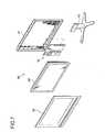
- FIG. 1A description will be given of an embodiment of the configuration of a display device provided with an illumination device according to a preferred embodiment of the present invention, based on FIGS. 1 to 3 .
- a display device 69is illustrated as being horizontally placed with a display surface thereof up.
- the display device 69uses a liquid crystal display panel 59 as a display panel.
- the liquid crystal display panel 59 and a backlight unit 49 that illuminates the liquid crystal display panel 59 from behindare accommodated in a single housing.
- the housingis formed by combining a front housing member HG1 and a rear housing member HG2.
- the liquid crystal display panel 59is formed by fixing an active matrix substrate 51 that includes a switching element such as a thin film transistor (TFT) and a counter substrate 52 that is located opposite to the active matrix substrate 51 to each other with an unillustrated seal member placed therebetween, and filling the space between the active matrix substrate 51 and the counter substrate 52 with liquid crystal.
- a switching elementsuch as a thin film transistor (TFT)
- a counter substrate 52that is located opposite to the active matrix substrate 51 to each other with an unillustrated seal member placed therebetween
- Polarization films 53are fixed one to each of the light receiving side of the active matrix substrate 51 and the light output side of the counter substrate 52.
- the liquid crystal display panel 59forms an image by making use of variation in light transmittance resulting from tilting of liquid crystal molecules.
- the backlight unit 49which embodies the illumination device according to the present invention, has the following configuration. That is, the backlight unit 49 includes light emitting modules MJ, a chassis 41, a reflection seat 42, a large-size diffusion plate 43, a prism seat 44, and microlens sheet 45.
- the light emitting modules MJeach include a mounting board 21, an LED 22 as a light emitting element, a diffusion lens 24, and a built-in reflection sheet 11.
- the illumination device disclosed in Patent Literature 1includes lenses 124 incorporated therein, since light from each of the LEDs 122 is emitted in a small range of directions, a large number of light emitting modules mj need to be arranged in a high density. This increases the cost for preparing and mounting the components, making the illumination device expensive as a whole.
- LEDshave been significantly increased, so that it is now possible to obtain a sufficient amount of light to cover the entire screen with a comparatively small number of LEDs.
- a lens that is highly capable of diffusing lightsuch a lens will herein be referred to as "diffusion lens" in combination with each LED.
- FIG. 9is a graph showing how illuminance (unit: Lux) differs in different irradiation directions in a case of a bare LED and in a case of an LED combined with a diffusion lens.
- the illuminanceis highest at an angle of 90°, which is the angle of the optical axis, and sharply decreases farther away from there.
- illuminance of a certain level or highercan be secured in a wider area, and the peak of illuminance can be set at an angle that is different from the angle of the optical axis.
- the pattern of illuminance shown in the figurecan be changed as desired by accordingly designing the diffusion lens.
- FIG. 10conceptually shows how brightness of a plurality of LEDs gathers.
- the solid-line waveformsindicate the brightness of LEDs each combined with a diffusion lens
- the broken-line waveformsindicate the brightness of bare LEDs.
- the horizontal lines among the waveformsindicate widths (full width at half maximum) of the waveforms at brightness of levels half the peak levels.
- each wavecan have a large width, and thus it is easy to generate integrated, collective brightness as flat brightness as shown in the upper part of the figure.
- the waveformseach have a high peak but have a narrow width, and thus it is impossible to avoid generation of waves in the brightness made by gathering the waveforms. Unevenly bright images are not desirable, so it is almost indispensably necessary to adopt the LED combined with a diffusion lens.
- the light emitting module MJis provided with the diffusion lens 24.
- Each of the mounting boards 21have a shape of elongate rectangle, and on its upper surface which is formed as a mount surface 21U, a plurality of electrodes (not shown) are formed to be arranged at predetermined intervals in the length direction.
- the LEDs 22are mounted on the electrodes.
- the mounting board 21functions as a common mounting board for the plurality of LEDs 22. That is, a plurality of units each composed of a LED 22, a diffusion lens 24, and a built-in reflection sheet 11 are arranged at predetermined intervals along the length direction on the mounting board 21 as shown in FIG. 1 .
- the diffusion lens 24is circular in plan, and has a plurality of legs 24a on a lower surface thereof.
- the tips of the legs 24aare bonded to the mount surface 21 U of the mounting board 21 with an adhesive, and thereby the diffusion lens 24 is attached to the mounting board 21.
- the presence of the legs 24agenerates a gap between the mounting board 21 and the diffusion lens 24. An air flow passes through the gap, and the LED 22 is cooled by the air flow.
- an integrally molded light emitting modulein which an LED is embedded in a diffusion lens.
- LED 22Various types of LEDs can be used as the LED 22.
- an LEDthat is formed by combining a red light-emitting LED chip, a blue light-emitting LED chip, and a fluorescent substance that emits green fluorescence on receiving blue light from the blue light-emitting LED chip, the LED generating white light by mixing the red light, the blue light, and the green light emitted by them.
- an LEDthat is formed by combining a red light-emitting LED chip, a green light-emitting LED chip, and a blue light-emitting LED chip, the LED generating white light by mixing the red light, the green light, and the blue light emitted by them.
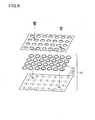
- FIG. 1shows a case where mounting boards 21 each having five LEDs 22 arranged thereon and mounting boards 21 each having eight LEDs 22 arranged thereon are used in combination.
- Each of the mounting boards 21 with five LEDs 22is coupled to any one of the mounting boards 21 with eight LEDs 22 through the connection of connectors 25 which are each attached to one far-end edge of a corresponding one of the mounting boards 21 (it goes without saying that the connectors 25 are separated into male and female connectors).
- a plurality of pairs each composed of one mounting board 21 having five LEDs 22 and one mounting board 21 having eight LEDs 22are arranged on the chassis 41 in parallel with each other.
- the LEDs 22are aligned along the longer-side direction of the chassis 41, that is, along the direction indicated by arrow X in FIG. 1
- the pairs each composed of two mounting boards 21are aligned along the shorter-side direction of the chassis 41, that is, along the direction indicated by arrow Y in FIG. 1 , as a result of which the LEDs 22 are arranged to form a matrix.
- the mounting boards 21are fixed to the chassis 41 by appropriate means such as swaging, bonding, screwing, or riveting.
- the built-in reflection sheet 11is disposed between the mounting board 21 and the diffusion lens 24.
- the built-in reflection sheet 11is fixed to the mount surface 21 U at a position that faces the bottom surface of the diffusion lens 24.
- the built-in reflection sheet 11has a higher optical reflectance than the mounting board 21.
- the built-in reflection sheet 11is also circular in plan and concentric with the diffusion lens 24. In diameter, the built-in reflection sheet 11 is larger than the diffusion lens 24.
- the built-in reflection sheet 11which is a resin foam sheet containing a large number of fine air bubbles, exploits the interface reflection in the air bubbles to the full and has a high optical reflectance.
- Polyethylene-terephthalate (PET) foam sheets having a reflectance of 98% or moreare available, and thus, it is desirable to adopt such a sheet.
- PETpolyethylene-terephthalate
- a reflection sheet 42which is similar to the chassis 41 in plan, is superposed.
- the reflection sheet 42is also a resin foam sheet similar to the built-in reflection sheet 11.
- apertures 42H1each having a shape of a circle that is sized such that the diffusion lens 24 can pass therethrough while the built-in reflection sheet 11 cannot.
- apertures 42H2there are formed rectangular apertures 42H2 for the connectors 25 to protrude therethrough.
- the connectors 25, which electrically connect the mounting boards 21 to each otherare placed in a state in which they do not interfere with the irradiation light region in which the LEDs 22 impart brightness to the diffusion plate 43.
- LEDs 22emit fractional light in the horizontal direction or a substantially horizontal direction as well, but such light is not expected to impart brightness to the diffusion plate 43 and is also weak, and thus is ignorable.
- the irradiation light region in this caseis substantially the light area that is able to function as a backlight.
- the diffusion lenses 24covers the LEDs 22, light from the diffusion lenses 24 forms the irradiation light region.
- the following shapeis imparted to the connectors 25. That is, among edges of the connectors 25, at least one located on the side that faces an LED 22 is formed to be away from the LED 22.
- the connectors 25are denoted with an additional letter A.
- beveled parts 26are formed at edges thereof, to thereby achieve an effect of keeping the edges away from the LEDs 22.
- the connectors 25ASince the connectors 25A have their edges beveled into the beveled parts 26, the connectors 25A are placed in a state in which they do not interfere with the irradiation light region in which the LEDs 22 impart brightness to the diffusion plate 43. As a result, uneven brightness attributable to the connectors 25A is not observed in the diffusion plate 43, and the quality of images displayed on the liquid crystal display panel 59 is improved.
- the size and the inclination angle of the beveled part 26are so set as to help achieve the object of placing the edges of the connectors 25A in a state in which they do not interfere with the irradiation light region in which the LEDs 22 impart brightness to the diffusion plate 43.
- each of the connectors 25Athree of the four sides of the top surface are each formed into the beveled part 26, that is, excluding one side at which the connector 25A contacts the counter connector 25A.
- the beveled part 26it is possible, in each of the connectors 25A, to form the beveled part 26 solely at the side that faces the nearest light emitting module MJ, with no beveled part 26 formed at either of the other two sides that are perpendicular to this side, that is, in FIG. 3 , the upper and lower sides.
- FIG. 4shows a second embodiment of the illumination device.
- the second embodimentis different from the first embodiment in connector shape. That is, each of connectors 25B used in the second embodiment is formed such that a rounded part 27, not a beveled part, is formed at an edge thereof that is located on a side that faces an LED 22.
- the rounded part 27is also effective in keeping edges away from the LEDs 22.
- the connectors 25Bare placed in a state in which they do not interfere with the irradiation light region in which the LEDs 22 impart brightness to the diffusion plate 43.
- uneven brightness attributable to the connectors 25Bis not observed in the diffusion plate 43, and the quality of images displayed on a liquid crystal display panel 59 is improved.
- the size of the rounded part 27is so set as to help achieve the object of placing the edges of the connector 25B in a state in which they do not interfere with the irradiation light region in which the LEDs 22 impart brightness to the diffusion plate 43.
- each of the connectors 25Bthree of the four sides of the top surface may each be formed into the rounded part 27, that is, excluding one side at which the connector 25B contacts the counter connector 25B, or it is possible to form the rounded part 27 solely at the side that faces the nearest light emitting module MJ.
- FIG. 5shows a third embodiment of the illumination device.
- the third embodimentis different from the first and second embodiments in connector shape. That is, each of connectors 25C used in the third embodiment is formed such that a stepped part 28 is formed at an edge thereof that is located on a side that faces an LED 22. There is no particular limitation to the number of steps of which the stepped part 28 is formed.
- the stepped part 28is also effective in keeping edges away from the LEDs 22.
- the connectors 25Care placed in a state in which they do not interfere with the irradiation light region in which the LEDs 22 impart brightness to the diffusion plate 43.
- uneven brightness attributable to the connectors 25Cis not observed in the diffusion plate 43, and the quality of images displayed on a liquid crystal display panel 59 is improved.
- the size and the inclination angle of the stepped part 28are so set as to help achieve the object of placing the edges of the connectors 25C in a state in which they do not interfere with the irradiation light region in which the LEDs 22 impart brightness to the diffusion plate 43.
- each of the connectors 25Cmay each be formed into the stepped part 28, that is, excluding one side at which the connector 25C contacts the counter connector 25C, or it is possible to form the stepped part 28 solely at the side that faces the nearest light emitting module MJ.
- FIG. 6shows a reference example of the illumination device.
- the approach taken in this exampleis different from those taken in the first to third embodiments.
- connectorsare formed with a reduced height to thereby shape them such that they do not interfere with an irradiation light region in which LEDs 22 impart brightness to a diffusion plate 43.
- the connectors 25D shown in FIG. 6are formed such that the height thereof itself is shorter than the maximum heights of the connectors of the first to third embodiments, and thus, the connectors 25D are placed in a state in which they do not interfere with the irradiation light region in which the LEDs 22 impart brightness to the diffusion plate 43. As a result, uneven brightness attributable to the connectors 25D is not observed in the diffusion plate 43, and the quality of images displayed on a liquid crystal display panel 59 is improved.
- FIG. 7shows an example of the configuration of a television receiver in which a display device 69 is incorporated.
- a television receiver 89is configured such that the display device 69 and a group of control boards 92 are housed in a cabinet composed of a front cabinet 90 and a rear cabinet 91 which are attached to each other, the cabinet being supported by a stand 93.
- the present inventionmay be carried out in any other manner than specifically described above as embodiments, and many modifications and variations are possible within the scope of the present invention.
- the present inventionis applicable to a connector for connecting mounting boards on which light emitting elements that are not covered with diffusion lenses are arranged.
- the present inventionis widely applicable to illumination devices, display devices including the illumination devices, and television receivers provided with the display devices.
Landscapes
- Physics & Mathematics (AREA)
- Nonlinear Science (AREA)
- Engineering & Computer Science (AREA)
- General Engineering & Computer Science (AREA)
- Mathematical Physics (AREA)
- Chemical & Material Sciences (AREA)
- Crystallography & Structural Chemistry (AREA)
- General Physics & Mathematics (AREA)
- Optics & Photonics (AREA)
- Planar Illumination Modules (AREA)
- Liquid Crystal (AREA)
Description
- The present invention is related to an illumination device, a display device including the illumination device, and a television receiver having the display device.
- Display devices using a display panel such as a liquid crystal display panel, which does not emit light itself, typically incorporate an illumination device that illuminates the display panel from behind. Various types of light sources including cold cathode tubes and light emitting elements are used as the light source of such an illumination device. Examples of such light emitting elements include light emitting diodes (hereinafter referred to as "LEDs"), organic electroluminescence elements, inorganic electroluminescence elements, among which LEDs are used the most commonly today. The light sources of the illumination device disclosed in Patent Literature 1 are also LEDs.
- In the illumination device disclosed in Patent Literature 1, as shown in
FIG. 8 , LEDs 122 are mounted on themounting board 121, and further,lenses 124 each covering a corresponding one of the LEDs 122 are attached to themounting board 121. Themounting board 121, the LED 122, and thelens 124 together form a light emitting module mj. Thelenses 124 are each formed in a shape of a hemisphere dome with even thickness, and transmit light emitted from the LEDs 122 without significant refraction. Thus, if the LEDs 122 face upward as shown inFIG. 8 , a large part of the light proceeds in a direction close to the vertical direction. DE 10 2007 023651 A1 (D1) relates to a lighting arrangement with a light module that has at least one first group of light sources and one second group of light sources that are arranged spaced apart from each other on a flexible circuit board, and with a carrier on which the light module is mounted, and a buffer zone that laterally overlaps with the light module between the first and the second group of light sources. Furthermore, a backlighting device and a display device are disclosed.US 2006/289201 A1 (D2) relates to a backlight assembly and a display device having the backlight assembly where the backlight assembly includes a plurality of light sources for emitting light and a plurality of metal core printed circuit boards on which the light sources are mounted. The metal core printed circuit boards are directly connected to each other in predetermined regions to emit light in a surface direction. A method of assembling the backlight assembly is further provided.US2008/259240 A1 (D3) relates to a reflector member in a backlight assembly which includes a base sheet reflecting a light and a connecting line disposed on a face of the base sheet. An input pad is disposed at a first end portion of the connecting line and receives signals, and an output is disposed at a second end portion of the connecting line and outputs the signals transmitted through the connecting line.- Patent Literature 1:
JP-A- 2008-41546 - Only a
single mounting board 121 is illustrated inFIG. 8 , but a case of illuminating a large area may require a configuration in which a plurality ofmounting boards 121 are connected to each other with connectors. The illumination device ofFIG. 8 is originally designed as a backlight of a liquid crystal display device, and irradiates a diffusion plate with light from a large number of LEDs 122 to give the diffusion plate even brightness; here, if a plurality ofmounting boards 121 are connected to each other with connectors, the connectors may block the light from the LEDs 122 to cast their shadows onto the diffusion plate. - The present invention has been made in view of the foregoing, and an object of the present invention is, with respect to an illumination device that irradiates a diffusion plate with light from a light source built as a combination of a plurality of mounting boards on which light emitting elements are mounted, to prevent connectors used for connecting the mounting boards to each other from causing uneven brightness of the diffusion plate.
- According to the present invention, an illumination device is provided as defined in claim 1.
- With this configuration, light that imparts brightness to the diffusion plate is not blocked by the connectors, and thus the diffusion plate does not suffer from uneven brightness caused by the connectors.
- According to a preferred embodiment of the present invention, the illumination device configured as described above further includes a diffusion lens that covers the light emitting element. Here, light from the diffusion lens forms the irradiation light region.
- With this configuration, the light from the diffusion lens is not blocked by the connectors, and thus the diffusion plate does not suffer from uneven brightness caused by the connectors.
- In the illumination device configured as described above, among edges of the connectors, at least an edge which is located on a side that faces the light emitting element is formed to be away from the light emitting element, to thereby impart to the connectors a shape which allows the connectors to be in a state in which the connectors do not interfere with the irradiation light region.
- With this configuration, it is possible to eliminate unevenness in brightness by changing the shape of the connectors, and thus the object of the present invention is easily achieved.
- According to a preferred embodiment of the present invention, in the illumination device configured as described above, among the edges of the connectors, at least the edge which is located on the side that faces the light emitting element is formed to be away from the light emitting element by forming a beveled part at the edge.
- With this configuration, the shape of the connectors is easily changed simply by forming the beveled part in the connectors.
- According to a preferred embodiment of the present invention, in the illumination device configured as described above, among the edges of the connectors, at least the edge which is located on the side that faces the light emitting element is formed to be away from the light emitting element by forming a rounded part at the edge.
- With this configuration, the shape of the connectors is easily changed simply by forming the rounded part in the connectors.
- According to a preferred embodiment of the present invention, in the illumination device configured as described above, among the edges of the connectors, at least the edge which is located on the side that faces the light emitting element is formed to be away from the light emitting element by forming a stepped part at the edge.
- With this configuration, the shape of the connectors is easily changed simply by forming the stepped part in the connectors.
- According to a preferred embodiment of the present invention, in the illumination device configured as described above, the light emitting element is an LED.
- With this configuration, it is possible to obtain a bright illumination device by using LEDs brightness of which has recently been remarkably increased.
- According to a preferred embodiment of the present invention, a display device includes: any illumination device of the illumination devices configured as described above; and a display panel which receives light from the illumination device.
- With this configuration, it is possible to obtain a display device free from brightness unevenness stemming from the connectors.
- According to a preferred embodiment of the present invention, in the display device configured as described above, the display panel is a liquid crystal display panel.
- With this configuration, it is possible to obtain a liquid crystal display device free from brightness unevenness stemming from the connectors.
- According to a preferred embodiment of the present invention, a television receiver includes the display device configured as described above.
- With this configuration, it is possible to obtain a television receiver in which the screen is free from brightness unevenness stemming from the connectors.
- According to the present invention, light from the light emitting element that imparts brightness to the diffusion plate is not blocked by the connectors, and thus the connectors do not cause uneven brightness, and this helps improve the quality of images displayed on the display device incorporating the display panel that receives light from the illumination device of the present invention. This further helps improve the image quality of the television receiver incorporating the display device.
- [
FIG. 1 ] An exploded perspective view showing a display device including an illumination device according to a preferred embodiment of the present invention; - [
FIG. 2 ] A sectional view showing a mounting-board joint portion of the illumination device according to a first embodiment; - [
FIG. 3 ] A plan view showing the mounting-board joint portion ofFIG. 2 ; - [
FIG. 4 ] A sectional view showing a mounting-board joint portion of an illumination device according to a second embodiment; - [
FIG. 5 ] A sectional view showing a mounting-board joint portion of an illumination device according to a third embodiment; - [
FIG. 6 ] A sectional view showing a mounting-board joint portion of an illumination device according to a reference example; - [
FIG. 7 ] An exploded perspective view showing a television receiver; - [
FIG. 8 ] An exploded perspective view showing a conventional illumination device; - [
FIG. 9 ] A graph showing how illuminance differs in different directions of irradiation from an LED; and - [
FIG. 10 ] A conceptual diagram showing how brightness of a plurality of LEDs gathers. - A description will be given of an embodiment of the configuration of a display device provided with an illumination device according to a preferred embodiment of the present invention, based on
FIGS. 1 to 3 . InFIG. 1 , adisplay device 69 is illustrated as being horizontally placed with a display surface thereof up. - The
display device 69 uses a liquidcrystal display panel 59 as a display panel. The liquidcrystal display panel 59 and abacklight unit 49 that illuminates the liquidcrystal display panel 59 from behind are accommodated in a single housing. The housing is formed by combining a front housing member HG1 and a rear housing member HG2. - The liquid
crystal display panel 59 is formed by fixing anactive matrix substrate 51 that includes a switching element such as a thin film transistor (TFT) and acounter substrate 52 that is located opposite to theactive matrix substrate 51 to each other with an unillustrated seal member placed therebetween, and filling the space between theactive matrix substrate 51 and thecounter substrate 52 with liquid crystal. Polarization films 53 are fixed one to each of the light receiving side of theactive matrix substrate 51 and the light output side of thecounter substrate 52. The liquidcrystal display panel 59 forms an image by making use of variation in light transmittance resulting from tilting of liquid crystal molecules.- The
backlight unit 49, which embodies the illumination device according to the present invention, has the following configuration. That is, thebacklight unit 49 includes light emitting modules MJ, achassis 41, areflection seat 42, a large-size diffusion plate 43, aprism seat 44, andmicrolens sheet 45. - The light emitting modules MJ each include a mounting
board 21, anLED 22 as a light emitting element, adiffusion lens 24, and a built-inreflection sheet 11. - Now, a description will be given of the importance of the
diffusion lens 24. Take, for example, the illumination device disclosed in Patent Literature 1. Although the illumination device shown inFIG. 8 includeslenses 124 incorporated therein, since light from each of the LEDs 122 is emitted in a small range of directions, a large number of light emitting modules mj need to be arranged in a high density. This increases the cost for preparing and mounting the components, making the illumination device expensive as a whole. - Recently, the brightness of LEDs has been significantly increased, so that it is now possible to obtain a sufficient amount of light to cover the entire screen with a comparatively small number of LEDs. However, if a small number of high-brightness LEDs are sparsely arranged, it is impossible to prevent uneven brightness, and thus, it is preferable to use a lens that is highly capable of diffusing light (such a lens will herein be referred to as "diffusion lens") in combination with each LED.
FIG. 9 is a graph showing how illuminance (unit: Lux) differs in different irradiation directions in a case of a bare LED and in a case of an LED combined with a diffusion lens. In the case of the bare LED, the illuminance is highest at an angle of 90°, which is the angle of the optical axis, and sharply decreases farther away from there. In contrast, in the case of the LED combined with a diffusion lens, illuminance of a certain level or higher can be secured in a wider area, and the peak of illuminance can be set at an angle that is different from the angle of the optical axis. Needless to say, the pattern of illuminance shown in the figure can be changed as desired by accordingly designing the diffusion lens.FIG. 10 conceptually shows how brightness of a plurality of LEDs gathers. In the figure, the solid-line waveforms indicate the brightness of LEDs each combined with a diffusion lens, while the broken-line waveforms indicate the brightness of bare LEDs. The horizontal lines among the waveforms indicate widths (full width at half maximum) of the waveforms at brightness of levels half the peak levels. In the case of the LEDs each combined with a diffusion lens, each wave can have a large width, and thus it is easy to generate integrated, collective brightness as flat brightness as shown in the upper part of the figure. In contrast, in the case of the bare LEDs, the waveforms each have a high peak but have a narrow width, and thus it is impossible to avoid generation of waves in the brightness made by gathering the waveforms. Unevenly bright images are not desirable, so it is almost indispensably necessary to adopt the LED combined with a diffusion lens.- In view of the above, the light emitting module MJ is provided with the
diffusion lens 24. - Each of the mounting
boards 21 have a shape of elongate rectangle, and on its upper surface which is formed as amount surface 21U, a plurality of electrodes (not shown) are formed to be arranged at predetermined intervals in the length direction. TheLEDs 22 are mounted on the electrodes. The mountingboard 21 functions as a common mounting board for the plurality ofLEDs 22. That is, a plurality of units each composed of aLED 22, adiffusion lens 24, and a built-inreflection sheet 11 are arranged at predetermined intervals along the length direction on the mountingboard 21 as shown inFIG. 1 . - The
diffusion lens 24 is circular in plan, and has a plurality oflegs 24a on a lower surface thereof. The tips of thelegs 24a are bonded to themount surface 21 U of the mountingboard 21 with an adhesive, and thereby thediffusion lens 24 is attached to the mountingboard 21. The presence of thelegs 24a generates a gap between the mountingboard 21 and thediffusion lens 24. An air flow passes through the gap, and theLED 22 is cooled by the air flow. Incidentally, on the condition that heat dissipation is secured, it is possible to use an integrally molded light emitting module in which an LED is embedded in a diffusion lens. - Various types of LEDs can be used as the
LED 22. For example, it is possible to use an LED that is formed by combining a blue light-emitting LED chip with a fluorescent substance that emits yellow fluorescence on receiving light from the LED chip, the LED generating white light by mixing the blue light and the yellow light emitted by them. It is also possible to use an LED that is formed by combining a blue light-emitting LED chip with fluorescent substances that respectively emit green fluorescence and red fluorescence on receiving light from the LED chip, the LED generating white light by mixing the blue light, the green light, and the red light emitted by them. - It is also possible to use an LED that is formed by combining a red light-emitting LED chip, a blue light-emitting LED chip, and a fluorescent substance that emits green fluorescence on receiving blue light from the blue light-emitting LED chip, the LED generating white light by mixing the red light, the blue light, and the green light emitted by them.
- It is also possible to use an LED that is formed by combining a red light-emitting LED chip, a green light-emitting LED chip, and a blue light-emitting LED chip, the LED generating white light by mixing the red light, the green light, and the blue light emitted by them.
FIG. 1 shows a case where mountingboards 21 each having fiveLEDs 22 arranged thereon and mountingboards 21 each having eightLEDs 22 arranged thereon are used in combination. Each of the mountingboards 21 with fiveLEDs 22 is coupled to any one of the mountingboards 21 with eightLEDs 22 through the connection ofconnectors 25 which are each attached to one far-end edge of a corresponding one of the mounting boards 21 (it goes without saying that theconnectors 25 are separated into male and female connectors).- A plurality of pairs each composed of one mounting
board 21 having fiveLEDs 22 and one mountingboard 21 having eightLEDs 22 are arranged on thechassis 41 in parallel with each other. On each of the mountingboards 21, theLEDs 22 are aligned along the longer-side direction of thechassis 41, that is, along the direction indicated by arrow X inFIG. 1 , and the pairs each composed of two mountingboards 21 are aligned along the shorter-side direction of thechassis 41, that is, along the direction indicated by arrow Y inFIG. 1 , as a result of which theLEDs 22 are arranged to form a matrix. The mountingboards 21 are fixed to thechassis 41 by appropriate means such as swaging, bonding, screwing, or riveting. - The built-in
reflection sheet 11 is disposed between the mountingboard 21 and thediffusion lens 24. The built-inreflection sheet 11 is fixed to themount surface 21 U at a position that faces the bottom surface of thediffusion lens 24. The built-inreflection sheet 11 has a higher optical reflectance than the mountingboard 21. The built-inreflection sheet 11 is also circular in plan and concentric with thediffusion lens 24. In diameter, the built-inreflection sheet 11 is larger than thediffusion lens 24. - The built-in
reflection sheet 11, which is a resin foam sheet containing a large number of fine air bubbles, exploits the interface reflection in the air bubbles to the full and has a high optical reflectance. Polyethylene-terephthalate (PET) foam sheets having a reflectance of 98% or more are available, and thus, it is desirable to adopt such a sheet. In the built-inreflection sheet 11, there are formed through holes through which thelegs 24a of thediffusion lens 24 are inserted. Incidentally, inFIG. 3 , illustration of the built-inreflection sheet 11 is omitted. - On the
chassis 41, areflection sheet 42, which is similar to thechassis 41 in plan, is superposed. Thereflection sheet 42 is also a resin foam sheet similar to the built-inreflection sheet 11. In thereflection sheet 42, corresponding to the positions of the light emitting modules MJ, there are formed apertures 42H1 each having a shape of a circle that is sized such that thediffusion lens 24 can pass therethrough while the built-inreflection sheet 11 cannot. Further, in thereflection sheet 42, corresponding to the positions of theconnectors 25, there are formed rectangular apertures 42H2 for theconnectors 25 to protrude therethrough. - In the
backlight unit 49, theconnectors 25, which electrically connect the mountingboards 21 to each other are placed in a state in which they do not interfere with the irradiation light region in which theLEDs 22 impart brightness to thediffusion plate 43.LEDs 22 emit fractional light in the horizontal direction or a substantially horizontal direction as well, but such light is not expected to impart brightness to thediffusion plate 43 and is also weak, and thus is ignorable. It is assumed that the irradiation light region in this case is substantially the light area that is able to function as a backlight. Here, since thediffusion lenses 24 covers theLEDs 22, light from thediffusion lenses 24 forms the irradiation light region. - For the purpose of securely placing the
connectors 25 in a state in which they do not interfere with the irradiation light region in which theLEDs 22 impart brightness to thediffusion plate 43, the following shape is imparted to theconnectors 25. That is, among edges of theconnectors 25, at least one located on the side that faces anLED 22 is formed to be away from theLED 22. - In the illumination device of the first embodiment shown in
FIG. 2 and FIG. 3 , theconnectors 25 are denoted with an additional letter A. In theconnectors 25A, beveledparts 26 are formed at edges thereof, to thereby achieve an effect of keeping the edges away from theLEDs 22. - Since the
connectors 25A have their edges beveled into thebeveled parts 26, theconnectors 25A are placed in a state in which they do not interfere with the irradiation light region in which theLEDs 22 impart brightness to thediffusion plate 43. As a result, uneven brightness attributable to theconnectors 25A is not observed in thediffusion plate 43, and the quality of images displayed on the liquidcrystal display panel 59 is improved. The size and the inclination angle of thebeveled part 26 are so set as to help achieve the object of placing the edges of theconnectors 25A in a state in which they do not interfere with the irradiation light region in which theLEDs 22 impart brightness to thediffusion plate 43. - As shown in
FIG. 3 , in each of theconnectors 25A, three of the four sides of the top surface are each formed into thebeveled part 26, that is, excluding one side at which theconnector 25A contacts thecounter connector 25A. However, depending on the positional relationship between the matrix of the light emitting modules MJ and theconnectors 25A, it is possible, in each of theconnectors 25A, to form thebeveled part 26 solely at the side that faces the nearest light emitting module MJ, with nobeveled part 26 formed at either of the other two sides that are perpendicular to this side, that is, inFIG. 3 , the upper and lower sides. FIG. 4 shows a second embodiment of the illumination device. The second embodiment is different from the first embodiment in connector shape. That is, each ofconnectors 25B used in the second embodiment is formed such that arounded part 27, not a beveled part, is formed at an edge thereof that is located on a side that faces anLED 22.- The
rounded part 27 is also effective in keeping edges away from theLEDs 22. Thus, theconnectors 25B are placed in a state in which they do not interfere with the irradiation light region in which theLEDs 22 impart brightness to thediffusion plate 43. As a result, uneven brightness attributable to theconnectors 25B is not observed in thediffusion plate 43, and the quality of images displayed on a liquidcrystal display panel 59 is improved. The size of therounded part 27 is so set as to help achieve the object of placing the edges of theconnector 25B in a state in which they do not interfere with the irradiation light region in which theLEDs 22 impart brightness to thediffusion plate 43. - Like the
beveled part 26 of the first embodiment, in each of theconnectors 25B, three of the four sides of the top surface may each be formed into therounded part 27, that is, excluding one side at which theconnector 25B contacts thecounter connector 25B, or it is possible to form therounded part 27 solely at the side that faces the nearest light emitting module MJ. FIG. 5 shows a third embodiment of the illumination device. The third embodiment is different from the first and second embodiments in connector shape. That is, each ofconnectors 25C used in the third embodiment is formed such that a steppedpart 28 is formed at an edge thereof that is located on a side that faces anLED 22. There is no particular limitation to the number of steps of which the steppedpart 28 is formed.- The stepped
part 28 is also effective in keeping edges away from theLEDs 22. Thus, theconnectors 25C are placed in a state in which they do not interfere with the irradiation light region in which theLEDs 22 impart brightness to thediffusion plate 43. As a result, uneven brightness attributable to theconnectors 25C is not observed in thediffusion plate 43, and the quality of images displayed on a liquidcrystal display panel 59 is improved. The size and the inclination angle of the steppedpart 28 are so set as to help achieve the object of placing the edges of theconnectors 25C in a state in which they do not interfere with the irradiation light region in which theLEDs 22 impart brightness to thediffusion plate 43. - In this case as well, like in the cases of the
beveled part 26 and therounded part 27, three of the four sides of the top surface of each of theconnectors 25C may each be formed into the steppedpart 28, that is, excluding one side at which theconnector 25C contacts thecounter connector 25C, or it is possible to form the steppedpart 28 solely at the side that faces the nearest light emitting module MJ. FIG. 6 shows a reference example of the illumination device. The approach taken in this example is different from those taken in the first to third embodiments. Specifically, in this example, connectors are formed with a reduced height to thereby shape them such that they do not interfere with an irradiation light region in whichLEDs 22 impart brightness to adiffusion plate 43.- The
connectors 25D shown inFIG. 6 are formed such that the height thereof itself is shorter than the maximum heights of the connectors of the first to third embodiments, and thus, theconnectors 25D are placed in a state in which they do not interfere with the irradiation light region in which theLEDs 22 impart brightness to thediffusion plate 43. As a result, uneven brightness attributable to theconnectors 25D is not observed in thediffusion plate 43, and the quality of images displayed on a liquidcrystal display panel 59 is improved. FIG. 7 shows an example of the configuration of a television receiver in which adisplay device 69 is incorporated. Atelevision receiver 89 is configured such that thedisplay device 69 and a group ofcontrol boards 92 are housed in a cabinet composed of afront cabinet 90 and arear cabinet 91 which are attached to each other, the cabinet being supported by astand 93.- It is to be understood that the present invention may be carried out in any other manner than specifically described above as embodiments, and many modifications and variations are possible within the scope of the present invention. For example, the present invention is applicable to a connector for connecting mounting boards on which light emitting elements that are not covered with diffusion lenses are arranged.
- The present invention is widely applicable to illumination devices, display devices including the illumination devices, and television receivers provided with the display devices.
- 49
- backlight unit
- 41
- chassis
- 43
- diffusion plate
- MJ
- light emitting module
- 11
- built-in reflection sheet
- 21
- mounting board
- 22
- LED
- 24
- diffusion lens
- 25, 25A, 25B, 25C, 25D
- connector
- 26
- beveled part
- 27
- rounded part
- 28
- stepped part
- 59
- liquid crystal display panel
- 69
- display device
- 89
- television receiver
Claims (6)
- An illumination device (49), comprising:a diffusion plate (43); anda light source which irradiates the diffusion plate (43) with light,whereinthe light source is configured by combining a plurality of mounting boards (21) on each of which a plurality of light emitting elements (22) is mounted;connectors (25) are attached to corresponding edges of the plurality of mounting boards (21) to electrically connect adjacent ones of the mounting boards (21) to each other;whereinamong edges of the connectors (25), at least an edge which is located on a side that faces the nearest one of said light emitting elements (22) is beveled, rounded, or stepped away from said light emitting element (22) such that light that imparts brightness to the diffusion plate (43) is not hindered by the connectors (25).
- The illumination device (49) of claim 1, further comprising:a diffusion lens (24) which covers each light emitting element (22), whereinlight from the diffusion lens (24) forms the irradiation light region.
- The illumination device (49) of claim 1, wherein the light emitting element (22) is an LED.
- A display device (69), comprising:any illumination device (49) of the illumination devices of claims 1 to 3; and a display panel (59) which receives light from the illumination device (49).
- The display device (69) of claim 4, wherein the display panel (59) is a liquid crystal display panel.
- A television receiver (89), comprising: the display device (69) of claim 4.
Applications Claiming Priority (2)
| Application Number | Priority Date | Filing Date | Title |
|---|---|---|---|
| JP2009141741 | 2009-06-15 | ||
| PCT/JP2010/052312WO2010146893A1 (en) | 2009-06-15 | 2010-02-17 | Illumination device, display device, and television receiver |
Publications (3)
| Publication Number | Publication Date |
|---|---|
| EP2428719A1 EP2428719A1 (en) | 2012-03-14 |
| EP2428719A4 EP2428719A4 (en) | 2013-04-24 |
| EP2428719B1true EP2428719B1 (en) | 2016-01-13 |
Family
ID=43356223
Family Applications (1)
| Application Number | Title | Priority Date | Filing Date |
|---|---|---|---|
| EP10789271.3ANot-in-forceEP2428719B1 (en) | 2009-06-15 | 2010-02-17 | Illumination device, display device, and television receiver |
Country Status (7)
| Country | Link |
|---|---|
| US (1) | US8789960B2 (en) |
| EP (1) | EP2428719B1 (en) |
| JP (1) | JP5138812B2 (en) |
| CN (1) | CN102428312A (en) |
| BR (1) | BR112012000542A2 (en) |
| RU (1) | RU2497040C2 (en) |
| WO (1) | WO2010146893A1 (en) |
Families Citing this family (7)
| Publication number | Priority date | Publication date | Assignee | Title |
|---|---|---|---|---|
| WO2014087278A1 (en) | 2012-12-03 | 2014-06-12 | Koninklijke Philips N.V. | Light emitting arrangement using light guides. |
| KR102203950B1 (en)* | 2014-02-05 | 2021-01-19 | 삼성디스플레이 주식회사 | Light source module, backlight assembly including the same, and display device including the light source module |
| CN104456187A (en)* | 2014-11-13 | 2015-03-25 | 惠州市华瑞光源科技有限公司 | Backlight module and obtained liquid crystal display television |
| CN106151888B (en)* | 2015-05-11 | 2021-03-02 | 松下知识产权经营株式会社 | Light source unit and lighting fixture including the same |
| CN110738937B (en)* | 2018-07-20 | 2021-12-07 | 英属开曼群岛商镎创科技股份有限公司 | Display panel |
| USD925110S1 (en)* | 2019-10-01 | 2021-07-13 | Vince DUNDEE | LED display ceiling mount |
| CN115691308B (en)* | 2021-07-22 | 2025-09-30 | 瑞仪光电(南京)有限公司 | Backlight module and display device |
Family Cites Families (23)
| Publication number | Priority date | Publication date | Assignee | Title |
|---|---|---|---|---|
| US6543911B1 (en)* | 2000-05-08 | 2003-04-08 | Farlight Llc | Highly efficient luminaire having optical transformer providing precalculated angular intensity distribution and method therefore |
| RU2235942C2 (en)* | 2001-12-29 | 2004-09-10 | Басов Юрий Георгиевич | Dome light exploiting light-emitting diodes |
| DE10361116B4 (en)* | 2003-12-22 | 2010-06-17 | Auer Lighting Gmbh | Fresnels |
| RU2267053C2 (en)* | 2004-03-16 | 2005-12-27 | Марков Валерий Николаевич | Universal light-emitting diode lamp |
| JP2005339881A (en)* | 2004-05-25 | 2005-12-08 | Hitachi Displays Ltd | Lighting device, lighting module, and liquid crystal display device |
| KR101157233B1 (en)* | 2004-10-30 | 2012-06-15 | 엘지디스플레이 주식회사 | Apparatus of light emitting diode backlight and liquid crystal display device using thereof |
| KR20060134375A (en)* | 2005-06-22 | 2006-12-28 | 삼성전자주식회사 | Back light assembly and display device having same |
| KR20070006458A (en)* | 2005-07-08 | 2007-01-11 | 삼성전자주식회사 | Light emitting diode module, backlight assembly having same, and display device having same |
| KR101212137B1 (en)* | 2005-08-05 | 2012-12-14 | 엘지디스플레이 주식회사 | backlight unit |
| US7621655B2 (en)* | 2005-11-18 | 2009-11-24 | Cree, Inc. | LED lighting units and assemblies with edge connectors |
| JP5166278B2 (en)* | 2005-11-18 | 2013-03-21 | クリー インコーポレイテッド | Solid-state lighting tile |
| KR100755615B1 (en)* | 2006-04-14 | 2007-09-06 | 삼성전기주식회사 | Backlight of liquid crystal display using light emitting diode |
| KR101239823B1 (en)* | 2006-06-26 | 2013-03-06 | 엘지디스플레이 주식회사 | Backlight unit for Liquid Crystal Display device using thereof |
| KR20080013592A (en)* | 2006-08-09 | 2008-02-13 | 삼성전자주식회사 | Backlight unit and display device including same |
| JP4533352B2 (en) | 2006-08-09 | 2010-09-01 | 昭和電工株式会社 | Light emitting device, display device, and cover mounting member |
| KR101277750B1 (en) | 2006-10-19 | 2013-06-24 | 삼성디스플레이 주식회사 | Reflector member, backlight assembly and dislplay apparatus having the same |
| JP4743104B2 (en)* | 2006-12-13 | 2011-08-10 | ソニー株式会社 | Backlight device and liquid crystal display device |
| DE102007023651A1 (en) | 2007-05-22 | 2008-11-27 | Osram Gesellschaft mit beschränkter Haftung | Lighting device, backlight device and display device |
| JP2009076456A (en)* | 2007-08-31 | 2009-04-09 | Sharp Corp | Backlight device and display device |
| CN101408291A (en)* | 2007-10-11 | 2009-04-15 | 富士迈半导体精密工业(上海)有限公司 | Light source module group and corresponding light source device |
| KR101535926B1 (en)* | 2008-08-12 | 2015-07-13 | 삼성디스플레이 주식회사 | Light emitting diode backlight assembly and liquid crystal display thereof |
| KR101359674B1 (en)* | 2008-08-14 | 2014-02-07 | 삼성전자주식회사 | Planar light source and backlight unit comprising the same |
| TW201018822A (en)* | 2008-11-10 | 2010-05-16 | Everlight Electronics Co Ltd | Illumination device and light emitting diode module |
- 2010
- 2010-02-17EPEP10789271.3Apatent/EP2428719B1/ennot_activeNot-in-force
- 2010-02-17RURU2012101238/07Apatent/RU2497040C2/ennot_activeIP Right Cessation
- 2010-02-17USUS13/320,781patent/US8789960B2/enactiveActive
- 2010-02-17JPJP2011519624Apatent/JP5138812B2/ennot_activeExpired - Fee Related
- 2010-02-17WOPCT/JP2010/052312patent/WO2010146893A1/enactiveApplication Filing
- 2010-02-17BRBR112012000542Apatent/BR112012000542A2/ennot_activeIP Right Cessation
- 2010-02-17CNCN2010800216129Apatent/CN102428312A/enactivePending
Also Published As
| Publication number | Publication date |
|---|---|
| BR112012000542A2 (en) | 2019-09-24 |
| WO2010146893A1 (en) | 2010-12-23 |
| US8789960B2 (en) | 2014-07-29 |
| RU2497040C2 (en) | 2013-10-27 |
| US20120074440A1 (en) | 2012-03-29 |
| EP2428719A4 (en) | 2013-04-24 |
| JP5138812B2 (en) | 2013-02-06 |
| CN102428312A (en) | 2012-04-25 |
| RU2012101238A (en) | 2013-07-27 |
| EP2428719A1 (en) | 2012-03-14 |
| JPWO2010146893A1 (en) | 2012-12-06 |
Similar Documents
| Publication | Publication Date | Title |
|---|---|---|
| RU2496050C2 (en) | Lighting device, display device and television receiver | |
| US8827478B2 (en) | Lighting device, display device, and television receiver | |
| RU2491472C1 (en) | Illumination device and display device | |
| JP5198662B2 (en) | LIGHTING DEVICE, DISPLAY DEVICE, AND TELEVISION RECEIVER | |
| EP2428719B1 (en) | Illumination device, display device, and television receiver | |
| KR20100078296A (en) | Liquid crystal display device module | |
| WO2010146894A1 (en) | Light emitting module, illuminating device, display device, and television receiver | |
| US20120236213A1 (en) | Lighting device, display device and television receiver | |
| CN108508652B (en) | display device | |
| KR20090043799A (en) | LCD Display Module | |
| KR20160022420A (en) | Display device | |
| RU2500951C2 (en) | Lighting unit, display device and tv receiver | |
| RU2499183C2 (en) | Backlighting device, display device and tv set | |
| US8657458B2 (en) | Lighting device, display device and television receiver | |
| JP2013157173A (en) | Lighting device and display device | |
| KR101920760B1 (en) | Liquid crystal display module inculding backlight unit | |
| KR101785340B1 (en) | cover bottom and liquid crystal display device module including the same | |
| KR20160002569A (en) | liquid crystal display device | |
| KR20160012577A (en) | Back light having light emitting device array | |
| KR101681781B1 (en) | Liquid crystal display device | |
| KR20140139817A (en) | Light emitting diode and liquid crystal display device having the same | |
| KR20160094163A (en) | Liquid crystal display device |
Legal Events
| Date | Code | Title | Description |
|---|---|---|---|
| PUAI | Public reference made under article 153(3) epc to a published international application that has entered the european phase | Free format text:ORIGINAL CODE: 0009012 | |
| 17P | Request for examination filed | Effective date:20111208 | |
| AK | Designated contracting states | Kind code of ref document:A1 Designated state(s):AT BE BG CH CY CZ DE DK EE ES FI FR GB GR HR HU IE IS IT LI LT LU LV MC MK MT NL NO PL PT RO SE SI SK SM TR | |
| DAX | Request for extension of the european patent (deleted) | ||
| A4 | Supplementary search report drawn up and despatched | Effective date:20130326 | |
| RIC1 | Information provided on ipc code assigned before grant | Ipc:F21V 23/06 20060101ALI20130320BHEP Ipc:F21Y 101/02 20060101ALI20130320BHEP Ipc:G02F 1/13357 20060101ALI20130320BHEP Ipc:F21S 2/00 20060101AFI20130320BHEP | |
| GRAP | Despatch of communication of intention to grant a patent | Free format text:ORIGINAL CODE: EPIDOSNIGR1 | |
| INTG | Intention to grant announced | Effective date:20150813 | |
| GRAS | Grant fee paid | Free format text:ORIGINAL CODE: EPIDOSNIGR3 | |
| GRAA | (expected) grant | Free format text:ORIGINAL CODE: 0009210 | |
| AK | Designated contracting states | Kind code of ref document:B1 Designated state(s):AT BE BG CH CY CZ DE DK EE ES FI FR GB GR HR HU IE IS IT LI LT LU LV MC MK MT NL NO PL PT RO SE SI SK SM TR | |
| REG | Reference to a national code | Ref country code:GB Ref legal event code:FG4D | |
| REG | Reference to a national code | Ref country code:CH Ref legal event code:EP | |
| REG | Reference to a national code | Ref country code:IE Ref legal event code:FG4D | |
| REG | Reference to a national code | Ref country code:AT Ref legal event code:REF Ref document number:770765 Country of ref document:AT Kind code of ref document:T Effective date:20160215 | |
| REG | Reference to a national code | Ref country code:DE Ref legal event code:R096 Ref document number:602010030211 Country of ref document:DE | |
| REG | Reference to a national code | Ref country code:NL Ref legal event code:FP | |
| PGFP | Annual fee paid to national office [announced via postgrant information from national office to epo] | Ref country code:DE Payment date:20160218 Year of fee payment:7 | |
| REG | Reference to a national code | Ref country code:LT Ref legal event code:MG4D | |
| PG25 | Lapsed in a contracting state [announced via postgrant information from national office to epo] | Ref country code:BE Free format text:LAPSE BECAUSE OF NON-PAYMENT OF DUE FEES Effective date:20160229 | |
| PGFP | Annual fee paid to national office [announced via postgrant information from national office to epo] | Ref country code:GB Payment date:20160217 Year of fee payment:7 Ref country code:NL Payment date:20160217 Year of fee payment:7 | |
| REG | Reference to a national code | Ref country code:AT Ref legal event code:MK05 Ref document number:770765 Country of ref document:AT Kind code of ref document:T Effective date:20160113 | |
| PG25 | Lapsed in a contracting state [announced via postgrant information from national office to epo] | Ref country code:GR Free format text:LAPSE BECAUSE OF FAILURE TO SUBMIT A TRANSLATION OF THE DESCRIPTION OR TO PAY THE FEE WITHIN THE PRESCRIBED TIME-LIMIT Effective date:20160414 Ref country code:FI Free format text:LAPSE BECAUSE OF FAILURE TO SUBMIT A TRANSLATION OF THE DESCRIPTION OR TO PAY THE FEE WITHIN THE PRESCRIBED TIME-LIMIT Effective date:20160113 Ref country code:IT Free format text:LAPSE BECAUSE OF FAILURE TO SUBMIT A TRANSLATION OF THE DESCRIPTION OR TO PAY THE FEE WITHIN THE PRESCRIBED TIME-LIMIT Effective date:20160113 Ref country code:HR Free format text:LAPSE BECAUSE OF FAILURE TO SUBMIT A TRANSLATION OF THE DESCRIPTION OR TO PAY THE FEE WITHIN THE PRESCRIBED TIME-LIMIT Effective date:20160113 Ref country code:NO Free format text:LAPSE BECAUSE OF FAILURE TO SUBMIT A TRANSLATION OF THE DESCRIPTION OR TO PAY THE FEE WITHIN THE PRESCRIBED TIME-LIMIT Effective date:20160413 Ref country code:ES Free format text:LAPSE BECAUSE OF FAILURE TO SUBMIT A TRANSLATION OF THE DESCRIPTION OR TO PAY THE FEE WITHIN THE PRESCRIBED TIME-LIMIT Effective date:20160113 | |
| PG25 | Lapsed in a contracting state [announced via postgrant information from national office to epo] | Ref country code:SE Free format text:LAPSE BECAUSE OF FAILURE TO SUBMIT A TRANSLATION OF THE DESCRIPTION OR TO PAY THE FEE WITHIN THE PRESCRIBED TIME-LIMIT Effective date:20160113 Ref country code:LV Free format text:LAPSE BECAUSE OF FAILURE TO SUBMIT A TRANSLATION OF THE DESCRIPTION OR TO PAY THE FEE WITHIN THE PRESCRIBED TIME-LIMIT Effective date:20160113 Ref country code:LT Free format text:LAPSE BECAUSE OF FAILURE TO SUBMIT A TRANSLATION OF THE DESCRIPTION OR TO PAY THE FEE WITHIN THE PRESCRIBED TIME-LIMIT Effective date:20160113 Ref country code:IS Free format text:LAPSE BECAUSE OF FAILURE TO SUBMIT A TRANSLATION OF THE DESCRIPTION OR TO PAY THE FEE WITHIN THE PRESCRIBED TIME-LIMIT Effective date:20160513 Ref country code:PT Free format text:LAPSE BECAUSE OF FAILURE TO SUBMIT A TRANSLATION OF THE DESCRIPTION OR TO PAY THE FEE WITHIN THE PRESCRIBED TIME-LIMIT Effective date:20160513 Ref country code:PL Free format text:LAPSE BECAUSE OF FAILURE TO SUBMIT A TRANSLATION OF THE DESCRIPTION OR TO PAY THE FEE WITHIN THE PRESCRIBED TIME-LIMIT Effective date:20160113 Ref country code:AT Free format text:LAPSE BECAUSE OF FAILURE TO SUBMIT A TRANSLATION OF THE DESCRIPTION OR TO PAY THE FEE WITHIN THE PRESCRIBED TIME-LIMIT Effective date:20160113 | |
| REG | Reference to a national code | Ref country code:CH Ref legal event code:PL | |
| REG | Reference to a national code | Ref country code:DE Ref legal event code:R097 Ref document number:602010030211 Country of ref document:DE | |
| PG25 | Lapsed in a contracting state [announced via postgrant information from national office to epo] | Ref country code:MC Free format text:LAPSE BECAUSE OF FAILURE TO SUBMIT A TRANSLATION OF THE DESCRIPTION OR TO PAY THE FEE WITHIN THE PRESCRIBED TIME-LIMIT Effective date:20160113 Ref country code:CH Free format text:LAPSE BECAUSE OF NON-PAYMENT OF DUE FEES Effective date:20160229 Ref country code:LI Free format text:LAPSE BECAUSE OF NON-PAYMENT OF DUE FEES Effective date:20160229 Ref country code:EE Free format text:LAPSE BECAUSE OF FAILURE TO SUBMIT A TRANSLATION OF THE DESCRIPTION OR TO PAY THE FEE WITHIN THE PRESCRIBED TIME-LIMIT Effective date:20160113 Ref country code:DK Free format text:LAPSE BECAUSE OF FAILURE TO SUBMIT A TRANSLATION OF THE DESCRIPTION OR TO PAY THE FEE WITHIN THE PRESCRIBED TIME-LIMIT Effective date:20160113 | |
| PLBE | No opposition filed within time limit | Free format text:ORIGINAL CODE: 0009261 | |
| STAA | Information on the status of an ep patent application or granted ep patent | Free format text:STATUS: NO OPPOSITION FILED WITHIN TIME LIMIT | |
| REG | Reference to a national code | Ref country code:FR Ref legal event code:ST Effective date:20161028 | |
| PG25 | Lapsed in a contracting state [announced via postgrant information from national office to epo] | Ref country code:SK Free format text:LAPSE BECAUSE OF FAILURE TO SUBMIT A TRANSLATION OF THE DESCRIPTION OR TO PAY THE FEE WITHIN THE PRESCRIBED TIME-LIMIT Effective date:20160113 Ref country code:RO Free format text:LAPSE BECAUSE OF FAILURE TO SUBMIT A TRANSLATION OF THE DESCRIPTION OR TO PAY THE FEE WITHIN THE PRESCRIBED TIME-LIMIT Effective date:20160113 Ref country code:CZ Free format text:LAPSE BECAUSE OF FAILURE TO SUBMIT A TRANSLATION OF THE DESCRIPTION OR TO PAY THE FEE WITHIN THE PRESCRIBED TIME-LIMIT Effective date:20160113 Ref country code:SM Free format text:LAPSE BECAUSE OF FAILURE TO SUBMIT A TRANSLATION OF THE DESCRIPTION OR TO PAY THE FEE WITHIN THE PRESCRIBED TIME-LIMIT Effective date:20160113 | |
| REG | Reference to a national code | Ref country code:IE Ref legal event code:MM4A | |
| 26N | No opposition filed | Effective date:20161014 | |
| PG25 | Lapsed in a contracting state [announced via postgrant information from national office to epo] | Ref country code:BE Free format text:LAPSE BECAUSE OF FAILURE TO SUBMIT A TRANSLATION OF THE DESCRIPTION OR TO PAY THE FEE WITHIN THE PRESCRIBED TIME-LIMIT Effective date:20160113 | |
| PG25 | Lapsed in a contracting state [announced via postgrant information from national office to epo] | Ref country code:IE Free format text:LAPSE BECAUSE OF NON-PAYMENT OF DUE FEES Effective date:20160217 Ref country code:FR Free format text:LAPSE BECAUSE OF NON-PAYMENT OF DUE FEES Effective date:20160314 | |
| PG25 | Lapsed in a contracting state [announced via postgrant information from national office to epo] | Ref country code:BG Free format text:LAPSE BECAUSE OF FAILURE TO SUBMIT A TRANSLATION OF THE DESCRIPTION OR TO PAY THE FEE WITHIN THE PRESCRIBED TIME-LIMIT Effective date:20160413 Ref country code:SI Free format text:LAPSE BECAUSE OF FAILURE TO SUBMIT A TRANSLATION OF THE DESCRIPTION OR TO PAY THE FEE WITHIN THE PRESCRIBED TIME-LIMIT Effective date:20160113 | |
| PG25 | Lapsed in a contracting state [announced via postgrant information from national office to epo] | Ref country code:MT Free format text:LAPSE BECAUSE OF FAILURE TO SUBMIT A TRANSLATION OF THE DESCRIPTION OR TO PAY THE FEE WITHIN THE PRESCRIBED TIME-LIMIT Effective date:20160113 | |
| REG | Reference to a national code | Ref country code:DE Ref legal event code:R119 Ref document number:602010030211 Country of ref document:DE | |
| REG | Reference to a national code | Ref country code:NL Ref legal event code:MM Effective date:20170301 | |
| GBPC | Gb: european patent ceased through non-payment of renewal fee | Effective date:20170217 | |
| PG25 | Lapsed in a contracting state [announced via postgrant information from national office to epo] | Ref country code:NL Free format text:LAPSE BECAUSE OF NON-PAYMENT OF DUE FEES Effective date:20170301 | |
| PG25 | Lapsed in a contracting state [announced via postgrant information from national office to epo] | Ref country code:DE Free format text:LAPSE BECAUSE OF NON-PAYMENT OF DUE FEES Effective date:20170901 | |
| PG25 | Lapsed in a contracting state [announced via postgrant information from national office to epo] | Ref country code:GB Free format text:LAPSE BECAUSE OF NON-PAYMENT OF DUE FEES Effective date:20170217 | |
| PG25 | Lapsed in a contracting state [announced via postgrant information from national office to epo] | Ref country code:HU Free format text:LAPSE BECAUSE OF FAILURE TO SUBMIT A TRANSLATION OF THE DESCRIPTION OR TO PAY THE FEE WITHIN THE PRESCRIBED TIME-LIMIT; INVALID AB INITIO Effective date:20100217 Ref country code:CY Free format text:LAPSE BECAUSE OF FAILURE TO SUBMIT A TRANSLATION OF THE DESCRIPTION OR TO PAY THE FEE WITHIN THE PRESCRIBED TIME-LIMIT Effective date:20160113 | |
| PG25 | Lapsed in a contracting state [announced via postgrant information from national office to epo] | Ref country code:LU Free format text:LAPSE BECAUSE OF NON-PAYMENT OF DUE FEES Effective date:20160217 Ref country code:TR Free format text:LAPSE BECAUSE OF FAILURE TO SUBMIT A TRANSLATION OF THE DESCRIPTION OR TO PAY THE FEE WITHIN THE PRESCRIBED TIME-LIMIT Effective date:20160113 Ref country code:MK Free format text:LAPSE BECAUSE OF FAILURE TO SUBMIT A TRANSLATION OF THE DESCRIPTION OR TO PAY THE FEE WITHIN THE PRESCRIBED TIME-LIMIT Effective date:20160113 Ref country code:MT Free format text:LAPSE BECAUSE OF FAILURE TO SUBMIT A TRANSLATION OF THE DESCRIPTION OR TO PAY THE FEE WITHIN THE PRESCRIBED TIME-LIMIT Effective date:20160229 | |
| RIC2 | Information provided on ipc code assigned after grant | Ipc:F21V 23/06 20060101ALI20130320BHEP Ipc:G02F 1/13357 20060101ALI20130320BHEP Ipc:F21S 2/00 20160101AFI20130320BHEP Ipc:F21Y 101/02 20000101ALI20130320BHEP |