EP2425532B1 - Temperature compensation in a telecommunications device - Google Patents
Temperature compensation in a telecommunications deviceDownload PDFInfo
- Publication number
- EP2425532B1 EP2425532B1EP20100720024EP10720024AEP2425532B1EP 2425532 B1EP2425532 B1EP 2425532B1EP 20100720024EP20100720024EP 20100720024EP 10720024 AEP10720024 AEP 10720024AEP 2425532 B1EP2425532 B1EP 2425532B1
- Authority
- EP
- European Patent Office
- Prior art keywords
- oscillator
- frequency
- temperature
- signals generated
- communications device
- Prior art date
- Legal status (The legal status is an assumption and is not a legal conclusion. Google has not performed a legal analysis and makes no representation as to the accuracy of the status listed.)
- Not-in-force
Links
- 238000004891communicationMethods0.000claimsdescription35
- 230000001413cellular effectEffects0.000claimsdescription21
- 230000001419dependent effectEffects0.000claimsdescription18
- 238000005259measurementMethods0.000claimsdescription16
- 238000000034methodMethods0.000claimsdescription16
- 229910052802copperInorganic materials0.000claimsdescription7
- 239000010949copperSubstances0.000claimsdescription7
- RYGMFSIKBFXOCR-UHFFFAOYSA-NCopperChemical compound[Cu]RYGMFSIKBFXOCR-UHFFFAOYSA-N0.000claimsdescription6
- 230000004913activationEffects0.000claims2
- 230000010267cellular communicationEffects0.000claims2
- 239000013078crystalSubstances0.000description31
- 230000001133accelerationEffects0.000description12
- 230000000694effectsEffects0.000description9
- 238000009529body temperature measurementMethods0.000description5
- 238000006243chemical reactionMethods0.000description3
- 238000010586diagramMethods0.000description3
- 230000006870functionEffects0.000description3
- 238000010438heat treatmentMethods0.000description3
- 239000000463materialSubstances0.000description3
- 230000035939shockEffects0.000description3
- 238000012937correctionMethods0.000description2
- 238000001914filtrationMethods0.000description2
- 230000001052transient effectEffects0.000description2
- 230000032683agingEffects0.000description1
- 230000006399behaviorEffects0.000description1
- 239000004020conductorSubstances0.000description1
- 238000013461designMethods0.000description1
- 238000001514detection methodMethods0.000description1
- 238000013213extrapolationMethods0.000description1
- 239000003365glass fiberSubstances0.000description1
- 230000010354integrationEffects0.000description1
- 125000001261isocyanato groupChemical group*N=C=O0.000description1
- 238000013178mathematical modelMethods0.000description1
- 230000035945sensitivityEffects0.000description1
- 229910052709silverInorganic materials0.000description1
- 239000000758substrateSubstances0.000description1
- 238000012546transferMethods0.000description1
Images


Classifications
- H—ELECTRICITY
- H03—ELECTRONIC CIRCUITRY
- H03L—AUTOMATIC CONTROL, STARTING, SYNCHRONISATION OR STABILISATION OF GENERATORS OF ELECTRONIC OSCILLATIONS OR PULSES
- H03L1/00—Stabilisation of generator output against variations of physical values, e.g. power supply
- H03L1/02—Stabilisation of generator output against variations of physical values, e.g. power supply against variations of temperature only
- H03L1/022—Stabilisation of generator output against variations of physical values, e.g. power supply against variations of temperature only by indirect stabilisation, i.e. by generating an electrical correction signal which is a function of the temperature
- H03L1/026—Stabilisation of generator output against variations of physical values, e.g. power supply against variations of temperature only by indirect stabilisation, i.e. by generating an electrical correction signal which is a function of the temperature by using a memory for digitally storing correction values
- G—PHYSICS
- G01—MEASURING; TESTING
- G01S—RADIO DIRECTION-FINDING; RADIO NAVIGATION; DETERMINING DISTANCE OR VELOCITY BY USE OF RADIO WAVES; LOCATING OR PRESENCE-DETECTING BY USE OF THE REFLECTION OR RERADIATION OF RADIO WAVES; ANALOGOUS ARRANGEMENTS USING OTHER WAVES
- G01S19/00—Satellite radio beacon positioning systems; Determining position, velocity or attitude using signals transmitted by such systems
- G01S19/01—Satellite radio beacon positioning systems transmitting time-stamped messages, e.g. GPS [Global Positioning System], GLONASS [Global Orbiting Navigation Satellite System] or GALILEO
- G01S19/13—Receivers
- G01S19/23—Testing, monitoring, correcting or calibrating of receiver elements
- G01S19/235—Calibration of receiver components
- H—ELECTRICITY
- H03—ELECTRONIC CIRCUITRY
- H03J—TUNING RESONANT CIRCUITS; SELECTING RESONANT CIRCUITS
- H03J3/00—Continuous tuning
- H03J3/02—Details
- H03J3/04—Arrangements for compensating for variations of physical values, e.g. temperature
- H—ELECTRICITY
- H03—ELECTRONIC CIRCUITRY
- H03L—AUTOMATIC CONTROL, STARTING, SYNCHRONISATION OR STABILISATION OF GENERATORS OF ELECTRONIC OSCILLATIONS OR PULSES
- H03L1/00—Stabilisation of generator output against variations of physical values, e.g. power supply
- H03L1/02—Stabilisation of generator output against variations of physical values, e.g. power supply against variations of temperature only
- H03L1/022—Stabilisation of generator output against variations of physical values, e.g. power supply against variations of temperature only by indirect stabilisation, i.e. by generating an electrical correction signal which is a function of the temperature
- H03L1/027—Stabilisation of generator output against variations of physical values, e.g. power supply against variations of temperature only by indirect stabilisation, i.e. by generating an electrical correction signal which is a function of the temperature by using frequency conversion means which is variable with temperature, e.g. mixer, frequency divider, pulse add/subtract logic circuit
Definitions
- This inventionrelates to a telecommunications device, and in particular to a method for compensating for changes in the temperature of the device, and to a device operating in accordance with the method.
- telecommunications devicestypically include an oscillator, which is used to generate signals at a known frequency, in order to be able to transmit and receive signals successfully at the required frequencies. It is known that such oscillators have temperature dependent frequency characteristics. Where the signals need to be generated such that their frequency is known with a very high degree of accuracy and stability, for example in Global Navigation Satellite System (GNSS) receivers, it is common to try to minimize, and then to compensate for, changes in the temperature of the oscillator.
- GNSSGlobal Navigation Satellite System
- US-6,630,872relates to a communications receiver, in which signal reception relies on a signal generated by an oscillator circuit in the receiver. It is known that such oscillator circuits are sensitive to changes in ambient temperature, and the document discloses a system in which a temperature sensor is coupled to the oscillator. A thermal model of the oscillator and its environment is used, so that a temperature value generated by the temperature sensor can be used to estimate a true temperature of the oscillator. Knowledge of the temperature-frequency characteristic of the oscillator can then be used to estimate the true frequency of the signal generated by the oscillator circuit.
- WO 2008/021810 A2discloses a communication device which estimates the frequency generated by a temperature-dependent oscillator based on measurements from a temperature sensor having a known positional relationship to the oscillator, and based on the temperature-dependent frequency characteristic of the oscillator.
- a communications devicecomprising: an oscillator, having a temperature-dependent frequency characteristic, for generating signals at a nominal frequency; receiver circuitry, for receiving transmitted wireless signals using the signals generated by the oscillator; at least one temperature sensor, having a known positional relationship to the oscillator; an estimation device, for estimating a frequency of the signals generated by the oscillator, based on a measurement from the temperature sensor, and based on the temperature-dependent frequency characteristic of the oscillator; at least one heat source; wherein the temperature sensor and the oscillator are mounted on a printed circuit board and co-located away from the heat source in a thermally isolated area surrounded by a thermal break, wherein the thermal break comprises gaps in copper layers in the PCB; a prediction device, for predicting a change in temperature of the oscillator, based on a state of the heat source, and further based on a model of the thermal properties of the communications device, and hence for predicting a rate of change in the frequency
- a method of operation of a communications devicecomprising: an oscillator, having a temperature-dependent frequency characteristic, for generating signals at a nominal frequency; receiver circuitry, for receiving transmitted wireless signals using the signals generated by the oscillator; at least one temperature sensor, having a known positional relationship to the oscillator; and at least one heat source; wherein the temperature sensor and the oscillator are mounted on a printed circuit board and co-located away from the heat source in a thermally isolated area surrounded by a thermal break, wherein the thermal break comprises gaps in copper layers in the PCB; the method comprising: estimating a frequency of the signals generated by the oscillator, based on a measurement from the temperature sensor, and based on the temperature-dependent frequency characteristic of the oscillator; predicting a change in temperature of the oscillator, based on a state of the heat source, and further based on a model of the thermal properties of the communications device, and hence predicting a rate of change
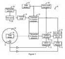
- Figure 1illustrates a communications receiver 10. It will be appreciated that Figure 1 is a functional representation of the communications receiver. Thus, while several of the functions of the receiver are shown as separate blocks in Figure 1 , in practice they might all be performed in a single suitable programmed processor.
- PCBprinted circuit board
- the communications receiver 10is suitable for operation as a portable communications device, such as a cellular handset, and therefore includes cellular transceiver circuitry 12, which is generally conventional, except as described below.
- the cellular transceiver circuitry 12operates on the basis of a clock signal, having a known nominal frequency, which is generated on the basis of a signal received from an oscillator 14.
- the oscillator 14does not need to be provided with any temperature compensation, thereby allowing the use of a low-cost crystal oscillator.
- the crystal oscillatorwill have a frequency-temperature characteristic in the form of a curve, which can be characterised by a number of parameters, as discussed in more detail below.
- the communications receiver 10further includes a Global Navigation Satellite System (GNSS) receiver circuit 16, as will be described in more detail below.
- GNSSGlobal Navigation Satellite System
- the temperature compensationis performed within the GNSS receiver using accurate knowledge of the frequency of the oscillator, as well as the rate of change of the frequency (i.e. the frequency drift rate).
- the rate of change of the frequency drift ratei.e. the frequency acceleration
- ffrequency
- ttime
- Ttemperature
- the frequency accelerationdepends on the crystal curve curvature multiplied with temperature drift squared and crystal curve slope multiplied with temperature acceleration. Due to the sine-wave like crystal profile the two terms add up orthogonally, i.e. when the curvature is large the slope is small and the other way around.
- the crystal profile curvatureis around 36ppb/K 2 at the turning points which leads together with a frequency drift of 0.15K/s to frequency acceleration of around 0.8ppb/s 2 .
- frequency accelerationis negligible, and accurate frequency tracking can be performed based on linearly extrapolating the estimated frequency drift in time.
- the second term in the above equationmay lead to higher frequency acceleration in the presence of thermal shocks (i.e. large temperature acceleration) typically caused by heat sources that located close to the crystal unit. To retain high sensitivity of the GNSS receiver, such thermal shocks need to be taken into account.
- FIG. 2is a block schematic diagram, showing in more detail the form of the GNSS receiver 16, and its connection to the oscillator 14.
- the receiver 16includes an antenna 160, analog RF receiver circuitry 162, and GNSS digital baseband circuitry 164.
- the RF circuitry 162includes a low-noise amplifier (LNA) 170, for amplifying signals received by the antenna 160.
- LNAlow-noise amplifier
- the amplified signalsare passed to a mixer 172, where they are downconverted to intermediate frequency (IF).
- the mixer 172downconverts the received signal based on a signal received from a synthesiser 174, which in turn receives the signal generated by the oscillator 14.
- the downconverted signalis passed from the mixer 172 to an analog-digital converter 176, and the digital IF signal is passed to the digital baseband block 164.
- the synthesiser 174generates a signal at a nominal frequency, which is also passed to a numerically controlled oscillator (NCO) 180 in the GNSS baseband block 164.
- the NCO 180generates a signal at the relevant intermediate frequency, for converting the IF signal to baseband in a mixer 182.
- the baseband signalis then passed to separate mixers 184a, 184b, 184c, which receive separate satellite identification codes from a respective code block 186a, 186b, 186c, in order to determine the respective correlations with the satellite identification codes, and form separate received signals from the available satellite vehicles (SVs) that are visible at the present time.
- SVssatellite vehicles
- the resulting signalsare passed to separate I&Q accumulator blocks 192a, 192b, 192c, where they are detected.
- the results of these signal detectionsare passed to a measurement engine (ME) processor 194.
- the ME processor 194is able to calculate the position to a high degree of accuracy, provided that it is able to obtain the required fix on the signals transmitted by the SVs.
- the ME processor 194is also connected by a serial communications link 196 to the other components of the receiver 10, as shown in Figure 1 , as described in more detail below.
- the receiver 10, shown in Figure 1also includes a temperature sensor 18, for example in the form of a thermistor.
- the temperature sensor 18is located close as possible to the oscillator 14, so that it can provide an accurate measurement of the temperature of the oscillator, at least to within the limits of the accuracy of the temperature sensor.
- the PCB-mounted temperature sensor 18might typically be in the form of a negative temperature coefficient (NTC) resistor in series with a fixed resistor. When a known current or voltage is applied, the voltage drop across the NTC device is measured using an analog-digital converter (ADC).
- ADCanalog-digital converter
- the resolution of the temperature sensor 18needs to be fine enough to accurately measure temperature once the product has learned the crystal profile. For example, a temperature .resolution of ⁇ 0.15K might be required. In any event, sensors of this type have limited accuracy, meaning that it is undesirable to use only such temperature measurements, particularly in view of the uncertainty of the crystal temperature-frequency profile, for frequency estimation.
- NTC sensorsare relatively low in cost
- an array of sensors mounted around the crystalmay be used to capture transient behaviour more accurately. For example, if two or more NTC resistors are placed around the crystal, the averaged temperature estimate will improve the measurements in a dynamic situation. In effect, the array of sensors form a temperature sensor producing a measure of the temperature of the oscillator from their combined individual measurements.
- the temperature of the oscillator 14can be kept as constant as possible in use, and so the oscillator 14 and the temperature sensor 18 are mounted together on the PCB in an area that is as far as possible thermally isolated from the other components of the receiver, in order to minimise the effects of other parts of the receiver on the temperature of the oscillator.
- the module containing the oscillator 14 and the temperature sensor 18can be connected to the PCB by means of a small number of relatively narrow copper bridges, providing good electrical conductivity but poor thermal conductivity.
- temperature measurements from the temperature sensor 18provide a means of estimating the current clock frequency.
- a mathematical model of the clock frequency against temperature characteristicis stored in flash memory 20 of the receiver.
- An initial factory modelmay be programmed into the device, with provision for learning a more exact relationship for the particular crystal fitted, during use.
- the modelshould have parameters to describe a third order temperature curve, an initial offset, and changes due to ageing, at least.
- crystal oscillatorsmay exhibit so-called micro-jumps. As the temperature moves through a certain value, the frequency steps by a certain amount. The points at which these jumps occur are different from sample to sample. However, for a given sample they occur at roughly the same temperature value each time. Predictive estimation of temperature changes therefore allows the GNSS receiver to anticipate a frequency step as well as correct for it once it has occurred.
- the measured temperature of the oscillatoris therefore used by a temperature-to-frequency conversion block 22 to form an estimate of the clock frequency, based on the characteristic stored in the memory 20.
- the cellular transceiver 12provides a means for forming an estimate of the current clock frequency when the cellular transceiver 12 is frequency locked to the cellular network. That is, the cellular transceiver must transmit signals to the cellular network at frequencies that have frequency errors of no more than 0.1 ppm, compared with the nominal frequencies, and similarly rely on the clock frequency being sufficiently close to the nominal frequency in order to be able to receive signals transmitted by the network successfully. Thus, the cellular transceiver 12 is able to estimate the frequency of the clock signal received from the oscillator 14.
- the first estimate of the current clock frequency produced by the temperature-to-frequency conversion block 22, and the second estimate of the current clock frequency produced by the cellular transceiver 12are then passed to a combiner 24, which forms a combined estimate of the current clock frequency, depending on the usage situation of the receiver 10.
- the absolute tolerance of the estimate from the communications transceiver 12is better than the tolerance of the temperature based estimate.
- the estimate from the communications transceiver 12is noisier, and is affected by user motion. In particular, this makes it less suitable for estimating the frequency rate of change. For this parameter, estimates based on temperature measurements are critical.
- the GNSS receiver 16is successfully tracking satellite signals, especially at high signal to noise ratios, it too is able to provide estimates for the frequency and rate of frequency change of the oscillator 14, and these estimates are typically more accurate than those that can be obtained from the communications transceiver or from the temperature measurements.
- the estimates provided by the GNSS receiverare also passed to the combiner 24, which produces a combined estimate of the frequency, based on these estimates.
- the receiverattempts to anticipate changes in the frequency. Specifically, changes in the usage of the receiver cause heat to be generated in the device, which in turn cause changes in the temperature of the oscillator, and hence changes in the frequency. As described below, the combined estimate can be corrected based on dynamic temperature changes.
- the receiverincludes a component 26 that acts as a heat source. That is, the component generates heat at certain times.
- the heat source 26might be the cellular transceiver chip 12, where this is provided as a single separate integrated circuit. In general, there may be multiple such heat sources, all of which can be taken into consideration in the same way.
- the heat source 26does not act as a constant source of heat, but rather it only generates heat at certain times, for example when the receiver 10 is in a cellular call, or is transmitting data over a cellular wireless link.
- the operation of the heat sourceis monitored by a controller 28, which has information about the components of the receiver 10 that are in use.
- the information about the usage of the various heat sourcesis passed to a thermal model 30, which is used to model and predict rapid changes in temperature of the oscillator crystal.
- Figure 3is a schematic representation of the thermal model 30, representing the heat flow between the heat source and the crystal module.
- Figure 3represents the various parameters in terms of an equivalent electrical circuit, in which electrical resistance represents thermal resistance (in Kelvin/Watt), electrical capacitance represents heat capacitance (in Joules/Kelvin), electric current represents heat flow (in Watts), and the equivalent of voltage is temperature (in Kelvin).
- Figure 3shows a typical form of a thermal model, in the case where only one heat source 26 is located close enough to the crystal unit 14 on the PCB to cause significant temperature acceleration.
- the crystal temperatureis ultimately affected by the ambient temperature, and by all heat sources in the user device, such as power amplifiers, display drivers, and the like.
- a dedicated thermal design of the receiverpreferably ensures that the crystal temperature evolves slowly i.e. thermal time constants of tens of seconds or longer.
- the crystal unit 14 and temperature sensor 18are co-located several millimetres away from the nearest heat source, and a thermal break 50 (resulting from gaps in copper layers in the PCB) encircles the two components 52.
- the thermally isolated areais kept large (several millimetres radius) to provide significant thermal capacitance..With these simple measures, only very few components located on the PCB have the potential to cause rapid changes in crystal temperature.
- the thermal model 30contains various thermal resistances 54 and capacitances 56, where the topology and the component values are chosen so as to capture the changes in the temperature of the oscillator 14 due to the heat source 26.
- the resistances 54 and capacitances 56 to the left of the dashed line 56represent the properties of the PCB outside the thermal break 50, while the resistances 54 and capacitances 56 to the right of the dashed line 56 represent the properties of the PCB inside the thermal break 50.
- the modelis chosen to capture the underlying mechanical properties.
- Thermal resistance on a PCBrelates primarily to the presence of copper connections, because the glass-fibre substrate material is a poor conductor of heat.
- Specific heat capacitanceis an intrinsic material property, and the total heat capacitance is dependent on the material dimensions.
- the purpose of the modelis to react quickly to changes in temperature that will be caused by changes in the heat input from the heat source 26, and so the model does not require accurate modelling of slow variations in temperature, which are directly tracked by the temperature sensor.
- the temperature dynamics of the crystal oscillatormay be found by integrating the heating power injected by the heat source 26 in time.
- the thermal model 30is resident on a processor, and the integration is performed numerically in the processor by filtering sampled values of the injected heating power.
- the filter coefficientsare chosen such that the filtering yields the same transfer function from heat source to crystal unit as the nodal model 30.
- Figures 1 and 3shows only a single temperature sensor, positioned such that it can detect the temperature of the crystal oscillator, further temperature sensors positioned on the circuit board can also provide useful information, for example in confirming the accuracy of the thermal model.
- the thermal model 30can be used to estimate the effect of the nearby heat sources 26 on the temperature of the oscillator 14, over the next one second. This is passed to the temperature-to-frequency conversion block 22, to determine an estimated effect of the nearby heat sources 26 on the frequency of the oscillator 14, over the next one second. This estimated effect is then added in the block 32 to the estimated current value of the frequency derived in the block 24.
- the resulting prediction of the frequencyis used to provide a frequency aiding update to the GNSS receiver 16.
- the frequency aiding updateis supplied to the ME processor 194 of the GNSS receiver 16 over the serial communications link 196 at a rate of typically once per second. Because the time delay between changing the injected heating current and a temperature change in the crystal is larger than the one second update rate, this model is able to forecast temperature and therefore frequency changes due to the local heat source.
- the GNSS receiver 16is provided with a frequency and rate of frequency change estimate once a second. As long as the frequency acceleration (d 2 f/dt 2 ) is small, these parameters allow the GNSS receiver to counteract movements in the reference clock by linearly extrapolating the frequency evolution over the following second. If, however, the frequency acceleration is larger, exceeding roughly 10Hz/s 2 , the performance may be degraded because the satellite signal moves outside the receiver bandwidth over the time between two frequency updates. Because fast frequency acceleration is caused by temperature acceleration, the extrapolation error may be removed by adjusting the frequency drift estimate before it is sent to the GNSS receiver. As a result, the GNSS signal stays within the receiver bandwidth for the duration between two frequency aiding updates, even when the crystal unit is subject to thermal shocks.
- Figure 4is a flow chart, illustrating a method in accordance with an aspect of the invention, performed in the combiner 24 and the adder 32, it being understood Figure 1 shows these components schematically, and that these functions might advantageously be performed in a processor within the GNSS receiver 16.
- the combiner 24receives the estimate of the current frequency of the oscillator 14, based on the measurement from the temperature sensor 18, and based on the stored temperature-frequency characteristic.
- the combiner 24receives the estimate of the current frequency of the oscillator 14, from the cellular transceiver 12, if such an estimate is available.
- the combiner 24receives the estimate of the current frequency of the oscillator 14, from the GNSS receiver 16, if such an estimate is available.
- step 76these estimates are weighted, to form a combined estimate.
- the resulting informationmight consist of: an estimate of current frequency, an estimate of the rate of change of frequency, an error margin for the frequency estimate, and an error margin of the frequency rate estimate, where the error margins relate to the maturity of the crystal curve (i.e. the frequency versus measured temperature characteristic of the crystal) model.
- the weighting of the different estimatesvaries over time.
- the estimates based on the measured temperature and derived from the cellular transceivermight have different reliabilities at different times, and the estimate derived from the GNSS receiver 16 itself might be the most reliable when the receiver is locked onto the satellite signals.
- step 78the predicted effect of the heat sources 26 on the frequency, resulting from the predicted effect on the temperature of the oscillator 14, is added to the combined estimate of the current frequency, in order to form an estimate of the frequency that will be usable for the next second.
- each SV channelhas its own Doppler NCO 190a, 190b, 190c, while the whole baseband has a common IF NCO 180, which is programmed to remove the final IF frequency.
- This same IF NCO 180is also useful for removing any reference frequency offsets. Therefore, in the illustrated embodiment, the clock frequency drift corrections are applied in the IF NCO 180. Once the drift and steps are removed by the IF NCO, the following circuits only experience the Doppler as they would have done with an uncorrupted clock.
- the frequency aiding updatecan be applied either to tune the crystal oscillator directly, to change the synthesizer 174 that feeds the mixer 172 that downconverts the received signal from RF to IF, or in the individual Doppler NCOs 190a, 190b, 190c for each satellite.
- the combined estimate of the current frequencyis fed back to a block 54, where it is used to determine whether it is necessary to refine the currently stored crystal curve. If so, any change is stored in the flash memory 20 of the receiver 10.
- the frequency modele.g. a 5 th order polynomial
- a model of its uncertainty or errore.g. a polynomial with only even order terms so that the error is strictly positive.
- the frequency modelcan be updated and the associated uncertainty reduced.
- This schemecan run continuously, using only the estimates from the cellular transceiver and based on the measured temperature, even before the GNSS receiver 16 is enabled for the first time. This means that a good estimate of frequency, perhaps based only on temperature measurements, can be available before the GNSS receiver requires it.
- the present inventionprovides a system whereby, based on the system activity, crystal temperature movements are forecast, allowing the GNSS receiver to anticipate frequency movements accordingly.
Landscapes
- Engineering & Computer Science (AREA)
- Radar, Positioning & Navigation (AREA)
- Remote Sensing (AREA)
- Computer Networks & Wireless Communication (AREA)
- Physics & Mathematics (AREA)
- General Physics & Mathematics (AREA)
- Superheterodyne Receivers (AREA)
Description
- This invention relates to a telecommunications device, and in particular to a method for compensating for changes in the temperature of the device, and to a device operating in accordance with the method.
- Typically, telecommunications devices include an oscillator, which is used to generate signals at a known frequency, in order to be able to transmit and receive signals successfully at the required frequencies. It is known that such oscillators have temperature dependent frequency characteristics. Where the signals need to be generated such that their frequency is known with a very high degree of accuracy and stability, for example in Global Navigation Satellite System (GNSS) receivers, it is common to try to minimize, and then to compensate for, changes in the temperature of the oscillator.
US-6,630,872 relates to a communications receiver, in which signal reception relies on a signal generated by an oscillator circuit in the receiver. It is known that such oscillator circuits are sensitive to changes in ambient temperature, and the document discloses a system in which a temperature sensor is coupled to the oscillator. A thermal model of the oscillator and its environment is used, so that a temperature value generated by the temperature sensor can be used to estimate a true temperature of the oscillator. Knowledge of the temperature-frequency characteristic of the oscillator can then be used to estimate the true frequency of the signal generated by the oscillator circuit.WO 2008/021810 A2 discloses a communication device which estimates the frequency generated by a temperature-dependent oscillator based on measurements from a temperature sensor having a known positional relationship to the oscillator, and based on the temperature-dependent frequency characteristic of the oscillator.- According to a first aspect of the present invention, there is provided a communications device, comprising: an oscillator, having a temperature-dependent frequency characteristic, for generating signals at a nominal frequency; receiver circuitry, for receiving transmitted wireless signals using the signals generated by the oscillator; at least one temperature sensor, having a known positional relationship to the oscillator; an estimation device, for estimating a frequency of the signals generated by the oscillator, based on a measurement from the temperature sensor, and based on the temperature-dependent frequency characteristic of the oscillator; at least one heat source;
wherein the temperature sensor and the oscillator are mounted on a printed circuit board and co-located away from the heat source in a thermally isolated area surrounded by a thermal break, wherein the thermal break comprises gaps in copper layers in the PCB; a prediction device, for predicting a change in temperature of the oscillator, based on a state of the heat source, and further based on a model of the thermal properties of the communications device, and hence for predicting a rate of change in the frequency of the signals generated by the oscillator, based on the temperature-dependent frequency characteristic of the oscillator, wherein the receiver circuitry uses the estimated frequency of the signals generated by the oscillator, and the predicted rate of change in the frequency of the signals generated by the oscillator, in receiving the transmitted wireless signals. - According to a second aspect of the present invention, there is provided a method of operation of a communications device, the communications device comprising: an oscillator, having a temperature-dependent frequency characteristic, for generating signals at a nominal frequency; receiver circuitry, for receiving transmitted wireless signals using the signals generated by the oscillator; at least one temperature sensor, having a known positional relationship to the oscillator; and at least one heat source;
wherein the temperature sensor and the oscillator are mounted on a printed circuit board and co-located away from the heat source in a thermally isolated area surrounded by a thermal break, wherein the thermal break comprises gaps in copper layers in the PCB; the method comprising: estimating a frequency of the signals generated by the oscillator, based on a measurement from the temperature sensor, and based on the temperature-dependent frequency characteristic of the oscillator; predicting a change in temperature of the oscillator, based on a state of the heat source, and further based on a model of the thermal properties of the communications device, and hence predicting a rate of change in the frequency of the signals generated by the oscillator, based on the temperature-dependent frequency characteristic of the oscillator, and using the estimated frequency of the signals generated by the oscillator, and the predicted rate of change in the frequency of the signals generated by the oscillator, in receiving the transmitted wireless signals in the receiver circuitry. - This has the advantage that the device can react more quickly to rapid changes in oscillator temperature caused by system activity, and thereby reduce transient frequency errors that occur with conventional temperature controlled crystal oscillators (TCXOs).
Figure 1 is a block schematic diagram of a communications receiver in accordance with an aspect of the invention.Figure 2 is a schematic block diagram, illustrating in more detail a part of the receiver ofFigure 1 .Figure 3 illustrates the use of a thermal model, in the receiver ofFigure 1 .Figure 4 is a flow chart, illustrating a method in accordance with an aspect of the invention.Figure 1 illustrates acommunications receiver 10. It will be appreciated thatFigure 1 is a functional representation of the communications receiver. Thus, while several of the functions of the receiver are shown as separate blocks inFigure 1 , in practice they might all be performed in a single suitable programmed processor.- As is conventional, various components of the
receiver 10 are provided in separate integrated circuit devices, mounted on a printed circuit board (PCB). - In this illustrated embodiment, the
communications receiver 10 is suitable for operation as a portable communications device, such as a cellular handset, and therefore includescellular transceiver circuitry 12, which is generally conventional, except as described below. - As is conventional, the
cellular transceiver circuitry 12 operates on the basis of a clock signal, having a known nominal frequency, which is generated on the basis of a signal received from anoscillator 14. In this illustrated embodiment, theoscillator 14 does not need to be provided with any temperature compensation, thereby allowing the use of a low-cost crystal oscillator. The crystal oscillator will have a frequency-temperature characteristic in the form of a curve, which can be characterised by a number of parameters, as discussed in more detail below. - In this illustrated embodiment, the
communications receiver 10 further includes a Global Navigation Satellite System (GNSS)receiver circuit 16, as will be described in more detail below. In the architecture shown inFigure 1 , the temperature compensation is performed within the GNSS receiver using accurate knowledge of the frequency of the oscillator, as well as the rate of change of the frequency (i.e. the frequency drift rate). The rate of change of the frequency drift rate (i.e. the frequency acceleration) is not directly estimated from frequency measurements.. - The rate of change of frequency drift rate can be written as


- Thus, the frequency acceleration depends on the crystal curve curvature multiplied with temperature drift squared and crystal curve slope multiplied with temperature acceleration. Due to the sine-wave like crystal profile the two terms add up orthogonally, i.e. when the curvature is large the slope is small and the other way around. Using figures for a typical communications device, the crystal profile curvature is around 36ppb/K2 at the turning points which leads together with a frequency drift of 0.15K/s to frequency acceleration of around 0.8ppb/s2. At this level, frequency acceleration is negligible, and accurate frequency tracking can be performed based on linearly extrapolating the estimated frequency drift in time. The second term in the above equation may lead to higher frequency acceleration in the presence of thermal shocks (i.e. large temperature acceleration) typically caused by heat sources that located close to the crystal unit. To retain high sensitivity of the GNSS receiver, such thermal shocks need to be taken into account.
Figure 2 is a block schematic diagram, showing in more detail the form of theGNSS receiver 16, and its connection to theoscillator 14.- Specifically, the
receiver 16 includes anantenna 160, analogRF receiver circuitry 162, and GNSSdigital baseband circuitry 164. TheRF circuitry 162 includes a low-noise amplifier (LNA) 170, for amplifying signals received by theantenna 160. The amplified signals are passed to amixer 172, where they are downconverted to intermediate frequency (IF). Themixer 172 downconverts the received signal based on a signal received from asynthesiser 174, which in turn receives the signal generated by theoscillator 14. The downconverted signal is passed from themixer 172 to an analog-digital converter 176, and the digital IF signal is passed to thedigital baseband block 164. - The
synthesiser 174 generates a signal at a nominal frequency, which is also passed to a numerically controlled oscillator (NCO) 180 in theGNSS baseband block 164. The NCO 180 generates a signal at the relevant intermediate frequency, for converting the IF signal to baseband in amixer 182. The baseband signal is then passed toseparate mixers respective code block Figure 2 , it will be appreciated that the number of such paths can be chosen to be any required number. - These separate signals are then passed to separate
further mixers NCO block receiver 10. - The resulting signals are passed to separate
I&Q accumulator blocks processor 194. As is known, theME processor 194 is able to calculate the position to a high degree of accuracy, provided that it is able to obtain the required fix on the signals transmitted by the SVs. - The
ME processor 194 is also connected by aserial communications link 196 to the other components of thereceiver 10, as shown inFigure 1 , as described in more detail below. - The
receiver 10, shown inFigure 1 , also includes atemperature sensor 18, for example in the form of a thermistor. Preferably, thetemperature sensor 18 is located close as possible to theoscillator 14, so that it can provide an accurate measurement of the temperature of the oscillator, at least to within the limits of the accuracy of the temperature sensor. The PCB-mountedtemperature sensor 18 might typically be in the form of a negative temperature coefficient (NTC) resistor in series with a fixed resistor. When a known current or voltage is applied, the voltage drop across the NTC device is measured using an analog-digital converter (ADC). The resolution of thetemperature sensor 18 needs to be fine enough to accurately measure temperature once the product has learned the crystal profile. For example, a temperature .resolution of <0.15K might be required. In any event, sensors of this type have limited accuracy, meaning that it is undesirable to use only such temperature measurements, particularly in view of the uncertainty of the crystal temperature-frequency profile, for frequency estimation. - Although reference is made here to a single temperature sensor, since NTC sensors are relatively low in cost, an array of sensors mounted around the crystal may be used to capture transient behaviour more accurately. For example, if two or more NTC resistors are placed around the crystal, the averaged temperature estimate will improve the measurements in a dynamic situation. In effect, the array of sensors form a temperature sensor producing a measure of the temperature of the oscillator from their combined individual measurements.
- It is advantageous if the temperature of the
oscillator 14 can be kept as constant as possible in use, and so theoscillator 14 and thetemperature sensor 18 are mounted together on the PCB in an area that is as far as possible thermally isolated from the other components of the receiver, in order to minimise the effects of other parts of the receiver on the temperature of the oscillator. For example, the module containing theoscillator 14 and thetemperature sensor 18 can be connected to the PCB by means of a small number of relatively narrow copper bridges, providing good electrical conductivity but poor thermal conductivity. - Thus, temperature measurements from the
temperature sensor 18 provide a means of estimating the current clock frequency. A mathematical model of the clock frequency against temperature characteristic is stored inflash memory 20 of the receiver. An initial factory model may be programmed into the device, with provision for learning a more exact relationship for the particular crystal fitted, during use. For example, the model should have parameters to describe a third order temperature curve, an initial offset, and changes due to ageing, at least. Furthermore, crystal oscillators may exhibit so-called micro-jumps. As the temperature moves through a certain value, the frequency steps by a certain amount. The points at which these jumps occur are different from sample to sample. However, for a given sample they occur at roughly the same temperature value each time. Predictive estimation of temperature changes therefore allows the GNSS receiver to anticipate a frequency step as well as correct for it once it has occurred. - The measured temperature of the oscillator is therefore used by a temperature-to-
frequency conversion block 22 to form an estimate of the clock frequency, based on the characteristic stored in thememory 20. - In addition, the
cellular transceiver 12 provides a means for forming an estimate of the current clock frequency when thecellular transceiver 12 is frequency locked to the cellular network. That is, the cellular transceiver must transmit signals to the cellular network at frequencies that have frequency errors of no more than 0.1 ppm, compared with the nominal frequencies, and similarly rely on the clock frequency being sufficiently close to the nominal frequency in order to be able to receive signals transmitted by the network successfully. Thus, thecellular transceiver 12 is able to estimate the frequency of the clock signal received from theoscillator 14. - The first estimate of the current clock frequency produced by the temperature-to-
frequency conversion block 22, and the second estimate of the current clock frequency produced by thecellular transceiver 12 are then passed to acombiner 24, which forms a combined estimate of the current clock frequency, depending on the usage situation of thereceiver 10. - In practice, the absolute tolerance of the estimate from the
communications transceiver 12 is better than the tolerance of the temperature based estimate. On the other hand, the estimate from thecommunications transceiver 12 is noisier, and is affected by user motion. In particular, this makes it less suitable for estimating the frequency rate of change. For this parameter, estimates based on temperature measurements are critical. - Once the
GNSS receiver 16 is successfully tracking satellite signals, especially at high signal to noise ratios, it too is able to provide estimates for the frequency and rate of frequency change of theoscillator 14, and these estimates are typically more accurate than those that can be obtained from the communications transceiver or from the temperature measurements. Thus, the estimates provided by the GNSS receiver are also passed to thecombiner 24, which produces a combined estimate of the frequency, based on these estimates. - As well as estimating the current frequency of the signals generated by the oscillator, the receiver attempts to anticipate changes in the frequency. Specifically, changes in the usage of the receiver cause heat to be generated in the device, which in turn cause changes in the temperature of the oscillator, and hence changes in the frequency. As described below, the combined estimate can be corrected based on dynamic temperature changes.
- Thus, as shown in
Figure 1 , the receiver includes acomponent 26 that acts as a heat source. That is, the component generates heat at certain times. For example, theheat source 26 might be thecellular transceiver chip 12, where this is provided as a single separate integrated circuit. In general, there may be multiple such heat sources, all of which can be taken into consideration in the same way. Thus, theheat source 26 does not act as a constant source of heat, but rather it only generates heat at certain times, for example when thereceiver 10 is in a cellular call, or is transmitting data over a cellular wireless link. - The operation of the heat source is monitored by a
controller 28, which has information about the components of thereceiver 10 that are in use. - The information about the usage of the various heat sources is passed to a
thermal model 30, which is used to model and predict rapid changes in temperature of the oscillator crystal. Figure 3 is a schematic representation of thethermal model 30, representing the heat flow between the heat source and the crystal module.Figure 3 represents the various parameters in terms of an equivalent electrical circuit, in which electrical resistance represents thermal resistance (in Kelvin/Watt), electrical capacitance represents heat capacitance (in Joules/Kelvin), electric current represents heat flow (in Watts), and the equivalent of voltage is temperature (in Kelvin).Figure 3 shows a typical form of a thermal model, in the case where only oneheat source 26 is located close enough to thecrystal unit 14 on the PCB to cause significant temperature acceleration. In principle, the crystal temperature is ultimately affected by the ambient temperature, and by all heat sources in the user device, such as power amplifiers, display drivers, and the like. However, a dedicated thermal design of the receiver preferably ensures that the crystal temperature evolves slowly i.e. thermal time constants of tens of seconds or longer. Thus, thecrystal unit 14 andtemperature sensor 18 are co-located several millimetres away from the nearest heat source, and a thermal break 50 (resulting from gaps in copper layers in the PCB) encircles the twocomponents 52. The thermally isolated area is kept large (several millimetres radius) to provide significant thermal capacitance..With these simple measures, only very few components located on the PCB have the potential to cause rapid changes in crystal temperature.- Thus, the
thermal model 30 contains variousthermal resistances 54 andcapacitances 56, where the topology and the component values are chosen so as to capture the changes in the temperature of theoscillator 14 due to theheat source 26. Theresistances 54 andcapacitances 56 to the left of the dashedline 56 represent the properties of the PCB outside thethermal break 50, while theresistances 54 andcapacitances 56 to the right of the dashedline 56 represent the properties of the PCB inside thethermal break 50. The model is chosen to capture the underlying mechanical properties. Thermal resistance on a PCB relates primarily to the presence of copper connections, because the glass-fibre substrate material is a poor conductor of heat. Specific heat capacitance is an intrinsic material property, and the total heat capacitance is dependent on the material dimensions. In this case, the purpose of the model is to react quickly to changes in temperature that will be caused by changes in the heat input from theheat source 26, and so the model does not require accurate modelling of slow variations in temperature, which are directly tracked by the temperature sensor. - Using the
thermal model 30, the temperature dynamics of the crystal oscillator may be found by integrating the heating power injected by theheat source 26 in time. Thethermal model 30 is resident on a processor, and the integration is performed numerically in the processor by filtering sampled values of the injected heating power. The filter coefficients are chosen such that the filtering yields the same transfer function from heat source to crystal unit as thenodal model 30. - Although
Figures 1 and3 shows only a single temperature sensor, positioned such that it can detect the temperature of the crystal oscillator, further temperature sensors positioned on the circuit board can also provide useful information, for example in confirming the accuracy of the thermal model. - Thus, the
thermal model 30 can be used to estimate the effect of thenearby heat sources 26 on the temperature of theoscillator 14, over the next one second. This is passed to the temperature-to-frequency conversion block 22, to determine an estimated effect of thenearby heat sources 26 on the frequency of theoscillator 14, over the next one second. This estimated effect is then added in theblock 32 to the estimated current value of the frequency derived in theblock 24. - The resulting prediction of the frequency is used to provide a frequency aiding update to the
GNSS receiver 16. Specifically, the frequency aiding update is supplied to theME processor 194 of theGNSS receiver 16 over the serial communications link 196 at a rate of typically once per second. Because the time delay between changing the injected heating current and a temperature change in the crystal is larger than the one second update rate, this model is able to forecast temperature and therefore frequency changes due to the local heat source. - As mentioned above, in this illustrated embodiment, the
GNSS receiver 16 is provided with a frequency and rate of frequency change estimate once a second. As long as the frequency acceleration (d2f/dt2) is small, these parameters allow the GNSS receiver to counteract movements in the reference clock by linearly extrapolating the frequency evolution over the following second. If, however, the frequency acceleration is larger, exceeding roughly 10Hz/s2, the performance may be degraded because the satellite signal moves outside the receiver bandwidth over the time between two frequency updates. Because fast frequency acceleration is caused by temperature acceleration, the extrapolation error may be removed by adjusting the frequency drift estimate before it is sent to the GNSS receiver. As a result, the GNSS signal stays within the receiver bandwidth for the duration between two frequency aiding updates, even when the crystal unit is subject to thermal shocks. Figure 4 is a flow chart, illustrating a method in accordance with an aspect of the invention, performed in thecombiner 24 and theadder 32, it being understoodFigure 1 shows these components schematically, and that these functions might advantageously be performed in a processor within theGNSS receiver 16.- Thus, in
step 70, thecombiner 24 receives the estimate of the current frequency of theoscillator 14, based on the measurement from thetemperature sensor 18, and based on the stored temperature-frequency characteristic. Instep 72, thecombiner 24 receives the estimate of the current frequency of theoscillator 14, from thecellular transceiver 12, if such an estimate is available. Instep 74, thecombiner 24 receives the estimate of the current frequency of theoscillator 14, from theGNSS receiver 16, if such an estimate is available. - In
step 76, these estimates are weighted, to form a combined estimate. The resulting information might consist of: an estimate of current frequency, an estimate of the rate of change of frequency, an error margin for the frequency estimate, and an error margin of the frequency rate estimate, where the error margins relate to the maturity of the crystal curve (i.e. the frequency versus measured temperature characteristic of the crystal) model. The weighting of the different estimates varies over time. As mentioned above, the estimates based on the measured temperature and derived from the cellular transceiver might have different reliabilities at different times, and the estimate derived from theGNSS receiver 16 itself might be the most reliable when the receiver is locked onto the satellite signals. - For example, if three estimates of drift are Dt, Dm, Dg, derived from the temperature,
cellular transceiver 12 andGNSS receiver 16 respectively, with respective accuracies At, Am, Ag, then a final, weighted, estimate of drift might be:
- In
step 78, the predicted effect of theheat sources 26 on the frequency, resulting from the predicted effect on the temperature of theoscillator 14, is added to the combined estimate of the current frequency, in order to form an estimate of the frequency that will be usable for the next second. - This estimate is then provided in
step 80 as a frequency aiding update for use in theGNSS receiver 16. In the illustrated embodiment shown inFigure 2 , each SV channel has itsown Doppler NCO common IF NCO 180, which is programmed to remove the final IF frequency. This same IFNCO 180 is also useful for removing any reference frequency offsets. Therefore, in the illustrated embodiment, the clock frequency drift corrections are applied in theIF NCO 180. Once the drift and steps are removed by the IF NCO, the following circuits only experience the Doppler as they would have done with an uncorrupted clock. - As alternatives, the frequency aiding update can be applied either to tune the crystal oscillator directly, to change the
synthesizer 174 that feeds themixer 172 that downconverts the received signal from RF to IF, or in theindividual Doppler NCOs - Also, in
step 82, the combined estimate of the current frequency is fed back to ablock 54, where it is used to determine whether it is necessary to refine the currently stored crystal curve. If so, any change is stored in theflash memory 20 of thereceiver 10. The frequency model (e.g. a 5th order polynomial) is stored in conjunction with a model of its uncertainty or error (e.g. a polynomial with only even order terms so that the error is strictly positive). Whenever a frequency measurement with good accuracy is available, then the frequency model can be updated and the associated uncertainty reduced. This scheme can run continuously, using only the estimates from the cellular transceiver and based on the measured temperature, even before theGNSS receiver 16 is enabled for the first time. This means that a good estimate of frequency, perhaps based only on temperature measurements, can be available before the GNSS receiver requires it. - Thus, the present invention provides a system whereby, based on the system activity, crystal temperature movements are forecast, allowing the GNSS receiver to anticipate frequency movements accordingly.


Claims (15)
- A communications device, comprising:an oscillator (14), having a temperature-dependent frequency characteristic, for generating signals at a nominal frequency;receiver circuitry (16), for receiving transmitted wireless signals using the signals generated by the oscillator;at least one temperature sensor (18), having a known positional relationship to the oscillator (14);an estimation device (24), for estimating a frequency of the signals generated by the oscillator (14), based on a measurement from the temperature sensor (18), and based on the temperature-dependent frequency characteristic of the oscillator (14);at least one heat source (26);wherein the temperature sensor (18) and the oscillator (14) are mounted on a printed circuit board (PCB) and co-located away from the heat source (26) in a thermally isolated area surrounded by a thermal break (50), wherein the thermal break (50) comprises gaps in copper layers in the PCB; and;a prediction device (32), for predicting a change in temperature of the oscillator (14), based on a state of the heat source (26), and further based on a model of the thermal properties of the communications device, and hence for predicting a rate of change in the frequency of the signals generated by the oscillator (14), based on the temperature-dependent frequency characteristic of the oscillator (14),wherein the receiver circuitry (16) uses the estimated frequency of the signals generated by the oscillator (14), and the predicted rate of change in the frequency of the signals generated by the oscillator (14), in receiving the transmitted wireless signals.
- The communications device as claimed in claim 1, wherein the heat source (26) is a component of the communications device, and the prediction device (32) is adapted to predict an increase in temperature of the oscillator (14) following activation of the component.
- The communications device as claimed in claim 2, wherein the heat source (26) is a transceiver circuit of the communications device.
- The communications device as claimed in any preceding claim, wherein the prediction device (32) is further adapted to update the model of the temperature-dependent frequency characteristic of the oscillator (14) based on successfully received signals.
- The communications device as claimed in any preceding claim, wherein the receiver circuitry (16) is adapted to receive frequency aiding updates at predetermined time intervals, and the prediction device (32) is adapted to predict, for each of said predetermined time intervals, a change in the frequency of the signals generated by the oscillator (14) over said time interval.
- The communications device as claimed in any preceding claim, wherein the receiver circuitry (16) comprises a GNSS receiver, comprising a downconversion mixer, for downconverting a frequency of a received signal based on an oscillator signal, and individual oscillators for tracking signals from respective satellite vehicles, and wherein the receiver circuitry uses the estimated frequency of the signals generated by the oscillator, and the predicted change in the frequency of the signals generated by the oscillator, in the downconversion mixer.
- The communications device as claimed in claim 6, wherein the estimation device (24) estimates the frequency of the signals generated by the oscillator (14), based also on measurements from the GNSS receiver (16).
- The communications device as claimed in claim 6 or 7, further comprising cellular transceiver circuitry (12), for communicating in a cellular communications network, wherein the estimation device (24) estimates the frequency of the signals generated by the oscillator (14), based also on measurements from the cellular transceiver (12).
- A method of operation of a communications device, the communications device comprising:an oscillator (14), having a temperature-dependent frequency characteristic, for generating signals at a nominal frequency;receiver circuitry (16), for receiving transmitted wireless signals using the signals generated by the oscillator; (14)at least one temperature sensor (18), having a known positional relationship to the oscillator (14); andat least one heat source (26);wherein the temperature sensor (18) and the oscillator (14) are mounted on a printed circuit board (PCB) and co-located away from the heat source (26) in a thermally isolated area surrounded by a thermal break (50), wherein the thermal break (50) comprises gaps in copper layers in the PCB; the method comprising:estimating a frequency of the signals generated by the oscillator (14), based on a measurement from the temperature sensor (18), and based on the temperature-dependent frequency characteristic of the oscillator (14);predicting a change in temperature of the oscillator (14), based on a state of the heat source (26), and further based on a model of the thermal properties of the communications device, and hence predicting a rate of change in the frequency of the signals generated by the oscillator (14), based on the temperature-dependent frequency characteristic of the oscillator (14), andusing the estimated frequency of the signals generated by the oscillator (14), and the predicted rate of change in the frequency of the signals generated by the oscillator (14), in receiving the transmitted wireless signals in the receiver circuitry (16).
- The method as claimed in claim 9, wherein the heat source (26) is a component of the communications device, comprising predicting an increase in temperature of the oscillator (14) following activation of the component.
- The method as claimed in claim 10, comprising updating the model of the temperature-dependent frequency characteristic of the oscillator (14) based on successfully received signals.
- The method as claimed in one of claims 9 to 11, comprising predicting, for each of a plurality of predetermined time intervals, a change in the frequency of the signals generated by the oscillator (14) over said time interval, and using the predicted changes in the receiver circuitry (16) during the predetermined time intervals.
- The method as claimed in any of claims 9 to 12, wherein the receiver circuitry (16) comprises a GNSS receiver, and wherein the GNSS receiver circuitry comprises a downconversion mixer, for downconverting a frequency of a received signal based on an oscillator signal, and individual oscillators for tracking signals from respective satellite vehicles, and wherein the method comprises using the estimated frequency of the signals generated by the oscillator, and the predicted change in the frequency of the signals generated by the oscillator, in the downconversion mixer.
- The method as claimed in claim 13, comprising estimating the frequency of the signals generated by the oscillator (14), based also on measurements from the GNSS receiver.
- The method as claimed in any of claims 13 to 14, wherein the communications device further comprises cellular transceiver circuitry (12), for communicating in a cellular communications network, and the method comprises estimating the frequency of the signals generated by the oscillator (14), based also on measurements from the cellular transceiver (12).
Applications Claiming Priority (2)
| Application Number | Priority Date | Filing Date | Title |
|---|---|---|---|
| US17380009P | 2009-04-29 | 2009-04-29 | |
| PCT/GB2010/050693WO2010125388A1 (en) | 2009-04-29 | 2010-04-28 | Temperature compensation in a telecommunications device |
Publications (2)
| Publication Number | Publication Date |
|---|---|
| EP2425532A1 EP2425532A1 (en) | 2012-03-07 |
| EP2425532B1true EP2425532B1 (en) | 2015-05-20 |
Family
ID=42236678
Family Applications (1)
| Application Number | Title | Priority Date | Filing Date |
|---|---|---|---|
| EP20100720024Not-in-forceEP2425532B1 (en) | 2009-04-29 | 2010-04-28 | Temperature compensation in a telecommunications device |
Country Status (3)
| Country | Link |
|---|---|
| US (1) | US8693969B2 (en) |
| EP (1) | EP2425532B1 (en) |
| WO (1) | WO2010125388A1 (en) |
Families Citing this family (14)
| Publication number | Priority date | Publication date | Assignee | Title |
|---|---|---|---|---|
| US8775851B2 (en) | 2010-12-13 | 2014-07-08 | Maxlinear, Inc. | Method and system for precise temperature and timebase PPM error estimation using multiple timebases |
| EP2555431B1 (en)* | 2011-08-03 | 2018-02-28 | BlackBerry Limited | Electronic device including predicted frequency error estimation of a voltage controlled oscillator and related methods |
| US8710938B2 (en) | 2011-08-03 | 2014-04-29 | Blackberry Limited | Electronic device including predicted frequency error estimation of a voltage controlled oscillator and related methods |
| US9151845B2 (en)* | 2012-01-05 | 2015-10-06 | Cambridge Silicon Radio Limited | Reverse frequency and time aiding |
| US8912956B2 (en) | 2012-03-09 | 2014-12-16 | Csr Technology Inc. | Cooperative calibration of platform shared voltage controlled oscillator |
| US20140004887A1 (en)* | 2012-06-29 | 2014-01-02 | Qualcomm Incorporated | Crystal oscillator calibration |
| US9185659B2 (en) | 2012-10-25 | 2015-11-10 | Qualcomm Incorporated | Two-dimensional transmit power compensation |
| US10149261B2 (en)* | 2013-11-04 | 2018-12-04 | Qualcomm Incorporated | Methods and systems for mobile device clock management |
| US9476989B2 (en)* | 2014-04-16 | 2016-10-25 | Honeywell International Inc. | Vector tracking loop operability through oscillator micro-jump event |
| US10557944B2 (en) | 2014-10-27 | 2020-02-11 | Qualcomm Incorporated | Timing circuit calibration |
| US10509434B1 (en)* | 2016-09-27 | 2019-12-17 | Amazon Technologies, Inc. | Oscillator profiling for time synchronization |
| KR102685409B1 (en) | 2019-09-02 | 2024-07-15 | 삼성전자주식회사 | Electronic device |
| GB2596277B (en)* | 2020-05-28 | 2022-06-15 | Nordic Semiconductor Asa | Radio device with resonator |
| CN112187379A (en)* | 2020-09-17 | 2021-01-05 | 国家无线电监测中心 | High-reliability high-precision radio monitoring receiving system suitable for ultralow temperature environment |
Family Cites Families (30)
| Publication number | Priority date | Publication date | Assignee | Title |
|---|---|---|---|---|
| US4939786A (en)* | 1987-03-09 | 1990-07-03 | Motorola, Inc. | Adaptive thermal protection for a power amplifier by remote sense |
| US5654718A (en) | 1994-10-06 | 1997-08-05 | Garmin Corporation | GPS receiver device and method for calibrating a temperature uncompensated crystal oscillator |
| US5594453A (en)* | 1994-11-01 | 1997-01-14 | Trimble Navigation, Ltd | GPS receiver having a rapid acquisition of GPS satellite signals |
| US6002363A (en) | 1996-03-08 | 1999-12-14 | Snaptrack, Inc. | Combined GPS positioning system and communications system utilizing shared circuitry |
| US6122506A (en)* | 1998-05-04 | 2000-09-19 | Trimble Navigation Limited | GSM cellular telephone and GPS receiver combination |
| US6463266B1 (en)* | 1999-08-10 | 2002-10-08 | Broadcom Corporation | Radio frequency control for communications systems |
| US6928275B1 (en) | 2000-05-08 | 2005-08-09 | Qualcomm Incorporated | Method and apparatus for compensating local oscillator frequency error |
| US7929928B2 (en)* | 2000-05-18 | 2011-04-19 | Sirf Technology Inc. | Frequency phase correction system |
| US6933788B2 (en)* | 2001-05-16 | 2005-08-23 | Kyocera Wireless Corp. | Reference oscillator |
| US6630872B1 (en) | 2001-07-20 | 2003-10-07 | Cmc Electronics, Inc. | Digital indirectly compensated crystal oscillator |
| US6965754B2 (en) | 2001-10-09 | 2005-11-15 | Motorola, Inc. | Satellite positioning system receiver with reference oscillator circuit and methods therefor |
| US7010307B2 (en)* | 2002-02-22 | 2006-03-07 | Global Locate, Inc. | Method and apparatus for compensating an oscillator in a location-enabled wireless device |
| US6937872B2 (en) | 2002-04-15 | 2005-08-30 | Qualcomm Incorporated | Methods and apparatuses for measuring frequencies of basestations in cellular networks using mobile GPS receivers |
| JP2006506832A (en) | 2002-05-17 | 2006-02-23 | モトローラ・インコーポレイテッド | Frequency management in communication positioning equipment |
| GB0223351D0 (en) | 2002-10-08 | 2002-11-13 | Parthus Ireland Ltd | Mobile position fixing |
| US7359711B2 (en) | 2002-10-31 | 2008-04-15 | Siemens Communications, Inc. | Methods and apparatus for improving accuracy of radio timing measurements |
| US7362263B2 (en) | 2003-09-04 | 2008-04-22 | Seiko Epson Corporation | Keeping accurate time for a hybrid GPS receiver and mobile phone when powered off |
| US7012563B1 (en) | 2004-09-10 | 2006-03-14 | Motorola, Inc. | Method and system for frequency drift prediction |
| US7459984B2 (en) | 2005-05-26 | 2008-12-02 | Sirf Technology Holdings, Inc. | Method and apparatus for self-calibration and adaptive temperature compensation in GPS receivers |
| US7865158B2 (en)* | 2005-07-26 | 2011-01-04 | Interdigital Technology Corporation | Method and apparatus for automatically correcting receiver oscillator frequency |
| US8014476B2 (en) | 2005-11-07 | 2011-09-06 | Qualcomm, Incorporated | Wireless device with a non-compensated crystal oscillator |
| US7720469B2 (en)* | 2005-12-29 | 2010-05-18 | Nokia Corporation | Frequency calibration of wireless telecommunication device |
| US7456782B2 (en) | 2005-12-29 | 2008-11-25 | Sirf Technology, Inc. | Timing calibration for fast signal reacquisition in navigational receivers |
| CA2656113A1 (en)* | 2006-07-21 | 2008-01-24 | Ecole De Technologie Superieure | Voltage-controlled oscillator (vco) |
| US7742785B2 (en) | 2006-08-09 | 2010-06-22 | Qualcomm Incorporated | Reference signal generation for multiple communication systems |
| US7466209B2 (en) | 2007-01-05 | 2008-12-16 | Sirf Technology, Inc. | System and method for providing temperature correction in a crystal oscillator |
| US7477189B2 (en) | 2007-01-30 | 2009-01-13 | Sirf Technology Holdings, Inc. | Methods and systems for acquisition, reacquisiton and tracking of weak navigational signals |
| US7586382B2 (en) | 2007-01-30 | 2009-09-08 | Sirf Technology, Inc. | Methods and systems for temperature related frequency drift compensation |
| EP1998451B1 (en) | 2007-06-01 | 2011-07-27 | Qualcomm Incorporated | Reference oscillator and its use in a GNSS receiver |
| US7538620B1 (en)* | 2007-11-13 | 2009-05-26 | Harris Corporation | Phase lock control system for a voltage controlled oscillator |
- 2010
- 2010-04-28EPEP20100720024patent/EP2425532B1/ennot_activeNot-in-force
- 2010-04-28USUS13/266,190patent/US8693969B2/ennot_activeExpired - Fee Related
- 2010-04-28WOPCT/GB2010/050693patent/WO2010125388A1/enactiveApplication Filing
Also Published As
| Publication number | Publication date |
|---|---|
| WO2010125388A1 (en) | 2010-11-04 |
| EP2425532A1 (en) | 2012-03-07 |
| US8693969B2 (en) | 2014-04-08 |
| US20120069871A1 (en) | 2012-03-22 |
Similar Documents
| Publication | Publication Date | Title |
|---|---|---|
| EP2425532B1 (en) | Temperature compensation in a telecommunications device | |
| US8223070B2 (en) | High accuracy satellite receiving controller and associated method | |
| KR101454364B1 (en) | Common reference crystal systems | |
| US9344095B2 (en) | Temperature compensation for an oscillator crystal | |
| US6711230B1 (en) | Reference timing signal oscillator with frequency stability | |
| US8446223B2 (en) | Systems and methods for calibrating real time clock | |
| CN1568584B (en) | Satellite positioning system receiver with reference oscillator circuit and methods therefor | |
| US7796083B2 (en) | Method and apparatus for calibrating a global positioning system oscillator | |
| US7924104B2 (en) | Methods and apparatus for compensating a clock bias in a GNSS receiver | |
| WO2003073629A1 (en) | Method and apparatus for compensating an oscillator in a location-enabled wireless device | |
| CA2406716A1 (en) | Method and apparatus for compensating local oscillator frequency error | |
| WO2008094962A3 (en) | Methods and systems for temperature related frequency drift compensation | |
| US20090112471A1 (en) | Time information management method and electronic instrument | |
| US9319049B2 (en) | Method and apparatus for compensating a frequency generator such as an oscillator for frequency inaccuracies | |
| CN113114108A (en) | Method for estimating crystal oscillator frequency | |
| CA2665540A1 (en) | Improved frequency aiding method and system for navigation satellite receiver with crystal oscillator frequency hysteresis | |
| JP5666428B2 (en) | Method and apparatus for obtaining GNSS time in GNSS receiver | |
| EP2896129B1 (en) | Communications device with oscillator calibration and related methods | |
| US20100207813A1 (en) | Frequency variation determining method, and satellite positioning system utilizing the method | |
| JP6186008B2 (en) | Location information transmitter maintenance method and position information transmitter used therefor | |
| US20130063305A1 (en) | Frequency calibration method and satellite positioning system utilizing the method | |
| US20130234887A1 (en) | Cooperative calibration of platform shared voltage controlled oscillator | |
| HK1187742A (en) | Common reference crystal systems |
Legal Events
| Date | Code | Title | Description |
|---|---|---|---|
| PUAI | Public reference made under article 153(3) epc to a published international application that has entered the european phase | Free format text:ORIGINAL CODE: 0009012 | |
| 17P | Request for examination filed | Effective date:20111125 | |
| AK | Designated contracting states | Kind code of ref document:A1 Designated state(s):AT BE BG CH CY CZ DE DK EE ES FI FR GB GR HR HU IE IS IT LI LT LU LV MC MK MT NL NO PL PT RO SE SI SK SM TR | |
| DAX | Request for extension of the european patent (deleted) | ||
| RAP1 | Party data changed (applicant data changed or rights of an application transferred) | Owner name:ST-ERICSSON SA | |
| RAP1 | Party data changed (applicant data changed or rights of an application transferred) | Owner name:INTEL CORPORATION | |
| 17Q | First examination report despatched | Effective date:20140724 | |
| GRAP | Despatch of communication of intention to grant a patent | Free format text:ORIGINAL CODE: EPIDOSNIGR1 | |
| INTG | Intention to grant announced | Effective date:20141211 | |
| GRAS | Grant fee paid | Free format text:ORIGINAL CODE: EPIDOSNIGR3 | |
| GRAA | (expected) grant | Free format text:ORIGINAL CODE: 0009210 | |
| AK | Designated contracting states | Kind code of ref document:B1 Designated state(s):AT BE BG CH CY CZ DE DK EE ES FI FR GB GR HR HU IE IS IT LI LT LU LV MC MK MT NL NO PL PT RO SE SI SK SM TR | |
| REG | Reference to a national code | Ref country code:GB Ref legal event code:FG4D | |
| REG | Reference to a national code | Ref country code:CH Ref legal event code:EP | |
| REG | Reference to a national code | Ref country code:AT Ref legal event code:REF Ref document number:728202 Country of ref document:AT Kind code of ref document:T Effective date:20150615 | |
| REG | Reference to a national code | Ref country code:IE Ref legal event code:FG4D | |
| REG | Reference to a national code | Ref country code:DE Ref legal event code:R096 Ref document number:602010024760 Country of ref document:DE | |
| REG | Reference to a national code | Ref country code:AT Ref legal event code:MK05 Ref document number:728202 Country of ref document:AT Kind code of ref document:T Effective date:20150520 | |
| REG | Reference to a national code | Ref country code:LT Ref legal event code:MG4D | |
| REG | Reference to a national code | Ref country code:NL Ref legal event code:MP Effective date:20150520 | |
| PG25 | Lapsed in a contracting state [announced via postgrant information from national office to epo] | Ref country code:LT Free format text:LAPSE BECAUSE OF FAILURE TO SUBMIT A TRANSLATION OF THE DESCRIPTION OR TO PAY THE FEE WITHIN THE PRESCRIBED TIME-LIMIT Effective date:20150520 Ref country code:FI Free format text:LAPSE BECAUSE OF FAILURE TO SUBMIT A TRANSLATION OF THE DESCRIPTION OR TO PAY THE FEE WITHIN THE PRESCRIBED TIME-LIMIT Effective date:20150520 Ref country code:HR Free format text:LAPSE BECAUSE OF FAILURE TO SUBMIT A TRANSLATION OF THE DESCRIPTION OR TO PAY THE FEE WITHIN THE PRESCRIBED TIME-LIMIT Effective date:20150520 Ref country code:PT Free format text:LAPSE BECAUSE OF FAILURE TO SUBMIT A TRANSLATION OF THE DESCRIPTION OR TO PAY THE FEE WITHIN THE PRESCRIBED TIME-LIMIT Effective date:20150921 Ref country code:ES Free format text:LAPSE BECAUSE OF FAILURE TO SUBMIT A TRANSLATION OF THE DESCRIPTION OR TO PAY THE FEE WITHIN THE PRESCRIBED TIME-LIMIT Effective date:20150520 Ref country code:NO Free format text:LAPSE BECAUSE OF FAILURE TO SUBMIT A TRANSLATION OF THE DESCRIPTION OR TO PAY THE FEE WITHIN THE PRESCRIBED TIME-LIMIT Effective date:20150820 | |
| PG25 | Lapsed in a contracting state [announced via postgrant information from national office to epo] | Ref country code:GR Free format text:LAPSE BECAUSE OF FAILURE TO SUBMIT A TRANSLATION OF THE DESCRIPTION OR TO PAY THE FEE WITHIN THE PRESCRIBED TIME-LIMIT Effective date:20150821 Ref country code:IS Free format text:LAPSE BECAUSE OF FAILURE TO SUBMIT A TRANSLATION OF THE DESCRIPTION OR TO PAY THE FEE WITHIN THE PRESCRIBED TIME-LIMIT Effective date:20150920 Ref country code:LV Free format text:LAPSE BECAUSE OF FAILURE TO SUBMIT A TRANSLATION OF THE DESCRIPTION OR TO PAY THE FEE WITHIN THE PRESCRIBED TIME-LIMIT Effective date:20150520 Ref country code:AT Free format text:LAPSE BECAUSE OF FAILURE TO SUBMIT A TRANSLATION OF THE DESCRIPTION OR TO PAY THE FEE WITHIN THE PRESCRIBED TIME-LIMIT Effective date:20150520 Ref country code:BG Free format text:LAPSE BECAUSE OF FAILURE TO SUBMIT A TRANSLATION OF THE DESCRIPTION OR TO PAY THE FEE WITHIN THE PRESCRIBED TIME-LIMIT Effective date:20150820 | |
| PG25 | Lapsed in a contracting state [announced via postgrant information from national office to epo] | Ref country code:DK Free format text:LAPSE BECAUSE OF FAILURE TO SUBMIT A TRANSLATION OF THE DESCRIPTION OR TO PAY THE FEE WITHIN THE PRESCRIBED TIME-LIMIT Effective date:20150520 Ref country code:EE Free format text:LAPSE BECAUSE OF FAILURE TO SUBMIT A TRANSLATION OF THE DESCRIPTION OR TO PAY THE FEE WITHIN THE PRESCRIBED TIME-LIMIT Effective date:20150520 | |
| REG | Reference to a national code | Ref country code:DE Ref legal event code:R097 Ref document number:602010024760 Country of ref document:DE | |
| PG25 | Lapsed in a contracting state [announced via postgrant information from national office to epo] | Ref country code:RO Free format text:LAPSE BECAUSE OF NON-PAYMENT OF DUE FEES Effective date:20150520 Ref country code:SK Free format text:LAPSE BECAUSE OF FAILURE TO SUBMIT A TRANSLATION OF THE DESCRIPTION OR TO PAY THE FEE WITHIN THE PRESCRIBED TIME-LIMIT Effective date:20150520 Ref country code:CZ Free format text:LAPSE BECAUSE OF FAILURE TO SUBMIT A TRANSLATION OF THE DESCRIPTION OR TO PAY THE FEE WITHIN THE PRESCRIBED TIME-LIMIT Effective date:20150520 Ref country code:PL Free format text:LAPSE BECAUSE OF FAILURE TO SUBMIT A TRANSLATION OF THE DESCRIPTION OR TO PAY THE FEE WITHIN THE PRESCRIBED TIME-LIMIT Effective date:20150520 | |
| PLBE | No opposition filed within time limit | Free format text:ORIGINAL CODE: 0009261 | |
| STAA | Information on the status of an ep patent application or granted ep patent | Free format text:STATUS: NO OPPOSITION FILED WITHIN TIME LIMIT | |
| 26N | No opposition filed | Effective date:20160223 | |
| PG25 | Lapsed in a contracting state [announced via postgrant information from national office to epo] | Ref country code:IT Free format text:LAPSE BECAUSE OF FAILURE TO SUBMIT A TRANSLATION OF THE DESCRIPTION OR TO PAY THE FEE WITHIN THE PRESCRIBED TIME-LIMIT Effective date:20150520 | |
| PG25 | Lapsed in a contracting state [announced via postgrant information from national office to epo] | Ref country code:SI Free format text:LAPSE BECAUSE OF FAILURE TO SUBMIT A TRANSLATION OF THE DESCRIPTION OR TO PAY THE FEE WITHIN THE PRESCRIBED TIME-LIMIT Effective date:20150520 | |
| PGFP | Annual fee paid to national office [announced via postgrant information from national office to epo] | Ref country code:GB Payment date:20160427 Year of fee payment:7 | |
| PG25 | Lapsed in a contracting state [announced via postgrant information from national office to epo] | Ref country code:BE Free format text:LAPSE BECAUSE OF FAILURE TO SUBMIT A TRANSLATION OF THE DESCRIPTION OR TO PAY THE FEE WITHIN THE PRESCRIBED TIME-LIMIT Effective date:20150520 | |
| REG | Reference to a national code | Ref country code:CH Ref legal event code:PL | |
| PG25 | Lapsed in a contracting state [announced via postgrant information from national office to epo] | Ref country code:LU Free format text:LAPSE BECAUSE OF FAILURE TO SUBMIT A TRANSLATION OF THE DESCRIPTION OR TO PAY THE FEE WITHIN THE PRESCRIBED TIME-LIMIT Effective date:20160428 | |
| REG | Reference to a national code | Ref country code:IE Ref legal event code:MM4A | |
| REG | Reference to a national code | Ref country code:FR Ref legal event code:ST Effective date:20161230 | |
| PG25 | Lapsed in a contracting state [announced via postgrant information from national office to epo] | Ref country code:LI Free format text:LAPSE BECAUSE OF NON-PAYMENT OF DUE FEES Effective date:20160430 Ref country code:CH Free format text:LAPSE BECAUSE OF NON-PAYMENT OF DUE FEES Effective date:20160430 Ref country code:FR Free format text:LAPSE BECAUSE OF NON-PAYMENT OF DUE FEES Effective date:20160502 | |
| PG25 | Lapsed in a contracting state [announced via postgrant information from national office to epo] | Ref country code:IE Free format text:LAPSE BECAUSE OF NON-PAYMENT OF DUE FEES Effective date:20160428 | |
| PG25 | Lapsed in a contracting state [announced via postgrant information from national office to epo] | Ref country code:SE Free format text:LAPSE BECAUSE OF FAILURE TO SUBMIT A TRANSLATION OF THE DESCRIPTION OR TO PAY THE FEE WITHIN THE PRESCRIBED TIME-LIMIT Effective date:20150520 Ref country code:NL Free format text:LAPSE BECAUSE OF FAILURE TO SUBMIT A TRANSLATION OF THE DESCRIPTION OR TO PAY THE FEE WITHIN THE PRESCRIBED TIME-LIMIT Effective date:20150520 | |
| GBPC | Gb: european patent ceased through non-payment of renewal fee | Effective date:20170428 | |
| PG25 | Lapsed in a contracting state [announced via postgrant information from national office to epo] | Ref country code:GB Free format text:LAPSE BECAUSE OF NON-PAYMENT OF DUE FEES Effective date:20170428 | |
| PG25 | Lapsed in a contracting state [announced via postgrant information from national office to epo] | Ref country code:SM Free format text:LAPSE BECAUSE OF FAILURE TO SUBMIT A TRANSLATION OF THE DESCRIPTION OR TO PAY THE FEE WITHIN THE PRESCRIBED TIME-LIMIT Effective date:20150520 Ref country code:HU Free format text:LAPSE BECAUSE OF FAILURE TO SUBMIT A TRANSLATION OF THE DESCRIPTION OR TO PAY THE FEE WITHIN THE PRESCRIBED TIME-LIMIT; INVALID AB INITIO Effective date:20100428 Ref country code:CY Free format text:LAPSE BECAUSE OF FAILURE TO SUBMIT A TRANSLATION OF THE DESCRIPTION OR TO PAY THE FEE WITHIN THE PRESCRIBED TIME-LIMIT Effective date:20150520 | |
| PG25 | Lapsed in a contracting state [announced via postgrant information from national office to epo] | Ref country code:MC Free format text:LAPSE BECAUSE OF FAILURE TO SUBMIT A TRANSLATION OF THE DESCRIPTION OR TO PAY THE FEE WITHIN THE PRESCRIBED TIME-LIMIT Effective date:20150520 Ref country code:MT Free format text:LAPSE BECAUSE OF NON-PAYMENT OF DUE FEES Effective date:20160430 Ref country code:MK Free format text:LAPSE BECAUSE OF FAILURE TO SUBMIT A TRANSLATION OF THE DESCRIPTION OR TO PAY THE FEE WITHIN THE PRESCRIBED TIME-LIMIT Effective date:20150520 Ref country code:TR Free format text:LAPSE BECAUSE OF FAILURE TO SUBMIT A TRANSLATION OF THE DESCRIPTION OR TO PAY THE FEE WITHIN THE PRESCRIBED TIME-LIMIT Effective date:20150520 | |
| REG | Reference to a national code | Ref country code:DE Ref legal event code:R081 Ref document number:602010024760 Country of ref document:DE Owner name:APPLE INC., CUPERTINO, US Free format text:FORMER OWNER: INTEL CORPORATION, SANTA CLARA, CALIF., US | |
| PGFP | Annual fee paid to national office [announced via postgrant information from national office to epo] | Ref country code:DE Payment date:20210330 Year of fee payment:12 | |
| REG | Reference to a national code | Ref country code:DE Ref legal event code:R119 Ref document number:602010024760 Country of ref document:DE | |
| PG25 | Lapsed in a contracting state [announced via postgrant information from national office to epo] | Ref country code:DE Free format text:LAPSE BECAUSE OF NON-PAYMENT OF DUE FEES Effective date:20221103 |