EP2416474A2 - Circuit regulator and synchronous timing pulse generation circuit thereof - Google Patents
Circuit regulator and synchronous timing pulse generation circuit thereofDownload PDFInfo
- Publication number
- EP2416474A2 EP2416474A2EP10195113AEP10195113AEP2416474A2EP 2416474 A2EP2416474 A2EP 2416474A2EP 10195113 AEP10195113 AEP 10195113AEP 10195113 AEP10195113 AEP 10195113AEP 2416474 A2EP2416474 A2EP 2416474A2
- Authority
- EP
- European Patent Office
- Prior art keywords
- signal
- pulse
- timing pulse
- circuit
- outputting
- Prior art date
- Legal status (The legal status is an assumption and is not a legal conclusion. Google has not performed a legal analysis and makes no representation as to the accuracy of the status listed.)
- Granted
Links
Images


Classifications
- H—ELECTRICITY
- H02—GENERATION; CONVERSION OR DISTRIBUTION OF ELECTRIC POWER
- H02M—APPARATUS FOR CONVERSION BETWEEN AC AND AC, BETWEEN AC AND DC, OR BETWEEN DC AND DC, AND FOR USE WITH MAINS OR SIMILAR POWER SUPPLY SYSTEMS; CONVERSION OF DC OR AC INPUT POWER INTO SURGE OUTPUT POWER; CONTROL OR REGULATION THEREOF
- H02M1/00—Details of apparatus for conversion
- H02M1/08—Circuits specially adapted for the generation of control voltages for semiconductor devices incorporated in static converters
- H—ELECTRICITY
- H02—GENERATION; CONVERSION OR DISTRIBUTION OF ELECTRIC POWER
- H02M—APPARATUS FOR CONVERSION BETWEEN AC AND AC, BETWEEN AC AND DC, OR BETWEEN DC AND DC, AND FOR USE WITH MAINS OR SIMILAR POWER SUPPLY SYSTEMS; CONVERSION OF DC OR AC INPUT POWER INTO SURGE OUTPUT POWER; CONTROL OR REGULATION THEREOF
- H02M3/00—Conversion of DC power input into DC power output
- H02M3/22—Conversion of DC power input into DC power output with intermediate conversion into AC
- H02M3/24—Conversion of DC power input into DC power output with intermediate conversion into AC by static converters
- H02M3/28—Conversion of DC power input into DC power output with intermediate conversion into AC by static converters using discharge tubes with control electrode or semiconductor devices with control electrode to produce the intermediate AC
- H02M3/325—Conversion of DC power input into DC power output with intermediate conversion into AC by static converters using discharge tubes with control electrode or semiconductor devices with control electrode to produce the intermediate AC using devices of a triode or a transistor type requiring continuous application of a control signal
- H02M3/335—Conversion of DC power input into DC power output with intermediate conversion into AC by static converters using discharge tubes with control electrode or semiconductor devices with control electrode to produce the intermediate AC using devices of a triode or a transistor type requiring continuous application of a control signal using semiconductor devices only
- H02M3/33507—Conversion of DC power input into DC power output with intermediate conversion into AC by static converters using discharge tubes with control electrode or semiconductor devices with control electrode to produce the intermediate AC using devices of a triode or a transistor type requiring continuous application of a control signal using semiconductor devices only with automatic control of the output voltage or current, e.g. flyback converters
- H02M3/33523—Conversion of DC power input into DC power output with intermediate conversion into AC by static converters using discharge tubes with control electrode or semiconductor devices with control electrode to produce the intermediate AC using devices of a triode or a transistor type requiring continuous application of a control signal using semiconductor devices only with automatic control of the output voltage or current, e.g. flyback converters with galvanic isolation between input and output of both the power stage and the feedback loop
Definitions
- the present inventionrelates to a circuit regulator and a synchronous timing pulse generation circuit thereof, and more particularly to a circuit regulator and a synchronous timing pulse generation circuit thereof, capable of synchronously controlling a pulse starting time of a pulse-width-modulation signal, and preventing an inductor current from entering a Continuous Conduction Mode (CCM).
- CCMContinuous Conduction Mode
- power suppliesare not only required to provide stable output voltages and output currents for various electronic devices, but also required to satisfy the requirements of electronic devices on safety regulations.
- power suppliescan be categorized into linear power supplies and switching power supplies.
- the linear power supplyneeds large and heavy isolation transformers and also large capacitors for regulation, which results in problems of larger volume and heavier weight.
- a worse partis that the linear power supply has excessively low conversion efficiency.
- a switching power supply formed by smaller power electronic switches, a lighter isolation transformer, a smaller capacitor, and a diodehas better industrial applicability and is mostly used.
- a working frequency of the switching power supplyis between 20 KHz and 100 KHz. If it is used in cooperation with a Zero Voltage Switching (ZVS), a switching frequency can be further increased to be higher than 200 KHz, so as to obtain smaller and lighter design with higher power transfer efficiency and even high power factor in AC/DC applications.
- ZVSZero Voltage Switching
- FIG. 1is a brief circuit architecture view of a conventional switching power supply.
- the switching power supplytransfers the power from a primary side to a secondary side by performing the charging and discharging processes of magnetic core of the isolation transformer through the magnetic inductor L, the switching power supply generates a primary side switching current Ip and a secondary side switching current I s respectively at two sides of the transformer.
- the present inventionis a multi-purpose synchronous timing pulse generation circuit which can be applicable to switching power supplies for improving the performance of the converter.
- the synchronous timing pulse generation circuitcontrols pulse starting time of the pulse-width-modulation signal after performing certain signal process including time delay, timing pulse regulation, and pulse-width-modulation signal synchronization control triggered by both of the discharging time signal of the secondary side and the timing pulse signal.
- an inductor current of the switching power supplyis effectively prevented from entering a CCM.
- the present inventionprovides a synchronous timing pulse generation circuit, applicable to a switching power supply which uses a pulse-width-modulation signal to determine the conducting time of power switch.
- the switching power supplyhas a primary side and a secondary side, and the switching power supply enables a power to be selectively input or not input to the primary side through the pulse-width-modulation signal.
- the synchronous timing pulse generation circuitis used to generate a starting pulse of the pulse-width-modulation signal, and the synchronous timing pulse generation circuit comprises a time delay unit, a timing pulse regulation unit, and a synchronous control unit.
- the time delay unitoutputs a control signal after delaying the starting pulse for a predetermined time.
- the timing pulse regulation unitenables a constant current source to selectively charge the timing pulse regulation unit according to the control signal, and accordingly outputs a timing pulse signal.
- the synchronization control unitoutputs the starting pulse according to a discharging time signal of the secondary side and the timing pulse signal. By detecting a rising edge of the timing pulse signal and a falling edge of the discharging time signal, a triggering time of the starting pulse is synchronized to one occurring later of the rising edge of the timing pulse signal and the falling edge of the discharging time signal in the same period, and the starting pulse is used to determine a pulse starting time of the pulse-width-modulation signal.
- a circuit regulatoris applicable to a switching power supply, wherein the switching power supply has a primary side and a secondary side, and the switching power supply enables a power to be selectively input or not input to the primary side through a pulse-width-modulation signal.
- the circuit regulatorcomprises a pulse-width-modulation signal generation circuit and a synchronous timing pulse generation circuit.
- the pulse-width-modulation signal generation circuitoutputs the pulse-width-modulation signal according to a primary side switching current signal of the primary side and a discharging time signal of the secondary side.
- the pulse-width-modulation signalhas a starting pulse.
- the synchronous timing pulse generation circuitoutputs the starting pulse after performing signal process of time delay, timing pulse regulation, and synchronization control on the pulse-width-modulation signal and the discharging time signal.
- the starting pulseis used to determine a pulse starting time of the pulse-width-modulation signal.
- the circuit regulator and the synchronous timing pulse generation circuit thereof according to the present inventionis applied to the switching power supply, such that the pulse starting time of the pulse-width-modulation signal is determined by both the discharging time signal of the secondary side and the timing pulse signal.
- the inductor current of the switching power supplyis prevented from entering the CCM.
- FIGs. 2A to 2Care respectively schematic views of application architectures of a synchronous timing pulse generation circuit according to an embodiment of the present invention.
- the synchronous timing pulse generation circuit according to an embodiment of the present inventioncan be applied to a primary side 11 or a secondary side 22 of a switching power supply 1000.
- the synchronous timing pulse generation circuitis applied to a Primary Side Regulator (PSR) 10.
- PSRPrimary Side Regulator
- FIGs. 2B and 2Cthe synchronous timing pulse generation circuit is respectively applied to an Secondary Side Regulator (SSR) 20 under constant voltage control and to an SSR 20a under constant current control.
- SSRSecondary Side Regulator
- the switching power supply 1000can be, but is not limited to, a flyback converter, a forward converter, a half-bridge converter, a full-bridge converter, or a push-pull converter.
- the synchronous timing pulse generation circuit applied to the PSR 10is used as an illustration for an embodiment, and is not used to limit the scope of the present invention.
- the PSR 10is disposed at the primary side 11 of the switching power supply 1000, and the switching power supply 1000 has an output voltage V o , an output current I o , and an input voltage V in .
- a transformer 100comprises an auxiliary winding N A , a primary side winding N p , and a secondary side winding N s .
- the primary side 11is commonly grounded at a grounding terminal of the input voltage V in
- the secondary side 22is commonly grounded at a grounding terminal of the output voltage V o .
- the PSR 10has a power source supply terminal VDD, a grounding terminal GND, an output terminal VOUT, a discharging time detection terminal VDET, and a switching current sensing terminal VS.
- the PSR 10can detect a reflected voltage V w through the discharging time detection terminal VDET, a primary side switching current signal V cs corresponding to a primary side switching current I p through the switching current sensing terminal VS, and accordingly output a pulse-width-modulation signal V pwm .
- the pulse-width-modulation signal V pwmis connected to a gate of a transistor SW through the output terminal VOUT.
- the PSR 10can switch the transistor SW through the pulse-width-modulation signal V pwm , so as to control a power to be input or not input to the primary side 11.
- the primary side switching current signal V cscan be a magnetizing current signal.
- the reflected voltage V wcan charge a capacitor C DD through a rectifier D DD and provide energy to the PSR 10.
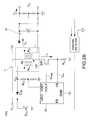
- FIG. 3Ais a circuit block diagram of a PSR according to an embodiment of the present invention.
- the PSR 10comprises a pulse-width-modulation signal generation circuit 12 and a synchronous timing pulse generation circuit 14. Two input terminals of the pulse-width-modulation signal generation circuit 12 are connected to the discharging time detection terminal VDET and the switching current sensing terminal VS of PSR 10 respectively.
- the reflected voltage V wcan be detected through the discharging time detection terminal VDET, and the reflected voltage V w is in response to a secondary side switching current I s .
- the reflected voltage V wwill drop sharply when the secondary side switching current Is drops to zero.
- the pulse-width-modulation signal generation circuit 12can detect the reflected voltage V w through a discharging time detector 202 connected to the discharging time detection terminal VDET, and accordingly output a discharging time signal V DSC corresponding to the secondary side switching current Is.
- the discharging time signal VD SCWhen energy stored in the transformer 100 is released to the secondary side 22, the discharging time signal VD SC is at a high level. Once release of the energy stored in the transformer 100 is accomplished (that is, the secondary side switching current Is drops to zero), the discharging time signal V DSC is at a low level.
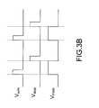
- the pulse-width-modulation signal generation circuit 12firstly outputs an adjusted signal V Mod after performing signal process of an output waveform rebuilding circuit, a filter, an amplifier, and a comparator on the discharging time signal V DSC , the primary side switching current signal Vacs, and a critical voltage V ref2 . And then, further according to a starting pulse V sync from the synchronous timing pulse generation circuit 14, the pulse-width-modulation signal V PWM is output through an SR flip-flop 204. Taking FIG.
- the starting pulse V syncis used to determine the time when the pulse-width-modulation signal V PWM is switched to a high level
- the adjusted signal V Modis used to determine the time when the pulse-width-modulation signal V PWM is switched to a low level.
- the synchronous timing pulse generation circuit 14is used to output the starting pulse V syne of the pulse-width-modulation signal V PWM , and the synchronous timing pulse generation circuit 14 comprises a time delay unit 110, a timing pulse regulation unit 120, and a synchronization control unit 130.
- the time delay unit 110receives the starting pulse V sync , and outputs a control signal TR after delaying the starting pulse V sync for a predetermined time.
- a time period of the predetermined timecan be designed depending on a practical circuit specification.
- the predetermined timecan be 50 ns to 100 ns, or may be set to be larger than a hold time of the SR flip-flop 204.
- the timing pulse regulation unit 120outputs a timing pulse signal T END according to the control signal TR.
- FIG. 4is an internal circuit arrangement diagram of a timing pulse regulation unit according to an embodiment of the present invention.
- the timing pulse regulation unit 120comprises a charging and discharging circuit 300 and a comparator 310.
- the charging and discharging circuit 300comprises a capacitor 302, a switch element 304, a level limiting circuit 306, and a constant current source 320.
- the control signal TRcan be used to control ON or OFF of the switch element 304. For example, when the control signal TR is at a low level and turns off the switch element 304, the circuit 300 can charge the capacitor 302 through the constant current source 320 connected to a power source VCC. While the control signal TR is at a high level (the switch element 304 is ON), the capacitor 302 can be discharged through the switch element 304 connected to ground.
- the level limiting circuit 306can limit a voltage signal to a high level voltage value V H after the charging process, and limit the voltage signal to a low level voltage value V L after the discharging process respectively (that is, a level value of the voltage signal is limited between the highest voltage value V H and the lowest voltage value V L ), and accordingly output an indication signal V tri .
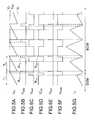
- a timing waveform diagram of the indication signal V triis shown as in FIG. 5A , and the level limiting circuit 306 is not limited to what is shown in FIG. 4 , in which the high level voltage value V H and the low level voltage value V L are limited by two back-to-back connected diodes.
- FIGs. 5A and 5Bare relative timing waveform diagrams of an indication signal V tri and a timing pulse signal T END , which illustrates the operations of an embodiment in which a high level voltage value V H is larger than a reference voltage V refl .
- the reference voltage V refl and the high level voltage value V Hcan also be equal depending on presetting of a user, which is not used to limit the scope of the present invention.
- FIG. 6Ais a function block diagram of a synchronization control unit according to an embodiment of the present invention.
- a synchronization control unit 130comprises an inverter 502 and an AND logic gate 504.
- the inverter 502receives the discharging time signal V DSC , and outputs an inverse discharging time signal V' DSC after inverting the discharging time signal V DSC .
- Two input terminals of the AND logic gate 504receive the inverse discharging time signal V' DSC and the timing pulse signal T END respectively, and accordingly output the starting pulse V sync .
- Relative timing waveform diagrams of the discharging time signal V DSC , the inverse discharging time signal V' DSC , the timing pulse signal T END , and the starting pulse V syncare illustrated in FIGs. 5B to 5E .
- the AND logic gate 504enables the starting pulse V sync to a high level.
- a triggering time of the starting pulse V synccan be synchronized to either the timing pulse signal T END or the inverse discharging time signal V' DSC .
- a rising edge R T1 of the timing pulse signal T ENDoccurs later than a rising edge R v1 , of the inverse discharging time signal V' DSC
- the triggering time of the starting pulse V syncis synchronized to the rising edge R T1 of the timing pulse signal TEND (that is, the later one).
- a second period T 2even if a rising edge R T2 of the timing pulse signal TEND occurs earlier than a rising edge R v2 of the inverse discharging time signal V' DSC , the triggering time of the starting pulse V sync is synchronized to the rising edge R V2 of the inverse discharging time signal V' DSC (that is, also the later one).
- the triggering time of the starting pulse V synccan be selectively synchronized to one occurring later of the rising edge of the timing pulse signal TEND and the rising edge of the inverse discharging time signal V' DSC (that is, a falling edge of the discharging time signal V DSC ) in the same period.
- the starting pulse V syncis used to determine a pulse starting time of the pulse-width-modulation signal V PWM (that is, the time when the pulse-width-modulation signal V PWM is switched to a high level), so as shown in FIG. 5F , the pulse starting time of the pulse-width-modulation signal V PWM can also be synchronized to one occurring later of the rising edge of the timing pulse signal TEND and the rising edge of the inverse discharging time signal V' DSC in the same period, thereby achieving a purpose of modulating the pulse starting time of the pulse-width-modulation signal V PWM .
- the high level and the low level of the pulse-width-modulation signal V PWMare used to switch the transistor SW, so as to control a power to be input or not input to the primary side 11 (that is, to generate or not generate the primary side switching current Ip).
- the primary side switching current Ipis not formed immediately until the pulse-width-modulation signal V PWM is triggered, therefore forming a Discontinuous Conduction Mode (DCM) of the primary side switching current Ip.
- DCMDiscontinuous Conduction Mode
- the pulse starting time (that is, a triggering point of the starting pulse V sync ) of the pulse-width-modulation signal V PWMis adjusted to be synchronized to the falling edge of the discharging time signal V DSC (that is, the rising edge of the inverse discharging time signal V' DSC ).
- the switching power supplycan effectively and immediately switches back to be charged at the primary side (to form the primary side switching current Ip), so as to form a Boundary Conduction Mode (BCM) and prevent the inductor current passing through the primary side winding Np from entering the CCM.
- BCMBoundary Conduction Mode
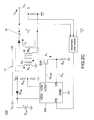
- FIG. 3Cis a circuit block diagram of a PSR according to another embodiment of the present invention.
- the discharging time detection terminal VDETcan also be connected to a valley detector 206, and the valley detector 206 can detect the reflected voltage V w through the discharging time detection terminal VDET, and accordingly output a valley signal V VLY , so as to determine the lowest point of resonance during turn-off interval of the transistor SW.
- the synchronous timing pulse generation circuit 14can perform signal process of time delay, timing pulse regulation, and synchronization control according to the valley signal V VLY and the starting pulse V sync , so as to modulate the pulse starting time of the pulse-width-modulation signal V PWM (that is, the starting pulse V sync ).
- the valley detector 206is applied to the synchronous timing pulse generation circuit 14 according to the embodiment of the present invention, so as to not only achieve the purpose of modulating the starting pulse V sync , but also reduce switching loss of the transistor SW (that is, the transistor SW is limited only to be conducted at its valley and thereby its highest frequency is also limited), and reduce electromagnetic interference (EMI) of the converter.
- EMIelectromagnetic interference
- FIG. 6Bis an internal circuit arrangement diagram of a synchronization control unit according to a second embodiment of the present invention.
- a synchronization control unit 130acan further comprise a one shot circuit 506, an SR flip-flop 508, and a time delay unit 510.
- the one shot circuit 506receives the timing pulse signal T END , and accordingly converts it to obtain a one shot timing pulse signal V OS .
- Two input terminals of the SR flip-flop 508are connected to output terminals of the one shot circuit 506 and the time delay unit 510 respectively.
- the time delay unit 510delays the starting pulse V sync for a predetermined time, and then outputs the delayed signal to the SR flip-flop 508.
- the SR flip-flop 508receives the one shot timing pulse signal V OS and the starting pulse V sync after being delayed for the predetermined time, and accordingly generates the timing pulse signal T END , so as to allow the AND logic gate 504 to accordingly output the starting pulse V sync subsequently.
- FIG. 7is a circuit block diagram of a synchronous timing pulse generation circuit according to a third embodiment of the present invention.
- the starting pulse V sync received by the time delay unit 110 of a synchronous timing pulse generation circuit 14acan also be generated after a pulse-width-modulation signal V PWM processed by a one shot circuit 140. That is to say, a practical connection manner in which the time delay unit 110 is electrically connected to other external circuits is not used to limit the scope of the present invention.
- the time delay unit 110receives the starting pulse V sync of the pulse-width-modulation signal V PWM , so that a timing pulse regulation unit 120 and a synchronization control unit 130 perform subsequent signal process, so as to enable the starting pulse V sync to be synchronized to the later-occurring rising edge of either a timing pulse signal T END or an inverse discharging time signal V' DSC in the same period, without deteriorating the generality of the present invention.
- FIG. 8Ais a circuit block diagram of an application architecture of a voltage mode control PSR including a synchronous timing pulse generation circuit 14 according to a fourth embodiment of the present invention.
- FIGs. 8B and 8Care circuit block diagrams of a voltage mode control SSR and of a current mode control SSR including a synchronous timing pulse generation circuit 14 respectively according to a fifth embodiment and a sixth embodiment of the present invention.
- the synchronous timing pulse generation circuit according to the embodiment of the present inventioncan selectively be arranged in a PSR or a SSR without being limited to the constant voltage mode or constant current mode.
- the synchronous timing pulse generation circuitis applied to the circuit regulator of the switching power supply, so as to further control and output the pulse-width-modulation signal with the pulse starting time capable of being modulated, thereby preventing the inductor current of the switching power supply from entering the CCM.
Landscapes
- Engineering & Computer Science (AREA)
- Power Engineering (AREA)
- Dc-Dc Converters (AREA)
Abstract
Description
- The present invention relates to a circuit regulator and a synchronous timing pulse generation circuit thereof, and more particularly to a circuit regulator and a synchronous timing pulse generation circuit thereof, capable of synchronously controlling a pulse starting time of a pulse-width-modulation signal, and preventing an inductor current from entering a Continuous Conduction Mode (CCM).
- Now, power supplies are not only required to provide stable output voltages and output currents for various electronic devices, but also required to satisfy the requirements of electronic devices on safety regulations. According to the design techniques, power supplies can be categorized into linear power supplies and switching power supplies. However, the linear power supply needs large and heavy isolation transformers and also large capacitors for regulation, which results in problems of larger volume and heavier weight. A worse part is that the linear power supply has excessively low conversion efficiency. Hence, at a practical application level, as compared with the linear power supply, a switching power supply formed by smaller power electronic switches, a lighter isolation transformer, a smaller capacitor, and a diode has better industrial applicability and is mostly used.
- Generally, a working frequency of the switching power supply is between 20 KHz and 100 KHz. If it is used in cooperation with a Zero Voltage Switching (ZVS), a switching frequency can be further increased to be higher than 200 KHz, so as to obtain smaller and lighter design with higher power transfer efficiency and even high power factor in AC/DC applications.
- However, the switching power supply has more complex operation modes. While an unexpected operation happens, the circuit may enter an unexpected operation mode and let the converter fail to keep output current constant. For example,
FIG. 1 is a brief circuit architecture view of a conventional switching power supply. When the switching power supply transfers the power from a primary side to a secondary side by performing the charging and discharging processes of magnetic core of the isolation transformer through the magnetic inductor L, the switching power supply generates a primary side switching current Ip and a secondary side switching current Is respectively at two sides of the transformer. When the primary side switching current Ip enters a CCM on the inductor L under improper control, it is very easy to result in successive accumulation of the inductor current in the charging and discharging processes of the transformer, so as to cause a problem of magnetic core saturation. In this situation, the core power loss will increase. This may also cause high switching current and higher switching loss of switching transistor and diodes. Consequently, additional power consumption of the switching power supply will be cost. Particularly, it is more difficult for the converter using primary side control to obtain an accurate and stable constant output current when undergoing the CCM. - In view of the foregoing, the present invention is a multi-purpose synchronous timing pulse generation circuit which can be applicable to switching power supplies for improving the performance of the converter. The synchronous timing pulse generation circuit controls pulse starting time of the pulse-width-modulation signal after performing certain signal process including time delay, timing pulse regulation, and pulse-width-modulation signal synchronization control triggered by both of the discharging time signal of the secondary side and the timing pulse signal. Besides, through the circuit regulator and the synchronous timing pulse generation circuit thereof, an inductor current of the switching power supply is effectively prevented from entering a CCM.
- The present invention provides a synchronous timing pulse generation circuit, applicable to a switching power supply which uses a pulse-width-modulation signal to determine the conducting time of power switch. In such application, the switching power supply has a primary side and a secondary side, and the switching power supply enables a power to be selectively input or not input to the primary side through the pulse-width-modulation signal. The synchronous timing pulse generation circuit is used to generate a starting pulse of the pulse-width-modulation signal, and the synchronous timing pulse generation circuit comprises a time delay unit, a timing pulse regulation unit, and a synchronous control unit.
- The time delay unit outputs a control signal after delaying the starting pulse for a predetermined time. The timing pulse regulation unit enables a constant current source to selectively charge the timing pulse regulation unit according to the control signal, and accordingly outputs a timing pulse signal. The synchronization control unit outputs the starting pulse according to a discharging time signal of the secondary side and the timing pulse signal. By detecting a rising edge of the timing pulse signal and a falling edge of the discharging time signal, a triggering time of the starting pulse is synchronized to one occurring later of the rising edge of the timing pulse signal and the falling edge of the discharging time signal in the same period, and the starting pulse is used to determine a pulse starting time of the pulse-width-modulation signal.
- A circuit regulator is applicable to a switching power supply, wherein the switching power supply has a primary side and a secondary side, and the switching power supply enables a power to be selectively input or not input to the primary side through a pulse-width-modulation signal. The circuit regulator comprises a pulse-width-modulation signal generation circuit and a synchronous timing pulse generation circuit.
- The pulse-width-modulation signal generation circuit outputs the pulse-width-modulation signal according to a primary side switching current signal of the primary side and a discharging time signal of the secondary side. The pulse-width-modulation signal has a starting pulse. The synchronous timing pulse generation circuit outputs the starting pulse after performing signal process of time delay, timing pulse regulation, and synchronization control on the pulse-width-modulation signal and the discharging time signal. The starting pulse is used to determine a pulse starting time of the pulse-width-modulation signal.
- Thus, the circuit regulator and the synchronous timing pulse generation circuit thereof according to the present invention is applied to the switching power supply, such that the pulse starting time of the pulse-width-modulation signal is determined by both the discharging time signal of the secondary side and the timing pulse signal. Through the circuit regulator and the synchronous timing pulse generation circuit thereof according to the present invention, the inductor current of the switching power supply is prevented from entering the CCM.
- The present invention will become more fully understood from the detailed description given herein below for illustration only, and thus are not limitative of the present invention, and wherein:
FIG. 1 is a brief circuit architectural view of a conventional switching power supply;FIG. 2A is a schematic view of an application architecture of a synchronous timing pulse generation circuit applied to a Primary Side Regulator (PSR) according to an embodiment of the present invention;FIG. 2B is a schematic view of an application architecture of a synchronous timing pulse generation circuit applied to a Secondary Side Regulator (SSR) under constant voltage control according to an embodiment of the present invention;FIG. 2C is a schematic view of an application architecture of a synchronous timing pulse generation circuit applied to a Secondary Side Regulator (SSR) under constant current control according to an embodiment of the present invention;FIG. 3A is a circuit block diagram of a PSR according to an embodiment of the present invention;FIG. 3B is a relative timing diagram of a starting pulse, an adjusted signal, and a pulse-width-modulation signal according to an embodiment of the present invention;FIG. 3C is a circuit block diagram of a PSR according to another embodiment of the present invention;FIG. 4 is an internal circuit arrangement diagram of a timing pulse regulation unit according to an embodiment of the present invention;FIGs. 5A to 5G are relative timing waveform diagrams of each terminal of a synchronous timing pulse generation circuit according to an embodiment of the present invention;FIG. 6A is an internal circuit arrangement diagram of a synchronization control unit according to an embodiment of the present invention;FIG. 6B is an internal circuit arrangement diagram of a synchronization control unit according to a second embodiment of the present invention;FIG. 7 is a circuit block diagram of a synchronous timing pulse generation circuit according to a third embodiment of the present invention;FIG. 8A is a circuit block diagram of an application architecture of a voltage mode control PSR including a synchronous timing pulse generation circuit according to a fourth embodiment of the present invention;FIG. 8B is a circuit block diagram of an application architecture of a voltage mode SSR including a synchronous timing pulse generation circuit according to a fifth embodiment of the present invention; andFIG. 8C is a circuit block diagram of an application architecture of a current mode SSR including a synchronous timing pulse generation circuit according to a sixth embodiment of the present invention.FIGs. 2A to 2C are respectively schematic views of application architectures of a synchronous timing pulse generation circuit according to an embodiment of the present invention. The synchronous timing pulse generation circuit according to an embodiment of the present invention can be applied to aprimary side 11 or asecondary side 22 of a switchingpower supply 1000. InFIG. 2A , the synchronous timing pulse generation circuit is applied to a Primary Side Regulator (PSR) 10. InFIGs. 2B and2C , the synchronous timing pulse generation circuit is respectively applied to an Secondary Side Regulator (SSR) 20 under constant voltage control and to anSSR 20a under constant current control.- The switching
power supply 1000 can be, but is not limited to, a flyback converter, a forward converter, a half-bridge converter, a full-bridge converter, or a push-pull converter. - In the following implementation manner, the synchronous timing pulse generation circuit applied to the
PSR 10 is used as an illustration for an embodiment, and is not used to limit the scope of the present invention. - The
PSR 10 is disposed at theprimary side 11 of the switchingpower supply 1000, and the switchingpower supply 1000 has an output voltage Vo, an output current Io, and an input voltage Vin. - A
transformer 100 comprises an auxiliary winding NA, a primary side winding Np, and a secondary side winding Ns. Theprimary side 11 is commonly grounded at a grounding terminal of the input voltage Vin, while thesecondary side 22 is commonly grounded at a grounding terminal of the output voltage Vo. - The
PSR 10 has a power source supply terminal VDD, a grounding terminal GND, an output terminal VOUT, a discharging time detection terminal VDET, and a switching current sensing terminal VS. ThePSR 10 can detect a reflected voltage Vw through the discharging time detection terminal VDET, a primary side switching current signal Vcs corresponding to a primary side switching current Ip through the switching current sensing terminal VS, and accordingly output a pulse-width-modulation signal Vpwm. - The pulse-width-modulation signal Vpwm is connected to a gate of a transistor SW through the output terminal VOUT. Hence, the
PSR 10 can switch the transistor SW through the pulse-width-modulation signal Vpwm, so as to control a power to be input or not input to theprimary side 11. The primary side switching current signal Vcs can be a magnetizing current signal. The reflected voltage Vw can charge a capacitor CDD through a rectifier DDD and provide energy to thePSR 10. FIG. 3A is a circuit block diagram of a PSR according to an embodiment of the present invention. ThePSR 10 comprises a pulse-width-modulationsignal generation circuit 12 and a synchronous timingpulse generation circuit 14. Two input terminals of the pulse-width-modulationsignal generation circuit 12 are connected to the discharging time detection terminal VDET and the switching current sensing terminal VS ofPSR 10 respectively. Referring toFIGs. 2A and3A , the reflected voltage Vw can be detected through the discharging time detection terminal VDET, and the reflected voltage Vw is in response to a secondary side switching current Is. The reflected voltage Vw will drop sharply when the secondary side switching current Is drops to zero. Thus, the pulse-width-modulationsignal generation circuit 12 can detect the reflected voltage Vw through a dischargingtime detector 202 connected to the discharging time detection terminal VDET, and accordingly output a discharging time signal VDSC corresponding to the secondary side switching current Is.- When energy stored in the
transformer 100 is released to thesecondary side 22, the discharging time signal VDSC is at a high level. Once release of the energy stored in thetransformer 100 is accomplished (that is, the secondary side switching current Is drops to zero), the discharging time signal VDSC is at a low level. - As shown in
FIG. 3A , the pulse-width-modulationsignal generation circuit 12 firstly outputs an adjusted signal VMod after performing signal process of an output waveform rebuilding circuit, a filter, an amplifier, and a comparator on the discharging time signal VDSC, the primary side switching current signal Vacs, and a critical voltage Vref2. And then, further according to a starting pulse Vsync from the synchronous timingpulse generation circuit 14, the pulse-width-modulation signal VPWM is output through an SR flip-flop 204. TakingFIG. 3B as an example, the starting pulse Vsync is used to determine the time when the pulse-width-modulation signal VPWM is switched to a high level, while the adjusted signal VMod is used to determine the time when the pulse-width-modulation signal VPWM is switched to a low level. - The synchronous timing
pulse generation circuit 14 is used to output the starting pulse Vsyne of the pulse-width-modulation signal VPWM, and the synchronous timingpulse generation circuit 14 comprises atime delay unit 110, a timingpulse regulation unit 120, and asynchronization control unit 130. Thetime delay unit 110 receives the starting pulse Vsync, and outputs a control signal TR after delaying the starting pulse Vsync for a predetermined time. A time period of the predetermined time can be designed depending on a practical circuit specification. For example, the predetermined time can be 50 ns to 100 ns, or may be set to be larger than a hold time of the SR flip-flop 204. - The timing
pulse regulation unit 120 outputs a timing pulse signal TEND according to the control signal TR.FIG. 4 is an internal circuit arrangement diagram of a timing pulse regulation unit according to an embodiment of the present invention. The timingpulse regulation unit 120 comprises a charging and dischargingcircuit 300 and acomparator 310. The charging and dischargingcircuit 300 comprises acapacitor 302, aswitch element 304, alevel limiting circuit 306, and a constantcurrent source 320. - The control signal TR can be used to control ON or OFF of the
switch element 304. For example, when the control signal TR is at a low level and turns off theswitch element 304, thecircuit 300 can charge thecapacitor 302 through the constantcurrent source 320 connected to a power source VCC. While the control signal TR is at a high level (theswitch element 304 is ON), thecapacitor 302 can be discharged through theswitch element 304 connected to ground. Thelevel limiting circuit 306 can limit a voltage signal to a high level voltage value VH after the charging process, and limit the voltage signal to a low level voltage value VL after the discharging process respectively (that is, a level value of the voltage signal is limited between the highest voltage value VH and the lowest voltage value VL), and accordingly output an indication signal Vtri. A timing waveform diagram of the indication signal Vtri is shown as inFIG. 5A , and thelevel limiting circuit 306 is not limited to what is shown inFIG. 4 , in which the high level voltage value VH and the low level voltage value VL are limited by two back-to-back connected diodes. - After receiving the indication signal Vtri, the
comparator 310 compares the indication signal Vtri with a reference voltage Vrefi , and accordingly outputs the timing pulse signal TEND· The high level voltage value VH, the low level voltage value VL, and the reference voltage Vrefl can also be designed in a self actuated way depending on a practical circuit specification.FIGs. 5A and 5B are relative timing waveform diagrams of an indication signal Vtri and a timing pulse signal TEND, which illustrates the operations of an embodiment in which a high level voltage value VH is larger than a reference voltage Vrefl. However, the reference voltage Vrefl and the high level voltage value VH can also be equal depending on presetting of a user, which is not used to limit the scope of the present invention. FIG. 6A is a function block diagram of a synchronization control unit according to an embodiment of the present invention. Asynchronization control unit 130 comprises aninverter 502 and an ANDlogic gate 504. Theinverter 502 receives the discharging time signal VDSC, and outputs an inverse discharging time signal V'DSC after inverting the discharging time signal VDSC. Two input terminals of the ANDlogic gate 504 receive the inverse discharging time signal V'DSC and the timing pulse signal TEND respectively, and accordingly output the starting pulse Vsync. Relative timing waveform diagrams of the discharging time signal VDSC, the inverse discharging time signal V'DSC, the timing pulse signal TEND, and the starting pulse Vsync, are illustrated inFIGs. 5B to 5E .- Accordingly, in other words, only when both the inverse discharging time signal V'DSC and the timing pulse signal TEND are at a high level, the AND
logic gate 504 enables the starting pulse Vsync to a high level. Hence, a triggering time of the starting pulse Vsync can be synchronized to either the timing pulse signal TEND or the inverse discharging time signal V'DSC. - More specifically, taking a first period T1 as an example, when a rising edge RT1 of the timing pulse signal TEND occurs later than a rising edge Rv1, of the inverse discharging time signal V'DSC, the triggering time of the starting pulse Vsync is synchronized to the rising edge RT1 of the timing pulse signal TEND (that is, the later one). As for a second period T2, even if a rising edge RT2 of the timing pulse signal TEND occurs earlier than a rising edge Rv2 of the inverse discharging time signal V'DSC, the triggering time of the starting pulse Vsync is synchronized to the rising edge RV2 of the inverse discharging time signal V'DSC (that is, also the later one). It can be known from the foregoing that, in the
synchronization control unit 130 according to an embodiment of the present invention, the triggering time of the starting pulse Vsync can be selectively synchronized to one occurring later of the rising edge of the timing pulse signal TEND and the rising edge of the inverse discharging time signal V'DSC (that is, a falling edge of the discharging time signal VDSC) in the same period. - In view of the foregoing, the starting pulse Vsync is used to determine a pulse starting time of the pulse-width-modulation signal VPWM (that is, the time when the pulse-width-modulation signal VPWM is switched to a high level), so as shown in
FIG. 5F , the pulse starting time of the pulse-width-modulation signal VPWM can also be synchronized to one occurring later of the rising edge of the timing pulse signal TEND and the rising edge of the inverse discharging time signal V'DSC in the same period, thereby achieving a purpose of modulating the pulse starting time of the pulse-width-modulation signal VPWM. - Referring to
FIG. 2A , the high level and the low level of the pulse-width-modulation signal VPWM are used to switch the transistor SW, so as to control a power to be input or not input to the primary side 11 (that is, to generate or not generate the primary side switching current Ip). Hence, referring toFIGs. 5C, 5F, and 5G , during the first period T1, even if the discharging time signal VDSC returns to the low level (that is, the secondary side switching current Is returns to the zero point), the primary side switching current Ip is not formed immediately until the pulse-width-modulation signal VPWM is triggered, therefore forming a Discontinuous Conduction Mode (DCM) of the primary side switching current Ip. - Next, according to the embodiment of the present invention, referring to
FIGs. 5A to 5G , after the second period T2, the pulse starting time (that is, a triggering point of the starting pulse Vsync) of the pulse-width-modulation signal VPWM is adjusted to be synchronized to the falling edge of the discharging time signal VDSC (that is, the rising edge of the inverse discharging time signal V'DSC). Hence, after discharging at the secondary side is accomplished, the switching power supply can effectively and immediately switches back to be charged at the primary side (to form the primary side switching current Ip), so as to form a Boundary Conduction Mode (BCM) and prevent the inductor current passing through the primary side winding Np from entering the CCM. - Next, referring to
FIGs. 2A and3C, FIG. 3C is a circuit block diagram of a PSR according to another embodiment of the present invention. The discharging time detection terminal VDET can also be connected to avalley detector 206, and thevalley detector 206 can detect the reflected voltage Vw through the discharging time detection terminal VDET, and accordingly output a valley signal VVLY, so as to determine the lowest point of resonance during turn-off interval of the transistor SW. Hence, the synchronous timingpulse generation circuit 14 can perform signal process of time delay, timing pulse regulation, and synchronization control according to the valley signal VVLY and the starting pulse Vsync, so as to modulate the pulse starting time of the pulse-width-modulation signal VPWM (that is, the starting pulse Vsync). Thevalley detector 206 is applied to the synchronous timingpulse generation circuit 14 according to the embodiment of the present invention, so as to not only achieve the purpose of modulating the starting pulse Vsync, but also reduce switching loss of the transistor SW (that is, the transistor SW is limited only to be conducted at its valley and thereby its highest frequency is also limited), and reduce electromagnetic interference (EMI) of the converter. FIG. 6B is an internal circuit arrangement diagram of a synchronization control unit according to a second embodiment of the present invention. Besides theinverter 502 and the ANDlogic gate 504, asynchronization control unit 130a can further comprise a oneshot circuit 506, an SR flip-flop 508, and atime delay unit 510.- The one
shot circuit 506 receives the timing pulse signal TEND, and accordingly converts it to obtain a one shot timing pulse signal VOS. Two input terminals of the SR flip-flop 508 are connected to output terminals of the oneshot circuit 506 and thetime delay unit 510 respectively. Thetime delay unit 510 delays the starting pulse Vsync for a predetermined time, and then outputs the delayed signal to the SR flip-flop 508. Hence, the SR flip-flop 508 receives the one shot timing pulse signal VOS and the starting pulse Vsync after being delayed for the predetermined time, and accordingly generates the timing pulse signal TEND, so as to allow the ANDlogic gate 504 to accordingly output the starting pulse Vsync subsequently. - Next,
FIG. 7 is a circuit block diagram of a synchronous timing pulse generation circuit according to a third embodiment of the present invention. The starting pulse Vsync received by thetime delay unit 110 of a synchronous timingpulse generation circuit 14a can also be generated after a pulse-width-modulation signal VPWM processed by a oneshot circuit 140. That is to say, a practical connection manner in which thetime delay unit 110 is electrically connected to other external circuits is not used to limit the scope of the present invention. The cases in which according to the embodiment of the present invention, thetime delay unit 110 receives the starting pulse Vsync of the pulse-width-modulation signal VPWM, so that a timingpulse regulation unit 120 and asynchronization control unit 130 perform subsequent signal process, so as to enable the starting pulse Vsync to be synchronized to the later-occurring rising edge of either a timing pulse signal TEND or an inverse discharging time signal V'DSC in the same period, without deteriorating the generality of the present invention. FIG. 8A is a circuit block diagram of an application architecture of a voltage mode control PSR including a synchronous timingpulse generation circuit 14 according to a fourth embodiment of the present invention.FIGs. 8B and8C are circuit block diagrams of a voltage mode control SSR and of a current mode control SSR including a synchronous timingpulse generation circuit 14 respectively according to a fifth embodiment and a sixth embodiment of the present invention. Thus, the synchronous timing pulse generation circuit according to the embodiment of the present invention can selectively be arranged in a PSR or a SSR without being limited to the constant voltage mode or constant current mode.- Next, the synchronous timing pulse generation circuit according to the embodiment of the present invention is applied to the circuit regulator of the switching power supply, so as to further control and output the pulse-width-modulation signal with the pulse starting time capable of being modulated, thereby preventing the inductor current of the switching power supply from entering the CCM.
Claims (11)
- A synchronous timing pulse generation circuit, applicable to a switching power supply, wherein the switching power supply has a primary side and a secondary side, the switching power supply enables a power to be selectively input or not input to the primary side through a pulse-width-modulation signal, the synchronous timing pulse generation circuit is used to generate a starting pulse of the pulse-width-modulation signal, the synchronous timing pulse generation circuit comprising:a time delay unit, for outputting a control signal after delaying the starting pulse for a predetermined time;a timing pulse regulation unit, for enabling a constant current source to selectively charge the timing pulse regulation unit according to the control signal, and accordingly outputting a timing pulse signal; anda synchronization control unit, for outputting the starting pulse according to a discharging time signal of the secondary side and the timing pulse signal, wherein the timing pulse signal has a rising edge, the discharging time signal has a falling edge, a triggering time of the starting pulse is synchronized to one occurring later of the rising edge of the timing pulse signal and the falling edge of the discharging time signal in the same period, and the starting pulse is used to determine a pulse starting time of the pulse-width-modulation signal.
- The synchronous timing pulse generation circuit according to claim 1, wherein the timing pulse regulation unit comprises:a charging and discharging circuit, for outputting an indication signal according to the control signal and the constant current source; anda comparator, for comparing the indication signal with a reference voltage, and accordingly outputting the timing pulse signal.
- The synchronous timing pulse generation circuit according to claim 2, wherein the charging and discharging circuit comprises:a capacitor, connected between the constant current source and a ground;a switch element, electrically connected between the capacitor and the ground, wherein ON or OFF of the switch element is controlled by the control signal, so as to control whether the constant current source charges the capacitor; anda level limiting circuit, for limiting a level of a signal output by the capacitor, so as to output the indication signal.
- The synchronous timing pulse generation circuit according to claim 1, wherein the synchronization control unit comprises:an inverter, for receiving the discharging time signal, and outputting an inverse discharging time signal; andan AND logic gate, for receiving the timing pulse signal and the inverse discharging time signal, and accordingly outputting the starting pulse.
- The synchronous timing pulse generation circuit according to claim 4, wherein the synchronization control unit further comprises:a one shot circuit, for receiving the timing pulse signal, and outputting a one shot timing pulse signal;the time delay unit, for outputting the control signal after delaying the starting pulse for the predetermined time; anda flip-flop, for receiving the one shot timing pulse signal and the control signal, and accordingly outputting the timing pulse signal.
- A circuit regulator, applicable to a switching power supply, wherein the switching power supply has a primary side and a secondary side, the switching power supply enables a power to be selectively input or not input to the primary side through a pulse-width-modulation signal, the circuit regulator comprising:a pulse-width-modulation signal generation circuit, for outputting the pulse-width-modulation signal according to a primary side switching current signal of the primary side and a discharging time signal of the secondary side, wherein the pulse-width-modulation signal has a starting pulse; anda synchronous timing pulse generation circuit, for outputting the starting pulse after performing signal process of time delay, timing pulse regulation, and synchronization control on the pulse-width-modulation signal and the discharging time signal, wherein the starting pulse is used to determine a pulse starting time of the pulse-width-modulation signal.
- The circuit regulator according to claim 6, wherein the synchronous timing pulse generation circuit comprises:a time delay unit, for receiving the starting pulse, and outputting a control signal after delaying the starting pulse for a predetermined time;a timing pulse regulation unit, for enabling a constant current source to selectively charge the timing pulse regulation unit according to the control signal, and accordingly outputting a timing pulse signal; anda synchronization control unit, for outputting the starting pulse according to the discharging time signal and the timing pulse signal, wherein the timing pulse signal has a rising edge, the discharging time signal has a falling edge, and a triggering time of the starting pulse is synchronized to one occurring later of the rising edge of the timing pulse signal and the falling edge of the discharging time signal in the same period.
- The circuit regulator according to claim 7, wherein the timing pulse regulation unit comprises:a charging and discharging circuit, for outputting an indication signal according to the control signal and the constant current source; anda comparator, for comparing the indication signal with a reference voltage, and accordingly outputting the timing pulse signal.
- The circuit regulator according to claim 8, wherein the charging and discharging circuit comprises:a capacitor, connected between the constant current source and a ground;a switch element, electrically connected between the capacitor and the ground, wherein ON or OFF of the switch element is controlled by the control signal, so as to control whether the constant current source charges the capacitor; anda level limiting circuit, for limiting a level of a signal output by the capacitor, so as to output the indication signal.
- The circuit regulator according to claim 7, wherein the synchronization control unit comprises:an inverter, for receiving the discharging time signal, and outputting an inverse discharging time signal; andan AND logic gate, for receiving the timing pulse signal and the inverse discharging time signal, and accordingly outputting the starting pulse.
- The circuit regulator according to claim 10, wherein the synchronization control unit further comprises:a one shot circuit, for receiving the timing pulse signal, and outputting a one shot timing pulse signal;the time delay unit, for outputting the control signal after delaying the starting pulse for the predetermined time; anda flip-flop, for receiving the one shot timing pulse signal and the control signal, and accordingly outputting the timing pulse signal.
Applications Claiming Priority (1)
| Application Number | Priority Date | Filing Date | Title |
|---|---|---|---|
| TW099125990ATWI419469B (en) | 2010-08-04 | 2010-08-04 | Regulator and synchronized pulse generator thereof |
Publications (3)
| Publication Number | Publication Date |
|---|---|
| EP2416474A2true EP2416474A2 (en) | 2012-02-08 |
| EP2416474A3 EP2416474A3 (en) | 2014-10-29 |
| EP2416474B1 EP2416474B1 (en) | 2017-12-27 |
Family
ID=45002186
Family Applications (1)
| Application Number | Title | Priority Date | Filing Date |
|---|---|---|---|
| EP10195113.5AActiveEP2416474B1 (en) | 2010-08-04 | 2010-12-15 | Circuit regulator and synchronous timing pulse generation circuit thereof |
Country Status (6)
| Country | Link |
|---|---|
| US (1) | US8422253B2 (en) |
| EP (1) | EP2416474B1 (en) |
| JP (1) | JP5181014B2 (en) |
| KR (1) | KR101121300B1 (en) |
| ES (1) | ES2661843T3 (en) |
| TW (1) | TWI419469B (en) |
Cited By (1)
| Publication number | Priority date | Publication date | Assignee | Title |
|---|---|---|---|---|
| CN109361500A (en)* | 2018-10-25 | 2019-02-19 | 南通先进通信技术研究院有限公司 | A method of the plesiochronous external pulse of self-correcting based on chip |
Families Citing this family (15)
| Publication number | Priority date | Publication date | Assignee | Title |
|---|---|---|---|---|
| EP2445098B1 (en)* | 2010-10-25 | 2019-08-07 | STMicroelectronics Srl | Control device for a resonant converter. |
| MX2012013946A (en)* | 2011-12-01 | 2013-06-17 | Rab Lighting Inc | Led driver protection circuit. |
| TWI444102B (en)* | 2012-05-30 | 2014-07-01 | Macroblock Inc | Driving circuit for led |
| US8665612B2 (en)* | 2012-07-10 | 2014-03-04 | Immense Advance Technology Corporation | Constant current controller |
| JP5814876B2 (en) | 2012-07-27 | 2015-11-17 | 株式会社東芝 | Synchronous rectification type power supply circuit and adjustment method thereof |
| US9197124B2 (en)* | 2012-10-24 | 2015-11-24 | Marvell World Trade Ltd. | Method and apparatus to reduce overcurrent during the startup of a switching regulator |
| TWI488414B (en)* | 2012-10-30 | 2015-06-11 | Lite On Technology Corp | A flyback voltage converter with primary side feedback controlling and a voltage controlling method thereof |
| SG11201502947UA (en) | 2013-10-28 | 2015-06-29 | Advanced Charging Technologies Llc | Electrical circuit for powering consumer electronic devices |
| CN104702130B (en)* | 2013-12-05 | 2017-05-03 | 立锜科技股份有限公司 | Control circuit of power supply conversion circuit |
| US9762132B2 (en) | 2014-10-28 | 2017-09-12 | Advanced Charging Technologies, LLC | Electrical circuit for delivering power to consumer electronic devices |
| TWI575854B (en)* | 2015-01-08 | 2017-03-21 | 群光電能科技股份有限公司 | Speedydischarging circuit and power supply apparatus with speedydischarging circuit |
| EP3666735A1 (en)* | 2018-12-14 | 2020-06-17 | ABB Schweiz AG | Dielectric barrier discharge for ballast water treatment using optimized voltage shape control |
| CN111880038B (en)* | 2020-08-07 | 2022-04-01 | 广东电网有限责任公司 | Secondary circuit proofreading device |
| TWI740676B (en) | 2020-10-12 | 2021-09-21 | 財團法人工業技術研究院 | Pulse-width modulation signal observation circuit and hardware-in-the-loop simulation device having the same |
| US11962247B2 (en)* | 2021-02-25 | 2024-04-16 | Richtek Technology Corporation | Resonant half-bridge flyback power converter with skipping cycles and control method thereof |
Family Cites Families (14)
| Publication number | Priority date | Publication date | Assignee | Title |
|---|---|---|---|---|
| US4870555A (en)* | 1988-10-14 | 1989-09-26 | Compaq Computer Corporation | High-efficiency DC-to-DC power supply with synchronous rectification |
| US6650552B2 (en)* | 2001-05-25 | 2003-11-18 | Tdk Corporation | Switching power supply unit with series connected converter circuits |
| JP3488709B2 (en)* | 2001-12-12 | 2004-01-19 | 株式会社東芝 | Switching power supply |
| US6836415B1 (en)* | 2003-06-18 | 2004-12-28 | Systems General Corp. | Primary-side regulated pulse width modulation controller with improved load regulation |
| US6980441B2 (en)* | 2003-07-28 | 2005-12-27 | Astec International Limited | Circuit and method for controlling a synchronous rectifier in a power converter |
| JP4733186B2 (en) | 2005-10-09 | 2011-07-27 | システム ジェネラル コーポレーション | Switching control circuit with variable switching frequency for a power converter with controlled primary side |
| GB2438464A (en)* | 2006-05-23 | 2007-11-28 | Cambridge Semiconductor Ltd | Regulating the output of a switch mode power supply |
| TWI314808B (en)* | 2006-09-06 | 2009-09-11 | Delta Electronics Inc | Resonance converter and driving method for synchronous rectifier thereof |
| US20080062725A1 (en)* | 2006-09-11 | 2008-03-13 | Ta-Yung Yang | Multi-channels power converter having power saving means to improve light load efficiency |
| JP4806333B2 (en)* | 2006-11-09 | 2011-11-02 | 本田技研工業株式会社 | DC-DC converter |
| JP2009071997A (en)* | 2007-09-13 | 2009-04-02 | Panasonic Electric Works Co Ltd | Power converter and vehicular lamp |
| US7983061B2 (en)* | 2008-02-22 | 2011-07-19 | System General Corporation | Switching controller capable of reducing acoustic noise for power converters |
| JP5165454B2 (en)* | 2008-05-14 | 2013-03-21 | 株式会社ダイヘン | Power supply |
| WO2010083511A1 (en)* | 2009-01-19 | 2010-07-22 | Flextronics International Usa, Inc. | Controller for a power converter |
- 2010
- 2010-08-04TWTW099125990Apatent/TWI419469B/enactive
- 2010-12-15EPEP10195113.5Apatent/EP2416474B1/enactiveActive
- 2010-12-15ESES10195113.5Tpatent/ES2661843T3/enactiveActive
- 2010-12-16USUS12/970,029patent/US8422253B2/enactiveActive
- 2010-12-17JPJP2010282090Apatent/JP5181014B2/enactiveActive
- 2010-12-23KRKR1020100133814Apatent/KR101121300B1/enactiveActive
Non-Patent Citations (1)
| Title |
|---|
| None |
Cited By (1)
| Publication number | Priority date | Publication date | Assignee | Title |
|---|---|---|---|---|
| CN109361500A (en)* | 2018-10-25 | 2019-02-19 | 南通先进通信技术研究院有限公司 | A method of the plesiochronous external pulse of self-correcting based on chip |
Also Published As
| Publication number | Publication date |
|---|---|
| KR101121300B1 (en) | 2012-03-20 |
| JP2012039844A (en) | 2012-02-23 |
| JP5181014B2 (en) | 2013-04-10 |
| ES2661843T3 (en) | 2018-04-04 |
| KR20120013174A (en) | 2012-02-14 |
| US20120033459A1 (en) | 2012-02-09 |
| TWI419469B (en) | 2013-12-11 |
| EP2416474A3 (en) | 2014-10-29 |
| US8422253B2 (en) | 2013-04-16 |
| TW201208259A (en) | 2012-02-16 |
| EP2416474B1 (en) | 2017-12-27 |
Similar Documents
| Publication | Publication Date | Title |
|---|---|---|
| EP2416474B1 (en) | Circuit regulator and synchronous timing pulse generation circuit thereof | |
| US10277132B2 (en) | Systems and methods for constant voltage mode and constant current mode in flyback power converters with primary-side sensing and regulation | |
| US20200280260A1 (en) | Systems and methods for regulating power conversion systems with output detection and synchronized rectifying mechanisms | |
| US10218283B2 (en) | Insulated synchronous rectification DC/DC converter | |
| US20190393790A1 (en) | Systems and methods for regulating power conversion systems with output detection and synchronized rectifying mechanisms | |
| US9444357B1 (en) | Active reduced voltage switching using secondary switch | |
| US8717785B2 (en) | Multi-stage sampling circuit for a power converter controller | |
| US20160149499A1 (en) | Systems and methods for regulating power conversion systems with output detection and synchronized rectifying mechanisms | |
| CN104426378B (en) | Switching type DC power supply capable of providing stable voltage output | |
| CN114123784A (en) | Resonant half-bridge flyback power supply and primary side control circuit and control method thereof | |
| TW200824240A (en) | A waveform valley estimation circuit of a switching component and the method thereof | |
| TW201832455A (en) | System and method used for timing control of synchronous rectifier controller | |
| TW201427257A (en) | Active clamp circuits | |
| US9774262B2 (en) | Current resonance type power supply device | |
| JP2020162326A (en) | Switching power supply | |
| US20200343818A1 (en) | Power converter and control circuit thereof | |
| KR102143254B1 (en) | Pwm controlling apparatus for flyback converter | |
| CN102377414B (en) | Circuit regulator and its synchronous clock pulse generating circuit | |
| US20210036621A1 (en) | Prestart control circuit for a switching power converter | |
| JP2001119944A (en) | Direct current-to-direct current converter | |
| WO2021118566A1 (en) | Discharge prevention of the power switch in a power converter | |
| CN118944448A (en) | Quasi-resonance valley detection circuit, control circuit and quasi-resonance control method | |
| JP2002010636A (en) | Switching power supply device | |
| CN118232699A (en) | Enable circuit with winding signal detection | |
| JPH06351234A (en) | Dc-dc converter |
Legal Events
| Date | Code | Title | Description |
|---|---|---|---|
| AK | Designated contracting states | Kind code of ref document:A2 Designated state(s):AL AT BE BG CH CY CZ DE DK EE ES FI FR GB GR HR HU IE IS IT LI LT LU LV MC MK MT NL NO PL PT RO RS SE SI SK SM TR | |
| AX | Request for extension of the european patent | Extension state:BA ME | |
| PUAI | Public reference made under article 153(3) epc to a published international application that has entered the european phase | Free format text:ORIGINAL CODE: 0009012 | |
| PUAL | Search report despatched | Free format text:ORIGINAL CODE: 0009013 | |
| AK | Designated contracting states | Kind code of ref document:A3 Designated state(s):AL AT BE BG CH CY CZ DE DK EE ES FI FR GB GR HR HU IE IS IT LI LT LU LV MC MK MT NL NO PL PT RO RS SE SI SK SM TR | |
| AX | Request for extension of the european patent | Extension state:BA ME | |
| RIC1 | Information provided on ipc code assigned before grant | Ipc:H02M 3/335 20060101ALI20140923BHEP Ipc:H02M 1/08 20060101AFI20140923BHEP | |
| 17P | Request for examination filed | Effective date:20150312 | |
| RBV | Designated contracting states (corrected) | Designated state(s):AL AT BE BG CH CY CZ DE DK EE ES FI FR GB GR HR HU IE IS IT LI LT LU LV MC MK MT NL NO PL PT RO RS SE SI SK SM TR | |
| GRAP | Despatch of communication of intention to grant a patent | Free format text:ORIGINAL CODE: EPIDOSNIGR1 | |
| INTG | Intention to grant announced | Effective date:20170814 | |
| GRAA | (expected) grant | Free format text:ORIGINAL CODE: 0009210 | |
| GRAS | Grant fee paid | Free format text:ORIGINAL CODE: EPIDOSNIGR3 | |
| AK | Designated contracting states | Kind code of ref document:B1 Designated state(s):AL AT BE BG CH CY CZ DE DK EE ES FI FR GB GR HR HU IE IS IT LI LT LU LV MC MK MT NL NO PL PT RO RS SE SI SK SM TR | |
| REG | Reference to a national code | Ref country code:GB Ref legal event code:FG4D | |
| REG | Reference to a national code | Ref country code:CH Ref legal event code:EP | |
| REG | Reference to a national code | Ref country code:AT Ref legal event code:REF Ref document number:959092 Country of ref document:AT Kind code of ref document:T Effective date:20180115 | |
| REG | Reference to a national code | Ref country code:IE Ref legal event code:FG4D | |
| REG | Reference to a national code | Ref country code:DE Ref legal event code:R096 Ref document number:602010047616 Country of ref document:DE | |
| REG | Reference to a national code | Ref country code:ES Ref legal event code:FG2A Ref document number:2661843 Country of ref document:ES Kind code of ref document:T3 Effective date:20180404 | |
| PG25 | Lapsed in a contracting state [announced via postgrant information from national office to epo] | Ref country code:NO Free format text:LAPSE BECAUSE OF FAILURE TO SUBMIT A TRANSLATION OF THE DESCRIPTION OR TO PAY THE FEE WITHIN THE PRESCRIBED TIME-LIMIT Effective date:20180327 Ref country code:FI Free format text:LAPSE BECAUSE OF FAILURE TO SUBMIT A TRANSLATION OF THE DESCRIPTION OR TO PAY THE FEE WITHIN THE PRESCRIBED TIME-LIMIT Effective date:20171227 Ref country code:LT Free format text:LAPSE BECAUSE OF FAILURE TO SUBMIT A TRANSLATION OF THE DESCRIPTION OR TO PAY THE FEE WITHIN THE PRESCRIBED TIME-LIMIT Effective date:20171227 | |
| REG | Reference to a national code | Ref country code:NL Ref legal event code:MP Effective date:20171227 | |
| REG | Reference to a national code | Ref country code:LT Ref legal event code:MG4D | |
| REG | Reference to a national code | Ref country code:AT Ref legal event code:MK05 Ref document number:959092 Country of ref document:AT Kind code of ref document:T Effective date:20171227 | |
| PG25 | Lapsed in a contracting state [announced via postgrant information from national office to epo] | Ref country code:BG Free format text:LAPSE BECAUSE OF FAILURE TO SUBMIT A TRANSLATION OF THE DESCRIPTION OR TO PAY THE FEE WITHIN THE PRESCRIBED TIME-LIMIT Effective date:20180327 Ref country code:HR Free format text:LAPSE BECAUSE OF FAILURE TO SUBMIT A TRANSLATION OF THE DESCRIPTION OR TO PAY THE FEE WITHIN THE PRESCRIBED TIME-LIMIT Effective date:20171227 Ref country code:LV Free format text:LAPSE BECAUSE OF FAILURE TO SUBMIT A TRANSLATION OF THE DESCRIPTION OR TO PAY THE FEE WITHIN THE PRESCRIBED TIME-LIMIT Effective date:20171227 Ref country code:RS Free format text:LAPSE BECAUSE OF FAILURE TO SUBMIT A TRANSLATION OF THE DESCRIPTION OR TO PAY THE FEE WITHIN THE PRESCRIBED TIME-LIMIT Effective date:20171227 Ref country code:GR Free format text:LAPSE BECAUSE OF FAILURE TO SUBMIT A TRANSLATION OF THE DESCRIPTION OR TO PAY THE FEE WITHIN THE PRESCRIBED TIME-LIMIT Effective date:20180328 | |
| PG25 | Lapsed in a contracting state [announced via postgrant information from national office to epo] | Ref country code:NL Free format text:LAPSE BECAUSE OF FAILURE TO SUBMIT A TRANSLATION OF THE DESCRIPTION OR TO PAY THE FEE WITHIN THE PRESCRIBED TIME-LIMIT Effective date:20171227 | |
| PG25 | Lapsed in a contracting state [announced via postgrant information from national office to epo] | Ref country code:SK Free format text:LAPSE BECAUSE OF FAILURE TO SUBMIT A TRANSLATION OF THE DESCRIPTION OR TO PAY THE FEE WITHIN THE PRESCRIBED TIME-LIMIT Effective date:20171227 Ref country code:EE Free format text:LAPSE BECAUSE OF FAILURE TO SUBMIT A TRANSLATION OF THE DESCRIPTION OR TO PAY THE FEE WITHIN THE PRESCRIBED TIME-LIMIT Effective date:20171227 Ref country code:CY Free format text:LAPSE BECAUSE OF FAILURE TO SUBMIT A TRANSLATION OF THE DESCRIPTION OR TO PAY THE FEE WITHIN THE PRESCRIBED TIME-LIMIT Effective date:20171227 Ref country code:CZ Free format text:LAPSE BECAUSE OF FAILURE TO SUBMIT A TRANSLATION OF THE DESCRIPTION OR TO PAY THE FEE WITHIN THE PRESCRIBED TIME-LIMIT Effective date:20171227 | |
| PG25 | Lapsed in a contracting state [announced via postgrant information from national office to epo] | Ref country code:SM Free format text:LAPSE BECAUSE OF FAILURE TO SUBMIT A TRANSLATION OF THE DESCRIPTION OR TO PAY THE FEE WITHIN THE PRESCRIBED TIME-LIMIT Effective date:20171227 Ref country code:PL Free format text:LAPSE BECAUSE OF FAILURE TO SUBMIT A TRANSLATION OF THE DESCRIPTION OR TO PAY THE FEE WITHIN THE PRESCRIBED TIME-LIMIT Effective date:20171227 Ref country code:AT Free format text:LAPSE BECAUSE OF FAILURE TO SUBMIT A TRANSLATION OF THE DESCRIPTION OR TO PAY THE FEE WITHIN THE PRESCRIBED TIME-LIMIT Effective date:20171227 Ref country code:RO Free format text:LAPSE BECAUSE OF FAILURE TO SUBMIT A TRANSLATION OF THE DESCRIPTION OR TO PAY THE FEE WITHIN THE PRESCRIBED TIME-LIMIT Effective date:20171227 Ref country code:IS Free format text:LAPSE BECAUSE OF FAILURE TO SUBMIT A TRANSLATION OF THE DESCRIPTION OR TO PAY THE FEE WITHIN THE PRESCRIBED TIME-LIMIT Effective date:20180427 Ref country code:IT Free format text:LAPSE BECAUSE OF FAILURE TO SUBMIT A TRANSLATION OF THE DESCRIPTION OR TO PAY THE FEE WITHIN THE PRESCRIBED TIME-LIMIT Effective date:20171227 | |
| REG | Reference to a national code | Ref country code:DE Ref legal event code:R097 Ref document number:602010047616 Country of ref document:DE | |
| PLBE | No opposition filed within time limit | Free format text:ORIGINAL CODE: 0009261 | |
| STAA | Information on the status of an ep patent application or granted ep patent | Free format text:STATUS: NO OPPOSITION FILED WITHIN TIME LIMIT | |
| PG25 | Lapsed in a contracting state [announced via postgrant information from national office to epo] | Ref country code:DK Free format text:LAPSE BECAUSE OF FAILURE TO SUBMIT A TRANSLATION OF THE DESCRIPTION OR TO PAY THE FEE WITHIN THE PRESCRIBED TIME-LIMIT Effective date:20171227 | |
| 26N | No opposition filed | Effective date:20180928 | |
| PG25 | Lapsed in a contracting state [announced via postgrant information from national office to epo] | Ref country code:SI Free format text:LAPSE BECAUSE OF FAILURE TO SUBMIT A TRANSLATION OF THE DESCRIPTION OR TO PAY THE FEE WITHIN THE PRESCRIBED TIME-LIMIT Effective date:20171227 | |
| REG | Reference to a national code | Ref country code:CH Ref legal event code:PL | |
| PG25 | Lapsed in a contracting state [announced via postgrant information from national office to epo] | Ref country code:LU Free format text:LAPSE BECAUSE OF NON-PAYMENT OF DUE FEES Effective date:20181215 Ref country code:MC Free format text:LAPSE BECAUSE OF FAILURE TO SUBMIT A TRANSLATION OF THE DESCRIPTION OR TO PAY THE FEE WITHIN THE PRESCRIBED TIME-LIMIT Effective date:20171227 | |
| REG | Reference to a national code | Ref country code:IE Ref legal event code:MM4A | |
| REG | Reference to a national code | Ref country code:BE Ref legal event code:MM Effective date:20181231 | |
| PG25 | Lapsed in a contracting state [announced via postgrant information from national office to epo] | Ref country code:IE Free format text:LAPSE BECAUSE OF NON-PAYMENT OF DUE FEES Effective date:20181215 | |
| PG25 | Lapsed in a contracting state [announced via postgrant information from national office to epo] | Ref country code:BE Free format text:LAPSE BECAUSE OF NON-PAYMENT OF DUE FEES Effective date:20181231 | |
| PG25 | Lapsed in a contracting state [announced via postgrant information from national office to epo] | Ref country code:LI Free format text:LAPSE BECAUSE OF NON-PAYMENT OF DUE FEES Effective date:20181231 Ref country code:CH Free format text:LAPSE BECAUSE OF NON-PAYMENT OF DUE FEES Effective date:20181231 | |
| PG25 | Lapsed in a contracting state [announced via postgrant information from national office to epo] | Ref country code:MT Free format text:LAPSE BECAUSE OF NON-PAYMENT OF DUE FEES Effective date:20181215 | |
| PG25 | Lapsed in a contracting state [announced via postgrant information from national office to epo] | Ref country code:TR Free format text:LAPSE BECAUSE OF FAILURE TO SUBMIT A TRANSLATION OF THE DESCRIPTION OR TO PAY THE FEE WITHIN THE PRESCRIBED TIME-LIMIT Effective date:20171227 | |
| PG25 | Lapsed in a contracting state [announced via postgrant information from national office to epo] | Ref country code:PT Free format text:LAPSE BECAUSE OF FAILURE TO SUBMIT A TRANSLATION OF THE DESCRIPTION OR TO PAY THE FEE WITHIN THE PRESCRIBED TIME-LIMIT Effective date:20171227 | |
| PG25 | Lapsed in a contracting state [announced via postgrant information from national office to epo] | Ref country code:SE Free format text:LAPSE BECAUSE OF FAILURE TO SUBMIT A TRANSLATION OF THE DESCRIPTION OR TO PAY THE FEE WITHIN THE PRESCRIBED TIME-LIMIT Effective date:20171227 Ref country code:HU Free format text:LAPSE BECAUSE OF FAILURE TO SUBMIT A TRANSLATION OF THE DESCRIPTION OR TO PAY THE FEE WITHIN THE PRESCRIBED TIME-LIMIT; INVALID AB INITIO Effective date:20101215 Ref country code:MK Free format text:LAPSE BECAUSE OF NON-PAYMENT OF DUE FEES Effective date:20171227 | |
| PG25 | Lapsed in a contracting state [announced via postgrant information from national office to epo] | Ref country code:AL Free format text:LAPSE BECAUSE OF FAILURE TO SUBMIT A TRANSLATION OF THE DESCRIPTION OR TO PAY THE FEE WITHIN THE PRESCRIBED TIME-LIMIT Effective date:20171227 | |
| P01 | Opt-out of the competence of the unified patent court (upc) registered | Effective date:20230601 | |
| PGFP | Annual fee paid to national office [announced via postgrant information from national office to epo] | Ref country code:DE Payment date:20241023 Year of fee payment:15 | |
| PGFP | Annual fee paid to national office [announced via postgrant information from national office to epo] | Ref country code:GB Payment date:20241024 Year of fee payment:15 | |
| PGFP | Annual fee paid to national office [announced via postgrant information from national office to epo] | Ref country code:FR Payment date:20241008 Year of fee payment:15 | |
| PGFP | Annual fee paid to national office [announced via postgrant information from national office to epo] | Ref country code:ES Payment date:20250115 Year of fee payment:15 |