EP2404202B1 - Light guides - Google Patents
Light guidesDownload PDFInfo
- Publication number
- EP2404202B1 EP2404202B1EP10707119.3AEP10707119AEP2404202B1EP 2404202 B1EP2404202 B1EP 2404202B1EP 10707119 AEP10707119 AEP 10707119AEP 2404202 B1EP2404202 B1EP 2404202B1
- Authority
- EP
- European Patent Office
- Prior art keywords
- light
- base substrate
- guide device
- light guide
- light sources
- Prior art date
- Legal status (The legal status is an assumption and is not a legal conclusion. Google has not performed a legal analysis and makes no representation as to the accuracy of the status listed.)
- Active
Links
- 239000000758substrateSubstances0.000claimsdescription110
- 238000000034methodMethods0.000claimsdescription30
- 239000004973liquid crystal related substanceSubstances0.000claimsdescription23
- 239000000463materialSubstances0.000claimsdescription21
- 229920000642polymerPolymers0.000claimsdescription20
- 238000000149argon plasma sinteringMethods0.000claimsdescription9
- 230000000694effectsEffects0.000claimsdescription9
- 239000002131composite materialSubstances0.000claimsdescription5
- 238000001816coolingMethods0.000claimsdescription5
- 239000000976inkSubstances0.000description33
- 239000010408filmSubstances0.000description16
- 238000007639printingMethods0.000description12
- 230000003287optical effectEffects0.000description10
- 239000000853adhesiveSubstances0.000description7
- 230000001070adhesive effectEffects0.000description7
- 239000007788liquidSubstances0.000description7
- 210000002858crystal cellAnatomy0.000description6
- 239000000654additiveSubstances0.000description5
- 230000000996additive effectEffects0.000description5
- 230000008878couplingEffects0.000description5
- 238000010168coupling processMethods0.000description5
- 238000005859coupling reactionMethods0.000description5
- 238000009826distributionMethods0.000description5
- 238000004519manufacturing processMethods0.000description5
- 238000003848UV Light-CuringMethods0.000description4
- 230000008901benefitEffects0.000description4
- 238000001723curingMethods0.000description4
- 238000006073displacement reactionMethods0.000description4
- 229920003023plasticPolymers0.000description4
- 229920000728polyesterPolymers0.000description4
- 238000007650screen-printingMethods0.000description4
- 210000004027cellAnatomy0.000description3
- 229910003460diamondInorganic materials0.000description3
- 239000010432diamondSubstances0.000description3
- 238000005286illuminationMethods0.000description3
- 238000003475laminationMethods0.000description3
- 238000007726management methodMethods0.000description3
- 229920000515polycarbonatePolymers0.000description3
- 239000004417polycarbonateSubstances0.000description3
- 230000008569processEffects0.000description3
- 239000004593EpoxySubstances0.000description2
- BQCADISMDOOEFD-UHFFFAOYSA-NSilverChemical compound[Ag]BQCADISMDOOEFD-UHFFFAOYSA-N0.000description2
- NIXOWILDQLNWCW-UHFFFAOYSA-Nacrylic acid groupChemical groupC(C=C)(=O)ONIXOWILDQLNWCW-UHFFFAOYSA-N0.000description2
- 230000002411adverseEffects0.000description2
- 239000004411aluminiumSubstances0.000description2
- 229910052782aluminiumInorganic materials0.000description2
- XAGFODPZIPBFFR-UHFFFAOYSA-NaluminiumChemical compound[Al]XAGFODPZIPBFFR-UHFFFAOYSA-N0.000description2
- 238000000605extractionMethods0.000description2
- 238000007641inkjet printingMethods0.000description2
- 229910052751metalInorganic materials0.000description2
- 239000002184metalSubstances0.000description2
- 239000004033plasticSubstances0.000description2
- 229920006267polyester filmPolymers0.000description2
- 230000000644propagated effectEffects0.000description2
- 229910052709silverInorganic materials0.000description2
- 239000004332silverSubstances0.000description2
- 239000000243solutionSubstances0.000description2
- 239000002904solventSubstances0.000description2
- RYGMFSIKBFXOCR-UHFFFAOYSA-NCopperChemical compound[Cu]RYGMFSIKBFXOCR-UHFFFAOYSA-N0.000description1
- 239000004820Pressure-sensitive adhesiveSubstances0.000description1
- 229920006397acrylic thermoplasticPolymers0.000description1
- 239000002390adhesive tapeSubstances0.000description1
- 230000009286beneficial effectEffects0.000description1
- 239000003086colorantSubstances0.000description1
- 230000001010compromised effectEffects0.000description1
- 238000010276constructionMethods0.000description1
- 229910052802copperInorganic materials0.000description1
- 239000010949copperSubstances0.000description1
- 239000002178crystalline materialSubstances0.000description1
- 238000009429electrical wiringMethods0.000description1
- 238000005530etchingMethods0.000description1
- 229920002457flexible plasticPolymers0.000description1
- PCHJSUWPFVWCPO-UHFFFAOYSA-NgoldChemical compound[Au]PCHJSUWPFVWCPO-UHFFFAOYSA-N0.000description1
- 229910052737goldInorganic materials0.000description1
- 239000010931goldSubstances0.000description1
- 230000017525heat dissipationEffects0.000description1
- 238000010438heat treatmentMethods0.000description1
- 238000002347injectionMethods0.000description1
- 239000007924injectionSubstances0.000description1
- 230000010354integrationEffects0.000description1
- 238000003754machiningMethods0.000description1
- 230000007246mechanismEffects0.000description1
- 150000002739metalsChemical class0.000description1
- 238000001053micromouldingMethods0.000description1
- 238000009828non-uniform distributionMethods0.000description1
- 239000002245particleSubstances0.000description1
- 229920003229poly(methyl methacrylate)Polymers0.000description1
- 229920000058polyacrylatePolymers0.000description1
- 229920001296polysiloxanePolymers0.000description1
- 230000009467reductionEffects0.000description1
- 238000005476solderingMethods0.000description1
- 239000007787solidSubstances0.000description1
- 125000006850spacer groupChemical group0.000description1
- 230000007480spreadingEffects0.000description1
- 238000003892spreadingMethods0.000description1
- ISXSCDLOGDJUNJ-UHFFFAOYSA-Ntert-butyl prop-2-enoateChemical compoundCC(C)(C)OC(=O)C=CISXSCDLOGDJUNJ-UHFFFAOYSA-N0.000description1
- 239000010409thin filmSubstances0.000description1
- 150000003673urethanesChemical class0.000description1
Images


Classifications
- G—PHYSICS
- G02—OPTICS
- G02B—OPTICAL ELEMENTS, SYSTEMS OR APPARATUS
- G02B6/00—Light guides; Structural details of arrangements comprising light guides and other optical elements, e.g. couplings
- G02B6/0001—Light guides; Structural details of arrangements comprising light guides and other optical elements, e.g. couplings specially adapted for lighting devices or systems
- G02B6/0011—Light guides; Structural details of arrangements comprising light guides and other optical elements, e.g. couplings specially adapted for lighting devices or systems the light guides being planar or of plate-like form
- G02B6/0066—Light guides; Structural details of arrangements comprising light guides and other optical elements, e.g. couplings specially adapted for lighting devices or systems the light guides being planar or of plate-like form characterised by the light source being coupled to the light guide
- G02B6/0068—Arrangements of plural sources, e.g. multi-colour light sources
- G—PHYSICS
- G02—OPTICS
- G02B—OPTICAL ELEMENTS, SYSTEMS OR APPARATUS
- G02B6/00—Light guides; Structural details of arrangements comprising light guides and other optical elements, e.g. couplings
- G02B6/0001—Light guides; Structural details of arrangements comprising light guides and other optical elements, e.g. couplings specially adapted for lighting devices or systems
- G02B6/0011—Light guides; Structural details of arrangements comprising light guides and other optical elements, e.g. couplings specially adapted for lighting devices or systems the light guides being planar or of plate-like form
- G02B6/0033—Means for improving the coupling-out of light from the light guide
- G02B6/0035—Means for improving the coupling-out of light from the light guide provided on the surface of the light guide or in the bulk of it
- G02B6/004—Scattering dots or dot-like elements, e.g. microbeads, scattering particles, nanoparticles
- G02B6/0043—Scattering dots or dot-like elements, e.g. microbeads, scattering particles, nanoparticles provided on the surface of the light guide
- H—ELECTRICITY
- H10—SEMICONDUCTOR DEVICES; ELECTRIC SOLID-STATE DEVICES NOT OTHERWISE PROVIDED FOR
- H10H—INORGANIC LIGHT-EMITTING SEMICONDUCTOR DEVICES HAVING POTENTIAL BARRIERS
- H10H20/00—Individual inorganic light-emitting semiconductor devices having potential barriers, e.g. light-emitting diodes [LED]
- H10H20/80—Constructional details
- H10H20/85—Packages
- H10H20/858—Means for heat extraction or cooling
- G—PHYSICS
- G02—OPTICS
- G02B—OPTICAL ELEMENTS, SYSTEMS OR APPARATUS
- G02B6/00—Light guides; Structural details of arrangements comprising light guides and other optical elements, e.g. couplings
- G02B6/0001—Light guides; Structural details of arrangements comprising light guides and other optical elements, e.g. couplings specially adapted for lighting devices or systems
- G02B6/0011—Light guides; Structural details of arrangements comprising light guides and other optical elements, e.g. couplings specially adapted for lighting devices or systems the light guides being planar or of plate-like form
- G02B6/0066—Light guides; Structural details of arrangements comprising light guides and other optical elements, e.g. couplings specially adapted for lighting devices or systems the light guides being planar or of plate-like form characterised by the light source being coupled to the light guide
- G02B6/0073—Light emitting diode [LED]
- G—PHYSICS
- G02—OPTICS
- G02B—OPTICAL ELEMENTS, SYSTEMS OR APPARATUS
- G02B6/00—Light guides; Structural details of arrangements comprising light guides and other optical elements, e.g. couplings
- G02B6/0001—Light guides; Structural details of arrangements comprising light guides and other optical elements, e.g. couplings specially adapted for lighting devices or systems
- G02B6/0011—Light guides; Structural details of arrangements comprising light guides and other optical elements, e.g. couplings specially adapted for lighting devices or systems the light guides being planar or of plate-like form
- G02B6/0081—Mechanical or electrical aspects of the light guide and light source in the lighting device peculiar to the adaptation to planar light guides, e.g. concerning packaging
- G02B6/0085—Means for removing heat created by the light source from the package
- Y—GENERAL TAGGING OF NEW TECHNOLOGICAL DEVELOPMENTS; GENERAL TAGGING OF CROSS-SECTIONAL TECHNOLOGIES SPANNING OVER SEVERAL SECTIONS OF THE IPC; TECHNICAL SUBJECTS COVERED BY FORMER USPC CROSS-REFERENCE ART COLLECTIONS [XRACs] AND DIGESTS
- Y10—TECHNICAL SUBJECTS COVERED BY FORMER USPC
- Y10T—TECHNICAL SUBJECTS COVERED BY FORMER US CLASSIFICATION
- Y10T29/00—Metal working
- Y10T29/49—Method of mechanical manufacture
- Y10T29/49826—Assembling or joining
Definitions
- This inventionrelates to light guide devices and methods of manufacture.
- the light guide devicesare suitable for use in a range of applications, particularly in connection with the backlighting of displays, for example, liquid crystal displays.
- a number of light guiding devicesare known, see for example International patent publication numbers WO 2007/138294 and WO2008/087572 and German Utility patent number DE 20 2007 017224 . These devices are employed for a range of functions including illumination, backlighting, signage and display purposes.
- the devicesare constructed from an injection moulded or machined transparent plastic component, where a light source, such as a fluorescent lamp or a plurality of light emitting diodes (LEDs), is integrated by means of mechanical attachment at the edge of the transparent plastic component.
- a light sourcesuch as a fluorescent lamp or a plurality of light emitting diodes (LEDs)
- edge-lit backlightsone or more light sources are disposed along an outer border or edge of the backlight construction outside the zone corresponding to the output area.
- the light sourcestypically emit light into a light guide, which has length and width dimensions of the order of the output area and from which light is extracted to illuminate the output area.
- direct-lit backlightsan array of light sources is disposed directly behind the output area, and a diffuser is placed in front of the light sources to provide a more uniform light output.
- Some direct-lit backlightsalso incorporate an edge-mounted light, and are thus illuminated with a combination of direct-lit and edge-lit illumination.
- the light sourcesalso produce heat. If the heat dissipates into a liquid crystal panel for example, the display quality may be adversely affected. Because the transfer of heat to the liquid crystal panel is unlikely to be uniform, the liquid crystal layer within the liquid crystal panel may be subjected to different degrees of heating. This non-uniform distribution of heat may also affect the switching of thin film transistors inside the liquid crystal display and the overall display quality of the liquid crystal panel may deteriorate.
- thermally managing a backlight unit for use in combination with displaysAddressing issues surrounding thermal management should not result in an unacceptable increase in weight or thickness or compromise the mechanical integrity of the backlight unit. In addition, the optical performance of the backlight unit should not be significantly compromised.
- the beam angle of light emerging from a backlight and the uniformity of said beam angleare important in determining the efficiency and the viewing angle of the display that is being illuminated. Some degree of control over the range of light output angles provided by the backlight is desirable.
- a light guide devicecomprising a base substrate having a first refractive index, upon a first surface of which are mounted one or more light sources and a first guide layer having a second refractive index that is optionally less than or equal to the first refractive index and which comprises a light output surface, the first guide layer being arranged so as to encapsulate the one or more light sources upon the first surface, wherein the base substrate and the guide layer form a composite structure for guiding light produced by the one or more light sources over the first surface, further comprising thermal bonding material in contact with the lower surface of the base substrate wherein the lower surface is opposite and parallel or substantially parallel to the first surface, and wherein said thermal bonding material contacts a heat sink plate and forms an air gap between the lower surface of the base substrate and the heat sink plate.
- the thermal bonding materialis present in discrete portions and is positioned in line or substantially in line with the one or more sources of light.
- the non-continuous nature of the thermal bonding materialmeans that an air gap or gaps are formed between the substrate and the heat sink plate thus facilitating efficient heat dissipation.
- the heat sink plate and the base substrateare not optically coupled.
- said one or more light sourcesare positioned directly behind the light output surface and direct light parallel to the plane of the base substrate.
- the lower surface of the base substratemay be referred to herein as a second surface of the base substrate. As such, the second (or lower) surface is opposite the first surface of the base substrate.
- the light guide devicemay further comprise one or more features or structures that break or disrupt the total internal reflection of guided light.
- the light guide devicemay comprise one or more scattering and/or reflective and/or refractive structures arranged so as to direct light away from the first surface and in the direction of the light output surface.
- the one or more scattering and/or reflective and/or refractive structuresmay be located at the interface between the base substrate and the first light guide layer and/or on the lower surface of the substrate which is opposite the first surface.
- the light guide devicemay comprise a diffuser located above the light output surface.
- first guide layerthere may be mounted a second guide layer having a third refractive index that is equal to or greater than the refractive index of the first guide layer and at the interface between the first and second guide layer and above the one or more sources of light may be located one or more light scattering and/or reflective and/or refractive structures.
- the concealment of the one or more light sourcesmay be provided by only, or substantially only, light directed normal, or substantially normal, to the plane of the substrate in combination with the diffuser and optionally in combination with a single light guide layer.
- the one or more light sourcesmay direct at least some light parallel to the plane of the base substrate.
- the one or more light sourcescomprise, or consist of, or consist essentially of side emitting LEDs.
- the one or more light sourcesform an array of side-emitting LEDs across the base substrate in a direct-lit arrangement.
- a portion of the light emitted by the one or more light sourcesis not coupled into the light guide but is directed normal or substantially normal to the base substrate and in the direction of the light output surface. Typically, this is less than about 20% of the light emitted from the one or more light sources, for example less than about 10% of the light emitted from the one or more light sources, for example about 2% or less of the light emitted from the one or more light sources.
- the one or more light sourcesmay also include a number of top emitting LEDs.
- the top emitting LEDsemit light substantially perpendicularly to the main light output of the side emitting LEDs and in the direction of the light output surface.
- the array of side emitting LEDsmay form a two dimensional array of side emitting LEDs in a direct-lit arrangement.
- the arraymay comprise, consist of, or consist essentially of a number of rows and/or columns of LEDs which may vary in which direction they direct at least some light parallel to the plane of the base substrate.
- the LEDsmay be arranged so that for an LED in a particular column or row the LED may direct light in substantially the opposite direction when compared with either of the two LEDs to which it is immediately adjacent in said column or row.
- the angle between the direction of light generated by the first LED in a first direction which is substantially parallel to the plane of the base substrate and the direction of light generated by the second LED in a second direction which is also substantially parallel to the plane of the base substratemay be about 180°.
- the LEDsmay be positioned so that they are substantially in a straight line.
- the LEDsmay be positioned so that alternate LEDs are in a straight line thus forming two substantially parallel lines of LEDs in a given row or column.
- the LEDsmay be positioned forming a repeating diamond like arrangement or array of LEDs across the substrate.
- the LEDsmay be arranged such that the light is emitted in the same or substantially the same direction for all or substantially all of the LEDs.
- a method of producing a light guide devicecomprising:
- further stepsmay be incorporated in order to mount a second guide layer having a third refractive index that is equal to or greater than the refractive index of the first guide layer and at the interface between the first and second guide layer and above the one or more sources of light may be located one or more light scattering and/or reflective and/or refractive structures.
- the method according to the second aspect of the inventionprovides a means for guiding light produced by the one or more light sources over the first surface of the base substrate.
- the lightmay be guided within the composite structure by total internal reflection.
- the method of adding the first guide layer to the first surface of the base substrate and/or mounting the second guide layer onto the first guide layercomprises:
- the method of applying the liquid polymer on the first surface of the base substrate and/or the first guide layermay comprise printing, stencilling or dispensing the liquid polymer.
- the step of applying one or more scattering and/or reflecting and/or refracting structures so as to redirect light away from the first surface of the base substrate or the first guide layermay comprise printing a patterned, reflecting ink layer.
- the arrangement of the guide layer or layers in relation to the light sourcesprovides a light guiding device that exhibits enhanced mechanical protection for the light sources. Furthermore, a device is provided that is simple to produce and which exhibits enhanced optical coupling of the light within the device. For those embodiments where the refractive index of the base substrate and the optional second guide layer are selected to be equal to or higher than that of the first guide layer, the generated light is guided within both the light transmissive or transparent base substrate and the guide layer or layers due to the effects of total internal reflection.
- the base substrate and the first and second guide layersmay be light transmissive and preferably transparent to the light generated by the one or more light sources.
- the terms "transparent” and “transmissive”relate to the optical properties of particular components of the device relative to the wavelength of the light generated by the incorporated light sources.
- a display devicecomprising a light guiding device according to the various aspects including the first aspect of the invention.
- the display devicemay be a liquid crystal display device and may therefore comprise a liquid crystal cell which may also be referred to as a liquid crystal panel.
- the present inventionseeks to provide one or more of the following advantages: a more uniform light guide device (including uniform or substantially uniform luminance) with reduced/no dark spots when viewed in use; efficient light distribution resulting in lower power requirements; a thinner, lighter structure; a device comprising a reduced number of system components.
- the devices according to the present inventionmay advantageously be used for 2-d and 3-d dimming.
- the present inventionseeks to provide effective thermal management of backlight devices without adversely affecting the optical performance.
- the present inventionalso provides improved optical coupling from the light sources to the light guide, short average optical path lengths resulting in minimal optical loss in the light guide, minimal surface scattering and beneficial extracted light beam profiles.
- the present inventioncan provide good uniformity of extracted light possessing desirable angles of distribution, e.g. about +/- 30° from the normal at full width half maximum.
- these featuresserve to provide a highly optically efficient (for example equal to or greater than about 90%) backlight which is scalable up to >80inches (diagonal).
- the base substratemay be light transmissive and may be transparent.
- the base substratemay be formed from a transparent polymer sheet such as polyester or polycarbonate.
- the thickness of the transparent base substrateis typically of the order of about 0.1 mm, for example in the range of about 0.1 mm to about 0.2mm.
- the refractive index of the base substrateis typically equal to or greater than 1.5.
- the refractive index of the base substratemay be 1.50 to 1.58.
- the base substratemay be a microstructured film which has an ink in contact with one or more of said microstructures, wherein said ink reduces the amount of light escaping from said microstructure.
- a microstructured filmmay be applied to the base substrate.
- Brightness Enhancement Filmsare suitable microstructured films for use in the present invention.
- a suitable example of a microstructured filmis BEF III Brightness Enhancement Film, which is commercially available from 3M.
- a particular film from this rangeis made from polyester substrate of thickness 127 microns and possesses a prism structure, varying in one direction, in acrylic polymer. The prism structure is 28 microns high, has a pitch of 50 microns and the prism angle is 90o.
- Such a film, suitably modified with ink,may be used in the present invention to produce a backlight with a non-symmetrical beam angle of the scattered light, provided that light is input from one of the edges parallel to the prism direction.
- the ink which may be applied to the microstructuresmay be light transmissive.
- Light transmissive inkhas the effect of planarising or flattening the microstructures and facilitates light guiding by total internal reflection over the film layer.
- Light transmissive or transparent inkreduces the amount of light escaping from the film at the microstructure on which it is deposited. Without wishing to be bound by theory, it is believed that light which is being guided by total internal reflection through the light guide plate, encounters a substantially flat surface at the interface between the planarised film layer and air.
- the substantially flat, planarised surfacewill retain the total internal reflection and the light will continue to be guided within the light guide device.
- the structured surface which is not modified with an inkscatters light out from the light guide device by breaking the total internal reflection.
- Reflective inkmay also be used on the microstructures as an alternative means for facilitating extraction of light out from the light guide device and controlling the direction in which the light is extracted.
- Suitable reflective inks for use in the present inventionmay comprise metal loaded polymers.
- the refractive indices of the ink and the microstructureshould match as closely as possible.
- the difference in refractive indicesshould be about 2% or less, more preferably about 1% or less.
- the inkwhich is typically a polymeric material, may be applied to the microstructured surface of the film to form a thin pattern of features according to any of a number of methods and may be referred to in general terms as an additive printing process.
- conventional screen printingincorporates the use of a mesh screen with openings corresponding to the pattern required to be printed. This pattern facilitates the accurate delivery of a volume of ink to the required areas of the microstructures to be planarised.
- a suitable UV curing inkis Windowtex Gloss which is an acrylic based, transparent UV curing polymer screen printable ink and is commercially available from MacDermid Autotype.
- Suitable inks for use in the present inventioninclude those which may be UV or solvent cured.
- Other suitable examples of additive printing methodsinclude stencil printing, ink jet printing, flexographic printing and other known lithographic techniques.
- the inkmay be applied in varying amounts and shapes. This may depend on how close to the light source the ink is being deposited. The intensity of the light becomes less as the distance from the light source increases. To take account of this, larger sized light transmissive ink dots which are more closely spaced may be deposited closer to the position of the light source resulting in small areas of unplanarised microstructure, whereas smaller sized light transmissive ink dots which are more widely spaced may be deposited as the distance from the light source increases, resulting in larger areas of unplanarised microstructure.
- the light sourcecan be any of those known to those skilled in the art, including those which are suitable for use in backlighting.
- Such light sourcesinclude one or more LEDs.
- the lightmay be non-directional.
- the LEDscan be any of the designs known to those skilled in the art, including edge-emitting, side emitting, top emitting or bare die LEDs.
- the LEDsmay be selected from one or more of a range of colours.
- the LEDsmay be white.
- White lightmay also be generated by combining red, green and blue LEDs.
- an LED suitable for use in the present inventionis of the order of about 1 mm in each dimension.
- the light sourcesmay be arranged to direct substantially all of the light into the light guide.
- theyare selected from side-emitting LEDs wherein the light is directed parallel, or substantially parallel to the plane of the substrate. Even more advantageously a proportion of the light is not coupled into the light guide but is allowed to propagate in the direction of the output surface. For example, less than about 20% of the light emitted from the one or more light sources, for example less than about 10% of the light emitted from the one or more light sources, for example about 2% or less of the light is allowed to propagate in such a manner.
- the effect of allowing this light to propagate towards the output surfaceis that the appearance of the light sources is concealed when viewed in normal use and the light is distributed more uniformly. In particular, this light allows a diffuser to be positioned more closely to the light guide layer than in other conventional backlights.
- the one or more lights sourcesare arranged to provide direct-lit light guide devices, including direct-lit backlight units.
- the one or more light sourcesmay form an array of light sources across the base substrate in a direct-lit arrangement.
- This arrangementserves to provide a good thermal solution compared to more conventional arrangements.
- This direct-lit arrangementmay consist of an array of light sources forming a series of rows and columns across the whole of, or substantially the whole of, the base substrate.
- the arraymay comprise, consist of or consist essentially of an array of side-emitting LEDs in a direct-lit arrangement. Such an array may also include a number of top emitting LEDs.
- the one or more light sourcesmay be arranged in a regular repeating pattern across the base substrate.
- Electrical tracksmay be patterned onto the base substrate which may be transparent, so forming electrical bonding pads for the one or more light sources and electrical connections for external electrical driving equipment.
- the electrical tracksmay be patterned by etching methods, for example, using copper or gold, or by additive screen printing methods, for example, using silver loaded adhesive.
- the LED light sourcesmay be electrically and mechanically attached to the electrical bonding pads by soldering or conducting adhesive methods.
- the guide layer or layers(which may also be referred to as light guide layers) which are typically suitable for use in a backlight unit may be transparent.
- the guide layer or layersmay comprise a transparent flexible plastic polymer layer, typically of about 1 mm in thickness.
- the refractive index of the guide layermay have a refractive index of about 1.46 to 1.56.
- the refractive indices of the first and second guide layersmay be substantially the same or the refractive index of the second guide layer may be higher than the first guide layer.
- the difference in refractive indicesmay be as high as about 10%.
- the guide layersmay be made from a range of available polymers, including acrylics, urethanes or polycarbonates.
- the guide layersmay be combined using a standard lamination technique. Such a technique may require the use of a transparent adhesive which has a refractive index which is higher than both the first and second guide layers.
- the guide layersmay be optically joined during manufacture.
- the method of combining the layersmay comprise applying and curing a liquid polymer layer. Methods of curing may make use of one or more techniques including UV, thermal or two-part curing.
- the methodmay comprise printing, stencilling or dispensing the liquid polymer. Optically joined indicates the layers are combined in such a way that, optically, these layers are effectively indistinguishable. This technique may also be used for combining the first guide layer and the base substrate.
- first guide layerwhich may be transparent
- second guide layerhaving a third refractive index that is equal to or greater than the refractive index of the first guide layer and at the interface between the first and second guide layer and above the one or more sources of light may be located one or more light scattering and/or reflective structures.
- the first and second light guide layersmay be laminated together. Lamination may be achieved using a uv curable clear polymer adhesive such as Dymax.
- the light guide devicemay further comprise one or more features that break the total internal reflection of the guided light.
- the light guide devicemay further comprise the light scattering and/or reflective and/or refractive structures which disturb the total internal reflection of the guided light.
- the application of the structuresmay be accomplished using standard printing, micromoulding, microstamping and microembossing techniques.
- Suitable scattering structuresmay be in the form of a patterned reflecting ink layer.
- Suitable scattering featuresinclude highly reflective white printed ink dots. In such an arrangement, each dot disturbs the total internal reflection of the guided light and causes the light to be scattered randomly and to escape from the light guide. The size and/or pitch of the dots may be varied to ensure uniform light scatter.
- the inkwhich may be a polymeric material, may be applied to the base substrate or a guide layer to form a thin pattern of features, according to any of a number of methods and may be referred to in general terms as an additive printing process.
- conventional screen printingincorporates the use of a mesh screen with openings corresponding to the pattern required to be printed. This pattern facilitates the accurate delivery of a volume of ink to the required areas of the guide layer or base substrate.
- Suitable inks for use in the present inventioninclude those which may be UV or solvent cured.
- Other suitable examples of additive printing methodsinclude stencil printing, ink jet printing, flexographic printing and other known lithographic techniques.
- the inkmay be applied in varying amounts and shapes.
- microstructured surfaceswhich comprise a plurality of three dimensional features, or irregularities, which are proud of the surface and arranged on a scale of about 1 to about 1000 microns, independently, in width, depth and pitch, preferably about 5 to about 50 microns, more preferably about 20 to about 50 microns.
- Specific types of microstructures, or features, which are suitable for use in the present inventioninclude prisms, pyramids, (micro)lenses, e.g. cylindrical or circular shaped lenses and random diffusing structures.
- Prism based microstructuresmay have a saw tooth shape structure varying in one direction across the entirety of the surface with a pitch of about 50 microns, wherein the pitch is the distance between the centre of adjacent microstructures.
- (Micro)lenseshave a regular or random distribution of lenses, which may be of a low focal length, distributed across the surface on a scale of about 10 to 20 microns.
- the diffusing structuresmay possess a random surface texture which is also on a scale (depth and pitch) of about 10 to 100 microns.
- the light scattering and/or reflective and/or refractive featuresmay also be referred to as light extraction features.
- the heat sink platemay be located behind and substantially parallel to the base substrate, which may be transparent, and may be connected to the substrate via discrete portions of thermal bonding material.
- the thermal bonding materialmay advantageously be located in line or substantially in line with the one or more light sources.
- the positioning of the discrete portions of thermal bonding materialmeans that there is an air gap located between the substrate and the heat sink plate and between the discrete portions of thermal bonding material.
- the air gapmeans that the heat sink plate does not interfere with the light guiding mechanism and ensures uniform light scattering from the features that break the total internal reflection of the guided light, e.g. scattering features.
- the base substrate and the heat sink plateare not optically coupled.
- a backlight reflector element, e.g. filmmay be located in the vicinity of the air gap or gaps to improve optical efficiency.
- the backlight reflector filmmay be located on the lower surface of the substrate and/or on the upper surface of the heat sink plate.
- the heat sink platemay be made from materials which assist in the dissipation of the heat. Suitable examples include metals such as aluminium.
- the heat sink plateis typically about 0.2mm to 10mm in thickness, for example about 2mm in thickness or less.
- the thermal bonding materialmay be an adhesive such as an epoxy or a silicone or it may be a pressure sensitive adhesive tape or screen/stencil printable polymer with high thermal conductivity.
- the adhesivemay be applied using a needle or by using screen printing.
- the adhesive tapemay be applied using a standard taping machine.
- the heat sink platemay be a regular piece of solid flat material and which does not comprise any gaps or slots. Alternatively, the heat sink plate may comprise a number of slots or gaps, optionally of varying size.
- the gaps or slotsmay be introduced by machining or manufacturing said gaps or slots into a heat sink plate.
- a number of cooling finsmay be formed by the presence of the gaps or slots.
- the cooling finsmay thus be formed in the plane of the substrate providing a thin arrangement and may be suitably aligned with the one or more light sources. The presence of cooling fins typically results in a more effective and lighter heat sink arrangement.
- the use of the heat sink plate according to the present inventionprovides the means for operating at higher current at a wider temperature range. By running at higher current the light output can be increased thus reducing the number of light sources e.g. LEDs.
- the substrate and heat sinkmay be combined using lamination techniques.
- the diffusermay be positioned more closely to the light guide layer when compared with more conventional light guide devices.
- the distance from the top of the light guide layer to the bottom of the diffusermay be less than about 12mm.
- the distancemay be as low as about 9mm or about 2mm.
- the distance between the light guide layer and the diffuseris greater than about 2mm.
- the diffusermay be kept separate from the light guide layer by means of a conventional spacing arrangement.
- a spacing elementis located around the edge of the light guide layer.
- the diffusermay be chosen from conventional diffusers used in backlights.
- the light guide devices according to the present inventionmay be employed for a range of functions including illumination, backlighting, signage and display purposes.
- Liquid crystal devicesare well known in the art.
- a liquid crystal display device operating in a transmissive modetypically comprises a liquid crystal cell, which may also be referred to as a liquid crystal panel, a backlight unit which may incorporate a light guide device, and one or more polarisers.
- Liquid crystal cellsare also well known devices.
- liquid crystal cellstypically comprise two transparent substrates between which is disposed a layer of liquid crystal material.
- a liquid crystal display cellmay comprise two transparent plates which may be coated on their internal faces respectively with transparent conducting electrodes.
- An alignment layermay be introduced onto the internal faces of the cell in order that the molecules making up the liquid crystalline material line up in a preferred direction.
- the transparent platesare separated by a spacer to a suitable distance, for example about 2 microns.
- the liquid crystal materialis introduced between the transparent plates by filling the space in between them by flow filling.
- Polarisersmay be arranged in front of and behind the cell.
- the backlight unitmay be positioned behind the liquid crystal cell using conventional means.
- a liquid crystal celloperating in a transmissive mode, modulates the light from a light source such as a backlight unit which may comprise a light guide device.
- a light guide device (1) in side elevationcomprises a transparent base substrate (2) made from a transparent polymer sheet such as polyester or polycarbonate and having a refractive index n2.
- a number of light sources (3) in the form of LEDsare bonded on top of the transparent base substrate (2). Electrical bonds are indicated at (3a). The distance between the LEDs is typically about 10mm to about 200mm.
- the LEDs illustrated in this particular embodimentare side emitting LEDs and the direction of the light emitted from the LEDs is indicated at (5) and is directed parallel to the plane of the substrate. In an alternative embodiment there may also be present a number of top emitting LEDs.
- a first transparent guide layer (4)also formed from a plastic polymer and having a refractive index n4.
- a scattering structure (6)Located on the lower surface of the transparent base substrate is a scattering structure (6) in the form of a patterned reflecting ink layer.
- first transparent guide layerlocated on the upper surface of the first transparent guide layer may be a second transparent guide layer having a refractive index n6.
- a cavity layer structure(not shown) may be incorporated in order to form a suitable cavity in which the LEDs (3) may be embedded.
- the refractive indices of the transparent base substrate and the first transparent guide layermay be such that they satisfy the inequality n2 ⁇ n4.
- the refractive indices of the second transparent guide layer and the first transparent guide layermay be such that they satisfy the inequality n6 ⁇ n4.
- light, generated by the LED light sourcesis initially coupled into the transparent guide layer so as to propagate in a direction substantially parallel to a plane defined by the transparent base substrate.
- the generated lightis guided within both the transparent base substrate and the transparent guide layer or layers due to the effects of total internal reflection. Therefore, the transparent base substrate and the transparent guide layer or layers form a composite structure that acts as the guiding media for the light generated by the encapsulated LED light sources (3).
- the scattering structure (6)When the light has propagated as far as the scattering structure (6), it interacts with this structure so as to be redirected and so exit (7) the device via the top surface of the transparent guide layer so providing a backlighting function.
- the scattering and/or reflective and/or refracting structures (6)may comprise highly reflective white ink dots. Both the dot size and/or pitch may be varied in order to fine tune the scattering effects.
- a heat sink plate (8)is contacted to the lower surface of the base substrate (2) via discrete portions of thermal bonding material (9).
- An air gap (10)is formed through the use of discrete portions of thermal bonding material.
- a further light reflecting structure (11)may optionally be introduced on either the lower surface of the substrate (2) or on the upper surface of the heat sink plate (8).
- the transparent guide layersprovide a simpler, and enhanced means of optically coupling the light within the device.
- Figure 2illustrates a light guide device essentially as shown in Figure 1 but with an additional transparent guide layer (15) having a refractive index n6 present on the surface of the first transparent guide layer (4).
- Located at the interface between the first and second transparent guide layersare scattering and/or reflecting and/or refracting structures (16).
- the refractive indices of the second transparent guide layer and the first transparent guide layerare such that they satisfy the inequality n6 ⁇ n4.
- light indicated by 5a and 5b generated by the LED light sourceis initially coupled into the transparent guide layers so as to propagate in a direction substantially parallel to a plane defined by the transparent base substrate.
- the transparent base substrate and the transparent guide layersform a composite structure that acts as the guiding media for the light generated by the encapsulated light sources.
- the light (5a, 5b)has propagated as far as the scattering structure (6a), it interacts with this structure so as to be redirected and so exit the device via the top surface of the transparent guide layer, either directly, indicated at (7a) or via the scattering and/or reflecting and/or refracting structure, indicated at (7b), so providing a backlighting function.
- the structure (16)is located at the interface between the first and second transparent guide layers and over the LEDs such that the scattering effects of the structure (16) and the structure (6a) reduce or remove completely the dark appearance of the top surface, indicated at (17) of the LEDs.
- the second or upper guide layer (15)is providing uniform light distribution across the complete area. In use and when incorporated into a suitable device such as a liquid crystal display, the light guide device illustrated is viewed substantially in the direction indicated at (18).
- the scattering structures (6a) and (16)may comprise highly reflective white ink dots. Both the dot size and/or pitch may be varied in order to fine tune the scattering effects.
- Figures 3a and 3brelate to a heat sink plate for use in accordance with the present invention incorporating a number of slots or gaps. More specifically, Figure 3a illustrates the arrangement of slots relative to the positioning of light sources e.g. LEDs and Figure 3b is a side view of a light guide device incorporating the slotted heat sink plate.
- Figure 3aa number of slots (30) are shown positioned relative to the LED light sources (3) which are arranged in a repeating diamond-like arrangement.
- the cooling fins(not shown) are in line or substantially in line with the LED light sources.
- Figure 3ba side view of a light guide device incorporating the slotted heat sink plate is illustrated. The position of the slots (30) is indicated in the heat sink plate (8).
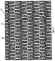
- FIG 4is an image taken of a backlight unit (25).
- a number of side-emitting LEDs (26), (not all labelled)are shown arranged in rows.
- the LEDsmay also be provided in columns (i.e. by rotating through 90°).
- the side-emitting LEDsemit light (27) into the plane of the backlight and substantially parallel with the base substrate.
- an LEDemits light in substantially the opposite direction to its immediate neighbours in a given row of LEDs.
- the backlightmay comprise, consist of, or consist essentially of such an arrangement of light sources.
- the LEDsmay be positioned so that they are substantially in a straight line.
- the LEDsmay be positioned so that alternate LEDs are in a straight line, thus forming two substantially parallel lines of LEDs in a given row or column.
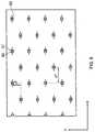
- Figure 5illustrates a preferred arrangement of LEDs in accordance with the present invention.
- a number of side-emitting LEDs (30), (not all labelled)are shown arranged in rows and columns and forming a repeating diamond like arrangement or array of LEDs across the backlight.
- the LEDsare arranged such that the light (31) is emitted in the same or substantially the same direction, i.e. into the plane of the backlight and substantially parallel with the base substrate, for all or substantially all of the LEDs.
- the x and y coordinatesare shown.
- the distance between the centre point of LEDs in a given row (x axis)may be about 24mm.
- the distance between the centre point of LEDs in a given column (y axis)may be about 24mm.
- the x axis displacement in adjacent rowsmay be about 12mm (this is indicated by x I ).
- the distance between adjacent rows of LEDsmay be about 12mm (this is indicated by y').
- This arrangementis particularly advantageous for a number of reasons. For example, this includes the provision of particularly good luminance uniformity which may also be achieved at a thickness of about 10mm or less for the full backlight. Other advantages include: effective spreading of thermal load; the presence of a back-plate is not evident visually; preferred spacing distribution for minimising path length in the light guide (i.e. optical loss is minimised); ease of electrical wiring.
- Figure 6illustrates a further arrangement of LEDs in accordance with the present invention.
- a number of side-emitting LEDs (40), (not all labelled)are shown arranged in rows and columns and forming a repeating off-set diamond like arrangement or array of LEDs across the backlight.
- the LEDsare arranged such that the light (41) is emitted into the plane of the backlight and substantially parallel with the base substrate, for all or substantially all of the LEDs.
- the lightis directed in opposite or substantially opposite directions in alternating rows.
- the x and y coordinatesare shown.
- the distance between the centre point of LEDs in a given row (x axis)may be about 24mm.
- the distance between the centre point of LEDs in a given columnmay be about 24mm.
- the x axis displacement in adjacent rowsmay be about 10.5mm (this is indicated by x II ) and about 13.5mm (this is indicated by x III ).
- the distance between adjacent rows of LEDsmay be about 12mm (this is indicated by y"). This spatial relationship may be repeated over the entirety, or substantially over the entirety, of the backlight.
- Figure 7illustrates a further arrangement of LEDs in accordance with the present invention.
- a number of pairs of side-emitting LEDs (50, 51), (not all labelled)are shown arranged in rows and columns and forming a repeating arrangement or array of LEDs across the backlight.
- the LEDsare arranged such that the light (52) is emitted into the plane of the backlight and substantially parallel with the base substrate, for all or substantially all of the LEDs.
- the lightis directed in opposite or substantially opposite directions for LEDs in each pair.
- the x and y coordinatesare shown.
- the distance between the centre of adjacent pairs of LEDs in a given row (x axis)may be about 48mm.
- the distance between the centre point of LEDs in a given columnmay be about 24mm.
- the x axis displacement of pairs of LEDs in adjacent rowsmay be about 12mm (this is indicated by x IV ) and 36mm (this is indicated by x V ).
- the distance between adjacent rows of LEDsmay be about 12mm (this is indicated by y III ). This spatial relationship may be repeated over the entirety, or substantially over the entirety, of the backlight.
- Figure 8illustrates a further arrangement of LEDs in accordance with the present invention.
- a number of pairs of side-emitting LEDs(60, 61), (not all labelled) are shown arranged in rows and columns and forming a repeating arrangement or array of LEDs across the backlight. The arrangement is similar to that shown in Figure 7 . However, the pairs of LEDs are arranged in a more regular diamond-like repeating pattern.
- the LEDsare arranged such that the light (62) is emitted into the plane of the backlight and substantially parallel with the base substrate, for all or substantially all of the LEDs. The light is directed in opposite or substantially opposite directions for LEDs in each pair.
- the x and y coordinatesare shown.
- the longest distance between pairs of LEDs in a given rowmay be about 48mm.
- the distance between LEDs in a given column (y axis)may be about 24mm.
- the x axis displacement of pairs of LEDs in adjacent rowsmay be about 24mm (this is indicated by x VI ).
- the distance between adjacent rows of LEDsmay be about 12mm (this is indicated by y IV ). This spatial relationship may be repeated over the entirety, or substantially over the entirety, of the backlight.
- a device in accordance with the inventionwas constructed as follows.
- a 0.125mm thick sheet of transparent polyesterwas used as a base substrate.
- a scattering structurecomprising white lines of ink was printed onto the underside of the polyester film.
- the ink usedwas a white acrylic based, UV curing polymer screen printable ink which is commercially available.
- On the opposite (or top) side of the polyester filmwas printed conducting tracks (silver particle loaded conducting epoxy) and conducting adhesive in order to mount a number of LEDs (Stanley Tw11451s-tr) onto the substrate and provide suitable electrical connections onto the conducting ink tracks.
- a cavity, about 0.7mm deepwas formed around the perimeter of the base substrate using a cavity layer structure.
- the cavitywas then filled with UV curing transparent polymer (Dymax 4-20688), thus forming a first light guide layer.
- a spacing elementwas positioned and secured on the first light guide layer and the diffuser (Shin Wha 97% haze film) was positioned on the spacing element.
- the distance of the diffuser to the light guide layerwas 9mm.
- the LEDswere concealed from observation from above, by the combination of light not coupled into the light guide layer and the diffuser.
- a thin aluminium heat sinking plate of 2mm thicknesswas fixed to the base substrate via discrete localised sections of thermal bonding material. Good uniformity of light was observed from the extracted light.
Landscapes
- Physics & Mathematics (AREA)
- General Physics & Mathematics (AREA)
- Optics & Photonics (AREA)
- Engineering & Computer Science (AREA)
- Microelectronics & Electronic Packaging (AREA)
- Planar Illumination Modules (AREA)
Description
- This invention relates to light guide devices and methods of manufacture. The light guide devices are suitable for use in a range of applications, particularly in connection with the backlighting of displays, for example, liquid crystal displays.
- A number of light guiding devices are known, see for example International patent publication numbers
WO 2007/138294 andWO2008/087572 and German Utility patent numberDE 20 2007 017224 . These devices are employed for a range of functions including illumination, backlighting, signage and display purposes. Typically, the devices are constructed from an injection moulded or machined transparent plastic component, where a light source, such as a fluorescent lamp or a plurality of light emitting diodes (LEDs), is integrated by means of mechanical attachment at the edge of the transparent plastic component. - Common to all of these devices is the fact that light from the light source is guided through a transparent guide, typically made of plastic, by total internal reflection. For backlighting applications, light is emitted in a substantially perpendicular direction to that of the direction of propagation of the light within the transparent guide. This is achieved through the light being directed so as to interact with scattering structures or films located within, or on the surface of, the transparent guide.
- The integration of fluorescent lamps or LEDs to the edge of the transparent light guide is not a straightforward process and thus significantly increases the complexity of the production process for these devices. Achieving a good coupling of the light source and the light guide is essential to the optical performance of the device. In addition, edge coupling of the light sources renders these components susceptible to mechanical damage during both the production process and the normal use of the device.
- In seeking to provide thin direct lit backlights, it is preferable to have light emitted into the plane of the light guide. Further benefit may be obtained if the light sources are distributed across the panel, so minimising the length of guiding in the light guide. This has the benefit of creating a thin and efficient backlight but has the disadvantage of compromising the light uniformity. For example, this may be through the creation of dark spots and/or more intense areas of light above or in the vicinity of the light source. Preferably, these dark spots and/or more intense areas of light should not be visible or, at least, reduced in appearance in order to provide at least acceptable, and more preferably, improved light uniformity. Existing solutions to this problem tend to add considerable thickness to the backlight.
- Many backlights fall into the categories of "edge-lit" or "direct-lit". These categories differ in the placement of the light sources relative to the output of the backlight, where the output area defines the viewable area of the display device. In edge-lit backlights, one or more light sources are disposed along an outer border or edge of the backlight construction outside the zone corresponding to the output area. The light sources typically emit light into a light guide, which has length and width dimensions of the order of the output area and from which light is extracted to illuminate the output area. In direct-lit backlights, an array of light sources is disposed directly behind the output area, and a diffuser is placed in front of the light sources to provide a more uniform light output. Some direct-lit backlights also incorporate an edge-mounted light, and are thus illuminated with a combination of direct-lit and edge-lit illumination.
- Apart from producing light, the light sources also produce heat. If the heat dissipates into a liquid crystal panel for example, the display quality may be adversely affected. Because the transfer of heat to the liquid crystal panel is unlikely to be uniform, the liquid crystal layer within the liquid crystal panel may be subjected to different degrees of heating. This non-uniform distribution of heat may also affect the switching of thin film transistors inside the liquid crystal display and the overall display quality of the liquid crystal panel may deteriorate. There are numerous challenges to overcome in thermally managing a backlight unit for use in combination with displays. Addressing issues surrounding thermal management should not result in an unacceptable increase in weight or thickness or compromise the mechanical integrity of the backlight unit. In addition, the optical performance of the backlight unit should not be significantly compromised.
- Other challenges facing display manufacturers, such as those incorporating large area LED Back Light Units (BLUs) include producing a thin and efficient device which enables 2-d or 3-d spatial dimming to support high display performance and reduced power consumption. This has proved problematic for both edge-lit and direct lit devices and has typically resulted in thicker backlight devices. 2-d dimming relates to when the image content of the display is achieved by only switching on selected areas of the backlight which match or correspond to the desired image thus resulting in significant power reduction. 3-d dimming further incorporates the use of colour.
- The beam angle of light emerging from a backlight and the uniformity of said beam angle are important in determining the efficiency and the viewing angle of the display that is being illuminated. Some degree of control over the range of light output angles provided by the backlight is desirable.
- It is an object of the present invention to provide a light guiding device that addresses one or more of the aforesaid issues. In particular, it is an object of the present invention to provide a light guiding device that addresses the problems associated with thermal management.
- In a first aspect of the present invention, there is provided a light guide device comprising a base substrate having a first refractive index, upon a first surface of which are mounted one or more light sources and a first guide layer having a second refractive index that is optionally less than or equal to the first refractive index and which comprises a light output surface, the first guide layer being arranged so as to encapsulate the one or more light sources upon the first surface, wherein the base substrate and the guide layer form a composite structure for guiding light produced by the one or more light sources over the first surface, further comprising thermal bonding material in contact with the lower surface of the base substrate wherein the lower surface is opposite and parallel or substantially parallel to the first surface, and wherein said thermal bonding material contacts a heat sink plate and forms an air gap between the lower surface of the base substrate and the heat sink plate. The thermal bonding material is present in discrete portions and is positioned in line or substantially in line with the one or more sources of light. The non-continuous nature of the thermal bonding material means that an air gap or gaps are formed between the substrate and the heat sink plate thus facilitating efficient heat dissipation. Advantageously, the heat sink plate and the base substrate are not optically coupled.
- Advantageously, said one or more light sources are positioned directly behind the light output surface and direct light parallel to the plane of the base substrate.
- The lower surface of the base substrate may be referred to herein as a second surface of the base substrate. As such, the second (or lower) surface is opposite the first surface of the base substrate.
- The light guide device may further comprise one or more features or structures that break or disrupt the total internal reflection of guided light. For example, the light guide device may comprise one or more scattering and/or reflective and/or refractive structures arranged so as to direct light away from the first surface and in the direction of the light output surface. For example, the one or more scattering and/or reflective and/or refractive structures may be located at the interface between the base substrate and the first light guide layer and/or on the lower surface of the substrate which is opposite the first surface.
- The light guide device may comprise a diffuser located above the light output surface.
- Upon the first guide layer there may be mounted a second guide layer having a third refractive index that is equal to or greater than the refractive index of the first guide layer and at the interface between the first and second guide layer and above the one or more sources of light may be located one or more light scattering and/or reflective and/or refractive structures. The concealment of the one or more light sources may be provided by only, or substantially only, light directed normal, or substantially normal, to the plane of the substrate in combination with the diffuser and optionally in combination with a single light guide layer.
- The one or more light sources may direct at least some light parallel to the plane of the base substrate. Advantageously, the one or more light sources comprise, or consist of, or consist essentially of side emitting LEDs. Preferably, the one or more light sources form an array of side-emitting LEDs across the base substrate in a direct-lit arrangement. Preferably, a portion of the light emitted by the one or more light sources is not coupled into the light guide but is directed normal or substantially normal to the base substrate and in the direction of the light output surface. Typically, this is less than about 20% of the light emitted from the one or more light sources, for example less than about 10% of the light emitted from the one or more light sources, for example about 2% or less of the light emitted from the one or more light sources. The one or more light sources may also include a number of top emitting LEDs. The top emitting LEDs emit light substantially perpendicularly to the main light output of the side emitting LEDs and in the direction of the light output surface. The array of side emitting LEDs may form a two dimensional array of side emitting LEDs in a direct-lit arrangement. The array may comprise, consist of, or consist essentially of a number of rows and/or columns of LEDs which may vary in which direction they direct at least some light parallel to the plane of the base substrate. For example, the LEDs may be arranged so that for an LED in a particular column or row the LED may direct light in substantially the opposite direction when compared with either of the two LEDs to which it is immediately adjacent in said column or row. For example, for two adjacent LEDs, the angle between the direction of light generated by the first LED in a first direction which is substantially parallel to the plane of the base substrate and the direction of light generated by the second LED in a second direction which is also substantially parallel to the plane of the base substrate may be about 180°. In a given row or column, the LEDs may be positioned so that they are substantially in a straight line. The LEDs may be positioned so that alternate LEDs are in a straight line thus forming two substantially parallel lines of LEDs in a given row or column. In an alternative arrangement, the LEDs may be positioned forming a repeating diamond like arrangement or array of LEDs across the substrate. The LEDs may be arranged such that the light is emitted in the same or substantially the same direction for all or substantially all of the LEDs.
- According to a second aspect of the present invention, there is provided a method of producing a light guide device, the method comprising:
- i. mounting one or more light sources onto a first surface of a base substrate having a first refractive index; and
- ii. adding a first guide layer, having a second refractive index that may be less than or equal to the first refractive index, to the first surface so as to encapsulate the one or more light sources upon the first surface;
- iii. applying one or more scattering and/or reflective and/or refractive structures on the first guide layer and/or the substrate before the substrate and the first guide layer are combined, such that said one or more scattering and/or reflective and/or refractive structures are located at the interface between the substrate and the first guide layer; or applying one or more scattering and/or reflective and/or refractive structures on the lower surface of the base substrate;
- iv. adding a heat sink plate to the lower surface of the base substrate which is opposite the first surface of the base substrate, wherein the heat sink plate is in contact with said base substrate via discrete portions of thermal bonding material positioned in line with the one or more light sources.
- In the method according to the second aspect of the invention, further steps may be incorporated in order to mount a second guide layer having a third refractive index that is equal to or greater than the refractive index of the first guide layer and at the interface between the first and second guide layer and above the one or more sources of light may be located one or more light scattering and/or reflective and/or refractive structures.
- The method according to the second aspect of the invention provides a means for guiding light produced by the one or more light sources over the first surface of the base substrate. The light may be guided within the composite structure by total internal reflection.
- Preferably, the method of adding the first guide layer to the first surface of the base substrate and/or mounting the second guide layer onto the first guide layer comprises:
- i. applying a liquid polymer on the first surface of the base substrate and/or first guide layer; and
- ii. curing the liquid polymer on the first surface of the base substrate and/or first guide layer.
- The method of applying the liquid polymer on the first surface of the base substrate and/or the first guide layer may comprise printing, stencilling or dispensing the liquid polymer.
- The step of applying one or more scattering and/or reflecting and/or refracting structures so as to redirect light away from the first surface of the base substrate or the first guide layer may comprise printing a patterned, reflecting ink layer.
- The arrangement of the guide layer or layers in relation to the light sources provides a light guiding device that exhibits enhanced mechanical protection for the light sources. Furthermore, a device is provided that is simple to produce and which exhibits enhanced optical coupling of the light within the device. For those embodiments where the refractive index of the base substrate and the optional second guide layer are selected to be equal to or higher than that of the first guide layer, the generated light is guided within both the light transmissive or transparent base substrate and the guide layer or layers due to the effects of total internal reflection.
- The base substrate and the first and second guide layers may be light transmissive and preferably transparent to the light generated by the one or more light sources. The terms "transparent" and "transmissive" relate to the optical properties of particular components of the device relative to the wavelength of the light generated by the incorporated light sources.
- According to a third aspect of the present invention, there is provided a display device comprising a light guiding device according to the various aspects including the first aspect of the invention. The display device may be a liquid crystal display device and may therefore comprise a liquid crystal cell which may also be referred to as a liquid crystal panel.
- The present invention seeks to provide one or more of the following advantages: a more uniform light guide device (including uniform or substantially uniform luminance) with reduced/no dark spots when viewed in use; efficient light distribution resulting in lower power requirements; a thinner, lighter structure; a device comprising a reduced number of system components. The devices according to the present invention may advantageously be used for 2-d and 3-d dimming. In particular, the present invention seeks to provide effective thermal management of backlight devices without adversely affecting the optical performance.
- The present invention also provides improved optical coupling from the light sources to the light guide, short average optical path lengths resulting in minimal optical loss in the light guide, minimal surface scattering and beneficial extracted light beam profiles. For example the present invention can provide good uniformity of extracted light possessing desirable angles of distribution, e.g. about +/- 30° from the normal at full width half maximum. In addition, these features serve to provide a highly optically efficient (for example equal to or greater than about 90%) backlight which is scalable up to >80inches (diagonal).
- The base substrate may be light transmissive and may be transparent. The base substrate may be formed from a transparent polymer sheet such as polyester or polycarbonate. The thickness of the transparent base substrate is typically of the order of about 0.1 mm, for example in the range of about 0.1 mm to about 0.2mm. The refractive index of the base substrate is typically equal to or greater than 1.5. For example, the refractive index of the base substrate may be 1.50 to 1.58.
- The base substrate may be a microstructured film which has an ink in contact with one or more of said microstructures, wherein said ink reduces the amount of light escaping from said microstructure. Alternatively, a microstructured film may be applied to the base substrate. Brightness Enhancement Films (BEFs) are suitable microstructured films for use in the present invention. A suitable example of a microstructured film is BEF III Brightness Enhancement Film, which is commercially available from 3M. A particular film from this range is made from polyester substrate of thickness 127 microns and possesses a prism structure, varying in one direction, in acrylic polymer. The prism structure is 28 microns high, has a pitch of 50 microns and the prism angle is 90º. Such a film, suitably modified with ink, may be used in the present invention to produce a backlight with a non-symmetrical beam angle of the scattered light, provided that light is input from one of the edges parallel to the prism direction. The ink which may be applied to the microstructures may be light transmissive. Light transmissive ink has the effect of planarising or flattening the microstructures and facilitates light guiding by total internal reflection over the film layer. Light transmissive or transparent ink reduces the amount of light escaping from the film at the microstructure on which it is deposited. Without wishing to be bound by theory, it is believed that light which is being guided by total internal reflection through the light guide plate, encounters a substantially flat surface at the interface between the planarised film layer and air. The substantially flat, planarised surface will retain the total internal reflection and the light will continue to be guided within the light guide device. The structured surface which is not modified with an ink scatters light out from the light guide device by breaking the total internal reflection. Reflective ink may also be used on the microstructures as an alternative means for facilitating extraction of light out from the light guide device and controlling the direction in which the light is extracted. Suitable reflective inks for use in the present invention may comprise metal loaded polymers. Preferably, the refractive indices of the ink and the microstructure should match as closely as possible. For example, the difference in refractive indices should be about 2% or less, more preferably about 1% or less.
- The ink, which is typically a polymeric material, may be applied to the microstructured surface of the film to form a thin pattern of features according to any of a number of methods and may be referred to in general terms as an additive printing process. For example, conventional screen printing, incorporates the use of a mesh screen with openings corresponding to the pattern required to be printed. This pattern facilitates the accurate delivery of a volume of ink to the required areas of the microstructures to be planarised. A suitable UV curing ink is Windowtex Gloss which is an acrylic based, transparent UV curing polymer screen printable ink and is commercially available from MacDermid Autotype. Suitable inks for use in the present invention include those which may be UV or solvent cured. Other suitable examples of additive printing methods include stencil printing, ink jet printing, flexographic printing and other known lithographic techniques.
- The ink may be applied in varying amounts and shapes. This may depend on how close to the light source the ink is being deposited. The intensity of the light becomes less as the distance from the light source increases. To take account of this, larger sized light transmissive ink dots which are more closely spaced may be deposited closer to the position of the light source resulting in small areas of unplanarised microstructure, whereas smaller sized light transmissive ink dots which are more widely spaced may be deposited as the distance from the light source increases, resulting in larger areas of unplanarised microstructure.
- The light source can be any of those known to those skilled in the art, including those which are suitable for use in backlighting. Such light sources include one or more LEDs. The light may be non-directional. The LEDs can be any of the designs known to those skilled in the art, including edge-emitting, side emitting, top emitting or bare die LEDs. The LEDs may be selected from one or more of a range of colours. For example, the LEDs may be white. White light may also be generated by combining red, green and blue LEDs. Typically, an LED suitable for use in the present invention is of the order of about 1 mm in each dimension.
- The light sources may be arranged to direct substantially all of the light into the light guide. Advantageously, they are selected from side-emitting LEDs wherein the light is directed parallel, or substantially parallel to the plane of the substrate. Even more advantageously a proportion of the light is not coupled into the light guide but is allowed to propagate in the direction of the output surface. For example, less than about 20% of the light emitted from the one or more light sources, for example less than about 10% of the light emitted from the one or more light sources, for example about 2% or less of the light is allowed to propagate in such a manner. The effect of allowing this light to propagate towards the output surface is that the appearance of the light sources is concealed when viewed in normal use and the light is distributed more uniformly. In particular, this light allows a diffuser to be positioned more closely to the light guide layer than in other conventional backlights.
- Advantageously, the one or more lights sources are arranged to provide direct-lit light guide devices, including direct-lit backlight units. The one or more light sources may form an array of light sources across the base substrate in a direct-lit arrangement. This arrangement serves to provide a good thermal solution compared to more conventional arrangements. This direct-lit arrangement may consist of an array of light sources forming a series of rows and columns across the whole of, or substantially the whole of, the base substrate. The array may comprise, consist of or consist essentially of an array of side-emitting LEDs in a direct-lit arrangement. Such an array may also include a number of top emitting LEDs. The one or more light sources may be arranged in a regular repeating pattern across the base substrate.
- Electrical tracks may be patterned onto the base substrate which may be transparent, so forming electrical bonding pads for the one or more light sources and electrical connections for external electrical driving equipment. The electrical tracks may be patterned by etching methods, for example, using copper or gold, or by additive screen printing methods, for example, using silver loaded adhesive.
- The LED light sources may be electrically and mechanically attached to the electrical bonding pads by soldering or conducting adhesive methods.
- The guide layer or layers (which may also be referred to as light guide layers) which are typically suitable for use in a backlight unit may be transparent. The guide layer or layers may comprise a transparent flexible plastic polymer layer, typically of about 1 mm in thickness. The refractive index of the guide layer may have a refractive index of about 1.46 to 1.56.
- The refractive indices of the first and second guide layers may be substantially the same or the refractive index of the second guide layer may be higher than the first guide layer. For the situation where the second light guide layer has a higher refractive index, the difference in refractive indices may be as high as about 10%.
- The guide layers may be made from a range of available polymers, including acrylics, urethanes or polycarbonates.
- The guide layers may be combined using a standard lamination technique. Such a technique may require the use of a transparent adhesive which has a refractive index which is higher than both the first and second guide layers. The guide layers may be optically joined during manufacture. The method of combining the layers may comprise applying and curing a liquid polymer layer. Methods of curing may make use of one or more techniques including UV, thermal or two-part curing. The method may comprise printing, stencilling or dispensing the liquid polymer. Optically joined indicates the layers are combined in such a way that, optically, these layers are effectively indistinguishable. This technique may also be used for combining the first guide layer and the base substrate.
- Upon the first guide layer, which may be transparent, there may be mounted a second guide layer having a third refractive index that is equal to or greater than the refractive index of the first guide layer and at the interface between the first and second guide layer and above the one or more sources of light may be located one or more light scattering and/or reflective structures. The first and second light guide layers may be laminated together. Lamination may be achieved using a uv curable clear polymer adhesive such as Dymax.
- The light guide device may further comprise one or more features that break the total internal reflection of the guided light. For example, the light guide device may further comprise the light scattering and/or reflective and/or refractive structures which disturb the total internal reflection of the guided light. The application of the structures may be accomplished using standard printing, micromoulding, microstamping and microembossing techniques. Suitable scattering structures may be in the form of a patterned reflecting ink layer. Suitable scattering features include highly reflective white printed ink dots. In such an arrangement, each dot disturbs the total internal reflection of the guided light and causes the light to be scattered randomly and to escape from the light guide. The size and/or pitch of the dots may be varied to ensure uniform light scatter.
- The ink, which may be a polymeric material, may be applied to the base substrate or a guide layer to form a thin pattern of features, according to any of a number of methods and may be referred to in general terms as an additive printing process. For example, conventional screen printing incorporates the use of a mesh screen with openings corresponding to the pattern required to be printed. This pattern facilitates the accurate delivery of a volume of ink to the required areas of the guide layer or base substrate. Suitable inks for use in the present invention include those which may be UV or solvent cured. Other suitable examples of additive printing methods include stencil printing, ink jet printing, flexographic printing and other known lithographic techniques. The ink may be applied in varying amounts and shapes.
- Other suitable structures include microstructured surfaces which comprise a plurality of three dimensional features, or irregularities, which are proud of the surface and arranged on a scale of about 1 to about 1000 microns, independently, in width, depth and pitch, preferably about 5 to about 50 microns, more preferably about 20 to about 50 microns. Specific types of microstructures, or features, which are suitable for use in the present invention include prisms, pyramids, (micro)lenses, e.g. cylindrical or circular shaped lenses and random diffusing structures.
- Prism based microstructures may have a saw tooth shape structure varying in one direction across the entirety of the surface with a pitch of about 50 microns, wherein the pitch is the distance between the centre of adjacent microstructures. (Micro)lenses have a regular or random distribution of lenses, which may be of a low focal length, distributed across the surface on a scale of about 10 to 20 microns. The diffusing structures may possess a random surface texture which is also on a scale (depth and pitch) of about 10 to 100 microns.
- The light scattering and/or reflective and/or refractive features may also be referred to as light extraction features.
- The heat sink plate may be located behind and substantially parallel to the base substrate, which may be transparent, and may be connected to the substrate via discrete portions of thermal bonding material. The thermal bonding material may advantageously be located in line or substantially in line with the one or more light sources. The positioning of the discrete portions of thermal bonding material means that there is an air gap located between the substrate and the heat sink plate and between the discrete portions of thermal bonding material. The air gap means that the heat sink plate does not interfere with the light guiding mechanism and ensures uniform light scattering from the features that break the total internal reflection of the guided light, e.g. scattering features. Advantageously, the base substrate and the heat sink plate are not optically coupled. A backlight reflector element, e.g. film may be located in the vicinity of the air gap or gaps to improve optical efficiency. For example, the backlight reflector film may be located on the lower surface of the substrate and/or on the upper surface of the heat sink plate.
- The heat sink plate may be made from materials which assist in the dissipation of the heat. Suitable examples include metals such as aluminium. The heat sink plate is typically about 0.2mm to 10mm in thickness, for example about 2mm in thickness or less. The thermal bonding material may be an adhesive such as an epoxy or a silicone or it may be a pressure sensitive adhesive tape or screen/stencil printable polymer with high thermal conductivity. The adhesive may be applied using a needle or by using screen printing. The adhesive tape may be applied using a standard taping machine. The heat sink plate may be a regular piece of solid flat material and which does not comprise any gaps or slots. Alternatively, the heat sink plate may comprise a number of slots or gaps, optionally of varying size. The gaps or slots may be introduced by machining or manufacturing said gaps or slots into a heat sink plate. A number of cooling fins may be formed by the presence of the gaps or slots. The cooling fins may thus be formed in the plane of the substrate providing a thin arrangement and may be suitably aligned with the one or more light sources. The presence of cooling fins typically results in a more effective and lighter heat sink arrangement.
- The use of the heat sink plate according to the present invention provides the means for operating at higher current at a wider temperature range. By running at higher current the light output can be increased thus reducing the number of light sources e.g. LEDs.
- The substrate and heat sink may be combined using lamination techniques.
- The diffuser may be positioned more closely to the light guide layer when compared with more conventional light guide devices. For example, the distance from the top of the light guide layer to the bottom of the diffuser may be less than about 12mm. For example the distance may be as low as about 9mm or about 2mm. Typically, the distance between the light guide layer and the diffuser is greater than about 2mm.
- The diffuser may be kept separate from the light guide layer by means of a conventional spacing arrangement. For example, a spacing element is located around the edge of the light guide layer.
- The diffuser may be chosen from conventional diffusers used in backlights.
- The light guide devices according to the present invention may be employed for a range of functions including illumination, backlighting, signage and display purposes. Liquid crystal devices are well known in the art. A liquid crystal display device operating in a transmissive mode typically comprises a liquid crystal cell, which may also be referred to as a liquid crystal panel, a backlight unit which may incorporate a light guide device, and one or more polarisers. Liquid crystal cells are also well known devices. In general, liquid crystal cells typically comprise two transparent substrates between which is disposed a layer of liquid crystal material. A liquid crystal display cell may comprise two transparent plates which may be coated on their internal faces respectively with transparent conducting electrodes. An alignment layer may be introduced onto the internal faces of the cell in order that the molecules making up the liquid crystalline material line up in a preferred direction. The transparent plates are separated by a spacer to a suitable distance, for example about 2 microns. The liquid crystal material is introduced between the transparent plates by filling the space in between them by flow filling. Polarisers may be arranged in front of and behind the cell. The backlight unit may be positioned behind the liquid crystal cell using conventional means. In operation, a liquid crystal cell, operating in a transmissive mode, modulates the light from a light source such as a backlight unit which may comprise a light guide device.
- Embodiments of the invention will now be described, by way of example only and without limitation, with reference to the accompanying drawings and the following Examples, in which:
Figure 1 illustrates a light guide device according to the present invention;Figure 2 illustrates a light guide device according to the present invention;Figures 3a and 3b illustrate a plan view of a heat sink plate comprising a number of slots and their position relative to light sources and a light guide device comprising such a heat sink plate respectively, both in accordance with the present invention;Figure 4 is an image of a backlight according to the present invention;Figures 5 to 8 illustrate particular arrangements of the light sources according to the present invention.- In
Figure 1 , a light guide device (1) in side elevation comprises a transparent base substrate (2) made from a transparent polymer sheet such as polyester or polycarbonate and having a refractive index n2. On top of the transparent base substrate (2) are bonded a number of light sources (3) in the form of LEDs. Electrical bonds are indicated at (3a). The distance between the LEDs is typically about 10mm to about 200mm. The LEDs illustrated in this particular embodiment are side emitting LEDs and the direction of the light emitted from the LEDs is indicated at (5) and is directed parallel to the plane of the substrate. In an alternative embodiment there may also be present a number of top emitting LEDs. Covering the LEDs and the remaining area of the top surface of the transparent base substrate (2) is a first transparent guide layer (4) also formed from a plastic polymer and having a refractive index n4. Located on the lower surface of the transparent base substrate is a scattering structure (6) in the form of a patterned reflecting ink layer. - Optionally (not shown), and located on the upper surface of the first transparent guide layer may be a second transparent guide layer having a refractive index n6.
- At the perimeter interface between the transparent base substrate (2) and the first transparent guide layer (4), a cavity layer structure (not shown) may be incorporated in order to form a suitable cavity in which the LEDs (3) may be embedded.
- The refractive indices of the transparent base substrate and the first transparent guide layer may be such that they satisfy the inequality n2 ≥ n4.
- When present, the refractive indices of the second transparent guide layer and the first transparent guide layer may be such that they satisfy the inequality n6 ≥ n4.
- In the embodiment shown, light, generated by the LED light sources is initially coupled into the transparent guide layer so as to propagate in a direction substantially parallel to a plane defined by the transparent base substrate. The generated light is guided within both the transparent base substrate and the transparent guide layer or layers due to the effects of total internal reflection. Therefore, the transparent base substrate and the transparent guide layer or layers form a composite structure that acts as the guiding media for the light generated by the encapsulated LED light sources (3).
- When the light has propagated as far as the scattering structure (6), it interacts with this structure so as to be redirected and so exit (7) the device via the top surface of the transparent guide layer so providing a backlighting function.
- The scattering and/or reflective and/or refracting structures (6) may comprise highly reflective white ink dots. Both the dot size and/or pitch may be varied in order to fine tune the scattering effects.
- A heat sink plate (8) is contacted to the lower surface of the base substrate (2) via discrete portions of thermal bonding material (9). An air gap (10) is formed through the use of discrete portions of thermal bonding material. A further light reflecting structure (11) may optionally be introduced on either the lower surface of the substrate (2) or on the upper surface of the heat sink plate (8).
- As a result of the fact that there is no air gap between the output of the light sources and the light guiding media, the transparent guide layers provide a simpler, and enhanced means of optically coupling the light within the device.
Figure 2 illustrates a light guide device essentially as shown inFigure 1 but with an additional transparent guide layer (15) having a refractive index n6 present on the surface of the first transparent guide layer (4). Located at the interface between the first and second transparent guide layers are scattering and/or reflecting and/or refracting structures (16). The refractive indices of the second transparent guide layer and the first transparent guide layer are such that they satisfy the inequality n6≥n4. As a result and can be seen inFigure 2 , light indicated by 5a and 5b generated by the LED light source is initially coupled into the transparent guide layers so as to propagate in a direction substantially parallel to a plane defined by the transparent base substrate. With the refractive index of the transparent base substrate and the second transparent guide layer selected to be equal or higher than that of the first transparent guide layer, the generated light is guided within both the transparent base substrate and the transparent guide layers due to the effects of total internal reflection. Therefore, the transparent base substrate and the transparent guide layers form a composite structure that acts as the guiding media for the light generated by the encapsulated light sources. When the light (5a, 5b) has propagated as far as the scattering structure (6a), it interacts with this structure so as to be redirected and so exit the device via the top surface of the transparent guide layer, either directly, indicated at (7a) or via the scattering and/or reflecting and/or refracting structure, indicated at (7b), so providing a backlighting function. The structure (16) is located at the interface between the first and second transparent guide layers and over the LEDs such that the scattering effects of the structure (16) and the structure (6a) reduce or remove completely the dark appearance of the top surface, indicated at (17) of the LEDs. The second or upper guide layer (15) is providing uniform light distribution across the complete area. In use and when incorporated into a suitable device such as a liquid crystal display, the light guide device illustrated is viewed substantially in the direction indicated at (18). The scattering structures (6a) and (16) may comprise highly reflective white ink dots. Both the dot size and/or pitch may be varied in order to fine tune the scattering effects.Figures 3a and 3b relate to a heat sink plate for use in accordance with the present invention incorporating a number of slots or gaps. More specifically,Figure 3a illustrates the arrangement of slots relative to the positioning of light sources e.g. LEDs andFigure 3b is a side view of a light guide device incorporating the slotted heat sink plate. InFigure 3a , a number of slots (30) are shown positioned relative to the LED light sources (3) which are arranged in a repeating diamond-like arrangement. The cooling fins (not shown) are in line or substantially in line with the LED light sources. InFigure 3b , a side view of a light guide device incorporating the slotted heat sink plate is illustrated. The position of the slots (30) is indicated in the heat sink plate (8).Figure 4 is an image taken of a backlight unit (25). A number of side-emitting LEDs (26), (not all labelled) are shown arranged in rows. The LEDs may also be provided in columns (i.e. by rotating through 90°). The side-emitting LEDs emit light (27) into the plane of the backlight and substantially parallel with the base substrate. In this particular embodiment, an LED emits light in substantially the opposite direction to its immediate neighbours in a given row of LEDs. The backlight may comprise, consist of, or consist essentially of such an arrangement of light sources. In a given row or column, the LEDs may be positioned so that they are substantially in a straight line. For example, as shown inFigure 4 , the LEDs may be positioned so that alternate LEDs are in a straight line, thus forming two substantially parallel lines of LEDs in a given row or column.Figure 5 illustrates a preferred arrangement of LEDs in accordance with the present invention. A number of side-emitting LEDs (30), (not all labelled) are shown arranged in rows and columns and forming a repeating diamond like arrangement or array of LEDs across the backlight. The LEDs are arranged such that the light (31) is emitted in the same or substantially the same direction, i.e. into the plane of the backlight and substantially parallel with the base substrate, for all or substantially all of the LEDs. In the embodiment shown inFigure 5 , the x and y coordinates are shown. The distance between the centre point of LEDs in a given row (x axis) may be about 24mm. The distance between the centre point of LEDs in a given column (y axis) may be about 24mm. The x axis displacement in adjacent rows may be about 12mm (this is indicated by xI). The distance between adjacent rows of LEDs may be about 12mm (this is indicated by y'). This spatial relationship may be repeated over the entirety, or substantially over the entirety, of the backlight. This spatial relationship may be more generally described by xI = (or is substantially equal to) y'. This arrangement is particularly advantageous for a number of reasons. For example, this includes the provision of particularly good luminance uniformity which may also be achieved at a thickness of about 10mm or less for the full backlight. Other advantages include: effective spreading of thermal load; the presence of a back-plate is not evident visually; preferred spacing distribution for minimising path length in the light guide (i.e. optical loss is minimised); ease of electrical wiring.Figure 6 illustrates a further arrangement of LEDs in accordance with the present invention. A number of side-emitting LEDs (40), (not all labelled) are shown arranged in rows and columns and forming a repeating off-set diamond like arrangement or array of LEDs across the backlight. The LEDs are arranged such that the light (41) is emitted into the plane of the backlight and substantially parallel with the base substrate, for all or substantially all of the LEDs. The light is directed in opposite or substantially opposite directions in alternating rows. In the embodiment shown inFigure 6 , the x and y coordinates are shown. The distance between the centre point of LEDs in a given row (x axis) may be about 24mm. The distance between the centre point of LEDs in a given column (y axis) may be about 24mm. The x axis displacement in adjacent rows may be about 10.5mm (this is indicated by xII) and about 13.5mm (this is indicated by xIII). The distance between adjacent rows of LEDs may be about 12mm (this is indicated by y"). This spatial relationship may be repeated over the entirety, or substantially over the entirety, of the backlight.Figure 7 illustrates a further arrangement of LEDs in accordance with the present invention. A number of pairs of side-emitting LEDs (50, 51), (not all labelled) are shown arranged in rows and columns and forming a repeating arrangement or array of LEDs across the backlight. The LEDs are arranged such that the light (52) is emitted into the plane of the backlight and substantially parallel with the base substrate, for all or substantially all of the LEDs. The light is directed in opposite or substantially opposite directions for LEDs in each pair. In the embodiment shown inFigure 7 , the x and y coordinates are shown. The distance between the centre of adjacent pairs of LEDs in a given row (x axis) may be about 48mm. The distance between the centre point of LEDs in a given column (y axis) may be about 24mm. The x axis displacement of pairs of LEDs in adjacent rows may be about 12mm (this is indicated by xIV) and 36mm (this is indicated by xV). The distance between adjacent rows of LEDs may be about 12mm (this is indicated by yIII). This spatial relationship may be repeated over the entirety, or substantially over the entirety, of the backlight.Figure 8 illustrates a further arrangement of LEDs in accordance with the present invention. A number of pairs of side-emitting LEDs (60, 61), (not all labelled) are shown arranged in rows and columns and forming a repeating arrangement or array of LEDs across the backlight. The arrangement is similar to that shown inFigure 7 . However, the pairs of LEDs are arranged in a more regular diamond-like repeating pattern. The LEDs are arranged such that the light (62) is emitted into the plane of the backlight and substantially parallel with the base substrate, for all or substantially all of the LEDs. The light is directed in opposite or substantially opposite directions for LEDs in each pair. In the embodiment shown inFigure 8 , the x and y coordinates are shown. The longest distance between pairs of LEDs in a given row (x axis) may be about 48mm. The distance between LEDs in a given column (y axis) may be about 24mm. The x axis displacement of pairs of LEDs in adjacent rows may be about 24mm (this is indicated by xVI). The distance between adjacent rows of LEDs may be about 12mm (this is indicated by yIV). This spatial relationship may be repeated over the entirety, or substantially over the entirety, of the backlight.- A device in accordance with the invention was constructed as follows. A 0.125mm thick sheet of transparent polyester was used as a base substrate. A scattering structure comprising white lines of ink was printed onto the underside of the polyester film. The ink used was a white acrylic based, UV curing polymer screen printable ink which is commercially available. On the opposite (or top) side of the polyester film was printed conducting tracks (silver particle loaded conducting epoxy) and conducting adhesive in order to mount a number of LEDs (Stanley Tw11451s-tr) onto the substrate and provide suitable electrical connections onto the conducting ink tracks. A cavity, about 0.7mm deep was formed around the perimeter of the base substrate using a cavity layer structure. The cavity was then filled with UV curing transparent polymer (Dymax 4-20688), thus forming a first light guide layer. A spacing element was positioned and secured on the first light guide layer and the diffuser (Shin Wha 97% haze film) was positioned on the spacing element. The distance of the diffuser to the light guide layer was 9mm. The LEDs were concealed from observation from above, by the combination of light not coupled into the light guide layer and the diffuser. A thin aluminium heat sinking plate of 2mm thickness was fixed to the base substrate via discrete localised sections of thermal bonding material. Good uniformity of light was observed from the extracted light.
Claims (20)
- A light guide device (1) comprising a base substrate (2) having a first refractive index, upon a first surface of which are mounted one or more light sources (3) and a first guide layer (4) having a second refractive index that is less than or equal to the first refractive index and which comprises a light output surface, the first guide layer (4) being arranged so as to encapsulate the one or more light sources (3) upon the first surface, wherein the base substrate (2) and the guide layer (4) form a composite structure for guiding light (5) produced by the one or more light sources (3) over the first surface,
characterised in that
the light guide device (1) further comprises a heat sink plate (8) attached to the lower surface of the base substrate (2) via discrete portions of thermal bonding material (9) positioned in line with the one or more light sources (3) and there are one or more air gaps (10) formed between the heat sink plate (8) and the substrate (2). - A light guide device (1) according to claim 1, wherein said one or more light sources (3) are positioned directly behind the light output surface and direct light parallel to the plane of the base substrate (2).
- A light guide device (1) according to claims 1 or 2, wherein the light guide device (1) comprises one or more features that break the total internal reflection of guided light (6) so as to direct light away from the first surface of the base substrate (2) and in the direction of the light output surface and wherein the features that break the total internal reflection of guided light (6) comprise reflecting and/or scattering and/or refractive structures.
- A light guide device (1) according to claim 1, wherein the light guide device (1) comprises one or more reflecting light scattering structures arranged so as to direct light away from the first surface of the base substrate (2).
- A light guide device (1) according to any one of claims 1 to 4, wherein upon the first guide layer (4) is mounted a second guide layer (15) having a third refractive index that is equal to or greater than the first guide layer (4) and at the interface between the first (4) and second (15) guide layers and above the one or more sources of light (3) is located one or more light scattering and/or reflective and/or refractive structures (16).
- A light guide device (1) according to any one of claims 1 to 5, wherein the base substrate (2) and light guide layer (4) or layers (4, 15) are formed from light transparent polymers or wherein the base substrate (2) and/or light guide layer (4) or layers (4, 15) are formed from a flexible light transparent polymer or polymers.
- A light guide device (1) according to any one of claims 1 to 6, wherein the base substrate (2) is about 0.1 mm thick.
- A light guide device (1) according to any one of claims 1 to 7, wherein the light source (3) is selected from one or more LEDs and wherein the one or more LEDs may comprise, may consist essentially of, or may consist of side-emitting LEDs.
- A light guide device (1) according to the previous claim, wherein the one or more LEDs form an array of side-emitting LEDs across the base substrate in a direct-lit arrangement and optionally the array further comprises top emitting LEDs.
- A light guide device (1) according to any one of the previous claims, wherein the base substrate (2) is, or is in contact with, a microstructured film which has an ink in contact with one or more of said microstructures, wherein said ink reduces the amount of light escaping from said microstructure and wherein for example the microstructured film is a brightness enhancement film.
- A light guide device (1) according to claim 10, wherein the ink is a light transmissive ink.
- A light guide device (1) according to claim 11, wherein the light transmissive ink has the effect of planarising or flattening the microstructures and facilitates light guiding by total internal reflection over the film.
- A light guide device (1) according to any one of claims 1 to 12, wherein the one or more light sources (40, 41) are present in a direct lit arrangement in a two dimensional array forming a series of rows and/or columns of light sources, wherein in a given row and/or column for two adjacent light sources the angle between the direction of light generated by the first light source (40) in a first direction which is substantially parallel to the plane of the base substrate (2) and the direction of light generated by the second light source (41) in a second direction which is also substantially parallel to the plane of the base substrate (2) is about 180°.
- A light guide device (1) according to any one of claims 1 to 12, wherein the one or more light sources (60, 61) are positioned directly behind the light output surface in a direct lit arrangement forming a series of rows and/or columns comprising the light sources (60, 61) wherein in a given column and/or row a light source (60) directs light in substantially the opposite direction when compared with the light sources (61) to which it is immediately adjacent.
- A light guide device (1) according to any one of claims 1 to 12, wherein the one or more light sources (30) are positioned directly behind the light output surface in a direct lit arrangement forming a series of rows and/or columns comprising the light sources (30) wherein all or substantially all of the one or more light sources (30) are arranged to emit light in the same or substantially the same direction substantially parallel or parallel to the plane of the base substrate (2).
- A light guide device (1) according to any one of claims 1 to 15, wherein the one or more light sources (30) are arranged in a diamond-like repeating pattern and wherein optionally the one or more light sources (30) are spaced equally in rows and spaced equally in columns.
- A light guide device (1) according to any one of the previous claims wherein the light guide device (1) further comprises a diffuser above the light output surface.
- A light guide device (1) according to any one of the previous claims wherein the heat sink plate (8) comprises slots and cooling fins.
- A method of producing a light guide device (1), the method comprising:i. mounting one or more light sources (3) onto a first surface of a base substrate (2) having a first refractive index; andii. adding a first guide layer (4), having a second refractive index that may be less than or equal to the first refractive index, to the first surface so as to encapsulate the one or more light sources (3) upon the first surface;iii. applying one or more scattering and/or reflective and/or refractive structures (6) on the first guide layer (4) and/or the substrate (2) before the substrate (2) and the first guide layer (4) are combined, such that said one or more scattering and/or reflective and/or refractive structures (6) are located at the interface between the substrate (2) and the first guide layer (4); or applying one or more scattering and/or reflective and/or refractive structures (6) on the lower surface of the base substrate (2);iv. adding a heat sink plate (8) to the lower surface of the base substrate (2) which is opposite the first surface of the base substrate (2), wherein the heat sink plate (8) is in contact with said base substrate (2) via discrete portions of thermal bonding material (9) positioned in line with the one or more light sources (3).
- A display device, for example a liquid crystal display device, comprising the light guide device according to any one of claims 1 to 18.
Applications Claiming Priority (5)
| Application Number | Priority Date | Filing Date | Title |
|---|---|---|---|
| GB0903862AGB2468353A (en) | 2009-03-05 | 2009-03-05 | A light guide device |
| GB0905070AGB2468875A (en) | 2009-03-24 | 2009-03-24 | Light guide comprising rows and/or columns of LED's |
| GB0920333AGB2475511A (en) | 2009-11-20 | 2009-11-20 | Light guide with heat sink |
| GB0920922AGB2475738A (en) | 2009-11-30 | 2009-11-30 | Light guide with heat sink |
| PCT/GB2010/050388WO2010100505A1 (en) | 2009-03-05 | 2010-03-05 | Light guides |
Publications (2)
| Publication Number | Publication Date |
|---|---|
| EP2404202A1 EP2404202A1 (en) | 2012-01-11 |
| EP2404202B1true EP2404202B1 (en) | 2016-08-10 |
Family
ID=42136503
Family Applications (1)
| Application Number | Title | Priority Date | Filing Date |
|---|---|---|---|
| EP10707119.3AActiveEP2404202B1 (en) | 2009-03-05 | 2010-03-05 | Light guides |
Country Status (5)
| Country | Link |
|---|---|
| US (1) | US9625641B2 (en) |
| EP (1) | EP2404202B1 (en) |
| GB (1) | GB2468411A (en) |
| TW (1) | TWI502230B (en) |
| WO (1) | WO2010100505A1 (en) |
Cited By (1)
| Publication number | Priority date | Publication date | Assignee | Title |
|---|---|---|---|---|
| TWI766755B (en)* | 2021-07-13 | 2022-06-01 | 友達光電股份有限公司 | Light emitting panel |
Families Citing this family (47)
| Publication number | Priority date | Publication date | Assignee | Title |
|---|---|---|---|---|
| GB2464916B (en) | 2008-10-21 | 2013-07-31 | Iti Scotland Ltd | Light Guides |
| GB2475511A (en)* | 2009-11-20 | 2011-05-25 | Iti Scotland Ltd | Light guide with heat sink |
| EP2404201B1 (en)* | 2009-03-05 | 2016-07-27 | Design LED Products Limited | Light guides |
| GB2475510A (en)* | 2009-11-20 | 2011-05-25 | Iti Scotland Ltd | Light guides |
| EP2404202B1 (en) | 2009-03-05 | 2016-08-10 | Design LED Products Limited | Light guides |
| GB2475738A (en)* | 2009-11-30 | 2011-06-01 | Iti Scotland Ltd | Light guide with heat sink |
| JP5628918B2 (en)* | 2009-08-27 | 2014-11-19 | エルジー エレクトロニクス インコーポレイティド | Backlight unit and display device |
| WO2012066378A1 (en)* | 2010-11-16 | 2012-05-24 | Arcelormittal Investigación Y Desarrollo Sl | Lighting device |
| JP2012119246A (en)* | 2010-12-03 | 2012-06-21 | Hitachi Consumer Electronics Co Ltd | Backlight device and image display device using the same |
| WO2013019023A2 (en) | 2011-07-29 | 2013-02-07 | Lg Innotek Co., Ltd. | Lighting device and liquid crystal display device having the same |
| US9977188B2 (en) | 2011-08-30 | 2018-05-22 | Skorpios Technologies, Inc. | Integrated photonics mode expander |
| CN105358906A (en) | 2013-07-02 | 2016-02-24 | 3M创新有限公司 | Flat light guide |
| WO2015028334A1 (en)* | 2013-08-29 | 2015-03-05 | Koninklijke Philips N.V. | A light emitting device and a method for manufacturing a light emitting device |
| US9869810B2 (en)* | 2014-04-29 | 2018-01-16 | Tactotek Oy | Method for manufacturing electronic products, related arrangement and product |
| WO2015183992A1 (en) | 2014-05-27 | 2015-12-03 | Skorpios Technologies, Inc. | Waveguide mode expander using amorphous silicon |
| US9633883B2 (en) | 2015-03-20 | 2017-04-25 | Rohinni, LLC | Apparatus for transfer of semiconductor devices |
| KR102397362B1 (en) | 2015-05-28 | 2022-05-20 | 엘지이노텍 주식회사 | Light unit and Lamp unit for automobile of using the same |
| US10141215B2 (en) | 2016-11-03 | 2018-11-27 | Rohinni, LLC | Compliant needle for direct transfer of semiconductor devices |
| US10504767B2 (en) | 2016-11-23 | 2019-12-10 | Rohinni, LLC | Direct transfer apparatus for a pattern array of semiconductor device die |
| US10471545B2 (en) | 2016-11-23 | 2019-11-12 | Rohinni, LLC | Top-side laser for direct transfer of semiconductor devices |
| JP2020501187A (en) | 2016-12-01 | 2020-01-16 | シグニファイ ホールディング ビー ヴィSignify Holding B.V. | Light emitting device |
| US20180180795A1 (en)* | 2016-12-22 | 2018-06-28 | Dura Operating, Llc | Light guide and method of creating a light guide by screen-printing |
| US10062588B2 (en) | 2017-01-18 | 2018-08-28 | Rohinni, LLC | Flexible support substrate for transfer of semiconductor devices |
| US11249240B2 (en) | 2017-06-22 | 2022-02-15 | Xerox Corporation | System and method for image specific illumination of image printed on optical waveguide |
| US10539732B2 (en) | 2017-06-22 | 2020-01-21 | Xerox Corporation | System and method for image specific illumination of image printed on optical waveguide |
| US10168279B1 (en)* | 2017-06-22 | 2019-01-01 | Xerox Corporation | System and method for image specific illumination of image printed on optical waveguide |
| US10161864B1 (en) | 2017-06-22 | 2018-12-25 | Xerox Corporation | System and method for image specific illumination of image printed on optical waveguide |
| US10082460B1 (en) | 2017-06-22 | 2018-09-25 | Xerox Corporation | System and method for image specific illumination of image printed on optical waveguide |
| US11119263B2 (en) | 2017-06-22 | 2021-09-14 | Xerox Corporation | System and method for image specific illumination of image printed on optical waveguide |
| US10410905B1 (en) | 2018-05-12 | 2019-09-10 | Rohinni, LLC | Method and apparatus for direct transfer of multiple semiconductor devices |
| WO2019224698A2 (en) | 2018-05-22 | 2019-11-28 | 3M Innovative Properties Company | Optical film with light control edge |
| US10687478B2 (en) | 2018-09-21 | 2020-06-23 | Austin Rouse | Optimized LED lighting array for horticultural applications |
| US11094571B2 (en) | 2018-09-28 | 2021-08-17 | Rohinni, LLC | Apparatus to increase transferspeed of semiconductor devices with micro-adjustment |
| US10709015B1 (en)* | 2019-02-25 | 2020-07-07 | Dura Operating, Llc | Structural support elements of light guide and electrical housing |
| CN114651323A (en) | 2019-10-29 | 2022-06-21 | 奥斯兰姆奥普托半导体股份有限两合公司 | Optoelectronic device |
| WO2021110331A1 (en) | 2019-12-06 | 2021-06-10 | Osram Opto Semiconductors Gmbh | Optoelectronic arrangement |
| US12291096B2 (en) | 2019-12-06 | 2025-05-06 | Osram Opto Semiconductors Gmbh | Window or surface of a vehicle comprising at least one optoelectronic component |
| WO2021110334A1 (en) | 2019-12-06 | 2021-06-10 | Osram Opto Semiconductors Gmbh | Apparatus comprising a carrier with optoelectronic elements and method for manufacturing the apparatus |
| US12040317B2 (en) | 2019-12-06 | 2024-07-16 | Osram Opto Semiconductors Gmbh | Optoelectronic device |
| JP7646666B2 (en)* | 2019-12-06 | 2025-03-17 | エイエムエス-オスラム インターナショナル ゲーエムベーハー | Optoelectronic Devices |
| CZ2020344A3 (en) | 2020-06-15 | 2021-12-22 | Varroc Lighting Systems, s.r.o. | Lighting unit for motor vehicle lighting equipment |
| CN116547168A (en) | 2020-09-11 | 2023-08-04 | 上海延锋金桥汽车饰件系统有限公司 | vehicle interior parts |
| US11592706B2 (en) | 2021-04-16 | 2023-02-28 | Apple Inc. | Displays with direct-lit backlight units |
| US11526051B2 (en) | 2021-04-16 | 2022-12-13 | Apple Inc. | Displays with direct-lit backlight units |
| CN115407550B (en)* | 2021-05-28 | 2024-03-12 | 海信视像科技股份有限公司 | Display device |
| US11719978B2 (en) | 2021-09-23 | 2023-08-08 | Apple Inc. | Direct-lit backlight units with light-emitting diodes |
| DE102023113828A1 (en)* | 2023-05-25 | 2024-11-28 | Ams-Osram International Gmbh | PHOTONIC INTEGRATED CIRCUIT WITH INTEGRATED µ-ROD |
Family Cites Families (110)
| Publication number | Priority date | Publication date | Assignee | Title |
|---|---|---|---|---|
| US4877451A (en) | 1988-08-17 | 1989-10-31 | Xerox Corporation | Ink jet inks containing colored silica particles |
| JP2877842B2 (en) | 1989-06-16 | 1999-04-05 | キヤノン株式会社 | Image reading device and image reading system |
| JP3019466B2 (en) | 1991-04-25 | 2000-03-13 | トヨタ自動車株式会社 | Road friction coefficient detector |
| JP3448621B2 (en) | 1991-11-30 | 2003-09-22 | スタンレー電気株式会社 | Edge Light Panel Production Method |
| FR2684476A1 (en) | 1991-11-30 | 1993-06-04 | Meitaku Syst Kk | LATERAL LIGHTING PANEL AND METHOD OF MANUFACTURING THE SAME. |
| DE4326525A1 (en) | 1992-08-07 | 1994-02-10 | Bridgestone Corp | Watertight lighting unit for use underwater or range of suspended applications - has light source output transmitted through flexible tube to outlet point with tube sealed against water ingress |
| EP0609816B1 (en) | 1993-02-01 | 1999-05-19 | Tosoh Corporation | Backlighting device |
| US5521725A (en) | 1993-11-05 | 1996-05-28 | Alliedsignal Inc. | Illumination system employing an array of microprisms |
| US5575549A (en)* | 1994-08-12 | 1996-11-19 | Enplas Corporation | Surface light source device |
| US5836096A (en)* | 1996-03-04 | 1998-11-17 | Brauer; William R. | Apparatus for illuminating medical diagnostic imaging film with enhanced viewability |
| US6031958A (en) | 1997-05-21 | 2000-02-29 | Mcgaffigan; Thomas H. | Optical light pipes with laser light appearance |
| US6827456B2 (en) | 1999-02-23 | 2004-12-07 | Solid State Opto Limited | Transreflectors, transreflector systems and displays and methods of making transreflectors |
| US6356389B1 (en) | 1999-11-12 | 2002-03-12 | Reflexite Corporation | Subwavelength optical microstructure light collimating films |
| DE10001412C2 (en) | 2000-01-14 | 2001-12-06 | Siemens Ag | Lighting unit |
| JP4614400B2 (en) | 2000-01-17 | 2011-01-19 | 日東電工株式会社 | ORGANIC EL LIGHT EMITTING DEVICE, POLARIZING PLANE LIGHT SOURCE DEVICE, AND LIQUID CRYSTAL DISPLAY DEVICE |
| WO2002014740A1 (en) | 2000-07-31 | 2002-02-21 | Matsushita Electric Industrial Co., Ltd. | Illuminator, image display, liquid crystal monitor, liquid crystal television, liquid crystal information terminal, and method for producing light guide plate |
| JP4023079B2 (en) | 2000-08-31 | 2007-12-19 | 株式会社日立製作所 | Planar illumination device and display device including the same |
| NL1016779C2 (en) | 2000-12-02 | 2002-06-04 | Cornelis Johannes Maria V Rijn | Mold, method for manufacturing precision products with the aid of a mold, as well as precision products, in particular microsieves and membrane filters, manufactured with such a mold. |
| US20020114152A1 (en)* | 2001-02-21 | 2002-08-22 | Kouzou Fujino | Light-guide plate, area light source apparatus, and image reading apparatus |
| US6443579B1 (en)* | 2001-05-02 | 2002-09-03 | Kenneth Myers | Field-of-view controlling arrangements |
| US6861015B2 (en) | 2001-07-20 | 2005-03-01 | Au Optronics Corporation | Method of integrally forming light-guide and polarizer |
| US7221512B2 (en) | 2002-01-24 | 2007-05-22 | Nanoventions, Inc. | Light control material for displaying color information, and images |
| AU2003243260A1 (en) | 2002-05-17 | 2003-12-02 | Nanoventions, Inc. | Microstructured taggant particles, applications and methods of making the same |
| JP4057871B2 (en)* | 2002-09-19 | 2008-03-05 | 東芝松下ディスプレイテクノロジー株式会社 | Liquid crystal display |
| US7406245B2 (en) | 2004-07-27 | 2008-07-29 | Lumitex, Inc. | Flat optical fiber light emitters |
| TW556844U (en) | 2002-12-20 | 2003-10-01 | Hon Hai Prec Ind Co Ltd | Lightguide plate and surface-light source |
| US7557781B2 (en) | 2003-01-06 | 2009-07-07 | Tpo Displays Corp. | Planar display structure with LED light source |
| JP4397394B2 (en)* | 2003-01-24 | 2010-01-13 | ディジタル・オプティクス・インターナショナル・コーポレイション | High density lighting system |
| JP4325207B2 (en) | 2003-02-06 | 2009-09-02 | 日亜化学工業株式会社 | Surface emitting device |
| JP2004296300A (en) | 2003-03-27 | 2004-10-21 | Fujitsu Ltd | Double-sided light source |
| TWI321248B (en)* | 2003-05-12 | 2010-03-01 | Au Optronics Corp | Led backlight module |
| US20080130018A1 (en) | 2003-05-19 | 2008-06-05 | Nanoventions, Inc. | Microstructured Taggant Particles, Applications and Methods of Making the Same |
| GB0408347D0 (en) | 2004-04-15 | 2004-05-19 | Design Led Products Ltd | Light guide device |
| MXPA06012589A (en) | 2004-04-30 | 2007-04-12 | Modilis Ltd Oy | Ultrathin lighting element. |
| JP4590283B2 (en)* | 2004-05-21 | 2010-12-01 | シャープ株式会社 | Backlight unit and liquid crystal display device including the same |
| US7997771B2 (en) | 2004-06-01 | 2011-08-16 | 3M Innovative Properties Company | LED array systems |
| JP4535792B2 (en) | 2004-07-01 | 2010-09-01 | Nec液晶テクノロジー株式会社 | Backlight and liquid crystal display device including the backlight |
| US20060046159A1 (en) | 2004-09-02 | 2006-03-02 | Emslander Jeffrey O | Methods of manufacturing substrates with multiple images |
| US7278775B2 (en) | 2004-09-09 | 2007-10-09 | Fusion Optix Inc. | Enhanced LCD backlight |
| EP1640756A1 (en) | 2004-09-27 | 2006-03-29 | Barco N.V. | Methods and systems for illuminating |
| KR100638658B1 (en) | 2004-10-20 | 2006-10-30 | 삼성전기주식회사 | Backlit device |
| US7901102B2 (en) | 2004-10-22 | 2011-03-08 | Samsung Electronics Co., Ltd. | Backlight unit and liquid crystal display apparatus employing the same |
| KR100657281B1 (en) | 2004-10-29 | 2006-12-14 | 삼성전자주식회사 | Side light emitting device, backlight unit using same as light source, and liquid crystal display device employing same |
| US7356054B2 (en) | 2004-12-17 | 2008-04-08 | Nichia Corporation | Light emitting device |
| US7326448B2 (en) | 2005-02-17 | 2008-02-05 | 3M Innovative Properties Company | Polymerizable oligomeric urethane compositions comprising nanoparticles |
| US7113342B2 (en) | 2005-02-24 | 2006-09-26 | Pong & Huang International Co., Ltd. | Composite structure for light diffusion |
| EP1860919B1 (en) | 2005-03-11 | 2012-02-15 | Mitsubishi Chemical Corporation | Electroluminescence element and lighting apparatus |
| JP4559882B2 (en) | 2005-03-16 | 2010-10-13 | 大日本印刷株式会社 | Light converging sheet, surface light source device, transmissive display device |
| JP2006286906A (en) | 2005-03-31 | 2006-10-19 | Sony Corp | Light emitting diode device, backlight device using the same, and liquid crystal display device |
| US7311431B2 (en) | 2005-04-01 | 2007-12-25 | Avago Technologies Ecbu Ip Pte Ltd | Light-emitting apparatus having a plurality of adjacent, overlapping light-guide plates |
| JP2006318700A (en) | 2005-05-11 | 2006-11-24 | Sony Corp | Backlight device and liquid crystal display |
| KR20080021059A (en) | 2005-05-27 | 2008-03-06 | 코닌클리즈케 필립스 일렉트로닉스 엔.브이. | Lighting device |
| JP4791462B2 (en) | 2005-05-30 | 2011-10-12 | 京セラ株式会社 | Liquid crystal display |
| US8215815B2 (en)* | 2005-06-07 | 2012-07-10 | Oree, Inc. | Illumination apparatus and methods of forming the same |
| WO2006131924A2 (en) | 2005-06-07 | 2006-12-14 | Oree, Advanced Illumination Solutions Inc. | Illumination apparatus |
| JP4430585B2 (en) | 2005-06-16 | 2010-03-10 | 三菱レイヨン株式会社 | Surface light source device |
| WO2007000695A2 (en) | 2005-06-29 | 2007-01-04 | Koninklijke Philips Electronics N.V. | Package, subassembly and methods of manufacturing thereof |
| WO2007000697A2 (en)* | 2005-06-29 | 2007-01-04 | Koninklijke Philips Electronics N.V. | Method of manufacturing an assembly and assembly |
| JP2007012856A (en) | 2005-06-30 | 2007-01-18 | Toyoda Gosei Co Ltd | LED device and housing for LED device |
| US20080212315A1 (en) | 2005-09-19 | 2008-09-04 | Koninklijke Philips Electronics, N.V. | Illumination System for Illumination Display Devices, and Display Device Provided with Such an Illumination System |
| US20070081339A1 (en) | 2005-10-07 | 2007-04-12 | Chung Huai-Ku | LED light source module with high efficiency heat dissipation |
| US20070086179A1 (en) | 2005-10-14 | 2007-04-19 | Radiant Opto-Electronics Corporation | Light mixing plate and direct backlight module |
| US7334933B1 (en)* | 2005-11-04 | 2008-02-26 | Simon Jerome H | Unified optical collection and distribution of light from quasi-point sources including LEDs, and linear light sources |
| JP4600257B2 (en)* | 2005-11-25 | 2010-12-15 | ソニー株式会社 | Light guide plate, backlight device, manufacturing method thereof, and liquid crystal display device |
| TW200722858A (en) | 2005-12-09 | 2007-06-16 | Innolux Display Corp | Backlight module and liquid crystal display device using the same |
| JP5052860B2 (en) | 2005-12-15 | 2012-10-17 | 三菱電機株式会社 | Planar light source device and display device using the same |
| TWI274900B (en) | 2006-01-12 | 2007-03-01 | Entire Technology Co Ltd | A light diffusion board for improving light diffusion and enhancing brightness |
| US7486854B2 (en) | 2006-01-24 | 2009-02-03 | Uni-Pixel Displays, Inc. | Optical microstructures for light extraction and control |
| KR101222152B1 (en) | 2006-02-06 | 2013-01-14 | 삼성디스플레이 주식회사 | Backlight assembly and display device having the same |
| CA2567113A1 (en) | 2006-05-16 | 2007-11-16 | Tribar Industries Inc. | Large scale flexible led video display and control system therefor |
| GB2438440B (en) | 2006-05-26 | 2008-04-23 | Design Led Products Ltd | A composite light guiding device |
| US7950838B2 (en) | 2006-05-31 | 2011-05-31 | 3M Innovative Properties Company | Light directing film |
| JP2008003232A (en) | 2006-06-21 | 2008-01-10 | Fujifilm Corp | Optical sheet, optical sheet manufacturing method, backlight, and liquid crystal display device |
| US20080007541A1 (en)* | 2006-07-06 | 2008-01-10 | O-Pen A/S | Optical touchpad system and waveguide for use therein |
| TWI328706B (en) | 2006-08-18 | 2010-08-11 | Chimei Innolux Corp | Backlight module and liquid crystal display device |
| WO2008035256A2 (en) | 2006-09-19 | 2008-03-27 | Koninklijke Philips Electronics N.V. | Illumination system, luminaire and display device |
| WO2008038728A1 (en) | 2006-09-28 | 2008-04-03 | Panasonic Corporation | Illuminating device and display device |
| CN101153993A (en)* | 2006-09-29 | 2008-04-02 | 鸿富锦精密工业(深圳)有限公司 | Direct type backlight module |
| CN101529156B (en)* | 2006-10-16 | 2012-03-21 | 皇家飞利浦电子股份有限公司 | Lighting device |
| JP4962767B2 (en) | 2006-10-16 | 2012-06-27 | Dic株式会社 | Light diffusion sheet |
| JP5220753B2 (en) | 2006-10-16 | 2013-06-26 | コーニンクレッカ フィリップス エレクトロニクス エヌ ヴィ | Light emitting diode lighting device |
| JP2007041622A (en) | 2006-11-02 | 2007-02-15 | Fujiden Keiso Kk | Lighting system |
| TWI496315B (en) | 2006-11-13 | 2015-08-11 | Cree Inc | Lighting device, illuminated housing and lighting method |
| US7766528B2 (en) | 2006-11-15 | 2010-08-03 | 3M Innovative Properties Company | Back-lit displays with high illumination uniformity |
| CN101196573A (en) | 2006-12-06 | 2008-06-11 | 鸿富锦精密工业(深圳)有限公司 | optical board |
| JP4315195B2 (en) | 2006-12-21 | 2009-08-19 | ソニー株式会社 | Curable resin material-particulate composite material and method for producing the same, optical material, and light emitting device |
| JP2010517213A (en)* | 2007-01-19 | 2010-05-20 | コーニンクレッカ フィリップス エレクトロニクス エヌ ヴィ | Light emitting device with improved heat transfer |
| US20080205078A1 (en) | 2007-02-23 | 2008-08-28 | Luminus Devices, Inc. | Illumination tiles and related methods |
| DE102007010755A1 (en) | 2007-03-06 | 2008-10-30 | Osram Opto Semiconductors Gmbh | Arrangement with a semiconductor chip and a light guide layer |
| CN102606910A (en)* | 2007-04-06 | 2012-07-25 | 皇家飞利浦电子股份有限公司 | Tiled lighting device |
| CN101303428A (en) | 2007-05-08 | 2008-11-12 | 鸿富锦精密工业(深圳)有限公司 | Backlight module and its optical board |
| JP2008305642A (en) | 2007-06-06 | 2008-12-18 | Sony Corp | Light-emitting device, surface light source, and image display device |
| US20090086508A1 (en)* | 2007-09-27 | 2009-04-02 | Philips Lumileds Lighting Company, Llc | Thin Backlight Using Low Profile Side Emitting LEDs |
| US7791683B2 (en) | 2007-11-19 | 2010-09-07 | Honeywell International Inc. | Backlight systems for liquid crystal displays |
| GB2454928B (en) | 2007-11-23 | 2009-11-18 | Iti Scotland Ltd | Light guides |
| GB2448564B (en) | 2007-11-26 | 2009-04-29 | Iti Scotland Ltd | Light guides |
| DE202007017224U1 (en)* | 2007-12-10 | 2008-03-27 | Wll Wehrsdorfer Led-Lichttechnik Gmbh | Flat luminous element |
| US8182128B2 (en) | 2007-12-19 | 2012-05-22 | Oree, Inc. | Planar white illumination apparatus |
| GB2459888B (en) | 2008-05-09 | 2011-06-08 | Design Led Products Ltd | Capacitive sensing apparatus |
| GB2463913B (en) | 2008-09-29 | 2012-07-04 | Iti Scotland Ltd | Light guide device |
| GB2464916B (en) | 2008-10-21 | 2013-07-31 | Iti Scotland Ltd | Light Guides |
| US20100142222A1 (en)* | 2008-12-04 | 2010-06-10 | World Properties, Inc. | Light guide with refractive layer |
| GB2468875A (en) | 2009-03-24 | 2010-09-29 | Iti Scotland Ltd | Light guide comprising rows and/or columns of LED's |
| GB2475510A (en) | 2009-11-20 | 2011-05-25 | Iti Scotland Ltd | Light guides |
| EP2404202B1 (en) | 2009-03-05 | 2016-08-10 | Design LED Products Limited | Light guides |
| EP2404201B1 (en) | 2009-03-05 | 2016-07-27 | Design LED Products Limited | Light guides |
| GB2468353A (en) | 2009-03-05 | 2010-09-08 | Iti Scotland Ltd | A light guide device |
| WO2011025171A2 (en) | 2009-08-27 | 2011-03-03 | Lg Electronics Inc. | Optical assembly, backlight unit, and display device |
| CN102483541B (en)* | 2009-08-27 | 2016-01-06 | Lg电子株式会社 | Optical assembly, backlight unit and display device thereof |
| CN104321694B (en) | 2009-08-27 | 2018-04-10 | Lg 电子株式会社 | Backlight unit and display device |
- 2010
- 2010-03-05EPEP10707119.3Apatent/EP2404202B1/enactiveActive
- 2010-03-05GBGB1003647Apatent/GB2468411A/ennot_activeWithdrawn
- 2010-03-05TWTW099106479Apatent/TWI502230B/ennot_activeIP Right Cessation
- 2010-03-05WOPCT/GB2010/050388patent/WO2010100505A1/enactiveApplication Filing
- 2010-03-05USUS13/254,990patent/US9625641B2/enactiveActive
Cited By (1)
| Publication number | Priority date | Publication date | Assignee | Title |
|---|---|---|---|---|
| TWI766755B (en)* | 2021-07-13 | 2022-06-01 | 友達光電股份有限公司 | Light emitting panel |
Also Published As
| Publication number | Publication date |
|---|---|
| EP2404202A1 (en) | 2012-01-11 |
| GB2468411A (en) | 2010-09-08 |
| GB201003647D0 (en) | 2010-04-21 |
| US20110317417A1 (en) | 2011-12-29 |
| WO2010100505A1 (en) | 2010-09-10 |
| US9625641B2 (en) | 2017-04-18 |
| TWI502230B (en) | 2015-10-01 |
| TW201040598A (en) | 2010-11-16 |
Similar Documents
| Publication | Publication Date | Title |
|---|---|---|
| EP2404202B1 (en) | Light guides | |
| EP2404201B1 (en) | Light guides | |
| EP2488903B1 (en) | Light guides | |
| EP2223012B1 (en) | Light guides with embedded light sources, and method of manufacture | |
| US8264622B2 (en) | Light guides | |
| GB2468875A (en) | Light guide comprising rows and/or columns of LED's | |
| GB2468353A (en) | A light guide device | |
| GB2475738A (en) | Light guide with heat sink | |
| GB2475510A (en) | Light guides | |
| GB2475511A (en) | Light guide with heat sink |
Legal Events
| Date | Code | Title | Description |
|---|---|---|---|
| PUAI | Public reference made under article 153(3) epc to a published international application that has entered the european phase | Free format text:ORIGINAL CODE: 0009012 | |
| 17P | Request for examination filed | Effective date:20111004 | |
| AK | Designated contracting states | Kind code of ref document:A1 Designated state(s):AT BE BG CH CY CZ DE DK EE ES FI FR GB GR HR HU IE IS IT LI LT LU LV MC MK MT NL NO PL PT RO SE SI SK SM TR | |
| DAX | Request for extension of the european patent (deleted) | ||
| 17Q | First examination report despatched | Effective date:20141210 | |
| RAP1 | Party data changed (applicant data changed or rights of an application transferred) | Owner name:DESIGN LED PRODUCTS LIMITED | |
| REG | Reference to a national code | Ref country code:DE Ref legal event code:R079 Ref document number:602010035327 Country of ref document:DE Free format text:PREVIOUS MAIN CLASS: G02B0006000000 Ipc:F21V0008000000 | |
| GRAP | Despatch of communication of intention to grant a patent | Free format text:ORIGINAL CODE: EPIDOSNIGR1 | |
| RIC1 | Information provided on ipc code assigned before grant | Ipc:F21V 8/00 20060101AFI20160211BHEP | |
| INTG | Intention to grant announced | Effective date:20160308 | |
| RIN1 | Information on inventor provided before grant (corrected) | Inventor name:GOURLAY, JAMES | |
| GRAS | Grant fee paid | Free format text:ORIGINAL CODE: EPIDOSNIGR3 | |
| GRAA | (expected) grant | Free format text:ORIGINAL CODE: 0009210 | |
| AK | Designated contracting states | Kind code of ref document:B1 Designated state(s):AT BE BG CH CY CZ DE DK EE ES FI FR GB GR HR HU IE IS IT LI LT LU LV MC MK MT NL NO PL PT RO SE SI SK SM TR | |
| REG | Reference to a national code | Ref country code:GB Ref legal event code:FG4D | |
| REG | Reference to a national code | Ref country code:CH Ref legal event code:EP Ref country code:AT Ref legal event code:REF Ref document number:819380 Country of ref document:AT Kind code of ref document:T Effective date:20160815 | |
| REG | Reference to a national code | Ref country code:IE Ref legal event code:FG4D | |
| REG | Reference to a national code | Ref country code:DE Ref legal event code:R096 Ref document number:602010035327 Country of ref document:DE | |
| REG | Reference to a national code | Ref country code:SE Ref legal event code:TRGR | |
| REG | Reference to a national code | Ref country code:NL Ref legal event code:FP | |
| REG | Reference to a national code | Ref country code:LT Ref legal event code:MG4D | |
| REG | Reference to a national code | Ref country code:AT Ref legal event code:MK05 Ref document number:819380 Country of ref document:AT Kind code of ref document:T Effective date:20160810 | |
| PG25 | Lapsed in a contracting state [announced via postgrant information from national office to epo] | Ref country code:NO Free format text:LAPSE BECAUSE OF FAILURE TO SUBMIT A TRANSLATION OF THE DESCRIPTION OR TO PAY THE FEE WITHIN THE PRESCRIBED TIME-LIMIT Effective date:20161110 Ref country code:HR Free format text:LAPSE BECAUSE OF FAILURE TO SUBMIT A TRANSLATION OF THE DESCRIPTION OR TO PAY THE FEE WITHIN THE PRESCRIBED TIME-LIMIT Effective date:20160810 Ref country code:LT Free format text:LAPSE BECAUSE OF FAILURE TO SUBMIT A TRANSLATION OF THE DESCRIPTION OR TO PAY THE FEE WITHIN THE PRESCRIBED TIME-LIMIT Effective date:20160810 Ref country code:FI Free format text:LAPSE BECAUSE OF FAILURE TO SUBMIT A TRANSLATION OF THE DESCRIPTION OR TO PAY THE FEE WITHIN THE PRESCRIBED TIME-LIMIT Effective date:20160810 Ref country code:IS Free format text:LAPSE BECAUSE OF FAILURE TO SUBMIT A TRANSLATION OF THE DESCRIPTION OR TO PAY THE FEE WITHIN THE PRESCRIBED TIME-LIMIT Effective date:20161210 | |
| PG25 | Lapsed in a contracting state [announced via postgrant information from national office to epo] | Ref country code:GR Free format text:LAPSE BECAUSE OF FAILURE TO SUBMIT A TRANSLATION OF THE DESCRIPTION OR TO PAY THE FEE WITHIN THE PRESCRIBED TIME-LIMIT Effective date:20161111 Ref country code:PT Free format text:LAPSE BECAUSE OF FAILURE TO SUBMIT A TRANSLATION OF THE DESCRIPTION OR TO PAY THE FEE WITHIN THE PRESCRIBED TIME-LIMIT Effective date:20161212 Ref country code:ES Free format text:LAPSE BECAUSE OF FAILURE TO SUBMIT A TRANSLATION OF THE DESCRIPTION OR TO PAY THE FEE WITHIN THE PRESCRIBED TIME-LIMIT Effective date:20160810 Ref country code:LV Free format text:LAPSE BECAUSE OF FAILURE TO SUBMIT A TRANSLATION OF THE DESCRIPTION OR TO PAY THE FEE WITHIN THE PRESCRIBED TIME-LIMIT Effective date:20160810 Ref country code:AT Free format text:LAPSE BECAUSE OF FAILURE TO SUBMIT A TRANSLATION OF THE DESCRIPTION OR TO PAY THE FEE WITHIN THE PRESCRIBED TIME-LIMIT Effective date:20160810 Ref country code:PL Free format text:LAPSE BECAUSE OF FAILURE TO SUBMIT A TRANSLATION OF THE DESCRIPTION OR TO PAY THE FEE WITHIN THE PRESCRIBED TIME-LIMIT Effective date:20160810 | |
| REG | Reference to a national code | Ref country code:FR Ref legal event code:PLFP Year of fee payment:8 | |
| PG25 | Lapsed in a contracting state [announced via postgrant information from national office to epo] | Ref country code:RO Free format text:LAPSE BECAUSE OF FAILURE TO SUBMIT A TRANSLATION OF THE DESCRIPTION OR TO PAY THE FEE WITHIN THE PRESCRIBED TIME-LIMIT Effective date:20160810 Ref country code:EE Free format text:LAPSE BECAUSE OF FAILURE TO SUBMIT A TRANSLATION OF THE DESCRIPTION OR TO PAY THE FEE WITHIN THE PRESCRIBED TIME-LIMIT Effective date:20160810 | |
| REG | Reference to a national code | Ref country code:DE Ref legal event code:R097 Ref document number:602010035327 Country of ref document:DE | |
| PG25 | Lapsed in a contracting state [announced via postgrant information from national office to epo] | Ref country code:SM Free format text:LAPSE BECAUSE OF FAILURE TO SUBMIT A TRANSLATION OF THE DESCRIPTION OR TO PAY THE FEE WITHIN THE PRESCRIBED TIME-LIMIT Effective date:20160810 Ref country code:SK Free format text:LAPSE BECAUSE OF FAILURE TO SUBMIT A TRANSLATION OF THE DESCRIPTION OR TO PAY THE FEE WITHIN THE PRESCRIBED TIME-LIMIT Effective date:20160810 Ref country code:BE Free format text:LAPSE BECAUSE OF FAILURE TO SUBMIT A TRANSLATION OF THE DESCRIPTION OR TO PAY THE FEE WITHIN THE PRESCRIBED TIME-LIMIT Effective date:20160810 Ref country code:BG Free format text:LAPSE BECAUSE OF FAILURE TO SUBMIT A TRANSLATION OF THE DESCRIPTION OR TO PAY THE FEE WITHIN THE PRESCRIBED TIME-LIMIT Effective date:20161110 Ref country code:DK Free format text:LAPSE BECAUSE OF FAILURE TO SUBMIT A TRANSLATION OF THE DESCRIPTION OR TO PAY THE FEE WITHIN THE PRESCRIBED TIME-LIMIT Effective date:20160810 Ref country code:CZ Free format text:LAPSE BECAUSE OF FAILURE TO SUBMIT A TRANSLATION OF THE DESCRIPTION OR TO PAY THE FEE WITHIN THE PRESCRIBED TIME-LIMIT Effective date:20160810 | |
| PLBE | No opposition filed within time limit | Free format text:ORIGINAL CODE: 0009261 | |
| STAA | Information on the status of an ep patent application or granted ep patent | Free format text:STATUS: NO OPPOSITION FILED WITHIN TIME LIMIT | |
| 26N | No opposition filed | Effective date:20170511 | |
| PG25 | Lapsed in a contracting state [announced via postgrant information from national office to epo] | Ref country code:SI Free format text:LAPSE BECAUSE OF FAILURE TO SUBMIT A TRANSLATION OF THE DESCRIPTION OR TO PAY THE FEE WITHIN THE PRESCRIBED TIME-LIMIT Effective date:20160810 | |
| REG | Reference to a national code | Ref country code:CH Ref legal event code:PL | |
| PG25 | Lapsed in a contracting state [announced via postgrant information from national office to epo] | Ref country code:MC Free format text:LAPSE BECAUSE OF FAILURE TO SUBMIT A TRANSLATION OF THE DESCRIPTION OR TO PAY THE FEE WITHIN THE PRESCRIBED TIME-LIMIT Effective date:20160810 | |
| REG | Reference to a national code | Ref country code:IE Ref legal event code:MM4A | |
| PG25 | Lapsed in a contracting state [announced via postgrant information from national office to epo] | Ref country code:LU Free format text:LAPSE BECAUSE OF NON-PAYMENT OF DUE FEES Effective date:20170305 | |
| PG25 | Lapsed in a contracting state [announced via postgrant information from national office to epo] | Ref country code:LI Free format text:LAPSE BECAUSE OF NON-PAYMENT OF DUE FEES Effective date:20170331 Ref country code:CH Free format text:LAPSE BECAUSE OF NON-PAYMENT OF DUE FEES Effective date:20170331 Ref country code:IE Free format text:LAPSE BECAUSE OF NON-PAYMENT OF DUE FEES Effective date:20170305 | |
| REG | Reference to a national code | Ref country code:FR Ref legal event code:PLFP Year of fee payment:9 | |
| PG25 | Lapsed in a contracting state [announced via postgrant information from national office to epo] | Ref country code:MT Free format text:LAPSE BECAUSE OF NON-PAYMENT OF DUE FEES Effective date:20170305 | |
| PG25 | Lapsed in a contracting state [announced via postgrant information from national office to epo] | Ref country code:HU Free format text:LAPSE BECAUSE OF FAILURE TO SUBMIT A TRANSLATION OF THE DESCRIPTION OR TO PAY THE FEE WITHIN THE PRESCRIBED TIME-LIMIT; INVALID AB INITIO Effective date:20100305 | |
| PG25 | Lapsed in a contracting state [announced via postgrant information from national office to epo] | Ref country code:CY Free format text:LAPSE BECAUSE OF NON-PAYMENT OF DUE FEES Effective date:20160810 | |
| PG25 | Lapsed in a contracting state [announced via postgrant information from national office to epo] | Ref country code:MK Free format text:LAPSE BECAUSE OF FAILURE TO SUBMIT A TRANSLATION OF THE DESCRIPTION OR TO PAY THE FEE WITHIN THE PRESCRIBED TIME-LIMIT Effective date:20160810 | |
| PG25 | Lapsed in a contracting state [announced via postgrant information from national office to epo] | Ref country code:TR Free format text:LAPSE BECAUSE OF FAILURE TO SUBMIT A TRANSLATION OF THE DESCRIPTION OR TO PAY THE FEE WITHIN THE PRESCRIBED TIME-LIMIT Effective date:20160810 | |
| PGFP | Annual fee paid to national office [announced via postgrant information from national office to epo] | Ref country code:NL Payment date:20230221 Year of fee payment:14 | |
| PGFP | Annual fee paid to national office [announced via postgrant information from national office to epo] | Ref country code:SE Payment date:20230222 Year of fee payment:14 | |
| REG | Reference to a national code | Ref country code:SE Ref legal event code:EUG | |
| REG | Reference to a national code | Ref country code:NL Ref legal event code:MM Effective date:20240401 | |
| PG25 | Lapsed in a contracting state [announced via postgrant information from national office to epo] | Ref country code:NL Free format text:LAPSE BECAUSE OF NON-PAYMENT OF DUE FEES Effective date:20240401 | |
| PG25 | Lapsed in a contracting state [announced via postgrant information from national office to epo] | Ref country code:NL Free format text:LAPSE BECAUSE OF NON-PAYMENT OF DUE FEES Effective date:20240401 | |
| PGFP | Annual fee paid to national office [announced via postgrant information from national office to epo] | Ref country code:DE Payment date:20250211 Year of fee payment:16 | |
| PGFP | Annual fee paid to national office [announced via postgrant information from national office to epo] | Ref country code:FR Payment date:20250219 Year of fee payment:16 | |
| PGFP | Annual fee paid to national office [announced via postgrant information from national office to epo] | Ref country code:IT Payment date:20250218 Year of fee payment:16 Ref country code:GB Payment date:20250221 Year of fee payment:16 |