EP2403015B1 - Thin film article and method for forming a reduced conductive area in transparent conductive films for photovoltaic modules - Google Patents
Thin film article and method for forming a reduced conductive area in transparent conductive films for photovoltaic modulesDownload PDFInfo
- Publication number
- EP2403015B1 EP2403015B1EP11172229.4AEP11172229AEP2403015B1EP 2403015 B1EP2403015 B1EP 2403015B1EP 11172229 AEP11172229 AEP 11172229AEP 2403015 B1EP2403015 B1EP 2403015B1
- Authority
- EP
- European Patent Office
- Prior art keywords
- conductive
- transparent
- layer
- area
- reduced
- Prior art date
- Legal status (The legal status is an assumption and is not a legal conclusion. Google has not performed a legal analysis and makes no representation as to the accuracy of the status listed.)
- Not-in-force
Links
- 238000000034methodMethods0.000titleclaimsdescription49
- 239000010409thin filmSubstances0.000titleclaimsdescription28
- 239000010408filmSubstances0.000titleclaimsdescription13
- 239000000463materialSubstances0.000claimsdescription58
- XOLBLPGZBRYERU-UHFFFAOYSA-Ntin dioxideChemical compoundO=[Sn]=OXOLBLPGZBRYERU-UHFFFAOYSA-N0.000claimsdescription20
- 239000007789gasSubstances0.000claimsdescription19
- 230000005611electricityEffects0.000claimsdescription17
- 239000000654additiveSubstances0.000claimsdescription6
- UGFAIRIUMAVXCW-UHFFFAOYSA-NCarbon monoxideChemical compound[O+]#[C-]UGFAIRIUMAVXCW-UHFFFAOYSA-N0.000claimsdescription5
- -1Cd2SnO4Inorganic materials0.000claimsdescription5
- 230000000996additive effectEffects0.000claimsdescription5
- 229910002091carbon monoxideInorganic materials0.000claimsdescription5
- PJXISJQVUVHSOJ-UHFFFAOYSA-Nindium(III) oxideInorganic materials[O-2].[O-2].[O-2].[In+3].[In+3]PJXISJQVUVHSOJ-UHFFFAOYSA-N0.000claimsdescription5
- 229910052739hydrogenInorganic materials0.000claimsdescription4
- 239000001257hydrogenSubstances0.000claimsdescription4
- 125000004435hydrogen atomChemical class[H]*0.000claimsdescription3
- 125000002524organometallic groupChemical group0.000claimsdescription3
- 229910021627Tin(IV) chlorideInorganic materials0.000claimsdescription2
- VQNPSCRXHSIJTH-UHFFFAOYSA-Ncadmium(2+);carbanideChemical compound[CH3-].[CH3-].[Cd+2]VQNPSCRXHSIJTH-UHFFFAOYSA-N0.000claimsdescription2
- AXAZMDOAUQTMOW-UHFFFAOYSA-NdimethylzincChemical compoundC[Zn]CAXAZMDOAUQTMOW-UHFFFAOYSA-N0.000claimsdescription2
- 238000002407reformingMethods0.000claimsdescription2
- HPGGPRDJHPYFRM-UHFFFAOYSA-Jtin(iv) chlorideChemical compoundCl[Sn](Cl)(Cl)ClHPGGPRDJHPYFRM-UHFFFAOYSA-J0.000claimsdescription2
- 239000004065semiconductorSubstances0.000description49
- XLOMVQKBTHCTTD-UHFFFAOYSA-NZinc monoxideChemical compound[Zn]=OXLOMVQKBTHCTTD-UHFFFAOYSA-N0.000description23
- 239000011521glassSubstances0.000description16
- 230000008569processEffects0.000description16
- 238000000151depositionMethods0.000description12
- 238000004544sputter depositionMethods0.000description12
- 230000015572biosynthetic processEffects0.000description11
- 239000011787zinc oxideSubstances0.000description11
- 239000011701zincSubstances0.000description10
- PXHVJJICTQNCMI-UHFFFAOYSA-NNickelChemical compound[Ni]PXHVJJICTQNCMI-UHFFFAOYSA-N0.000description9
- 229910001887tin oxideInorganic materials0.000description9
- 229910052725zincInorganic materials0.000description9
- 238000005229chemical vapour depositionMethods0.000description7
- 239000004020conductorSubstances0.000description7
- 230000008021depositionEffects0.000description7
- 238000010586diagramMethods0.000description7
- 238000006722reduction reactionMethods0.000description7
- 230000005540biological transmissionEffects0.000description6
- OKTJSMMVPCPJKN-UHFFFAOYSA-NCarbonChemical compound[C]OKTJSMMVPCPJKN-UHFFFAOYSA-N0.000description5
- HCHKCACWOHOZIP-UHFFFAOYSA-NZincChemical compound[Zn]HCHKCACWOHOZIP-UHFFFAOYSA-N0.000description5
- QVGXLLKOCUKJST-UHFFFAOYSA-Natomic oxygenChemical compound[O]QVGXLLKOCUKJST-UHFFFAOYSA-N0.000description5
- 239000011248coating agentSubstances0.000description5
- 238000000576coating methodMethods0.000description5
- 229910002804graphiteInorganic materials0.000description5
- 239000010439graphiteSubstances0.000description5
- 239000001301oxygenSubstances0.000description5
- 229910052760oxygenInorganic materials0.000description5
- 230000009467reductionEffects0.000description5
- KDLHZDBZIXYQEI-UHFFFAOYSA-NPalladiumChemical compound[Pd]KDLHZDBZIXYQEI-UHFFFAOYSA-N0.000description4
- 229910052793cadmiumInorganic materials0.000description4
- 230000003247decreasing effectEffects0.000description4
- 239000003989dielectric materialSubstances0.000description4
- 230000000694effectsEffects0.000description4
- 230000003993interactionEffects0.000description4
- 238000005240physical vapour depositionMethods0.000description4
- 239000000126substanceSubstances0.000description4
- 229910004613CdTeInorganic materials0.000description3
- 229910052782aluminiumInorganic materials0.000description3
- 230000008859changeEffects0.000description3
- 230000007423decreaseEffects0.000description3
- 229910003437indium oxideInorganic materials0.000description3
- 238000002955isolationMethods0.000description3
- 239000000203mixtureSubstances0.000description3
- 229910052759nickelInorganic materials0.000description3
- KYKLWYKWCAYAJY-UHFFFAOYSA-Noxotin;zincChemical compound[Zn].[Sn]=OKYKLWYKWCAYAJY-UHFFFAOYSA-N0.000description3
- 239000000758substrateSubstances0.000description3
- 229910000838Al alloyInorganic materials0.000description2
- 229910004607CdSnO3Inorganic materials0.000description2
- VYZAMTAEIAYCRO-UHFFFAOYSA-NChromiumChemical compound[Cr]VYZAMTAEIAYCRO-UHFFFAOYSA-N0.000description2
- RYGMFSIKBFXOCR-UHFFFAOYSA-NCopperChemical compound[Cu]RYGMFSIKBFXOCR-UHFFFAOYSA-N0.000description2
- 229910000990Ni alloyInorganic materials0.000description2
- BQCADISMDOOEFD-UHFFFAOYSA-NSilverChemical compound[Ag]BQCADISMDOOEFD-UHFFFAOYSA-N0.000description2
- RTAQQCXQSZGOHL-UHFFFAOYSA-NTitaniumChemical compound[Ti]RTAQQCXQSZGOHL-UHFFFAOYSA-N0.000description2
- XAGFODPZIPBFFR-UHFFFAOYSA-NaluminiumChemical compound[Al]XAGFODPZIPBFFR-UHFFFAOYSA-N0.000description2
- UNRNJMFGIMDYKL-UHFFFAOYSA-Naluminum copper oxygen(2-)Chemical class[O-2].[Al+3].[Cu+2]UNRNJMFGIMDYKL-UHFFFAOYSA-N0.000description2
- 230000004888barrier functionEffects0.000description2
- BDOSMKKIYDKNTQ-UHFFFAOYSA-Ncadmium atomChemical compound[Cd]BDOSMKKIYDKNTQ-UHFFFAOYSA-N0.000description2
- CXKCTMHTOKXKQT-UHFFFAOYSA-Ncadmium oxideInorganic materials[Cd]=OCXKCTMHTOKXKQT-UHFFFAOYSA-N0.000description2
- BEQNOZDXPONEMR-UHFFFAOYSA-Ncadmium;oxotinChemical compound[Cd].[Sn]=OBEQNOZDXPONEMR-UHFFFAOYSA-N0.000description2
- 239000003638chemical reducing agentSubstances0.000description2
- 238000000224chemical solution depositionMethods0.000description2
- 150000001875compoundsChemical class0.000description2
- 229910052802copperInorganic materials0.000description2
- 239000010949copperSubstances0.000description2
- 238000004070electrodepositionMethods0.000description2
- 239000012535impuritySubstances0.000description2
- AMGQUBHHOARCQH-UHFFFAOYSA-Nindium;oxotinChemical compound[In].[Sn]=OAMGQUBHHOARCQH-UHFFFAOYSA-N0.000description2
- 238000004519manufacturing processMethods0.000description2
- 229910052751metalInorganic materials0.000description2
- 239000002184metalSubstances0.000description2
- 230000003287optical effectEffects0.000description2
- 229910052763palladiumInorganic materials0.000description2
- 238000007650screen-printingMethods0.000description2
- 229910052709silverInorganic materials0.000description2
- 239000004332silverSubstances0.000description2
- 238000005507sprayingMethods0.000description2
- 229940071182stannateDrugs0.000description2
- 239000010936titaniumSubstances0.000description2
- 229910052719titaniumInorganic materials0.000description2
- 238000011282treatmentMethods0.000description2
- YCKRFDGAMUMZLT-UHFFFAOYSA-NFluorine atomChemical compound[F]YCKRFDGAMUMZLT-UHFFFAOYSA-N0.000description1
- 229910001218Gallium arsenideInorganic materials0.000description1
- UFHFLCQGNIYNRP-UHFFFAOYSA-NHydrogenChemical compound[H][H]UFHFLCQGNIYNRP-UHFFFAOYSA-N0.000description1
- 229910001182Mo alloyInorganic materials0.000description1
- ZOKXTWBITQBERF-UHFFFAOYSA-NMolybdenumChemical compound[Mo]ZOKXTWBITQBERF-UHFFFAOYSA-N0.000description1
- VYPSYNLAJGMNEJ-UHFFFAOYSA-NSilicium dioxideChemical compoundO=[Si]=OVYPSYNLAJGMNEJ-UHFFFAOYSA-N0.000description1
- ATJFFYVFTNAWJD-UHFFFAOYSA-NTinChemical compound[Sn]ATJFFYVFTNAWJD-UHFFFAOYSA-N0.000description1
- 239000011358absorbing materialSubstances0.000description1
- 238000010521absorption reactionMethods0.000description1
- 230000001464adherent effectEffects0.000description1
- 239000000853adhesiveSubstances0.000description1
- 230000001070adhesive effectEffects0.000description1
- 229910045601alloyInorganic materials0.000description1
- 239000000956alloySubstances0.000description1
- 238000000137annealingMethods0.000description1
- 125000004429atomChemical group0.000description1
- 239000005388borosilicate glassSubstances0.000description1
- 229910052980cadmium sulfideInorganic materials0.000description1
- CFEAAQFZALKQPA-UHFFFAOYSA-Ncadmium(2+);oxygen(2-)Chemical compound[O-2].[Cd+2]CFEAAQFZALKQPA-UHFFFAOYSA-N0.000description1
- 230000015556catabolic processEffects0.000description1
- 239000002800charge carrierSubstances0.000description1
- 238000001311chemical methods and processMethods0.000description1
- 238000006243chemical reactionMethods0.000description1
- 238000004140cleaningMethods0.000description1
- 238000010924continuous productionMethods0.000description1
- 238000006731degradation reactionMethods0.000description1
- 238000005137deposition processMethods0.000description1
- 238000009792diffusion processMethods0.000description1
- AJNVQOSZGJRYEI-UHFFFAOYSA-Ndigallium;oxygen(2-)Chemical compound[O-2].[O-2].[O-2].[Ga+3].[Ga+3]AJNVQOSZGJRYEI-UHFFFAOYSA-N0.000description1
- 238000010894electron beam technologyMethods0.000description1
- 238000005530etchingMethods0.000description1
- 239000005329float glassSubstances0.000description1
- 239000011737fluorineSubstances0.000description1
- 229910052731fluorineInorganic materials0.000description1
- 239000002803fossil fuelSubstances0.000description1
- 229910001195gallium oxideInorganic materials0.000description1
- 238000010438heat treatmentMethods0.000description1
- 239000011810insulating materialSubstances0.000description1
- 239000012212insulatorSubstances0.000description1
- 238000010884ion-beam techniqueMethods0.000description1
- 150000002500ionsChemical class0.000description1
- XEEYBQQBJWHFJM-UHFFFAOYSA-NironSubstances[Fe]XEEYBQQBJWHFJM-UHFFFAOYSA-N0.000description1
- 229910052742ironInorganic materials0.000description1
- 238000001755magnetron sputter depositionMethods0.000description1
- QSHDDOUJBYECFT-UHFFFAOYSA-NmercuryChemical compound[Hg]QSHDDOUJBYECFT-UHFFFAOYSA-N0.000description1
- 229910052753mercuryInorganic materials0.000description1
- 229910001092metal group alloyInorganic materials0.000description1
- 239000007769metal materialSubstances0.000description1
- 238000002488metal-organic chemical vapour depositionMethods0.000description1
- 230000004048modificationEffects0.000description1
- 238000012986modificationMethods0.000description1
- 229910052750molybdenumInorganic materials0.000description1
- 239000011733molybdenumSubstances0.000description1
- 239000012811non-conductive materialSubstances0.000description1
- 230000003647oxidationEffects0.000description1
- 238000007254oxidation reactionMethods0.000description1
- 230000001590oxidative effectEffects0.000description1
- TWNQGVIAIRXVLR-UHFFFAOYSA-Noxo(oxoalumanyloxy)alumaneChemical compoundO=[Al]O[Al]=OTWNQGVIAIRXVLR-UHFFFAOYSA-N0.000description1
- 238000000206photolithographyMethods0.000description1
- 229920002120photoresistant polymerPolymers0.000description1
- 239000002243precursorSubstances0.000description1
- 230000005855radiationEffects0.000description1
- 229910052710siliconInorganic materials0.000description1
- 229910052814silicon oxideInorganic materials0.000description1
- 239000005361soda-lime glassSubstances0.000description1
- QHGNHLZPVBIIPX-UHFFFAOYSA-Ntin(ii) oxideChemical class[Sn]=OQHGNHLZPVBIIPX-UHFFFAOYSA-N0.000description1
- 238000002834transmittanceMethods0.000description1
- BNEMLSQAJOPTGK-UHFFFAOYSA-Nzinc;dioxido(oxo)tinChemical compound[Zn+2].[O-][Sn]([O-])=OBNEMLSQAJOPTGK-UHFFFAOYSA-N0.000description1
Images


Classifications
- H—ELECTRICITY
- H10—SEMICONDUCTOR DEVICES; ELECTRIC SOLID-STATE DEVICES NOT OTHERWISE PROVIDED FOR
- H10F—INORGANIC SEMICONDUCTOR DEVICES SENSITIVE TO INFRARED RADIATION, LIGHT, ELECTROMAGNETIC RADIATION OF SHORTER WAVELENGTH OR CORPUSCULAR RADIATION
- H10F77/00—Constructional details of devices covered by this subclass
- H10F77/20—Electrodes
- H10F77/244—Electrodes made of transparent conductive layers, e.g. transparent conductive oxide [TCO] layers
- H—ELECTRICITY
- H10—SEMICONDUCTOR DEVICES; ELECTRIC SOLID-STATE DEVICES NOT OTHERWISE PROVIDED FOR
- H10F—INORGANIC SEMICONDUCTOR DEVICES SENSITIVE TO INFRARED RADIATION, LIGHT, ELECTROMAGNETIC RADIATION OF SHORTER WAVELENGTH OR CORPUSCULAR RADIATION
- H10F10/00—Individual photovoltaic cells, e.g. solar cells
- H10F10/10—Individual photovoltaic cells, e.g. solar cells having potential barriers
- H10F10/16—Photovoltaic cells having only PN heterojunction potential barriers
- H10F10/162—Photovoltaic cells having only PN heterojunction potential barriers comprising only Group II-VI materials, e.g. CdS/CdTe photovoltaic cells
- H—ELECTRICITY
- H10—SEMICONDUCTOR DEVICES; ELECTRIC SOLID-STATE DEVICES NOT OTHERWISE PROVIDED FOR
- H10F—INORGANIC SEMICONDUCTOR DEVICES SENSITIVE TO INFRARED RADIATION, LIGHT, ELECTROMAGNETIC RADIATION OF SHORTER WAVELENGTH OR CORPUSCULAR RADIATION
- H10F19/00—Integrated devices, or assemblies of multiple devices, comprising at least one photovoltaic cell covered by group H10F10/00, e.g. photovoltaic modules
- H10F19/30—Integrated devices, or assemblies of multiple devices, comprising at least one photovoltaic cell covered by group H10F10/00, e.g. photovoltaic modules comprising thin-film photovoltaic cells
- H10F19/31—Integrated devices, or assemblies of multiple devices, comprising at least one photovoltaic cell covered by group H10F10/00, e.g. photovoltaic modules comprising thin-film photovoltaic cells having multiple laterally adjacent thin-film photovoltaic cells deposited on the same substrate
- H10F19/33—Patterning processes to connect the photovoltaic cells, e.g. laser cutting of conductive or active layers
- H—ELECTRICITY
- H10—SEMICONDUCTOR DEVICES; ELECTRIC SOLID-STATE DEVICES NOT OTHERWISE PROVIDED FOR
- H10F—INORGANIC SEMICONDUCTOR DEVICES SENSITIVE TO INFRARED RADIATION, LIGHT, ELECTROMAGNETIC RADIATION OF SHORTER WAVELENGTH OR CORPUSCULAR RADIATION
- H10F19/00—Integrated devices, or assemblies of multiple devices, comprising at least one photovoltaic cell covered by group H10F10/00, e.g. photovoltaic modules
- H10F19/30—Integrated devices, or assemblies of multiple devices, comprising at least one photovoltaic cell covered by group H10F10/00, e.g. photovoltaic modules comprising thin-film photovoltaic cells
- H10F19/31—Integrated devices, or assemblies of multiple devices, comprising at least one photovoltaic cell covered by group H10F10/00, e.g. photovoltaic modules comprising thin-film photovoltaic cells having multiple laterally adjacent thin-film photovoltaic cells deposited on the same substrate
- H10F19/35—Structures for the connecting of adjacent photovoltaic cells, e.g. interconnections or insulating spacers
- H—ELECTRICITY
- H10—SEMICONDUCTOR DEVICES; ELECTRIC SOLID-STATE DEVICES NOT OTHERWISE PROVIDED FOR
- H10F—INORGANIC SEMICONDUCTOR DEVICES SENSITIVE TO INFRARED RADIATION, LIGHT, ELECTROMAGNETIC RADIATION OF SHORTER WAVELENGTH OR CORPUSCULAR RADIATION
- H10F71/00—Manufacture or treatment of devices covered by this subclass
- H10F71/138—Manufacture of transparent electrodes, e.g. transparent conductive oxides [TCO] or indium tin oxide [ITO] electrodes
- Y—GENERAL TAGGING OF NEW TECHNOLOGICAL DEVELOPMENTS; GENERAL TAGGING OF CROSS-SECTIONAL TECHNOLOGIES SPANNING OVER SEVERAL SECTIONS OF THE IPC; TECHNICAL SUBJECTS COVERED BY FORMER USPC CROSS-REFERENCE ART COLLECTIONS [XRACs] AND DIGESTS
- Y02—TECHNOLOGIES OR APPLICATIONS FOR MITIGATION OR ADAPTATION AGAINST CLIMATE CHANGE
- Y02E—REDUCTION OF GREENHOUSE GAS [GHG] EMISSIONS, RELATED TO ENERGY GENERATION, TRANSMISSION OR DISTRIBUTION
- Y02E10/00—Energy generation through renewable energy sources
- Y02E10/50—Photovoltaic [PV] energy
- Y02E10/543—Solar cells from Group II-VI materials
Definitions
- the present inventionis directed generally to thin film articles having transparent conductive films and methods for modifying transparent conductive films.
- solar energyis produced by converting radiation (for example, sunlight) into electricity which may be stored or transmitted through electrical power grids.
- Transparent conductive oxidesare used as electrically conductive layers for the electrical contact of thin film photovoltaic (PV) cells in a PV module on a side that receives sunlight during operation.
- PVphotovoltaic
- interconnections between cellsare provided using thin film application methods and scribing techniques, using chemicals or lasers to selectively remove material.
- the area of interconnection between cellsis a "dead area" (i.e., no light collection) and does not generate electricity.
- the interconnection between conductive layersis a large contributor to series resistance in a PV module. Therefore, it is desirable to decrease the resistivity of the area of interconnections between PV cells.
- Baik S J et al entitled: "Highly Textured and Conductive Undoped ZnO Film Using Hydrogen Post-Treatment”discloses a method comprising depositing a ZnO film using a MOCVD apparatus, for use as a transparent electrode in thin-film solar cells.
- H 2 post-treatment of the ZNO film, using a mercury-sensitized photo-CVD system and a low-pressure mercury lamp whilst flowing H 2is disclosed as decreasing resistivity without degradation of total transmittance.
- WO-A-2004/006293concerns a method of annealing electrically conductive ZnO film to improve electrical conductivity thereof.
- the layeris annealed at high temperature in an inert atmosphere having sufficient levels of entrained ZnO to permit reduction of oxygen levels while maintaining zinc levels in the lattice structure.
- WO-A-2009/058385concerns methods for forming a transparent conductive oxide coating for thin film PV applications.
- a layer of transparent conductive oxideis formed on a substrate at an elevated temperature, and then cooled in a non-oxidizing, or slightly reducing, atmosphere to improve electrical conductivity of the coating.
- a method for producing an article that has decreased resistivity/increased conductivity in the interconnection between cells, without affecting the active area of the PV cellswould be desirable.
- One aspect of the present disclosurethus includes a method for forming a reduced conductive area in transparent conductive films as defined in appended claim 1.
- the present disclosurealso describes a thin film article having selectively modified electrical conductivity.
- the articleincludes a substrate having a transparent, electrically conductive, chemically reducible material and a reduced conductive area selectively disposed within the electrically conductive, chemically reducible material.
- the reduced conductive areahas greater electrical conductivity than the transparent, electrically conductive, chemically reducible material.
- the present disclosurefurther describes a thin film photovoltaic module having a transparent conductive oxide layer.
- the moduleincludes a reduced conductive area selectively disposed within the transparent conductive oxide layer.
- the reduced conductive areahas greater electrical conductivity than the transparent conductive oxide layer.
- Embodiments of the present disclosuremay result in articles having decreased resistivity in the interconnection area between cells and increased overall module efficiency.
- other embodimentsmay permit the laser scribing of the interconnection in a controlled environment during interconnection formation in the presence of a readily available oxygen-reducing gas such as forming gas or carbon monoxide, which decreases the series resistance of the module.
- the system and method of the present disclosuremay increase the PV module efficiency, without complicated or expensive equipment or processes.
- a layerwhen a layer is being described as “adjacent”, “on” or “over” another layer or substrate, it is to be understood that the layer can either be directly in contact or that another layer or feature can intervene.
- dead areaincludes an area across the PV module that does not produce electricity when exposed to light. For example a dead area may include an area having no material that produces electricity or may include electricity producing layers that are electrically isolated.
- active areaincludes an area across the PV module that produces electricity when exposed to light and is connectable to a load.
- transparentit is to be understood that a transparent film includes materials that are fully or partially transparent to light at some or all wavelengths found in natural sunlight.
- One embodiment of the disclosureincludes a method for converting a transparent conductive layer, typically a transparent conductive oxide layer (TCO), in the dead area of a PV module to a higher conductivity metal.
- the conversion processmay include a chemical reduction process that removes oxygen from the TCO.
- the method through which the TCO is convertedis through the alleviation of oxygen in the films when heated by laser in the presence of an oxygen-attracting gas such as hydrogen, forming gas or carbon monoxide.
- FIG. 1shows a thin film PV module 100 mounted on a base 103.
- the PV moduleis arranged to receive light 105.
- the PV moduleis divided into a plurality of cells 107 that are arranged in series.
- the cells 107are divided by spaces, non-conductive material and/or other structures separating circuits. For example, cells 107 may be isolated from each other by scribes formed by laser scribing.
- electricityis produced.
- the disclosureis not limited to the arrangement shown and may include other mounting arrangements and/or cells 107.
- the cells 107may be oriented along the long dimension of module 100 instead of the short dimension of module 100.
- One embodiment of the disclosureincludes a thin film CdTe solar photovoltaic (PV) module.
- PVthin film CdTe solar photovoltaic
- PV moduleis used to produce solar electricity for numerous applications, for example, large ground-mounted systems and rooftop systems on commercial and residential buildings.
- the PV modulemay be a thin film structure
- the method and system of the present disclosuremay also be utilized to form gridline front contacts on crystalline solar cells such as, Si or Group III-V-based concentrators (e.g., GaAs, and GaInP).
- FIG. 2is a diagram of the layer system forming cells 107 of PV module 100.
- the layers of cell 107include a superstrate 201, a first conductive layer 203, a buffer layer 205, a first semiconductor layer 207, a second semiconductor layer 209, a second conductive layer 211 and an encapsulating glass 213.
- the layers of the cell 107are arranged to generate and conduct electricity in a usable form when exposed to light 105.
- the superstrate 201is a sheet of high transmission glass onto which thin films are grown.
- the superstratereceives the light 105 (see FIG. 1 ) prior to the underlying layers.
- Superstrate 201may be standard soda-lime glass, a high-transmission, low-iron float glass or any other suitable glass material having a high transmission rate for light 105.
- the superstrate 201may also be a high transmission borosilicate glass.
- First conductive layer 203may be a transparent conductive oxide (TCO), which permits transmission of light 105 with little or no absorption.
- TCOtransparent conductive oxide
- the first conductive layer 203is also electrically conductive, which permits electrical conduction to provide the series arrangement of cells.
- the first conductive layer 203is formed to a thickness that provides electrical conductivity, but permits the passage of at least some light 105.
- the first conductive layer 203may be formed to a thickness of about 0.1-0.7 ⁇ m or 0.1-0.4 ⁇ m or 0.2-0.3 ⁇ m or 0.2-1.0 ⁇ m or 0.3-0.7 ⁇ m or 0.35-0.55 ⁇ m of tin oxide.
- One suitable material for use in formation of the first conductive layer 203may be fluorine-doped tin oxide.
- Suitable conductive layersmay include, for example, stoichiometric cadmium stannate (nominally Cd 2 SnO 4 ), aluminum-doped zinc oxide, indium tin oxide, doped indium oxide, zinc or cadmium doped tin oxide, copper aluminum oxides or another compound of cadmium tin oxide (such as CdSnO 3 ).
- First conductive layer 203may permit passage of light 105 through to the semiconductor layers (e.g., first semiconductor layer 207 and second semiconductor layer 209) while also functioning as an ohmic electrode to transport photogenerated charge carriers away from the light absorbing material.
- a buffer layer 205is adjacent to first conductive layer 203.
- Buffer layer 205is more electrically resistive and protects the layers of cell 107 from chemical interactions from the glass and/or interactions which might be incurred from subsequent processing. Inclusion of buffer layer 205 reduces or prevents electrical or other losses that may take place across cell 107 and across module 100.
- Suitable materials for buffer layer 205may include tin oxide containing materials, such as, but not limited to, zinc doped tin oxide, a mixture of zinc and tin oxides (for example zinc tin oxide having 0.5 to 33 atomic % Zn), zinc stannate, gallium oxide, aluminum oxide, silicon oxide, indium oxide, cadmium oxide and any other suitable barrier material having more electrical resistivity than first conductive layer 203 and the capability of protecting the layers of the cell from interactions from the glass or interactions from subsequent processing.
- the inclusion of buffer layer 205permits the formation of a first semiconductor layer 207 which permits photon passage while maintaining a high quality junction capable of generating electricity.
- buffer layer 205may be omitted or substituted by another material or layer.
- buffer layer 205includes a combination of ZnO and SnO 2 .
- the buffer layer 205while not so limited, may be formed to a thickness of up to about 1.5 microns or about 0.8-1.5 microns and may include ZnO and SnO 2 having about 1 to 22 wt% Zn and Zn to Sn ratios from about 1:60 to 1:2 or from about 1:5 to about 1:18 or about 1:10.
- Other suitable Zn to Sn ratiosmay include 0:1 to 1:2 or about 0:0.5.
- first semiconductor layer 207is adjacent to buffer layer 205 and receives light 105 subsequent to superstrate 201, first conductive layer 203 and buffer layer 205.
- First semiconductor layer 207includes a wide bandgap n-type semiconductor material. Suitable semiconductor material for first semiconductor layer 207 includes, but is not limited to CdS, SnO 2 , CdO, ZnO, AnSe, GaN, In 2 O 2 , CdSnO, ZnS, CdZnS or other suitable n-type semiconductor material. In one embodiment the first semiconductor layer 207 includes CdS.
- first semiconductor layer 207may have a thickness from about 0.01 to about 0.12 ⁇ m or 0.03 to 0.1 ⁇ m or 0.05 to 0.9 ⁇ m or about 0.08 ⁇ m.
- First semiconductor layer 207may be formed by chemical bath deposition or by sputtering.
- First semiconductor layer 207preferably has a smooth surface and is substantially uniform and free of impurities and pinholes.
- First semiconductor layer 207forms the junction with a second semiconductor layer 209 to create the photovoltaic effect in cell 107, allowing electricity to be generated from light 105.
- Second semiconductor layer 209may include, for example, Cd, CdTe or other p-type semiconductor material. When second semiconductor layer 209 is provided with first semiconductor layer 207 a photovoltaic effect results when exposed to light 105.
- second semiconductor layer 209is adjacent to first semiconductor layer 207.
- a second conductive layer 211is adjacent to the second semiconductor layer 209 and provides an electrically conductive material that is capable of conducting electricity formed from the combination of the first semiconductor layer 207 and second semiconductor layer 209 when exposed to light 105.
- FIG. 2shows an arrangement of two layers for first semiconductor layer 207 and second semiconductor layer 209, any number of layers, including interfacial layers, may be utilized to provide the photovoltaic effect.
- Second conductive layer 211may be fabricated from any suitable conductive material and combinations thereof.
- suitable materialsmay include materials including, but not limited to, graphite, metallic silver, nickel, copper, aluminum, titanium, palladium, chrome, molybdenum alloys of metallic silver, nickel, copper, aluminum, titanium, palladium, chrome, and molybdenum and any combination thereof.
- second conductive layer 209may be a combination of graphite, nickel and aluminum alloys.
- Encapsulating glass 213may be adhered adjacent to second conductive layer 211.
- Encapsulating glass 213may be a rigid structure suitable for use with the thin films of cell 107.
- Encapsulating glass 213may be the same material as superstrate 201 or may be different.
- encapsulating glass 213may include openings or structures to permit wiring and/or connection to cell 107.
- Module 100 and individual cells 107may include other layers and structures not shown in FIG. 2 .
- superstrate 201 and/or encapsulating glass 213may include a barrier coating or other structure in order to reduce or prevent diffusion of impurities into the layers.
- encapsulating glass 213may include an adherent layer to adhere encapsulating glass 213 to the layers.
- Additional structures that may be present in module 100 and/or cells 107include, for example, scribes, bussing structures, external wiring, and various conventional components useful with thin film and/or PV structures.
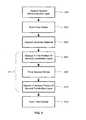
- FIG. 3shows a process flow diagram for an exemplary process for forming module 100.
- the processincludes the formation of a thin film stack forming cell 107, wherein the films or layers are formed on superstrate 201 (shown from the top down in FIG. 2 ).
- superstrate 201is provided (box 301).
- Superstrate 201may be fabricated from any suitable material capable of receiving thin films for use as photovoltaic cells and sufficiently transparent to allow transmission of light 105.
- first conductive layer 203is deposited onto superstrate 201 (box 303).
- First conductive layer 203is electrically conductive, which permits electrical conduction to provide the series arrangement of cells 107. While not so limited, in one embodiment, first conductive layer 203 may be formed to a thickness of about 0.1-0.7 ⁇ m or 0.1-0.4 ⁇ m or 0.2-0.3 ⁇ m or 0.2-1.0 ⁇ m or 0.3-0.7 ⁇ m or 0.35-0.55 ⁇ m of tin oxide.
- first conductive layer 203can be formed, for example, by direct current (DC) or radio frequency (RF) sputtering.
- first conductive layer 203is a layer of tin oxide substantially amorphous Cd 2 SnO 4 that is deposited with chemical vapor deposition (CVD) onto superstrate 201.
- CVDchemical vapor deposition
- buffer layer 205may be applied to first conductive layer 203 (box 305).
- buffer layer 205may be formed, for example, by sputtering.
- buffer layer 205may be formed by sputtering from a hot-pressed target containing, for example, primarily Sn and 1-22% Zn by weight or stoichiometric amounts of about 67 mol % SnO 2 and about 33 mol % ZnO onto first conductive layer 203.
- the zinc tin oxide material for buffer layer 205may be substantially amorphous.
- Buffer layer 205may have a thickness of between about 20 and 300 nm (200 and 3,000 Angstroms), or between about 80 and 150 nm (800 and 1,500 Angstroms), in order to have desirable mechanical, optical, and electrical properties. Buffer layer 205 may have a wide optical bandgap, for example about 3.3 eV or more, in order to permit the transmission of light 105.
- First semiconductor layer 207is deposited on buffer layer 205 (box 307).
- first semiconductor layer 207may be formed, for example, by chemical bath deposition or sputtering. While not so limited, first semiconductor layer 207 may be deposited to a thickness of from about 0.01 to about 0.3 ⁇ m or about 0.01 to about 0.12 ⁇ m or 0.03 to 0.1 ⁇ m or 0.05 to 0.9 ⁇ m or about 0.08 ⁇ m.
- One suitable material for use as first semiconductor layer 207may include CdS. A suitable thickness for a CdS layer may range from about 50 to 80 nm (500 to 800 Angstroms).
- First semiconductor layer 207forms the junction with second semiconductor layer 209 to create the photovoltaic effect in cell 107, allowing cell 107 to produce electricity from light 105.
- second semiconductor layer 209is deposited on first semiconductor layer 207 (box 309).
- Second semiconductor layer 209may include Cd, CdTe or other p-type semiconductor material.
- Second semiconductor layer 209may be deposited by diffusive transport deposit, sputtering or other suitable deposition method for depositing p-type semiconductor thin film material.
- Second conductive layer 211may be fabricated from any suitable conductive material. Second conductive layer 211 may be formed by sputtering, electrodeposition, screen printing, physical vapor deposition (PVD), chemical vapor deposition (CVD) or spraying. In one embodiment, second conductive layer 211 is a combination of graphite that is screen printed onto the surface and nickel and aluminum alloy that is sputtered thereon.
- All the sputtering steps described abovemay be magnetron sputtering at ambient temperature under highly pure atmospheres.
- a zinc tin oxide buffer layer 205may be formed by DC sputtering.
- other deposition processesmay be used, including higher temperature sputtering, electrodeposition, screen printing, physical vapor deposition (PVD), chemical vapor deposition (CVD) or spraying.
- the processingmay be provided in a continuous line or may be a series of batch operations. When the process is a continuous process, the sputtering or deposition chambers are individually isolated and brought to coating conditions during each coating cycle, then repeated.
- Encapsulating glass 213is adhered to second conductive layer 211 (box 313).
- Encapsulating glass 213may be a rigid material suitable for use with thin film structures and may be the same material or different material than superstrate 201.
- Encapsulating glass 213may be adhered to second conductive layer 211 using any suitable method. For example, encapsulating glass 213 may be adhered to second conductive layer 211 using an adhesive or other bonding composition.
- module 100 and cells 107may be included in the process for forming module 100 and cells 107.
- cleaning, etching, doping, dielectric or other selective insulative material deposition, formation of interfacial layers, scribing, heat treatments, and wiringmay also be utilized.
- wiring and/or bussing devicesmay be provided to complete the PV circuit (i.e., cells 107 in series arrangement) and to provide connectivity of the PV circuit to a load or other external device.
- Scribingmay be utilized to form the interconnections between the layers and to isolate cells and/or layers of the thin film stack. Scribing may be accomplished using any known technique for scribing and/or interconnecting the thin film layers. In one embodiment, scribing is accomplished using a laser directed at one or more layers from one or more directions. One or more laser scribes may be utilized to selectively remove thin film layers and to provide interconnectivity and/or isolation of cells 107. In one embodiment, the scribes and layer deposition are accomplished to interconnect and/or isolate cells 107 to provide a PV circuit having cells 107 in a series of electrical arrangements.
- FIG. 4shows an enlarged area 400 from FIG. 1 .
- cellsare divided by interconnections 401.
- the interconnections 401may be any suitable structures for forming the electrical interconnection between cells 107. Suitable structures may include spacing or scribes, dielectric material, insulating material, wiring, conductive material or other suitable material for forming the electrical connection between cells 107.
- FIG. 5illustrates a side view of an exemplary film stack for interconnection 401 taken in direction 5-5 of FIG. 4 .
- the interconnection 401includes structures formed between cells 107.
- the interconnection 401includes a first scribe 503, a second scribe 505 and a third scribe 507.
- First scribe 503, second scribe 505 and third scribe 507 of interconnection 401are formed during the formation of the cell 107 (see method of FIG. 3 ).
- FIG. 6includes a flowchart illustrating an exemplary method for forming interconnection 401.
- the methodincludes depositing second semiconductor layer 209 (box 309), as shown and described with respect to box 309 of FIG. 3 .
- first scribe 503is formed subsequent to the deposition of the second semiconductor layer (box 603) and may be formed by directing an energy source, for example in the form of concentrated electromagnetic energy, or a beam through superstrate 201 to selectively remove the layers present thereon.
- Suitable energy sourcesmay include, but are not limited to, laser, radio frequency (Rf), electron beam, ion beam, infrared (IR) or source for rapid thermal process (RTA).
- the scribemay be formed by chemical processes, such as photolithography.
- the first scribe 503is filled with dielectric material 509 (box 605). Suitable dielectric materials may include, but are not limited to a negative photo resist or other suitable dielectric material.
- the method for forming interconnection 401further includes formation of the second scribe 505 during the deposition of the second conductive layer 211 (box 609 of FIG. 6 , box 311 of FIG. 3 ).
- This stepincludes depositing a first portion 511 of second conductive layer 211.
- This first portion 511may include any suitable conductive material. Suitable first portion 511 may include, for example, graphite.
- the second scribe 505may be formed by directing concentrated electromagnetic energy or a beam from an energy source through superstrate 201 to selectively remove the layers present thereon (box 609).
- the energy sourcemay be any suitable energy source and may include the same or different source utilized to form first scribe 503.
- a second portion 513 of the second conductive layer 211is provided (box 611).
- the second portion 513may be any suitable conductive material and may include, for example, metal alloys, such as Ni and Al containing alloys.
- metal alloyssuch as Ni and Al containing alloys.
- a first portion 511 containing a graphite layeris provided prior to the second scribe 505 and a second portion 513 a metal layer is provided after the second scribe 505 is formed.
- the second portion 513is also deposited onto surfaces formed by the second scribe 505.
- the second portion 513 of the second conductive layer 211is electrically conductive, the second portion electrically connects the first conductive layer 203 and buffer layer 205 to the second conductive layer 211. This connection (upon isolation with the third scribe 507, see below) places the cells 107 into a series arrangement.
- the third scribe 507is formed subsequent to the deposition of the second conductive layer 211 (box 613).
- the third scribe 507may be formed by directing concentrated electromagnetic energy from an energy source onto the layers from the direction opposite the superstrate 201 to selectively remove the layers present thereon.
- the energy sourcemay be any suitable energy source and may include the same or different source utilized to form first scribe 503.
- Third scribe 507severs the first conductive layer 211, the first semiconductor layer 207 and the second semiconductor layer 209, but permits the buffer layer 205 and the first conductive layer 203 to remain (see e.g., FIG. 5 ).
- the arrangement of the module 100 remaining after the third scribe 507is a series arrangement of cells 107.
- the second scribe 505 formed after the deposition of the first portion 511 of the second conductive layer 211results in a space that extends to the first conductive layer 203 (see e.g., FIG. 5 ).
- reduced conductive area 501is formed on the first conductive layer 203.
- the reduced conductive area 501is an area in which the material of the first conductive layer 203 is at least partially chemically reduced.
- the reduced conductive area 501may be located along the first conductive layer 203.
- the positioning of the reduced conductive area 501may be such that the reduced conductive area 501 occupies the dead areas of module 100 that do not generate electricity, wherein any opacity or lack of transparency in the reduced conductive area 501 does not affect the performance of the module 100.
- the increased conductivity or reduced resistivity of the first conductive layer 203 in the area of the reduced conductive area 501increases the efficiency and/or performance of the module 100.
- FIG. 7includes a flowchart illustrating an exemplary method for forming reduced conductive area 501.
- the methodincludes providing a transparent, electrically conductive, reducible material (box 701).
- the reducible materialmay, for example, be a first conductive layer 203 including transparent conductive oxide (TCO) material.
- Suitable reducible materialmay include SnO 2 , In 2 O 3 , Cd 2 SnO 4 ZnO, other reducible material and combinations thereof.
- the methodfurther includes providing a reducing atmosphere (box 703).
- the reducing atmospheremay include gas such as, for example, hydrogen, carbon monoxide, reforming gas or other suitable reducing gas.
- An exemplary reducing atmospheremay include a combination of carbon monoxide and forming gas (4-5% H 2 , 95-96% N 2 ) ambient gas composition.
- the reducing atmospheremay include a gas additive to provide desirable material properties in the formed reduced conductive area 501.
- the reduced conductive area 501may include reduced gas additive.
- the gas additiveis provided to reduce or eliminate the amount of volume change that may result from the reduction or exposure to heat.
- Suitable gas additivesmay include organometallic gasses such as tin tetrachloride, dimethyl cadmium, dimethyl zinc or combinations thereof.
- An energy sourcesuch as a laser, is directed toward the reducible material in the form of concentrated electromagnetic energy (box 705).
- the laser or other energy sourceis configured to generate concentrated electromagnetic energy with a power density and/or wavelength that provides heat and energy to the reducible material.
- the reduced conductive area 501 where concentrated electromagnetic energy 803 from the energy source 801 (see e.g., FIG. 8 ) contacts the reducible material in the reducing atmosphereincludes conditions that facilitate reduction of the reducible material to form the reduced conductive area 501 (box 707).
- the reduced conductive area 501includes an electrical conductivity that is greater than the conductivity of the reducible material.
- FIG. 8illustrates an apparatus for forming the reduced conductive area 501 as shown and described in FIG. 7 .
- an energy source 801emits concentrated electromagnetic energy 803 that is directed at surface 805 of first conductive layer 203.
- the energy source 801may be an energy source capable of providing sufficient heat to the surface 805 of the first conductive layer 203 to at least partially reduce the first conductive layer 203.
- the processis accomplished in a chamber 807 that is capable of providing a reducing atmosphere 809 at the surface 805.
- concentrated electromagnetic energy 803 contacts the surface 805 in the presence of the reducing atmospherethe first conductive layer 203 is at least partially reduced to form a reduced conductive area 501.
- the reduced conductive area 501is metallic.
- the reduced conductive area 501is at least partially opaque. In these embodiments, the positioning of the reduced conductive area 501 is such that the opacity is in areas that do in impede sunlight and/or does not substantially affect the operation of the module 100.
- FIG. 9shows another embodiment, wherein a reduced conductive area 501 is formed when the second scribe 505 is being formed (box 609 of FIG. 6 ).
- the energy source 801includes concentrated electromagnetic energy 803, such as a laser beam, that is directed through superstrate 201, wherein the first portion 511 of first conductive layer 203, buffer layer 205, the first semiconductor layer 207, second semiconductor layer 209 and second conductive layer 211 are selectively removed.
- Concentrated electromagnetic energy 803provides heat to surface 805 of first conductive layer 203.
- a reducing atmosphere 809is provided to surface 805, resulting in formation of reduced conductive area 501 on first conductive layer 203.
Landscapes
- Photovoltaic Devices (AREA)
Description
- The present invention is directed generally to thin film articles having transparent conductive films and methods for modifying transparent conductive films.
- Energy demand is constantly increasing. As the energy demand increases, sources alternative to fossil fuel energy sources increase in importance. One such alternative energy source is solar energy. Generally, solar energy is produced by converting radiation (for example, sunlight) into electricity which may be stored or transmitted through electrical power grids.
- Transparent conductive oxides (TCOs) are used as electrically conductive layers for the electrical contact of thin film photovoltaic (PV) cells in a PV module on a side that receives sunlight during operation. During processing, interconnections between cells are provided using thin film application methods and scribing techniques, using chemicals or lasers to selectively remove material. As a result of the processing and the structures forming the interconnections, the area of interconnection between cells is a "dead area" (i.e., no light collection) and does not generate electricity.
- In addition, the interconnection between conductive layers is a large contributor to series resistance in a PV module. Therefore, it is desirable to decrease the resistivity of the area of interconnections between PV cells.
- Baik S J et al entitled: "Highly Textured and Conductive Undoped ZnO Film Using Hydrogen Post-Treatment" discloses a method comprising depositing a ZnO film using a MOCVD apparatus, for use as a transparent electrode in thin-film solar cells. H2 post-treatment of the ZNO film, using a mercury-sensitized photo-CVD system and a low-pressure mercury lamp whilst flowing H2, is disclosed as decreasing resistivity without degradation of total transmittance.
WO-A-2004/006293 concerns a method of annealing electrically conductive ZnO film to improve electrical conductivity thereof. The layer is annealed at high temperature in an inert atmosphere having sufficient levels of entrained ZnO to permit reduction of oxygen levels while maintaining zinc levels in the lattice structure.WO-A-2009/058385 concerns methods for forming a transparent conductive oxide coating for thin film PV applications. A layer of transparent conductive oxide is formed on a substrate at an elevated temperature, and then cooled in a non-oxidizing, or slightly reducing, atmosphere to improve electrical conductivity of the coating.- A method for producing an article that has decreased resistivity/increased conductivity in the interconnection between cells, without affecting the active area of the PV cells would be desirable.
- One aspect of the present disclosure thus includes a method for forming a reduced conductive area in transparent conductive films as defined in appended
claim 1. - The present disclosure also describes a thin film article having selectively modified electrical conductivity. The article includes a substrate having a transparent, electrically conductive, chemically reducible material and a reduced conductive area selectively disposed within the electrically conductive, chemically reducible material. The reduced conductive area has greater electrical conductivity than the transparent, electrically conductive, chemically reducible material.
- The present disclosure further describes a thin film photovoltaic module having a transparent conductive oxide layer. The module includes a reduced conductive area selectively disposed within the transparent conductive oxide layer. The reduced conductive area has greater electrical conductivity than the transparent conductive oxide layer.
- Other features and advantages of the present invention will be apparent from the following more detailed description of the preferred embodiments, taken in conjunction with the accompanying drawings which illustrate, by way of example, the principles of the invention, in which:
FIG. 1 shows a thin film module mounted on a base according to the disclosure.FIG. 2 is a diagram of a layer system making up cells of a module according to the disclosure.FIG. 3 is a process flow diagram for an exemplary process for forming a module according to the disclosure.FIG. 4 shows an enlargedarea 400 of the thin film module ofFIG. 1 .FIG. 5 shows a sectional view taken in direction 5-5 ofFIG. 4 .FIG. 6 is a process flow diagram for an exemplary process for forming an interconnection according to the disclosure.FIG. 7 is a process flow diagram for an exemplary process for forming a reduced conductive area.FIG. 8 is an apparatus for forming a reduced conductive area according to the disclosure.FIG. 9 is an apparatus for forming a reduced conductive area in a PV cell according to the disclosure.- Wherever possible, the same reference numbers will be used throughout the drawings to represent the same parts.
- Provided is a method for producing an article that has decreased resistivity/increased conductivity in the interconnection between cells, without substantially affecting the active area of the PV cells. Embodiments of the present disclosure may result in articles having decreased resistivity in the interconnection area between cells and increased overall module efficiency. In addition, other embodiments may permit the laser scribing of the interconnection in a controlled environment during interconnection formation in the presence of a readily available oxygen-reducing gas such as forming gas or carbon monoxide, which decreases the series resistance of the module. The system and method of the present disclosure may increase the PV module efficiency, without complicated or expensive equipment or processes.
- In the disclosure, when a layer is being described as "adjacent", "on" or "over" another layer or substrate, it is to be understood that the layer can either be directly in contact or that another layer or feature can intervene. In addition, "dead area" includes an area across the PV module that does not produce electricity when exposed to light. For example a dead area may include an area having no material that produces electricity or may include electricity producing layers that are electrically isolated. Conversely, "active area" includes an area across the PV module that produces electricity when exposed to light and is connectable to a load. When a layer or material is described as "transparent", it is to be understood that a transparent film includes materials that are fully or partially transparent to light at some or all wavelengths found in natural sunlight. When a layer or material is described as "electrically conductive" or "conductive" or is a "conductor" it is to be understood that the material permits the flow of electricity with or without electrical resistance. When a layer or material is described as "electrically insulative", "insulative" or is an "insulator" it is to be understood that the material impedes or prevents the flow of electricity. "Reduced", "reducing", "reduction" and other grammatical variations thereof refer to chemical reduction of a material wherein a gain of electrons or a decrease in oxidation state by a molecule, atom or ion takes place. In particular, reduction may include the chemical removal of oxygen from an oxide to form a metallic or partially metallic material. "Modifying", "modify" and other grammatical variations thereof with respect to layers, articles and materials refer to a change, such as a chemical change, in the material resulting in properties that are different than the original material.
- One embodiment of the disclosure includes a method for converting a transparent conductive layer, typically a transparent conductive oxide layer (TCO), in the dead area of a PV module to a higher conductivity metal. The conversion process may include a chemical reduction process that removes oxygen from the TCO. The method through which the TCO is converted is through the alleviation of oxygen in the films when heated by laser in the presence of an oxygen-attracting gas such as hydrogen, forming gas or carbon monoxide.
FIG. 1 shows a thinfilm PV module 100 mounted on abase 103. The PV module is arranged to receivelight 105. The PV module is divided into a plurality ofcells 107 that are arranged in series. Thecells 107 are divided by spaces, non-conductive material and/or other structures separating circuits. For example,cells 107 may be isolated from each other by scribes formed by laser scribing. When thePV module 100 is exposed tolight 105, electricity is produced. The disclosure is not limited to the arrangement shown and may include other mounting arrangements and/orcells 107. For example, thecells 107 may be oriented along the long dimension ofmodule 100 instead of the short dimension ofmodule 100. One embodiment of the disclosure includes a thin film CdTe solar photovoltaic (PV) module. Such modules are used to produce solar electricity for numerous applications, for example, large ground-mounted systems and rooftop systems on commercial and residential buildings. While the PV module may be a thin film structure, the method and system of the present disclosure may also be utilized to form gridline front contacts on crystalline solar cells such as, Si or Group III-V-based concentrators (e.g., GaAs, and GaInP).FIG. 2 is a diagram of the layersystem forming cells 107 ofPV module 100. The layers ofcell 107 include asuperstrate 201, a firstconductive layer 203, abuffer layer 205, afirst semiconductor layer 207, asecond semiconductor layer 209, a secondconductive layer 211 and anencapsulating glass 213. The layers of thecell 107 are arranged to generate and conduct electricity in a usable form when exposed tolight 105.- The
superstrate 201 is a sheet of high transmission glass onto which thin films are grown. The superstrate receives the light 105 (seeFIG. 1 ) prior to the underlying layers.Superstrate 201 may be standard soda-lime glass, a high-transmission, low-iron float glass or any other suitable glass material having a high transmission rate forlight 105. In another embodiment, thesuperstrate 201 may also be a high transmission borosilicate glass. - After the light 105 passes through
superstrate 201, at least a portion of the light 105 passes through firstconductive layer 203. Firstconductive layer 203 may be a transparent conductive oxide (TCO), which permits transmission of light 105 with little or no absorption. The firstconductive layer 203 is also electrically conductive, which permits electrical conduction to provide the series arrangement of cells. The firstconductive layer 203 is formed to a thickness that provides electrical conductivity, but permits the passage of at least some light 105. While not so limited, in one embodiment, the firstconductive layer 203 may be formed to a thickness of about 0.1-0.7 µm or 0.1-0.4 µm or 0.2-0.3 µm or 0.2-1.0 µm or 0.3-0.7 µm or 0.35-0.55 µm of tin oxide. One suitable material for use in formation of the firstconductive layer 203 may be fluorine-doped tin oxide. - Other suitable conductive layers may include, for example, stoichiometric cadmium stannate (nominally Cd2SnO4), aluminum-doped zinc oxide, indium tin oxide, doped indium oxide, zinc or cadmium doped tin oxide, copper aluminum oxides or another compound of cadmium tin oxide (such as CdSnO3). First
conductive layer 203 may permit passage of light 105 through to the semiconductor layers (e.g.,first semiconductor layer 207 and second semiconductor layer 209) while also functioning as an ohmic electrode to transport photogenerated charge carriers away from the light absorbing material. - A
buffer layer 205 is adjacent to firstconductive layer 203.Buffer layer 205 is more electrically resistive and protects the layers ofcell 107 from chemical interactions from the glass and/or interactions which might be incurred from subsequent processing. Inclusion ofbuffer layer 205 reduces or prevents electrical or other losses that may take place acrosscell 107 and acrossmodule 100. Suitable materials forbuffer layer 205 may include tin oxide containing materials, such as, but not limited to, zinc doped tin oxide, a mixture of zinc and tin oxides (for example zinc tin oxide having 0.5 to 33 atomic % Zn), zinc stannate, gallium oxide, aluminum oxide, silicon oxide, indium oxide, cadmium oxide and any other suitable barrier material having more electrical resistivity than firstconductive layer 203 and the capability of protecting the layers of the cell from interactions from the glass or interactions from subsequent processing. In addition, the inclusion ofbuffer layer 205 permits the formation of afirst semiconductor layer 207 which permits photon passage while maintaining a high quality junction capable of generating electricity. In certain embodiments,buffer layer 205 may be omitted or substituted by another material or layer. In one embodiment,buffer layer 205 includes a combination of ZnO and SnO2. For example, in one embodiment, thebuffer layer 205, while not so limited, may be formed to a thickness of up to about 1.5 microns or about 0.8-1.5 microns and may include ZnO and SnO2 having about 1 to 22 wt% Zn and Zn to Sn ratios from about 1:60 to 1:2 or from about 1:5 to about 1:18 or about 1:10. Other suitable Zn to Sn ratios may include 0:1 to 1:2 or about 0:0.5. - As shown in
FIG. 2 ,first semiconductor layer 207 is adjacent to bufferlayer 205 and receives light 105 subsequent to superstrate 201, firstconductive layer 203 andbuffer layer 205.First semiconductor layer 207 includes a wide bandgap n-type semiconductor material. Suitable semiconductor material forfirst semiconductor layer 207 includes, but is not limited to CdS, SnO2, CdO, ZnO, AnSe, GaN, In2O2, CdSnO, ZnS, CdZnS or other suitable n-type semiconductor material. In one embodiment thefirst semiconductor layer 207 includes CdS. While not so limited,first semiconductor layer 207 may have a thickness from about 0.01 to about 0.12 µm or 0.03 to 0.1 µm or 0.05 to 0.9 µm or about 0.08 µm.First semiconductor layer 207 may be formed by chemical bath deposition or by sputtering.First semiconductor layer 207 preferably has a smooth surface and is substantially uniform and free of impurities and pinholes. First semiconductor layer 207 forms the junction with asecond semiconductor layer 209 to create the photovoltaic effect incell 107, allowing electricity to be generated fromlight 105.Second semiconductor layer 209 may include, for example, Cd, CdTe or other p-type semiconductor material. Whensecond semiconductor layer 209 is provided with first semiconductor layer 207 a photovoltaic effect results when exposed tolight 105.- As shown in
FIG. 2 ,second semiconductor layer 209 is adjacent tofirst semiconductor layer 207. A secondconductive layer 211 is adjacent to thesecond semiconductor layer 209 and provides an electrically conductive material that is capable of conducting electricity formed from the combination of thefirst semiconductor layer 207 andsecond semiconductor layer 209 when exposed tolight 105. AlthoughFIG. 2 shows an arrangement of two layers forfirst semiconductor layer 207 andsecond semiconductor layer 209, any number of layers, including interfacial layers, may be utilized to provide the photovoltaic effect. - Second
conductive layer 211 may be fabricated from any suitable conductive material and combinations thereof. For example, suitable materials may include materials including, but not limited to, graphite, metallic silver, nickel, copper, aluminum, titanium, palladium, chrome, molybdenum alloys of metallic silver, nickel, copper, aluminum, titanium, palladium, chrome, and molybdenum and any combination thereof. In one embodiment, secondconductive layer 209 may be a combination of graphite, nickel and aluminum alloys. - An encapsulating
glass 213 may be adhered adjacent to secondconductive layer 211. Encapsulatingglass 213 may be a rigid structure suitable for use with the thin films ofcell 107. Encapsulatingglass 213 may be the same material assuperstrate 201 or may be different. In addition, although not shown inFIG. 2 , encapsulatingglass 213 may include openings or structures to permit wiring and/or connection tocell 107. Module 100 andindividual cells 107 may include other layers and structures not shown inFIG. 2 . For example,superstrate 201 and/or encapsulatingglass 213 may include a barrier coating or other structure in order to reduce or prevent diffusion of impurities into the layers. In addition, encapsulatingglass 213 may include an adherent layer to adhere encapsulatingglass 213 to the layers. Additional structures that may be present inmodule 100 and/orcells 107 include, for example, scribes, bussing structures, external wiring, and various conventional components useful with thin film and/or PV structures.FIG. 3 shows a process flow diagram for an exemplary process for formingmodule 100. The process includes the formation of a thin filmstack forming cell 107, wherein the films or layers are formed on superstrate 201 (shown from the top down inFIG. 2 ).- As shown in the flow diagram of
FIG. 3 ,superstrate 201 is provided (box 301).Superstrate 201 may be fabricated from any suitable material capable of receiving thin films for use as photovoltaic cells and sufficiently transparent to allow transmission oflight 105. - Subsequent to providing
superstrate 201, firstconductive layer 203 is deposited onto superstrate 201 (box 303). Firstconductive layer 203 is electrically conductive, which permits electrical conduction to provide the series arrangement ofcells 107. While not so limited, in one embodiment, firstconductive layer 203 may be formed to a thickness of about 0.1-0.7 µm or 0.1-0.4 µm or 0.2-0.3 µm or 0.2-1.0 µm or 0.3-0.7 µm or 0.35-0.55 µm of tin oxide. Other suitable conductive layers may include fluorine-doped stoichiometric cadmium stannate (nominally Cd2SnO4), aluminum-doped zinc oxide, indium tin oxide, doped indium oxide, zinc or cadmium doped tin oxide, copper aluminum oxides or another compound of cadmium tin oxide (such as CdSnO3). Firstconductive layer 203 can be formed, for example, by direct current (DC) or radio frequency (RF) sputtering. In one embodiment, firstconductive layer 203 is a layer of tin oxide substantially amorphous Cd2SnO4 that is deposited with chemical vapor deposition (CVD) ontosuperstrate 201. Such CVD can be performed from tin and fluorine containing precursors in an oxygen containing environment. - Once first
conductive layer 203 is applied,buffer layer 205 may be applied to first conductive layer 203 (box 305). In one embodiment,buffer layer 205 may be formed, for example, by sputtering. In one example,buffer layer 205 may be formed by sputtering from a hot-pressed target containing, for example, primarily Sn and 1-22% Zn by weight or stoichiometric amounts of about 67 mol % SnO2 and about 33 mol % ZnO onto firstconductive layer 203. When deposited by sputtering, the zinc tin oxide material forbuffer layer 205 may be substantially amorphous.Buffer layer 205 may have a thickness of between about 20 and 300 nm (200 and 3,000 Angstroms), or between about 80 and 150 nm (800 and 1,500 Angstroms), in order to have desirable mechanical, optical, and electrical properties.Buffer layer 205 may have a wide optical bandgap, for example about 3.3 eV or more, in order to permit the transmission oflight 105. First semiconductor layer 207 is deposited on buffer layer 205 (box 307). In one embodiment,first semiconductor layer 207 may be formed, for example, by chemical bath deposition or sputtering. While not so limited,first semiconductor layer 207 may be deposited to a thickness of from about 0.01 to about 0.3 µm or about 0.01 to about 0.12 µm or 0.03 to 0.1 µm or 0.05 to 0.9 µm or about 0.08 µm. One suitable material for use asfirst semiconductor layer 207 may include CdS. A suitable thickness for a CdS layer may range from about 50 to 80 nm (500 to 800 Angstroms).First semiconductor layer 207 forms the junction withsecond semiconductor layer 209 to create the photovoltaic effect incell 107, allowingcell 107 to produce electricity fromlight 105.- After the formation of
first semiconductor layer 207,second semiconductor layer 209 is deposited on first semiconductor layer 207 (box 309).Second semiconductor layer 209 may include Cd, CdTe or other p-type semiconductor material.Second semiconductor layer 209 may be deposited by diffusive transport deposit, sputtering or other suitable deposition method for depositing p-type semiconductor thin film material. - Subsequent to the formation of the
second semiconductor layer 209, secondconductive layer 211 is formed (box 311). Secondconductive layer 211 may be fabricated from any suitable conductive material. Secondconductive layer 211 may be formed by sputtering, electrodeposition, screen printing, physical vapor deposition (PVD), chemical vapor deposition (CVD) or spraying. In one embodiment, secondconductive layer 211 is a combination of graphite that is screen printed onto the surface and nickel and aluminum alloy that is sputtered thereon. - All the sputtering steps described above may be magnetron sputtering at ambient temperature under highly pure atmospheres. For example, a zinc tin
oxide buffer layer 205 may be formed by DC sputtering. However, other deposition processes may be used, including higher temperature sputtering, electrodeposition, screen printing, physical vapor deposition (PVD), chemical vapor deposition (CVD) or spraying. In addition, the processing may be provided in a continuous line or may be a series of batch operations. When the process is a continuous process, the sputtering or deposition chambers are individually isolated and brought to coating conditions during each coating cycle, then repeated. - Once second
conductive layer 211 is formed, encapsulatingglass 213 is adhered to second conductive layer 211 (box 313). Encapsulatingglass 213 may be a rigid material suitable for use with thin film structures and may be the same material or different material thansuperstrate 201. Encapsulatingglass 213 may be adhered to secondconductive layer 211 using any suitable method. For example, encapsulatingglass 213 may be adhered to secondconductive layer 211 using an adhesive or other bonding composition. - Although not shown in
FIG. 3 , other processing steps may be included in the process for formingmodule 100 andcells 107. For example, cleaning, etching, doping, dielectric or other selective insulative material deposition, formation of interfacial layers, scribing, heat treatments, and wiring may also be utilized. For example, wiring and/or bussing devices may be provided to complete the PV circuit (i.e.,cells 107 in series arrangement) and to provide connectivity of the PV circuit to a load or other external device. - Scribing may be utilized to form the interconnections between the layers and to isolate cells and/or layers of the thin film stack. Scribing may be accomplished using any known technique for scribing and/or interconnecting the thin film layers. In one embodiment, scribing is accomplished using a laser directed at one or more layers from one or more directions. One or more laser scribes may be utilized to selectively remove thin film layers and to provide interconnectivity and/or isolation of
cells 107. In one embodiment, the scribes and layer deposition are accomplished to interconnect and/or isolatecells 107 to provide a PVcircuit having cells 107 in a series of electrical arrangements. FIG. 4 shows anenlarged area 400 fromFIG. 1 . As shown inFIG. 4 , cells are divided byinterconnections 401. Theinterconnections 401 may be any suitable structures for forming the electrical interconnection betweencells 107. Suitable structures may include spacing or scribes, dielectric material, insulating material, wiring, conductive material or other suitable material for forming the electrical connection betweencells 107.FIG. 5 illustrates a side view of an exemplary film stack forinterconnection 401 taken in direction 5-5 ofFIG. 4 . As shown inFIG. 5 , theinterconnection 401 includes structures formed betweencells 107. As shown inFIG. 5 , theinterconnection 401 includes afirst scribe 503, asecond scribe 505 and athird scribe 507.First scribe 503,second scribe 505 andthird scribe 507 ofinterconnection 401 are formed during the formation of the cell 107 (see method ofFIG. 3 ).FIG. 6 includes a flowchart illustrating an exemplary method for forminginterconnection 401. The method includes depositing second semiconductor layer 209 (box 309), as shown and described with respect tobox 309 ofFIG. 3 . Specifically,first scribe 503 is formed subsequent to the deposition of the second semiconductor layer (box 603) and may be formed by directing an energy source, for example in the form of concentrated electromagnetic energy, or a beam throughsuperstrate 201 to selectively remove the layers present thereon. Suitable energy sources may include, but are not limited to, laser, radio frequency (Rf), electron beam, ion beam, infrared (IR) or source for rapid thermal process (RTA). In another embodiment, the scribe may be formed by chemical processes, such as photolithography. To provide electrical isolation, thefirst scribe 503 is filled with dielectric material 509 (box 605). Suitable dielectric materials may include, but are not limited to a negative photo resist or other suitable dielectric material.- The method for forming
interconnection 401 further includes formation of thesecond scribe 505 during the deposition of the second conductive layer 211 (box 609 ofFIG. 6 ,box 311 ofFIG. 3 ). This step includes depositing afirst portion 511 of secondconductive layer 211. Thisfirst portion 511 may include any suitable conductive material. Suitablefirst portion 511 may include, for example, graphite. After thefirst portion 511 is formed, thesecond scribe 505 may be formed by directing concentrated electromagnetic energy or a beam from an energy source throughsuperstrate 201 to selectively remove the layers present thereon (box 609). The energy source may be any suitable energy source and may include the same or different source utilized to formfirst scribe 503. Subsequent to formation ofsecond scribe 505, asecond portion 513 of the secondconductive layer 211 is provided (box 611). Thesecond portion 513 may be any suitable conductive material and may include, for example, metal alloys, such as Ni and Al containing alloys. For example, in one embodiment afirst portion 511 containing a graphite layer is provided prior to thesecond scribe 505 and a second portion 513 a metal layer is provided after thesecond scribe 505 is formed. In addition to providing thesecond portion 513 to thecell 107, thesecond portion 513 is also deposited onto surfaces formed by thesecond scribe 505. Since thesecond portion 513 of the secondconductive layer 211 is electrically conductive, the second portion electrically connects the firstconductive layer 203 andbuffer layer 205 to the secondconductive layer 211. This connection (upon isolation with thethird scribe 507, see below) places thecells 107 into a series arrangement. - The
third scribe 507 is formed subsequent to the deposition of the second conductive layer 211 (box 613). Thethird scribe 507 may be formed by directing concentrated electromagnetic energy from an energy source onto the layers from the direction opposite thesuperstrate 201 to selectively remove the layers present thereon. The energy source may be any suitable energy source and may include the same or different source utilized to formfirst scribe 503.Third scribe 507 severs the firstconductive layer 211, thefirst semiconductor layer 207 and thesecond semiconductor layer 209, but permits thebuffer layer 205 and the firstconductive layer 203 to remain (see e.g.,FIG. 5 ). The arrangement of themodule 100 remaining after thethird scribe 507 is a series arrangement ofcells 107. - The
second scribe 505 formed after the deposition of thefirst portion 511 of the second conductive layer 211 (see e.g.,box 609 inFIG. 6 ) results in a space that extends to the first conductive layer 203 (see e.g.,FIG. 5 ). In one embodiment of the present disclosure, reducedconductive area 501 is formed on the firstconductive layer 203. The reducedconductive area 501 is an area in which the material of the firstconductive layer 203 is at least partially chemically reduced. The reducedconductive area 501 may be located along the firstconductive layer 203. The positioning of the reducedconductive area 501 may be such that the reducedconductive area 501 occupies the dead areas ofmodule 100 that do not generate electricity, wherein any opacity or lack of transparency in the reducedconductive area 501 does not affect the performance of themodule 100. In addition, the increased conductivity or reduced resistivity of the firstconductive layer 203 in the area of the reducedconductive area 501 increases the efficiency and/or performance of themodule 100. FIG. 7 includes a flowchart illustrating an exemplary method for forming reducedconductive area 501. The method includes providing a transparent, electrically conductive, reducible material (box 701). The reducible material may, for example, be a firstconductive layer 203 including transparent conductive oxide (TCO) material. Suitable reducible material may include SnO2, In2O3, Cd2SnO4 ZnO, other reducible material and combinations thereof. The method further includes providing a reducing atmosphere (box 703). The reducing atmosphere may include gas such as, for example, hydrogen, carbon monoxide, reforming gas or other suitable reducing gas. An exemplary reducing atmosphere may include a combination of carbon monoxide and forming gas (4-5% H2, 95-96% N2) ambient gas composition. In another embodiment, the reducing atmosphere may include a gas additive to provide desirable material properties in the formed reducedconductive area 501. In this embodiment, the reducedconductive area 501 may include reduced gas additive. In one embodiment, the gas additive is provided to reduce or eliminate the amount of volume change that may result from the reduction or exposure to heat. Suitable gas additives may include organometallic gasses such as tin tetrachloride, dimethyl cadmium, dimethyl zinc or combinations thereof. An energy source, such as a laser, is directed toward the reducible material in the form of concentrated electromagnetic energy (box 705). The laser or other energy source is configured to generate concentrated electromagnetic energy with a power density and/or wavelength that provides heat and energy to the reducible material. The reducedconductive area 501 where concentratedelectromagnetic energy 803 from the energy source 801 (see e.g.,FIG. 8 ) contacts the reducible material in the reducing atmosphere includes conditions that facilitate reduction of the reducible material to form the reduced conductive area 501 (box 707). The reducedconductive area 501 includes an electrical conductivity that is greater than the conductivity of the reducible material.FIG. 8 illustrates an apparatus for forming the reducedconductive area 501 as shown and described inFIG. 7 . As shown inFIG. 8 , anenergy source 801 emits concentratedelectromagnetic energy 803 that is directed atsurface 805 of firstconductive layer 203. Theenergy source 801 may be an energy source capable of providing sufficient heat to thesurface 805 of the firstconductive layer 203 to at least partially reduce the firstconductive layer 203. The process is accomplished in achamber 807 that is capable of providing a reducingatmosphere 809 at thesurface 805. When concentratedelectromagnetic energy 803 contacts thesurface 805 in the presence of the reducing atmosphere, the firstconductive layer 203 is at least partially reduced to form a reducedconductive area 501. In one embodiment, the reducedconductive area 501 is metallic. In certain embodiments, the reducedconductive area 501 is at least partially opaque. In these embodiments, the positioning of the reducedconductive area 501 is such that the opacity is in areas that do in impede sunlight and/or does not substantially affect the operation of themodule 100.FIG. 9 shows another embodiment, wherein a reducedconductive area 501 is formed when thesecond scribe 505 is being formed (box 609 ofFIG. 6 ). In this embodiment, theenergy source 801 includes concentratedelectromagnetic energy 803, such as a laser beam, that is directed throughsuperstrate 201, wherein thefirst portion 511 of firstconductive layer 203,buffer layer 205, thefirst semiconductor layer 207,second semiconductor layer 209 and secondconductive layer 211 are selectively removed. Concentratedelectromagnetic energy 803 provides heat to surface 805 of firstconductive layer 203. In addition, a reducingatmosphere 809 is provided to surface 805, resulting in formation of reducedconductive area 501 on firstconductive layer 203.- While the above has been described with respect to photovoltaic modules and photovoltaic devices, the method, thin film structure and apparatus of the present disclosure are usable with other thin film devices. Other thin film devices usable with the present disclosure include, but are not limited to photo detectors, diode application, or thin film displays.
- While the invention has been described with reference to a preferred embodiment, it will be understood by those skilled in the art that various changes may be made and equivalents may be substituted for elements thereof without departing from the scope of the invention. In addition, many modifications may be made to adapt a particular situation or material to the teachings of the invention without departing from the essential scope thereof. Therefore, it is intended that the invention not be limited to the particular embodiment disclosed as the best mode contemplated for carrying out this invention, but that the invention will include all embodiments falling within the scope of the appended claims.
Claims (10)
- A method for forming a reduced conductive area (501) in transparent conductive films, the method comprising:providing a transparent, electrically conductive, chemically reducible material; andproviding a reducing atmosphere (809);characterised by:directing concentrated electromagnetic energy (803) from an energy source (801) toward a portion of the transparent, electrically conductive, chemically reducible material so as to form a reduced conductive area (501) selectively disposed within the transparent, electrically conductive, chemically reducible material;wherein the reduced conductive area (501) has greater electrical conductivity than the transparent, electrically conductive, chemically reducible material.
- The method of claim 1, wherein the reducible material is a transparent conductive oxide.
- The method of any preceding claim, wherein the transparent conductive oxide is selected from the group consisting of SnO2 In2O3, Cd2SnO4, ZnO and combinations thereof.
- The method of any preceding claim, wherein the transparent, electrically conductive, chemically reducible material is a conductive layer of a thin film photovoltaic module (100).
- The method of claim 4, wherein the portion of the transparent, electrically conductive, chemically reducible material is a dead area, that does not produce electricity when exposed to light.
- The method of any preceding claim, wherein the reducing atmosphere (809) includes a gas selected from the group consisting of hydrogen, carbon monoxide, reforming gas and combinations thereof.
- The method of any preceding claim, wherein providing the reducing atmosphere (809) further comprises providing a gas additive.
- The method of claim 7, wherein the gas additive is an organometallic gas.
- The method of claim 8, wherein the organometallic gas is selected from the group consisting of tin tetrachloride, dimethyl cadmium, dimethyl zinc and combinations thereof.
- The method of any preceding claim, therein the concentrated electromagnetic energy (803) comprises a laser beam.
Applications Claiming Priority (1)
| Application Number | Priority Date | Filing Date | Title |
|---|---|---|---|
| US12/828,408US8525019B2 (en) | 2010-07-01 | 2010-07-01 | Thin film article and method for forming a reduced conductive area in transparent conductive films for photovoltaic modules |
Publications (2)
| Publication Number | Publication Date |
|---|---|
| EP2403015A1 EP2403015A1 (en) | 2012-01-04 |
| EP2403015B1true EP2403015B1 (en) | 2014-04-23 |
Family
ID=44510710
Family Applications (1)
| Application Number | Title | Priority Date | Filing Date |
|---|---|---|---|
| EP11172229.4ANot-in-forceEP2403015B1 (en) | 2010-07-01 | 2011-06-30 | Thin film article and method for forming a reduced conductive area in transparent conductive films for photovoltaic modules |
Country Status (4)
| Country | Link |
|---|---|
| US (2) | US8525019B2 (en) |
| EP (1) | EP2403015B1 (en) |
| CN (1) | CN102315325B (en) |
| AU (1) | AU2011203258B2 (en) |
Families Citing this family (5)
| Publication number | Priority date | Publication date | Assignee | Title |
|---|---|---|---|---|
| CN104334767B (en) | 2012-03-05 | 2017-06-09 | 第一太阳能有限公司 | Method and apparatus for forming transparent conductive oxides using hydrogen |
| US11978816B2 (en) | 2017-11-30 | 2024-05-07 | China Triumph International Engineering Co., Ltd. | Thin film device with additional conductive lines and method for producing it |
| EP3663433A1 (en)* | 2018-12-04 | 2020-06-10 | Nederlandse Organisatie voor toegepast- natuurwetenschappelijk onderzoek TNO | Method and system for depositing a p-type oxide layer on a substrate |
| CN113066897B (en)* | 2021-03-18 | 2022-02-22 | 西南石油大学 | Maskless preparation method of copper electrode of heterojunction solar cell |
| CN116960199B (en)* | 2023-09-20 | 2023-12-01 | 上海昕沐化学科技有限公司 | A method for manufacturing metal grid electrodes on heterojunction solar cells |
Family Cites Families (54)
| Publication number | Priority date | Publication date | Assignee | Title |
|---|---|---|---|---|
| US4104084A (en) | 1977-06-06 | 1978-08-01 | The United States Of America As Represented By The Administrator Of The National Aeronautics And Space Administration | Solar cells having integral collector grids |
| US4500567A (en)* | 1982-12-23 | 1985-02-19 | Nippon Sheet Glass Co., Ltd. | Method for forming tin oxide coating |
| JPS603164A (en)* | 1983-06-21 | 1985-01-09 | Sanyo Electric Co Ltd | Method of manufacturing photovoltaic device |
| US4754544A (en) | 1985-01-30 | 1988-07-05 | Energy Conversion Devices, Inc. | Extremely lightweight, flexible semiconductor device arrays |
| US4732621A (en) | 1985-06-17 | 1988-03-22 | Sanyo Electric Co., Ltd. | Method for producing a transparent conductive oxide layer and a photovoltaic device including such a layer |
| JPS6258685A (en)* | 1985-09-09 | 1987-03-14 | Fuji Electric Co Ltd | Manufacturing method of amorphous semiconductor solar cell |
| US4734381A (en)* | 1985-10-24 | 1988-03-29 | Atlantic Richfield Company | Method of making a thin film cadmium telluride solar cell |
| FR2639441A1 (en) | 1988-11-21 | 1990-05-25 | Saint Gobain Vitrage | BACK-ELECTRODE FOR ELECTROCHROME SYSTEMS |
| US5232519A (en)* | 1990-09-20 | 1993-08-03 | United Solar Systems Corporation | Wireless monolithic photovoltaic module |
| US5408109A (en) | 1991-02-27 | 1995-04-18 | The Regents Of The University Of California | Visible light emitting diodes fabricated from soluble semiconducting polymers |
| US5176758A (en) | 1991-05-20 | 1993-01-05 | United Solar Systems Corporation | Translucent photovoltaic sheet material and panels |
| US5221854A (en) | 1991-11-18 | 1993-06-22 | United Solar Systems Corporation | Protective layer for the back reflector of a photovoltaic device |
| JPH06140650A (en) | 1992-09-14 | 1994-05-20 | Sanyo Electric Co Ltd | Method of reforming light-transmitting conductive oxide film and manufacture of photosensor using the film |
| US5397920A (en) | 1994-03-24 | 1995-03-14 | Minnesota Mining And Manufacturing Company | Light transmissive, electrically-conductive, oxide film and methods of production |
| US6996150B1 (en) | 1994-09-14 | 2006-02-07 | Rohm Co., Ltd. | Semiconductor light emitting device and manufacturing method therefor |
| JPH10139428A (en)* | 1996-10-30 | 1998-05-26 | Mitsubishi Heavy Ind Ltd | Modification of tin dioxide film |
| US6137048A (en) | 1996-11-07 | 2000-10-24 | Midwest Research Institute | Process for fabricating polycrystalline semiconductor thin-film solar cells, and cells produced thereby |
| US6169246B1 (en) | 1998-09-08 | 2001-01-02 | Midwest Research Institute | Photovoltaic devices comprising zinc stannate buffer layer and method for making |
| US6121541A (en) | 1997-07-28 | 2000-09-19 | Bp Solarex | Monolithic multi-junction solar cells with amorphous silicon and CIS and their alloys |
| US6077722A (en) | 1998-07-14 | 2000-06-20 | Bp Solarex | Producing thin film photovoltaic modules with high integrity interconnects and dual layer contacts |
| US6365016B1 (en) | 1999-03-17 | 2002-04-02 | General Electric Company | Method and apparatus for arc plasma deposition with evaporation of reagents |
| US6517687B1 (en) | 1999-03-17 | 2003-02-11 | General Electric Company | Ultraviolet filters with enhanced weatherability and method of making |
| US6426125B1 (en) | 1999-03-17 | 2002-07-30 | General Electric Company | Multilayer article and method of making by ARC plasma deposition |
| US6261694B1 (en) | 1999-03-17 | 2001-07-17 | General Electric Company | Infrared reflecting coatings |
| US6420032B1 (en) | 1999-03-17 | 2002-07-16 | General Electric Company | Adhesion layer for metal oxide UV filters |
| JP4089113B2 (en) | 1999-12-28 | 2008-05-28 | 株式会社Ihi | Thin film production equipment |
| US6908782B2 (en) | 2000-08-18 | 2005-06-21 | Midwest Research Instittue | High carrier concentration p-type transparent conducting oxide films |
| US6548751B2 (en) | 2000-12-12 | 2003-04-15 | Solarflex Technologies, Inc. | Thin film flexible solar cell |
| DE60033038T2 (en) | 2000-11-24 | 2007-08-23 | Sony Deutschland Gmbh | Hybrid solar cell with thermally deposited semiconductor oxide layer |
| WO2003001602A2 (en) | 2001-06-21 | 2003-01-03 | Akzo Nobel N.V. | Manufacturing a solar cell foil connected in series via a temporary substrate |
| WO2004006293A2 (en) | 2001-08-15 | 2004-01-15 | Microcoating Technologies, Inc. | Method of annealing electrically conductive zinc oxide films |
| EP1289025A1 (en) | 2001-08-30 | 2003-03-05 | Universite De Neuchatel | Method to deposit an oxyde layer on a substrate and photovoltaic cell using such substrate |
| WO2003032406A2 (en) | 2001-10-05 | 2003-04-17 | Solar Systems & Equipments S.R.L. | A process for large-scale production of cdte/cds thin film solar cells |
| EP1443527A4 (en) | 2001-10-19 | 2007-09-12 | Asahi Glass Co Ltd | TRANSPARENT CONDUCTIVE OXIDE LAYER SUBSTRATE, PROCESS FOR PRODUCING THE SAME, AND PHOTOELECTRIC CONVERSION ELEMENT |
| FR2832811B1 (en) | 2001-11-28 | 2004-01-30 | Saint Gobain | TRANSPARENT TEXTURED PLATE WITH HIGH LIGHT TRANSMISSION |
| FR2833107B1 (en) | 2001-12-05 | 2004-02-20 | Saint Gobain | ELECTRODE OF ELECTROCHEMICAL / ELECTROCOMMANDABLE DEVICES |
| US6690041B2 (en)* | 2002-05-14 | 2004-02-10 | Global Solar Energy, Inc. | Monolithically integrated diodes in thin-film photovoltaic devices |
| JP4320564B2 (en)* | 2002-06-28 | 2009-08-26 | 日亜化学工業株式会社 | Transparent conductive film forming composition, transparent conductive film forming solution, and transparent conductive film forming method |
| EP1556902A4 (en) | 2002-09-30 | 2009-07-29 | Miasole | APPARATUS AND METHOD FOR MANUFACTURING CON CURRENT FOR LARGE SCALE PRODUCTION OF THIN FILM SOLAR CELLS |
| US7141863B1 (en) | 2002-11-27 | 2006-11-28 | University Of Toledo | Method of making diode structures |
| US20080105303A1 (en) | 2003-01-03 | 2008-05-08 | Bp Corporation North America Inc. | Method and Manufacturing Thin Film Photovoltaic Modules |
| US6936761B2 (en) | 2003-03-29 | 2005-08-30 | Nanosolar, Inc. | Transparent electrode, optoelectronic apparatus and devices |
| WO2005006393A2 (en)* | 2003-05-27 | 2005-01-20 | Triton Systems, Inc. | Pinhold porosity free insulating films on flexible metallic substrates for thin film applications |
| US7608294B2 (en)* | 2003-11-18 | 2009-10-27 | Nippon Sheet Glass Company, Limited | Transparent substrate with transparent conductive film, method of manufacturing the same, and photoelectric conversion element including the substrate |
| US7629236B2 (en)* | 2004-08-26 | 2009-12-08 | Alliance For Sustainable Energy, Llc | Method for passivating crystal silicon surfaces |
| US7394016B2 (en) | 2005-10-11 | 2008-07-01 | Solyndra, Inc. | Bifacial elongated solar cell devices with internal reflectors |
| US7259322B2 (en) | 2006-01-09 | 2007-08-21 | Solyndra, Inc. | Interconnects for solar cell devices |
| US7582161B2 (en) | 2006-04-07 | 2009-09-01 | Micron Technology, Inc. | Atomic layer deposited titanium-doped indium oxide films |
| JP5360789B2 (en) | 2006-07-06 | 2013-12-04 | 独立行政法人産業技術総合研究所 | P-type zinc oxide thin film and method for producing the same |
| JP2008165744A (en)* | 2006-12-07 | 2008-07-17 | Semiconductor Energy Lab Co Ltd | Semiconductor device |
| CA2704389A1 (en)* | 2007-11-02 | 2009-05-07 | Agc Flat Glass North America, Inc. | Transparent conductive oxide coating for thin film photovoltaic applications and methods of making the same |
| JPWO2009087848A1 (en)* | 2008-01-08 | 2011-05-26 | コニカミノルタホールディングス株式会社 | Dye-sensitized solar cell |
| KR100993513B1 (en)* | 2008-10-06 | 2010-11-10 | 엘지전자 주식회사 | Solar cell |
| US20110277816A1 (en)* | 2010-05-11 | 2011-11-17 | Sierra Solar Power, Inc. | Solar cell with shade-free front electrode |
- 2010
- 2010-07-01USUS12/828,408patent/US8525019B2/ennot_activeExpired - Fee Related
- 2011
- 2011-06-30EPEP11172229.4Apatent/EP2403015B1/ennot_activeNot-in-force
- 2011-07-01AUAU2011203258Apatent/AU2011203258B2/ennot_activeCeased
- 2011-07-01CNCN201110234999.2Apatent/CN102315325B/ennot_activeExpired - Fee Related
- 2013
- 2013-09-03USUS14/016,639patent/US20140000703A1/ennot_activeAbandoned
Also Published As
| Publication number | Publication date |
|---|---|
| US8525019B2 (en) | 2013-09-03 |
| US20140000703A1 (en) | 2014-01-02 |
| AU2011203258A1 (en) | 2012-01-19 |
| CN102315325B (en) | 2016-03-02 |
| CN102315325A (en) | 2012-01-11 |
| US20120000520A1 (en) | 2012-01-05 |
| EP2403015A1 (en) | 2012-01-04 |
| AU2011203258B2 (en) | 2016-03-24 |
Similar Documents
| Publication | Publication Date | Title |
|---|---|---|
| AU2010257207B2 (en) | Cadmium telluride thin film photovoltaic devices and methods of manufacturing the same | |
| CN102453863B (en) | Sputter the method based on the cadmium sulfide layer used in the film photovoltaic device of cadmium telluride | |
| CN102206801B (en) | The forming method of the conductive transparent oxide film layer used by film photovoltaic device based on cadmium telluride | |
| EP2383363B1 (en) | Cadmium sulfide layers for use in cadmium telluride based thin film photovoltaic devices and method of their manufacture | |
| CN102208485B (en) | Based on the formation method of the film photovoltaic device of cadmium telluride conductive transparent oxide rete used | |
| EP2403015B1 (en) | Thin film article and method for forming a reduced conductive area in transparent conductive films for photovoltaic modules | |
| CN102810581B (en) | The multi-layer N-type stack of film photovoltaic device based on cadmium telluride and manufacture method thereof | |
| EP2398045A2 (en) | Modified cadmium telluride layer, a method of modifying a cadmium telluride layer, and a thin film device having a cadmium telluride layer | |
| GB2405030A (en) | Bifacial thin film solar cell | |
| CN102208484B (en) | The forming method of the conductive transparent oxide film layer used by film photovoltaic device based on cadmium telluride | |
| CN102810597B (en) | Methods of forming a window layer in a cadmium telluride based thin film photovoltaic device | |
| CN102810593B (en) | The multi-layer N-type stack of film photovoltaic device and manufacture method thereof based on cadmium telluride | |
| US8460765B2 (en) | Methods for forming selectively deposited thin films | |
| EP2402994A1 (en) | Method and system for forming photovoltaic cell and a photovoltaic cell |
Legal Events
| Date | Code | Title | Description |
|---|---|---|---|
| AK | Designated contracting states | Kind code of ref document:A1 Designated state(s):AL AT BE BG CH CY CZ DE DK EE ES FI FR GB GR HR HU IE IS IT LI LT LU LV MC MK MT NL NO PL PT RO RS SE SI SK SM TR | |
| AX | Request for extension of the european patent | Extension state:BA ME | |
| PUAI | Public reference made under article 153(3) epc to a published international application that has entered the european phase | Free format text:ORIGINAL CODE: 0009012 | |
| 17P | Request for examination filed | Effective date:20120704 | |
| GRAP | Despatch of communication of intention to grant a patent | Free format text:ORIGINAL CODE: EPIDOSNIGR1 | |
| INTG | Intention to grant announced | Effective date:20131108 | |
| RAP1 | Party data changed (applicant data changed or rights of an application transferred) | Owner name:FIRST SOLAR MALAYSIA SDN.BHD | |
| GRAS | Grant fee paid | Free format text:ORIGINAL CODE: EPIDOSNIGR3 | |
| GRAA | (expected) grant | Free format text:ORIGINAL CODE: 0009210 | |
| AK | Designated contracting states | Kind code of ref document:B1 Designated state(s):AL AT BE BG CH CY CZ DE DK EE ES FI FR GB GR HR HU IE IS IT LI LT LU LV MC MK MT NL NO PL PT RO RS SE SI SK SM TR | |
| REG | Reference to a national code | Ref country code:GB Ref legal event code:FG4D | |
| REG | Reference to a national code | Ref country code:CH Ref legal event code:EP | |
| REG | Reference to a national code | Ref country code:AT Ref legal event code:REF Ref document number:664280 Country of ref document:AT Kind code of ref document:T Effective date:20140515 | |
| REG | Reference to a national code | Ref country code:IE Ref legal event code:FG4D | |
| REG | Reference to a national code | Ref country code:DE Ref legal event code:R096 Ref document number:602011006331 Country of ref document:DE Effective date:20140528 | |
| REG | Reference to a national code | Ref country code:AT Ref legal event code:MK05 Ref document number:664280 Country of ref document:AT Kind code of ref document:T Effective date:20140423 | |
| REG | Reference to a national code | Ref country code:NL Ref legal event code:VDEP Effective date:20140423 | |
| REG | Reference to a national code | Ref country code:LT Ref legal event code:MG4D | |
| PG25 | Lapsed in a contracting state [announced via postgrant information from national office to epo] | Ref country code:LT Free format text:LAPSE BECAUSE OF FAILURE TO SUBMIT A TRANSLATION OF THE DESCRIPTION OR TO PAY THE FEE WITHIN THE PRESCRIBED TIME-LIMIT Effective date:20140423 Ref country code:NO Free format text:LAPSE BECAUSE OF FAILURE TO SUBMIT A TRANSLATION OF THE DESCRIPTION OR TO PAY THE FEE WITHIN THE PRESCRIBED TIME-LIMIT Effective date:20140723 Ref country code:CY Free format text:LAPSE BECAUSE OF FAILURE TO SUBMIT A TRANSLATION OF THE DESCRIPTION OR TO PAY THE FEE WITHIN THE PRESCRIBED TIME-LIMIT Effective date:20140423 Ref country code:IS Free format text:LAPSE BECAUSE OF FAILURE TO SUBMIT A TRANSLATION OF THE DESCRIPTION OR TO PAY THE FEE WITHIN THE PRESCRIBED TIME-LIMIT Effective date:20140823 Ref country code:BG Free format text:LAPSE BECAUSE OF FAILURE TO SUBMIT A TRANSLATION OF THE DESCRIPTION OR TO PAY THE FEE WITHIN THE PRESCRIBED TIME-LIMIT Effective date:20140723 Ref country code:FI Free format text:LAPSE BECAUSE OF FAILURE TO SUBMIT A TRANSLATION OF THE DESCRIPTION OR TO PAY THE FEE WITHIN THE PRESCRIBED TIME-LIMIT Effective date:20140423 Ref country code:GR Free format text:LAPSE BECAUSE OF FAILURE TO SUBMIT A TRANSLATION OF THE DESCRIPTION OR TO PAY THE FEE WITHIN THE PRESCRIBED TIME-LIMIT Effective date:20140724 Ref country code:NL Free format text:LAPSE BECAUSE OF FAILURE TO SUBMIT A TRANSLATION OF THE DESCRIPTION OR TO PAY THE FEE WITHIN THE PRESCRIBED TIME-LIMIT Effective date:20140423 | |
| PG25 | Lapsed in a contracting state [announced via postgrant information from national office to epo] | Ref country code:HR Free format text:LAPSE BECAUSE OF FAILURE TO SUBMIT A TRANSLATION OF THE DESCRIPTION OR TO PAY THE FEE WITHIN THE PRESCRIBED TIME-LIMIT Effective date:20140423 Ref country code:SE Free format text:LAPSE BECAUSE OF FAILURE TO SUBMIT A TRANSLATION OF THE DESCRIPTION OR TO PAY THE FEE WITHIN THE PRESCRIBED TIME-LIMIT Effective date:20140423 Ref country code:LV Free format text:LAPSE BECAUSE OF FAILURE TO SUBMIT A TRANSLATION OF THE DESCRIPTION OR TO PAY THE FEE WITHIN THE PRESCRIBED TIME-LIMIT Effective date:20140423 Ref country code:AT Free format text:LAPSE BECAUSE OF FAILURE TO SUBMIT A TRANSLATION OF THE DESCRIPTION OR TO PAY THE FEE WITHIN THE PRESCRIBED TIME-LIMIT Effective date:20140423 Ref country code:RS Free format text:LAPSE BECAUSE OF FAILURE TO SUBMIT A TRANSLATION OF THE DESCRIPTION OR TO PAY THE FEE WITHIN THE PRESCRIBED TIME-LIMIT Effective date:20140423 Ref country code:PL Free format text:LAPSE BECAUSE OF FAILURE TO SUBMIT A TRANSLATION OF THE DESCRIPTION OR TO PAY THE FEE WITHIN THE PRESCRIBED TIME-LIMIT Effective date:20140423 Ref country code:ES Free format text:LAPSE BECAUSE OF FAILURE TO SUBMIT A TRANSLATION OF THE DESCRIPTION OR TO PAY THE FEE WITHIN THE PRESCRIBED TIME-LIMIT Effective date:20140423 | |
| PG25 | Lapsed in a contracting state [announced via postgrant information from national office to epo] | Ref country code:PT Free format text:LAPSE BECAUSE OF FAILURE TO SUBMIT A TRANSLATION OF THE DESCRIPTION OR TO PAY THE FEE WITHIN THE PRESCRIBED TIME-LIMIT Effective date:20140825 | |
| REG | Reference to a national code | Ref country code:DE Ref legal event code:R097 Ref document number:602011006331 Country of ref document:DE | |
| PG25 | Lapsed in a contracting state [announced via postgrant information from national office to epo] | Ref country code:LU Free format text:LAPSE BECAUSE OF FAILURE TO SUBMIT A TRANSLATION OF THE DESCRIPTION OR TO PAY THE FEE WITHIN THE PRESCRIBED TIME-LIMIT Effective date:20140630 Ref country code:EE Free format text:LAPSE BECAUSE OF FAILURE TO SUBMIT A TRANSLATION OF THE DESCRIPTION OR TO PAY THE FEE WITHIN THE PRESCRIBED TIME-LIMIT Effective date:20140423 Ref country code:RO Free format text:LAPSE BECAUSE OF FAILURE TO SUBMIT A TRANSLATION OF THE DESCRIPTION OR TO PAY THE FEE WITHIN THE PRESCRIBED TIME-LIMIT Effective date:20140423 Ref country code:DK Free format text:LAPSE BECAUSE OF FAILURE TO SUBMIT A TRANSLATION OF THE DESCRIPTION OR TO PAY THE FEE WITHIN THE PRESCRIBED TIME-LIMIT Effective date:20140423 Ref country code:CZ Free format text:LAPSE BECAUSE OF FAILURE TO SUBMIT A TRANSLATION OF THE DESCRIPTION OR TO PAY THE FEE WITHIN THE PRESCRIBED TIME-LIMIT Effective date:20140423 Ref country code:MC Free format text:LAPSE BECAUSE OF FAILURE TO SUBMIT A TRANSLATION OF THE DESCRIPTION OR TO PAY THE FEE WITHIN THE PRESCRIBED TIME-LIMIT Effective date:20140423 Ref country code:BE Free format text:LAPSE BECAUSE OF FAILURE TO SUBMIT A TRANSLATION OF THE DESCRIPTION OR TO PAY THE FEE WITHIN THE PRESCRIBED TIME-LIMIT Effective date:20140423 Ref country code:SK Free format text:LAPSE BECAUSE OF FAILURE TO SUBMIT A TRANSLATION OF THE DESCRIPTION OR TO PAY THE FEE WITHIN THE PRESCRIBED TIME-LIMIT Effective date:20140423 | |
| REG | Reference to a national code | Ref country code:CH Ref legal event code:PL | |
| PLBE | No opposition filed within time limit | Free format text:ORIGINAL CODE: 0009261 | |
| STAA | Information on the status of an ep patent application or granted ep patent | Free format text:STATUS: NO OPPOSITION FILED WITHIN TIME LIMIT | |
| REG | Reference to a national code | Ref country code:IE Ref legal event code:MM4A | |
| REG | Reference to a national code | Ref country code:FR Ref legal event code:ST Effective date:20150227 | |
| PG25 | Lapsed in a contracting state [announced via postgrant information from national office to epo] | Ref country code:IT Free format text:LAPSE BECAUSE OF FAILURE TO SUBMIT A TRANSLATION OF THE DESCRIPTION OR TO PAY THE FEE WITHIN THE PRESCRIBED TIME-LIMIT Effective date:20140423 | |
| 26N | No opposition filed | Effective date:20150126 | |
| PG25 | Lapsed in a contracting state [announced via postgrant information from national office to epo] | Ref country code:CH Free format text:LAPSE BECAUSE OF NON-PAYMENT OF DUE FEES Effective date:20140630 Ref country code:IE Free format text:LAPSE BECAUSE OF NON-PAYMENT OF DUE FEES Effective date:20140630 Ref country code:LI Free format text:LAPSE BECAUSE OF NON-PAYMENT OF DUE FEES Effective date:20140630 | |
| REG | Reference to a national code | Ref country code:DE Ref legal event code:R097 Ref document number:602011006331 Country of ref document:DE Effective date:20150126 | |
| PG25 | Lapsed in a contracting state [announced via postgrant information from national office to epo] | Ref country code:FR Free format text:LAPSE BECAUSE OF NON-PAYMENT OF DUE FEES Effective date:20140630 | |
| PG25 | Lapsed in a contracting state [announced via postgrant information from national office to epo] | Ref country code:SI Free format text:LAPSE BECAUSE OF FAILURE TO SUBMIT A TRANSLATION OF THE DESCRIPTION OR TO PAY THE FEE WITHIN THE PRESCRIBED TIME-LIMIT Effective date:20140423 | |
| PG25 | Lapsed in a contracting state [announced via postgrant information from national office to epo] | Ref country code:MT Free format text:LAPSE BECAUSE OF FAILURE TO SUBMIT A TRANSLATION OF THE DESCRIPTION OR TO PAY THE FEE WITHIN THE PRESCRIBED TIME-LIMIT Effective date:20140423 | |
| PG25 | Lapsed in a contracting state [announced via postgrant information from national office to epo] | Ref country code:SM Free format text:LAPSE BECAUSE OF FAILURE TO SUBMIT A TRANSLATION OF THE DESCRIPTION OR TO PAY THE FEE WITHIN THE PRESCRIBED TIME-LIMIT Effective date:20140423 | |
| PG25 | Lapsed in a contracting state [announced via postgrant information from national office to epo] | Ref country code:HU Free format text:LAPSE BECAUSE OF FAILURE TO SUBMIT A TRANSLATION OF THE DESCRIPTION OR TO PAY THE FEE WITHIN THE PRESCRIBED TIME-LIMIT; INVALID AB INITIO Effective date:20110630 Ref country code:TR Free format text:LAPSE BECAUSE OF FAILURE TO SUBMIT A TRANSLATION OF THE DESCRIPTION OR TO PAY THE FEE WITHIN THE PRESCRIBED TIME-LIMIT Effective date:20140423 | |
| PGFP | Annual fee paid to national office [announced via postgrant information from national office to epo] | Ref country code:GB Payment date:20170627 Year of fee payment:7 | |
| PGFP | Annual fee paid to national office [announced via postgrant information from national office to epo] | Ref country code:DE Payment date:20170628 Year of fee payment:7 | |
| PG25 | Lapsed in a contracting state [announced via postgrant information from national office to epo] | Ref country code:MK Free format text:LAPSE BECAUSE OF FAILURE TO SUBMIT A TRANSLATION OF THE DESCRIPTION OR TO PAY THE FEE WITHIN THE PRESCRIBED TIME-LIMIT Effective date:20140423 | |
| PG25 | Lapsed in a contracting state [announced via postgrant information from national office to epo] | Ref country code:AL Free format text:LAPSE BECAUSE OF FAILURE TO SUBMIT A TRANSLATION OF THE DESCRIPTION OR TO PAY THE FEE WITHIN THE PRESCRIBED TIME-LIMIT Effective date:20140423 | |
| REG | Reference to a national code | Ref country code:DE Ref legal event code:R119 Ref document number:602011006331 Country of ref document:DE | |
| GBPC | Gb: european patent ceased through non-payment of renewal fee | Effective date:20180630 | |
| PG25 | Lapsed in a contracting state [announced via postgrant information from national office to epo] | Ref country code:DE Free format text:LAPSE BECAUSE OF NON-PAYMENT OF DUE FEES Effective date:20190101 Ref country code:GB Free format text:LAPSE BECAUSE OF NON-PAYMENT OF DUE FEES Effective date:20180630 |