EP2395472B1 - Image processing system and address generator therefor - Google Patents
Image processing system and address generator thereforDownload PDFInfo
- Publication number
- EP2395472B1 EP2395472B1EP10165686.6AEP10165686AEP2395472B1EP 2395472 B1EP2395472 B1EP 2395472B1EP 10165686 AEP10165686 AEP 10165686AEP 2395472 B1EP2395472 B1EP 2395472B1
- Authority
- EP
- European Patent Office
- Prior art keywords
- image
- address generator
- windows
- addresses
- memory
- Prior art date
- Legal status (The legal status is an assumption and is not a legal conclusion. Google has not performed a legal analysis and makes no representation as to the accuracy of the status listed.)
- Active
Links
Images


Classifications
- G—PHYSICS
- G06—COMPUTING OR CALCULATING; COUNTING
- G06T—IMAGE DATA PROCESSING OR GENERATION, IN GENERAL
- G06T1/00—General purpose image data processing
- G06T1/60—Memory management
Definitions
- the present inventionrelates to an image processing system and specifically to an address generator used to calculate addresses so that multiple image frames or windows are processed in parallel.
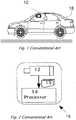
- Figure 1(conventional art) and Figure 2 (conventional art) which illustrate a system 16 including a camera or image sensor 12 mounted in a vehicle 18 imaging a field of view in the forward or rear direction.
- Image sensor 12typically delivers images in real time and the images are captured in a time series of image frames 15.
- An image processor 14is used to process image frames 15 for processing by one or more driver assistance systems.
- Driver assistance systemsinclude forward collision warning systems, lane departure warning systems, traffic sign recognition (TSR) and headlight control systems.
- TSRtraffic sign recognition
- Lane departure warning (LDW) systemsare designed to give a warning in the case of unintentional lane departure. The warning is given when the vehicle crosses or is about to cross the lane marker. Driver intention is determined based on use of turn signals, change in steering wheel angle, vehicle speed and brake activation. There are various LDW systems available.
- One algorithm for lane departure warning (LDW) used by the assignee/applicant of the present application(Mobileye Technologies Ltd., Nicosia, Cyprus, hereinafter "Mobileye”) is predictive in that it computes time to lane crossing (TLC) based on change in wheel-to-lane distance and warns when the time-to-lane crossing (TLC) is below a certain threshold.
- lane marker detection algorithmessential to the lane departure warning system is the lane marker detection algorithm.
- the lane markersare detected in the camera image and then, given the known camera geometry and camera location relative to the vehicle, the position of the vehicle relative to the lane is computed.
- the lane markers detected in the camera imageare then collected over time, for instance using a Kalman filter.
- Wheel-to-lane marker distancemay be given with an accuracy of better than 5 centimeters. With a forward looking camera, wheel-to-lane marker distance is not observed directly but is extrapolated from the forward view of the camera.
- lane markingsare detected at 50 meters and beyond.
- FOVhorizontal field of view
- a lane mark of width 0.1 meters at 50m distancecorresponds in the image plane to just under two pixels wide and can be detected accurately.
- the expectation from the lane departure warning systemsis greater than 99% availability when lane markings are visible.
- Expectation with 99% availabilityis particularly challenging to achieve in low light conditions when the lane markings are not freshly painted (have low contrast with the road) and the only light source is the car halogen headlights.
- the lane markingsare only visible using the higher sensitivity of the clear pixels (i.e. using a monochrome sensor or a red/clear sensor).
- HIDxenon high intensity discharge
- FCWforward collision warning
- TTCtime-to-contact/collision
- Traffic sign recognition (TSR) modulesare typically designed to detect speed limit signs and end-of-speed limit signs on highways, country roads and urban settings.
- iconic supplemental signse.g. rain, on exit (arrow), trailer
- TSRTraffic sign recognition
- Systems implementing traffic sign recognition (TSR)may or should ignore the following signs: signs on truck/buses, exit road numbers, minimum speed signs, and embedded signs.
- a traffic sign recognition (TSR) modulewhich focuses on speed limit signs does not have a specific detection range requirement because speed limit signs only need to be detected before they leave the image.
- An example of a difficult traffic sign to detectis a 0.8 meter diameter traffic sign on the side of the road when the vehicle is driving in the center lane of a three lane highway. Further details of a TSR system is disclosed by the present assignee in United States patent publication number US 2008/0137908 (application serial number 11/951,405 ).
- a typical automatic headlight or high/low beam control (AHC) systemdetects the following conditions and switches from high beams to low beams: headlights of oncoming vehicles, taillights of preceding vehicles, street lights or ambient light indicating that high beams are not required and a low vehicle speed. The host vehicle lights are switched back to high beams when none of these conditions exists (often after a specified given or grace period).
- One approach for detecting taillightsis to compare images from two sensors: one with a red filter and the second with a cyan filter. The cyan filter responds to non-red light sources and will give zero response to red light. By comparing corresponding pixels from two imaging sensors one can detect the color of the light source. The number of pixels of each color above a certain intensity is counted and if the count is above a threshold the systems switches to low beams.
- the use of color filters with imaging sensorsmay preclude the simultaneous use of the same image frames for other driver assistance applications.
- a second approach for automatic high-beam controluses an RGB sensor to give better color differentiation.
- Typical light sourcescan be located in the full CIE color space as defined by the International Commission on Illumination. This approach distinguishes between green, yellow and red lights. A powerful green traffic light is not confused with an oncoming vehicle.
- a single sensor with a color mosaic filter i.e. Bayer pattern mosaicis used, the lens is defocused so as to spread a light source over multiple pixels.
- the use of the color mosaic filterreduces both the effective image sensor resolution (by 50%) and the intensity response (to less than one third).
- the color mosaic filtermay preclude the use of the same sensor for traffic sign recognition (TSR) or lane departure warning (LDW) because of the intensity response penalty.
- FCWforward collision warning
- TSRtraffic sign recognition
- LWDlane departure warning
- AHCautomatic high-beam control
- the automatic high-beam control (AHC) algorithmincludes the following features: detect bright spots in the sub-sampled long exposure image and then perform clustering and classification in the full resolution image; classify spots based on brightness, edge shape, internal texture; get further brightness information from the short exposure frames, and classify obvious oncoming headlights based on size and brightness; track spots over time and compute change in size and brightness; pair up matching spots based on similarity of shape, brightness and motion; classify pairs as oncoming or taillights based on distance, brightness and color; and estimate distance and where unmatched spots might be motorcycles taillights.
- US patent US 8,254,635 B2describes "bundling" or parallel processing of multiple driver assistance systems (e.g . automatic high-beam control (AHC) and traffic sign recognition (TSR), lane departure warning (LDW), forward collision warning (FCW)) on a single hardware platform 16 , e.g. camera 12 and processor 14 .
- Bundlingprovides cost reduction and may allow more driver assistance functions to be added to the vehicle without increasing the space required beyond the windshield of the vehicle.
- driver assistance applicationshave different requirements from camera 12 , and associated optics.
- AHCautomatic high-beam control
- lane detection and traffic sign recognitionrequire the extra sensitivity of a monochrome sensor for operation under low light conditions.
- No single gain/exposure settingis optimal for all applications and in fact, some applications (such as AHC and TSR) may each use more than one gain/exposure setting.
- Most driver assistance applicationsrequire processing over multiple windows of a single frame and/or multiple image frames. In some cases, image frames are partitioned between different driver assistance applications and in other cases the image frames are shared between the different driver assistance applications.
- a vector processoror array processor, is a processor that implements an instruction set containing instructions that operate on one-dimensional arrays of data called vectors.
- a scalar processorin comparison, operates on a single datum. Most commonly used processors are scalar processors.
- VLIWVery Long Instruction Word
- VLIWVery Long Instruction Word
- the VLIWcontains multiple opcodes which direct the various sub-processing units, thus allowing for parallel processing since each sub-unit gets its opcode at the same time.
- An op-codeis a portion of a machine language instruction that specifies an operation to be performed.
- Image processing system 30has a processor 304 connected to a register 306 via a register bus 322 .
- a memory 302is connected to image sensor 12 (not shown in Fig. 3 ) for inputting one image frame 15 at a time via an image frame bus 310 .
- Processor 304has multiple arithmetic and logic units (ALU) 320 and a load store unit LSU 318 connected to a very long instruction word (VLIW) 316 via data bus 314 .
- ALU 320 and a load store unit LSU 318are connected to register 306 by register bus 322 .
- LSU 318connects to and accesses memory 302 via memory bus 312 .
- VLIW 316During operation of image processing system 30 , multiple arithmetic and logic units ALU 320 operate in parallel via op-codes (operation codes) provided by VLIW 316 . In the case of VLIW 316 , many op-codes provide multiple commands which allow parallel processing by sub-processing units ALU 320 . VLIW 316 contains address information to be used by one of ALU 320 to compute the upcoming address to be then used by LSU 318 in a subsequent cycle.
- Load-storage unit(LSU 318 ) is responsible for accessing memory 302 .
- the address for LSU 318generally comes from register file 306 where the address is the result of a computation performed by the other sub-units. As a result, LSU 318 must wait until the necessary address is calculated. Furthermore, ALU 320 requires at least one cycle to performing the address calculation instead of performing an algorithm specific computation.
- WO-2008/050256discloses an address calculation unit for region based image processing tasks, where a processing unit processes the data and exchanges the processed data between a global memory and a local memory, wherein the address calculation of region-based algorithms is performed by the address calculation unit in parallel to the date processing of the and the actual processing of data.
- MATHEW B ET AL"A loop accelerator for low power embedded VLIW processors", HARDWARE/SOFTWARE CODESIGN AND SYSTEM SYNTHESIS, INTERNATIONAL CONFERENCE ON. STOCKHOLM, SWEDEN SEPT. 8-10, 2004, IEEE, 8 September 2004, pages 6-11 , discloses a distributed address generation and loop acceleration architecture for VLIW processors is presented.
- This decentralized on-chip memory architectureuses multiple SRAMs to provide high intra-processor bandwidth.
- Each SRAMhas an associated stream address generator capable of implementing a variety of addressing modes in conjunction with a shared loop accelerator.
- image sensorrefers to or includes a photosensitive surface.
- a typical “image sensor”is electronic with a finite number of picture elements or pixels which cover an area.
- the “picture elements”typically have a length and width in image space.
- image size parameterin the context of the present invention refers to the size of an image either in image coordinates or as accessed in memory.
- image parameterrefers to one or more of the image frames as stored in memory and specifies which image frame(s) to process.
- windowrefers to a locus of pixels or a number of contiguous pixels in an image frame.
- an image processing systemincluding a vector processor and a memory adapted for attaching to the vector processor.
- the memoryis adapted to store multiple image frames.
- the vector processorincludes an address generator operatively attached to the memory to access the memory.
- the address generatoris adapted for calculating addresses of the memory over the multiple image frames.
- the addressesmay be calculated over the image frames based upon an image parameter.
- the image parametermay specify which of the image frames are processed simultaneously.
- a scalar processormay be attached to the vector processor.
- the scalar processorprovides the image parameter(s) to the address generator for address calculation over the multiple image frames.
- An input registermay be attached to the vector processor.
- the vector processormay include hardware to support looping code during execution, where the address generator is previously programmed with parameters of an execution loop over the image frames.
- the address generatormay be configured to generate a break signal adapted to be received by the hardware to break execution of the looping code of the vector processor over the image frames.
- the image framesmay be processed in parallel for multiple driver assistance applications using a single hardware platform.
- the input registermay be adapted to receive a very long instruction word (VLIW) instruction.
- the VLIW instructionmay be configured to transfer only: (i) operation codes for image processing calculations over the image frames by the ALU units and (ii) a single bit to the address generator.
- the addressesare calculated over the multiple image frames based upon at most one image size parameter which specifies a dimension of the image frames or the addresses are calculated over the multiple image frames based upon at most two image size parameters which specify a dimension of the image frames.
- a method for processing images in a systemincluding a vector processor and a memory.
- the vector processorincludes an address generator attached to the memory to access the memory.
- the address generatoris adapted for calculating addresses of the memory.
- the multiple image framesare stored in the memory.
- a VLIW instructionmay be received for the parallel processing of data stored at the calculated addresses.
- the parallel processingmay be performed by the vector processor according to the VLIW instruction.
- An image parametermay be loaded and read by the address generator. The loading of the image parameter may be performed externally to the VLIW instruction and the address generator receives only a single bit of the VLIW instruction to enable the calculation of addresses.
- the addresses of the memorymay be calculated for the image frames based upon the image parameter; and the image frames are processed in parallel using the addresses.
- the image framesare typically stored contiguously in memory.
- the loading of the image parametermay be performed in a register attached to or resident in the address generator.
- the image parametermay specify at least two of the image frames to be processed in parallel.
- the calculationis based upon the image parameter including at most two image size parameters which specify the size of the image frames.
- the calculationmay be based upon the image parameter including at most one image size parameter which specifies the size of the image frames.
- a method for processing images in a systemincluding a vector processor and a memory.
- the vector processorincludes an address generator operatively attached to the memory to access the memory.
- the vector processormay include hardware to support looping code during execution.
- the address generatoris adapted for calculating addresses of the memory.
- An image frameis stored in the memory.
- a window parameteris loaded and read which specifies multiple windows within the image frame. Addresses are calculated for the multiple windows within the image frame based upon the image parameter. Image data stored at the addresses are processed in parallel.
- the address generatormay be previously programmed with parameters of an execution loop over the image frames. Based on the previous programming, a break signal may be generated.
- the hardwaremay receive the break signal, thereby breaking execution of the looping code of the vector processor over the image frames.
- a VLIW instructionmay be received for the parallel processing of data stored at the calculated addresses.
- the parallel processingmay performed by the vector processor according to the VLIW instruction.
- the loading of the window parameteris performed externally to the VLIW instruction.
- the address generatorreceives a single bit of the VLIW instruction to enable the calculation of addresses.
- embodiments of the present inventiontake advantage of the fact that image processing is being performed involving image patches of a given width and height located in a given memory. Having specific parameters known in advance of the computation-intensive image processing allows avoiding address calculations during actual image processing.
- VLIW 316contains address information to be used by ALU 320 to compute the upcoming address to be then used by the LSU 318 in a subsequent cycle. According to an embodiment of the present invention addresses are calculated as needed, and thus VLIW bits used to pass the addressing information in conventional circuitry 30 are now available for other operand information, or simply a more compact instruction word (which thus saves on program memory used to store the instructions).
- addressing parameterse.g. width(w), height(h) in image space and origin or starting point in memory are provided and used to calculate memory addresses for multiple image frames and/or multiple windows thereby freeing up other computation sub-units for actual image processing calculations, e.g. for driver control applications.
- embodiments of the present inventionare useful for many different image processing algorithms, particularly image processing calculations and/or algorithms (including but not limited by) sum of squared differences, sum of absolute differences, median filter, Hough transform, image intensity accumulation) which process every pixel within a given image windows.
- Image processing system 40includes a vector processor 404, a memory 402 and a scalar processor 418.
- Memory 402connects to an input of multiple image frames 15 via an image frame bus 410.
- Vector processor 404includes multiple arithmetic logic units (ALU) 420 and an address generator 408 which connect to register 406 via their own separate buses (thus allowing simultaneous register file access).
- Address generator 408connects to memory 402 with a memory bus 431.
- ALUarithmetic logic units
- Arithmetic logic units (ALU) 420 and address generator 408connect to a very long instruction word (VLIW) 422 via their own separate buses (thus allowing simultaneous execution of the relevant op-codes.
- VLIWvery long instruction word
- a single bit 1b of VLIW 422connects directly to address generator 408.
- FIG. 6ashows schematically an image frame 60 in memory 402 with a window 62 according to different embodiments of the present invention.
- Window 62defines an area of interest within image frame 60.
- Image frame 60is typically larger than window 62.
- Image frame 60has pixel values which are stored in a base address.
- widthmay be defined as a difference between window 62 and the larger image frame 60 (stride is greater than width).
- the differenceis relative to the horizontal and vertical pixel co-ordinates of image frame 60 compared to window 62.
- the differencemay be calculated each time window 62 is moved around inside image frame 60.
- Window 62is traversed vertically and horizontally according to the values of ystepl ystart / ycount and xstep / xstart / xcount respectively.
- address generator 408may iteratively map image coordinates X, Y of one or more image frames into memory addresses, according to an embodiment of the present invention.
- Next AddressBase + X + Y * Width .
- Xis a pixel number per row related to a horizontal coordinate in image coordinates of an image frame.
- Yis the number of rows related to a vertical coordinate in image coordinates of the image frame.
- Widthis the number of memory addresses storing a row in an image frame or the difference between the respective first addresses storing consecutive rows.
- Baseis a pointer or memory address in memory 402 for the first memory address for one or more image frames in memory 402.
- the value of the Base pointeris a constant term added to all addresses generated through the iterations of X and Y. Multiple values of Base allow for generation of addresses for multiple image frames stored in memory 402.
- FIG. 5illustrates a flow diagram of a method 50 using image processing system 40 according to an exemplary embodiment of the present invention.
- Multiple image frames 15are stored (step 500 ) typically contiguously in memory 402 via image frame bus 410. At least two of stored multiple image frames 15 are to be processed simultaneously and/or in parallel.
- Address parametersare loaded (step 502 ) by a load storage unit of scalar processor 418 in a dedicated register of address generator 408 or in register 406.
- Address generator 408reads (step 503 ) the address parameters.
- VLIWis processed (step 501 )
- One or more of the address parameterstypically specifies the multiple image frames to be processed in parallel.
- address generator 408calculates (step 504 ) addresses required by scalar processor 418 over the multiple image frames. Otherwise, in decision block 505, address generator 408 waits for bit 1b to turn on.
- Processor 404performs image processing on the multiple image frames 15 simultaneously (step 506 ) without frame-by-frame calculation of addresses because the required addresses for the multiple image frames have been previously calculated by address generator 408 for all the multiple frames to be processed (step 506 ).
- Calculation (step 504 ) of addressesmay be performed while image frames 15 are being stored (step 502 ) in memory.
- bit 1b of VLIWis typically turned off.
- processor 404has completed processing the calculated addresses for only respective portions of all the image frames to be processed and the processing over entire image frames is not finished (decision block 507 )
- bit 1b of VLIWis typically turned on and process 50 feeds back to step 504 during which address generator 408 calculates the next portions of addresses of the multiple image frames using the same image parameters already loaded in step 502.
- address generator 408calculates the next portions of addresses of the multiple image frames using the same image parameters already loaded in step 502.
- process 50may continue with loading (step 502 ) new image parameters.
- FIG. 6billustrates a flow chart of another method using image processing system 40, according to an exemplary embodiment of the present invention.
- An image frame 15is stored (step 600 ).
- Register 406 or a dedicated register in address generator 408is loaded (step 602 ) with window parameters specifying multiple windows by scalar processor 418.
- Address generator 408reads (step 604 ) the window parameters loaded in step 602.
- VLIWis processed (step 501 ).
- bit 1b of VLIWis typically turned off.
- processor 404has completed processing the calculated addresses for only respective portions of all the windows to be processed and the processing over entire windows is not finished (decision block 607 )
- bit 1b of VLIWis typically turned on and process 60 feeds back to step 606 during which address generator 408 calculates the next portions of addresses of the multiple windows using the same image parameters already loaded in step 602.
- address generator 408calculates the next portions of addresses of the multiple windows using the same image parameters already loaded in step 602.
- process 60may continue with loading (step 602 ) new image parameters.
- Address generator 408calculates (step 606 ) the addresses of the multiple windows required by scalar processor 418.
- Vector processor 404performs image processing on the multiple windows simultaneously (step 608 ) without calculating addresses window-by-window because the addresses for multiple windows required have been previously calculated by address generator 408.
- FIG. 7illustrates a simplified block diagram of address generator 408 which calculates addresses according to Equation 1 above.
- XStartis the first value of X, which is then incremented XCount times by the value of XStep.
- Xis set to XStart each time a new X iteration is started.
- XStepis the value by which X is incremented at each X iteration, thus allowing accesses to skip over pixels.
- XCountis the number of iterations in the X image coordinate, i.e. X is incremented XCount times as determined by comparator 74X.
- YStartis the first value of Y, which is then incremented YCount times by the value of YStep.
- Yis set to YStart each time a new Y iteration is started.
- YStepis the value by which Y is incremented at each Y iteration, thus allowing accesses to skip over rows of pixels.
- YCountis the number of iterations in the Y image coordinate, i.e. Y is incremented_ YCount times as determined by comparator 74Y.
- the product as output of multiplier 76is added to X by an adder 78.
- the next address NextAddr calculatedis found by adding the base address Base to the sum from adder 78.
- equation 1may still be used by having the Base value employ an image number N i multiplied by the memory size S m .
- Bas e iN i * S m
- Base iis used to reach the start of every desired frame, which is then traversed according to equation 1.
- the feature for generating addresses over multiple image framesmay be referred to herein as generating addresses over a third dimension or a z- dimension.
- Address generator unit 408may be designed to provide addresses required by scalar processor 418 based on the image parameters loaded. For a given image, address generator 408 cycles through the x,y,z dimensions and an instruction sequence programmed for the specific coordinate is executed.
- the following operationis performed. For corresponding pixels in two distinct image frames, the intensity value of the pixels are subtracted and the result is stored.
- This operationrequires two loads, one subtract, and one store (four operations in total).
- the operationsare executed in pipeline and parallel fashion such that it takes four cycles until the store is executed, subsequently, however, a new result is stored every cycle.
- a registeris provided in register block 406 to indicate to address generator 408 not to execute the store until a delay has been met.
- address generator 408Another salient feature of address generator 408 is the ability to efficiently handle non-aligned data.
- pixel datais stored in memory that is not 8-bits wide, but rather has a bus width of 32 or 64 bits.
- VLIWVery long instruction word
- DSPdigital signal processing units
- the desired image patchis not aligned to the system bus width.
- Address generator 408includes or accesses two programmable registers which may be used to determine where the valid pixel boundaries are within the initial and final memory words of a given row.
- address generator 408may zero out the invalid data bits which allows the ALUs 420 to process the entire memory word without any influence to the calculation results. (In general, zero data does not influence algorithms involving addition and multiplication, except in special cases for which software would then have to take this into account). For memory writes, the address generator 408 may disable the Byte Enable lines corresponding to the invalid bytes.
- system 40includes hardware to support looping code thereby eliminating overhead associated with supporting loops.
- the systemcontains registers (for instance in register block 406 ) which point to the beginning of a loop and the end of the loop such that once the loop has been entered it will continuously execute autonomously forever (i.e., going from beginning to end and back to the beginning without intervention).
- registersfor instance in register block 406
- the circuitryaccepts an external "break" signal generated from address generator 408 which has been preprogrammed with the parameters of the loop (e.g., x,y max). In this way, processor resources are not wasted on handling the loop flow control.
Landscapes
- Physics & Mathematics (AREA)
- General Physics & Mathematics (AREA)
- Engineering & Computer Science (AREA)
- Theoretical Computer Science (AREA)
- Image Processing (AREA)
Description
- The present invention relates to an image processing system and specifically to an address generator used to calculate addresses so that multiple image frames or windows are processed in parallel.
- Reference is made to
Figure 1 (conventional art) andFigure 2 (conventional art) which illustrate asystem 16 including a camera orimage sensor 12 mounted in avehicle 18 imaging a field of view in the forward or rear direction.Image sensor 12 typically delivers images in real time and the images are captured in a time series ofimage frames 15. Animage processor 14 is used to processimage frames 15 for processing by one or more driver assistance systems. - Driver assistance systems include forward collision warning systems, lane departure warning systems, traffic sign recognition (TSR) and headlight control systems.
- Lane departure warning (LDW) systems are designed to give a warning in the case of unintentional lane departure. The warning is given when the vehicle crosses or is about to cross the lane marker. Driver intention is determined based on use of turn signals, change in steering wheel angle, vehicle speed and brake activation. There are various LDW systems available. One algorithm for lane departure warning (LDW) used by the assignee/applicant of the present application (Mobileye Technologies Ltd., Nicosia, Cyprus, hereinafter "Mobileye") is predictive in that it computes time to lane crossing (TLC) based on change in wheel-to-lane distance and warns when the time-to-lane crossing (TLC) is below a certain threshold. Other algorithms give a warning if the wheel is inside a certain zone around the lane marker. In either case, essential to the lane departure warning system is the lane marker detection algorithm. Typically, the lane markers are detected in the camera image and then, given the known camera geometry and camera location relative to the vehicle, the position of the vehicle relative to the lane is computed. The lane markers detected in the camera image are then collected over time, for instance using a Kalman filter. Wheel-to-lane marker distance may be given with an accuracy of better than 5 centimeters. With a forward looking camera, wheel-to-lane marker distance is not observed directly but is extrapolated from the forward view of the camera. The closer road markings are observed, less extrapolation is required for determining wheel-to-lane marker distance and more accurate estimates of wheel-to-lane marker distance are achieved, especially along curves of the road. Due to the car bonnet (hood) and the location of the camera, the road is seldom visible closer than six meters in front of the wheels of the car. In some cars with longer bonnets, the road visible in front of the wheels of the car is even less. Typically the lane departure warning system of Mobileye works on sharp curves (with radius down to 125m). With a horizontal field of view (FOV) of 39 degrees of the camera, the inner lane markers are still visible on curves with a radius down to 125 meters. In order to perform correctly lane assignment on curves, lane markings are detected at 50 meters and beyond. With a horizontal field of view (FOV) of 39 degrees for the camera, a lane mark of width 0.1 meters at 50m distance corresponds in the image plane to just under two pixels wide and can be detected accurately. The expectation from the lane departure warning systems is greater than 99% availability when lane markings are visible. Expectation with 99% availability is particularly challenging to achieve in low light conditions when the lane markings are not freshly painted (have low contrast with the road) and the only light source is the car halogen headlights. In low light conditions, the lane markings are only visible using the higher sensitivity of the clear pixels (i.e. using a monochrome sensor or a red/clear sensor). With the more powerful xenon high intensity discharge (HID) headlights, it is possible to use a standard red green blue (RGB) sensor in most low light conditions.
- The core technology behind forward collision warning (FCW) systems and headway distance monitoring is vehicle detection. Assuming reliable detection of vehicles in a single image, a typical forward collision warning (FCW) system requires that a vehicle image be 13 pixels wide, then for a car of width 1.6m, a typical camera gives initial detection at 115m and multi-frame approval at 100m. A narrower
horizontal field of view (FOV) for the camera gives a greater detection range. However, the narrower horizontal field of view (FOV) will reduce the ability to detect passing and cutting-in vehicles. A horizontal field of view (FOV) of around 40 degrees was found by Mobileye to be almost optimal (in road tests conducted with a camera) given the image sensor resolution and dimensions. A key component of a typical forward collision warning (FCW) algorithm is the estimation of distance from a single camera and the estimation of scale change from the time-to-contact/collision (TTC) as disclosed for example inUS patent 7,113,867 . - Traffic sign recognition (TSR) modules are typically designed to detect speed limit signs and end-of-speed limit signs on highways, country roads and urban settings. In addition, iconic supplemental signs (e.g. rain, on exit (arrow), trailer) are typically detected and identified. Partially occluded, slightly twisted and rotated traffic signs are preferably detected. Systems implementing traffic sign recognition (TSR) may or should ignore the following signs: signs on truck/buses, exit road numbers, minimum speed signs, and embedded signs. A traffic sign recognition (TSR) module which focuses on speed limit signs does not have a specific detection range requirement because speed limit signs only need to be detected before they leave the image. An example of a difficult traffic sign to detect is a 0.8 meter diameter traffic sign on the side of the road when the vehicle is driving in the center lane of a three lane highway. Further details of a TSR system is disclosed by the present assignee in United States patent publication number
US 2008/0137908 (application serial number11/951,405 - A typical automatic headlight or high/low beam control (AHC) system detects the following conditions and switches from high beams to low beams: headlights of oncoming vehicles, taillights of preceding vehicles, street lights or ambient light indicating that high beams are not required and a low vehicle speed. The host vehicle lights are switched back to high beams when none of these conditions exists (often after a specified given or grace period). One approach for detecting taillights is to compare images from two sensors: one with a red filter and the second with a cyan filter. The cyan filter responds to non-red light sources and will give zero response to red light. By comparing corresponding pixels from two imaging sensors one can detect the color of the light source. The number of pixels of each color above a certain intensity is counted and if the count is above a threshold the systems switches to low beams. The use of color filters with imaging sensors may preclude the simultaneous use of the same image frames for other driver assistance applications.
- A second approach for automatic high-beam control (AHC) uses an RGB sensor to give better color differentiation. Typical light sources can be located in the full CIE color space as defined by the International Commission on Illumination. This approach distinguishes between green, yellow and red lights. A powerful green traffic light is not confused with an oncoming vehicle. Since a single sensor with a color mosaic filter i.e. Bayer pattern mosaic is used, the lens is defocused so as to spread a light source over multiple pixels. The use of the color mosaic filter reduces both the effective image sensor resolution (by 50%) and the intensity response (to less than one third). The color mosaic filter may preclude the use of the same sensor for traffic sign recognition (TSR) or lane departure warning (LDW) because of the intensity response penalty.
- Given that forward collision warning (FCW), traffic sign recognition (TSR) and lane departure warning (LDW) already require a high resolution monochrome sensor, a new automatic high-beam control (AHC) algorithm was developed for use with high resolution monochrome sensors as disclosed in
US patent 7,566,851 . A number of different pattern recognition techniques are used with higher resolution monochrome imaging sensors to identify light sources instead of relying on color information. The automatic high-beam control (AHC) algorithm includes the following features: detect bright spots in the sub-sampled long exposure image and then perform clustering and classification in the full resolution image; classify spots based on brightness, edge shape, internal texture; get further brightness information from the short exposure frames, and classify obvious oncoming headlights based on size and brightness; track spots over time and compute change in size and brightness; pair up matching spots based on similarity of shape, brightness and motion; classify pairs as oncoming or taillights based on distance, brightness and color; and estimate distance and where unmatched spots might be motorcycles taillights. - US patent
US 8,254,635 B2 describes "bundling" or parallel processing of multiple driver assistance systems (e.g. automatic high-beam control (AHC) and traffic sign recognition (TSR), lane departure warning (LDW), forward collision warning (FCW)) on asingle hardware platform 16,e.g. camera 12 andprocessor 14. Bundling provides cost reduction and may allow more driver assistance functions to be added to the vehicle without increasing the space required beyond the windshield of the vehicle. - Different driver assistance applications have different requirements from
camera 12, and associated optics. For example, a conventional automatic high-beam control (AHC) algorithm makes significant use of color information and thus requires a color sensor, while lane detection and traffic sign recognition require the extra sensitivity of a monochrome sensor for operation under low light conditions. No single gain/exposure setting is optimal for all applications and in fact, some applications (such as AHC and TSR) may each use more than one gain/exposure setting. Most driver assistance applications require processing over multiple windows of a single frame and/or multiple image frames. In some cases, image frames are partitioned between different driver assistance applications and in other cases the image frames are shared between the different driver assistance applications. - A vector processor, or array processor, is a processor that implements an instruction set containing instructions that operate on one-dimensional arrays of data called vectors. A scalar processor, in comparison, operates on a single datum. Most commonly used processors are scalar processors.
- VLIW (Very Long Instruction Word) digital signal processing units contain several sub-processing units which operate in parallel. The VLIW contains multiple opcodes which direct the various sub-processing units, thus allowing for parallel processing since each sub-unit gets its opcode at the same time. An op-code is a portion of a machine language instruction that specifies an operation to be performed.
- Reference is now made to
Figure 3 , a system block diagram for a conventionalimage processing system 30.Image processing system 30 has aprocessor 304 connected to aregister 306 via aregister bus 322. Amemory 302 is connected to image sensor12 (not shown inFig. 3 ) for inputting oneimage frame 15 at a time via animage frame bus 310.Processor 304 has multiple arithmetic and logic units (ALU)320 and a loadstore unit LSU 318 connected to a very long instruction word (VLIW)316 viadata bus 314.ALU 320 and a loadstore unit LSU 318 are connected to register306 byregister bus 322.LSU 318 connects to and accessesmemory 302 viamemory bus 312. - During operation of
image processing system 30, multiple arithmetic andlogic units ALU 320 operate in parallel via op-codes (operation codes) provided byVLIW 316. In the case ofVLIW 316, many op-codes provide multiple commands which allow parallel processing bysub-processing units ALU 320.VLIW 316 contains address information to be used by one ofALU 320 to compute the upcoming address to be then used byLSU 318 in a subsequent cycle. - Load-storage unit (LSU318) is responsible for accessing
memory 302. The address forLSU 318 generally comes fromregister file 306 where the address is the result of a computation performed by the other sub-units. As a result,LSU 318 must wait until the necessary address is calculated. Furthermore,ALU 320 requires at least one cycle to performing the address calculation instead of performing an algorithm specific computation. - Thus there is a need for and it would be advantageous to have a hardware platform suitable to support multiple image frames and/or multiple windows for processing in parallel multiple driver assistance applications, and specifically the preferred embodiments described herein provide an address generator which calculates addresses over multiple image frames and/or multiple windows to support processing of multiple driver assistance applications using a single hardware platform.
WO-2008/050256 discloses an address calculation unit for region based image processing tasks, where a processing unit processes the data and exchanges the processed data between a global memory and a local memory, wherein the address calculation of region-based algorithms is performed by the address calculation unit in parallel to the date processing of the and the actual processing of data. - MATHEW B ET AL: "A loop accelerator for low power embedded VLIW processors", HARDWARE/SOFTWARE CODESIGN AND SYSTEM SYNTHESIS, INTERNATIONAL CONFERENCE ON. STOCKHOLM, SWEDEN SEPT. 8-10, 2004, IEEE, 8 September 2004, pages 6-11, discloses a distributed address generation and loop acceleration architecture for VLIW processors is presented. This decentralized on-chip memory architecture uses multiple SRAMs to provide high intra-processor bandwidth. Each SRAM has an associated stream address generator capable of implementing a variety of addressing modes in conjunction with a shared loop accelerator.
- The term "image sensor" as used herein refers to or includes a photosensitive surface. A typical "image sensor" is electronic with a finite number of picture elements or pixels which cover an area. The "picture elements" typically have a length and width in image space.
- The term "image size parameter" in the context of the present invention refers to the size of an image either in image coordinates or as accessed in memory.
- The term "image parameter" refers to one or more of the image frames as stored in memory and specifies which image frame(s) to process. The term "window" as used herein refers to a locus of pixels or a number of contiguous pixels in an image frame.
- The terms "parameter", "address parameter" or "addressing parameter" are used herein interchangeably and refer to both said "image size parameter" and "image parameter".
- According to a feature of the present invention there is provided an image processing system including a vector processor and a memory adapted for attaching to the vector processor. The memory is adapted to store multiple image frames. The vector processor includes an address generator operatively attached to the memory to access the memory. The address generator is adapted for calculating addresses of the memory over the multiple image frames. The addresses may be calculated over the image frames based upon an image parameter. The image parameter may specify which of the image frames are processed simultaneously. A scalar processor may be attached to the vector processor. The scalar processor provides the image parameter(s) to the address generator for address calculation over the multiple image frames. An input register may be attached to the vector processor. The vector processor may include hardware to support looping code during execution, where the address generator is previously programmed with parameters of an execution loop over the image frames. The address generator may be configured to generate a break signal adapted to be received by the hardware to break execution of the looping code of the vector processor over the image frames. The image frames may be processed in parallel for multiple driver assistance applications using a single hardware platform. The input register may be adapted to receive a very long instruction word (VLIW) instruction. The VLIW instruction may be configured to transfer only: (i) operation codes for image processing calculations over the image frames by the ALU units and (ii) a single bit to the address generator. The addresses are calculated over the multiple image frames based upon at most one image size parameter which specifies a dimension of the image frames or the addresses are calculated over the multiple image frames based upon at most two image size parameters which specify a dimension of the image frames.
- According to a feature of the present invention there is provided a method for processing images in a system including a vector processor and a memory. The vector processor includes an address generator attached to the memory to access the memory. The address generator is adapted for calculating addresses of the memory. The multiple image frames are stored in the memory. A VLIW instruction may be received for the parallel processing of data stored at the calculated addresses. The parallel processing may be performed by the vector processor according to the VLIW instruction. An image parameter may be loaded and read by the address generator. The loading of the image parameter may be performed externally to the VLIW instruction and the address generator receives only a single bit of the VLIW instruction to enable the calculation of addresses. The addresses of the memory may be calculated for the image frames based upon the image parameter; and the image frames are processed in parallel using the addresses. The image frames are typically stored contiguously in memory. The loading of the image parameter may be performed in a register attached to or resident in the address generator. The image parameter may specify at least two of the image frames to be processed in parallel. The calculation is based upon the image parameter including at most two image size parameters which specify the size of the image frames. The calculation may be based upon the image parameter including at most one image size parameter which specifies the size of the image frames.
- According to a feature of the present invention there is provided a method for processing images in a system including a vector processor and a memory. The vector processor includes an address generator operatively attached to the memory to access the memory. The vector processor may include hardware to support looping code during execution. The address generator is adapted for calculating addresses of the memory. An image frame is stored in the memory. A window parameter is loaded and read which specifies multiple windows within the image frame. Addresses are calculated for the multiple windows within the image frame based upon the image parameter. Image data stored at the addresses are processed in parallel. The address generator may be previously programmed with parameters of an execution loop over the image frames. Based on the previous programming, a break signal may be generated. The hardware may receive the break signal, thereby breaking execution of the looping code of the vector processor over the image frames. A VLIW instruction may be received for the parallel processing of data stored at the calculated addresses. The parallel processing may performed by the vector processor according to the VLIW instruction. The loading of the window parameter is performed externally to the VLIW instruction. The address generator receives a single bit of the VLIW instruction to enable the calculation of addresses.
- These, additional, and/or other aspects and/or advantages of the present invention are set forth in the detailed description which follows; possibly inferable from the detailed description; and/or learnable by practice of the present invention.
- Embodiments of the present invention are described below, by way of example only, with reference to the accompanying drawings, in which:
Fig. 1 shows a camera mounted on a vehicle according to conventional art;Fig. 2 shows a vehicle control system according to conventional art;Fig. 3 shows a system block diagram of an image processing system according to conventional art;Fig. 4 shows a system block diagram of an image processing system and address generator connected according to an embodiment of the present invention;Fig. 5 shows a flow diagram of a method using an image processing system and address generator according to an embodiment of the present invention;Fig. 6 illustrates a method using an image processing system and address generator, according to another embodiment of the present invention;Figure 6a shows schematically a diagram of an image frame withwindow 60 according to an embodiment of the present invention; andFigure 7 illustrates a simplified block diagram of address generator according to embodiment of the present invention.- Reference will now be made in detail to embodiments of the present invention, examples of which are illustrated in the accompanying drawings, wherein like reference numerals refer to the like elements throughout. The embodiments are described below to explain the present invention by referring to the figures.
- By way of introduction, embodiments of the present invention take advantage of the fact that image processing is being performed involving image patches of a given width and height located in a given memory. Having specific parameters known in advance of the computation-intensive image processing allows avoiding address calculations during actual image processing.
- Using
conventional circuitry 30VLIW 316 contains address information to be used byALU 320 to compute the upcoming address to be then used by theLSU 318 in a subsequent cycle. According to an embodiment of the present invention addresses are calculated as needed, and thus VLIW bits used to pass the addressing information inconventional circuitry 30 are now available for other operand information, or simply a more compact instruction word (which thus saves on program memory used to store the instructions). - According to an embodiment of the present invention, addressing parameters, e.g. width(w), height(h) in image space and origin or starting point in memory are provided and used to calculate memory addresses for multiple image frames and/or multiple windows thereby freeing up other computation sub-units for actual image processing calculations, e.g. for driver control applications.
- It should be noted that embodiments of the present invention are useful for many different image processing algorithms, particularly image processing calculations and/or algorithms (including but not limited by) sum of squared differences, sum of absolute differences, median filter, Hough transform, image intensity accumulation) which process every pixel within a given image windows.
- Referring now to the drawings,
Figure 4 illustrates a system block diagram for animage processing system 40 according to an embodiment of the present invention.Image processing system 40 includes avector processor 404, amemory 402 and ascalar processor 418.Memory 402 connects to an input of multiple image frames15 via animage frame bus 410.Vector processor 404 includes multiple arithmetic logic units (ALU)420 and anaddress generator 408 which connect to register406 via their own separate buses (thus allowing simultaneous register file access).Address generator 408 connects tomemory 402 with amemory bus 431. Arithmetic logic units (ALU)420 andaddress generator 408 connect to a very long instruction word (VLIW)422 via their own separate buses (thus allowing simultaneous execution of the relevant op-codes. Asingle bit 1b ofVLIW 422 connects directly to addressgenerator 408. - Reference is now made to
Figure 6a which shows schematically animage frame 60 inmemory 402 with awindow 62 according to different embodiments of the present invention. The vertical and horizontal dimensions ofwindow 62 are defined byymax-ymin (height) andxmax-xmin (width) respectively.Window 62 defines an area of interest withinimage frame 60.Image frame 60 is typically larger thanwindow 62.Image frame 60 has pixel values which are stored in abase address. Using the parameterwidth for example;width may be defined as a difference betweenwindow 62 and the larger image frame60(stride is greater thanwidth). The difference is relative to the horizontal and vertical pixel co-ordinates ofimage frame 60 compared towindow 62. The difference may be calculated eachtime window 62 is moved around insideimage frame 60.Window 62 is traversed vertically and horizontally according to the values ofystepl ystart/ycount andxstep/xstart/xcount respectively. - By way of example only, the following equation may be used by
address generator 408 to iteratively map image coordinatesX, Y of one or more image frames into memory addresses, according to an embodiment of the present invention.
- WhereX is a pixel number per row related to a horizontal coordinate in image coordinates of an image frame.Y is the number of rows related to a vertical coordinate in image coordinates of the image frame.X, Y may be equivalently defined in terms of the memory addresses storing the image frame with certain assumptions, for instance one byte per pixel intensity datum.)Width is the number of memory addresses storing a row in an image frame or the difference between the respective first addresses storing consecutive rows.Base is a pointer or memory address in
memory 402 for the first memory address for one or more image frames inmemory 402. The value of theBase pointer is a constant term added to all addresses generated through the iterations ofX andY. Multiple values ofBase allow for generation of addresses for multiple image frames stored inmemory 402. - Reference is now also made to
Figure 5 which illustrates a flow diagram of amethod 50 usingimage processing system 40 according to an exemplary embodiment of the present invention. Multiple image frames15 are stored (step500) typically contiguously inmemory 402 viaimage frame bus 410. At least two of stored multiple image frames15 are to be processed simultaneously and/or in parallel. Address parameters are loaded (step502) by a load storage unit ofscalar processor 418 in a dedicated register ofaddress generator 408 or inregister 406.Address generator 408 reads (step503) the address parameters. VLIW is processed (step501) One or more of the address parameters typically specifies the multiple image frames to be processed in parallel. If single bit labeled1b inVLIW 422 of system40 (Figure 4 ) is on, (either "1" or "0") (decision block505), then addressgenerator 408 calculates (step504) addresses required byscalar processor 418 over the multiple image frames. Otherwise, indecision block 505,address generator 408 waits forbit 1b to turn on.Processor 404 performs image processing on the multiple image frames15 simultaneously (step506) without frame-by-frame calculation of addresses because the required addresses for the multiple image frames have been previously calculated byaddress generator 408 for all the multiple frames to be processed (step506). Calculation (step504) of addresses may be performed while image frames15 are being stored (step502) in memory. During processing (step506),bit 1b of VLIW is typically turned off. Whenprocessor 404 has completed processing the calculated addresses for only respective portions of all the image frames to be processed and the processing over entire image frames is not finished (decision block507), then bit1b of VLIW is typically turned on andprocess 50 feeds back to step504 during which addressgenerator 408 calculates the next portions of addresses of the multiple image frames using the same image parameters already loaded instep 502. When indecision box 507 processing of all the addresses of the multiple image frames is completed then process50 may continue with loading (step502) new image parameters. - Reference is now also made to
Figure 6b which illustrates a flow chart of another method usingimage processing system 40, according to an exemplary embodiment of the present invention. Animage frame 15 is stored (step600).Register 406 or a dedicated register inaddress generator 408 is loaded (step602) with window parameters specifying multiple windows byscalar processor 418.Address generator 408 reads (step604) the window parameters loaded instep 602. VLIW is processed (step501). - During processing (step606),
bit 1b of VLIW is typically turned off. Whenprocessor 404 has completed processing the calculated addresses for only respective portions of all the windows to be processed and the processing over entire windows is not finished (decision block607), then bit1b of VLIW is typically turned on andprocess 60 feeds back to step606 during which addressgenerator 408 calculates the next portions of addresses of the multiple windows using the same image parameters already loaded instep 602. When indecision box 607 processing of all the addresses in the multiple windows is completed then process60 may continue with loading (step602) new image parameters. Address generator 408 calculates (step606) the addresses of the multiple windows required byscalar processor 418.Vector processor 404 performs image processing on the multiple windows simultaneously (step608) without calculating addresses window-by-window because the addresses for multiple windows required have been previously calculated byaddress generator 408.- Reference is now made to
Figure 7 which illustrates a simplified block diagram ofaddress generator 408 which calculates addresses according toEquation 1 above. Acounter 72X is used to iterate in the horizontal direction in image coordinates,X=X+XStep. XStart is the first value of X, which is then incrementedXCount times by the value ofXStep. X is set toXStart each time a newX iteration is started.XStep is the value by whichX is incremented at eachX iteration, thus allowing accesses to skip over pixels.XCount is the number of iterations in the X image coordinate, i.e.X is incrementedXCount times as determined bycomparator 74X. - A
counter 72Y is used to iterate in the vertical direction in image coordinates,Y=Y+YStep. YStart is the first value of Y, which is then incrementedYCount times by the value ofYStep. Y is set toYStart each time a newY iteration is started.YStep is the value by whichY is incremented at eachY iteration, thus allowing accesses to skip over rows of pixels.YCount is the number of iterations in the Y image coordinate, i.e.Y is incremented_YCount times as determined bycomparator 74Y. - Multiplication of the number of memory addresses storing a row,Width, by the number of rowsY, is performed by
multiplier 76. The product as output ofmultiplier 76 is added toX by anadder 78. The next addressNextAddr calculated is found by adding the base addressBase to the sum fromadder 78. - For processing two or more image frames of the same size,
equation 1 may still be used by having theBase value employ an image numberNi multiplied by the memory sizeSm.
- Thus, Basei is used to reach the start of every desired frame, which is then traversed according to
equation 1. - Thus, the feature for generating addresses over multiple image frames may be referred to herein as generating addresses over a third dimension or a z- dimension.
Address generator unit 408 may be designed to provide addresses required byscalar processor 418 based on the image parameters loaded. For a given image,address generator 408 cycles through the x,y,z dimensions and an instruction sequence programmed for the specific coordinate is executed.- As an example the following operation is performed. For corresponding pixels in two distinct image frames, the intensity value of the pixels are subtracted and the result is stored.
- This operation requires two loads, one subtract, and one store (four operations in total). The operations are executed in pipeline and parallel fashion such that it takes four cycles until the store is executed, subsequently, however, a new result is stored every cycle. In order to account for this pipeline delay, a register is provided in
register block 406 to indicate to addressgenerator 408 not to execute the store until a delay has been met. - Another salient feature of
address generator 408 is the ability to efficiently handle non-aligned data. In a typical 8-bit pixel image processing system, pixel data is stored in memory that is not 8-bits wide, but rather has a bus width of 32 or 64 bits. (There are two reasons for using wide buses: (1) Very long instruction word (VLIW) digital signal processing units (DSP) handle multiple pairs of inputs in parallel, and thus the system should be capable of supplying multiple pixels (e.g., 8 pixels = 64bit memory accesses) to maintain the units in full operation. (2) Furthermore, by increasing the width of the system bus this correspondingly reduces the number of access cycles needed to DMA images into local memory.) Statistically, the desired image patch is not aligned to the system bus width. There are one or more "undesired" pixels in the memory word read before the first valid pixels in the first row. The same is true of the row end; the last valid memory word is read followed by a number of undesired pixels. - Thus, any processing should eliminate, ignore, or mask out the undesired pixels read in the first and last memory words of every row processed and should also ensure that invalid data is not written back to memory.
Address generator 408 includes or accesses two programmable registers which may be used to determine where the valid pixel boundaries are within the initial and final memory words of a given row. - For memory reads,
address generator 408 may zero out the invalid data bits which allows theALUs 420 to process the entire memory word without any influence to the calculation results. (In general, zero data does not influence algorithms involving addition and multiplication, except in special cases for which software would then have to take this into account). For memory writes, theaddress generator 408 may disable the Byte Enable lines corresponding to the invalid bytes. - In a standard processor there is a program counter which points to the next instruction to execute; usually the next memory location in program memory, unless there is a programmed branch instruction which then forces the program counter to the program memory location pointed to by the branch instruction. The processor loads the new address from the BRA instruction. Furthermore, the processor determines if the loop has completed. Hence conventional flow control requires computing resources and clock cycles.
- In contrast,
system 40 includes hardware to support looping code thereby eliminating overhead associated with supporting loops. The system contains registers (for instance in register block406) which point to the beginning of a loop and the end of the loop such that once the loop has been entered it will continuously execute autonomously forever (i.e., going from beginning to end and back to the beginning without intervention). In order to break the "infinite loop" the circuitry accepts an external "break" signal generated fromaddress generator 408 which has been preprogrammed with the parameters of the loop (e.g., x,y max). In this way, processor resources are not wasted on handling the loop flow control. - The definite articles "a", "an" are used herein, such as "an image parameter", "an address generator", "a register", "a processor" have the meaning of "one or more" that is "one or more image parameters", "one or more address generators " "one or more registers" or "one or more processors".
- Examples of various features/aspects/components/operations have been provided to facilitate understanding of the disclosed embodiments of the present invention. In addition, various preferences have been discussed to facilitate understanding of the disclosed embodiments of the present invention. It is to be understood that all examples and preferences disclosed herein are intended to be non-limiting.


Claims (11)
- An image processing system (40) including:a vector processor (404) that comprises multiple arithmetic logic units (420), an address generator (408) and a scalar processor (418); anda memory (402) operable for operatively attaching to said vector processor (404),
wherein said memory (402) is operable to store multiple image windows (15) to be processed in parallel;wherein the address generator (408) is operatively attached to said memory (402) to access said memory (402);wherein the image processing system (40) ischaracterized by having a register (406) adapted to store image parameters that specify the multiple image windows (15) to be processed in parallel;wherein the image processing system (40) is operable to store a very long instruction word (VLIW) instruction that includes operation codes for image processing calculations over the image windows (15) by the multiple arithmetic logic units (420);wherein said VLIW instruction is configured to transfer only: (i) operation codes for image processing calculations over said image windows (15) by at least one ALU unit (420) of the multiple arithmetic logic units (420), and (ii) a single bit (1b) to said address generator (408) to enable the calculation of addresses by said address generator (408);wherein the address generator (408) is configured to be loaded with window parameters specifying multiple windows by said scalar processor (418);wherein the vector processor (404) is operable to process in parallel the multiple image windows (15) based on the addresses of the multiple image windows (15) and based on the operation codes of the VLIW instruction. - The image processing system (40) according to claim 1 wherein the address generator (408) is operable to calculate the addresses when the single bit (1b) of said VLIW instruction is on and to wait before calculating the addresses when the single bit (1b) is off.
- The image processing system (40) according to claim 1 wherein the image parameters point to a beginning of an execution loop and to the end of the execution loop; wherein the vector processor (404) includes hardware to support looping code during execution of the execution loop, and based on a region of interest in said image windows (15), said address generator (408) is configured to generate a break signal to be received by said hardware to break the execution of said looping code of the vector processor (404) over the image windows (15).
- The image processing system (40) according to any preceding claim, wherein said addresses are calculated over said multiple image windows (15) based upon at most one image size parameter which specifies a dimension of said image windows (15).
- The image processing system (40) according to any of claims 1 to 3, wherein said addresses are calculated over said multiple image windows (15) based upon at most two image size parameters which specify a dimension of said image windows (15).
- A method of processing images in a system (40) including a register (406), a vector processor (404) and a memory (402), wherein the vector processor (404) includes an address generator (408), multiple arithmetic logic units (420) and a scalar processor (418); the method including the steps of:storing multiple image windows (15) to be processed in parallel in the memory (402); andaccessing the memory (402) by the address generator (408);wherein the method ischaracterized by storing (a) image parameters that specify the multiple image windows to be processed in parallel, and (b) a very long instruction word (VLIW) instruction that includes operation codes for image processing calculations over the image windows by the multiple arithmetic logic units; wherein said VLIW instruction is configured to transfer only: (i) operation codes for image processing calculations over said image windows (15) by at least one ALU unit (420) of the multiple arithmetic logic units (420), and (ii) a single bit (1b) to said address generator to enable the calculation of addresses by said address generator (408);loading window parameters specifying multiple windows by said scalar processor (418) to said address generator (408); andprocessing in parallel and by vector processor (404), the multiple image windows based on the addresses of the multiple image windows and based on the operation codes of the VLIW instruction.
- The method according to claim 6 comprising calculating by the address generator (408) the addresses when the bit (1b) is on and waiting before calculating the addresses when the bit is off.
- The method according to claim 7, wherein the loading of said image parameters is performed externally to said VLIW instruction.
- The method according to claim 6 wherein the image parameters point to a beginning of an execution loop and to the end of the execution loop; wherein the vector processor (404) includes hardware to support looping code during execution of the execution loop, wherein the method comprises generating, based on a region of interest in said image windows (15), by the address generator (408), a break signal to be received by said hardware to break the execution of said looping code of the vector processor (404) over the image windows (15).
- The method according to any one of claims 7 to 9, wherein said calculating is based upon said parameters including at most one image size parameters which specify the size of said image windows (15).
- The method according to any one of claims 7 to 9, wherein said calculating is based upon said parameters including at most two image size parameters which specify the size of said image windows (15).
Priority Applications (1)
| Application Number | Priority Date | Filing Date | Title |
|---|---|---|---|
| EP10165686.6AEP2395472B1 (en) | 2010-06-11 | 2010-06-11 | Image processing system and address generator therefor |
Applications Claiming Priority (1)
| Application Number | Priority Date | Filing Date | Title |
|---|---|---|---|
| EP10165686.6AEP2395472B1 (en) | 2010-06-11 | 2010-06-11 | Image processing system and address generator therefor |
Publications (2)
| Publication Number | Publication Date |
|---|---|
| EP2395472A1 EP2395472A1 (en) | 2011-12-14 |
| EP2395472B1true EP2395472B1 (en) | 2019-05-01 |
Family
ID=43100920
Family Applications (1)
| Application Number | Title | Priority Date | Filing Date |
|---|---|---|---|
| EP10165686.6AActiveEP2395472B1 (en) | 2010-06-11 | 2010-06-11 | Image processing system and address generator therefor |
Country Status (1)
| Country | Link |
|---|---|
| EP (1) | EP2395472B1 (en) |
Families Citing this family (21)
| Publication number | Priority date | Publication date | Assignee | Title |
|---|---|---|---|---|
| US5877897A (en) | 1993-02-26 | 1999-03-02 | Donnelly Corporation | Automatic rearview mirror, vehicle lighting control and vehicle interior monitoring system using a photosensor array |
| US6822563B2 (en) | 1997-09-22 | 2004-11-23 | Donnelly Corporation | Vehicle imaging system with accessory control |
| US7655894B2 (en) | 1996-03-25 | 2010-02-02 | Donnelly Corporation | Vehicular image sensing system |
| ES2391556T3 (en) | 2002-05-03 | 2012-11-27 | Donnelly Corporation | Object detection system for vehicles |
| US7526103B2 (en) | 2004-04-15 | 2009-04-28 | Donnelly Corporation | Imaging system for vehicle |
| WO2008024639A2 (en) | 2006-08-11 | 2008-02-28 | Donnelly Corporation | Automatic headlamp control system |
| US10318308B2 (en) | 2012-10-31 | 2019-06-11 | Mobileye Vision Technologies Ltd. | Arithmetic logic unit |
| CA3049019A1 (en) | 2017-01-10 | 2018-07-19 | Cavh Llc | Connected automated vehicle highway systems and methods |
| US10380886B2 (en) | 2017-05-17 | 2019-08-13 | Cavh Llc | Connected automated vehicle highway systems and methods |
| WO2018132378A2 (en) | 2017-01-10 | 2018-07-19 | Cavh Llc | Connected automated vehicle highway systems and methods |
| US10692365B2 (en) | 2017-06-20 | 2020-06-23 | Cavh Llc | Intelligent road infrastructure system (IRIS): systems and methods |
| US12008893B2 (en) | 2017-05-17 | 2024-06-11 | Cavh Llc | Autonomous vehicle (AV) control system with roadside unit (RSU) network |
| US10867512B2 (en) | 2018-02-06 | 2020-12-15 | Cavh Llc | Intelligent road infrastructure system (IRIS): systems and methods |
| AU2019266266B2 (en) | 2018-05-09 | 2024-06-20 | Cavh Llc | Systems and methods for driving intelligence allocation between vehicles and highways |
| WO2019246246A1 (en) | 2018-06-20 | 2019-12-26 | Cavh Llc | Connected automated vehicle highway systems and methods related to heavy vehicles |
| US12057011B2 (en) | 2018-06-28 | 2024-08-06 | Cavh Llc | Cloud-based technology for connected and automated vehicle highway systems |
| WO2020014128A1 (en) | 2018-07-10 | 2020-01-16 | Cavh Llc | Vehicle on-board unit for connected and automated vehicle systems |
| US11373122B2 (en) | 2018-07-10 | 2022-06-28 | Cavh Llc | Fixed-route service system for CAVH systems |
| US11735041B2 (en) | 2018-07-10 | 2023-08-22 | Cavh Llc | Route-specific services for connected automated vehicle highway systems |
| CN113835420A (en) | 2020-06-23 | 2021-12-24 | 上海丰豹商务咨询有限公司 | Function distribution system for automatic driving system |
| CN114360269A (en) | 2020-10-12 | 2022-04-15 | 上海丰豹商务咨询有限公司 | Automatic driving cooperative control system and method under intelligent network connection road support |
Citations (2)
| Publication number | Priority date | Publication date | Assignee | Title |
|---|---|---|---|---|
| US4338660A (en)* | 1979-04-13 | 1982-07-06 | Relational Memory Systems, Inc. | Relational break signal generating device |
| WO2003100600A2 (en)* | 2002-05-24 | 2003-12-04 | Koninklijke Philips Electronics N.V. | An address generation unit for a processor |
Family Cites Families (5)
| Publication number | Priority date | Publication date | Assignee | Title |
|---|---|---|---|---|
| US7113867B1 (en) | 2000-11-26 | 2006-09-26 | Mobileye Technologies Limited | System and method for detecting obstacles to vehicle motion and determining time to contact therewith using sequences of images |
| US7088872B1 (en)* | 2002-02-14 | 2006-08-08 | Cogent Systems, Inc. | Method and apparatus for two dimensional image processing |
| US6735682B2 (en)* | 2002-03-28 | 2004-05-11 | Intel Corporation | Apparatus and method for address calculation |
| EP1837803A3 (en) | 2006-03-24 | 2008-05-14 | MobilEye Technologies, Ltd. | Headlight, taillight and streetlight detection |
| US20100141668A1 (en)* | 2006-10-26 | 2010-06-10 | Nxp, B.V. | Address calculation unit |
- 2010
- 2010-06-11EPEP10165686.6Apatent/EP2395472B1/enactiveActive
Patent Citations (2)
| Publication number | Priority date | Publication date | Assignee | Title |
|---|---|---|---|---|
| US4338660A (en)* | 1979-04-13 | 1982-07-06 | Relational Memory Systems, Inc. | Relational break signal generating device |
| WO2003100600A2 (en)* | 2002-05-24 | 2003-12-04 | Koninklijke Philips Electronics N.V. | An address generation unit for a processor |
Non-Patent Citations (1)
| Title |
|---|
| YAMASAKI K ET AL: "External memory bist for system-in-package", TEST, 2005 IEEE INTERNATIONAL CONFERENCE ON NOV. 8, 2005, IEEE OPERATIONS CENTER, US, 8 November 2005 (2005-11-08), pages 1145 - 1154, XP010888333* |
Also Published As
| Publication number | Publication date |
|---|---|
| EP2395472A1 (en) | 2011-12-14 |
Similar Documents
| Publication | Publication Date | Title |
|---|---|---|
| EP2395472B1 (en) | Image processing system and address generator therefor | |
| US8892853B2 (en) | Hardware to support looping code in an image processing system | |
| US11409303B2 (en) | Image processing method for autonomous driving and apparatus thereof | |
| US20230196921A1 (en) | Image generating apparatus, image generating method, and recording medium | |
| Heimberger et al. | Computer vision in automated parking systems: Design, implementation and challenges | |
| JP6866440B2 (en) | Object identification methods, devices, equipment, vehicles and media | |
| JP4321591B2 (en) | In-vehicle fog determination device | |
| US11042761B2 (en) | Method and system for sensing an obstacle, and storage medium | |
| WO2007083494A1 (en) | Graphic recognition device, graphic recognition method, and graphic recognition program | |
| US20080056537A1 (en) | Camera with Two or More Angles of View | |
| JPH05265547A (en) | On-vehicle outside monitoring device | |
| JP2015103894A (en) | On-vehicle image processing apparatus, and semiconductor device | |
| US11776277B2 (en) | Apparatus, method, and computer program for identifying state of object, and controller | |
| CN103477623A (en) | Image processing device | |
| CN118470681A (en) | Traffic light detection method and device, electronic equipment and storage medium | |
| Mandumula et al. | Multi-Sensor Object Detection System for Real-Time Inferencing in ADAS | |
| EP4303850A1 (en) | Object detection method and object detection device | |
| CN116118626A (en) | Vehicle Blind Spot Visualization Method, Device, Vehicle and Storage Medium | |
| Schewior et al. | A hardware accelerated configurable ASIP architecture for embedded real-time video-based driver assistance applications | |
| CN115439509A (en) | Multi-target tracking method and device, computer equipment and storage medium | |
| JP2013172378A (en) | Image processing device and vehicle | |
| KR102019594B1 (en) | Vehicle to vehicle distance estimation method using compensation technique for low resolution camera and apparatus thereof | |
| US20230297497A1 (en) | Evaluating a floating-point accuracy of a compiler | |
| Sakurai et al. | Overtaking vehicle detection method and its implementation using IMAPCAR highly parallel image processor | |
| Rattei et al. | Shadow-based vehicle model refinement and tracking in advanced automotive driver assistance systems |
Legal Events
| Date | Code | Title | Description |
|---|---|---|---|
| AK | Designated contracting states | Kind code of ref document:A1 Designated state(s):AL AT BE BG CH CY CZ DE DK EE ES FI FR GB GR HR HU IE IS IT LI LT LU LV MC MK MT NL NO PL PT RO SE SI SK SM TR | |
| AX | Request for extension of the european patent | Extension state:BA ME RS | |
| PUAI | Public reference made under article 153(3) epc to a published international application that has entered the european phase | Free format text:ORIGINAL CODE: 0009012 | |
| 17P | Request for examination filed | Effective date:20120604 | |
| 17Q | First examination report despatched | Effective date:20120914 | |
| RAP1 | Party data changed (applicant data changed or rights of an application transferred) | Owner name:MOBILEYE VISION TECHNOLOGIES LTD. | |
| STAA | Information on the status of an ep patent application or granted ep patent | Free format text:STATUS: EXAMINATION IS IN PROGRESS | |
| GRAP | Despatch of communication of intention to grant a patent | Free format text:ORIGINAL CODE: EPIDOSNIGR1 | |
| STAA | Information on the status of an ep patent application or granted ep patent | Free format text:STATUS: GRANT OF PATENT IS INTENDED | |
| INTG | Intention to grant announced | Effective date:20180801 | |
| RIN1 | Information on inventor provided before grant (corrected) | Inventor name:DOGON, GIL Inventor name:NAVON, MOIS Inventor name:SAJMAN, ROMAN Inventor name:ARBELI, YOSI Inventor name:KREININ, YOSEF Inventor name:SIXSOU, EMMANUEL | |
| GRAJ | Information related to disapproval of communication of intention to grant by the applicant or resumption of examination proceedings by the epo deleted | Free format text:ORIGINAL CODE: EPIDOSDIGR1 | |
| STAA | Information on the status of an ep patent application or granted ep patent | Free format text:STATUS: EXAMINATION IS IN PROGRESS | |
| GRAP | Despatch of communication of intention to grant a patent | Free format text:ORIGINAL CODE: EPIDOSNIGR1 | |
| INTC | Intention to grant announced (deleted) | ||
| STAA | Information on the status of an ep patent application or granted ep patent | Free format text:STATUS: GRANT OF PATENT IS INTENDED | |
| INTG | Intention to grant announced | Effective date:20190103 | |
| GRAS | Grant fee paid | Free format text:ORIGINAL CODE: EPIDOSNIGR3 | |
| GRAA | (expected) grant | Free format text:ORIGINAL CODE: 0009210 | |
| STAA | Information on the status of an ep patent application or granted ep patent | Free format text:STATUS: THE PATENT HAS BEEN GRANTED | |
| AK | Designated contracting states | Kind code of ref document:B1 Designated state(s):AL AT BE BG CH CY CZ DE DK EE ES FI FR GB GR HR HU IE IS IT LI LT LU LV MC MK MT NL NO PL PT RO SE SI SK SM TR | |
| REG | Reference to a national code | Ref country code:GB Ref legal event code:FG4D | |
| REG | Reference to a national code | Ref country code:CH Ref legal event code:EP Ref country code:AT Ref legal event code:REF Ref document number:1127920 Country of ref document:AT Kind code of ref document:T Effective date:20190515 | |
| REG | Reference to a national code | Ref country code:DE Ref legal event code:R096 Ref document number:602010058524 Country of ref document:DE | |
| REG | Reference to a national code | Ref country code:IE Ref legal event code:FG4D | |
| REG | Reference to a national code | Ref country code:NL Ref legal event code:MP Effective date:20190501 | |
| REG | Reference to a national code | Ref country code:LT Ref legal event code:MG4D | |
| PG25 | Lapsed in a contracting state [announced via postgrant information from national office to epo] | Ref country code:NO Free format text:LAPSE BECAUSE OF FAILURE TO SUBMIT A TRANSLATION OF THE DESCRIPTION OR TO PAY THE FEE WITHIN THE PRESCRIBED TIME-LIMIT Effective date:20190801 Ref country code:LT Free format text:LAPSE BECAUSE OF FAILURE TO SUBMIT A TRANSLATION OF THE DESCRIPTION OR TO PAY THE FEE WITHIN THE PRESCRIBED TIME-LIMIT Effective date:20190501 Ref country code:FI Free format text:LAPSE BECAUSE OF FAILURE TO SUBMIT A TRANSLATION OF THE DESCRIPTION OR TO PAY THE FEE WITHIN THE PRESCRIBED TIME-LIMIT Effective date:20190501 Ref country code:NL Free format text:LAPSE BECAUSE OF FAILURE TO SUBMIT A TRANSLATION OF THE DESCRIPTION OR TO PAY THE FEE WITHIN THE PRESCRIBED TIME-LIMIT Effective date:20190501 Ref country code:SE Free format text:LAPSE BECAUSE OF FAILURE TO SUBMIT A TRANSLATION OF THE DESCRIPTION OR TO PAY THE FEE WITHIN THE PRESCRIBED TIME-LIMIT Effective date:20190501 Ref country code:HR Free format text:LAPSE BECAUSE OF FAILURE TO SUBMIT A TRANSLATION OF THE DESCRIPTION OR TO PAY THE FEE WITHIN THE PRESCRIBED TIME-LIMIT Effective date:20190501 Ref country code:AL Free format text:LAPSE BECAUSE OF FAILURE TO SUBMIT A TRANSLATION OF THE DESCRIPTION OR TO PAY THE FEE WITHIN THE PRESCRIBED TIME-LIMIT Effective date:20190501 Ref country code:PT Free format text:LAPSE BECAUSE OF FAILURE TO SUBMIT A TRANSLATION OF THE DESCRIPTION OR TO PAY THE FEE WITHIN THE PRESCRIBED TIME-LIMIT Effective date:20190901 Ref country code:ES Free format text:LAPSE BECAUSE OF FAILURE TO SUBMIT A TRANSLATION OF THE DESCRIPTION OR TO PAY THE FEE WITHIN THE PRESCRIBED TIME-LIMIT Effective date:20190501 | |
| PG25 | Lapsed in a contracting state [announced via postgrant information from national office to epo] | Ref country code:GR Free format text:LAPSE BECAUSE OF FAILURE TO SUBMIT A TRANSLATION OF THE DESCRIPTION OR TO PAY THE FEE WITHIN THE PRESCRIBED TIME-LIMIT Effective date:20190802 Ref country code:BG Free format text:LAPSE BECAUSE OF FAILURE TO SUBMIT A TRANSLATION OF THE DESCRIPTION OR TO PAY THE FEE WITHIN THE PRESCRIBED TIME-LIMIT Effective date:20190801 Ref country code:LV Free format text:LAPSE BECAUSE OF FAILURE TO SUBMIT A TRANSLATION OF THE DESCRIPTION OR TO PAY THE FEE WITHIN THE PRESCRIBED TIME-LIMIT Effective date:20190501 | |
| REG | Reference to a national code | Ref country code:AT Ref legal event code:MK05 Ref document number:1127920 Country of ref document:AT Kind code of ref document:T Effective date:20190501 | |
| PG25 | Lapsed in a contracting state [announced via postgrant information from national office to epo] | Ref country code:IS Free format text:LAPSE BECAUSE OF FAILURE TO SUBMIT A TRANSLATION OF THE DESCRIPTION OR TO PAY THE FEE WITHIN THE PRESCRIBED TIME-LIMIT Effective date:20190901 | |
| PG25 | Lapsed in a contracting state [announced via postgrant information from national office to epo] | Ref country code:EE Free format text:LAPSE BECAUSE OF FAILURE TO SUBMIT A TRANSLATION OF THE DESCRIPTION OR TO PAY THE FEE WITHIN THE PRESCRIBED TIME-LIMIT Effective date:20190501 Ref country code:DK Free format text:LAPSE BECAUSE OF FAILURE TO SUBMIT A TRANSLATION OF THE DESCRIPTION OR TO PAY THE FEE WITHIN THE PRESCRIBED TIME-LIMIT Effective date:20190501 Ref country code:SK Free format text:LAPSE BECAUSE OF FAILURE TO SUBMIT A TRANSLATION OF THE DESCRIPTION OR TO PAY THE FEE WITHIN THE PRESCRIBED TIME-LIMIT Effective date:20190501 Ref country code:MC Free format text:LAPSE BECAUSE OF FAILURE TO SUBMIT A TRANSLATION OF THE DESCRIPTION OR TO PAY THE FEE WITHIN THE PRESCRIBED TIME-LIMIT Effective date:20190501 Ref country code:CZ Free format text:LAPSE BECAUSE OF FAILURE TO SUBMIT A TRANSLATION OF THE DESCRIPTION OR TO PAY THE FEE WITHIN THE PRESCRIBED TIME-LIMIT Effective date:20190501 Ref country code:AT Free format text:LAPSE BECAUSE OF FAILURE TO SUBMIT A TRANSLATION OF THE DESCRIPTION OR TO PAY THE FEE WITHIN THE PRESCRIBED TIME-LIMIT Effective date:20190501 Ref country code:RO Free format text:LAPSE BECAUSE OF FAILURE TO SUBMIT A TRANSLATION OF THE DESCRIPTION OR TO PAY THE FEE WITHIN THE PRESCRIBED TIME-LIMIT Effective date:20190501 | |
| REG | Reference to a national code | Ref country code:CH Ref legal event code:PL | |
| REG | Reference to a national code | Ref country code:DE Ref legal event code:R097 Ref document number:602010058524 Country of ref document:DE | |
| PG25 | Lapsed in a contracting state [announced via postgrant information from national office to epo] | Ref country code:IT Free format text:LAPSE BECAUSE OF FAILURE TO SUBMIT A TRANSLATION OF THE DESCRIPTION OR TO PAY THE FEE WITHIN THE PRESCRIBED TIME-LIMIT Effective date:20190501 Ref country code:SM Free format text:LAPSE BECAUSE OF FAILURE TO SUBMIT A TRANSLATION OF THE DESCRIPTION OR TO PAY THE FEE WITHIN THE PRESCRIBED TIME-LIMIT Effective date:20190501 | |
| PLBE | No opposition filed within time limit | Free format text:ORIGINAL CODE: 0009261 | |
| STAA | Information on the status of an ep patent application or granted ep patent | Free format text:STATUS: NO OPPOSITION FILED WITHIN TIME LIMIT | |
| REG | Reference to a national code | Ref country code:BE Ref legal event code:MM Effective date:20190630 | |
| PG25 | Lapsed in a contracting state [announced via postgrant information from national office to epo] | Ref country code:TR Free format text:LAPSE BECAUSE OF FAILURE TO SUBMIT A TRANSLATION OF THE DESCRIPTION OR TO PAY THE FEE WITHIN THE PRESCRIBED TIME-LIMIT Effective date:20190501 | |
| 26N | No opposition filed | Effective date:20200204 | |
| GBPC | Gb: european patent ceased through non-payment of renewal fee | Effective date:20190801 | |
| PG25 | Lapsed in a contracting state [announced via postgrant information from national office to epo] | Ref country code:PL Free format text:LAPSE BECAUSE OF FAILURE TO SUBMIT A TRANSLATION OF THE DESCRIPTION OR TO PAY THE FEE WITHIN THE PRESCRIBED TIME-LIMIT Effective date:20190501 Ref country code:IE Free format text:LAPSE BECAUSE OF NON-PAYMENT OF DUE FEES Effective date:20190611 | |
| PG25 | Lapsed in a contracting state [announced via postgrant information from national office to epo] | Ref country code:BE Free format text:LAPSE BECAUSE OF NON-PAYMENT OF DUE FEES Effective date:20190630 Ref country code:LU Free format text:LAPSE BECAUSE OF NON-PAYMENT OF DUE FEES Effective date:20190611 Ref country code:LI Free format text:LAPSE BECAUSE OF NON-PAYMENT OF DUE FEES Effective date:20190630 Ref country code:SI Free format text:LAPSE BECAUSE OF FAILURE TO SUBMIT A TRANSLATION OF THE DESCRIPTION OR TO PAY THE FEE WITHIN THE PRESCRIBED TIME-LIMIT Effective date:20190501 Ref country code:CH Free format text:LAPSE BECAUSE OF NON-PAYMENT OF DUE FEES Effective date:20190630 | |
| PG25 | Lapsed in a contracting state [announced via postgrant information from national office to epo] | Ref country code:GB Free format text:LAPSE BECAUSE OF NON-PAYMENT OF DUE FEES Effective date:20190801 | |
| PG25 | Lapsed in a contracting state [announced via postgrant information from national office to epo] | Ref country code:CY Free format text:LAPSE BECAUSE OF FAILURE TO SUBMIT A TRANSLATION OF THE DESCRIPTION OR TO PAY THE FEE WITHIN THE PRESCRIBED TIME-LIMIT Effective date:20190501 | |
| PG25 | Lapsed in a contracting state [announced via postgrant information from national office to epo] | Ref country code:HU Free format text:LAPSE BECAUSE OF FAILURE TO SUBMIT A TRANSLATION OF THE DESCRIPTION OR TO PAY THE FEE WITHIN THE PRESCRIBED TIME-LIMIT; INVALID AB INITIO Effective date:20100611 Ref country code:MT Free format text:LAPSE BECAUSE OF FAILURE TO SUBMIT A TRANSLATION OF THE DESCRIPTION OR TO PAY THE FEE WITHIN THE PRESCRIBED TIME-LIMIT Effective date:20190501 | |
| PG25 | Lapsed in a contracting state [announced via postgrant information from national office to epo] | Ref country code:MK Free format text:LAPSE BECAUSE OF FAILURE TO SUBMIT A TRANSLATION OF THE DESCRIPTION OR TO PAY THE FEE WITHIN THE PRESCRIBED TIME-LIMIT Effective date:20190501 | |
| P01 | Opt-out of the competence of the unified patent court (upc) registered | Effective date:20230705 | |
| PGFP | Annual fee paid to national office [announced via postgrant information from national office to epo] | Ref country code:DE Payment date:20250507 Year of fee payment:16 | |
| PGFP | Annual fee paid to national office [announced via postgrant information from national office to epo] | Ref country code:FR Payment date:20250523 Year of fee payment:16 |