EP2378543B1 - Method of forming semiconductor patterns - Google Patents
Method of forming semiconductor patternsDownload PDFInfo
- Publication number
- EP2378543B1 EP2378543B1EP20110162225EP11162225AEP2378543B1EP 2378543 B1EP2378543 B1EP 2378543B1EP 20110162225EP20110162225EP 20110162225EP 11162225 AEP11162225 AEP 11162225AEP 2378543 B1EP2378543 B1EP 2378543B1
- Authority
- EP
- European Patent Office
- Prior art keywords
- plasma
- photo resist
- spacer oxide
- trimming
- deposition
- Prior art date
- Legal status (The legal status is an assumption and is not a legal conclusion. Google has not performed a legal analysis and makes no representation as to the accuracy of the status listed.)
- Active
Links
Images


Classifications
- H—ELECTRICITY
- H01—ELECTRIC ELEMENTS
- H01L—SEMICONDUCTOR DEVICES NOT COVERED BY CLASS H10
- H01L21/00—Processes or apparatus adapted for the manufacture or treatment of semiconductor or solid state devices or of parts thereof
- H01L21/02—Manufacture or treatment of semiconductor devices or of parts thereof
- H01L21/027—Making masks on semiconductor bodies for further photolithographic processing not provided for in group H01L21/18 or H01L21/34
- H01L21/0271—Making masks on semiconductor bodies for further photolithographic processing not provided for in group H01L21/18 or H01L21/34 comprising organic layers
- H01L21/0273—Making masks on semiconductor bodies for further photolithographic processing not provided for in group H01L21/18 or H01L21/34 comprising organic layers characterised by the treatment of photoresist layers
- H01L21/0274—Photolithographic processes
- H—ELECTRICITY
- H01—ELECTRIC ELEMENTS
- H01L—SEMICONDUCTOR DEVICES NOT COVERED BY CLASS H10
- H01L21/00—Processes or apparatus adapted for the manufacture or treatment of semiconductor or solid state devices or of parts thereof
- H01L21/02—Manufacture or treatment of semiconductor devices or of parts thereof
- H01L21/02104—Forming layers
- H01L21/02107—Forming insulating materials on a substrate
- H01L21/02109—Forming insulating materials on a substrate characterised by the type of layer, e.g. type of material, porous/non-porous, pre-cursors, mixtures or laminates
- H01L21/02205—Forming insulating materials on a substrate characterised by the type of layer, e.g. type of material, porous/non-porous, pre-cursors, mixtures or laminates the layer being characterised by the precursor material for deposition
- H01L21/02208—Forming insulating materials on a substrate characterised by the type of layer, e.g. type of material, porous/non-porous, pre-cursors, mixtures or laminates the layer being characterised by the precursor material for deposition the precursor containing a compound comprising Si
- H01L21/02219—Forming insulating materials on a substrate characterised by the type of layer, e.g. type of material, porous/non-porous, pre-cursors, mixtures or laminates the layer being characterised by the precursor material for deposition the precursor containing a compound comprising Si the compound comprising silicon and nitrogen
- H01L21/02222—Forming insulating materials on a substrate characterised by the type of layer, e.g. type of material, porous/non-porous, pre-cursors, mixtures or laminates the layer being characterised by the precursor material for deposition the precursor containing a compound comprising Si the compound comprising silicon and nitrogen the compound being a silazane
- H—ELECTRICITY
- H01—ELECTRIC ELEMENTS
- H01L—SEMICONDUCTOR DEVICES NOT COVERED BY CLASS H10
- H01L21/00—Processes or apparatus adapted for the manufacture or treatment of semiconductor or solid state devices or of parts thereof
- H01L21/02—Manufacture or treatment of semiconductor devices or of parts thereof
- H01L21/02104—Forming layers
- H01L21/02107—Forming insulating materials on a substrate
- H01L21/02225—Forming insulating materials on a substrate characterised by the process for the formation of the insulating layer
- H01L21/0226—Forming insulating materials on a substrate characterised by the process for the formation of the insulating layer formation by a deposition process
- H01L21/02263—Forming insulating materials on a substrate characterised by the process for the formation of the insulating layer formation by a deposition process deposition from the gas or vapour phase
- H01L21/02271—Forming insulating materials on a substrate characterised by the process for the formation of the insulating layer formation by a deposition process deposition from the gas or vapour phase deposition by decomposition or reaction of gaseous or vapour phase compounds, i.e. chemical vapour deposition
- H01L21/02274—Forming insulating materials on a substrate characterised by the process for the formation of the insulating layer formation by a deposition process deposition from the gas or vapour phase deposition by decomposition or reaction of gaseous or vapour phase compounds, i.e. chemical vapour deposition in the presence of a plasma [PECVD]
- H—ELECTRICITY
- H01—ELECTRIC ELEMENTS
- H01L—SEMICONDUCTOR DEVICES NOT COVERED BY CLASS H10
- H01L21/00—Processes or apparatus adapted for the manufacture or treatment of semiconductor or solid state devices or of parts thereof
- H01L21/02—Manufacture or treatment of semiconductor devices or of parts thereof
- H01L21/02104—Forming layers
- H01L21/02107—Forming insulating materials on a substrate
- H01L21/02225—Forming insulating materials on a substrate characterised by the process for the formation of the insulating layer
- H01L21/0226—Forming insulating materials on a substrate characterised by the process for the formation of the insulating layer formation by a deposition process
- H01L21/02263—Forming insulating materials on a substrate characterised by the process for the formation of the insulating layer formation by a deposition process deposition from the gas or vapour phase
- H01L21/02271—Forming insulating materials on a substrate characterised by the process for the formation of the insulating layer formation by a deposition process deposition from the gas or vapour phase deposition by decomposition or reaction of gaseous or vapour phase compounds, i.e. chemical vapour deposition
- H01L21/0228—Forming insulating materials on a substrate characterised by the process for the formation of the insulating layer formation by a deposition process deposition from the gas or vapour phase deposition by decomposition or reaction of gaseous or vapour phase compounds, i.e. chemical vapour deposition deposition by cyclic CVD, e.g. ALD, ALE, pulsed CVD
- H—ELECTRICITY
- H01—ELECTRIC ELEMENTS
- H01L—SEMICONDUCTOR DEVICES NOT COVERED BY CLASS H10
- H01L21/00—Processes or apparatus adapted for the manufacture or treatment of semiconductor or solid state devices or of parts thereof
- H01L21/02—Manufacture or treatment of semiconductor devices or of parts thereof
- H01L21/027—Making masks on semiconductor bodies for further photolithographic processing not provided for in group H01L21/18 or H01L21/34
- H01L21/033—Making masks on semiconductor bodies for further photolithographic processing not provided for in group H01L21/18 or H01L21/34 comprising inorganic layers
- H01L21/0334—Making masks on semiconductor bodies for further photolithographic processing not provided for in group H01L21/18 or H01L21/34 comprising inorganic layers characterised by their size, orientation, disposition, behaviour, shape, in horizontal or vertical plane
- H01L21/0337—Making masks on semiconductor bodies for further photolithographic processing not provided for in group H01L21/18 or H01L21/34 comprising inorganic layers characterised by their size, orientation, disposition, behaviour, shape, in horizontal or vertical plane characterised by the process involved to create the mask, e.g. lift-off masks, sidewalls, or to modify the mask, e.g. pre-treatment, post-treatment
Definitions
- the present inventionrelates to a method of forming semiconductor patterns. More specifically, the present invention relates to a spacer defined double patterning (SDDP) process using a PEALD spacer oxide deposition process having trimming action.
- SDDPspacer defined double patterning
- Double PatterningDue to the limit of resolution of the immersion ArF lithography, the method of Double Patterning is used in the chip patterning process for 3X nm half pitch and below.
- the method of Spacer Defined Double Patterningis as follows.
- photo resist template patterns 2are formed on top of a bottom layer 1.
- the line width and the line spacingare in a ratio of about 1:3.
- an oxide spacer conformal 3is deposited on the photo resist template patterns 2.
- the thickness of the oxide filmis equal to the width of template line.
- the deposited spacer oxide film 3is etched back by RIE (reactive ion etching) such that film on the upper and bottom surfaces of pattern are removed and spacers 3a are formed on the side wall surfaces of the photo resist template patterns 2.
- RIEreactive ion etching
- the photo resist template patterns 2 remaining between the spacers 3aare removed by selective etching and the bottom layer 1 is etched by using the spacers 3a as hard mask.
- first photo resist template patterns 22are formed on top of a bottom layer 11 as shown in FIG. 2A .
- the ratio of line width X1 to spacing in between the lines of the first photo resist template patterns 22is 1: A, wherein 1 ⁇ A ⁇ 3.
- the photo resist template patterns 22are trimmed so that the line width of the photo resist template patterns 22 shrinks to form the second photo resist template patterns 22a as shown in FIG. 2B .
- the line width X2is about 1/3 of the line spacing of the second photo resist template patterns 22a.
- the trimmingcan be performed by an oxygen plasma or by thermal annealing in an inert ambient or in an oxidizing or reducing ambient.
- the trimmingcan be performed in a separate chamber or in-situ, in the same chamber in which the spacer oxide deposition is performed without removing the substrate from the chamber in between the trimming and deposition steps.
- an oxide spacer conformal 33is deposited on the second photo resist template patterns 22a.
- the thickness of the oxide film 33is equal to the width of the second photo resist template patterns 22a.
- the deposited spacer oxide film 33is etched back by RIE (reactive ion etching) such that the film 33 on the upper and bottom surfaces of patterns 22a are removed and film on the side wall surfaces of the patterns 22a remain to be spacers 33a as shown in FIG. 2D .
- the second photo resist template patterns 22a remaining between spacers 33aare removed by selective etching so that the spacers 33a remain and then the bottom layer 11 is patterned by using the spacers 33a as a hard mask (HM).
- HMhard mask
- the number of lines having the same width as the lines of the template after trimmingis doubled and the pitch is halved.
- an alternative materialsuch as an oxynitride or a nitride material with suitable properties, could be selected.
- the purpose of the inventionis to secure measures to solve the problems which could occur in performing such a trimming step and to provide a Spacer Defined Double Patterning processes for 3X nm and below that avoids the problems discussed above.
- trimmingis performed simultaneously with the process of depositing the spacer oxide.
- a first part of the trimmingis performed in-situ, immediately before the spacer oxide deposition process in the same chamber in which the spacer oxide deposition is performed whereas a second part of the trimming is performed simultaneously with the process of depositing the spacer oxide.
- the present inventionalso provides a method to reduce PR footing during PR trimming with direct plasma exposure.
- trimmingis performed simultaneously with the process of depositing the spacer oxide.
- the spacer oxide deposition processis a Plasma Enhanced Atomic Layer Deposition process.
- a first part of the trimmingis performed in-situ, immediately before the spacer oxide deposition process in the same chamber in which the spacer oxide deposition is performed whereas a second part of the trimming is performed simultaneously with the process of depositing the spacer oxide.
- the first part of the trimmingis preferably performed by a continuous oxygen plasma or by a pulsed oxygen plasma.
- the spacer oxide deposition processis a Plasma Enhanced Atomic Layer deposition process.
- FIG. 3A to FIG. 3Dshow an embodiment of the present invention wherein trimming is simultaneously preformed during the deposition of the spacer oxide.
- first photo resist or carbon based material template patterns 120are on top of a bottom layer 110.
- the ratio of line width XX to line spacing of the first photo resist template patterns 120is 1: A (1 ⁇ A ⁇ 3).
- a spacer oxide film 130is deposited on the formed first photo resist template patterns 120 and simultaneously second photo resist template patterns 120a having a width XX2 and a height Y2 that is smaller than the width XX and the height Y of the first photo resist template patterns 120 are formed, using a Plasma Enhanced Atomic Layer Deposition process using sequential and alternating pulses of source gas such as a silicon precursor and reactant such as O 2 plasma.
- source gassuch as a silicon precursor and reactant such as O 2 plasma.
- the O 2 plasmashould be provided with a condition that: (i) the first template patterns 120 can be etched with a certain etching rate such that the first photo resist template patterns 120 are trimmed to form the second photo resist template patterns 120a and (ii) oxygen radical can be reacted with a precursor deposited previously on the substrate to form the spacer oxide film 130 such as SiO 2 film by PEALD method.
- a ratio of the line width to line spacing of the second photo resist template patterns 120ashould be 1:3 and the thickness of the deposited spacer oxide film 130 should be equal to the width of the second photo resist template patterns 120a.
- the O 2 plasmamay be a direct plasma wherein the plasma is generated immediately adjacent to the substrate or a remote plasma.
- the deposited spacer oxide film 130is etched back by RIE such that the deposited spacer oxide film 130 on the upper and bottom surfaces of patterns 120a is removed and the deposited spacer oxide film 130 on the side wall surfaces of the patterns 120a remains to be spacers 130a as shown in FIG. 3C .
- the second photo resist template patterns 120a remaining between the spacers 130aare removed by selective etching such that the spacers 130a remain.
- the bottom layer 110is patterned by using the spacers 130a as a hard mask (HM).
- FIG. 4A to FIG. 4Eshow another embodiment of the present invention wherein trimming is simultaneously preformed during the deposition of the spacer oxide film.
- first photo resist or carbon based material template patterns 120are formed on top of a bottom layer 110.
- the ratio of line width XX to spacing in between the lines of the first photo resist template patterns 120is 1: A (1 ⁇ A ⁇ 3).
- the first photo resist template patterns 120are firstly trimmed so that the line width shrinks to form third photo resist template patterns 120aa having a line width XX1 (wherein XX1 ⁇ XX).
- the ratio of line width XX1 to spacing in between the lines of the third photo resist template patterns 120aais 1: B (wherein A ⁇ B ⁇ 3).
- the first trimmingcan be performed by an oxygen plasma (direct plasma or remote plasma) or by thermal annealing in an inert ambient or in an oxidizing or reducing ambient.
- the first trimmingis performed in-situ, in the same chamber in which the spacer oxide deposition is performed without removing the substrate from the chamber between the trimming and deposition steps.
- a spacer oxide film 130is deposited on the third photo resist template patterns 120aa and the third photo resist template patterns 120aa are simultaneously secondly trimmed so that fourth photo resist template patterns 120b having a width XX2 and a height Y2 that is smaller than the width XX1, the height Y of the first photo resist template patterns 120, and the height Y1 of the third photo resist template patterns 120aa are formed, using a Plasma Enhanced Atomic Layer Deposition process using sequential and alternating pulses of source gas such as a silicon precursor and reactant such as O 2 plasma.
- source gassuch as a silicon precursor and reactant such as O 2 plasma.
- the O 2 plasmashould be provided with a condition that: (i) the third template patterns 120aa can be etched with a certain etching rate such that the third template patterns 120aa are trimmed to form the fourth photo resist template patterns 120b and (ii) oxygen radical can be reacted with precursor deposited previously on the substrate to form the spacer oxide film 130 such as SiO 2 film by PEALD method.
- the photo resist pattern lineshave shrunk to a width XX2 (wherein XX2 ⁇ XX1) and the ratio of line width XX2 to line spacing should be 1:3 and the thickness of the deposited spacer oxide film 130 should be equal to width XX2 of the fourth photo resist template patterns 120b.
- the O 2 plasmamay be a direct plasma or a remote plasma.
- the deposited spacer oxide film 130is etched back by RIE such that the film 130 on the upper and bottom surfaces of the fourth photo resist template patterns 120b are removed and the film 130 remains on the side wall surfaces of the fourth photo resist template patterns 120b to be spacers 130a.
- the fourth photo resist template patterns 120b remaining between the spacers 130aare removed by selective etching such that the spacers 130a remain. Then, the bottom layer 110 is patterned by using the spacers 130a as a hard mask (HM).
- HMhard mask
- the trimming of the photo resist template patterns during the PEALD process of the spacer oxide filmmight occur in particular during the initial cycles of the deposition process.
- the photo resist template patternsmight be protected from the O 2 plasma so that further etching and shrinking of the photo resist does not occur anymore and only spacer oxide deposition occurs.
- a SiO 2 film deposition by PEALD on photo resist template patternsis carried out with the following conditions.
- Si precursorsMetalorganic precursors or halosilane precursors containing Si can be used as Si precursors.
- SiH 2 [N(C 2 H 5 ) 2 ] 2was used as a Si precursor.
- Susceptor temperature for heating substratevaried from room temperature to 200 degree C, preferably the susceptor temperature was 50 degree C.
- process pressureis maintained in a range from 1 to 10 Torr, preferably at a value of about 3Torr.
- RF plasma poweris in a range from 10 to 1000W, preferably at a value of about 200W.
- Gas flow conditionis as follows.
- Process time per cycleis as follows.
- a photo resist trimming step prior to the PEALD deposition stepsimilar conditions can be used as during the PEALD step but without flowing the Silicon precursor.
- the photo resist film thickness reduction for a blanket photo resist layerwould be about 0.25 nm per cycle.
- the Silicon precursor flowcan be switched on and some additional photo resist line width reduction can be obtained during the PEALD deposition step.
- the width of the photo resist lines, or critical dimension (CD) directly after lithographyis 40 nm and the line spacing is also 40 nm.
- CDcritical dimension
- a subsequent spacer deposition step of 20 nm thicknessan additional reduction of the CD from 25 nm down to 20 nm is achieved.
- the critical dimension of the photo resist linesis 30 nm directly after lithography and the line spacing is 30 nm.
- a reduction of photo resist CD down to 20 nmis achieved.
- a further reduction of photo resist CD from 20 nm down to 15 nmis achieved.
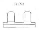
- FIG. 5A to FIG. 5Cshow yet another embodiment of the present invention wherein PR trimming and PR footing reduction are performed simultaneously prior to the deposition of the spacer oxide.
- This embodimentis similar to the embodiment described right above. However, this embodiment further includes reduction step of PR (photo resist) footing prior to spacer oxide film deposition.
- PR (photo resist) footing in the lower portions of the photo resist template patternmay be generated.
- the PR patternis exposed to a direct plasma in a PR footing reduction step so that activated ions like O 2 radical or Ar radical are accelerated towards the vertical direction, so trimming rate in the vertical direction (perpendicular to substrate and to electrode) is faster than in the horizontal direction (parallel to electrode) as shown in FIG. 5B . Therefore, the photo resist (PR) footing is reduced as shown in FIG. 5C .
- the line width of the photo resist template patterns and the spacing between lines of the photo resist template patternsare in a ratio of 1:C (wherein 1 ⁇ C ⁇ 3). In the example shown in FIG.
- This PR footing reduction step by direct plasma exposureresults, in addition to footing reduction, to PR trimming and can also be considered as a PR resist trimming step with improved characteristics. This process is performed in the same reactor chamber as wherein deposition is performed. If the PR footing has been adequately removed in the PR footing reduction step, but additional trimming is needed, an additional trimming step without direct plasma exposure can be performed, either before or after the PR reduction step but prior to deposition.
- a SiO 2 film deposition by PEALD on photo resist template patternsis carried out with the following conditions.
- Si precursorsMetalorganic precursors or halosilane precursors containing Si can be used as Si precursors.
- SiH 2 [N(C 2 H 5 ) 2 ] 2was used as a Si precursor.
- Susceptor temperature for heating substratevaried from room temperature to 200 degree C, preferably the susceptor temperature was 50 degree C.
- process pressureis maintained in a range from 1 to 10 Torr, preferably at a value of about 3Torr.
- RF plasma poweris in a range from 10 to 1000W, preferably at a value of about 100W to 150W.
- FIG. 6shows process sequence according to FIGs. 5A to 5C .
- Cycle for pre-trimming step for PR footing reductionis repeated and deposition is performed after that.
- Reactant like O 2is provided during the pre-trimming step and deposition step.
- Purge gas like Aris provided during the deposition step.
- Plasmais provided intermittently during the pre-trimming step and deposition step.
- the template patternPR or carbon-based film
- the reduction of width to heightcould lead to the weakening of the geometric structure, so the template pattern line could easily lean or collapse in the cleaning or wafer handling process after trimming.
- the trimming and the film depositionare performed simultaneously according to the above described embodiments of the present invention, the deposited film can support the template pattern and the template pattern can maintain its shape or structure even if the width of the template pattern is thinned to the level of 10nm.
- the coverage of deposited material on the substratechanges gradually from 0% to 100% (full coverage) along the number of deposition cycles.
- the simultaneously etching of a layer on which the spacer oxide film is depositedreduces and the apparent etching rate decelerates from a certain etching rate to zero etching rate. This deceleration of etching rate would help to control the very fine CD of the photo resist template patterns or carbon line.
- the etching rate at initial stage and sufficient controllability of CDcan be achieved due to the variation of etching rate from high to low (deceleration effect) as the spacer oxide coverage gets close to the full coverage starting from zero coverage.
Landscapes
- Engineering & Computer Science (AREA)
- Physics & Mathematics (AREA)
- Microelectronics & Electronic Packaging (AREA)
- Power Engineering (AREA)
- Condensed Matter Physics & Semiconductors (AREA)
- General Physics & Mathematics (AREA)
- Manufacturing & Machinery (AREA)
- Computer Hardware Design (AREA)
- Chemical & Material Sciences (AREA)
- Chemical Kinetics & Catalysis (AREA)
- Plasma & Fusion (AREA)
- Inorganic Chemistry (AREA)
- Drying Of Semiconductors (AREA)
- Formation Of Insulating Films (AREA)
- Exposure Of Semiconductors, Excluding Electron Or Ion Beam Exposure (AREA)
- Semiconductor Memories (AREA)
Description
- The present invention relates to a method of forming semiconductor patterns. More specifically, the present invention relates to a spacer defined double patterning (SDDP) process using a PEALD spacer oxide deposition process having trimming action.
- Due to the limit of resolution of the immersion ArF lithography, the method of Double Patterning is used in the chip patterning process for 3X nm half pitch and below.
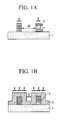
- In the art, the method of Spacer Defined Double Patterning, as represented in
FIGs. 1A-1D , is as follows. As shown inFIG. 1A , photoresist template patterns 2 are formed on top of abottom layer 1. Here, the line width and the line spacing are in a ratio of about 1:3. As shown inFIG. 1B , an oxide spacer conformal 3 is deposited on the photoresist template patterns 2. Here, the thickness of the oxide film is equal to the width of template line. - Next, as shown in
FIG. 1C , the depositedspacer oxide film 3 is etched back by RIE (reactive ion etching) such that film on the upper and bottom surfaces of pattern are removed andspacers 3a are formed on the side wall surfaces of the photoresist template patterns 2. - Then, as shown in
FIG. 1D , the photoresist template patterns 2 remaining between thespacers 3a are removed by selective etching and thebottom layer 1 is etched by using thespacers 3a as hard mask. - As single exposure lithography is very challenging in achieving 3X nm line widths and below, in the art a photo resist shrink step can be applied prior to the deposition of the spacer material as shown in
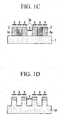
FIG. 2A to FIG. 2E . Firstly, first photoresist template patterns 22 are formed on top of abottom layer 11 as shown inFIG. 2A . Here, the ratio of line width X1 to spacing in between the lines of the first photoresist template patterns 22 is 1: A, wherein 1 ≦ A<3. The photoresist template patterns 22 are trimmed so that the line width of the photoresist template patterns 22 shrinks to form the second photoresist template patterns 22a as shown inFIG. 2B . Here, the line width X2 is about 1/3 of the line spacing of the second photoresist template patterns 22a. The trimming can be performed by an oxygen plasma or by thermal annealing in an inert ambient or in an oxidizing or reducing ambient. The trimming can be performed in a separate chamber or in-situ, in the same chamber in which the spacer oxide deposition is performed without removing the substrate from the chamber in between the trimming and deposition steps. - As shown in
FIG. 2C , an oxide spacer conformal 33 is deposited on the second photoresist template patterns 22a. Here, the thickness of theoxide film 33 is equal to the width of the second photoresist template patterns 22a. The depositedspacer oxide film 33 is etched back by RIE (reactive ion etching) such that thefilm 33 on the upper and bottom surfaces ofpatterns 22a are removed and film on the side wall surfaces of thepatterns 22a remain to bespacers 33a as shown inFIG. 2D . Then, as shown inFIG. 2E , the second photoresist template patterns 22a remaining betweenspacers 33a are removed by selective etching so that thespacers 33a remain and then thebottom layer 11 is patterned by using thespacers 33a as a hard mask (HM). - Through the above described sequence, the number of lines having the same width as the lines of the template after trimming is doubled and the pitch is halved. Instead of a spacer oxide, an alternative material, such as an oxynitride or a nitride material with suitable properties, could be selected.
- If the target Critical Dimension of lines is getting smaller than 30 nm, it will become difficult to control the uniformity of the amount of shrinking of such a photo resist shrink step or trimming step. Furthermore, there is a higher chance of patterning failure due to the leaning or collapsing of photo resist line due to the weak footing of the photo resist line when the photo resist line becomes narrower by the trimming.
- The article "Low temperature plasma-enhanced ALD enables cost-effective spacer defined double patterning (SDDP), by J. Beynet et al in Proc. of the SPIE, vol. 7520, 03 December 2009, pages 75201 J-75201J7, discloses the use of plasma-enhanced Atomic Layer Deposition for forming the spacers in the so called Spacer Defined Double Patterning (SDDP).
- The purpose of the invention is to secure measures to solve the problems which could occur in performing such a trimming step and to provide a Spacer Defined Double Patterning processes for 3X nm and below that avoids the problems discussed above.
- To solve the problems, trimming is performed simultaneously with the process of depositing the spacer oxide. In an alternative embodiment, a first part of the trimming is performedin-situ, immediately before the spacer oxide deposition process in the same chamber in which the spacer oxide deposition is performed whereas a second part of the trimming is performed simultaneously with the process of depositing the spacer oxide. The present invention also provides a method to reduce PR footing during PR trimming with direct plasma exposure.
- In an embodiment of the invention, trimming is performed simultaneously with the process of depositing the spacer oxide. The spacer oxide deposition process is a Plasma Enhanced Atomic Layer Deposition process.
- In another embodiment of the invention, a first part of the trimming is performedin-situ, immediately before the spacer oxide deposition process in the same chamber in which the spacer oxide deposition is performed whereas a second part of the trimming is performed simultaneously with the process of depositing the spacer oxide. The first part of the trimming is preferably performed by a continuous oxygen plasma or by a pulsed oxygen plasma. The spacer oxide deposition process is a Plasma Enhanced Atomic Layer deposition process.
- In another embodiment of the invention, PR trimming process under direct plasma makes PR footing reduce. This process includes two steps: a first step of PR trimming under direct plasma environment without supplying a precursor, a second step of deposition of SiO2 film. In a direct plasma generated between a susceptor electrode grounded on earth on which the substrate is placed and an opposing electrode such as a shower head electrode, activated ions are accelerated in a vertical direction towards the substrate placed on the susceptor electrode and lead to higher trimming rate towards vertical direction than horizontal direction on the PR so that PR footing remaining in the bottom of PR is reduced.
- The present invention will become more apparent by describing embodiments thereof in detail with reference to the accompanying drawing in which:
FIG. 1A to FIG. 1D show a Prior Art method of Spacer Defined Double Patterning without trimming.FIG. 2a to FIG. 2E show a Prior Art method of Spacer Defined Double Patterning with trimming prior to spacer deposition.FIG. 3A to FIG. 3D show an embodiment of the present invention wherein trimming is preformed during the deposition of the spacer oxide.FIG. 4A to FIG. 4E show another embodiment of the present invention wherein trimming is performed both prior to and during the deposition of the spacer oxide.FIG. 5A to FIG. 5C show yet another embodiment of the present invention wherein PR trimming and PR footing reduction are performed simultaneously prior to the deposition of the spacer oxide.FIG. 6 shows process sequence according toFIGs. 5A-5C .- The present invention will be described more fully hereinafter with reference to the accompanying drawings, in which exemplary embodiments of the invention are shown.
- In the drawings, the thickness of layers, films, panels, regions, etc., are exaggerated for clarity. Like reference numerals designate like elements throughout the specification. It will be understood that when an element such as a layer, film, region, or substrate is referred to as being "on' another element, it can be directly on the other element or intervening elements may also be present. In contrast, when an element is referred to as being "directly on" another element, there are no intervening elements present.
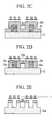
FIG. 3A to FIG. 3D show an embodiment of the present invention wherein trimming is simultaneously preformed during the deposition of the spacer oxide. As shown inFIG. 3A , first photo resist or carbon basedmaterial template patterns 120 are on top of abottom layer 110. Here, the ratio of line width XX to line spacing of the first photo resisttemplate patterns 120 is 1: A (1≦ A<3).- As shown in
FIG. 3B , aspacer oxide film 130 is deposited on the formed first photo resisttemplate patterns 120 and simultaneously second photo resisttemplate patterns 120a having a width XX2 and a height Y2 that is smaller than the width XX and the height Y of the first photo resisttemplate patterns 120 are formed, using a Plasma Enhanced Atomic Layer Deposition process using sequential and alternating pulses of source gas such as a silicon precursor and reactant such as O2 plasma. In this step, the O2 plasma should be provided with a condition that: (i) thefirst template patterns 120 can be etched with a certain etching rate such that the first photo resisttemplate patterns 120 are trimmed to form the second photo resisttemplate patterns 120a and (ii) oxygen radical can be reacted with a precursor deposited previously on the substrate to form thespacer oxide film 130 such as SiO2 film by PEALD method. At the end of this step, a ratio of the line width to line spacing of the second photo resisttemplate patterns 120a should be 1:3 and the thickness of the depositedspacer oxide film 130 should be equal to the width of the second photo resisttemplate patterns 120a. The O2 plasma may be a direct plasma wherein the plasma is generated immediately adjacent to the substrate or a remote plasma. - Then, the deposited
spacer oxide film 130 is etched back by RIE such that the depositedspacer oxide film 130 on the upper and bottom surfaces ofpatterns 120a is removed and the depositedspacer oxide film 130 on the side wall surfaces of thepatterns 120a remains to bespacers 130a as shown inFIG. 3C . - Subsequently, as shown in
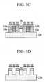
FIG. 3D , the second photo resisttemplate patterns 120a remaining between thespacers 130a are removed by selective etching such that thespacers 130a remain. Then, thebottom layer 110 is patterned by using thespacers 130a as a hard mask (HM). FIG. 4A to FIG. 4E show another embodiment of the present invention wherein trimming is simultaneously preformed during the deposition of the spacer oxide film. Firstly, as shown inFIG. 4A , first photo resist or carbon basedmaterial template patterns 120 are formed on top of abottom layer 110. Here, the ratio of line width XX to spacing in between the lines of the first photo resisttemplate patterns 120 is 1: A (1≦A<3).- Next, , as shown in
FIG. 4B , the first photo resisttemplate patterns 120 are firstly trimmed so that the line width shrinks to form third photo resist template patterns 120aa having a line width XX1 (wherein XX1 <XX). Here, the ratio of line width XX1 to spacing in between the lines of the third photo resist template patterns 120aa is 1: B (wherein A<B<3). The first trimming can be performed by an oxygen plasma (direct plasma or remote plasma) or by thermal annealing in an inert ambient or in an oxidizing or reducing ambient. Preferably, the first trimming is performed in-situ, in the same chamber in which the spacer oxide deposition is performed without removing the substrate from the chamber between the trimming and deposition steps. - Next, as shown in
FIG. 4C , aspacer oxide film 130 is deposited on the third photo resist template patterns 120aa and the third photo resist template patterns 120aa are simultaneously secondly trimmed so that fourth photo resisttemplate patterns 120b having a width XX2 and a height Y2 that is smaller than the width XX1, the height Y of the first photo resisttemplate patterns 120, and the height Y1 of the third photo resist template patterns 120aa are formed, using a Plasma Enhanced Atomic Layer Deposition process using sequential and alternating pulses of source gas such as a silicon precursor and reactant such as O2 plasma. In this step, the O2 plasma should be provided with a condition that: (i) the third template patterns 120aa can be etched with a certain etching rate such that the third template patterns 120aa are trimmed to form the fourth photo resisttemplate patterns 120b and (ii) oxygen radical can be reacted with precursor deposited previously on the substrate to form thespacer oxide film 130 such as SiO2 film by PEALD method. At the end of this step, the photo resist pattern lines have shrunk to a width XX2 (wherein XX2 < XX1) and the ratio of line width XX2 to line spacing should be 1:3 and the thickness of the depositedspacer oxide film 130 should be equal to width XX2 of the fourth photo resisttemplate patterns 120b. Here, the O2 plasma may be a direct plasma or a remote plasma. - As shown in
FIG. 4D , the depositedspacer oxide film 130 is etched back by RIE such that thefilm 130 on the upper and bottom surfaces of the fourth photo resisttemplate patterns 120b are removed and thefilm 130 remains on the side wall surfaces of the fourth photo resisttemplate patterns 120b to be spacers 130a. - As shown in
FIG. 4E , the fourth photo resisttemplate patterns 120b remaining between thespacers 130a are removed by selective etching such that thespacers 130a remain. Then, thebottom layer 110 is patterned by using thespacers 130a as a hard mask (HM). - The trimming of the photo resist template patterns during the PEALD process of the spacer oxide film might occur in particular during the initial cycles of the deposition process. When multiple cycles of the spacer oxide have been deposited, the photo resist template patterns might be protected from the O2 plasma so that further etching and shrinking of the photo resist does not occur anymore and only spacer oxide deposition occurs. The conditions of the spacer oxide deposition process and an eventual trimming step prior to the spacer oxide deposition should be selected such that after completion of the spacer oxide template: line width = line space = film thickness.
- In the description below, the pressure is indicated in Torr, wherein 1 Torr equals 133 Pa.
- A SiO2 film deposition by PEALD on photo resist template patterns is carried out with the following conditions.
- Metalorganic precursors or halosilane precursors containing Si can be used as Si precursors. In the present invention, for example, SiH2[N(C2H5)2]2 was used as a Si precursor. Susceptor temperature for heating substrate varied from room temperature to 200 degree C, preferably the susceptor temperature was 50 degree C. During deposition, process pressure is maintained in a range from 1 to 10 Torr, preferably at a value of about 3Torr. RF plasma power is in a range from 10 to 1000W, preferably at a value of about 200W.
- Gas flow condition is as follows.
- Source Ar flow rate for carrying bubbled precursor into reactor : 200sccm
- Temperature of precursor container: 60°C
- O2 reactant flow rate: 50sccm
- Reactant Ar flow rate for flowing into reactor with oxygen: 200sccm
- Main Ar flow rate for chamber / gas line purge: 200sccm
- Process time per cycle is as follows.
- - Source feeding /Purge /Plasma /Purge = 1.0 / 1.0/ 0.3/ 1.0 (unit: second) In the above sequence, oxygen is continuously provided during all steps of the cycle and activated when plasma is provided. When not activated by the plasma, the oxygen is not reactive and just acts as a purge gas. In an alternative embodiment, the oxygen can also be provided intermittently, synchronously with the plasma pulses. The above cycle is repeated until a target thickness is achieved. The deposited film thickness per cycle is about 0.12 nm.
- For a photo resist trimming step prior to the PEALD deposition step, similar conditions can be used as during the PEALD step but without flowing the Silicon precursor. The photo resist film thickness reduction for a blanket photo resist layer would be about 0.25 nm per cycle. Then, after a number of cycles comprising oxygen plasma pulses resulting in an initial thinning of the photo resist lines, the Silicon precursor flow can be switched on and some additional photo resist line width reduction can be obtained during the PEALD deposition step. In a first example, the width of the photo resist lines, or critical dimension (CD) directly after lithography is 40 nm and the line spacing is also 40 nm. During an in-situ trimming step prior to deposition, a CD reduction down to 25 nm is achieved. In a subsequent spacer deposition step of 20 nm thickness, an additional reduction of the CD from 25 nm down to 20 nm is achieved. In a second example, the critical dimension of the photo resist lines is 30 nm directly after lithography and the line spacing is 30 nm. During an in-situ trimming step prior to a spacer deposition step, a reduction of photo resist CD down to 20 nm is achieved. Then, during a 15 nm spacer oxide PEALD step, a further reduction of photo resist CD from 20 nm down to 15 nm is achieved.
FIG. 5A to FIG. 5C show yet another embodiment of the present invention wherein PR trimming and PR footing reduction are performed simultaneously prior to the deposition of the spacer oxide. This embodiment is similar to the embodiment described right above. However, this embodiment further includes reduction step of PR (photo resist) footing prior to spacer oxide film deposition.- As shown in
FIG. 5A , PR (photo resist) footing in the lower portions of the photo resist template pattern may be generated. During the trimming step, the PR pattern is exposed to a direct plasma in a PR footing reduction step so that activated ions like O2 radical or Ar radical are accelerated towards the vertical direction, so trimming rate in the vertical direction (perpendicular to substrate and to electrode) is faster than in the horizontal direction (parallel to electrode) as shown inFIG. 5B . Therefore, the photo resist (PR) footing is reduced as shown inFIG. 5C . In this embodiment, the line width of the photo resist template patterns and the spacing between lines of the photo resist template patterns are in a ratio of 1:C (wherein 1≤ C <3). In the example shown inFIG. 5C , C is about 1. This PR footing reduction step by direct plasma exposure results, in addition to footing reduction, to PR trimming and can also be considered as a PR resist trimming step with improved characteristics. This process is performed in the same reactor chamber as wherein deposition is performed. If the PR footing has been adequately removed in the PR footing reduction step, but additional trimming is needed, an additional trimming step without direct plasma exposure can be performed, either before or after the PR reduction step but prior to deposition. - A SiO2 film deposition by PEALD on photo resist template patterns is carried out with the following conditions.
- Metalorganic precursors or halosilane precursors containing Si can be used as Si precursors. In this invention, SiH2[N(C2H5)2]2 was used as a Si precursor. Susceptor temperature for heating substrate varied from room temperature to 200 degree C, preferably the susceptor temperature was 50 degree C. During deposition, process pressure is maintained in a range from 1 to 10 Torr, preferably at a value of about 3Torr. RF plasma power is in a range from 10 to 1000W, preferably at a value of about 100W to 150W.
- Gas flow condition:
- Source Ar flow rate for carrying bubbled precursor into reactor : 500sccm
- Temperature of precursor container: 60°C
- O2 reactant flow rate: 1000 sccm
- Reactant Ar flow rate for flowing into reactor with oxygen: 500sccm
- Main Ar flow rate for chamber / gas line purge: 200sccm
- Reaction space gap between showerhead and substrate: 14.5mm.
- Processing time:
- Pre-trimming step : <2.0sec.
- Deposition step time : <2.0sec.
- Plasma pulsing time : 0.2sec
- Purge time : 1.0sec.
FIG. 6 shows process sequence according toFIGs. 5A to 5C . Cycle for pre-trimming step for PR footing reduction is repeated and deposition is performed after that. Reactant like O2 is provided during the pre-trimming step and deposition step. Purge gas like Ar is provided during the deposition step. Plasma is provided intermittently during the pre-trimming step and deposition step.- The advantages of the present invention are as follows, compared to the case of performing trimming separately in advance.
- If the template pattern (PR or carbon-based film) is trimmed to a width of 1X (10 to 19 nm) in a separate etching chamber, the reduction of width to height could lead to the weakening of the geometric structure, so the template pattern line could easily lean or collapse in the cleaning or wafer handling process after trimming. However, if the trimming and the film deposition are performed simultaneously according to the above described embodiments of the present invention, the deposited film can support the template pattern and the template pattern can maintain its shape or structure even if the width of the template pattern is thinned to the level of 10nm.
- Combining the trimming and the deposition process results in a simpler and more efficient process.
- In ALD, the coverage of deposited material on the substrate changes gradually from 0% to 100% (full coverage) along the number of deposition cycles. As the coverage changes along the deposition, the simultaneously etching of a layer on which the spacer oxide film is deposited (photo resist or carbon template patterns in this invention) reduces and the apparent etching rate decelerates from a certain etching rate to zero etching rate. This deceleration of etching rate would help to control the very fine CD of the photo resist template patterns or carbon line. In prior art of dry etching, it would be very difficult to control the etching amount precisely with controlled time. If the overall etching rate is low, it would impact on the productivity, and if the etching rate is fast, it would impact on the controllability of CD. But, according to the present invention, by implementing the simultaneous etching and deposition, the sufficient etching rate at initial stage and sufficient controllability of CD can be achieved due to the variation of etching rate from high to low (deceleration effect) as the spacer oxide coverage gets close to the full coverage starting from zero coverage.
- PR trimming process under direct plasma prior to deposition step leads to the reduction of PR footing as activated species is accelerated more towards the vertical direction than the horizontal direction on PR so that trimming rate is faster in the vertical direction than the horizontal direction on PR. This leads to better trimming and improves film uniformity in the deposition step.
Claims (10)
- A method of forming semiconductor patterns, the method comprising:forming a photo resist template having a pattern of lines on a bottom layer, the pattern having a line width and a line spacing, the ratio of the line width to the line spacing being 1: A wherein 1≦ A <3;depositing a spacer oxide conformal over the photo resist template by a Plasma Enhanced Atomic Layer deposition process, using sequential and alternating pulses of a silicon precursor and an oxygen plasma, such that trimming of the photo resist template occurs and the ratio of the line width to the line spacing becomes 1:3 and the thickness of the deposited spacer oxide is about equal to the trimmed line width;etching back the deposited spacer oxide such that spacer oxide films on upper and bottom surfaces of the pattern are removed, with spacer oxide films on side wall surfaces of the photo resist template remaining;removing the photo resist template remaining between the spacer oxide films by selective etching; andpatterning the bottom layer by using the remaining spacer oxide films formed as mask.
- The method of claim 1, further comprising: trimming, prior to the step of depositing the spacer oxide, the photo resist pattern of lines such that the ratio of the line width to the line spacing becomes 1: B, wherein A<B<3 by exposing the photo resist pattern of lines to pulses of the oxygen plasma, in the same reaction chamber in which the spacer oxide deposition is performed.
- The method of claim 2, further comprising: a PR footing reduction step prior to the step of depositing the spacer oxide, in the same reaction chamber in which PR trimming step and the spacer oxide deposition step are performed, the PR footing reduction step comprising a direct plasma exposure step.
- The method of claim 3, wherein the PR footing reduction step is performed prior to the PR trimming step.
- The method of claim 3, wherein the PR footing reduction step is performed after the PR trimming step.
- The method of claim 1, wherein the plasma is a direct plasma.
- The method of claim 1, wherein the plasma is a remote plasma.
- The method of claim 2, wherein the plasma is a direct plasma.
- The method of claim 2, wherein the plasma is a remote plasma.
- The method of claim 1, wherein the silicon precursor is SiH2[N(C2H5)2]2.
Applications Claiming Priority (1)
| Application Number | Priority Date | Filing Date | Title |
|---|---|---|---|
| US32391810P | 2010-04-14 | 2010-04-14 |
Publications (3)
| Publication Number | Publication Date |
|---|---|
| EP2378543A2 EP2378543A2 (en) | 2011-10-19 |
| EP2378543A3 EP2378543A3 (en) | 2014-05-28 |
| EP2378543B1true EP2378543B1 (en) | 2015-05-20 |
Family
ID=44343653
Family Applications (1)
| Application Number | Title | Priority Date | Filing Date |
|---|---|---|---|
| EP20110162225ActiveEP2378543B1 (en) | 2010-04-14 | 2011-04-13 | Method of forming semiconductor patterns |
Country Status (5)
| Country | Link |
|---|---|
| US (2) | US8252691B2 (en) |
| EP (1) | EP2378543B1 (en) |
| JP (1) | JP5756325B2 (en) |
| KR (1) | KR101779112B1 (en) |
| TW (1) | TWI523070B (en) |
Families Citing this family (403)
| Publication number | Priority date | Publication date | Assignee | Title |
|---|---|---|---|---|
| US10378106B2 (en) | 2008-11-14 | 2019-08-13 | Asm Ip Holding B.V. | Method of forming insulation film by modified PEALD |
| US9394608B2 (en) | 2009-04-06 | 2016-07-19 | Asm America, Inc. | Semiconductor processing reactor and components thereof |
| US8802201B2 (en) | 2009-08-14 | 2014-08-12 | Asm America, Inc. | Systems and methods for thin-film deposition of metal oxides using excited nitrogen-oxygen species |
| US9312155B2 (en) | 2011-06-06 | 2016-04-12 | Asm Japan K.K. | High-throughput semiconductor-processing apparatus equipped with multiple dual-chamber modules |
| US9793148B2 (en) | 2011-06-22 | 2017-10-17 | Asm Japan K.K. | Method for positioning wafers in multiple wafer transport |
| US10364496B2 (en) | 2011-06-27 | 2019-07-30 | Asm Ip Holding B.V. | Dual section module having shared and unshared mass flow controllers |
| US10854498B2 (en) | 2011-07-15 | 2020-12-01 | Asm Ip Holding B.V. | Wafer-supporting device and method for producing same |
| US20130023129A1 (en) | 2011-07-20 | 2013-01-24 | Asm America, Inc. | Pressure transmitter for a semiconductor processing environment |
| US9017481B1 (en) | 2011-10-28 | 2015-04-28 | Asm America, Inc. | Process feed management for semiconductor substrate processing |
| US8946830B2 (en) | 2012-04-04 | 2015-02-03 | Asm Ip Holdings B.V. | Metal oxide protective layer for a semiconductor device |
| JP6089451B2 (en)* | 2012-05-30 | 2017-03-08 | 大日本印刷株式会社 | Nanoimprint mold and manufacturing method thereof |
| JP6015140B2 (en)* | 2012-06-01 | 2016-10-26 | 大日本印刷株式会社 | Nanoimprint mold and manufacturing method thereof |
| US9558931B2 (en) | 2012-07-27 | 2017-01-31 | Asm Ip Holding B.V. | System and method for gas-phase sulfur passivation of a semiconductor surface |
| US9659799B2 (en) | 2012-08-28 | 2017-05-23 | Asm Ip Holding B.V. | Systems and methods for dynamic semiconductor process scheduling |
| US9021985B2 (en) | 2012-09-12 | 2015-05-05 | Asm Ip Holdings B.V. | Process gas management for an inductively-coupled plasma deposition reactor |
| CN103681250B (en)* | 2012-09-17 | 2016-08-17 | 上海华虹宏力半导体制造有限公司 | The control method of the critical size of twice etching molding figure |
| US9324811B2 (en) | 2012-09-26 | 2016-04-26 | Asm Ip Holding B.V. | Structures and devices including a tensile-stressed silicon arsenic layer and methods of forming same |
| US10714315B2 (en) | 2012-10-12 | 2020-07-14 | Asm Ip Holdings B.V. | Semiconductor reaction chamber showerhead |
| JP6003571B2 (en)* | 2012-11-21 | 2016-10-05 | 大日本印刷株式会社 | Method for producing template for nanoimprint |
| US9640416B2 (en) | 2012-12-26 | 2017-05-02 | Asm Ip Holding B.V. | Single-and dual-chamber module-attachable wafer-handling chamber |
| US20160376700A1 (en) | 2013-02-01 | 2016-12-29 | Asm Ip Holding B.V. | System for treatment of deposition reactor |
| US9484191B2 (en) | 2013-03-08 | 2016-11-01 | Asm Ip Holding B.V. | Pulsed remote plasma method and system |
| US9589770B2 (en) | 2013-03-08 | 2017-03-07 | Asm Ip Holding B.V. | Method and systems for in-situ formation of intermediate reactive species |
| US8993054B2 (en) | 2013-07-12 | 2015-03-31 | Asm Ip Holding B.V. | Method and system to reduce outgassing in a reaction chamber |
| US9018111B2 (en) | 2013-07-22 | 2015-04-28 | Asm Ip Holding B.V. | Semiconductor reaction chamber with plasma capabilities |
| US9793115B2 (en) | 2013-08-14 | 2017-10-17 | Asm Ip Holding B.V. | Structures and devices including germanium-tin films and methods of forming same |
| US9240412B2 (en) | 2013-09-27 | 2016-01-19 | Asm Ip Holding B.V. | Semiconductor structure and device and methods of forming same using selective epitaxial process |
| US9556516B2 (en) | 2013-10-09 | 2017-01-31 | ASM IP Holding B.V | Method for forming Ti-containing film by PEALD using TDMAT or TDEAT |
| US9343308B2 (en)* | 2013-10-28 | 2016-05-17 | Asm Ip Holding B.V. | Method for trimming carbon-containing film at reduced trimming rate |
| US10179947B2 (en) | 2013-11-26 | 2019-01-15 | Asm Ip Holding B.V. | Method for forming conformal nitrided, oxidized, or carbonized dielectric film by atomic layer deposition |
| JP2015154034A (en)* | 2014-02-19 | 2015-08-24 | 株式会社東芝 | Deposition device and deposition method |
| US10683571B2 (en) | 2014-02-25 | 2020-06-16 | Asm Ip Holding B.V. | Gas supply manifold and method of supplying gases to chamber using same |
| US9447498B2 (en) | 2014-03-18 | 2016-09-20 | Asm Ip Holding B.V. | Method for performing uniform processing in gas system-sharing multiple reaction chambers |
| US10167557B2 (en) | 2014-03-18 | 2019-01-01 | Asm Ip Holding B.V. | Gas distribution system, reactor including the system, and methods of using the same |
| US11015245B2 (en) | 2014-03-19 | 2021-05-25 | Asm Ip Holding B.V. | Gas-phase reactor and system having exhaust plenum and components thereof |
| US9404587B2 (en) | 2014-04-24 | 2016-08-02 | ASM IP Holding B.V | Lockout tagout for semiconductor vacuum valve |
| US10858737B2 (en) | 2014-07-28 | 2020-12-08 | Asm Ip Holding B.V. | Showerhead assembly and components thereof |
| US9543180B2 (en) | 2014-08-01 | 2017-01-10 | Asm Ip Holding B.V. | Apparatus and method for transporting wafers between wafer carrier and process tool under vacuum |
| US9890456B2 (en) | 2014-08-21 | 2018-02-13 | Asm Ip Holding B.V. | Method and system for in situ formation of gas-phase compounds |
| US9657845B2 (en) | 2014-10-07 | 2017-05-23 | Asm Ip Holding B.V. | Variable conductance gas distribution apparatus and method |
| US10941490B2 (en) | 2014-10-07 | 2021-03-09 | Asm Ip Holding B.V. | Multiple temperature range susceptor, assembly, reactor and system including the susceptor, and methods of using the same |
| JP6382055B2 (en)* | 2014-10-07 | 2018-08-29 | 東京エレクトロン株式会社 | Method for processing an object |
| KR102300403B1 (en) | 2014-11-19 | 2021-09-09 | 에이에스엠 아이피 홀딩 비.브이. | Method of depositing thin film |
| KR102263121B1 (en) | 2014-12-22 | 2021-06-09 | 에이에스엠 아이피 홀딩 비.브이. | Semiconductor device and manufacuring method thereof |
| US9318478B1 (en) | 2015-01-30 | 2016-04-19 | Samsung Electronics Co., Ltd. | Semiconductor device and fabricating method thereof |
| JP6559430B2 (en)* | 2015-01-30 | 2019-08-14 | 東京エレクトロン株式会社 | Method for processing an object |
| US9478415B2 (en) | 2015-02-13 | 2016-10-25 | Asm Ip Holding B.V. | Method for forming film having low resistance and shallow junction depth |
| US10529542B2 (en) | 2015-03-11 | 2020-01-07 | Asm Ip Holdings B.V. | Cross-flow reactor and method |
| US10276355B2 (en) | 2015-03-12 | 2019-04-30 | Asm Ip Holding B.V. | Multi-zone reactor, system including the reactor, and method of using the same |
| EP3101682A1 (en)* | 2015-06-03 | 2016-12-07 | IMEC vzw | Method for providing a patterned target layer in a semiconductor structure |
| US10458018B2 (en) | 2015-06-26 | 2019-10-29 | Asm Ip Holding B.V. | Structures including metal carbide material, devices including the structures, and methods of forming same |
| US10600673B2 (en) | 2015-07-07 | 2020-03-24 | Asm Ip Holding B.V. | Magnetic susceptor to baseplate seal |
| US9899291B2 (en) | 2015-07-13 | 2018-02-20 | Asm Ip Holding B.V. | Method for protecting layer by forming hydrocarbon-based extremely thin film |
| US10043661B2 (en) | 2015-07-13 | 2018-08-07 | Asm Ip Holding B.V. | Method for protecting layer by forming hydrocarbon-based extremely thin film |
| US10083836B2 (en) | 2015-07-24 | 2018-09-25 | Asm Ip Holding B.V. | Formation of boron-doped titanium metal films with high work function |
| US10087525B2 (en) | 2015-08-04 | 2018-10-02 | Asm Ip Holding B.V. | Variable gap hard stop design |
| US9711359B2 (en)* | 2015-08-13 | 2017-07-18 | Lam Research Corporation | Shadow trim line edge roughness reduction |
| US9647114B2 (en) | 2015-08-14 | 2017-05-09 | Asm Ip Holding B.V. | Methods of forming highly p-type doped germanium tin films and structures and devices including the films |
| US9711345B2 (en) | 2015-08-25 | 2017-07-18 | Asm Ip Holding B.V. | Method for forming aluminum nitride-based film by PEALD |
| US9960072B2 (en) | 2015-09-29 | 2018-05-01 | Asm Ip Holding B.V. | Variable adjustment for precise matching of multiple chamber cavity housings |
| US9909214B2 (en) | 2015-10-15 | 2018-03-06 | Asm Ip Holding B.V. | Method for depositing dielectric film in trenches by PEALD |
| US10211308B2 (en) | 2015-10-21 | 2019-02-19 | Asm Ip Holding B.V. | NbMC layers |
| US10322384B2 (en) | 2015-11-09 | 2019-06-18 | Asm Ip Holding B.V. | Counter flow mixer for process chamber |
| US9455138B1 (en) | 2015-11-10 | 2016-09-27 | Asm Ip Holding B.V. | Method for forming dielectric film in trenches by PEALD using H-containing gas |
| US9905420B2 (en) | 2015-12-01 | 2018-02-27 | Asm Ip Holding B.V. | Methods of forming silicon germanium tin films and structures and devices including the films |
| US9607837B1 (en) | 2015-12-21 | 2017-03-28 | Asm Ip Holding B.V. | Method for forming silicon oxide cap layer for solid state diffusion process |
| US9735024B2 (en) | 2015-12-28 | 2017-08-15 | Asm Ip Holding B.V. | Method of atomic layer etching using functional group-containing fluorocarbon |
| US9627221B1 (en) | 2015-12-28 | 2017-04-18 | Asm Ip Holding B.V. | Continuous process incorporating atomic layer etching |
| US11139308B2 (en) | 2015-12-29 | 2021-10-05 | Asm Ip Holding B.V. | Atomic layer deposition of III-V compounds to form V-NAND devices |
| US10157742B2 (en)* | 2015-12-31 | 2018-12-18 | Taiwan Semiconductor Manufacturing Co., Ltd. | Method for mandrel and spacer patterning |
| US10529554B2 (en) | 2016-02-19 | 2020-01-07 | Asm Ip Holding B.V. | Method for forming silicon nitride film selectively on sidewalls or flat surfaces of trenches |
| US10468251B2 (en) | 2016-02-19 | 2019-11-05 | Asm Ip Holding B.V. | Method for forming spacers using silicon nitride film for spacer-defined multiple patterning |
| US9754779B1 (en) | 2016-02-19 | 2017-09-05 | Asm Ip Holding B.V. | Method for forming silicon nitride film selectively on sidewalls or flat surfaces of trenches |
| US10501866B2 (en) | 2016-03-09 | 2019-12-10 | Asm Ip Holding B.V. | Gas distribution apparatus for improved film uniformity in an epitaxial system |
| US10343920B2 (en) | 2016-03-18 | 2019-07-09 | Asm Ip Holding B.V. | Aligned carbon nanotubes |
| US9892913B2 (en) | 2016-03-24 | 2018-02-13 | Asm Ip Holding B.V. | Radial and thickness control via biased multi-port injection settings |
| US10190213B2 (en) | 2016-04-21 | 2019-01-29 | Asm Ip Holding B.V. | Deposition of metal borides |
| US10865475B2 (en) | 2016-04-21 | 2020-12-15 | Asm Ip Holding B.V. | Deposition of metal borides and silicides |
| US10087522B2 (en) | 2016-04-21 | 2018-10-02 | Asm Ip Holding B.V. | Deposition of metal borides |
| US10367080B2 (en) | 2016-05-02 | 2019-07-30 | Asm Ip Holding B.V. | Method of forming a germanium oxynitride film |
| US10032628B2 (en) | 2016-05-02 | 2018-07-24 | Asm Ip Holding B.V. | Source/drain performance through conformal solid state doping |
| KR102592471B1 (en) | 2016-05-17 | 2023-10-20 | 에이에스엠 아이피 홀딩 비.브이. | Method of forming metal interconnection and method of fabricating semiconductor device using the same |
| US11453943B2 (en) | 2016-05-25 | 2022-09-27 | Asm Ip Holding B.V. | Method for forming carbon-containing silicon/metal oxide or nitride film by ALD using silicon precursor and hydrocarbon precursor |
| US10388509B2 (en) | 2016-06-28 | 2019-08-20 | Asm Ip Holding B.V. | Formation of epitaxial layers via dislocation filtering |
| US9859151B1 (en) | 2016-07-08 | 2018-01-02 | Asm Ip Holding B.V. | Selective film deposition method to form air gaps |
| US10612137B2 (en) | 2016-07-08 | 2020-04-07 | Asm Ip Holdings B.V. | Organic reactants for atomic layer deposition |
| US9793135B1 (en) | 2016-07-14 | 2017-10-17 | ASM IP Holding B.V | Method of cyclic dry etching using etchant film |
| US10714385B2 (en) | 2016-07-19 | 2020-07-14 | Asm Ip Holding B.V. | Selective deposition of tungsten |
| KR102354490B1 (en) | 2016-07-27 | 2022-01-21 | 에이에스엠 아이피 홀딩 비.브이. | Method of processing a substrate |
| KR102532607B1 (en) | 2016-07-28 | 2023-05-15 | 에이에스엠 아이피 홀딩 비.브이. | Substrate processing apparatus and method of operating the same |
| US9812320B1 (en) | 2016-07-28 | 2017-11-07 | Asm Ip Holding B.V. | Method and apparatus for filling a gap |
| US9887082B1 (en) | 2016-07-28 | 2018-02-06 | Asm Ip Holding B.V. | Method and apparatus for filling a gap |
| US10177025B2 (en) | 2016-07-28 | 2019-01-08 | Asm Ip Holding B.V. | Method and apparatus for filling a gap |
| US10395919B2 (en) | 2016-07-28 | 2019-08-27 | Asm Ip Holding B.V. | Method and apparatus for filling a gap |
| US10090316B2 (en) | 2016-09-01 | 2018-10-02 | Asm Ip Holding B.V. | 3D stacked multilayer semiconductor memory using doped select transistor channel |
| US10229832B2 (en)* | 2016-09-22 | 2019-03-12 | Varian Semiconductor Equipment Associates, Inc. | Techniques for forming patterned features using directional ions |
| US10410943B2 (en) | 2016-10-13 | 2019-09-10 | Asm Ip Holding B.V. | Method for passivating a surface of a semiconductor and related systems |
| US10643826B2 (en) | 2016-10-26 | 2020-05-05 | Asm Ip Holdings B.V. | Methods for thermally calibrating reaction chambers |
| US11532757B2 (en) | 2016-10-27 | 2022-12-20 | Asm Ip Holding B.V. | Deposition of charge trapping layers |
| US10229833B2 (en) | 2016-11-01 | 2019-03-12 | Asm Ip Holding B.V. | Methods for forming a transition metal nitride film on a substrate by atomic layer deposition and related semiconductor device structures |
| US10643904B2 (en) | 2016-11-01 | 2020-05-05 | Asm Ip Holdings B.V. | Methods for forming a semiconductor device and related semiconductor device structures |
| US10435790B2 (en) | 2016-11-01 | 2019-10-08 | Asm Ip Holding B.V. | Method of subatmospheric plasma-enhanced ALD using capacitively coupled electrodes with narrow gap |
| US10714350B2 (en) | 2016-11-01 | 2020-07-14 | ASM IP Holdings, B.V. | Methods for forming a transition metal niobium nitride film on a substrate by atomic layer deposition and related semiconductor device structures |
| US10134757B2 (en) | 2016-11-07 | 2018-11-20 | Asm Ip Holding B.V. | Method of processing a substrate and a device manufactured by using the method |
| KR102546317B1 (en) | 2016-11-15 | 2023-06-21 | 에이에스엠 아이피 홀딩 비.브이. | Gas supply unit and substrate processing apparatus including the same |
| US10340135B2 (en) | 2016-11-28 | 2019-07-02 | Asm Ip Holding B.V. | Method of topologically restricted plasma-enhanced cyclic deposition of silicon or metal nitride |
| KR102762543B1 (en) | 2016-12-14 | 2025-02-05 | 에이에스엠 아이피 홀딩 비.브이. | Substrate processing apparatus |
| US9916980B1 (en) | 2016-12-15 | 2018-03-13 | Asm Ip Holding B.V. | Method of forming a structure on a substrate |
| US11581186B2 (en) | 2016-12-15 | 2023-02-14 | Asm Ip Holding B.V. | Sequential infiltration synthesis apparatus |
| US11447861B2 (en) | 2016-12-15 | 2022-09-20 | Asm Ip Holding B.V. | Sequential infiltration synthesis apparatus and a method of forming a patterned structure |
| KR102700194B1 (en) | 2016-12-19 | 2024-08-28 | 에이에스엠 아이피 홀딩 비.브이. | Substrate processing apparatus |
| US10269558B2 (en) | 2016-12-22 | 2019-04-23 | Asm Ip Holding B.V. | Method of forming a structure on a substrate |
| US10867788B2 (en) | 2016-12-28 | 2020-12-15 | Asm Ip Holding B.V. | Method of forming a structure on a substrate |
| US11390950B2 (en) | 2017-01-10 | 2022-07-19 | Asm Ip Holding B.V. | Reactor system and method to reduce residue buildup during a film deposition process |
| US10655221B2 (en) | 2017-02-09 | 2020-05-19 | Asm Ip Holding B.V. | Method for depositing oxide film by thermal ALD and PEALD |
| US10468261B2 (en) | 2017-02-15 | 2019-11-05 | Asm Ip Holding B.V. | Methods for forming a metallic film on a substrate by cyclical deposition and related semiconductor device structures |
| US10529563B2 (en) | 2017-03-29 | 2020-01-07 | Asm Ip Holdings B.V. | Method for forming doped metal oxide films on a substrate by cyclical deposition and related semiconductor device structures |
| US10283353B2 (en) | 2017-03-29 | 2019-05-07 | Asm Ip Holding B.V. | Method of reforming insulating film deposited on substrate with recess pattern |
| US10103040B1 (en) | 2017-03-31 | 2018-10-16 | Asm Ip Holding B.V. | Apparatus and method for manufacturing a semiconductor device |
| USD830981S1 (en) | 2017-04-07 | 2018-10-16 | Asm Ip Holding B.V. | Susceptor for semiconductor substrate processing apparatus |
| KR102457289B1 (en) | 2017-04-25 | 2022-10-21 | 에이에스엠 아이피 홀딩 비.브이. | Method for depositing a thin film and manufacturing a semiconductor device |
| US10892156B2 (en) | 2017-05-08 | 2021-01-12 | Asm Ip Holding B.V. | Methods for forming a silicon nitride film on a substrate and related semiconductor device structures |
| US10770286B2 (en) | 2017-05-08 | 2020-09-08 | Asm Ip Holdings B.V. | Methods for selectively forming a silicon nitride film on a substrate and related semiconductor device structures |
| US10446393B2 (en) | 2017-05-08 | 2019-10-15 | Asm Ip Holding B.V. | Methods for forming silicon-containing epitaxial layers and related semiconductor device structures |
| US10504742B2 (en) | 2017-05-31 | 2019-12-10 | Asm Ip Holding B.V. | Method of atomic layer etching using hydrogen plasma |
| US10886123B2 (en) | 2017-06-02 | 2021-01-05 | Asm Ip Holding B.V. | Methods for forming low temperature semiconductor layers and related semiconductor device structures |
| US12040200B2 (en) | 2017-06-20 | 2024-07-16 | Asm Ip Holding B.V. | Semiconductor processing apparatus and methods for calibrating a semiconductor processing apparatus |
| US11306395B2 (en) | 2017-06-28 | 2022-04-19 | Asm Ip Holding B.V. | Methods for depositing a transition metal nitride film on a substrate by atomic layer deposition and related deposition apparatus |
| US10685834B2 (en) | 2017-07-05 | 2020-06-16 | Asm Ip Holdings B.V. | Methods for forming a silicon germanium tin layer and related semiconductor device structures |
| KR20190009245A (en) | 2017-07-18 | 2019-01-28 | 에이에스엠 아이피 홀딩 비.브이. | Methods for forming a semiconductor device structure and related semiconductor device structures |
| US11374112B2 (en) | 2017-07-19 | 2022-06-28 | Asm Ip Holding B.V. | Method for depositing a group IV semiconductor and related semiconductor device structures |
| US11018002B2 (en) | 2017-07-19 | 2021-05-25 | Asm Ip Holding B.V. | Method for selectively depositing a Group IV semiconductor and related semiconductor device structures |
| US10541333B2 (en) | 2017-07-19 | 2020-01-21 | Asm Ip Holding B.V. | Method for depositing a group IV semiconductor and related semiconductor device structures |
| US10312055B2 (en) | 2017-07-26 | 2019-06-04 | Asm Ip Holding B.V. | Method of depositing film by PEALD using negative bias |
| US10605530B2 (en) | 2017-07-26 | 2020-03-31 | Asm Ip Holding B.V. | Assembly of a liner and a flange for a vertical furnace as well as the liner and the vertical furnace |
| US10590535B2 (en) | 2017-07-26 | 2020-03-17 | Asm Ip Holdings B.V. | Chemical treatment, deposition and/or infiltration apparatus and method for using the same |
| TWI815813B (en) | 2017-08-04 | 2023-09-21 | 荷蘭商Asm智慧財產控股公司 | Showerhead assembly for distributing a gas within a reaction chamber |
| US10692741B2 (en) | 2017-08-08 | 2020-06-23 | Asm Ip Holdings B.V. | Radiation shield |
| US10770336B2 (en) | 2017-08-08 | 2020-09-08 | Asm Ip Holding B.V. | Substrate lift mechanism and reactor including same |
| US11139191B2 (en) | 2017-08-09 | 2021-10-05 | Asm Ip Holding B.V. | Storage apparatus for storing cassettes for substrates and processing apparatus equipped therewith |
| US11769682B2 (en) | 2017-08-09 | 2023-09-26 | Asm Ip Holding B.V. | Storage apparatus for storing cassettes for substrates and processing apparatus equipped therewith |
| US10249524B2 (en) | 2017-08-09 | 2019-04-02 | Asm Ip Holding B.V. | Cassette holder assembly for a substrate cassette and holding member for use in such assembly |
| US10236177B1 (en) | 2017-08-22 | 2019-03-19 | ASM IP Holding B.V.. | Methods for depositing a doped germanium tin semiconductor and related semiconductor device structures |
| USD900036S1 (en) | 2017-08-24 | 2020-10-27 | Asm Ip Holding B.V. | Heater electrical connector and adapter |
| US11830730B2 (en) | 2017-08-29 | 2023-11-28 | Asm Ip Holding B.V. | Layer forming method and apparatus |
| KR102491945B1 (en) | 2017-08-30 | 2023-01-26 | 에이에스엠 아이피 홀딩 비.브이. | Substrate processing apparatus |
| US11056344B2 (en) | 2017-08-30 | 2021-07-06 | Asm Ip Holding B.V. | Layer forming method |
| US11295980B2 (en) | 2017-08-30 | 2022-04-05 | Asm Ip Holding B.V. | Methods for depositing a molybdenum metal film over a dielectric surface of a substrate by a cyclical deposition process and related semiconductor device structures |
| KR102401446B1 (en) | 2017-08-31 | 2022-05-24 | 에이에스엠 아이피 홀딩 비.브이. | Substrate processing apparatus |
| US10607895B2 (en) | 2017-09-18 | 2020-03-31 | Asm Ip Holdings B.V. | Method for forming a semiconductor device structure comprising a gate fill metal |
| KR102630301B1 (en) | 2017-09-21 | 2024-01-29 | 에이에스엠 아이피 홀딩 비.브이. | Method of sequential infiltration synthesis treatment of infiltrateable material and structures and devices formed using same |
| US10844484B2 (en) | 2017-09-22 | 2020-11-24 | Asm Ip Holding B.V. | Apparatus for dispensing a vapor phase reactant to a reaction chamber and related methods |
| US10658205B2 (en) | 2017-09-28 | 2020-05-19 | Asm Ip Holdings B.V. | Chemical dispensing apparatus and methods for dispensing a chemical to a reaction chamber |
| US10403504B2 (en) | 2017-10-05 | 2019-09-03 | Asm Ip Holding B.V. | Method for selectively depositing a metallic film on a substrate |
| US10319588B2 (en) | 2017-10-10 | 2019-06-11 | Asm Ip Holding B.V. | Method for depositing a metal chalcogenide on a substrate by cyclical deposition |
| US10923344B2 (en) | 2017-10-30 | 2021-02-16 | Asm Ip Holding B.V. | Methods for forming a semiconductor structure and related semiconductor structures |
| US10910262B2 (en) | 2017-11-16 | 2021-02-02 | Asm Ip Holding B.V. | Method of selectively depositing a capping layer structure on a semiconductor device structure |
| KR102443047B1 (en) | 2017-11-16 | 2022-09-14 | 에이에스엠 아이피 홀딩 비.브이. | Method of processing a substrate and a device manufactured by the same |
| US11022879B2 (en) | 2017-11-24 | 2021-06-01 | Asm Ip Holding B.V. | Method of forming an enhanced unexposed photoresist layer |
| CN111344522B (en) | 2017-11-27 | 2022-04-12 | 阿斯莫Ip控股公司 | Including clean mini-environment device |
| WO2019103613A1 (en) | 2017-11-27 | 2019-05-31 | Asm Ip Holding B.V. | A storage device for storing wafer cassettes for use with a batch furnace |
| US10290508B1 (en) | 2017-12-05 | 2019-05-14 | Asm Ip Holding B.V. | Method for forming vertical spacers for spacer-defined patterning |
| US10872771B2 (en) | 2018-01-16 | 2020-12-22 | Asm Ip Holding B. V. | Method for depositing a material film on a substrate within a reaction chamber by a cyclical deposition process and related device structures |
| KR102695659B1 (en) | 2018-01-19 | 2024-08-14 | 에이에스엠 아이피 홀딩 비.브이. | Method for depositing a gap filling layer by plasma assisted deposition |
| TWI799494B (en) | 2018-01-19 | 2023-04-21 | 荷蘭商Asm 智慧財產控股公司 | Deposition method |
| USD903477S1 (en) | 2018-01-24 | 2020-12-01 | Asm Ip Holdings B.V. | Metal clamp |
| US11018047B2 (en) | 2018-01-25 | 2021-05-25 | Asm Ip Holding B.V. | Hybrid lift pin |
| USD880437S1 (en) | 2018-02-01 | 2020-04-07 | Asm Ip Holding B.V. | Gas supply plate for semiconductor manufacturing apparatus |
| US10535516B2 (en) | 2018-02-01 | 2020-01-14 | Asm Ip Holdings B.V. | Method for depositing a semiconductor structure on a surface of a substrate and related semiconductor structures |
| US11081345B2 (en) | 2018-02-06 | 2021-08-03 | Asm Ip Holding B.V. | Method of post-deposition treatment for silicon oxide film |
| US10896820B2 (en) | 2018-02-14 | 2021-01-19 | Asm Ip Holding B.V. | Method for depositing a ruthenium-containing film on a substrate by a cyclical deposition process |
| WO2019158960A1 (en) | 2018-02-14 | 2019-08-22 | Asm Ip Holding B.V. | A method for depositing a ruthenium-containing film on a substrate by a cyclical deposition process |
| US10731249B2 (en) | 2018-02-15 | 2020-08-04 | Asm Ip Holding B.V. | Method of forming a transition metal containing film on a substrate by a cyclical deposition process, a method for supplying a transition metal halide compound to a reaction chamber, and related vapor deposition apparatus |
| KR102636427B1 (en)* | 2018-02-20 | 2024-02-13 | 에이에스엠 아이피 홀딩 비.브이. | Substrate processing method and apparatus |
| US10658181B2 (en)* | 2018-02-20 | 2020-05-19 | Asm Ip Holding B.V. | Method of spacer-defined direct patterning in semiconductor fabrication |
| US10975470B2 (en) | 2018-02-23 | 2021-04-13 | Asm Ip Holding B.V. | Apparatus for detecting or monitoring for a chemical precursor in a high temperature environment |
| US11473195B2 (en) | 2018-03-01 | 2022-10-18 | Asm Ip Holding B.V. | Semiconductor processing apparatus and a method for processing a substrate |
| US11629406B2 (en) | 2018-03-09 | 2023-04-18 | Asm Ip Holding B.V. | Semiconductor processing apparatus comprising one or more pyrometers for measuring a temperature of a substrate during transfer of the substrate |
| US11114283B2 (en) | 2018-03-16 | 2021-09-07 | Asm Ip Holding B.V. | Reactor, system including the reactor, and methods of manufacturing and using same |
| KR102646467B1 (en) | 2018-03-27 | 2024-03-11 | 에이에스엠 아이피 홀딩 비.브이. | Method of forming an electrode on a substrate and a semiconductor device structure including an electrode |
| US11230766B2 (en) | 2018-03-29 | 2022-01-25 | Asm Ip Holding B.V. | Substrate processing apparatus and method |
| US11088002B2 (en) | 2018-03-29 | 2021-08-10 | Asm Ip Holding B.V. | Substrate rack and a substrate processing system and method |
| US10510536B2 (en) | 2018-03-29 | 2019-12-17 | Asm Ip Holding B.V. | Method of depositing a co-doped polysilicon film on a surface of a substrate within a reaction chamber |
| KR102501472B1 (en) | 2018-03-30 | 2023-02-20 | 에이에스엠 아이피 홀딩 비.브이. | Substrate processing method |
| KR102600229B1 (en) | 2018-04-09 | 2023-11-10 | 에이에스엠 아이피 홀딩 비.브이. | Substrate supporting device, substrate processing apparatus including the same and substrate processing method |
| TWI811348B (en) | 2018-05-08 | 2023-08-11 | 荷蘭商Asm 智慧財產控股公司 | Methods for depositing an oxide film on a substrate by a cyclical deposition process and related device structures |
| US12025484B2 (en) | 2018-05-08 | 2024-07-02 | Asm Ip Holding B.V. | Thin film forming method |
| US12272527B2 (en) | 2018-05-09 | 2025-04-08 | Asm Ip Holding B.V. | Apparatus for use with hydrogen radicals and method of using same |
| KR20190129718A (en) | 2018-05-11 | 2019-11-20 | 에이에스엠 아이피 홀딩 비.브이. | Methods for forming a doped metal carbide film on a substrate and related semiconductor device structures |
| KR102596988B1 (en) | 2018-05-28 | 2023-10-31 | 에이에스엠 아이피 홀딩 비.브이. | Method of processing a substrate and a device manufactured by the same |
| TWI840362B (en) | 2018-06-04 | 2024-05-01 | 荷蘭商Asm Ip私人控股有限公司 | Wafer handling chamber with moisture reduction |
| US11718913B2 (en) | 2018-06-04 | 2023-08-08 | Asm Ip Holding B.V. | Gas distribution system and reactor system including same |
| US11286562B2 (en) | 2018-06-08 | 2022-03-29 | Asm Ip Holding B.V. | Gas-phase chemical reactor and method of using same |
| US20190378725A1 (en)* | 2018-06-08 | 2019-12-12 | Lam Research Corporation | Method for transferring a pattern from an organic mask |
| KR102568797B1 (en) | 2018-06-21 | 2023-08-21 | 에이에스엠 아이피 홀딩 비.브이. | Substrate processing system |
| US10797133B2 (en) | 2018-06-21 | 2020-10-06 | Asm Ip Holding B.V. | Method for depositing a phosphorus doped silicon arsenide film and related semiconductor device structures |
| TWI873894B (en) | 2018-06-27 | 2025-02-21 | 荷蘭商Asm Ip私人控股有限公司 | Cyclic deposition methods for forming metal-containing material and films and structures including the metal-containing material |
| KR102854019B1 (en) | 2018-06-27 | 2025-09-02 | 에이에스엠 아이피 홀딩 비.브이. | Periodic deposition method for forming a metal-containing material and films and structures comprising the metal-containing material |
| KR102686758B1 (en) | 2018-06-29 | 2024-07-18 | 에이에스엠 아이피 홀딩 비.브이. | Method for depositing a thin film and manufacturing a semiconductor device |
| US10612136B2 (en) | 2018-06-29 | 2020-04-07 | ASM IP Holding, B.V. | Temperature-controlled flange and reactor system including same |
| US10388513B1 (en) | 2018-07-03 | 2019-08-20 | Asm Ip Holding B.V. | Method for depositing silicon-free carbon-containing film as gap-fill layer by pulse plasma-assisted deposition |
| US10755922B2 (en) | 2018-07-03 | 2020-08-25 | Asm Ip Holding B.V. | Method for depositing silicon-free carbon-containing film as gap-fill layer by pulse plasma-assisted deposition |
| US10767789B2 (en) | 2018-07-16 | 2020-09-08 | Asm Ip Holding B.V. | Diaphragm valves, valve components, and methods for forming valve components |
| US10483099B1 (en) | 2018-07-26 | 2019-11-19 | Asm Ip Holding B.V. | Method for forming thermally stable organosilicon polymer film |
| US10847352B2 (en)* | 2018-08-02 | 2020-11-24 | Lam Research Corporation | Compensating chamber and process effects to improve critical dimension variation for trim process |
| US11053591B2 (en) | 2018-08-06 | 2021-07-06 | Asm Ip Holding B.V. | Multi-port gas injection system and reactor system including same |
| US10883175B2 (en) | 2018-08-09 | 2021-01-05 | Asm Ip Holding B.V. | Vertical furnace for processing substrates and a liner for use therein |
| US10829852B2 (en) | 2018-08-16 | 2020-11-10 | Asm Ip Holding B.V. | Gas distribution device for a wafer processing apparatus |
| US11430674B2 (en) | 2018-08-22 | 2022-08-30 | Asm Ip Holding B.V. | Sensor array, apparatus for dispensing a vapor phase reactant to a reaction chamber and related methods |
| US11024523B2 (en) | 2018-09-11 | 2021-06-01 | Asm Ip Holding B.V. | Substrate processing apparatus and method |
| KR102707956B1 (en) | 2018-09-11 | 2024-09-19 | 에이에스엠 아이피 홀딩 비.브이. | Method for deposition of a thin film |
| US11049751B2 (en) | 2018-09-14 | 2021-06-29 | Asm Ip Holding B.V. | Cassette supply system to store and handle cassettes and processing apparatus equipped therewith |
| CN110970344B (en) | 2018-10-01 | 2024-10-25 | Asmip控股有限公司 | Substrate holding apparatus, system comprising the same and method of using the same |
| US11232963B2 (en) | 2018-10-03 | 2022-01-25 | Asm Ip Holding B.V. | Substrate processing apparatus and method |
| KR102592699B1 (en) | 2018-10-08 | 2023-10-23 | 에이에스엠 아이피 홀딩 비.브이. | Substrate support unit and apparatuses for depositing thin film and processing the substrate including the same |
| US10847365B2 (en) | 2018-10-11 | 2020-11-24 | Asm Ip Holding B.V. | Method of forming conformal silicon carbide film by cyclic CVD |
| US10811256B2 (en) | 2018-10-16 | 2020-10-20 | Asm Ip Holding B.V. | Method for etching a carbon-containing feature |
| KR102546322B1 (en) | 2018-10-19 | 2023-06-21 | 에이에스엠 아이피 홀딩 비.브이. | Substrate processing apparatus and substrate processing method |
| KR102605121B1 (en) | 2018-10-19 | 2023-11-23 | 에이에스엠 아이피 홀딩 비.브이. | Substrate processing apparatus and substrate processing method |
| USD948463S1 (en) | 2018-10-24 | 2022-04-12 | Asm Ip Holding B.V. | Susceptor for semiconductor substrate supporting apparatus |
| US10381219B1 (en) | 2018-10-25 | 2019-08-13 | Asm Ip Holding B.V. | Methods for forming a silicon nitride film |
| US12378665B2 (en) | 2018-10-26 | 2025-08-05 | Asm Ip Holding B.V. | High temperature coatings for a preclean and etch apparatus and related methods |
| US11087997B2 (en) | 2018-10-31 | 2021-08-10 | Asm Ip Holding B.V. | Substrate processing apparatus for processing substrates |
| KR102748291B1 (en) | 2018-11-02 | 2024-12-31 | 에이에스엠 아이피 홀딩 비.브이. | Substrate support unit and substrate processing apparatus including the same |
| US11572620B2 (en) | 2018-11-06 | 2023-02-07 | Asm Ip Holding B.V. | Methods for selectively depositing an amorphous silicon film on a substrate |
| US11031242B2 (en) | 2018-11-07 | 2021-06-08 | Asm Ip Holding B.V. | Methods for depositing a boron doped silicon germanium film |
| US10818758B2 (en) | 2018-11-16 | 2020-10-27 | Asm Ip Holding B.V. | Methods for forming a metal silicate film on a substrate in a reaction chamber and related semiconductor device structures |
| US10847366B2 (en) | 2018-11-16 | 2020-11-24 | Asm Ip Holding B.V. | Methods for depositing a transition metal chalcogenide film on a substrate by a cyclical deposition process |
| US10559458B1 (en) | 2018-11-26 | 2020-02-11 | Asm Ip Holding B.V. | Method of forming oxynitride film |
| US12040199B2 (en) | 2018-11-28 | 2024-07-16 | Asm Ip Holding B.V. | Substrate processing apparatus for processing substrates |
| US11217444B2 (en) | 2018-11-30 | 2022-01-04 | Asm Ip Holding B.V. | Method for forming an ultraviolet radiation responsive metal oxide-containing film |
| KR102636428B1 (en) | 2018-12-04 | 2024-02-13 | 에이에스엠 아이피 홀딩 비.브이. | A method for cleaning a substrate processing apparatus |
| US11158513B2 (en) | 2018-12-13 | 2021-10-26 | Asm Ip Holding B.V. | Methods for forming a rhenium-containing film on a substrate by a cyclical deposition process and related semiconductor device structures |
| TWI874340B (en) | 2018-12-14 | 2025-03-01 | 荷蘭商Asm Ip私人控股有限公司 | Method of forming device structure, structure formed by the method and system for performing the method |
| TWI866480B (en) | 2019-01-17 | 2024-12-11 | 荷蘭商Asm Ip 私人控股有限公司 | Methods of forming a transition metal containing film on a substrate by a cyclical deposition process |
| KR102727227B1 (en) | 2019-01-22 | 2024-11-07 | 에이에스엠 아이피 홀딩 비.브이. | Semiconductor processing device |
| CN111524788B (en) | 2019-02-01 | 2023-11-24 | Asm Ip私人控股有限公司 | Method for forming topologically selective films of silicon oxide |
| TWI873122B (en) | 2019-02-20 | 2025-02-21 | 荷蘭商Asm Ip私人控股有限公司 | Method of filling a recess formed within a surface of a substrate, semiconductor structure formed according to the method, and semiconductor processing apparatus |
| KR102626263B1 (en) | 2019-02-20 | 2024-01-16 | 에이에스엠 아이피 홀딩 비.브이. | Cyclical deposition method including treatment step and apparatus for same |
| TWI845607B (en) | 2019-02-20 | 2024-06-21 | 荷蘭商Asm Ip私人控股有限公司 | Cyclical deposition method and apparatus for filling a recess formed within a substrate surface |
| TWI838458B (en) | 2019-02-20 | 2024-04-11 | 荷蘭商Asm Ip私人控股有限公司 | Apparatus and methods for plug fill deposition in 3-d nand applications |
| TWI842826B (en) | 2019-02-22 | 2024-05-21 | 荷蘭商Asm Ip私人控股有限公司 | Substrate processing apparatus and method for processing substrate |
| KR102858005B1 (en) | 2019-03-08 | 2025-09-09 | 에이에스엠 아이피 홀딩 비.브이. | Method for Selective Deposition of Silicon Nitride Layer and Structure Including Selectively-Deposited Silicon Nitride Layer |
| KR102782593B1 (en) | 2019-03-08 | 2025-03-14 | 에이에스엠 아이피 홀딩 비.브이. | Structure Including SiOC Layer and Method of Forming Same |
| US11742198B2 (en) | 2019-03-08 | 2023-08-29 | Asm Ip Holding B.V. | Structure including SiOCN layer and method of forming same |
| JP2020167398A (en) | 2019-03-28 | 2020-10-08 | エーエスエム・アイピー・ホールディング・ベー・フェー | Door openers and substrate processing equipment provided with door openers |
| KR102809999B1 (en) | 2019-04-01 | 2025-05-19 | 에이에스엠 아이피 홀딩 비.브이. | Method of manufacturing semiconductor device |
| KR20200123380A (en) | 2019-04-19 | 2020-10-29 | 에이에스엠 아이피 홀딩 비.브이. | Layer forming method and apparatus |
| KR20200125453A (en) | 2019-04-24 | 2020-11-04 | 에이에스엠 아이피 홀딩 비.브이. | Gas-phase reactor system and method of using same |
| US11289326B2 (en) | 2019-05-07 | 2022-03-29 | Asm Ip Holding B.V. | Method for reforming amorphous carbon polymer film |
| KR20200130121A (en) | 2019-05-07 | 2020-11-18 | 에이에스엠 아이피 홀딩 비.브이. | Chemical source vessel with dip tube |
| KR20200130652A (en) | 2019-05-10 | 2020-11-19 | 에이에스엠 아이피 홀딩 비.브이. | Method of depositing material onto a surface and structure formed according to the method |
| JP7598201B2 (en) | 2019-05-16 | 2024-12-11 | エーエスエム・アイピー・ホールディング・ベー・フェー | Wafer boat handling apparatus, vertical batch furnace and method |
| JP7612342B2 (en) | 2019-05-16 | 2025-01-14 | エーエスエム・アイピー・ホールディング・ベー・フェー | Wafer boat handling apparatus, vertical batch furnace and method |
| USD975665S1 (en) | 2019-05-17 | 2023-01-17 | Asm Ip Holding B.V. | Susceptor shaft |
| USD947913S1 (en) | 2019-05-17 | 2022-04-05 | Asm Ip Holding B.V. | Susceptor shaft |
| USD935572S1 (en) | 2019-05-24 | 2021-11-09 | Asm Ip Holding B.V. | Gas channel plate |
| USD922229S1 (en) | 2019-06-05 | 2021-06-15 | Asm Ip Holding B.V. | Device for controlling a temperature of a gas supply unit |
| KR20200141002A (en) | 2019-06-06 | 2020-12-17 | 에이에스엠 아이피 홀딩 비.브이. | Method of using a gas-phase reactor system including analyzing exhausted gas |
| KR20200141931A (en) | 2019-06-10 | 2020-12-21 | 에이에스엠 아이피 홀딩 비.브이. | Method for cleaning quartz epitaxial chambers |
| KR20200143254A (en) | 2019-06-11 | 2020-12-23 | 에이에스엠 아이피 홀딩 비.브이. | Method of forming an electronic structure using an reforming gas, system for performing the method, and structure formed using the method |
| USD944946S1 (en) | 2019-06-14 | 2022-03-01 | Asm Ip Holding B.V. | Shower plate |
| USD931978S1 (en) | 2019-06-27 | 2021-09-28 | Asm Ip Holding B.V. | Showerhead vacuum transport |
| KR20210005515A (en) | 2019-07-03 | 2021-01-14 | 에이에스엠 아이피 홀딩 비.브이. | Temperature control assembly for substrate processing apparatus and method of using same |
| JP7499079B2 (en) | 2019-07-09 | 2024-06-13 | エーエスエム・アイピー・ホールディング・ベー・フェー | Plasma device using coaxial waveguide and substrate processing method |
| CN112216646A (en) | 2019-07-10 | 2021-01-12 | Asm Ip私人控股有限公司 | Substrate supporting assembly and substrate processing device comprising same |
| KR20210010307A (en) | 2019-07-16 | 2021-01-27 | 에이에스엠 아이피 홀딩 비.브이. | Substrate processing apparatus |
| KR102860110B1 (en) | 2019-07-17 | 2025-09-16 | 에이에스엠 아이피 홀딩 비.브이. | Methods of forming silicon germanium structures |
| KR20210010816A (en) | 2019-07-17 | 2021-01-28 | 에이에스엠 아이피 홀딩 비.브이. | Radical assist ignition plasma system and method |
| US11643724B2 (en) | 2019-07-18 | 2023-05-09 | Asm Ip Holding B.V. | Method of forming structures using a neutral beam |
| TWI839544B (en) | 2019-07-19 | 2024-04-21 | 荷蘭商Asm Ip私人控股有限公司 | Method of forming topology-controlled amorphous carbon polymer film |
| KR20210010817A (en) | 2019-07-19 | 2021-01-28 | 에이에스엠 아이피 홀딩 비.브이. | Method of Forming Topology-Controlled Amorphous Carbon Polymer Film |
| TWI851767B (en) | 2019-07-29 | 2024-08-11 | 荷蘭商Asm Ip私人控股有限公司 | Methods for selective deposition utilizing n-type dopants and/or alternative dopants to achieve high dopant incorporation |
| CN112309899A (en) | 2019-07-30 | 2021-02-02 | Asm Ip私人控股有限公司 | Substrate processing apparatus |
| US12169361B2 (en) | 2019-07-30 | 2024-12-17 | Asm Ip Holding B.V. | Substrate processing apparatus and method |
| CN112309900A (en) | 2019-07-30 | 2021-02-02 | Asm Ip私人控股有限公司 | Substrate processing apparatus |
| US11587815B2 (en) | 2019-07-31 | 2023-02-21 | Asm Ip Holding B.V. | Vertical batch furnace assembly |
| US11587814B2 (en) | 2019-07-31 | 2023-02-21 | Asm Ip Holding B.V. | Vertical batch furnace assembly |
| US11227782B2 (en) | 2019-07-31 | 2022-01-18 | Asm Ip Holding B.V. | Vertical batch furnace assembly |
| CN112323048B (en) | 2019-08-05 | 2024-02-09 | Asm Ip私人控股有限公司 | Liquid level sensor for chemical source container |
| CN112342526A (en) | 2019-08-09 | 2021-02-09 | Asm Ip私人控股有限公司 | Heater assembly including cooling device and method of using same |
| USD965524S1 (en) | 2019-08-19 | 2022-10-04 | Asm Ip Holding B.V. | Susceptor support |
| USD965044S1 (en) | 2019-08-19 | 2022-09-27 | Asm Ip Holding B.V. | Susceptor shaft |
| JP2021031769A (en) | 2019-08-21 | 2021-03-01 | エーエスエム アイピー ホールディング ビー.ブイ. | Production apparatus of mixed gas of film deposition raw material and film deposition apparatus |
| USD930782S1 (en) | 2019-08-22 | 2021-09-14 | Asm Ip Holding B.V. | Gas distributor |
| KR20210024423A (en) | 2019-08-22 | 2021-03-05 | 에이에스엠 아이피 홀딩 비.브이. | Method for forming a structure with a hole |
| USD949319S1 (en) | 2019-08-22 | 2022-04-19 | Asm Ip Holding B.V. | Exhaust duct |
| USD940837S1 (en) | 2019-08-22 | 2022-01-11 | Asm Ip Holding B.V. | Electrode |
| USD979506S1 (en) | 2019-08-22 | 2023-02-28 | Asm Ip Holding B.V. | Insulator |
| US11286558B2 (en) | 2019-08-23 | 2022-03-29 | Asm Ip Holding B.V. | Methods for depositing a molybdenum nitride film on a surface of a substrate by a cyclical deposition process and related semiconductor device structures including a molybdenum nitride film |
| KR20210024420A (en) | 2019-08-23 | 2021-03-05 | 에이에스엠 아이피 홀딩 비.브이. | Method for depositing silicon oxide film having improved quality by peald using bis(diethylamino)silane |
| KR102806450B1 (en) | 2019-09-04 | 2025-05-12 | 에이에스엠 아이피 홀딩 비.브이. | Methods for selective deposition using a sacrificial capping layer |
| KR102733104B1 (en) | 2019-09-05 | 2024-11-22 | 에이에스엠 아이피 홀딩 비.브이. | Substrate processing apparatus |
| US11562901B2 (en) | 2019-09-25 | 2023-01-24 | Asm Ip Holding B.V. | Substrate processing method |
| CN112593212B (en) | 2019-10-02 | 2023-12-22 | Asm Ip私人控股有限公司 | Method for forming topologically selective silicon oxide film by cyclic plasma enhanced deposition process |
| KR20210042810A (en) | 2019-10-08 | 2021-04-20 | 에이에스엠 아이피 홀딩 비.브이. | Reactor system including a gas distribution assembly for use with activated species and method of using same |
| TWI846953B (en) | 2019-10-08 | 2024-07-01 | 荷蘭商Asm Ip私人控股有限公司 | Substrate processing device |
| TW202128273A (en) | 2019-10-08 | 2021-08-01 | 荷蘭商Asm Ip私人控股有限公司 | Gas injection system, reactor system, and method of depositing material on surface of substratewithin reaction chamber |
| TWI846966B (en) | 2019-10-10 | 2024-07-01 | 荷蘭商Asm Ip私人控股有限公司 | Method of forming a photoresist underlayer and structure including same |
| US12009241B2 (en) | 2019-10-14 | 2024-06-11 | Asm Ip Holding B.V. | Vertical batch furnace assembly with detector to detect cassette |
| TWI834919B (en) | 2019-10-16 | 2024-03-11 | 荷蘭商Asm Ip私人控股有限公司 | Method of topology-selective film formation of silicon oxide |
| US11637014B2 (en) | 2019-10-17 | 2023-04-25 | Asm Ip Holding B.V. | Methods for selective deposition of doped semiconductor material |
| KR102845724B1 (en) | 2019-10-21 | 2025-08-13 | 에이에스엠 아이피 홀딩 비.브이. | Apparatus and methods for selectively etching films |
| KR20210050453A (en) | 2019-10-25 | 2021-05-07 | 에이에스엠 아이피 홀딩 비.브이. | Methods for filling a gap feature on a substrate surface and related semiconductor structures |
| US11646205B2 (en) | 2019-10-29 | 2023-05-09 | Asm Ip Holding B.V. | Methods of selectively forming n-type doped material on a surface, systems for selectively forming n-type doped material, and structures formed using same |
| KR20210054983A (en) | 2019-11-05 | 2021-05-14 | 에이에스엠 아이피 홀딩 비.브이. | Structures with doped semiconductor layers and methods and systems for forming same |
| US11501968B2 (en) | 2019-11-15 | 2022-11-15 | Asm Ip Holding B.V. | Method for providing a semiconductor device with silicon filled gaps |
| KR102861314B1 (en) | 2019-11-20 | 2025-09-17 | 에이에스엠 아이피 홀딩 비.브이. | Method of depositing carbon-containing material on a surface of a substrate, structure formed using the method, and system for forming the structure |
| CN112951697B (en) | 2019-11-26 | 2025-07-29 | Asmip私人控股有限公司 | Substrate processing apparatus |
| US11450529B2 (en) | 2019-11-26 | 2022-09-20 | Asm Ip Holding B.V. | Methods for selectively forming a target film on a substrate comprising a first dielectric surface and a second metallic surface |
| CN112885692B (en) | 2019-11-29 | 2025-08-15 | Asmip私人控股有限公司 | Substrate processing apparatus |
| CN120432376A (en) | 2019-11-29 | 2025-08-05 | Asm Ip私人控股有限公司 | Substrate processing apparatus |
| JP7527928B2 (en) | 2019-12-02 | 2024-08-05 | エーエスエム・アイピー・ホールディング・ベー・フェー | Substrate processing apparatus and substrate processing method |
| KR20210070898A (en) | 2019-12-04 | 2021-06-15 | 에이에스엠 아이피 홀딩 비.브이. | Substrate processing apparatus |
| KR20210078405A (en) | 2019-12-17 | 2021-06-28 | 에이에스엠 아이피 홀딩 비.브이. | Method of forming vanadium nitride layer and structure including the vanadium nitride layer |
| KR20210080214A (en) | 2019-12-19 | 2021-06-30 | 에이에스엠 아이피 홀딩 비.브이. | Methods for filling a gap feature on a substrate and related semiconductor structures |
| JP7636892B2 (en) | 2020-01-06 | 2025-02-27 | エーエスエム・アイピー・ホールディング・ベー・フェー | Channeled Lift Pins |
| JP7730637B2 (en) | 2020-01-06 | 2025-08-28 | エーエスエム・アイピー・ホールディング・ベー・フェー | Gas delivery assembly, components thereof, and reactor system including same |
| US11993847B2 (en) | 2020-01-08 | 2024-05-28 | Asm Ip Holding B.V. | Injector |
| KR20210093163A (en) | 2020-01-16 | 2021-07-27 | 에이에스엠 아이피 홀딩 비.브이. | Method of forming high aspect ratio features |
| KR102675856B1 (en) | 2020-01-20 | 2024-06-17 | 에이에스엠 아이피 홀딩 비.브이. | Method of forming thin film and method of modifying surface of thin film |
| TWI889744B (en) | 2020-01-29 | 2025-07-11 | 荷蘭商Asm Ip私人控股有限公司 | Contaminant trap system, and baffle plate stack |
| TW202513845A (en) | 2020-02-03 | 2025-04-01 | 荷蘭商Asm Ip私人控股有限公司 | Semiconductor structures and methods for forming the same |
| KR20210100010A (en) | 2020-02-04 | 2021-08-13 | 에이에스엠 아이피 홀딩 비.브이. | Method and apparatus for transmittance measurements of large articles |
| US11776846B2 (en) | 2020-02-07 | 2023-10-03 | Asm Ip Holding B.V. | Methods for depositing gap filling fluids and related systems and devices |
| KR20210103956A (en) | 2020-02-13 | 2021-08-24 | 에이에스엠 아이피 홀딩 비.브이. | Substrate processing apparatus including light receiving device and calibration method of light receiving device |
| TW202146691A (en) | 2020-02-13 | 2021-12-16 | 荷蘭商Asm Ip私人控股有限公司 | Gas distribution assembly, shower plate assembly, and method of adjusting conductance of gas to reaction chamber |
| TWI855223B (en) | 2020-02-17 | 2024-09-11 | 荷蘭商Asm Ip私人控股有限公司 | Method for growing phosphorous-doped silicon layer |
| CN113410160A (en) | 2020-02-28 | 2021-09-17 | Asm Ip私人控股有限公司 | System specially used for cleaning parts |
| KR20210113043A (en) | 2020-03-04 | 2021-09-15 | 에이에스엠 아이피 홀딩 비.브이. | Alignment fixture for a reactor system |
| US11876356B2 (en) | 2020-03-11 | 2024-01-16 | Asm Ip Holding B.V. | Lockout tagout assembly and system and method of using same |
| KR20210116240A (en) | 2020-03-11 | 2021-09-27 | 에이에스엠 아이피 홀딩 비.브이. | Substrate handling device with adjustable joints |
| KR102775390B1 (en) | 2020-03-12 | 2025-02-28 | 에이에스엠 아이피 홀딩 비.브이. | Method for Fabricating Layer Structure Having Target Topological Profile |
| US12173404B2 (en) | 2020-03-17 | 2024-12-24 | Asm Ip Holding B.V. | Method of depositing epitaxial material, structure formed using the method, and system for performing the method |
| KR102755229B1 (en) | 2020-04-02 | 2025-01-14 | 에이에스엠 아이피 홀딩 비.브이. | Thin film forming method |
| TWI887376B (en) | 2020-04-03 | 2025-06-21 | 荷蘭商Asm Ip私人控股有限公司 | Method for manufacturing semiconductor device |
| TWI888525B (en) | 2020-04-08 | 2025-07-01 | 荷蘭商Asm Ip私人控股有限公司 | Apparatus and methods for selectively etching silcon oxide films |
| US11821078B2 (en) | 2020-04-15 | 2023-11-21 | Asm Ip Holding B.V. | Method for forming precoat film and method for forming silicon-containing film |
| KR20210128343A (en) | 2020-04-15 | 2021-10-26 | 에이에스엠 아이피 홀딩 비.브이. | Method of forming chromium nitride layer and structure including the chromium nitride layer |
| US11996289B2 (en) | 2020-04-16 | 2024-05-28 | Asm Ip Holding B.V. | Methods of forming structures including silicon germanium and silicon layers, devices formed using the methods, and systems for performing the methods |
| KR20210130646A (en) | 2020-04-21 | 2021-11-01 | 에이에스엠 아이피 홀딩 비.브이. | Method for processing a substrate |
| CN113555279A (en) | 2020-04-24 | 2021-10-26 | Asm Ip私人控股有限公司 | Methods of forming vanadium nitride-containing layers and structures comprising the same |
| KR102866804B1 (en) | 2020-04-24 | 2025-09-30 | 에이에스엠 아이피 홀딩 비.브이. | Vertical batch furnace assembly comprising a cooling gas supply |
| TW202208671A (en) | 2020-04-24 | 2022-03-01 | 荷蘭商Asm Ip私人控股有限公司 | Methods of forming structures including vanadium boride and vanadium phosphide layers |
| KR20210132600A (en) | 2020-04-24 | 2021-11-04 | 에이에스엠 아이피 홀딩 비.브이. | Methods and systems for depositing a layer comprising vanadium, nitrogen, and a further element |
| KR20210132612A (en) | 2020-04-24 | 2021-11-04 | 에이에스엠 아이피 홀딩 비.브이. | Methods and apparatus for stabilizing vanadium compounds |
| KR102783898B1 (en) | 2020-04-29 | 2025-03-18 | 에이에스엠 아이피 홀딩 비.브이. | Solid source precursor vessel |
| KR20210134869A (en) | 2020-05-01 | 2021-11-11 | 에이에스엠 아이피 홀딩 비.브이. | Fast FOUP swapping with a FOUP handler |
| JP7726664B2 (en) | 2020-05-04 | 2025-08-20 | エーエスエム・アイピー・ホールディング・ベー・フェー | Substrate processing system for processing a substrate |
| KR102788543B1 (en) | 2020-05-13 | 2025-03-27 | 에이에스엠 아이피 홀딩 비.브이. | Laser alignment fixture for a reactor system |
| TW202146699A (en) | 2020-05-15 | 2021-12-16 | 荷蘭商Asm Ip私人控股有限公司 | Method of forming a silicon germanium layer, semiconductor structure, semiconductor device, method of forming a deposition layer, and deposition system |
| KR20210143653A (en) | 2020-05-19 | 2021-11-29 | 에이에스엠 아이피 홀딩 비.브이. | Substrate processing apparatus |
| KR20210145079A (en) | 2020-05-21 | 2021-12-01 | 에이에스엠 아이피 홀딩 비.브이. | Flange and apparatus for processing substrates |
| KR102795476B1 (en) | 2020-05-21 | 2025-04-11 | 에이에스엠 아이피 홀딩 비.브이. | Structures including multiple carbon layers and methods of forming and using same |
| TWI873343B (en) | 2020-05-22 | 2025-02-21 | 荷蘭商Asm Ip私人控股有限公司 | Reaction system for forming thin film on substrate |
| KR20210146802A (en) | 2020-05-26 | 2021-12-06 | 에이에스엠 아이피 홀딩 비.브이. | Method for depositing boron and gallium containing silicon germanium layers |
| TWI876048B (en) | 2020-05-29 | 2025-03-11 | 荷蘭商Asm Ip私人控股有限公司 | Substrate processing device |
| TW202212620A (en) | 2020-06-02 | 2022-04-01 | 荷蘭商Asm Ip私人控股有限公司 | Apparatus for processing substrate, method of forming film, and method of controlling apparatus for processing substrate |
| TW202208659A (en) | 2020-06-16 | 2022-03-01 | 荷蘭商Asm Ip私人控股有限公司 | Method for depositing boron containing silicon germanium layers |
| TW202218133A (en) | 2020-06-24 | 2022-05-01 | 荷蘭商Asm Ip私人控股有限公司 | Method for forming a layer provided with silicon |
| TWI873359B (en) | 2020-06-30 | 2025-02-21 | 荷蘭商Asm Ip私人控股有限公司 | Substrate processing method |
| US12431354B2 (en) | 2020-07-01 | 2025-09-30 | Asm Ip Holding B.V. | Silicon nitride and silicon oxide deposition methods using fluorine inhibitor |
| TW202202649A (en) | 2020-07-08 | 2022-01-16 | 荷蘭商Asm Ip私人控股有限公司 | Substrate processing method |
| KR20220010438A (en) | 2020-07-17 | 2022-01-25 | 에이에스엠 아이피 홀딩 비.브이. | Structures and methods for use in photolithography |
| KR20220011092A (en) | 2020-07-20 | 2022-01-27 | 에이에스엠 아이피 홀딩 비.브이. | Method and system for forming structures including transition metal layers |
| TWI878570B (en) | 2020-07-20 | 2025-04-01 | 荷蘭商Asm Ip私人控股有限公司 | Method and system for depositing molybdenum layers |
| US12322591B2 (en) | 2020-07-27 | 2025-06-03 | Asm Ip Holding B.V. | Thin film deposition process |
| KR20220021863A (en) | 2020-08-14 | 2022-02-22 | 에이에스엠 아이피 홀딩 비.브이. | Method for processing a substrate |
| US12040177B2 (en) | 2020-08-18 | 2024-07-16 | Asm Ip Holding B.V. | Methods for forming a laminate film by cyclical plasma-enhanced deposition processes |
| TW202228863A (en) | 2020-08-25 | 2022-08-01 | 荷蘭商Asm Ip私人控股有限公司 | Method for cleaning a substrate, method for selectively depositing, and reaction system |
| US11725280B2 (en) | 2020-08-26 | 2023-08-15 | Asm Ip Holding B.V. | Method for forming metal silicon oxide and metal silicon oxynitride layers |
| TW202229601A (en) | 2020-08-27 | 2022-08-01 | 荷蘭商Asm Ip私人控股有限公司 | Method of forming patterned structures, method of manipulating mechanical property, device structure, and substrate processing system |
| TW202217045A (en) | 2020-09-10 | 2022-05-01 | 荷蘭商Asm Ip私人控股有限公司 | Methods for depositing gap filing fluids and related systems and devices |
| USD990534S1 (en) | 2020-09-11 | 2023-06-27 | Asm Ip Holding B.V. | Weighted lift pin |
| KR20220036866A (en) | 2020-09-16 | 2022-03-23 | 에이에스엠 아이피 홀딩 비.브이. | Silicon oxide deposition method |
| USD1012873S1 (en) | 2020-09-24 | 2024-01-30 | Asm Ip Holding B.V. | Electrode for semiconductor processing apparatus |
| TWI889903B (en) | 2020-09-25 | 2025-07-11 | 荷蘭商Asm Ip私人控股有限公司 | Semiconductor processing method |
| US12009224B2 (en) | 2020-09-29 | 2024-06-11 | Asm Ip Holding B.V. | Apparatus and method for etching metal nitrides |
| KR20220045900A (en) | 2020-10-06 | 2022-04-13 | 에이에스엠 아이피 홀딩 비.브이. | Deposition method and an apparatus for depositing a silicon-containing material |
| CN114293174A (en) | 2020-10-07 | 2022-04-08 | Asm Ip私人控股有限公司 | Gas supply unit and substrate processing apparatus including the same |
| TW202229613A (en) | 2020-10-14 | 2022-08-01 | 荷蘭商Asm Ip私人控股有限公司 | Method of depositing material on stepped structure |
| TW202232565A (en) | 2020-10-15 | 2022-08-16 | 荷蘭商Asm Ip私人控股有限公司 | Method of manufacturing semiconductor device, and substrate treatment apparatus using ether-cat |
| TW202217037A (en) | 2020-10-22 | 2022-05-01 | 荷蘭商Asm Ip私人控股有限公司 | Method of depositing vanadium metal, structure, device and a deposition assembly |
| TW202223136A (en) | 2020-10-28 | 2022-06-16 | 荷蘭商Asm Ip私人控股有限公司 | Method for forming layer on substrate, and semiconductor processing system |
| TW202229620A (en) | 2020-11-12 | 2022-08-01 | 特文特大學 | Deposition system, method for controlling reaction condition, method for depositing |
| TW202229795A (en) | 2020-11-23 | 2022-08-01 | 荷蘭商Asm Ip私人控股有限公司 | A substrate processing apparatus with an injector |
| TW202235649A (en) | 2020-11-24 | 2022-09-16 | 荷蘭商Asm Ip私人控股有限公司 | Methods for filling a gap and related systems and devices |
| TW202235675A (en) | 2020-11-30 | 2022-09-16 | 荷蘭商Asm Ip私人控股有限公司 | Injector, and substrate processing apparatus |
| US12255053B2 (en) | 2020-12-10 | 2025-03-18 | Asm Ip Holding B.V. | Methods and systems for depositing a layer |
| TW202233884A (en) | 2020-12-14 | 2022-09-01 | 荷蘭商Asm Ip私人控股有限公司 | Method of forming structures for threshold voltage control |
| US11946137B2 (en) | 2020-12-16 | 2024-04-02 | Asm Ip Holding B.V. | Runout and wobble measurement fixtures |
| US11640905B2 (en)* | 2020-12-17 | 2023-05-02 | Applied Materials, Inc. | Plasma enhanced deposition of silicon-containing films at low temperature |
| TW202232639A (en) | 2020-12-18 | 2022-08-16 | 荷蘭商Asm Ip私人控股有限公司 | Wafer processing apparatus with a rotatable table |
| TW202226899A (en) | 2020-12-22 | 2022-07-01 | 荷蘭商Asm Ip私人控股有限公司 | Plasma treatment device having matching box |
| TW202242184A (en) | 2020-12-22 | 2022-11-01 | 荷蘭商Asm Ip私人控股有限公司 | Precursor capsule, precursor vessel, vapor deposition assembly, and method of loading solid precursor into precursor vessel |
| TW202231903A (en) | 2020-12-22 | 2022-08-16 | 荷蘭商Asm Ip私人控股有限公司 | Transition metal deposition method, transition metal layer, and deposition assembly for depositing transition metal on substrate |
| USD980814S1 (en) | 2021-05-11 | 2023-03-14 | Asm Ip Holding B.V. | Gas distributor for substrate processing apparatus |
| USD980813S1 (en) | 2021-05-11 | 2023-03-14 | Asm Ip Holding B.V. | Gas flow control plate for substrate processing apparatus |
| USD1023959S1 (en) | 2021-05-11 | 2024-04-23 | Asm Ip Holding B.V. | Electrode for substrate processing apparatus |
| USD981973S1 (en) | 2021-05-11 | 2023-03-28 | Asm Ip Holding B.V. | Reactor wall for substrate processing apparatus |
| JP2023002466A (en)* | 2021-06-22 | 2023-01-10 | 東京エレクトロン株式会社 | Plasma processing method, plasma processing apparatus and plasma processing system |
| USD990441S1 (en) | 2021-09-07 | 2023-06-27 | Asm Ip Holding B.V. | Gas flow control plate |
| USD1060598S1 (en) | 2021-12-03 | 2025-02-04 | Asm Ip Holding B.V. | Split showerhead cover |
Family Cites Families (10)
| Publication number | Priority date | Publication date | Assignee | Title |
|---|---|---|---|---|
| KR100585178B1 (en)* | 2005-02-05 | 2006-05-30 | 삼성전자주식회사 | A semiconductor device comprising a metal FET having a metal gate electrode, and a manufacturing method thereof |
| KR100761857B1 (en)* | 2006-09-08 | 2007-09-28 | 삼성전자주식회사 | Method of forming fine pattern of semiconductor device and manufacturing method of semiconductor device using same |
| KR100877153B1 (en)* | 2007-01-09 | 2009-01-09 | 한국전자통신연구원 | A method of forming a nano semiconductor film for an electronic device and a thin film transistor including the semiconductor film |
| EP1998389B1 (en)* | 2007-05-31 | 2018-01-31 | Applied Materials, Inc. | Method of cleaning a patterning device, method of depositing a layer system on a substrate, system for cleaning a patterning device, and coating system for depositing a layer system on a substrate |
| KR101101785B1 (en)* | 2007-06-08 | 2012-01-05 | 도쿄엘렉트론가부시키가이샤 | Patterning method |
| KR101011490B1 (en) | 2007-06-08 | 2011-01-31 | 도쿄엘렉트론가부시키가이샤 | Patterning method |
| US7737039B2 (en)* | 2007-11-01 | 2010-06-15 | Micron Technology, Inc. | Spacer process for on pitch contacts and related structures |
| JP5484325B2 (en)* | 2008-06-13 | 2014-05-07 | 東京エレクトロン株式会社 | Manufacturing method of semiconductor device |
| JP4638550B2 (en) | 2008-09-29 | 2011-02-23 | 東京エレクトロン株式会社 | Mask pattern forming method, fine pattern forming method, and film forming apparatus |
| JP5275094B2 (en)* | 2009-03-13 | 2013-08-28 | 東京エレクトロン株式会社 | Substrate processing method |
- 2011
- 2011-04-13EPEP20110162225patent/EP2378543B1/enactiveActive
- 2011-04-13USUS13/085,531patent/US8252691B2/ennot_activeCeased
- 2011-04-14TWTW100113017Apatent/TWI523070B/enactive
- 2011-04-14KRKR1020110034612Apatent/KR101779112B1/enactiveActive
- 2011-04-14JPJP2011090067Apatent/JP5756325B2/enactiveActive
- 2013
- 2013-07-12USUS13/941,226patent/USRE47170E1/enactiveActive
Also Published As
| Publication number | Publication date |
|---|---|
| US8252691B2 (en) | 2012-08-28 |
| USRE47170E1 (en) | 2018-12-18 |
| US20110256727A1 (en) | 2011-10-20 |
| KR101779112B1 (en) | 2017-09-26 |
| TWI523070B (en) | 2016-02-21 |
| JP5756325B2 (en) | 2015-07-29 |
| EP2378543A2 (en) | 2011-10-19 |
| TW201207898A (en) | 2012-02-16 |
| KR20110115101A (en) | 2011-10-20 |
| JP2011228707A (en) | 2011-11-10 |
| EP2378543A3 (en) | 2014-05-28 |
Similar Documents
| Publication | Publication Date | Title |
|---|---|---|
| EP2378543B1 (en) | Method of forming semiconductor patterns | |
| US11443953B2 (en) | Method for forming and using stress-tuned silicon oxide films in semiconductor device patterning | |
| TWI819197B (en) | Method of forming structure | |
| US10468251B2 (en) | Method for forming spacers using silicon nitride film for spacer-defined multiple patterning | |
| KR102630751B1 (en) | 3D NAND etching | |
| US7232492B2 (en) | Method of forming thin film for improved productivity | |
| US10580650B2 (en) | Method for bottom-up formation of a film in a recessed feature | |
| KR20170023727A (en) | Formation of SiN thin films | |
| US10964587B2 (en) | Atomic layer deposition for low-K trench protection during etch | |
| CN102034704B (en) | Method for improving etching selection ratio of etched hard mask oxidation layer to etched silicon nitride layer | |
| TW202443642A (en) | Methods of forming a semiconductor structure | |
| TW202111148A (en) | Structures including dielectric layers,methods of forming the same and reactor system forperforming forming methods | |
| TW202244986A (en) | Method and system of forming a structure | |
| TW202229625A (en) | Method of forming patterned features, semiconductor structure, semiconductor device, and process system |
Legal Events
| Date | Code | Title | Description |
|---|---|---|---|
| AK | Designated contracting states | Kind code of ref document:A2 Designated state(s):AL AT BE BG CH CY CZ DE DK EE ES FI FR GB GR HR HU IE IS IT LI LT LU LV MC MK MT NL NO PL PT RO RS SE SI SK SM TR | |
| AX | Request for extension of the european patent | Extension state:BA ME | |
| PUAI | Public reference made under article 153(3) epc to a published international application that has entered the european phase | Free format text:ORIGINAL CODE: 0009012 | |
| PUAL | Search report despatched | Free format text:ORIGINAL CODE: 0009013 | |
| AK | Designated contracting states | Kind code of ref document:A3 Designated state(s):AL AT BE BG CH CY CZ DE DK EE ES FI FR GB GR HR HU IE IS IT LI LT LU LV MC MK MT NL NO PL PT RO RS SE SI SK SM TR | |
| AX | Request for extension of the european patent | Extension state:BA ME | |
| RIC1 | Information provided on ipc code assigned before grant | Ipc:H01L 21/033 20060101AFI20140422BHEP | |
| 17P | Request for examination filed | Effective date:20140701 | |
| RBV | Designated contracting states (corrected) | Designated state(s):AL AT BE BG CH CY CZ DE DK EE ES FI FR GB GR HR HU IE IS IT LI LT LU LV MC MK MT NL NO PL PT RO RS SE SI SK SM TR | |
| GRAP | Despatch of communication of intention to grant a patent | Free format text:ORIGINAL CODE: EPIDOSNIGR1 | |
| INTG | Intention to grant announced | Effective date:20150203 | |
| GRAS | Grant fee paid | Free format text:ORIGINAL CODE: EPIDOSNIGR3 | |
| GRAA | (expected) grant | Free format text:ORIGINAL CODE: 0009210 | |
| AK | Designated contracting states | Kind code of ref document:B1 Designated state(s):AL AT BE BG CH CY CZ DE DK EE ES FI FR GB GR HR HU IE IS IT LI LT LU LV MC MK MT NL NO PL PT RO RS SE SI SK SM TR | |
| REG | Reference to a national code | Ref country code:GB Ref legal event code:FG4D | |
| REG | Reference to a national code | Ref country code:CH Ref legal event code:EP | |
| REG | Reference to a national code | Ref country code:AT Ref legal event code:REF Ref document number:728128 Country of ref document:AT Kind code of ref document:T Effective date:20150615 | |
| REG | Reference to a national code | Ref country code:IE Ref legal event code:FG4D | |
| REG | Reference to a national code | Ref country code:DE Ref legal event code:R096 Ref document number:602011016548 Country of ref document:DE Effective date:20150702 | |
| REG | Reference to a national code | Ref country code:AT Ref legal event code:MK05 Ref document number:728128 Country of ref document:AT Kind code of ref document:T Effective date:20150520 | |
| REG | Reference to a national code | Ref country code:LT Ref legal event code:MG4D | |
| REG | Reference to a national code | Ref country code:NL Ref legal event code:MP Effective date:20150520 | |
| PG25 | Lapsed in a contracting state [announced via postgrant information from national office to epo] | Ref country code:LT Free format text:LAPSE BECAUSE OF FAILURE TO SUBMIT A TRANSLATION OF THE DESCRIPTION OR TO PAY THE FEE WITHIN THE PRESCRIBED TIME-LIMIT Effective date:20150520 Ref country code:PT Free format text:LAPSE BECAUSE OF FAILURE TO SUBMIT A TRANSLATION OF THE DESCRIPTION OR TO PAY THE FEE WITHIN THE PRESCRIBED TIME-LIMIT Effective date:20150921 Ref country code:FI Free format text:LAPSE BECAUSE OF FAILURE TO SUBMIT A TRANSLATION OF THE DESCRIPTION OR TO PAY THE FEE WITHIN THE PRESCRIBED TIME-LIMIT Effective date:20150520 Ref country code:NO Free format text:LAPSE BECAUSE OF FAILURE TO SUBMIT A TRANSLATION OF THE DESCRIPTION OR TO PAY THE FEE WITHIN THE PRESCRIBED TIME-LIMIT Effective date:20150820 Ref country code:ES Free format text:LAPSE BECAUSE OF FAILURE TO SUBMIT A TRANSLATION OF THE DESCRIPTION OR TO PAY THE FEE WITHIN THE PRESCRIBED TIME-LIMIT Effective date:20150520 Ref country code:HR Free format text:LAPSE BECAUSE OF FAILURE TO SUBMIT A TRANSLATION OF THE DESCRIPTION OR TO PAY THE FEE WITHIN THE PRESCRIBED TIME-LIMIT Effective date:20150520 | |
| PG25 | Lapsed in a contracting state [announced via postgrant information from national office to epo] | Ref country code:LV Free format text:LAPSE BECAUSE OF FAILURE TO SUBMIT A TRANSLATION OF THE DESCRIPTION OR TO PAY THE FEE WITHIN THE PRESCRIBED TIME-LIMIT Effective date:20150520 Ref country code:GR Free format text:LAPSE BECAUSE OF FAILURE TO SUBMIT A TRANSLATION OF THE DESCRIPTION OR TO PAY THE FEE WITHIN THE PRESCRIBED TIME-LIMIT Effective date:20150821 Ref country code:RS Free format text:LAPSE BECAUSE OF FAILURE TO SUBMIT A TRANSLATION OF THE DESCRIPTION OR TO PAY THE FEE WITHIN THE PRESCRIBED TIME-LIMIT Effective date:20150520 Ref country code:AT Free format text:LAPSE BECAUSE OF FAILURE TO SUBMIT A TRANSLATION OF THE DESCRIPTION OR TO PAY THE FEE WITHIN THE PRESCRIBED TIME-LIMIT Effective date:20150520 Ref country code:IS Free format text:LAPSE BECAUSE OF FAILURE TO SUBMIT A TRANSLATION OF THE DESCRIPTION OR TO PAY THE FEE WITHIN THE PRESCRIBED TIME-LIMIT Effective date:20150920 Ref country code:BG Free format text:LAPSE BECAUSE OF FAILURE TO SUBMIT A TRANSLATION OF THE DESCRIPTION OR TO PAY THE FEE WITHIN THE PRESCRIBED TIME-LIMIT Effective date:20150820 | |
| PG25 | Lapsed in a contracting state [announced via postgrant information from national office to epo] | Ref country code:DK Free format text:LAPSE BECAUSE OF FAILURE TO SUBMIT A TRANSLATION OF THE DESCRIPTION OR TO PAY THE FEE WITHIN THE PRESCRIBED TIME-LIMIT Effective date:20150520 Ref country code:EE Free format text:LAPSE BECAUSE OF FAILURE TO SUBMIT A TRANSLATION OF THE DESCRIPTION OR TO PAY THE FEE WITHIN THE PRESCRIBED TIME-LIMIT Effective date:20150520 | |
| REG | Reference to a national code | Ref country code:DE Ref legal event code:R097 Ref document number:602011016548 Country of ref document:DE | |
| PG25 | Lapsed in a contracting state [announced via postgrant information from national office to epo] | Ref country code:CZ Free format text:LAPSE BECAUSE OF FAILURE TO SUBMIT A TRANSLATION OF THE DESCRIPTION OR TO PAY THE FEE WITHIN THE PRESCRIBED TIME-LIMIT Effective date:20150520 Ref country code:SK Free format text:LAPSE BECAUSE OF FAILURE TO SUBMIT A TRANSLATION OF THE DESCRIPTION OR TO PAY THE FEE WITHIN THE PRESCRIBED TIME-LIMIT Effective date:20150520 Ref country code:PL Free format text:LAPSE BECAUSE OF FAILURE TO SUBMIT A TRANSLATION OF THE DESCRIPTION OR TO PAY THE FEE WITHIN THE PRESCRIBED TIME-LIMIT Effective date:20150520 Ref country code:RO Free format text:LAPSE BECAUSE OF NON-PAYMENT OF DUE FEES Effective date:20150520 | |
| REG | Reference to a national code | Ref country code:FR Ref legal event code:PLFP Year of fee payment:6 | |
| PLBE | No opposition filed within time limit | Free format text:ORIGINAL CODE: 0009261 | |
| STAA | Information on the status of an ep patent application or granted ep patent | Free format text:STATUS: NO OPPOSITION FILED WITHIN TIME LIMIT | |
| 26N | No opposition filed | Effective date:20160223 | |
| PG25 | Lapsed in a contracting state [announced via postgrant information from national office to epo] | Ref country code:IT Free format text:LAPSE BECAUSE OF FAILURE TO SUBMIT A TRANSLATION OF THE DESCRIPTION OR TO PAY THE FEE WITHIN THE PRESCRIBED TIME-LIMIT Effective date:20150520 | |
| PG25 | Lapsed in a contracting state [announced via postgrant information from national office to epo] | Ref country code:SI Free format text:LAPSE BECAUSE OF FAILURE TO SUBMIT A TRANSLATION OF THE DESCRIPTION OR TO PAY THE FEE WITHIN THE PRESCRIBED TIME-LIMIT Effective date:20150520 | |
| PG25 | Lapsed in a contracting state [announced via postgrant information from national office to epo] | Ref country code:BE Free format text:LAPSE BECAUSE OF FAILURE TO SUBMIT A TRANSLATION OF THE DESCRIPTION OR TO PAY THE FEE WITHIN THE PRESCRIBED TIME-LIMIT Effective date:20150520 | |
| REG | Reference to a national code | Ref country code:CH Ref legal event code:PL | |
| GBPC | Gb: european patent ceased through non-payment of renewal fee | Effective date:20160413 | |
| PG25 | Lapsed in a contracting state [announced via postgrant information from national office to epo] | Ref country code:LU Free format text:LAPSE BECAUSE OF FAILURE TO SUBMIT A TRANSLATION OF THE DESCRIPTION OR TO PAY THE FEE WITHIN THE PRESCRIBED TIME-LIMIT Effective date:20160413 | |
| REG | Reference to a national code | Ref country code:IE Ref legal event code:MM4A | |
| PG25 | Lapsed in a contracting state [announced via postgrant information from national office to epo] | Ref country code:LI Free format text:LAPSE BECAUSE OF NON-PAYMENT OF DUE FEES Effective date:20160430 Ref country code:CH Free format text:LAPSE BECAUSE OF NON-PAYMENT OF DUE FEES Effective date:20160430 Ref country code:GB Free format text:LAPSE BECAUSE OF NON-PAYMENT OF DUE FEES Effective date:20160413 | |
| REG | Reference to a national code | Ref country code:FR Ref legal event code:PLFP Year of fee payment:7 | |
| PG25 | Lapsed in a contracting state [announced via postgrant information from national office to epo] | Ref country code:IE Free format text:LAPSE BECAUSE OF NON-PAYMENT OF DUE FEES Effective date:20160413 | |
| PG25 | Lapsed in a contracting state [announced via postgrant information from national office to epo] | Ref country code:NL Free format text:LAPSE BECAUSE OF FAILURE TO SUBMIT A TRANSLATION OF THE DESCRIPTION OR TO PAY THE FEE WITHIN THE PRESCRIBED TIME-LIMIT Effective date:20150520 Ref country code:SE Free format text:LAPSE BECAUSE OF FAILURE TO SUBMIT A TRANSLATION OF THE DESCRIPTION OR TO PAY THE FEE WITHIN THE PRESCRIBED TIME-LIMIT Effective date:20150520 | |
| REG | Reference to a national code | Ref country code:FR Ref legal event code:PLFP Year of fee payment:8 | |
| PG25 | Lapsed in a contracting state [announced via postgrant information from national office to epo] | Ref country code:HU Free format text:LAPSE BECAUSE OF FAILURE TO SUBMIT A TRANSLATION OF THE DESCRIPTION OR TO PAY THE FEE WITHIN THE PRESCRIBED TIME-LIMIT; INVALID AB INITIO Effective date:20110413 Ref country code:SM Free format text:LAPSE BECAUSE OF FAILURE TO SUBMIT A TRANSLATION OF THE DESCRIPTION OR TO PAY THE FEE WITHIN THE PRESCRIBED TIME-LIMIT Effective date:20150520 Ref country code:CY Free format text:LAPSE BECAUSE OF FAILURE TO SUBMIT A TRANSLATION OF THE DESCRIPTION OR TO PAY THE FEE WITHIN THE PRESCRIBED TIME-LIMIT Effective date:20150520 | |
| PG25 | Lapsed in a contracting state [announced via postgrant information from national office to epo] | Ref country code:TR Free format text:LAPSE BECAUSE OF FAILURE TO SUBMIT A TRANSLATION OF THE DESCRIPTION OR TO PAY THE FEE WITHIN THE PRESCRIBED TIME-LIMIT Effective date:20150520 Ref country code:MK Free format text:LAPSE BECAUSE OF FAILURE TO SUBMIT A TRANSLATION OF THE DESCRIPTION OR TO PAY THE FEE WITHIN THE PRESCRIBED TIME-LIMIT Effective date:20150520 Ref country code:MC Free format text:LAPSE BECAUSE OF FAILURE TO SUBMIT A TRANSLATION OF THE DESCRIPTION OR TO PAY THE FEE WITHIN THE PRESCRIBED TIME-LIMIT Effective date:20150520 Ref country code:MT Free format text:LAPSE BECAUSE OF NON-PAYMENT OF DUE FEES Effective date:20160430 | |
| PG25 | Lapsed in a contracting state [announced via postgrant information from national office to epo] | Ref country code:AL Free format text:LAPSE BECAUSE OF FAILURE TO SUBMIT A TRANSLATION OF THE DESCRIPTION OR TO PAY THE FEE WITHIN THE PRESCRIBED TIME-LIMIT Effective date:20150520 | |
| REG | Reference to a national code | Ref country code:DE Ref legal event code:R081 Ref document number:602011016548 Country of ref document:DE Owner name:ASM KOREA LTD., HWASEONG-SI, KR Free format text:FORMER OWNER: ASM GENITECH KOREA LTD., CHEONAN-SI, CHUNGCHEONGNAM-DO, KR | |
| PGFP | Annual fee paid to national office [announced via postgrant information from national office to epo] | Ref country code:FR Payment date:20250319 Year of fee payment:15 | |
| PGFP | Annual fee paid to national office [announced via postgrant information from national office to epo] | Ref country code:DE Payment date:20250319 Year of fee payment:15 |