EP2376971B1 - Improvements in or relating to waveguides - Google Patents
Improvements in or relating to waveguidesDownload PDFInfo
- Publication number
- EP2376971B1 EP2376971B1EP09806027.0AEP09806027AEP2376971B1EP 2376971 B1EP2376971 B1EP 2376971B1EP 09806027 AEP09806027 AEP 09806027AEP 2376971 B1EP2376971 B1EP 2376971B1
- Authority
- EP
- European Patent Office
- Prior art keywords
- waveguide
- light
- substrate
- image bearing
- internal reflection
- Prior art date
- Legal status (The legal status is an assumption and is not a legal conclusion. Google has not performed a legal analysis and makes no representation as to the accuracy of the status listed.)
- Active
Links
- 239000000758substrateSubstances0.000claimsdescription61
- 239000000463materialSubstances0.000claimsdescription60
- 230000003287optical effectEffects0.000claimsdescription51
- 230000003993interactionEffects0.000claimsdescription12
- GWEVSGVZZGPLCZ-UHFFFAOYSA-NTitan oxideChemical compoundO=[Ti]=OGWEVSGVZZGPLCZ-UHFFFAOYSA-N0.000claimsdescription6
- 230000001902propagating effectEffects0.000claimsdescription4
- 229910001635magnesium fluorideInorganic materials0.000claimsdescription3
- 239000010410layerSubstances0.000description48
- 210000001747pupilAnatomy0.000description16
- 239000011248coating agentSubstances0.000description7
- 238000000576coating methodMethods0.000description7
- 210000000887faceAnatomy0.000description7
- 230000001419dependent effectEffects0.000description4
- 210000003128headAnatomy0.000description3
- 239000012780transparent materialSubstances0.000description3
- 230000005540biological transmissionEffects0.000description2
- 230000007423decreaseEffects0.000description2
- 230000003247decreasing effectEffects0.000description2
- 238000009501film coatingMethods0.000description2
- 239000011521glassSubstances0.000description2
- 238000002347injectionMethods0.000description2
- 239000007924injectionSubstances0.000description2
- 239000010409thin filmSubstances0.000description2
- 239000003989dielectric materialSubstances0.000description1
- 230000002708enhancing effectEffects0.000description1
- 238000000034methodMethods0.000description1
- 230000000116mitigating effectEffects0.000description1
- 238000002310reflectometryMethods0.000description1
- 239000002356single layerSubstances0.000description1
Images


Classifications
- G—PHYSICS
- G02—OPTICS
- G02B—OPTICAL ELEMENTS, SYSTEMS OR APPARATUS
- G02B27/00—Optical systems or apparatus not provided for by any of the groups G02B1/00 - G02B26/00, G02B30/00
- G02B27/01—Head-up displays
- G—PHYSICS
- G02—OPTICS
- G02B—OPTICAL ELEMENTS, SYSTEMS OR APPARATUS
- G02B5/00—Optical elements other than lenses
- G02B5/08—Mirrors
- G02B5/0816—Multilayer mirrors, i.e. having two or more reflecting layers
- G02B5/0825—Multilayer mirrors, i.e. having two or more reflecting layers the reflecting layers comprising dielectric materials only
- G02B5/0833—Multilayer mirrors, i.e. having two or more reflecting layers the reflecting layers comprising dielectric materials only comprising inorganic materials only
- G—PHYSICS
- G02—OPTICS
- G02B—OPTICAL ELEMENTS, SYSTEMS OR APPARATUS
- G02B27/00—Optical systems or apparatus not provided for by any of the groups G02B1/00 - G02B26/00, G02B30/00
- G02B27/01—Head-up displays
- G02B27/0101—Head-up displays characterised by optical features
- G—PHYSICS
- G02—OPTICS
- G02B—OPTICAL ELEMENTS, SYSTEMS OR APPARATUS
- G02B27/00—Optical systems or apparatus not provided for by any of the groups G02B1/00 - G02B26/00, G02B30/00
- G02B27/01—Head-up displays
- G02B27/017—Head mounted
- G02B27/0172—Head mounted characterised by optical features
- G—PHYSICS
- G02—OPTICS
- G02B—OPTICAL ELEMENTS, SYSTEMS OR APPARATUS
- G02B6/00—Light guides; Structural details of arrangements comprising light guides and other optical elements, e.g. couplings
- G02B6/0001—Light guides; Structural details of arrangements comprising light guides and other optical elements, e.g. couplings specially adapted for lighting devices or systems
- G02B6/0011—Light guides; Structural details of arrangements comprising light guides and other optical elements, e.g. couplings specially adapted for lighting devices or systems the light guides being planar or of plate-like form
- G02B6/0033—Means for improving the coupling-out of light from the light guide
- G02B6/0035—Means for improving the coupling-out of light from the light guide provided on the surface of the light guide or in the bulk of it
- G—PHYSICS
- G02—OPTICS
- G02B—OPTICAL ELEMENTS, SYSTEMS OR APPARATUS
- G02B27/00—Optical systems or apparatus not provided for by any of the groups G02B1/00 - G02B26/00, G02B30/00
- G02B27/01—Head-up displays
- G02B27/0101—Head-up displays characterised by optical features
- G02B2027/0123—Head-up displays characterised by optical features comprising devices increasing the field of view
- G—PHYSICS
- G02—OPTICS
- G02B—OPTICAL ELEMENTS, SYSTEMS OR APPARATUS
- G02B6/00—Light guides; Structural details of arrangements comprising light guides and other optical elements, e.g. couplings
- G—PHYSICS
- G02—OPTICS
- G02B—OPTICAL ELEMENTS, SYSTEMS OR APPARATUS
- G02B6/00—Light guides; Structural details of arrangements comprising light guides and other optical elements, e.g. couplings
- G02B6/0001—Light guides; Structural details of arrangements comprising light guides and other optical elements, e.g. couplings specially adapted for lighting devices or systems
- G02B6/0011—Light guides; Structural details of arrangements comprising light guides and other optical elements, e.g. couplings specially adapted for lighting devices or systems the light guides being planar or of plate-like form
- G02B6/0013—Means for improving the coupling-in of light from the light source into the light guide
- G02B6/0023—Means for improving the coupling-in of light from the light source into the light guide provided by one optical element, or plurality thereof, placed between the light guide and the light source, or around the light source
- G02B6/0031—Reflecting element, sheet or layer
- G—PHYSICS
- G02—OPTICS
- G02B—OPTICAL ELEMENTS, SYSTEMS OR APPARATUS
- G02B6/00—Light guides; Structural details of arrangements comprising light guides and other optical elements, e.g. couplings
- G02B6/0001—Light guides; Structural details of arrangements comprising light guides and other optical elements, e.g. couplings specially adapted for lighting devices or systems
- G02B6/0011—Light guides; Structural details of arrangements comprising light guides and other optical elements, e.g. couplings specially adapted for lighting devices or systems the light guides being planar or of plate-like form
- G02B6/0033—Means for improving the coupling-out of light from the light guide
- G02B6/005—Means for improving the coupling-out of light from the light guide provided by one optical element, or plurality thereof, placed on the light output side of the light guide
- G02B6/0055—Reflecting element, sheet or layer
Definitions
- This inventionrelates to a waveguide and a projection display for displaying an image to an observer, which is particularly, but not exclusively, suitable for use in a head up display, a helmet mounted display or head mounted display.
- the inventionis defined in the appended claims.
- prior art International patent application publication number WO2007/029032teaches a projection display 10 for displaying an image to an observer 12 that uses waveguide techniques to generate a collimated display defining a large exit pupil at the point of the observer 12 and a large field of view, whilst using a small image-providing light source device.
- the projection display 10uses a first plate-like waveguide 14 made of light transmissive material such as glass or plastic and a second plate-like waveguide 16 made from a light transmissive and light transparent material such as glass or plastic.
- the projection display 10additionally includes an image-providing light source device, not shown, located to inject image bearing light into the first plate-like waveguide 14 through a first face 18.
- the image-providing light source deviceincludes a micro-display arranged to provide information to be displayed to the observer 12. Additionally the image-providing light source device includes a collimating optical arrangement located between the micro-display and the first face 18 of the first plate-like waveguide 14. The collimating optical arrangement is operable to collimate light received from the micro-display and to inject the collimated image bearing light into the first plate-like waveguide 14 through the first face 18.
- the collimated image bearing light produced by the collimating optical arrangementhas a small exit pupil and is fed into the first plate-like waveguide 14, which performs the function of stretching the horizontal pupil of the final display.
- the output from the first plate-like waveguide 14is fed into the second plate-like waveguide 16, which is arranged to stretch the vertical pupil of the final display and also to act as a combiner for the projection display 10 through which the observer 12 views an outside world scene 20 along a line of sight 22 of the observer 12 through the second plate-like waveguide 16 with information to be displayed to the observer 12 overlaid on the outside world scene 20.
- the image to be displayed to the observer 12 looking through the second plate-like waveguide 16defines a large exit pupil and a large field of view whilst using a small image generating light source.
- Image bearing light injected into first plate-like waveguide 14, via first face 18is incident on a first grating 24 arranged internally within the first plate-like waveguide 14 and substantially parallel with the first face 18.
- Light impinging on the first grating 24diffracts therefrom such that the incidence angle of the light on the internal surfaces of the first plate-like waveguide 14 is greater than the critical angle for the material from which the first plate-like waveguide 14 is made.
- the image bearing lightis constrained within the first plate-like waveguide 14 to propagate along the first plate-like waveguide 14 reflecting from each internal surface in turn to follow a predefined light path 26.
- the relative field angles of the light incident on the first plate-like waveguide 14 at the first face 18are preserved within the first plate-like waveguide 14 and the information required to regenerate the original image is preserved.
- the first grating 24also serves to radiate the image bearing light out of the first plate-like waveguide 14.
- the first grating 24is a low efficiency grating which diffracts a small amount of light out of the first plate-like waveguide 14 on each interaction with incident image bearing light.
- the second plate-like waveguide 16is located with a first face 28 parallel with a second face 30 of the first plate-like waveguide 14 and is arranged to receive the image bearing light exiting the second face 30 of the first plate-like waveguide 14.
- the second face 30is parallel to the first face 18 of the first plate-like waveguide 14.
- the first face 28 of the second plate-like waveguide 16is located adjacent and close to the second face 30 of the first plate-like waveguide 14.
- the second plate-like waveguide 16includes a second grating 32 located therein arranged substantially parallel to the first face 28 of the second plate-like waveguide 16 and the second grating 32 is operable to diffract each impinging ray of image bearing light received from the first grating 24 of the first plate-like waveguide 14 at an angle that is larger than the critical angle for the material from which the second plate-like waveguide 16 is made. Accordingly, received image bearing light will propagate inside the second plate-like waveguide 16 to follow the predefined light path 26. The image bearing light continues along the light path 26 to a third grating 34 arranged on or within the second plate-like waveguide 16, which is arranged to diffract the received image bearing light out of the second plate-like waveguide 16 towards the observer 12.
- the second grating 32is arranged such that its diffractive power is rotated through 90 degrees to that of the diffractive power of the first grating 24 to rotate incident image bearing light towards the third grating 34.
- the third grating 34is a low efficiency grating, such that as image bearing light propagates along the light path 26 within the second plate-like waveguide 16, each interaction with the third grating 34 causes a small proportion of the image bearing light to be diffracted out of the second plate-like waveguide 16. Image bearing light which is not diffracted out of the second plate-like waveguide 16 continues to propagate within the second plate-like waveguide 16. Accordingly, a large number of parallel rays of image bearing light exit the second plate-like waveguide 16 through the third grating 34 towards the observer 12, which originated at discrete points on the micro-display forming the image generating light source device. As the relative field angles of the image bearing light have been preserved within the first and second plate-like waveguides 14, 16, the correct image to be conveyed to the observer 12 is presented for viewing when the observer 12 views an outside world scene 20 through the second plate-like waveguide 16.
- a waveguide for a projection displayincludes: a light transmissive substrate of material having two opposed substantially parallel faces, the substrate of material being arranged to transmit light within the substrate of material, between the parallel faces, under total internal reflection, the substrate of material having a given critical angle required for total internal reflection; an output grating element arranged within the substrate of material to diffract a portion of light incident thereon out of the substrate of material and to allow the remainder of the light to be transmitted within the substrate of material under total internal reflection; and an optical layer arranged on each of the parallel faces, the optical layer being arranged to reduce the given critical angle required for total internal reflection of light within the substrate of material so that the number of interactions between light transmitted within the substrate and the grating element can be increased.
- the critical angle to enable total internal reflection of light within the waveguideis reduced. Furthermore, the total field of view capable of transmission by the waveguide is increased.
- Means such as a light source or other waveguidecan input light into the substrate at angles of incidence relative to the substantially parallel faces which are between a critical angle of the substrate without the optical layer (i.e. as in the prior art) and a reduced critical angle of the substrate with the optical layer.
- the optical layermay be selected to reduce Fresnel reflectance of light at the faces of the substrate having an angle of incidence which is between the critical angle of the substrate with the optical layer and a normal axis when light is diffracted out of the substrate by the output grating element.
- the optical layermay comprise a plurality of layers in which alternate layers have relatively high and relatively low refractive indices.
- the or each relatively high refractive index layermay be made from TiO2 and/or the or each relatively low refractive index layer may be made from MgF2.
- a projection displayfor displaying an image to an observer, includes: first and second waveguides as described above in relation to the present invention; an image-providing light source device arranged to generate an image and to inject image bearing light into the first waveguide; a first said output grating element associated with the first waveguide arranged to direct the image bearing light internally along the first waveguide under total internal reflection and via which the image bearing light is outputted from the first waveguide, the first waveguide having a given critical angle required for total internal reflection; an input grating element arranged to receive the image bearing light from the first waveguide and to inject the image bearing light along the second waveguide under total internal reflection, the second waveguide having a given critical angle required for total internal reflection; and a second said output grating element arranged in the second waveguide to diffract received image bearing light out of the second waveguide towards an observer; wherein the optical layers of the first and second waveguides reduce the given critical angle required for total internal reflection of image bearing light within the waveguides to increase the
- the critical angle to enable total internal reflection of light within the first and/or second the waveguideis reduced. Furthermore, the total field of view capable of transmission within the projection display is increased.
- the first and second output grating elementsmay be arranged to diffract a portion of image bearing light incident thereon out of the associated waveguide element and to allow the remainder of the image bearing light to be transmitted within the associated waveguide element under total internal reflection.
- Each optical layermay be an optical coating applied to the associated parallel face.
- One or more of the grating elementsmay be holographic optical elements or semi-reflective surfaces.
- the first waveguide elementmay be plate-like, the second waveguide element may plate-like and the first and second waveguide elements may be arranged substantially parallel to one another.
- first waveguide element and the second waveguide elementmay be arranged substantially in the same plane.
- the first waveguide element and the second waveguide elementmay be formed within a single piece of material.
- the first waveguide elementmay be rod-like
- the second waveguide elementmay be plate-like
- the first and second waveguide elementsmay be arranged such the image bearing light exits the first waveguide element along a longitudinal axis of the first waveguide element and enters the second waveguide element to propagate along a propagation axis of the second waveguide element.
- the waveguide and/or the projection display of the inventionmay be included in a Head Up Display, or Helmet Mounted Display, or Head Mounted Display.
- a waveguide 40formed from a substrate of material, comprising a first internal face 42 and a second internal face 44 parallely spaced from one another.
- the waveguide 40is arranged to total internally reflect injected light along a light path 46 between the first and second faces 42, 44.
- injected lightis arranged to enter the waveguide 40 at greater than the critical angle ⁇ c1 for the substrate of material from which the waveguide 40 is formed, as measured from a normal axis 48 to the waveguide 40.
- a grating element 50 carried within the layer of material of the waveguide 60is arranged such that impinging light following the light path 46 is either diffracted out of the waveguide 60 as a pupil of image bearing light 52a to 52c, for viewing by the observer, or the image bearing light passes through the grating element 50 and is reflected by either the first internal face 42 or the second internal face 44 of the waveguide 40 so as to propagate further along the waveguide 40 towards a distal end 54. Accordingly, the light internally reflected within the waveguide 40 will impinge on the grating element 50 further along the light path 46.
- a waveguide 60including a substrate of material 62, which has a first internal face 64 and a second internal face 66 parallely spaced from one another and arranged to allow propagation of image bearing light along a propagation axis to follow a light path 68 within the substrate of material 62 by total internal reflection of the image bearing light.
- the substrate of material 62is a light transparent material arranged to allow an observer, not illustrated, to look through the substrate of material 62 whilst also arranged to carry image bearing light to provide a display image to the observer overlaid on a forward scene viewed through the waveguide 60.
- a grating element 70 carried within the substrate of material 62is arranged to interact with the light such that impinging image bearing light following the light path 68 is either diffracted out of the substrate of material 62 as a pupil of image bearing light 72a to 72d for viewing by the observer, or the image bearing light passes through the grating element 70 and is internally reflected by either the first or second internal face 70, 72 of the substrate of material 62 so as to propagate further along the light path 68 towards a distal end 74. Accordingly, the image bearing light internally reflected within the substrate of material 62 will impinge on the grating element 70 further along the light path 68.
- a first external surface 76 of the substrate of material 62is coated with an optical layer 78 and a second external surface 80 of the substrate of material 62 is coated with an optical layer 82.
- the optical layers 80, 82are arranged such that they reduce the critical angle ⁇ c2 required for total internal reflection of image bearing light within the substrate of material 62, as measured from a normal axis 84 to the waveguide 60.
- the optical layers 78 and 82can be formed from using a dielectric thin film coating.
- FIG. 5which provides a comparison of the angle ⁇ that image bearing light is injected into a prior art waveguide 40, as indicated by line 90, and injected into a waveguide 60 according to the present invention, as indicated by line 92, along the abscissa 94, against the light internally reflected within the waveguides 40, 92, along the ordinate 96. It will be observed from a comparison of the response curves for the prior art waveguide 40 and the waveguide 60 of the present invention, lines 90 and 92, that the prior art waveguide 40 will provide a critical angle ⁇ c1 that is greater than the critical angle ⁇ c2 provided by the waveguide 60 according to the present invention.
- the difference between the two critical angles ⁇ c1 and ⁇ c2provides the waveguide 60 with an advantage of being able to be used for a greater angular range of injected image bearing light than the prior art waveguide 40. Furthermore, and as observed from a comparison of Figures 3 and 4 , as the critical angle ⁇ c2 for injecting image bearing light has been reduced, the image bearing light will interact with the grating element 70 more often than that of the prior art described with reference to Figure 3 . Accordingly, more pupils of image bearing light 72a to 72d will exit the waveguide 60, thereby mitigating pupil banding as perceived by the observer.
- a comparison of the light path 100 as provided by the prior art waveguide and the light path 102 as provide by the waveguide of the present inventionindicates that light interacts with a grating element 104 more often as the critical angle for total internal reflection within a waveguide 106 decreases.
- the injection of image bearing light into the waveguide 60can be via one or more reflective, transmissive or refractive optical elements.
- the grating element 70can be reflective, thereby being arranged on or near one surface 64 or 66, or transmissive, thereby being arranged towards the centre of the waveguide 60.
- Such a waveguide 60can be used in a projection display, for displaying an image to an observer, such as that described with reference to Figures 1 and 2 to correct irregularity of the intensity of image bearing light from the first grating 24 of the first plate-like waveguide 14 and/or the third grating 34 of the second plate-like waveguide 16.
- Prior art waveguide 110is formed from a layer of material 114, comprising a first internal face 116 and a second internal face 118 parallely spaced from one another.
- the waveguide 110is arranged to total internally reflect injected light along a light path 120 between the first and second faces 116, 118.
- injected lightis arranged to enter the waveguide 110 at greater than the critical angle ⁇ c3 for the layer of material 114 from which the waveguide 110 is formed, as measured from a normal axis 122 to the waveguide 110.
- a grating element 124 carried within the layer of material 114 of the waveguide 110is arranged such that impinging light following the light path 120 is either diffracted out of the waveguide 110 as a pupil of image bearing light, as previously described with reference to Figure 3 , for viewing by the observer, or the image bearing light passes through the grating element 124 and is reflected by either the first internal face 116 or the second internal face 118 of the waveguide 110 so as to propagate further along the waveguide 110 towards a distal end 126. Accordingly, the light internally reflected within the waveguide 110 will impinge on the grating element 124 further along the light path 120.
- Light injected into the waveguide 110is arranged to impinge on an optical element 128 arranged on or within the substrate of material 114 that is arranged to reflect the light such that it follows the light path 120.
- the minimum angle for ⁇ c3is dependent on the critical angle for the substrate of material 114.
- a maximum angle ⁇ c4as measured from a normal axis 130 to the waveguide 110, for light injected into the waveguide 110 is dependent upon the desired interaction between light following the light path 120 and the grating element 124 and the period between pupils associated with light exiting the waveguide 110, which in turn determines perceived pupil banding. Accordingly, the angles ⁇ c3 and ⁇ c4 determine the total field of view 132 of the image transmitted by the waveguide 110.
- the waveguide 112 of the present inventionwhich includes a substrate of material 134, which has a first internal face 136 and a second internal face 138 parallely spaced from one another and arranged to allow propagation of image bearing light along a propagation axis to follow a light path 140 within the substrate of material 134 by total internal reflection of the image bearing light.
- the substrate of material 134is a light transparent material arranged to allow an observer, not illustrated, to look through the substrate of material 134 whilst also arranged to carry image bearing light to provide a display image to the observer overlaid on a forward scene viewed through the waveguide 112.
- a grating element 142 carried within the substrate of material 134is arranged such that impinging image bearing light following the light path 140 is either diffracted out of the substrate of material 134 as a pupil of image bearing light, as previously described with reference to Figure 4 , for viewing by the observer, or the image bearing light passes through the grating element 142 and is internally reflected by either the first or second internal face 136, 138 of the substrate of material 134 so as to propagate further along the light path 140 towards a distal end 144. Accordingly, the image bearing light internally reflected within the substrate of material 134 will impinge on the grating element 142 further along the light path 140.
- a first external surface 146 of the substrate of material 134is coated with an optical layer 148 and a second external surface 150 of the substrate of material 134 is coated with an optical layer 152.
- the optical layers 148, 152are arranged such that they reduce the critical angle ⁇ c5 required for total internal reflection of image bearing light within the substrate of material 134, as measured from a normal axis 154 to the waveguide 112.
- the optical layers 148 and 152can be formed from using a dielectric thin film coating.
- Image bearing light injected into the waveguide 112is arranged to impinge on an optical element 156 arranged on or within the substrate of material 134 that is arranged to reflect the image bearing light such that it follows the light path 140.
- the minimum angle for ⁇ c5is dependent on the critical angle for the substrate of material 134 as reduced by the addition of optical layers 148, 152.
- the maximum angle ⁇ c4as measured from a normal axis 158 to the waveguide 112, for light injected into the waveguide 112 is dependent upon the desired interaction between image bearing light following the light path 140 and the grating element 142 and the period between pupils associated with image bearing light exiting the waveguide 112, which in turn determines perceived pupil banding. Accordingly, the angles ⁇ c4 and ⁇ c5 determine the total field of view 160 of the image transmitted by the waveguide 112.
- the total field of view 160 of waveguide 112is greater than the total field of view 132 of prior art waveguide 110.
- the increased total field of view 160is provided by the reduced critical angle ⁇ c5 provided by optical layers 148, 152.
- the injection of image bearing light into the waveguide 112can be via one or more reflective, transmissive or refractive optical elements.
- the grating element 142can be reflective, thereby being arranged on or near one surface 136 or 138, or transmissive, thereby being arranged towards the centre of the waveguide 112.
- Such a waveguide 112can be used in a projection display, for displaying an image to an observer, such as that described with reference to Figures 1 and 2 to correct irregularity of the intensity of image bearing light from the first grating 24 of the first plate-like waveguide 14 and/or the third grating 34 of the second plate-like waveguide 16 and/or to increase the field of view of such a projection display.
- Fresnel reflection losses at the waveguide/air boundary 166occur both in the image bearing light 162 which is coupled out of the waveguide by the output diffraction grating and also in the light 164 transmitted through the waveguide, acting as a combiner, from an outside world scene.
- a coatingis applied to the surface of the or each waveguide to decrease the critical angle at which total internal reflection occurs in order to increase the number of interactions between image bearing light and an output diffraction grating over a unit length of the grating.
- Figure 10shows the reduction in the critical angle, which in this example is from about 33° to about 25°.
- the image bearing light undergoing total internal reflection in the coated waveguideis indicated by numeral 168, in both p and s polarisations, whereas the image bearing light undergoing total internal reflection in the prior art waveguide is indicated by numeral 170. Accordingly, the coated waveguide can increase the number of interactions with the output grating.
- the coating, or optical layers, of the present embodimentsare configured to reduce Fresnel reflection of image bearing light 166 and outside world light 164 at angles close to the normal axis.
- the critical anglewhich in this example is in the range 172 below about 25°
- reflectanceis decreased to zero or almost zero for both p and s polarised light. Accordingly, both the image generated by the display and the outside world light appears brighter through waveguide.
- the optical layer of the present embodimentsprovides reduced reflectance over a range of angles from 0° at the normal to about 25° at the outer limits of the angular range 174. Accordingly, the outside world scene appears brighter to a viewer across the full range of desired viewing.
- the critical angle of the waveguideis reduced to provide greater interactions of image bearing light with an output grating which in turn reduces exit pupil banding.
- Fresnel reflections of the image bearing light output from the waveguideare reduced together with a reduction in reflections of the outside world scene.
- the light passing through the waveguidehas reduced reflectance over a range of incidence angles allowing a viewer to view the outside world scene without reduced brightness.
- Optical layer 180is provided on a surface of waveguide 62 and comprises a plurality of layers.
- the optical layercomprises a stack of alternate layers of relatively low and relatively high refractive index material.
- the relatively high refractive index material layers 182, 184, 186are made from the same material which may for example be TiO2 and the relatively low refractive index material layers 188, 190, 192 are made from the same material which may for example be MgF2.
- the multi-layer optical coatingcan be configured for optimising total internal reflection and reducing Fresnal reflections over the desired angular viewing range.
- coating parameterssuch as the number of layers, the type of dielectric material used, and thickness of each layer allows characteristics such as reflectivity to be modified.
- the alternating high and low index layersallows a reflection from each interface within the coating stack.
- the thickness of the layersis selected to produce constructive interference at angles below the critical angle of the waveguide thereby reducing the total critical angle.
- Figure 12shows one suitable arrangement of an optical layer it will be apparent to those skilled in the art that other materials and configurations may be adopted for decreasing the critical angle of the waveguide.
- the Figure 12 arrangementallows fine adjustments to be made to the optical properties of the optical layer permitting the critical angle to be selected according to requirements and for Fresnel reflection to be reduced thereby enhancing the brightness of the display.
- a single layer optical layerwhich may be a thin dielectric coating, could be adopted having a refractive index which is less than the refractive index of the waveguide substrate and yet higher than the refractive index of air.
- Such an alternative arrangementcauses refraction of the light passing through the waveguide substrate/optical layer boundary at an angle which is greater than the critical angle of the optical layer so that light undergoes total internal reflection in the optical layer and is refracted back into the waveguide substrate.
Landscapes
- Physics & Mathematics (AREA)
- General Physics & Mathematics (AREA)
- Optics & Photonics (AREA)
- Chemical & Material Sciences (AREA)
- Inorganic Chemistry (AREA)
Description
- This invention relates to a waveguide and a projection display for displaying an image to an observer, which is particularly, but not exclusively, suitable for use in a head up display, a helmet mounted display or head mounted display. The invention is defined in the appended claims.
- Referring to
Figures 1 and 2 , wherein like references have been used to indicate similar integers, prior art International patent application publication numberWO2007/029032 teaches aprojection display 10 for displaying an image to anobserver 12 that uses waveguide techniques to generate a collimated display defining a large exit pupil at the point of theobserver 12 and a large field of view, whilst using a small image-providing light source device. Theprojection display 10 uses a first plate-like waveguide 14 made of light transmissive material such as glass or plastic and a second plate-like waveguide 16 made from a light transmissive and light transparent material such as glass or plastic. Theprojection display 10 additionally includes an image-providing light source device, not shown, located to inject image bearing light into the first plate-like waveguide 14 through afirst face 18. - The image-providing light source device includes a micro-display arranged to provide information to be displayed to the
observer 12. Additionally the image-providing light source device includes a collimating optical arrangement located between the micro-display and thefirst face 18 of the first plate-like waveguide 14. The collimating optical arrangement is operable to collimate light received from the micro-display and to inject the collimated image bearing light into the first plate-like waveguide 14 through thefirst face 18. - The collimated image bearing light produced by the collimating optical arrangement has a small exit pupil and is fed into the first plate-
like waveguide 14, which performs the function of stretching the horizontal pupil of the final display. The output from the first plate-like waveguide 14 is fed into the second plate-like waveguide 16, which is arranged to stretch the vertical pupil of the final display and also to act as a combiner for theprojection display 10 through which theobserver 12 views anoutside world scene 20 along a line ofsight 22 of theobserver 12 through the second plate-like waveguide 16 with information to be displayed to theobserver 12 overlaid on theoutside world scene 20. In this manner, the image to be displayed to theobserver 12 looking through the second plate-like waveguide 16 defines a large exit pupil and a large field of view whilst using a small image generating light source. - Image bearing light injected into first plate-
like waveguide 14, viafirst face 18 is incident on afirst grating 24 arranged internally within the first plate-like waveguide 14 and substantially parallel with thefirst face 18. Light impinging on thefirst grating 24 diffracts therefrom such that the incidence angle of the light on the internal surfaces of the first plate-like waveguide 14 is greater than the critical angle for the material from which the first plate-like waveguide 14 is made. The image bearing light is constrained within the first plate-like waveguide 14 to propagate along the first plate-like waveguide 14 reflecting from each internal surface in turn to follow apredefined light path 26. Thus, the relative field angles of the light incident on the first plate-like waveguide 14 at thefirst face 18 are preserved within the first plate-like waveguide 14 and the information required to regenerate the original image is preserved. - The
first grating 24 also serves to radiate the image bearing light out of the first plate-like waveguide 14. Thefirst grating 24 is a low efficiency grating which diffracts a small amount of light out of the first plate-like waveguide 14 on each interaction with incident image bearing light. - The second plate-
like waveguide 16 is located with afirst face 28 parallel with asecond face 30 of the first plate-like waveguide 14 and is arranged to receive the image bearing light exiting thesecond face 30 of the first plate-like waveguide 14. Thesecond face 30 is parallel to thefirst face 18 of the first plate-like waveguide 14. Thefirst face 28 of the second plate-like waveguide 16 is located adjacent and close to thesecond face 30 of the first plate-like waveguide 14. The second plate-like waveguide 16 includes asecond grating 32 located therein arranged substantially parallel to thefirst face 28 of the second plate-like waveguide 16 and thesecond grating 32 is operable to diffract each impinging ray of image bearing light received from thefirst grating 24 of the first plate-like waveguide 14 at an angle that is larger than the critical angle for the material from which the second plate-like waveguide 16 is made. Accordingly, received image bearing light will propagate inside the second plate-like waveguide 16 to follow thepredefined light path 26. The image bearing light continues along thelight path 26 to athird grating 34 arranged on or within the second plate-like waveguide 16, which is arranged to diffract the received image bearing light out of the second plate-like waveguide 16 towards theobserver 12. - The
second grating 32 is arranged such that its diffractive power is rotated through 90 degrees to that of the diffractive power of the first grating 24 to rotate incident image bearing light towards thethird grating 34. - The
third grating 34 is a low efficiency grating, such that as image bearing light propagates along thelight path 26 within the second plate-like waveguide 16, each interaction with thethird grating 34 causes a small proportion of the image bearing light to be diffracted out of the second plate-like waveguide 16. Image bearing light which is not diffracted out of the second plate-like waveguide 16 continues to propagate within the second plate-like waveguide 16. Accordingly, a large number of parallel rays of image bearing light exit the second plate-like waveguide 16 through the third grating 34 towards theobserver 12, which originated at discrete points on the micro-display forming the image generating light source device. As the relative field angles of the image bearing light have been preserved within the first and second plate-like waveguides observer 12 is presented for viewing when theobserver 12 views anoutside world scene 20 through the second plate-like waveguide 16. - According to a first aspect of the invention a waveguide for a projection display, includes: a light transmissive substrate of material having two opposed substantially parallel faces, the substrate of material being arranged to transmit light within the substrate of material, between the parallel faces, under total internal reflection, the substrate of material having a given critical angle required for total internal reflection; an output grating element arranged within the substrate of material to diffract a portion of light incident thereon out of the substrate of material and to allow the remainder of the light to be transmitted within the substrate of material under total internal reflection; and an optical layer arranged on each of the parallel faces, the optical layer being arranged to reduce the given critical angle required for total internal reflection of light within the substrate of material so that the number of interactions between light transmitted within the substrate and the grating element can be increased.
- In this manner, the critical angle to enable total internal reflection of light within the waveguide is reduced. Furthermore, the total field of view capable of transmission by the waveguide is increased.
- Means such as a light source or other waveguide can input light into the substrate at angles of incidence relative to the substantially parallel faces which are between a critical angle of the substrate without the optical layer (i.e. as in the prior art) and a reduced critical angle of the substrate with the optical layer.
- The optical layer may be selected to reduce Fresnel reflectance of light at the faces of the substrate having an angle of incidence which is between the critical angle of the substrate with the optical layer and a normal axis when light is diffracted out of the substrate by the output grating element.
- The optical layer may comprise a plurality of layers in which alternate layers have relatively high and relatively low refractive indices. In this case, the or each relatively high refractive index layer may be made from TiO2 and/or the or each relatively low refractive index layer may be made from MgF2.
- According to another aspect of the invention a projection display, for displaying an image to an observer, includes: first and second waveguides as described above in relation to the present invention; an image-providing light source device arranged to generate an image and to inject image bearing light into the first waveguide; a first said output grating element associated with the first waveguide arranged to direct the image bearing light internally along the first waveguide under total internal reflection and via which the image bearing light is outputted from the first waveguide, the first waveguide having a given critical angle required for total internal reflection; an input grating element arranged to receive the image bearing light from the first waveguide and to inject the image bearing light along the second waveguide under total internal reflection, the second waveguide having a given critical angle required for total internal reflection; and a second said output grating element arranged in the second waveguide to diffract received image bearing light out of the second waveguide towards an observer; wherein the optical layers of the first and second waveguides reduce the given critical angle required for total internal reflection of image bearing light within the waveguides to increase the number of interactions between the light propagating within the first waveguide and the first output grating element and between the light propagating within the second waveguide and the second output grating element.
- In this manner, the critical angle to enable total internal reflection of light within the first and/or second the waveguide is reduced. Furthermore, the total field of view capable of transmission within the projection display is increased.
- The first and second output grating elements may be arranged to diffract a portion of image bearing light incident thereon out of the associated waveguide element and to allow the remainder of the image bearing light to be transmitted within the associated waveguide element under total internal reflection.
- As the critical angle of the first and second waveguide elements has been reduced, the number of interactions between image bearing light and the grating element per unit length of the grating element is increased.
- Each optical layer may be an optical coating applied to the associated parallel face.
- One or more of the grating elements may be holographic optical elements or semi-reflective surfaces.
- The first waveguide element may be plate-like, the second waveguide element may plate-like and the first and second waveguide elements may be arranged substantially parallel to one another.
- Alternatively, the first waveguide element and the second waveguide element may be arranged substantially in the same plane. The first waveguide element and the second waveguide element may be formed within a single piece of material.
- As a further alternative, the first waveguide element may be rod-like, the second waveguide element may be plate-like and the first and second waveguide elements may be arranged such the image bearing light exits the first waveguide element along a longitudinal axis of the first waveguide element and enters the second waveguide element to propagate along a propagation axis of the second waveguide element.
- The waveguide and/or the projection display of the invention may be included in a Head Up Display, or Helmet Mounted Display, or Head Mounted Display.
- The invention will now be described, by way of example only, with reference to the accompanying drawings, in which:
Figure 1 illustrates, in perspective view, a prior art projection display including parallel waveguides;Figure 2 illustrates, in elevation view, the prior art projection display ofFigure 1 ;Figure 3 illustrates, in elevation view, a waveguide according to the prior art;Figure 4 illustrates, in elevation view, a waveguide according to the present invention;Figure 5 illustrates a graph of the internal reflection response curve for a prior art waveguide and a waveguide according to the present invention;Figure 6 illustrates, in elevation view, a waveguide showing total internal reflection of light for the prior art and the present invention;Figure 7 illustrates in elevation view a comparison of the field of view of a prior art waveguide with a waveguide of the present invention;Figure 8 illustrates in more detail a graph of the internal reflection response curve and Fresnel reflectance for a prior art waveguide;Figure 9 illustrates schematically reflectance losses in a prior art waveguide in both the device image and an outside world scene;Figure 10 illustrates in more detail a graph of the internal reflection response curve and Fresnel reflectance for a waveguide embodying the invention;Figure 11 illustrates schematically a required angular viewing range of an outside world scene through a waveguide; andFigure 12 shows in more detail an aspect of a waveguide embodying the invention.- Referring to
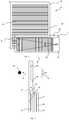
Figure 3 , there is shown awaveguide 40 formed from a substrate of material, comprising a firstinternal face 42 and a secondinternal face 44 parallely spaced from one another. Thewaveguide 40 is arranged to total internally reflect injected light along alight path 46 between the first andsecond faces light path 46, injected light is arranged to enter thewaveguide 40 at greater than the critical angle φc1 for the substrate of material from which thewaveguide 40 is formed, as measured from anormal axis 48 to thewaveguide 40. - A
grating element 50 carried within the layer of material of thewaveguide 60 is arranged such that impinging light following thelight path 46 is either diffracted out of thewaveguide 60 as a pupil ofimage bearing light 52a to 52c, for viewing by the observer, or the image bearing light passes through thegrating element 50 and is reflected by either the firstinternal face 42 or the secondinternal face 44 of thewaveguide 40 so as to propagate further along thewaveguide 40 towards adistal end 54. Accordingly, the light internally reflected within thewaveguide 40 will impinge on thegrating element 50 further along thelight path 46. - Referring to
Figure 4 , there is shown awaveguide 60 including a substrate ofmaterial 62, which has a firstinternal face 64 and a secondinternal face 66 parallely spaced from one another and arranged to allow propagation of image bearing light along a propagation axis to follow alight path 68 within the substrate ofmaterial 62 by total internal reflection of the image bearing light. The substrate ofmaterial 62 is a light transparent material arranged to allow an observer, not illustrated, to look through the substrate ofmaterial 62 whilst also arranged to carry image bearing light to provide a display image to the observer overlaid on a forward scene viewed through thewaveguide 60. - A
grating element 70 carried within the substrate ofmaterial 62 is arranged to interact with the light such that impinging image bearing light following thelight path 68 is either diffracted out of the substrate ofmaterial 62 as a pupil of image bearing light 72a to 72d for viewing by the observer, or the image bearing light passes through thegrating element 70 and is internally reflected by either the first or secondinternal face 70, 72 of the substrate ofmaterial 62 so as to propagate further along thelight path 68 towards adistal end 74. Accordingly, the image bearing light internally reflected within the substrate ofmaterial 62 will impinge on thegrating element 70 further along thelight path 68. - A first
external surface 76 of the substrate ofmaterial 62 is coated with anoptical layer 78 and a secondexternal surface 80 of the substrate ofmaterial 62 is coated with anoptical layer 82. The optical layers 80, 82 are arranged such that they reduce the critical angle φc2 required for total internal reflection of image bearing light within the substrate ofmaterial 62, as measured from anormal axis 84 to thewaveguide 60. The optical layers 78 and 82 can be formed from using a dielectric thin film coating. - Referring to
Figure 5 , which provides a comparison of the angle φ that image bearing light is injected into aprior art waveguide 40, as indicated byline 90, and injected into awaveguide 60 according to the present invention, as indicated by line 92, along theabscissa 94, against the light internally reflected within thewaveguides 40, 92, along theordinate 96. It will be observed from a comparison of the response curves for theprior art waveguide 40 and thewaveguide 60 of the present invention, lines 90 and 92, that theprior art waveguide 40 will provide a critical angle φc1 that is greater than the critical angle φc2 provided by thewaveguide 60 according to the present invention. - The difference between the two critical angles φc1 and φc2, indicated by
double arrow 98, provides thewaveguide 60 with an advantage of being able to be used for a greater angular range of injected image bearing light than theprior art waveguide 40. Furthermore, and as observed from a comparison ofFigures 3 and 4 , as the critical angle φc2 for injecting image bearing light has been reduced, the image bearing light will interact with thegrating element 70 more often than that of the prior art described with reference toFigure 3 . Accordingly, more pupils of image bearing light 72a to 72d will exit thewaveguide 60, thereby mitigating pupil banding as perceived by the observer. - Referring to
Figure 6 , a comparison of thelight path 100 as provided by the prior art waveguide and thelight path 102 as provide by the waveguide of the present invention indicates that light interacts with agrating element 104 more often as the critical angle for total internal reflection within awaveguide 106 decreases. - It will be understood that the injection of image bearing light into the
waveguide 60 can be via one or more reflective, transmissive or refractive optical elements. Furthermore, thegrating element 70 can be reflective, thereby being arranged on or near onesurface waveguide 60. - Such a
waveguide 60 can be used in a projection display, for displaying an image to an observer, such as that described with reference toFigures 1 and 2 to correct irregularity of the intensity of image bearing light from thefirst grating 24 of the first plate-like waveguide 14 and/or thethird grating 34 of the second plate-like waveguide 16. - Referring to
Figure 7 there is shown aprior art waveguide 110 compared to awaveguide 112 according to the present invention.Prior art waveguide 110 is formed from a layer ofmaterial 114, comprising a firstinternal face 116 and a secondinternal face 118 parallely spaced from one another. Thewaveguide 110 is arranged to total internally reflect injected light along alight path 120 between the first andsecond faces light path 120, injected light is arranged to enter thewaveguide 110 at greater than the critical angle φc3 for the layer ofmaterial 114 from which thewaveguide 110 is formed, as measured from a normal axis 122 to thewaveguide 110. - A
grating element 124 carried within the layer ofmaterial 114 of thewaveguide 110 is arranged such that impinging light following thelight path 120 is either diffracted out of thewaveguide 110 as a pupil of image bearing light, as previously described with reference toFigure 3 , for viewing by the observer, or the image bearing light passes through thegrating element 124 and is reflected by either the firstinternal face 116 or the secondinternal face 118 of thewaveguide 110 so as to propagate further along thewaveguide 110 towards adistal end 126. Accordingly, the light internally reflected within thewaveguide 110 will impinge on thegrating element 124 further along thelight path 120. - Light injected into the
waveguide 110 is arranged to impinge on anoptical element 128 arranged on or within the substrate ofmaterial 114 that is arranged to reflect the light such that it follows thelight path 120. The minimum angle for φc3 is dependent on the critical angle for the substrate ofmaterial 114. A maximum angle φc4, as measured from anormal axis 130 to thewaveguide 110, for light injected into thewaveguide 110 is dependent upon the desired interaction between light following thelight path 120 and thegrating element 124 and the period between pupils associated with light exiting thewaveguide 110, which in turn determines perceived pupil banding. Accordingly, the angles φc3 and φc4 determine the total field ofview 132 of the image transmitted by thewaveguide 110. - This is to be compared to the
waveguide 112 of the present invention, which includes a substrate ofmaterial 134, which has a firstinternal face 136 and a secondinternal face 138 parallely spaced from one another and arranged to allow propagation of image bearing light along a propagation axis to follow alight path 140 within the substrate ofmaterial 134 by total internal reflection of the image bearing light. The substrate ofmaterial 134 is a light transparent material arranged to allow an observer, not illustrated, to look through the substrate ofmaterial 134 whilst also arranged to carry image bearing light to provide a display image to the observer overlaid on a forward scene viewed through thewaveguide 112. - A
grating element 142 carried within the substrate ofmaterial 134 is arranged such that impinging image bearing light following thelight path 140 is either diffracted out of the substrate ofmaterial 134 as a pupil of image bearing light, as previously described with reference toFigure 4 , for viewing by the observer, or the image bearing light passes through thegrating element 142 and is internally reflected by either the first or secondinternal face material 134 so as to propagate further along thelight path 140 towards adistal end 144. Accordingly, the image bearing light internally reflected within the substrate ofmaterial 134 will impinge on thegrating element 142 further along thelight path 140. - A first
external surface 146 of the substrate ofmaterial 134 is coated with anoptical layer 148 and a secondexternal surface 150 of the substrate ofmaterial 134 is coated with anoptical layer 152. Theoptical layers material 134, as measured from anormal axis 154 to thewaveguide 112. Theoptical layers - Image bearing light injected into the
waveguide 112 is arranged to impinge on anoptical element 156 arranged on or within the substrate ofmaterial 134 that is arranged to reflect the image bearing light such that it follows thelight path 140. The minimum angle for φc5 is dependent on the critical angle for the substrate ofmaterial 134 as reduced by the addition ofoptical layers prior art waveguide 110, the maximum angle φc4, as measured from anormal axis 158 to thewaveguide 112, for light injected into thewaveguide 112 is dependent upon the desired interaction between image bearing light following thelight path 140 and thegrating element 142 and the period between pupils associated with image bearing light exiting thewaveguide 112, which in turn determines perceived pupil banding. Accordingly, the angles φc4 and φc5 determine the total field ofview 160 of the image transmitted by thewaveguide 112. - As will be noted from chained
lines double arrows view 160 ofwaveguide 112 is greater than the total field ofview 132 ofprior art waveguide 110. The increased total field ofview 160 is provided by the reduced critical angle φc5 provided byoptical layers - It will be understood that the injection of image bearing light into the
waveguide 112 can be via one or more reflective, transmissive or refractive optical elements. Furthermore, thegrating element 142 can be reflective, thereby being arranged on or near onesurface waveguide 112. - Such a
waveguide 112 can be used in a projection display, for displaying an image to an observer, such as that described with reference toFigures 1 and 2 to correct irregularity of the intensity of image bearing light from thefirst grating 24 of the first plate-like waveguide 14 and/or thethird grating 34 of the second plate-like waveguide 16 and/or to increase the field of view of such a projection display. - In a known waveguide according to the prior art, total internal reflection occurs when the angle of incidence of a light ray impinging on a parallel surface of the waveguide is above the critical angle. However, as shown in the graph of
Figure 8 , below the critical angle a small amount of reflection still occurs inangular region 160 at angles close to the normal axis. The reflection losses are due to Fresnel reflection in high refractive index waveguide material at the waveguide/air boundary, and reduce the amount of image bearing light which is received by a viewer. As shown diagrammatically inFigure 9 , Fresnel reflection losses at the waveguide/air boundary 166 occur both in the image bearing light 162 which is coupled out of the waveguide by the output diffraction grating and also in the light 164 transmitted through the waveguide, acting as a combiner, from an outside world scene. - In embodiments of the invention, a coating is applied to the surface of the or each waveguide to decrease the critical angle at which total internal reflection occurs in order to increase the number of interactions between image bearing light and an output diffraction grating over a unit length of the grating.
Figure 10 shows the reduction in the critical angle, which in this example is from about 33° to about 25°. In this regard, the image bearing light undergoing total internal reflection in the coated waveguide is indicated bynumeral 168, in both p and s polarisations, whereas the image bearing light undergoing total internal reflection in the prior art waveguide is indicated bynumeral 170. Accordingly, the coated waveguide can increase the number of interactions with the output grating. - Additionally, the coating, or optical layers, of the present embodiments are configured to reduce Fresnel reflection of image bearing light 166 and
outside world light 164 at angles close to the normal axis. In this regard, it will be seen inFigure 10 that at angles of incidence below the critical angle, which in this example is in therange 172 below about 25°, reflectance is decreased to zero or almost zero for both p and s polarised light. Accordingly, both the image generated by the display and the outside world light appears brighter through waveguide. - It will be appreciated that for example when such a display is used as a head up display a viewer will need to view an outside world scene through the waveguide over a range of angles including viewing along the normal axis and at about 25° to the normal in both elevation and azimuth. The see-through
angular range 174 is shown inFigure 11 over anangle 176 to thenormal axis 178. As shown inFigure 10 , the optical layer of the present embodiments provides reduced reflectance over a range of angles from 0° at the normal to about 25° at the outer limits of theangular range 174. Accordingly, the outside world scene appears brighter to a viewer across the full range of desired viewing. - Therefore, there are three requirements of the optical layers of the present embodiments. First, the critical angle of the waveguide is reduced to provide greater interactions of image bearing light with an output grating which in turn reduces exit pupil banding. Secondly, Fresnel reflections of the image bearing light output from the waveguide are reduced together with a reduction in reflections of the outside world scene. Thirdly, the light passing through the waveguide has reduced reflectance over a range of incidence angles allowing a viewer to view the outside world scene without reduced brightness.
- A suitable optical layer for the present embodiments is shown in
Figure 12 .Optical layer 180 is provided on a surface ofwaveguide 62 and comprises a plurality of layers. In this example, the optical layer comprises a stack of alternate layers of relatively low and relatively high refractive index material. As shown, the relatively high refractive index material layers 182, 184, 186 are made from the same material which may for example be TiO2 and the relatively low refractive index material layers 188, 190, 192 are made from the same material which may for example be MgF2. The multi-layer optical coating can be configured for optimising total internal reflection and reducing Fresnal reflections over the desired angular viewing range. Selection of coating parameters such as the number of layers, the type of dielectric material used, and thickness of each layer allows characteristics such as reflectivity to be modified. The alternating high and low index layers allows a reflection from each interface within the coating stack. The thickness of the layers is selected to produce constructive interference at angles below the critical angle of the waveguide thereby reducing the total critical angle. - Whilst
Figure 12 shows one suitable arrangement of an optical layer it will be apparent to those skilled in the art that other materials and configurations may be adopted for decreasing the critical angle of the waveguide. TheFigure 12 arrangement allows fine adjustments to be made to the optical properties of the optical layer permitting the critical angle to be selected according to requirements and for Fresnel reflection to be reduced thereby enhancing the brightness of the display. In the alternative however a single layer optical layer, which may be a thin dielectric coating, could be adopted having a refractive index which is less than the refractive index of the waveguide substrate and yet higher than the refractive index of air. Such an alternative arrangement causes refraction of the light passing through the waveguide substrate/optical layer boundary at an angle which is greater than the critical angle of the optical layer so that light undergoes total internal reflection in the optical layer and is refracted back into the waveguide substrate.
Claims (13)
- A waveguide for a projection display, including:a light transmissive substrate of material having two opposed substantially parallel faces, the substrate of material being arranged to transmit light within the substrate of material, between the parallel faces, under total internal reflection, the substrate of material having a given critical angle required for total internal reflection;an output grating element arranged within the substrate of material to diffract a portion of light incident thereon out of the substrate of material and to allow the remainder of the light to be transmitted within the substrate of material under total internal reflection; andan optical layer arranged on each of the parallel faces, the optical layer being arranged to reduce the given critical angle required for total internal reflection of light within the substrate of material so that the number of interactions between light transmitted within the substrate and the grating element can be increased.
- A waveguide, as claimed in Claim 1, comprising means for inputting light into the substrate at angles of incidence relative to the substantially parallel faces which are between a critical angle of the substrate without the optical layer and a reduced critical angle of the substrate with the optical layer.
- A waveguide, as claimed in Claim 1 or 2, wherein the optical layer is selected to reduce Fresnel reflectance of light at the faces of the substrate having an angle of incidence which is between the critical angle of the substrate with the optical layer and a normal axis when light is diffracted out of the substrate by the output grating element.
- A waveguide, as claimed in any of the preceding Claims, wherein the optical layer comprises a plurality of layers in which alternate layers have relatively high and relatively low refractive indices.
- A waveguide, as claimed in Claim 4, wherein the or each relatively high refractive index layer is made from TiO2 and/or the or each relatively low refractive index layer is made from MgF2.
- A projection display, for displaying an image to an observer, including:first and second waveguides as claimed in any preceding Claim;an image-providing light source device arranged to generate an image and to inject image bearing light into the first waveguide;a first said output grating element associated with the first waveguide arranged to direct the image bearing light internally along the first waveguide under total internal reflection and via which the image bearing light is outputted from the first waveguide, the first waveguide having a given critical angle required for total internal reflection;an input grating element arranged to receive the image bearing light from the first waveguide and to inject the image bearing light along the second waveguide under total internal reflection, the second waveguide having a given critical angle required for total internal reflection; anda second said output grating element arranged in the second waveguide to diffract received image bearing light out of the second waveguide towards an observer;wherein the optical layers of the first and second waveguides reduce the given critical angle required for total internal reflection of image bearing light within the waveguides to increase the number of interactions between the light propagating within the first waveguide and the first output grating element and between the light propagating within the second waveguide and the second output grating element.
- A projection display as claimed in Claim 6, wherein one or more of the grating elements are holographic optical elements or semi-reflective surfaces.
- A projection display, as claimed in Claims 6 or 7, wherein the first waveguide is plate-like, the second waveguide is plate-like and the first and second waveguides are arranged substantially parallel to one another.
- A projection display, as claimed in any of Claim 6 to 8, wherein the first waveguide and the second waveguide are arranged substantially in the same plane.
- A projection display, as claimed in Claim 8, wherein the first waveguide and the second waveguide are formed within a single piece of material.
- A projection display, as claimed in Claim 6 or 7, wherein the first waveguide is rod-like, the second waveguide is plate-like and the first and second waveguide are arranged such the image bearing light exits the first waveguide along a longitudinal axis of the first waveguide and enters the second waveguide to propagate along a propagation axis of the second waveguide.
- A head up display, or helmet mounted display, or head mounted display including a waveguide as claimed in any of Claims 1 to 5.
- A head up display, or helmet mounted display, or head mounted display including a projection display as claimed in any of Claims 6 to 11.
Priority Applications (1)
| Application Number | Priority Date | Filing Date | Title |
|---|---|---|---|
| EP09806027.0AEP2376971B1 (en) | 2008-12-12 | 2009-12-10 | Improvements in or relating to waveguides |
Applications Claiming Priority (4)
| Application Number | Priority Date | Filing Date | Title |
|---|---|---|---|
| GB0822684AGB0822684D0 (en) | 2008-12-12 | 2008-12-12 | Improvements in or relating to waveguides |
| EP08275085AEP2196842A1 (en) | 2008-12-12 | 2008-12-12 | Improvements in or relating to waveguides |
| PCT/GB2009/051682WO2010067117A1 (en) | 2008-12-12 | 2009-12-10 | Improvements in or relating to waveguides |
| EP09806027.0AEP2376971B1 (en) | 2008-12-12 | 2009-12-10 | Improvements in or relating to waveguides |
Publications (2)
| Publication Number | Publication Date |
|---|---|
| EP2376971A1 EP2376971A1 (en) | 2011-10-19 |
| EP2376971B1true EP2376971B1 (en) | 2019-02-20 |
Family
ID=42122966
Family Applications (1)
| Application Number | Title | Priority Date | Filing Date |
|---|---|---|---|
| EP09806027.0AActiveEP2376971B1 (en) | 2008-12-12 | 2009-12-10 | Improvements in or relating to waveguides |
Country Status (4)
| Country | Link |
|---|---|
| US (1) | US8654420B2 (en) |
| EP (1) | EP2376971B1 (en) |
| ES (1) | ES2717200T3 (en) |
| WO (1) | WO2010067117A1 (en) |
Cited By (1)
| Publication number | Priority date | Publication date | Assignee | Title |
|---|---|---|---|---|
| CN107111204A (en)* | 2014-09-29 | 2017-08-29 | 奇跃公司 | Architecture and method for outputting light of different wavelengths from a waveguide |
Families Citing this family (130)
| Publication number | Priority date | Publication date | Assignee | Title |
|---|---|---|---|---|
| GB0522968D0 (en) | 2005-11-11 | 2005-12-21 | Popovich Milan M | Holographic illumination device |
| GB0718706D0 (en) | 2007-09-25 | 2007-11-07 | Creative Physics Ltd | Method and apparatus for reducing laser speckle |
| US9335604B2 (en) | 2013-12-11 | 2016-05-10 | Milan Momcilo Popovich | Holographic waveguide display |
| US11726332B2 (en) | 2009-04-27 | 2023-08-15 | Digilens Inc. | Diffractive projection apparatus |
| US11300795B1 (en) | 2009-09-30 | 2022-04-12 | Digilens Inc. | Systems for and methods of using fold gratings coordinated with output couplers for dual axis expansion |
| US8233204B1 (en) | 2009-09-30 | 2012-07-31 | Rockwell Collins, Inc. | Optical displays |
| US10795160B1 (en) | 2014-09-25 | 2020-10-06 | Rockwell Collins, Inc. | Systems for and methods of using fold gratings for dual axis expansion |
| US11320571B2 (en)* | 2012-11-16 | 2022-05-03 | Rockwell Collins, Inc. | Transparent waveguide display providing upper and lower fields of view with uniform light extraction |
| US20200057353A1 (en) | 2009-10-09 | 2020-02-20 | Digilens Inc. | Compact Edge Illuminated Diffractive Display |
| US11204540B2 (en) | 2009-10-09 | 2021-12-21 | Digilens Inc. | Diffractive waveguide providing a retinal image |
| US8659826B1 (en) | 2010-02-04 | 2014-02-25 | Rockwell Collins, Inc. | Worn display system and method without requiring real time tracking for boresight precision |
| WO2012136970A1 (en) | 2011-04-07 | 2012-10-11 | Milan Momcilo Popovich | Laser despeckler based on angular diversity |
| EP2995986B1 (en) | 2011-08-24 | 2017-04-12 | Rockwell Collins, Inc. | Data display |
| WO2016020630A2 (en) | 2014-08-08 | 2016-02-11 | Milan Momcilo Popovich | Waveguide laser illuminator incorporating a despeckler |
| US10670876B2 (en) | 2011-08-24 | 2020-06-02 | Digilens Inc. | Waveguide laser illuminator incorporating a despeckler |
| US9507150B1 (en) | 2011-09-30 | 2016-11-29 | Rockwell Collins, Inc. | Head up display (HUD) using a bent waveguide assembly |
| US9715067B1 (en) | 2011-09-30 | 2017-07-25 | Rockwell Collins, Inc. | Ultra-compact HUD utilizing waveguide pupil expander with surface relief gratings in high refractive index materials |
| US8903207B1 (en)* | 2011-09-30 | 2014-12-02 | Rockwell Collins, Inc. | System for and method of extending vertical field of view in head up display utilizing a waveguide combiner |
| US9366864B1 (en) | 2011-09-30 | 2016-06-14 | Rockwell Collins, Inc. | System for and method of displaying information without need for a combiner alignment detector |
| US8634139B1 (en) | 2011-09-30 | 2014-01-21 | Rockwell Collins, Inc. | System for and method of catadioptric collimation in a compact head up display (HUD) |
| US8937772B1 (en) | 2011-09-30 | 2015-01-20 | Rockwell Collins, Inc. | System for and method of stowing HUD combiners |
| BR112014012615A2 (en) | 2011-11-23 | 2017-06-13 | Magic Leap Inc | three-dimensional augmented reality and virtual reality display system |
| US20150010265A1 (en) | 2012-01-06 | 2015-01-08 | Milan, Momcilo POPOVICH | Contact image sensor using switchable bragg gratings |
| US9052414B2 (en) | 2012-02-07 | 2015-06-09 | Microsoft Technology Licensing, Llc | Virtual image device |
| US9354748B2 (en) | 2012-02-13 | 2016-05-31 | Microsoft Technology Licensing, Llc | Optical stylus interaction |
| US8749529B2 (en) | 2012-03-01 | 2014-06-10 | Microsoft Corporation | Sensor-in-pixel display system with near infrared filter |
| US9460029B2 (en) | 2012-03-02 | 2016-10-04 | Microsoft Technology Licensing, Llc | Pressure sensitive keys |
| US9870066B2 (en) | 2012-03-02 | 2018-01-16 | Microsoft Technology Licensing, Llc | Method of manufacturing an input device |
| US8873227B2 (en) | 2012-03-02 | 2014-10-28 | Microsoft Corporation | Flexible hinge support layer |
| US9075566B2 (en) | 2012-03-02 | 2015-07-07 | Microsoft Technoogy Licensing, LLC | Flexible hinge spine |
| US9298236B2 (en) | 2012-03-02 | 2016-03-29 | Microsoft Technology Licensing, Llc | Multi-stage power adapter configured to provide a first power level upon initial connection of the power adapter to the host device and a second power level thereafter upon notification from the host device to the power adapter |
| US9274338B2 (en) | 2012-03-21 | 2016-03-01 | Microsoft Technology Licensing, Llc | Increasing field of view of reflective waveguide |
| US9523852B1 (en) | 2012-03-28 | 2016-12-20 | Rockwell Collins, Inc. | Micro collimator system and method for a head up display (HUD) |
| CN106125308B (en) | 2012-04-25 | 2019-10-25 | 罗克韦尔柯林斯公司 | Device and method for displaying images |
| WO2013167864A1 (en) | 2012-05-11 | 2013-11-14 | Milan Momcilo Popovich | Apparatus for eye tracking |
| US20130300590A1 (en) | 2012-05-14 | 2013-11-14 | Paul Henry Dietz | Audio Feedback |
| US10031556B2 (en) | 2012-06-08 | 2018-07-24 | Microsoft Technology Licensing, Llc | User experience adaptation |
| US9019615B2 (en) | 2012-06-12 | 2015-04-28 | Microsoft Technology Licensing, Llc | Wide field-of-view virtual image projector |
| US9355345B2 (en) | 2012-07-23 | 2016-05-31 | Microsoft Technology Licensing, Llc | Transparent tags with encoded data |
| US8964379B2 (en) | 2012-08-20 | 2015-02-24 | Microsoft Corporation | Switchable magnetic lock |
| US9152173B2 (en) | 2012-10-09 | 2015-10-06 | Microsoft Technology Licensing, Llc | Transparent display device |
| US9933684B2 (en) | 2012-11-16 | 2018-04-03 | Rockwell Collins, Inc. | Transparent waveguide display providing upper and lower fields of view having a specific light output aperture configuration |
| FR2999301B1 (en)* | 2012-12-12 | 2015-01-09 | Thales Sa | OPTICAL GUIDE OF COLLIMATE IMAGES WITH OPTICAL BEAM DEDOLDER AND OPTICAL DEVICE THEREFOR |
| US9513748B2 (en) | 2012-12-13 | 2016-12-06 | Microsoft Technology Licensing, Llc | Combined display panel circuit |
| US9638835B2 (en) | 2013-03-05 | 2017-05-02 | Microsoft Technology Licensing, Llc | Asymmetric aberration correcting lens |
| US9674413B1 (en) | 2013-04-17 | 2017-06-06 | Rockwell Collins, Inc. | Vision system and method having improved performance and solar mitigation |
| US10209517B2 (en) | 2013-05-20 | 2019-02-19 | Digilens, Inc. | Holographic waveguide eye tracker |
| US8913865B1 (en) | 2013-06-27 | 2014-12-16 | Microsoft Corporation | Waveguide including light turning gaps |
| WO2015015138A1 (en) | 2013-07-31 | 2015-02-05 | Milan Momcilo Popovich | Method and apparatus for contact image sensing |
| US9244281B1 (en) | 2013-09-26 | 2016-01-26 | Rockwell Collins, Inc. | Display system and method using a detached combiner |
| FR3014209B1 (en)* | 2013-11-29 | 2017-03-03 | Commissariat Energie Atomique | OUTPUT PUPIL EXTENSION DEVICE AND HIGH HEAD VIEWER HAVING THE DEVICE |
| US10732407B1 (en) | 2014-01-10 | 2020-08-04 | Rockwell Collins, Inc. | Near eye head up display system and method with fixed combiner |
| US9519089B1 (en) | 2014-01-30 | 2016-12-13 | Rockwell Collins, Inc. | High performance volume phase gratings |
| US10120420B2 (en) | 2014-03-21 | 2018-11-06 | Microsoft Technology Licensing, Llc | Lockable display and techniques enabling use of lockable displays |
| US9244280B1 (en) | 2014-03-25 | 2016-01-26 | Rockwell Collins, Inc. | Near eye display system and method for display enhancement or redundancy |
| RU2603238C2 (en) | 2014-07-15 | 2016-11-27 | Самсунг Электроникс Ко., Лтд. | Light-guide structure, holographic optical device and imaging system |
| US10324733B2 (en) | 2014-07-30 | 2019-06-18 | Microsoft Technology Licensing, Llc | Shutdown notifications |
| US10254942B2 (en) | 2014-07-31 | 2019-04-09 | Microsoft Technology Licensing, Llc | Adaptive sizing and positioning of application windows |
| US10592080B2 (en) | 2014-07-31 | 2020-03-17 | Microsoft Technology Licensing, Llc | Assisted presentation of application windows |
| US10678412B2 (en) | 2014-07-31 | 2020-06-09 | Microsoft Technology Licensing, Llc | Dynamic joint dividers for application windows |
| US10359736B2 (en) | 2014-08-08 | 2019-07-23 | Digilens Inc. | Method for holographic mastering and replication |
| WO2016042283A1 (en) | 2014-09-19 | 2016-03-24 | Milan Momcilo Popovich | Method and apparatus for generating input images for holographic waveguide displays |
| US9715110B1 (en) | 2014-09-25 | 2017-07-25 | Rockwell Collins, Inc. | Automotive head up display (HUD) |
| US10088675B1 (en) | 2015-05-18 | 2018-10-02 | Rockwell Collins, Inc. | Turning light pipe for a pupil expansion system and method |
| EP3198192A1 (en) | 2014-09-26 | 2017-08-02 | Milan Momcilo Popovich | Holographic waveguide opticaltracker |
| IL235642B (en)* | 2014-11-11 | 2021-08-31 | Lumus Ltd | Compact head-mounted display system protected by a hyperfine structure |
| IL236490B (en)* | 2014-12-25 | 2021-10-31 | Lumus Ltd | Optical component on a conductive substrate |
| US20180275402A1 (en) | 2015-01-12 | 2018-09-27 | Digilens, Inc. | Holographic waveguide light field displays |
| WO2016113534A1 (en) | 2015-01-12 | 2016-07-21 | Milan Momcilo Popovich | Environmentally isolated waveguide display |
| EP3248026B1 (en) | 2015-01-20 | 2019-09-04 | DigiLens Inc. | Holographic waveguide lidar |
| US11086216B2 (en) | 2015-02-09 | 2021-08-10 | Microsoft Technology Licensing, Llc | Generating electronic components |
| US10018844B2 (en) | 2015-02-09 | 2018-07-10 | Microsoft Technology Licensing, Llc | Wearable image display system |
| US9827209B2 (en) | 2015-02-09 | 2017-11-28 | Microsoft Technology Licensing, Llc | Display system |
| US10317677B2 (en) | 2015-02-09 | 2019-06-11 | Microsoft Technology Licensing, Llc | Display system |
| US9632226B2 (en) | 2015-02-12 | 2017-04-25 | Digilens Inc. | Waveguide grating device |
| WO2016146963A1 (en) | 2015-03-16 | 2016-09-22 | Popovich, Milan, Momcilo | Waveguide device incorporating a light pipe |
| WO2016156776A1 (en) | 2015-03-31 | 2016-10-06 | Milan Momcilo Popovich | Method and apparatus for contact image sensing |
| US10126552B2 (en) | 2015-05-18 | 2018-11-13 | Rockwell Collins, Inc. | Micro collimator system and method for a head up display (HUD) |
| US10247943B1 (en) | 2015-05-18 | 2019-04-02 | Rockwell Collins, Inc. | Head up display (HUD) using a light pipe |
| US11366316B2 (en) | 2015-05-18 | 2022-06-21 | Rockwell Collins, Inc. | Head up display (HUD) using a light pipe |
| US10108010B2 (en) | 2015-06-29 | 2018-10-23 | Rockwell Collins, Inc. | System for and method of integrating head up displays and head down displays |
| CN113759555B (en) | 2015-10-05 | 2024-09-20 | 迪吉伦斯公司 | Waveguide Display |
| US10598932B1 (en) | 2016-01-06 | 2020-03-24 | Rockwell Collins, Inc. | Head up display for integrating views of conformally mapped symbols and a fixed image source |
| NZ743884A (en)* | 2016-01-07 | 2019-11-29 | Magic Leap Inc | Virtual and augmented reality systems and methods having unequal numbers of component color images distributed across depth planes |
| JP6825275B2 (en)* | 2016-01-21 | 2021-02-03 | 株式会社リコー | Virtual image display device |
| CN109073889B (en) | 2016-02-04 | 2021-04-27 | 迪吉伦斯公司 | Holographic waveguide optical tracker |
| CN108780224B (en) | 2016-03-24 | 2021-08-03 | 迪吉伦斯公司 | Method and apparatus for providing a polarization selective holographic waveguide device |
| US10890707B2 (en) | 2016-04-11 | 2021-01-12 | Digilens Inc. | Holographic waveguide apparatus for structured light projection |
| US10067347B2 (en) | 2016-04-13 | 2018-09-04 | Microsoft Technology Licensing, Llc | Waveguides with improved intensity distributions |
| US9791703B1 (en) | 2016-04-13 | 2017-10-17 | Microsoft Technology Licensing, Llc | Waveguides with extended field of view |
| US10061124B2 (en) | 2016-04-29 | 2018-08-28 | Microsoft Technology Licensing, Llc | Robust architecture for large field of view components |
| AU2017264780B2 (en) | 2016-05-12 | 2022-05-12 | Magic Leap, Inc. | Distributed light manipulation over imaging waveguide |
| US10353202B2 (en)* | 2016-06-09 | 2019-07-16 | Microsoft Technology Licensing, Llc | Wrapped waveguide with large field of view |
| CN107632406A (en)* | 2016-07-18 | 2018-01-26 | 北京灵犀微光科技有限公司 | Holographic waveguide, augmented reality display system and display method |
| US10095045B2 (en) | 2016-09-12 | 2018-10-09 | Microsoft Technology Licensing, Llc | Waveguide comprising a bragg polarization grating |
| EP3542213B1 (en)* | 2016-11-18 | 2025-10-08 | Magic Leap, Inc. | Waveguide light multiplexer using crossed gratings |
| WO2018102834A2 (en)* | 2016-12-02 | 2018-06-07 | Digilens, Inc. | Waveguide device with uniform output illumination |
| US10545346B2 (en) | 2017-01-05 | 2020-01-28 | Digilens Inc. | Wearable heads up displays |
| US10295824B2 (en) | 2017-01-26 | 2019-05-21 | Rockwell Collins, Inc. | Head up display with an angled light pipe |
| WO2018150163A1 (en)* | 2017-02-14 | 2018-08-23 | Bae Systems Plc | Waveguide structure |
| FI129873B (en) | 2017-05-08 | 2022-10-14 | Dispelix Oy | Diffractive display, lightguide element and projector therefor, and method for displaying image |
| US10175423B2 (en) | 2017-05-31 | 2019-01-08 | Microsoft Technology Licensing, Llc | Optical waveguide using overlapping optical elements |
| US11131807B2 (en) | 2017-05-31 | 2021-09-28 | Microsoft Technology Licensing, Llc | Pupil expander with improved color uniformity |
| WO2019079350A2 (en) | 2017-10-16 | 2019-04-25 | Digilens, Inc. | Systems and methods for multiplying the image resolution of a pixelated display |
| EP3710876A4 (en) | 2018-01-08 | 2022-02-09 | DigiLens Inc. | SYSTEMS AND METHODS OF FABRICATING WAVEGUIDE CELLS |
| WO2019136476A1 (en) | 2018-01-08 | 2019-07-11 | Digilens, Inc. | Waveguide architectures and related methods of manufacturing |
| US10732569B2 (en) | 2018-01-08 | 2020-08-04 | Digilens Inc. | Systems and methods for high-throughput recording of holographic gratings in waveguide cells |
| EP3710894B1 (en) | 2018-01-08 | 2025-07-30 | Digilens Inc. | Methods for fabricating optical waveguides |
| US10690851B2 (en) | 2018-03-16 | 2020-06-23 | Digilens Inc. | Holographic waveguides incorporating birefringence control and methods for their fabrication |
| US10761256B2 (en)* | 2018-04-16 | 2020-09-01 | Samsung Electronics Co., Ltd. | Backlight unit providing uniform light and display apparatus including the same |
| RU2673013C1 (en)* | 2018-04-16 | 2018-11-21 | Самсунг Электроникс Ко., Лтд. | Coherent lighting device with light recuperation |
| DE102018211747B4 (en)* | 2018-07-13 | 2021-02-25 | Audi Ag | Display device for a motor vehicle, method for generating a virtual representation of optical image information, and motor vehicle |
| WO2020023779A1 (en) | 2018-07-25 | 2020-01-30 | Digilens Inc. | Systems and methods for fabricating a multilayer optical structure |
| WO2020019809A1 (en) | 2018-07-26 | 2020-01-30 | Boe Technology Group Co., Ltd. | Microfluidic apparatus, method of detecting substance in microfluidic apparatus, and spectrometer |
| CN110764186B (en) | 2018-07-27 | 2022-02-22 | 京东方科技集团股份有限公司 | Optical waveguide substrate and microfluidic device |
| US20200225471A1 (en) | 2019-01-14 | 2020-07-16 | Digilens Inc. | Holographic Waveguide Display with Light Control Layer |
| US20200247017A1 (en) | 2019-02-05 | 2020-08-06 | Digilens Inc. | Methods for Compensating for Optical Surface Nonuniformity |
| KR102866596B1 (en) | 2019-02-15 | 2025-09-29 | 디지렌즈 인코포레이티드. | Method and device for providing a holographic waveguide display using an integral grating |
| US20220283377A1 (en) | 2019-02-15 | 2022-09-08 | Digilens Inc. | Wide Angle Waveguide Display |
| WO2020186113A1 (en) | 2019-03-12 | 2020-09-17 | Digilens Inc. | Holographic waveguide backlight and related methods of manufacturing |
| JP7259461B2 (en)* | 2019-03-25 | 2023-04-18 | セイコーエプソン株式会社 | Display device |
| EP3980825A4 (en)* | 2019-06-07 | 2023-05-03 | Digilens Inc. | WAVEGUIDES WITH TRANSMITTING AND REFLECTING GRIDS AND RELATED MANUFACTURING PROCESSES |
| EP4004646A4 (en) | 2019-07-29 | 2023-09-06 | Digilens Inc. | METHODS AND APPARATUS FOR MULTIPLYING THE IMAGE RESOLUTION AND FIELD OF VIEW OF A PIXELATED DISPLAY SCREEN |
| KR102775783B1 (en) | 2019-08-29 | 2025-02-28 | 디지렌즈 인코포레이티드. | Vacuum grid and method for manufacturing the same |
| CN110989182A (en)* | 2019-11-29 | 2020-04-10 | 中国科学院长春光学精密机械与物理研究所 | Beam combination light source device |
| JP7424396B2 (en)* | 2020-02-07 | 2024-01-30 | 株式会社島津製作所 | Display device and optical element used in the display device |
| JP2024502255A (en) | 2020-12-21 | 2024-01-18 | ディジレンズ インコーポレイテッド | Eye glow suppression in waveguide-based displays |
| WO2022150841A1 (en) | 2021-01-07 | 2022-07-14 | Digilens Inc. | Grating structures for color waveguides |
| US12158612B2 (en) | 2021-03-05 | 2024-12-03 | Digilens Inc. | Evacuated periodic structures and methods of manufacturing |
| US11874463B2 (en)* | 2021-08-04 | 2024-01-16 | Himax Technologies Limited | Waveguide combiner with at least one embedded film layer |
Family Cites Families (18)
| Publication number | Priority date | Publication date | Assignee | Title |
|---|---|---|---|---|
| US3806223A (en) | 1972-03-30 | 1974-04-23 | Corning Glass Works | Planar optical waveguide |
| DE3266408D1 (en) | 1981-10-14 | 1985-10-24 | Gec Avionics | Optical arrangements for head-up displays and night vision goggles |
| US6139176A (en)* | 1998-07-02 | 2000-10-31 | Federal-Mogul World Wide, Inc. | Optical waveguide structure with raised or embedded waveguides |
| US20030063042A1 (en) | 1999-07-29 | 2003-04-03 | Asher A. Friesem | Electronic utility devices incorporating a compact virtual image display |
| US6685325B1 (en)* | 1999-10-21 | 2004-02-03 | Federal-Mogul World Wide, Inc. | Vehicle side mirror assembly with integral illumination and signal lighting |
| AU2001282899A1 (en) | 2000-07-21 | 2002-02-05 | Motorola, Inc. | Monolithic optical system |
| GB2402936B (en)* | 2000-12-20 | 2005-07-13 | Murata Manufacturing Co | Translucent ceramic,method of producing the same and optical devices |
| JP2002258081A (en)* | 2001-02-28 | 2002-09-11 | Fujitsu Ltd | Optical wiring board, method for manufacturing optical wiring board, and multilayer optical wiring |
| US6922872B2 (en) | 2001-08-02 | 2005-08-02 | Multimatic, Inc. | Automotive door hinge with structurally integrated pivot |
| IL148804A (en)* | 2002-03-21 | 2007-02-11 | Yaacov Amitai | Optical device |
| KR20030088217A (en) | 2002-05-13 | 2003-11-19 | 삼성전자주식회사 | Wearable display system enabling adjustment of magnfication |
| US7037952B2 (en) | 2002-08-02 | 2006-05-02 | Seiren Co., Ltd. | Ultraviolet ray curable ink, ink composition for ink jet and process for preparing ink jet printed matter using the same |
| US6832037B2 (en)* | 2002-08-09 | 2004-12-14 | Eastman Kodak Company | Waveguide and method of making same |
| US7205960B2 (en)* | 2003-02-19 | 2007-04-17 | Mirage Innovations Ltd. | Chromatic planar optic display system |
| US7016587B2 (en)* | 2004-01-20 | 2006-03-21 | Xerox Corporation | Low loss silicon waveguide and method of fabrication thereof |
| ATE520046T1 (en) | 2004-04-23 | 2011-08-15 | Olivier M Parriaux | HIGHLY EFFICIENT OPTICAL DIFFRACTION DEVICE |
| DE602006010215D1 (en) | 2005-09-07 | 2009-12-17 | Bae Systems Plc | PROJECTION DISPLAY WITH A STABLE WAVEGUIDE WITH RECTANGULAR CROSS-SECTION AND A PLATE-BASED WAVEGUIDE, WHICH HAVE EACH MOUNTING GRILLE |
| US9081178B2 (en) | 2005-09-07 | 2015-07-14 | Bae Systems Plc | Projection display for displaying an image to a viewer |
- 2009
- 2009-12-10EPEP09806027.0Apatent/EP2376971B1/enactiveActive
- 2009-12-10WOPCT/GB2009/051682patent/WO2010067117A1/enactiveApplication Filing
- 2009-12-10USUS13/133,628patent/US8654420B2/enactiveActive
- 2009-12-10ESES09806027Tpatent/ES2717200T3/enactiveActive
Non-Patent Citations (1)
| Title |
|---|
| None* |
Cited By (2)
| Publication number | Priority date | Publication date | Assignee | Title |
|---|---|---|---|---|
| CN107111204A (en)* | 2014-09-29 | 2017-08-29 | 奇跃公司 | Architecture and method for outputting light of different wavelengths from a waveguide |
| CN107111204B (en)* | 2014-09-29 | 2021-02-09 | 奇跃公司 | Architecture and method for outputting light of different wavelengths from a waveguide |
Also Published As
| Publication number | Publication date |
|---|---|
| US20110242670A1 (en) | 2011-10-06 |
| WO2010067117A1 (en) | 2010-06-17 |
| US8654420B2 (en) | 2014-02-18 |
| ES2717200T3 (en) | 2019-06-19 |
| EP2376971A1 (en) | 2011-10-19 |
Similar Documents
| Publication | Publication Date | Title |
|---|---|---|
| EP2376971B1 (en) | Improvements in or relating to waveguides | |
| EP2269111B1 (en) | Improvements in or relating to waveguides | |
| EP2110701A1 (en) | Improvements in or relating to waveguides | |
| US11846777B2 (en) | Interference-free waveguide display | |
| US8493662B2 (en) | Waveguides | |
| EP2979126B1 (en) | Improvements in and relating to displays | |
| US8107780B2 (en) | Display projectors | |
| CN104536088B (en) | Tooth form inlays planar waveguide optical device | |
| US20110235179A1 (en) | waveguides | |
| US20110242661A1 (en) | waveguides | |
| US20100246003A1 (en) | projection displays | |
| GB2514658A (en) | Improvements in and relating to displays | |
| WO2013043252A1 (en) | Lightweight eyepiece for head mounted display | |
| EP2196843A1 (en) | Improvements in or relating to waveguides | |
| CN119270419B (en) | Diffraction waveguide structure and near-to-eye display device | |
| US20240264354A1 (en) | Dual diffraction grating in-coupler for reduced waveguide thickness background | |
| EP2196842A1 (en) | Improvements in or relating to waveguides | |
| WO2023220133A1 (en) | Dual index waveguide stack | |
| EP4381227A1 (en) | Imaging light guide apparatus with light security | |
| WO2024211863A1 (en) | Image light guide with metalized diffractive elements | |
| CN118234993A (en) | Photosafe imaging light guide device |
Legal Events
| Date | Code | Title | Description |
|---|---|---|---|
| PUAI | Public reference made under article 153(3) epc to a published international application that has entered the european phase | Free format text:ORIGINAL CODE: 0009012 | |
| 17P | Request for examination filed | Effective date:20110712 | |
| AK | Designated contracting states | Kind code of ref document:A1 Designated state(s):AT BE BG CH CY CZ DE DK EE ES FI FR GB GR HR HU IE IS IT LI LT LU LV MC MK MT NL NO PL PT RO SE SI SK SM TR | |
| DAX | Request for extension of the european patent (deleted) | ||
| REG | Reference to a national code | Ref country code:DE Ref legal event code:R079 Ref document number:602009057092 Country of ref document:DE Free format text:PREVIOUS MAIN CLASS: G02B0027010000 Ipc:G02B0006000000 | |
| RIC1 | Information provided on ipc code assigned before grant | Ipc:G02B 27/01 20060101ALI20180626BHEP Ipc:G02B 6/00 20060101AFI20180626BHEP Ipc:F21V 8/00 20060101ALI20180626BHEP | |
| GRAP | Despatch of communication of intention to grant a patent | Free format text:ORIGINAL CODE: EPIDOSNIGR1 | |
| STAA | Information on the status of an ep patent application or granted ep patent | Free format text:STATUS: GRANT OF PATENT IS INTENDED | |
| INTG | Intention to grant announced | Effective date:20180906 | |
| GRAS | Grant fee paid | Free format text:ORIGINAL CODE: EPIDOSNIGR3 | |
| GRAA | (expected) grant | Free format text:ORIGINAL CODE: 0009210 | |
| STAA | Information on the status of an ep patent application or granted ep patent | Free format text:STATUS: THE PATENT HAS BEEN GRANTED | |
| AK | Designated contracting states | Kind code of ref document:B1 Designated state(s):AT BE BG CH CY CZ DE DK EE ES FI FR GB GR HR HU IE IS IT LI LT LU LV MC MK MT NL NO PL PT RO SE SI SK SM TR | |
| REG | Reference to a national code | Ref country code:GB Ref legal event code:FG4D | |
| REG | Reference to a national code | Ref country code:CH Ref legal event code:EP | |
| REG | Reference to a national code | Ref country code:DE Ref legal event code:R096 Ref document number:602009057092 Country of ref document:DE | |
| REG | Reference to a national code | Ref country code:AT Ref legal event code:REF Ref document number:1098958 Country of ref document:AT Kind code of ref document:T Effective date:20190315 | |
| REG | Reference to a national code | Ref country code:IE Ref legal event code:FG4D | |
| REG | Reference to a national code | Ref country code:ES Ref legal event code:FG2A Ref document number:2717200 Country of ref document:ES Kind code of ref document:T3 Effective date:20190619 | |
| REG | Reference to a national code | Ref country code:LT Ref legal event code:MG4D | |
| REG | Reference to a national code | Ref country code:NL Ref legal event code:MP Effective date:20190220 | |
| PG25 | Lapsed in a contracting state [announced via postgrant information from national office to epo] | Ref country code:LT Free format text:LAPSE BECAUSE OF FAILURE TO SUBMIT A TRANSLATION OF THE DESCRIPTION OR TO PAY THE FEE WITHIN THE PRESCRIBED TIME-LIMIT Effective date:20190220 Ref country code:FI Free format text:LAPSE BECAUSE OF FAILURE TO SUBMIT A TRANSLATION OF THE DESCRIPTION OR TO PAY THE FEE WITHIN THE PRESCRIBED TIME-LIMIT Effective date:20190220 Ref country code:PT Free format text:LAPSE BECAUSE OF FAILURE TO SUBMIT A TRANSLATION OF THE DESCRIPTION OR TO PAY THE FEE WITHIN THE PRESCRIBED TIME-LIMIT Effective date:20190620 Ref country code:NO Free format text:LAPSE BECAUSE OF FAILURE TO SUBMIT A TRANSLATION OF THE DESCRIPTION OR TO PAY THE FEE WITHIN THE PRESCRIBED TIME-LIMIT Effective date:20190520 Ref country code:SE Free format text:LAPSE BECAUSE OF FAILURE TO SUBMIT A TRANSLATION OF THE DESCRIPTION OR TO PAY THE FEE WITHIN THE PRESCRIBED TIME-LIMIT Effective date:20190220 | |
| PG25 | Lapsed in a contracting state [announced via postgrant information from national office to epo] | Ref country code:HR Free format text:LAPSE BECAUSE OF FAILURE TO SUBMIT A TRANSLATION OF THE DESCRIPTION OR TO PAY THE FEE WITHIN THE PRESCRIBED TIME-LIMIT Effective date:20190220 Ref country code:LV Free format text:LAPSE BECAUSE OF FAILURE TO SUBMIT A TRANSLATION OF THE DESCRIPTION OR TO PAY THE FEE WITHIN THE PRESCRIBED TIME-LIMIT Effective date:20190220 Ref country code:GR Free format text:LAPSE BECAUSE OF FAILURE TO SUBMIT A TRANSLATION OF THE DESCRIPTION OR TO PAY THE FEE WITHIN THE PRESCRIBED TIME-LIMIT Effective date:20190521 Ref country code:IS Free format text:LAPSE BECAUSE OF FAILURE TO SUBMIT A TRANSLATION OF THE DESCRIPTION OR TO PAY THE FEE WITHIN THE PRESCRIBED TIME-LIMIT Effective date:20190620 Ref country code:BG Free format text:LAPSE BECAUSE OF FAILURE TO SUBMIT A TRANSLATION OF THE DESCRIPTION OR TO PAY THE FEE WITHIN THE PRESCRIBED TIME-LIMIT Effective date:20190520 Ref country code:NL Free format text:LAPSE BECAUSE OF FAILURE TO SUBMIT A TRANSLATION OF THE DESCRIPTION OR TO PAY THE FEE WITHIN THE PRESCRIBED TIME-LIMIT Effective date:20190220 | |
| REG | Reference to a national code | Ref country code:AT Ref legal event code:MK05 Ref document number:1098958 Country of ref document:AT Kind code of ref document:T Effective date:20190220 | |
| PG25 | Lapsed in a contracting state [announced via postgrant information from national office to epo] | Ref country code:SK Free format text:LAPSE BECAUSE OF FAILURE TO SUBMIT A TRANSLATION OF THE DESCRIPTION OR TO PAY THE FEE WITHIN THE PRESCRIBED TIME-LIMIT Effective date:20190220 Ref country code:EE Free format text:LAPSE BECAUSE OF FAILURE TO SUBMIT A TRANSLATION OF THE DESCRIPTION OR TO PAY THE FEE WITHIN THE PRESCRIBED TIME-LIMIT Effective date:20190220 Ref country code:CZ Free format text:LAPSE BECAUSE OF FAILURE TO SUBMIT A TRANSLATION OF THE DESCRIPTION OR TO PAY THE FEE WITHIN THE PRESCRIBED TIME-LIMIT Effective date:20190220 Ref country code:RO Free format text:LAPSE BECAUSE OF FAILURE TO SUBMIT A TRANSLATION OF THE DESCRIPTION OR TO PAY THE FEE WITHIN THE PRESCRIBED TIME-LIMIT Effective date:20190220 Ref country code:DK Free format text:LAPSE BECAUSE OF FAILURE TO SUBMIT A TRANSLATION OF THE DESCRIPTION OR TO PAY THE FEE WITHIN THE PRESCRIBED TIME-LIMIT Effective date:20190220 | |
| REG | Reference to a national code | Ref country code:DE Ref legal event code:R097 Ref document number:602009057092 Country of ref document:DE | |
| PG25 | Lapsed in a contracting state [announced via postgrant information from national office to epo] | Ref country code:PL Free format text:LAPSE BECAUSE OF FAILURE TO SUBMIT A TRANSLATION OF THE DESCRIPTION OR TO PAY THE FEE WITHIN THE PRESCRIBED TIME-LIMIT Effective date:20190220 Ref country code:SM Free format text:LAPSE BECAUSE OF FAILURE TO SUBMIT A TRANSLATION OF THE DESCRIPTION OR TO PAY THE FEE WITHIN THE PRESCRIBED TIME-LIMIT Effective date:20190220 | |
| PLBE | No opposition filed within time limit | Free format text:ORIGINAL CODE: 0009261 | |
| STAA | Information on the status of an ep patent application or granted ep patent | Free format text:STATUS: NO OPPOSITION FILED WITHIN TIME LIMIT | |
| PG25 | Lapsed in a contracting state [announced via postgrant information from national office to epo] | Ref country code:AT Free format text:LAPSE BECAUSE OF FAILURE TO SUBMIT A TRANSLATION OF THE DESCRIPTION OR TO PAY THE FEE WITHIN THE PRESCRIBED TIME-LIMIT Effective date:20190220 | |
| 26N | No opposition filed | Effective date:20191121 | |
| PG25 | Lapsed in a contracting state [announced via postgrant information from national office to epo] | Ref country code:SI Free format text:LAPSE BECAUSE OF FAILURE TO SUBMIT A TRANSLATION OF THE DESCRIPTION OR TO PAY THE FEE WITHIN THE PRESCRIBED TIME-LIMIT Effective date:20190220 | |
| PG25 | Lapsed in a contracting state [announced via postgrant information from national office to epo] | Ref country code:TR Free format text:LAPSE BECAUSE OF FAILURE TO SUBMIT A TRANSLATION OF THE DESCRIPTION OR TO PAY THE FEE WITHIN THE PRESCRIBED TIME-LIMIT Effective date:20190220 | |
| REG | Reference to a national code | Ref country code:CH Ref legal event code:PL | |
| REG | Reference to a national code | Ref country code:BE Ref legal event code:MM Effective date:20191231 | |
| PG25 | Lapsed in a contracting state [announced via postgrant information from national office to epo] | Ref country code:MC Free format text:LAPSE BECAUSE OF FAILURE TO SUBMIT A TRANSLATION OF THE DESCRIPTION OR TO PAY THE FEE WITHIN THE PRESCRIBED TIME-LIMIT Effective date:20190220 | |
| PG25 | Lapsed in a contracting state [announced via postgrant information from national office to epo] | Ref country code:IE Free format text:LAPSE BECAUSE OF NON-PAYMENT OF DUE FEES Effective date:20191210 Ref country code:LU Free format text:LAPSE BECAUSE OF NON-PAYMENT OF DUE FEES Effective date:20191210 | |
| PG25 | Lapsed in a contracting state [announced via postgrant information from national office to epo] | Ref country code:LI Free format text:LAPSE BECAUSE OF NON-PAYMENT OF DUE FEES Effective date:20191231 Ref country code:BE Free format text:LAPSE BECAUSE OF NON-PAYMENT OF DUE FEES Effective date:20191231 Ref country code:CH Free format text:LAPSE BECAUSE OF NON-PAYMENT OF DUE FEES Effective date:20191231 | |
| PG25 | Lapsed in a contracting state [announced via postgrant information from national office to epo] | Ref country code:CY Free format text:LAPSE BECAUSE OF FAILURE TO SUBMIT A TRANSLATION OF THE DESCRIPTION OR TO PAY THE FEE WITHIN THE PRESCRIBED TIME-LIMIT Effective date:20190220 | |
| PG25 | Lapsed in a contracting state [announced via postgrant information from national office to epo] | Ref country code:HU Free format text:LAPSE BECAUSE OF FAILURE TO SUBMIT A TRANSLATION OF THE DESCRIPTION OR TO PAY THE FEE WITHIN THE PRESCRIBED TIME-LIMIT; INVALID AB INITIO Effective date:20091210 Ref country code:MT Free format text:LAPSE BECAUSE OF FAILURE TO SUBMIT A TRANSLATION OF THE DESCRIPTION OR TO PAY THE FEE WITHIN THE PRESCRIBED TIME-LIMIT Effective date:20190220 | |
| PG25 | Lapsed in a contracting state [announced via postgrant information from national office to epo] | Ref country code:MK Free format text:LAPSE BECAUSE OF FAILURE TO SUBMIT A TRANSLATION OF THE DESCRIPTION OR TO PAY THE FEE WITHIN THE PRESCRIBED TIME-LIMIT Effective date:20190220 | |
| REG | Reference to a national code | Ref country code:GB Ref legal event code:732E Free format text:REGISTERED BETWEEN 20221110 AND 20221116 | |
| P01 | Opt-out of the competence of the unified patent court (upc) registered | Effective date:20230526 | |
| PGFP | Annual fee paid to national office [announced via postgrant information from national office to epo] | Ref country code:DE Payment date:20241111 Year of fee payment:16 | |
| PGFP | Annual fee paid to national office [announced via postgrant information from national office to epo] | Ref country code:GB Payment date:20241115 Year of fee payment:16 | |
| PGFP | Annual fee paid to national office [announced via postgrant information from national office to epo] | Ref country code:FR Payment date:20241115 Year of fee payment:16 | |
| PGFP | Annual fee paid to national office [announced via postgrant information from national office to epo] | Ref country code:IT Payment date:20241011 Year of fee payment:16 | |
| REG | Reference to a national code | Ref country code:DE Ref legal event code:R081 Ref document number:602009057092 Country of ref document:DE Owner name:SNAP INC., SANTA MONICA, US Free format text:FORMER OWNER: BAE SYSTEMS PLC, LONDON, GB | |
| PGFP | Annual fee paid to national office [announced via postgrant information from national office to epo] | Ref country code:ES Payment date:20250107 Year of fee payment:16 |