EP2360611B1 - Secure environment management during switches between different modes of multicore systems - Google Patents
Secure environment management during switches between different modes of multicore systemsDownload PDFInfo
- Publication number
- EP2360611B1 EP2360611B1EP10191115.4AEP10191115AEP2360611B1EP 2360611 B1EP2360611 B1EP 2360611B1EP 10191115 AEP10191115 AEP 10191115AEP 2360611 B1EP2360611 B1EP 2360611B1
- Authority
- EP
- European Patent Office
- Prior art keywords
- core
- sensitive data
- data
- message
- mode
- Prior art date
- Legal status (The legal status is an assumption and is not a legal conclusion. Google has not performed a legal analysis and makes no representation as to the accuracy of the status listed.)
- Not-in-force
Links
Images

Classifications
- G—PHYSICS
- G06—COMPUTING OR CALCULATING; COUNTING
- G06F—ELECTRIC DIGITAL DATA PROCESSING
- G06F1/00—Details not covered by groups G06F3/00 - G06F13/00 and G06F21/00
- G06F1/26—Power supply means, e.g. regulation thereof
- G06F1/32—Means for saving power
- G06F1/3203—Power management, i.e. event-based initiation of a power-saving mode
- G06F1/3234—Power saving characterised by the action undertaken
- G06F1/3243—Power saving in microcontroller unit
- G—PHYSICS
- G06—COMPUTING OR CALCULATING; COUNTING
- G06F—ELECTRIC DIGITAL DATA PROCESSING
- G06F21/00—Security arrangements for protecting computers, components thereof, programs or data against unauthorised activity
- G—PHYSICS
- G06—COMPUTING OR CALCULATING; COUNTING
- G06F—ELECTRIC DIGITAL DATA PROCESSING
- G06F1/00—Details not covered by groups G06F3/00 - G06F13/00 and G06F21/00
- G06F1/26—Power supply means, e.g. regulation thereof
- G06F1/32—Means for saving power
- G06F1/3203—Power management, i.e. event-based initiation of a power-saving mode
- G—PHYSICS
- G06—COMPUTING OR CALCULATING; COUNTING
- G06F—ELECTRIC DIGITAL DATA PROCESSING
- G06F15/00—Digital computers in general; Data processing equipment in general
- G06F15/76—Architectures of general purpose stored program computers
- G06F15/80—Architectures of general purpose stored program computers comprising an array of processing units with common control, e.g. single instruction multiple data processors
- G—PHYSICS
- G06—COMPUTING OR CALCULATING; COUNTING
- G06F—ELECTRIC DIGITAL DATA PROCESSING
- G06F21/00—Security arrangements for protecting computers, components thereof, programs or data against unauthorised activity
- G06F21/70—Protecting specific internal or peripheral components, in which the protection of a component leads to protection of the entire computer
- G06F21/71—Protecting specific internal or peripheral components, in which the protection of a component leads to protection of the entire computer to assure secure computing or processing of information
- G06F21/74—Protecting specific internal or peripheral components, in which the protection of a component leads to protection of the entire computer to assure secure computing or processing of information operating in dual or compartmented mode, i.e. at least one secure mode
- G—PHYSICS
- G06—COMPUTING OR CALCULATING; COUNTING
- G06F—ELECTRIC DIGITAL DATA PROCESSING
- G06F21/00—Security arrangements for protecting computers, components thereof, programs or data against unauthorised activity
- G06F21/70—Protecting specific internal or peripheral components, in which the protection of a component leads to protection of the entire computer
- G06F21/81—Protecting specific internal or peripheral components, in which the protection of a component leads to protection of the entire computer by operating on the power supply, e.g. enabling or disabling power-on, sleep or resume operations
- Y—GENERAL TAGGING OF NEW TECHNOLOGICAL DEVELOPMENTS; GENERAL TAGGING OF CROSS-SECTIONAL TECHNOLOGIES SPANNING OVER SEVERAL SECTIONS OF THE IPC; TECHNICAL SUBJECTS COVERED BY FORMER USPC CROSS-REFERENCE ART COLLECTIONS [XRACs] AND DIGESTS
- Y02—TECHNOLOGIES OR APPLICATIONS FOR MITIGATION OR ADAPTATION AGAINST CLIMATE CHANGE
- Y02D—CLIMATE CHANGE MITIGATION TECHNOLOGIES IN INFORMATION AND COMMUNICATION TECHNOLOGIES [ICT], I.E. INFORMATION AND COMMUNICATION TECHNOLOGIES AIMING AT THE REDUCTION OF THEIR OWN ENERGY USE
- Y02D10/00—Energy efficient computing, e.g. low power processors, power management or thermal management
Definitions
- the present inventiongenerally relates to devices and methods for the management of a secure environment of a chip. It concerns more particularly the storage and/or the retrieving of sensitive data, in multicore systems, during transitional phases between an active mode and a low power mode of operation.
- a System-on-Chip (SoC) platformtypically comprises at least one embedded Central Processing Unit (CPU), at least one embedded functional unit (also called an IP in the jargon of the one with ordinary skills in the art) which may be a memory (for instance of the eSRAM type), a Memory Management Unit (MMU), and/or at least one register.
- CPUCentral Processing Unit
- embedded functional unitalso called an IP in the jargon of the one with ordinary skills in the art
- MMUMemory Management Unit
- registerfor instance of the eSRAM type
- registerfor instance of the eSRAM type
- the components of the SoCare typically interconnected through an internal bus matrix.
- the SoC platformmay be led to manipulate sensitive data, for instance, cryptographic secret keys or unencoded secret data like passwords.
- sensitive datafor instance, cryptographic secret keys or unencoded secret data like passwords.
- the architecture of the SoC platformmay be split into two physically and functionally separated environments: a secure environment for manipulating sensitive data and a public environment for processing non-sensitive data.
- the secure environmentcomprises notably one or more dedicated secure memories and/or one or more secure hardware registers to store sensitive data
- the public environmentmay include its own dedicated memories and/or hardware registers to store public data.
- a clear frontier between these two environmentsmay be implemented with hardware (HW) and/or software (SW) mechanisms embedded in the processor, in the bus matrix, and in the IPs themselves. This frontier ensures that secure data within the secure environment cannot be accessed by any public component belonging to the public environment. This may typically be the case for normal modes of operation of the platform, wherein memories, IPs and processors are kept powered-on or in retention. However, some power modes are available wherein one or more of the secure components can be powered off, meaning that at least some of their contents have to be saved during the particular mode and be restored thereafter. Such modes may be available for the purpose of optimizing the power strategy of the chip and decrease energy leakages.
- US patent publication US 6,209,088 B1discloses a multi-core computer wherein a controlling process run by a boot-processor coordinates securely storing sensitive data of application processors before hibernation of the device.
- a dedicated persistent secure memoryincluded in the secure environment, may be used to store securely sensitive data present in the secure environment before switching from a power-on mode to an energy saving mode.
- a dedicated persistent secure memoryincluded in the secure environment, may be used to store securely sensitive data present in the secure environment before switching from a power-on mode to an energy saving mode.
- Another important issuemay be to be able to guarantee data confidentiality and integrity to avoid leakage of secure information in the public environment during periods where secure data are stored in unsecure storage, and to avoid secure data corruption.
- Another aspect that may be consideredconcerns performances since one or several constraints may be inherent for low-power modes.
- the impact of the constraints on performancesmay preferably be as low as possible, so that the global platform strategy is not jeopardized.
- embodiments of the present inventionaim at solving at least some of the following problems:
- a first aspect of the present inventionrelates to a method of managing switching from a first mode of operation to a second mode, of a first core and at least one second core both included in a processor of a processing device.
- the processing device and the first and second cores of the processorare adapted to securely handle sensitive data when being in the first mode.
- the processing devicefurther comprises a controller to control the switching to the second mode.
- the processoris coupled to a storage unit adapted to ensure persistency of data therein during periods of time when the first and the second cores are in the second mode.
- the methodcomprises the following steps:
- the third step of storingmay comprise storing of sensible data handled by the processing device, such as, for example, a context common to the first and second cores (i.e. processor data). However, it should be noted that (alternatively or additionally) it may comprise storing of sensible data not bound to the processing device itself, such as an IP context or a memories context.
- the method according to some embodiments of the first aspectmay allow reducing the power consumption of multicore processors by providing an efficient way to switch off the cores, without compromising the confidentiality of sensible data of the secure environment.
- the method according to some embodimentsmay provide a reliable and efficient solution to synchronize the switching of the different cores of the processor.
- the amount of data that may be stored when the cores are in the second modeis in typical embodiments only limited by the available free space of the storage unit.
- the global cost and performance overhead of the methodmay be reduced.
- At least one of the first, second and third steps of storingare performed by:
- the methodcan also further comprise a step, preceding the step of encrypting, wherein the collected sensitive data are split into subsets of sensitive data. Then, during the step of encrypting, a respective first set of data can be used for each subset of sensitive data, improving notably the confidentiality level of the method.
- a seed value used to generate the respective first set of data with a crypto-algorithmmay be stored in the secure memory. Hence, the size of data stored in the secure memory is decreased.
- the methodcan also further comprise, to improve the integrity of the sensitive data, a step of generating a hash value, by applying a cryptographic hash function to the encrypted sensitive data or to each encrypted subset, and a step of storing the calculated hash value in the secure memory.
- the methodcan further comprise the following steps, when switching back from the second mode to the first mode of operation:
- the methodcan further comprise the steps of :
- a second aspectrelates to a processing device including:
- the processing device and the first and second coresare adapted to securely handle sensitive data when being in the first mode.
- the processoris connectable to a storage unit adapted to ensure persistency of data therein during periods of time when the first and the second cores are in the second mode.
- the controlleris configured to:
- the first coreis configured to:
- the second coreis configured to:
- the first core and/or the second coreare configured to store securely the sensible data by:
- a third aspectrelates to a processing system including a processor according to the second aspect and a storage unit adapted to ensure persistency of data therein during periods of time when the first and the second cores are in the second mode.
- a fourth aspectrelates to an electronic device comprising a processing system according to the third aspect.
- a fifth aspectrelates to a computer program product comprising one or more stored sequences of instructions that are accessible to a processor and which, when executed by the processor, cause the processor to carry out the steps of method according to the first aspect defined above.
- the processing devicecomprises a processor or CPU 20, a first IP 70, a second secure IP 75, a MMU 30, and a public memory PD 40.
- the MMU 30manages the access of the CPU 20 to the public memory 40.
- the MMUis typically integrated to the CPU 20, and may be adapted to handle the accesses to the first IP, to the second secure IP, and to the public memory.
- the architecture of the processing device 10is based on separate units respectively for the CPU 20, the first IP 70, the second secure IP 75, the MMU 30, and the public memory 40.
- the components of the processing devicecould be grouped, for example, on one chip.
- the processing devicemay be a SoC platform.
- the processing devicemay be embedded in a mobile phone, a personal assistant, or an embedded device.
- the processing devicemay also be a part of a mobile or a desktop computer.
- the processing devicemay be adapted notably to run an operating system and/or platform specific softwares.
- the CPUcomprises a first core 50 and a second core 60.
- Each corecan be considered as a processor comprising notably its own arithmetic logic means to process instructions.
- the CPUcomprises two cores.
- the CPUmay comprise a greater number of cores, for example three, four, or more cores.
- the first core 50is arranged to provide two virtual processors 52, 54 backed by hardware based access control: the first virtual processor 52 is intended to be used to process non-sensitive data C1_PD in a context named public environment, whereas the second virtual processor 54 is dedicated to the processing of sensitive data C1_SD in a context named secure environment.
- the second core 60is arranged to provide two virtual processors 62, 64 backed by hardware based access control: the first virtual processor 62 is intended to be used to process non-sensitive data C2_PD in the public environment, whereas the second virtual processor 64 is dedicated to the processing of sensitive data C2_SD in the secure environment.
- the CPUis intended to be used to process sensitive data CPU_SD 56.
- the sensitive data CPU_SD 56 handled by the CPUmay be data related to software and hardware context in common for the CPU and the cores.
- the CPUcomprises a shared persistent secure memory device 55 to securely store sensitive data of the secure environment, even during periods when the first and/or second core are in a low power or stand-by mode.
- the first core 50 and/or the second core 60may comprise also or alternatively persistent secure memories (not illustrated in Figure 1 ) to store sensitive data of the secure environment, even during periods when the first and/or second core are in a low power or stand-by mode.
- the first IP 70is only intended to manage non-sensible data IP1_PD in the public environment.
- the second secure IP 75is intended to handle sensible data lP2_SD in the secure environment.
- the public memory 40is persistent during periods when the first core and/or the second core are in a low power or stand-by mode. Stated otherwise, the storage and the persistency of the data stored in the public memory are independent of the operational mode of the cores.
- the processing device 10comprises also a power management controller 80, coupled to the CPU 20.
- the power management controller 80handles the transitions between a plurality of operational modes of the processing device 10.
- An operational modedefines a state in which a core provides a given set of functionalities at a given level of performances.
- a full-feature modemay correspond to a state in which a core provides all its functionalities at its highest level of performances.
- a low power modemay correspond to a state in which a core provides only a subset of its functionalities at a lowered level of performances, some unused parts of the core being possibly powered-off.
- a stand-by modemay correspond to a state in which a core provides only a wake-up on events functionality, several parts of the core being powered-off.
- the power management controller 80may manage transitions between the different modes of the first and second core independently, or co-jointly.
- the power management controller 80may also be configured to handle the transitions between two or more operational modes of the first IP 70 and/or the second secure IP 75.
- the power management controllermay be configured to handle the transition between a first mode and a second mode, the second mode being a stand-by mode, a low-power power mode, a power off mode, or a restricted functionality mode, for example.
- the CPU 20is an ARM CPU, with security extensions, for example the TrustZone technology.
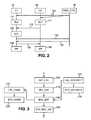
- FIG. 2there is shown therein the steps of a process, according to some embodiments, for switching the current mode of the first and the second cores of the CPU to a mode in which the first and the second cores cannot ensure the persistency of the sensible data in their entirely.
- the first core and the second coreare both in a full-feature mode
- the power management controllerhas received a command to switch the first and the second cores from a given mode of operation into a stand-by mode.
- the sensible data C1_S0 and C2_SDcannot be stored securely within the cores, and consequently cannot be restored when both cores return from stand-by mode to a full featured mode.
- the sensible data C1_S0 and C2-SDare generally too large to be kept entirely within the first and second persistent secure memory 55.
- the data of the secure environmentwhich have to be saved and restored, might have several origins.
- Said dataincludes the sensible data C1_S0 and C2_SD, which may comprise the contexts of the first and second cores. These data are dependent on the state of each core, meaning they have to be saved once per core. For example, referring to ARM cores, these data might be overall system control and configuration information, found in a system control coprocessor called "CP15". These data can also contain the contexts of lPs (not illustrated in Figure 1 ) linked to the cores via for example an interrupt controller.
- the CPUmay also comprise sensible data CPU_PSD related to the global CPU context, which have also to be saved and restored. These data, saved once globally, may be related to specific registers of lPs (not illustrated in Figure 1 ) linked to the CPU, and in a particular example to an interrupt controller or a snoop control unit.
- the data to be stored and restoredmay comprise the contents of one or more secure random access memories (not illustrated in Figure 1 ) included in the first and/or second cores and/or the CPU.
- Said memoriesmay comprise the content of stacks and/or heaps, instructions, static data related to the secure environment. In at least some embodiments, these data have to be saved once.
- the sensible data IP2_S0are specific to the contents of the second secure IP.
- the first and the second coresare in a first mode.
- One core amongst the first core and the second coreis identified as a master core, the other core being identified as a slave core.
- the master coreis the first core 50
- the slave coreis the second core 60.
- a step 100having received a request to switch the first and the second cores, to a second mode, the power management controller sends a first synchronization message to the master core and the slave core.
- the first synchronization messagecomprises information indicating the master and the slave cores that they must prepare themselves to enter into the second mode.
- the request to switch to the second modeis a secure interrupt. This embodiment allows direct communication between components involved in the switch without any additional link to an Operating System code.
- the master corestores the sensible data C1_SD in the shared persistent secure memory device 55. Before storing the sensible data C1_SD, unnecessary data present in the persistent secure memory device 55 may be cleared in order to free memory spaces. Alternatively, in an embodiment, the sensible data C1_SD may be stored in the public memory 40 in an encrypted form.
- the slave corestores the sensible data C2_SD in the shared persistent secure memory device 55. Before storing the sensible data C2_SD, unnecessary data present in the persistent secure memory device 55 may be cleared in order to free memory spaces. Alternatively, in an embodiment, the sensible data C2_SD may be stored in the public memory 40, in an encrypted form.
- the step 110 and the step 112may be performed sequentially, or in parallel.
- a step 115the slave core sends a second synchronization message to the master core, once the step 112 has been completed.
- the second synchronization messageis used to inform the master core that the context of the slave core has been saved.
- the master corestores, in the public memory 40, and in an encrypted form (thus, securely), sensible data other than sensible data C1_SD and C2_SD.
- This other sensible datamay be data handled by the processing device, which may include data related to the global CPU context, for example the sensible data CPU_SD. It may also be sensible data not bound to the processing device itself, such as an IP context or a memories context, for instance the sensible data IP2 _SD related to the second secure IP.
- a step 130the master core sends a third synchronization message to the power management controller, once the step 120 has been completed.
- the second synchronization messageis used to communicate result of the global context save operation performed during step 120 to the power management controller. For example, if an error has been detected or if all the operations have been performed as expected, the third synchronization message may contain information related to these events.
- a step 140the power management controller sends a fourth synchronization message to the master core to acknowledge the reception of the third synchronization message and and to communicate any error detected by the power management controller.
- this fourth messagenot only is used to acknowledge reception of the third message, but also to pass information about what happened on the power management controller side which could jeopardize entry into the stand-by mode (interrupts, errors, or other events).
- all possible errors thrown by the first core, the second core and the power management controller during the steps 130, 140 and 150may be intercepted and handled so as to exit properly of the low power mode entry sequence, and to give execution back to public code which has required the entry to the low power mode.
- a step 150having received the fourth synchronization message, the master core sends a fifth synchronization message to the slave core.
- the fifth synchronization messageis used to inform the slave core of any error previously detected or, alternatively, the success of all the operations previously performed by the master core and the power management controller.
- a step 160if no critical error has been reported in synchronization messages, the master core and the slave core switch to the second mode.
- the synchronization messagesmay be Fast Interrupt requests (FIQ).
- FIQFast Interrupt requests
- the synchronization messagescan be implemented using synchronous or asynchronous electric signals, interruptions, software notifications, or any other suitable software or hardware messaging means.
- FIG. 3there is shown therein the steps of a process, according to an embodiment, to store the sensible data, in the public memory 40, in an encrypted form, while switching to the second mode.
- This processcan be notably used to implement the step 110, 112 and/or 120.
- This processis to ensure that sensible data can't be corrupted, or retrieved when placed in public memory, e.g. when the first and the second cores are in a low power mode.
- a first step 200the sensible data to be stored are collected.
- sensible data that are not identified as mandatory to storeare not collected.
- specific core mode stacks and specific routines to define these stacks areacan be excluded from the mandatory data to store.
- only sensible data that are not already stored following a previous execution of this process and/or that have changed in the meantime,are identified as mandatory to store.
- the collected sensible dataare split into subsets.
- the size of each subsetmay be chosen equal to the size of the entries of the MMU, typically 4 Kbytes, to avoid processing related to the mapping of data as logical addresses inside MMU tables.
- all possible logical addressesare parsed, but real saving operations are based on physical addresses to fill a fixed length array in secure memory. Real size for the secure memory to be encrypted is then decreased significantly;
- a step 240the collected sensible data or the corresponding subsets are encrypted.
- an encryption schemeis used, for example, a symmetrical encryption scheme. Encryption allows avoiding public accesses to sensible data stored in the public memory.
- a step 225a first set of data is retrieved or generated.
- This set of datamay be cryptographic data.
- the cryptographic datamay be for example secret keys and/or cryptographic initialization vectors, used by the encryption scheme. More generally, cryptographic data are data which are the root of trust of the cryptographic mechanisms, like reference data used for all checks done on encrypted data.
- the cryptographic dataare stored in a persistent secure memory, said persistent secure memory being persistent at least when the cores are in the second mode.
- the persistent secure memorymay be the first and/or the second persistent secure memory 55.
- the encryption schememay use a different secret key for each subset. For example, a new secret key may be used every 4 Kbytes of encrypted sensible data. Consequently, two subsets of encrypted sensible data having an identical content are encrypted differently if they are not located on the same page, or at two different times on the same page.
- Each secret keycan be stored in the step 230. Alternatively, only a seed value used to generate with a crypto-algorithm every secret key may be stored, ensuring a high level of security and a low impact in terms of memory use.
- At least one hash valuemay be calculated, in a step 215, in applying a cryptographic hash function to the encrypted sensible data or to each encrypted subset.
- the calculated hash valueis stored in a persistent secure memory, said persistent secure memory being persistent at least when the cores are in the second mode.
- the persistent secure memorymay be the first and/or the second persistent secure memory 55, 65.
- the hash valuemay be used to check if a modification has been introduced in the encrypted sensible data.
- the encrypted sensible datais stored in a storage, for example the public storage 40, which is persistent at least when the cores are in the second mode.
- first step 200only sensible data that are not already stored in the external storage following a preceding execution of the process are collected.
- a comparison of the sensible data to collect with the encrypted sensible data already stored in the external storagecan be done using a hash function.
- the hash value calculated during step 215can be used for this purpose.
- FIG. 4there is shown therein the steps of a process, according to an embodiment, to restore the sensible data, following a switch from the second mode to another mode.
- This processcan be used to restore encrypted sensible data, stored in the external storage by the storing process described previously and on figure 3
- a step 300the encrypted sensible data or the subset stored in the external storage are retrieved.
- step 320the hash values stored in the persistent secure memory are retrieved.
- a step 330the cryptographic data stored in the persistent secure memory are retrieved.
- a step 310the retrieved encrypted sensible data or the corresponding subsets are decrypted using the retrieved cryptographic data and the cryptographic scheme.
- the cryptographic hash functionis applied to the retrieved encrypted sensible data or to each encrypted subset, and the hash values are compared to the hash values retrieved in the step 320. If the comparison fails, the retrieved encrypted sensible data are identified as modified.
- step 340if the decrypted sensible data comprise subsets, they are merged to reconstitute the sensible data.
- a step 350the decrypted sensible data are restored.
- the process to store or restore the sensible data as described aboveis inasmuch efficient that it can be integrated easily in the power strategy at system level. There may be a corresponding constraint on the proposed solution to maintain latency to a minimum value during the save/restore operation. If latency is not kept low enough, the gain of going into low power mode could be null or lost regarding the time required to enter this mode.
- the present inventioncan also be embedded in a computer program product, which comprises all the features enabling the implementation of the methods described herein, and which - when loaded in an information processing system - is able to carry out these methods.
- Computer program means or computer program in the present contextmean any expression, in any language, code or notation, of a set of instructions intended to cause a system having an information processing capability to perform a particular function either directly or after conversion to another language.
- Such a computer programcan be stored on a computer or machine readable medium allowing data, instructions, messages or message packets, and other machine readable information to be read from the medium.
- the computer or machine readable mediummay include non-volatile memory, such as ROM, Flash memory, Disk drive memory, CD-ROM, and other permanent storage. Additionally, a computer or machine readable medium may include, for example, volatile storage such as RAM, buffers, cache memory, and network circuits. Furthermore, the computer or machine readable medium may comprise computer or machine readable information in a transitory state medium such as a network link and/or a network interface, including a wired network or a wireless network, that allow a device to read such computer or machine readable information.
- a transitory state mediumsuch as a network link and/or a network interface, including a wired network or a wireless network, that allow a device to read such computer or machine readable information.
Landscapes
- Engineering & Computer Science (AREA)
- Theoretical Computer Science (AREA)
- Physics & Mathematics (AREA)
- Computer Hardware Design (AREA)
- General Engineering & Computer Science (AREA)
- General Physics & Mathematics (AREA)
- Computer Security & Cryptography (AREA)
- Software Systems (AREA)
- Mathematical Physics (AREA)
- Computing Systems (AREA)
- Storage Device Security (AREA)
Description
- The present invention generally relates to devices and methods for the management of a secure environment of a chip. It concerns more particularly the storage and/or the retrieving of sensitive data, in multicore systems, during transitional phases between an active mode and a low power mode of operation.
- The approaches described in this section could be pursued, but are not necessarily approaches that have been previously conceived or pursued. Therefore, unless otherwise indicated herein, the approaches described in this section are not prior art to the claims in this application and are not admitted to be prior art by inclusion in this section. Furthermore, all embodiments are not necessarily intended to solve all or even any of the problems brought forward in this section.
- A System-on-Chip (SoC) platform typically comprises at least one embedded Central Processing Unit (CPU), at least one embedded functional unit (also called an IP in the jargon of the one with ordinary skills in the art) which may be a memory (for instance of the eSRAM type), a Memory Management Unit (MMU), and/or at least one register. The components of the SoC are typically interconnected through an internal bus matrix.
- In operation, the SoC platform may be led to manipulate sensitive data, for instance, cryptographic secret keys or unencoded secret data like passwords. To prevent unauthorized access to and/or corruption of these sensitive data, the architecture of the SoC platform may be split into two physically and functionally separated environments: a secure environment for manipulating sensitive data and a public environment for processing non-sensitive data. The secure environment comprises notably one or more dedicated secure memories and/or one or more secure hardware registers to store sensitive data, whereas the public environment may include its own dedicated memories and/or hardware registers to store public data.
- This separation is for example implemented by Advanced RISC Machine (ARM) SoC platforms with security extensions, for example the TrustZone technology. A clear frontier between these two environments may be implemented with hardware (HW) and/or software (SW) mechanisms embedded in the processor, in the bus matrix, and in the IPs themselves. This frontier ensures that secure data within the secure environment cannot be accessed by any public component belonging to the public environment. This may typically be the case for normal modes of operation of the platform, wherein memories, IPs and processors are kept powered-on or in retention. However, some power modes are available wherein one or more of the secure components can be powered off, meaning that at least some of their contents have to be saved during the particular mode and be restored thereafter. Such modes may be available for the purpose of optimizing the power strategy of the chip and decrease energy leakages.
- US patent publication
US 6,209,088 B1 discloses a multi-core computer wherein a controlling process run by a boot-processor coordinates securely storing sensitive data of application processors before hibernation of the device. - A dedicated persistent secure memory, included in the secure environment, may be used to store securely sensitive data present in the secure environment before switching from a power-on mode to an energy saving mode. However, there might be cases where not enough secure memory space is available to save all secure contents. Consequently, in such cases, it may be necessary to store sensitive data outside the secure environment, in a non secure storage for example. It may be desirable that such storage can be made efficiency and securely.
- This task is rendered particularly difficult when the SoC platform comprises a CPU having a plurality of cores embedding security extensions, since the sensitive data may be spread between several cores.
- Another important issue may be to be able to guarantee data confidentiality and integrity to avoid leakage of secure information in the public environment during periods where secure data are stored in unsecure storage, and to avoid secure data corruption.
- Another aspect that may be considered concerns performances since one or several constraints may be inherent for low-power modes. The impact of the constraints on performances may preferably be as low as possible, so that the global platform strategy is not jeopardized.
- Thus, embodiments of the present invention aim at solving at least some of the following problems:
- How to store sensitive data handled by a multicore system in a first mode of operation, following a request to switch to a second mode of operation.
- Ensuring confidentiality and/or integrity for said stored sensitive data.
- Limiting impact on system performances.
- To address these needs, a first aspect of the present invention relates to a method of managing switching from a first mode of operation to a second mode, of a first core and at least one second core both included in a processor of a processing device. The processing device and the first and second cores of the processor are adapted to securely handle sensitive data when being in the first mode. The processing device further comprises a controller to control the switching to the second mode. The processor is coupled to a storage unit adapted to ensure persistency of data therein during periods of time when the first and the second cores are in the second mode. The method comprises the following steps:
- a step of sending, by the controller to the first core and to the second core, of a first message;
- upon reception of the first message by the first and second core respectively,
- ∘ a first step of storing securely sensitive data handled by the first core;
- ∘ a second step of storing securely sensitive data handled by the second core;
- a step of sending, by the second core to the first core, of a second message indicating the completion of the second step of storing;
- upon reception of the second message by the first core, a third step, driven by the first core, of storing securely, in the storage unit, other sensible data;
- a step of sending, by the first core to the controller of a third message indicating the completion of the third step of storing ;
- upon reception of the third message by the controller, a step of sending, by the controller to the first core, of a fourth message to acknowledge reception of the third message;
- upon reception of the fourth message by the first core, a step of sending, by the first core to the second core, of a fifth message;
- upon reception of the fourth and the fifth messages by the first and second cores respectively, a step of entering by the first and the second cores into the second mode.
- The third step of storing (driven by the first core) may comprise storing of sensible data handled by the processing device, such as, for example, a context common to the first and second cores (i.e. processor data). However, it should be noted that (alternatively or additionally) it may comprise storing of sensible data not bound to the processing device itself, such as an IP context or a memories context.
- The method according to some embodiments of the first aspect may allow reducing the power consumption of multicore processors by providing an efficient way to switch off the cores, without compromising the confidentiality of sensible data of the secure environment. The method according to some embodiments may provide a reliable and efficient solution to synchronize the switching of the different cores of the processor. Moreover, the amount of data that may be stored when the cores are in the second mode is in typical embodiments only limited by the available free space of the storage unit. Thus, in some embodiments, there is no need for the storage unit to provide security mechanisms for the purpose of protecting the secure data. Hence, the global cost and performance overhead of the method may be reduced.
- In some embodiments, at least one of the first, second and third steps of storing are performed by:
- collecting the sensitive data to be stored;
- encrypting, based on at least one first set of data, the collected sensitive data;
- storing the first set of data in a secure memory included in the processor, said secure memory being persistent during the periods of time when the first and the second cores are in the second mode;
- storing, in the storage unit, the encrypted sensitive data.
- According to some embodiments, the method can also further comprise a step, preceding the step of encrypting, wherein the collected sensitive data are split into subsets of sensitive data. Then, during the step of encrypting, a respective first set of data can be used for each subset of sensitive data, improving notably the confidentiality level of the method. In some embodiments, only a seed value used to generate the respective first set of data with a crypto-algorithm may be stored in the secure memory. Hence, the size of data stored in the secure memory is decreased.
- According to some embodiments, the method can also further comprise, to improve the integrity of the sensitive data, a step of generating a hash value, by applying a cryptographic hash function to the encrypted sensitive data or to each encrypted subset, and a step of storing the calculated hash value in the secure memory.
- According to some embodiments, the method can further comprise the following steps, when switching back from the second mode to the first mode of operation:
- retrieving the encrypted sensitive data or the subsets stored in the storage unit;
- retrieving the first set of data stored in the secure memory ;
- decrypting the retrieved encrypted sensitive data or the subsets using the retrieved first set of data;
- restoring the decrypted sensitive data.
- According to some embodiments, the method can further comprise the steps of :
- retrieving the hash values stored in the secure memory,
- calculating a hash value for the retrieved encrypted sensitive data or for each encrypted subsets, and
- comparing to the hash values retrieved from the secure memory to the calculated hash value;
- if the calculated hash value and the hash value stored in the secure memory mismatch, declaring corrupted or changed the corresponding retrieved encrypted sensitive data or the corresponding encrypted subset.
- A second aspect relates to a processing device including:
- ∘ a processor with a first core and at least one second core;
- ∘ a controller to manage switching from a first mode of operation to a second mode.
- The processing device and the first and second cores are adapted to securely handle sensitive data when being in the first mode. The processor is connectable to a storage unit adapted to ensure persistency of data therein during periods of time when the first and the second cores are in the second mode. The controller is configured to:
- send, to the first core and to the second core, a first message;
- upon reception of a third message; sending, to the first core, of a fourth message to acknowledge reception of a third message.
- The first core is configured to:
- upon reception of the first message, store securely sensitive data handled by the first core;
- upon reception of a second message, store securely, in the storage unit, other sensitive data;
- send, to the controller, the third message, indicating the completion of the storing of the other sensitive data;
- upon reception of the fourth message; send, a fifth message to the second core;
- upon reception of the fourth messages and having sent the fifth message, enter into the second mode.
- The second core is configured to:
- upon reception of the first message, store securely sensible data handled by the second core;
- send to the first core, the second message indicating the completion of the storing of the sensible data handled by the second core;
- upon reception of the fifth message, enter into the second mode.
- According to some embodiments, the first core and/or the second core are configured to store securely the sensible data by:
- collecting the sensible data to be stored;
- encrypting, based on at least one first set of data, the collected sensible data;
- storing the first set of data in a secure memory included in the processor, said secure memory being persistent during the periods of time when the first and the second cores are in the second mode;
- storing, in the storage unit, the encrypted sensible data.
- A third aspect relates to a processing system including a processor according to the second aspect and a storage unit adapted to ensure persistency of data therein during periods of time when the first and the second cores are in the second mode.
- A fourth aspect relates to an electronic device comprising a processing system according to the third aspect.
- A fifth aspect relates to a computer program product comprising one or more stored sequences of instructions that are accessible to a processor and which, when executed by the processor, cause the processor to carry out the steps of method according to the first aspect defined above.
- The present invention is illustrated by way of example, and not by way of limitation, in the figures of the accompanying drawings, in which like reference numerals refer to similar elements and in which:
Figure 1 is a schema of a processing device;Figure 2 is a flow chart illustrating steps of a process for switching the current mode of the first and the second cores of the CPU to a mode in which the first and the second cores cannot ensure the persistency of the sensible data in their entirety;Figure 3 is a flow chart illustrating steps of a process to store the sensible data in an encrypted form;Figure 4 is a flow chart illustrating steps of a process to restore the encrypted sensible data stored in a storage.- Expressions such as "comprise", "include", "incorporate", "contain", "is" and "have" are to be construed in a non-exclusive manner when interpreting the description and its associated claims, namely construed to allow for other items or components which are not explicitly defined also to be present. Reference to the singular is also to be construed in be a reference to the plural and vice versa.
- Referring now to
figure 1 , there is shown therein aprocessing device 10, according to an embodiment. The processing device comprises a processor orCPU 20, afirst IP 70, a secondsecure IP 75, aMMU 30, and apublic memory PD 40. TheMMU 30 manages the access of theCPU 20 to thepublic memory 40. The MMU is typically integrated to theCPU 20, and may be adapted to handle the accesses to the first IP, to the second secure IP, and to the public memory. In this embodiment and in the description above, the architecture of theprocessing device 10 is based on separate units respectively for theCPU 20, thefirst IP 70, the secondsecure IP 75, theMMU 30, and thepublic memory 40. However, it will be understood by those skilled in the art that various other architectures may be appropriate. In particular, the components of the processing device could be grouped, for example, on one chip. By way of an example, the processing device may be a SoC platform. - The processing device may be embedded in a mobile phone, a personal assistant, or an embedded device. The processing device may also be a part of a mobile or a desktop computer. The processing device may be adapted notably to run an operating system and/or platform specific softwares.
- The CPU comprises a
first core 50 and asecond core 60. Each core can be considered as a processor comprising notably its own arithmetic logic means to process instructions. In the embodiment illustrated byFigure 1 , the CPU comprises two cores. However, it will be understood that the CPU may comprise a greater number of cores, for example three, four, or more cores. - The
first core 50 is arranged to provide twovirtual processors virtual processor 52 is intended to be used to process non-sensitive data C1_PD in a context named public environment, whereas the secondvirtual processor 54 is dedicated to the processing of sensitive data C1_SD in a context named secure environment. - The
second core 60 is arranged to provide twovirtual processors virtual processor 62 is intended to be used to process non-sensitive data C2_PD in the public environment, whereas the secondvirtual processor 64 is dedicated to the processing of sensitive data C2_SD in the secure environment. - Notably the CPU is intended to be used to process sensitive data CPU_SD 56. The
sensitive data CPU_SD 56 handled by the CPU may be data related to software and hardware context in common for the CPU and the cores. - The CPU comprises a shared persistent
secure memory device 55 to securely store sensitive data of the secure environment, even during periods when the first and/or second core are in a low power or stand-by mode. Thefirst core 50 and/or thesecond core 60 may comprise also or alternatively persistent secure memories (not illustrated inFigure 1 ) to store sensitive data of the secure environment, even during periods when the first and/or second core are in a low power or stand-by mode. - The
first IP 70 is only intended to manage non-sensible data IP1_PD in the public environment. The secondsecure IP 75 is intended to handle sensible data lP2_SD in the secure environment. - The
public memory 40 is persistent during periods when the first core and/or the second core are in a low power or stand-by mode. Stated otherwise, the storage and the persistency of the data stored in the public memory are independent of the operational mode of the cores. - The
processing device 10 comprises also apower management controller 80, coupled to theCPU 20. Thepower management controller 80 handles the transitions between a plurality of operational modes of theprocessing device 10. An operational mode defines a state in which a core provides a given set of functionalities at a given level of performances. For example, a full-feature mode may correspond to a state in which a core provides all its functionalities at its highest level of performances. A low power mode may correspond to a state in which a core provides only a subset of its functionalities at a lowered level of performances, some unused parts of the core being possibly powered-off. A stand-by mode may correspond to a state in which a core provides only a wake-up on events functionality, several parts of the core being powered-off. Depending on the design of the first core and the second core, thepower management controller 80 may manage transitions between the different modes of the first and second core independently, or co-jointly. Thepower management controller 80 may also be configured to handle the transitions between two or more operational modes of thefirst IP 70 and/or the secondsecure IP 75. In a basic setup, the power management controller may be configured to handle the transition between a first mode and a second mode, the second mode being a stand-by mode, a low-power power mode, a power off mode, or a restricted functionality mode, for example. - In one embodiment, the
CPU 20 is an ARM CPU, with security extensions, for example the TrustZone technology. - Referring now to
Figure 2 , there is shown therein the steps of a process, according to some embodiments, for switching the current mode of the first and the second cores of the CPU to a mode in which the first and the second cores cannot ensure the persistency of the sensible data in their entirely. For example, the first core and the second core are both in a full-feature mode, and the power management controller has received a command to switch the first and the second cores from a given mode of operation into a stand-by mode. When both cores are in stand-by mode, the sensible data C1_S0 and C2_SD cannot be stored securely within the cores, and consequently cannot be restored when both cores return from stand-by mode to a full featured mode. In particular, the sensible data C1_S0 and C2-SD are generally too large to be kept entirely within the first and second persistentsecure memory 55. - The data of the secure environment, which have to be saved and restored, might have several origins.
- Said data includes the sensible data C1_S0 and C2_SD, which may comprise the contexts of the first and second cores. These data are dependent on the state of each core, meaning they have to be saved once per core. For example, referring to ARM cores, these data might be overall system control and configuration information, found in a system control coprocessor called "CP15". These data can also contain the contexts of lPs (not illustrated in
Figure 1 ) linked to the cores via for example an interrupt controller. - The CPU may also comprise sensible data CPU_PSD related to the global CPU context, which have also to be saved and restored. These data, saved once globally, may be related to specific registers of lPs (not illustrated in
Figure 1 ) linked to the CPU, and in a particular example to an interrupt controller or a snoop control unit. - The data to be stored and restored may comprise the contents of one or more secure random access memories (not illustrated in
Figure 1 ) included in the first and/or second cores and/or the CPU. Said memories may comprise the content of stacks and/or heaps, instructions, static data related to the secure environment. In at least some embodiments, these data have to be saved once. The sensible data IP2_S0 are specific to the contents of the second secure IP. - Initially, the first and the second cores are in a first mode. One core amongst the first core and the second core is identified as a master core, the other core being identified as a slave core. In
Figure 2 , the master core is thefirst core 50, whereas the slave core is thesecond core 60. - In a
step 100, having received a request to switch the first and the second cores, to a second mode, the power management controller sends a first synchronization message to the master core and the slave core. The first synchronization message comprises information indicating the master and the slave cores that they must prepare themselves to enter into the second mode. In one embodiment of thestep 100, the request to switch to the second mode is a secure interrupt. This embodiment allows direct communication between components involved in the switch without any additional link to an Operating System code. - In a
step 110, the master core stores the sensible data C1_SD in the shared persistentsecure memory device 55. Before storing the sensible data C1_SD, unnecessary data present in the persistentsecure memory device 55 may be cleared in order to free memory spaces. Alternatively, in an embodiment, the sensible data C1_SD may be stored in thepublic memory 40 in an encrypted form. - In a
step 112, the slave core stores the sensible data C2_SD in the shared persistentsecure memory device 55. Before storing the sensible data C2_SD, unnecessary data present in the persistentsecure memory device 55 may be cleared in order to free memory spaces. Alternatively, in an embodiment, the sensible data C2_SD may be stored in thepublic memory 40, in an encrypted form. - The
step 110 and thestep 112 may be performed sequentially, or in parallel. - In a
step 115, the slave core sends a second synchronization message to the master core, once thestep 112 has been completed. - The second synchronization message is used to inform the master core that the context of the slave core has been saved.
- In a
step 120, the master core stores, in thepublic memory 40, and in an encrypted form (thus, securely), sensible data other than sensible data C1_SD and C2_SD. This other sensible data may be data handled by the processing device, which may include data related to the global CPU context, for example the sensible data CPU_SD. It may also be sensible data not bound to the processing device itself, such as an IP context or a memories context, for instance the sensible data IP2 _SD related to the second secure IP. - In a
step 130, the master core sends a third synchronization message to the power management controller, once thestep 120 has been completed. The second synchronization message is used to communicate result of the global context save operation performed duringstep 120 to the power management controller. For example, if an error has been detected or if all the operations have been performed as expected, the third synchronization message may contain information related to these events. - In a
step 140, the power management controller sends a fourth synchronization message to the master core to acknowledge the reception of the third synchronization message and and to communicate any error detected by the power management controller. Stated otherwise, this fourth message not only is used to acknowledge reception of the third message, but also to pass information about what happened on the power management controller side which could jeopardize entry into the stand-by mode (interrupts, errors, or other events...). In fact, all possible errors thrown by the first core, the second core and the power management controller during thesteps - In a
step 150, having received the fourth synchronization message, the master core sends a fifth synchronization message to the slave core. The fifth synchronization message is used to inform the slave core of any error previously detected or, alternatively, the success of all the operations previously performed by the master core and the power management controller. - In a
step 160, if no critical error has been reported in synchronization messages, the master core and the slave core switch to the second mode. - In one embodiment, related to ARM cores, the synchronization messages may be Fast Interrupt requests (FIQ). Alternatively, the synchronization messages can be implemented using synchronous or asynchronous electric signals, interruptions, software notifications, or any other suitable software or hardware messaging means.
- Referring now to
Figure 3 , there is shown therein the steps of a process, according to an embodiment, to store the sensible data, in thepublic memory 40, in an encrypted form, while switching to the second mode. This process can be notably used to implement thestep - This process is to ensure that sensible data can't be corrupted, or retrieved when placed in public memory, e.g. when the first and the second cores are in a low power mode.
- In a
first step 200, the sensible data to be stored are collected. - In an embodiment of the
first step 200, sensible data that are not identified as mandatory to store are not collected. For example, specific core mode stacks and specific routines to define these stacks area can be excluded from the mandatory data to store. In an embodiment, only sensible data that are not already stored following a previous execution of this process and/or that have changed in the meantime, are identified as mandatory to store. - In an
optional step 210, the collected sensible data are split into subsets. The size of each subset may be chosen equal to the size of the entries of the MMU, typically 4 Kbytes, to avoid processing related to the mapping of data as logical addresses inside MMU tables. In some embodiments, all possible logical addresses are parsed, but real saving operations are based on physical addresses to fill a fixed length array in secure memory. Real size for the secure memory to be encrypted is then decreased significantly; - In a
step 240, the collected sensible data or the corresponding subsets are encrypted. In an embodiment of thestep 240, an encryption scheme is used, for example, a symmetrical encryption scheme. Encryption allows avoiding public accesses to sensible data stored in the public memory. To apply the encryption scheme, in astep 225, a first set of data is retrieved or generated. This set of data may be cryptographic data. The cryptographic data may be for example secret keys and/or cryptographic initialization vectors, used by the encryption scheme. More generally, cryptographic data are data which are the root of trust of the cryptographic mechanisms, like reference data used for all checks done on encrypted data. In astep 230, the cryptographic data are stored in a persistent secure memory, said persistent secure memory being persistent at least when the cores are in the second mode. For example, the persistent secure memory may be the first and/or the second persistentsecure memory 55. - To increase the security level, the encryption scheme may use a different secret key for each subset. For example, a new secret key may be used every 4 Kbytes of encrypted sensible data. Consequently, two subsets of encrypted sensible data having an identical content are encrypted differently if they are not located on the same page, or at two different times on the same page. Each secret key can be stored in the
step 230. Alternatively, only a seed value used to generate with a crypto-algorithm every secret key may be stored, ensuring a high level of security and a low impact in terms of memory use. - At least one hash value may be calculated, in a
step 215, in applying a cryptographic hash function to the encrypted sensible data or to each encrypted subset. In astep 220, the calculated hash value is stored in a persistent secure memory, said persistent secure memory being persistent at least when the cores are in the second mode. For example, the persistent secure memory may be the first and/or the second persistentsecure memory 55, 65. The hash value may be used to check if a modification has been introduced in the encrypted sensible data. - In a
step 250, the encrypted sensible data is stored in a storage, for example thepublic storage 40, which is persistent at least when the cores are in the second mode. - In an embodiment of the
first step 200, only sensible data that are not already stored in the external storage following a preceding execution of the process are collected. For example, a comparison of the sensible data to collect with the encrypted sensible data already stored in the external storage can be done using a hash function. The hash value calculated duringstep 215 can be used for this purpose. Alternatively, it is possible to detect any changes of the sensible data, or of the subsets, since the preceding execution of the process, for example by flagging all synchronous or asynchronous entries inside the secure environment. If the sensible data or the subsets have not been modified and if they are already stored on the external storage, they are not collected. - Referring now to
Figure 4 , there is shown therein the steps of a process, according to an embodiment, to restore the sensible data, following a switch from the second mode to another mode. This process can be used to restore encrypted sensible data, stored in the external storage by the storing process described previously and onfigure 3 - In a
step 300, the encrypted sensible data or the subset stored in the external storage are retrieved. - In an
optional step 320, the hash values stored in the persistent secure memory are retrieved. - In a
step 330, the cryptographic data stored in the persistent secure memory are retrieved. - In a
step 310, the retrieved encrypted sensible data or the corresponding subsets are decrypted using the retrieved cryptographic data and the cryptographic scheme. Optionally, during thestep 310, the cryptographic hash function is applied to the retrieved encrypted sensible data or to each encrypted subset, and the hash values are compared to the hash values retrieved in thestep 320. If the comparison fails, the retrieved encrypted sensible data are identified as modified. - In an
optional step 340, if the decrypted sensible data comprise subsets, they are merged to reconstitute the sensible data. - In a
step 350, the decrypted sensible data are restored. - The process to store or restore the sensible data as described above is inasmuch efficient that it can be integrated easily in the power strategy at system level. There may be a corresponding constraint on the proposed solution to maintain latency to a minimum value during the save/restore operation. If latency is not kept low enough, the gain of going into low power mode could be null or lost regarding the time required to enter this mode.
- Several embodiments of the store and/or restore process proposed are aimed at addressing these performances aspects, and can be adopted either alone or in combination. The present invention can also be embedded in a computer program product, which comprises all the features enabling the implementation of the methods described herein, and which - when loaded in an information processing system - is able to carry out these methods. Computer program means or computer program in the present context mean any expression, in any language, code or notation, of a set of instructions intended to cause a system having an information processing capability to perform a particular function either directly or after conversion to another language. Such a computer program can be stored on a computer or machine readable medium allowing data, instructions, messages or message packets, and other machine readable information to be read from the medium. The computer or machine readable medium may include non-volatile memory, such as ROM, Flash memory, Disk drive memory, CD-ROM, and other permanent storage. Additionally, a computer or machine readable medium may include, for example, volatile storage such as RAM, buffers, cache memory, and network circuits. Furthermore, the computer or machine readable medium may comprise computer or machine readable information in a transitory state medium such as a network link and/or a network interface, including a wired network or a wireless network, that allow a device to read such computer or machine readable information.
Claims (15)
- A method of managing switching from a first mode of operation to a second mode, of a first core (50) and at least one second core (60) both included in a processor (20) of a processing device (10), the processing device and the first and second cores being adapted to securely handle sensitive data when being in the first mode, the processing device further comprising a controller (80) to control the switching to the second mode, the processor being coupled to a storage unit (40) adapted to ensure persistency of data therein during periods of time when the first and the second cores are in the second mode, the method beingcharacterized in that it comprises the following steps:• a step of sending (100), by the controller to the first core and to the second core, of a first message;• upon reception of the first message by the first and second core respectively,∘ a first step of storing securely (110) sensitive data handled by the first core, and∘ a second step of storing securely (112) sensitive data handled by the second core;• a step of sending (115), by the second core to the first core, of a second message indicating the completion of the second step of storing;• upon reception of the second message by the first core, a third step, handled by the first core, of storing securely (120), in the storage unit, other sensitive data;• a step of sending (130), by the first core to the controller of a third message indicating the completion of the third step of storing ;• upon reception of the third message by the controller, a step of sending (140), by the controller to the first core, of a fourth message to acknowledge reception of the third message;• upon reception of the fourth message by the first core, a step of sending (150), by the first core to the second core, of a fifth message;• upon reception of the fourth and the fifth messages by the first and second cores respectively, a step of entering (160) by the first and the second cores into the second mode.
- The method of claim 1, wherein at least one of the first, second and third steps of storing (110, 112, 120) are performed by:• collecting (200) the sensitive data to be stored;• encrypting (240), based on at least one first set of data, the collected sensitive data;• storing (230) the first set of data in a secure memory (56) included in the processor, said secure memory being persistent during the periods of time when the first and the second cores are in the second mode;• storing (250), in the storage unit, the encrypted sensitive data.
- The method of claim 2, wherein during the step of collecting (200) of sensitive data, only sensitive data identified as being mandatory to store are collected.
- The method of claim 2 or 3, wherein during the step of collecting (200) of sensitive data, only sensitive data that are not already stored are collected.
- The method of any one of claims 2 to 4, further comprising a step (210), preceding the step of encrypting (240), wherein the collected sensitive data are split into subsets of sensitive data.
- The method of claim 5, wherein during the step of encrypting (240), a respective first set of data is used to encrypt each subset of sensitive data.
- The method of claim 6, wherein only a seed value used to generate the respective first set of data with a crypto-algorithm is stored (230) in the secure memory.
- The method of any one of claims 2 to 7, further comprising a step of generating (215) a hash value, by applying a cryptographic hash function to the encrypted sensitive data or to each encrypted subset, and a step (220) of storing the calculated hash value in the secure memory.
- The method of any one of claims 2 to 8, further comprising the following steps, when switching back from the second mode to the first mode of operation:• retrieving (300) the encrypted sensitive data or the subsets stored in the storage unit;• retrieving (330) the first set of data stored in the secure memory ;• decrypting (310) the retrieved encrypted sensitive data or the subsets using the retrieved first set of data;• restoring (350) the decrypted sensitive data.
- The method of claim 9 and claim 8, further comprising the steps of:• retrieving (320) the hash values stored in the secure memory,• calculating a hash value for the retrieved encrypted sensitive data or for each encrypted subsets, and• comparing to the hash values retrieved from the secure memory to the calculated hash value;• if the calculated hash value and the hash value retrieved from the secure memory mismatch, declaring corrupted or changed the corresponding retrieved encrypted sensitive data or the corresponding encrypted subset.
- A processing device (20) including:∘ a processor with a first core (50) and at least one second core (60);∘ a controller (80) to manage switching from a first mode of operation to a second mode ;
the processing unit and the first and second cores being adapted to securely handle sensitive data when being in the first mode, the processor being connectable to a storage unit (40) adapted to ensure persistency of data therein during periods of time when the first and the second cores are in the second mode,characterized in that the controller is configured to:• send (100), to the first core and to the second core, a first message;• upon reception of a third message; sending (140), to the first core, of a fourth message to acknowledge reception of a third message;the first core being configured to :• upon reception of the first message, store securely (110) sensitive data handled by the first core;• upon reception of a second message, store securely, in the storage unit, other sensitive data;• send (130), to the controller, the third message, indicating the completion of the storing of the sensitive data handled by the processing device ;• upon reception of the fourth message; send (150), a fifth message to the second core;• upon reception of the fourth messages and having sent the fifth message, enter (160) into the second mode;the second core being configured to:• upon reception of the first message, store securely (112) sensitive data handled by the second core;• send (115) to the first core, the second message indicating the completion of the storing (112) of the sensitive data handled by the second core;• upon reception of the fifth message, enter (160) into the second mode. - The processing device of claim 11, wherein the first core and/or the second core are configured to store securely the sensitive data by:• collecting (200) the sensitive data to be stored;• encrypting (240), based on at least one first set of data, the collected sensitive data;• storing (230) the first set of data in a secure memory (56) included in the processor, said secure memory being persistent during the periods of time when the first and the second cores are in the second mode;• storing (250), in the storage unit, the encrypted sensitive data.
- The processing device of any of claims 11 and 12, further including the storage unit (40) adapted to ensure persistency of data therein during periods of time when the first and the second cores are in the second mode.
- An electronic device comprising a processing device according to any of claims 11 to 13.
- A computer program product comprising a computer readable medium having stored thereon one or more sequences of instructions that are accessible to a processor and which, when executed by the processor, cause the processor to carry out the steps of any of Claims 1 to 10.
Priority Applications (5)
| Application Number | Priority Date | Filing Date | Title |
|---|---|---|---|
| EP10191115.4AEP2360611B1 (en) | 2010-01-22 | 2010-11-12 | Secure environment management during switches between different modes of multicore systems |
| KR1020127019276AKR20130020880A (en) | 2010-01-22 | 2011-01-21 | Secure environment management during switches between different modes of multicore systems |
| US13/574,548US8862898B2 (en) | 2010-01-22 | 2011-01-21 | Secure environment management during switches between different modes of multicore systems |
| PCT/EP2011/050848WO2011089231A1 (en) | 2010-01-22 | 2011-01-21 | Secure environment management during switches between different modes of multicore systems |
| CN201180015295.4ACN102844762B (en) | 2010-01-22 | 2011-01-21 | Secure environment management during switches between different modes of multicore systems |
Applications Claiming Priority (2)
| Application Number | Priority Date | Filing Date | Title |
|---|---|---|---|
| EP10305077 | 2010-01-22 | ||
| EP10191115.4AEP2360611B1 (en) | 2010-01-22 | 2010-11-12 | Secure environment management during switches between different modes of multicore systems |
Publications (2)
| Publication Number | Publication Date |
|---|---|
| EP2360611A1 EP2360611A1 (en) | 2011-08-24 |
| EP2360611B1true EP2360611B1 (en) | 2014-09-10 |
Family
ID=43638798
Family Applications (1)
| Application Number | Title | Priority Date | Filing Date |
|---|---|---|---|
| EP10191115.4ANot-in-forceEP2360611B1 (en) | 2010-01-22 | 2010-11-12 | Secure environment management during switches between different modes of multicore systems |
Country Status (5)
| Country | Link |
|---|---|
| US (1) | US8862898B2 (en) |
| EP (1) | EP2360611B1 (en) |
| KR (1) | KR20130020880A (en) |
| CN (1) | CN102844762B (en) |
| WO (1) | WO2011089231A1 (en) |
Families Citing this family (49)
| Publication number | Priority date | Publication date | Assignee | Title |
|---|---|---|---|---|
| EP2581850B1 (en)* | 2011-10-11 | 2018-12-12 | OCT Circuit Technologies International Limited | Increased flexibility of security framework during low power modes management |
| US9027102B2 (en) | 2012-05-11 | 2015-05-05 | Sprint Communications Company L.P. | Web server bypass of backend process on near field communications and secure element chips |
| US9282898B2 (en) | 2012-06-25 | 2016-03-15 | Sprint Communications Company L.P. | End-to-end trusted communications infrastructure |
| US9183412B2 (en) | 2012-08-10 | 2015-11-10 | Sprint Communications Company L.P. | Systems and methods for provisioning and using multiple trusted security zones on an electronic device |
| US9451394B2 (en) | 2012-12-31 | 2016-09-20 | Elwha Llc | Cost-effective mobile connectivity protocols |
| US9832628B2 (en) | 2012-12-31 | 2017-11-28 | Elwha, Llc | Cost-effective mobile connectivity protocols |
| US9876762B2 (en)* | 2012-12-31 | 2018-01-23 | Elwha Llc | Cost-effective mobile connectivity protocols |
| US9781664B2 (en) | 2012-12-31 | 2017-10-03 | Elwha Llc | Cost-effective mobile connectivity protocols |
| US8965288B2 (en) | 2012-12-31 | 2015-02-24 | Elwha Llc | Cost-effective mobile connectivity protocols |
| US9635605B2 (en) | 2013-03-15 | 2017-04-25 | Elwha Llc | Protocols for facilitating broader access in wireless communications |
| US9713013B2 (en) | 2013-03-15 | 2017-07-18 | Elwha Llc | Protocols for providing wireless communications connectivity maps |
| US9980114B2 (en) | 2013-03-15 | 2018-05-22 | Elwha Llc | Systems and methods for communication management |
| US9578664B1 (en) | 2013-02-07 | 2017-02-21 | Sprint Communications Company L.P. | Trusted signaling in 3GPP interfaces in a network function virtualization wireless communication system |
| US9613208B1 (en) | 2013-03-13 | 2017-04-04 | Sprint Communications Company L.P. | Trusted security zone enhanced with trusted hardware drivers |
| US9596584B2 (en) | 2013-03-15 | 2017-03-14 | Elwha Llc | Protocols for facilitating broader access in wireless communications by conditionally authorizing a charge to an account of a third party |
| US9693214B2 (en) | 2013-03-15 | 2017-06-27 | Elwha Llc | Protocols for facilitating broader access in wireless communications |
| US9781554B2 (en) | 2013-03-15 | 2017-10-03 | Elwha Llc | Protocols for facilitating third party authorization for a rooted communication device in wireless communications |
| US9374363B1 (en)* | 2013-03-15 | 2016-06-21 | Sprint Communications Company L.P. | Restricting access of a portable communication device to confidential data or applications via a remote network based on event triggers generated by the portable communication device |
| US9843917B2 (en) | 2013-03-15 | 2017-12-12 | Elwha, Llc | Protocols for facilitating charge-authorized connectivity in wireless communications |
| US9813887B2 (en) | 2013-03-15 | 2017-11-07 | Elwha Llc | Protocols for facilitating broader access in wireless communications responsive to charge authorization statuses |
| US9866706B2 (en) | 2013-03-15 | 2018-01-09 | Elwha Llc | Protocols for facilitating broader access in wireless communications |
| US9706382B2 (en) | 2013-03-15 | 2017-07-11 | Elwha Llc | Protocols for allocating communication services cost in wireless communications |
| US9706060B2 (en) | 2013-03-15 | 2017-07-11 | Elwha Llc | Protocols for facilitating broader access in wireless communications |
| US9807582B2 (en) | 2013-03-15 | 2017-10-31 | Elwha Llc | Protocols for facilitating broader access in wireless communications |
| US9324016B1 (en) | 2013-04-04 | 2016-04-26 | Sprint Communications Company L.P. | Digest of biographical information for an electronic device with static and dynamic portions |
| US9454723B1 (en) | 2013-04-04 | 2016-09-27 | Sprint Communications Company L.P. | Radio frequency identity (RFID) chip electrically and communicatively coupled to motherboard of mobile communication device |
| US9838869B1 (en) | 2013-04-10 | 2017-12-05 | Sprint Communications Company L.P. | Delivering digital content to a mobile device via a digital rights clearing house |
| US9443088B1 (en) | 2013-04-15 | 2016-09-13 | Sprint Communications Company L.P. | Protection for multimedia files pre-downloaded to a mobile device |
| US9560519B1 (en) | 2013-06-06 | 2017-01-31 | Sprint Communications Company L.P. | Mobile communication device profound identity brokering framework |
| TWI516982B (en)* | 2014-04-22 | 2016-01-11 | 晨星半導體股份有限公司 | Computing device and method of processing secure services for computing device |
| WO2015196449A1 (en) | 2014-06-27 | 2015-12-30 | Microsoft Technology Licensing, Llc | Data protection system based on user input patterns on device |
| WO2015196444A1 (en)* | 2014-06-27 | 2015-12-30 | Microsoft Technology Licensing, Llc | Fast data protection using dual file systems |
| WO2015196450A1 (en) | 2014-06-27 | 2015-12-30 | Microsoft Technology Licensing, Llc | System for data protection in power off mode |
| CN105519038B (en) | 2014-06-27 | 2020-03-17 | 微软技术许可有限责任公司 | User input data protection method and system |
| US9779232B1 (en) | 2015-01-14 | 2017-10-03 | Sprint Communications Company L.P. | Trusted code generation and verification to prevent fraud from maleficent external devices that capture data |
| US9838868B1 (en) | 2015-01-26 | 2017-12-05 | Sprint Communications Company L.P. | Mated universal serial bus (USB) wireless dongles configured with destination addresses |
| US9473945B1 (en) | 2015-04-07 | 2016-10-18 | Sprint Communications Company L.P. | Infrastructure for secure short message transmission |
| US10078356B2 (en)* | 2015-08-20 | 2018-09-18 | Intel Corporation | Apparatus and method for saving and restoring data for power saving in a processor |
| US9819679B1 (en) | 2015-09-14 | 2017-11-14 | Sprint Communications Company L.P. | Hardware assisted provenance proof of named data networking associated to device data, addresses, services, and servers |
| US10282719B1 (en) | 2015-11-12 | 2019-05-07 | Sprint Communications Company L.P. | Secure and trusted device-based billing and charging process using privilege for network proxy authentication and audit |
| US9817992B1 (en) | 2015-11-20 | 2017-11-14 | Sprint Communications Company Lp. | System and method for secure USIM wireless network access |
| CN106127059B (en)* | 2016-06-30 | 2019-03-29 | 中国船舶重工集团公司第七0九研究所 | The realization of credible password module and method of servicing on a kind of ARM platform |
| CN106407561B (en)* | 2016-09-19 | 2020-07-03 | 复旦大学 | A division method of parallel GPDT algorithm on multi-core SOC |
| US10503892B2 (en) | 2017-06-25 | 2019-12-10 | Microsoft Technology Licensing, Llc | Remote attestation for multi-core processor |
| US10708061B2 (en)* | 2017-06-25 | 2020-07-07 | Microsoft Technology Licensing, Llc | Secure key storage for multi-core processor |
| US10499249B1 (en) | 2017-07-11 | 2019-12-03 | Sprint Communications Company L.P. | Data link layer trust signaling in communication network |
| US20190101969A1 (en)* | 2017-09-29 | 2019-04-04 | Intel Corporation | Control Blocks for Processor Power Management |
| FR3076920B1 (en)* | 2018-01-16 | 2019-12-13 | Continental Automotive France | METHOD FOR REPROGRAMMING DATA OF A SOFTWARE FUNCTION EXECUTED BY AT LEAST ONE COMPUTER PROVIDED WITH AT LEAST ONE EXECUTION CORE, AT LEAST ONE SECURITY CORE AND AT LEAST ONE NON-VOLATILE MEMORY |
| JP7266067B2 (en)* | 2021-06-25 | 2023-04-27 | 株式会社日立製作所 | storage system |
Family Cites Families (7)
| Publication number | Priority date | Publication date | Assignee | Title |
|---|---|---|---|---|
| IL137855A0 (en)* | 1998-02-18 | 2001-10-31 | Voltaire Advanced Data Securit | Information security method and apparatus |
| US6209088B1 (en)* | 1998-09-21 | 2001-03-27 | Microsoft Corporation | Computer hibernation implemented by a computer operating system |
| GB2403561A (en)* | 2003-07-02 | 2005-01-05 | Advanced Risc Mach Ltd | Power control within a coherent multi-processor system |
| GB2446658B (en)* | 2007-02-19 | 2011-06-08 | Advanced Risc Mach Ltd | Hibernating a processing apparatus for processing secure data |
| US20080226078A1 (en)* | 2007-03-12 | 2008-09-18 | Microsoft Corporation | Enabling recording and copying data |
| US7730248B2 (en)* | 2007-12-13 | 2010-06-01 | Texas Instruments Incorporated | Interrupt morphing and configuration, circuits, systems and processes |
| US8775824B2 (en)* | 2008-01-02 | 2014-07-08 | Arm Limited | Protecting the security of secure data sent from a central processor for processing by a further processing device |
- 2010
- 2010-11-12EPEP10191115.4Apatent/EP2360611B1/ennot_activeNot-in-force
- 2011
- 2011-01-21USUS13/574,548patent/US8862898B2/ennot_activeExpired - Fee Related
- 2011-01-21KRKR1020127019276Apatent/KR20130020880A/ennot_activeAbandoned
- 2011-01-21WOPCT/EP2011/050848patent/WO2011089231A1/enactiveApplication Filing
- 2011-01-21CNCN201180015295.4Apatent/CN102844762B/ennot_activeExpired - Fee Related
Also Published As
| Publication number | Publication date |
|---|---|
| KR20130020880A (en) | 2013-03-04 |
| CN102844762B (en) | 2015-06-03 |
| CN102844762A (en) | 2012-12-26 |
| US20120297202A1 (en) | 2012-11-22 |
| EP2360611A1 (en) | 2011-08-24 |
| US8862898B2 (en) | 2014-10-14 |
| WO2011089231A1 (en) | 2011-07-28 |
Similar Documents
| Publication | Publication Date | Title |
|---|---|---|
| EP2360611B1 (en) | Secure environment management during switches between different modes of multicore systems | |
| US7392415B2 (en) | Sleep protection | |
| EP3706361B1 (en) | Loading and virtualizing cryptographic keys | |
| JP5784677B2 (en) | Extending the processor for secure embedded container execution | |
| KR102013841B1 (en) | Method of managing key for secure storage of data, and and apparatus there-of | |
| US20200110880A1 (en) | Systems, apparatuses, and methods for platform security | |
| JP5875601B2 (en) | System and method for in-place encryption | |
| US10216648B2 (en) | Maintaining a secure processing environment across power cycles | |
| CN112149146A (en) | Deterministic encryption key rotation | |
| US20030033537A1 (en) | Tamper resistant microprocessor using fast context switching | |
| US12197631B2 (en) | Security management of ferroelectric memory device | |
| Shafiee et al. | Secure DIMM: Moving ORAM primitives closer to memory | |
| US20100128874A1 (en) | Encryption / decryption in parallelized data storage using media associated keys | |
| US20150205732A1 (en) | Seamlessly encrypting memory regions to protect against hardware-based attacks | |
| JP2012508938A (en) | Secure application execution method and apparatus | |
| US20180097839A1 (en) | Systems, apparatuses, and methods for platform security | |
| WO2014098998A1 (en) | Securing data transmissions between processor packages | |
| Yuan et al. | Pssm: Achieving secure memory for gpus with partitioned and sectored security metadata | |
| Liu et al. | Ps-oram: Efficient crash consistency support for oblivious ram on nvm | |
| EP4202740A1 (en) | Process object re-keying during process creation in cryptographic computing | |
| Enck et al. | Defending against attacks on main memory persistence | |
| US20240007265A1 (en) | Data authenticity and integrity check for data security schemes | |
| CN111324910A (en) | Method for realizing memory database by TrustZone technology | |
| Chiavassa et al. | Secure Intermittent Computing with ARM TrustZone on the Cortex-M | |
| JP2004272816A (en) | Multitask execution system and multitask execution method |
Legal Events
| Date | Code | Title | Description |
|---|---|---|---|
| PUAI | Public reference made under article 153(3) epc to a published international application that has entered the european phase | Free format text:ORIGINAL CODE: 0009012 | |
| AK | Designated contracting states | Kind code of ref document:A1 Designated state(s):AL AT BE BG CH CY CZ DE DK EE ES FI FR GB GR HR HU IE IS IT LI LT LU LV MC MK MT NL NO PL PT RO RS SE SI SK SM TR | |
| AX | Request for extension of the european patent | Extension state:BA ME | |
| 17P | Request for examination filed | Effective date:20111118 | |
| 17Q | First examination report despatched | Effective date:20121217 | |
| REG | Reference to a national code | Ref country code:DE Ref legal event code:R079 Ref document number:602010018841 Country of ref document:DE Free format text:PREVIOUS MAIN CLASS: G06F0021000000 Ipc:G06F0001320000 | |
| RIC1 | Information provided on ipc code assigned before grant | Ipc:G06F 21/74 20130101ALI20140507BHEP Ipc:G06F 21/81 20130101ALI20140507BHEP Ipc:G06F 1/32 20060101AFI20140507BHEP | |
| GRAP | Despatch of communication of intention to grant a patent | Free format text:ORIGINAL CODE: EPIDOSNIGR1 | |
| INTG | Intention to grant announced | Effective date:20140613 | |
| GRAS | Grant fee paid | Free format text:ORIGINAL CODE: EPIDOSNIGR3 | |
| GRAA | (expected) grant | Free format text:ORIGINAL CODE: 0009210 | |
| AK | Designated contracting states | Kind code of ref document:B1 Designated state(s):AL AT BE BG CH CY CZ DE DK EE ES FI FR GB GR HR HU IE IS IT LI LT LU LV MC MK MT NL NO PL PT RO RS SE SI SK SM TR | |
| REG | Reference to a national code | Ref country code:GB Ref legal event code:FG4D | |
| REG | Reference to a national code | Ref country code:CH Ref legal event code:EP | |
| REG | Reference to a national code | Ref country code:IE Ref legal event code:FG4D | |
| REG | Reference to a national code | Ref country code:AT Ref legal event code:REF Ref document number:687000 Country of ref document:AT Kind code of ref document:T Effective date:20141015 | |
| REG | Reference to a national code | Ref country code:DE Ref legal event code:R096 Ref document number:602010018841 Country of ref document:DE Effective date:20141023 | |
| PG25 | Lapsed in a contracting state [announced via postgrant information from national office to epo] | Ref country code:LT Free format text:LAPSE BECAUSE OF FAILURE TO SUBMIT A TRANSLATION OF THE DESCRIPTION OR TO PAY THE FEE WITHIN THE PRESCRIBED TIME-LIMIT Effective date:20140910 Ref country code:ES Free format text:LAPSE BECAUSE OF FAILURE TO SUBMIT A TRANSLATION OF THE DESCRIPTION OR TO PAY THE FEE WITHIN THE PRESCRIBED TIME-LIMIT Effective date:20140910 Ref country code:FI Free format text:LAPSE BECAUSE OF FAILURE TO SUBMIT A TRANSLATION OF THE DESCRIPTION OR TO PAY THE FEE WITHIN THE PRESCRIBED TIME-LIMIT Effective date:20140910 Ref country code:GR Free format text:LAPSE BECAUSE OF FAILURE TO SUBMIT A TRANSLATION OF THE DESCRIPTION OR TO PAY THE FEE WITHIN THE PRESCRIBED TIME-LIMIT Effective date:20141211 Ref country code:NO Free format text:LAPSE BECAUSE OF FAILURE TO SUBMIT A TRANSLATION OF THE DESCRIPTION OR TO PAY THE FEE WITHIN THE PRESCRIBED TIME-LIMIT Effective date:20141210 Ref country code:SE Free format text:LAPSE BECAUSE OF FAILURE TO SUBMIT A TRANSLATION OF THE DESCRIPTION OR TO PAY THE FEE WITHIN THE PRESCRIBED TIME-LIMIT Effective date:20140910 | |
| REG | Reference to a national code | Ref country code:NL Ref legal event code:VDEP Effective date:20140910 | |
| REG | Reference to a national code | Ref country code:LT Ref legal event code:MG4D | |
| PG25 | Lapsed in a contracting state [announced via postgrant information from national office to epo] | Ref country code:RS Free format text:LAPSE BECAUSE OF FAILURE TO SUBMIT A TRANSLATION OF THE DESCRIPTION OR TO PAY THE FEE WITHIN THE PRESCRIBED TIME-LIMIT Effective date:20140910 Ref country code:LV Free format text:LAPSE BECAUSE OF FAILURE TO SUBMIT A TRANSLATION OF THE DESCRIPTION OR TO PAY THE FEE WITHIN THE PRESCRIBED TIME-LIMIT Effective date:20140910 Ref country code:CY Free format text:LAPSE BECAUSE OF FAILURE TO SUBMIT A TRANSLATION OF THE DESCRIPTION OR TO PAY THE FEE WITHIN THE PRESCRIBED TIME-LIMIT Effective date:20140910 Ref country code:HR Free format text:LAPSE BECAUSE OF FAILURE TO SUBMIT A TRANSLATION OF THE DESCRIPTION OR TO PAY THE FEE WITHIN THE PRESCRIBED TIME-LIMIT Effective date:20140910 | |
| REG | Reference to a national code | Ref country code:AT Ref legal event code:MK05 Ref document number:687000 Country of ref document:AT Kind code of ref document:T Effective date:20140910 | |
| PG25 | Lapsed in a contracting state [announced via postgrant information from national office to epo] | Ref country code:NL Free format text:LAPSE BECAUSE OF FAILURE TO SUBMIT A TRANSLATION OF THE DESCRIPTION OR TO PAY THE FEE WITHIN THE PRESCRIBED TIME-LIMIT Effective date:20140910 | |
| PG25 | Lapsed in a contracting state [announced via postgrant information from national office to epo] | Ref country code:SK Free format text:LAPSE BECAUSE OF FAILURE TO SUBMIT A TRANSLATION OF THE DESCRIPTION OR TO PAY THE FEE WITHIN THE PRESCRIBED TIME-LIMIT Effective date:20140910 Ref country code:RO Free format text:LAPSE BECAUSE OF FAILURE TO SUBMIT A TRANSLATION OF THE DESCRIPTION OR TO PAY THE FEE WITHIN THE PRESCRIBED TIME-LIMIT Effective date:20140910 Ref country code:PT Free format text:LAPSE BECAUSE OF FAILURE TO SUBMIT A TRANSLATION OF THE DESCRIPTION OR TO PAY THE FEE WITHIN THE PRESCRIBED TIME-LIMIT Effective date:20150112 Ref country code:IS Free format text:LAPSE BECAUSE OF FAILURE TO SUBMIT A TRANSLATION OF THE DESCRIPTION OR TO PAY THE FEE WITHIN THE PRESCRIBED TIME-LIMIT Effective date:20150110 Ref country code:CZ Free format text:LAPSE BECAUSE OF FAILURE TO SUBMIT A TRANSLATION OF THE DESCRIPTION OR TO PAY THE FEE WITHIN THE PRESCRIBED TIME-LIMIT Effective date:20140910 Ref country code:EE Free format text:LAPSE BECAUSE OF FAILURE TO SUBMIT A TRANSLATION OF THE DESCRIPTION OR TO PAY THE FEE WITHIN THE PRESCRIBED TIME-LIMIT Effective date:20140910 | |
| PG25 | Lapsed in a contracting state [announced via postgrant information from national office to epo] | Ref country code:AT Free format text:LAPSE BECAUSE OF FAILURE TO SUBMIT A TRANSLATION OF THE DESCRIPTION OR TO PAY THE FEE WITHIN THE PRESCRIBED TIME-LIMIT Effective date:20140910 Ref country code:PL Free format text:LAPSE BECAUSE OF FAILURE TO SUBMIT A TRANSLATION OF THE DESCRIPTION OR TO PAY THE FEE WITHIN THE PRESCRIBED TIME-LIMIT Effective date:20140910 | |
| REG | Reference to a national code | Ref country code:DE Ref legal event code:R097 Ref document number:602010018841 Country of ref document:DE | |
| PG25 | Lapsed in a contracting state [announced via postgrant information from national office to epo] | Ref country code:BE Free format text:LAPSE BECAUSE OF NON-PAYMENT OF DUE FEES Effective date:20141130 Ref country code:LU Free format text:LAPSE BECAUSE OF FAILURE TO SUBMIT A TRANSLATION OF THE DESCRIPTION OR TO PAY THE FEE WITHIN THE PRESCRIBED TIME-LIMIT Effective date:20141112 Ref country code:MC Free format text:LAPSE BECAUSE OF FAILURE TO SUBMIT A TRANSLATION OF THE DESCRIPTION OR TO PAY THE FEE WITHIN THE PRESCRIBED TIME-LIMIT Effective date:20140910 | |
| REG | Reference to a national code | Ref country code:CH Ref legal event code:PL | |
| PLBE | No opposition filed within time limit | Free format text:ORIGINAL CODE: 0009261 | |
| STAA | Information on the status of an ep patent application or granted ep patent | Free format text:STATUS: NO OPPOSITION FILED WITHIN TIME LIMIT | |
| PG25 | Lapsed in a contracting state [announced via postgrant information from national office to epo] | Ref country code:DK Free format text:LAPSE BECAUSE OF FAILURE TO SUBMIT A TRANSLATION OF THE DESCRIPTION OR TO PAY THE FEE WITHIN THE PRESCRIBED TIME-LIMIT Effective date:20140910 Ref country code:LI Free format text:LAPSE BECAUSE OF NON-PAYMENT OF DUE FEES Effective date:20141130 Ref country code:CH Free format text:LAPSE BECAUSE OF NON-PAYMENT OF DUE FEES Effective date:20141130 | |
| 26N | No opposition filed | Effective date:20150611 | |
| REG | Reference to a national code | Ref country code:IE Ref legal event code:MM4A | |
| PG25 | Lapsed in a contracting state [announced via postgrant information from national office to epo] | Ref country code:IT Free format text:LAPSE BECAUSE OF FAILURE TO SUBMIT A TRANSLATION OF THE DESCRIPTION OR TO PAY THE FEE WITHIN THE PRESCRIBED TIME-LIMIT Effective date:20140910 | |
| REG | Reference to a national code | Ref country code:FR Ref legal event code:PLFP Year of fee payment:6 | |
| PG25 | Lapsed in a contracting state [announced via postgrant information from national office to epo] | Ref country code:IE Free format text:LAPSE BECAUSE OF NON-PAYMENT OF DUE FEES Effective date:20141112 | |
| PG25 | Lapsed in a contracting state [announced via postgrant information from national office to epo] | Ref country code:SI Free format text:LAPSE BECAUSE OF FAILURE TO SUBMIT A TRANSLATION OF THE DESCRIPTION OR TO PAY THE FEE WITHIN THE PRESCRIBED TIME-LIMIT Effective date:20140910 | |
| PG25 | Lapsed in a contracting state [announced via postgrant information from national office to epo] | Ref country code:SM Free format text:LAPSE BECAUSE OF FAILURE TO SUBMIT A TRANSLATION OF THE DESCRIPTION OR TO PAY THE FEE WITHIN THE PRESCRIBED TIME-LIMIT Effective date:20140910 | |
| PG25 | Lapsed in a contracting state [announced via postgrant information from national office to epo] | Ref country code:BG Free format text:LAPSE BECAUSE OF FAILURE TO SUBMIT A TRANSLATION OF THE DESCRIPTION OR TO PAY THE FEE WITHIN THE PRESCRIBED TIME-LIMIT Effective date:20140910 | |
| PG25 | Lapsed in a contracting state [announced via postgrant information from national office to epo] | Ref country code:MT Free format text:LAPSE BECAUSE OF FAILURE TO SUBMIT A TRANSLATION OF THE DESCRIPTION OR TO PAY THE FEE WITHIN THE PRESCRIBED TIME-LIMIT Effective date:20140910 Ref country code:BE Free format text:LAPSE BECAUSE OF FAILURE TO SUBMIT A TRANSLATION OF THE DESCRIPTION OR TO PAY THE FEE WITHIN THE PRESCRIBED TIME-LIMIT Effective date:20140910 Ref country code:TR Free format text:LAPSE BECAUSE OF FAILURE TO SUBMIT A TRANSLATION OF THE DESCRIPTION OR TO PAY THE FEE WITHIN THE PRESCRIBED TIME-LIMIT Effective date:20140910 Ref country code:HU Free format text:LAPSE BECAUSE OF FAILURE TO SUBMIT A TRANSLATION OF THE DESCRIPTION OR TO PAY THE FEE WITHIN THE PRESCRIBED TIME-LIMIT; INVALID AB INITIO Effective date:20101112 | |
| REG | Reference to a national code | Ref country code:FR Ref legal event code:PLFP Year of fee payment:7 | |
| REG | Reference to a national code | Ref country code:DE Ref legal event code:R081 Ref document number:602010018841 Country of ref document:DE Owner name:OCT CIRCUIT TECHNOLOGIES INTERNATIONAL LTD., IE Free format text:FORMER OWNER: ST-ERICSSON SA, PLAN-LES-OUATES, CH | |
| PGFP | Annual fee paid to national office [announced via postgrant information from national office to epo] | Ref country code:DE Payment date:20161020 Year of fee payment:7 Ref country code:FR Payment date:20161024 Year of fee payment:7 Ref country code:GB Payment date:20161027 Year of fee payment:7 | |
| REG | Reference to a national code | Ref country code:FR Ref legal event code:TP Owner name:OCT CIRCUIT TECHNOLOGIES INTERNATIONAL LIMITED, IE Effective date:20180116 | |
| REG | Reference to a national code | Ref country code:DE Ref legal event code:R119 Ref document number:602010018841 Country of ref document:DE | |
| PG25 | Lapsed in a contracting state [announced via postgrant information from national office to epo] | Ref country code:MK Free format text:LAPSE BECAUSE OF FAILURE TO SUBMIT A TRANSLATION OF THE DESCRIPTION OR TO PAY THE FEE WITHIN THE PRESCRIBED TIME-LIMIT Effective date:20140910 | |
| GBPC | Gb: european patent ceased through non-payment of renewal fee | Effective date:20171112 | |
| REG | Reference to a national code | Ref country code:FR Ref legal event code:ST Effective date:20180731 | |
| PG25 | Lapsed in a contracting state [announced via postgrant information from national office to epo] | Ref country code:AL Free format text:LAPSE BECAUSE OF FAILURE TO SUBMIT A TRANSLATION OF THE DESCRIPTION OR TO PAY THE FEE WITHIN THE PRESCRIBED TIME-LIMIT Effective date:20140910 Ref country code:DE Free format text:LAPSE BECAUSE OF NON-PAYMENT OF DUE FEES Effective date:20180602 Ref country code:FR Free format text:LAPSE BECAUSE OF NON-PAYMENT OF DUE FEES Effective date:20171130 | |
| PG25 | Lapsed in a contracting state [announced via postgrant information from national office to epo] | Ref country code:GB Free format text:LAPSE BECAUSE OF NON-PAYMENT OF DUE FEES Effective date:20171112 |