EP2349939B1 - Electrical contact technique for electrochromic window - Google Patents
Electrical contact technique for electrochromic windowDownload PDFInfo
- Publication number
- EP2349939B1 EP2349939B1EP09815048.5AEP09815048AEP2349939B1EP 2349939 B1EP2349939 B1EP 2349939B1EP 09815048 AEP09815048 AEP 09815048AEP 2349939 B1EP2349939 B1EP 2349939B1
- Authority
- EP
- European Patent Office
- Prior art keywords
- conductive material
- material layer
- layer
- electrochromic
- forming
- Prior art date
- Legal status (The legal status is an assumption and is not a legal conclusion. Google has not performed a legal analysis and makes no representation as to the accuracy of the status listed.)
- Not-in-force
Links
- 238000000034methodMethods0.000titleclaimsdescription12
- 239000004020conductorSubstances0.000claimsdescription47
- 239000010416ion conductorSubstances0.000claimsdescription22
- 239000000758substrateSubstances0.000claimsdescription8
- 239000011521glassSubstances0.000claimsdescription3
- 239000010410layerSubstances0.000description30
- 239000011247coating layerSubstances0.000description8
- 238000002955isolationMethods0.000description7
- 239000000463materialSubstances0.000description5
- 239000011248coating agentSubstances0.000description4
- 238000000576coating methodMethods0.000description4
- 238000011058failure modes and effects analysisMethods0.000description4
- XOLBLPGZBRYERU-UHFFFAOYSA-Ntin dioxideChemical compoundO=[Sn]=OXOLBLPGZBRYERU-UHFFFAOYSA-N0.000description3
- 229920002367PolyisobutenePolymers0.000description1
- BQCADISMDOOEFD-UHFFFAOYSA-NSilverChemical compound[Ag]BQCADISMDOOEFD-UHFFFAOYSA-N0.000description1
- NIXOWILDQLNWCW-UHFFFAOYSA-Nacrylic acid groupChemical groupC(C=C)(=O)ONIXOWILDQLNWCW-UHFFFAOYSA-N0.000description1
- 229910052782aluminiumInorganic materials0.000description1
- XAGFODPZIPBFFR-UHFFFAOYSA-NaluminiumChemical compound[Al]XAGFODPZIPBFFR-UHFFFAOYSA-N0.000description1
- 238000007796conventional methodMethods0.000description1
- 229910003437indium oxideInorganic materials0.000description1
- PJXISJQVUVHSOJ-UHFFFAOYSA-Nindium(iii) oxideChemical compound[O-2].[O-2].[O-2].[In+3].[In+3]PJXISJQVUVHSOJ-UHFFFAOYSA-N0.000description1
- AMGQUBHHOARCQH-UHFFFAOYSA-Nindium;oxotinChemical compound[In].[Sn]=OAMGQUBHHOARCQH-UHFFFAOYSA-N0.000description1
- 238000000608laser ablationMethods0.000description1
- 230000000873masking effectEffects0.000description1
- 238000012986modificationMethods0.000description1
- 230000004048modificationEffects0.000description1
- 229920000515polycarbonatePolymers0.000description1
- 239000004417polycarbonateSubstances0.000description1
- 238000002310reflectometryMethods0.000description1
- 229910052709silverInorganic materials0.000description1
- 239000004332silverSubstances0.000description1
- 239000004984smart glassSubstances0.000description1
- 229910000679solderInorganic materials0.000description1
- 238000005476solderingMethods0.000description1
- 229910001887tin oxideInorganic materials0.000description1
- 238000009966trimmingMethods0.000description1
Images


Classifications
- E—FIXED CONSTRUCTIONS
- E06—DOORS, WINDOWS, SHUTTERS, OR ROLLER BLINDS IN GENERAL; LADDERS
- E06B—FIXED OR MOVABLE CLOSURES FOR OPENINGS IN BUILDINGS, VEHICLES, FENCES OR LIKE ENCLOSURES IN GENERAL, e.g. DOORS, WINDOWS, BLINDS, GATES
- E06B9/00—Screening or protective devices for wall or similar openings, with or without operating or securing mechanisms; Closures of similar construction
- E06B9/24—Screens or other constructions affording protection against light, especially against sunshine; Similar screens for privacy or appearance; Slat blinds
- C—CHEMISTRY; METALLURGY
- C03—GLASS; MINERAL OR SLAG WOOL
- C03C—CHEMICAL COMPOSITION OF GLASSES, GLAZES OR VITREOUS ENAMELS; SURFACE TREATMENT OF GLASS; SURFACE TREATMENT OF FIBRES OR FILAMENTS MADE FROM GLASS, MINERALS OR SLAGS; JOINING GLASS TO GLASS OR OTHER MATERIALS
- C03C17/00—Surface treatment of glass, not in the form of fibres or filaments, by coating
- C03C17/34—Surface treatment of glass, not in the form of fibres or filaments, by coating with at least two coatings having different compositions
- C—CHEMISTRY; METALLURGY
- C03—GLASS; MINERAL OR SLAG WOOL
- C03C—CHEMICAL COMPOSITION OF GLASSES, GLAZES OR VITREOUS ENAMELS; SURFACE TREATMENT OF GLASS; SURFACE TREATMENT OF FIBRES OR FILAMENTS MADE FROM GLASS, MINERALS OR SLAGS; JOINING GLASS TO GLASS OR OTHER MATERIALS
- C03C2217/00—Coatings on glass
- C03C2217/70—Properties of coatings
- C—CHEMISTRY; METALLURGY
- C03—GLASS; MINERAL OR SLAG WOOL
- C03C—CHEMICAL COMPOSITION OF GLASSES, GLAZES OR VITREOUS ENAMELS; SURFACE TREATMENT OF GLASS; SURFACE TREATMENT OF FIBRES OR FILAMENTS MADE FROM GLASS, MINERALS OR SLAGS; JOINING GLASS TO GLASS OR OTHER MATERIALS
- C03C2217/00—Coatings on glass
- C03C2217/90—Other aspects of coatings
- C03C2217/94—Transparent conductive oxide layers [TCO] being part of a multilayer coating
- E—FIXED CONSTRUCTIONS
- E06—DOORS, WINDOWS, SHUTTERS, OR ROLLER BLINDS IN GENERAL; LADDERS
- E06B—FIXED OR MOVABLE CLOSURES FOR OPENINGS IN BUILDINGS, VEHICLES, FENCES OR LIKE ENCLOSURES IN GENERAL, e.g. DOORS, WINDOWS, BLINDS, GATES
- E06B9/00—Screening or protective devices for wall or similar openings, with or without operating or securing mechanisms; Closures of similar construction
- E06B9/24—Screens or other constructions affording protection against light, especially against sunshine; Similar screens for privacy or appearance; Slat blinds
- E06B2009/2464—Screens or other constructions affording protection against light, especially against sunshine; Similar screens for privacy or appearance; Slat blinds featuring transparency control by applying voltage, e.g. LCD, electrochromic panels
- G—PHYSICS
- G02—OPTICS
- G02F—OPTICAL DEVICES OR ARRANGEMENTS FOR THE CONTROL OF LIGHT BY MODIFICATION OF THE OPTICAL PROPERTIES OF THE MEDIA OF THE ELEMENTS INVOLVED THEREIN; NON-LINEAR OPTICS; FREQUENCY-CHANGING OF LIGHT; OPTICAL LOGIC ELEMENTS; OPTICAL ANALOGUE/DIGITAL CONVERTERS
- G02F1/00—Devices or arrangements for the control of the intensity, colour, phase, polarisation or direction of light arriving from an independent light source, e.g. switching, gating or modulating; Non-linear optics
- G02F1/01—Devices or arrangements for the control of the intensity, colour, phase, polarisation or direction of light arriving from an independent light source, e.g. switching, gating or modulating; Non-linear optics for the control of the intensity, phase, polarisation or colour
- G02F1/15—Devices or arrangements for the control of the intensity, colour, phase, polarisation or direction of light arriving from an independent light source, e.g. switching, gating or modulating; Non-linear optics for the control of the intensity, phase, polarisation or colour based on an electrochromic effect
- G02F1/153—Constructional details
- G02F1/155—Electrodes
Definitions
- the subject matter disclosed hereinrelates to dynamic windows, such as smart windows. More particularly, the subject matter disclosed herein relates to a technique for making electrical contact within a dynamic Insulated Glass Unit (IGU) window assembly.
- IGUInsulated Glass Unit
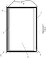
- FIG. 1depicts a conventional dynamic IGU 100 in which a bus bar 101 runs underneath a seal 102 in order to provide an electrical connection to an Electrochromic (EC) coating layer 103.
- Bus bar 101creates an electrical contact path to a top conducting layer (not indicated) formed on EC coating layer 103. The electrical path is completed through the stack of the electrochromic device to a bottom conductive layer 104 and then to a second bus bar 105 that is outside seal 102.
- Second bus bar 105is connected back to a voltage source 106.
- Bus bar 101allows an electrical contact to be made to the top of EC coating layer 103 from outside the sealed volume of IGU 100.
- EC coating layer 103is too delicate for seal 102 to be attached directly to EC coating layer 103 so EC coating layer 103 cannot extend underneath and be available for electrical contact.
- FIG. 2is a Pareto chart depicting a typical EC Absorptive Window Failure Mode Effects Analysis FMEA in a finished IGU product.
- Figure 2shows that failure of the primary seal at the bus bar is one of the highest risk reliability failure modes in a finished IGU product. Accordingly, if the breaching of the seal by the bus bar could be eliminated, one of the highest risk reliability failure modes in a finished IGU product could be eliminated.
- exemplarymeans “serving as an example, instance, or illustration.” Any embodiment described herein as “exemplary” is not to be construed as necessarily preferred or advantageous over other embodiments.
- bus barscan take up shapes on more of the perimeter of the coating inside the volume which enhances performance of the electrical operation of the electrochromic (EC) stack.
- Figures 3A-3Edepict a sequence of a technique for producing a dynamic IGU comprising a bus bar that provides an electrical connection to an Electrochromic (EC) stack without breaching the seal of the IGU according to the subject matter disclosed herein.
- Figure 3Adepicts a transparent substrate that has been coated in a well-known manner with a transparent conductive material layer 301.
- Suitable materials for conductive material layer 301include, for example, fluorine-doped tin oxide (SnO 2 :F, also abbreviated as FTO), Indium Tin Oxide (ITO), 80-90 % indium oxide with a minor amount of ITO, and aluminum doped ZnO (ZnO:Al), sometimes abbreviated as AZO.
- Transparent conductive material layer 301is formed into two electrically isolated zones, zones 301a and 301b, using a well-known technique, such as laser ablation to scribe an isolation line 302. Both conductive zones 301a and 301b on the substrate will act as a bus bar that passes beneath the primary seal thereby keeping the primary seal intact and eliminating one of the highest risk reliability failure modes in a finished conventional IGU product.
- an electrochromic stackis formed in a well-known manner on conductive material layer 301 in zone 301b so that stack 303 overlaps isolation line 302.
- a second transparent conductive material layer 303is formed in a well-known manner on the electrochromic stack so that the second transparent conductive layer 303 overlaps isolation line 302.
- the electrochromic stackis not shown in Figures 3B-3E for clarity, but it should be understood that the electrochromic stack is underneath second transparent conductive layer 303, as viewed in Figures 3B-3E .
- Suitable materials for second conductive material layer 303include, for example, FTO, ITO and AZO.
- electrochromic stackcomprises a counter electrode (CE) layer formed in a well-known manner on conductive material layer 301, an ion conductor (IC) layer formed in a well-known manner on the CE layer, and an electrochromic (EC) layer formed on the IC layer.
- electrochromic stackcomprises an electrochromic (EC) layer formed in a well-known manner on conductive material layer 301, an ion conductor (IC) layer formed in a well-known manner on the EC layer, and a counter electrode (CE) layer formed on the IC layer.
- Both exemplary embodiments of electrochromic stack 303can be formed from well-known materials that are used for forming electrochromic stacks.
- a bus bar 304is formed in a well-known manner, such as by ultrasonic soldering, so that it overlaps the edge of transparent coating 301 of zone 301a and to overlap edges of second transparent conductive layer 303 that overlaps zone 301a.
- Bus bar 304is formed so that it will be within the sealed volume of the resulting IGU.
- Bus bar 304when formed, shorts through the electrochromic stack, thereby creating a conductive path between first conductive material layer 301 and second conductive material layer 304. The short created when bus 304 is formed is in zone 301a so that the short is isolated from the operational portion of the electrochromic stack in zone 301b.
- a terminal contact 305is formed in a well-known manner on transparent coating 301 in zone 301a in a place that will be outside of the sealed volume of the resulting IGU.
- the position, size and shape of terminal contact 305is selected so that terminal contact 305 does not come into contact with and/or compromise the integrity of the seal (seal 307 in Figure 3D ) of the IGU.
- a bus bar 306is formed in a well-known manner on transparent coating 301 in zone 301b in a place that will be outside of the sealed volume of the resulting IGU.
- Suitable materials for bus bars 304 and 306include, for example, silver frit/fired paste and ultrasonic solder of various types.
- a primary seal 307is formed in a well-known manner on zones 301a and 301b so that bus bar 304 is entirely within the sealed volume and bus bar 306 is outside the sealed volume.
- a suitable material for primary seal 307is polyisobutylene.
- the IGUis finalized by trimming the substrate in a well-known manner.
- a voltage source 308is connected to terminal contacts 305 and bus bar 306 to control in a well-known manner the transparency/reflectivity of the dynamic IGU.
- the exemplary embodiments disclosed hereinare formed with two electrically isolated zones, it should be understood that more than two electrically isolated zones could be formed for a multi-zone dynamic IGU. Additionally, while the exemplary embodiments disclosed herein are formed so that the two conductive material layers cover substantially the same area as the electrochromic stack, it should be understood that at least one conductive material layer could be formed to cover an area that is substantially different from the area of the electrochromic stack. Further, an alternative exemplary embodiment provides that the electrochromic stack is formed so that it does not overlap the isolation line. For this alternative exemplary embodiment, an additional masking step is required to keep the electrochromic stack from overlapping the isolation line, while the second (or top) transparent conductive layer overlaps the isolation line. Yet another exemplary embodiment provides that the electrochromic stack overlaps one or more selected portions of the isolation line.
Landscapes
- Engineering & Computer Science (AREA)
- Structural Engineering (AREA)
- Chemical & Material Sciences (AREA)
- Architecture (AREA)
- Civil Engineering (AREA)
- Life Sciences & Earth Sciences (AREA)
- Chemical Kinetics & Catalysis (AREA)
- General Chemical & Material Sciences (AREA)
- Geochemistry & Mineralogy (AREA)
- Materials Engineering (AREA)
- Organic Chemistry (AREA)
- Electrochromic Elements, Electrophoresis, Or Variable Reflection Or Absorption Elements (AREA)
Description
- The subject matter disclosed herein relates to dynamic windows, such as smart windows. More particularly, the subject matter disclosed herein relates to a technique for making electrical contact within a dynamic Insulated Glass Unit (IGU) window assembly.
- For a conventional dynamic IGU, the transparent conducting layer of an electrochromic pane is semi-hermetically sealed within the IGU and electrical contact must be made between the transparent conducting layer and the exterior of the sealed IGU. Conventional techniques for making the electrical contact involve using a fired, silk screened or soldered bus bar.
Figure 1 depicts a conventionaldynamic IGU 100 in which abus bar 101 runs underneath aseal 102 in order to provide an electrical connection to an Electrochromic (EC)coating layer 103.Bus bar 101 creates an electrical contact path to a top conducting layer (not indicated) formed onEC coating layer 103. The electrical path is completed through the stack of the electrochromic device to a bottomconductive layer 104 and then to asecond bus bar 105 that is outsideseal 102.Second bus bar 105 is connected back to avoltage source 106.Bus bar 101 allows an electrical contact to be made to the top ofEC coating layer 103 from outside the sealed volume of IGU 100.EC coating layer 103 is too delicate forseal 102 to be attached directly toEC coating layer 103 soEC coating layer 103 cannot extend underneath and be available for electrical contact. - The breaching of
seal 102 bybus bar 101 reduces the reliability ofseal 102.Figure 2 is a Pareto chart depicting a typical EC Absorptive Window Failure Mode Effects Analysis FMEA in a finished IGU product.Figure 2 shows that failure of the primary seal at the bus bar is one of the highest risk reliability failure modes in a finished IGU product. Accordingly, if the breaching of the seal by the bus bar could be eliminated, one of the highest risk reliability failure modes in a finished IGU product could be eliminated. - The subject matter disclosed herein is illustrated by way of example and not by limitation in the accompanying figures in which like reference numerals indicate similar elements and in which:
Figure 1 depicts a conventional dynamic IGU in which a bus bar breaches a seal in order to provide an electrical connection to an Electrochromic (EC) coating layer;Figure 2 is a Pareto chart depicting a typical EC Absorptive Window Failure Mode Effects Analysis (FMEA) in a finished IGU product; andFigures 3A-3E depict a sequence of a technique for producing a dynamic IGU comprising a bus bar that provides an electrical connection to an Electrochromic (EC) coating layer without breaching the seal of the IGU according to the subject matter disclosed herein.- As used herein, the word "exemplary" means "serving as an example, instance, or illustration." Any embodiment described herein as "exemplary" is not to be construed as necessarily preferred or advantageous over other embodiments.
- The subject matter disclosed eliminates a bus bar from running underneath the seal which, in turn, eliminates one of the highest risk reliability failure modes in a finished IGU product by utilizing a conducting substrate as a contact path for control signals in place of a conventional bus bar. Another benefit of the subject matter disclosed herein is that bus bars can take up shapes on more of the perimeter of the coating inside the volume which enhances performance of the electrical operation of the electrochromic (EC) stack.
Figures 3A-3E depict a sequence of a technique for producing a dynamic IGU comprising a bus bar that provides an electrical connection to an Electrochromic (EC) stack without breaching the seal of the IGU according to the subject matter disclosed herein.Figure 3A depicts a transparent substrate that has been coated in a well-known manner with a transparentconductive material layer 301. Suitable materials forconductive material layer 301 include, for example, fluorine-doped tin oxide (SnO2:F, also abbreviated as FTO), Indium Tin Oxide (ITO), 80-90 % indium oxide with a minor amount of ITO, and aluminum doped ZnO (ZnO:Al), sometimes abbreviated as AZO. The transparent substrate has not been indicated for clarity. It should be understood that the transparent substrate could be glass, acrylic or polycarbonate. Transparentconductive material layer 301 is formed into two electrically isolated zones,zones isolation line 302. Bothconductive zones - In
Figure 3B , an electrochromic stack is formed in a well-known manner onconductive material layer 301 inzone 301b so thatstack 303overlaps isolation line 302. A second transparentconductive material layer 303 is formed in a well-known manner on the electrochromic stack so that the second transparentconductive layer 303overlaps isolation line 302. (The electrochromic stack is not shown inFigures 3B-3E for clarity, but it should be understood that the electrochromic stack is underneath second transparentconductive layer 303, as viewed inFigures 3B-3E .) Suitable materials for secondconductive material layer 303 include, for example, FTO, ITO and AZO. In one exemplary embodiment shown inFigures 3B-3E , electrochromic stack comprises a counter electrode (CE) layer formed in a well-known manner onconductive material layer 301, an ion conductor (IC) layer formed in a well-known manner on the CE layer, and an electrochromic (EC) layer formed on the IC layer. In another exemplary embodiment, electrochromic stack comprises an electrochromic (EC) layer formed in a well-known manner onconductive material layer 301, an ion conductor (IC) layer formed in a well-known manner on the EC layer, and a counter electrode (CE) layer formed on the IC layer. Both exemplary embodiments ofelectrochromic stack 303 can be formed from well-known materials that are used for forming electrochromic stacks. - In
Figure 3C , abus bar 304 is formed in a well-known manner, such as by ultrasonic soldering, so that it overlaps the edge oftransparent coating 301 ofzone 301a and to overlap edges of second transparentconductive layer 303 that overlapszone 301a.Bus bar 304 is formed so that it will be within the sealed volume of the resulting IGU.Bus bar 304, when formed, shorts through the electrochromic stack, thereby creating a conductive path between firstconductive material layer 301 and secondconductive material layer 304. The short created whenbus 304 is formed is inzone 301a so that the short is isolated from the operational portion of the electrochromic stack inzone 301b. Aterminal contact 305 is formed in a well-known manner ontransparent coating 301 inzone 301a in a place that will be outside of the sealed volume of the resulting IGU. The position, size and shape ofterminal contact 305 is selected so thatterminal contact 305 does not come into contact with and/or compromise the integrity of the seal (seal 307 inFigure 3D ) of the IGU. Abus bar 306 is formed in a well-known manner ontransparent coating 301 inzone 301b in a place that will be outside of the sealed volume of the resulting IGU. Suitable materials forbus bars - In
Figure 3D , aprimary seal 307 is formed in a well-known manner onzones bus bar 304 is entirely within the sealed volume andbus bar 306 is outside the sealed volume. A suitable material forprimary seal 307 is polyisobutylene. InFigure 3E , the IGU is finalized by trimming the substrate in a well-known manner. Avoltage source 308 is connected toterminal contacts 305 andbus bar 306 to control in a well-known manner the transparency/reflectivity of the dynamic IGU. - While the exemplary embodiments disclosed herein are formed with two electrically isolated zones, it should be understood that more than two electrically isolated zones could be formed for a multi-zone dynamic IGU. Additionally, while the exemplary embodiments disclosed herein are formed so that the two conductive material layers cover substantially the same area as the electrochromic stack, it should be understood that at least one conductive material layer could be formed to cover an area that is substantially different from the area of the electrochromic stack. Further, an alternative exemplary embodiment provides that the electrochromic stack is formed so that it does not overlap the isolation line. For this alternative exemplary embodiment, an additional masking step is required to keep the electrochromic stack from overlapping the isolation line, while the second (or top) transparent conductive layer overlaps the isolation line. Yet another exemplary embodiment provides that the electrochromic stack overlaps one or more selected portions of the isolation line.
- Although the foregoing disclosed subject matter has been described in some detail for purposes of clarity of understanding, it will be apparent that certain changes and modifications may be practiced that are within the scope of the appended claims. Accordingly, the present embodiments are to be considered as illustrative and not restrictive, and the subject matter disclosed herein is not to be limited to the details given herein, but may be modified within the scope of the appended claims.
Claims (16)
- A dynamic Insulating Glass Unit (IGU) window assembly, comprising:a first conductive material layer formed on a substrate, the first conductive material layer comprising at least two zones that are each electrically isolated from each other;an electrochromic stack formed on at least a portion of a first selected zone of the first conductive material layer;a second conductive material layer formed on at least a portion of the electrochromic stack to overlap and electrically contact at least an edge of a second selected zone of the first conductive material layer without making any electrical contact with the first zone of the first conductive material layer;a first bus bar formed directly on the second selected zone of the first conductive material layer, which also electrically contacts the second conductive material layer without electrically contacting the first zone of the first conductive material layer, the first bus bar being located entirely within a sealed volume of the window assembly;and a second bus bar formed directly on the first selected zone, the second bus bar being located entirely outside the sealed volume of the window assembly.
- The window assembly according to claim 1, further comprising a seal defining the sealed volume of the window assembly.
- The window assembly according to claim 1, wherein the electrochromic stack comprises:a counter electrode (CE) layer formed on the first conductive material layer in the first selected zone of the first conductive material layer;an ion conductor (IC) layer formed on the counter electrode (CE) layer; andan electrochromic (EC) layer formed on the ion conductor (IC) layer.
- The window assembly according to claim 3, wherein the second conductive material layer is formed on the electrochromic (EC) layer of the electrochromic stack.
- The window assembly according to claim 4, further comprising a seal defining the sealed volume of the window assembly.
- The window assembly according to claim 1, wherein the electrochromic stack comprises:an electrochromic (EC) layer formed on the first conductive material layer in the first selected zone of the first conductive material layer;an ion conductor (IC) layer formed on the electrochromic (EC) layer; andan counter electrode (CE) layer formed on the ion conductor (IC) layer.
- The window assembly according to claim 6, wherein the second conductive material layer is formed on the electrochromic (EC) layer of the electrochromic stack.
- The window assembly according to claim 7, further comprising a seal defining the sealed volume of the window assembly.
- A window assembly according to any one of claims 1-8, wherein said electrochromic stack is formed on the first selected zone of the first conductive material layer to overlap at least an edge of the second selected zone of the first conductive material layer.
- A method, comprising:forming a first conductive material layer formed on a substrate, the first conductive material layer comprising at least two zones that are each electrically isolated from each other;forming an electrochromic stack on a first selected zone of the first conductive material layer to overlap at least an edge of a second selected zone of the first conductive material layer;forming a second conductive material layer on at least a portion of the electrochromic stack to overlap and electrically contact at least an edge of the second selected zone of the first conductive material layer without making any electrical contact with the first zone of the first conductive material layer;forming a first bus bar directly on the second selected zone of the first conductive material layer, which also electrically contacts the second conductive material layer without electrically contacting the first zone of the first conductive material layer, the first bus bar being located entirely within a sealed volume of the window assembly; andforming a second bus bar directly on the first selected zone, the second bus bar being located entirely outside the sealed volume of the window assembly.
- The method according to claim 10, further comprising forming a seal defining the sealed volume of the window assembly.
- The method according to claim 10, wherein forming the electrochromic stack comprises:forming a counter electrode (CE) layer on the first conductive material layer in the first selected zone of the first conductive material layer;forming an ion conductor (IC) layer on the counter electrode (CE) layer; andforming an electrochromic (EC) layer on the ion conductor (IC) layer.
- The method according to claim 12, wherein forming the second conductive material layer comprises forming the second conductive material layer on the electrochromic (EC) layer of the electrochromic stack.
- The method according to claim 13, further comprising forming a seal defining the sealed volume of the window assembly.
- The method according to claim 10, wherein forming the electrochromic stack comprises:forming an electrochromic (EC) layer on the first conductive material layer in the first selected zone of the first conductive material layer;forming an ion conductor (IC) layer on the electrochromic (EC) layer; andforming a counter electrode (CE) layer on the ion conductor (IC) layer.
- The method according to claim 15, wherein forming the second conductive material layer comprises forming the second conductive material layer on the electrochromic (EC) layer of the electrochromic stack.
Applications Claiming Priority (2)
| Application Number | Priority Date | Filing Date | Title |
|---|---|---|---|
| US12/212,482US7719751B2 (en) | 2008-09-17 | 2008-09-17 | Electrical contact technique for electrochromic windows |
| PCT/US2009/056928WO2010033485A2 (en) | 2008-09-17 | 2009-09-15 | Electrical contact technique for electrochromic window |
Publications (3)
| Publication Number | Publication Date |
|---|---|
| EP2349939A2 EP2349939A2 (en) | 2011-08-03 |
| EP2349939A4 EP2349939A4 (en) | 2015-07-29 |
| EP2349939B1true EP2349939B1 (en) | 2018-11-28 |
Family
ID=42006983
Family Applications (1)
| Application Number | Title | Priority Date | Filing Date |
|---|---|---|---|
| EP09815048.5ANot-in-forceEP2349939B1 (en) | 2008-09-17 | 2009-09-15 | Electrical contact technique for electrochromic window |
Country Status (3)
| Country | Link |
|---|---|
| US (1) | US7719751B2 (en) |
| EP (1) | EP2349939B1 (en) |
| WO (1) | WO2010033485A2 (en) |
Families Citing this family (53)
| Publication number | Priority date | Publication date | Assignee | Title |
|---|---|---|---|---|
| US8514476B2 (en) | 2008-06-25 | 2013-08-20 | View, Inc. | Multi-pane dynamic window and method for making same |
| US9664974B2 (en)* | 2009-03-31 | 2017-05-30 | View, Inc. | Fabrication of low defectivity electrochromic devices |
| US10303035B2 (en) | 2009-12-22 | 2019-05-28 | View, Inc. | Self-contained EC IGU |
| US9958750B2 (en)* | 2010-11-08 | 2018-05-01 | View, Inc. | Electrochromic window fabrication methods |
| WO2012078634A2 (en) | 2010-12-08 | 2012-06-14 | Soladigm, Inc. | Improved spacers for insulated glass units |
| US10180606B2 (en) | 2010-12-08 | 2019-01-15 | View, Inc. | Connectors for smart windows |
| US9442339B2 (en) | 2010-12-08 | 2016-09-13 | View, Inc. | Spacers and connectors for insulated glass units |
| US8643933B2 (en) | 2011-12-14 | 2014-02-04 | View, Inc. | Connectors for smart windows |
| US9454055B2 (en) | 2011-03-16 | 2016-09-27 | View, Inc. | Multipurpose controller for multistate windows |
| US10175549B2 (en) | 2011-03-16 | 2019-01-08 | View, Inc. | Connectors for smart windows |
| US10429712B2 (en) | 2012-04-20 | 2019-10-01 | View, Inc. | Angled bus bar |
| CN103562788A (en)* | 2011-05-26 | 2014-02-05 | 赛智电致变色公司 | Bridged bus bar for electrochromic devices |
| US11865632B2 (en) | 2011-12-12 | 2024-01-09 | View, Inc. | Thin-film devices and fabrication |
| US10802371B2 (en) | 2011-12-12 | 2020-10-13 | View, Inc. | Thin-film devices and fabrication |
| US10295880B2 (en) | 2011-12-12 | 2019-05-21 | View, Inc. | Narrow pre-deposition laser deletion |
| US12403676B2 (en) | 2011-12-12 | 2025-09-02 | View Operating Corporation | Thin-film devices and fabrication |
| CN104011588B (en) | 2011-12-12 | 2021-06-22 | 唯景公司 | Thin Film Devices and Manufacturing |
| US12061402B2 (en) | 2011-12-12 | 2024-08-13 | View, Inc. | Narrow pre-deposition laser deletion |
| US11719039B2 (en) | 2011-12-14 | 2023-08-08 | View, Inc. | Connectors for smart windows |
| US11635666B2 (en) | 2012-03-13 | 2023-04-25 | View, Inc | Methods of controlling multi-zone tintable windows |
| US9341912B2 (en) | 2012-03-13 | 2016-05-17 | View, Inc. | Multi-zone EC windows |
| US12153320B2 (en) | 2012-03-13 | 2024-11-26 | View, Inc. | Multi-zone EC windows |
| US12429742B2 (en) | 2012-03-13 | 2025-09-30 | View Operating Corporation | Methods of controlling multi-zone tintable windows |
| US11255120B2 (en) | 2012-05-25 | 2022-02-22 | View, Inc. | Tester and electrical connectors for insulated glass units |
| JP2015527279A (en)* | 2012-06-05 | 2015-09-17 | セイジ・エレクトロクロミクス,インコーポレイテッド | Electrical feedthrough spacer and connectivity |
| EP2888427B1 (en) | 2012-08-23 | 2021-02-17 | View, Inc. | Photonic-powered electrochromic (ec) devices |
| US9684218B2 (en) | 2012-11-07 | 2017-06-20 | University Of South Florida | Low-cost chromatic devices |
| US9158172B2 (en) | 2012-11-14 | 2015-10-13 | Sage Electrochromics, Inc. | Color matched coating for bus bars |
| CA2846049A1 (en)* | 2013-03-15 | 2014-09-15 | Andersen Corporation | Glazing units with cartridge-based control units |
| TWI685706B (en) | 2013-06-18 | 2020-02-21 | 唯景公司 | Electrochromic devices on non-rectangular shapes |
| WO2017112685A1 (en)* | 2015-12-21 | 2017-06-29 | View, Inc. | Obscuring bus bars in electrochromic glass structures |
| US10884311B2 (en) | 2013-12-24 | 2021-01-05 | View, Inc. | Obscuring bus bars in electrochromic glass structures |
| CN105814271B (en) | 2013-12-24 | 2019-03-22 | 唯景公司 | Masking bus bars in electrochromic glass structures |
| US11906868B2 (en) | 2013-12-24 | 2024-02-20 | View, Inc. | Obscuring bus bars in electrochromic glass structures |
| CN106537243B (en)* | 2014-07-03 | 2021-08-27 | 唯景公司 | Narrow pre-deposition laser ablation |
| US12235560B2 (en) | 2014-11-25 | 2025-02-25 | View, Inc. | Faster switching electrochromic devices |
| CN113655669B (en) | 2014-12-19 | 2025-03-04 | 唯景公司 | Reducing defects under bus bars in electrochromic devices |
| US10969645B2 (en) | 2015-03-20 | 2021-04-06 | View, Inc. | Faster switching low-defect electrochromic windows |
| CN108027542B (en)* | 2015-08-07 | 2021-08-06 | 基内斯托技术公司 | Electrochromic device components |
| CN114265251B (en) | 2016-04-19 | 2024-12-06 | Sage电致变色显示有限公司 | Electrochromic device including a transparent conductive oxide layer and a bus bar and a method of forming the same |
| WO2017218705A1 (en) | 2016-06-17 | 2017-12-21 | View, Inc. | Mitigating defects in an electrochromic device under a bus bar |
| WO2018195458A1 (en) | 2017-04-20 | 2018-10-25 | Cardinal Ig Company | High performance privacy glazing structures |
| WO2019014613A1 (en) | 2017-07-13 | 2019-01-17 | Cardinal Ig Company | Electrical connection configurations for privacy glazing structures |
| EP3682295B1 (en) | 2017-09-12 | 2023-09-06 | Sage Electrochromics, Inc. | Non-light-emitting variable transmission device and a method of forming the same |
| EP3707555B1 (en) | 2017-11-06 | 2025-05-07 | Cardinal Ig Company | Privacy glazing system with discrete electrical driver |
| MX2020011871A (en) | 2018-05-09 | 2021-01-20 | Cardinal Ig Co | Electrically controllable privacy glazing with energy recapturing driver. |
| CN112654919B (en) | 2018-08-17 | 2024-05-28 | 卡迪纳尔Ig公司 | Privacy glazing structure with asymmetric pane offset for electrical connection configuration |
| US11474385B1 (en) | 2018-12-02 | 2022-10-18 | Cardinal Ig Company | Electrically controllable privacy glazing with ultralow power consumption comprising a liquid crystal material having a light transmittance that varies in response to application of an electric field |
| WO2020163836A1 (en) | 2019-02-08 | 2020-08-13 | Cardinal Ig Company | Low power driver for privacy glazing |
| MX2021013259A (en) | 2019-04-29 | 2022-01-06 | Cardinal Ig Co | SYSTEMS AND METHODS FOR OPERATING ONE OR MORE GLAZING STRUCTURES WITH ELECTRICALLY CONTROLLABLE PRIVACY. |
| US11175523B2 (en) | 2019-04-29 | 2021-11-16 | Cardinal Ig Company | Staggered driving electrical control of a plurality of electrically controllable privacy glazing structures |
| KR102809744B1 (en) | 2019-04-29 | 2025-05-16 | 카디날 아이지 컴퍼니 | Leakage current detection and control for one or more electrically controllable privacy glass structures |
| US11703737B2 (en)* | 2020-02-12 | 2023-07-18 | Sage Electrochromics, Inc. | Forming electrochromic stacks using at most one metallic lithium deposition station |
Citations (5)
| Publication number | Priority date | Publication date | Assignee | Title |
|---|---|---|---|---|
| EP0851271A2 (en)* | 1996-12-24 | 1998-07-01 | Nippon Oil Co. Ltd. | Electrode for electrochromic device and electrochromic device |
| US6798556B2 (en)* | 2003-01-31 | 2004-09-28 | Rockwell Scientific Licensing, Llc. | Locally-switched reversible electrodeposition optical modulator |
| WO2007100921A2 (en)* | 2006-03-03 | 2007-09-07 | Gentex Corporation | Improved thin-film coatings, electro-optic elements and assemblies incorporating these elements |
| US20080074724A1 (en)* | 2003-03-05 | 2008-03-27 | Anoop Agrawal | Electrochromic Mirrors and other Electrooptic Devices |
| US20100243427A1 (en)* | 2009-03-31 | 2010-09-30 | Soladigm, Inc. | Fabrication of low defectivity electrochromic devices |
Family Cites Families (45)
| Publication number | Priority date | Publication date | Assignee | Title |
|---|---|---|---|---|
| GB2190760B (en)* | 1986-05-21 | 1990-04-18 | Nippon Kogaku Kk | Electrochromic element |
| CA1313562C (en)* | 1988-08-17 | 1993-02-09 | Nikon Corporation | Electrochromic device |
| US5151816A (en)* | 1989-12-29 | 1992-09-29 | Donnelly Corporation | Method for reducing current leakage and enhancing uv stability in electrochemichromic solutions and devices |
| US5187607A (en)* | 1989-03-13 | 1993-02-16 | Nikon Corporation | Electrochromic device with low resistance electrical connections |
| US5140455A (en)* | 1989-11-29 | 1992-08-18 | Donnelly Corporation | High performance electrochemichromic solutions and devices thereof |
| US5142407A (en)* | 1989-12-22 | 1992-08-25 | Donnelly Corporation | Method of reducing leakage current in electrochemichromic solutions and solutions based thereon |
| US5076673A (en)* | 1990-08-10 | 1991-12-31 | Donnelly Corporation | Prolonged coloration electrochromic assembly |
| US5145609A (en)* | 1990-11-07 | 1992-09-08 | Donnelly Corporation | Linear polyether-containing electrochemichromic solutions and related devices |
| US5239405A (en)* | 1991-09-06 | 1993-08-24 | Donnelly Corporation | Electrochemichromic solutions, processes for preparing and using the same, and devices manufactured with the same |
| US5500760A (en)* | 1991-09-06 | 1996-03-19 | Donnelly Corporation | Electrochemichromic solutions, processes for preparing and using the same, and devices manufactured with the same |
| US5233461A (en)* | 1991-09-06 | 1993-08-03 | Donnelly Corporation | Methods for sealing electrochromic devices and devices manufactured thereby |
| US5910854A (en)* | 1993-02-26 | 1999-06-08 | Donnelly Corporation | Electrochromic polymeric solid films, manufacturing electrochromic devices using such solid films, and processes for making such solid films and devices |
| EP0612826B1 (en) | 1993-02-26 | 2000-10-04 | Donnelly Corporation | Electrochromic polymeric solid films, manufacturing electrochromic devices using such solid films, and processing for making such solid films and devices |
| US5471338A (en) | 1993-11-12 | 1995-11-28 | Ppg Industries, Inc. | Electrochromic device with plastic substrate |
| US5668663A (en)* | 1994-05-05 | 1997-09-16 | Donnelly Corporation | Electrochromic mirrors and devices |
| JP3439014B2 (en)* | 1996-02-29 | 2003-08-25 | 三洋電機株式会社 | Liquid crystal display |
| US5805330A (en)* | 1996-03-15 | 1998-09-08 | Gentex Corporation | Electro-optic window incorporating a discrete photovoltaic device |
| US6433913B1 (en)* | 1996-03-15 | 2002-08-13 | Gentex Corporation | Electro-optic device incorporating a discrete photovoltaic device and method and apparatus for making same |
| US5995271A (en)* | 1997-10-07 | 1999-11-30 | Optical Coating Laboratory, Inc. | Protective coating materials for electrochromic devices |
| US5969847A (en)* | 1997-12-22 | 1999-10-19 | Ppg Industries Ohio, Inc. | Method for sealing a laminated electrochromic device edge |
| US5953150A (en)* | 1997-12-22 | 1999-09-14 | Ppg Industries Ohio, Inc. | Edge design for electrochromic devices |
| JP3932642B2 (en)* | 1998-01-23 | 2007-06-20 | トヨタ自動車株式会社 | Exhaust gas purification device for lean combustion internal combustion engine |
| JP2000002895A (en)* | 1998-04-14 | 2000-01-07 | Murakami Corp | Sealing structure of all solid type electrochromic antidazzle mirror |
| US6166849A (en)* | 1998-12-15 | 2000-12-26 | Ppg Industries Ohio, Inc. | Aromatic glycidyl amine-based epoxy edge seals for electrooptic devices |
| US6055089A (en)* | 1999-02-25 | 2000-04-25 | Minnesota Mining And Manufacturing Company | Photovoltaic powering and control system for electrochromic windows |
| US6244716B1 (en)* | 1999-05-17 | 2001-06-12 | Gentex Corporation | Exterior mirror sub-assembly with combined electronic circuitry and mirror element |
| US7324261B2 (en)* | 1999-07-09 | 2008-01-29 | Gentex Corporation | Electrochromic devices with thin bezel-covered edge |
| US6515787B1 (en)* | 2000-03-07 | 2003-02-04 | Eclipse Energy Systems, Inc. | Electrochromic layer |
| WO2001084230A1 (en)* | 2000-05-04 | 2001-11-08 | Schott Donnelly Llc | Chromogenic glazing |
| US6561460B2 (en)* | 2000-08-03 | 2003-05-13 | Ppg Industries Ohio, Inc. | Switchable electrochromic devices for use in aircraft transparency windows |
| US6471360B2 (en)* | 2000-08-03 | 2002-10-29 | Ppg Industries Ohio, Inc. | Switchable electrochromic devices with uniform switching and preferential area shading |
| EP1333316A4 (en)* | 2000-11-10 | 2004-04-07 | Murakami Corp | Solid state electrochromic element and mirror device and crt display comprising it |
| US6535126B2 (en)* | 2000-12-15 | 2003-03-18 | Ppg Industries Ohio, Inc. | Electrochromic transparency incorporating security system |
| US6639708B2 (en)* | 2001-04-24 | 2003-10-28 | Schott North America, Inc | Electrochromic safety glazing |
| US7832177B2 (en)* | 2002-03-22 | 2010-11-16 | Electronics Packaging Solutions, Inc. | Insulated glazing units |
| US6961168B2 (en)* | 2002-06-21 | 2005-11-01 | The Regents Of The University Of California | Durable electrooptic devices comprising ionic liquids |
| CN100386691C (en)* | 2002-06-21 | 2008-05-07 | 洛斯阿拉莫斯国家安全股份有限公司 | Electrooptical device containing ionic liquid, electrooptical automobile mirror and electrolyte used for electrooptical device and electrooptical automobile mirror |
| JP4101864B2 (en)* | 2002-11-18 | 2008-06-18 | 株式会社村上開明堂 | Solid EC element |
| US6862125B2 (en)* | 2003-05-05 | 2005-03-01 | The Regents Of The University Of California | Reversible electro-optic device employing aprotic molten salts and method |
| US7133181B2 (en)* | 2004-07-23 | 2006-11-07 | Sage Electrochromics, Inc. | Control system for electrochromic devices |
| US7248392B2 (en)* | 2005-07-01 | 2007-07-24 | Ppg Industries Ohio, Inc. | Vision panel having a multi-layer primer |
| US7173750B2 (en)* | 2005-07-01 | 2007-02-06 | Ppg Industries Ohio, Inc. | Electrochromic vision panel having a plurality of connectors |
| US7586664B2 (en)* | 2005-07-01 | 2009-09-08 | Ppg Industries Ohio, Inc. | Transparent electrode for an electrochromic switchable cell |
| US7362491B2 (en)* | 2006-02-10 | 2008-04-22 | Radiant Glass Industries, Llc | Heated glass panels and methods for making electrical contact with electro-conductive films |
| US7645977B2 (en)* | 2006-11-17 | 2010-01-12 | New Visual Media Group, L.L.C. | Low cost dynamic insulated glazing unit |
- 2008
- 2008-09-17USUS12/212,482patent/US7719751B2/enactiveActive
- 2009
- 2009-09-15WOPCT/US2009/056928patent/WO2010033485A2/enactiveApplication Filing
- 2009-09-15EPEP09815048.5Apatent/EP2349939B1/ennot_activeNot-in-force
Patent Citations (5)
| Publication number | Priority date | Publication date | Assignee | Title |
|---|---|---|---|---|
| EP0851271A2 (en)* | 1996-12-24 | 1998-07-01 | Nippon Oil Co. Ltd. | Electrode for electrochromic device and electrochromic device |
| US6798556B2 (en)* | 2003-01-31 | 2004-09-28 | Rockwell Scientific Licensing, Llc. | Locally-switched reversible electrodeposition optical modulator |
| US20080074724A1 (en)* | 2003-03-05 | 2008-03-27 | Anoop Agrawal | Electrochromic Mirrors and other Electrooptic Devices |
| WO2007100921A2 (en)* | 2006-03-03 | 2007-09-07 | Gentex Corporation | Improved thin-film coatings, electro-optic elements and assemblies incorporating these elements |
| US20100243427A1 (en)* | 2009-03-31 | 2010-09-30 | Soladigm, Inc. | Fabrication of low defectivity electrochromic devices |
Also Published As
| Publication number | Publication date |
|---|---|
| EP2349939A4 (en) | 2015-07-29 |
| US20100067090A1 (en) | 2010-03-18 |
| US7719751B2 (en) | 2010-05-18 |
| EP2349939A2 (en) | 2011-08-03 |
| WO2010033485A3 (en) | 2010-07-01 |
| WO2010033485A2 (en) | 2010-03-25 |
Similar Documents
| Publication | Publication Date | Title |
|---|---|---|
| EP2349939B1 (en) | Electrical contact technique for electrochromic window | |
| CN102209830B (en) | Switchable glazings | |
| US8405896B2 (en) | Controlled-transparency electrochromic device | |
| US8289609B2 (en) | Controlled-transparency electrochromic device | |
| CN108027542B (en) | Electrochromic device components | |
| US9482921B2 (en) | Electrochromic device | |
| CN104011588B (en) | Thin Film Devices and Manufacturing | |
| KR20080108110A (en) | Laminated glazing and their seals and peripheral reinforcement means | |
| JP5400273B2 (en) | Dye-sensitized solar cell and composite device including the same | |
| TW201825994A (en) | Method and system for fabricating electrochromic devices | |
| JP2023537984A (en) | Insulating glazing units with electrically conductive coatings and/or electrically controllable functional elements | |
| US20240052688A1 (en) | Connecting element for insulated glazing with an electrically conductive coating and/or electrically controllable functional element | |
| JPH0983001A (en) | Integrated thin film solar battery | |
| CN210803935U (en) | Dimming glass and smart windows | |
| JP2021521093A (en) | Long busbar with segments for increased robustness | |
| US20230121640A1 (en) | Laminated glazing with electrically connected layer and method of preparing a laminated glazing | |
| CN211786487U (en) | PDLC light modulation film | |
| HK1160100A (en) | Electrical contact technique for electrochromic window | |
| HK1160100B (en) | Electrical contact technique for electrochromic window | |
| US8642166B2 (en) | Transparent conductive thin film | |
| KR102393605B1 (en) | Electrochromic apparatus | |
| JPH055536Y2 (en) | ||
| TWI815164B (en) | Disc with functional element with electrically switchable optical properties and pattern for high-frequency transmission | |
| JPH1122332A (en) | Double glazing | |
| JPH0820648B2 (en) | EC device with extraction electrodes on the end face |
Legal Events
| Date | Code | Title | Description |
|---|---|---|---|
| PUAI | Public reference made under article 153(3) epc to a published international application that has entered the european phase | Free format text:ORIGINAL CODE: 0009012 | |
| 17P | Request for examination filed | Effective date:20110415 | |
| AK | Designated contracting states | Kind code of ref document:A2 Designated state(s):AT BE BG CH CY CZ DE DK EE ES FI FR GB GR HR HU IE IS IT LI LT LU LV MC MK MT NL NO PL PT RO SE SI SK SM TR | |
| DAX | Request for extension of the european patent (deleted) | ||
| REG | Reference to a national code | Ref country code:HK Ref legal event code:DE Ref document number:1160100 Country of ref document:HK | |
| RAP1 | Party data changed (applicant data changed or rights of an application transferred) | Owner name:EGERTON, PETER Owner name:GASKELL, DREW Owner name:VIEW, INC. | |
| A4 | Supplementary search report drawn up and despatched | Effective date:20150625 | |
| RIC1 | Information provided on ipc code assigned before grant | Ipc:G02F 1/155 20060101ALI20150619BHEP Ipc:E06B 9/24 20060101ALI20150619BHEP Ipc:C03C 17/34 20060101AFI20150619BHEP | |
| GRAP | Despatch of communication of intention to grant a patent | Free format text:ORIGINAL CODE: EPIDOSNIGR1 | |
| STAA | Information on the status of an ep patent application or granted ep patent | Free format text:STATUS: GRANT OF PATENT IS INTENDED | |
| GRAJ | Information related to disapproval of communication of intention to grant by the applicant or resumption of examination proceedings by the epo deleted | Free format text:ORIGINAL CODE: EPIDOSDIGR1 | |
| GRAP | Despatch of communication of intention to grant a patent | Free format text:ORIGINAL CODE: EPIDOSNIGR1 | |
| INTG | Intention to grant announced | Effective date:20180327 | |
| INTG | Intention to grant announced | Effective date:20180419 | |
| GRAJ | Information related to disapproval of communication of intention to grant by the applicant or resumption of examination proceedings by the epo deleted | Free format text:ORIGINAL CODE: EPIDOSDIGR1 | |
| STAA | Information on the status of an ep patent application or granted ep patent | Free format text:STATUS: REQUEST FOR EXAMINATION WAS MADE | |
| INTC | Intention to grant announced (deleted) | ||
| GRAR | Information related to intention to grant a patent recorded | Free format text:ORIGINAL CODE: EPIDOSNIGR71 | |
| GRAS | Grant fee paid | Free format text:ORIGINAL CODE: EPIDOSNIGR3 | |
| STAA | Information on the status of an ep patent application or granted ep patent | Free format text:STATUS: GRANT OF PATENT IS INTENDED | |
| GRAA | (expected) grant | Free format text:ORIGINAL CODE: 0009210 | |
| STAA | Information on the status of an ep patent application or granted ep patent | Free format text:STATUS: THE PATENT HAS BEEN GRANTED | |
| INTG | Intention to grant announced | Effective date:20181018 | |
| AK | Designated contracting states | Kind code of ref document:B1 Designated state(s):AT BE BG CH CY CZ DE DK EE ES FI FR GB GR HR HU IE IS IT LI LT LU LV MC MK MT NL NO PL PT RO SE SI SK SM TR | |
| REG | Reference to a national code | Ref country code:GB Ref legal event code:FG4D | |
| REG | Reference to a national code | Ref country code:CH Ref legal event code:EP | |
| REG | Reference to a national code | Ref country code:AT Ref legal event code:REF Ref document number:1070025 Country of ref document:AT Kind code of ref document:T Effective date:20181215 | |
| REG | Reference to a national code | Ref country code:DE Ref legal event code:R096 Ref document number:602009055953 Country of ref document:DE | |
| REG | Reference to a national code | Ref country code:IE Ref legal event code:FG4D | |
| REG | Reference to a national code | Ref country code:NL Ref legal event code:MP Effective date:20181128 | |
| REG | Reference to a national code | Ref country code:LT Ref legal event code:MG4D | |
| REG | Reference to a national code | Ref country code:AT Ref legal event code:MK05 Ref document number:1070025 Country of ref document:AT Kind code of ref document:T Effective date:20181128 | |
| PG25 | Lapsed in a contracting state [announced via postgrant information from national office to epo] | Ref country code:NO Free format text:LAPSE BECAUSE OF FAILURE TO SUBMIT A TRANSLATION OF THE DESCRIPTION OR TO PAY THE FEE WITHIN THE PRESCRIBED TIME-LIMIT Effective date:20190228 Ref country code:LT Free format text:LAPSE BECAUSE OF FAILURE TO SUBMIT A TRANSLATION OF THE DESCRIPTION OR TO PAY THE FEE WITHIN THE PRESCRIBED TIME-LIMIT Effective date:20181128 Ref country code:AT Free format text:LAPSE BECAUSE OF FAILURE TO SUBMIT A TRANSLATION OF THE DESCRIPTION OR TO PAY THE FEE WITHIN THE PRESCRIBED TIME-LIMIT Effective date:20181128 Ref country code:BG Free format text:LAPSE BECAUSE OF FAILURE TO SUBMIT A TRANSLATION OF THE DESCRIPTION OR TO PAY THE FEE WITHIN THE PRESCRIBED TIME-LIMIT Effective date:20190228 Ref country code:HR Free format text:LAPSE BECAUSE OF FAILURE TO SUBMIT A TRANSLATION OF THE DESCRIPTION OR TO PAY THE FEE WITHIN THE PRESCRIBED TIME-LIMIT Effective date:20181128 Ref country code:LV Free format text:LAPSE BECAUSE OF FAILURE TO SUBMIT A TRANSLATION OF THE DESCRIPTION OR TO PAY THE FEE WITHIN THE PRESCRIBED TIME-LIMIT Effective date:20181128 Ref country code:FI Free format text:LAPSE BECAUSE OF FAILURE TO SUBMIT A TRANSLATION OF THE DESCRIPTION OR TO PAY THE FEE WITHIN THE PRESCRIBED TIME-LIMIT Effective date:20181128 Ref country code:IS Free format text:LAPSE BECAUSE OF FAILURE TO SUBMIT A TRANSLATION OF THE DESCRIPTION OR TO PAY THE FEE WITHIN THE PRESCRIBED TIME-LIMIT Effective date:20190328 Ref country code:ES Free format text:LAPSE BECAUSE OF FAILURE TO SUBMIT A TRANSLATION OF THE DESCRIPTION OR TO PAY THE FEE WITHIN THE PRESCRIBED TIME-LIMIT Effective date:20181128 | |
| PG25 | Lapsed in a contracting state [announced via postgrant information from national office to epo] | Ref country code:GR Free format text:LAPSE BECAUSE OF FAILURE TO SUBMIT A TRANSLATION OF THE DESCRIPTION OR TO PAY THE FEE WITHIN THE PRESCRIBED TIME-LIMIT Effective date:20190301 Ref country code:PT Free format text:LAPSE BECAUSE OF FAILURE TO SUBMIT A TRANSLATION OF THE DESCRIPTION OR TO PAY THE FEE WITHIN THE PRESCRIBED TIME-LIMIT Effective date:20190328 Ref country code:SE Free format text:LAPSE BECAUSE OF FAILURE TO SUBMIT A TRANSLATION OF THE DESCRIPTION OR TO PAY THE FEE WITHIN THE PRESCRIBED TIME-LIMIT Effective date:20181128 | |
| PG25 | Lapsed in a contracting state [announced via postgrant information from national office to epo] | Ref country code:NL Free format text:LAPSE BECAUSE OF FAILURE TO SUBMIT A TRANSLATION OF THE DESCRIPTION OR TO PAY THE FEE WITHIN THE PRESCRIBED TIME-LIMIT Effective date:20181128 | |
| PG25 | Lapsed in a contracting state [announced via postgrant information from national office to epo] | Ref country code:PL Free format text:LAPSE BECAUSE OF FAILURE TO SUBMIT A TRANSLATION OF THE DESCRIPTION OR TO PAY THE FEE WITHIN THE PRESCRIBED TIME-LIMIT Effective date:20181128 Ref country code:CZ Free format text:LAPSE BECAUSE OF FAILURE TO SUBMIT A TRANSLATION OF THE DESCRIPTION OR TO PAY THE FEE WITHIN THE PRESCRIBED TIME-LIMIT Effective date:20181128 Ref country code:IT Free format text:LAPSE BECAUSE OF FAILURE TO SUBMIT A TRANSLATION OF THE DESCRIPTION OR TO PAY THE FEE WITHIN THE PRESCRIBED TIME-LIMIT Effective date:20181128 Ref country code:DK Free format text:LAPSE BECAUSE OF FAILURE TO SUBMIT A TRANSLATION OF THE DESCRIPTION OR TO PAY THE FEE WITHIN THE PRESCRIBED TIME-LIMIT Effective date:20181128 | |
| REG | Reference to a national code | Ref country code:DE Ref legal event code:R097 Ref document number:602009055953 Country of ref document:DE | |
| PG25 | Lapsed in a contracting state [announced via postgrant information from national office to epo] | Ref country code:SK Free format text:LAPSE BECAUSE OF FAILURE TO SUBMIT A TRANSLATION OF THE DESCRIPTION OR TO PAY THE FEE WITHIN THE PRESCRIBED TIME-LIMIT Effective date:20181128 Ref country code:EE Free format text:LAPSE BECAUSE OF FAILURE TO SUBMIT A TRANSLATION OF THE DESCRIPTION OR TO PAY THE FEE WITHIN THE PRESCRIBED TIME-LIMIT Effective date:20181128 Ref country code:SM Free format text:LAPSE BECAUSE OF FAILURE TO SUBMIT A TRANSLATION OF THE DESCRIPTION OR TO PAY THE FEE WITHIN THE PRESCRIBED TIME-LIMIT Effective date:20181128 Ref country code:RO Free format text:LAPSE BECAUSE OF FAILURE TO SUBMIT A TRANSLATION OF THE DESCRIPTION OR TO PAY THE FEE WITHIN THE PRESCRIBED TIME-LIMIT Effective date:20181128 | |
| PLBE | No opposition filed within time limit | Free format text:ORIGINAL CODE: 0009261 | |
| STAA | Information on the status of an ep patent application or granted ep patent | Free format text:STATUS: NO OPPOSITION FILED WITHIN TIME LIMIT | |
| PG25 | Lapsed in a contracting state [announced via postgrant information from national office to epo] | Ref country code:SI Free format text:LAPSE BECAUSE OF FAILURE TO SUBMIT A TRANSLATION OF THE DESCRIPTION OR TO PAY THE FEE WITHIN THE PRESCRIBED TIME-LIMIT Effective date:20181128 | |
| 26N | No opposition filed | Effective date:20190829 | |
| PG25 | Lapsed in a contracting state [announced via postgrant information from national office to epo] | Ref country code:TR Free format text:LAPSE BECAUSE OF FAILURE TO SUBMIT A TRANSLATION OF THE DESCRIPTION OR TO PAY THE FEE WITHIN THE PRESCRIBED TIME-LIMIT Effective date:20181128 | |
| PG25 | Lapsed in a contracting state [announced via postgrant information from national office to epo] | Ref country code:MC Free format text:LAPSE BECAUSE OF FAILURE TO SUBMIT A TRANSLATION OF THE DESCRIPTION OR TO PAY THE FEE WITHIN THE PRESCRIBED TIME-LIMIT Effective date:20181128 | |
| REG | Reference to a national code | Ref country code:CH Ref legal event code:PL | |
| PG25 | Lapsed in a contracting state [announced via postgrant information from national office to epo] | Ref country code:LI Free format text:LAPSE BECAUSE OF NON-PAYMENT OF DUE FEES Effective date:20190930 Ref country code:CH Free format text:LAPSE BECAUSE OF NON-PAYMENT OF DUE FEES Effective date:20190930 Ref country code:LU Free format text:LAPSE BECAUSE OF NON-PAYMENT OF DUE FEES Effective date:20190915 Ref country code:IE Free format text:LAPSE BECAUSE OF NON-PAYMENT OF DUE FEES Effective date:20190915 | |
| REG | Reference to a national code | Ref country code:BE Ref legal event code:MM Effective date:20190930 | |
| PG25 | Lapsed in a contracting state [announced via postgrant information from national office to epo] | Ref country code:BE Free format text:LAPSE BECAUSE OF NON-PAYMENT OF DUE FEES Effective date:20190930 | |
| PGFP | Annual fee paid to national office [announced via postgrant information from national office to epo] | Ref country code:DE Payment date:20200929 Year of fee payment:12 Ref country code:GB Payment date:20200928 Year of fee payment:12 Ref country code:FR Payment date:20200925 Year of fee payment:12 | |
| REG | Reference to a national code | Ref country code:DE Ref legal event code:R082 Ref document number:602009055953 Country of ref document:DE Representative=s name:HL KEMPNER PATENTANWALT, RECHTSANWALT, SOLICIT, DE | |
| PG25 | Lapsed in a contracting state [announced via postgrant information from national office to epo] | Ref country code:CY Free format text:LAPSE BECAUSE OF FAILURE TO SUBMIT A TRANSLATION OF THE DESCRIPTION OR TO PAY THE FEE WITHIN THE PRESCRIBED TIME-LIMIT Effective date:20181128 | |
| PG25 | Lapsed in a contracting state [announced via postgrant information from national office to epo] | Ref country code:MT Free format text:LAPSE BECAUSE OF FAILURE TO SUBMIT A TRANSLATION OF THE DESCRIPTION OR TO PAY THE FEE WITHIN THE PRESCRIBED TIME-LIMIT Effective date:20181128 Ref country code:HU Free format text:LAPSE BECAUSE OF FAILURE TO SUBMIT A TRANSLATION OF THE DESCRIPTION OR TO PAY THE FEE WITHIN THE PRESCRIBED TIME-LIMIT; INVALID AB INITIO Effective date:20090915 | |
| REG | Reference to a national code | Ref country code:DE Ref legal event code:R119 Ref document number:602009055953 Country of ref document:DE | |
| GBPC | Gb: european patent ceased through non-payment of renewal fee | Effective date:20210915 | |
| PG25 | Lapsed in a contracting state [announced via postgrant information from national office to epo] | Ref country code:MK Free format text:LAPSE BECAUSE OF FAILURE TO SUBMIT A TRANSLATION OF THE DESCRIPTION OR TO PAY THE FEE WITHIN THE PRESCRIBED TIME-LIMIT Effective date:20181128 | |
| PG25 | Lapsed in a contracting state [announced via postgrant information from national office to epo] | Ref country code:GB Free format text:LAPSE BECAUSE OF NON-PAYMENT OF DUE FEES Effective date:20210915 Ref country code:FR Free format text:LAPSE BECAUSE OF NON-PAYMENT OF DUE FEES Effective date:20210930 Ref country code:DE Free format text:LAPSE BECAUSE OF NON-PAYMENT OF DUE FEES Effective date:20220401 |