EP2348536A2 - Method and apparatus for use in approving linearity of MOSFETs using an accumulated charge sink - Google Patents
Method and apparatus for use in approving linearity of MOSFETs using an accumulated charge sinkDownload PDFInfo
- Publication number
- EP2348536A2 EP2348536A2EP11153313AEP11153313AEP2348536A2EP 2348536 A2EP2348536 A2EP 2348536A2EP 11153313 AEP11153313 AEP 11153313AEP 11153313 AEP11153313 AEP 11153313AEP 2348536 A2EP2348536 A2EP 2348536A2
- Authority
- EP
- European Patent Office
- Prior art keywords
- switch
- mosfet
- accumulated charge
- acc
- acs
- Prior art date
- Legal status (The legal status is an assumption and is not a legal conclusion. Google has not performed a legal analysis and makes no representation as to the accuracy of the status listed.)
- Withdrawn
Links
- 238000000034methodMethods0.000titleclaimsdescription99
- 238000007667floatingMethods0.000claimsabstractdescription62
- 230000004044responseEffects0.000claimsabstractdescription13
- 238000004519manufacturing processMethods0.000claimsdescription29
- 230000008878couplingEffects0.000claimsdescription23
- 238000010168coupling processMethods0.000claimsdescription23
- 238000005859coupling reactionMethods0.000claimsdescription23
- 238000003780insertionMethods0.000claimsdescription22
- 230000037431insertionEffects0.000claimsdescription22
- 238000005516engineering processMethods0.000claimsdescription21
- 238000004891communicationMethods0.000claimsdescription20
- 239000012212insulatorSubstances0.000claimsdescription20
- 230000007246mechanismEffects0.000claimsdescription19
- 238000012545processingMethods0.000claimsdescription14
- 230000008569processEffects0.000claimsdescription13
- 230000005405multipoleEffects0.000claimsdescription12
- 238000002955isolationMethods0.000claimsdescription9
- 230000015556catabolic processEffects0.000claimsdescription8
- 230000003247decreasing effectEffects0.000claimsdescription4
- 230000035945sensitivityEffects0.000claimsdescription4
- 108091006146ChannelsProteins0.000description54
- 238000013461designMethods0.000description44
- 239000000969carrierSubstances0.000description38
- 229910052710siliconInorganic materials0.000description36
- 239000010703siliconSubstances0.000description36
- XUIMIQQOPSSXEZ-UHFFFAOYSA-NSiliconChemical compound[Si]XUIMIQQOPSSXEZ-UHFFFAOYSA-N0.000description32
- 230000000694effectsEffects0.000description32
- 239000003990capacitorSubstances0.000description30
- 239000000758substrateSubstances0.000description30
- 230000002411adverseEffects0.000description27
- 229910052594sapphireInorganic materials0.000description23
- 239000010980sapphireSubstances0.000description23
- 239000002019doping agentSubstances0.000description22
- 230000003071parasitic effectEffects0.000description22
- 230000002829reductive effectEffects0.000description22
- 230000006870functionEffects0.000description16
- 235000012431wafersNutrition0.000description16
- 239000000463materialSubstances0.000description14
- 230000006872improvementEffects0.000description13
- 229910000577Silicon-germaniumInorganic materials0.000description12
- 239000004065semiconductorSubstances0.000description12
- 230000009467reductionEffects0.000description11
- 230000001629suppressionEffects0.000description9
- 238000013459approachMethods0.000description8
- 230000001419dependent effectEffects0.000description8
- 229910021420polycrystalline siliconInorganic materials0.000description8
- LEVVHYCKPQWKOP-UHFFFAOYSA-N[Si].[Ge]Chemical compound[Si].[Ge]LEVVHYCKPQWKOP-UHFFFAOYSA-N0.000description5
- 238000009825accumulationMethods0.000description5
- 230000008901benefitEffects0.000description5
- 238000010586diagramMethods0.000description5
- VYPSYNLAJGMNEJ-UHFFFAOYSA-NSilicium dioxideChemical compoundO=[Si]=OVYPSYNLAJGMNEJ-UHFFFAOYSA-N0.000description4
- 230000009286beneficial effectEffects0.000description4
- 230000005540biological transmissionEffects0.000description4
- 150000001875compoundsChemical class0.000description4
- 230000005684electric fieldEffects0.000description4
- 229910052751metalInorganic materials0.000description4
- 239000002184metalSubstances0.000description4
- 230000009022nonlinear effectEffects0.000description4
- JBRZTFJDHDCESZ-UHFFFAOYSA-NAsGaChemical compound[As]#[Ga]JBRZTFJDHDCESZ-UHFFFAOYSA-N0.000description3
- 230000009471actionEffects0.000description3
- 230000000903blocking effectEffects0.000description3
- 210000000746body regionAnatomy0.000description3
- 239000002800charge carrierSubstances0.000description3
- 239000010408filmSubstances0.000description3
- 239000007943implantSubstances0.000description3
- 238000005468ion implantationMethods0.000description3
- 229910021421monocrystalline siliconInorganic materials0.000description3
- PFNQVRZLDWYSCW-UHFFFAOYSA-N(fluoren-9-ylideneamino) n-naphthalen-1-ylcarbamateChemical compoundC12=CC=CC=C2C2=CC=CC=C2C1=NOC(=O)NC1=CC=CC2=CC=CC=C12PFNQVRZLDWYSCW-UHFFFAOYSA-N0.000description2
- 108091006149Electron carriersProteins0.000description2
- 108090000699N-Type Calcium ChannelsProteins0.000description2
- 102000004129N-Type Calcium ChannelsHuman genes0.000description2
- 239000005083Zinc sulfideSubstances0.000description2
- 230000010267cellular communicationEffects0.000description2
- 230000006835compressionEffects0.000description2
- 238000007906compressionMethods0.000description2
- 239000013078crystalSubstances0.000description2
- 230000001627detrimental effectEffects0.000description2
- 230000005284excitationEffects0.000description2
- 230000002401inhibitory effectEffects0.000description2
- 229920000642polymerPolymers0.000description2
- 239000000377silicon dioxideSubstances0.000description2
- 239000010409thin filmSubstances0.000description2
- 230000007704transitionEffects0.000description2
- 229910052984zinc sulfideInorganic materials0.000description2
- 229910001218Gallium arsenideInorganic materials0.000description1
- JMASRVWKEDWRBT-UHFFFAOYSA-NGallium nitrideChemical compound[Ga]#NJMASRVWKEDWRBT-UHFFFAOYSA-N0.000description1
- GPXJNWSHGFTCBW-UHFFFAOYSA-NIndium phosphideChemical compound[In]#PGPXJNWSHGFTCBW-UHFFFAOYSA-N0.000description1
- 108010075750P-Type Calcium ChannelsProteins0.000description1
- 241001125929Trisopterus luscusSpecies0.000description1
- 238000004458analytical methodMethods0.000description1
- QVGXLLKOCUKJST-UHFFFAOYSA-Natomic oxygenChemical compound[O]QVGXLLKOCUKJST-UHFFFAOYSA-N0.000description1
- 230000004888barrier functionEffects0.000description1
- 230000002457bidirectional effectEffects0.000description1
- 230000008859changeEffects0.000description1
- 229910052681coesiteInorganic materials0.000description1
- 238000010835comparative analysisMethods0.000description1
- 229920000547conjugated polymerPolymers0.000description1
- 230000001808coupling effectEffects0.000description1
- 229910052906cristobaliteInorganic materials0.000description1
- 230000007423decreaseEffects0.000description1
- 230000002939deleterious effectEffects0.000description1
- 238000011982device technologyMethods0.000description1
- 239000003989dielectric materialSubstances0.000description1
- 230000003090exacerbative effectEffects0.000description1
- 230000005669field effectEffects0.000description1
- 239000011521glassSubstances0.000description1
- 238000002513implantationMethods0.000description1
- 239000011810insulating materialSubstances0.000description1
- 230000010354integrationEffects0.000description1
- 230000000670limiting effectEffects0.000description1
- 230000000116mitigating effectEffects0.000description1
- 238000012986modificationMethods0.000description1
- 230000004048modificationEffects0.000description1
- 230000008450motivationEffects0.000description1
- 230000003287optical effectEffects0.000description1
- 229910052760oxygenInorganic materials0.000description1
- 239000001301oxygenSubstances0.000description1
- 229920005591polysiliconPolymers0.000description1
- 238000011084recoveryMethods0.000description1
- 230000002441reversible effectEffects0.000description1
- 230000000630rising effectEffects0.000description1
- 238000005070samplingMethods0.000description1
- 238000000926separation methodMethods0.000description1
- HBMJWWWQQXIZIP-UHFFFAOYSA-Nsilicon carbideChemical compound[Si+]#[C-]HBMJWWWQQXIZIP-UHFFFAOYSA-N0.000description1
- 235000012239silicon dioxideNutrition0.000description1
- 239000007787solidSubstances0.000description1
- 229910052682stishoviteInorganic materials0.000description1
- 238000010408sweepingMethods0.000description1
- 238000012360testing methodMethods0.000description1
- 230000001052transient effectEffects0.000description1
- 229910052905tridymiteInorganic materials0.000description1
- 230000005641tunnelingEffects0.000description1
- DRDVZXDWVBGGMH-UHFFFAOYSA-Nzinc;sulfideChemical compound[S-2].[Zn+2]DRDVZXDWVBGGMH-UHFFFAOYSA-N0.000description1
Images


Classifications
- H—ELECTRICITY
- H03—ELECTRONIC CIRCUITRY
- H03K—PULSE TECHNIQUE
- H03K17/00—Electronic switching or gating, i.e. not by contact-making and –breaking
- H03K17/16—Modifications for eliminating interference voltages or currents
- H03K17/161—Modifications for eliminating interference voltages or currents in field-effect transistor switches
- H03K17/162—Modifications for eliminating interference voltages or currents in field-effect transistor switches without feedback from the output circuit to the control circuit
- H—ELECTRICITY
- H03—ELECTRONIC CIRCUITRY
- H03K—PULSE TECHNIQUE
- H03K17/00—Electronic switching or gating, i.e. not by contact-making and –breaking
- H03K17/51—Electronic switching or gating, i.e. not by contact-making and –breaking characterised by the components used
- H03K17/56—Electronic switching or gating, i.e. not by contact-making and –breaking characterised by the components used by the use, as active elements, of semiconductor devices
- H03K17/687—Electronic switching or gating, i.e. not by contact-making and –breaking characterised by the components used by the use, as active elements, of semiconductor devices the devices being field-effect transistors
- H—ELECTRICITY
- H10—SEMICONDUCTOR DEVICES; ELECTRIC SOLID-STATE DEVICES NOT OTHERWISE PROVIDED FOR
- H10D—INORGANIC ELECTRIC SEMICONDUCTOR DEVICES
- H10D30/00—Field-effect transistors [FET]
- H10D30/60—Insulated-gate field-effect transistors [IGFET]
- H10D30/67—Thin-film transistors [TFT]
- H10D30/6704—Thin-film transistors [TFT] having supplementary regions or layers in the thin films or in the insulated bulk substrates for controlling properties of the device
- H10D30/6706—Thin-film transistors [TFT] having supplementary regions or layers in the thin films or in the insulated bulk substrates for controlling properties of the device for preventing leakage current
- H—ELECTRICITY
- H10—SEMICONDUCTOR DEVICES; ELECTRIC SOLID-STATE DEVICES NOT OTHERWISE PROVIDED FOR
- H10D—INORGANIC ELECTRIC SEMICONDUCTOR DEVICES
- H10D30/00—Field-effect transistors [FET]
- H10D30/60—Insulated-gate field-effect transistors [IGFET]
- H10D30/67—Thin-film transistors [TFT]
- H10D30/6704—Thin-film transistors [TFT] having supplementary regions or layers in the thin films or in the insulated bulk substrates for controlling properties of the device
- H10D30/6708—Thin-film transistors [TFT] having supplementary regions or layers in the thin films or in the insulated bulk substrates for controlling properties of the device for preventing the kink effect or the snapback effect, e.g. discharging the minority carriers of the channel region for preventing bipolar effect
- H10D30/6711—Thin-film transistors [TFT] having supplementary regions or layers in the thin films or in the insulated bulk substrates for controlling properties of the device for preventing the kink effect or the snapback effect, e.g. discharging the minority carriers of the channel region for preventing bipolar effect by using electrodes contacting the supplementary regions or layers
- H—ELECTRICITY
- H10—SEMICONDUCTOR DEVICES; ELECTRIC SOLID-STATE DEVICES NOT OTHERWISE PROVIDED FOR
- H10D—INORGANIC ELECTRIC SEMICONDUCTOR DEVICES
- H10D62/00—Semiconductor bodies, or regions thereof, of devices having potential barriers
- H10D62/10—Shapes, relative sizes or dispositions of the regions of the semiconductor bodies; Shapes of the semiconductor bodies
- H10D62/113—Isolations within a component, i.e. internal isolations
- H10D62/115—Dielectric isolations, e.g. air gaps
- H—ELECTRICITY
- H10—SEMICONDUCTOR DEVICES; ELECTRIC SOLID-STATE DEVICES NOT OTHERWISE PROVIDED FOR
- H10D—INORGANIC ELECTRIC SEMICONDUCTOR DEVICES
- H10D62/00—Semiconductor bodies, or regions thereof, of devices having potential barriers
- H10D62/10—Shapes, relative sizes or dispositions of the regions of the semiconductor bodies; Shapes of the semiconductor bodies
- H10D62/17—Semiconductor regions connected to electrodes not carrying current to be rectified, amplified or switched, e.g. channel regions
- H10D62/393—Body regions of DMOS transistors or IGBTs
- H—ELECTRICITY
- H03—ELECTRONIC CIRCUITRY
- H03K—PULSE TECHNIQUE
- H03K2217/00—Indexing scheme related to electronic switching or gating, i.e. not by contact-making or -breaking covered by H03K17/00
- H03K2217/0018—Special modifications or use of the back gate voltage of a FET
- H—ELECTRICITY
- H10—SEMICONDUCTOR DEVICES; ELECTRIC SOLID-STATE DEVICES NOT OTHERWISE PROVIDED FOR
- H10D—INORGANIC ELECTRIC SEMICONDUCTOR DEVICES
- H10D30/00—Field-effect transistors [FET]
- H10D30/60—Insulated-gate field-effect transistors [IGFET]
- H10D30/67—Thin-film transistors [TFT]
- H10D30/674—Thin-film transistors [TFT] characterised by the active materials
- H10D30/6741—Group IV materials, e.g. germanium or silicon carbide
- H—ELECTRICITY
- H10—SEMICONDUCTOR DEVICES; ELECTRIC SOLID-STATE DEVICES NOT OTHERWISE PROVIDED FOR
- H10D—INORGANIC ELECTRIC SEMICONDUCTOR DEVICES
- H10D30/00—Field-effect transistors [FET]
- H10D30/60—Insulated-gate field-effect transistors [IGFET]
- H10D30/67—Thin-film transistors [TFT]
- H10D30/674—Thin-film transistors [TFT] characterised by the active materials
- H10D30/675—Group III-V materials, Group II-VI materials, Group IV-VI materials, selenium or tellurium
Definitions
- the present inventionrelates to metal-oxide-semiconductor (MOS) field effect transistors (FETs), and particularly to MOSFETs fabricated on Semiconductor-On-Insulator "SOI”) and Semiconductor-On-Sapphire (“SOS”) substrates.
- MOSmetal-oxide-semiconductor
- SOISemiconductor-On-Insulator
- SOSSemiconductor-On-Sapphire
- an SOI (or SOS) MOSFETis adapted to control accumulated charge and thereby improve linearity of circuit elements.
- MOSFETsare described herein as applicable for use in SOI MOSFETs, it will be appreciated by those skilled in the electronic device design arts that the present teachings are equally applicable for use in SOS MOSFETs.
- the present teachingscan be used in the implementation of MOSFETs using any convenient semiconductor-on-insulator technology, including silicon-on-insulator technology.
- inventive MOSFETs described hereincan be implemented using compound semiconductors on insulating substrates.
- Such compound semiconductorsinclude, but are not limited to, the following: Silicon Germanium (SiGe), Gallium Arsenide (GaAs), Indium Phosphide (InP), Gallium Nitride (GaN), Silicon Carbide (SiC), and II-VI compound semiconductors, including Zinc Selenide (ZnSe) and Zinc Sulfide (ZnS).
- the present teachingsalso may be used in implementing MOSFETs fabricated from thin-film polymers.
- Organic thin-film transistors (OTFTs)utilize a polymer, conjugated polymers, oligomers, or other molecules to form the insulting gate dielectric layer.
- the present inventive methods and apparatusmay be used in implementing such OTFTs.
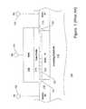
- FIGURE 1shows a cross-sectional view of an exemplary prior art SOI NMOSFET 100.
- the prior art SOI NMOSFET 100includes an insulating substrate 118 that may comprise a buried oxide layer, sapphire, or other insulating material.
- a source 112 and drain 116 of the NMOSFET 100comprise N+ regions ( i.e ., regions that are heavily doped with an "n-type” dopant material) produced by ion implantation into a silicon layer positioned above the insulating subtrate 118.
- the source and drain of PMOSFETscomprise P+ regions ( i.e ., regions heavily doped with "p-type” dopant material)).
- the body 114comprises a P- region (i.e ., a region that is lightly doped with a "p-type” dopant), produced by ion implantation, or by dopants already present in the silicon layer when it is formed on the insulating substrate 118.
- the NMOSFET 100also includes a gate oxide 110 positioned over the body 114.
- the gate oxide 110typically comprises a thin layer of an insulating dielectric material such as SiO 2 .
- the gate oxide 110electrically insulates the body 114 from a gate 108 positioned over the gate oxide 110.
- the gate 108comprises a layer of metal or, more typically, polysilicon.
- a source terminal 102is operatively coupled to the source 112 so that a source bias voltage "Vs" may be applied to the source 112.
- a drain terminal 106is operatively coupled to the drain 116 so that a drain bias voltage "Vd” may be applied to the drain 116.
- a gate terminal 104is operatively coupled to the gate 108 so that a gate bias voltage "Vg" may be applied to the gate 108.
- a positive gate biascreates a channel in the channel region of the MOSFET body through which current passes between the source and drain.
- a depletion mode devicea channel is present for a zero gate bias. Varying the voltage applied to the gate modulates the conductivity of the channel and thereby controls the current flow between the source and drain.
- the gate biascreates a so-called “inversion channel” in a channel region of the body 114 under the gate oxide 110.
- the inversion channelcomprises carriers having the same polarity (e.g ., "P" polarity (i.e ., hole carriers), or "N" polarity ( i.e ., electron carriers) carriers) as the polarity of the source and drain carriers, and it thereby provides a conduit ( i.e ., channel) through which current passes between the source and the drain.
- Ppolarity
- Npolarity
- conduiti.e ., channel
- an inversion channelis formed in the channel region of the body 114.
- the polarity of carriers in the inversion channelis identical to the polarity of carriers in the source and drain.
- the carriers in the channelcomprise N polarity carriers.
- the carriers in the channel of turned on (i.e ., conducting) PMOSFETscomprise P polarity carriers.
- Depletion mode MOSFETsoperate similarly to enhancement mode MOSFETs, however, depletion mode MOSFETs are doped so that a conducting channel exists even without a voltage being applied to the gate. When a voltage of appropriate polarity is applied to the gate the channel is depleted. This, in turn, reduces the current flow through the depletion mode device.
- the depletion mode deviceis analogous to a "normally closed” switch, while the enhancement mode device is analogous to a "normally open” switch.
- Both enhancement and depletion mode MOSFETshave a gate voltage threshold, V th , at which the MOSFET changes from an off-state (non-conducting) to an on-state (conducting).
- accumulated chargeis used herein to refer to gate-bias induced carriers that may accumulate in the body of an off-state MOSFET, even if the majority carriers in the body do not have the same polarity as the accumulated charge. This situation may occur, for example, in an off-state depletion mode NMOSFET, wherein the accumulated charge may comprise holes ( i.e ., having P polarity) even though the body doping is N- rather than P-.
- an accumulated charge 120may accumulate in the body 114 underneath and proximate the gate oxide 110.
- the operating state of the SOI NMOSFET 100 shown in FIGURE 1is referred to herein as an "accumulated charge regime" of the MOSFET.
- the accumulated charge regimeis defined in more detail below. The causes and effects of the accumulated charge in SOI MOSFETs are now described in more detail.
- electron-hole pair carriersmay be generated in MOSFET bodies as a result of several mechanisms (e.g ., thermal, optical, and band-to-band tunneling electron-hole pair generation processes).
- electron-hole pair carriersWhen electron-hole pair carriers are generated within an NMOSFET body, for example, and when the NMOSFET is biased in an off-state condition, electrons may be separated from their hole counterparts and pulled into both the source and drain. Over a period of time, assuming the NMOSFET continues to be biased in the off-state, the holes (resulting from the separated electron-hole pairs) may accumulate under the gate oxide (i.e ., forming an "accumulated charge") underneath and proximate the gate oxide.
- a similar process(with the behavior of electrons and holes reversed) occurs in similarly biased PMOSFET devices. This phenomenon is now described with reference to the SOI NMOSFET 100 of FIGURE 1 .
- the accumulated chargeis opposite in polarity to the polarity of carriers in the channel. Because, as described above, the polarity of carriers in the channel is identical to the polarity of carriers in the source and drain, the polarity of the accumulated charge 120 is also opposite to the polarity of carriers in the source and drain. For example, under the operating conditions described above, holes (having "P" polarity) accumulate in off-state NMOSFETs, and electrons (having "N” polarity) accumulate in off-state PMOSFETs. Therefore, a MOSFET device is defined herein as operating within the "accumulated charge regime" when the MOSFET is biased to operate in an off-state, and when carriers having opposite polarity to the channel carriers are present in the channel region.
- a MOSFETis defined as operating within the accumulated charge regime when the MOSFET is biased to operate in an off-state, and when carriers are present in the channel region having a polarity that is opposite the polarity of the source and drain carriers.
- the accumulated charge 120comprises hole carriers having P or "+" polarity.
- the carriers in the source, drain, and channeli.e ., when the FET is in the on-state
- the carriers in the source, drain, and channeli.e ., when the FET is in the on-state
- the SOI NMOSFET 100is therefore shown in FIGURE 1 as operating in the accumulated charge regime. It is biased to operate in an off-state, and an accumulated charge 120 is present in the channel region.
- the accumulated charge 120is opposite in polarity (P) to the polarity of the channel, source and drain carriers (N).
- V this negative by definition.
- the body 114comprises an N-region (as contrasted with the P- region shown in FIGURE 1 ).
- the source and draincomprise N+ regions similar to those shown in the enhancement mode MOSFET 100 of FIGURE 1 .
- Vs and Vdboth at zero volts, when a gate bias Vg is applied that is sufficiently negative relative to V th (for example, a Vg that is more negative than approximately -1 V relative to V th ), the depletion mode NMOSFET is biased into an off-state. If biased in the off-state for a sufficiently long period of time, holes may accumulate under the gate oxide and thereby comprise the accumulated charge 120 shown in FIGURE 1 .
- Vs and Vdmay comprise nonzero bias voltages.
- Vgmust be sufficiently negative to both Vs and Vd (in order for Vg to be sufficiently negative to V th , for example) in order to bias the NMOSFET in the off-state.
- bias voltagesmay be used to practice the present teachings. As described below in more detail, the present disclosed method and apparatus contemplates use in any SOI MOSFET device biased to operate in the accumulated charge regime.
- SOI and SOS MOSFETsare often used in applications in which operation within the accumulated charge regime adversely affects MOSFET performance. As described below in more detail, unless the accumulated charge is removed or otherwise controlled, it detrimentally affects performance of SOI MOSFETs under certain operating conditions.
- One exemplary application, described below in more detail with reference to the circuits shown in FIGURES 2B and 5Ais the use of SOI MOSFETs in the implementation of radio frequency (RF) switching circuits.
- RFradio frequency
- the inventorshave discovered that unless the accumulated charge is removed or otherwise controlled, under some operating conditions, the accumulated charge adversely affects the linearity of the SOI MOSFET and thereby increases harmonic distortion and intermodulation distortion (IMD) caused by the MOSFET when used in the implementation of certain circuits.
- IMDharmonic distortion and intermodulation distortion
- the inventorshave discovered that removal or control of the accumulated charge improves the drain-to-source breakdown voltage (i.e ., the "BVDSS") characteristics of the SOI MOSFETs.
- Apparatuses and methodsare provided to control accumulated charge in SOI MOSFETs, thereby improving nonlinear responses and harmonic and intermodulaton distortion effects in the operation of the SOI MOSFETs.
- a circuit having at least one SOI MOSFETis configured to operate in an accumulated charge regime.
- An accumulated charge sink (ACS)operatively coupled to the body of the SOI MOSFET, receives accumulated charge generated in the body, thereby reducing the nonlinearity of the net source-drain capacitance of the SOI MOSFET.
- the ACScomprises a high impedance connection to the MOSFET body, with an exemplary impedance greater than 10 6 ohm.
- FIGURE 1is a cross-sectional view of an exemplary prior art SOI NMOSFET.
- FIGURE 2Ais a simplified schematic of an electrical model showing the off-state impedance characteristics of the exemplary prior art SOI NMOSFET of FIGURE 1 .
- FIGURE 2Bis a schematic of an exemplary simplified RF switching circuit implemented using prior art SOI MOSFETs such as the prior art SOI NMOSFET of FIGURE 1 .
- FIGURES 3A and 3Bare simplified schematic diagrams of a top view of an improved SOI NMOSFET adapted to control accumulated charge in accordance with the present teachings.
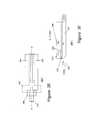
- FIGURE 3Cis a cross-sectional perspective schematic of an improved SOI NMOSFET adapted to control accumulated charge showing gate, source, drain and accumulated charge sink (ACS) terminals.
- ACSaccumulated charge sink
- FIGURE 3Dis a simplified top view schematic of an improved SOI NMOSFET adapted to control accumulated charge having an accumulated charge sink (ACS) electrically coupled to a P+ region.
- ACSaccumulated charge sink
- FIGURE 3Eis a simplified top view schematic of an improved SOI NMOSFET adapted to control accumulated charge and showing a cross-sectional view line A-A' taken along approximately a center of the SOI NMOSFET.
- FIGURE 3Fis a cross-sectional view of the improved SOI NMOSET of FIGURE 3E taken along the A-A' view line of FIGURE 3E .
- FIGURE 3Gis a cross-sectional view of the improved SOI NMOSET of FIGURES 3A-3B .
- FIGURE 3His a simplified top view schematic of an SOI NMOSFET illustrating a region of increased threshold voltage that can occur in prior art MOSFETs and in some embodiments of the improved SOI MOSFET due to manufacturing processes.
- FIGURE 3Iis a plot of inversion channel charge as a function of applied gate voltage when a region of increased threshold voltage is present in an SOI MOSFET.
- FIGURE 3Jis a simplified top view schematic of an improved SOI NMOSFET adapted to control accumulated charge and configured in a "T-gate" configuration.
- FIGURE 3Kis a simplified top view schematic of an improved SOI NMOSFET adapted to control accumulated charge and configured in an "H-gate" configuration.
- FIGURE 4Ais a simplified schematic of an improved SOI NMOSFET adapted to control accumulated charge embodied as a four terminal device.
- FIGURE 4Bis a simplified schematic of an improved SOI NMOSFET adapted to control accumulated charge, embodied as a four terminal device, wherein an accumulated charge sink (ACS) terminal is coupled to a gate terminal.
- ACSaccumulated charge sink
- FIGURE 4Cis a simplified schematic of an improved SOI NMOSFET adapted to control accumulated charge, embodied as a four terminal device, wherein an accumulated charge sink (ACS) terminal is coupled to a gate terminal via a diode.
- ACSaccumulated charge sink
- FIGURE 4Dis a simplified schematic of an improved SOI NMOSFET adapted to control accumulated charge, embodied as a four terminal device, wherein an accumulated charge sink (ACS) terminal is coupled to a control circuit.
- ACSaccumulated charge sink
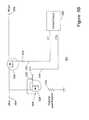
- FIGURE 4Eis a simplified schematic of an exemplary RF switch circuit implemented using the four terminal ACC NMOSFET of FIGURE 4D , wherein the ACS terminal is driven by an external bias source.
- FIGURE 4Fis a simplified schematic of an improved SOI NMOSFET adapted to control accumulated charge, embodied as a four terminal device, wherein an accumulated charge sink (ACS) terminal is coupled to a clamping circuit.
- ACSaccumulated charge sink
- FIGURE 4Gis a simplified schematic of an improved SOI NMOSFET adapted to control accumulated charge, embodied as a four terminal device, wherein an accumulated charge sink (ACS) terminal is coupled to a gate terminal via a diode in parallel with a capacitor.
- ACSaccumulated charge sink
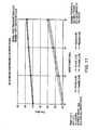
- FIGURE 4Hshows plots of the off-state capacitance (C off ) versus applied drain-to-source voltages for SOI MOSFETs operated in the accumulated charge regime, wherein a first plot shows the off-state capacitance C off of a prior art SOI MOSFET, and wherein a second plot shows the off-state capacitance C off of the improved ACC SOI MOSFET made in accordance with the present teachings.
- FIGURE 5Ais a schematic of an exemplary prior art single pole, single throw (SPST) radio frequency (RF) switch circuit.
- SPSTsingle pole, single throw
- RFradio frequency
- FIGURE 5Bis a schematic of an RF switch circuit adapted for improved performance using accumulated charge control, wherein the gate of a shunting SOI NMOSFET is coupled to an accumulated charge sink (ACS) terminal.
- ACSaccumulated charge sink
- FIGURE 5Cis a schematic of an RF switch circuit adapted for improved performance using accumulated charge control, wherein the gate of a shunting SOI NMOSFET is coupled to an accumulated charge sink (ACS) terminal via a diode.
- ACSaccumulated charge sink
- FIGURE 5Dis a schematic of an RF switch circuit adapted for improved performance using accumulated charge control, wherein the accumulated charge sink (ACS) terminal is coupled to a control circuit.
- ACSaccumulated charge sink
- FIGURE 6is a schematic of an RF switch circuit including stacked MOSFETs, adapted for improved performance using accumulated charge control, wherein the accumulated charge sink (ACS) terminals of the shunting stacked MOSFETs are coupled to a control signal.
- ACSaccumulated charge sink
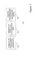
- FIGURE 7shows a flowchart of an exemplary method of improving the linearity of an SOI MOSFET device using an accumulated charge sink in accordance with the present disclosure.
- FIGURE 8shows a simplified circuit schematic of an exemplary embodiment of an RF switch circuit made in accordance with the present disclosure, wherein the RF switch circuit includes drain-to-source resistors between the drain and source of the ACC MOSFETs.
- FIGURE 9shows a simplified schematic of an exemplary single-pole double-throw (SPDT) RF switch circuit made in accordance with the present disclosure, wherein drain-to-source resistors are shown across the switching ACC SOI MOSFETs.
- SPDTsingle-pole double-throw
- FIGURES 10-19show exemplary performance results obtainable using the disclosed methods and apparatus for an exemplary single pole, six throw (SP6T) RF switch.
- SP6Tsingle pole, six throw
- the MOSFETAs described above in the background, no matter what mode of operation the MOSFET employs (i.e ., enhancement mode or depletion mode), under some circumstances, when a MOSFET is operated in an off-state with a nonzero gate bias voltage applied with respect to the source and drain, an accumulated charge may occur under the gate. According to the present teachings, as described above when the MOSFET is in an off-state, and when carriers are present in the channel region having a polarity that is opposite the polarity of the source and drain carriers, the MOSFET is defined herein as operating in the accumulated charge regime.
- the inventorshave observed that, when used in certain circuit implementations, MOSFETs operating in the accumulated charge regime exhibit undesirable non-linear characteristics that adversely impact circuit performance.
- the accumulated charge 120( FIGURE 1 ) adversely affects the linearity of off-state SOI MOSFETs, and more specifically, it adversely affects the linearity of contributing capacitances to the drain-to-source capacitance (Cds).
- Cdsis referred to as C off .
- FIGURE 2Ais a simplified schematic of an electrical model 200 showing the off-state impedance (or conversely, conductance) characteristics of the exemplary prior art SOI NMOSFET 100 of FIGURE 1 . More specifically, the model 200 shows the impedance characteristics from the source 112 to the drain 116 when the NMOSFET 100 is operated in the off-state. Because the drain-to-source off-state impedance characteristic of the NMOSFET 100 is primarily capacitive in nature, it is referred to herein as the drain-to-source off-state capacitance (C off ).
- C offdrain-to-source off-state capacitance
- the gate 108is understood to be biased at a voltage Vg by a circuit (not shown) that has an impedance that is large compared to the impedances of the contributing capacitances described in reference to FIGURE 2A .
- a circuitnot shown
- this exemplary descriptionmay be modified for the case wherein the impedance of the circuit providing the Vg bias is not large compared to the impedances of the contributing capacitances.
- the junction between the source 112 and the body 114 (i.e., a source-body junction 218) of the off-state NMOSFET 100can be represented by a junction diode 208 and a junction capacitor 214, configured as shown.
- the junction between the drain 116 and the body 114 (i.e., the drain-body junction 220) of the off-state NMOSFET 100can be represented by a junction diode 210 and a junction capacitor 216, configured as shown.
- the body 114is represented simply as an impedance 212 that is present between the source-body junction 218 8 and the drain-body junction 220.
- a capacitor 206represents the capacitance between the gate 108 and the body 114.
- a capacitor 202represents the capacitance between the source 112 and the gate 108, and another capacitor 204 represents the capacitance between the drain 116 and the gate 108.
- a substrate capacitance due to the electrical coupling between the source 112 and the drain 116 (through the insulating substrate 118 shown in FIGURE 1 )is taken to be negligibly small in the exemplary description set forth below, and therefore is not shown in the electrical model 200 of FIGURE 2A .
- the body 114is depleted of charge carriers.
- the body impedance 212is analogous to the impedance of an insulator, and the electrical conductance through the body 114 is very small (i.e ., the NMOSFET 100 is in the off-state). Consequently, the principal contributions to the drain-to-source off-state capacitance C off are provided by the capacitors 202 and 204.
- the capacitors 202 and 204are only slightly voltage dependent, and therefore do not significantly contribute to a nonlinear response that adversely affects harmonic generation and intermodulation distortion characteristics.
- the NMOSFET 100operates within the accumulated charge regime, and the accumulated charge 120 is therefore present in the body 114, mobile holes comprising the accumulated charge produce p-type conductivity between the source-body junction 218 and the drain-body junction 220.
- the accumulated charge 120produces an impedance between the source-body junction 218 and the drain-body junction 220 that is significantly less than the impedance between the junctions in the absence of the accumulated charge. If a Vds voltage is applied between the drain 116 and the source 112, the mobile holes redistribute according to the electrical potentials that result within the body 114.
- DC and low-frequency current flow through the SOI NMOSFET 100is prevented by the diode properties of the source-body junction 218 and the drain-body junction 220, as represented by the junction diodes 208 and 210, respectively. That is, because the junction diodes 208 and 210 are anti-series ( i.e ., "back-to-back") in this case, no DC or low-frequency currents flow through the SOI NMOSFET 100. However, high-frequency currents may flow through the SOI NMOSFET 100 via the capacitances of the source-body junction 218 and the drain-body junction 220, as represented by the junction capacitors 214 and 216, respectively.
- the junction capacitors 214 and 216are voltage dependent because they are associated with junctions between n-type and p-type regions. This voltage dependence results from the voltage dependence of the width of the depletion region of the junction between the n-type and p-type regions. As a bias voltage is applied to the NMOSFET, the width of the depletion region of the junction between the n-type and p-type regions is varied. Because the capacitance of the junction depends on the width of the junction depletion region, the capacitance also varies as a function of the bias applied across the junction ( i.e ., the capacitance is also voltage dependent).
- capacitors 202 and 204may also have a voltage dependence caused by the presence of the accumulated charge 120. Although the complex reasons for this voltage dependence are not described in detail herein, persons skilled in the arts of electronic devices shall understand that electric field regions (e.g ., electric field regions 122 and 124 described above with reference to FIGURE 1 ) may be affected by the response of the accumulated charge and its response to an applied Vds, thereby causing a voltage dependence of capacitors 202 and 204. An additional nonlinear effect may occur due to a direct capacitance (not shown) between the source 112 and the drain 116.
- electric field regionse.g ., electric field regions 122 and 124 described above with reference to FIGURE 1
- An additional nonlinear effectmay occur due to a direct capacitance (not shown) between the source 112 and the drain 116.
- this direct capacitancewould usually be expected to be negligible for most SOI MOSFETs, it may contribute for SOI MOSFETs having very short spacing between the source and drain.
- the contribution of this direct capacitance to C offis also voltage-dependent in the presence of an accumulated charge, for reasons that are analogous to the voltage dependencies of the capacitors 202 and 204 as described above.
- IMDintermodulation distortion
- the relative contributions of these effectsare complex, and depend on fabrication processes, biases, signal amplitudes, and other variables.
- those skilled in the electronic device design artsshall understand from the teachings herein that reducing, removing, or otherwise controlling the accumulated charge provides an overall improvement in the nonlinear behavior of C off .
- the body impedance 212is significantly decreased in the presence of the accumulated charge 120, the magnitude of C off may be increased when the FET operates in the accumulated charge regime. Reducing, removing, or otherwise controlling the accumulated charge also mitigates this effect.
- the accumulated chargedoes not accumulate in the body in an instant as soon as the FET transitions from an on-state (conducting state) to an off-state (non-conducting state). Rather, when the FET transitions from the on-state to the off-state, it begins to accumulate charge in the body of the MOSFET, and the amount of accumulated charge increases over time. The accumulation of the accumulated charge therefore has an associated time constant (i.e ., it does not instantly reach a steady-state level of accumulated charge). The accumulated charge accumulates slowly in the FET body. The depleted FET has a C off associated with it which is increased with an increasing amount of accumulated charge.
- RF switch linearityis an important design parameter in many applications. Improved switch linearity leads to improved suppression of harmonic and intermodulation (IM) distortion of signals processed by the switch. These improved switch characteristics can be critically important in some applications such as use in cellular communication devices.
- the well known GSM cellular communication system standardimposes stringent linearity, harmonic and intermodulation suppression, and power consumption requirements on front-end components used to implement GSM cell phones.
- One exemplary GSM standardrequires that all harmonics of a fundamental signal be suppressed to below -30 dBm at frequencies up to 12.75 GHz. If harmonics are not suppressed below these levels, reliable cell phone operation can be significantly adversely impacted ( e.g ., increased dropped calls or other communication problems may result due to harmonic and intermodulation distortion of the transmit and receive signals).
- the RF switching functionis generally implemented in the cell phone front-end components, improvements in the RF switch linearity, harmonic and intermodulation suppression, and power consumption performance characteristics is highly desirable. A description of how the non-linear behavior of the off-state capacitance C off of the prior art MOSFETs adversely affects these RF switch characteristics is now described with reference to FIGURE 2B .
- FIGURE 2Billustrates an exemplary simplified RF switch circuit 250 implemented using prior art MOSFETs such as the prior art SOI NMOSFET 100 described above with reference to FIGURE 1 .
- MOSFETssuch as the prior art SOI NMOSFET 100 described above with reference to FIGURE 1 .
- FIGURE 2Bthe prior art RF switch 250 includes a single "pass” or “switching" MOSFET 254 operatively coupled to five shunting MOSFETs 260a-260e.
- the MOSFET 254acts as a pass or switching transistor and is configured, when enabled, to selectively couple an RF input signal (applied to its drain, for example) to an RF antenna 258 via a transmission path 256.
- the shunting MOSFETs, 260a-260ewhen enabled, act to alternatively shunt the RF input signal to ground.
- the switching MOSFET 254is selectively controlled by a first switch control signal (not shown) coupled to its gate, and the shunting MOSFETs, 260a-260e are similarly controlled by a second switch control signal (not shown) coupled to their gates.
- the switching MOSFET 254is thereby enabled when the shunting MOSFETs 260a-260e are disabled, and vice versa. As shown in the exemplary embodiment of the RF switch 250 of FIGURE 2B , the switching MOSFET 254 is enabled by applying a gate bias voltage of +2.5V (via the first switch control signal). The shunting MOSFETs 260a-260e are disabled by applying a gate bias voltage of -2.5V (via the second switch control signal).
- the RF signal 252propagates through the switching MOSFET 254, through the transmission path 256, and to the antenna 258.
- the shunting MOSFETS 260a-260ecomprise prior art SOI (or SOS) MOSFETs, such as the SOI NMOSFET 100 ( FIGURE 1 )
- an accumulated chargecan occur in the SOI MOSFET bodies ( i.e ., when the SOI MOSFETs operate in the accumulated charge regime as described above).
- the accumulated chargecan produce nonlinear behavior in the off-state capacitance C off of the SOI MOSFETs when AC voltages are applied to the MOSFETs.
- the RF signalapplies time varying source-to-drain bias voltages to the SOI MOSFETs 260a-260e.
- the time varying source-to-drain bias voltagescreates movement of the accumulated charge within the channel regions of the SOI MOSFETs 260-260e.
- the movement of the accumulated charge within the channel regions of the SOI MOSFETscauses variations in the drain-to-source off-state capacitance of the SOI MOSFETs 260a-260e.
- the movement of the accumulated charge within the channel regionscauses a voltage dependence of the drain-to-source off-state capacitance as described above with reference to FIGURE 2A .
- the voltage dependent variations in the off-state capacitance of the SOI MOSFETs 260a-260eis the dominant cause of harmonic distortion and IMD of the RF signal as it propagates through the RF switch 250.
- harmonic distortion and IMD of the RF signalis a major disadvantage of the prior art RF switch circuits implemented using the prior art SOI MOSFET devices.
- harmonics and IMD of the RF signalmust be suppressed to levels that heretofore have been difficult or impossible to achieve using prior art SOI MOSFET devices.
- prior art switchestypically have only a 6 dB margin to the GSM third order harmonics suppression requirement of less than -30 dBm.
- Very low even order harmonic distortionis also desirable in GSM systems as the second order harmonic of the GSM transmit band also resides in the DCS receive band. Suppression of odd order (e.g ., third order) harmonics of the RF signal, however, is desirable and improvements in that regard are needed.
- BVDSSdrain-to-source breakdown voltage
- the present disclosed method and apparatus for improving linearity of SOI (and SOS) MOSFET devicesovercomes the above-described disadvantages of the prior art.
- the accumulated chargeis recognized as a major source of harmonic distortion, IMD and compression/saturation in off-state SOI MOSFET devices, and in circuits (such as RF circuits) implemented with these devices, it becomes clear that reduction, removal, and/or control of the accumulated charge improves the harmonic suppression characteristics of these devices.
- reduction, removal, and/or control of the accumulated chargealso improve the BVDSS performance characteristics by preventing the parasitic bipolar action from occurring. Improvements in BVDSS lead to consequent improvements in device linearity.
- Several exemplary structures and techniques for controlling the accumulated charge in SOI MOSFETsare described in detail in the next section.
- the present disclosuredescribes methods and apparatuses for improving semiconductor device linearity (e.g ., reducing adverse harmonic distortion and IMD effects) in SOI MOSFETs.
- the method and apparatusimproves the linearity and controls the harmonic distortion and IMD effects of the MOSFET devices by reducing the accumulated charge in the bodies of the MOSFET devices.
- the present method and apparatusreduces or otherwise controls the accumulated charge in the MOSFET bodies using an accumulated charge sink (ACS) that is operatively coupled to the MOSFET body.
- ACSaccumulated charge sink
- the present method and apparatusentirely removes all of the accumulated charge from the bodies of the MOSFET devices.
- the MOSFETis biased to operate in an accumulated charge regime
- the ACSis used to entirely remove, reduce, or otherwise control, the accumulated charge and thereby reduce harmonic distortions and IMD that would otherwise result.
- Linearityis also improved in some embodiments by removing or otherwise controlling the accumulated charge thereby improving the floating body MOSFET BVDSS characteristics.
- MOSFETsfabricated on Semiconductor-On-Insulator ("SOI") and Semiconductor-On-Sapphire (“SOS”) substrates.
- SOISemiconductor-On-Insulator
- SOSSemiconductor-On-Sapphire
- the present teachingscan be used in the implementation of MOSFETs using any convenient semiconductor-on-insulator technology.
- inventive MOSFETs described hereincan be implemented using compound semiconductors fabricated on insulating substrates, such as GaAs MOSFETs.
- the present method and apparatusmay also be applied to silicon-germanium (SiGe) SOI MOSFETs.
- the present disclosureis particularly applicable to FETs and associated applications benefiting from a fully depleted channel when the FET is operated in the off-state, wherein an accumulated charge may result.
- the disclosed method and apparatus for use in improving the linearity of MOSFETsalso finds applicability for use with partially depleted channels.
- the doping and dimensions of the bodyvary widely.
- the bodycomprises silicon having a thickness of approximately 100 angstroms to approximately 2,000 angstroms.
- dopant concentration within the FET bodiesranges from no more than that associated with intrinsic silicon to approximately 1 X 10 18 active dopant atoms per cm 3 , resulting in fully-depleted transistor operation.
- dopant concentration within the FET bodiesranges from 1 x 10 18 to 1 x 10 19 active dopant atoms per cm 3 and/or the silicon comprising the body ranges from a thickness of 2000 angstroms to many micrometers, resulting in partially-depleted transistor operation.
- the present disclosed method and apparatus for use in improving linearity of MOSFETscan be used in MOSFETs implemented in a wide variety of dopant concentrations and body dimensions. The present disclosed method and apparatus therefore is not limited for use in MOSFETs implemented using the exemplary dopant concentrations and body dimensions as set forth above.
- accumulated charge within a FET bodyis reduced using control methodologies and associated circuitry. In one embodiment all of the accumulated charge is removed from the FET body. In other embodiments, the accumulated charge is reduced or otherwise controlled. In one embodiment, holes are removed from the FET body, whereas in another embodiment, electrons are removed from the FET body, as described below in more detail. By removing holes (or electrons) from the FET body using the novel and nonobvious teachings of the present disclosure, voltage induced variations in the parasitic capacitances of the off-state FETs are reduced or eliminated, thereby reducing or eliminating nonlinear behavior of the off-state FETs.
- Accumulated charge controlnot only facilitates a beneficial overall reduction in the FET off-state capacitance C off (as described above with reference to FIGURE 2A and below with reference to FIGURE 4H ), it also facilitates a reduction in C off variations that can occur over time in the presence of a time varying V ds bias voltage.
- a reduction of undesirable harmonics generation and intermodulation distortion in RF switch circuitsis obtained using SOI MOSFETs made in accordance with the present disclosure.
- Improved SOI MOSFET power handling, linearity, and performanceare achieved by devices made in accordance with the present teachings. While the methods and apparatuses of the present disclosure are capable of fully removing accumulated charge from the FET bodies, those skilled in the electronic device design arts shall appreciate that any reduction of accumulated charge is beneficial.
- SOI systemsinclude any semiconductor architecture employing semiconductor-containing regions positioned above an underlying insulating substrate. While any suitable insulating substrate can be used in a SOI system, exemplary insulating substrates include silicon dioxide (e.g ., a buried oxide layer supported by a silicon substrate, such as that known as Separation by Implantation of Oxygen (SIMOX)), bonded wafer (thick oxide), glass, and sapphire. As noted above, in addition to the commonly used silicon-based systems, some embodiments of the present disclosure may be implemented using silicon-germanium (SiGe), wherein the SiGe is used equivalently in place of Si.
- SiGesilicon-germanium
- an ACSis used to remove or otherwise control accumulated charge (referenced as 120 in FIGURE 1 described above) from the MOSFETs when the MOSFETs are configured to operate in the accumulated charge regime.
- SOIor SOS
- ACCAccumulated Charge Control
- the ACC MOSFETsare useful in improving performance of many circuits, including RF switching circuits.
- FIGURES 3A-3KVarious characteristics and possible configurations of the exemplary ACC MOSFETs are described in detail below with reference to FIGURES 3A-3K . This section also describes how the exemplary ACS implementations of the present disclosure differ from the body contacts of the prior art.
- FIGURE 4AThe ACC MOSFET is shown schematically embodied as a four-terminal device in FIGURE 4A .
- FIGURES 4B-4Gshow various exemplary simple circuit configurations that can be used in removing the accumulated charge from the ACC MOSFET when it operates in an accumulated charge regime. The operation of the simplified circuit configurations is described in more detail below with reference to FIGURES 4A-4G .
- the improvement in off-state capacitance C off of the ACC MOSFETs, as compared with the off-state capacitance of the prior art SOI MOSFETs,is described below with reference to FIGURE 4H .
- FIGURES 5B-5DThe operation of various exemplary RF switch circuits implemented using the ACC MOSFETs of the present disclosure is described below with reference to the circuit schematics of FIGURES 5B-5D . Further, an exemplary RF switch circuit using stacked ACC MOSFETs (for increased power handling) of the present disclosure is described below with reference to FIGURE 6 . An exemplary method of improving the linearity of an SOI MOSFET using an accumulated charge sink (ACS) is described with reference to FIGURE 7 . Finally, exemplary fabrication methods that may be used to manufacture the ACC MOSFET are described. The various exemplary ACS implementations and structures that can be used to practice the disclosed method and apparatus are now described with reference to FIGURES 3A-3K .
- FIGURES 3A and 3Bare simplified schematic diagrams of a top view of an Accumulated Charge Control (ACC) SOI NMOSFET 300 adapted to control accumulated charge 120 ( FIGURE 1 ) in accordance with the present disclosure.
- a gate contact 301is coupled to a first end of a gate 302.
- a gate oxide (not shown in FIGURE 3A but shown in FIGURE 1 ) and a body 312 (shown in FIGURE 3B )are positioned under the gate 302.
- a source 304 and a drain 306comprise N+ regions.
- the ACC NMOSFET 300includes an accumulated charge sink (ACS) 308 comprising a P- region.
- ACSaccumulated charge sink
- the ACS 308is coupled to and is in electrical communication with the body 312 which also comprises a P- region.
- An electrical contact region 310provides electrical connection to the ACS 308.
- the electrical contact region 310comprises a P+ region. As shown in FIGURE 3A , the electrical contact region 310 is coupled to and is in electrical communication with the ACS 308.
- the electrical contact region 310may be used to facilitate electrical coupling to the ACS 308 because in some embodiments it may be difficult to make a direct contact to a lightly doped region.
- the ACS 308 and the electrical contact region 310may be coextensive.
- the electrical contact region 310comprises an N+ region.
- the electrical contact region 310functions as a diode connection to the ACS 308, which prevents positive current flow into the ACS 308 (and also prevents positive current flow into the body 312) under particular bias conditions, as described below in more detail.
- FIGURE 3Bis an alternative top view of the ACC SOI NMOSFET 300 of FIGURE 3A , illustrating the ACC NMOSFET 300 without its gate contact 301, gate 302, and gate oxide being visible. This view allows the body 312 to be visible.
- FIGURE 3Bshows the coupling of the ACS 308 to one end of the body 312.
- the body 312 and the ACS 308comprise a combined P- region that may be produced by a single ion-implantation step.
- the body 312 and ACS 308comprise separate P- regions that are coupled together.
- the ACC NMOSFET 300 of FIGURES 3A and 3Bcan be implemented as an ACC PMOSFET simply by reversing the dopant materials used to implement the various FET component regions (i.e ., replace p-type dopant material with n-type dopant material, and vice versa ).
- the source and draincomprise P+ regions
- the bodycomprises an N- region.
- the ACS 308also comprises an N- region.
- the electrical contact region 310may comprise an N+ region.
- the region 310comprises a P+ region, which functions as a diode connection to the ACS 308 and thereby prevents current flow into the ACS 308 under particular bias conditions.
- the ACS 308 used to implement ACC SOI MOSFETsincludes novel features in structure, function, operation and design that distinguish it from the so-called “body contacts” (also sometimes referred to as “body ties”, usually when the "body contact” is directly connected to the source) that are well known in the prior art.
- Exemplary references relating to body contacts used in prior art SOI MOSFETsinclude the following: (I) F. Hameau and O. Rozeau, Radio-Frequency Circuits Integration Using CMOS SOI 0.25 ⁇ m Technology," 2002 RF IC Design Workshop Europe, 19 - 22 March 2002, Grenoble, France ; (2) J. R. Cricci et al., "Silicon on Sapphire MOS Transistor," U. S. Patent No. 4,053,916, October 11, 1977 ; (3) O. Rozeau et al., "SOI Technologies Overview for Low-Power Low-Voltage Radio-Frequency Applications,” Analog Integrated Circuits and Signal Processing, 25, pp. 93-114, Boston, MA, Kluwer Academic Publishers, Nov.
- applicationssuch as RF switch circuits, may use SOI MOSFETs operated with off-state bias voltages, for which accumulated charge may result.
- the SOI MOSFETsare defined herein as operating within the accumulated charge regime when the MOSFETs are biased in the off-state, and when carriers having opposite polarity to the channel carriers are present in the channel regions of the MOSFETs.
- the SOI MOSFETsmay operate within the accumulated charge regime when the MOSFETs are partially depleted yet still biased to operate in the off-state.
- Significant benefits in improving nonlinear effects on source-drain capacitancecan be realized by removing or otherwise controlling the accumulated charge according to the present teachings.
- the ACS 308operates effectively to remove or otherwise control the accumulated charge from the SOI NMOSFET 300 using a high impedance connection to and throughout the body 312.
- High impedance ACSsmay be used because the accumulated charge 120 is primarily generated by phenomena (e.g ., thermal generation) that take a relatively long period of time to produce significant accumulated charge.
- a typical time period for producing non-negligible accumulated charge when the NMOSFET operates in the accumulated charge regimeis approximately a few milliseconds or greater.
- Such relatively slow generation of accumulated chargecorresponds to very low currents, typically less than 100 nA/mm of transistor width. Such low currents can be effectively conveyed even using very high impedance connections to the body.
- the ACS 308is implemented with a connection having a resistance of greater than 10 6 ohms. Consequently, the ACS 308 is capable of effectively removing or otherwise controlling the accumulated charge 120 even when implemented with a relatively high impedance connection, relative to the low impedance prior art body contacts.
- the relative rates for electron-hole pair generation by impact ionization versus the pair generation processes causing accumulated chargecan be estimated from the roll-off frequencies for the two phenomena.
- reference (3) cited aboveindicates roll-off frequencies for impact ionization effects in the range of 10 5 Hz.
- a roll-off frequency for the accumulated charge effectshas been observed to be in the range of 10 3 Hz or less, as indicated by recovery times for odd harmonics.
- impact ionizationprimarily occurs when the SOI MOSFET operates in an on-state
- the effects of impact ionizationcan be amplified by on-state transistor operation.
- Low impedance body contacts to and throughout a body regionis even more critical in these environments in order to control the effects of impact ionization under the on-state conditions.
- the ACS 308 of the present teachingsremoves or otherwise controls the accumulated charge only when the ACC SOI MOSFET operates in the accumulated charge regime.
- the FETis in the off-state in this regime, so there is no requirement to remove impact ionization as amplified by an on-state FET. Therefore, a high impedance ACS 308 is perfectly adequate for removing the accumulated charge under these operating conditions.
- the prior art requirements for low impedance body connectionsresults in numerous problems of implementation that are overcome by the present teachings, as described below in more detail.
- the ACS 308may be implemented with much lower source-to-drain parasitic capacitance as compared to the body contacts of the prior art.
- the above-described low impedance connection to the SOI MOSFET body required of the prior art body contactsnecessitates proximity of the contacts to the entire body. This may require a plurality body contact "fingers" that contact the body at different locations along the body.
- the low impedance connection to the bodyalso necessitates proximity of the prior art body contacts to the source and drain. Because of parasitic capacitances produced by such body contacts, the cited prior art references teach away from the use of such structures for many high frequency applications such as RF.
- the ACS 308 of the present disclosuremay be positioned a selected distance away from the source 304 and the drain 306, and the ACS 308 may also be coupled to the body 312 at a first distal end of the body 312 (shown in FIGURES 3A and 3B ). Arranged in this manner, the ACS 308 makes minimal contact (as compared to the prior art body contacts that may contact the body at many locations along the body) with the body 312. This configuration of the ACS 308 with the MOSFET eliminates or greatly reduces the parasitic capacitances caused by a more proximate positioning of the ACS 308 relative to the source, drain, and body. Further, the ACS 308 may be implemented in SOI MOSFETs operated with a depleted channel. In general, the cited prior art references teach away from the use of body contacts for this environment (see, e.g., reference (3), cited above).
- the prior artdoes not teach how to effectively implement very large body widths (i.e., much greater than approximately 10 ⁇ m).
- the ACS 308 of the present disclosed devicemay be implemented in SOI MOSFETs having relatively large body widths. This provides improvements in on-state conductance and transconductance, insertion loss and fabrication costs, particularly for RF switch devices. According to the prior art teachings cited above, larger body widths adversely affect the efficient operation of body contacts because their impedances are necessarily thereby increased.
- a plurality of fingersmay be used to contact the body at different locations, the plurality of fingers adversely affects parasitic source-to-drain capacitances, as described above.
- the present disclosureprovides novel MOSFET devices, circuits and methods that overcome the limitations according to the prior art teachings as cited above.
- FIGURE 3Cis a cross-sectional perspective schematic of an ACC SOI NMOSFET 300' adapted to control accumulated charge in accordance with the disclosed method and apparatus.
- the ACC NMOSFET 300'includes four terminals that provide electrical connection to the various FET component regions.
- the terminalsprovide means for connecting external integrated circuit (IC) elements (such as metal leads, not shown) to the various FET component regions.
- ICintegrated circuit
- Three of the terminals shown in FIGURE 3Care typically available in prior art FET devices.
- the ACC NMOSFET 300'includes a gate terminal 302' that provides electrical connection to the gate 302.
- the ACC NMOSFET 300'includes source and drain terminals 304', 306' that provide electrical connection to the source 304 and drain 306, respectively.
- the terminalsare coupled to their respective FET component regions (i.e ., gate, drain and source) via so-called "ohmic" (i.e ., low resistance) contact regions.
- "ohmic"i.e ., low resistance
- the ACC NMOSFET 300'is adapted to control accumulated charge when the NMOSFET operates in the accumulated charge regime.
- the ACC NMOSFET 300'includes a fourth terminal that provides electrical connection to the body 312, and thereby facilitates reduction (or other control) of the accumulated charge when the FET 300' operates in the accumulated charge regime. More specifically, and referring again to FIGURE 3C , the ACC NMOSFET includes a "body" terminal, or Accumulated Charge Sink (ACS) terminal 308'.
- ACSAccumulated Charge Sink
- the ACS terminal 308'provides an electrical connection to the ACS 308 (not shown in FIGURE 3C , but shown in FIGURES 3A and 3B ) and to the body 312.
- the ACS terminal 308'is shown in FIGURE 3C as being physically coupled to the body 312, those skilled in the electronic design arts shall understand that this depiction is for illustrative purposes only.
- the direct coupling of the ACS terminal 308' to the body 312 shown in FIGURE 3Cillustrates the electrical connectivity (i.e ., not the physical coupling) of the terminal 308' with the body 312.
- the other terminalsi.e ., terminals 302', 304' and 306'
- FIGURE 3Care also shown in FIGURE 3C as being physically coupled to their respective FET component regions.
- the ACS terminal 308'provides the electrical connection to the body 312 via coupling to the ACS 308 via the electrical contact region 310.
- the present disclosurealso contemplates embodiments where the coupling of the ACS terminal 308' is made directly to the body 312 ( i.e ., no intermediate regions exist between the ACS terminal 308' and the body 312).
- the ACC NMOSFET 300'when the ACC NMOSFET 300' is biased to operate in the accumulated charge regime (i.e ., when the ACC NMOSFET 300' is in the off-state, and there is an accumulated charge 120 of P polarity (i.e., holes) present in the channel region of the body 312), the accumulated charge is removed or otherwise controlled via the ACS terminal 308'.
- the charge 312can be removed or otherwise controlled by applying a bias voltage (V b (for "body”) or V ACS (ACS bias voltage)) to the ACS terminal 308'.
- the ACS bias voltage V ACS applied to the ACS terminal 308'may be selected to be equal to or more negative than the lesser of the source bias voltage Vs and drain bias voltage Vd. More specifically, in some embodiments, the ACS terminal 308' can be coupled to various accumulated charge sinking mechanisms that remove (or "sink") the accumulated charge when the FET operates in the accumulated charge regime. Several exemplary accumulated charge sinking mechanisms and circuit configurations are described below with reference to FIGURES 4A-5D .
- the ACC SOI NMOSFET 300' of FIGURE 3Ccan be biased to operate in the accumulated charge regime by applying specific bias voltages to the various terminals 302', 304', and 306'.
- the source and drain bias voltages(Vs and Vd, respectively) are zero ( i.e ., the terminals 304' and 306' are connected to ground).
- the ACC NMOSFET 300'operates in the off-state. If the ACC NMOSFET 300' continues to be biased in the off-state, the accumulated charge (holes) will accumulate in the body 312.
- the accumulated chargecan be removed from the body 312 via the ACS terminal 308'.
- the ACS terminal 308'is coupled to the gate terminal 302' (thereby ensuring that the same bias voltages are applied to both the gate (Vg) and the body (shown in FIGURE 3C as “Vb” or "V ACS ").
- bias voltagescan be applied to the four device terminals while still employing the techniques of the present disclosed method and apparatus.
- the ACC SOI NMOSFET 300'is biased to operate in the accumulated charge regime, the accumulated charge can be removed or otherwise controlled by applying a bias voltage V ACS to the ACS terminal 308', and thereby remove the accumulated charge from the body 312.
- V this negative by definition.
- both the Vs and Vd bias voltagescomprise zero volts (i.e ., both terminals tied to circuit ground node)
- a gate bias Vg applied to the gate terminal 302'is sufficiently negative to V th (for example, Vg is more negative than approximately -1V relative to V th )
- holesmay accumulate under the gate oxide 110 thereby becoming the accumulated charge 120.
- the voltage V ACS applied to the ACS 308may be selected to be equal to or more negative than the lesser of Vs and Vd.
- the source and drain bias voltages, Vs and Vdmay comprise voltage other than zero volts.
- the gate bias voltage Vgmust be sufficiently negative to both Vs and Vd (in order for Vg to be sufficiently negative to V th , for example) in order to bias the NMOSFET in the off-state.
- the ACS bias voltage V ACS applied to the ACS terminal 308'may be selected to be equal to or more negative than the lesser of Vs and Vd.
- V ACSshould, in the exemplary embodiments, be equal to or more negative than the lesser of Vs and Vd.
- Vs, Vd, Vg and V ACS bias voltagesmay be used when the ACC MOSFET comprises a PMOSFET device. Because the prior art body contacts are typically tied to the source, this implementation cannot be effected using the prior art body contact approach.
- FIGURE 3Dis a simplified schematic diagram of a top view of an ACC SOI NMOSFET 300" adapted to control accumulated charge 120 ( FIGURE 1 ) in accordance with the present disclosure.
- FIGURE 3Dshows the ACC NMOSFET 300" without its gate contact 301, gate 302, and gate oxide being visible.
- the ACC NMOSFET 300" of FIGURE 3Dis very similar in design to the ACC NMOSFET 300 described above with reference to FIGURES 3A and 3B .
- the ACC NMOSFET 300"includes a source 304 and drain 306 comprising N+ regions.
- the ACC NMOSFET 300"also includes an accumulated charge sink (ACS) 308 comprising a P- region.
- ACSaccumulated charge sink
- the P- region that comprises the ACS 308abuts ( i.e., is directly adjacent) the body 312, which also comprises a P- region.
- the ACC NMOSFET 300"includes an electrical contact region 310 that provides electrical connection to the ACS 308.
- the electrical contact region 310comprises a P+ region.
- the electrical contact region 310may comprise an N+ region (which thereby prevents positive current flow into the body 312 as noted above).
- the electrical contact region 310is formed in the ACC NMOSFET 300" directly adjacent the ACS 308.
- the ACC SOI NMOSFET 300"functions to control accumulated charge similarly to the operation of the ACC NMOSFETs described above with reference to FIGURES 3A-3C .
- FIGURE 3Eis a simplified schematic diagram of a top view of an ACC SOI NMOSFET 300"' adapted to control accumulated charge in accordance with the present disclosure.
- the ACC NMOSFET 300"'is very similar in design and function to the ACC NMOSFETs described above with reference to FIGURES 3A-3D .
- FIGURE 3Eshows a dashed cross-sectional view line A-A' taken along the approximate center of the NMOSFET 300"'. This cross-sectional view is used herein to describe structural and performance characteristics of some exemplary prior art MOSFETS and some embodiments of the ACC NMOSFET that may occur as a result of the fabrication processes. Details of this cross-sectional view A-A' are now described with reference to FIGURE 3F .
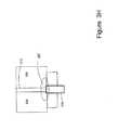
- View line A-A'slices through the following component regions of the ACC NMOSFET 300"': the P+ electrical contact region 310, the ACS 308 (shown in FIGURE 3E , but not shown in FIGURE 3F ), a P+ overlap region 310', a gate oxide 110, and a poly-silicon gate 302.
- the region 310is doped with p-type dopant material, proximate the P- body region, some additional P+ doping may be implanted ( i.e ., the p-type dopant material may overlap) into the P+ overlap region 310' of the poly-silicon gate 302.
- such overlappingis performed intentionally to ensure that all of the gate oxide 110 is completely covered by the P+ region (i.e ., to ensure that no gap exists on the edge of the oxide 110 between the gate 302 and the P+ region 310). This, in turn, aids in providing a minimum impedance connection between the P+ region 310 and the body 312.
- the present teachingsencompass such embodiments described above, those skilled in the electronic device design and manufacturing arts shall recognize that such low-resistance connections are not required. Therefore, disadvantages associated with the embodiment shown in FIGURE 3H , as described below in more detail, can be overcome by using other embodiments described herein (for example, the embodiments 300 and 300"" described below with reference to FIGURES 3G and 3J , respectively), in which gaps are intentionally implemented between the P+ region 310 and the body 312.
- the P+ overlap region 310'overlaps the oxide 110 by approximately 0.2 - 0.7 microns.
- the remaining area over the gate oxide 110 and over the P- bodyis doped with n-type dopant material (i.e ., it comprises an N+ region).
- an increased threshold voltage regionis created in the NMOSFET 300"'. More specifically, due to the P+ doping (in the P+ overlap region 310') proximate the edge 340 of the gate 302 over the channel region of the body 312, a region of increased threshold voltage is formed in that region of the MOSFET 300"'. The effects of the region of increased threshold voltage are now described in more detail with reference to FIGURES 3H and 3I .
- FIGURE 3Ishows a plot 380 of inversion channel charge versus applied gate voltage for an ACC NMOSFET.
- the plot 380 shown in FIGURE 3Iillustrates one effect of the above-described increased threshold voltage that can occur in prior art MOSFETs, and in some embodiments of the present ACC NMOSFETs due to certain manufacturing processes.
- the increased threshold voltage regionshown in FIGURE 3H and described in more detail below, also occurs in prior art MOSFET designs due to the proximity of body ties to the FET body.
- the present disclosed method and apparatuscan be used to reduce or eliminate the region of increased threshold voltage found in some prior art SOI MOSFET designs.
- FIGURE 3Hshows one embodiment of an ACC NMOSFET without its gate contact, gate, and gate oxide being visible.
- the MOSFET region of increased threshold voltage described above with reference to FIGURES 3E and 3Fis shown in FIGURE 3H as occurring in the region encompassed by the ellipse 307.
- the region 307 of the ACC MOSFET shown in FIGURE 3Heffectively "turns on” after the rest of the ACC MOSFET channel region.
- the increased threshold voltagecan be reduced by reducing the size of the region 307. Eliminating the region 307 altogether eliminates the threshold voltage increase. Because the threshold voltage increase can increase harmonic and intermodulation distortion of the "on" state MOSFET, eliminating this effect improves MOSFET performance. The increased threshold voltage also has the detrimental effect of increasing the MOSFET on-resistance (i.e ., the resistance presented by the MOSFET when it is in the on-state (conducting state), which detrimentally impacts the MOSFET insertion loss.
- the detrimental effects associated with threshold voltage increaseare mitigated or overcome by positioning the P+ region 310 a selected distance away from an edge of the poly-silicon gate 302. This approach is shown both in the top view of the ACC MOSFET 300 of FIGURE 3A , and in the cross-sectional view of the ACC MOSFET 300 shown in FIGURE 3G .
- the P+ region 310does not extend all the way to the edge 340 of the poly-silicon gate 302. This is in stark contrast to the embodiment 300"' shown in FIGURE 3F , where the P+ region 310' extends all the way to the gate edge 340.
- the P+ region 310By positioning the P+ region 310 a distance away from the gate edge 340 as shown in the embodiment 300 of FIGURE 3G , no P+ region is positioned proximate the poly-silicon gate 302 ( i.e ., there is no P+ region present in the poly-silicon gate 302).
- This configuration of the P+ region 310eliminates or greatly reduces the problems associated with threshold voltage increase as described above.
- the relatively high impedance of the ACS 308 P- region (shown in FIGURE 3A ) between the P+ region 310 and the gate 302does not adversely affect the performance of the ACC NMOSFET 300.
- the accumulated chargecan be effectively removed even using a relatively high impedance ACS connection.
- the threshold voltage increaseis removed by positioning the P+ region 310 (and the ACS 308) a distance away from the body 312. Because the electrical connectivity between the ACS 308 and the body 312 has relatively high impedance when the small region of P+ 310 is positioned a distance away from the body 312, this approach is never taught or suggested by the body contact prior art references (which require low impedance contacts as described above). This improved embodiment is described next with reference to FIGURE 3J .
- FIGURE 3Jis a simplified top view schematic of another embodiment of an ACC SOI NMOSFET 300"" adapted to control accumulated charge and configured in a "T-gate” configuration.
- FIGURE 3Jshows the ACC NMOSFET 300"" without its gate contact 301, gate 302, and gate oxide being visible.
- the gate (not shown in FIGURE 3J ) and the body 312are configured as "supporting" members of the "T-gate” configured ACC MOSFET 300"" ( i.e ., they comprise the "bottom” portion of the "T-shaped” FET).
- the ACC NMOSFET 300"includes a small P+ region 310 conjoined to an ACS 308. As shown in FIGURE 3J , the P+ region 310 (and thus the ACS external electrical connection) is disposed a selected distance away from the body 312.
- the total impedance of the electrical connection from the body 312, through the ACS 308, and to the P+ region 310is increased by positioning the P+ region 310 a selected distance away from the body 312.
- the present ACC NMOSFET 300""works perfectly well to remove accumulated charge even using relatively.high impedance ACS connections.
- the ACC NMOSFET 300""does not require low impedance ACS electrical connections in order to remove accumulated charge from the body 312.
- an ACS connection of relatively large impedancemay be used in practicing the present teachings, with corresponding improvements in NMOSFET performance as described above (e.g ., reductions in parasitic capacitance as compared with prior art low impedance body contacts).
- a low impedance ACS connectionmay be used to practice the disclosed method and apparatus for use in improving linearity characteristics of SOI MOSFETs.
- the embodiment of FIGURE 3Jimproves device performance owing to the fact that the small P+ region 310 is positioned a distance away from the body 312. Because the small P+ region 310 is positioned a distance away from the body 312, the threshold voltage increase is reduced or entirely eliminated, together with the consequent adverse performance effects described above.
- FIGURE 3Kis a simplified top view schematic of another embodiment of an ACC SOI NMOSFET 300""' adapted to control accumulated charge and configured in an "H-gate” configuration.
- FIGURE 3Kshows the ACC NMOSFET 300""' without its gate contact 301, gate 302, and gate oxide being visible.
- the ACC NMOSFET 300""'is very similar in design and function to the ACC NMOSFETs described above with reference to FIGURES 3A-3D and 3J .
- the ACC NMOSFET 300""'includes two ACSs, 308 and 308", disposed at opposite ends of the H-gate ACC NMOSFET 300""'.
- P+ regions 310 and 310"are formed to abut their respective ACSs, 308 and 308", and provide electrical contact thereto.
- the accumulated chargeis removed or otherwise controlled via the two ACSs 308 and 308".
- the ACSs 308 and 308"may also comprise much narrower (or wider) regions, and still function perfectly well to remove or otherwise control the accumulated charge.
- the impedance of the ACS 308matches the impedance of the ACS 308
- the ACSs 308 and 308may comprise different sizes and configurations (i.e ., rectangular, square, or any other convenient shape), and may also be positioned at various distances away from the body 312 2 ( i.e ., not necessarily the same distance away from the body 312). As described above with reference to FIGURE 3J , when the ACS 308 is positioned a selected distance away from the body 312, the problems associated with threshold voltage increase are reduced or eliminated.
- the SOI NMOSFET 300 of FIGURES 3A and 3Bmay be implemented as a four terminal device, as illustrated schematically in FIGURE 4A .
- a gate terminal 402is electrically coupled to the gate contact 301 ( e.g ., FIGURE 3A ) and is analogous to the gate terminal 302' shown in FIGURE 3C .
- the gate contact 301is electrically coupled to the gate 302 ( e.g ., FIGURES 3A and 3C ).
- a source terminal 404is electrically coupled to the source 304 ( e.g ., FIGURES 3A-3C ) and is analogous to the source terminal 304' of FIGURE 3C .
- a drain terminal 406is electrically coupled to the drain 306 ( e.g ., FIGURES 3A-3C ) and is analogous to the drain terminal 306' of FIGURE 3C .
- the ACC NMOSFET 300includes an ACS terminal 408 that is electrically coupled to the ACS 308 ( e.g ., see FIGURES 3A-3B , and FIGURES 3D , 3J-3K ) via the region 310.
- the region 310may be used in some embodiments to facilitate electrical coupling to the ACS 308 because, in some embodiments, it may be difficult to make a direct contact to a lightly doped region (i.e ., the ACS 308).
- the ACS terminal 408is analogous to the ACS terminal 308' shown in FIGURE 3C .
- the ACC SOI NMOSFET 300 of FIGURE 4Amay be operated using various techniques and implemented in various circuits in order to control accumulated charge present in the FET when it is operating in an accumulated charge regime.
- the gate and ACS terminals, 402 and 408, respectivelyare electrically coupled together.
- the source and drain bias voltages applied to the terminals 404 and 406, respectivelymay be zero.
- the ACC NMOSFET 300operates in the accumulated charge regime. As described above with reference to FIGURE 3C , for example, when the MOSFET operates in this regime, accumulated charge (holes) may accumulate in the body of the NMOSFET 300.
- the accumulated chargecan be removed via the ACS terminal 408 by connecting the ACS terminal 408 to the gate terminal 402 as shown.
- This configurationensures that when the FET 300 is in the off-state, it is held in the correct bias region to effectively remove or otherwise control the accumulated charge.
- connecting the ACS terminal 408 to the gateensures that the same bias voltages are applied to both the gate (Vg) and the body (shown in FIGURE 3C as "Vb" or "V ACS "). Because the bias voltage V ACS is the same as the gate voltage Vg in this embodiment, the accumulated charge is no longer trapped below the gate oxide (by attraction to the gate bias Vg) because it is conveyed to the gate terminal 402 via the ACS terminal 408. The accumulated charge is thereby removed from the body via the ACS terminal 408.
- Vs and Vdmay comprise nonzero bias voltages.
- Vgmust be sufficiently negative to both Vs and Vd in order for Vg to be sufficiently negative to V th to turn the NMOSFET 300 off (i.e., operate the NMOSFET 300 in the off-state).
- the NMOSFET 300may enter the accumulated charge regime and thereby have accumulated charge present in the body.
- the voltage V ACSmay also be selected to be equal to Vg by connecting the ACS terminal 408 to the gate terminal 402, thereby conveying the accumulated charge from the body of the ACC NMOSFET, as described above.
- the ACC NMOSFET 300comprises a depletion mode device.
- the threshold voltage, V this, by definition, less than zero.
- Vs and Vdboth at zero volts, when a gate bias Vg sufficiently negative to V th is applied to the gate terminal 402 (for example, Vg more negative than approximately -1V relative to V th ), holes may accumulate under the gate oxide and thereby comprise an accumulated charge.
- the voltage V ACSmay also be selected to be equal to Vg by connecting the ACS terminal 408 to the gate terminal 402, thereby conveying the accumulated charge from the ACC NMOSFET as described above.
- diodes formed at the edge of the devicemay become forward biased thereby allowing current to flow into the source and drain regions.
- thismay introduce nonlinearity into the NMOSFET.
- the nonlinearityresults because the current that flows as a result of the forward biased interface diodes comprises nonlinear current.
- Vgs and Vgdare reduced in that region of the device, the on resistance Ron at the edge of the device is increased.
- FIGURE 4CAnother exemplary simplified circuit using the improved ACC SOI NMOSFET 300 is shown in FIGURE 4C .
- the ACS terminal 408may be electrically coupled to a diode 410, and the diode 410 may, in turn, be coupled to the gate terminal 402.
- the ACS terminal voltage V ACScomprises the gate voltage plus a voltage drop across the diode 410.
- the voltage drop across the diode 410typically also is very low (e.g ., ⁇ 500mV, for example, for a typical threshold diode).
- the voltage drop across the diode 410can be reduced to approximately zero by using other diodes, such as a 0Vf diode, for example. In one embodiment, reducing the voltage drop across the diode is achieved by increasing the diode 410 width.
- maintaining the ACS-to-source or ACS-to-drain voltage(whichever bias voltage of the two bias voltages is lower) increasingly negative, also improves the linearity of the ACC MOSFET device 300.
- the diode 410When the SOI NMOSFET 300 is biased in an on condition, the diode 410 is reverse-biased, thereby preventing the flow of positive current into the source and drain regions.
- the reverse-biased configurationreduces power consumption and improves linearity of the device.
- the circuit shown in FIGURE 4Ctherefore works well to remove accumulated charge from the ACC MOSFET body when the FET is in the off-state and is operated in the accumulated charge regime. It also permits almost any positive voltage to be applied to the gate voltage Vg. This, in turn, allows the ACC MOSFET to effectively remove accumulated charge when the device operates in the off-state, yet assume the characteristics of a floating body device when the device operates in the on-state.
- exemplary operation of the simplified circuit shown in FIGURE 4Cis the same as the operation of the circuit described above with reference to FIGURE 4B .
- the ACS terminal 408may be coupled to a control circuit 412 as illustrated in the simplified circuit of FIGURE 4D .
- the control circuit 412may provide a selectable ACS bias voltage V ACS that selectively controls the accumulated charge (i.e ., the accumulated charge 120 described above with reference to FIGURE 1 ).
- V ACSselectable ACS bias voltage
- the ACS bias voltage V ACSis produced by a separate source that is independent of the ACC MOSFET device 300.
- the ACS bias voltage V ACSshould be driven from a source having a high output impedance.
- a high output impedance sourcecan be obtained using a large series resistor in order to ensure that the RF voltage is divided across the MOSFET and that the ACS bias voltage V ACS has Vds/2 "riding" on it, similarly to the gate voltage. This approach is described in more detail below with reference to FIGURE 4E .
- the control circuit 412may prevent positive current flow into the ACS terminal 408 by selectively maintaining an ACS bias voltage V ACS that is consistently negative with respect to both the source and drain bias voltages.
- the control circuit 412may be used to apply an ACS bias voltage that is equal to or more negative than the lesser of Vs and Vd. By application of such an ACS bias voltage, the accumulated charge is thereby removed or otherwise controlled.
- the source and drain bias voltages applied to the terminals 404 and 406, respectivelymay be zero. If the gate bias voltage (Vg) applied to the gate terminal 402 is sufficiently negative with respect to the source and drain bias voltages applied to the tenninals 404 and 406, and with respect to V th , (for example, if V th is approximately zero, and if Vg is more negative than approximately - 1 V) the ACC NMOSFET 300 operates in the accumulated charge regime, and the accumulated charge (holes) may accumulate in the body of the ACC NMOSFET 300.
- Vggate bias voltage
- the accumulated chargecan be removed via the ACS terminal 408 by connecting the ACS terminal 408 to the control circuit 412 as shown.
- the ACS bias voltage V ACS that is applied to the ACS terminal 408should be equal to or more negative than the gate voltage and more negative than the lesser of Vs and Vd. Because the accumulated charge 120 is conveyed to the bias voltage V ACS applied to the ACS terminal 408 by the control circuit 412, the accumulated charge does not remain trapped under the gate oxide due to attraction to the gate bias voltage Vg.
- Vs and Vdmay comprise bias voltages that are other than zero.
- Vgmust be sufficiently negative to both Vs and Vd in order for Vg to be sufficiently negative to V th , in order to bias the NMOSFET 300 in the off-state. This allows the accumulation of accumulated charge under the gate oxide.
- the ACS bias voltage V ACSmay be selected to be equal to or more negative than the lesser of Vs and Vd by connecting the ACS terminal 408 to the control circuit 412 to provide selected ACS bias voltages, thereby conveying the accumulated charge from the ACC NMOSFET 300.
- V this, by definition, less than zero.
- Vs and Vdboth at zero volts, when a gate bias Vg sufficiently negative to V th is applied (for example, Vg more negative than approximately -1 V relative to V th ), holes may accumulate under the gate oxide.
- the ACS bias voltage V ACS that is applied to the ACS terminal 408may also be selected to be equal to or more negative than the lesser of Vs and Vd by connecting the ACS terminal 408 to the control circuit 412 and thereby provide the desired ACS bias voltages V ACS that are necessary to remove the accumulated charge from the ACC NMOSFET 300.
- the ACS terminal 408can be driven by a separate bias source circuit, as shown, for example, in the embodiment of FIGURE 4E .
- the separate V ACS sourcehas a high output impedance element 403 which ensures that the RF voltage is divided across the ACC NMOSFET 300, and which further ensures that the voltage applied to the ACS terminal 408 has Vds/2 applied thereon, similar to the voltage Vgs that is applied to the gate terminal 402.
- an inverter 405is configured in series with the high output impedance element 403 and supplied by GND and -V DD .
- -V DDis readily derived from a convenient positive voltage supply. It could, however, comprise an even more negative voltage for improved linearity ( i.e ., it can be independent of the gate voltage).
- the circuit shown in FIGURE 4Ccan be modified to include a clamping circuit configured in series with an ACS terminal 408.
- a clamping circuitconfigured in series with an ACS terminal 408.
- FIGURE 4FSuch an exemplary embodiment is shown in FIGURE 4F .
- current that flows out of the ACC NMOSFET 300, conveying the accumulated charge from the body of the ACC NMOSFET 300, via the ACS terminal 408is sufficiently high such that it causes problems in the biasing circuitry (i.e ., under some conditions the ACS current is so high that the biasing circuitry cannot adequately sink the current flowing out of the body of the ACC NMOSFET 300).
- one exemplary embodimentsolves this problem by interrupting the flow of ACS current out of the body of the ACC NMOSFET 300, and thereby returning the ACC NMOSFET 300 to a floating body condition.
- a depletion-mode FET 421is configured in series between the ACS terminal 408 and a diode 410.
- the depletion-mode FET 421includes a gate terminal that is electrically connected to the FET's source terminal.
- the depletion-mode FET 421functions to clip or limit the current that flows from the ACS terminal 408 when the ACC MOSFET operates in the accumulated charge regime. More specifically, the depletion-mode FET 421 enters saturation upon reaching a predefined threshold. The current leaving the body of the ACC MOSFET is thereby limited by the saturation current of the FET 421.
- the predefined saturation thresholdmay optionally be adjusted to change the point at which clamping occurs, such as by selecting a higher threshold voltage, which results in a lower maximum current and earlier clamping.
- the gate terminal 402 and the ACS terminal 408follow Vds at half the rate (Vds/2) of Vds.
- Vds/2the rate of Vds.
- Vgsmay approach the threshold voltage Vth, resulting in increased Ids leakage current.
- Ids leakage currentexits the ACS terminal 408 and can overwhelm associated circuitry (e.g ., a negative voltage generator).
- the circuit shown in FIGURE 4Fsolves or otherwise mitigates these problems. More specifically, by coupling the FET 421 in series between the ACS terminal 408 and the diode 410, the current that exits the ACS terminal 408 is limited to the saturation current of the FET 421.
- the simplified circuit shown in FIGURE 4Ccan be modified to include an AC shorting capacitor placed in parallel with the diode 410.
- the simplified circuit of FIGURE 4Gcan be used to compensate for certain undesirable nonlinearities present in a full circuit application.
- nonlinearity characteristics existing in the diode 410 of FIGURE 4Cmay introduce undesirable nonlinearities in a full circuit implementation.
- the diodeis in place to provide DC bias conditions and is not intended to have any AC signals across it, it may be desirable in some embodiments to take steps to mitigate the effects of any AC signal present across the diode 410.
- the circuit of FIGURE 4Chas been modified to include an AC shorting capacitor 423 wherein the AC shorting capacitor 423 is configured in parallel across the diode 410.
- the AC shorting capacitor 423is placed in parallel with the diode 410 to ensure that nonlinearities of the diode 410 are not excited by an AC signal.
- the AC shorting capacitor 423does not impact the higher level full circuit, as the gate terminal 402 and the ACS terminal 408 typically have the same AC signal applied ( i.e ., AC equipotential).
- body nodes of a multi-finger FET implementationmay be connected to one another (using, for example, metal or silicon), overlapping the source fingers.
- gate nodesmay be are connected to one another (using, for example, metal or silicon) overlapping the drain fingers.
- S-Bsource and body
- D-Gdrain and gate
- FIGURE 4His a plot 460 of the off-state capacitance (C off ) versus an applied drain-to-source voltage of an SOI MOSFET when an AC signal is applied to the MOSFET (the plot 460 is relevant to an exemplary 1 mm wide MOSFET, though similar plots result using wider and narrower devices).
- a gate voltageequals -2.5 Volts + Vd/2, and Vs equals 0.
- a first plot 462shows the off-state capacitance C off of a typical prior art NMOSFET operating within the accumulated charge regime and thereby having an accumulated charge as described above with reference to FIGURE 1 .
- a second plot 464illustrates the off-state capacitance C off of an improved ACC SOI MOSFET made in accordance with the present teachings, wherein the accumulated charge is conveyed from the ACC MOSFET, thereby reducing, controlling and/or eliminating the accumulated charge from the ACC MOSFET body.
- the off-state capacitance C off shown in plot 464 of the ACC SOI MOSFETis not voltage-dependent ( i.e ., it is linear).
- the impedance 212 of the NMOSFET body 312( FIGURE 3C , and shown as the MOSFET body 114 in the electrical model of FIGURE 2A ) is increased to a very large value.
- This increase in the impedance 212 of the MOSFET bodyreduces the contribution to C off caused by the impedance of the junctions 218 and 220 ( FIGURE 2A ), thereby reducing the overall magnitude of C off and the nonlinear effects associated with the impedances of the junctions 218 and 220.
- Plot 464illustrates how the present teachings advantageously reduce both the nonlinearity and overall magnitude of the off-state capacitance C off of the MOSFET.
- the reduced nonlinearity and magnitude of the off-state capacitance C offimproves the performance of circuits using MOSFETs operating in an accumulated charge regime, such as RF switching circuits.
- Exemplary RF switching circuits implemented with the ACC MOSFETs described above with reference to FIGURES 4A-4Gare now described with reference to FIGURES 5A-5D .
- FIGURE 5Ashows a schematic diagram of a single pole, single throw (SPST) RF switch circuit 500 in accordance with prior art.
- the RF switch circuit 500is one example of a general class of well-known RF switch circuits. Similar RF switch circuits are described in the following co-pending and commonly assigned U. S. Applications and Patent: Provisional Application No. 60/651,736, filed February 9, 2005 , entitled “UNPOWERED SWITCH AND BLEEDER CIRCUIT;" Application No. 10/922,135, filed August 18, 2004 , pending, which is a continuation application of Application No.
- a switching SOI NMOSFET 506is adapted to receive an RF input signal "RFin" at an input terminal 502.
- the switching SOI MOSFET 506is electrically coupled to selectively couple the RFin input signal to an output terminal 504 ( i.e ., thereby convey an RF output signal Rfout at the output terminal 504).
- the switching SOI NMOSFET 506is controlled by a first control signal C1 that is conveyed by a control line 512 through a gate resistor 510 (optionally included for suppression of parasitic RF coupling).
- the control line 512is electrically coupled to a control circuit 520, which generates the first control signal C1.
- a shunting SOI NMOSFET 508is adapted to receive the RF input signal RFin at its drain terminal, and to selectively shunt the input signal RFin to ground via an optional load resistor 518.
- the shunting SOI NMOSFET 508is controlled by a second control signal C1x which is conveyed by a control line 516 through a gate resistor 514 (optionally included for suppression of parasitic RF coupling and for purposes of voltage division).
- the control line 516is electrically coupled to the control circuit 520, which generates the second control signal C1x.
- switching and switchingas pertains to the transistors shown in FIGURE 5A and also described below with reference to the RF switch circuits of FIGURES 5B-5D , 6 , 8 , and 9 , are used interchangeably herein with the terms “switch” and “shunt”, respectively.
- the switching transistor 506(and all of its analogous switching transistors described below in FIGURES 5B-5D , 6 , 8 , and 9 ) is also referred to herein as the "switch" transistor.
- the shunting transistor 508(and all of its analogous shunting transistors described below in FIGURES 5B-5D , 6 , 8 , and 9 ) is also referred to herein as the "shunt” transistor.
- the terms “switch” and “switching”(and similarly the terms “shunt” and “shunting”), when used to describe the RF switch circuit transistors, are used interchangeably herein.
- switch and shunt transistorsare shown in FIGURES 5A-5D and FIGURE 9 as comprising a single MOSFET, it shall be understood that they may comprise transistor groupings comprising one or more MOSFET transistors.
- the RF switch circuits described with reference to FIGURES 2B , 4E , 5A-5D , 6 , 8 and 9are described herein as having "input” and “output” ports (or “nodes") that input and output RF signals, respectively.
- RF input node 905 and RF input node 907are described below as inputting RF signals RF1 and RF2 respectively.
- RFC common port 903is described below as providing an RF common output signal.
- the RF switchis bidirectional, and that the previously described input ports function perfectly well as output ports, and vice versa.
- the RFC common portcan be used to input an RF signal which is selectively output by the RF nodes 905 and 907.
- the first and second control signals, C1 and C1x, respectively,are generated so that the switching SOI NMOSFET 506 operates in an on-state when the shunting SOI NMOSFET 508 operates in an off-state, and vice versa.
- These control signalsprovide the gate bias voltages Vg to the gate terminals of the NMOSFETs 506 and 508.
- the respective Vgmust comprise a sufficiently large negative voltage so that the respective NMOSFET does not enter, or approach, an on-state due to the time varying applied voltages of the RF input signal RFin.
- the maximum power of the RF input signal RFinis thereby limited by the maximum magnitude of the gate bias voltage Vg (or, more generally, the gate-to-source operating voltage, Vgs) that the SOI NMOSFETs 506 and 508 can reliably sustain.
- Vgs(max)
- , where VdsVd - Vs, and Vds(max) comprises the maximum Vds due to the high-power input signal voltage levels associated with the RF input signal RFin.
- Exemplary bias voltages for the switching and shunting SOI NMOSFETs 506 and 508, respectivelymay include the following: with V th approximately zero volts, Vg, for the on-state, of +2.5 V, and Vg, for the off-state, of - 2.5 V.
- Vgapproximately zero volts
- Vgfor the on-state
- Vgfor the off-state
- - 2.5 Vthe SOI NMOSFETs
- the output signal RFoutmay become distorted by the nonlinear behavior of the off capacitance C off of the shunting NMOSFET 508 caused by the accumulated charge.
- the improved ACC MOSFETs made in accordance with the present teachingscan be used to improve circuit performance, especially as it is adversely affected by the accumulated charge.
- FIGURE 5Bis a schematic of an improved RF circuit 501 adapted for higher performance using the present accumulated charge reduction and control techniques.
- the switch circuit 501differs from the prior art circuit 500 ( FIGURE 5A ) in that the shunting NMOSFET 508 is replaced by a shunting ACC NMOSFET 528 made in accordance with the present teachings.
- the shunting ACC NMOSFET 528is analogous to the ACC NMOSFET described above with reference to FIGURES 4A and 4B .
- the gate, source, drain and ACC terminals of the shunting ACC NMOSFET 528are analogous to the respective terminals of the ACC NMOSFET 300.
- the operation of the RF switch circuit 501is very similar to the operation of the RF switch circuit 500 described above with reference to FIGURE 5A .
- Exemplary bias voltages for the switching NMOSFET 526 and the shunting ACC NMOSFET 528may include: with V th approximately zero, Vg, for the on-state, of +2.5 V, and Vg, for the off-state, of - 2.5 V.
- the SOI NMOSFETsmay operate in an accumulated charge regime when placed into the off-state.
- the output signal RFout at the output terminal 505will not be distorted by nonlinear behavior of the off-state capacitance C off of the improved shunting ACC NMOSFET 528 due to the accumulated charge.
- the shunting ACC NMOSFET 528When the shunting ACC NMOSFET 528 operates in the accumulated charge regime, the accumulated charge is removed via the ACS terminal 508'. More specifically, because the gate terminal 502' of the shunting ACC NMOSFET 528 is connected to the ACS terminal 508', the accumulated charge is removed or otherwise controlled as described above in reference to the simplified circuit of FIGURE 4B .
- the control of the accumulated chargeimproves performance of the switch 501 by improving the linearity of the off transistor, shunting ACC NMOSFET 528, and thereby reducing the harmonic and intermodulation distortion of the RF output signal Rfout generated at the output terminal 505.
- FIGURE 5Cis a schematic of another embodiment of an improved RF switch circuit 502 adapted for higher performance using the accumulated charge control techniques of the present disclosure.
- the switch circuit 502differs from the prior art circuit 500 ( FIGURE 5A ) in that the NMOSFET 508 is replaced by an ACC NMOSFET 528 made in accordance with the present teachings.
- the ACC NMOSFET 528is analogous to the ACC NMOSFET 300 described above with reference to FIGURES 4A and 4C .
- the gate, source, drain and ACC terminals of the ACC NMOSFET 528are analogous to the respective terminals of the ACC NMOSFETs 300 described above with reference to FIGURE 4A and 4C .
- the operation of the switch circuit 502is very similar to the operations of the switch circuits 500 and 501 described above with reference to FIGURES 5A and 5B , respectively.
- Exemplary bias voltages for the NMOSFET 526 and the ACC NMOSFET 528may include the following: with V th approximately zero volts, Vg, for the on-state, of+2.5 V, and Vg, for the off-state, of - 2.5 V.
- Vgapproximately zero volts
- Vgfor the on-state
- Vgfor the off-state
- the output signal RFoutwill not be distorted by nonlinear behavior of the off-state capacitance C off of the ACC NMOSFET 528 due to the accumulated charge.
- the gate terminal 502' of the ACC NMOSFET 528is connected to the ACS terminal 508' via a diode 509, the accumulated charge is entirely removed, reduced or otherwise controlled, as described above with reference to FIGURE 4C .
- control of the accumulated chargeimproves performance of the switch 502 by improving the linearity of the off transistor, 528, and thereby reducing the harmonic and intermodulation distortion of the RF output signal Rfout output of the RF output terminal 505.
- Connection of the diode 509 as shownmay be desired in some embodiments for suppression of positive current flow into the ACC NMOSFET 528 when it is biased into an on-state, as described above with reference to FIGURE 4C .
- FIGURE 5Dis a schematic of another embodiment of an improved RF switch circuit 503 adapted for higher performance using the present accumulated charge control techniques.
- the switch circuit 503differs from the prior art circuit 500 ( FIGURE 5A ) in that the NMOSFET 508 of FIGURE 5A is replaced by an ACC NMOSFET 528 made in accordance with the present teachings.
- the ACC NMOSFET 528is analogous to the ACC NMOSFET described above with reference to FIGURES 4A and 4D .
- the operation of the switch circuit 503is very similar to the operations of the switch circuits 500, 501 and 502 described above with reference to FIGURES 5A-5C , respectively.
- Exemplary bias voltages for the NMOSFET 526 and the ACC NMOSFET 528may include the following: with V th approximately zero volts, Vg, for the on-state, of+2.5 V, and Vg, for the off-state, of - 2.5 V.
- Vgapproximately zero volts
- Vgfor the on-state
- Vgfor the off-state
- the SOI NMOSFETs 526, 528may operate in an accumulated charge regime when placed into the off-state.
- the output signal RFout produced at the output terminal 505will not be distorted by the nonlinear behavior of the off-state capacitance C off of the ACC NMOSFET 528 due to the accumulated charge.
- the accumulated chargeis removed via the ACS terminal 508'. More specifically, because the ACS terminal 508' of the ACC NMOSFET 528 is electrically coupled to the control circuit 520 via the control line 517 (i.e., controlled by the control signal "C2" as shown), the accumulated charge can be eliminated, reduced or otherwise controlled by applying selected bias voltages to the ACS terminal 508' as described above with reference to FIGURE 4D .
- bias voltage signalscan be applied to the ACS terminal for the purpose of reducing or otherwise controlling the accumulated charge.
- the specific bias voltagesmay be adapted for use in a particular application.
- the control of the accumulated chargeimproves performance of the switch 503 by improving the linearity of the off-state transistor, 528, and thereby reducing the harmonic and intermodulation distortion of the RF output signal Rfout generated at the output terminal 505.
- the switching SOI MOSFETs 526are shown and described as implemented using SOI MOSFETs of the prior art (i.e., they do not comprise ACC MOSFETs and therefore do not have an ACS terminal).
- the prior art switching SOI MOSFETs 526may be replaced, as desired or required, by ACC SOI MOSFETs made in accordance with the present disclosure.
- the RF switchcomprises a single-pole double-throw RF switch.
- the switching SOI MOSFETsmay comprise ACC SOI MOSFETs.
- Such an implementationprevents nonlinear behavior of the off-state switching SOI MOSFETs (which is turned off when it is not selected as an input "pole") from detrimentally affecting the output of the RF signal as switched through the selected "pole".
- Implementation of the RF switches using switching ACC MOSFETsreduces the magnitude, drift, and voltage dependency of the off capacitance C off of the switching transistors. Consequently, and as described above in more detail, the switch performance characteristics, such as its isolation, insertion loss and drift characteristics, are also improved. This implementation is described in more detail below with reference to the RF switch circuit shown in FIGURE 9 . Many other examples will be apparent to those skilled in the arts of electronic circuits.
- the exemplary RF switcheshave been described as being implemented using ACC SOI NMOSFET devices, they can also be implemented using ACC SOI PMOSFET devices.
- single-pole single-throw, and single-pole double-throw RF switcheshave been described above as examples of RF switches implemented in accordance with the present teachings, the present application encompasses any variation of single-pole multi-throw, multi-pole single-throw, and multi-pole multi-throw RF switch configurations.
- Those skilled in the RF switch design and fabrication artsshall recognize and appreciate that the present teachings can be used in implementing any convenient RF switch configuration design.
- the switch circuitsare implemented using a single SOI NMOSFET (e.g. , the single SOI NMOSFET 506 of FIGURE 5A , and the single SOI NMOSFET 526 of FIGURES 5B - 5D ) that selectively couples or blocks ( i.e ., electrically opens the circuit connection) the RF input signal to the RF output.
- a single SOI NMOSFETe.g. , the single SOI NMOSFET 506 of FIGURE 5A , and the single SOI NMOSFET 526 of FIGURES 5B - 5D
- selectively couples or blocksi.e ., electrically opens the circuit connection
- a single SOI NMOSFET(e.g ., the single SOI NMOSFET 508 of FIGURE 5A , and ACC SOI NMOSFET 528 of FIGURES 5B-5D ) is used to shunt (FET in the on-state) or block (FET in the off-state) the RF input signal to ground.
- Commonly assigned U.S Patent 6,804,502entitled “SWITCH CIRCUIT AND METHOD OF SWITCHING RADIO FREQENCY SIGNALS", issued October, 12, 2004, describes RF switch circuits using SOI NMOSFETs implemented with stacked transistor groupings that selectively couple and block RF signals.
- FIGURE 6An RF switch circuit 600 is analogous to the RF switch circuit 503 of FIGURE 5D , wherein the single SOI NMOSFET 526 is replaced by a stack of SOI NMOSFETs 602, 604 and 606. Similarly, the single ACC SOI NMOSFET 528 is replaced by a stack of ACC SOI NMOSFETs 620, 622 and 624.
- the control signal C2is provided to the ACS terminals of the ACC SOI NMOSFETs 620, 622 and 624 via optional resistors 626, 628, and 630, respectively.
- the resistors 626, 628, and 630may optionally be included in order to suppress parasitic RF signals between the stacked ACC SOI NMOSFETs 620, 622, and 624, respectively.
- the RF switch circuit 600operates analogously to the operation of the RF switch circuit 503 described above with reference to FIGURE 5D .
- Three stacked ACC SOI NMOSFETsare shown in each ACC NMOSFET stack in the exemplary stacked RF switch circuit 600 of FIGURE 6 .
- a plurality of three ACC NMOSFETsis shown for illustrative purposes only, however, those skilled in the integrated circuit design arts will understand that an arbitrary plurality may be employed according to particular circuit requirements such as power handling performance, switching speed, etc.
- a smaller or larger plurality of stacked ACC NMOSFETsmay be included in a stack to achieve a desired operating performance.
- stacked RF switch circuitsadapted for accumulated charge control, analogous to the circuits described above with reference to FIGURES 5B-5D , may also be employed. Implementations of such circuits shall be obvious from the teachings above to those skilled in the electronic device design arts, and therefore are not described further herein. Moreover, is shall be obvious to those skilled in the electronic device design arts that, although a symmetrically stacked (i.e., having an equal number of shunting and switching transistors) RF switch is shown in the stacked RF switch of FIGURE 6 , the present inventive ACC method and apparatus is not so limited.
- the present teachingscan be applied in implementing both symmetrically and asymmetrically stacked (having an unequal number of shunting and switching transistors) RF switches.
- the designerwill readily understand how to use the ACC MOSFETs of the present disclosure in implementing asymmetrical, as well as symmetrical, RF switch circuits.
- FIGURE 7illustrates an exemplary method 700 of improving the linearity of an SOI MOSFET having an accumulated charge sink (ACS) in accordance with the present disclosure.
- the method 700begins at a STEP 702, whereat an ACC SOI MOSFET having an ACS terminal is configured to operate in a circuit.
- the ACS terminalmay be operatively coupled to the gate of the SOI MOSFET (as described above with reference to FIGURES 4B, 4C , 5B and 5C ), or to a control circuit (as described above with reference to FIGURES 4D and 5D ).
- the ACS terminalmay be operatively coupled to any convenient accumulated charge sinking mechanism, circuit, or device as is convenient to the circuit or system designer.
- the methodthen proceeds to a step 704.
- the ACC SOI MOSFETis controlled, at least part of the time, so that it operates in an accumulated charge regime.
- the ACC MOSFETis operated in the accumulated charge regime by applying bias voltages that place the FET in an off-state condition.
- the ACC SOI MOSFETcomprises an ACC SOI NMOSFET that is configured as part of a shunting circuit of an RF switch.
- the SOI NMOSFETmay be operated in an accumulated charge regime after the shunting circuit is placed into an off-state by applying a negative bias voltage to the gate terminal of the ACC NMOSFET.
- the methodthen proceeds to a STEP 706, whereat the accumulated charge that has accumulated in the channel region of the ACC MOSFET is removed or otherwise controlled via the ACS terminal.
- the accumulated chargeis conveyed to another circuit terminal and is thereby reduced or otherwise controlled.
- One such exemplary circuit terminal that can be used to convey the accumulated charge from the MOSFET bodycomprises a gate terminal of the ACC MOSFET (see, e.g., the description above with reference to FIGURES 4B, 4C , 5B and 5C ).
- Another exemplary circuit terminal that can be used to remove or otherwise control the accumulated chargecomprises the terminal of a control circuit (see, e.g ., FIGURES 4D and 5D ).
- removing or otherwise controlling the accumulated charge in the ACC MOSFET bodyimproves the linearity of the off-state ACC MOSFET, which reduces the harmonic distortion and IMD of signals affected by the ACC MOSFET, and which, in turn, improves circuit and system performance.
- improvementsin both linearity and magnitude
- the off capacitance of shunting ACC MOSFET devicesimproves the performance of the RF switch circuits.
- the harmonic and intermodulation distortions of the RF switchare reduced using the ACC method and apparatus of the present teachings.
- FIGURES 8 and 9show schematics of additional exemplary embodiments of RF switching circuits made in accordance with the disclosed method and apparatus for use in improving linearity of MOSFETs having an ACS.
- Rdsdrain-to-source resistors
- FIGURE 8shows one exemplary embodiment of an RF switch circuit 800 made in accordance with the present disclosure.
- some embodiments of RF switches made in accordance with the present disclosuremay include drain-to-source (R ds ) resistors electrically connected to the respective sources and drains of the ACC MOSFETs.
- the exemplary switch 800 of FIGURE 8includes drain-to-source R ds resistors 802, 804, and 806 electrically connected to the respective sources and drains of the shunting ACC SOI NMOSFETs 620, 622, and 624, respectively.
- Drain-to-source R ds resistorsis now described.
- removal of the accumulated charge via the ACS terminalcauses current to flow from the body of the ACC SOI MOSFET.
- a hole currentflows from the body of an ACC SOI MOSFET via the ACS
- an equal electron currentflows to the FET source and/or drain.
- the sources and/or drains of the ACC SOI NMOSFETsare connected to other SOI NMOSFETs.
- off-state SOI NMOSFETshave a very high impedance (e.g ., in the range of 1 Gohm for a 1 mm wide SOI NMOSFET), even a very small drain-to-source current (e.g ., in the range of 1 nA) can result in an unacceptably large drain-to-source voltage Vds across the ACC SOI NMOSFET in satisfaction of Kirchhoff's well known current and voltage laws.
- Vdsundesirably impacts reliability and linearity of the ACC SOI NMOSFET.
- the drain-to-source resistors R dsprovide a path between the ACC FET drain and source whereby currents associated with controlling the accumulated charge may be conducted away from the sources and drains of ACC SOI NMOSFETs when implemented in series with high impedance elements such as other ACC SOI NMOSFETs.
- Exemplary operating voltages for the NMOSFETs 602-606 of FIGURE 8 , and the ACC NMOSFETs 620-624may include the following: V th approximately zero volts, Vg, for the on-state, of +2.5 V, and Vg, for the off-state, of - 2.5 V.
- the ACC SOI NMOSFET 622 of FIGURE 8may have a width of 1mm, and an electron-hole pair generation rate for accumulated charge producing a current of 10 pA/ ⁇ m for operation in the accumulated charge regime.
- Even currents smaller than the exemplary currentsmay produce adverse effects on the operation of the RF switching circuit 800 by reducing Vgs and/or Vgd of the ACC SOI MOSFETs 620-624 in the off state, thereby reducing the power handling capability and reliability of the circuit by increasing leakage ( e.g ., when either Vgs or Vgd approaches V th) , by increasing hot-carrier damage caused by excess leakage, etc . Linearity of the MOSFETs is also degraded by reducing Vgs and/or Vgd when either value approaches V th .
- Exemplary values for the R ds resistors 802 to 806may be selected in some embodiments by selecting a value approximately equal to the resistance of the gate resistors 632-636 divided by the number of ACC SOI NMOSFETs in the stack (in the exemplary embodiment, there are three ACC FETs in the stack). More generally, the value of the R ds resistors may be equal to the gate resistor value divided by the number of ACC SOI NMOSFETs in the stack. In one example, a stack of eight ACC SOI NMOSFETs may have gate resistors of 80 kohm and R ds resistors of 10 kohm.
- the R ds resistorsmay be selected so that they do not adversely affect switch performance characteristics, such as, for example, the insertion loss of the switch 800 due to the off-state ACC SOI NMOSFETs. For example, for a net shunt resistance greater than 10 kohm, the insertion loss is increased by less than 0.02 dB.
- the R ds resistorsmay be implemented in circuits comprising a single ACC SOI MOSFET (as contrasted with the stacked shunting configuration exemplified in FIGURE 8 by the shunting ACC FETs 620, 622 and 624).
- circuitsmay be desirable if there are other high-impedance elements configured in series with an ACC SOI MOSFET that may cause a significant bias voltage to be applied to the source or drain as a result of the current flow created when removing or otherwise controlling accumulated charge.
- FIGURE 9One exemplary embodiment of such a circuit is shown in FIGURE 9 .
- FIGURE 9shows an exemplary single-pole double-throw (SPDT) RF switch circuit 900 made in accordance with the present teachings.
- a DC blocking capacitor 904is connected to a first RF input node 905 that receives a first RF input signal RF1.
- a DC blocking capacitor 906is connected to a second RF input node 907 that receives a second RF input signal RF2.
- a DC Mocking capacitor 902is electrically connected to an RF common output node 903 that provides an RF common output signal (RFC) selectively conveyed to the node RFC 903 by the switch circuit 900 from either the first RF input node 905 or the second RF input node 907 (i.e., RFC either outputs RF1 or RF2, depending upon the operation of the switch as controlled by the control signals C1 and C1x described below in more detail).
- RFCRF common output signal
- a first control signal C1is provided to control the operating states of the ACC SOI NMOSFETs 526 and 528' (i.e., C1 selectively operates the FETs in the on-state or the off-state).
- a second control signal C1xis provided to control the operating states of the ACC SOI NMOSFETs 528 and 526'.
- the control signals C1 and C1xare generated so that the ACC SOI NMOSFETs 526 and 528' are in an on-state when the ACC SOI NMOSFETs 528 and 526' are in an off-state, and vice versa.
- This configurationallows the RF switch circuit 900 to selectively convey either the signal RF1 or RF2 to the RF common output node 903.
- a first ACS control signal C2is configured to control the operation of the ACS terminals of the SOI NMOSFETs 526 and 528'.
- a second ACS control signal C2xis configured to control the ACS terminals of the ACC SOI NMOSFETs 528 and 526'.
- the first and second ACS control signals, C2 and C2x, respectively,are selected so that the ACSs of the associated and respective NMOSFETs are appropriately biased in order to eliminate, reduce, or otherwise control their accumulated charge when the ACC SOI NMOSFETs operate in an accumulated charge regime.
- an R ds resistor 908is electrically connected between the source and drain of the switching ACC NMOSFET 526.
- an R ds resistor 910is electrically connected between the source and drain of the switching ACC NMOSFET 526'.
- the circuit 900is operated so that either the shunting ACC NMOSFET 528 or the shunting ACC NMOSFET 528' operate in an on-state at any time (i.e., at least one of the input signals RF1 at the node 905 or RF2 at the node 907 is always conveyed to the RFC node 903), thereby providing a low-impedance path to ground for the node 905 or 907, respectively.
- either the R ds resistor 908 or the R ds resistor 910provides a low-impedance path to ground from the RF common node 903, thereby preventing voltage bias problems caused as a result of ACC current flow into the nodes 903, 905 and 907 that might otherwise be caused when using the DC blocking capacitors 902, 904 and 906.
- the prior art off-state shunting NMOSFET 528may introduce harmonic distortion and/or intermodulation distortion in the presence of multiple RF signals This will also introduce a noticeable loss of signal power.
- the nonlinearity of C offadversely impacts the overall switch linearity performance (as described above), and the magnitude of C off adversely affects the small-signal performance parameters such as insertion loss, insertion phase (or delay), and isolation.
- the switch(implemented with ACC MOSFETs) has reduced insertion loss due to lowered parasitic capacitance, reduced insertion phase (or delay), again due to lowered parasitic capacitance, and increased isolation due to less capacitive feedthrough.
- the ACC MOSFETalso improves the drift characteristic of SOI MOSFETs as pertains to the drift of the small-signal parameters over a period of time.
- the SOI MOSFETtakes some time to accumulate the accumulated charge when the switch is off, the C off capacitance is initially fairly small. However, over a period of time while operated in the accumulated charge regime, the off-state capacitance C off increases toward a final value.
- the time it takes for the NMOSFET to reach a full accumulated charge statedepends on the electron-hole pair (EHP) generation mechanism. Typically, this time period is on the order of approximately hundreds of milliseconds for thermal EHP generation at room temperature, for example.
- EHPelectron-hole pair
- this time periodis on the order of approximately hundreds of milliseconds for thermal EHP generation at room temperature, for example.
- the insertion loss and insertion phaseincrease.
- the isolationdecreases. As is well known, these are undesirable phenomena in standard SOI MOSFET devices.
- the disclosed techniquesalso allow the implementation of SOI MOSFETs having improved temperature performance, improved sensitivity to Vdd variations, and improved sensitivity to process variations.
- Other improvements to the prior art SOI MOSFETs afforded by the present disclosed method and apparatuswill be understood and appreciated by those skilled in the electronic device design and manufacturing arts.
- the exemplary RF switches described abovemay be implemented using a fully insulating substrate semiconductor-on-insulator (SOI) technology.
- SOIsemiconductor-on-insulator
- some embodiments of the present disclosuremay be implemented using silicon-germanium (SiGe), wherein the SiGe is used equivalently in place of silicon.
- the MOSFET transistors of the present disclosuremay be implemented using "Ultra-Thin-Silicon (UTSi)" (also referred to herein as “ultrathin silicon-on-sapphire”) technology.
- UTSiUltra-Thin-Silicon
- the transistors used to implement the inventive methods disclosed hereinare formed in an extremely thin layer of silicon in an insulating sapphire wafer.
- the fully insulating sapphire substrateenhances the performance characteristics of the inventive RF circuits by reducing the deleterious substrate coupling effects associated with non-insulating and partially insulating substrates. For example, insertion loss improvements may be realized by lowering the transistor on-state resistances and by reducing parasitic substrate conductance and capacitance.
- switch isolationis improved using the fully insulating substrates provided by UTSi technology.
- the parasitic capacitance between the nodes of the RF switchesis greatly reduced as compared with bulk CMOS and other traditional integrated circuit manufacturing technologies.
- an SOS enhancement mode NMOSFETmay, in some embodiments, be fabricated with a p-type implant into the channel region with n-type source and drain regions, and may have a threshold voltage of approximately + 500 mV. The threshold voltage is directly related to the p-type doping level, with higher doping resulting in higher thresholds.
- the SOS enhancement mode PMOSFETmay, in some exemplary embodiments, be implemented with an n-type channel region and p-type source and drain regions. Again, the doping level defines the threshold voltage with higher doping resulting in a more negative threshold.
- an SOS depletion-mode NMOSFETmay be fabricated by applying the p-type channel-implant mask to the n-type transistor, resulting in a structure that has n-type channel, source, and drain regions and a negative threshold voltage of approximately - 500 mV.
- a suitable depletion-mode PMOSFETmay be implemented by applying the n-type channel-implant mask to the p-type transistor, resulting in a structure that has p-type channel, source, and drain regions and a positive threshold voltage of approximately + 500 mV.
- the present ACC MOSFET apparatuscan also be implemented using any convenient semiconductor-on-insulator technology, included, but not limited to, silicon-on-insulator, silicon-on-sapphire, and silicon-on-bonded wafer technology.
- silicon-on-bonded wafer techniqueuses "direct silicon bonded" (DSB) substrates.
- Direct silicon bond (DSB) substratesare fabricated by bonding and electrically attaching a film of single-crystal silicon of differing crystal orientation onto a base substrate.
- Such implementationsare available from the Silicon Genesis Corporation headquartered in San Jose, California.
- silicon-on-bonded wafer techniquesinclude the so-called NanoCleaveTM bonding process which can be performed at room temperature.
- SOI waferscan be formed with materials having substantially different thermal expansion coefficients, such as in the manufacture of Germanium-on-Insulator wafers (GeOI).
- Exemplary patents describing silicon-on-bonded wafer implementationsare as follows: US Pat. No. 7,056,808, issued June 6, 2006 to Henley, et al. ; US Pat. No. 6,969,668, issued November 29, 2005 to Kang, et al. ; US Pat. No.
- CMOS/SOS/LSI Switching Regulator Control DeviceCMOS/SOS/LSI Switching Regulator Control Device
- Orndorff, R. and Butcher, D.Solid-State Circuits Conference, Digest of Technical Papers, 1978 IEEE International, Volume XXI, pp. 234-235, February 1978 .
- the "Orndorff" referenceis hereby incorporated in its entirety herein for its techniques on the fabrication of enhancement-mode and depletion-mode SOS transistors.
- FIGURES 10-19Exemplary results that can be obtained using the disclosed method and apparatus for use in improving the linearity of MOSFETs are shown in FIGURES 10-19 .
- the measured resultsare provided for a single pole, six throw (SP6T) RF switch.
- SP6Tsingle pole, six throw
- FIGURES 10-15show harmonic performance versus Input Power for prior art devices and for ACC MOSFET devices made in accordance with the present disclosed method and apparatus.
- Switch circuits implemented with the ACC MOSFET of the disclosed method and apparatushave a third harmonic response that rises at a 3:1 slope (cube of the input) versus input power on the log scale.
- 3:1 slopecube of the input
- CM3complementary metal-oxide-semiconductor
- the 3fois improved by 14 dB. This is shown in detail in FIGURE 11 . Improvements in third order harmonic distortion is also applicable to all odd order responses, such as, for example, 5 th order responses, 7 th order responses, etc.
- the second order response of the improved ACC MOSFET-implemented RF switchfollows a 2:1 slope (square of the input) whereas the prior art RF switch does not. This results in improved 2fo and IM2 performance at low input power, and roughly the same performance at +35 dBm.
- FIGURES 14 and 15treat the performance under non 50-ohm loads.
- the loadrepresents a 5:1 mismatch wherein the load impedance can be of any convenient value that results in a reflection coefficient magnitude of 2/3.
- the voltagecan be 1.667 X higher. Those skilled in the art may view this similarly by sweeping the input power up to higher voltages which equate to the mismatch conditions.
- FIGURES 10-19illustrate that the improved RF switch, implemented with ACC MOSFETs made in accordance with the present disclosed method and apparatus, has improved large voltage handling capabilities as compared to the prior art RF switch implementations.
- the harmonicsare approximately 20 dB at the worst mismatch phase angle. Transient harmonics are also shown.
- the standard SP6T switch 3foovershoots by several dB before reaching a final value.
- the improved SP6T switch made in accordance with the present disclosed method and apparatusdoes not exhibit such a time-dependency.
- FIGURE 16shows insertion loss performance results achieved using the improved SP6T RF switch of the present teachings. It can be observed that the improved SP6T switch has slightly improved insertion loss (IL) performance characteristics.
- FIGURE 17shows that isolation is also slightly improved using the present improved SP6T RF switch.
- FIGURE 18shows IM3 performance which is a metric of the slightly nonlinear behavior of the RF switch.
- the IM3 performanceis shown versus phase again due to a load mismatch in the system under test.
- the performance of the improved SP6T RF switchis improved by approximately 27 dB.
- FIGURE 19is a summary table which also includes IM2 data.
- FIGURE 19shows almost 20 dB improvement for a low frequency blocker and 11 dB for a high frequency blocker.
- all IM productsmust fall below -105 dBm.
- the improved SP6T switchis the only RF switch manufactured at the time of filing the present application meeting this requirement.
Landscapes
- Thin Film Transistor (AREA)
- Metal-Oxide And Bipolar Metal-Oxide Semiconductor Integrated Circuits (AREA)
- Electronic Switches (AREA)
- Amplifiers (AREA)
- Semiconductor Integrated Circuits (AREA)
- Electroluminescent Light Sources (AREA)
- Electrodes Of Semiconductors (AREA)
- Insulated Gate Type Field-Effect Transistor (AREA)
Abstract
Description
- BACKGROUND
- The present invention relates to metal-oxide-semiconductor (MOS) field effect transistors (FETs), and particularly to MOSFETs fabricated on Semiconductor-On-Insulator "SOI") and Semiconductor-On-Sapphire ("SOS") substrates. In one embodiment, an SOI (or SOS) MOSFET is adapted to control accumulated charge and thereby improve linearity of circuit elements.
- Although the disclosed method and apparatus for use in improving the linearity of MOSFETs are described herein as applicable for use in SOI MOSFETs, it will be appreciated by those skilled in the electronic device design arts that the present teachings are equally applicable for use in SOS MOSFETs. In general, the present teachings can be used in the implementation of MOSFETs using any convenient semiconductor-on-insulator technology, including silicon-on-insulator technology. For example, the inventive MOSFETs described herein can be implemented using compound semiconductors on insulating substrates. Such compound semiconductors include, but are not limited to, the following: Silicon Germanium (SiGe), Gallium Arsenide (GaAs), Indium Phosphide (InP), Gallium Nitride (GaN), Silicon Carbide (SiC), and II-VI compound semiconductors, including Zinc Selenide (ZnSe) and Zinc Sulfide (ZnS). The present teachings also may be used in implementing MOSFETs fabricated from thin-film polymers. Organic thin-film transistors (OTFTs) utilize a polymer, conjugated polymers, oligomers, or other molecules to form the insulting gate dielectric layer. The present inventive methods and apparatus may be used in implementing such OTFTs.
- It will be appreciated by those skilled in the electronic design arts that the present disclosed method and apparatus apply to virtually any insulating gate technology, and to integrated circuits having a floating body. As those skilled in the art will appreciate, technologies are constantly being developed for achieving "floating body" implementations. For example, the inventors are aware of circuits implemented in bulk silicon wherein circuit implementations are used to "float" the body of the device. In addition, the disclosed method and apparatus can also be implemented using silicon-on-bonded wafer implementations. One such silicon-on-bonded wafer technique uses "direct silicon bonded" (DSB) substrates. Direct silicon bond (DSB) substrates are fabricated by bonding and electrically attaching a film of single-crystal silicon of differing crystal orientation onto a base substrate. The present disclosure therefore contemplates embodiments of the disclosed method and apparatus implemented in any of the developing floating body implementations. Therefore, references to and exemplary descriptions of SOI MOSFETs herein are not to be construed as limiting the applicability of the present teachings to SOI MOSFETs only. Rather, as described below in more detail, the disclosed method and apparatus find utility in MOSFETs implemented in a plurality of device technologies, including SOS and silicon-on-bonded wafer technologies.
- As is well known, a MOSFET employs a gate-modulated conductive channel of n-type or p-type conductivity, and is accordingly referred to as an "NMOSFET" or "PMOSFET", respectively.
FIGURE 1 shows a cross-sectional view of an exemplary priorart SOI NMOSFET 100. As shown inFIGURE 1 , the prior art SOI NMOSFET 100 includes aninsulating substrate 118 that may comprise a buried oxide layer, sapphire, or other insulating material. Asource 112 anddrain 116 of the NMOSFET 100 comprise N+ regions (i.e., regions that are heavily doped with an "n-type" dopant material) produced by ion implantation into a silicon layer positioned above theinsulating subtrate 118. (The source and drain of PMOSFETs comprise P+ regions (i.e., regions heavily doped with "p-type" dopant material)). Thebody 114 comprises a P- region (i.e., a region that is lightly doped with a "p-type" dopant), produced by ion implantation, or by dopants already present in the silicon layer when it is formed on theinsulating substrate 118. As shown inFIGURE 1 , the NMOSFET 100 also includes agate oxide 110 positioned over thebody 114. Thegate oxide 110 typically comprises a thin layer of an insulating dielectric material such as SiO2. Thegate oxide 110 electrically insulates thebody 114 from agate 108 positioned over thegate oxide 110. Thegate 108 comprises a layer of metal or, more typically, polysilicon. - A
source terminal 102 is operatively coupled to thesource 112 so that a source bias voltage "Vs" may be applied to thesource 112. Adrain terminal 106 is operatively coupled to thedrain 116 so that a drain bias voltage "Vd" may be applied to thedrain 116. Agate terminal 104 is operatively coupled to thegate 108 so that a gate bias voltage "Vg" may be applied to thegate 108. - As is well known, when a voltage is applied between the gate and source terminals of a MOSFET, a generated electric field penetrates through the gate oxide to the transistor body. For an enhancement mode device, a positive gate bias creates a channel in the channel region of the MOSFET body through which current passes between the source and drain. For a depletion mode device, a channel is present for a zero gate bias. Varying the voltage applied to the gate modulates the conductivity of the channel and thereby controls the current flow between the source and drain.
- For an enhancement mode MOSFET, for example, the gate bias creates a so-called "inversion channel" in a channel region of the
body 114 under thegate oxide 110. The inversion channel comprises carriers having the same polarity (e.g., "P" polarity (i.e., hole carriers), or "N" polarity (i.e., electron carriers) carriers) as the polarity of the source and drain carriers, and it thereby provides a conduit (i.e., channel) through which current passes between the source and the drain. For example, as shown in theSOI NMOSFET 100 ofFIGURE 1 , when a sufficiently positive voltage is applied between thegate 108 and the source 112 (i.e. a positive gate bias exceeding a threshold voltage Vth), an inversion channel is formed in the channel region of thebody 114. As noted above, the polarity of carriers in the inversion channel is identical to the polarity of carriers in the source and drain. In this example, because the source and drain comprise "n-type" dopant material and therefore have N polarity carriers, the carriers in the channel comprise N polarity carriers. Similarly, because the source and drain comprise "p-type" dopant material in PMOSFETs, the carriers in the channel of turned on (i.e., conducting) PMOSFETs comprise P polarity carriers. - Depletion mode MOSFETs operate similarly to enhancement mode MOSFETs, however, depletion mode MOSFETs are doped so that a conducting channel exists even without a voltage being applied to the gate. When a voltage of appropriate polarity is applied to the gate the channel is depleted. This, in turn, reduces the current flow through the depletion mode device. In essence, the depletion mode device is analogous to a "normally closed" switch, while the enhancement mode device is analogous to a "normally open" switch. Both enhancement and depletion mode MOSFETs have a gate voltage threshold, Vth, at which the MOSFET changes from an off-state (non-conducting) to an on-state (conducting).
- No matter what mode of operation an SOI MOSFET employs (i.e., whether enhancement or depletion mode), when the MOSFET is operated in an off-state (i.e., the gate voltage does not exceed Vth), and when a sufficient nonzero gate bias voltage is applied with respect to the source and drain, an "accumulated charge" may occur under the gate. The "accumulated charge", as defined in more detail below and used throughout the present application, is similar to the "accumulation charge" described in the prior art literature in reference to MOS capacitors. However, the prior art references describe "accumulation charge" as referring only to bias-induced charge existing under a MOS capacitor oxide, wherein the accumulation charge is of the same polarity as the majority carriers of the semiconductor material under the capacitor oxide. In contrast, and as described below in more detail, "accumulated charge" is used herein to refer to gate-bias induced carriers that may accumulate in the body of an off-state MOSFET, even if the majority carriers in the body do not have the same polarity as the accumulated charge. This situation may occur, for example, in an off-state depletion mode NMOSFET, wherein the accumulated charge may comprise holes (i.e., having P polarity) even though the body doping is N- rather than P-.
- For example, as shown in
FIGURE 1 , when theSOI NMOSFET 100 is biased to operate in an off-state, and when a sufficient nonzero voltage is applied to thegate 108, an accumulatedcharge 120 may accumulate in thebody 114 underneath and proximate thegate oxide 110. The operating state of the SOI NMOSFET 100 shown inFIGURE 1 is referred to herein as an "accumulated charge regime" of the MOSFET. The accumulated charge regime is defined in more detail below. The causes and effects of the accumulated charge in SOI MOSFETs are now described in more detail. - As is well known, electron-hole pair carriers may be generated in MOSFET bodies as a result of several mechanisms (e.g., thermal, optical, and band-to-band tunneling electron-hole pair generation processes). When electron-hole pair carriers are generated within an NMOSFET body, for example, and when the NMOSFET is biased in an off-state condition, electrons may be separated from their hole counterparts and pulled into both the source and drain. Over a period of time, assuming the NMOSFET continues to be biased in the off-state, the holes (resulting from the separated electron-hole pairs) may accumulate under the gate oxide (i.e., forming an "accumulated charge") underneath and proximate the gate oxide. A similar process (with the behavior of electrons and holes reversed) occurs in similarly biased PMOSFET devices. This phenomenon is now described with reference to the
SOI NMOSFET 100 ofFIGURE 1 . - When the
SOI NMOSFET 100 is operated with gate, source and drain bias voltages that deplete the channel carriers in the body 114 (i.e., theNMOSFET 100 is in the off-state), holes may accumulate underneath and proximate thegate oxide 110. For example, if the source bias voltage Vs and the drain bias voltage Vd are both zero (e.g., connected to a ground contact, not shown), and the gate bias voltage Vg comprises a sufficiently negative voltage with respect to ground and with respect to Vth, holes present in thebody 114 become attracted to the channel region proximate thegate oxide 110. Over a period of time, unless removed or otherwise controlled, the holes accumulate underneath thegate oxide 110 and result in the accumulatedcharge 120 shown inFIGURE 1 . The accumulatedcharge 120 is therefore shown as positive "+" hole carriers inFIGURE 1 . In the example given, Vg is negative with respect to Vs and Vd, soelectric field regions - The accumulated charge is opposite in polarity to the polarity of carriers in the channel. Because, as described above, the polarity of carriers in the channel is identical to the polarity of carriers in the source and drain, the polarity of the accumulated
charge 120 is also opposite to the polarity of carriers in the source and drain. For example, under the operating conditions described above, holes (having "P" polarity) accumulate in off-state NMOSFETs, and electrons (having "N" polarity) accumulate in off-state PMOSFETs. Therefore, a MOSFET device is defined herein as operating within the "accumulated charge regime" when the MOSFET is biased to operate in an off-state, and when carriers having opposite polarity to the channel carriers are present in the channel region. Stated in other terms, a MOSFET is defined as operating within the accumulated charge regime when the MOSFET is biased to operate in an off-state, and when carriers are present in the channel region having a polarity that is opposite the polarity of the source and drain carriers. - For example, and referring again to
FIGURE 1 , the accumulatedcharge 120 comprises hole carriers having P or "+" polarity. In contrast, the carriers in the source, drain, and channel (i.e., when the FET is in the on-state) comprise electron carriers having N or "-" polarity. TheSOI NMOSFET 100 is therefore shown inFIGURE 1 as operating in the accumulated charge regime. It is biased to operate in an off-state, and an accumulatedcharge 120 is present in the channel region. The accumulatedcharge 120 is opposite in polarity (P) to the polarity of the channel, source and drain carriers (N). - In another example, wherein the
SOI NMOSFET 100 comprises a depletion mode device, Vth is negative by definition. According to this example, thebody 114 comprises an N-region (as contrasted with the P- region shown inFIGURE 1 ). The source and drain comprise N+ regions similar to those shown in theenhancement mode MOSFET 100 ofFIGURE 1 . For Vs and Vd both at zero volts, when a gate bias Vg is applied that is sufficiently negative relative to Vth (for example, a Vg that is more negative than approximately -1 V relative to Vth), the depletion mode NMOSFET is biased into an off-state. If biased in the off-state for a sufficiently long period of time, holes may accumulate under the gate oxide and thereby comprise the accumulatedcharge 120 shown inFIGURE 1 . - In other examples, Vs and Vd may comprise nonzero bias voltages. In some embodiments, Vg must be sufficiently negative to both Vs and Vd (in order for Vg to be sufficiently negative to Vth, for example) in order to bias the NMOSFET in the off-state. Those skilled in the MOSFET device design arts shall recognize that a wide variety of bias voltages may be used to practice the present teachings. As described below in more detail, the present disclosed method and apparatus contemplates use in any SOI MOSFET device biased to operate in the accumulated charge regime.
- SOI and SOS MOSFETs are often used in applications in which operation within the accumulated charge regime adversely affects MOSFET performance. As described below in more detail, unless the accumulated charge is removed or otherwise controlled, it detrimentally affects performance of SOI MOSFETs under certain operating conditions. One exemplary application, described below in more detail with reference to the circuits shown in
FIGURES 2B and5A , is the use of SOI MOSFETs in the implementation of radio frequency (RF) switching circuits. As described below with reference toFIGURES 2B and5A in more detail, the inventors have discovered that unless the accumulated charge is removed or otherwise controlled, under some operating conditions, the accumulated charge adversely affects the linearity of the SOI MOSFET and thereby increases harmonic distortion and intermodulation distortion (IMD) caused by the MOSFET when used in the implementation of certain circuits. In addition, as described below in more detail, the inventors have discovered that removal or control of the accumulated charge improves the drain-to-source breakdown voltage (i.e., the "BVDSS") characteristics of the SOI MOSFETs. - Therefore, it is desirable to provide techniques for adapting and improving SOI (and SOS) MOSFETs, and circuits implemented with the improved SOI MOSFETs, in order to remove or otherwise control the accumulated charge, and thereby significantly improve SOI MOSFET performance. It is desirable to provide methods and apparatus for use in improving the linearity characteristics in SOI MOSFETs. The improved MOSFETs should have improved linearity, harmonic distortion, intermodulation distortion, and BVDSS characteristics as compared with prior art MOSFETs, and thereby improve the performance of circuits implemented with the improved MOSFETs. The present teachings provide such novel methods and apparatus.
- Apparatuses and methods are provided to control accumulated charge in SOI MOSFETs, thereby improving nonlinear responses and harmonic and intermodulaton distortion effects in the operation of the SOI MOSFETs.
- In one embodiment, a circuit having at least one SOI MOSFET is configured to operate in an accumulated charge regime. An accumulated charge sink (ACS), operatively coupled to the body of the SOI MOSFET, receives accumulated charge generated in the body, thereby reducing the nonlinearity of the net source-drain capacitance of the SOI MOSFET.
- In one embodiment, the ACS comprises a high impedance connection to the MOSFET body, with an exemplary impedance greater than 106 ohm.
FIGURE 1 is a cross-sectional view of an exemplary prior art SOI NMOSFET.FIGURE 2A is a simplified schematic of an electrical model showing the off-state impedance characteristics of the exemplary prior art SOI NMOSFET ofFIGURE 1 .FIGURE 2B is a schematic of an exemplary simplified RF switching circuit implemented using prior art SOI MOSFETs such as the prior art SOI NMOSFET ofFIGURE 1 .FIGURES 3A and 3B are simplified schematic diagrams of a top view of an improved SOI NMOSFET adapted to control accumulated charge in accordance with the present teachings.FIGURE 3C is a cross-sectional perspective schematic of an improved SOI NMOSFET adapted to control accumulated charge showing gate, source, drain and accumulated charge sink (ACS) terminals.FIGURE 3D is a simplified top view schematic of an improved SOI NMOSFET adapted to control accumulated charge having an accumulated charge sink (ACS) electrically coupled to a P+ region.FIGURE 3E is a simplified top view schematic of an improved SOI NMOSFET adapted to control accumulated charge and showing a cross-sectional view line A-A' taken along approximately a center of the SOI NMOSFET.FIGURE 3F is a cross-sectional view of the improved SOI NMOSET ofFIGURE 3E taken along the A-A' view line ofFIGURE 3E .FIGURE 3G is a cross-sectional view of the improved SOI NMOSET ofFIGURES 3A-3B .FIGURE 3H is a simplified top view schematic of an SOI NMOSFET illustrating a region of increased threshold voltage that can occur in prior art MOSFETs and in some embodiments of the improved SOI MOSFET due to manufacturing processes.FIGURE 3I is a plot of inversion channel charge as a function of applied gate voltage when a region of increased threshold voltage is present in an SOI MOSFET.FIGURE 3J is a simplified top view schematic of an improved SOI NMOSFET adapted to control accumulated charge and configured in a "T-gate" configuration.FIGURE 3K is a simplified top view schematic of an improved SOI NMOSFET adapted to control accumulated charge and configured in an "H-gate" configuration.FIGURE 4A is a simplified schematic of an improved SOI NMOSFET adapted to control accumulated charge embodied as a four terminal device.FIGURE 4B is a simplified schematic of an improved SOI NMOSFET adapted to control accumulated charge, embodied as a four terminal device, wherein an accumulated charge sink (ACS) terminal is coupled to a gate terminal.FIGURE 4C is a simplified schematic of an improved SOI NMOSFET adapted to control accumulated charge, embodied as a four terminal device, wherein an accumulated charge sink (ACS) terminal is coupled to a gate terminal via a diode.FIGURE 4D is a simplified schematic of an improved SOI NMOSFET adapted to control accumulated charge, embodied as a four terminal device, wherein an accumulated charge sink (ACS) terminal is coupled to a control circuit.FIGURE 4E is a simplified schematic of an exemplary RF switch circuit implemented using the four terminal ACC NMOSFET ofFIGURE 4D , wherein the ACS terminal is driven by an external bias source.FIGURE 4F is a simplified schematic of an improved SOI NMOSFET adapted to control accumulated charge, embodied as a four terminal device, wherein an accumulated charge sink (ACS) terminal is coupled to a clamping circuit.FIGURE 4G is a simplified schematic of an improved SOI NMOSFET adapted to control accumulated charge, embodied as a four terminal device, wherein an accumulated charge sink (ACS) terminal is coupled to a gate terminal via a diode in parallel with a capacitor.FIGURE 4H shows plots of the off-state capacitance (Coff) versus applied drain-to-source voltages for SOI MOSFETs operated in the accumulated charge regime, wherein a first plot shows the off-state capacitance Coff of a prior art SOI MOSFET, and wherein a second plot shows the off-state capacitance Coff of the improved ACC SOI MOSFET made in accordance with the present teachings.FIGURE 5A is a schematic of an exemplary prior art single pole, single throw (SPST) radio frequency (RF) switch circuit.FIGURE 5B is a schematic of an RF switch circuit adapted for improved performance using accumulated charge control, wherein the gate of a shunting SOI NMOSFET is coupled to an accumulated charge sink (ACS) terminal.FIGURE 5C is a schematic of an RF switch circuit adapted for improved performance using accumulated charge control, wherein the gate of a shunting SOI NMOSFET is coupled to an accumulated charge sink (ACS) terminal via a diode.FIGURE 5D is a schematic of an RF switch circuit adapted for improved performance using accumulated charge control, wherein the accumulated charge sink (ACS) terminal is coupled to a control circuit.FIGURE 6 is a schematic of an RF switch circuit including stacked MOSFETs, adapted for improved performance using accumulated charge control, wherein the accumulated charge sink (ACS) terminals of the shunting stacked MOSFETs are coupled to a control signal.FIGURE 7 shows a flowchart of an exemplary method of improving the linearity of an SOI MOSFET device using an accumulated charge sink in accordance with the present disclosure.FIGURE 8 shows a simplified circuit schematic of an exemplary embodiment of an RF switch circuit made in accordance with the present disclosure, wherein the RF switch circuit includes drain-to-source resistors between the drain and source of the ACC MOSFETs.FIGURE 9 shows a simplified schematic of an exemplary single-pole double-throw (SPDT) RF switch circuit made in accordance with the present disclosure, wherein drain-to-source resistors are shown across the switching ACC SOI MOSFETs.FIGURES 10-19 show exemplary performance results obtainable using the disclosed methods and apparatus for an exemplary single pole, six throw (SP6T) RF switch.- Like reference numbers and designations in the various drawings indicate like elements.
- As noted above, those skilled in the electronic device design arts shall appreciate that the teachings herein apply equally to NMOSFETs and PMOSFETs. For simplicity, the embodiments and examples presented herein for illustrative purposes include only NMOSFETs, unless otherwise noted. By making well known changes to dopants, charge carriers, polarity of bias voltages, etc., persons skilled in the arts of electronic devices will easily understand how these embodiments and examples may be adapted for use with PMOSFETs.
- As described above in the background, no matter what mode of operation the MOSFET employs (i.e., enhancement mode or depletion mode), under some circumstances, when a MOSFET is operated in an off-state with a nonzero gate bias voltage applied with respect to the source and drain, an accumulated charge may occur under the gate. According to the present teachings, as described above when the MOSFET is in an off-state, and when carriers are present in the channel region having a polarity that is opposite the polarity of the source and drain carriers, the MOSFET is defined herein as operating in the accumulated charge regime.
- According to the present teachings, the inventors have observed that, when used in certain circuit implementations, MOSFETs operating in the accumulated charge regime exhibit undesirable non-linear characteristics that adversely impact circuit performance. For example, as described below in more detail with reference to
FIGURE 2A , the accumulated charge 120 (FIGURE 1 ) adversely affects the linearity of off-state SOI MOSFETs, and more specifically, it adversely affects the linearity of contributing capacitances to the drain-to-source capacitance (Cds). For an SOI MOSFET operating in an off-state, Cds is referred to as Coff. The contributing capacitances to Coff are described below in reference toFIGURE 2A for bias conditions wherein the gate bias Vg is provided by a circuit having an impedance that is large compared to the impedances of the contributing capacitances. As described below with reference toFIGURES 2B and5A , this, in turn, adversely affects harmonic distortion, intermodulation distortion, and other performance characteristics of circuits implemented with the SOI MOSFETs. These novel observations, not taught or suggested by the prior art, may be understood with reference to the electrical model shown inFIGURE 2A . FIGURE 2A is a simplified schematic of anelectrical model 200 showing the off-state impedance (or conversely, conductance) characteristics of the exemplary priorart SOI NMOSFET 100 ofFIGURE 1 . More specifically, themodel 200 shows the impedance characteristics from thesource 112 to thedrain 116 when theNMOSFET 100 is operated in the off-state. Because the drain-to-source off-state impedance characteristic of theNMOSFET 100 is primarily capacitive in nature, it is referred to herein as the drain-to-source off-state capacitance (Coff). For the exemplary description herein, thegate 108 is understood to be biased at a voltage Vg by a circuit (not shown) that has an impedance that is large compared to the impedances of the contributing capacitances described in reference toFIGURE 2A . Persons skilled in the electronic arts will understand how this exemplary description may be modified for the case wherein the impedance of the circuit providing the Vg bias is not large compared to the impedances of the contributing capacitances.- As shown in
FIGURE 2A , the junction between thesource 112 and the body 114 (i.e., a source-body junction 218) of the off-state NMOSFET 100 can be represented by ajunction diode 208 and ajunction capacitor 214, configured as shown. Similarly, the junction between thedrain 116 and the body 114 (i.e., the drain-body junction 220) of the off-state NMOSFET 100 can be represented by ajunction diode 210 and ajunction capacitor 216, configured as shown. Thebody 114 is represented simply as animpedance 212 that is present between the source-body junction 218 8 and the drain-body junction 220. - A
capacitor 206 represents the capacitance between thegate 108 and thebody 114. Acapacitor 202 represents the capacitance between thesource 112 and thegate 108, and anothercapacitor 204 represents the capacitance between thedrain 116 and thegate 108. A substrate capacitance due to the electrical coupling between thesource 112 and the drain 116 (through the insulatingsubstrate 118 shown inFIGURE 1 ) is taken to be negligibly small in the exemplary description set forth below, and therefore is not shown in theelectrical model 200 ofFIGURE 2A . - As described above, when the
NMOSFET 100 is in the off-state, and when the accumulated charge 120 (FIGURE 1 ) is not present in the body 114 (i.e., theNMOSFET 100 is not operating within the accumulated charge regime), thebody 114 is depleted of charge carriers. In this case thebody impedance 212 is analogous to the impedance of an insulator, and the electrical conductance through thebody 114 is very small (i.e., theNMOSFET 100 is in the off-state). Consequently, the principal contributions to the drain-to-source off-state capacitance Coff are provided by thecapacitors capacitors - However, when the
NMOSFET 100 operates within the accumulated charge regime, and the accumulatedcharge 120 is therefore present in thebody 114, mobile holes comprising the accumulated charge produce p-type conductivity between the source-body junction 218 and the drain-body junction 220. In effect, the accumulatedcharge 120 produces an impedance between the source-body junction 218 and the drain-body junction 220 that is significantly less than the impedance between the junctions in the absence of the accumulated charge. If a Vds voltage is applied between thedrain 116 and thesource 112, the mobile holes redistribute according to the electrical potentials that result within thebody 114. DC and low-frequency current flow through theSOI NMOSFET 100 is prevented by the diode properties of the source-body junction 218 and the drain-body junction 220, as represented by thejunction diodes junction diodes SOI NMOSFET 100. However, high-frequency currents may flow through theSOI NMOSFET 100 via the capacitances of the source-body junction 218 and the drain-body junction 220, as represented by thejunction capacitors - The
junction capacitors - Further, the
capacitors charge 120. Although the complex reasons for this voltage dependence are not described in detail herein, persons skilled in the arts of electronic devices shall understand that electric field regions (e.g.,electric field regions FIGURE 1 ) may be affected by the response of the accumulated charge and its response to an applied Vds, thereby causing a voltage dependence ofcapacitors source 112 and thedrain 116. Although this direct capacitance would usually be expected to be negligible for most SOI MOSFETs, it may contribute for SOI MOSFETs having very short spacing between the source and drain. The contribution of this direct capacitance to Coff is also voltage-dependent in the presence of an accumulated charge, for reasons that are analogous to the voltage dependencies of thecapacitors - The voltage dependencies of the
junction capacitors drain capacitors NMOSFET 100, thereby producing undesirable generation of harmonic distortions and intermodulation distortion (IMD). The relative contributions of these effects are complex, and depend on fabrication processes, biases, signal amplitudes, and other variables. However, those skilled in the electronic device design arts shall understand from the teachings herein that reducing, removing, or otherwise controlling the accumulated charge provides an overall improvement in the nonlinear behavior of Coff. In addition, because thebody impedance 212 is significantly decreased in the presence of the accumulatedcharge 120, the magnitude of Coff may be increased when the FET operates in the accumulated charge regime. Reducing, removing, or otherwise controlling the accumulated charge also mitigates this effect. - In addition, the accumulated charge does not accumulate in the body in an instant as soon as the FET transitions from an on-state (conducting state) to an off-state (non-conducting state). Rather, when the FET transitions from the on-state to the off-state, it begins to accumulate charge in the body of the MOSFET, and the amount of accumulated charge increases over time. The accumulation of the accumulated charge therefore has an associated time constant (i.e., it does not instantly reach a steady-state level of accumulated charge). The accumulated charge accumulates slowly in the FET body. The depleted FET has a Coff associated with it which is increased with an increasing amount of accumulated charge. In terms of FET performance, as the Coff increases with an increasing amount of accumulated charge in the FET body, drift occurs in the FET insertion loss (i.e., the FET becomes more "lossy"), isolation (the FET becomes less isolating) and insertion phase (delay in the FET is increased). Reducing, removing, or otherwise controlling the accumulated charge also mitigates these undesirable drift effects.
- The inventors have observed that the nonlinear behavior of the MOSFET off-state capacitance Coff adversely affects the performance of certain circuits implemented with the prior art SOI MOSFETs. For example, when an RF switch is implemented using the prior art SOI MOSFETs, such as the prior
art SOI NMOSFET 100 ofFIGURE 1 , the above-described non-linear off-state characteristics of the prior art MOSFETs adversely affect the linearity of the switch. As described below in more detail, RF switch linearity is an important design parameter in many applications. Improved switch linearity leads to improved suppression of harmonic and intermodulation (IM) distortion of signals processed by the switch. These improved switch characteristics can be critically important in some applications such as use in cellular communication devices. - For example, the well known GSM cellular communication system standard imposes stringent linearity, harmonic and intermodulation suppression, and power consumption requirements on front-end components used to implement GSM cell phones. One exemplary GSM standard requires that all harmonics of a fundamental signal be suppressed to below -30 dBm at frequencies up to 12.75 GHz. If harmonics are not suppressed below these levels, reliable cell phone operation can be significantly adversely impacted (e.g., increased dropped calls or other communication problems may result due to harmonic and intermodulation distortion of the transmit and receive signals). Because the RF switching function is generally implemented in the cell phone front-end components, improvements in the RF switch linearity, harmonic and intermodulation suppression, and power consumption performance characteristics is highly desirable. A description of how the non-linear behavior of the off-state capacitance Coff of the prior art MOSFETs adversely affects these RF switch characteristics is now described with reference to
FIGURE 2B . FIGURE 2B illustrates an exemplary simplifiedRF switch circuit 250 implemented using prior art MOSFETs such as the priorart SOI NMOSFET 100 described above with reference toFIGURE 1 . A detailed description of the operation and implementation of RF switch circuits is provided in commonly assignedU.S. Patent No. 6,804,502 which is hereby incorporated herein by reference in its entirety for its teachings on RF switch circuits. As shown inFIGURE 2B , the priorart RF switch 250 includes a single "pass" or "switching"MOSFET 254 operatively coupled to fiveshunting MOSFETs 260a-260e.- The
MOSFET 254 acts as a pass or switching transistor and is configured, when enabled, to selectively couple an RF input signal (applied to its drain, for example) to anRF antenna 258 via atransmission path 256. The shunting MOSFETs, 260a-260e, when enabled, act to alternatively shunt the RF input signal to ground. As is well known, the switchingMOSFET 254 is selectively controlled by a first switch control signal (not shown) coupled to its gate, and the shunting MOSFETs, 260a-260e are similarly controlled by a second switch control signal (not shown) coupled to their gates. The switchingMOSFET 254 is thereby enabled when the shuntingMOSFETs 260a-260e are disabled, andvice versa. As shown in the exemplary embodiment of theRF switch 250 ofFIGURE 2B , the switchingMOSFET 254 is enabled by applying a gate bias voltage of +2.5V (via the first switch control signal). The shuntingMOSFETs 260a-260e are disabled by applying a gate bias voltage of -2.5V (via the second switch control signal). - When the
switch 250 is configured in this state, theRF signal 252 propagates through the switchingMOSFET 254, through thetransmission path 256, and to theantenna 258. As described above with reference toFIGURE 2A , when the shuntingMOSFETS 260a-260e comprise prior art SOI (or SOS) MOSFETs, such as the SOI NMOSFET 100 (FIGURE 1 ), an accumulated charge can occur in the SOI MOSFET bodies (i.e., when the SOI MOSFETs operate in the accumulated charge regime as described above). The accumulated charge can produce nonlinear behavior in the off-state capacitance Coff of the SOI MOSFETs when AC voltages are applied to the MOSFETs. - More specifically, when the accumulated charge is present in the channel regions of the off-
state SOI MOSFETs 260a-260e it responds to variations in the RF signals applied to their respective drains. As the time varying RF signal propagates along thetransmission path 256, the RF signal applies time varying source-to-drain bias voltages to theSOI MOSFETs 260a-260e. The time varying source-to-drain bias voltages creates movement of the accumulated charge within the channel regions of the SOI MOSFETs 260-260e. The movement of the accumulated charge within the channel regions of the SOI MOSFETs causes variations in the drain-to-source off-state capacitance of theSOI MOSFETs 260a-260e. More specifically, the movement of the accumulated charge within the channel regions causes a voltage dependence of the drain-to-source off-state capacitance as described above with reference toFIGURE 2A . The voltage dependent variations in the off-state capacitance of theSOI MOSFETs 260a-260e is the dominant cause of harmonic distortion and IMD of the RF signal as it propagates through theRF switch 250. - As noted above, harmonic distortion and IMD of the RF signal is a major disadvantage of the prior art RF switch circuits implemented using the prior art SOI MOSFET devices. For many applications, harmonics and IMD of the RF signal must be suppressed to levels that heretofore have been difficult or impossible to achieve using prior art SOI MOSFET devices. In GSM devices, for example, at a maximum operating power of +35 dBm, prior art switches typically have only a 6 dB margin to the GSM third order harmonics suppression requirement of less than -30 dBm. Very low even order harmonic distortion is also desirable in GSM systems as the second order harmonic of the GSM transmit band also resides in the DCS receive band. Suppression of odd order (e.g., third order) harmonics of the RF signal, however, is desirable and improvements in that regard are needed.
- In addition, as is well known, presence of an accumulated charge in the bodies of floating body (e.g., SOI) MOSFETs can also adversely affect the drain-to-source breakdown voltage (BVDSS) performance characteristics of the floating body MOSFETs. As is well known, floating-body FETs demonstrate drain-to-source breakdown voltage problems, also known as BVDSS, wherein the drain-to-source "punch-through" voltage is reduced by a parasitic bipolar action. The parasitic bipolar action is caused when holes are generated in the channel and the holes have nowhere to dissipate (i.e., because the body is floating, the holes have no means for escaping the body). As a consequence, the potential of the MOSFET body is increased, which effectively reduces the threshold voltage. In turn, this condition causes the MOSFET device to experience increased leakage, thereby generating more holes in the body, and thereby exacerbating the BVDSS problem (as a result of this positive feedback condition).
- The present disclosed method and apparatus for improving linearity of SOI (and SOS) MOSFET devices overcomes the above-described disadvantages of the prior art. Once the accumulated charge is recognized as a major source of harmonic distortion, IMD and compression/saturation in off-state SOI MOSFET devices, and in circuits (such as RF circuits) implemented with these devices, it becomes clear that reduction, removal, and/or control of the accumulated charge improves the harmonic suppression characteristics of these devices. In addition, reduction, removal, and/or control of the accumulated charge also improve the BVDSS performance characteristics by preventing the parasitic bipolar action from occurring. Improvements in BVDSS lead to consequent improvements in device linearity. Several exemplary structures and techniques for controlling the accumulated charge in SOI MOSFETs are described in detail in the next section.
- As described below in more detail, the present disclosure describes methods and apparatuses for improving semiconductor device linearity (e.g., reducing adverse harmonic distortion and IMD effects) in SOI MOSFETs. In one exemplary embodiment, the method and apparatus improves the linearity and controls the harmonic distortion and IMD effects of the MOSFET devices by reducing the accumulated charge in the bodies of the MOSFET devices. In one embodiment, the present method and apparatus reduces or otherwise controls the accumulated charge in the MOSFET bodies using an accumulated charge sink (ACS) that is operatively coupled to the MOSFET body. In one embodiment, the present method and apparatus entirely removes all of the accumulated charge from the bodies of the MOSFET devices. In one described embodiment, the MOSFET is biased to operate in an accumulated charge regime, and the ACS is used to entirely remove, reduce, or otherwise control, the accumulated charge and thereby reduce harmonic distortions and IMD that would otherwise result. Linearity is also improved in some embodiments by removing or otherwise controlling the accumulated charge thereby improving the floating body MOSFET BVDSS characteristics.
- As noted in the background section above, persons skilled in the electronic device design and manufacture arts shall appreciate that the teachings herein apply equally to MOSFETs fabricated on Semiconductor-On-Insulator ("SOI") and Semiconductor-On-Sapphire ("SOS") substrates. The present teachings can be used in the implementation of MOSFETs using any convenient semiconductor-on-insulator technology. For example, the inventive MOSFETs described herein can be implemented using compound semiconductors fabricated on insulating substrates, such as GaAs MOSFETs. As noted above, the present method and apparatus may also be applied to silicon-germanium (SiGe) SOI MOSFETs. For simplicity, the embodiments and examples presented herein for illustrative purposes include only NMOSFETs, unless otherwise noted. By making well known changes to dopants, charge carriers, polarity of bias voltages, etc., persons skilled in the electronic device design arts will easily understand how these embodiments and examples may be adapted for use with PMOSFETs.
- As noted above, the present disclosure is particularly applicable to FETs and associated applications benefiting from a fully depleted channel when the FET is operated in the off-state, wherein an accumulated charge may result. The disclosed method and apparatus for use in improving the linearity of MOSFETs also finds applicability for use with partially depleted channels. As known to those skilled in the art, the doping and dimensions of the body vary widely. In an exemplary embodiment, the body comprises silicon having a thickness of approximately 100 angstroms to approximately 2,000 angstroms. In a further exemplary embodiment, dopant concentration within the FET bodies ranges from no more than that associated with intrinsic silicon to approximately 1 X 10¹⁸ active dopant atoms per cm3, resulting in fully-depleted transistor operation. In a further exemplary embodiment, dopant concentration within the FET bodies ranges from 1 x 10¹⁸ to 1 x 10¹⁹ active dopant atoms per cm3 and/or the silicon comprising the body ranges from a thickness of 2000 angstroms to many micrometers, resulting in partially-depleted transistor operation. As will be appreciated by those skilled in the electronic design and manufacturing arts, the present disclosed method and apparatus for use in improving linearity of MOSFETs can be used in MOSFETs implemented in a wide variety of dopant concentrations and body dimensions. The present disclosed method and apparatus therefore is not limited for use in MOSFETs implemented using the exemplary dopant concentrations and body dimensions as set forth above.
- According to one aspect of the present disclosure, accumulated charge within a FET body is reduced using control methodologies and associated circuitry. In one embodiment all of the accumulated charge is removed from the FET body. In other embodiments, the accumulated charge is reduced or otherwise controlled. In one embodiment, holes are removed from the FET body, whereas in another embodiment, electrons are removed from the FET body, as described below in more detail. By removing holes (or electrons) from the FET body using the novel and nonobvious teachings of the present disclosure, voltage induced variations in the parasitic capacitances of the off-state FETs are reduced or eliminated, thereby reducing or eliminating nonlinear behavior of the off-state FETs. In addition, as described above with reference to
FIGURE 2A , because the body impedance is greatly increased when the accumulated charge is reduced or controlled, there is a beneficial overall reduction in the magnitude of the FET off-state capacitances. Also, as described above, removing or otherwise controlling the accumulated charge in floating body MOSFETs improves the BVDSS characteristics of the FET and thereby improves the linearity of the floating body MOSFET. - Accumulated charge control not only facilitates a beneficial overall reduction in the FET off-state capacitance Coff (as described above with reference to
FIGURE 2A and below with reference toFIGURE 4H ), it also facilitates a reduction in Coff variations that can occur over time in the presence of a time varying Vds bias voltage. Thus, a reduction of undesirable harmonics generation and intermodulation distortion in RF switch circuits is obtained using SOI MOSFETs made in accordance with the present disclosure. Improved SOI MOSFET power handling, linearity, and performance are achieved by devices made in accordance with the present teachings. While the methods and apparatuses of the present disclosure are capable of fully removing accumulated charge from the FET bodies, those skilled in the electronic device design arts shall appreciate that any reduction of accumulated charge is beneficial. - Reductions in harmonics and intermodulation distortion are generally beneficial in any semiconductor system, either bulk semiconductor or semiconductor-on-insulator (SOI) systems. SOI systems include any semiconductor architecture employing semiconductor-containing regions positioned above an underlying insulating substrate. While any suitable insulating substrate can be used in a SOI system, exemplary insulating substrates include silicon dioxide (e.g., a buried oxide layer supported by a silicon substrate, such as that known as Separation by Implantation of Oxygen (SIMOX)), bonded wafer (thick oxide), glass, and sapphire. As noted above, in addition to the commonly used silicon-based systems, some embodiments of the present disclosure may be implemented using silicon-germanium (SiGe), wherein the SiGe is used equivalently in place of Si.
- A wide variety of ACS implementations and structures can be used to practice the present disclosed method and apparatus. In accordance with one embodiment of the present method and apparatus, an ACS is used to remove or otherwise control accumulated charge (referenced as 120 in
FIGURE 1 described above) from the MOSFETs when the MOSFETs are configured to operate in the accumulated charge regime. By adapting the SOI (or SOS) MOSFETs in accordance with the present teachings, improved Accumulated Charge Control (ACC) MOSFETs are realized. The ACC MOSFETs are useful in improving performance of many circuits, including RF switching circuits. Various characteristics and possible configurations of the exemplary ACC MOSFETs are described in detail below with reference toFIGURES 3A-3K . This section also describes how the exemplary ACS implementations of the present disclosure differ from the body contacts of the prior art. - The ACC MOSFET is shown schematically embodied as a four-terminal device in
FIGURE 4A .FIGURES 4B-4G show various exemplary simple circuit configurations that can be used in removing the accumulated charge from the ACC MOSFET when it operates in an accumulated charge regime. The operation of the simplified circuit configurations is described in more detail below with reference toFIGURES 4A-4G . The improvement in off-state capacitance Coff of the ACC MOSFETs, as compared with the off-state capacitance of the prior art SOI MOSFETs, is described below with reference toFIGURE 4H . - The operation of various exemplary RF switch circuits implemented using the ACC MOSFETs of the present disclosure is described below with reference to the circuit schematics of
FIGURES 5B-5D . Further, an exemplary RF switch circuit using stacked ACC MOSFETs (for increased power handling) of the present disclosure is described below with reference toFIGURE 6 . An exemplary method of improving the linearity of an SOI MOSFET using an accumulated charge sink (ACS) is described with reference toFIGURE 7 . Finally, exemplary fabrication methods that may be used to manufacture the ACC MOSFET are described. The various exemplary ACS implementations and structures that can be used to practice the disclosed method and apparatus are now described with reference toFIGURES 3A-3K . FIGURES 3A and 3B are simplified schematic diagrams of a top view of an Accumulated Charge Control (ACC)SOI NMOSFET 300 adapted to control accumulated charge 120 (FIGURE 1 ) in accordance with the present disclosure. In the exemplary embodiment, agate contact 301 is coupled to a first end of agate 302. A gate oxide (not shown inFIGURE 3A but shown inFIGURE 1 ) and a body 312 (shown inFIGURE 3B ) are positioned under thegate 302. In theexemplary NMOSFET 300 shown, asource 304 and adrain 306 comprise N+ regions. In the exemplary embodiment, theACC NMOSFET 300 includes an accumulated charge sink (ACS) 308 comprising a P- region. TheACS 308 is coupled to and is in electrical communication with thebody 312 which also comprises a P- region. Anelectrical contact region 310 provides electrical connection to theACS 308. In some embodiments, theelectrical contact region 310 comprises a P+ region. As shown inFIGURE 3A , theelectrical contact region 310 is coupled to and is in electrical communication with theACS 308.- Those skilled in the arts of electronic devices shall understand that the
electrical contact region 310 may be used to facilitate electrical coupling to theACS 308 because in some embodiments it may be difficult to make a direct contact to a lightly doped region. In addition, in some embodiments theACS 308 and theelectrical contact region 310 may be coextensive. In another embodiment, theelectrical contact region 310 comprises an N+ region. In this embodiment, theelectrical contact region 310 functions as a diode connection to theACS 308, which prevents positive current flow into the ACS 308 (and also prevents positive current flow into the body 312) under particular bias conditions, as described below in more detail. FIGURE 3B is an alternative top view of theACC SOI NMOSFET 300 ofFIGURE 3A , illustrating theACC NMOSFET 300 without itsgate contact 301,gate 302, and gate oxide being visible. This view allows thebody 312 to be visible.FIGURE 3B shows the coupling of theACS 308 to one end of thebody 312. In one embodiment, thebody 312 and theACS 308 comprise a combined P- region that may be produced by a single ion-implantation step. In another embodiment, thebody 312 andACS 308 comprise separate P- regions that are coupled together.- As is well known to those skilled in the electronic device design arts, in other embodiments, the
ACC NMOSFET 300 ofFIGURES 3A and 3B can be implemented as an ACC PMOSFET simply by reversing the dopant materials used to implement the various FET component regions (i.e., replace p-type dopant material with n-type dopant material, andvice versa). More specifically, in an ACC PMOSFET, the source and drain comprise P+ regions, and the body comprises an N- region. In this embodiment, theACS 308 also comprises an N- region. In some embodiments of the ACC PMOSFET, theelectrical contact region 310 may comprise an N+ region. In other embodiments of the ACC PMOSFETs, theregion 310 comprises a P+ region, which functions as a diode connection to theACS 308 and thereby prevents current flow into theACS 308 under particular bias conditions. - According to the present disclosure, the
ACS 308 used to implement ACC SOI MOSFETs includes novel features in structure, function, operation and design that distinguish it from the so-called "body contacts" (also sometimes referred to as "body ties", usually when the "body contact" is directly connected to the source) that are well known in the prior art. - Exemplary references relating to body contacts used in prior art SOI MOSFETs include the following: (I)F. Hameau and O. Rozeau, Radio-Frequency Circuits Integration Using CMOS SOI 0.25 µm Technology," 2002 RF IC Design Workshop Europe, 19 - 22 March 2002, Grenoble, France; (2) J. R. Cricci et al., "Silicon on Sapphire MOS Transistor,"
U. S. Patent No. 4,053,916, October 11, 1977 ; (3)O. Rozeau et al., "SOI Technologies Overview for Low-Power Low-Voltage Radio-Frequency Applications," Analog Integrated Circuits and Signal Processing, 25, pp. 93-114, Boston, MA, Kluwer Academic Publishers, Nov. 2000; (4)C. Tinella et al., "A High-Performance CMOS-SOI Antenna Switch for the 2.5-5-GHz Band,"IEEE Journal of Solid-State Circuits, Vol. 38, No. 7, July, 2003; (5)H. Lee et al., "Analysis of body bias effect with PD-SOI for analog and RF applications," Solid State Electron., Vol. 46, pp. 1169-1176, 2002; (6)J.-H. Lee, et al., "Effect of Body Structure on Analog Performance of SOI NMOSFETs," Proceedings, 1998 IEEE International SOI Conference, 5-8 Oct. 1998, pp. 61 - 62; (7)C. F. Edwards, et al., The Effect of Body Contact Series Resistance on SOI CMOS Amplifier Stages," IEEE Transactions on Electron Devices, Vol. 44, No. 12, Dec. 1997 pp. 2290 - 2294; (8)S. Maeda, et al., Substrate-bias Effect and Source-drain Breakdown Characteristics in Body-tied Short-channel SOI MOSFET's," IEEE Transactions on Electron Devices, Vol. 46, No. 1, Jan. 1999 pp. 151 - 158; (9)F. Assaderaghi, et al., "Dynamic Threshold-voltage MOSFET (DTMOS) for Ultra-low Voltage VLSI," IEEE Transactions on Electron Devices, Vol. 44, No. 3, March 1997, pp. 414 - 422; (10)G. O. Workman and J. G. Fossum, "A Comparative Analysis of the Dynamic Behavior of BTG/SOI MOSFETs and Circuits with Distributed Body Resistance," IEEE Transactions on Electron Devices, Vol. 45, No. 10, Oct. 1998 pp. 2138 - 2145; and (11)T.-S. Chao, et al., "High-voltage and High-temperature Applications of DTMOS with Reverse Schottky Barrier on Substrate Contacts," IEEE Electron Device Letters, Vol. 25, No. 2, Feb. 2004, pp.86 - 88. - As described herein, applications such as RF switch circuits, may use SOI MOSFETs operated with off-state bias voltages, for which accumulated charge may result. The SOI MOSFETs are defined herein as operating within the accumulated charge regime when the MOSFETs are biased in the off-state, and when carriers having opposite polarity to the channel carriers are present in the channel regions of the MOSFETs. In some embodiments, the SOI MOSFETs may operate within the accumulated charge regime when the MOSFETs are partially depleted yet still biased to operate in the off-state. Significant benefits in improving nonlinear effects on source-drain capacitance can be realized by removing or otherwise controlling the accumulated charge according to the present teachings. In contrast to the disclosed techniques, none of the cited prior art teach or suggest ACS methods and apparatuses that are uniquely useful for removing or controlling accumulated charge. Nor are they informed regarding problems caused by the accumulated charge such as nonlinear effects on the off-state source-drain capacitance Coff. Consequently, the prior art body contacts described in the references cited above differ greatly (in structure, function, operation and design) from the ACSs described with reference to
FIGURES 3A-4D . - In one example, the
ACS 308 operates effectively to remove or otherwise control the accumulated charge from theSOI NMOSFET 300 using a high impedance connection to and throughout thebody 312. High impedance ACSs may be used because the accumulatedcharge 120 is primarily generated by phenomena (e.g., thermal generation) that take a relatively long period of time to produce significant accumulated charge. For example, a typical time period for producing non-negligible accumulated charge when the NMOSFET operates in the accumulated charge regime is approximately a few milliseconds or greater. Such relatively slow generation of accumulated charge corresponds to very low currents, typically less than 100 nA/mm of transistor width. Such low currents can be effectively conveyed even using very high impedance connections to the body. According to one example, theACS 308 is implemented with a connection having a resistance of greater than 106 ohms. Consequently, theACS 308 is capable of effectively removing or otherwise controlling the accumulatedcharge 120 even when implemented with a relatively high impedance connection, relative to the low impedance prior art body contacts. - In stark contrast, the prior art teachings of body contacts described in the references cited above require low impedance (high efficiency) access to the body regions of SOI MOSFETs for proper operation(see, e.g., references (3), (6), and (7) above). A principal reason for this requirement is that the prior art body contacts are primarily directed to reducing the adverse effects on SOI MOSFET functions caused by much faster and more effective electron-hole pair generation processes than occur when the FET is operated in the accumulated charge regime. For example, in some prior art MOSFETs not operated in the accumulated charge regime, electron-hole pair carriers are generated as a result of impact ionization. Impact ionization produces electron-hole pairs at a much faster rate than occurs when the FET is operated in the accumulated charge regime.
- The relative rates for electron-hole pair generation by impact ionization versus the pair generation processes causing accumulated charge can be estimated from the roll-off frequencies for the two phenomena. For example, reference (3) cited above indicates roll-off frequencies for impact ionization effects in the range of 105 Hz. In contrast, a roll-off frequency for the accumulated charge effects has been observed to be in the range of 103 Hz or less, as indicated by recovery times for odd harmonics. These observations indicate that the
ACS 308 can effectively control accumulated charge using an impedance that is at least 100 times larger than required of prior art body contacts used in controlling impact ionization charge, for example. Further, because impact ionization primarily occurs when the SOI MOSFET operates in an on-state, the effects of impact ionization can be amplified by on-state transistor operation. Low impedance body contacts to and throughout a body region is even more critical in these environments in order to control the effects of impact ionization under the on-state conditions. - In stark contrast, the
ACS 308 of the present teachings removes or otherwise controls the accumulated charge only when the ACC SOI MOSFET operates in the accumulated charge regime. By definition, the FET is in the off-state in this regime, so there is no requirement to remove impact ionization as amplified by an on-state FET. Therefore, ahigh impedance ACS 308 is perfectly adequate for removing the accumulated charge under these operating conditions. The prior art requirements for low impedance body connections results in numerous problems of implementation that are overcome by the present teachings, as described below in more detail. - In addition, the
ACS 308 may be implemented with much lower source-to-drain parasitic capacitance as compared to the body contacts of the prior art. The above-described low impedance connection to the SOI MOSFET body required of the prior art body contacts necessitates proximity of the contacts to the entire body. This may require a plurality body contact "fingers" that contact the body at different locations along the body. The low impedance connection to the body also necessitates proximity of the prior art body contacts to the source and drain. Because of parasitic capacitances produced by such body contacts, the cited prior art references teach away from the use of such structures for many high frequency applications such as RF. In stark contrast, theACS 308 of the present disclosure may be positioned a selected distance away from thesource 304 and thedrain 306, and theACS 308 may also be coupled to thebody 312 at a first distal end of the body 312 (shown inFIGURES 3A and 3B ). Arranged in this manner, theACS 308 makes minimal contact (as compared to the prior art body contacts that may contact the body at many locations along the body) with thebody 312. This configuration of theACS 308 with the MOSFET eliminates or greatly reduces the parasitic capacitances caused by a more proximate positioning of theACS 308 relative to the source, drain, and body. Further, theACS 308 may be implemented in SOI MOSFETs operated with a depleted channel. In general, the cited prior art references teach away from the use of body contacts for this environment(see, e.g., reference (3), cited above). - Further, because impact ionization hole currents are much larger (in the range of 5,000 nA per mm body width) than for accumulated charge generation (less than approximately 100 nA per mm body width), the prior art does not teach how to effectively implement very large body widths (i.e., much greater than approximately 10 µm). In contrast, the
ACS 308 of the present disclosed device may be implemented in SOI MOSFETs having relatively large body widths. This provides improvements in on-state conductance and transconductance, insertion loss and fabrication costs, particularly for RF switch devices. According to the prior art teachings cited above, larger body widths adversely affect the efficient operation of body contacts because their impedances are necessarily thereby increased. Although the cited prior art suggests that a plurality of fingers may be used to contact the body at different locations, the plurality of fingers adversely affects parasitic source-to-drain capacitances, as described above. - For these reasons, and for the reasons described below in more detail, the present disclosure provides novel MOSFET devices, circuits and methods that overcome the limitations according to the prior art teachings as cited above.
FIGURE 3C is a cross-sectional perspective schematic of an ACC SOI NMOSFET 300' adapted to control accumulated charge in accordance with the disclosed method and apparatus. In the example shown inFIGURE 3C , the ACC NMOSFET 300' includes four terminals that provide electrical connection to the various FET component regions. In one embodiment, the terminals provide means for connecting external integrated circuit (IC) elements (such as metal leads, not shown) to the various FET component regions. Three of the terminals shown inFIGURE 3C are typically available in prior art FET devices. For example, as shown inFIGURE 3C , the ACC NMOSFET 300' includes a gate terminal 302' that provides electrical connection to thegate 302. Similarly, the ACC NMOSFET 300' includes source and drain terminals 304', 306' that provide electrical connection to thesource 304 and drain 306, respectively. As is well known in the electronic design arts, the terminals are coupled to their respective FET component regions(i.e., gate, drain and source) via so-called "ohmic" (i.e., low resistance) contact regions. The manufacturing and structural details associated with the coupling of the various FET terminals to the FET component regions are well known in the art, and therefore are not described in more detail here.- As described above with reference to
FIGURES 3A and 3B , the ACC NMOSFET 300' is adapted to control accumulated charge when the NMOSFET operates in the accumulated charge regime. To this end, in the exemplary embodiment shown inFIGURE 3C , the ACC NMOSFET 300' includes a fourth terminal that provides electrical connection to thebody 312, and thereby facilitates reduction (or other control) of the accumulated charge when the FET 300' operates in the accumulated charge regime. More specifically, and referring again toFIGURE 3C , the ACC NMOSFET includes a "body" terminal, or Accumulated Charge Sink (ACS) terminal 308'. The ACS terminal 308' provides an electrical connection to the ACS 308 (not shown inFIGURE 3C , but shown inFIGURES 3A and 3B ) and to thebody 312. Although the ACS terminal 308' is shown inFIGURE 3C as being physically coupled to thebody 312, those skilled in the electronic design arts shall understand that this depiction is for illustrative purposes only. The direct coupling of the ACS terminal 308' to thebody 312 shown inFIGURE 3C illustrates the electrical connectivity (i.e., not the physical coupling) of the terminal 308' with thebody 312. Similarly, the other terminals (i.e., terminals 302', 304' and 306') are also shown inFIGURE 3C as being physically coupled to their respective FET component regions. These depictions are also for illustrative purposes only. - In most embodiments, as described above with reference to
FIGURES 3A-3B , and described further below with reference toFIGURES 3D-3K , the ACS terminal 308' provides the electrical connection to thebody 312 via coupling to theACS 308 via theelectrical contact region 310. However, the present disclosure also contemplates embodiments where the coupling of the ACS terminal 308' is made directly to the body 312 (i.e., no intermediate regions exist between the ACS terminal 308' and the body 312). - In accordance with the disclosed method and apparatus, when the ACC NMOSFET 300' is biased to operate in the accumulated charge regime (i.e., when the ACC NMOSFET 300' is in the off-state, and there is an accumulated
charge 120 of P polarity(i.e., holes) present in the channel region of the body 312), the accumulated charge is removed or otherwise controlled via the ACS terminal 308'. When accumulatedcharge 120 is present in thebody 312, thecharge 312 can be removed or otherwise controlled by applying a bias voltage (Vb (for "body") or VACS (ACS bias voltage)) to the ACS terminal 308'. In general, the ACS bias voltage VACS applied to the ACS terminal 308' may be selected to be equal to or more negative than the lesser of the source bias voltage Vs and drain bias voltage Vd. More specifically, in some embodiments, the ACS terminal 308' can be coupled to various accumulated charge sinking mechanisms that remove (or "sink") the accumulated charge when the FET operates in the accumulated charge regime. Several exemplary accumulated charge sinking mechanisms and circuit configurations are described below with reference toFIGURES 4A-5D . - Similar to the
prior art NMOSFET 100 described above with reference toFIGURE 1 , the ACC SOI NMOSFET 300' ofFIGURE 3C can be biased to operate in the accumulated charge regime by applying specific bias voltages to the various terminals 302', 304', and 306'. In one exemplary embodiment, the source and drain bias voltages (Vs and Vd, respectively) are zero (i.e., the terminals 304' and 306' are connected to ground). In this example, if the gate bias voltage (Vg) applied to the gate terminal 302' is sufficiently negative with respect to the source and drain bias voltages, and with respect to Vth (for example, if Vth is approximately zero, and if Vg is more negative than approximately - 1 V), the ACC NMOSFET 300' operates in the off-state. If the ACC NMOSFET 300' continues to be biased in the off-state, the accumulated charge (holes) will accumulate in thebody 312. Advantageously, the accumulated charge can be removed from thebody 312 via the ACS terminal 308'. In some embodiments, as described below in more detail with reference toFIGURE 4B , the ACS terminal 308' is coupled to the gate terminal 302' (thereby ensuring that the same bias voltages are applied to both the gate (Vg) and the body (shown inFIGURE 3C as "Vb" or "VACS"). - However, those skilled in the electronics design arts shall appreciate that a myriad of bias voltages can be applied to the four device terminals while still employing the techniques of the present disclosed method and apparatus. As long as the ACC SOI NMOSFET 300' is biased to operate in the accumulated charge regime, the accumulated charge can be removed or otherwise controlled by applying a bias voltage VACS to the ACS terminal 308', and thereby remove the accumulated charge from the
body 312. - For example, in one embodiment wherein the ACC NMOSFET 300' comprises a depletion mode device, Vth is negative by definition. In this embodiment if both the Vs and Vd bias voltages comprise zero volts (i.e., both terminals tied to circuit ground node), and a gate bias Vg applied to the gate terminal 302' is sufficiently negative to Vth (for example, Vg is more negative than approximately -1V relative to Vth), holes may accumulate under the
gate oxide 110 thereby becoming the accumulatedcharge 120. In this example, in order to remove the accumulated holes(i.e., the accumulated charge 120) from theFET body 312, the voltage VACS applied to theACS 308 may be selected to be equal to or more negative than the lesser of Vs and Vd. - In other examples, the source and drain bias voltages, Vs and Vd, respectively, may comprise voltage other than zero volts. According to these embodiments, the gate bias voltage Vg must be sufficiently negative to both Vs and Vd (in order for Vg to be sufficiently negative to Vth, for example) in order to bias the NMOSFET in the off-state. As described above, if the NMOSFET is biased in the off-state for a sufficiently long time period (approximately 1-2 ms, for example) an accumulated charge will accumulate under the gate oxide. In these embodiments, as noted above, in order to remove the accumulated
charge 120 from thebody 312, the ACS bias voltage VACS applied to the ACS terminal 308' may be selected to be equal to or more negative than the lesser of Vs and Vd. - It should be noted that, in contrast to the examples described above, the prior art body contacts are implemented largely for purposes of mitigating the adverse effects caused by impact ionization. Consequently, the prior art body contacts are typically tied to the source of the MOSFET. In order to effectively control, reduce, or entirely remove the accumulated charge in an NMOSFET, VACS should, in the exemplary embodiments, be equal to or more negative than the lesser of Vs and Vd. Those skilled in the electronic device design arts shall appreciate that different Vs, Vd, Vg and VACS bias voltages may be used when the ACC MOSFET comprises a PMOSFET device. Because the prior art body contacts are typically tied to the source, this implementation cannot be effected using the prior art body contact approach.
FIGURE 3D is a simplified schematic diagram of a top view of anACC SOI NMOSFET 300" adapted to control accumulated charge 120 (FIGURE 1 ) in accordance with the present disclosure.FIGURE 3D shows theACC NMOSFET 300" without itsgate contact 301,gate 302, and gate oxide being visible. TheACC NMOSFET 300" ofFIGURE 3D is very similar in design to theACC NMOSFET 300 described above with reference toFIGURES 3A and 3B . For example, similar to theACC NMOSFET 300, theACC NMOSFET 300" includes asource 304 and drain 306 comprising N+ regions. TheACC NMOSFET 300" also includes an accumulated charge sink (ACS) 308 comprising a P- region. As shown inFIGURE 3D , the P- region that comprises theACS 308 abuts (i.e., is directly adjacent) thebody 312, which also comprises a P- region. Similar to theACC NMOSFET 300, theACC NMOSFET 300" includes anelectrical contact region 310 that provides electrical connection to theACS 308. As noted above, in some embodiments, theelectrical contact region 310 comprises a P+ region. In another embodiment, theelectrical contact region 310 may comprise an N+ region (which thereby prevents positive current flow into thebody 312 as noted above). As shown inFIGURE 3D , theelectrical contact region 310 is formed in theACC NMOSFET 300" directly adjacent theACS 308. TheACC SOI NMOSFET 300" functions to control accumulated charge similarly to the operation of the ACC NMOSFETs described above with reference toFIGURES 3A-3C .FIGURE 3E is a simplified schematic diagram of a top view of anACC SOI NMOSFET 300"' adapted to control accumulated charge in accordance with the present disclosure. TheACC NMOSFET 300"' is very similar in design and function to the ACC NMOSFETs described above with reference toFIGURES 3A-3D .FIGURE 3E shows a dashed cross-sectional view line A-A' taken along the approximate center of theNMOSFET 300"'. This cross-sectional view is used herein to describe structural and performance characteristics of some exemplary prior art MOSFETS and some embodiments of the ACC NMOSFET that may occur as a result of the fabrication processes. Details of this cross-sectional view A-A' are now described with reference toFIGURE 3F .- View line A-A' slices through the following component regions of the
ACC NMOSFET 300"': the P+electrical contact region 310, the ACS 308 (shown inFIGURE 3E , but not shown inFIGURE 3F ), a P+ overlap region 310', agate oxide 110, and a poly-silicon gate 302. In some embodiments, during the fabrication process, when theregion 310 is doped with p-type dopant material, proximate the P- body region, some additional P+ doping may be implanted (i.e., the p-type dopant material may overlap) into the P+ overlap region 310' of the poly-silicon gate 302. In some embodiments, such overlapping is performed intentionally to ensure that all of thegate oxide 110 is completely covered by the P+ region (i.e., to ensure that no gap exists on the edge of theoxide 110 between thegate 302 and the P+ region 310). This, in turn, aids in providing a minimum impedance connection between theP+ region 310 and thebody 312. - Although the present teachings encompass such embodiments described above, those skilled in the electronic device design and manufacturing arts shall recognize that such low-resistance connections are not required. Therefore, disadvantages associated with the embodiment shown in
FIGURE 3H , as described below in more detail, can be overcome by using other embodiments described herein (for example, theembodiments FIGURES 3G and3J , respectively), in which gaps are intentionally implemented between theP+ region 310 and thebody 312. In one exemplary embodiment, the P+ overlap region 310' overlaps theoxide 110 by approximately 0.2 - 0.7 microns. Those skilled in the MOSFET design and manufacturing arts shall appreciate that other overlap region dimensions can be used in practicing the present disclosed method and apparatus. In some embodiments, as shown inFIGURE 3F , for example, the remaining area over thegate oxide 110 and over the P- body is doped with n-type dopant material (i.e., it comprises an N+ region). - Referring again to
FIGURE 3F , owing to the presence of the P+ overlap region 310' over thegate oxide 110, over thebody 312, and proximate anedge 340 of the poly-silicon gate 302, an increased threshold voltage region is created in theNMOSFET 300"'. More specifically, due to the P+ doping (in the P+ overlap region 310') proximate theedge 340 of thegate 302 over the channel region of thebody 312, a region of increased threshold voltage is formed in that region of theMOSFET 300"'. The effects of the region of increased threshold voltage are now described in more detail with reference toFIGURES 3H and3I . FIGURE 3I shows aplot 380 of inversion channel charge versus applied gate voltage for an ACC NMOSFET. Theplot 380 shown inFIGURE 3I illustrates one effect of the above-described increased threshold voltage that can occur in prior art MOSFETs, and in some embodiments of the present ACC NMOSFETs due to certain manufacturing processes. As described in more detail below, the increased threshold voltage region, shown inFIGURE 3H and described in more detail below, also occurs in prior art MOSFET designs due to the proximity of body ties to the FET body. As described below in more detail with reference toFIGURE 3J , for example, the present disclosed method and apparatus can be used to reduce or eliminate the region of increased threshold voltage found in some prior art SOI MOSFET designs.FIGURE 3H shows one embodiment of an ACC NMOSFET without its gate contact, gate, and gate oxide being visible. The MOSFET region of increased threshold voltage described above with reference toFIGURES 3E and 3F is shown inFIGURE 3H as occurring in the region encompassed by theellipse 307. As will be well understood by those skilled in the electronic design and manufacturing arts, for the reasons set forth above with reference toFIGURES 3E and 3F , due to the increased threshold voltage, theregion 307 of the ACC MOSFET shown inFIGURE 3H effectively "turns on" after the rest of the ACC MOSFET channel region.- The increased threshold voltage can be reduced by reducing the size of the
region 307. Eliminating theregion 307 altogether eliminates the threshold voltage increase. Because the threshold voltage increase can increase harmonic and intermodulation distortion of the "on" state MOSFET, eliminating this effect improves MOSFET performance. The increased threshold voltage also has the detrimental effect of increasing the MOSFET on-resistance (i.e., the resistance presented by the MOSFET when it is in the on-state (conducting state), which detrimentally impacts the MOSFET insertion loss. - In one exemplary embodiment, as shown, for example in the embodiments of the
ACC NMOSFET 300 described above with reference toFIGURES 3A and 3B , and as described below in more detail with reference to the cross-sectional view of theACC MOSFET 300 ofFIGURE 3G , the detrimental effects associated with threshold voltage increase are mitigated or overcome by positioning the P+ region 310 a selected distance away from an edge of the poly-silicon gate 302. This approach is shown both in the top view of theACC MOSFET 300 ofFIGURE 3A , and in the cross-sectional view of theACC MOSFET 300 shown inFIGURE 3G . As shown in the cross-sectional view of theACC MOSFET 300 ofFIGURE 3G , theP+ region 310 does not extend all the way to theedge 340 of the poly-silicon gate 302. This is in stark contrast to theembodiment 300"' shown inFIGURE 3F , where the P+ region 310' extends all the way to thegate edge 340. By positioning the P+ region 310 a distance away from thegate edge 340 as shown in theembodiment 300 ofFIGURE 3G , no P+ region is positioned proximate the poly-silicon gate 302 (i.e., there is no P+ region present in the poly-silicon gate 302). - This configuration of the
P+ region 310 eliminates or greatly reduces the problems associated with threshold voltage increase as described above. As described above with reference toFIGURES 3A and 3B , and with reference to the comparisons to the prior art body contact references, the relatively high impedance of the ACS 308 P- region (shown inFIGURE 3A ) between theP+ region 310 and thegate 302 does not adversely affect the performance of theACC NMOSFET 300. As described above, the accumulated charge can be effectively removed even using a relatively high impedance ACS connection. - In another exemplary embodiment, as described below with reference to
FIGURE 3J , the threshold voltage increase is removed by positioning the P+ region 310 (and the ACS 308) a distance away from thebody 312. Because the electrical connectivity between theACS 308 and thebody 312 has relatively high impedance when the small region ofP+ 310 is positioned a distance away from thebody 312, this approach is never taught or suggested by the body contact prior art references (which require low impedance contacts as described above). This improved embodiment is described next with reference toFIGURE 3J . FIGURE 3J is a simplified top view schematic of another embodiment of anACC SOI NMOSFET 300"" adapted to control accumulated charge and configured in a "T-gate" configuration.FIGURE 3J shows theACC NMOSFET 300"" without itsgate contact 301,gate 302, and gate oxide being visible. The gate (not shown inFIGURE 3J ) and thebody 312 are configured as "supporting" members of the "T-gate" configuredACC MOSFET 300"" (i.e., they comprise the "bottom" portion of the "T-shaped" FET). These "supporting" members "support" the "supported" member of the T-gate configuredMOSFET 300"", which comprises theACS 308 as shown inFIGURE 3J (i.e., theACS 308 comprises the "top" portion of the "T-shaped" FET). As shown inFIGURE 3J , theACC NMOSFET 300"" includes asmall P+ region 310 conjoined to anACS 308. As shown inFIGURE 3J , the P+ region 310 (and thus the ACS external electrical connection) is disposed a selected distance away from thebody 312. The total impedance of the electrical connection from thebody 312, through theACS 308, and to theP+ region 310 is increased by positioning the P+ region 310 a selected distance away from thebody 312. However, as described above, thepresent ACC NMOSFET 300"" works perfectly well to remove accumulated charge even using relatively.high impedance ACS connections. For the reasons described above with reference toFIGURES 3A and 3B , due to the nature of the accumulated charge when theNMOSFET 300"" operates in the accumulated charge regime, theACC NMOSFET 300"" does not require low impedance ACS electrical connections in order to remove accumulated charge from thebody 312. Rather, an ACS connection of relatively large impedance may be used in practicing the present teachings, with corresponding improvements in NMOSFET performance as described above (e.g., reductions in parasitic capacitance as compared with prior art low impedance body contacts). However, in other embodiments, if desired, a low impedance ACS connection may be used to practice the disclosed method and apparatus for use in improving linearity characteristics of SOI MOSFETs.- Moreover, as described above with reference to
FIGURE 3H , the embodiment ofFIGURE 3J improves device performance owing to the fact that thesmall P+ region 310 is positioned a distance away from thebody 312. Because thesmall P+ region 310 is positioned a distance away from thebody 312, the threshold voltage increase is reduced or entirely eliminated, together with the consequent adverse performance effects described above. FIGURE 3K is a simplified top view schematic of another embodiment of anACC SOI NMOSFET 300""' adapted to control accumulated charge and configured in an "H-gate" configuration.FIGURE 3K shows theACC NMOSFET 300""' without itsgate contact 301,gate 302, and gate oxide being visible. With the exception of some structural differences described herein, theACC NMOSFET 300""' is very similar in design and function to the ACC NMOSFETs described above with reference toFIGURES 3A-3D and3J . As shown inFIGURE 3K , theACC NMOSFET 300""' includes two ACSs, 308 and 308", disposed at opposite ends of theH-gate ACC NMOSFET 300""'.P+ regions ACC NMOSFET 300""' is biased to operate in the accumulated charge regime, the accumulated charge is removed or otherwise controlled via the two ACSs 308 and 308".- It shall be understood by those skilled in the electronic device design arts that although the illustrated embodiment shows the
ACSs ACC NMOSFET 300""', theACSs ACS 308 matches the impedance of theACS 308", It will further be understood by the skilled person that theACSs body 312 2 (i.e., not necessarily the same distance away from the body 312). As described above with reference toFIGURE 3J , when theACS 308 is positioned a selected distance away from thebody 312, the problems associated with threshold voltage increase are reduced or eliminated. - The
SOI NMOSFET 300 ofFIGURES 3A and 3B may be implemented as a four terminal device, as illustrated schematically inFIGURE 4A . As shown in the improvedACC SOI NMOSFET 300 ofFIGURE 4A , agate terminal 402 is electrically coupled to the gate contact 301 (e.g.,FIGURE 3A ) and is analogous to the gate terminal 302' shown inFIGURE 3C . Thegate contact 301 is electrically coupled to the gate 302 (e.g.,FIGURES 3A and3C ). Similarly, asource terminal 404 is electrically coupled to the source 304 (e.g.,FIGURES 3A-3C ) and is analogous to the source terminal 304' ofFIGURE 3C . Similarly, adrain terminal 406 is electrically coupled to the drain 306 (e.g.,FIGURES 3A-3C ) and is analogous to the drain terminal 306' ofFIGURE 3C . Finally, theACC NMOSFET 300 includes anACS terminal 408 that is electrically coupled to the ACS 308 (e.g., seeFIGURES 3A-3B , andFIGURES 3D ,3J-3K ) via theregion 310. Those skilled in the electronic design and manufacturing arts shall understand that theregion 310 may be used in some embodiments to facilitate electrical coupling to theACS 308 because, in some embodiments, it may be difficult to make a direct contact to a lightly doped region (i.e., the ACS 308). TheACS terminal 408 is analogous to the ACS terminal 308' shown inFIGURE 3C . - The
ACC SOI NMOSFET 300 ofFIGURE 4A may be operated using various techniques and implemented in various circuits in order to control accumulated charge present in the FET when it is operating in an accumulated charge regime. For example, in one exemplary embodiment as shown inFIGURE 4B , the gate and ACS terminals, 402 and 408, respectively, are electrically coupled together. In one embodiment of the simplified circuit shown inFIGURE 4B , the source and drain bias voltages applied to theterminals gate terminal 402 is sufficiently negative with respect to the source and drain bias voltages applied to theterminals ACC NMOSFET 300 operates in the accumulated charge regime. As described above with reference toFIGURE 3C , for example, when the MOSFET operates in this regime, accumulated charge (holes) may accumulate in the body of theNMOSFET 300. - Advantageously, the accumulated charge can be removed via the
ACS terminal 408 by connecting theACS terminal 408 to thegate terminal 402 as shown. This configuration ensures that when theFET 300 is in the off-state, it is held in the correct bias region to effectively remove or otherwise control the accumulated charge. As shown inFIGURE 4B , connecting theACS terminal 408 to the gate ensures that the same bias voltages are applied to both the gate (Vg) and the body (shown inFIGURE 3C as "Vb" or "VACS"). Because the bias voltage VACS is the same as the gate voltage Vg in this embodiment, the accumulated charge is no longer trapped below the gate oxide (by attraction to the gate bias Vg) because it is conveyed to thegate terminal 402 via theACS terminal 408. The accumulated charge is thereby removed from the body via theACS terminal 408. - In other exemplary embodiments, as described above with reference to
FIGURE 3C , for example, Vs and Vd may comprise nonzero bias voltages. According to these examples, Vg must be sufficiently negative to both Vs and Vd in order for Vg to be sufficiently negative to Vth to turn theNMOSFET 300 off(i.e., operate theNMOSFET 300 in the off-state). When so biased, as described above, theNMOSFET 300 may enter the accumulated charge regime and thereby have accumulated charge present in the body. For this example, the voltage VACS may also be selected to be equal to Vg by connecting theACS terminal 408 to thegate terminal 402, thereby conveying the accumulated charge from the body of the ACC NMOSFET, as described above. - In another exemplary embodiment, as described above, the
ACC NMOSFET 300 comprises a depletion mode device. In this embodiment, the threshold voltage, Vth is, by definition, less than zero. For Vs and Vd both at zero volts, when a gate bias Vg sufficiently negative to Vth is applied to the gate terminal 402 (for example, Vg more negative than approximately -1V relative to Vth), holes may accumulate under the gate oxide and thereby comprise an accumulated charge. For this example, the voltage VACS may also be selected to be equal to Vg by connecting theACS terminal 408 to thegate terminal 402, thereby conveying the accumulated charge from the ACC NMOSFET as described above. - In some embodiments of the improved
ACC SOI NMOSFET 300, such as that described above with reference toFIGURE 4B , when the FET is biased on, diodes formed at the edge of the device (such as described above with reference to the interface between theACS 308 and the drain 304 (and the source 306) as shown inFIGURE 3D ) may become forward biased thereby allowing current to flow into the source and drain regions. In addition to wasting power, this may introduce nonlinearity into the NMOSFET. The nonlinearity results because the current that flows as a result of the forward biased interface diodes comprises nonlinear current. As Vgs and Vgd are reduced in that region of the device, the on resistance Ron at the edge of the device is increased. As is well known, and for the reasons set forth above, if the interface diodes formed at the edge of the device become forward biased, the device on-state characteristics are consequently dramatically adversely affected. Those skilled in the electronic device design arts shall understand that the configuration shown inFIGURE 4B limits application of a gate bias voltage Vgs to approximately 0.7 Volts. The simplified circuit shown inFIGURE 4C can be used to overcome these problems. - Another exemplary simplified circuit using the improved
ACC SOI NMOSFET 300 is shown inFIGURE 4C . As shown inFIGURE 4C , in this embodiment, theACS terminal 408 may be electrically coupled to adiode 410, and thediode 410 may, in turn, be coupled to thegate terminal 402. This embodiment may be used to prevent a positive current flow into theMOSFET body 312 caused by a positive Vg-to-Vs (or, equivalently, Vgs, where Vgs = Vg - Vs) bias voltage, as may occur, for example, when theSOI NMOSFET 300 is biased into an on-state condition. - As with the device shown in
FIGURE 4B , when biased off, the ACS terminal voltage VACS comprises the gate voltage plus a voltage drop across thediode 410. At very low ACS terminal current levels, the voltage drop across thediode 410 typically also is very low (e.g., <<500mV, for example, for a typical threshold diode). The voltage drop across thediode 410 can be reduced to approximately zero by using other diodes, such as a 0Vf diode, for example. In one embodiment, reducing the voltage drop across the diode is achieved by increasing thediode 410 width. Additionally, maintaining the ACS-to-source or ACS-to-drain voltage (whichever bias voltage of the two bias voltages is lower) increasingly negative, also improves the linearity of theACC MOSFET device 300. - When the
SOI NMOSFET 300 is biased in an on condition, thediode 410 is reverse-biased, thereby preventing the flow of positive current into the source and drain regions. The reverse-biased configuration reduces power consumption and improves linearity of the device. The circuit shown inFIGURE 4C therefore works well to remove accumulated charge from the ACC MOSFET body when the FET is in the off-state and is operated in the accumulated charge regime. It also permits almost any positive voltage to be applied to the gate voltage Vg. This, in turn, allows the ACC MOSFET to effectively remove accumulated charge when the device operates in the off-state, yet assume the characteristics of a floating body device when the device operates in the on-state. - With the exception of the
diode 410 used to prevent the flow of positive current into theACS terminal 408, exemplary operation of the simplified circuit shown inFIGURE 4C is the same as the operation of the circuit described above with reference toFIGURE 4B . - In yet another embodiment, the
ACS terminal 408 may be coupled to a control circuit 412 as illustrated in the simplified circuit ofFIGURE 4D . The control circuit 412 may provide a selectable ACS bias voltage VACS that selectively controls the accumulated charge (i.e., the accumulatedcharge 120 described above with reference toFIGURE 1 ). As shown inFIGURE 4D , rather than having a local circuit provide the ACS bias voltage VACS (e.g., as derived from the gate voltage Vg), in some embodiments the ACS bias voltage VACS is produced by a separate source that is independent of theACC MOSFET device 300. In the case of a switch (as described below in more detail with reference toFIGURE 4E ), the ACS bias voltage VACS should be driven from a source having a high output impedance. For example, such a high output impedance source can be obtained using a large series resistor in order to ensure that the RF voltage is divided across the MOSFET and that the ACS bias voltage VACS has Vds/2 "riding" on it, similarly to the gate voltage. This approach is described in more detail below with reference toFIGURE 4E . - It may be desirable to provide a negative ACS bias voltage VACS to the
ACS terminal 408 when theSOI NMOSFET 300 is biased into an accumulated charge regime. In this exemplary embodiment, the control circuit 412 may prevent positive current flow into theACS terminal 408 by selectively maintaining an ACS bias voltage VACS that is consistently negative with respect to both the source and drain bias voltages. In particular, the control circuit 412 may be used to apply an ACS bias voltage that is equal to or more negative than the lesser of Vs and Vd. By application of such an ACS bias voltage, the accumulated charge is thereby removed or otherwise controlled. - In the exemplary embodiment of the simplified circuit shown in
FIGURE 4D , the source and drain bias voltages applied to theterminals gate terminal 402 is sufficiently negative with respect to the source and drain bias voltages applied to thetenninals ACC NMOSFET 300 operates in the accumulated charge regime, and the accumulated charge (holes) may accumulate in the body of theACC NMOSFET 300. Advantageously, the accumulated charge can be removed via theACS terminal 408 by connecting theACS terminal 408 to the control circuit 412 as shown. In order to ensure that the accumulated charge is conveyed from the body of theACC NMOSFET 300, the ACS bias voltage VACS that is applied to theACS terminal 408 should be equal to or more negative than the gate voltage and more negative than the lesser of Vs and Vd. Because the accumulatedcharge 120 is conveyed to the bias voltage VACS applied to theACS terminal 408 by the control circuit 412, the accumulated charge does not remain trapped under the gate oxide due to attraction to the gate bias voltage Vg. - In other embodiments, Vs and Vd may comprise bias voltages that are other than zero. According to these examples, Vg must be sufficiently negative to both Vs and Vd in order for Vg to be sufficiently negative to Vth, in order to bias the
NMOSFET 300 in the off-state. This allows the accumulation of accumulated charge under the gate oxide. For this example, the ACS bias voltage VACS may be selected to be equal to or more negative than the lesser of Vs and Vd by connecting theACS terminal 408 to the control circuit 412 to provide selected ACS bias voltages, thereby conveying the accumulated charge from theACC NMOSFET 300. - In other embodiments, if the
ACC NMOSFET 300 ofFIGURE 4D comprises a depletion mode device, Vth is, by definition, less than zero. For Vs and Vd both at zero volts, when a gate bias Vg sufficiently negative to Vth is applied (for example, Vg more negative than approximately -1 V relative to Vth), holes may accumulate under the gate oxide. For this example, the ACS bias voltage VACS that is applied to theACS terminal 408 may also be selected to be equal to or more negative than the lesser of Vs and Vd by connecting theACS terminal 408 to the control circuit 412 and thereby provide the desired ACS bias voltages VACS that are necessary to remove the accumulated charge from theACC NMOSFET 300. - As described above, in one embodiment, instead of having the control circuit 412 2 provide a bias to the
ACS terminal 408 as shown inFIGURE 4D , theACS terminal 408 can be driven by a separate bias source circuit, as shown, for example, in the embodiment ofFIGURE 4E . In one exemplary circuit implementation, as exemplified in the circuit ofFIGURE 4E , in an RF switch circuit, the separate VACS source has a highoutput impedance element 403 which ensures that the RF voltage is divided across theACC NMOSFET 300, and which further ensures that the voltage applied to theACS terminal 408 has Vds/2 applied thereon, similar to the voltage Vgs that is applied to thegate terminal 402. In one exemplary embodiment, aninverter 405 is configured in series with the highoutput impedance element 403 and supplied by GND and -VDD. In one exemplary embodiment, -VDD is readily derived from a convenient positive voltage supply. It could, however, comprise an even more negative voltage for improved linearity (i.e., it can be independent of the gate voltage). - In another embodiment, the circuit shown in
FIGURE 4C can be modified to include a clamping circuit configured in series with anACS terminal 408. Such an exemplary embodiment is shown inFIGURE 4F . Under certain operating conditions, current that flows out of theACC NMOSFET 300, conveying the accumulated charge from the body of theACC NMOSFET 300, via theACS terminal 408 is sufficiently high such that it causes problems in the biasing circuitry (i.e., under some conditions the ACS current is so high that the biasing circuitry cannot adequately sink the current flowing out of the body of the ACC NMOSFET 300). As shown in the circuit ofFIGURE 4F , one exemplary embodiment solves this problem by interrupting the flow of ACS current out of the body of theACC NMOSFET 300, and thereby returning theACC NMOSFET 300 to a floating body condition. - In one exemplary circuit, as shown in
FIGURE 4F , a depletion-mode FET 421 is configured in series between theACS terminal 408 and adiode 410. In this exemplary circuit, the depletion-mode FET 421 includes a gate terminal that is electrically connected to the FET's source terminal. In this configuration, the depletion-mode FET 421 functions to clip or limit the current that flows from theACS terminal 408 when the ACC MOSFET operates in the accumulated charge regime. More specifically, the depletion-mode FET 421 enters saturation upon reaching a predefined threshold. The current leaving the body of the ACC MOSFET is thereby limited by the saturation current of theFET 421. In some embodiments, the predefined saturation threshold may optionally be adjusted to change the point at which clamping occurs, such as by selecting a higher threshold voltage, which results in a lower maximum current and earlier clamping. - In some embodiments, such as for example in an RF switch circuit, the
gate terminal 402 and theACS terminal 408 follow Vds at half the rate (Vds/2) of Vds. At high Vds excursions, Vgs may approach the threshold voltage Vth, resulting in increased Ids leakage current. In some cases, such a leakage current exits theACS terminal 408 and can overwhelm associated circuitry (e.g., a negative voltage generator). Hence, the circuit shown inFIGURE 4F solves or otherwise mitigates these problems. More specifically, by coupling theFET 421 in series between theACS terminal 408 and thediode 410, the current that exits theACS terminal 408 is limited to the saturation current of theFET 421. - In yet another exemplary embodiment, the simplified circuit shown in
FIGURE 4C can be modified to include an AC shorting capacitor placed in parallel with thediode 410. The simplified circuit ofFIGURE 4G can be used to compensate for certain undesirable nonlinearities present in a full circuit application. In some embodiments, due to parasitics present in the MOSFET layout, nonlinearity characteristics existing in thediode 410 ofFIGURE 4C may introduce undesirable nonlinearities in a full circuit implementation. As the diode is in place to provide DC bias conditions and is not intended to have any AC signals across it, it may be desirable in some embodiments to take steps to mitigate the effects of any AC signal present across thediode 410. - As shown in the simplified circuit of
FIGURE 4G , the circuit ofFIGURE 4C has been modified to include anAC shorting capacitor 423 wherein theAC shorting capacitor 423 is configured in parallel across thediode 410. TheAC shorting capacitor 423 is placed in parallel with thediode 410 to ensure that nonlinearities of thediode 410 are not excited by an AC signal. In some exemplary circuits, such as in an RF switch, theAC shorting capacitor 423 does not impact the higher level full circuit, as thegate terminal 402 and theACS terminal 408 typically have the same AC signal applied (i.e., AC equipotential). - In some circuit embodiments, body nodes of a multi-finger FET implementation may be connected to one another (using, for example, metal or silicon), overlapping the source fingers. On another side of the FET implementation, gate nodes may be are connected to one another (using, for example, metal or silicon) overlapping the drain fingers. As a result of this FET implementation, additional capacitance may result between the source and body (S-B), and further additional capacitance may result between the drain and gate (D-G). These additional capacitances may degrade the symmetry of the intrinsic device. Under AC excitation, this results in the gate terminal following the drain terminal more closely, and the body terminal following the source terminal more closely, which effectively creates an AC signal across the
diode 410, which can excite nonlinearities of thediode 410 as described above. Using the exemplary embodiment shown inFIGURE 4G , parasitic nonlinear excitation due to the overlapping fingers is mitigated. FIGURE 4H is aplot 460 of the off-state capacitance (Coff) versus an applied drain-to-source voltage of an SOI MOSFET when an AC signal is applied to the MOSFET (theplot 460 is relevant to an exemplary 1 mm wide MOSFET, though similar plots result using wider and narrower devices). In one embodiment, a gate voltage equals -2.5 Volts + Vd/2, and Vs equals 0. Afirst plot 462 shows the off-state capacitance Coff of a typical prior art NMOSFET operating within the accumulated charge regime and thereby having an accumulated charge as described above with reference toFIGURE 1 . As shown inFIGURE 4H , the off-state capacitance Coff shown inplot 462 of the prior art FET is voltage-dependent (i.e., it is nonlinear) and peaks when Vd = 0 Volts. Asecond plot 464 illustrates the off-state capacitance Coff of an improved ACC SOI MOSFET made in accordance with the present teachings, wherein the accumulated charge is conveyed from the ACC MOSFET, thereby reducing, controlling and/or eliminating the accumulated charge from the ACC MOSFET body. As shown inFIGURE 4H , the off-state capacitance Coff shown inplot 464 of the ACC SOI MOSFET is not voltage-dependent (i.e., it is linear).- As described above with reference to
FIGURE 2A , by controlling, reducing or eliminating the accumulated charge, theimpedance 212 of the NMOSFET body 312 (FIGURE 3C , and shown as theMOSFET body 114 in the electrical model ofFIGURE 2A ) is increased to a very large value. This increase in theimpedance 212 of the MOSFET body reduces the contribution to Coff caused by the impedance of thejunctions 218 and 220 (FIGURE 2A ), thereby reducing the overall magnitude of Coff and the nonlinear effects associated with the impedances of thejunctions Plot 464 illustrates how the present teachings advantageously reduce both the nonlinearity and overall magnitude of the off-state capacitance Coff of the MOSFET. The reduced nonlinearity and magnitude of the off-state capacitance Coff improves the performance of circuits using MOSFETs operating in an accumulated charge regime, such as RF switching circuits. Exemplary RF switching circuits implemented with the ACC MOSFETs described above with reference toFIGURES 4A-4G are now described with reference toFIGURES 5A-5D . FIGURE 5A shows a schematic diagram of a single pole, single throw (SPST)RF switch circuit 500 in accordance with prior art. TheRF switch circuit 500 is one example of a general class of well-known RF switch circuits. Similar RF switch circuits are described in the following co-pending and commonly assignedU. S. Applications and Patent: Provisional Application No. 60/651,736, filed February 9, 2005 10/922,135, filed August 18, 2004 10/267,531, filed October 8, 2002 U.S Patent 6,804,502 , entitled "SWITCH CIRCUIT AND METHOD OF SWITCHING RADIO FREQENCY SIGNALS". Application No.10/267,531, filed October 8, 2002 U.S Patent 6,804,502 claims the benefit ofU.S. Provisional Application No. 60/328,353, filed October 10, 2001 - Referring again to
FIGURE 5A , a switchingSOI NMOSFET 506 is adapted to receive an RF input signal "RFin" at aninput terminal 502. The switchingSOI MOSFET 506 is electrically coupled to selectively couple the RFin input signal to an output terminal 504 (i.e., thereby convey an RF output signal Rfout at the output terminal 504). In the exemplary embodiment, the switchingSOI NMOSFET 506 is controlled by a first control signal C1 that is conveyed by acontrol line 512 through a gate resistor 510 (optionally included for suppression of parasitic RF coupling). Thecontrol line 512 is electrically coupled to acontrol circuit 520, which generates the first control signal C1. - Referring again to
FIGURE 5A , a shuntingSOI NMOSFET 508 is adapted to receive the RF input signal RFin at its drain terminal, and to selectively shunt the input signal RFin to ground via anoptional load resistor 518. The shuntingSOI NMOSFET 508 is controlled by a second control signal C1x which is conveyed by acontrol line 516 through a gate resistor 514 (optionally included for suppression of parasitic RF coupling and for purposes of voltage division). Thecontrol line 516 is electrically coupled to thecontrol circuit 520, which generates the second control signal C1x. - The terms "switching" and "shunting", as pertains to the transistors shown in
FIGURE 5A and also described below with reference to the RF switch circuits ofFIGURES 5B-5D ,6 ,8 , and9 , are used interchangeably herein with the terms "switch" and "shunt", respectively. For example, the switching transistor 506 (and all of its analogous switching transistors described below inFIGURES 5B-5D ,6 ,8 , and9 ) is also referred to herein as the "switch" transistor. Similarly, the shunting transistor 508 (and all of its analogous shunting transistors described below inFIGURES 5B-5D ,6 ,8 , and9 ) is also referred to herein as the "shunt" transistor. The terms "switch" and "switching" (and similarly the terms "shunt" and "shunting"), when used to describe the RF switch circuit transistors, are used interchangeably herein. Further, as described below in more detail with reference toFIGURE 6 , those skilled in the RF switching design and fabrication arts shall recognize that although the switch and shunt transistors are shown inFIGURES 5A-5D andFIGURE 9 as comprising a single MOSFET, it shall be understood that they may comprise transistor groupings comprising one or more MOSFET transistors. - It will also be appreciated by those skilled in RF switch circuits that all of the exemplary switch circuits may be used "bi-directionally," wherein the previously described input ports function as output ports, andvice versa. That is, although an exemplary RF switch may be described herein as having one or more input ports (or nodes) and one or more output ports (or nodes), this description is for convenience only, and it will be understood that output ports may, in some applications, be used to input signals, and input ports may, in some applications, be used to output signals. The RF switch circuits described with reference to
FIGURES 2B ,4E ,5A-5D ,6 ,8 and9 are described herein as having "input" and "output" ports (or "nodes") that input and output RF signals, respectively. For example, as described below in more detail with reference toFIGURE 9 ,RF input node 905 andRF input node 907 are described below as inputting RF signals RF1 and RF2 respectively. RFCcommon port 903 is described below as providing an RF common output signal. Those skilled in the RF switch circuit design arts shall recognize that the RF switch is bidirectional, and that the previously described input ports function perfectly well as output ports, andvice versa. In the example of the RF switch ofFIGURE 9 , the RFC common port can be used to input an RF signal which is selectively output by theRF nodes - Referring again to
FIGURE 5A , the first and second control signals, C1 and C1x, respectively, are generated so that the switchingSOI NMOSFET 506 operates in an on-state when the shuntingSOI NMOSFET 508 operates in an off-state, andvice versa. These control signals provide the gate bias voltages Vg to the gate terminals of theNMOSFETs NMOSFETs SOI NMOSFETs - Exemplary bias voltages for the switching and shunting
SOI NMOSFETs FIGURE 2B , when the switchingNMOSFET 506 is in the on-state, and the shuntingNMOSFET 508 is biased in the off-state, the output signal RFout may become distorted by the nonlinear behavior of the off capacitance Coff of the shuntingNMOSFET 508 caused by the accumulated charge. Advantageously, the improved ACC MOSFETs made in accordance with the present teachings can be used to improve circuit performance, especially as it is adversely affected by the accumulated charge. FIGURE 5B is a schematic of animproved RF circuit 501 adapted for higher performance using the present accumulated charge reduction and control techniques. Theswitch circuit 501 differs from the prior art circuit 500 (FIGURE 5A ) in that the shuntingNMOSFET 508 is replaced by a shuntingACC NMOSFET 528 made in accordance with the present teachings. The shuntingACC NMOSFET 528 is analogous to the ACC NMOSFET described above with reference toFIGURES 4A and 4B . Similarly, the gate, source, drain and ACC terminals of the shuntingACC NMOSFET 528 are analogous to the respective terminals of theACC NMOSFET 300. With the exception of the improved switch performance afforded by the improvedshunting ACC NMOSFET 528, the operation of theRF switch circuit 501 is very similar to the operation of theRF switch circuit 500 described above with reference toFIGURE 5A .- Exemplary bias voltages for the switching
NMOSFET 526 and the shuntingACC NMOSFET 528 may include: with Vth approximately zero, Vg, for the on-state, of +2.5 V, and Vg, for the off-state, of - 2.5 V. For these bias voltages, the SOI NMOSFETs may operate in an accumulated charge regime when placed into the off-state. However, when the switchingNMOSFET 526 is in the on-state and the shuntingACC NMOSFET 528 is in the off-state, the output signal RFout at theoutput terminal 505 will not be distorted by nonlinear behavior of the off-state capacitance Coff of the improvedshunting ACC NMOSFET 528 due to the accumulated charge. When the shuntingACC NMOSFET 528 operates in the accumulated charge regime, the accumulated charge is removed via the ACS terminal 508'. More specifically, because the gate terminal 502' of the shuntingACC NMOSFET 528 is connected to the ACS terminal 508', the accumulated charge is removed or otherwise controlled as described above in reference to the simplified circuit ofFIGURE 4B . The control of the accumulated charge improves performance of theswitch 501 by improving the linearity of the off transistor, shuntingACC NMOSFET 528, and thereby reducing the harmonic and intermodulation distortion of the RF output signal Rfout generated at theoutput terminal 505. FIGURE 5C is a schematic of another embodiment of an improvedRF switch circuit 502 adapted for higher performance using the accumulated charge control techniques of the present disclosure. Theswitch circuit 502 differs from the prior art circuit 500 (FIGURE 5A ) in that theNMOSFET 508 is replaced by anACC NMOSFET 528 made in accordance with the present teachings. TheACC NMOSFET 528 is analogous to theACC NMOSFET 300 described above with reference toFIGURES 4A and 4C . Similarly, the gate, source, drain and ACC terminals of theACC NMOSFET 528 are analogous to the respective terminals of theACC NMOSFETs 300 described above with reference toFIGURE 4A and 4C . With the exception of the improved switch performance afforded by the improvedACC NMOSFET 528, the operation of theswitch circuit 502 is very similar to the operations of theswitch circuits FIGURES 5A and5B , respectively.- Exemplary bias voltages for the
NMOSFET 526 and theACC NMOSFET 528 may include the following: with Vth approximately zero volts, Vg, for the on-state, of+2.5 V, and Vg, for the off-state, of - 2.5 V. For these bias voltages, theSOI NMOSFETs NMOSFET 526 is in the on-state and theACC NMOSFET 528 is in the off-state, the output signal RFout will not be distorted by nonlinear behavior of the off-state capacitance Coff of theACC NMOSFET 528 due to the accumulated charge. Because the gate terminal 502' of theACC NMOSFET 528 is connected to the ACS terminal 508' via adiode 509, the accumulated charge is entirely removed, reduced or otherwise controlled, as described above with reference toFIGURE 4C . Similar to theimproved switch 501 described above with reference toFIGURE 5B , control of the accumulated charge improves performance of theswitch 502 by improving the linearity of the off transistor, 528, and thereby reducing the harmonic and intermodulation distortion of the RF output signal Rfout output of theRF output terminal 505. Connection of thediode 509 as shown may be desired in some embodiments for suppression of positive current flow into theACC NMOSFET 528 when it is biased into an on-state, as described above with reference toFIGURE 4C . FIGURE 5D is a schematic of another embodiment of an improvedRF switch circuit 503 adapted for higher performance using the present accumulated charge control techniques. Theswitch circuit 503 differs from the prior art circuit 500 (FIGURE 5A ) in that theNMOSFET 508 ofFIGURE 5A is replaced by anACC NMOSFET 528 made in accordance with the present teachings. TheACC NMOSFET 528 is analogous to the ACC NMOSFET described above with reference toFIGURES 4A and 4D . With the exception of the improved switch performance afforded by the improvedACC NMOSFET 528, the operation of theswitch circuit 503 is very similar to the operations of theswitch circuits FIGURES 5A-5C , respectively.- Exemplary bias voltages for the
NMOSFET 526 and theACC NMOSFET 528 may include the following: with Vth approximately zero volts, Vg, for the on-state, of+2.5 V, and Vg, for the off-state, of - 2.5 V. For these bias voltages, theSOI NMOSFETs NMOSFET 526 is in the on-state and theACC NMOSFET 528 is in the off-state, the output signal RFout produced at theoutput terminal 505 will not be distorted by the nonlinear behavior of the off-state capacitance Coff of theACC NMOSFET 528 due to the accumulated charge. When theNMOSFET 528 operates in the accumulated charge regime, the accumulated charge is removed via the ACS terminal 508'. More specifically, because the ACS terminal 508' of theACC NMOSFET 528 is electrically coupled to thecontrol circuit 520 via the control line 517 (i.e., controlled by the control signal "C2" as shown), the accumulated charge can be eliminated, reduced or otherwise controlled by applying selected bias voltages to the ACS terminal 508' as described above with reference toFIGURE 4D . Those skilled in the arts of electronic circuit design shall understand that a wide variety of bias voltage signals can be applied to the ACS terminal for the purpose of reducing or otherwise controlling the accumulated charge. The specific bias voltages may be adapted for use in a particular application. The control of the accumulated charge improves performance of theswitch 503 by improving the linearity of the off-state transistor, 528, and thereby reducing the harmonic and intermodulation distortion of the RF output signal Rfout generated at theoutput terminal 505. - In the circuits described above with respect to
FIGURES 5B-5D , the switchingSOI MOSFETs 526 are shown and described as implemented using SOI MOSFETs of the prior art (i.e., they do not comprise ACC MOSFETs and therefore do not have an ACS terminal). Those skilled in the electronic device design arts shall understand and appreciate that in other embodiments of the disclosed method and apparatus, the prior art switchingSOI MOSFETs 526 may be replaced, as desired or required, by ACC SOI MOSFETs made in accordance with the present disclosure. For example, in some embodiments of RF switches implemented using the ACC MOSFET of the present teachings, the RF switch comprises a single-pole double-throw RF switch. In this embodiment, the switching SOI MOSFETs (e.g., analogous to the switchingSOI MOSFETs 526 described above with reference toFIGURES 5B-5D ) may comprise ACC SOI MOSFETs. Such an implementation prevents nonlinear behavior of the off-state switching SOI MOSFETs (which is turned off when it is not selected as an input "pole") from detrimentally affecting the output of the RF signal as switched through the selected "pole". Implementation of the RF switches using switching ACC MOSFETs reduces the magnitude, drift, and voltage dependency of the off capacitance Coff of the switching transistors. Consequently, and as described above in more detail, the switch performance characteristics, such as its isolation, insertion loss and drift characteristics, are also improved. This implementation is described in more detail below with reference to the RF switch circuit shown inFIGURE 9 . Many other examples will be apparent to those skilled in the arts of electronic circuits. - For example, as set forth above, although the exemplary RF switches have been described as being implemented using ACC SOI NMOSFET devices, they can also be implemented using ACC SOI PMOSFET devices. Further, although single-pole single-throw, and single-pole double-throw RF switches have been described above as examples of RF switches implemented in accordance with the present teachings, the present application encompasses any variation of single-pole multi-throw, multi-pole single-throw, and multi-pole multi-throw RF switch configurations. Those skilled in the RF switch design and fabrication arts shall recognize and appreciate that the present teachings can be used in implementing any convenient RF switch configuration design.
- In the exemplary embodiments of RF switch circuits described above, the switch circuits are implemented using a single SOI NMOSFET (e.g., the
single SOI NMOSFET 506 ofFIGURE 5A , and thesingle SOI NMOSFET 526 ofFIGURES 5B - 5D ) that selectively couples or blocks (i.e., electrically opens the circuit connection) the RF input signal to the RF output. Similarly, in the exemplary embodiments described above with reference toFIGURES 5A-5D , a single SOI NMOSFET (e.g., thesingle SOI NMOSFET 508 ofFIGURE 5A , andACC SOI NMOSFET 528 ofFIGURES 5B-5D ) is used to shunt (FET in the on-state) or block (FET in the off-state) the RF input signal to ground. Commonly assignedU.S Patent 6,804,502 , entitled "SWITCH CIRCUIT AND METHOD OF SWITCHING RADIO FREQENCY SIGNALS", issued October, 12, 2004, describes RF switch circuits using SOI NMOSFETs implemented with stacked transistor groupings that selectively couple and block RF signals. - One example of how stacked NMOSFETs may be implemented in accordance with the teachings of the present disclosure is illustrated in
FIGURE 6 . AnRF switch circuit 600 is analogous to theRF switch circuit 503 ofFIGURE 5D , wherein thesingle SOI NMOSFET 526 is replaced by a stack ofSOI NMOSFETs ACC SOI NMOSFET 528 is replaced by a stack ofACC SOI NMOSFETs ACC SOI NMOSFETs optional resistors resistors ACC SOI NMOSFETs RF switch circuit 600 operates analogously to the operation of theRF switch circuit 503 described above with reference toFIGURE 5D . - Three stacked ACC SOI NMOSFETs are shown in each ACC NMOSFET stack in the exemplary stacked
RF switch circuit 600 ofFIGURE 6 . A plurality of three ACC NMOSFETs is shown for illustrative purposes only, however, those skilled in the integrated circuit design arts will understand that an arbitrary plurality may be employed according to particular circuit requirements such as power handling performance, switching speed,etc. A smaller or larger plurality of stacked ACC NMOSFETs may be included in a stack to achieve a desired operating performance. - Other stacked RF switch circuits, adapted for accumulated charge control, analogous to the circuits described above with reference to
FIGURES 5B-5D , may also be employed. Implementations of such circuits shall be obvious from the teachings above to those skilled in the electronic device design arts, and therefore are not described further herein. Moreover, is shall be obvious to those skilled in the electronic device design arts that, although a symmetrically stacked (i.e., having an equal number of shunting and switching transistors) RF switch is shown in the stacked RF switch ofFIGURE 6 , the present inventive ACC method and apparatus is not so limited. The present teachings can be applied in implementing both symmetrically and asymmetrically stacked (having an unequal number of shunting and switching transistors) RF switches. The designer will readily understand how to use the ACC MOSFETs of the present disclosure in implementing asymmetrical, as well as symmetrical, RF switch circuits. FIGURE 7 illustrates anexemplary method 700 of improving the linearity of an SOI MOSFET having an accumulated charge sink (ACS) in accordance with the present disclosure. Themethod 700 begins at aSTEP 702, whereat an ACC SOI MOSFET having an ACS terminal is configured to operate in a circuit. The ACS terminal may be operatively coupled to the gate of the SOI MOSFET (as described above with reference toFIGURES 4B, 4C ,5B and5C ), or to a control circuit (as described above with reference toFIGURES 4D and5D ). In other embodiments, the ACS terminal may be operatively coupled to any convenient accumulated charge sinking mechanism, circuit, or device as is convenient to the circuit or system designer. The method then proceeds to astep 704.- At the
STEP 704, the ACC SOI MOSFET is controlled, at least part of the time, so that it operates in an accumulated charge regime. In most embodiments, as described above, the ACC MOSFET is operated in the accumulated charge regime by applying bias voltages that place the FET in an off-state condition. In one exemplary embodiment, the ACC SOI MOSFET comprises an ACC SOI NMOSFET that is configured as part of a shunting circuit of an RF switch. According to this exemplary embodiment, the SOI NMOSFET may be operated in an accumulated charge regime after the shunting circuit is placed into an off-state by applying a negative bias voltage to the gate terminal of the ACC NMOSFET. - The method then proceeds to a
STEP 706, whereat the accumulated charge that has accumulated in the channel region of the ACC MOSFET is removed or otherwise controlled via the ACS terminal. In this embodiment, the accumulated charge is conveyed to another circuit terminal and is thereby reduced or otherwise controlled. One such exemplary circuit terminal that can be used to convey the accumulated charge from the MOSFET body comprises a gate terminal of the ACC MOSFET(see, e.g., the description above with reference toFIGURES 4B, 4C ,5B and5C ). Another exemplary circuit terminal that can be used to remove or otherwise control the accumulated charge comprises the terminal of a control circuit (see,e.g.,FIGURES 4D and5D ). As described in more detail above, removing or otherwise controlling the accumulated charge in the ACC MOSFET body improves the linearity of the off-state ACC MOSFET, which reduces the harmonic distortion and IMD of signals affected by the ACC MOSFET, and which, in turn, improves circuit and system performance. In RF switch circuits, improvements (in both linearity and magnitude) are made to the off capacitance of shunting ACC MOSFET devices, which, in turn, improves the performance of the RF switch circuits. In addition to other switch performance characteristics, the harmonic and intermodulation distortions of the RF switch are reduced using the ACC method and apparatus of the present teachings. FIGURES 8 and9 show schematics of additional exemplary embodiments of RF switching circuits made in accordance with the disclosed method and apparatus for use in improving linearity of MOSFETs having an ACS. As described in more detail below with reference toFIGURES 8 and9 , in some exemplary embodiments of RF switch circuits made in accordance with the present disclosure, it may be desirable to include drain-to-source resistors, Rds, and thereby improve some switch performance characteristics when the switch is used in a particular application. These exemplary RF switch circuits are now described in more detail.FIGURE 8 shows one exemplary embodiment of anRF switch circuit 800 made in accordance with the present disclosure. As shown inFIGURE 8 , some embodiments of RF switches made in accordance with the present disclosure may include drain-to-source (Rds) resistors electrically connected to the respective sources and drains of the ACC MOSFETs. For example, theexemplary switch 800 ofFIGURE 8 includes drain-to-source Rds resistors 802, 804, and 806 electrically connected to the respective sources and drains of the shuntingACC SOI NMOSFETs - As shall be appreciated by skilled persons from the present teachings, removal of the accumulated charge via the ACS terminal causes current to flow from the body of the ACC SOI MOSFET. For example, when a hole current flows from the body of an ACC SOI MOSFET via the ACS, an equal electron current flows to the FET source and/or drain. For some circuits (e.g., the RF switch circuit of
FIGURE 8 ), the sources and/or drains of the ACC SOI NMOSFETs are connected to other SOI NMOSFETs. Because off-state SOI NMOSFETs have a very high impedance (e.g., in the range of 1 Gohm for a 1 mm wide SOI NMOSFET), even a very small drain-to-source current (e.g., in the range of 1 nA) can result in an unacceptably large drain-to-source voltage Vds across the ACC SOI NMOSFET in satisfaction of Kirchhoff's well known current and voltage laws. In some embodiments, such as that shown in the RF switch circuits ofFIGURES 8 and9 , such resultant very large drain-to-source voltages Vds undesirably impacts reliability and linearity of the ACC SOI NMOSFET. The drain-to-source resistors Rds provide a path between the ACC FET drain and source whereby currents associated with controlling the accumulated charge may be conducted away from the sources and drains of ACC SOI NMOSFETs when implemented in series with high impedance elements such as other ACC SOI NMOSFETs. - Exemplary operating voltages for the NMOSFETs 602-606 of
FIGURE 8 , and the ACC NMOSFETs 620-624, may include the following: Vth approximately zero volts, Vg, for the on-state, of +2.5 V, and Vg, for the off-state, of - 2.5 V. In an exemplary embodiment, theACC SOI NMOSFET 622 ofFIGURE 8 may have a width of 1mm, and an electron-hole pair generation rate for accumulated charge producing a current of 10 pA/µm for operation in the accumulated charge regime. For the electron current supplied equally by the source and drain, and an impedance of theACC SOI NMOSFETs ACC SOI NMOSFET 622 without the presence of Rds resistors 802 and 806. This bias voltage would also be applied to the interior nodes of theACC SOI NMOSFETs - Even currents smaller than the exemplary currents may produce adverse effects on the operation of the
RF switching circuit 800 by reducing Vgs and/or Vgd of the ACC SOI MOSFETs 620-624 in the off state, thereby reducing the power handling capability and reliability of the circuit by increasing leakage (e.g., when either Vgs or Vgd approaches Vth), by increasing hot-carrier damage caused by excess leakage,etc. Linearity of the MOSFETs is also degraded by reducing Vgs and/or Vgd when either value approaches Vth. - Exemplary values for the Rds resistors 802 to 806 may be selected in some embodiments by selecting a value approximately equal to the resistance of the gate resistors 632-636 divided by the number of ACC SOI NMOSFETs in the stack (in the exemplary embodiment, there are three ACC FETs in the stack). More generally, the value of the Rds resistors may be equal to the gate resistor value divided by the number of ACC SOI NMOSFETs in the stack. In one example, a stack of eight ACC SOI NMOSFETs may have gate resistors of 80 kohm and Rds resistors of 10 kohm.
- In some embodiments, the Rds resistors may be selected so that they do not adversely affect switch performance characteristics, such as, for example, the insertion loss of the
switch 800 due to the off-state ACC SOI NMOSFETs. For example, for a net shunt resistance greater than 10 kohm, the insertion loss is increased by less than 0.02 dB. - In other embodiments, the Rds resistors may be implemented in circuits comprising a single ACC SOI MOSFET (as contrasted with the stacked shunting configuration exemplified in
FIGURE 8 by the shuntingACC FETs FIGURE 9 . FIGURE 9 shows an exemplary single-pole double-throw (SPDT)RF switch circuit 900 made in accordance with the present teachings. As shown inFIGURE 9 , aDC blocking capacitor 904 is connected to a firstRF input node 905 that receives a first RF input signal RF1. Similarly, aDC blocking capacitor 906 is connected to a secondRF input node 907 that receives a second RF input signal RF2. Further, aDC Mocking capacitor 902 is electrically connected to an RFcommon output node 903 that provides an RF common output signal (RFC) selectively conveyed to thenode RFC 903 by theswitch circuit 900 from either the firstRF input node 905 or the second RF input node 907 (i.e., RFC either outputs RF1 or RF2, depending upon the operation of the switch as controlled by the control signals C1 and C1x described below in more detail).- A first control signal C1 is provided to control the operating states of the
ACC SOI NMOSFETs 526 and 528'(i.e., C1 selectively operates the FETs in the on-state or the off-state). Similarly, a second control signal C1x is provided to control the operating states of theACC SOI NMOSFETs 528 and 526'. As is well known, and as described for example in the above incorporated commonly assignedU.S. Patent No. 6,804,502 , the control signals C1 and C1x are generated so that theACC SOI NMOSFETs 526 and 528' are in an on-state when theACC SOI NMOSFETs 528 and 526' are in an off-state, andvice versa. This configuration allows theRF switch circuit 900 to selectively convey either the signal RF1 or RF2 to the RFcommon output node 903. - A first ACS control signal C2 is configured to control the operation of the ACS terminals of the
SOI NMOSFETs 526 and 528'. A second ACS control signal C2x is configured to control the ACS terminals of theACC SOI NMOSFETs 528 and 526'. The first and second ACS control signals, C2 and C2x, respectively, are selected so that the ACSs of the associated and respective NMOSFETs are appropriately biased in order to eliminate, reduce, or otherwise control their accumulated charge when the ACC SOI NMOSFETs operate in an accumulated charge regime. - As shown in the
RF switch circuit 900 ofFIGURE 9 , in some embodiments, an Rds resistor 908 is electrically connected between the source and drain of the switchingACC NMOSFET 526. Similarly, in some embodiments, an Rds resistor 910 is electrically connected between the source and drain of the switching ACC NMOSFET 526'. According to this example, thecircuit 900 is operated so that either the shuntingACC NMOSFET 528 or the shunting ACC NMOSFET 528' operate in an on-state at any time(i.e., at least one of the input signals RF1 at thenode 905 or RF2 at thenode 907 is always conveyed to the RFC node 903), thereby providing a low-impedance path to ground for thenode common node 903, thereby preventing voltage bias problems caused as a result of ACC current flow into thenodes DC blocking capacitors - As described above, presence of the accumulated charge in the bodies of the SOI MOSFETs can adversely affect the drain-to-source breakdown voltage (BVDSS) performance characteristics of the floating body MOSFETs. This also has the undesirable effect of worsening the linearity of off-state MOSFETs when used in certain circuits such as RF switching circuits. For example, consider the shunting
SOI NMOSFET 528 shown inFIGURE 9 . Further consider the case wherein the shuntingNMOSFET 528 is implemented with a prior art SOI NMOSFET, rather than with the ACC NMOSFET made in accordance with the present teachings. Assume that the RF transmission line uses a 50-ohm system. With small signal inputs, and when theNMOSFET 528 operates in an off-state, the prior art off-state shunting NMOSFET 528 may introduce harmonic distortion and/or intermodulation distortion in the presence of multiple RF signals This will also introduce a noticeable loss of signal power. - When sufficiently large signals are input that cause the
NMOSFET 528 to enter a BVDSS regime, some of the RF current is clipped, or redirected through theNMOSFET 528 to ground, resulting in a loss of signal power. This current "clipping" causes compression behavior that can be shown, for instance, in a RF switch "Pout vs. Pin" plot. This is frequently characterized by P1dB, wherein the insertion loss is increased by 1.0 dB over the small-signal insertion loss. This is an obvious indication of nonlinearity of the switch. In accordance with the present disclosed method and apparatus, removing, reducing or otherwise controlling the accumulated charge increases the BVDSS point. Increases to the BVDSS point of theNMOSFET 528 commensurately increases the large-signal power handling of the switch. As an example, for a switch, doubling the BVDSS voltage of the ACC NMOSFET increases the P1dB point by 6 dB. This is a significant accomplishment as compared with the prior art RF switch designs. - In addition, as described above in more detail, presence of the accumulated charge in SOI MOSFET body adversely impacts the magnitude of Coff and also takes time to form when the FET is switched from an on-state to an off-state. In terms of switch performance, the nonlinearity of Coff adversely impacts the overall switch linearity performance (as described above), and the magnitude of Coff adversely affects the small-signal performance parameters such as insertion loss, insertion phase (or delay), and isolation. By reducing the magnitude of Coff using the present disclosed method and apparatus, the switch (implemented with ACC MOSFETs) has reduced insertion loss due to lowered parasitic capacitance, reduced insertion phase (or delay), again due to lowered parasitic capacitance, and increased isolation due to less capacitive feedthrough.
- The ACC MOSFET also improves the drift characteristic of SOI MOSFETs as pertains to the drift of the small-signal parameters over a period of time. As the SOI MOSFET takes some time to accumulate the accumulated charge when the switch is off, the Coff capacitance is initially fairly small. However, over a period of time while operated in the accumulated charge regime, the off-state capacitance Coff increases toward a final value. The time it takes for the NMOSFET to reach a full accumulated charge state depends on the electron-hole pair (EHP) generation mechanism. Typically, this time period is on the order of approximately hundreds of milliseconds for thermal EHP generation at room temperature, for example. During this charge-up time period, the insertion loss and insertion phase increase. Also, during this time period, the isolation decreases. As is well known, these are undesirable phenomena in standard SOI MOSFET devices. These problems are alleviated or otherwise mitigated using the ACC NMOSFETs and related circuits described above.
- In addition to the above-described benefits afforded by the disclosed ACC MOSFET method and apparatus, the disclosed techniques also allow the implementation of SOI MOSFETs having improved temperature performance, improved sensitivity to Vdd variations, and improved sensitivity to process variations. Other improvements to the prior art SOI MOSFETs afforded by the present disclosed method and apparatus will be understood and appreciated by those skilled in the electronic device design and manufacturing arts.
- In one embodiment of the present disclosure, the exemplary RF switches described above may be implemented using a fully insulating substrate semiconductor-on-insulator (SOI) technology. Also, as noted above, in addition to the commonly used silicon-based systems, some embodiments of the present disclosure may be implemented using silicon-germanium (SiGe), wherein the SiGe is used equivalently in place of silicon.
- In some exemplary embodiments, the MOSFET transistors of the present disclosure may be implemented using "Ultra-Thin-Silicon (UTSi)" (also referred to herein as "ultrathin silicon-on-sapphire") technology. In accordance with UTSi manufacturing methods, the transistors used to implement the inventive methods disclosed herein are formed in an extremely thin layer of silicon in an insulating sapphire wafer. The fully insulating sapphire substrate enhances the performance characteristics of the inventive RF circuits by reducing the deleterious substrate coupling effects associated with non-insulating and partially insulating substrates. For example, insertion loss improvements may be realized by lowering the transistor on-state resistances and by reducing parasitic substrate conductance and capacitance. In addition, switch isolation is improved using the fully insulating substrates provided by UTSi technology. Owing to the fully insulating nature of silicon-on-sapphire technology, the parasitic capacitance between the nodes of the RF switches is greatly reduced as compared with bulk CMOS and other traditional integrated circuit manufacturing technologies.
- Examples of and methods for making silicon-on-sapphire devices that can be implemented in the MOSFETs and circuits described herein, are described in
U.S. Patent Nos. 5,416,043 ("Minimum charge FET fabricated on an ultrathin silicon on sapphire wafer");5,492,857 ("High-frequency wireless communication system on a single ultrathin silicon on sapphire chip");5,572,040 ("High-frequency wireless communication system on a single ultrathin silicon on sapphire chip"); 5,596,205 ("High-frequency wireless communication system on a single ultrathin silicon on sapphire chip"); 5,600,169 ("Minimum charge FET fabricated on an ultrathin silicon on sapphire wafer"); 5,663,570 ("High-frequency wireless communication system on a single ultrathin silicon on sapphire chip"); 5,861,336 ("High-frequency wireless communication system on a single ultrathin silicon on sapphire chip"); 5,863,823 ("Self-aligned edge control in silicon on insulator"); 5,883,396 ("High-frequency wireless communication system on a single ultrathin silicon on sapphire chip"); 5,895,957 ("Minimum charge FET fabricated on an ultrathin silicon on sapphire wafer"); 5,920,233 ("Phase locked loop including a sampling circuit for reducing spurious side bands"); 5,930,638 ("Method of making a low parasitic resistor on ultrathin silicon on insulator"); 5,973,363 ("CMOS circuitry with shortened P-channel length on ultrathin silicon on insulator"); 5,973,382 ("Capacitor on ultrathin semiconductor on insulator"); and 6,057,555 ("High-frequency wireless communication system on a single ultrathin silicon on sapphire chip"). All of these referenced patents are incorporated herein in their entirety for their teachings on ultrathin silicon-on-sapphire integrated circuit design and fabrication. - Similarly to other bulk and SOI CMOS processes, an SOS enhancement mode NMOSFET, suitable for some embodiments of the present disclosure, may, in some embodiments, be fabricated with a p-type implant into the channel region with n-type source and drain regions, and may have a threshold voltage of approximately + 500 mV. The threshold voltage is directly related to the p-type doping level, with higher doping resulting in higher thresholds. Similarly, the SOS enhancement mode PMOSFET may, in some exemplary embodiments, be implemented with an n-type channel region and p-type source and drain regions. Again, the doping level defines the threshold voltage with higher doping resulting in a more negative threshold.
- In some exemplary embodiments, an SOS depletion-mode NMOSFET, suitable for some embodiments of the present disclosure, may be fabricated by applying the p-type channel-implant mask to the n-type transistor, resulting in a structure that has n-type channel, source, and drain regions and a negative threshold voltage of approximately - 500 mV. Similarly, in some exemplary embodiments, a suitable depletion-mode PMOSFET may be implemented by applying the n-type channel-implant mask to the p-type transistor, resulting in a structure that has p-type channel, source, and drain regions and a positive threshold voltage of approximately + 500 mV.
- As noted in the background section above, the present ACC MOSFET apparatus can also be implemented using any convenient semiconductor-on-insulator technology, included, but not limited to, silicon-on-insulator, silicon-on-sapphire, and silicon-on-bonded wafer technology. One such silicon-on-bonded wafer technique uses "direct silicon bonded" (DSB) substrates. Direct silicon bond (DSB) substrates are fabricated by bonding and electrically attaching a film of single-crystal silicon of differing crystal orientation onto a base substrate. Such implementations are available from the Silicon Genesis Corporation headquartered in San Jose, California. As described at the Silicon Genesis Corporation website (publicly available at "www.sigen.com"), silicon-on-bonded wafer techniques include the so-called NanoCleave™ bonding process which can be performed at room temperature. Using this process, SOI wafers can be formed with materials having substantially different thermal expansion coefficients, such as in the manufacture of Germanium-on-Insulator wafers (GeOI). Exemplary patents describing silicon-on-bonded wafer implementations are as follows:
US Pat. No. 7,056,808, issued June 6, 2006 to Henley, et al. ;US Pat. No. 6,969,668, issued November 29, 2005 to Kang, et al. ;US Pat. No. 6,908,832, issued June 21, 2005 to Farrens et al. ;US Pat. No. 6,632,724, issued Oct. 14, 2003 to Henley, et al. andUS Pat. No. 6,790,747, issued September 14, 2004 to Henley, et al. All of the above-cited patents are incorporated by reference herein for their teachings on techniques and methods of fabricating silicon devices on bonded wafers. - A reference relating to the fabrication of enhancement-mode and depletion-mode transistors in SOS is "CMOS/SOS/LSI Switching Regulator Control Device," Orndorff, R. and Butcher, D., Solid-State Circuits Conference, Digest of Technical Papers, 1978 IEEE International, Volume XXI, pp. 234-235, February 1978. The "Orndorff" reference is hereby incorporated in its entirety herein for its techniques on the fabrication of enhancement-mode and depletion-mode SOS transistors.
- Exemplary results that can be obtained using the disclosed method and apparatus for use in improving the linearity of MOSFETs are shown in
FIGURES 10-19 . The measured results are provided for a single pole, six throw (SP6T) RF switch. Those skilled in the art of RF switch circuit design shall understand that the results can be extended to any practical RF switch configuration, and therefore are not limited to the exemplary SP6T switch for which results are shown. FIGURES 10-15 show harmonic performance versus Input Power for prior art devices and for ACC MOSFET devices made in accordance with the present disclosed method and apparatus. Switch circuits implemented with the ACC MOSFET of the disclosed method and apparatus have a third harmonic response that rises at a 3:1 slope (cube of the input) versus input power on the log scale. Those skilled in the electronic device design arts shall appreciate that no input-power dependent dynamic biasing occurs with the improved RF switch designs made in accordance with the present disclosure. In contrast, prior art floating body FET harmonics disadvantageously do not follow a 3:1 slope. This is disadvantageous for small-signal third-order distortions such as IM3.- As shown in
FIGURES 10-19 , at a GSM maximum input power of +35 dBm, the 3fo is improved by 14 dB. This is shown in detail inFIGURE 11 . Improvements in third order harmonic distortion is also applicable to all odd order responses, such as, for example, 5th order responses, 7th order responses,etc. - Similar to 3fo, the second order response of the improved ACC MOSFET-implemented RF switch follows a 2:1 slope (square of the input) whereas the prior art RF switch does not. This results in improved 2fo and IM2 performance at low input power, and roughly the same performance at +35 dBm.
FIGURES 14 and15 treat the performance under non 50-ohm loads. In this case, the load represents a 5:1 mismatch wherein the load impedance can be of any convenient value that results in a reflection coefficient magnitude of 2/3. In the case of SOI MOSFETs, reflection coefficients that result in higher voltages cause the most severe problems. At 5:1 VSWR, the voltage can be 1.667 X higher. Those skilled in the art may view this similarly by sweeping the input power up to higher voltages which equate to the mismatch conditions.FIGURES 10-19 illustrate that the improved RF switch, implemented with ACC MOSFETs made in accordance with the present disclosed method and apparatus, has improved large voltage handling capabilities as compared to the prior art RF switch implementations. As shown inFIGURES 10-19 , the harmonics are approximately 20 dB at the worst mismatch phase angle. Transient harmonics are also shown. Those skilled in the art shall observe that the standard SP6T switch 3fo overshoots by several dB before reaching a final value. The improved SP6T switch made in accordance with the present disclosed method and apparatus does not exhibit such a time-dependency.FIGURE 16 shows insertion loss performance results achieved using the improved SP6T RF switch of the present teachings. It can be observed that the improved SP6T switch has slightly improved insertion loss (IL) performance characteristics.FIGURE 17 shows that isolation is also slightly improved using the present improved SP6T RF switch.FIGURE 18 shows IM3 performance which is a metric of the slightly nonlinear behavior of the RF switch. The IM3 performance is shown versus phase again due to a load mismatch in the system under test. As can be observed by reviewingFIGURE 18 , the performance of the improved SP6T RF switch is improved by approximately 27 dB.- Finally,
FIGURE 19 is a summary table which also includes IM2 data.FIGURE 19 shows almost 20 dB improvement for a low frequency blocker and 11 dB for a high frequency blocker. In one exemplary application wherein the SP6T may be used, all IM products must fall below -105 dBm. The improved SP6T switch is the only RF switch manufactured at the time of filing the present application meeting this requirement. - A number of embodiments of the present inventive concept have been described. Nevertheless, it will be understood that various modifications may be made without departing from the scope of the inventive teachings. For example, it should be understood that the functions described as being part of one module may in general be performed equivalently in another module. Also, as described above, all of the RF switch circuits can be used in bi-directionally, with output ports used to input signals, andvice versa. Furthermore, the present inventive teachings can be used in the implementation of any circuit that will benefit from the removal of accumulated charge from MOSFET bodies. The present teachings will also find utility in circuits wherein off-state transistors must withstand relatively high voltages. Other exemplary circuits include DC-to-DC converter circuits, power amplifiers, and similar electronic circuits.
- Accordingly, it is to be understood that the concepts described herein are not to be limited by the specific illustrated embodiments, but only by the scope of the appended claims.
- This writing has disclosed at least the following concepts.
Concept 1. An accumulated charge control (ACC) floating body MOSFET (ACC MOSFET), adapted to control nonlinear response of the MOSFET when the MOSFET is operated in an accumulated charge regime, comprising:- a) a MOSFET having a floating body, wherein the floating body MOSFET selectively operates in the accumulated charge regime, and wherein accumulated charge is present in the body of the floating body MOSFET when the MOSFET operates in the accumulated charge regime; and
- b) an accumulated charge sink (ACS) operatively coupled to the body of the MOSFET, wherein the ACS removes or otherwise controls the accumulated charge in the MOSFET body.
Concept 2. The ACC MOSFET of Concept1, wherein the MOSFET includes a gate, drain, source, and a gate oxide layer positioned between the gate and the body, and wherein the MOSFET operates in the accumulated charge regime when the MOSFET is operated in an off-state (non-conducting state), and wherein charge accumulates within the body in a region proximate the gate oxide.Concept 3. The ACC MOSFET ofConcept 2, wherein the MOSFET body includes a channel region including a gate modulated conductive channel between the source and the drain, and wherein the source, drain and channel have carriers of identical polarity when the MOSFET is operated in an on-state (conducting state), and wherein the MOSFET operates in the accumulated charge regime when the MOSFET is biased to operate in the off-state and when the accumulated charge has a polarity that is opposite to the polarity of the source, drain and channel carriers.- Concept 4. The ACC MOSFET of
Concept 3, wherein the MOSFET comprises an NMOSFET device, and wherein the accumulated charge comprises holes having "P" polarity. Concept 5. The ACC MOSFET ofconcept 3, wherein the MOSFET comprises a PMOSFET device, and wherein the accumulated charge comprises electrons having "N" polarity.- Concept 6. The ACC MOSFET of Concept 4, wherein the MOSFET comprises an enhancement mode NMOSFET device.
- Concept 7. The ACC MOSFET of concept4, wherein the MOSFET comprises a depletion mode NMOSFET device.
- Concept 8. The ACC MOSFET of
Concept 5, wherein the MOSFET comprises an enhancement mode PMOSFET device. Concept 9. The ACC MOSFET of Concept5, wherein the MOSFET comprises a depletion mode PMOSFET device.Concept 10. The ACC MOSFET ofConcept 1, wherein the MOSFET is fabricated in a semiconductor-on-insulator technology.Concept 11. The ACC MOSFET ofConcept 1, wherein the MOSFET is fabricated on a semiconductor-on-sapphire substrate.- Concept 12. The ACC MOSFET of Concept10, wherein the semiconductor-on-insulator technology comprises silicon-germanium (SiGe) fabricated on an insulating substrate.
- Concept 13. The ACC MOSFET of concept10, wherein the semiconductor-on-insulator technology comprises gallium arsenide (GaAs) fabricated on an insulating substrate.
Concept 14. The ACC MOSFET ofConcept 1, wherein the MOSFET is fabricated in a semiconductor-on-bonded wafer technology.Concept 15. The ACC MOSFET ofConcept 14, wherein the MOSFET is fabricated on direct silicon bond substrates by bonding and electrically attaching a film of single-crystal silicon onto a base insulating substrate.- Concept 16. The ACC MOSFET of Concept1, wherein the MOSFET has an inherent linearity characteristic, and wherein the linearity of the ACC MOSFET is improved by removing or otherwise reducing the accumulated charge from the MOSFET body.
Concept 17. The ACC MOSFET ofConcept 15, wherein the MOSFET produces harmonic distortion and intermodulation (IMD) effects when implemented in a selected circuit, and wherein the improved linearity of the ACC MOSFET achieved by removing or otherwise reducing the accumulated charge also improves the harmonic distortion and IMD effects, and wherein removing or otherwise reducing the accumulated charge also improves power handling and voltage tolerances associated with the ACC MOSFET.- Concept18. The ACC MOSFET of
Concept 2, wherein the MOSFET has an inherent drain-to-source breakdown voltage (BVDSS) characteristic, and wherein the BVDSS characteristic of the ACC MOSFET is improved by removing or otherwise reducing the accumulated charge from the MOSFET body. - Concept 19. The ACC MOSFET of
Concept 2, wherein the MOSFET has a drain-to-source off-state capacitance (Coff) when operated in the off-state (non-conducting state), and wherein the off-state capacitance (Coff) exhibits improved linearity characteristics by removing or otherwise reducing the accumulated charge from the MOSFET body. Concept 20. The ACC MOSFET of Concept 19, wherein the off-state capacitance (Coff) has an inherent magnitude, and wherein the magnitude of the off-state capacitance (Coff) is decreased by removing or otherwise reducing the accumulated charge from the MOSFET body.- Concept 21. The ACC MOSFET of Concept19, wherein the off-state capacitance (Coff) varies over time in a presence of a time varying drain-to-source bias voltage (Vds), and wherein the variations of Coff over time are reduced by removing or otherwise reducing the accumulated charge from the MOSFET body.
- Concept 22. The ACC MOSFET of Concept19, wherein the off-state capacitance (Coff) varies over time as the accumulated charge accumulates in the MOSFET body, and wherein the variations of Coff over time are reduced by removing or otherwise reducing the accumulated charge from the MOSFET body.
Concept 23. The ACC MOSFET of Concept1, wherein the ACS has an impedance greater than approximately 106 ohms.- Concept 24. The ACC MOSFET of
Concept 1, wherein the ACS has an impedance less than approximately 106 ohms. Concept 25. The ACC MOSFET ofConcept 1, wherein the ACC MOSFET has an inherent power handling capability, and wherein the ACC MOSFET is capable of processing input signals having increased power levels by removing or otherwise reducing the accumulated charge from the MOSFET body.Concept 26. An accumulated charge control floating body MOSFET (ACC MOSFET) adapted to control charge accumulated in the body of the MOSFET when the MOSFET is operated in an accumulated charge regime, comprising:- a) a gate, drain, source, floating body, and a gate oxide layer positioned between the gate and the floating body, wherein the ACC MOSFET operates in the accumulated charge regime when the MOSFET is operated in an off-state (non-conducting state) and charge accumulates within the body in a region proximate and underneath the gate oxide layer; and
- b) a first accumulated charge sink (ACS) positioned proximate a first distal end of the floating body, wherein the ACS is in electrical communication with the floating body, and wherein the ACS removes or otherwise controls the accumulated charge in the ACC MOSFET body.
- Concept 27. The ACC MOSFET of
Concept 26, wherein the ACC MOSFET further comprises an electrical contact region positioned proximate to and in electrical communication with the first ACS, wherein the electrical contact region facilitates electrical coupling to the first ACS. - Concept 28. The ACC MOSFET of Concept27, wherein the ACC MOSFET comprises an ACC NMOSFET, and wherein the source and drain both comprise N+ doped regions, the floating body and the first ACS both comprise P- doped regions, and the electrical contact region comprises a P+ doped region.
Concept 29. The ACC MOSFET of concept27, wherein the ACC MOSFET comprises an ACC NMOSFET, and wherein the source and drain both comprise N+ doped regions, the floating body and the first ACS both comprise P- doped regions, and the electrical contact region comprises an N+ doped region that acts as a diode connection to the first ACS thereby inhibiting positive current flow into the first ACS and into the floating body under selected bias voltage conditions.Concept 30. The ACC MOSFET of Concept27, wherein the ACC MOSFET comprises an ACC PMOSFET, and wherein the source and drain both comprise P+ doped regions, the floating body and the ACS both comprise N- doped regions, and the electrical contact region comprises an N+ doped region.- Concept 31. The ACC MOSFET of Concept 27, wherein the ACC MOSFET comprises an ACC PMOSFET, and wherein the source and drain both comprise P+ doped regions, the floating body and the ACS both comprise N- doped regions, and the electrical contact region comprises an P+ doped region that acts as a diode connection to the ACS thereby inhibiting positive current flow into the ACS and into the floating body under selected bias voltage conditions.
Concept 32. The ACC MOSFET of Concept 27, wherein the electrical contact region and the ACS are coextensive.Concept 33. The ACC MOSFET of Concept 28, wherein the floating body and the ACS comprise a combined P- doped region that may be fabricated in a single ion-implementation manufacturing step.Concept 34. The ACC MOSFET of Concept 28, wherein the floating body and the ACS comprise separate P-doped regions that are coupled together.Concept 35. The ACC MOSFET of Concept 27, wherein the MOSFET body includes a channel region including a gate modulated conductive channel between the source and the drain, and wherein the source, drain and channel have carriers of identical polarity when the ACC MOSFET is operated in an on-state (conducting state), and wherein the ACC MOSFET operates in the accumulated charge regime when the MOSFET is biased to operate in the off-state and when the accumulated charge has a polarity that is opposite to the polarity of the source, drain and channel carriers.- Concept 36. The ACC MOSFET of Concept35, wherein the ACC MOSFET comprises an NMOSFET device, and wherein the accumulated charge comprises holes having "P" polarity.
- Concept 37. The ACC MOSFET of
Concept 35, wherein the MOSFET comprises a PMOSFET device, and wherein the accumulated charge comprises electrons having "N" polarity. Concept 38. The ACC MOSFET ofConcept 35, wherein the ACC MOSFET has a depleted or partially depleted channel region.- Concept 39. The ACC MOSFET of
Concept 26, wherein the ACS has an impedance greater than approximately 106 ohms. Concept 40. The ACC MOSFET ofConcept 26, wherein the ACS has an impedance less than approximately 106 ohms.Concept 41. The ACC MOSFET ofConcept 26, wherein the ACS is positioned a selected distance away from the source and drain thereby reducing parasitic capacitance effects associated with the ACS.- Concept 42. The ACC MOSFET of
Concept 26, wherein the ACS is coupled to the body at the first distal end of the floating body thereby reducing parasitic capacitance effects associated with the coupling of the ACS to the floating body. - Concept 43. The ACC MOSFET of
Concept 26, wherein the floating body has a width exceeding approximately 10 µm. - Concept 44. The ACC MOSFET of
Concept 26, wherein the ACC MOSFET includes a gate terminal electrically coupled to the gate, a drain terminal electrically coupled to the drain, a source terminal electrically coupled to the source, and an ACS terminal electrically coupled to the ACS. Concept 45. The ACC MOSFET of Concept 44, wherein the gate, drain, source and ACS terminals are coupled to their respective regions via low resistance contact regions.- Concept 46. The ACC MOSFET of Concept 44, wherein the ACC MOSFET is biased to operate in the accumulated charge regime by applying selected bias voltages to the source, drain and gate terminals, and wherein accumulated charge is removed or otherwise controlled by coupling the ACS terminal to an accumulated charge sinking mechanism.
- Concept 47. The ACC MOSFET of Concept 46, wherein the accumulated charge is removed or otherwise controlled by applying a selected bias voltage VACS to the ACS terminal when the ACC MOSFET operates in the accumulated charge regime.
- Concept 48. The ACC MOSFET of Concept 47, wherein the ACC MOSFET comprises a depletion mode NMOSFET device, and wherein VACS is selected to be equal to or more negative than the lesser of the source bias voltage and the drain bias voltage.
- Concept 49. The ACC MOSFET, of Concept 27, wherein the electrical contact region is positioned a selected distance away from the source, drain and body, thereby reducing parasitic capacitance effects associated with the ACS.
Concept 50. The ACC MOSFET of Concept35, further including a contact region overlap region positioned proximate a distal edge of the gate over the channel region of the body and over the gate oxide layer, wherein the overlap region ensures that all of the gate oxide layer is completely covered with dopant material that is the same as dopant material used to form the electrical contact region.- Concept 51. The ACC MOSFET of
Concept 50, wherein the electrical contact region is positioned a selected distance away from the distal edge of the gate thereby reducing or eliminating a region of increased threshold voltage in the MOSFET associated with the proximity of the overlap region to the distal edge of the gate. Concept 52. The ACC MOSFET of Concept26, wherein the ACC MOSFET comprises a "T-gate" configured ACC MOSFET, and wherein the floating body forms a supporting member of the "T-gate" configured MOSFET and the first ACS forms a supported member of the "T-gate" configured MOSFET, and wherein the first ACS is positioned along the first distal end of the floating body and is in contact with at least some portion of the floating body.- Concept 53. The ACC MOSFET of
Concept 52, wherein the ACC MOSFET further comprises an electrical contact region positioned proximate and in electrical communication with the ACS, wherein the electrical contact region facilitates electrical coupling to the ACS. Concept 54. The ACC MOSFET of concept 53, wherein the ACS has an impedance greater than approximately 106 ohms.Concept 55. The ACC MOSFET of Concept 53, wherein the ACS has an impedance less than approximately 106 ohms.Concept 56. The ACC MOSFET ofConcept 26, wherein the ACC MOSFET comprises an "H-gate" configured ACC MOSFET, wherein the H-gate configured MOSFET includes the first and a second ACS positioned proximate the first and a second distal end of the floating body, respectively, and wherein the first and second ACSs are positioned on opposite ends of the floating body, and wherein the first ACS has an associated and respective first electrical contact region positioned proximate thereto and in electrical communication therewith, and wherein the second ACS has an associated and respective second electrical contact region positioned proximate thereto and in electrical communication therewith, and wherein the first and second ACSs are in electrical communication with the floating body.- Concept 57. The ACC MOSFET of concept56, wherein the ACC MOSFET has a width, and wherein the first and second ACSs extend approximately the entire width of the ACC MOSFET.
Concept 58. The ACC MOSFET of Concept 57, wherein the first and second ACSs extend beyond the width of the ACC MOSFET.- Concept 59. The ACC MOSFET of Concept57, wherein the first and second ACSs do not extend to the width of the ACC MOSFET.
Concept 60. The ACC MOSFET ofConcept 56, wherein the first and second ACSs have identical impedances.- Concept 61. The ACC MOSFET of Concept60, wherein the impedances of the first and second ACSs differ from one another.
- Concept 62. The ACC MOSFET of Concept56, wherein the first electrical contact region is positioned a first selected distance away from the floating body, and wherein the second electrical contact region is positioned a second selected distance away from the floating body.
- Concept63. The ACC MOSFET of Concept 62, wherein the first and second selected distances are identical.
- Concept 64. The ACC MOSFET of Concept 62, wherein the first and second selected distances differ from one another.
- Concept65. The ACC MOSFET of concept56, wherein the ACSs are approximately rectangular.
Concept 66. The ACC MOSFET of Concept56, wherein the ACSs are approximately circular.- Concept 67. The ACC MOSFET of Concept wherein the ACSs are approximately square.
- Concept 68. A four-terminal accumulated charge control floating body MOSFET (ACC MOSFET) device, adapted to control charge accumulated in the body of the MOSFET when the MOSFET is operated in an accumulated charge regime, comprising:
- a) a gate, drain, source, floating body, and a gate oxide layer positioned between the gate and the floating body, wherein the ACC MOSFET operates in the accumulated charge regime when the MOSFET is operated in an off-state (non-conducting state) and charge accumulates within the body in a region proximate and underneath the gate oxide layer;
- b) an accumulated charge sink (ACS) positioned proximate a distal end of the floating body, wherein the ACS is in electrical communication with the floating body; and
- c) a gate terminal electrically coupled to the gate, a drain terminal electrically coupled to the drain, a source terminal electrically coupled to the source, and an ACS terminal electrically coupled to the ACS;
- Concept 69. The four-terminal ACC MOSFET of Concept 68, wherein the gate and ACS terminals are electrically coupled together.
Concept 70. The four-terminal ACC MOSFET of concept69, wherein the accumulated charge is removed from the body via the ACS and gate terminals when the ACC MOSFET device is biased to operate in the accumulated charge regime.- Concept 71. The four-terminal ACC MOSFET of Concept 69, wherein a diode is coupled between the gate and ACS terminals such that the diode prevents positive current flow into the ACC MOSFET body when the MOSFET is operated in an on-state (conducting state) condition and the diode is reverse-biased.
- Concept72. The four-terminal ACC MOSFET of concept 71, wherein the diode has an associated voltage drop across the diode, and wherein the voltage drop across the diode may be selectively reduced by increasing a width of the diode.
- Concept 73. The four-terminal ACC MOSFET of Concept68, wherein the ACS terminal is coupled to an accumulated charge sinking mechanism.
- Concept 74. The four-terminal ACC MOSFET of Concept73, wherein the ACS accumulated charge sinking mechanism comprises a control circuit adapted to control or remove the accumulated charge from the body when the ACC MOSFET operates in the accumulated charge regime.
- Concept75. The four-terminal ACC MOSFET of Concept 73, wherein the accumulated charge sinking mechanism produces a selectable accumulated charge sink bias voltage (VACS), and wherein the VACS is selected such that the accumulated charge is removed from the body when the ACC MOSFET operates in the accumulated charge regime.
- Concept 76. The four-terminal ACC MOSFET of Concept75, wherein the accumulated charge sink bias voltage VACS is driven by a source having a relatively high impedance.
- Concept 77. The four-terminal ACC MOSFET of Concept 76, wherein the accumulated charge sink bias voltage VACS is driven by a source having an impedance greater than approximately 106 ohms.
- Concept 78. The four-terminal ACC MOSFET of
Concept 75, wherein the gate, drain and source have associated and respective gate (Vg), drain (Vd) and source (Vs) bias voltages, and wherein the ACS bias voltage VACS is selected to be equal to or more negative than the lesser of both Vs and Vd, thereby conveying the accumulated rhetorical charge from the body when the MOSFET operates in the accumulated charge regime. - Concept 79. The four-terminal ACC MOSFET of concept 68, wherein the gate and ACS terminals are electrically coupled together via a clamping circuit configured in series between the ACS and gate terminals.
Concept 80. The four-terminal ACC MOSFET of Concept 79, wherein the clamping circuit limits the flow of current from the ACS terminal during the accumulated charge regime thereby ensuring that the accumulated charge is controlled or removed from the MOSFET body during the accumulated charge regime.- Concept 81. The four-terminal ACC MOSFET of concept 79, wherein the clamping circuit comprises a depletion-mode MOSFET configured in series between the ACS terminal and the gate terminal.
- Concept 82. The four-terminal ACC MOSFET of Concept 81, wherein the depletion-mode MOSFET has a selected saturation current, and wherein the saturation current limits the flow of current from the ACS terminal during the accumulated charge regime.
- Concept 83. The four-terminal ACC MOSFET of concept82, wherein the depletion-mode MOSFET enters saturation upon reaching a predefined threshold, and wherein the saturation current is selected by setting the threshold to a desired value.
- Concept 84. The four-terminal ACC MOSFET of Concept81, wherein the clamping circuit further comprises a diode configured in series with the depletion-mode MOSFET.
Concept 85. The four-terminal ACC MOSFET of Concept 71, further comprising an AC shorting capacitor coupled in parallel across the diode, wherein the AC shorting capacitor ensures that nonlinearity characteristics of the diode are not excited when AC signals present across the diode.- Concept 86. An RF switch circuit for switching RF signals, comprising:
- a) a first RF port capable of outputting or receiving a first RF signal;
- b) a second RF port capable of outputting or receiving a second RF signal;
- c) a switch transistor grouping having a first node coupled to the first RF port and a second node coupled to the second RF port, wherein the switch transistor grouping is controlled by a first switch control signal (C1); and
- d) a shunt transistor grouping having a first node coupled to the first RF port and a second node coupled to ground, wherein the shunt transistor grouping is controlled by a second switch control signal (C1x), and wherein the shunt transistor grouping comprises one or more ACC MOSFETs defined by
Concept 2;
- Concept 87. The RF switch of Concept 86, wherein the switch transistor grouping comprises a single MOSFET, and wherein the shunt transistor grouping comprises a single ACC MOSFET.
- Concept 88. The RF switch of Concept 86, wherein the switch transistor grouping comprises a plurality of MOSFETs arranged in a stacked configuration, and wherein the shunt transistor grouping comprises a plurality of ACC MOSFETs arranged in a stacked configuration.
- Concept89. The RF switch of Concept 88, wherein the switch transistor grouping comprises a first number of MOSFETs arranged in a stacked configuration, and wherein the shunt transistor grouping comprises a second number of ACC MOSFETs arranged in a stacked configuration, and wherein the first number and the second number differ from one another.
Concept 90. The RF switch of Concept 86, wherein the ACC MOSFET includes a gate terminal electrically coupled to the gate, a drain terminal electrically coupled to the drain, a source terminal electrically coupled to the source, and an ACS terminal electrically coupled to the ACS, and wherein the gate and ACS terminals are electrically coupled together and also coupled to the second switch control signal C1x, and wherein the accumulated charge is removed from the body of the ACC MOSFET through the ACS and gate terminals.- Concept 91. The RF switch of
Concept 90, wherein the switch transistor grouping comprises a single MOSFET, and wherein the shunt transistor grouping comprises a single ACC MOSFET. - Concept92. The RF switch of
Concept 90, wherein the switch transistor grouping comprises a plurality of MOSFETs arranged in a stacked configuration, and wherein the shunt transistor grouping comprises a plurality of ACC MOSFETs arranged in a stacked configuration. - Concept 93. The RF switch of
Concept 90, wherein the RF switch exhibits harmonic distortion, intermodulation distortion (IMD) and linearity performance characteristics under operation, and wherein the RF switch is capable of processing RF signals of a selected power level, and wherein the harmonic distortion, IMD, linearity characteristics, and power level processing of the RF switch are improved by removal or control of the accumulated charge from the body of the shunt transistor grouping. - Concept 94. The RF switch of Concept 93, wherein the harmonic and intermodulation distortion of an RF output signal is reduced or eliminated by the removal or control of the accumulated charge from the body of the shunt transistor grouping.
Concept 95. The RF switch ofConcept 90, wherein a diode is coupled between the gate and ACS terminals such that the diode prevents positive current flow into the ACC MOSFET body when the ACC MOSFET is enabled and the diode is reverse-biased, and wherein the ACS terminal is coupled to the second switch control signal C1x via the diode, and wherein the accumulated charge is removed from the body of the ACC MOSFET through the ACS terminal.- Concept 96. The RF switch of
Concept 95, wherein the switch transistor grouping comprises a single MOSFET, and wherein the shunt transistor grouping comprises a single ACC MOSFET. - Concept 97. The RF switch of Concept85, wherein the switch transistor grouping comprises a plurality of MOSFETs arranged in a stacked configuration, and wherein the shunt transistor grouping comprises a plurality of ACC MOSFETs arranged in a stacked configuration.
- Concept 98. The RF switch of Concept 86, wherein the ACC MOSFET includes a gate terminal electrically coupled to the gate, a drain terminal electrically coupled to the drain, a source terminal electrically coupled to the source, and an ACS terminal electrically coupled to the ACS, and wherein the ACS terminal is electrically coupled to an accumulated charge sinking mechanism, and wherein the sinking mechanism comprises a control circuit adapted to control or remove the accumulated charge from the body when the shunt transistor grouping operates in the accumulated charge regime.
- Concept 99. The RF switch of Concept 98, wherein the switch transistor grouping comprises a single MOSFET, and wherein the shunt transistor grouping comprises a single ACC MOSFET.
Concept 100. The RF switch of Concept 98, wherein the switch transistor grouping comprises a plurality of MOSFETs arranged in a stacked configuration, and wherein the shunt transistor grouping comprises a plurality of ACC MOSFETs arranged in a stacked configuration.- Concept 101. The RF switch of Concept 98, wherein the ACS terminal of the shunt transistor grouping is coupled to a third switch control signal (C2), and wherein the shunt transistor grouping is enabled by the second switch control signal C1x while the switch transistor grouping is disabled thereby shunting the first RF port to ground, and wherein the accumulated charge is removed from the body of the ACC MOSFET when the shunt transistor grouping is disabled.
Concept 102. The RF switch ofConcept 95, wherein the RF switch exhibits harmonic distortion, intermodulation distortion (IMD) and linearity performance characteristics under operation, and wherein the RF switch is capable of processing RF signals of a selected power level, and wherein the harmonic distortion, IMD, linearity characteristics, and power level processing of the RF switch are improved by removal or control of the accumulated charge from the body of the shunt transistor grouping.- Concept 103. The RF switch of Concept 98, wherein the RF switch exhibits harmonic distortion, intermodulation distortion (IMD) and linearity performance characteristics under operation, and wherein the RF switch is capable of processing RF signals of a selected power level, and wherein the harmonic distortion, IMD, linearity characteristics, and power level processing of the RF switch are improved by removal or control of the accumulated charge from the body of the shunt transistor grouping.
Concept 104. The RF switch of concept90, wherein the switch transistor grouping comprises one or more ACC MOSFETs defined by Concept2.Concept 105. The RF switch ofConcept 95, wherein the switch transistor grouping comprises one or more ACC MOSFETs defined by 2.Concept 106. The RF switch of Concept 98, wherein the switch transistor grouping comprises one or more ACC MOSFETs defined by 2.- Concept 107. The RF switch of
concept 90, wherein the RF switch comprises a single-pole, multi-throw switch. Concept 108. The RF switch ofConcept 95, wherein the RF switch comprises a single-pole, multi-throw switch.- Concept 109. The RF switch of Concept 98, wherein the RF switch comprises a single-pole, multi-throw switch.
Concept 110. The RF switch ofConcept 90, wherein the RF switch comprises a multi-pole, single-throw switch.- Concept 111. The RF switch of
Concept 95, wherein the RF switch comprises a multi-pole, single-throw switch. Concept 112. The RF switch of Concept 98, wherein the RF switch comprises a multi-pole, single-throw switch.- Concept 113. The RF switch of
Concept 90, wherein the RF switch comprises a multi-pole, multi-throw switch. Concept 114. The RF switch ofConcept 95, wherein the RF switch comprises a multi-pole, multi-throw switch.Concept 115. The RF switch of concept 98, wherein the RF switch comprises a multi-pole, multi-throw switch.Concept 116. A method of controlling the linearity characteristics of a floating body MOSFET, wherein the floating body MOSFET includes an accumulated charge sink (ACS) operatively coupled to the body of the MOSFET and adapted to remove or otherwise control accumulated charge that accumulates in the MOSFET body when the MOSFET is operated in a off-state (non-conducting state), comprising:- a) configuring the floating body MOSFET to operate in a selected circuit;
- b) biasing the floating body MOSFET to operate in an accumulated charge regime; and
- c) removing or otherwise controlling the accumulated charge.
- Concept 117. The method of
Concept 116, wherein the step b) of biasing the MOSFET to operate in the accumulated charge regime comprises biasing the MOSFET into the off-state. Concept 118. The RF switch ofConcept 90, wherein the ACC MOSFET further includes a drain-to-source resistor (Rds) electrically coupled between the drain and source of the ACC MOSFET.- Concept 119. The RF switch of concept118, wherein the drain-to-source resistor (Rds) provides a path between the ACC MOSFET drain and source whereby current associated with controlling the accumulate charge is conducted away from the source and drain when the ACC MOSFET is configured in series with other high impedance elements.
Concept 120. The RF switch of concept119, wherein the gate of the ACC MOSFET is coupled to a gate resistor, and wherein the drain-to-source resistor (Rds) has an impedance approximately equal to the impedance of the gate resistor.- Concept 121. The RF switch of Concept92, wherein the ACC MOSFETs further include a plurality of drain-to-source resistors (Rds) associated with and respective to each of the stacked ACC MOSFETs, on a one-to-one basis, wherein each of the drain-to-source resistors are electrically coupled between the drain and source of each of their associated and respective ACC MOSFETs, and wherein the gates of each of the respective ACC MOSFETs are coupled to associated and respective gate resistors, and wherein the drain-to-source resistors (Rds) of each associated and respective ACC MOSFET in the stack has an impedance approximately equal to the impedance of its associated and respective gate resistor divided by a number of ACC MOSFETs in the stack.
Concept 122. An RF switch circuit for switching RF signals, comprising:- a) a first RF port capable of receiving or outputting a first RF signal (RF1);
- b) a second RF port capable receiving or outputting a second RF signal (RF2);
- c) an RF common port;
- d) a first switch transistor grouping having a first node coupled to the first RF port and a second node coupled to the RF common port, wherein the first switch transistor grouping is controlled by a first switch control signal (C1);
- e) a second switch transistor grouping having a first node coupled to the second RF port and a second node coupled to the RF common port, wherein the second switch transistor grouping is controlled by a second switch control signal (C1x);
- f) a first shunt transistor grouping having a first node coupled to the second RF port and a second node coupled to ground, wherein the first shunt transistor grouping is controlled by the first switch control signal C1; and
- g) a second shunt transistor grouping having a first node coupled to the first RF port and a second node coupled to ground, wherein the second shunt transistor grouping is controlled by the second switch control signal C1x,
Claim 1.- Concept 123. The RF switch of Concept122, wherein each of the ACC MOSFETs include an ACS terminal in electrical communication with their respective and associated ACSs, and wherein the ACS terminals of each of the ACC MOSFETs are controlled by a sinking mechanism, and wherein the sinking mechanism removes accumulated charge from the ACC MOSFET bodies when the ACC MOSFETs operate in the accumulated charge regime.
Concept 124. The RF switch of Concept 123, wherein the RF switch exhibits harmonic distortion, intermodulation distortion (IMD) and linearity performance characteristics under operation, and wherein the RF switch is capable of processing RF signals of a selected power level, and wherein the harmonic distortion, IMD, linearity characteristics, and power level processing of the RF switch are improved by removal or control of the accumulated charge from the bodies of the ACC MOSFETs.- Concept 125. The RF switch of Concept123, wherein the ACC MOSFETs inherent drain-to-source breakdown voltage (BVDSS) characteristics, and wherein the BVDSS characteristics of the ACC MOSFETs are improved by removing or otherwise reducing the accumulated charge from the MOSFET bodies.
- Concept 126. The RF switch of Concept 123, wherein the RF switch exhibits small-signal performance characteristics including insertion loss, insertion phase (delay), and isolation, and wherein the small-signal performance characteristics of the RF switch are improved by removal and control of the accumulated charge from the ACC MOSFET bodies.
- Concept 127. The RF switch of Concept 123, wherein the RF switch includes associated temperature performance characteristics, and wherein the temperature performance characteristics of the RF switch are improved by removal and control of the accumulated charge from the ACC MOSFET bodies, and wherein the RF switch also exhibits decreased sensitivity to Vdd and fabrication process variations.
- Concept 128. The RF switch of
Concept 122, wherein the RF switch comprises a single-pole, multi-throw switch. - Concept 129. The RF switch of
Concept 122, wherein the RF switch comprises a multi-pole, single-throw switch. - Concept 130. The RF switch of
Concept 122, wherein the RF switch comprises a multi-pole, multi-throw switch. - Concept 131. The ACC MOSFET of Concept1, wherein the MOSFET is fabricated in a silicon-on-insulator technology.
- Concept132. The RF switch of Concept 86, wherein the RF switch exhibits harmonic distortion, intermodulation distortion (IMD) and linearity performance characteristics under operation, and wherein the RF switch is capable of processing RF signals of a selected power level, and wherein the harmonic distortion, IMD, linearity characteristics, and power level processing of the RF switch are improved by removal or control of the accumulated charge from the body of the shunt transistor grouping.
- Concept 133. The RF switch of Concept 86, wherein the RF switch comprises a single-pole, multi-throw switch.
Claims (15)
- An RF switch circuit for switching RF signals, comprising:a) a first RF port capable of receiving or outputting a first RF signal (RF1);b) a second RF port capable receiving or outputting a second RF signal (RF2);c) an RF common port;d) a first switch transistor grouping having a first node coupled to the first RF port and a second node coupled to the RF common port, wherein the first switch transistor grouping is controlled by a first switch control signal (C1);e) a second switch transistor grouping having a first node coupled to the second RF port and a second node coupled to the RF common port, wherein the second switch transistor grouping is controlled by a second switch control signal (C1x);f) a first shunt transistor grouping having a first node coupled to the second RF port and a second node coupled to ground, wherein the first shunt transistor grouping is controlled by the first switch control signal C1; andg) a second shunt transistor grouping having a first node coupled to the first RF port and a second node coupled to ground, wherein the second shunt transistor grouping is controlled by the second switch control signal C1x,wherein, when C1 is enabled, the first switch and first shunt transistor groupings are enabled while the second switch and shunt transistor groupings are disabled, thereby electrically coupling the first RF port with the RF common port and shunting the second RF port to ground, and wherein when C1 is disabled and C1x is enabled, the second switch and shunt transistor groupings are enabled while the first switch and shunt transistor groupings are disabled, thereby electrically coupling the second RF port with the RF common port and shunting the first RF port to ground, and wherein the switch and shunt transistor groupings comprise one or more ACC MOSFETs comprising: an accumulated charge control (ACC) floating body MOSFET (ACC MOSFET), adapted to control nonlinear response of the MOSFET when the MOSFET is operated in an accumulated charge regime, and wherein the ACC MOSFET comprises:a) a MOSFET having a floating body, wherein the floating body MOSFET selectively operates in the accumulated charge regime, and wherein accumulated charge is present in the body of the floating body MOSFET when the MOSFET operates in the accumulated charge regime; andb) an accumulated charge sink (ACS) operatively coupled to the body of the MOSFET, wherein the ACS removes or otherwise controls the accumulated charge in the MOSFET body; andwherein each of the ACC MOSFETs include an ACS terminal in electrical communication with their respective and associated ACSs, and wherein the ACS terminals of each of the ACC MOSFETs are controlled by a sinking mechanism, and wherein the sinking mechanism removes accumulated charge from the ACC MOSFET bodies when the ACC MOSFETs operate in the accumulated charge regime.
- The RF switch of Claim 1, wherein the RF switch exhibits harmonic distortion, intermodulation distortion (IMD) and linearity performance characteristics under operation, and wherein the RF switch is capable of processing RF signals of a selected power level, and wherein the harmonic distortion, IMD, linearity characteristics, and power level processing of the RF switch are improved by removal or control of the accumulated charge from the bodies of the ACC MOSFETs.
- The RF switch of Claim 1 or Claim 2, wherein the ACC MOSFETs have inherent drain-to-source breakdown voltage (BVDSS) characteristics, and wherein the BVDSS characteristics of the ACC MOSFETs are improved by removing or otherwise reducing the accumulated charge from the MOSFET bodies.
- The RF switch of any of the preceding claims, wherein the RF switch exhibits small-signal performance characteristics including insertion loss, insertion phase (delay), and isolation, and wherein the small-signal performance characteristics of the RF switch are improved by removal and control of the accumulated charge from the ACC MOSFET bodies.
- The RF switch of any of the preceding claims, wherein the RF switch includes associated temperature performance characteristics, and wherein the temperature performance characteristics of the RF switch are improved by removal and control of the accumulated charge from the ACC MOSFET bodies, and wherein the RF switch also exhibits decreased sensitivity to Vdd and fabrication process variations.
- The RF switch of any of the preceding claims, wherein the RF switch comprises a single-pole, multi-throw switch.
- The RF switch of any one of Claims 1 to 5, wherein the RF switch comprises a multi-pole, single-throw switch.
- The RF switch of any one of Claims 1 to 5, wherein the RF switch comprises a multi-pole, multi-throw switch.
- The RF switch of any of the preceding claims, wherein the ACC MOSFET is fabricated in a silicon-on-insulator technology.
- A method of switching RF signals, comprising:a) receiving or outputting a first RF signal (RF1) via a first RF port;b) receiving or outputting a second RF signal (RF2) via a second RF port;c) providing an RF common port;d) controlling a first switch transistor grouping having a first node coupled to the first RF port and a second node coupled to the RF common port, wherein the first switch transistor grouping is controlled by a first switch control signal (C1);e) controlling a second switch transistor grouping having a first node coupled to the second RF port and a second node coupled to the RF common port, wherein the second switch transistor grouping is controlled by a second switch control signal (C1x);f) controlling a first shunt transistor grouping having a first node coupled to the second RF port and a second node coupled to ground, wherein the first shunt transistor grouping is controlled by the first switch control signal C1; andg) controlling a second shunt transistor grouping having a first node coupled to the first RF port and a second node coupled to ground, wherein the second shunt transistor grouping is controlled by the second switch control signal C1x;wherein, when C1 is enabled, the first switch and first shunt transistor groupings are enabled while the second switch and shunt transistor groupings are disabled, thereby electrically coupling the first RF port with the RF common port and shunting the second RF port to ground, and wherein when C1 is disabled and C1x is enabled, the second switch and shunt transistor groupings are enabled while the first switch and shunt transistor groupings are disabled, thereby electrically coupling the second RF port with the RF common port and shunting the first RF port to ground, and wherein the switch and shunt transistor groupings comprise one or more ACC MOSFETs comprising: an accumulated charge control (ACC) floating body MOSFET (ACC MOSFET), adapted to control nonlinear response of the MOSFET when the MOSFET is operated in an accumulated charge regime, and wherein the ACC MOSFET comprises:1) a MOSFET having a floating body, wherein the floating body MOSFET selectively operates in the accumulated charge regime, and wherein accumulated charge is present in the body of the floating body MOSFET when the MOSFET operates in the accumulated charge regime; and2) an accumulated charge sink (ACS) operatively coupled to the body of the MOSFET, wherein the ACS removes or otherwise controls the accumulated charge in the MOSFET body; and wherein each of the ACC MOSFETs include an ACS terminal in electrical communication with their respective and associated ACSs, and wherein the ACS terminals of each of the ACC MOSFETs are controlled by a sinking mechanism, and wherein the sinking mechanism removes accumulated charge from the ACC MOSFET bodies when the ACC MOSFETs operate in the accumulated charge regime.
- The method of switching RF signals of Claim 10, wherein the ACS has an impedance less than approximately 106 ohms.
- The method of switching RF signals of Claim 10, wherein the ACS has an impedance greater than approximately 106 ohms.
- The method of switching RF signals of Claim 10, wherein the sinking mechanism comprises a control circuit adapted to control or remove the accumulated charge from the body when the ACC MOSFET operates in the accumulated charge regime.
- The method of switching RF signals of Claim 10, wherein the sinking mechanism produces a selectable accumulated charge sink bias voltage (VACS), and wherein the VACS is selected such that the accumulated charge is removed from the body when the ACC MOSFET operates in the accumulated charge regime.
- The method of switching RF signals of Claim 14, wherein the accumulated charge sink bias voltage VACS is driven by a source having a relatively high impedance.
Applications Claiming Priority (3)
| Application Number | Priority Date | Filing Date | Title |
|---|---|---|---|
| US69852305P | 2005-07-11 | 2005-07-11 | |
| US11/484,370US7910993B2 (en) | 2005-07-11 | 2006-07-10 | Method and apparatus for use in improving linearity of MOSFET's using an accumulated charge sink |
| EP06786943.8AEP1902474B1 (en) | 2005-07-11 | 2006-07-11 | Apparatus for use in improving linearity of mosfets using an accumulated charge sink |
Related Parent Applications (2)
| Application Number | Title | Priority Date | Filing Date |
|---|---|---|---|
| EP06786943.8Division | 2006-07-11 | ||
| EP06786943.8ADivision-IntoEP1902474B1 (en) | 2005-07-11 | 2006-07-11 | Apparatus for use in improving linearity of mosfets using an accumulated charge sink |
Publications (2)
| Publication Number | Publication Date |
|---|---|
| EP2348536A2true EP2348536A2 (en) | 2011-07-27 |
| EP2348536A3 EP2348536A3 (en) | 2012-06-06 |
Family
ID=37075765
Family Applications (6)
| Application Number | Title | Priority Date | Filing Date |
|---|---|---|---|
| EP11153241AWithdrawnEP2348533A3 (en) | 2005-07-11 | 2006-07-11 | Apparatus for use in improving linearity of MOSFETs using an accumulated charge sink |
| EP11153313AWithdrawnEP2348536A3 (en) | 2005-07-11 | 2006-07-11 | Method and apparatus for use in approving linearity of MOSFETs using an accumulated charge sink |
| EP11153227AWithdrawnEP2348532A3 (en) | 2005-07-11 | 2006-07-11 | Apparatus for use in improving linearity of Mosfets using an accumulated charge sink |
| EP11153281AWithdrawnEP2348535A3 (en) | 2005-07-11 | 2006-07-11 | Method and Apparatus for Use in Improving Linearity of MOSFETS Using an Accumulated Charge Sink |
| EP11153247AWithdrawnEP2348534A3 (en) | 2005-07-11 | 2006-07-11 | Apparatus for use in improving linearity of MOSFETs using an accumulated charge sink |
| EP06786943.8ANot-in-forceEP1902474B1 (en) | 2005-07-11 | 2006-07-11 | Apparatus for use in improving linearity of mosfets using an accumulated charge sink |
Family Applications Before (1)
| Application Number | Title | Priority Date | Filing Date |
|---|---|---|---|
| EP11153241AWithdrawnEP2348533A3 (en) | 2005-07-11 | 2006-07-11 | Apparatus for use in improving linearity of MOSFETs using an accumulated charge sink |
Family Applications After (4)
| Application Number | Title | Priority Date | Filing Date |
|---|---|---|---|
| EP11153227AWithdrawnEP2348532A3 (en) | 2005-07-11 | 2006-07-11 | Apparatus for use in improving linearity of Mosfets using an accumulated charge sink |
| EP11153281AWithdrawnEP2348535A3 (en) | 2005-07-11 | 2006-07-11 | Method and Apparatus for Use in Improving Linearity of MOSFETS Using an Accumulated Charge Sink |
| EP11153247AWithdrawnEP2348534A3 (en) | 2005-07-11 | 2006-07-11 | Apparatus for use in improving linearity of MOSFETs using an accumulated charge sink |
| EP06786943.8ANot-in-forceEP1902474B1 (en) | 2005-07-11 | 2006-07-11 | Apparatus for use in improving linearity of mosfets using an accumulated charge sink |
Country Status (5)
| Country | Link |
|---|---|
| US (17) | US7910993B2 (en) |
| EP (6) | EP2348533A3 (en) |
| JP (3) | JP5215850B2 (en) |
| CN (1) | CN101218683B (en) |
| WO (1) | WO2007008934A1 (en) |
Cited By (16)
| Publication number | Priority date | Publication date | Assignee | Title |
|---|---|---|---|---|
| US8129787B2 (en) | 2005-07-11 | 2012-03-06 | Peregrine Semiconductor Corporation | Method and apparatus for use in improving linearity of MOSFETs using an accumulated charge sink |
| US8559907B2 (en) | 2004-06-23 | 2013-10-15 | Peregrine Semiconductor Corporation | Integrated RF front end with stacked transistor switch |
| US8583111B2 (en) | 2001-10-10 | 2013-11-12 | Peregrine Semiconductor Corporation | Switch circuit and method of switching radio frequency signals |
| US8742502B2 (en) | 2005-07-11 | 2014-06-03 | Peregrine Semiconductor Corporation | Method and apparatus for use in improving linearity of MOSFETs using an accumulated charge sink-harmonic wrinkle reduction |
| US9406695B2 (en) | 2013-11-20 | 2016-08-02 | Peregrine Semiconductor Corporation | Circuit and method for improving ESD tolerance and switching speed |
| US9419565B2 (en) | 2013-03-14 | 2016-08-16 | Peregrine Semiconductor Corporation | Hot carrier injection compensation |
| US9590674B2 (en) | 2012-12-14 | 2017-03-07 | Peregrine Semiconductor Corporation | Semiconductor devices with switchable ground-body connection |
| US9831857B2 (en) | 2015-03-11 | 2017-11-28 | Peregrine Semiconductor Corporation | Power splitter with programmable output phase shift |
| US10236872B1 (en) | 2018-03-28 | 2019-03-19 | Psemi Corporation | AC coupling modules for bias ladders |
| US10505530B2 (en) | 2018-03-28 | 2019-12-10 | Psemi Corporation | Positive logic switch with selectable DC blocking circuit |
| US10790390B2 (en) | 2005-07-11 | 2020-09-29 | Psemi Corporation | Method and apparatus for use in improving linearity of MOSFETs using an accumulated charge sink-harmonic wrinkle reduction |
| US10804892B2 (en) | 2005-07-11 | 2020-10-13 | Psemi Corporation | Circuit and method for controlling charge injection in radio frequency switches |
| US10818796B2 (en) | 2005-07-11 | 2020-10-27 | Psemi Corporation | Method and apparatus improving gate oxide reliability by controlling accumulated charge |
| US10886911B2 (en) | 2018-03-28 | 2021-01-05 | Psemi Corporation | Stacked FET switch bias ladders |
| USRE48965E1 (en) | 2005-07-11 | 2022-03-08 | Psemi Corporation | Method and apparatus improving gate oxide reliability by controlling accumulated charge |
| US11476849B2 (en) | 2020-01-06 | 2022-10-18 | Psemi Corporation | High power positive logic switch |
Families Citing this family (196)
| Publication number | Priority date | Publication date | Assignee | Title |
|---|---|---|---|---|
| US7719343B2 (en) | 2003-09-08 | 2010-05-18 | Peregrine Semiconductor Corporation | Low noise charge pump method and apparatus |
| US7453121B2 (en)* | 2003-12-22 | 2008-11-18 | Taiwan Semiconductor Manufacturing Co., Ltd. | Body contact formation in partially depleted silicon on insulator device |
| KR100746823B1 (en)* | 2006-08-29 | 2007-08-06 | 동부일렉트로닉스 주식회사 | Semiconductor device and measuring method of analog channel resistance of semiconductor device |
| US8349167B2 (en)* | 2006-12-14 | 2013-01-08 | Life Technologies Corporation | Methods and apparatus for detecting molecular interactions using FET arrays |
| US7960772B2 (en)* | 2007-04-26 | 2011-06-14 | Peregrine Semiconductor Corporation | Tuning capacitance to enhance FET stack voltage withstand |
| JP5041154B2 (en)* | 2007-11-19 | 2012-10-03 | ルネサスエレクトロニクス株式会社 | High frequency switch circuit |
| JP2009171552A (en)* | 2007-12-21 | 2009-07-30 | Nec Electronics Corp | Semiconductor output circuit |
| US20090181630A1 (en)* | 2008-01-15 | 2009-07-16 | Kabushiki Kaisha Toshiba | Radio frequency switch circuit |
| US9024700B2 (en)* | 2008-02-28 | 2015-05-05 | Peregrine Semiconductor Corporation | Method and apparatus for use in digitally tuning a capacitor in an integrated circuit device |
| US7541629B1 (en) | 2008-04-21 | 2009-06-02 | International Business Machines Corporation | Embedded insulating band for controlling short-channel effect and leakage reduction for DSB process |
| JP2009277963A (en)* | 2008-05-16 | 2009-11-26 | Toshiba Corp | Semiconductor device |
| EP2421132A2 (en) | 2008-07-18 | 2012-02-22 | Peregrine Semiconductor Corporation | Charge pump with a plurality of transfer control switches |
| US9660590B2 (en) | 2008-07-18 | 2017-05-23 | Peregrine Semiconductor Corporation | Low-noise high efficiency bias generation circuits and method |
| US9030248B2 (en) | 2008-07-18 | 2015-05-12 | Peregrine Semiconductor Corporation | Level shifter with output spike reduction |
| US7868683B2 (en)* | 2008-08-12 | 2011-01-11 | Infineon Technologies Ag | Switch using an accelerating element |
| JP4630922B2 (en) | 2008-09-25 | 2011-02-09 | 株式会社東芝 | High frequency switch circuit |
| CN102187454B (en)* | 2008-10-16 | 2014-11-12 | 株式会社半导体能源研究所 | Semiconductor device and manufacturing method thereof |
| US7893791B2 (en) | 2008-10-22 | 2011-02-22 | The Boeing Company | Gallium nitride switch methodology |
| US8026131B2 (en)* | 2008-12-23 | 2011-09-27 | International Business Machines Corporation | SOI radio frequency switch for reducing high frequency harmonics |
| US7999320B2 (en) | 2008-12-23 | 2011-08-16 | International Business Machines Corporation | SOI radio frequency switch with enhanced signal fidelity and electrical isolation |
| US8131225B2 (en)* | 2008-12-23 | 2012-03-06 | International Business Machines Corporation | BIAS voltage generation circuit for an SOI radio frequency switch |
| US7843005B2 (en)* | 2009-02-11 | 2010-11-30 | International Business Machines Corporation | SOI radio frequency switch with reduced signal distortion |
| US8299537B2 (en)* | 2009-02-11 | 2012-10-30 | International Business Machines Corporation | Semiconductor-on-insulator substrate and structure including multiple order radio frequency harmonic supressing region |
| US8723260B1 (en)* | 2009-03-12 | 2014-05-13 | Rf Micro Devices, Inc. | Semiconductor radio frequency switch with body contact |
| TWI484573B (en)* | 2009-06-05 | 2015-05-11 | United Microelectronics Corp | Method of characterizing a semiconductor device and semiconductor device |
| US9466719B2 (en) | 2009-07-15 | 2016-10-11 | Qualcomm Incorporated | Semiconductor-on-insulator with back side strain topology |
| US9496227B2 (en) | 2009-07-15 | 2016-11-15 | Qualcomm Incorporated | Semiconductor-on-insulator with back side support layer |
| KR101758852B1 (en) | 2009-07-15 | 2017-07-17 | 퀄컴 인코포레이티드 | Semiconductor-on-insulator with backside heat dissipation |
| KR101818556B1 (en) | 2009-07-15 | 2018-01-15 | 퀄컴 인코포레이티드 | Semiconductor-on-insulator with back side body connection |
| US8921168B2 (en) | 2009-07-15 | 2014-12-30 | Silanna Semiconductor U.S.A., Inc. | Thin integrated circuit chip-on-board assembly and method of making |
| US9390974B2 (en) | 2012-12-21 | 2016-07-12 | Qualcomm Incorporated | Back-to-back stacked integrated circuit assembly and method of making |
| WO2011045442A2 (en)* | 2009-10-16 | 2011-04-21 | Ferfics Limited | Switching system and method |
| US8306481B2 (en)* | 2009-10-30 | 2012-11-06 | Infineon Technologies Ag | Single pole multi throw switch |
| US8471340B2 (en) | 2009-11-30 | 2013-06-25 | International Business Machines Corporation | Silicon-on-insulator (SOI) structure configured for reduced harmonics and method of forming the structure |
| US8698244B2 (en) | 2009-11-30 | 2014-04-15 | International Business Machines Corporation | Silicon-on-insulator (SOI) structure configured for reduced harmonics, design structure and method |
| US9570974B2 (en) | 2010-02-12 | 2017-02-14 | Infineon Technologies Ag | High-frequency switching circuit |
| JP2011193191A (en)* | 2010-03-15 | 2011-09-29 | Renesas Electronics Corp | Semiconductor integrated circuit and high frequency module incorporating the same |
| JP5476198B2 (en)* | 2010-04-19 | 2014-04-23 | ルネサスエレクトロニクス株式会社 | High frequency switch circuit |
| US8532584B2 (en) | 2010-04-30 | 2013-09-10 | Acco Semiconductor, Inc. | RF switches |
| US8421122B2 (en)* | 2010-05-20 | 2013-04-16 | Cree, Inc. | High power gallium nitride field effect transistor switches |
| US9263439B2 (en)* | 2010-05-24 | 2016-02-16 | Infineon Technologies Americas Corp. | III-nitride switching device with an emulated diode |
| JP5571596B2 (en)* | 2010-07-02 | 2014-08-13 | ルネサスエレクトロニクス株式会社 | Switch circuit device |
| US9484973B1 (en)* | 2010-08-09 | 2016-11-01 | Qorvo Us, Inc. | Voltage equalization for stacked FETs in RF switches |
| WO2012054642A1 (en)* | 2010-10-20 | 2012-04-26 | Peregrine Semiconductor Corporation | Method and apparatus for use in improving linearity of mosfets using an accumulated charge sink - harmonic wrinkle reduction |
| JP5661448B2 (en)* | 2010-12-15 | 2015-01-28 | サムソン エレクトロ−メカニックス カンパニーリミテッド. | High frequency switch |
| US9264053B2 (en) | 2011-01-18 | 2016-02-16 | Peregrine Semiconductor Corporation | Variable frequency charge pump |
| US20120241820A1 (en)* | 2011-03-21 | 2012-09-27 | International Rectifier Corporation | III-Nitride Transistor with Passive Oscillation Prevention |
| US9859882B2 (en) | 2011-03-21 | 2018-01-02 | Infineon Technologies Americas Corp. | High voltage composite semiconductor device with protection for a low voltage device |
| US9236376B2 (en) | 2011-03-21 | 2016-01-12 | Infineon Technologies Americas Corp. | Power semiconductor device with oscillation prevention |
| US9362905B2 (en) | 2011-03-21 | 2016-06-07 | Infineon Technologies Americas Corp. | Composite semiconductor device with turn-on prevention control |
| JP2012205006A (en)* | 2011-03-24 | 2012-10-22 | Semiconductor Components Industries Llc | Switch and switch circuit using the same |
| US9124265B2 (en)* | 2011-07-13 | 2015-09-01 | Peregrine Semiconductor Corporation | Method and apparatus for transistor switch isolation |
| CN103219974B (en)* | 2012-01-19 | 2016-05-11 | 三星电机株式会社 | HF switch |
| CN103219566B (en)* | 2012-01-19 | 2016-08-03 | 三星电机株式会社 | HF switch |
| US9035716B2 (en) | 2012-01-20 | 2015-05-19 | Samsung Electro-Mechanics Co., Ltd. | High frequency switch |
| US8375341B2 (en)* | 2012-05-12 | 2013-02-12 | Arash Daghighi | Method for improving the radio frequency linearity of silicon-on-insulator MOSFET circuits |
| US9000527B2 (en)* | 2012-05-15 | 2015-04-07 | Apple Inc. | Gate stack with electrical shunt in end portion of gate stack |
| CA2816630A1 (en)* | 2012-06-07 | 2013-12-07 | Advantage Pharmacy Services Llc | Medication administering apparatus |
| US8829967B2 (en)* | 2012-06-27 | 2014-09-09 | Triquint Semiconductor, Inc. | Body-contacted partially depleted silicon on insulator transistor |
| US10147724B2 (en) | 2012-07-07 | 2018-12-04 | Skyworks Solutions, Inc. | Feed-forward circuit to improve intermodulation distortion performance of radio-frequency switch |
| TWI623142B (en)* | 2012-07-07 | 2018-05-01 | 西凱渥資訊處理科技公司 | Circuit, device, method and combination thereof related to upper insulator based on RF switch |
| US20140009213A1 (en)* | 2012-07-07 | 2014-01-09 | Skyworks Solutions, Inc. | Body-gate coupling to reduce distortion in radio-frequency switch |
| US9543941B2 (en) | 2012-07-07 | 2017-01-10 | Skyworks Solutions, Inc. | Radio-frequency switches having frequency-tuned body bias |
| US8922268B2 (en) | 2012-07-07 | 2014-12-30 | Skyworks Solutions, Inc. | Adjustable gate and/or body resistance for improved intermodulation distortion performance of radio-frequency switch |
| US9276570B2 (en) | 2012-07-07 | 2016-03-01 | Skyworks Solutions, Inc. | Radio-frequency switch having gate node voltage compensation network |
| US9160328B2 (en)* | 2012-07-07 | 2015-10-13 | Skyworks Solutions, Inc. | Circuits, devices, methods and applications related to silicon-on-insulator based radio-frequency switches |
| US9148194B2 (en) | 2012-07-07 | 2015-09-29 | Skyworks Solutions, Inc. | Radio-frequency switch system having improved intermodulation distortion performance |
| US20140009209A1 (en)* | 2012-07-07 | 2014-01-09 | Skyworks Solutions, Inc. | Radio-frequency switch having dynamic body coupling |
| US9628075B2 (en)* | 2012-07-07 | 2017-04-18 | Skyworks Solutions, Inc. | Radio-frequency switch having dynamic body coupling |
| US9059702B2 (en) | 2012-07-07 | 2015-06-16 | Skyworks Solutions, Inc. | Switch linearization by non-linear compensation of a field-effect transistor |
| US8975950B2 (en) | 2012-07-07 | 2015-03-10 | Skyworks Solutions, Inc. | Switching device having a discharge circuit for improved intermodulation distortion performance |
| US8729952B2 (en) | 2012-08-16 | 2014-05-20 | Triquint Semiconductor, Inc. | Switching device with non-negative biasing |
| US8847666B2 (en)* | 2012-08-29 | 2014-09-30 | Richwave Technology Corp. | RF switch with RF pathway charge-discharge circuit and associated method |
| US8829616B2 (en) | 2012-10-25 | 2014-09-09 | International Business Machines Corporation | Method and structure for body contacted FET with reduced body resistance and source to drain contact leakage |
| US8828746B2 (en) | 2012-11-14 | 2014-09-09 | International Business Machines Corporation | Compensation for a charge in a silicon substrate |
| US9716477B2 (en) | 2012-12-28 | 2017-07-25 | Peregrine Semiconductor Corporation | Bias control for stacked transistor configuration |
| US11128261B2 (en) | 2012-12-28 | 2021-09-21 | Psemi Corporation | Constant Vds1 bias control for stacked transistor configuration |
| US9667195B2 (en) | 2012-12-28 | 2017-05-30 | Peregrine Semiconductor Corporation | Amplifiers operating in envelope tracking mode or non-envelope tracking mode |
| KR101761948B1 (en) | 2012-12-31 | 2017-07-26 | 삼성전기주식회사 | Transistor switch and rf switch |
| US8847672B2 (en) | 2013-01-15 | 2014-09-30 | Triquint Semiconductor, Inc. | Switching device with resistive divider |
| US9013225B2 (en) | 2013-02-04 | 2015-04-21 | Skyworks Solutions, Inc. | RF switches having increased voltage swing uniformity |
| US9214932B2 (en) | 2013-02-11 | 2015-12-15 | Triquint Semiconductor, Inc. | Body-biased switching device |
| US8923782B1 (en) | 2013-02-20 | 2014-12-30 | Triquint Semiconductor, Inc. | Switching device with diode-biased field-effect transistor (FET) |
| US8977217B1 (en) | 2013-02-20 | 2015-03-10 | Triquint Semiconductor, Inc. | Switching device with negative bias circuit |
| US9203396B1 (en) | 2013-02-22 | 2015-12-01 | Triquint Semiconductor, Inc. | Radio frequency switch device with source-follower |
| US9041440B2 (en)* | 2013-03-01 | 2015-05-26 | Purdue Research Foundation | Graphene-based frequency tripler |
| US20140253217A1 (en)* | 2013-03-06 | 2014-09-11 | International Rectifier Corporation | RF Switch Gate Control |
| WO2014139076A1 (en)* | 2013-03-11 | 2014-09-18 | 香港中国模拟技术有限公司 | Source follower based on pmos transistor |
| CN103199848A (en)* | 2013-03-11 | 2013-07-10 | 香港中国模拟技术有限公司 | Source follower based on PMOS transistor |
| US9294056B2 (en) | 2013-03-12 | 2016-03-22 | Peregrine Semiconductor Corporation | Scalable periphery tunable matching power amplifier |
| US9602063B2 (en) | 2013-03-12 | 2017-03-21 | Peregrine Semiconductor Corporation | Variable impedance match and variable harmonic terminations for different modes and frequency bands |
| US8987792B2 (en) | 2013-03-14 | 2015-03-24 | Peregrine Semiconductor Corporation | Merged active devices on a common substrate |
| US9595923B2 (en) | 2013-03-14 | 2017-03-14 | Peregrine Semiconductor Corporation | Systems and methods for optimizing amplifier operations |
| US9276527B2 (en) | 2013-09-30 | 2016-03-01 | Peregrine Semiconductor Corporation | Methods and devices for impedance matching in power amplifier circuits |
| US10680590B2 (en) | 2013-03-15 | 2020-06-09 | Psemi Corporation | Integrated switch and self-activating adjustable power limiter |
| US8928388B2 (en) | 2013-03-15 | 2015-01-06 | Peregrine Semiconductor Corporation | Self-activating adjustable power limiter |
| US9537472B2 (en) | 2013-03-15 | 2017-01-03 | Peregrine Semiconductor Corporation | Integrated switch and self-activating adjustable power limiter |
| JP2014229737A (en) | 2013-05-22 | 2014-12-08 | 株式会社東芝 | Semiconductor device |
| US9455670B2 (en) | 2013-07-23 | 2016-09-27 | Peregrine Semiconductor Corporation | Scalable periphery for digital power control |
| US9300286B2 (en) | 2013-09-27 | 2016-03-29 | Peregrine Semiconductor Corporation | Antenna transmit receive switch |
| US9276526B2 (en) | 2013-09-27 | 2016-03-01 | Peregrine Semiconductor Corporation | Amplifier with variable feedback impedance |
| US9331643B2 (en) | 2013-09-30 | 2016-05-03 | Peregrine Semiconductor Corporation | Methods and devices for thermal control in power amplifier circuits |
| US9864000B2 (en)* | 2013-09-30 | 2018-01-09 | Peregrine Semiconductor Corporation | Mismatch detection using replica circuit |
| US9160292B2 (en) | 2013-10-08 | 2015-10-13 | Peregrine Semiconductor Corporation | Load compensation in RF amplifiers |
| KR101963268B1 (en)* | 2013-11-11 | 2019-03-28 | 삼성전기주식회사 | Frequency switch |
| US20150129967A1 (en) | 2013-11-12 | 2015-05-14 | Stmicroelectronics International N.V. | Dual gate fd-soi transistor |
| US20150137246A1 (en) | 2013-11-20 | 2015-05-21 | Peregrine Semiconductor Corporation | Floating Body Contact Circuit Method for Improving ESD Performance and Switching Speed |
| KR101616608B1 (en)* | 2014-01-28 | 2016-04-28 | 삼성전기주식회사 | Radio frequency switch circuit and electronic device |
| US9379698B2 (en) | 2014-02-04 | 2016-06-28 | Triquint Semiconductor, Inc. | Field effect transistor switching circuit |
| US9461037B2 (en) | 2014-02-06 | 2016-10-04 | Peregrine Semiconductor Corporation | Reduced generation of second harmonics of FETs |
| US9673155B2 (en) | 2014-02-14 | 2017-06-06 | Peregrine Semiconductor Corporation | Integrated tunable filter architecture |
| US9438196B2 (en) | 2014-02-14 | 2016-09-06 | Peregrine Semiconductor Corporation | Integrated tunable filter architecture |
| US9143124B2 (en) | 2014-02-18 | 2015-09-22 | Acco | Switch controls |
| US9472570B2 (en)* | 2014-02-18 | 2016-10-18 | Globalfoundries Inc. | Diode biased body contacted transistor |
| US9800204B2 (en)* | 2014-03-19 | 2017-10-24 | Stmicroelectronics International N.V. | Integrated circuit capacitor including dual gate silicon-on-insulator transistor |
| KR101901694B1 (en)* | 2014-05-09 | 2018-09-27 | 삼성전기 주식회사 | Radio frequency switch |
| US9503075B2 (en) | 2014-05-16 | 2016-11-22 | Peregrine Semiconductor Corporation | Delay line system and switching apparatus with embedded attenuators |
| US9438223B2 (en) | 2014-05-20 | 2016-09-06 | Qualcomm Incorporated | Transistor based switch stack having filters for preserving AC equipotential nodes |
| US20150371987A1 (en) | 2014-06-23 | 2015-12-24 | International Rectifier Corporation | Group III-V HEMT Having a Diode Controlled Substrate |
| US9515181B2 (en) | 2014-08-06 | 2016-12-06 | Qualcomm Incorporated | Semiconductor device with self-aligned back side features |
| US9871512B2 (en)* | 2014-08-29 | 2018-01-16 | Skyworks Solutions, Inc. | Switch stand-by mode isolation improvement |
| US9564887B2 (en) | 2014-10-29 | 2017-02-07 | Peregrine Semiconductor Corporation | High frequency absorptive switch architecture |
| US10298186B2 (en)* | 2014-11-03 | 2019-05-21 | Qorvo Us, Inc. | Diversity receive modules using one or more shared tunable notch filters for transmit blocker rejection |
| US9503074B2 (en) | 2015-03-06 | 2016-11-22 | Qualcomm Incorporated | RF circuit with switch transistor with body connection |
| JP2016174240A (en)* | 2015-03-16 | 2016-09-29 | 株式会社東芝 | Semiconductor switch |
| US9374125B1 (en) | 2015-03-17 | 2016-06-21 | Peregrine Semiconductor Corporation | Methods and devices for overcoming insertion loss in RF systems |
| CN104766889B (en)* | 2015-04-17 | 2017-12-22 | 上海华虹宏力半导体制造有限公司 | Silicon-on-insulator RF switching devices structure |
| US20160336344A1 (en)* | 2015-05-12 | 2016-11-17 | Skyworks Solutions, Inc. | Silicon-on-insulator devices having contact layer |
| EP3142146A1 (en) | 2015-09-09 | 2017-03-15 | Nokia Technologies Oy | Silicon-on-insultor chip with improved harmonics and linearity, and design method thereof |
| US10348295B2 (en) | 2015-11-19 | 2019-07-09 | Nxp Usa, Inc. | Packaged unidirectional power transistor and control circuit therefore |
| US10141958B2 (en) | 2016-02-19 | 2018-11-27 | Psemi Corporation | Adaptive tuning network for combinable filters |
| EP3249815B1 (en) | 2016-05-23 | 2019-08-28 | NXP USA, Inc. | Circuit arrangement for fast turn-off of bi-directional switching device |
| US9787256B1 (en) | 2016-06-16 | 2017-10-10 | Peregrine Semiconductor Corporation | Coupled coils inter-stage matching network |
| US10884050B2 (en) | 2016-06-21 | 2021-01-05 | Psemi Corporation | Test of stacked transistors |
| US9973149B2 (en) | 2016-07-15 | 2018-05-15 | Psemi Corporation | Source switched split LNA |
| US9948281B2 (en) | 2016-09-02 | 2018-04-17 | Peregrine Semiconductor Corporation | Positive logic digitally tunable capacitor |
| US9837965B1 (en) | 2016-09-16 | 2017-12-05 | Peregrine Semiconductor Corporation | Standby voltage condition for fast RF amplifier bias recovery |
| JP2018050127A (en)* | 2016-09-20 | 2018-03-29 | 株式会社東芝 | Semiconductor switch |
| US10447032B2 (en) | 2016-10-04 | 2019-10-15 | Psemi Corporation | Adjustable power limiter with integrated power detector |
| US9935678B1 (en) | 2016-10-04 | 2018-04-03 | Psemi Corporation | Broadband power limiter |
| CN109923781B (en) | 2016-11-02 | 2023-05-30 | 派赛公司 | Mismatch detection using replica circuits |
| US10396772B2 (en) | 2016-12-12 | 2019-08-27 | Psemi Corporation | Methods and devices to improve switching time by bypassing gate resistor |
| CN106712729B (en)* | 2016-12-21 | 2020-02-14 | 锐迪科微电子(上海)有限公司 | High-linearity CMOS power amplifier |
| US10181478B2 (en)* | 2017-01-06 | 2019-01-15 | Qorvo Us, Inc. | Radio frequency switch having field effect transistor cells |
| US10312885B2 (en) | 2017-02-15 | 2019-06-04 | Psemi Corporation | Self-matching phase shifter/attenuator |
| US10439562B2 (en) | 2017-02-28 | 2019-10-08 | Psemi Corporation | Current mirror bias compensation circuit |
| US10439563B2 (en) | 2017-02-28 | 2019-10-08 | Psemi Corporation | Positive temperature coefficient bias compensation circuit |
| US10056874B1 (en) | 2017-02-28 | 2018-08-21 | Psemi Corporation | Power amplifier self-heating compensation circuit |
| US9960737B1 (en) | 2017-03-06 | 2018-05-01 | Psemi Corporation | Stacked PA power control |
| US9921594B1 (en) | 2017-04-13 | 2018-03-20 | Psemi Corporation | Low dropout regulator with thin pass device |
| US10672726B2 (en) | 2017-05-19 | 2020-06-02 | Psemi Corporation | Transient stabilized SOI FETs |
| US10276371B2 (en) | 2017-05-19 | 2019-04-30 | Psemi Corporation | Managed substrate effects for stabilized SOI FETs |
| US10115787B1 (en)* | 2017-06-07 | 2018-10-30 | Psemi Corporation | Low leakage FET |
| KR101912289B1 (en)* | 2017-06-28 | 2018-10-29 | 삼성전기 주식회사 | Radio frequency switch apparatus with improved harmonic attenuation characteristics |
| US10319854B1 (en) | 2017-12-05 | 2019-06-11 | Psemi Corporation | High voltage switching device |
| EP3518426B1 (en)* | 2018-01-30 | 2023-04-19 | Nxp B.V. | Rf switch |
| US10381991B1 (en) | 2018-02-02 | 2019-08-13 | Psemi Corporation | Drain sharing split LNA |
| US10277222B1 (en) | 2018-02-28 | 2019-04-30 | Qorvo Us, Inc. | Radio frequency switch |
| US10483968B2 (en) | 2018-02-28 | 2019-11-19 | Samsung Electro-Mechanics Co., Ltd. | Apparatus and method for determining optimum stack number of RF switch |
| CN111971899B (en) | 2018-03-28 | 2025-01-10 | 派赛公司 | Positive logic switch with optional DC blocking circuit |
| US10263616B1 (en) | 2018-03-29 | 2019-04-16 | Qorvo Us, Inc. | Radio frequency switch |
| US10978436B2 (en) | 2018-04-13 | 2021-04-13 | Psemi Corporation | Symmetric FET for RF nonlinearity improvement |
| US10658386B2 (en) | 2018-07-19 | 2020-05-19 | Psemi Corporation | Thermal extraction of single layer transfer integrated circuits |
| US10659031B2 (en) | 2018-07-30 | 2020-05-19 | Qorvo Us, Inc. | Radio frequency switch |
| US10523195B1 (en) | 2018-08-02 | 2019-12-31 | Psemi Corporation | Mixed style bias network for RF switch FET stacks |
| DE102018213635B4 (en) | 2018-08-13 | 2020-11-05 | Infineon Technologies Ag | Semiconductor device |
| DE102018213633B9 (en) | 2018-08-13 | 2025-01-09 | Infineon Technologies Ag | semiconductor device |
| US10790307B2 (en) | 2018-11-27 | 2020-09-29 | Qorvo Us, Inc. | Switch branch structure |
| US10700650B1 (en) | 2019-01-08 | 2020-06-30 | Psemi Corporation | Configurable wideband split LNA |
| CN113366759A (en) | 2019-01-08 | 2021-09-07 | 派赛公司 | Configurable wideband split LNA |
| JP7224922B2 (en)* | 2019-01-10 | 2023-02-20 | 株式会社東芝 | high frequency integrated circuit |
| US20200235107A1 (en)* | 2019-01-17 | 2020-07-23 | Qualcomm Incorporated | Antifuse memory cells |
| US11239803B2 (en) | 2019-09-17 | 2022-02-01 | Psemi Corporation | Ruggedness protection circuit |
| US11159130B2 (en) | 2019-09-17 | 2021-10-26 | Psemi Corporation | Ruggedness protection circuit |
| WO2021183446A1 (en) | 2020-03-09 | 2021-09-16 | Psemi Corporation | Compact humidity sensor |
| US11290105B1 (en) | 2020-12-21 | 2022-03-29 | Psemi Corporation | High power RF switch with controlled well voltage for improved linearity |
| JP7464554B2 (en) | 2021-03-12 | 2024-04-09 | 株式会社東芝 | High Frequency Transistor |
| US11329642B1 (en) | 2021-03-15 | 2022-05-10 | Psemi Corporation | Bypass circuitry to improve switching speed |
| US11405034B1 (en) | 2021-05-14 | 2022-08-02 | Psemi Corporation | Body resistor bypass for RF FET switch stack |
| CN115473489A (en)* | 2021-06-11 | 2022-12-13 | 晶科能源股份有限公司 | Solar photovoltaic module and preparation method thereof |
| US11405035B1 (en)* | 2021-07-13 | 2022-08-02 | Psemi Corporation | Gate resistor bypass for RF FET switch stack |
| US11405031B1 (en) | 2021-08-16 | 2022-08-02 | Psemi Corporation | Gate resistor bypass for RF FET switch stack |
| US11632107B1 (en) | 2021-10-01 | 2023-04-18 | Psemi Corporation | Gate resistive ladder bypass for RF FET switch stack |
| US11671135B2 (en) | 2021-10-01 | 2023-06-06 | Psemi Corporation | Methods and apparatus for reducing switching time of RF FET switching devices |
| US11539382B1 (en) | 2021-10-19 | 2022-12-27 | Psemi Corporation | Supporting wideband inputs on RF receivers |
| KR20230063917A (en) | 2021-10-29 | 2023-05-10 | 삼성전자주식회사 | Method for forming patterns and method for manufacturing semiconductor device using the same |
| CN114252704A (en)* | 2021-12-14 | 2022-03-29 | 华虹半导体(无锡)有限公司 | Method for optimizing native MOS parasitic diode capacitance test |
| US12143101B2 (en) | 2022-04-01 | 2024-11-12 | Samsung Electro-Mechanics Co., Ltd. | Radio frequency switch |
| CN115021737A (en)* | 2022-05-06 | 2022-09-06 | 夏芯微电子(上海)有限公司 | Radio frequency switch circuit and electronic communication equipment |
| US11848666B1 (en)* | 2022-06-03 | 2023-12-19 | Psemi Corporation | Methods and devices for fast switching of radio frequency switches |
| US11955956B2 (en) | 2022-06-08 | 2024-04-09 | Taiwan Semiconductor Manufacturing Company, Ltd. | Semiconductor devices and circuits with increased breakdown voltage |
| US12249965B2 (en)* | 2022-06-21 | 2025-03-11 | Qualcomm Incorporated | Front-end circuitry with amplifier protection |
| US12355431B2 (en)* | 2023-01-24 | 2025-07-08 | Globalfoundries U.S. Inc. | Switch with back gate-connected compensation capacitors |
| US20250248067A1 (en)* | 2023-08-28 | 2025-07-31 | Boe Technology Group Co., Ltd. | Switch structure, method for preparing same, and rf chip |
| TWI870135B (en)* | 2023-12-01 | 2025-01-11 | 立積電子股份有限公司 | Semiconductor device |
| CN119853135A (en)* | 2025-02-06 | 2025-04-18 | 南方电网科学研究院有限责任公司 | Start control method and device for offshore wind power through flexible direct current grid-connected system |
Citations (14)
| Publication number | Priority date | Publication date | Assignee | Title |
|---|---|---|---|---|
| US4053916A (en) | 1975-09-04 | 1977-10-11 | Westinghouse Electric Corporation | Silicon on sapphire MOS transistor |
| US5416043A (en) | 1993-07-12 | 1995-05-16 | Peregrine Semiconductor Corporation | Minimum charge FET fabricated on an ultrathin silicon on sapphire wafer |
| US5492857A (en) | 1993-07-12 | 1996-02-20 | Peregrine Semiconductor Corporation | High-frequency wireless communication system on a single ultrathin silicon on sapphire chip |
| US5863823A (en) | 1993-07-12 | 1999-01-26 | Peregrine Semiconductor Corporation | Self-aligned edge control in silicon on insulator |
| US5920233A (en) | 1996-11-18 | 1999-07-06 | Peregrine Semiconductor Corp. | Phase locked loop including a sampling circuit for reducing spurious side bands |
| US5930638A (en) | 1993-07-12 | 1999-07-27 | Peregrine Semiconductor Corp. | Method of making a low parasitic resistor on ultrathin silicon on insulator |
| US5973363A (en) | 1993-07-12 | 1999-10-26 | Peregrine Semiconductor Corp. | CMOS circuitry with shortened P-channel length on ultrathin silicon on insulator |
| US5973382A (en) | 1993-07-12 | 1999-10-26 | Peregrine Semiconductor Corporation | Capacitor on ultrathin semiconductor on insulator |
| US6632724B2 (en) | 1997-05-12 | 2003-10-14 | Silicon Genesis Corporation | Controlled cleaving process |
| US6790747B2 (en) | 1997-05-12 | 2004-09-14 | Silicon Genesis Corporation | Method and device for controlled cleaving process |
| US6804502B2 (en) | 2001-10-10 | 2004-10-12 | Peregrine Semiconductor Corporation | Switch circuit and method of switching radio frequency signals |
| US6908832B2 (en) | 1997-08-29 | 2005-06-21 | Silicon Genesis Corporation | In situ plasma wafer bonding method |
| US6969668B1 (en) | 1999-04-21 | 2005-11-29 | Silicon Genesis Corporation | Treatment method of film quality for the manufacture of substrates |
| US7056808B2 (en) | 1999-08-10 | 2006-06-06 | Silicon Genesis Corporation | Cleaving process to fabricate multilayered substrates using low implantation doses |
Family Cites Families (590)
| Publication number | Priority date | Publication date | Assignee | Title |
|---|---|---|---|---|
| US3470443A (en) | 1967-12-07 | 1969-09-30 | Nasa | Positive dc to negative dc converter |
| US3878450A (en) | 1970-04-29 | 1975-04-15 | Greatbatch W Ltd | Controlled voltage multiplier providing pulse output |
| US3646361A (en) | 1970-10-16 | 1972-02-29 | Hughes Aircraft Co | High-speed sample and hold signal level comparator |
| US3699359A (en)* | 1971-04-20 | 1972-10-17 | Philco Ford Corp | Electronic latching device |
| JPS5215850B2 (en) | 1971-08-10 | 1977-05-04 | ||
| US3731112A (en) | 1971-12-15 | 1973-05-01 | A Smith | Regulated power supply with diode capacitor matrix |
| US3943428A (en) | 1973-11-23 | 1976-03-09 | General Electric Company | DC to DC Voltage converter |
| US3942047A (en) | 1974-06-03 | 1976-03-02 | Motorola, Inc. | MOS DC Voltage booster circuit |
| US3988727A (en) | 1974-06-24 | 1976-10-26 | P. R. Mallory & Co., Inc. | Timed switching circuit |
| US3955353A (en) | 1974-07-10 | 1976-05-11 | Optel Corporation | Direct current power converters employing digital techniques used in electronic timekeeping apparatus |
| US3983414A (en)* | 1975-02-10 | 1976-09-28 | Fairchild Camera And Instrument Corporation | Charge cancelling structure and method for integrated circuits |
| US3975671A (en) | 1975-02-24 | 1976-08-17 | Intel Corporation | Capacitive voltage converter employing CMOS switches |
| CH593510B5 (en) | 1975-08-14 | 1977-12-15 | Ebauches Sa | |
| JPS5855685B2 (en) | 1975-09-03 | 1983-12-10 | 株式会社日立製作所 | Zoufuku Cairo |
| IT1073440B (en) | 1975-09-22 | 1985-04-17 | Seiko Instr & Electronics | VOLTAGE LIFT CIRCUIT MADE IN MOS-FET |
| US4047091A (en) | 1976-07-21 | 1977-09-06 | National Semiconductor Corporation | Capacitive voltage multiplier |
| US4079336A (en) | 1976-12-22 | 1978-03-14 | National Semiconductor Corporation | Stacked transistor output amplifier |
| US4106086A (en) | 1976-12-29 | 1978-08-08 | Rca Corporation | Voltage multiplier circuit |
| JPS5393350A (en) | 1977-01-27 | 1978-08-16 | Canon Inc | Booster circuit |
| US4145719A (en) | 1977-09-28 | 1979-03-20 | Gte Sylvania Incorporated | Multi-channel video switch using dual-gate MOS-FETS |
| US4139826A (en) | 1977-12-27 | 1979-02-13 | Rca Corporation | Crystal overtone oscillator using cascade connected transistors |
| JPS54152845A (en) | 1978-05-24 | 1979-12-01 | Hitachi Ltd | High dielectric strength mosfet circuit |
| JPS5575348U (en) | 1978-11-20 | 1980-05-24 | ||
| JPS5574168A (en) | 1978-11-28 | 1980-06-04 | Oki Electric Ind Co Ltd | Pnpn switch |
| DE2851789C2 (en) | 1978-11-30 | 1981-10-01 | Licentia Patent-Verwaltungs-Gmbh, 6000 Frankfurt | Circuit for switching and transmitting alternating voltages |
| US4256977A (en) | 1978-12-26 | 1981-03-17 | Honeywell Inc. | Alternating polarity power supply control apparatus |
| US4241316A (en) | 1979-01-18 | 1980-12-23 | Lawrence Kavanau | Field effect transconductance amplifiers |
| JPS606219B2 (en) | 1979-05-15 | 1985-02-16 | 株式会社名機製作所 | Injection molding machine |
| JPS6033314B2 (en) | 1979-11-22 | 1985-08-02 | 富士通株式会社 | Substrate bias voltage generation circuit |
| US4367421A (en) | 1980-04-21 | 1983-01-04 | Reliance Electric Company | Biasing methods and circuits for series connected transistor switches |
| US4321661A (en) | 1980-12-23 | 1982-03-23 | Gte Laboratories Incorporated | Apparatus for charging a capacitor |
| US4739191A (en) | 1981-04-27 | 1988-04-19 | Signetics Corporation | Depletion-mode FET for the regulation of the on-chip generated substrate bias voltage |
| US4460952A (en) | 1982-05-13 | 1984-07-17 | Texas Instruments Incorporated | Electronic rectifier/multiplier/level shifter |
| US4485433A (en) | 1982-12-22 | 1984-11-27 | Ncr Corporation | Integrated circuit dual polarity high voltage multiplier for extended operating temperature range |
| EP0126788B1 (en) | 1983-05-27 | 1987-06-03 | Deutsche ITT Industries GmbH | Mos push-pull bootstrap driver |
| JPS6066504A (en) | 1983-09-22 | 1985-04-16 | Oki Electric Ind Co Ltd | Bias generating circuit |
| CA1237828A (en)* | 1984-08-01 | 1988-06-07 | Simon M. Sze | Semiconductor-on-insulator (soi) device having electrical short to avoid charge accumulation |
| JPS6148197A (en) | 1984-08-13 | 1986-03-08 | Fujitsu Ltd | Charge up circuit |
| US4748485A (en) | 1985-03-21 | 1988-05-31 | Hughes Aircraft Company | Opposed dual-gate hybrid structure for three-dimensional integrated circuits |
| US4621315A (en) | 1985-09-03 | 1986-11-04 | Motorola, Inc. | Recirculating MOS charge pump |
| US4777577A (en) | 1985-10-01 | 1988-10-11 | Maxim Integrated Products, Inc. | Integrated dual charge pump power supply and RS-232 transmitter/receiver |
| US4897774A (en) | 1985-10-01 | 1990-01-30 | Maxim Integrated Products | Integrated dual charge pump power supply and RS-232 transmitter/receiver |
| US4679134A (en) | 1985-10-01 | 1987-07-07 | Maxim Integrated Products, Inc. | Integrated dual charge pump power supply and RS-232 transmitter/receiver |
| JPS62104173A (en) | 1985-10-31 | 1987-05-14 | Fujitsu Ltd | semiconductor equipment |
| JPH0434980Y2 (en) | 1986-06-30 | 1992-08-19 | ||
| US4769784A (en) | 1986-08-19 | 1988-09-06 | Advanced Micro Devices, Inc. | Capacitor-plate bias generator for CMOS DRAM memories |
| US4736169A (en) | 1986-09-29 | 1988-04-05 | Hughes Aircraft Company | Voltage controlled oscillator with frequency sensitivity control |
| JPS63238716A (en) | 1986-11-14 | 1988-10-04 | Nec Corp | Switching circuit |
| US4752699A (en) | 1986-12-19 | 1988-06-21 | International Business Machines Corp. | On chip multiple voltage generation using a charge pump and plural feedback sense circuits |
| US4825145A (en)* | 1987-01-14 | 1989-04-25 | Hitachi, Ltd. | Constant current circuit |
| JPS63290159A (en) | 1987-05-20 | 1988-11-28 | Matsushita Electric Ind Co Ltd | Booster circuit |
| US4746960A (en) | 1987-07-27 | 1988-05-24 | General Motors Corporation | Vertical depletion-mode j-MOSFET |
| US5081706A (en) | 1987-07-30 | 1992-01-14 | Texas Instruments Incorporated | Broadband merged switch |
| US4847519A (en) | 1987-10-14 | 1989-07-11 | Vtc Incorporated | Integrated, high speed, zero hold current and delay compensated charge pump |
| US4883976A (en) | 1987-12-02 | 1989-11-28 | Xicor, Inc. | Low power dual-mode CMOS bias voltage generator |
| GB2214017A (en) | 1987-12-22 | 1989-08-23 | Philips Electronic Associated | Ring oscillator |
| US4849651A (en) | 1988-02-24 | 1989-07-18 | Hughes Aircraft Company | Two-state, bilateral, single-pole, double-throw, half-bridge power-switching apparatus and power supply means for such electronic power switching apparatus |
| JPH01254014A (en) | 1988-04-04 | 1989-10-11 | Toshiba Corp | power amplifier |
| JPH024011A (en) | 1988-06-21 | 1990-01-09 | Nec Corp | Analog switch circuit |
| JPH0666443B2 (en) | 1988-07-07 | 1994-08-24 | 株式会社東芝 | Semiconductor memory cell and semiconductor memory |
| US4906587A (en) | 1988-07-29 | 1990-03-06 | Texas Instruments Incorporated | Making a silicon-on-insulator transistor with selectable body node to source node connection |
| JPH077912B2 (en) | 1988-09-13 | 1995-01-30 | 株式会社東芝 | Boost circuit |
| JP2507567B2 (en) | 1988-11-25 | 1996-06-12 | 三菱電機株式会社 | MOS field effect transistor formed in semiconductor layer on insulator substrate |
| US4929855A (en) | 1988-12-09 | 1990-05-29 | Grumman Corporation | High frequency switching device |
| US4939485A (en) | 1988-12-09 | 1990-07-03 | Varian Associates, Inc. | Microwave field effect switch |
| JPH07105447B2 (en) | 1988-12-15 | 1995-11-13 | 株式会社東芝 | Transmission gate |
| US5313083A (en)* | 1988-12-16 | 1994-05-17 | Raytheon Company | R.F. switching circuits |
| US5001528A (en) | 1989-01-31 | 1991-03-19 | The United States Of America As Represented By The Secretary Of The Air Force | Radiation hardened CMOS on SOI or SOS devices |
| JPH02215154A (en) | 1989-02-16 | 1990-08-28 | Toshiba Corp | Voltage control circuit |
| US5105164A (en) | 1989-02-28 | 1992-04-14 | At&T Bell Laboratories | High efficiency uhf linear power amplifier |
| US4893070A (en) | 1989-02-28 | 1990-01-09 | The United States Of America As Represented By The Secretary Of The Air Force | Domino effect shunt voltage regulator |
| US4890077A (en) | 1989-03-28 | 1989-12-26 | Teledyne Mec | FET monolithic microwave integrated circuit variable attenuator |
| US5012123A (en) | 1989-03-29 | 1991-04-30 | Hittite Microwave, Inc. | High-power rf switching system |
| US4984040A (en) | 1989-06-15 | 1991-01-08 | Xerox Corporation | High voltage thin film transistor with second gate |
| JP2879763B2 (en) | 1989-06-27 | 1999-04-05 | ソニー株式会社 | PLL charge pump circuit |
| US5107152A (en) | 1989-09-08 | 1992-04-21 | Mia-Com, Inc. | Control component for a three-electrode device |
| US5283457A (en) | 1989-10-02 | 1994-02-01 | Texas Instruments Incorporated | Semiconductor on insulator transistor |
| US5095348A (en) | 1989-10-02 | 1992-03-10 | Texas Instruments Incorporated | Semiconductor on insulator transistor |
| US5032799A (en) | 1989-10-04 | 1991-07-16 | Westinghouse Electric Corp. | Multistage cascode radio frequency amplifier |
| US5023494A (en) | 1989-10-20 | 1991-06-11 | Raytheon Company | High isolation passive switch |
| US5350957A (en) | 1989-10-20 | 1994-09-27 | Texas Instrument Incorporated | Electronic switch controlled by plural inputs |
| US4999585A (en)* | 1989-11-06 | 1991-03-12 | Burr-Brown Corporation | Circuit technique for cancelling non-linear capacitor-induced harmonic distortion |
| US5038325A (en) | 1990-03-26 | 1991-08-06 | Micron Technology Inc. | High efficiency charge pump circuit |
| US5061911A (en) | 1990-04-03 | 1991-10-29 | Motorola, Inc. | Single fault/tolerant MMIC switches |
| JP3147395B2 (en) | 1990-05-07 | 2001-03-19 | セイコーエプソン株式会社 | Integrated circuits and electronic equipment |
| IT1239781B (en) | 1990-05-08 | 1993-11-15 | Texas Instruments Italia Spa | CIRCUIT AND METHOD TO SELECTIVELY SWITCH NEGATIVE VOLTAGES IN CMOS INTEGRATED CIRCUITS |
| JPH0434980A (en) | 1990-05-30 | 1992-02-05 | Mitsubishi Electric Corp | Semiconductor device |
| US5345422A (en) | 1990-07-31 | 1994-09-06 | Texas Instruments Incorporated | Power up detection circuit |
| US5081371A (en) | 1990-11-07 | 1992-01-14 | U.S. Philips Corp. | Integrated charge pump circuit with back bias voltage reduction |
| JPH0732335B2 (en) | 1990-11-16 | 1995-04-10 | 日本電信電話株式会社 | High frequency amplifier |
| US5041797A (en) | 1990-11-19 | 1991-08-20 | Harris Corporation | Micro-power gain lattice |
| US5111375A (en) | 1990-12-20 | 1992-05-05 | Texas Instruments Incorporated | Charge pump |
| US5124762A (en) | 1990-12-31 | 1992-06-23 | Honeywell Inc. | Gaas heterostructure metal-insulator-semiconductor integrated circuit technology |
| US5061907A (en) | 1991-01-17 | 1991-10-29 | National Semiconductor Corporation | High frequency CMOS VCO with gain constant and duty cycle compensation |
| US6064872A (en) | 1991-03-12 | 2000-05-16 | Watkins-Johnson Company | Totem pole mixer having grounded serially connected stacked FET pair |
| KR940006998B1 (en) | 1991-05-28 | 1994-08-03 | 삼성전자 주식회사 | Data Output Driver Gets High Output Gain |
| US5126590A (en) | 1991-06-17 | 1992-06-30 | Micron Technology, Inc. | High efficiency charge pump |
| US5274343A (en) | 1991-08-06 | 1993-12-28 | Raytheon Company | Plural switch circuits having RF propagation networks and RF terminations |
| US5212456A (en) | 1991-09-03 | 1993-05-18 | Allegro Microsystems, Inc. | Wide-dynamic-range amplifier with a charge-pump load and energizing circuit |
| ES2097881T3 (en) | 1991-09-04 | 1997-04-16 | Nec Corp | RADIO TRANSCEIVER. |
| US5392186A (en) | 1992-10-19 | 1995-02-21 | Intel Corporation | Providing various electrical protections to a CMOS integrated circuit |
| USH1435H (en) | 1991-10-21 | 1995-05-02 | Cherne Richard D | SOI CMOS device having body extension for providing sidewall channel stop and bodytie |
| US5392205A (en) | 1991-11-07 | 1995-02-21 | Motorola, Inc. | Regulated charge pump and method therefor |
| US5285367A (en) | 1992-02-07 | 1994-02-08 | Power Integrations, Inc. | Linear load circuit to control switching power supplies under minimum load conditions |
| US5208557A (en) | 1992-02-18 | 1993-05-04 | Texas Instruments Incorporated | Multiple frequency ring oscillator |
| US5182529A (en) | 1992-03-06 | 1993-01-26 | Micron Technology, Inc. | Zero crossing-current ring oscillator for substrate charge pump |
| US5272457A (en) | 1992-03-10 | 1993-12-21 | Harris Corporation | High isolation integrated switch circuit |
| JPH07106937B2 (en) | 1992-03-16 | 1995-11-15 | 日本碍子株式会社 | β-alumina solid electrolyte |
| US5477184A (en) | 1992-04-15 | 1995-12-19 | Sanyo Electric Co., Ltd. | Fet switching circuit for switching between a high power transmitting signal and a lower power receiving signal |
| JP2848502B2 (en) | 1992-04-24 | 1999-01-20 | 日本電信電話株式会社 | Microwave semiconductor switch |
| US5306954A (en) | 1992-06-04 | 1994-04-26 | Sipex Corporation | Charge pump with symmetrical +V and -V outputs |
| US5807772A (en) | 1992-06-09 | 1998-09-15 | Semiconductor Energy Laboratory Co., Ltd. | Method for forming semiconductor device with bottom gate connected to source or drain |
| JPH06112795A (en) | 1992-07-31 | 1994-04-22 | Hewlett Packard Co <Hp> | Signal changeover circuit and signal generation circuit |
| US5317181A (en) | 1992-09-10 | 1994-05-31 | United Technologies Corporation | Alternative body contact for fully-depleted silicon-on-insulator transistors |
| FR2696598B1 (en) | 1992-10-01 | 1994-11-04 | Sgs Thomson Microelectronics | Charge pump type voltage booster circuit with bootstrap oscillator. |
| US5530722A (en) | 1992-10-27 | 1996-06-25 | Ericsson Ge Mobile Communications Inc. | Quadrature modulator with integrated distributed RC filters |
| JPH06152334A (en) | 1992-11-06 | 1994-05-31 | Mitsubishi Electric Corp | Ring oscillator and constant voltage generating circuit |
| JP3321899B2 (en) | 1992-12-04 | 2002-09-09 | 株式会社デンソー | Semiconductor device |
| JPH0799251A (en) | 1992-12-10 | 1995-04-11 | Sony Corp | Semiconductor memory cell |
| US5335200A (en) | 1993-01-05 | 1994-08-02 | Texas Instruments Incorporated | High voltage negative charge pump with low voltage CMOS transistors |
| FR2702317A1 (en) | 1993-03-03 | 1994-09-09 | Philips Composants | Low consumption, low noise charge pump circuit and frequency synthesizer equipped with such a circuit. |
| JPH07118666B2 (en) | 1993-04-28 | 1995-12-18 | 日本電気株式会社 | Portable wireless device |
| GB9308944D0 (en) | 1993-04-30 | 1993-06-16 | Inmos Ltd | Ring oscillator |
| JP3243892B2 (en) | 1993-05-21 | 2002-01-07 | ソニー株式会社 | Signal switch |
| KR0132641B1 (en) | 1993-05-25 | 1998-04-16 | 세끼모또 타다히로 | Substrate circuit |
| US5446367A (en) | 1993-05-25 | 1995-08-29 | Micron Semiconductor, Inc. | Reducing current supplied to an integrated circuit |
| JPH0721790A (en) | 1993-07-05 | 1995-01-24 | Mitsubishi Electric Corp | Semiconductor integrated circuit |
| JP3068985B2 (en) | 1993-07-29 | 2000-07-24 | 株式会社東芝 | Semiconductor relay |
| JPH0770245A (en) | 1993-08-30 | 1995-03-14 | Nippon Synthetic Chem Ind Co Ltd:The | Super absorbent resin manufacturing method |
| US5422586A (en) | 1993-09-10 | 1995-06-06 | Intel Corporation | Apparatus for a two phase bootstrap charge pump |
| US5442586A (en) | 1993-09-10 | 1995-08-15 | Intel Corporation | Method and apparatus for controlling the output current provided by a charge pump circuit |
| JP3362931B2 (en) | 1993-09-30 | 2003-01-07 | ソニー株式会社 | Attenuator circuit |
| JP3263798B2 (en) | 1993-09-30 | 2002-03-11 | ソニー株式会社 | Semiconductor switch |
| US5349306A (en) | 1993-10-25 | 1994-09-20 | Teledyne Monolithic Microwave | Apparatus and method for high performance wide-band power amplifier monolithic microwave integrated circuits |
| US5965452A (en) | 1996-07-09 | 1999-10-12 | Nanogen, Inc. | Multiplexed active biologic array |
| JP3488730B2 (en) | 1993-11-05 | 2004-01-19 | 株式会社ルネサステクノロジ | Semiconductor integrated circuit device |
| KR0169157B1 (en) | 1993-11-29 | 1999-02-01 | 기다오까 다까시 | Semiconductor circuit and mos-dram |
| US5493249A (en) | 1993-12-06 | 1996-02-20 | Micron Technology, Inc. | System powered with inter-coupled charge pumps |
| US5375257A (en) | 1993-12-06 | 1994-12-20 | Raytheon Company | Microwave switch |
| JPH07211916A (en) | 1994-01-19 | 1995-08-11 | Sony Corp | Transistor element and manufacturing method thereof |
| JP3085073B2 (en) | 1994-01-24 | 2000-09-04 | 富士通株式会社 | Static RAM |
| US5452473A (en) | 1994-02-28 | 1995-09-19 | Qualcomm Incorporated | Reverse link, transmit power correction and limitation in a radiotelephone system |
| US5553295A (en)* | 1994-03-23 | 1996-09-03 | Intel Corporation | Method and apparatus for regulating the output voltage of negative charge pumps |
| US5475335A (en) | 1994-04-01 | 1995-12-12 | National Semiconductor Corporation | High voltage cascaded charge pump |
| CN1136529C (en) | 1994-05-31 | 2004-01-28 | 夏普株式会社 | Sampling circuit, signal amplifier, and image display |
| US5442327A (en) | 1994-06-21 | 1995-08-15 | Motorola, Inc. | MMIC tunable biphase modulator |
| DE69502350T2 (en) | 1994-06-28 | 1998-10-29 | Nippon Telegraph & Telephone | Low voltage SOI (silicon on insulator) logic circuit |
| US5405795A (en) | 1994-06-29 | 1995-04-11 | International Business Machines Corporation | Method of forming a SOI transistor having a self-aligned body contact |
| JPH0823270A (en) | 1994-07-08 | 1996-01-23 | Nippon Telegr & Teleph Corp <Ntt> | High frequency switch |
| US5677649A (en) | 1994-08-17 | 1997-10-14 | Micron Technology, Inc. | Frequency-variable oscillator controlled high efficiency charge pump |
| JP3169775B2 (en)* | 1994-08-29 | 2001-05-28 | 株式会社日立製作所 | Semiconductor circuit, switch and communication device using the same |
| US5784687A (en) | 1994-08-30 | 1998-07-21 | Matsushita Electric Industrial Co., Ltd. | Transmitting-receiving circuit for radiocommunication apparatus, semiconductor integrated circuit device including the circuit, and radiocommunication apparatus including the same |
| US5559368A (en) | 1994-08-30 | 1996-09-24 | The Regents Of The University Of California | Dynamic threshold voltage mosfet having gate to body connection for ultra-low voltage operation |
| JP2801563B2 (en) | 1994-08-30 | 1998-09-21 | 松下電器産業株式会社 | Transmission / reception circuit of communication radio, semiconductor integrated circuit device, and communication radio |
| JP3361922B2 (en)* | 1994-09-13 | 2003-01-07 | 株式会社東芝 | Semiconductor device |
| US5587604A (en) | 1994-09-22 | 1996-12-24 | International Business Machines Corporation | Contacted body silicon-on-insulator field effect transistor |
| JPH08148949A (en) | 1994-11-18 | 1996-06-07 | Fujitsu Ltd | High frequency amplifier |
| US5903178A (en) | 1994-12-16 | 1999-05-11 | Matsushita Electronics Corporation | Semiconductor integrated circuit |
| JPH08204528A (en) | 1995-01-23 | 1996-08-09 | Sony Corp | Switch circuit and composite switch circuit |
| JPH08204530A (en) | 1995-01-23 | 1996-08-09 | Sony Corp | Switch circuit |
| JP3175521B2 (en) | 1995-01-27 | 2001-06-11 | 日本電気株式会社 | Silicon-on-insulator semiconductor device and bias voltage generation circuit |
| US5553012A (en) | 1995-03-10 | 1996-09-03 | Motorola, Inc. | Exponentiation circuit utilizing shift means and method of using same |
| US5670907A (en) | 1995-03-14 | 1997-09-23 | Lattice Semiconductor Corporation | VBB reference for pumped substrates |
| JP3552068B2 (en) | 1995-03-15 | 2004-08-11 | 株式会社ルネサステクノロジ | CMOS logic circuit |
| JP3085130B2 (en) | 1995-03-22 | 2000-09-04 | 日本電気株式会社 | Driver circuit |
| US5672992A (en) | 1995-04-11 | 1997-09-30 | International Rectifier Corporation | Charge pump circuit for high side switch |
| EP0739097B1 (en) | 1995-04-21 | 2004-04-07 | Nippon Telegraph And Telephone Corporation | MOSFET circuit and CMOS logic circuit using the same |
| JP3441236B2 (en) | 1995-04-24 | 2003-08-25 | ソニー株式会社 | Semiconductor integrated circuit device |
| JPH098627A (en) | 1995-06-20 | 1997-01-10 | Matsushita Electric Ind Co Ltd | 2 terminal pair multiple common terminal matrix switch |
| US5926466A (en) | 1995-05-16 | 1999-07-20 | Matsushita Electric Industrial Co., Ltd. | Time division multiple access FDD wireless unit and time division multiple access FDD/TDD dual mode wireless unit |
| JP3810479B2 (en) | 1995-05-25 | 2006-08-16 | セイコー化成株式会社 | Method for producing coated fabric |
| JP3215292B2 (en) | 1995-06-05 | 2001-10-02 | 松下電器産業株式会社 | Semiconductor device |
| US5889428A (en) | 1995-06-06 | 1999-03-30 | Ramtron International Corporation | Low loss, regulated charge pump with integrated ferroelectric capacitors |
| US5591650A (en) | 1995-06-08 | 1997-01-07 | Taiwan Semiconductor Manufacturing Company Ltd. | Method of making a body contacted SOI MOSFET |
| JP2770846B2 (en) | 1995-06-16 | 1998-07-02 | 日本電気株式会社 | FET switch circuit |
| US5576647A (en) | 1995-06-22 | 1996-11-19 | Marvell Technology Group, Ltd. | Charge pump for phase lock loop |
| US5694308A (en) | 1995-07-03 | 1997-12-02 | Motorola, Inc. | Method and apparatus for regulated low voltage charge pump |
| JPH0927736A (en)* | 1995-07-13 | 1997-01-28 | Japan Radio Co Ltd | FET switch |
| US5519360A (en) | 1995-07-24 | 1996-05-21 | Micron Technology, Inc. | Ring oscillator enable circuit with immediate shutdown |
| JP3332194B2 (en) | 1995-08-10 | 2002-10-07 | ソニー株式会社 | Switch semiconductor integrated circuit and communication terminal device |
| JP3568644B2 (en) | 1995-09-01 | 2004-09-22 | シャープ株式会社 | Liquid crystal display device and driving method thereof |
| JP3647519B2 (en) | 1995-09-27 | 2005-05-11 | 三菱電機株式会社 | GaAs integrated circuit |
| JP3249393B2 (en) | 1995-09-28 | 2002-01-21 | 株式会社東芝 | Switch circuit |
| US5698877A (en) | 1995-10-31 | 1997-12-16 | Gonzalez; Fernando | Charge-pumping to increase electron collection efficiency |
| US5793246A (en) | 1995-11-08 | 1998-08-11 | Altera Corporation | High voltage pump scheme incorporating an overlapping clock |
| JPH09148587A (en) | 1995-11-28 | 1997-06-06 | Sony Corp | Semiconductor device |
| JP3561060B2 (en) | 1995-12-08 | 2004-09-02 | 三菱電機株式会社 | Negative voltage generation circuit |
| US5892400A (en) | 1995-12-15 | 1999-04-06 | Anadigics, Inc. | Amplifier using a single polarity power supply and including depletion mode FET and negative voltage generator |
| JPH09181641A (en) | 1995-12-22 | 1997-07-11 | Sharp Corp | High frequency switch |
| FR2742942B1 (en)* | 1995-12-26 | 1998-01-16 | Sgs Thomson Microelectronics | HIGH VOLTAGE SLOT GENERATOR |
| JP3031227B2 (en) | 1995-12-27 | 2000-04-10 | 日本電気株式会社 | Semiconductor switch |
| US5681761A (en) | 1995-12-28 | 1997-10-28 | Philips Electronics North America Corporation | Microwave power SOI-MOSFET with high conductivity metal gate |
| JP3439290B2 (en) | 1995-12-28 | 2003-08-25 | 日本電気株式会社 | Semiconductor device |
| JPH09200074A (en) | 1996-01-11 | 1997-07-31 | Hitachi Ltd | Antenna switch |
| JPH09200021A (en) | 1996-01-22 | 1997-07-31 | Mitsubishi Electric Corp | Integrated circuit |
| US5917362A (en) | 1996-01-29 | 1999-06-29 | Sony Corporation | Switching circuit |
| JPH09270659A (en) | 1996-01-31 | 1997-10-14 | Matsushita Electric Ind Co Ltd | Switch attenuator |
| US5777530A (en)* | 1996-01-31 | 1998-07-07 | Matsushita Electric Industrial Co., Ltd. | Switch attenuator |
| JP3485711B2 (en) | 1996-02-29 | 2004-01-13 | 三洋電機株式会社 | Switch circuit device |
| JP3759648B2 (en) | 1996-03-04 | 2006-03-29 | 株式会社ルネサステクノロジ | Semiconductor memory device |
| US5734291A (en) | 1996-03-11 | 1998-03-31 | Telcom Semiconductor, Inc. | Power saving technique for battery powered devices |
| JP3347571B2 (en) | 1996-03-12 | 2002-11-20 | 富士通株式会社 | Radar equipment |
| JP3484462B2 (en) | 1996-04-11 | 2004-01-06 | 株式会社ルネサステクノロジ | Method for estimating lifetime of floating SOI-MOSFET |
| JPH09284170A (en) | 1996-04-12 | 1997-10-31 | Matsushita Electric Ind Co Ltd | Antenna switch and switch / power amplifier integrated semiconductor device |
| JPH09284114A (en) | 1996-04-19 | 1997-10-31 | Toshiba Microelectron Corp | Analog input circuit |
| JP3732884B2 (en) | 1996-04-22 | 2006-01-11 | 株式会社ルネサステクノロジ | Internal power supply voltage generation circuit, internal voltage generation circuit, and semiconductor device |
| JP2946406B2 (en) | 1996-04-26 | 1999-09-06 | 東洋通信機株式会社 | Transmission device, reception device, and communication system |
| US5689144A (en) | 1996-05-15 | 1997-11-18 | Siliconix Incorporated | Four-terminal power MOSFET switch having reduced threshold voltage and on-resistance |
| US5821575A (en) | 1996-05-20 | 1998-10-13 | Digital Equipment Corporation | Compact self-aligned body contact silicon-on-insulator transistor |
| US5767721A (en) | 1996-06-06 | 1998-06-16 | Itt Industries, Inc. | Switch circuit for FET devices having negative threshold voltages which utilize a positive voltage only |
| JPH09326642A (en) | 1996-06-06 | 1997-12-16 | Mitsubishi Electric Corp | Integrated circuit device |
| JP3082671B2 (en) | 1996-06-26 | 2000-08-28 | 日本電気株式会社 | Transistor element and method of manufacturing the same |
| US5767549A (en) | 1996-07-03 | 1998-06-16 | International Business Machines Corporation | SOI CMOS structure |
| JPH1024277A (en) | 1996-07-10 | 1998-01-27 | Daido Steel Co Ltd | Powder processing equipment |
| US5818289A (en) | 1996-07-18 | 1998-10-06 | Micron Technology, Inc. | Clocking scheme and charge transfer switch for increasing the efficiency of a charge pump or other circuit |
| US5874849A (en) | 1996-07-19 | 1999-02-23 | Texas Instruments Incorporated | Low voltage, high current pump for flash memory |
| GB2331879B (en) | 1996-08-05 | 2001-03-28 | Mitsubishi Electric Corp | Radio-frequency integrated circuit for a radio-frequency wireless transmitter-receiver with reduced influence by radio-frequency power leakage |
| JPH1079467A (en) | 1996-09-04 | 1998-03-24 | Mitsubishi Electric Corp | Semiconductor device |
| US5874836A (en) | 1996-09-06 | 1999-02-23 | International Business Machines Corporation | High reliability I/O stacked fets |
| JP3689197B2 (en) | 1996-09-06 | 2005-08-31 | 三菱電機株式会社 | Level shift circuit |
| JPH1093471A (en) | 1996-09-11 | 1998-04-10 | Murata Mfg Co Ltd | Signal changeover switch |
| US5774411A (en) | 1996-09-12 | 1998-06-30 | International Business Machines Corporation | Methods to enhance SOI SRAM cell stability |
| JPH10150204A (en) | 1996-09-19 | 1998-06-02 | Toshiba Corp | Semiconductor device and manufacturing method thereof |
| US5818099A (en) | 1996-10-03 | 1998-10-06 | International Business Machines Corporation | MOS high frequency switch circuit using a variable well bias |
| JP3195256B2 (en) | 1996-10-24 | 2001-08-06 | 株式会社東芝 | Semiconductor integrated circuit |
| US6188590B1 (en) | 1996-12-18 | 2001-02-13 | Macronix International Co., Ltd. | Regulator system for charge pump circuits |
| US5753955A (en) | 1996-12-19 | 1998-05-19 | Honeywell Inc. | MOS device having a gate to body connection with a body injection current limiting feature for use on silicon on insulator substrates |
| IT1290168B1 (en) | 1996-12-23 | 1998-10-19 | Consorzio Eagle | NEGATIVE VOLTAGE CHARGE PUMP FOR FLASH EEPROM MEMORIES |
| JP3545583B2 (en) | 1996-12-26 | 2004-07-21 | 株式会社ルネサステクノロジ | Semiconductor device and manufacturing method thereof |
| JPH10201222A (en) | 1996-12-27 | 1998-07-31 | Fujitsu Ltd | Boost circuit and semiconductor device using the same |
| JP3357807B2 (en) | 1997-01-13 | 2002-12-16 | 株式会社東芝 | Receiver and phase shifter |
| DE69733603D1 (en) | 1997-01-23 | 2005-07-28 | St Microelectronics Srl | NMOS, negative charge pump |
| US5821800A (en) | 1997-02-11 | 1998-10-13 | Advanced Micro Devices, Inc. | High-voltage CMOS level shifter |
| JPH10242829A (en) | 1997-02-24 | 1998-09-11 | Sanyo Electric Co Ltd | Switch circuit device |
| US5912560A (en) | 1997-02-25 | 1999-06-15 | Waferscale Integration Inc. | Charge pump circuit for voltage boosting in integrated semiconductor circuits |
| JP3378457B2 (en) | 1997-02-26 | 2003-02-17 | 株式会社東芝 | Semiconductor device |
| JP2964975B2 (en) | 1997-02-26 | 1999-10-18 | 日本電気株式会社 | High frequency switch circuit |
| JP3441330B2 (en) | 1997-02-28 | 2003-09-02 | 株式会社東芝 | Semiconductor device and manufacturing method thereof |
| US5883541A (en) | 1997-03-05 | 1999-03-16 | Nec Corporation | High frequency switching circuit |
| US5818766A (en) | 1997-03-05 | 1998-10-06 | Integrated Silicon Solution Inc. | Drain voltage pump circuit for nonvolatile memory device |
| JP3655040B2 (en) | 1997-03-06 | 2005-06-02 | 株式会社東芝 | Organic waste fermentation equipment |
| JP3715066B2 (en) | 1997-03-25 | 2005-11-09 | 三菱電機株式会社 | Current mode logic circuit |
| US5920093A (en) | 1997-04-07 | 1999-07-06 | Motorola, Inc. | SOI FET having gate sub-regions conforming to t-shape |
| US5880620A (en) | 1997-04-22 | 1999-03-09 | Xilinx, Inc. | Pass gate circuit with body bias control |
| US6160292A (en) | 1997-04-23 | 2000-12-12 | International Business Machines Corporation | Circuit and methods to improve the operation of SOI devices |
| JP3258930B2 (en) | 1997-04-24 | 2002-02-18 | 東芝マイクロエレクトロニクス株式会社 | Transmission gate |
| JPH10335901A (en) | 1997-06-04 | 1998-12-18 | Nippon Telegr & Teleph Corp <Ntt> | Semiconductor switch |
| US5784311A (en) | 1997-06-13 | 1998-07-21 | International Business Machines Corporation | Two-device memory cell on SOI for merged logic and memory applications |
| US6218892B1 (en) | 1997-06-20 | 2001-04-17 | Intel Corporation | Differential circuits employing forward body bias |
| US6411156B1 (en) | 1997-06-20 | 2002-06-25 | Intel Corporation | Employing transistor body bias in controlling chip parameters |
| JPH1126776A (en) | 1997-07-02 | 1999-01-29 | Mitsubishi Electric Corp | Dual gate FET and high frequency circuit using dual gate FET |
| US5909618A (en) | 1997-07-08 | 1999-06-01 | Micron Technology, Inc. | Method of making memory cell with vertical transistor and buried word and body lines |
| US6122185A (en) | 1997-07-22 | 2000-09-19 | Seiko Instruments R&D Center Inc. | Electronic apparatus |
| US6081165A (en) | 1997-07-25 | 2000-06-27 | Texas Instruments Incorporated | Ring oscillator |
| JP3144477B2 (en) | 1997-09-01 | 2001-03-12 | 日本電気株式会社 | Switch circuit and semiconductor device |
| US6130570A (en) | 1997-09-18 | 2000-10-10 | Samsung Electronics Co., Ltd. | MESFET circuit utilizing only positive power supplies |
| JP3447927B2 (en) | 1997-09-19 | 2003-09-16 | 株式会社東芝 | Semiconductor device and manufacturing method thereof |
| JPH1196761A (en) | 1997-09-25 | 1999-04-09 | Oki Micro Design Miyazaki Co Ltd | Semiconductor integrated circuit |
| JP3811557B2 (en) | 1997-10-21 | 2006-08-23 | 松下電器産業株式会社 | Multiple frequency band high efficiency linear power amplifier |
| JPH11136111A (en) | 1997-10-30 | 1999-05-21 | Sony Corp | High frequency circuit |
| JPH11163704A (en) | 1997-11-25 | 1999-06-18 | Sharp Corp | High frequency switch circuit |
| JP2978865B2 (en) | 1997-11-28 | 1999-11-15 | 新潟日本電気株式会社 | Image forming device |
| JP3542476B2 (en) | 1997-12-01 | 2004-07-14 | 三菱電機株式会社 | CMOS circuit with SOI structure |
| JP3657412B2 (en) | 1997-12-01 | 2005-06-08 | 日本電信電話株式会社 | High frequency circuit |
| JP3777768B2 (en) | 1997-12-26 | 2006-05-24 | 株式会社日立製作所 | Semiconductor integrated circuit device, storage medium storing cell library, and method of designing semiconductor integrated circuit |
| DE19800647C1 (en) | 1998-01-09 | 1999-05-27 | Siemens Ag | SOI HV switch with FET structure |
| JP3711193B2 (en)* | 1998-01-16 | 2005-10-26 | 三菱電機株式会社 | Transmission / reception switching circuit |
| US6020848A (en) | 1998-01-27 | 2000-02-01 | The Boeing Company | Monolithic microwave integrated circuits for use in low-cost dual polarization phased-array antennas |
| JPH11214662A (en) | 1998-01-29 | 1999-08-06 | Mitsubishi Electric Corp | Semiconductor device |
| US5945879A (en) | 1998-02-05 | 1999-08-31 | The Regents Of The University Of California | Series-connected microwave power amplifiers with voltage feedback and method of operation for the same |
| US5969571A (en) | 1998-02-17 | 1999-10-19 | Harris Corporation | Pulse duration amplifier system |
| US6215360B1 (en) | 1998-02-23 | 2001-04-10 | Motorola, Inc. | Semiconductor chip for RF transceiver and power output circuit therefor |
| US6365488B1 (en) | 1998-03-05 | 2002-04-02 | Industrial Technology Research Institute | Method of manufacturing SOI wafer with buried layer |
| US5990580A (en) | 1998-03-05 | 1999-11-23 | The Whitaker Corporation | Single pole double throw switch |
| JPH11274804A (en) | 1998-03-19 | 1999-10-08 | Sharp Corp | High frequency switch |
| DE19812215A1 (en) | 1998-03-19 | 1999-09-23 | Siemens Ag | Controlling link related security functions |
| US6137367A (en) | 1998-03-24 | 2000-10-24 | Amcom Communications, Inc. | High power high impedance microwave devices for power applications |
| US6239657B1 (en) | 1998-03-27 | 2001-05-29 | Rohde & Schwarz Gmbh & Co. Kg | Method and device for measuring the distortion of a high-frequency power amplifier and method and means for automatically equalizing a high-frequency power amplifier |
| KR100259097B1 (en) | 1998-04-02 | 2000-06-15 | 김영환 | Semiconductor device and method for fabricating the same |
| US6064253A (en) | 1998-04-20 | 2000-05-16 | Endgate Corporation | Multiple stage self-biasing RF transistor circuit |
| FR2778099B1 (en) | 1998-04-30 | 2000-10-06 | Dominique Mace | DEVICE FOR CORRECTING DISORDERS DUE TO IMBALANCES OF THE POSTURAL TONIC SYSTEM |
| JP3534624B2 (en) | 1998-05-01 | 2004-06-07 | 沖電気工業株式会社 | Method for manufacturing semiconductor device |
| DE59904377D1 (en) | 1998-06-04 | 2003-04-03 | Infineon Technologies Ag | LOGIC GATE |
| US6249027B1 (en)* | 1998-06-08 | 2001-06-19 | Sun Microsystems, Inc. | Partially depleted SOI device having a dedicated single body bias means |
| JPH11355123A (en) | 1998-06-11 | 1999-12-24 | Mitsubishi Electric Corp | Buffer using dynamic threshold MOS transistor |
| KR100268887B1 (en) | 1998-06-17 | 2000-10-16 | 김영환 | Charge pump circuit |
| US5986518A (en) | 1998-06-30 | 1999-11-16 | Motorola, Inc. | Distributed MMIC active quadrature hybrid and method for providing in-phase and quadrature-phase signals |
| JP2000022160A (en) | 1998-07-06 | 2000-01-21 | Hitachi Ltd | Semiconductor integrated circuit and method of manufacturing the same |
| US6218890B1 (en) | 1998-07-14 | 2001-04-17 | Sanyo Electric Co., Ltd. | Switching circuit device and semiconductor device |
| JP4360702B2 (en) | 1998-08-07 | 2009-11-11 | 株式会社ルネサステクノロジ | Semiconductor device |
| US6387739B1 (en) | 1998-08-07 | 2002-05-14 | International Business Machines Corporation | Method and improved SOI body contact structure for transistors |
| JP3280623B2 (en) | 1998-08-11 | 2002-05-13 | 沖電気工業株式会社 | Drive control circuit for charge pump circuit |
| DE69925078T2 (en) | 1998-08-29 | 2006-03-09 | International Business Machines Corp. | SOI transistor with a substrate contact and method for its production |
| US5959335A (en)* | 1998-09-23 | 1999-09-28 | International Business Machines Corporation | Device design for enhanced avalanche SOI CMOS |
| US6061267A (en) | 1998-09-28 | 2000-05-09 | Texas Instruments Incorporated | Memory circuits, systems, and methods with cells using back bias to control the threshold voltage of one or more corresponding cell transistors |
| US6356536B1 (en) | 1998-09-30 | 2002-03-12 | Ericsson Inc. | Protective and decoupling shunt switch at LNA input for TDMA/TDD transceivers |
| US6100564A (en) | 1998-09-30 | 2000-08-08 | International Business Machines Corporation | SOI pass-gate disturb solution |
| US6191653B1 (en) | 1998-11-18 | 2001-02-20 | Ericsson Inc. | Circuit and method for linearizing amplitude modulation in a power amplifier |
| US6281737B1 (en) | 1998-11-20 | 2001-08-28 | International Business Machines Corporation | Method and apparatus for reducing parasitic bipolar current in a silicon-on-insulator transistor |
| JP3408762B2 (en) | 1998-12-03 | 2003-05-19 | シャープ株式会社 | Semiconductor device having SOI structure and method of manufacturing the same |
| JP2000183353A (en) | 1998-12-14 | 2000-06-30 | Mitsubishi Electric Corp | Semiconductor integrated circuit |
| JP2000188501A (en) | 1998-12-22 | 2000-07-04 | Mitsubishi Electric Corp | Semiconductor switch |
| JP4540146B2 (en) | 1998-12-24 | 2010-09-08 | ルネサスエレクトロニクス株式会社 | Manufacturing method of semiconductor device |
| JP2000208614A (en) | 1999-01-14 | 2000-07-28 | Mitsubishi Electric Corp | Semiconductor device manufacturing method and semiconductor device |
| US6107885A (en) | 1999-01-25 | 2000-08-22 | General Instrument Corporation | Wideband linear GaAsFET ternate cascode amplifier |
| US6188247B1 (en) | 1999-01-29 | 2001-02-13 | International Business Machines Corporation | Method and apparatus for elimination of parasitic bipolar action in logic circuits for history removal under stack contention including complementary oxide semiconductor (CMOS) silicon on insulator (SOI) elements |
| JP2000223713A (en) | 1999-02-02 | 2000-08-11 | Oki Electric Ind Co Ltd | Semiconductor element and its manufacture |
| US6300796B1 (en) | 1999-02-19 | 2001-10-09 | Zilog, Inc. | High voltage PMOS level shifter |
| US7023030B2 (en) | 1999-02-24 | 2006-04-04 | Quantum Semiconductor, Llc | Misfet |
| JP2000277703A (en) | 1999-03-25 | 2000-10-06 | Sanyo Electric Co Ltd | Switch circuit device |
| JP2000294786A (en) | 1999-04-05 | 2000-10-20 | Nippon Telegr & Teleph Corp <Ntt> | High frequency switch |
| AUPP964499A0 (en) | 1999-04-08 | 1999-04-29 | Bhp Steel (Jla) Pty Limited | Casting strip |
| US6239649B1 (en) | 1999-04-20 | 2001-05-29 | International Business Machines Corporation | Switched body SOI (silicon on insulator) circuits and fabrication method therefor |
| JP2000311986A (en) | 1999-04-27 | 2000-11-07 | Mitsubishi Electric Corp | Digital / high frequency analog mixed IC chip, IC package and digital / high frequency analog mixed IC |
| US6172378B1 (en) | 1999-05-03 | 2001-01-09 | Silicon Wave, Inc. | Integrated circuit varactor having a wide capacitance range |
| US6111778A (en) | 1999-05-10 | 2000-08-29 | International Business Machines Corporation | Body contacted dynamic memory |
| US6118343A (en) | 1999-05-10 | 2000-09-12 | Tyco Electronics Logistics Ag | Power Amplifier incorporating single drain switch and single negative voltage generator |
| US6871059B1 (en) | 1999-06-16 | 2005-03-22 | Skyworks Solutions, Inc. | Passive balun FET mixer |
| JP4138158B2 (en) | 1999-06-21 | 2008-08-20 | セイコーエプソン株式会社 | SOI structure MOS field effect transistor and method of manufacturing the same |
| US7202734B1 (en) | 1999-07-06 | 2007-04-10 | Frederick Herbert Raab | Electronically tuned power amplifier |
| US6320225B1 (en) | 1999-07-13 | 2001-11-20 | International Business Machines Corporation | SOI CMOS body contact through gate, self-aligned to source- drain diffusions |
| US6169444B1 (en) | 1999-07-15 | 2001-01-02 | Maxim Integrated Products, Inc. | Pulse frequency operation of regulated charge pumps |
| JP3573056B2 (en) | 1999-07-16 | 2004-10-06 | セイコーエプソン株式会社 | Semiconductor device, semiconductor gate array, electro-optical device, and electronic equipment |
| JP3589102B2 (en) | 1999-07-27 | 2004-11-17 | セイコーエプソン株式会社 | SOI structure MOS field effect transistor and method of manufacturing the same |
| US6396352B1 (en) | 1999-08-27 | 2002-05-28 | Texas Instruments Incorporated | CMOS power amplifier for driving low impedance loads |
| JP4207328B2 (en)* | 1999-09-14 | 2009-01-14 | ソニー株式会社 | Antenna switching circuit and communication device using the same |
| JP3926975B2 (en) | 1999-09-22 | 2007-06-06 | 株式会社東芝 | Stacked MOS transistor protection circuit |
| JP2001089448A (en) | 1999-09-24 | 2001-04-03 | Yamanouchi Pharmaceut Co Ltd | Amide derivative |
| US6288458B1 (en) | 1999-09-30 | 2001-09-11 | Honeywell International Inc. | Power stealing solid state switch |
| JP3587443B2 (en) | 1999-10-19 | 2004-11-10 | 日本電信電話株式会社 | Selection circuit and logic circuit using the same |
| US7082293B1 (en) | 1999-10-21 | 2006-07-25 | Broadcom Corporation | Adaptive radio transceiver with CMOS offset PLL |
| KR100343288B1 (en) | 1999-10-25 | 2002-07-15 | 윤종용 | An SOI semiconductor integrated circuit for eliminating floating body effect in SOI MOSFETs and method of fabricating the same |
| US6521959B2 (en) | 1999-10-25 | 2003-02-18 | Samsung Electronics Co., Ltd. | SOI semiconductor integrated circuit for eliminating floating body effects in SOI MOSFETs and method of fabricating the same |
| FR2800532B1 (en) | 1999-10-28 | 2002-01-04 | Pixtech Sa | VERY HIGH VOLTAGE SWITCH |
| JP4627827B2 (en) | 1999-10-28 | 2011-02-09 | ルネサスエレクトロニクス株式会社 | Semiconductor integrated circuit device |
| JP3770008B2 (en) | 1999-11-05 | 2006-04-26 | 株式会社日立製作所 | Semiconductor power converter |
| KR100350575B1 (en) | 1999-11-05 | 2002-08-28 | 주식회사 하이닉스반도체 | Silicon on insulator having source-body-substrate contact and method for fabricating the same |
| US6429723B1 (en) | 1999-11-18 | 2002-08-06 | Texas Instruments Incorporated | Integrated circuit with charge pump and method |
| JP2001157487A (en) | 1999-11-26 | 2001-06-08 | Nissan Motor Co Ltd | Control device for rotating electric machine |
| JP3520973B2 (en) | 1999-11-30 | 2004-04-19 | Necエレクトロニクス株式会社 | Semiconductor device |
| US6396325B2 (en) | 1999-12-03 | 2002-05-28 | Fairchild Semiconductor Corporation | High frequency MOSFET switch |
| JP3608456B2 (en) | 1999-12-08 | 2005-01-12 | セイコーエプソン株式会社 | Manufacturing method of SOI structure MIS field effect transistor |
| US6684065B2 (en) | 1999-12-20 | 2004-01-27 | Broadcom Corporation | Variable gain amplifier for low voltage applications |
| US6449465B1 (en) | 1999-12-20 | 2002-09-10 | Motorola, Inc. | Method and apparatus for linear amplification of a radio frequency signal |
| JP2001186007A (en) | 1999-12-24 | 2001-07-06 | Sharp Corp | Metal oxide semiconductor transistor circuit and semiconductor integrated circuit using the same |
| EP1115158A1 (en) | 2000-01-05 | 2001-07-11 | Mitsubishi Denki Kabushiki Kaisha | Soi-misfet |
| US6684055B1 (en) | 2000-01-18 | 2004-01-27 | Otis Elevator Company | System for remotely communicating voice and data to and from an elevator controller |
| US6201761B1 (en) | 2000-01-26 | 2001-03-13 | Advanced Micro Devices, Inc. | Field effect transistor with controlled body bias |
| US6222394B1 (en) | 2000-02-03 | 2001-04-24 | International Business Machines Corporation | SOI CMOS sense amplifier with enhanced matching characteristics and sense point tolerance |
| US6504212B1 (en) | 2000-02-03 | 2003-01-07 | International Business Machines Corporation | Method and apparatus for enhanced SOI passgate operations |
| US6429632B1 (en) | 2000-02-11 | 2002-08-06 | Micron Technology, Inc. | Efficient CMOS DC-DC converters based on switched capacitor power supplies with inductive current limiters |
| JP3637830B2 (en) | 2000-02-22 | 2005-04-13 | 株式会社村田製作所 | SPDT switch and communication device using the same |
| WO2001067602A2 (en)* | 2000-03-03 | 2001-09-13 | Alpha Industries, Inc. | Electronic switch |
| US6433587B1 (en) | 2000-03-17 | 2002-08-13 | International Business Machines Corporation | SOI CMOS dynamic circuits having threshold voltage control |
| JP2001274264A (en) | 2000-03-24 | 2001-10-05 | Mitsubishi Electric Corp | Semiconductor device and manufacturing method thereof |
| JP2001274265A (en) | 2000-03-28 | 2001-10-05 | Mitsubishi Electric Corp | Semiconductor device |
| JP2001284576A (en) | 2000-03-30 | 2001-10-12 | Toshiba Corp | High electron mobility transistor and method of manufacturing the same |
| JP3504212B2 (en) | 2000-04-04 | 2004-03-08 | シャープ株式会社 | Semiconductor device with SOI structure |
| US6801076B1 (en) | 2000-04-28 | 2004-10-05 | Micron Technology, Inc. | High output high efficiency low voltage charge pump |
| US6466082B1 (en) | 2000-05-17 | 2002-10-15 | Advanced Micro Devices, Inc. | Circuit technique to deal with floating body effects |
| JP3696125B2 (en) | 2000-05-24 | 2005-09-14 | 株式会社東芝 | Potential detection circuit and semiconductor integrated circuit |
| US6968020B1 (en) | 2000-06-06 | 2005-11-22 | Conexant Systems, Inc. | System and method of frequency synthesis to avoid gaps and VCO pulling in direct broadcast satellite systems |
| US6297696B1 (en) | 2000-06-15 | 2001-10-02 | International Business Machines Corporation | Optimized power amplifier |
| JP2002033399A (en) | 2000-07-13 | 2002-01-31 | Toshiba Corp | Semiconductor integrated circuit and its manufacturing method |
| JP2002033484A (en) | 2000-07-18 | 2002-01-31 | Mitsubishi Electric Corp | Semiconductor device |
| US6461902B1 (en) | 2000-07-18 | 2002-10-08 | Institute Of Microelectronics | RF LDMOS on partial SOI substrate |
| JP2002043862A (en)* | 2000-07-26 | 2002-02-08 | Yrp Kokino Idotai Tsushin Kenkyusho:Kk | Pre-distortion circuit |
| KR100381262B1 (en) | 2000-08-10 | 2003-04-26 | 엘지전자 주식회사 | Total Internal Reflection Prism System using the Digital Micromirror Device |
| US6816016B2 (en) | 2000-08-10 | 2004-11-09 | Tropian, Inc. | High-efficiency modulating RF amplifier |
| US7075347B2 (en) | 2000-08-10 | 2006-07-11 | University Of Southern California | Multiphase resonant pulse generators |
| TW501227B (en) | 2000-08-11 | 2002-09-01 | Samsung Electronics Co Ltd | SOI MOSFET having body contact for preventing floating body effect and method of fabricating the same |
| US6816000B2 (en) | 2000-08-18 | 2004-11-09 | Texas Instruments Incorporated | Booster circuit |
| US6249446B1 (en) | 2000-08-23 | 2001-06-19 | Intersil Americas Inc. | Cascadable, high efficiency charge pump circuit and related methods |
| US6310508B1 (en)* | 2000-08-24 | 2001-10-30 | Agilent Technologies, Inc. | High frequency switch |
| US6512269B1 (en) | 2000-09-07 | 2003-01-28 | International Business Machines Corporation | High-voltage high-speed SOI MOSFET |
| JP3666805B2 (en) | 2000-09-19 | 2005-06-29 | ローム株式会社 | DC / DC converter |
| US6496074B1 (en) | 2000-09-28 | 2002-12-17 | Koninklijke Philips Electronics N.V. | Cascode bootstrapped analog power amplifier circuit |
| JP2002111449A (en) | 2000-09-29 | 2002-04-12 | Mitsubishi Electric Corp | Voltage controlled oscillator circuit and phase locked loop circuit including the same |
| US6559689B1 (en) | 2000-10-02 | 2003-05-06 | Allegro Microsystems, Inc. | Circuit providing a control voltage to a switch and including a capacitor |
| US6978437B1 (en) | 2000-10-10 | 2005-12-20 | Toppan Photomasks, Inc. | Photomask for eliminating antenna effects in an integrated circuit and integrated circuit manufacture with same |
| US6947720B2 (en) | 2000-10-17 | 2005-09-20 | Rf Micro Devices, Inc. | Low noise mixer circuit with improved gain |
| US6509799B1 (en) | 2000-11-09 | 2003-01-21 | Intel Corporation | Electrically tuned integrated amplifier for wireless communications |
| US6831847B2 (en) | 2000-11-20 | 2004-12-14 | Artesyn Technologies, Inc. | Synchronous rectifier drive circuit and power supply including same |
| US6711397B1 (en) | 2000-11-20 | 2004-03-23 | Ami Semiconductor, Inc. | Structures and methods for direct conversion from radio frequency modulated signals to baseband signals |
| US6411531B1 (en) | 2000-11-21 | 2002-06-25 | Linear Technology Corporation | Charge pump DC/DC converters with reduced input noise |
| JP2002164441A (en) | 2000-11-27 | 2002-06-07 | Matsushita Electric Ind Co Ltd | High frequency switch circuit device |
| JP4434474B2 (en) | 2000-11-29 | 2010-03-17 | Necエレクトロニクス株式会社 | MOS transistor simulation test method |
| US6518829B2 (en) | 2000-12-04 | 2003-02-11 | United Memories, Inc. | Driver timing and circuit technique for a low noise charge pump circuit |
| JP4138229B2 (en) | 2000-12-07 | 2008-08-27 | 新日本無線株式会社 | Switch semiconductor integrated circuit |
| US6636119B2 (en) | 2000-12-21 | 2003-10-21 | Koninklijke Philips Electronics N.V. | Compact cascode radio frequency CMOS power amplifier |
| US6380802B1 (en) | 2000-12-29 | 2002-04-30 | Ericsson Inc. | Transmitter using input modulation for envelope restoration scheme for linear high-efficiency power amplification |
| TWI288472B (en) | 2001-01-18 | 2007-10-11 | Toshiba Corp | Semiconductor device and method of fabricating the same |
| AU2002240055A1 (en)* | 2001-01-25 | 2002-08-06 | Regents Of The University Of Minnesota | High linearity circuits and methods regarding same |
| US7345342B2 (en) | 2001-01-30 | 2008-03-18 | Fairchild Semiconductor Corporation | Power semiconductor devices and methods of manufacture |
| US6677641B2 (en) | 2001-10-17 | 2004-01-13 | Fairchild Semiconductor Corporation | Semiconductor structure with improved smaller forward voltage loss and higher blocking capability |
| US6989750B2 (en) | 2001-02-12 | 2006-01-24 | Symbol Technologies, Inc. | Radio frequency identification architecture |
| JP2002243973A (en) | 2001-02-15 | 2002-08-28 | Fuji Xerox Co Ltd | Optical bus circuit board |
| JP2002246942A (en) | 2001-02-19 | 2002-08-30 | Sony Corp | Switching device and portable communication terminal device |
| JP3616343B2 (en) | 2001-03-27 | 2005-02-02 | 松下電器産業株式会社 | High frequency switch circuit and communication terminal device using the same |
| KR100363554B1 (en) | 2001-03-30 | 2002-12-05 | 삼성전자 주식회사 | Soi type semiconductor device and method of forming the same |
| US6433589B1 (en) | 2001-04-12 | 2002-08-13 | International Business Machines Corporation | Sense amplifier and method for sensing signals in a silicon-on-insulator integrated circuit |
| US6967522B2 (en) | 2001-04-17 | 2005-11-22 | Massachusetts Institute Of Technology | Adaptive power supply and substrate control for ultra low power digital processors using triple well control |
| US6670655B2 (en) | 2001-04-18 | 2003-12-30 | International Business Machines Corporation | SOI CMOS device with body to gate connection |
| TW530455B (en)* | 2001-04-19 | 2003-05-01 | Sanyo Electric Co | Switch circuit device of compound semiconductor |
| EP1261130B1 (en) | 2001-05-25 | 2008-09-17 | Kabushiki Kaisha Toshiba | High-frequency switching device incorporating an inverter circuit |
| TWI230392B (en) | 2001-06-18 | 2005-04-01 | Innovative Silicon Sa | Semiconductor device |
| US6819938B2 (en) | 2001-06-26 | 2004-11-16 | Qualcomm Incorporated | System and method for power control calibration and a wireless communication device |
| JP2003008028A (en)* | 2001-06-27 | 2003-01-10 | Seiko Epson Corp | Semiconductor device |
| US6646305B2 (en) | 2001-07-25 | 2003-11-11 | International Business Machines Corporation | Grounded body SOI SRAM cell |
| JP2003051751A (en) | 2001-08-07 | 2003-02-21 | Hitachi Ltd | Electronic components and wireless communication equipment |
| KR100906356B1 (en)* | 2001-08-10 | 2009-07-06 | 히타치 긴조쿠 가부시키가이샤 | Bypass filter |
| JP3986780B2 (en) | 2001-08-17 | 2007-10-03 | 三菱電機株式会社 | Complementary push-pull amplifier |
| US6698082B2 (en) | 2001-08-28 | 2004-03-02 | Texas Instruments Incorporated | Micro-electromechanical switch fabricated by simultaneous formation of a resistor and bottom electrode |
| US7071792B2 (en) | 2001-08-29 | 2006-07-04 | Tropian, Inc. | Method and apparatus for impedance matching in an amplifier using lumped and distributed inductance |
| US6486511B1 (en) | 2001-08-30 | 2002-11-26 | Northrop Grumman Corporation | Solid state RF switch with high cutoff frequency |
| US6414863B1 (en) | 2001-08-30 | 2002-07-02 | Texas Instruments Incorporated | Frequency control circuit for unregulated inductorless DC/DC converters |
| JP2003101407A (en) | 2001-09-21 | 2003-04-04 | Sharp Corp | Semiconductor integrated circuit |
| US7796969B2 (en)* | 2001-10-10 | 2010-09-14 | Peregrine Semiconductor Corporation | Symmetrically and asymmetrically stacked transistor group RF switch |
| US6714065B2 (en) | 2001-10-26 | 2004-03-30 | Renesas Technology Corp. | Semiconductor device including power supply circuit conducting charge pumping operation |
| JP2003143004A (en) | 2001-11-06 | 2003-05-16 | Matsushita Electric Ind Co Ltd | Level shifter circuit |
| DE60134477D1 (en) | 2001-11-09 | 2008-07-31 | St Microelectronics Srl | Charge pump circuit with low power |
| US6971004B1 (en)* | 2001-11-19 | 2005-11-29 | Cypress Semiconductor Corp. | System and method of dynamically reconfiguring a programmable integrated circuit |
| JP2003167615A (en) | 2001-11-30 | 2003-06-13 | Toyota Motor Corp | Production planning apparatus and method |
| US6717458B1 (en) | 2001-12-03 | 2004-04-06 | National Semiconductor Corporation | Method and apparatus for a DC-DC charge pump voltage converter-regulator circuit |
| JP3813869B2 (en) | 2001-12-20 | 2006-08-23 | 松下電器産業株式会社 | Field effect transistor switch circuit |
| US6608789B2 (en) | 2001-12-21 | 2003-08-19 | Motorola, Inc. | Hysteresis reduced sense amplifier and method of operation |
| US6608785B2 (en) | 2002-01-07 | 2003-08-19 | International Business Machines Corporation | Method and apparatus to ensure functionality and timing robustness in SOI circuits |
| US20030160515A1 (en)* | 2002-01-15 | 2003-08-28 | Luke Yu | Controllable broad-spectrum harmonic filter (cbf) for electrical power systems |
| JP3865689B2 (en) | 2002-01-15 | 2007-01-10 | 松下電器産業株式会社 | Level shift circuit |
| US6677645B2 (en) | 2002-01-31 | 2004-01-13 | International Business Machines Corporation | Body contact MOSFET |
| US6934520B2 (en) | 2002-02-21 | 2005-08-23 | Semiconductor Components Industries, L.L.C. | CMOS current mode RF detector and method |
| JP2003318405A (en) | 2002-04-25 | 2003-11-07 | Mitsubishi Electric Corp | Semiconductor device and method of manufacturing the same |
| DE10219371B4 (en) | 2002-04-30 | 2006-01-12 | Infineon Technologies Ag | A signal generating device for a charge pump and integrated circuit provided therewith |
| JP2003332583A (en) | 2002-05-15 | 2003-11-21 | Sony Corp | Semiconductor device and its manufacturing method |
| JP4009553B2 (en) | 2002-05-17 | 2007-11-14 | 日本電気株式会社 | High frequency switch circuit |
| US6960810B2 (en) | 2002-05-30 | 2005-11-01 | Honeywell International Inc. | Self-aligned body tie for a partially depleted SOI device structure |
| JP4262933B2 (en) | 2002-05-30 | 2009-05-13 | Necエレクトロニクス株式会社 | High frequency circuit element |
| JP4050096B2 (en) | 2002-05-31 | 2008-02-20 | 松下電器産業株式会社 | High frequency switch circuit and mobile communication terminal device |
| GB2412513B (en) | 2002-05-31 | 2006-03-08 | Renesas Tech Corp | Apparatus for radio telecommunication system and method of building up output power |
| US7189606B2 (en) | 2002-06-05 | 2007-03-13 | Micron Technology, Inc. | Method of forming fully-depleted (FD) SOI MOSFET access transistor |
| US6933744B2 (en) | 2002-06-11 | 2005-08-23 | The Regents Of The University Of Michigan | Low-leakage integrated circuits and dynamic logic circuits |
| JP4137528B2 (en) | 2002-06-13 | 2008-08-20 | セイコーインスツル株式会社 | Power conversion circuit |
| JPWO2004019493A1 (en)* | 2002-06-20 | 2005-12-15 | 松下電器産業株式会社 | Switch device |
| US7847344B2 (en) | 2002-07-08 | 2010-12-07 | Micron Technology, Inc. | Memory utilizing oxide-nitride nanolaminates |
| US20040004251A1 (en)* | 2002-07-08 | 2004-01-08 | Madurawe Raminda U. | Insulated-gate field-effect thin film transistors |
| US6642578B1 (en)* | 2002-07-22 | 2003-11-04 | Anadigics, Inc. | Linearity radio frequency switch with low control voltage |
| US6891234B1 (en) | 2004-01-07 | 2005-05-10 | Acorn Technologies, Inc. | Transistor with workfunction-induced charge layer |
| US7212788B2 (en) | 2002-08-13 | 2007-05-01 | Atheros Communications, Inc. | Method and apparatus for signal power loss reduction in RF communication systems |
| US6677803B1 (en) | 2002-08-21 | 2004-01-13 | Oki Electric Industry Co., Ltd. | Semiconductor integrated circuit device |
| US7608927B2 (en) | 2002-08-29 | 2009-10-27 | Micron Technology, Inc. | Localized biasing for silicon on insulator structures |
| US6754131B2 (en) | 2002-08-29 | 2004-06-22 | Micron Technology, Inc. | Word line driver for negative voltage |
| US7092677B1 (en) | 2002-09-05 | 2006-08-15 | Analog Devices, Inc. | 2V SPDT switch for high power RF wireless applications |
| US6730953B2 (en) | 2002-09-13 | 2004-05-04 | Mia-Com, Inc. | Apparatus, methods and articles of manufacture for a low control voltage switch |
| US6803680B2 (en) | 2002-09-13 | 2004-10-12 | Mia-Com, Inc. | Apparatus, methods, and articles of manufacture for a switch having sharpened control voltage |
| US6788130B2 (en) | 2002-09-25 | 2004-09-07 | Texas Instruments Incorporated | Efficient charge pump capable of high voltage operation |
| JP2004147045A (en) | 2002-10-24 | 2004-05-20 | Matsushita Electric Ind Co Ltd | High frequency switch |
| JP4052923B2 (en) | 2002-10-25 | 2008-02-27 | 株式会社ルネサステクノロジ | Semiconductor device |
| JP3445608B2 (en) | 2002-10-25 | 2003-09-08 | 株式会社東芝 | Digital information management system including video information |
| JP2004166470A (en) | 2002-11-13 | 2004-06-10 | Hitachi Lighting Ltd | Inverter system |
| JP4154578B2 (en) | 2002-12-06 | 2008-09-24 | 日本電気株式会社 | Semiconductor device and manufacturing method thereof |
| JP2004199950A (en) | 2002-12-17 | 2004-07-15 | Shin Kobe Electric Mach Co Ltd | Method for manufacturing positive electrode plate for lead-acid battery |
| US7515882B2 (en) | 2002-12-17 | 2009-04-07 | Kelcourse Mark F | Apparatus, methods and articles of manufacture for a multi-band switch |
| US20040204013A1 (en) | 2002-12-23 | 2004-10-14 | Qing Ma | Communication unit and switch unit |
| JP2004205301A (en) | 2002-12-25 | 2004-07-22 | Nec Corp | Evaluation device and circuit designing method used therefor |
| US7132873B2 (en) | 2003-01-08 | 2006-11-07 | Emosyn America, Inc. | Method and apparatus for avoiding gated diode breakdown in transistor circuits |
| US6774701B1 (en) | 2003-02-19 | 2004-08-10 | Raytheon Company | Method and apparatus for electronic switching with low insertion loss and high isolation |
| US6975271B2 (en) | 2003-02-26 | 2005-12-13 | Matsushita Electric Industrial Co., Ltd. | Antenna switch module, all-in-one communication module, communication apparatus and method for manufacturing antenna switch module |
| US6903596B2 (en)* | 2003-03-17 | 2005-06-07 | Mitsubishi Electric & Electronics U.S.A., Inc. | Method and system for impedance matched switching |
| US6954623B2 (en) | 2003-03-18 | 2005-10-11 | Skyworks Solutions, Inc. | Load variation tolerant radio frequency (RF) amplifier |
| JP2004288978A (en) | 2003-03-24 | 2004-10-14 | Seiko Epson Corp | Semiconductor integrated device |
| CN1256521C (en) | 2003-03-26 | 2006-05-17 | 浙江大学 | Frequency conversion volume speed regulation closed hydraulic control system |
| US6825730B1 (en) | 2003-03-31 | 2004-11-30 | Applied Micro Circuits Corporation | High-performance low-noise charge-pump for voltage controlled oscillator applications |
| US6897701B2 (en) | 2003-05-13 | 2005-05-24 | Texas Instruments Incorporated | Method and structure for improving the linearity of MOS switches |
| US7652326B2 (en) | 2003-05-20 | 2010-01-26 | Fairchild Semiconductor Corporation | Power semiconductor devices and methods of manufacture |
| JP2005006072A (en)* | 2003-06-12 | 2005-01-06 | Matsushita Electric Ind Co Ltd | High frequency switch device and semiconductor device |
| JP2005006143A (en) | 2003-06-13 | 2005-01-06 | Matsushita Electric Ind Co Ltd | High frequency switch circuit and semiconductor device |
| US7023260B2 (en) | 2003-06-30 | 2006-04-04 | Matrix Semiconductor, Inc. | Charge pump circuit incorporating corresponding parallel charge pump stages and method therefor |
| JP2005051567A (en) | 2003-07-30 | 2005-02-24 | Casio Comput Co Ltd | Electronic camera device, alarm notification method and program in electronic camera device |
| JP4202852B2 (en) | 2003-08-27 | 2008-12-24 | 株式会社ルネサステクノロジ | Communication electronic parts and transmission / reception switching semiconductor device |
| DE10340846A1 (en) | 2003-09-04 | 2005-05-04 | Infineon Technologies Ag | Transistor arrangement for reducing noise, integrated circuit and method for reducing the noise of field effect transistors |
| US7719343B2 (en) | 2003-09-08 | 2010-05-18 | Peregrine Semiconductor Corporation | Low noise charge pump method and apparatus |
| JP2005136948A (en) | 2003-10-08 | 2005-05-26 | Renesas Technology Corp | Antenna switch circuit |
| US6830963B1 (en) | 2003-10-09 | 2004-12-14 | Micron Technology, Inc. | Fully depleted silicon-on-insulator CMOS logic |
| JP4000103B2 (en) | 2003-10-09 | 2007-10-31 | 三菱電機株式会社 | High frequency switch device and high frequency switch structure |
| US7068096B2 (en) | 2003-12-08 | 2006-06-27 | Northrop Grumman Corporation | EER modulator with power amplifier having feedback loop providing soft output impedance |
| US7045873B2 (en) | 2003-12-08 | 2006-05-16 | International Business Machines Corporation | Dynamic threshold voltage MOSFET on SOI |
| US6953738B2 (en) | 2003-12-12 | 2005-10-11 | Freescale Semiconductor, Inc. | Method and apparatus for forming an SOI body-contacted transistor |
| DE10358713A1 (en) | 2003-12-15 | 2005-08-11 | Infineon Technologies Ag | Transistor arrangement for reducing noise, integrated circuit and method for reducing the noise of field effect transistors |
| US7109532B1 (en) | 2003-12-23 | 2006-09-19 | Lee Zachary K | High Ion/Ioff SOI MOSFET using body voltage control |
| JP4024762B2 (en) | 2004-01-16 | 2007-12-19 | ユーディナデバイス株式会社 | High frequency switch |
| JP4342970B2 (en)* | 2004-02-02 | 2009-10-14 | 株式会社東芝 | Semiconductor memory device and manufacturing method thereof |
| JP4868433B2 (en)* | 2004-02-09 | 2012-02-01 | ソニー・エリクソン・モバイルコミュニケーションズ株式会社 | Distortion compensation apparatus and power amplification apparatus with distortion compensation function |
| US7042044B2 (en)* | 2004-02-18 | 2006-05-09 | Koucheng Wu | Nor-type channel-program channel-erase contactless flash memory on SOI |
| US7072217B2 (en)* | 2004-02-24 | 2006-07-04 | Micron Technology, Inc. | Multi-state memory cell with asymmetric charge trapping |
| JP2005251931A (en)* | 2004-03-03 | 2005-09-15 | Seiko Epson Corp | Termination circuit |
| JP4321359B2 (en)* | 2004-05-31 | 2009-08-26 | パナソニック株式会社 | Semiconductor switch |
| JP4559772B2 (en) | 2004-05-31 | 2010-10-13 | パナソニック株式会社 | Switch circuit |
| US7248120B2 (en) | 2004-06-23 | 2007-07-24 | Peregrine Semiconductor Corporation | Stacked transistor method and apparatus |
| EP3570374B1 (en) | 2004-06-23 | 2022-04-20 | pSemi Corporation | Integrated rf front end |
| US7098507B2 (en)* | 2004-06-30 | 2006-08-29 | Intel Corporation | Floating-body dynamic random access memory and method of fabrication in tri-gate technology |
| JP2006025062A (en) | 2004-07-07 | 2006-01-26 | Matsushita Electric Ind Co Ltd | High frequency switch circuit |
| US7738877B2 (en) | 2004-07-19 | 2010-06-15 | Cisco Technology, Inc. | Wireless network management with antenna control |
| US20060022526A1 (en) | 2004-07-27 | 2006-02-02 | David Cartalade | Asymmetric radio-frequency switch |
| JP2008516511A (en) | 2004-10-08 | 2008-05-15 | コーニンクレッカ フィリップス エレクトロニクス エヌ ヴィ | Array of capacitors switched by MOS transistors |
| DE102005049247B4 (en) | 2004-11-05 | 2018-06-07 | Infineon Technologies Ag | High frequency switching transistor and high frequency circuit |
| US7391282B2 (en) | 2004-11-17 | 2008-06-24 | Matsushita Electric Industrial Co., Ltd. | Radio-frequency switch circuit and semiconductor device |
| DE102004056435A1 (en) | 2004-11-23 | 2006-06-01 | Universität Stuttgart | Power amplifier for amplifying radio frequency (RF) signals |
| US7546089B2 (en) | 2004-12-23 | 2009-06-09 | Triquint Semiconductor, Inc. | Switchable directional coupler for use with RF devices |
| US20060161520A1 (en) | 2005-01-14 | 2006-07-20 | Microsoft Corporation | System and method for generating alternative search terms |
| US8081928B2 (en)* | 2005-02-03 | 2011-12-20 | Peregrine Semiconductor Corporation | Canceling harmonics in semiconductor RF switches |
| US7619462B2 (en)* | 2005-02-09 | 2009-11-17 | Peregrine Semiconductor Corporation | Unpowered switch and bleeder circuit |
| US7129545B2 (en) | 2005-02-24 | 2006-10-31 | International Business Machines Corporation | Charge modulation network for multiple power domains for silicon-on-insulator technology |
| AU2006224760A1 (en)* | 2005-03-17 | 2006-09-21 | Synthon B.V. | Pharmaceutical tablets of crystalline Type II aripiprazole |
| US7427887B2 (en) | 2005-05-13 | 2008-09-23 | Analog Devices, Inc. | Open drain driver, and a switch comprising the open drain driver |
| JP2006332416A (en) | 2005-05-27 | 2006-12-07 | Nec Electronics Corp | Semiconductor device |
| US7359677B2 (en) | 2005-06-10 | 2008-04-15 | Sige Semiconductor Inc. | Device and methods for high isolation and interference suppression switch-filter |
| KR100603721B1 (en) | 2005-06-11 | 2006-07-24 | 삼성전자주식회사 | SOHI's body biasing structure |
| US7402850B2 (en)* | 2005-06-21 | 2008-07-22 | Micron Technology, Inc. | Back-side trapped non-volatile memory device |
| US9653601B2 (en) | 2005-07-11 | 2017-05-16 | Peregrine Semiconductor Corporation | Method and apparatus for use in improving linearity of MOSFETs using an accumulated charge sink-harmonic wrinkle reduction |
| US7910993B2 (en) | 2005-07-11 | 2011-03-22 | Peregrine Semiconductor Corporation | Method and apparatus for use in improving linearity of MOSFET's using an accumulated charge sink |
| US20080076371A1 (en) | 2005-07-11 | 2008-03-27 | Alexander Dribinsky | Circuit and method for controlling charge injection in radio frequency switches |
| USRE48965E1 (en) | 2005-07-11 | 2022-03-08 | Psemi Corporation | Method and apparatus improving gate oxide reliability by controlling accumulated charge |
| US8742502B2 (en) | 2005-07-11 | 2014-06-03 | Peregrine Semiconductor Corporation | Method and apparatus for use in improving linearity of MOSFETs using an accumulated charge sink-harmonic wrinkle reduction |
| US7890891B2 (en) | 2005-07-11 | 2011-02-15 | Peregrine Semiconductor Corporation | Method and apparatus improving gate oxide reliability by controlling accumulated charge |
| US20070023833A1 (en)* | 2005-07-28 | 2007-02-01 | Serguei Okhonin | Method for reading a memory cell having an electrically floating body transistor, and memory cell and array implementing same |
| US7266014B2 (en)* | 2005-08-01 | 2007-09-04 | Macronix International Co., Ltd | Method of operating non-volatile memory device |
| US20070045697A1 (en) | 2005-08-31 | 2007-03-01 | International Business Machines Corporation | Body-contacted semiconductor structures and methods of fabricating such body-contacted semiconductor structures |
| WO2007033045A2 (en) | 2005-09-12 | 2007-03-22 | Idaho Research Foundation, Inc. | Stacked mosfets |
| US8195103B2 (en) | 2006-02-15 | 2012-06-05 | Texas Instruments Incorporated | Linearization of a transmit amplifier |
| US7984408B2 (en) | 2006-04-21 | 2011-07-19 | International Business Machines Corporation | Structures incorporating semiconductor device structures with reduced junction capacitance and drain induced barrier lowering |
| JP2008011503A (en)* | 2006-05-31 | 2008-01-17 | Matsushita Electric Ind Co Ltd | High frequency switch circuit, high frequency switch device, and transmission module device |
| JP2008035487A (en) | 2006-06-19 | 2008-02-14 | Renesas Technology Corp | Rf power amplifier |
| US7808342B2 (en) | 2006-10-02 | 2010-10-05 | Skyworks Solutions, Inc. | Harmonic phase tuning filter for RF switches |
| FR2906893B1 (en) | 2006-10-06 | 2009-01-16 | Thales Sa | METHOD AND DEVICE FOR MONITORING THE INTEGRITY OF INFORMATION DELIVERED BY AN INS / GNSS HYBRID SYSTEM |
| US20080191788A1 (en) | 2007-02-08 | 2008-08-14 | International Business Machines Corporation | Soi mosfet device with adjustable threshold voltage |
| JP4183008B2 (en) | 2007-02-28 | 2008-11-19 | 松下電工株式会社 | Micro relay |
| US7960772B2 (en) | 2007-04-26 | 2011-06-14 | Peregrine Semiconductor Corporation | Tuning capacitance to enhance FET stack voltage withstand |
| US20090007036A1 (en) | 2007-06-29 | 2009-01-01 | International Business Machines Corporation | Integrated Fin-Local Interconnect Structure |
| US7817966B2 (en) | 2007-07-13 | 2010-10-19 | Skyworks Solutions, Inc. | Switching device with reduced intermodulation distortion |
| US20090181630A1 (en) | 2008-01-15 | 2009-07-16 | Kabushiki Kaisha Toshiba | Radio frequency switch circuit |
| US8008988B1 (en) | 2008-02-20 | 2011-08-30 | Triquint Semiconductor, Inc. | Radio frequency switch with improved intermodulation distortion through use of feed forward capacitor |
| US9024700B2 (en) | 2008-02-28 | 2015-05-05 | Peregrine Semiconductor Corporation | Method and apparatus for use in digitally tuning a capacitor in an integrated circuit device |
| US20100330938A1 (en) | 2008-03-13 | 2010-12-30 | Freescale Semiconductor, Inc. | Power detector |
| US7868683B2 (en) | 2008-08-12 | 2011-01-11 | Infineon Technologies Ag | Switch using an accelerating element |
| JP5299995B2 (en) | 2008-08-26 | 2013-09-25 | アルパイン株式会社 | Map display device |
| KR100905948B1 (en) | 2008-08-28 | 2009-07-06 | (주)카이로넷 | Doherty amplifier and signal amplification system comprising same, signal amplification method |
| US8103226B2 (en) | 2008-10-28 | 2012-01-24 | Skyworks Solutions, Inc. | Power amplifier saturation detection |
| US8131225B2 (en) | 2008-12-23 | 2012-03-06 | International Business Machines Corporation | BIAS voltage generation circuit for an SOI radio frequency switch |
| US7786807B1 (en) | 2009-04-23 | 2010-08-31 | Broadcom Corporation | Cascode CMOS RF power amplifier with programmable feedback cascode bias under multiple supply voltages |
| US8451044B2 (en) | 2009-06-29 | 2013-05-28 | Sige Semiconductor, Inc. | Switching circuit |
| US8461903B1 (en) | 2009-09-11 | 2013-06-11 | Rf Micro Devices, Inc. | SOI switch enhancement |
| US8232627B2 (en) | 2009-09-21 | 2012-07-31 | International Business Machines Corporation | Integrated circuit device with series-connected field effect transistors and integrated voltage equalization and method of forming the device |
| WO2011045442A2 (en) | 2009-10-16 | 2011-04-21 | Ferfics Limited | Switching system and method |
| EP2339746B1 (en) | 2009-12-15 | 2013-02-20 | Nxp B.V. | Doherty amplifier with composed transfer characteristic having multiple peak amplifiers |
| US8111104B2 (en) | 2010-01-25 | 2012-02-07 | Peregrine Semiconductor Corporation | Biasing methods and devices for power amplifiers |
| US8487706B2 (en) | 2010-01-25 | 2013-07-16 | Peregrine Semiconductor Corporation | Stacked linear power amplifier with capacitor feedback and resistor isolation |
| US10056895B2 (en) | 2010-04-27 | 2018-08-21 | Qorvo Us, Inc. | High power FET switch |
| US9209784B2 (en) | 2010-04-27 | 2015-12-08 | Rf Micro Devices, Inc. | Switchable capacitive elements for programmable capacitor arrays |
| US8792836B2 (en) | 2010-06-03 | 2014-07-29 | Broadcom Corporation | Front end module with compensating duplexer |
| US8330519B2 (en) | 2010-07-09 | 2012-12-11 | Sige Semiconductor Inc. | System and method of transistor switch biasing in a high power semiconductor switch |
| US8350624B2 (en) | 2010-09-01 | 2013-01-08 | Peregrine Semiconductor Corporation | Amplifiers and related biasing methods and devices |
| JP5467979B2 (en) | 2010-09-14 | 2014-04-09 | ルネサスエレクトロニクス株式会社 | High frequency module |
| US8368462B2 (en) | 2010-10-06 | 2013-02-05 | Peregrine Semiconductor Corporation | Method, system, and apparatus for RF switching amplifier |
| WO2012054642A1 (en) | 2010-10-20 | 2012-04-26 | Peregrine Semiconductor Corporation | Method and apparatus for use in improving linearity of mosfets using an accumulated charge sink - harmonic wrinkle reduction |
| JP2012209762A (en)* | 2011-03-30 | 2012-10-25 | Hitachi Ltd | Level generation circuit |
| US8427241B2 (en) | 2011-05-24 | 2013-04-23 | Amcom Communications, Inc. | High efficiency, high frequency amplifiers |
| US9124265B2 (en) | 2011-07-13 | 2015-09-01 | Peregrine Semiconductor Corporation | Method and apparatus for transistor switch isolation |
| US8729948B2 (en) | 2012-01-20 | 2014-05-20 | Samsung Electro-Mechanics Co., Ltd. | High frequency switch |
| US8680928B2 (en) | 2012-03-29 | 2014-03-25 | Avago Technologies General Ip (Singapore) Pte. Ltd. | Power amplifier including variable capacitor circuit |
| US9160328B2 (en) | 2012-07-07 | 2015-10-13 | Skyworks Solutions, Inc. | Circuits, devices, methods and applications related to silicon-on-insulator based radio-frequency switches |
| US20140028521A1 (en) | 2012-07-27 | 2014-01-30 | Rf Micro Devices, Inc. | Tuner topology for wide bandwidth |
| US8779859B2 (en) | 2012-08-08 | 2014-07-15 | Qualcomm Incorporated | Multi-cascode amplifier bias techniques |
| US9312820B2 (en) | 2012-09-23 | 2016-04-12 | Dsp Group Ltd. | CMOS based TX/RX switch |
| US9667195B2 (en) | 2012-12-28 | 2017-05-30 | Peregrine Semiconductor Corporation | Amplifiers operating in envelope tracking mode or non-envelope tracking mode |
| US9276527B2 (en) | 2013-09-30 | 2016-03-01 | Peregrine Semiconductor Corporation | Methods and devices for impedance matching in power amplifier circuits |
| JP6314985B2 (en) | 2013-07-31 | 2018-04-25 | パナソニック株式会社 | Power transmission device and wireless power transmission system |
| US9276526B2 (en) | 2013-09-27 | 2016-03-01 | Peregrine Semiconductor Corporation | Amplifier with variable feedback impedance |
| US9160292B2 (en) | 2013-10-08 | 2015-10-13 | Peregrine Semiconductor Corporation | Load compensation in RF amplifiers |
| US9184709B2 (en) | 2013-10-08 | 2015-11-10 | Peregrine Semiconductor Corporation | Resonant pre-driver for switching amplifier |
| JP5575348B1 (en) | 2014-01-20 | 2014-08-20 | 株式会社Leap | Connector manufacturing method |
| US9673155B2 (en) | 2014-02-14 | 2017-06-06 | Peregrine Semiconductor Corporation | Integrated tunable filter architecture |
| US9143124B2 (en) | 2014-02-18 | 2015-09-22 | Acco | Switch controls |
| US9438223B2 (en) | 2014-05-20 | 2016-09-06 | Qualcomm Incorporated | Transistor based switch stack having filters for preserving AC equipotential nodes |
| US9419560B2 (en) | 2014-05-23 | 2016-08-16 | Qualcomm Incorporated | Low power multi-stacked power amplifier |
| US9467124B2 (en) | 2014-09-30 | 2016-10-11 | Skyworks Solutions, Inc. | Voltage generator with charge pump and related methods and apparatus |
| CN107534061B (en)* | 2015-04-14 | 2020-09-22 | 三菱电机株式会社 | Semiconductor device with a plurality of transistors |
| US9742400B2 (en) | 2015-05-06 | 2017-08-22 | Infineon Technologies Ag | System and method for driving radio frequency switch |
| US9948281B2 (en) | 2016-09-02 | 2018-04-17 | Peregrine Semiconductor Corporation | Positive logic digitally tunable capacitor |
| JP2018050127A (en) | 2016-09-20 | 2018-03-29 | 株式会社東芝 | Semiconductor switch |
| US10749518B2 (en) | 2016-11-18 | 2020-08-18 | Qorvo Us, Inc. | Stacked field-effect transistor switch |
- 2006
- 2006-07-10USUS11/484,370patent/US7910993B2/enactiveActive
- 2006-07-11EPEP11153241Apatent/EP2348533A3/ennot_activeWithdrawn
- 2006-07-11EPEP11153313Apatent/EP2348536A3/ennot_activeWithdrawn
- 2006-07-11EPEP11153227Apatent/EP2348532A3/ennot_activeWithdrawn
- 2006-07-11CNCN2006800251287Apatent/CN101218683B/enactiveActive
- 2006-07-11EPEP11153281Apatent/EP2348535A3/ennot_activeWithdrawn
- 2006-07-11JPJP2008521544Apatent/JP5215850B2/ennot_activeExpired - Fee Related
- 2006-07-11EPEP11153247Apatent/EP2348534A3/ennot_activeWithdrawn
- 2006-07-11WOPCT/US2006/026965patent/WO2007008934A1/enactiveApplication Filing
- 2006-07-11EPEP06786943.8Apatent/EP1902474B1/ennot_activeNot-in-force
- 2011
- 2011-03-22USUS13/053,211patent/US8129787B2/enactiveActive
- 2012
- 2012-03-05USUS13/412,529patent/US8405147B2/enactiveActive
- 2013
- 2013-01-11JPJP2013003388Apatent/JP5678106B2/ennot_activeExpired - Fee Related
- 2013-03-25USUS13/850,251patent/US9130564B2/enactiveActive
- 2014
- 2014-07-09JPJP2014141529Apatent/JP2014239233A/enactivePending
- 2015
- 2015-09-03USUS14/845,154patent/US9780775B2/enactiveActive
- 2017
- 2017-09-18USUS15/707,970patent/US10153763B2/ennot_activeCeased
- 2018
- 2018-08-03USUS16/054,959patent/US10622990B2/enactiveActive
- 2019
- 2019-04-05USUS16/377,114patent/US10680600B2/enactiveActive
- 2019-10-01USUS16/590,262patent/US10797690B2/enactiveActive
- 2019-10-01USUS16/590,292patent/US10784855B2/enactiveActive
- 2019-11-01USUS16/671,967patent/US10790814B2/enactiveActive
- 2019-11-04USUS16/673,411patent/US10790815B2/enactiveActive
- 2020
- 2020-01-09USUS16/738,787patent/USRE48944E1/enactiveActive
- 2020-04-20USUS16/853,688patent/US10797691B1/enactiveActive
- 2020-08-06USUS16/987,265patent/US11362652B2/enactiveActive
- 2022
- 2022-06-13USUS17/839,386patent/US11967948B2/enactiveActive
- 2024
- 2024-04-19USUS18/640,862patent/US20240388285A1/enactivePending
Patent Citations (23)
| Publication number | Priority date | Publication date | Assignee | Title |
|---|---|---|---|---|
| US4053916A (en) | 1975-09-04 | 1977-10-11 | Westinghouse Electric Corporation | Silicon on sapphire MOS transistor |
| US4053916B1 (en) | 1975-09-04 | 1983-03-08 | ||
| US5883396A (en) | 1993-07-12 | 1999-03-16 | Peregrine Semiconductor Corporation | High-frequency wireless communication system on a single ultrathin silicon on sapphire chip |
| US5930638A (en) | 1993-07-12 | 1999-07-27 | Peregrine Semiconductor Corp. | Method of making a low parasitic resistor on ultrathin silicon on insulator |
| US5572040A (en) | 1993-07-12 | 1996-11-05 | Peregrine Semiconductor Corporation | High-frequency wireless communication system on a single ultrathin silicon on sapphire chip |
| US5596205A (en) | 1993-07-12 | 1997-01-21 | Peregrine Semiconductor Corporation | High-frequency wireless communication system on a single ultrathin silicon on sapphire chip |
| US5600169A (en) | 1993-07-12 | 1997-02-04 | Peregrine Semiconductor Corporation | Minimum charge FET fabricated on an ultrathin silicon on sapphire wafer |
| US5663570A (en) | 1993-07-12 | 1997-09-02 | Peregrine Semiconductor Corporation | High-frequency wireless communication system on a single ultrathin silicon on sapphire chip |
| US5861336A (en) | 1993-07-12 | 1999-01-19 | Peregrine Semiconductor Corporation | High-frequency wireless communication system on a single ultrathin silicon on sapphire chip |
| US5863823A (en) | 1993-07-12 | 1999-01-26 | Peregrine Semiconductor Corporation | Self-aligned edge control in silicon on insulator |
| US5416043A (en) | 1993-07-12 | 1995-05-16 | Peregrine Semiconductor Corporation | Minimum charge FET fabricated on an ultrathin silicon on sapphire wafer |
| US5895957A (en) | 1993-07-12 | 1999-04-20 | Peregrine Semiconductor Corporation | Minimum charge FET fabricated on an ultrathin silicon on sapphire wafer |
| US6057555A (en) | 1993-07-12 | 2000-05-02 | Peregrine Semiconductor Corporation | High-frequency wireless communication system on a single ultrathin silicon on sapphire chip |
| US5492857A (en) | 1993-07-12 | 1996-02-20 | Peregrine Semiconductor Corporation | High-frequency wireless communication system on a single ultrathin silicon on sapphire chip |
| US5973363A (en) | 1993-07-12 | 1999-10-26 | Peregrine Semiconductor Corp. | CMOS circuitry with shortened P-channel length on ultrathin silicon on insulator |
| US5973382A (en) | 1993-07-12 | 1999-10-26 | Peregrine Semiconductor Corporation | Capacitor on ultrathin semiconductor on insulator |
| US5920233A (en) | 1996-11-18 | 1999-07-06 | Peregrine Semiconductor Corp. | Phase locked loop including a sampling circuit for reducing spurious side bands |
| US6632724B2 (en) | 1997-05-12 | 2003-10-14 | Silicon Genesis Corporation | Controlled cleaving process |
| US6790747B2 (en) | 1997-05-12 | 2004-09-14 | Silicon Genesis Corporation | Method and device for controlled cleaving process |
| US6908832B2 (en) | 1997-08-29 | 2005-06-21 | Silicon Genesis Corporation | In situ plasma wafer bonding method |
| US6969668B1 (en) | 1999-04-21 | 2005-11-29 | Silicon Genesis Corporation | Treatment method of film quality for the manufacture of substrates |
| US7056808B2 (en) | 1999-08-10 | 2006-06-06 | Silicon Genesis Corporation | Cleaving process to fabricate multilayered substrates using low implantation doses |
| US6804502B2 (en) | 2001-10-10 | 2004-10-12 | Peregrine Semiconductor Corporation | Switch circuit and method of switching radio frequency signals |
Non-Patent Citations (11)
| Title |
|---|
| C. F. EDWARDS ET AL.: "The Effect of Body Contact Series Resistance on SOI CMOS Amplifier Stages", IEEE TRANSACTIONS ON ELECTRON DEVICES, vol. 44, no. 12, December 1997 (1997-12-01), pages 2290 - 2294 |
| C. TINELLA ET AL.: "A High- Performance CMOS-SOI Antenna Switch for the 2.5-5-GHz Band", IEEE JOURNAL OF SOLID-STATE CIRCUITS, vol. 38, no. 7, July 2003 (2003-07-01) |
| F. ASSADERAGHI ET AL.: "Dynamic Threshold-voltage MOSFET (DTMOS) for Ultra-low Voltage VLSI", IEEE TRANSACTIONS ON ELECTRON DEVICES, vol. 44, no. 3, March 1997 (1997-03-01), pages 414 - 422 |
| F. HAMEAU; O. ROZEAU: "Radio-Frequency Circuits Integration Using CMOS SOI 0.25 urn Technology", 2002 RF IC DESIGN WORKSHOP EUROPE, 19 March 2002 (2002-03-19) |
| G. O. WORKMAN; J. G. FOSSUM: "A Comparative Analysis of the Dynamic Behavior of BTG/SOI MOSFETs and Circuits with Distributed Body Resistance", IEEE TRANSACTIONS ON ELECTRON DEVICES, vol. 45, no. 10, October 1998 (1998-10-01), pages 2138 - 2145 |
| H. LEE ET AL.: "Analysis of body bias effect with PD-SOI for analog and RF applications", SOLID STATE ELECTRON., vol. 46, 2002, pages 1169 - 1176 |
| J.-H. LEE ET AL.: "Effect of Body Structure on Analog Performance of SOI NMOSFETs", PROCEEDINGS, 1998 IEEE INTERNATIONAL SOI CONFERENCE, 5 October 1998 (1998-10-05), pages 61 - 62 |
| O. ROZEAU ET AL.: "Analog Integrated Circuits and Signal Processing", vol. 25, November 2000, KLUWER ACADEMIC PUBLISHERS, article "SOI Technologies Overview for Low-Power Low-Voltage Radio-Frequency Applications", pages: 93 - 114 |
| ORNDORFF, R.; BUTCHER, D.: "CMOS/SOS/LSI Switching Regulator Control Device", SOLID-STATE CIRCUITS CONFERENCE, DIGEST OF TECHNICAL PAPERS, vol. XXI, February 1978 (1978-02-01), pages 234 - 235 |
| S. MAEDA ET AL.: "Substrate-bias Effect and Source-drain Breakdown Characteristics in Body-tied Short-channel SOI MOSFET's", IEEE TRANSACTIONS ON ELECTRON DEVICES, vol. 46, no. 1, January 1999 (1999-01-01), pages 151 - 158 |
| T.-S. CHAO ET AL.: "High-voltage and High-temperature Applications of DTMOS with Reverse Schottky Barrier on Substrate Contacts", IEEE ELECTRON DEVICE LETTERS, vol. 25, no. 2, February 2004 (2004-02-01), pages 86 - 88 |
Cited By (35)
| Publication number | Priority date | Publication date | Assignee | Title |
|---|---|---|---|---|
| US10622993B2 (en) | 2001-10-10 | 2020-04-14 | Psemi Corporation | Switch circuit and method of switching radio frequency signals |
| US10812068B2 (en) | 2001-10-10 | 2020-10-20 | Psemi Corporation | Switch circuit and method of switching radio frequency signals |
| US10797694B2 (en) | 2001-10-10 | 2020-10-06 | Psemi Corporation | Switch circuit and method of switching radio frequency signals |
| US8583111B2 (en) | 2001-10-10 | 2013-11-12 | Peregrine Semiconductor Corporation | Switch circuit and method of switching radio frequency signals |
| US10790820B2 (en) | 2001-10-10 | 2020-09-29 | Psemi Corporation | Switch circuit and method of switching radio frequency signals |
| US10715200B2 (en) | 2004-06-23 | 2020-07-14 | Psemi Corporation | Integrated RF front end with stacked transistor switch |
| US9680416B2 (en) | 2004-06-23 | 2017-06-13 | Peregrine Semiconductor Corporation | Integrated RF front end with stacked transistor switch |
| US11588513B2 (en) | 2004-06-23 | 2023-02-21 | Psemi Corporation | Integrated RF front end with stacked transistor switch |
| US8559907B2 (en) | 2004-06-23 | 2013-10-15 | Peregrine Semiconductor Corporation | Integrated RF front end with stacked transistor switch |
| US11070244B2 (en) | 2004-06-23 | 2021-07-20 | Psemi Corporation | Integrated RF front end with stacked transistor switch |
| US9087899B2 (en) | 2005-07-11 | 2015-07-21 | Peregrine Semiconductor Corporation | Method and apparatus for use in improving linearity of MOSFETs using an accumulated charge sink-harmonic wrinkle reduction |
| USRE48965E1 (en) | 2005-07-11 | 2022-03-08 | Psemi Corporation | Method and apparatus improving gate oxide reliability by controlling accumulated charge |
| USRE48944E1 (en) | 2005-07-11 | 2022-02-22 | Psemi Corporation | Method and apparatus for use in improving linearity of MOSFETS using an accumulated charge sink |
| US9130564B2 (en) | 2005-07-11 | 2015-09-08 | Peregrine Semiconductor Corporation | Method and apparatus for use in improving linearity of MOSFETs using an accumulated charge sink |
| US10818796B2 (en) | 2005-07-11 | 2020-10-27 | Psemi Corporation | Method and apparatus improving gate oxide reliability by controlling accumulated charge |
| US8742502B2 (en) | 2005-07-11 | 2014-06-03 | Peregrine Semiconductor Corporation | Method and apparatus for use in improving linearity of MOSFETs using an accumulated charge sink-harmonic wrinkle reduction |
| US10790390B2 (en) | 2005-07-11 | 2020-09-29 | Psemi Corporation | Method and apparatus for use in improving linearity of MOSFETs using an accumulated charge sink-harmonic wrinkle reduction |
| US10797172B2 (en) | 2005-07-11 | 2020-10-06 | Psemi Corporation | Method and apparatus for use in improving linearity of MOSFETs using an accumulated charge sink-harmonic wrinkle reduction |
| US8129787B2 (en) | 2005-07-11 | 2012-03-06 | Peregrine Semiconductor Corporation | Method and apparatus for use in improving linearity of MOSFETs using an accumulated charge sink |
| US10797691B1 (en) | 2005-07-11 | 2020-10-06 | Psemi Corporation | Method and apparatus for use in improving linearity of MOSFETs using an accumulated charge sink |
| US10804892B2 (en) | 2005-07-11 | 2020-10-13 | Psemi Corporation | Circuit and method for controlling charge injection in radio frequency switches |
| US8405147B2 (en) | 2005-07-11 | 2013-03-26 | Peregrine Semiconductor Corporation | Method and apparatus for use in improving linearity of MOSFETs using an accumulated charge sink |
| US9590674B2 (en) | 2012-12-14 | 2017-03-07 | Peregrine Semiconductor Corporation | Semiconductor devices with switchable ground-body connection |
| US9419565B2 (en) | 2013-03-14 | 2016-08-16 | Peregrine Semiconductor Corporation | Hot carrier injection compensation |
| US9406695B2 (en) | 2013-11-20 | 2016-08-02 | Peregrine Semiconductor Corporation | Circuit and method for improving ESD tolerance and switching speed |
| US9831857B2 (en) | 2015-03-11 | 2017-11-28 | Peregrine Semiconductor Corporation | Power splitter with programmable output phase shift |
| US10862473B2 (en) | 2018-03-28 | 2020-12-08 | Psemi Corporation | Positive logic switch with selectable DC blocking circuit |
| US10886911B2 (en) | 2018-03-28 | 2021-01-05 | Psemi Corporation | Stacked FET switch bias ladders |
| US11018662B2 (en) | 2018-03-28 | 2021-05-25 | Psemi Corporation | AC coupling modules for bias ladders |
| US10505530B2 (en) | 2018-03-28 | 2019-12-10 | Psemi Corporation | Positive logic switch with selectable DC blocking circuit |
| US10236872B1 (en) | 2018-03-28 | 2019-03-19 | Psemi Corporation | AC coupling modules for bias ladders |
| US11418183B2 (en) | 2018-03-28 | 2022-08-16 | Psemi Corporation | AC coupling modules for bias ladders |
| US11870431B2 (en) | 2018-03-28 | 2024-01-09 | Psemi Corporation | AC coupling modules for bias ladders |
| US11476849B2 (en) | 2020-01-06 | 2022-10-18 | Psemi Corporation | High power positive logic switch |
| US12081211B2 (en) | 2020-01-06 | 2024-09-03 | Psemi Corporation | High power positive logic switch |
Also Published As
Similar Documents
| Publication | Publication Date | Title |
|---|---|---|
| US11967948B2 (en) | Method and apparatus for use in improving linearity of MOSFETs using an accumulated charge sink | |
| US10790390B2 (en) | Method and apparatus for use in improving linearity of MOSFETs using an accumulated charge sink-harmonic wrinkle reduction | |
| US8742502B2 (en) | Method and apparatus for use in improving linearity of MOSFETs using an accumulated charge sink-harmonic wrinkle reduction |
Legal Events
| Date | Code | Title | Description |
|---|---|---|---|
| PUAI | Public reference made under article 153(3) epc to a published international application that has entered the european phase | Free format text:ORIGINAL CODE: 0009012 | |
| AC | Divisional application: reference to earlier application | Ref document number:1902474 Country of ref document:EP Kind code of ref document:P | |
| AK | Designated contracting states | Kind code of ref document:A2 Designated state(s):AT BE BG CH CY CZ DE DK EE ES FI FR GB GR HU IE IS IT LI LT LU LV MC NL PL PT RO SE SI SK TR | |
| RIN1 | Information on inventor provided before grant (corrected) | Inventor name:BRINDLE, CHRISTOPHER N. Inventor name:BURGENER, MARK L. Inventor name:KELLY, DYLAN J. Inventor name:STUBER, MICHAEL A. Inventor name:WELSTAND, ROBERT B. Inventor name:IMTHURN, GEORGE P. Inventor name:KEMERLING, CLINT | |
| PUAL | Search report despatched | Free format text:ORIGINAL CODE: 0009013 | |
| AK | Designated contracting states | Kind code of ref document:A3 Designated state(s):AT BE BG CH CY CZ DE DK EE ES FI FR GB GR HU IE IS IT LI LT LU LV MC NL PL PT RO SE SI SK TR | |
| RIC1 | Information provided on ipc code assigned before grant | Ipc:H01L 29/786 20060101AFI20120503BHEP Ipc:H01P 1/15 20060101ALI20120503BHEP | |
| 17P | Request for examination filed | Effective date:20121205 | |
| 17Q | First examination report despatched | Effective date:20160513 | |
| STAA | Information on the status of an ep patent application or granted ep patent | Free format text:STATUS: THE APPLICATION IS DEEMED TO BE WITHDRAWN | |
| 18D | Application deemed to be withdrawn | Effective date:20160924 |