EP2345069B1 - Method of manufacturing a biocompatible electrode - Google Patents
Method of manufacturing a biocompatible electrodeDownload PDFInfo
- Publication number
- EP2345069B1 EP2345069B1EP09756821.6AEP09756821AEP2345069B1EP 2345069 B1EP2345069 B1EP 2345069B1EP 09756821 AEP09756821 AEP 09756821AEP 2345069 B1EP2345069 B1EP 2345069B1
- Authority
- EP
- European Patent Office
- Prior art keywords
- metal
- electrode
- layer
- etch
- dielectric layer
- Prior art date
- Legal status (The legal status is an assumption and is not a legal conclusion. Google has not performed a legal analysis and makes no representation as to the accuracy of the status listed.)
- Not-in-force
Links
- 238000004519manufacturing processMethods0.000titleclaimsdescription14
- 238000000034methodMethods0.000claimsdescription38
- 229910052751metalInorganic materials0.000claimsdescription31
- 239000002184metalSubstances0.000claimsdescription31
- 239000004065semiconductorSubstances0.000claimsdescription14
- 239000010949copperSubstances0.000claimsdescription10
- RYGMFSIKBFXOCR-UHFFFAOYSA-NCopperChemical compound[Cu]RYGMFSIKBFXOCR-UHFFFAOYSA-N0.000claimsdescription9
- MHAJPDPJQMAIIY-UHFFFAOYSA-NHydrogen peroxideChemical compoundOOMHAJPDPJQMAIIY-UHFFFAOYSA-N0.000claimsdescription9
- 229910052802copperInorganic materials0.000claimsdescription9
- 238000001465metallisationMethods0.000claimsdescription8
- 238000005530etchingMethods0.000claimsdescription7
- 238000005498polishingMethods0.000claimsdescription7
- WFKWXMTUELFFGS-UHFFFAOYSA-NtungstenChemical compound[W]WFKWXMTUELFFGS-UHFFFAOYSA-N0.000claimsdescription7
- 229910052721tungstenInorganic materials0.000claimsdescription7
- 239000010937tungstenSubstances0.000claimsdescription7
- 239000004411aluminiumSubstances0.000claimsdescription6
- 229910052782aluminiumInorganic materials0.000claimsdescription6
- XAGFODPZIPBFFR-UHFFFAOYSA-NaluminiumChemical compound[Al]XAGFODPZIPBFFR-UHFFFAOYSA-N0.000claimsdescription6
- 239000000126substanceSubstances0.000claimsdescription6
- 229910052718tinInorganic materials0.000claimsdescription6
- 238000000151depositionMethods0.000claimsdescription4
- ATJFFYVFTNAWJD-UHFFFAOYSA-NTinChemical compound[Sn]ATJFFYVFTNAWJD-UHFFFAOYSA-N0.000claimsdescription3
- 229910052715tantalumInorganic materials0.000claimsdescription2
- 229910052719titaniumInorganic materials0.000claimsdescription2
- 229910000838Al alloyInorganic materials0.000claims1
- 229910000881Cu alloyInorganic materials0.000claims1
- 229910004166TaNInorganic materials0.000claims1
- 239000010410layerSubstances0.000description45
- 238000002161passivationMethods0.000description16
- GWEVSGVZZGPLCZ-UHFFFAOYSA-NTitan oxideChemical compoundO=[Ti]=OGWEVSGVZZGPLCZ-UHFFFAOYSA-N0.000description12
- VYPSYNLAJGMNEJ-UHFFFAOYSA-NSilicium dioxideChemical compoundO=[Si]=OVYPSYNLAJGMNEJ-UHFFFAOYSA-N0.000description10
- 230000004888barrier functionEffects0.000description10
- BASFCYQUMIYNBI-UHFFFAOYSA-NplatinumSubstances[Pt]BASFCYQUMIYNBI-UHFFFAOYSA-N0.000description7
- MCMNRKCIXSYSNV-UHFFFAOYSA-NZirconium dioxideChemical compoundO=[Zr]=OMCMNRKCIXSYSNV-UHFFFAOYSA-N0.000description6
- 239000000377silicon dioxideSubstances0.000description5
- 238000001459lithographyMethods0.000description4
- 150000004767nitridesChemical class0.000description4
- 238000011109contaminationMethods0.000description3
- 229910052737goldInorganic materials0.000description3
- 239000010931goldSubstances0.000description3
- 239000012212insulatorSubstances0.000description3
- 239000000463materialSubstances0.000description3
- 229910052697platinumInorganic materials0.000description3
- 235000012239silicon dioxideNutrition0.000description3
- 229910052581Si3N4Inorganic materials0.000description2
- 229910052681coesiteInorganic materials0.000description2
- 239000004020conductorSubstances0.000description2
- 229910052906cristobaliteInorganic materials0.000description2
- PCHJSUWPFVWCPO-UHFFFAOYSA-NgoldChemical compound[Au]PCHJSUWPFVWCPO-UHFFFAOYSA-N0.000description2
- 229920002120photoresistant polymerPolymers0.000description2
- HBMJWWWQQXIZIP-UHFFFAOYSA-Nsilicon carbideChemical compound[Si+]#[C-]HBMJWWWQQXIZIP-UHFFFAOYSA-N0.000description2
- 229910010271silicon carbideInorganic materials0.000description2
- 238000004544sputter depositionMethods0.000description2
- 229910052682stishoviteInorganic materials0.000description2
- 239000000758substrateSubstances0.000description2
- 229910052905tridymiteInorganic materials0.000description2
- 229910004541SiNInorganic materials0.000description1
- 238000013459approachMethods0.000description1
- 230000000295complement effectEffects0.000description1
- 239000003989dielectric materialSubstances0.000description1
- 238000001312dry etchingMethods0.000description1
- 230000009977dual effectEffects0.000description1
- 238000005516engineering processMethods0.000description1
- CJNBYAVZURUTKZ-UHFFFAOYSA-Nhafnium(IV) oxideInorganic materialsO=[Hf]=OCJNBYAVZURUTKZ-UHFFFAOYSA-N0.000description1
- 230000010354integrationEffects0.000description1
- 229910044991metal oxideInorganic materials0.000description1
- 150000004706metal oxidesChemical class0.000description1
- 150000002739metalsChemical class0.000description1
- 230000001537neural effectEffects0.000description1
- 238000004806packaging method and processMethods0.000description1
- HQVNEWCFYHHQES-UHFFFAOYSA-Nsilicon nitrideChemical compoundN12[Si]34N5[Si]62N3[Si]51N64HQVNEWCFYHHQES-UHFFFAOYSA-N0.000description1
- 239000002356single layerSubstances0.000description1
- PBCFLUZVCVVTBY-UHFFFAOYSA-Ntantalum pentoxideInorganic materialsO=[Ta](=O)O[Ta](=O)=OPBCFLUZVCVVTBY-UHFFFAOYSA-N0.000description1
Images


Classifications
- H—ELECTRICITY
- H01—ELECTRIC ELEMENTS
- H01L—SEMICONDUCTOR DEVICES NOT COVERED BY CLASS H10
- H01L21/00—Processes or apparatus adapted for the manufacture or treatment of semiconductor or solid state devices or of parts thereof
- H01L21/70—Manufacture or treatment of devices consisting of a plurality of solid state components formed in or on a common substrate or of parts thereof; Manufacture of integrated circuit devices or of parts thereof
- H01L21/71—Manufacture of specific parts of devices defined in group H01L21/70
- H01L21/768—Applying interconnections to be used for carrying current between separate components within a device comprising conductors and dielectrics
- H01L21/76838—Applying interconnections to be used for carrying current between separate components within a device comprising conductors and dielectrics characterised by the formation and the after-treatment of the conductors
- H01L21/76841—Barrier, adhesion or liner layers
- H01L21/76843—Barrier, adhesion or liner layers formed in openings in a dielectric
- H01L21/76849—Barrier, adhesion or liner layers formed in openings in a dielectric the layer being positioned on top of the main fill metal
- H—ELECTRICITY
- H01—ELECTRIC ELEMENTS
- H01L—SEMICONDUCTOR DEVICES NOT COVERED BY CLASS H10
- H01L21/00—Processes or apparatus adapted for the manufacture or treatment of semiconductor or solid state devices or of parts thereof
- H01L21/02—Manufacture or treatment of semiconductor devices or of parts thereof
- H01L21/04—Manufacture or treatment of semiconductor devices or of parts thereof the devices having potential barriers, e.g. a PN junction, depletion layer or carrier concentration layer
- H01L21/18—Manufacture or treatment of semiconductor devices or of parts thereof the devices having potential barriers, e.g. a PN junction, depletion layer or carrier concentration layer the devices having semiconductor bodies comprising elements of Group IV of the Periodic Table or AIIIBV compounds with or without impurities, e.g. doping materials
- H01L21/30—Treatment of semiconductor bodies using processes or apparatus not provided for in groups H01L21/20 - H01L21/26
- H01L21/31—Treatment of semiconductor bodies using processes or apparatus not provided for in groups H01L21/20 - H01L21/26 to form insulating layers thereon, e.g. for masking or by using photolithographic techniques; After treatment of these layers; Selection of materials for these layers
- H01L21/3205—Deposition of non-insulating-, e.g. conductive- or resistive-, layers on insulating layers; After-treatment of these layers
- H01L21/321—After treatment
- H01L21/3213—Physical or chemical etching of the layers, e.g. to produce a patterned layer from a pre-deposited extensive layer
- H01L21/32133—Physical or chemical etching of the layers, e.g. to produce a patterned layer from a pre-deposited extensive layer by chemical means only
- H01L21/32134—Physical or chemical etching of the layers, e.g. to produce a patterned layer from a pre-deposited extensive layer by chemical means only by liquid etching only
- H—ELECTRICITY
- H01—ELECTRIC ELEMENTS
- H01L—SEMICONDUCTOR DEVICES NOT COVERED BY CLASS H10
- H01L21/00—Processes or apparatus adapted for the manufacture or treatment of semiconductor or solid state devices or of parts thereof
- H01L21/70—Manufacture or treatment of devices consisting of a plurality of solid state components formed in or on a common substrate or of parts thereof; Manufacture of integrated circuit devices or of parts thereof
- H01L21/71—Manufacture of specific parts of devices defined in group H01L21/70
- H01L21/768—Applying interconnections to be used for carrying current between separate components within a device comprising conductors and dielectrics
- H01L21/76838—Applying interconnections to be used for carrying current between separate components within a device comprising conductors and dielectrics characterised by the formation and the after-treatment of the conductors
- H01L21/7684—Smoothing; Planarisation
- H—ELECTRICITY
- H01—ELECTRIC ELEMENTS
- H01L—SEMICONDUCTOR DEVICES NOT COVERED BY CLASS H10
- H01L21/00—Processes or apparatus adapted for the manufacture or treatment of semiconductor or solid state devices or of parts thereof
- H01L21/70—Manufacture or treatment of devices consisting of a plurality of solid state components formed in or on a common substrate or of parts thereof; Manufacture of integrated circuit devices or of parts thereof
- H01L21/71—Manufacture of specific parts of devices defined in group H01L21/70
- H01L21/768—Applying interconnections to be used for carrying current between separate components within a device comprising conductors and dielectrics
- H01L21/76838—Applying interconnections to be used for carrying current between separate components within a device comprising conductors and dielectrics characterised by the formation and the after-treatment of the conductors
- H01L21/76877—Filling of holes, grooves or trenches, e.g. vias, with conductive material
- H01L21/76883—Post-treatment or after-treatment of the conductive material
Definitions
- the inventionrelates to a method of making biocompatible electrodes.
- Electrodes for biological applicationsincreasingly need to be included in semiconductor devices manufactured with modern semiconductor processing, especially complementary metal oxide semiconductor (CMOS) devices manufactured using CMOS processing techniques.
- CMOScomplementary metal oxide semiconductor
- an additional processis used to form the additional sensor electrode.
- the surfaceis planarised, and a 50nm thick Ti/Pt stack is deposited and patterned using a liftoff process. The stack is used both as the sensor electrodes and as an adhesion layer for the bond pads.
- a 40nm sensor dielectric of TiO 2 , ZrO 2 , TiO 2 , ZrO 2 , and TiO 2is formed by sputtering to protect the biocompatible electrode. The sensor dielectric is removed over the bond pads.
- the conventional CMOS processis used and ends with a nitride passivation layer over a silicon dioxide layer.
- a viais formed to the top layer of metallization, and filled with a Ti/TiN barrier layer and tungsten.
- a CMP processis used to etch back to the nitride passivation layer.
- a Cr adhesion layeris followed by a Pt electrode layer and patterned using a lift-off process.
- TiO 2 and/or ZrO 2are then deposited by sputtering. At the contact pads, but not the biocompatible electrodes, the TiO 2 is etched away and a gold contact evaporated.
- WO 00/75982discloses a method of forming a conductive cap layer on a damascene conductor, the method including recess etching the conductor and depositing and planarizing the cap metal.
- the biocompatible electrodeis formed with no lithography steps at all (after forming the via) and so the process is cheaper than those proposed before.
- the inventorshave realized that a further problem occurs with the lithography step used to pattern the biocompatible electrode in the prior art approaches discussed above. If the lithography is slightly misaligned with the contact then some of the contact may be exposed after the manufacture of the electrode which can lead to contamination issues. In contrast, using the method proposed, the method is self aligned. This minimises contamination and overlay issues.
- the methodis compatible with modern CMOS processes, including both processes with copper-based interconnects and aluminium-based interconnects.
- a further benefitis that the electrode is completely planar. This avoids stress at corners where subsequent dielectrics are deposited, improving reliability.
- CMOS processresults in a semiconductor device having a substrate 10 with transistors and other devices formed within and on it. For clarity, these are not shown.
- a number of interconnection layersare then formed.
- a first interconnection layeris formed of insulator 12, typically silicon dioxide, having a via 14 formed through the insulator filled with a plug 16, here tungsten.
- a first layer of aluminium interconnect 18is provided above the plug 16. The aluminium interconnect 18 extends across the substrate 10.
- a second interconnection layeris formed in the same way, namely with insulator 22, via 24, plug 26 and interconnect 28.
- the interconnect 28 in the second layeris the highest level of interconnect and so will be referred to as the upper interconnect layer.
- a passivation layer 30is then formed over the second interconnection layer with upper surface 31.
- the passivation layer 30is insulating, and may be of silicon dioxide, silicon nitride, silicon carbide or a combination.
- the passivation layeris in fact a stack of SiC, followed by SiO 2 followed by Si 3 N 4 ; this stack may be referred to as the passivation stack. This results in the arrangement shown in Figure 1 .
- Processing to form the biocompatible electrodethen begins by forming a via 32 through the passivation layer to the upper interconnect layer 28. This involves a lithographic step, to define the via. Typically, photoresist may be deposited and patterned to expose part of the passivation layer and a dry etching step carried out to etch through to the aluminium. Then, the photoresist is removed, as illustrated in Figure 2 .
- a barrier layer 34is then deposited over the whole surface of passivation layer 30 and in the via 32, using a process with good step coverage.
- the barrier layer 34may be, for example a Ti/TiN barrier layer or a Ti/W barrier layer, both of which are fully compatible with CMOS processing.
- filling metal 36in the embodiment tungsten, is deposited over the whole surface, including in the via 34.
- a conventional chemical mechanical polishing (CMP) step using a CMP toolthen planarises the surface by etching and polishing away the filling metal 36 and barrier layer 34 above the passivation layer 30, leaving the barrier layer 34 and filling metal present only in the via. This step leaves the top of the filling metal plug 36 level with the top of the passivation layer 30 as illustrated in Figure 3 .
- CMPchemical mechanical polishing
- a further selective etchis then carried out to etch away the filling metal in the via, creating a recess 38 as illustrated in Figure 4 , below the level of the upper surface 31.
- the selective etchdoes not etch away the barrier layer 34.
- the particular etch selected in the embodimentis a H 2 O 2 (hydrogen peroxide) etch. Normally, this would give a low etch rate which would reduce the process speed excessively.
- the H 2 O 2is supplied in the CMP tool previously used for the CMP step.
- the use of the CMP toolallows constant fresh H 2 O 2 to be delivered to the surface of the wafer and allows constant removal of the dissolved W.
- the inventorshave accordingly been able to achieve etch rates of 90nm/min and up using this H 2 O 2 etch, much higher than would be expected by a conventional wet etch step using H 2 O 2 .
- the use of the same tool as in the previous stepis extremely efficient since it does not require moving the device at all.
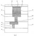
- the electrode metal 40is deposited over the full surface of the device, including over the passivation layer 30 and in the recess 38, as illustrated in Figure 5 .
- the electrode metalmay be a single layer, for example of Ta or Ti, a nitride for example TaN or TiN, or a multilayer for example Ta/TaN or Ti/TiN.
- Another CMP processis used to etch and/or polish away the electrode metal 40 from above the passivation layer 30 and hence to leave the electrode metal only in the recess 38 at the top of the via, flush (level) with the surface of the passivation layer 30 as shown in Figure 6 , forming the finished electrode 42.
- a biocompatible dielectric layer 44is then deposited over the complete surface.
- the dielectric layermay be, for example, of TiO 2 , Ta 2 O 5 , SiO 2 , SiN or HfO 2 or combinations of these or other materials.
- a damascene processis used to form the biocompatible electrode in the recess at the top of the via.
- This processis a self-aligned process and this therefore ensures that the electrode 42 has exactly the same dimensions as the underlying W contact. This avoids the possibility of contamination caused by misalignment of the biocompatible electrode and the plug.
- Figures 7 and 8illustrate a second embodiment.
- the method of manufacturing a semiconductor device according to the second embodimentproceeds in the same way as in the first embodiment to the stage illustrated in Figure 3 .
- the next stepis to carry out a selective etch to form recess 38, but in the process illustrated with reference to Figures 7 and 8 the selective etch etches both the barrier layer 34 and the filling metal 36 to form recess 38.
- Processingthen proceeds as in the first embodiment to form electrode 42 and dielectric 44 to result in the finished semiconductor device illustrated in Figure 8 .
- Figure 9illustrates a third embodiment using a copper interconnect.
- the manufactureproceeds essentially as in the embodiment of Figure 1 to 6 , except that the material of the first and second interconnects 18, 28 is copper. Note however one difference; the second interconnect 28 is used to fill additionally the second via 24 and there is no separate plug in the second interconnect layer (this is the so-called dual damascene processing).
- the material of the filling metal 36is also copper.
- the choices for the barrier layer 34include not merely Ti or TiN but Ta, or TaN/Ta.
Landscapes
- Engineering & Computer Science (AREA)
- Physics & Mathematics (AREA)
- Condensed Matter Physics & Semiconductors (AREA)
- General Physics & Mathematics (AREA)
- Manufacturing & Machinery (AREA)
- Computer Hardware Design (AREA)
- Microelectronics & Electronic Packaging (AREA)
- Power Engineering (AREA)
- Chemical & Material Sciences (AREA)
- Chemical Kinetics & Catalysis (AREA)
- General Chemical & Material Sciences (AREA)
- Internal Circuitry In Semiconductor Integrated Circuit Devices (AREA)
Description
- The invention relates to a method of making biocompatible electrodes.
- Electrodes for biological applications increasingly need to be included in semiconductor devices manufactured with modern semiconductor processing, especially complementary metal oxide semiconductor (CMOS) devices manufactured using CMOS processing techniques.
- An existing process for manufacturing an electrode for a biosensor is described inEversmann et al, CMOS Biosensor Array for Extracellular Recording of Neural Activity, IEEE Journal of Solid-State Circuits,),
- After completing a standard CMOS process to form devices, two metal layers, with a nitride passivation and a tungsten via, an additional process is used to form the additional sensor electrode. The surface is planarised, and a 50nm thick Ti/Pt stack is deposited and patterned using a liftoff process. The stack is used both as the sensor electrodes and as an adhesion layer for the bond pads. A 40nm sensor dielectric of TiO2, ZrO2, TiO2, ZrO2, and TiO2 is formed by sputtering to protect the biocompatible electrode. The sensor dielectric is removed over the bond pads.
- An alternative process for the manufacture of electrodes is proposed inFranz Hofmann et al, Technology Aspects of a CMOS Neuro-Sensor: Back End Process and Packaging, 33rd European conference on European Solid-State Device Research, 2003, 16-18 September 2003, pages 167 to 170.
- In this process, the conventional CMOS process is used and ends with a nitride passivation layer over a silicon dioxide layer. Then, to manufacture the electrodes a via is formed to the top layer of metallization, and filled with a Ti/TiN barrier layer and tungsten. Then, a CMP process is used to etch back to the nitride passivation layer. A Cr adhesion layer is followed by a Pt electrode layer and patterned using a lift-off process. TiO2 and/or ZrO2 are then deposited by sputtering. At the contact pads, but not the biocompatible electrodes, the TiO2 is etched away and a gold contact evaporated.
- A downside with both of these processes is that additional lithography and etching steps are required to manufacture the biocompatible electrodes which leads to expensive manufacturing costs.
- Further, the use of some metals are not compatible with modern CMOS processing. This applies in particular to platinum and gold. In particular, processing using platinum is normally only possible in older fabs intended for bipolar processing with wafer diameters up to 6 inch.
- Accordingly, there is a need for alternative processes for manufacturing biocompatible electrodes which is compatible with CMOS processing.
WO 00/75982 - According to the invention there is provided a method according to claim 1.
- By using the method according to the invention, the biocompatible electrode is formed with no lithography steps at all (after forming the via) and so the process is cheaper than those proposed before.
- The inventors have realized that a further problem occurs with the lithography step used to pattern the biocompatible electrode in the prior art approaches discussed above. If the lithography is slightly misaligned with the contact then some of the contact may be exposed after the manufacture of the electrode which can lead to contamination issues. In contrast, using the method proposed, the method is self aligned. This minimises contamination and overlay issues.
- The method is compatible with modern CMOS processes, including both processes with copper-based interconnects and aluminium-based interconnects.
- A further benefit is that the electrode is completely planar. This avoids stress at corners where subsequent dielectrics are deposited, improving reliability.
- Embodiments of the invention will now be described, purely by way of example, with reference to the accompanying drawings, in which:
Figures 1 to 6 illustrate steps in the manufacture of a semiconductor device according to a first embodiment of the invention;Figures 7 and8 illustrate steps in the manufacture of a semiconductor device according to a second embodiment of the invention; andFigure 9 illustrates a semiconductor device according to a third embodiment of the invention.- The figures are not to scale. Like or similar components are given the same reference numbers in the different Figures, and the corresponding description is not repeated.
- Referring to
Figure 1 , a conventional CMOS process results in a semiconductor device having asubstrate 10 with transistors and other devices formed within and on it. For clarity, these are not shown. - A number of interconnection layers are then formed. A first interconnection layer is formed of
insulator 12, typically silicon dioxide, having avia 14 formed through the insulator filled with aplug 16, here tungsten. A first layer ofaluminium interconnect 18 is provided above theplug 16. Thealuminium interconnect 18 extends across thesubstrate 10. - Similarly, a second interconnection layer is formed in the same way, namely with
insulator 22, via 24,plug 26 and interconnect 28. In the embodiment, theinterconnect 28 in the second layer is the highest level of interconnect and so will be referred to as the upper interconnect layer. - A
passivation layer 30 is then formed over the second interconnection layer withupper surface 31. Thepassivation layer 30 is insulating, and may be of silicon dioxide, silicon nitride, silicon carbide or a combination. In the preferred embodiment, the passivation layer is in fact a stack of SiC, followed by SiO2 followed by Si3N4; this stack may be referred to as the passivation stack. This results in the arrangement shown inFigure 1 . - Processing to form the biocompatible electrode then begins by forming a
via 32 through the passivation layer to theupper interconnect layer 28. This involves a lithographic step, to define the via. Typically, photoresist may be deposited and patterned to expose part of the passivation layer and a dry etching step carried out to etch through to the aluminium. Then, the photoresist is removed, as illustrated inFigure 2 . - A
barrier layer 34 is then deposited over the whole surface ofpassivation layer 30 and in thevia 32, using a process with good step coverage. Thebarrier layer 34 may be, for example a Ti/TiN barrier layer or a Ti/W barrier layer, both of which are fully compatible with CMOS processing. - Then, filling
metal 36, in the embodiment tungsten, is deposited over the whole surface, including in thevia 34. A conventional chemical mechanical polishing (CMP) step using a CMP tool then planarises the surface by etching and polishing away the fillingmetal 36 andbarrier layer 34 above thepassivation layer 30, leaving thebarrier layer 34 and filling metal present only in the via. This step leaves the top of the fillingmetal plug 36 level with the top of thepassivation layer 30 as illustrated inFigure 3 . - A further selective etch is then carried out to etch away the filling metal in the via, creating a
recess 38 as illustrated inFigure 4 , below the level of theupper surface 31. In this embodiment, the selective etch does not etch away thebarrier layer 34. - The particular etch selected in the embodiment is a H2O2 (hydrogen peroxide) etch. Normally, this would give a low etch rate which would reduce the process speed excessively. However, in the embodiment the H2O2 is supplied in the CMP tool previously used for the CMP step. The use of the CMP tool allows constant fresh H2O2 to be delivered to the surface of the wafer and allows constant removal of the dissolved W. The inventors have accordingly been able to achieve etch rates of 90nm/min and up using this H2O2 etch, much higher than would be expected by a conventional wet etch step using H2O2. Moreover, the use of the same tool as in the previous step is extremely efficient since it does not require moving the device at all.
- Further, note that by avoiding a dry etch at this stage there is no risk of damaging the dielectric in the
passivation layer 30. - Next, the
electrode metal 40 is deposited over the full surface of the device, including over thepassivation layer 30 and in therecess 38, as illustrated inFigure 5 . The electrode metal may be a single layer, for example of Ta or Ti, a nitride for example TaN or TiN, or a multilayer for example Ta/TaN or Ti/TiN. - After depositing the
electrode metal 40 another CMP process is used to etch and/or polish away theelectrode metal 40 from above thepassivation layer 30 and hence to leave the electrode metal only in therecess 38 at the top of the via, flush (level) with the surface of thepassivation layer 30 as shown inFigure 6 , forming thefinished electrode 42. - A
biocompatible dielectric layer 44 is then deposited over the complete surface. The dielectric layer may be, for example, of TiO2, Ta2O5, SiO2, SiN or HfO2 or combinations of these or other materials. - Thus, a damascene process is used to form the biocompatible electrode in the recess at the top of the via. This process is a self-aligned process and this therefore ensures that the
electrode 42 has exactly the same dimensions as the underlying W contact. This avoids the possibility of contamination caused by misalignment of the biocompatible electrode and the plug. - The possibility of avoiding the use of Au and Pt enables integration of the method on existing CMOS processing fabs, including those using copper interconnect.
Figures 7 and8 illustrate a second embodiment. The method of manufacturing a semiconductor device according to the second embodiment proceeds in the same way as in the first embodiment to the stage illustrated inFigure 3 .- The next step is to carry out a selective etch to form
recess 38, but in the process illustrated with reference toFigures 7 and8 the selective etch etches both thebarrier layer 34 and the fillingmetal 36 to formrecess 38. - Processing then proceeds as in the first embodiment to form
electrode 42 and dielectric 44 to result in the finished semiconductor device illustrated inFigure 8 . - The embodiments describe above relate to semiconductor devices using aluminium interconnect. However, the invention is also applicable to CMOS devices using other forms of interconnect, such as copper.
Figure 9 illustrates a third embodiment using a copper interconnect. In this embodiment, the manufacture proceeds essentially as in the embodiment ofFigure 1 to 6 , except that the material of the first andsecond interconnects second interconnect 28 is used to fill additionally the second via 24 and there is no separate plug in the second interconnect layer (this is the so-called dual damascene processing).- In the embodiment illustrated in
Figure 9 , the material of the fillingmetal 36 is also copper. In this case, the choices for thebarrier layer 34 include not merely Ti or TiN but Ta, or TaN/Ta. - Although in the
Figure 9 embodiment aCu filling metal 36 is used with copper interconnects, other possibilities for fillingmetal 36 exist, such as tungsten. - The above embodiments are all described with reference to a semiconductor device with two metallisation layers. However, the invention is equally applicable to semiconductor devices with only a single metallisation layer, as well as to semiconductor devices with more than two metallisation layers.
Claims (6)
- A method of manufacturing an electrode on a semiconductor device having a dielectric layer (30) above at least one metallisation layer (28), the method comprising:etching a via (32) in the dielectric layer (30) exposing the metallisation layer (28);depositing filling metal (36);etching back the filling metal using chemical mechanical polishing to remove the metal from the surface of the dielectric layer and to leave the metal in the via level with the top of the dielectric layer (30);carrying out a further etch to etch back the filling metal (36) in the via to form a recess (38) in the via;depositing an electrode metal (40) over the surface of the dielectric and in the recess in the via; andetching back the electrode metal (40) using chemical mechanical polishing to remove the electrode metal from the surface of the dielectric layer and to leave the electrode metal in the via to form the electrode (42);wherein the step of etching back the filling metal (36) using chemical mechanical polishing uses a chemical mechanical polishing tool; andcharacterised in that the step of carrying out a further etch to etch back the metal in the via to form a recess (38) includes supplying a wet etch solution through the said chemical mechanical polishing tool.
- A method according to claim 1 using a wet etch solution of hydrogen peroxide.
- A method according to any preceding claim further comprising forming a dielectric layer (44) over the electrode (42).
- A method according to any preceding claim wherein the electrode metal (40) is of at least one of Ta, Ti, TaN and TiN.
- A method according to any preceding claim wherein the at least one metallisation layer (28) is of copper or an alloy of copper and the filling metal (36) is tungsten or copper.
- A method according to any of claims 1 to 5 wherein the at least one metallisation layer (28) is of aluminium or an alloy of aluminium and the filling metal (36) is tungsten.
Priority Applications (1)
| Application Number | Priority Date | Filing Date | Title |
|---|---|---|---|
| EP09756821.6AEP2345069B1 (en) | 2008-10-27 | 2009-10-26 | Method of manufacturing a biocompatible electrode |
Applications Claiming Priority (3)
| Application Number | Priority Date | Filing Date | Title |
|---|---|---|---|
| EP08105674 | 2008-10-27 | ||
| PCT/IB2009/054736WO2010049881A1 (en) | 2008-10-27 | 2009-10-26 | Biocompatible electrodes |
| EP09756821.6AEP2345069B1 (en) | 2008-10-27 | 2009-10-26 | Method of manufacturing a biocompatible electrode |
Publications (2)
| Publication Number | Publication Date |
|---|---|
| EP2345069A1 EP2345069A1 (en) | 2011-07-20 |
| EP2345069B1true EP2345069B1 (en) | 2016-02-17 |
Family
ID=41527795
Family Applications (1)
| Application Number | Title | Priority Date | Filing Date |
|---|---|---|---|
| EP09756821.6ANot-in-forceEP2345069B1 (en) | 2008-10-27 | 2009-10-26 | Method of manufacturing a biocompatible electrode |
Country Status (4)
| Country | Link |
|---|---|
| US (1) | US9281239B2 (en) |
| EP (1) | EP2345069B1 (en) |
| CN (1) | CN102203935A (en) |
| WO (1) | WO2010049881A1 (en) |
Cited By (1)
| Publication number | Priority date | Publication date | Assignee | Title |
|---|---|---|---|---|
| EP3503169A1 (en)* | 2017-12-22 | 2019-06-26 | Applied Materials, Inc. | Methods of etching a tungsten layer |
Families Citing this family (25)
| Publication number | Priority date | Publication date | Assignee | Title |
|---|---|---|---|---|
| CN103646848B (en) | 2004-06-04 | 2018-06-05 | 伊利诺伊大学评议会 | The method of assembling printable semiconductor elements and manufacture electronic device |
| US8886334B2 (en) | 2008-10-07 | 2014-11-11 | Mc10, Inc. | Systems, methods, and devices using stretchable or flexible electronics for medical applications |
| JP5646492B2 (en) | 2008-10-07 | 2014-12-24 | エムシー10 インコーポレイテッドMc10,Inc. | Stretchable integrated circuit and device with sensor array |
| US8389862B2 (en) | 2008-10-07 | 2013-03-05 | Mc10, Inc. | Extremely stretchable electronics |
| WO2011041727A1 (en) | 2009-10-01 | 2011-04-07 | Mc10, Inc. | Protective cases with integrated electronics |
| US9936574B2 (en) | 2009-12-16 | 2018-04-03 | The Board Of Trustees Of The University Of Illinois | Waterproof stretchable optoelectronics |
| US10918298B2 (en) | 2009-12-16 | 2021-02-16 | The Board Of Trustees Of The University Of Illinois | High-speed, high-resolution electrophysiology in-vivo using conformal electronics |
| US10441185B2 (en) | 2009-12-16 | 2019-10-15 | The Board Of Trustees Of The University Of Illinois | Flexible and stretchable electronic systems for epidermal electronics |
| EP2547258B1 (en) | 2010-03-17 | 2015-08-05 | The Board of Trustees of the University of Illionis | Implantable biomedical devices on bioresorbable substrates |
| EP2492239B1 (en)* | 2011-02-22 | 2020-08-26 | Sciosense B.V. | Integrated circuit with sensor and method of manufacturing such an integrated circuit |
| US9765934B2 (en) | 2011-05-16 | 2017-09-19 | The Board Of Trustees Of The University Of Illinois | Thermally managed LED arrays assembled by printing |
| EP2527824B1 (en) | 2011-05-27 | 2016-05-04 | ams international AG | Integrated circuit with moisture sensor and method of manufacturing such an integrated circuit |
| JP2014523633A (en) | 2011-05-27 | 2014-09-11 | エムシー10 インコーポレイテッド | Electronic, optical and / or mechanical devices and systems and methods of manufacturing these devices and systems |
| WO2012167096A2 (en) | 2011-06-03 | 2012-12-06 | The Board Of Trustees Of The University Of Illinois | Conformable actively multiplexed high-density surface electrode array for brain interfacing |
| KR101979354B1 (en) | 2011-12-01 | 2019-08-29 | 더 보오드 오브 트러스티스 오브 더 유니버시티 오브 일리노이즈 | Transient devices designed to undergo programmable transformations |
| JP2015521303A (en) | 2012-03-30 | 2015-07-27 | ザ ボード オブ トラスティーズ オブ ザ ユニヴァーシ | An electronic device that can be attached to the surface and can be attached to an accessory |
| US9171794B2 (en) | 2012-10-09 | 2015-10-27 | Mc10, Inc. | Embedding thin chips in polymer |
| EP2738551B1 (en)* | 2012-12-03 | 2015-03-18 | Nxp B.V. | Biosensor module comprising a biocompatible electrode |
| US8940597B2 (en)* | 2013-03-11 | 2015-01-27 | Taiwan Semiconductor Manufacturing Co., Ltd. | In-situ metal gate recess process for self-aligned contact application |
| MX2017015587A (en) | 2015-06-01 | 2018-08-23 | Univ Illinois | Alternative approach to uv sensing. |
| AU2016270807A1 (en) | 2015-06-01 | 2017-12-14 | The Board Of Trustees Of The University Of Illinois | Miniaturized electronic systems with wireless power and near-field communication capabilities |
| US10925543B2 (en) | 2015-11-11 | 2021-02-23 | The Board Of Trustees Of The University Of Illinois | Bioresorbable silicon electronics for transient implants |
| DE102019120795A1 (en)* | 2018-09-28 | 2020-04-02 | Taiwan Semiconductor Manufacturing Co., Ltd. | THROUGH CONTACTS WITH METAL CAPS UNDER THE CONDUCTIVE CABLES UNDER |
| US11282788B2 (en) | 2019-07-25 | 2022-03-22 | International Business Machines Corporation | Interconnect and memory structures formed in the BEOL |
| US11195751B2 (en) | 2019-09-13 | 2021-12-07 | International Business Machines Corporation | Bilayer barrier for interconnect and memory structures formed in the BEOL |
Family Cites Families (21)
| Publication number | Priority date | Publication date | Assignee | Title |
|---|---|---|---|---|
| JP3304754B2 (en)* | 1996-04-11 | 2002-07-22 | 三菱電機株式会社 | Multistage embedded wiring structure of integrated circuit |
| US6001269A (en)* | 1997-05-20 | 1999-12-14 | Rodel, Inc. | Method for polishing a composite comprising an insulator, a metal, and titanium |
| US6211087B1 (en)* | 1998-06-29 | 2001-04-03 | Vlsi Technology, Inc. | Chemical wet etch removal of underlayer material after performing chemical mechanical polishing on a primary layer |
| US6395607B1 (en) | 1999-06-09 | 2002-05-28 | Alliedsignal Inc. | Integrated circuit fabrication method for self-aligned copper diffusion barrier |
| JP2001077118A (en)* | 1999-06-30 | 2001-03-23 | Toshiba Corp | Semiconductor device and method of manufacturing the same |
| US6251786B1 (en)* | 1999-09-07 | 2001-06-26 | Chartered Semiconductor Manufacturing Ltd. | Method to create a copper dual damascene structure with less dishing and erosion |
| US6274499B1 (en)* | 1999-11-19 | 2001-08-14 | Chartered Semiconductor Manufacturing Ltd. | Method to avoid copper contamination during copper etching and CMP |
| JP3907151B2 (en)* | 2000-01-25 | 2007-04-18 | 株式会社東芝 | Manufacturing method of semiconductor device |
| JP2001291720A (en)* | 2000-04-05 | 2001-10-19 | Hitachi Ltd | Semiconductor integrated circuit device and method of manufacturing semiconductor integrated circuit device |
| US6376353B1 (en)* | 2000-07-03 | 2002-04-23 | Chartered Semiconductor Manufacturing Ltd. | Aluminum and copper bimetallic bond pad scheme for copper damascene interconnects |
| JP2004006499A (en)* | 2002-05-31 | 2004-01-08 | Mitsubishi Electric Corp | Semiconductor manufacturing apparatus, polishing liquid supply apparatus, method for detecting characteristics of polishing liquid, and method for manufacturing semiconductor device |
| US6670274B1 (en)* | 2002-10-01 | 2003-12-30 | Taiwan Semiconductor Manufacturing Company | Method of forming a copper damascene structure comprising a recessed copper-oxide-free initial copper structure |
| KR20040060563A (en)* | 2002-12-30 | 2004-07-06 | 동부전자 주식회사 | Manufacture method and structure of semiconductor element |
| WO2004072332A1 (en)* | 2003-02-12 | 2004-08-26 | Ebara Corporation | Polishing fluid, method of polishing, and polishing apparatus |
| US7060619B2 (en)* | 2003-03-04 | 2006-06-13 | Infineon Technologies Ag | Reduction of the shear stress in copper via's in organic interlayer dielectric material |
| US7071564B1 (en)* | 2004-03-04 | 2006-07-04 | Advanced Micro Devices, Inc. | Composite tantalum capped inlaid copper with reduced electromigration and reduced stress migration |
| US7119018B2 (en)* | 2004-07-09 | 2006-10-10 | International Buisness Machines Corporation | Copper conductor |
| US7105445B2 (en)* | 2005-01-14 | 2006-09-12 | International Business Machines Corporation | Interconnect structures with encasing cap and methods of making thereof |
| US7387961B2 (en)* | 2005-01-31 | 2008-06-17 | Taiwan Semiconductor Manufacturing Co., Ltd | Dual damascene with via liner |
| US7348672B2 (en)* | 2005-07-07 | 2008-03-25 | Taiwan Semiconductor Manufacturing Co., Ltd. | Interconnects with improved reliability |
| US20070072311A1 (en)* | 2005-09-28 | 2007-03-29 | Northern Lights Semiconductor Corp. | Interconnect for a GMR Stack Layer and an Underlying Conducting Layer |
- 2009
- 2009-10-26EPEP09756821.6Apatent/EP2345069B1/ennot_activeNot-in-force
- 2009-10-26CNCN2009801421467Apatent/CN102203935A/enactivePending
- 2009-10-26WOPCT/IB2009/054736patent/WO2010049881A1/enactiveApplication Filing
- 2009-10-26USUS13/126,057patent/US9281239B2/ennot_activeExpired - Fee Related
Cited By (1)
| Publication number | Priority date | Publication date | Assignee | Title |
|---|---|---|---|---|
| EP3503169A1 (en)* | 2017-12-22 | 2019-06-26 | Applied Materials, Inc. | Methods of etching a tungsten layer |
Also Published As
| Publication number | Publication date |
|---|---|
| US20110207239A1 (en) | 2011-08-25 |
| EP2345069A1 (en) | 2011-07-20 |
| CN102203935A (en) | 2011-09-28 |
| WO2010049881A1 (en) | 2010-05-06 |
| US9281239B2 (en) | 2016-03-08 |
Similar Documents
| Publication | Publication Date | Title |
|---|---|---|
| EP2345069B1 (en) | Method of manufacturing a biocompatible electrode | |
| US11251131B2 (en) | Copper contact plugs with barrier layers | |
| US6528884B1 (en) | Conformal atomic liner layer in an integrated circuit interconnect | |
| US7220652B2 (en) | Metal-insulator-metal capacitor and interconnecting structure | |
| US6734559B1 (en) | Self-aligned semiconductor interconnect barrier and manufacturing method therefor | |
| TWI473233B (en) | Semiconductor device having a copper plug | |
| US20070063352A1 (en) | Routing under bond pad for the replacement of an interconnect layer | |
| US20040238962A1 (en) | Semiconductor device including metal interconnection and metal resistor and method of manufacturing the same | |
| US7242102B2 (en) | Bond pad structure for copper metallization having increased reliability and method for fabricating same | |
| US7586142B2 (en) | Semiconductor device having metal-insulator-metal capacitor and method of fabricating the same | |
| US6406996B1 (en) | Sub-cap and method of manufacture therefor in integrated circuit capping layers | |
| US20070023868A1 (en) | Method of forming copper metal line and semiconductor device including the same | |
| EP1330842B1 (en) | Low temperature hillock suppression method in integrated circuit interconnects | |
| US20050266679A1 (en) | Barrier structure for semiconductor devices | |
| US6469385B1 (en) | Integrated circuit with dielectric diffusion barrier layer formed between interconnects and interlayer dielectric layers | |
| US6674170B1 (en) | Barrier metal oxide interconnect cap in integrated circuits | |
| US6472757B2 (en) | Conductor reservoir volume for integrated circuit interconnects | |
| US20120074572A1 (en) | Semiconductor structure and method for making same | |
| US8697565B2 (en) | Shallow via formation by oxidation | |
| KR20080047541A (en) | How to Form a Capping Layer on a Semiconductor Device | |
| US6455938B1 (en) | Integrated circuit interconnect shunt layer | |
| US6979903B1 (en) | Integrated circuit with dielectric diffusion barrier layer formed between interconnects and interlayer dielectric layers | |
| US6403474B1 (en) | Controlled anneal conductors for integrated circuit interconnects | |
| CN220934078U (en) | Integrated chip | |
| US20070120264A1 (en) | A semiconductor having a copper-based metallization stack with a last aluminum metal line layer |
Legal Events
| Date | Code | Title | Description |
|---|---|---|---|
| PUAI | Public reference made under article 153(3) epc to a published international application that has entered the european phase | Free format text:ORIGINAL CODE: 0009012 | |
| 17P | Request for examination filed | Effective date:20110527 | |
| AK | Designated contracting states | Kind code of ref document:A1 Designated state(s):AT BE BG CH CY CZ DE DK EE ES FI FR GB GR HR HU IE IS IT LI LT LU LV MC MK MT NL NO PL PT RO SE SI SK SM TR | |
| AX | Request for extension of the european patent | Extension state:AL BA RS | |
| DAX | Request for extension of the european patent (deleted) | ||
| RIC1 | Information provided on ipc code assigned before grant | Ipc:G01N 27/403 20060101ALI20150720BHEP Ipc:H01L 21/768 20060101AFI20150720BHEP Ipc:H01L 21/3213 20060101ALI20150720BHEP | |
| GRAP | Despatch of communication of intention to grant a patent | Free format text:ORIGINAL CODE: EPIDOSNIGR1 | |
| INTG | Intention to grant announced | Effective date:20150831 | |
| GRAS | Grant fee paid | Free format text:ORIGINAL CODE: EPIDOSNIGR3 | |
| GRAA | (expected) grant | Free format text:ORIGINAL CODE: 0009210 | |
| AK | Designated contracting states | Kind code of ref document:B1 Designated state(s):AT BE BG CH CY CZ DE DK EE ES FI FR GB GR HR HU IE IS IT LI LT LU LV MC MK MT NL NO PL PT RO SE SI SK SM TR | |
| REG | Reference to a national code | Ref country code:GB Ref legal event code:FG4D | |
| REG | Reference to a national code | Ref country code:CH Ref legal event code:EP | |
| REG | Reference to a national code | Ref country code:IE Ref legal event code:FG4D | |
| REG | Reference to a national code | Ref country code:AT Ref legal event code:REF Ref document number:775985 Country of ref document:AT Kind code of ref document:T Effective date:20160315 | |
| REG | Reference to a national code | Ref country code:DE Ref legal event code:R096 Ref document number:602009036346 Country of ref document:DE | |
| REG | Reference to a national code | Ref country code:NL Ref legal event code:MP Effective date:20160217 | |
| REG | Reference to a national code | Ref country code:LT Ref legal event code:MG4D | |
| REG | Reference to a national code | Ref country code:AT Ref legal event code:MK05 Ref document number:775985 Country of ref document:AT Kind code of ref document:T Effective date:20160217 | |
| PG25 | Lapsed in a contracting state [announced via postgrant information from national office to epo] | Ref country code:ES Free format text:LAPSE BECAUSE OF FAILURE TO SUBMIT A TRANSLATION OF THE DESCRIPTION OR TO PAY THE FEE WITHIN THE PRESCRIBED TIME-LIMIT Effective date:20160217 Ref country code:IT Free format text:LAPSE BECAUSE OF FAILURE TO SUBMIT A TRANSLATION OF THE DESCRIPTION OR TO PAY THE FEE WITHIN THE PRESCRIBED TIME-LIMIT Effective date:20160217 Ref country code:FI Free format text:LAPSE BECAUSE OF FAILURE TO SUBMIT A TRANSLATION OF THE DESCRIPTION OR TO PAY THE FEE WITHIN THE PRESCRIBED TIME-LIMIT Effective date:20160217 Ref country code:NO Free format text:LAPSE BECAUSE OF FAILURE TO SUBMIT A TRANSLATION OF THE DESCRIPTION OR TO PAY THE FEE WITHIN THE PRESCRIBED TIME-LIMIT Effective date:20160517 Ref country code:GR Free format text:LAPSE BECAUSE OF FAILURE TO SUBMIT A TRANSLATION OF THE DESCRIPTION OR TO PAY THE FEE WITHIN THE PRESCRIBED TIME-LIMIT Effective date:20160518 | |
| PG25 | Lapsed in a contracting state [announced via postgrant information from national office to epo] | Ref country code:LV Free format text:LAPSE BECAUSE OF FAILURE TO SUBMIT A TRANSLATION OF THE DESCRIPTION OR TO PAY THE FEE WITHIN THE PRESCRIBED TIME-LIMIT Effective date:20160217 Ref country code:PL Free format text:LAPSE BECAUSE OF FAILURE TO SUBMIT A TRANSLATION OF THE DESCRIPTION OR TO PAY THE FEE WITHIN THE PRESCRIBED TIME-LIMIT Effective date:20160217 Ref country code:SE Free format text:LAPSE BECAUSE OF FAILURE TO SUBMIT A TRANSLATION OF THE DESCRIPTION OR TO PAY THE FEE WITHIN THE PRESCRIBED TIME-LIMIT Effective date:20160217 Ref country code:LT Free format text:LAPSE BECAUSE OF FAILURE TO SUBMIT A TRANSLATION OF THE DESCRIPTION OR TO PAY THE FEE WITHIN THE PRESCRIBED TIME-LIMIT Effective date:20160217 Ref country code:NL Free format text:LAPSE BECAUSE OF FAILURE TO SUBMIT A TRANSLATION OF THE DESCRIPTION OR TO PAY THE FEE WITHIN THE PRESCRIBED TIME-LIMIT Effective date:20160217 Ref country code:AT Free format text:LAPSE BECAUSE OF FAILURE TO SUBMIT A TRANSLATION OF THE DESCRIPTION OR TO PAY THE FEE WITHIN THE PRESCRIBED TIME-LIMIT Effective date:20160217 Ref country code:PT Free format text:LAPSE BECAUSE OF FAILURE TO SUBMIT A TRANSLATION OF THE DESCRIPTION OR TO PAY THE FEE WITHIN THE PRESCRIBED TIME-LIMIT Effective date:20160617 | |
| PG25 | Lapsed in a contracting state [announced via postgrant information from national office to epo] | Ref country code:EE Free format text:LAPSE BECAUSE OF FAILURE TO SUBMIT A TRANSLATION OF THE DESCRIPTION OR TO PAY THE FEE WITHIN THE PRESCRIBED TIME-LIMIT Effective date:20160217 Ref country code:DK Free format text:LAPSE BECAUSE OF FAILURE TO SUBMIT A TRANSLATION OF THE DESCRIPTION OR TO PAY THE FEE WITHIN THE PRESCRIBED TIME-LIMIT Effective date:20160217 | |
| REG | Reference to a national code | Ref country code:DE Ref legal event code:R097 Ref document number:602009036346 Country of ref document:DE | |
| PG25 | Lapsed in a contracting state [announced via postgrant information from national office to epo] | Ref country code:SM Free format text:LAPSE BECAUSE OF FAILURE TO SUBMIT A TRANSLATION OF THE DESCRIPTION OR TO PAY THE FEE WITHIN THE PRESCRIBED TIME-LIMIT Effective date:20160217 Ref country code:SK Free format text:LAPSE BECAUSE OF FAILURE TO SUBMIT A TRANSLATION OF THE DESCRIPTION OR TO PAY THE FEE WITHIN THE PRESCRIBED TIME-LIMIT Effective date:20160217 Ref country code:CZ Free format text:LAPSE BECAUSE OF FAILURE TO SUBMIT A TRANSLATION OF THE DESCRIPTION OR TO PAY THE FEE WITHIN THE PRESCRIBED TIME-LIMIT Effective date:20160217 Ref country code:RO Free format text:LAPSE BECAUSE OF FAILURE TO SUBMIT A TRANSLATION OF THE DESCRIPTION OR TO PAY THE FEE WITHIN THE PRESCRIBED TIME-LIMIT Effective date:20160217 | |
| PLBE | No opposition filed within time limit | Free format text:ORIGINAL CODE: 0009261 | |
| STAA | Information on the status of an ep patent application or granted ep patent | Free format text:STATUS: NO OPPOSITION FILED WITHIN TIME LIMIT | |
| PG25 | Lapsed in a contracting state [announced via postgrant information from national office to epo] | Ref country code:BE Free format text:LAPSE BECAUSE OF FAILURE TO SUBMIT A TRANSLATION OF THE DESCRIPTION OR TO PAY THE FEE WITHIN THE PRESCRIBED TIME-LIMIT Effective date:20160217 | |
| 26N | No opposition filed | Effective date:20161118 | |
| PG25 | Lapsed in a contracting state [announced via postgrant information from national office to epo] | Ref country code:SI Free format text:LAPSE BECAUSE OF FAILURE TO SUBMIT A TRANSLATION OF THE DESCRIPTION OR TO PAY THE FEE WITHIN THE PRESCRIBED TIME-LIMIT Effective date:20160217 Ref country code:BG Free format text:LAPSE BECAUSE OF FAILURE TO SUBMIT A TRANSLATION OF THE DESCRIPTION OR TO PAY THE FEE WITHIN THE PRESCRIBED TIME-LIMIT Effective date:20160517 | |
| REG | Reference to a national code | Ref country code:CH Ref legal event code:PL | |
| GBPC | Gb: european patent ceased through non-payment of renewal fee | Effective date:20161026 | |
| REG | Reference to a national code | Ref country code:IE Ref legal event code:MM4A | |
| REG | Reference to a national code | Ref country code:FR Ref legal event code:ST Effective date:20170630 | |
| PG25 | Lapsed in a contracting state [announced via postgrant information from national office to epo] | Ref country code:LI Free format text:LAPSE BECAUSE OF NON-PAYMENT OF DUE FEES Effective date:20161031 Ref country code:FR Free format text:LAPSE BECAUSE OF NON-PAYMENT OF DUE FEES Effective date:20161102 Ref country code:GB Free format text:LAPSE BECAUSE OF NON-PAYMENT OF DUE FEES Effective date:20161026 Ref country code:CH Free format text:LAPSE BECAUSE OF NON-PAYMENT OF DUE FEES Effective date:20161031 | |
| PG25 | Lapsed in a contracting state [announced via postgrant information from national office to epo] | Ref country code:LU Free format text:LAPSE BECAUSE OF NON-PAYMENT OF DUE FEES Effective date:20161026 | |
| PG25 | Lapsed in a contracting state [announced via postgrant information from national office to epo] | Ref country code:IE Free format text:LAPSE BECAUSE OF NON-PAYMENT OF DUE FEES Effective date:20161026 | |
| PG25 | Lapsed in a contracting state [announced via postgrant information from national office to epo] | Ref country code:CY Free format text:LAPSE BECAUSE OF FAILURE TO SUBMIT A TRANSLATION OF THE DESCRIPTION OR TO PAY THE FEE WITHIN THE PRESCRIBED TIME-LIMIT Effective date:20160217 Ref country code:HU Free format text:LAPSE BECAUSE OF FAILURE TO SUBMIT A TRANSLATION OF THE DESCRIPTION OR TO PAY THE FEE WITHIN THE PRESCRIBED TIME-LIMIT; INVALID AB INITIO Effective date:20091026 | |
| PG25 | Lapsed in a contracting state [announced via postgrant information from national office to epo] | Ref country code:IS Free format text:LAPSE BECAUSE OF FAILURE TO SUBMIT A TRANSLATION OF THE DESCRIPTION OR TO PAY THE FEE WITHIN THE PRESCRIBED TIME-LIMIT Effective date:20160217 Ref country code:HR Free format text:LAPSE BECAUSE OF FAILURE TO SUBMIT A TRANSLATION OF THE DESCRIPTION OR TO PAY THE FEE WITHIN THE PRESCRIBED TIME-LIMIT Effective date:20160217 Ref country code:MC Free format text:LAPSE BECAUSE OF FAILURE TO SUBMIT A TRANSLATION OF THE DESCRIPTION OR TO PAY THE FEE WITHIN THE PRESCRIBED TIME-LIMIT Effective date:20160217 Ref country code:TR Free format text:LAPSE BECAUSE OF FAILURE TO SUBMIT A TRANSLATION OF THE DESCRIPTION OR TO PAY THE FEE WITHIN THE PRESCRIBED TIME-LIMIT Effective date:20160217 Ref country code:MK Free format text:LAPSE BECAUSE OF FAILURE TO SUBMIT A TRANSLATION OF THE DESCRIPTION OR TO PAY THE FEE WITHIN THE PRESCRIBED TIME-LIMIT Effective date:20160217 Ref country code:MT Free format text:LAPSE BECAUSE OF NON-PAYMENT OF DUE FEES Effective date:20161031 | |
| PGFP | Annual fee paid to national office [announced via postgrant information from national office to epo] | Ref country code:DE Payment date:20220920 Year of fee payment:14 | |
| REG | Reference to a national code | Ref country code:DE Ref legal event code:R119 Ref document number:602009036346 Country of ref document:DE | |
| PG25 | Lapsed in a contracting state [announced via postgrant information from national office to epo] | Ref country code:DE Free format text:LAPSE BECAUSE OF NON-PAYMENT OF DUE FEES Effective date:20240501 |