EP2341495B1 - Display Apparatus and Method of Driving Same - Google Patents
Display Apparatus and Method of Driving SameDownload PDFInfo
- Publication number
- EP2341495B1 EP2341495B1EP11156768.1AEP11156768AEP2341495B1EP 2341495 B1EP2341495 B1EP 2341495B1EP 11156768 AEP11156768 AEP 11156768AEP 2341495 B1EP2341495 B1EP 2341495B1
- Authority
- EP
- European Patent Office
- Prior art keywords
- potential
- signal
- drive transistor
- power supply
- lines
- Prior art date
- Legal status (The legal status is an assumption and is not a legal conclusion. Google has not performed a legal analysis and makes no representation as to the accuracy of the status listed.)
- Active
Links
Images


Classifications
- G—PHYSICS
- G09—EDUCATION; CRYPTOGRAPHY; DISPLAY; ADVERTISING; SEALS
- G09G—ARRANGEMENTS OR CIRCUITS FOR CONTROL OF INDICATING DEVICES USING STATIC MEANS TO PRESENT VARIABLE INFORMATION
- G09G3/00—Control arrangements or circuits, of interest only in connection with visual indicators other than cathode-ray tubes
- G09G3/20—Control arrangements or circuits, of interest only in connection with visual indicators other than cathode-ray tubes for presentation of an assembly of a number of characters, e.g. a page, by composing the assembly by combination of individual elements arranged in a matrix no fixed position being assigned to or needed to be assigned to the individual characters or partial characters
- G09G3/22—Control arrangements or circuits, of interest only in connection with visual indicators other than cathode-ray tubes for presentation of an assembly of a number of characters, e.g. a page, by composing the assembly by combination of individual elements arranged in a matrix no fixed position being assigned to or needed to be assigned to the individual characters or partial characters using controlled light sources
- G09G3/30—Control arrangements or circuits, of interest only in connection with visual indicators other than cathode-ray tubes for presentation of an assembly of a number of characters, e.g. a page, by composing the assembly by combination of individual elements arranged in a matrix no fixed position being assigned to or needed to be assigned to the individual characters or partial characters using controlled light sources using electroluminescent panels
- G09G3/32—Control arrangements or circuits, of interest only in connection with visual indicators other than cathode-ray tubes for presentation of an assembly of a number of characters, e.g. a page, by composing the assembly by combination of individual elements arranged in a matrix no fixed position being assigned to or needed to be assigned to the individual characters or partial characters using controlled light sources using electroluminescent panels semiconductive, e.g. using light-emitting diodes [LED]
- G09G3/3208—Control arrangements or circuits, of interest only in connection with visual indicators other than cathode-ray tubes for presentation of an assembly of a number of characters, e.g. a page, by composing the assembly by combination of individual elements arranged in a matrix no fixed position being assigned to or needed to be assigned to the individual characters or partial characters using controlled light sources using electroluminescent panels semiconductive, e.g. using light-emitting diodes [LED] organic, e.g. using organic light-emitting diodes [OLED]
- G09G3/3225—Control arrangements or circuits, of interest only in connection with visual indicators other than cathode-ray tubes for presentation of an assembly of a number of characters, e.g. a page, by composing the assembly by combination of individual elements arranged in a matrix no fixed position being assigned to or needed to be assigned to the individual characters or partial characters using controlled light sources using electroluminescent panels semiconductive, e.g. using light-emitting diodes [LED] organic, e.g. using organic light-emitting diodes [OLED] using an active matrix
- G09G3/3233—Control arrangements or circuits, of interest only in connection with visual indicators other than cathode-ray tubes for presentation of an assembly of a number of characters, e.g. a page, by composing the assembly by combination of individual elements arranged in a matrix no fixed position being assigned to or needed to be assigned to the individual characters or partial characters using controlled light sources using electroluminescent panels semiconductive, e.g. using light-emitting diodes [LED] organic, e.g. using organic light-emitting diodes [OLED] using an active matrix with pixel circuitry controlling the current through the light-emitting element
- G—PHYSICS
- G09—EDUCATION; CRYPTOGRAPHY; DISPLAY; ADVERTISING; SEALS
- G09G—ARRANGEMENTS OR CIRCUITS FOR CONTROL OF INDICATING DEVICES USING STATIC MEANS TO PRESENT VARIABLE INFORMATION
- G09G3/00—Control arrangements or circuits, of interest only in connection with visual indicators other than cathode-ray tubes
- G09G3/20—Control arrangements or circuits, of interest only in connection with visual indicators other than cathode-ray tubes for presentation of an assembly of a number of characters, e.g. a page, by composing the assembly by combination of individual elements arranged in a matrix no fixed position being assigned to or needed to be assigned to the individual characters or partial characters
- G09G3/22—Control arrangements or circuits, of interest only in connection with visual indicators other than cathode-ray tubes for presentation of an assembly of a number of characters, e.g. a page, by composing the assembly by combination of individual elements arranged in a matrix no fixed position being assigned to or needed to be assigned to the individual characters or partial characters using controlled light sources
- G09G3/30—Control arrangements or circuits, of interest only in connection with visual indicators other than cathode-ray tubes for presentation of an assembly of a number of characters, e.g. a page, by composing the assembly by combination of individual elements arranged in a matrix no fixed position being assigned to or needed to be assigned to the individual characters or partial characters using controlled light sources using electroluminescent panels
- G09G3/32—Control arrangements or circuits, of interest only in connection with visual indicators other than cathode-ray tubes for presentation of an assembly of a number of characters, e.g. a page, by composing the assembly by combination of individual elements arranged in a matrix no fixed position being assigned to or needed to be assigned to the individual characters or partial characters using controlled light sources using electroluminescent panels semiconductive, e.g. using light-emitting diodes [LED]
- H—ELECTRICITY
- H05—ELECTRIC TECHNIQUES NOT OTHERWISE PROVIDED FOR
- H05B—ELECTRIC HEATING; ELECTRIC LIGHT SOURCES NOT OTHERWISE PROVIDED FOR; CIRCUIT ARRANGEMENTS FOR ELECTRIC LIGHT SOURCES, IN GENERAL
- H05B33/00—Electroluminescent light sources
- H05B33/12—Light sources with substantially two-dimensional radiating surfaces
- G—PHYSICS
- G09—EDUCATION; CRYPTOGRAPHY; DISPLAY; ADVERTISING; SEALS
- G09G—ARRANGEMENTS OR CIRCUITS FOR CONTROL OF INDICATING DEVICES USING STATIC MEANS TO PRESENT VARIABLE INFORMATION
- G09G2300/00—Aspects of the constitution of display devices
- G09G2300/08—Active matrix structure, i.e. with use of active elements, inclusive of non-linear two terminal elements, in the pixels together with light emitting or modulating elements
- G09G2300/0809—Several active elements per pixel in active matrix panels
- G09G2300/0819—Several active elements per pixel in active matrix panels used for counteracting undesired variations, e.g. feedback or autozeroing
- G—PHYSICS
- G09—EDUCATION; CRYPTOGRAPHY; DISPLAY; ADVERTISING; SEALS
- G09G—ARRANGEMENTS OR CIRCUITS FOR CONTROL OF INDICATING DEVICES USING STATIC MEANS TO PRESENT VARIABLE INFORMATION
- G09G2300/00—Aspects of the constitution of display devices
- G09G2300/08—Active matrix structure, i.e. with use of active elements, inclusive of non-linear two terminal elements, in the pixels together with light emitting or modulating elements
- G09G2300/0809—Several active elements per pixel in active matrix panels
- G09G2300/0842—Several active elements per pixel in active matrix panels forming a memory circuit, e.g. a dynamic memory with one capacitor
- G09G2300/0861—Several active elements per pixel in active matrix panels forming a memory circuit, e.g. a dynamic memory with one capacitor with additional control of the display period without amending the charge stored in a pixel memory, e.g. by means of additional select electrodes
- G09G2300/0866—Several active elements per pixel in active matrix panels forming a memory circuit, e.g. a dynamic memory with one capacitor with additional control of the display period without amending the charge stored in a pixel memory, e.g. by means of additional select electrodes by means of changes in the pixel supply voltage
- G—PHYSICS
- G09—EDUCATION; CRYPTOGRAPHY; DISPLAY; ADVERTISING; SEALS
- G09G—ARRANGEMENTS OR CIRCUITS FOR CONTROL OF INDICATING DEVICES USING STATIC MEANS TO PRESENT VARIABLE INFORMATION
- G09G2320/00—Control of display operating conditions
- G09G2320/04—Maintaining the quality of display appearance
- G09G2320/043—Preventing or counteracting the effects of ageing
Definitions
- the present inventionrelates to a display apparatus such as an active-matrix display apparatus having light-emitting devices as pixels thereof, and a method of driving such a display apparatus.
- An organic EL deviceis a device utilizing a phenomenon in which an organic thin film emits light under an electric field.
- the organic EL devicehas a low power requirement because it can be energized under a low voltage of 10 V or lower. Since the organic EL device is a self-emission device for emitting light by itself, it requires no illuminating members, and hence can be lightweight and of a low profile.
- the organic EL devicedoes not produce an image lag when it displays moving images because the response speed thereof is of a very high value of about several ⁇ s.
- active-matrix display apparatusincluding thin-film transistors integrated in respective pixels as drive elements are particularly under active development.
- Active-matrix flat self-emission display apparatusare disclosed in Japanese laid-open patent publication Nos. 2003-255856 , 2003-271095 , 2004-133240 , 2004-029791 , and 2004-093682 .
- transistors for driving light-emitting deviceshave various threshold voltages and mobilities due to fabrication process variations.
- the characteristics of the organic EL devicestend to vary with time.
- Such characteristic variations of the drive transistors and characteristic variations of the organic EL devicesadversely affect the light emission luminance.
- existing pixel circuits with a correcting functionare complex in structure as they demand an interconnect for supplying a correcting potential, a switching transistor, and a switching pulse. Because each of the pixel circuits has many components, they have presented obstacles to efforts to achieve higher-definition display.
- US 2005/0206590describes an image display apparatus that comprises a pixel having a drive transistor and a pixel display element which are connected in series between a first power line and a second power line, a holding capacitor connected to a gate electrode of the drive transistor, and a selection transistor connected between a signal line and the gate electrode of the drive transistor.
- a selection transistorWhen the selection transistor is turned on, gradation pixel data is written in the holding capacitor from the signal line.
- the charge of gradation pixel data written in the holding capacitoris discharged for a certain period through the drive transistor, thereafter the charge of the gradation pixel data stored in the holding capacitor is held by floating the gate electrode of the drive transistor.
- the display apparatushas a threshold voltage correcting function, a mobility correcting function, and a bootstrapping function in each of the pixels.
- the threshold voltage correcting functioncorrects a variation of the threshold voltage of the drivetransistor.
- the mobility correcting functioncorrects a variation of the mobility of the drive transistor. Bootstrapping operation of the retention capacitor at the time the light-emitting device emits light is effective to keep the light emission luminance at a constant level at all times regardless of characteristic variations of an organic EL device used as the light-emitting device. Specifically, even if the current vs. voltage characteristics of the organic EL device vary with time, since the gate-to-source voltage of the drive transistor is kept constant by the retention capacitor that is bootstrapped, the light emission luminance is maintained at a constant level.
- the power supply voltage supplied to each of the pixelsis applied as switching pulses.
- a switching transistor for correcting the threshold voltage and a scanning line for controlling the gate of the switching transistorare not demanded.
- the mobility correcting periodcan be adjusted based on the phase difference between the video signal and the sampling pulse by correcting the mobility simultaneously with the sampling of the video signal potential.
- the mobility correcting periodcan be controlled to automatically follow the level of the video signal. Because the number of components of the pixel is small, any parasitic capacitance added to the gate of the drive transistor is small, so that the retention capacitor can reliably be bootstrapped for thereby improving the ability to correct a time-depending variation of the organic EL device.
- an active-matrix display apparatusemploying light-emitting devices such as organic EL devices as pixels, each of the pixels having a threshold voltage correcting function for the drive transistor, a mobility correcting function for the drive transistor, and a function to correct a time-depending variation of the organic EL device (bootstrapping function) for allowing the display apparatus to display high-quality images. Since the mobility correcting period can automatically be set depending on the video signal potential, the mobility can be corrected regardless of the luminance and pattern of displayed images.
- An existing pixel circuit with such correcting functionsis made of a large number of components, has a large layout area, and hence is not suitable for providing higher-definition display.
- the display apparatussince the power supply voltage is applied as switching pulses, the number of components and interconnects of the pixel is greatly reduced, making it possible to reduce the pixel layout area. Consequently, the display apparatus according to an embodiment of the present invention can be provided as a high-quality, high-definition flat display unit.
- Fig. 1is a circuit diagram showing a pixel of a general display apparatus.
- the pixel circuithas a sampling transistor 1A disposed at the intersection of a scanning line 1E and a signal line 1F which extend perpendicularly to each other.
- the sampling transistor 1Ais an N-type transistor having a gate connected to the scanning line 1E and a drain connected to the signal line 1F.
- the sampling transistor 1Ahas a source connected to an electrode of a retention capacitor 1C and the gate of a drive transistor 1B.
- the drive transistor 1Bis an N-type transistor having a drain connected to a power supply line 1G and a source connected to the anode of a light-emitting device 1D.
- the other electrode of the retention capacitor 1C and the cathode of the light-emitting device 1Dare connected to a ground line 1H.
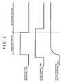
- Fig. 2is a timing chart illustrative of an operation sequence of the pixel circuit shown in Fig. 1 .
- the timing chartshows an operation sequence for sampling the potential of a video signal supplied from the signal line 1F (video signal line potential) and bringing the light-emitting device 1D, which may be an organic EL device, into a light-emitting state.
- the potential of the scanning line 1Escanning line potential
- the sampling transistor 1Ais turned on, charging the retention capacitor 1C with the video signal line potential.
- the gate potential Vg of the drive transistor 1Bstarts rising, and the drive transistor 1B starts to pass a drain current.
- the anode potential of the light-emitting device Dincreases, causing the light-emitting device D to start to emit light.
- the retention capacitor 1Cretains the video signal line potential, keeping the gate potential of the drive transistor 1B constant.
- the light emission luminance of the light-emitting device Dis kept constant until a next frame.
- the pixels of the display apparatussuffer threshold voltage and mobility variations due to fabrication process variations of the drive transistors 1B of the pixel circuits. Because of those characteristic variations, even when the same gate potential is applied to the drive transistors 1B of the pixel circuits, the pixels have their own drain current (drive current) variations, which will appear as light emission luminance variations. Furthermore, the light-emitting device 1D, which may be an organic EL device, has its characteristics varying with time, resulting in a variation of the anode potential of the light-emitting device 1D. The variation of the anode potential of the light-emitting device 1D causes a variation of the gate-to-source voltage of the drive transistor 1B, bringing about a variation of the drain current (drive current). The variations of the drive currents due to the various causes result in light emission luminance variations of the pixels, tending to degrade the displayed image quality.
- Fig. 3Ashows in block form an overall arrangement of a display apparatus according to an embodiment of the present invention.
- the display apparatusgenerally denoted by 100, includes a pixel array 102 and a driver 103, 104, 105.
- the pixel array 102has a plurality of scanning lines WSL101 through WSL10m provided as rows, a plurality of signal lines DTL101 through DTL10n provided as columns, a matrix of pixels (PXLC) 101 disposed at the respective intersections of the scanning lines WSL101 through WSL10m and the signal lines DTL101 through DTL10n, and a plurality of power supply lines DSL101 through DSL10m disposed along the respective rows of the pixels 101.
- PXLCmatrix of pixels
- the driverincludes a main scanner (write scanner WSCN) 104 for successively supplying control signals to the scanning lines WSL101 through WSL10m to perform line-sequential scanning on the rows of the pixels 101, a power supply scanner (DSCN) 105 for supplying a power supply voltage, which selectively switches between a first potential and a second potential, to the power supply lines DSL101 through DSL10m in synchronism with the line-sequential scanning, and a signal selector (horizontal selector (HSEL)) 103 for supplying a signal potential, which serves as a video signal, and a reference potential to the signal lines DTL101 through DTL10n as the columns in synchronism with the line-sequential scanning.
- a main scannerwrite scanner WSCN
- DSCNpower supply scanner
- DSCNpower supply scanner
- DSCNpower supply voltage
- HSELhorizontal selector
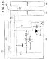
- Fig. 3Bis a circuit diagram showing specific structural details and interconnects of each of the pixels 101 of the display apparatus 100 shown in Fig. 3A .
- the pixel 101includes a light-emitting device 3D which may typically be an organic EL device, a sampling transistor 3A, a drive transistor 3B, and a retention capacitor 3C.
- the sampling transistor 3Ahas a gate connected to the corresponding scanning line WSL101. Either one of the source and drain of the sampling transistor 3A is connected to the corresponding signal line DTL101, and the other connected to the gate g of the drive transistor 3B.
- the drive transistor 3Bhas a source s and a drain d, either one of which is connected to the light-emitting device 3D, and the other connected to the corresponding power supply line DSL101.
- the drain d of the drive transistor 3Bis connected to the power supply line DSL101
- the source s of the drive transistor 3Bis connected to the anode of the light-emitting device 3D.
- the cathode of the light-emitting device 3Dis connected to a ground line 3H.
- the ground line 3His connected in common to all the pixels 101.
- the retention capacitor 3Cis connected between the source s and gate g of the drive transistor 3B.
- the sampling transistor 3Ais rendered conductive by a control signal supplied from the scanning line WSL101, samples a signal potential supplied from the signal line DTL101, and retains the sampled signal potential in the retention capacitor 3C.
- the drive transistor 3Bis supplied with a current from the power supply line DSL101 at the first potential, and passes a drive current to the light-emitting device 3D depending on the signal potential retained in the retention capacitor 3C.
- the power supply scanner (DSCN) 105switches the power supply line DSL101 from the first potential to the second potential, retaining a voltage which essentially corresponds to the threshold voltage Vth of the drive transistor 3B in the retention capacitor 3C.
- a threshold voltage correcting functionmakes allows the display apparatus 100 to cancel the effect of the threshold voltage of the drive transistor 3B which varies from pixel to pixel.
- the pixel 101 shown in Fig. 3Bhas a mobility correction function in addition to the above threshold voltage correcting function. Specifically, after the sampling transistor 3A is rendered conductive, the signal selector (HSEL) 103 switches the signal line DTL101 from the reference potential to the signal potential at a first timing, and the main scanner (WSCN) 104 stops applying the control signal to the scanning line WSL101 at a second timing after the first timing, thereby rendering the sampling transistor 3A nonconductive. The period between the first timing and the second timing is appropriately set to correct the signal potential as it is retained in the retention capacitor 3C is corrected with respect to the mobility ⁇ of the drive transistor 3B.
- the signal selector (HSEL) 103switches the signal line DTL101 from the reference potential to the signal potential at a first timing
- the main scanner (WSCN) 104stops applying the control signal to the scanning line WSL101 at a second timing after the first timing, thereby rendering the sampling transistor 3A nonconductive.
- the period between the first timing and the second timingis appropriately set to correct the
- the driver 103, 104, 105can adjust the relative phase difference between the video signal supplied by the signal selector 103 and the control signal supplied by the main scanner 104 for thereby optimizing the period between the first timing and the second timing (mobility correcting period).
- the signal selector 103can also apply a gradient to the positive-going edge of the video signal which switches from the reference potential to the signal potential for thereby allowing the mobility correcting period between the first timing and the second timing to automatically follow the signal potential.
- the pixel 101 shown in Fig. 3Balso has a bootstrap function. Specifically, at the time the signal potential is retained by the retention capacitor 3C, the main scanner (WSCN) 104 stops applying the control signal to the scanning line WSL101, thereby rendering the sampling transistor 3A nonconductive to electrically disconnect the gate g of the drive transistor 3B from the signal line DTL101. Therefore, the gate potential Vg is linked to a variation of the source potential Vs of the drive transistor 3B to keep constant the voltage Vgs between the gate g and the source s.
- Fig. 4Ais a timing chart illustrative of an operation sequence of the pixel 101 shown in Fig. 3B .
- Fig. 4Ashows potential changes of the scanning line WSL101, potential changes of the power supply line DSL101, and potential changes of the signal line DTL101 against a common time axis.
- Fig. 4Aalso shows changes in the gate potential Vg and the source potential Vs of the drive transistor 3B in addition to the above potential changes.
- the timing chart shown in Fig. 4Ais divided into different periods (B) through (G) of operation of the pixel 101.
- the light-emitting device 3Dis in a light-emitting state in a light-emitting period (B).
- a new field of line-sequential scanningbegins, and the gate potential Vg of the drive transistor 3B is initialized in a first period (C).
- the source potential Vs of the drive transistor 3Bis initialized.
- the pixel 101is fully prepared for its threshold voltage correcting operation.
- a threshold correcting periodE
- the threshold voltage correcting operationis actually performed to retain a voltage which essentially corresponds to the threshold voltage Vth between the gate g and the source s of the drive transistor 3B.
- the voltage corresponding to Vthis written in the retention capacitor 3C that is connected between the gate g and the source s of the drive transistor 3B.
- a sampling period/mobility correcting periodF
- the signal potential Vin of the video signalis rewritten in the retention capacitor 3C in addition to the threshold voltage Vth, and a voltage ⁇ V for correcting the mobility is subtracted from the voltage retained in the retention capacitor 3C.
- the light-emitting device 3Demits light at a luminance level depending on the signal voltage Vin. Since the signal voltage Vin has been adjusted by the voltage which essentially corresponds to the threshold voltage Vth and the mobility correcting voltage ⁇ V, the light emission luminance of the light-emitting device 3D is not adversely affected by the threshold voltage Vth and the mobility ⁇ of the drive transistor 3B.
- Figs. 4B through 4Gshow different operational stages which correspond respectively to the periods (B) through (G) of the timing chart shown in Fig. 4A .
- a capacitive component of the light-emitting device 3Dis illustrated as a capacitive element 31 in each of Figs. 4B through 4G .
- the power supply line DSL101is at a high potential Vcc_H (the first potential)
- the drive transistor 3Bsupplies a drive current Ids to the light-emitting device 3D.
- the drive current Idsflows from the power supply line DSL101 at the high potential Vcc_H through the drive transistor 3B and the light-emitting device 3D into the common ground line 3H.
- the scanning line WSL101goes high, turning on the sampling transistor 3A to initialize (reset) the gate potential Vg of the drive transistor 3B to the reference potential Vo of the video signal line DTL101.
- the power supply line DSL101switches from the high potential Vcc_H (the first potential) to a low potential Vcc_L (the second potential) which is sufficiently lower than the reference potential Vo of the video signal line DTL101.
- the source potential Vs of the drive transistor 3Bis initialized (reset) to the low potential Vcc_L which is sufficiently lower than the reference potential Vo of the video signal line DTL101.
- the low potential Vcc_L (the second potential) of the power supply line DSL101is established such that the gate-to-source voltage Vgs (the difference between the gate potential Vg and the source potential Vs) of the drive transistor 3B is greater than the threshold voltage Vth of the drive transistor 3B.
- threshold correcting period (E)the power supply line DSL101 switches from the low potential Vcc_L to the high potential Vcc_H, and the source potential Vs of the drive transistor 3B starts increasing.
- the gate-to-source voltage Vgs of the drive transistor 3Breaches the threshold voltage Vth, the current is cut off.
- the voltage which essentially corresponds to the threshold voltage Vth of the drive transistor 3Bis written in the retention capacitor 3C. This process is referred to as the threshold voltage correcting operation.
- the potential of the common ground line 3His set to cut off the light-emitting device 3D.
- the video signal line DTL101changes from the reference potential Vo to the signal potential Vin at the first timing, setting the gate potential Vg of the drive transistor 3B to Vin. Since the light-emitting device 3D is initially cut off (at a high impedance) at this time, the drain current Ids of the drive transistor 3B flows into the parasitic capacitance 3I of the light-emitting device 3D. The parasitic capacitance 3I of the light-emitting device 3D now starts being charged.
- the source potential Vs of the drive transistor 3Bstarts to increase, and the gate-to-source voltage Vgs of the drive transistor 3B reaches Vin + Vth - ⁇ V at the second timing.
- the signal potential Vinis sampled, and the correction variable ⁇ V is adjusted.
- Vinis higher, Ids is greater and the absolute value of ⁇ V is greater. Therefore, the mobility correction depending on the light emission luminance level can be performed. If Vin is constant, then the absolute value of ⁇ V is greater as the mobility ⁇ of the drive transistor 3B is greater. Stated otherwise, since the negative feedback variable ⁇ V is greater as the mobility ⁇ is greater, it is possible to remove variations of the mobility ⁇ for the respective pixels.
- the scanning line WSL101goes to the low potential, turning off the sampling transistor 3A.
- the gate g of the drive transistor 3Bis now separated from the signal line DTL101.
- the drain current Idsstarts flowing into the light-emitting device 3D.
- the anode potential of the light-emitting device 3Dincreases depending on the drive current Ids.
- the increase in the anode potential of the light-emitting device 3Dis equivalent to an increase in the source potential Vs of the drive transistor 3B.
- the gate potential Vg of the drive transistor 3Balso increases because of the bootstrapping operation of the retention capacitor 3C.
- the increased amount of the gate potential Vgis equal to the increased amount of the source potential Vs. Consequently, the gate-to-source voltage Vgs of the drive transistor 3B is maintained at the constant level of Vin + Vth - ⁇ V during the light-emitting period.
- Fig. 5is a graph showing current vs. voltage characteristics of the drive transistor 3B.
- the threshold voltage Vthvaries, the drain-to-source current Ids varies even if Vgs is constant.
- the gate-to-source voltage Vgsis expressed as Vin + Vth - ⁇ V when the pixel is emitting light
- drain-to-source current Idsdoes not vary, and hence the light emission luminance of the organic EL device does not vary.
- Fig. 6Ais also a graph showing current vs. voltage characteristics of different drive transistors.
- Fig. 6Ashows respective characteristic curves of two drive transistors having different mobilities ⁇ , ⁇ '. As can be seen from the characteristic curves shown in Fig. 6A , if the drive transistors have different mobilities ⁇ , ⁇ ', then they have different drain-to-source currents Ids, Ids' even when the gate voltage Vgs is constant.
- Fig. 6Bis a circuit diagram illustrative of the manner in which the pixel circuit shown in Fig. 3B operates for sampling the video signal potential and correcting the mobility.
- Fig. 6Balso illustrates the parasitic capacitance 3I of the light-emitting device 3D.
- the sampling transistor 3AFor sampling the video signal potential Vin, the sampling transistor 3A is turned on. Therefore, the gate potential Vg of the drive transistor 3B is set to the video signal potential Vin, and the gate-to-source voltage Vgs of the drive transistor 3B reaches Vin + Vth. At this time, the drive transistor 3B is turned on.
- the drain-to-source current Idsflows into the light-emitting device capacitance 3I.
- the drain-to-source current Idsflows into the light-emitting device capacitance 3I, the light-emitting device capacitance 3I starts being charged, causing the anode potential of the light-emitting device 3D (hence, the source potential Vs of the drive transistor 3B) to start increasing.
- the source potential Vs of the drive transistor 3Bincreases by ⁇ V
- the gate-to-source voltage Vgs of the drive transistor 3Bdecreases by ⁇ V. This process is referred to as the mobility correcting operation based on negative feedback.
- Fig. 6Cshows an operation timing sequence of the pixel circuit for determining the mobility correcting period t.
- a gradientis applied to the positive-going edge of the video signal potential for thereby allowing the mobility correcting period t to automatically follow the video signal potential, so that the mobility correcting period t is optimized.
- the mobility correcting period tis determined by the phase difference between the scanning line WSL101 and the video signal line DTL101, and also by the potential of the video signal line DTL101.
- the mobility correcting parameter ⁇ Vis greater as the drain-to-source current Ids of the drive transistor 3B is greater. Conversely, when the drain-to-source current Ids of the drive transistor 3B is smaller, the mobility correcting parameter ⁇ V is smaller. Therefore, the mobility correcting parameter ⁇ V is determined depending on the drain-to-source current Ids.
- the mobility correcting period tis not constant, but is adjusted depending on Ids. If Ids is greater, then the mobility correcting period t should be shorter, and if Ids is smaller, then the mobility correcting period t should be longer. In Fig.
- a gradientis applied to at least the positive-going edge of the video signal potential to automatically adjust the mobility correcting period t such that the mobility correcting period t is shorter when the potential of the video signal line DTL101 is higher (Ids is greater) and the mobility correcting period t is longer when the potential of the video signal line DTL101 is lower (Ids is smaller).
- Fig. 6Dis a graph illustrative of operating points of the drive transistor 3B at the time the mobility is corrected.
- optimum correcting parameters ⁇ V, ⁇ V'are determined to determine drain-to-source currents Ids, Ids' of the drive transistor 3B.
- the different mobilities ⁇ , ⁇ 'are given with respect to the gate-to-source voltage Vgs, then correspondingly different drain-to-source currents Ids0, Ids0' are produced.
- Fig. 7Ais a graph showing current vs. voltage characteristics of the light-emitting device 3D which is in the form of an organic EL device.
- the anode-to-cathode voltage Velis uniquely determined.
- the scanning line WS1101goes to the low potential, turning off the sampling transistor 3A, as shown in Fig. 4G , the anode potential of the light-emitting device 3D increases by the anode-to-cathode voltage Vel that is determined by the drain-to-source current Ids of the drive transistor 3B.
- Fig. 7Bis a graph showing potential variations of the gate potential Vg and the source potential Vs of the drive transistor 3B at the time the anode potential of the light-emitting device 3D increases.
- the source potential Vs of the drive transistor 3Bincreases by Vel
- the gate-to-source voltage of the drive transistor 3Bis kept at the constant level of Vin + Vth - ⁇ V at all times.
- Fig. 7Cis a circuit diagram of the pixel circuit shown in Fig. 3B , with parasitic capacitances 7A, 7B being illustrated.
- the parasitic capacitances 7A, 7Bare parasitically added to the gate g of the drive transistor 3B.
- the bootstrapping operation capability referred to aboveis expressed by Cs/(Cs + Cw + Cp) where Cs represents the capacitance value of the retention capacitor 3C and Cw, Cp the respective capacitance values of the parasitic capacitances 7A, 7B.
- Cs/(Cs + Cw + Cp)is closer to 1, the bootstrapping operation capability is higher, i.e., the correcting ability against the aging of the light-emitting device 3D is higher.
- the number of devices connected to the gate g of the drive transistor 3Bis held to a minimum. Therefore, the capacitance value Cp is negligible.
- the bootstrapping operation capabilitycan thus be expressed by Cs/(Cs + Cw) which is infinitely close to 1, indicating that the correcting ability against the aging of the light-emitting device 3D is high.
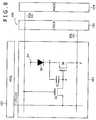
- Fig. 8is a circuit diagram of a pixel circuit of the display apparatus according to another embodiment of the present invention.
- the pixel circuit shown in Fig. 8is different from the pixel circuit shown in Fig. 3 in that whereas the pixel circuit shown in Fig. 3 employs N-type transistors, the pixel circuit shown in Fig. 8 employs P-type transistors.
- the pixel circuit shown in Fig. 8is capable of performing the threshold voltage correcting operation, the mobility correcting operation, and the bootstrapping operation exactly in the same manner as with the pixel circuit shown in Fig. 3 .
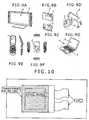
- the display apparatuscan be used as display apparatus for various electronic units as shown in Figs. 9A through 9G , including a digital camera, a notebook personal computer, a cellular phone unit, a video camera, etc., for displaying video signals generated in the electronic units as still images or video images.
- the display apparatusmay be of a module configuration as shown in Fig. 10 , such as a display module having a pixel matrix applied to a transparent facing unit.
- the display modulemay include a color filter, a protective film, and a light blocking film, etc. disposed on the transparent facing unit.
- the display modulemay also have FPCs (Flexible Printed Circuits) for inputting signals to and outputting signals from the pixel matrix.
- Fig. 9Ashows a television set having a video display screen 1 made up of a front panel 2, etc.
- the display apparatus according to an embodiment of the present inventionis incorporated in the video display screen 1.
- Figs. 9B and 9Cshow a digital camera including an image capturing lens 1, a flash light-emitting unit 2, a display unit 3, etc.
- the display apparatus according to an embodiment of the present inventionis incorporated in the display unit 3.
- Fig. 9Dshows a video camera including a main body 1, a display panel 2, etc.
- the display apparatus according to an embodiment of the present inventionis incorporated in the display panel 2.
- Figs. 9E and 9Fshow a cellular phone unit including a display panel 1, an auxiliary display panel 2, etc.
- the display apparatus according to an embodiment of the present inventionis incorporated in the display panel 1 and the auxiliary display panel 2.
- Fig. 9Gshows a notebook personal computer including a main body 1 having a keyboard 2 for entering characters, etc. and a display panel 3 for displaying images.
- the display apparatus according to an embodiment of the present inventionis incorporated in the display panel 3.
- the present inventioncontains subject matter related to Japanese Patent Application JP 2006-141836 filed in the Japan Patent Office on May 22, 2006.
- An embodiment of the present inventionprovides a display apparatus including a pixel array and a driver configured to drive the pixel array, the pixel array having scanning lines as rows, signal lines as columns, a matrix of pixels disposed at respective intersections of the scanning lines and the signal lines, and power supply lines disposed along respective rows of the pixels, the driver having a main scanner for successively supplying control signals to the scanning lines to perform line-sequential scanning on the rows of the pixels, a power supply scanner for supplying a power supply voltage, which selectively switches between a first potential and a second potential, to the power supply lines in synchronism with the line-sequential scanning, and a signal selector for supplying a signal potential, which serves as a video signal, and a reference potential to the signal lines as the columns in synchronism with the line-sequential scanning.
Landscapes
- Engineering & Computer Science (AREA)
- Physics & Mathematics (AREA)
- Computer Hardware Design (AREA)
- General Physics & Mathematics (AREA)
- Theoretical Computer Science (AREA)
- Control Of Indicators Other Than Cathode Ray Tubes (AREA)
- Control Of El Displays (AREA)
- Electroluminescent Light Sources (AREA)
- Liquid Crystal (AREA)
Description
- The present invention relates to a display apparatus such as an active-matrix display apparatus having light-emitting devices as pixels thereof, and a method of driving such a display apparatus.
- In recent years, growing efforts have been made to develop flat self-emission display apparatus using organic EL devices as light-emitting devices. An organic EL device is a device utilizing a phenomenon in which an organic thin film emits light under an electric field. The organic EL device has a low power requirement because it can be energized under a low voltage of 10 V or lower. Since the organic EL device is a self-emission device for emitting light by itself, it requires no illuminating members, and hence can be lightweight and of a low profile. The organic EL device does not produce an image lag when it displays moving images because the response speed thereof is of a very high value of about several µs.
- Of flat self-emission display apparatus using organic EL devices as pixels, active-matrix display apparatus including thin-film transistors integrated in respective pixels as drive elements are particularly under active development. Active-matrix flat self-emission display apparatus are disclosed in Japanese laid-open patent publication Nos.
2003-255856 2003-271095 2004-133240 2004-029791 2004-093682 - In the existing active-matrix flat self-emission display apparatus, transistors for driving light-emitting devices have various threshold voltages and mobilities due to fabrication process variations. In addition, the characteristics of the organic EL devices tend to vary with time. Such characteristic variations of the drive transistors and characteristic variations of the organic EL devices adversely affect the light emission luminance. For uniformly controlling the light emission luminance over the entire screen surface of the display apparatus, it is necessary to correct the above characteristic variations of the drive transistors and the organic EL devices in pixel circuits. There have heretofore been proposed display apparatus having a correcting function at each pixel. However, existing pixel circuits with a correcting function are complex in structure as they demand an interconnect for supplying a correcting potential, a switching transistor, and a switching pulse. Because each of the pixel circuits has many components, they have presented obstacles to efforts to achieve higher-definition display.
US 2005/0206590 describes an image display apparatus that comprises a pixel having a drive transistor and a pixel display element which are connected in series between a first power line and a second power line, a holding capacitor connected to a gate electrode of the drive transistor, and a selection transistor connected between a signal line and the gate electrode of the drive transistor. When the selection transistor is turned on, gradation pixel data is written in the holding capacitor from the signal line. The charge of gradation pixel data written in the holding capacitor is discharged for a certain period through the drive transistor, thereafter the charge of the gradation pixel data stored in the holding capacitor is held by floating the gate electrode of the drive transistor.- It is desirable to provide a display apparatus for achieving higher-definition display with simplified pixel circuits, and a method of driving such a display apparatus.
- Particular and preferred aspects of the present invention are set out in the accompanying independent and dependent claims.
- The display apparatus according to an embodiment of the present invention has a threshold voltage correcting function, a mobility correcting function, and a bootstrapping function in each of the pixels. The threshold voltage correcting function corrects a variation of the threshold voltage of the drivetransistor. The mobility correcting function corrects a variation of the mobility of the drive transistor. Bootstrapping operation of the retention capacitor at the time the light-emitting device emits light is effective to keep the light emission luminance at a constant level at all times regardless of characteristic variations of an organic EL device used as the light-emitting device. Specifically, even if the current vs. voltage characteristics of the organic EL device vary with time, since the gate-to-source voltage of the drive transistor is kept constant by the retention capacitor that is bootstrapped, the light emission luminance is maintained at a constant level.
- In order to incorporate the threshold voltage correcting function, the mobility correcting function, and the bootstrapping function into each of the pixels, the power supply voltage supplied to each of the pixels is applied as switching pulses. With the power supply voltage applied as switching pulses, a switching transistor for correcting the threshold voltage and a scanning line for controlling the gate of the switching transistor are not demanded. As a result, the number of components and interconnects of the pixel is greatly reduced, making it possible to reduce the pixel area for providing higher-definition display. The mobility correcting period can be adjusted based on the phase difference between the video signal and the sampling pulse by correcting the mobility simultaneously with the sampling of the video signal potential. Furthermore, the mobility correcting period can be controlled to automatically follow the level of the video signal. Because the number of components of the pixel is small, any parasitic capacitance added to the gate of the drive transistor is small, so that the retention capacitor can reliably be bootstrapped for thereby improving the ability to correct a time-depending variation of the organic EL device.
- According to an embodiment of the present invention, an active-matrix display apparatus is provided employing light-emitting devices such as organic EL devices as pixels, each of the pixels having a threshold voltage correcting function for the drive transistor, a mobility correcting function for the drive transistor, and a function to correct a time-depending variation of the organic EL device (bootstrapping function) for allowing the display apparatus to display high-quality images. Since the mobility correcting period can automatically be set depending on the video signal potential, the mobility can be corrected regardless of the luminance and pattern of displayed images. An existing pixel circuit with such correcting functions is made of a large number of components, has a large layout area, and hence is not suitable for providing higher-definition display. According to an embodiment of the present invention, however, since the power supply voltage is applied as switching pulses, the number of components and interconnects of the pixel is greatly reduced, making it possible to reduce the pixel layout area. Consequently, the display apparatus according to an embodiment of the present invention can be provided as a high-quality, high-definition flat display unit.
- Further particular and preferred aspects of the present invention are set out in the accompanying independent and dependent claims. Features of the dependent claims may be combined with features of the independent claims as appropriate, and in combinations other than those explicitly set out in the claims.
- The present invention will be described further, by way of example only, with reference to preferred embodiments thereof as illustrated in the accompanying drawings, in which:
Fig. 1 is a circuit diagram of a general pixel structure;Fig. 2 is a timing chart illustrative of an operation sequence of the pixel circuit shown inFig. 1 ;Fig. 3A is a block diagram of an overall arrangement of a display apparatus according to an embodiment of the present invention;Fig. 3B is a circuit diagram of a pixel circuit of the display apparatus according to an embodiment of the present invention;Fig. 4A is a timing chart illustrative of an operation sequence of the pixel circuit shown inFig. 3B ;Fig. 4B is a circuit diagram illustrative of the manner in which the pixel circuit shown inFig. 3B operates;Fig. 4C is a circuit diagram illustrative of the manner in which the pixel circuit shown inFig. 3B operates;Fig. 4D is a circuit diagram illustrative of the manner in which the pixel circuit shown inFig. 3B operates;Fig. 4E is a circuit diagram illustrative of the manner in which the pixel circuit shown inFig. 3B operates;Fig. 4F is a circuit diagram illustrative of the manner in which the pixel circuit shown inFig. 3B operates;Fig. 4G is a circuit diagram illustrative of the manner in which the pixel circuit shown inFig. 3B operates;Fig. 5 is a graph showing current vs. voltage characteristics of a drive transistor;Fig. 6A is a graph showing current vs. voltage characteristics of different drive transistors;Fig. 6B is a circuit diagram illustrative of the manner in which the pixel circuit shown inFig. 3B operates;Fig. 6C is a waveform diagram illustrative of the manner in which the pixel circuit shown inFig. 3B operates;Fig. 6D is a graph showing current vs. voltage characteristics, which is illustrative of the manner in which the pixel circuit shown inFig. 3B operates;Fig. 7A is a graph showing current vs. voltage characteristics of a light-emitting device;Fig. 7B is a waveform diagram showing a bootstrap operation of the drive transistor;Fig. 7C is a circuit diagram illustrative of the manner in which the pixel circuit shown inFig. 3B operates;Fig. 8 is a circuit diagram of a pixel circuit of the display apparatus according to another embodiment of the present invention;Figs. 9(a) through 9(g) are views showing specific examples of electronic unit display apparatus; andFig. 10 is a plan view of a module.- For an easier understanding of the present invention and a clarification of the background thereof, a general structure of a display apparatus will initially be described below with reference to
Fig. 1. Fig. 1 is a circuit diagram showing a pixel of a general display apparatus. As shown inFig. 1 , the pixel circuit has a sampling transistor 1A disposed at the intersection of ascanning line 1E and asignal line 1F which extend perpendicularly to each other. The sampling transistor 1A is an N-type transistor having a gate connected to thescanning line 1E and a drain connected to thesignal line 1F. The sampling transistor 1A has a source connected to an electrode of aretention capacitor 1C and the gate of adrive transistor 1B. Thedrive transistor 1B is an N-type transistor having a drain connected to apower supply line 1G and a source connected to the anode of a light-emittingdevice 1D. The other electrode of theretention capacitor 1C and the cathode of the light-emittingdevice 1D are connected to aground line 1H. Fig. 2 is a timing chart illustrative of an operation sequence of the pixel circuit shown inFig. 1 . The timing chart shows an operation sequence for sampling the potential of a video signal supplied from thesignal line 1F (video signal line potential) and bringing the light-emittingdevice 1D, which may be an organic EL device, into a light-emitting state. When the potential of thescanning line 1E (scanning line potential) goes high, the sampling transistor 1A is turned on, charging theretention capacitor 1C with the video signal line potential. The gate potential Vg of thedrive transistor 1B starts rising, and thedrive transistor 1B starts to pass a drain current. Therefore, the anode potential of the light-emitting device D increases, causing the light-emitting device D to start to emit light. When the scanning line potential goes low, theretention capacitor 1C retains the video signal line potential, keeping the gate potential of thedrive transistor 1B constant. The light emission luminance of the light-emitting device D is kept constant until a next frame.- The pixels of the display apparatus suffer threshold voltage and mobility variations due to fabrication process variations of the
drive transistors 1B of the pixel circuits. Because of those characteristic variations, even when the same gate potential is applied to thedrive transistors 1B of the pixel circuits, the pixels have their own drain current (drive current) variations, which will appear as light emission luminance variations. Furthermore, the light-emittingdevice 1D, which may be an organic EL device, has its characteristics varying with time, resulting in a variation of the anode potential of the light-emittingdevice 1D. The variation of the anode potential of the light-emittingdevice 1D causes a variation of the gate-to-source voltage of thedrive transistor 1B, bringing about a variation of the drain current (drive current). The variations of the drive currents due to the various causes result in light emission luminance variations of the pixels, tending to degrade the displayed image quality. Fig. 3A shows in block form an overall arrangement of a display apparatus according to an embodiment of the present invention. As shown inFig. 3A , the display apparatus, generally denoted by 100, includes apixel array 102 and adriver pixel array 102 has a plurality of scanning lines WSL101 through WSL10m provided as rows, a plurality of signal lines DTL101 through DTL10n provided as columns, a matrix of pixels (PXLC) 101 disposed at the respective intersections of the scanning lines WSL101 through WSL10m and the signal lines DTL101 through DTL10n, and a plurality of power supply lines DSL101 through DSL10m disposed along the respective rows of thepixels 101. The driver includes a main scanner (write scanner WSCN) 104 for successively supplying control signals to the scanning lines WSL101 through WSL10m to perform line-sequential scanning on the rows of thepixels 101, a power supply scanner (DSCN) 105 for supplying a power supply voltage, which selectively switches between a first potential and a second potential, to the power supply lines DSL101 through DSL10m in synchronism with the line-sequential scanning, and a signal selector (horizontal selector (HSEL)) 103 for supplying a signal potential, which serves as a video signal, and a reference potential to the signal lines DTL101 through DTL10n as the columns in synchronism with the line-sequential scanning.Fig. 3B is a circuit diagram showing specific structural details and interconnects of each of thepixels 101 of thedisplay apparatus 100 shown inFig. 3A . As shown inFig. 3B , thepixel 101 includes a light-emittingdevice 3D which may typically be an organic EL device, asampling transistor 3A, adrive transistor 3B, and aretention capacitor 3C. Thesampling transistor 3A has a gate connected to the corresponding scanning line WSL101. Either one of the source and drain of thesampling transistor 3A is connected to the corresponding signal line DTL101, and the other connected to the gate g of thedrive transistor 3B. Thedrive transistor 3B has a source s and a drain d, either one of which is connected to the light-emittingdevice 3D, and the other connected to the corresponding power supply line DSL101. In the present embodiment, the drain d of thedrive transistor 3B is connected to the power supply line DSL101, and the source s of thedrive transistor 3B is connected to the anode of the light-emittingdevice 3D. The cathode of the light-emittingdevice 3D is connected to aground line 3H. Theground line 3H is connected in common to all thepixels 101. Theretention capacitor 3C is connected between the source s and gate g of thedrive transistor 3B.- The
sampling transistor 3A is rendered conductive by a control signal supplied from the scanning line WSL101, samples a signal potential supplied from the signal line DTL101, and retains the sampled signal potential in theretention capacitor 3C. Thedrive transistor 3B is supplied with a current from the power supply line DSL101 at the first potential, and passes a drive current to the light-emittingdevice 3D depending on the signal potential retained in theretention capacitor 3C. After thesampling transistor 3A is rendered conductive, while the signal selector (HSEL) 103 is supplying the reference potential to the signal line DTL101, the power supply scanner (DSCN) 105 switches the power supply line DSL101 from the first potential to the second potential, retaining a voltage which essentially corresponds to the threshold voltage Vth of thedrive transistor 3B in theretention capacitor 3C. Such a threshold voltage correcting function makes allows thedisplay apparatus 100 to cancel the effect of the threshold voltage of thedrive transistor 3B which varies from pixel to pixel. - The
pixel 101 shown inFig. 3B has a mobility correction function in addition to the above threshold voltage correcting function. Specifically, after thesampling transistor 3A is rendered conductive, the signal selector (HSEL) 103 switches the signal line DTL101 from the reference potential to the signal potential at a first timing, and the main scanner (WSCN) 104 stops applying the control signal to the scanning line WSL101 at a second timing after the first timing, thereby rendering thesampling transistor 3A nonconductive. The period between the first timing and the second timing is appropriately set to correct the signal potential as it is retained in theretention capacitor 3C is corrected with respect to the mobility µ of thedrive transistor 3B. Thedriver signal selector 103 and the control signal supplied by themain scanner 104 for thereby optimizing the period between the first timing and the second timing (mobility correcting period). Thesignal selector 103 can also apply a gradient to the positive-going edge of the video signal which switches from the reference potential to the signal potential for thereby allowing the mobility correcting period between the first timing and the second timing to automatically follow the signal potential. - The
pixel 101 shown inFig. 3B also has a bootstrap function. Specifically, at the time the signal potential is retained by theretention capacitor 3C, the main scanner (WSCN) 104 stops applying the control signal to the scanning line WSL101, thereby rendering thesampling transistor 3A nonconductive to electrically disconnect the gate g of thedrive transistor 3B from the signal line DTL101. Therefore, the gate potential Vg is linked to a variation of the source potential Vs of thedrive transistor 3B to keep constant the voltage Vgs between the gate g and the source s. Fig. 4A is a timing chart illustrative of an operation sequence of thepixel 101 shown inFig. 3B .Fig. 4A shows potential changes of the scanning line WSL101, potential changes of the power supply line DSL101, and potential changes of the signal line DTL101 against a common time axis.Fig. 4A also shows changes in the gate potential Vg and the source potential Vs of thedrive transistor 3B in addition to the above potential changes.- The timing chart shown in
Fig. 4A is divided into different periods (B) through (G) of operation of thepixel 101. Specifically, the light-emittingdevice 3D is in a light-emitting state in a light-emitting period (B). Thereafter, a new field of line-sequential scanning begins, and the gate potential Vg of thedrive transistor 3B is initialized in a first period (C). Then, in a next period (D), the source potential Vs of thedrive transistor 3B is initialized. When the gate potential Vg and the source potential Vs of thedrive transistor 3B are initialized, thepixel 101 is fully prepared for its threshold voltage correcting operation. In a threshold correcting period (E), the threshold voltage correcting operation is actually performed to retain a voltage which essentially corresponds to the threshold voltage Vth between the gate g and the source s of thedrive transistor 3B. In reality, the voltage corresponding to Vth is written in theretention capacitor 3C that is connected between the gate g and the source s of thedrive transistor 3B. Then, in a sampling period/mobility correcting period (F), the signal potential Vin of the video signal is rewritten in theretention capacitor 3C in addition to the threshold voltage Vth, and a voltage ΔV for correcting the mobility is subtracted from the voltage retained in theretention capacitor 3C. Thereafter, in a light-emitting period (G), the light-emittingdevice 3D emits light at a luminance level depending on the signal voltage Vin. Since the signal voltage Vin has been adjusted by the voltage which essentially corresponds to the threshold voltage Vth and the mobility correcting voltage ΔV, the light emission luminance of the light-emittingdevice 3D is not adversely affected by the threshold voltage Vth and the mobility µ of thedrive transistor 3B. A bootstrap operation is performed in an initial phase of the light-emitting period (G) to increase the gate potential Vg and the source potential Vs of thedrive transistor 3B while keeping constant the gate-to-source voltage Vgs = Vin + Vth - ΔV of thedrive transistor 3B. - Operation of the
pixel 101 shown inFig. 3B will be described in detail below with reference toFigs. 4B through 4G. Figs. 4B through 4G show different operational stages which correspond respectively to the periods (B) through (G) of the timing chart shown inFig. 4A . For an easier understanding of embodiments of the invention, a capacitive component of the light-emittingdevice 3D is illustrated as acapacitive element 31 in each ofFigs. 4B through 4G . As shown inFig. 4B , in the light-emitting period (B), the power supply line DSL101 is at a high potential Vcc_H (the first potential), and thedrive transistor 3B supplies a drive current Ids to the light-emittingdevice 3D. The drive current Ids flows from the power supply line DSL101 at the high potential Vcc_H through thedrive transistor 3B and the light-emittingdevice 3D into thecommon ground line 3H. - In the period (C), as shown in
Fig. 4C , the scanning line WSL101 goes high, turning on thesampling transistor 3A to initialize (reset) the gate potential Vg of thedrive transistor 3B to the reference potential Vo of the video signal line DTL101. - In the period (D), as shown in
Fig. 4D , the power supply line DSL101 switches from the high potential Vcc_H (the first potential) to a low potential Vcc_L (the second potential) which is sufficiently lower than the reference potential Vo of the video signal line DTL101. The source potential Vs of thedrive transistor 3B is initialized (reset) to the low potential Vcc_L which is sufficiently lower than the reference potential Vo of the video signal line DTL101. Specifically, the low potential Vcc_L (the second potential) of the power supply line DSL101 is established such that the gate-to-source voltage Vgs (the difference between the gate potential Vg and the source potential Vs) of thedrive transistor 3B is greater than the threshold voltage Vth of thedrive transistor 3B. - In threshold correcting period (E), as shown in
Fig. 4(E) , the power supply line DSL101 switches from the low potential Vcc_L to the high potential Vcc_H, and the source potential Vs of thedrive transistor 3B starts increasing. When the gate-to-source voltage Vgs of thedrive transistor 3B reaches the threshold voltage Vth, the current is cut off. In this manner, the voltage which essentially corresponds to the threshold voltage Vth of thedrive transistor 3B is written in theretention capacitor 3C. This process is referred to as the threshold voltage correcting operation. In order to cause the current to flow only into theretention capacitor 3C, but not to the light-emittingdevice 3D, the potential of thecommon ground line 3H is set to cut off the light-emittingdevice 3D. - In the sampling period/mobility correcting period (F), as shown in
Fig. 4F , the video signal line DTL101 changes from the reference potential Vo to the signal potential Vin at the first timing, setting the gate potential Vg of thedrive transistor 3B to Vin. Since the light-emittingdevice 3D is initially cut off (at a high impedance) at this time, the drain current Ids of thedrive transistor 3B flows into the parasitic capacitance 3I of the light-emittingdevice 3D. The parasitic capacitance 3I of the light-emittingdevice 3D now starts being charged. Therefore, the source potential Vs of thedrive transistor 3B starts to increase, and the gate-to-source voltage Vgs of thedrive transistor 3B reaches Vin + Vth - ΔV at the second timing. In this manner, the signal potential Vin is sampled, and the correction variable ΔV is adjusted. As Vin is higher, Ids is greater and the absolute value of ΔV is greater. Therefore, the mobility correction depending on the light emission luminance level can be performed. If Vin is constant, then the absolute value of ΔV is greater as the mobility µ of thedrive transistor 3B is greater. Stated otherwise, since the negative feedback variable ΔV is greater as the mobility µ is greater, it is possible to remove variations of the mobility µ for the respective pixels. - Finally in the light-emitting period (G), as shown in
Fig. 4G , the scanning line WSL101 goes to the low potential, turning off thesampling transistor 3A. The gate g of thedrive transistor 3B is now separated from the signal line DTL101. At the same time, the drain current Ids starts flowing into the light-emittingdevice 3D. The anode potential of the light-emittingdevice 3D increases depending on the drive current Ids. The increase in the anode potential of the light-emittingdevice 3D is equivalent to an increase in the source potential Vs of thedrive transistor 3B. As the source potential Vs of thedrive transistor 3B, the gate potential Vg of thedrive transistor 3B also increases because of the bootstrapping operation of theretention capacitor 3C. The increased amount of the gate potential Vg is equal to the increased amount of the source potential Vs. Consequently, the gate-to-source voltage Vgs of thedrive transistor 3B is maintained at the constant level of Vin + Vth - ΔV during the light-emitting period. Fig. 5 is a graph showing current vs. voltage characteristics of thedrive transistor 3B. The drain-to-source current Ids of thedrive transistor 3B while it is operating in a saturated region is expressed as Ids = (1/2)·µ·(W/L)·Cox·(Vgs - Vth)2 where µ represents the mobility, W the gate width, L the gate length, and Cox the gate oxide film capacitance per unit area. As can be seen from this transistor characteristic equation, when the threshold voltage Vth varies, the drain-to-source current Ids varies even if Vgs is constant. Since the gate-to-source voltage Vgs is expressed as Vin + Vth - ΔV when the pixel is emitting light, if Vgs = Vin + Vth - ΔV is substituted in the above transistor characteristic equation, then the drain-to-source current Ids is expressed as Ids = (1/2)·µ·(W/L)·Cox·(Vin - ΔV)2, and does no depend on the threshold voltage Vth. As a result, even if the threshold voltage Vth varies due to the fabrication process, drain-to-source current Ids does not vary, and hence the light emission luminance of the organic EL device does not vary.- If no countermeasure is taken, then, as shown in
Fig. 5 , the drive current corresponding to the gate voltage Vgs at the time the threshold voltage is Vth is indicated by Ids, whereas the drive current corresponding to the same gate voltage Vgs when the threshold voltage is Vth' is indicated by Ids' which is different from Ids. Fig. 6A is also a graph showing current vs. voltage characteristics of different drive transistors.Fig. 6A shows respective characteristic curves of two drive transistors having different mobilities µ, µ'. As can be seen from the characteristic curves shown inFig. 6A , if the drive transistors have different mobilities µ, µ', then they have different drain-to-source currents Ids, Ids' even when the gate voltage Vgs is constant.Fig. 6B is a circuit diagram illustrative of the manner in which the pixel circuit shown inFig. 3B operates for sampling the video signal potential and correcting the mobility. For an easier understanding of embodiments of the invention,Fig. 6B also illustrates the parasitic capacitance 3I of the light-emittingdevice 3D. For sampling the video signal potential Vin, thesampling transistor 3A is turned on. Therefore, the gate potential Vg of thedrive transistor 3B is set to the video signal potential Vin, and the gate-to-source voltage Vgs of thedrive transistor 3B reaches Vin + Vth. At this time, thedrive transistor 3B is turned on. As the light-emittingdevice 3D is cut off, the drain-to-source current Ids flows into the light-emitting device capacitance 3I. When the drain-to-source current Ids flows into the light-emitting device capacitance 3I, the light-emitting device capacitance 3I starts being charged, causing the anode potential of the light-emittingdevice 3D (hence, the source potential Vs of thedrive transistor 3B) to start increasing. When the source potential Vs of thedrive transistor 3B increases by ΔV, the gate-to-source voltage Vgs of thedrive transistor 3B decreases by ΔV. This process is referred to as the mobility correcting operation based on negative feedback. The reduced amount ΔV of the gate-to-source voltage Vgs is determined by ΔV = Ids·Cel/t and serves as a parameter for the mobility correction, where Cel represents the capacitance value of the light-emitting device capacitance 3I and t the mobility correcting period, i.e., the period between the first timing and the second timing.Fig. 6C shows an operation timing sequence of the pixel circuit for determining the mobility correcting period t. InFig. 6C , a gradient is applied to the positive-going edge of the video signal potential for thereby allowing the mobility correcting period t to automatically follow the video signal potential, so that the mobility correcting period t is optimized. As shown inFig. 6C , the mobility correcting period t is determined by the phase difference between the scanning line WSL101 and the video signal line DTL101, and also by the potential of the video signal line DTL101. The mobility correcting parameter ΔV is represented by ΔV = Ids·cel/t. As can be seen from this equation, the mobility correcting parameter ΔV is greater as the drain-to-source current Ids of thedrive transistor 3B is greater. Conversely, when the drain-to-source current Ids of thedrive transistor 3B is smaller, the mobility correcting parameter ΔV is smaller. Therefore, the mobility correcting parameter ΔV is determined depending on the drain-to-source current Ids. The mobility correcting period t is not constant, but is adjusted depending on Ids. If Ids is greater, then the mobility correcting period t should be shorter, and if Ids is smaller, then the mobility correcting period t should be longer. InFig. 6C , a gradient is applied to at least the positive-going edge of the video signal potential to automatically adjust the mobility correcting period t such that the mobility correcting period t is shorter when the potential of the video signal line DTL101 is higher (Ids is greater) and the mobility correcting period t is longer when the potential of the video signal line DTL101 is lower (Ids is smaller).Fig. 6D is a graph illustrative of operating points of thedrive transistor 3B at the time the mobility is corrected. When the above mobility correction is performed on the different mobilities µ, p' due to the fabrication process, optimum correcting parameters ΔV, ΔV' are determined to determine drain-to-source currents Ids, Ids' of thedrive transistor 3B. In the absence of the mobility correction, if the different mobilities µ, µ' are given with respect to the gate-to-source voltage Vgs, then correspondingly different drain-to-source currents Ids0, Ids0' are produced. To solve the above problem, appropriate correcting parameters ΔV, ΔV' are applied respectively to the different mobilities µ, µ' to determine drain-to-source currents Ids, Ids' at the same level. A review of the graph shown inFig. 6D clearly indicates that negative feedback is applied to make the correcting variable ΔV greater when the mobility µ is greater and also to make correcting variable ΔV' smaller when the mobility µ' is smaller.Fig. 7A is a graph showing current vs. voltage characteristics of the light-emittingdevice 3D which is in the form of an organic EL device. When a current Iel starts to flow into the light-emittingdevice 3D, the anode-to-cathode voltage Vel is uniquely determined. When the scanning line WS1101 goes to the low potential, turning off thesampling transistor 3A, as shown inFig. 4G , the anode potential of the light-emittingdevice 3D increases by the anode-to-cathode voltage Vel that is determined by the drain-to-source current Ids of thedrive transistor 3B.Fig. 7B is a graph showing potential variations of the gate potential Vg and the source potential Vs of thedrive transistor 3B at the time the anode potential of the light-emittingdevice 3D increases. When the anode potential of the light-emittingdevice 3D increases by Vel, the source potential Vs of thedrive transistor 3B also increases by Vel, and the gate potential Vg of thedrive transistor 3B also increases by Vel due to the bootstrapping operation of theretention capacitor 3C. Therefore, the gate-to-source voltage Vgs = Vin + Vth - ΔV of thedrive transistor 3, which is retained before the bootstrapping operation, is also retained after the bootstrapping operation. Even if the anode potential of the light-emittingdevice 3D varies due to aging of the light-emittingdevice 3D, the gate-to-source voltage of thedrive transistor 3B is kept at the constant level of Vin + Vth - ΔV at all times.Fig. 7C is a circuit diagram of the pixel circuit shown inFig. 3B , withparasitic capacitances parasitic capacitances drive transistor 3B. The bootstrapping operation capability referred to above is expressed by Cs/(Cs + Cw + Cp) where Cs represents the capacitance value of theretention capacitor 3C and Cw, Cp the respective capacitance values of theparasitic capacitances device 3D is higher. According to an embodiment of the present invention, the number of devices connected to the gate g of thedrive transistor 3B is held to a minimum. Therefore, the capacitance value Cp is negligible. The bootstrapping operation capability can thus be expressed by Cs/(Cs + Cw) which is infinitely close to 1, indicating that the correcting ability against the aging of the light-emittingdevice 3D is high.Fig. 8 is a circuit diagram of a pixel circuit of the display apparatus according to another embodiment of the present invention. For an easier understanding of this embodiment of the invention, those parts shown inFig. 8 which correspond to those shown inFig. 3B are denoted by corresponding reference characters. The pixel circuit shown inFig. 8 is different from the pixel circuit shown inFig. 3 in that whereas the pixel circuit shown inFig. 3 employs N-type transistors, the pixel circuit shown inFig. 8 employs P-type transistors. The pixel circuit shown inFig. 8 is capable of performing the threshold voltage correcting operation, the mobility correcting operation, and the bootstrapping operation exactly in the same manner as with the pixel circuit shown inFig. 3 .- The display apparatus according to an embodiment of the present invention as described above can be used as display apparatus for various electronic units as shown in
Figs. 9A through 9G , including a digital camera, a notebook personal computer, a cellular phone unit, a video camera, etc., for displaying video signals generated in the electronic units as still images or video images. - The display apparatus according to an embodiment of the present invention may be of a module configuration as shown in
Fig. 10 , such as a display module having a pixel matrix applied to a transparent facing unit. The display module may include a color filter, a protective film, and a light blocking film, etc. disposed on the transparent facing unit. The display module may also have FPCs (Flexible Printed Circuits) for inputting signals to and outputting signals from the pixel matrix. - The electronic units as shown in
Figs. 9A through 9G will be described below. Fig. 9A shows a television set having avideo display screen 1 made up of afront panel 2, etc. The display apparatus according to an embodiment of the present invention is incorporated in thevideo display screen 1.Figs. 9B and 9C show a digital camera including animage capturing lens 1, a flash light-emittingunit 2, adisplay unit 3, etc. The display apparatus according to an embodiment of the present invention is incorporated in thedisplay unit 3.Fig. 9D shows a video camera including amain body 1, adisplay panel 2, etc. The display apparatus according to an embodiment of the present invention is incorporated in thedisplay panel 2.Figs. 9E and 9F show a cellular phone unit including adisplay panel 1, anauxiliary display panel 2, etc. The display apparatus according to an embodiment of the present invention is incorporated in thedisplay panel 1 and theauxiliary display panel 2.Fig. 9G shows a notebook personal computer including amain body 1 having akeyboard 2 for entering characters, etc. and adisplay panel 3 for displaying images. The display apparatus according to an embodiment of the present invention is incorporated in thedisplay panel 3.- The present invention contains subject matter related to Japanese Patent Application
JP 2006-141836 - An embodiment of the present invention provides a display apparatus including a pixel array and a driver configured to drive the pixel array, the pixel array having scanning lines as rows, signal lines as columns, a matrix of pixels disposed at respective intersections of the scanning lines and the signal lines, and power supply lines disposed along respective rows of the pixels, the driver having a main scanner for successively supplying control signals to the scanning lines to perform line-sequential scanning on the rows of the pixels, a power supply scanner for supplying a power supply voltage, which selectively switches between a first potential and a second potential, to the power supply lines in synchronism with the line-sequential scanning, and a signal selector for supplying a signal potential, which serves as a video signal, and a reference potential to the signal lines as the columns in synchronism with the line-sequential scanning.
- In so far as the embodiments of the invention described above are implemented, at least in part, using software-controlled data processing apparatus, it will be appreciated that a computer program providing such software control and a transmission, storage or other medium by which such a computer program is provided are envisaged as aspects of the present invention.
- Although particular embodiments have been described herein, it will be appreciated that the invention is not limited thereto and that many modifications and additions thereto may be made within the scope of the invention. For example, various combinations of the features of the following dependent claims can be made with the features of the independent claims without departing from the scope of the present invention.
Claims (5)
- A display apparatus comprising
a pixel array (102) and a driver (103, 104, 105) configured to drive the pixel array,
said pixel array having scanning lines (WSL101 ... WSL10m) as rows, signal lines (DTL101 ... DTL10n) as columns, a matrix of pixels (101) disposed at respective intersections of said scanning lines and said signal lines, and power supply lines (DSL101 ... DSL10m) disposed along respective rows of said pixels,
said driver having a main scanner (104) configured to supply control signals to said scanning lines, a power supply scanner (105) configured to supply a first potential (Vcc_H) and a second potential (Vcc_L) to said power supply lines, and a signal selector (103) configured to supply a signal potential (Vin), which serves as a video signal, and a reference potential (Vo) to said signal lines,
each of said pixels including a light-emitting device (3D), a sampling transistor (3A), a drive transistor (3B), and a retention capacitor (3C),
said sampling transistor (3A) having a gate, a source, and a drain, said gate being connected to one of said scanning lines, either one of said source and said drain being connected to one of said signal lines, and the other of said source and said drain being connected to the gate of said drive transistor,
said drive transistor (3B) having a source and a drain, either one of which is connected to said light-emitting device and the other connected to one of said power supply lines,
said retention capacitor (3C) having one end connected to the gate of said drive transistor and having its other end connected to the one of said source and said drain of the drive transistor connected to said light-emitting device,
wherein the main scanner (104) is arranged to render said sampling transistor conductive by supplying a control signal to the associated one of said scanning lines,
said power supply scanner (105) is arranged, after the sampling transistor has been rendered conductive by supplying the control signal to the associated one of said scanning lines and following an initialization period (C) in which the signal selector is controlled to supply the reference potential (Vo) to the associated one of said signal lines so that the gate potential of the drive transistor is reset to the reference potential (Vo), to perform a first switch to switch the power supply line from said first potential to said second potential and subsequently to perform a second switch to switch the power supply line from said second potential back to said first potential;
said signal selector is arranged to supply the reference potential to said signal line throughout the period between said first switch and said second switch, the second potential being lower than the reference potential by at least the threshold voltage of the drive transistor;
after the second switch, during a threshold correcting period (E) the power supply line is maintained at said first potential, and the signal line is maintained at said reference potential to enable the one of the source and the drain of the drive transistor connected to said light-emitting device to reach a potential such that a voltage which essentially corresponds to the threshold voltage of said drive transistor is retained in said retention capacitor; and
said signal selector being controlled, after the threshold correcting period, to switch said signal line from the reference potential to the signal potential;
wherein the signal selector is configured to switch the signal line from the reference potential to the signal potential at a first timing after the sampling transistor is rendered conductive, the main scanner is configured to stop applying the control signal to the scanning line at a second timing after the first timing, thereby rendering the sampling transistor nonconductive, and the period between the first timing and the second timing is appropriately set to correct the signal potential as it is retained in the retention capacitor with respect to the mobility of the drive transistor; and
wherein the signal selector is configured to apply a gradient to a positive-going edge of the video signal which switches from the reference potential to the signal potential for thereby allowing the period between the first timing and the second timing to be shorter when the signal potential is higher and the period between the first timing and the second timing to be longer when the signal potential is lower. - A display apparatus according to claim 1, wherein
the main scanner (104) is configured to successively supply control signals to said scanning lines to perform line-sequential scanning on the rows of said pixels, the power supply scanner (105) is configured to supply the first potential (Vcc_H) and the second potential (Vcc_L) to said power supply lines in synchronism with the line-sequential scanning, and the signal selector (103) is configured to supply the signal potential (Vin) and the reference potential (Vo) to said signal lines as the columns in synchronism with the line-sequential scanning. - A display apparatus according to any of claims 1 and 2, wherein, on being rendered conductive, said sampling transistor is arranged to sample the signal potential supplied from said signal line, and to retain the sampled signal potential in said retention capacitor.
- A display apparatus according to claim 3, wherein the power supply scanner (105) is arranged, during a light emitting period, to supply the power supply line with said first potential to cause said drive transistor to be supplied with a current from the power supply line, and to pass a drive current to said light-emitting device depending on the signal potential retained in said retention capacitor.
- A method of driving a display apparatus having a pixel array (102) and a driver (103, 104, 105) configured to drive the pixel array,
said pixel array having scanning lines (WSL101...WSL10m) as rows, signal lines (DTL101...DTL10n) as columns, a matrix of pixels (101) disposed at respective intersections of said scanning lines and said signal lines, and power supply lines (DSL101...DSL10m) disposed along respective rows of said pixels,
said driver having a main scanner (104) configured to supply control signals to said scanning lines, a power supply scanner (105) configured to supply a first potential (Vcc_H) and a second potential (Vcc_L) to said power supply lines, and a signal selector (103) configured to supply a signal potential (Vin), which serves as a video signal, and a reference potential (Vo) to said signal lines,
each of said pixels including a light-emitting device (3D), a sampling transistor (3A), a drive transistor (3B), and a retention capacitor (3C),
said sampling transistor (3A) having a gate, a source, and a drain, said gate being connected to one of said scanning lines, either one of said source and said drain being connected to one of said signal lines, and the other of said source and said drain being connected to the gate of said drive transistor,
said drive transistor (3B) having a source and a drain, either one of which is connected to said light-emitting device and the other connected to one of said power supply lines,
said retention capacitor (3C) having one end connected to the gate of said drive transistor and having its other end connected to the one of said source and said drain of the drive transistor connected to said light-emitting device,
said method comprising the steps of:rendering said sampling transistor conductive by supplying a control signal to the associated one of said scanning lines;after the sampling transistor has been rendered conductive by supplying the control signal to the associated one of said scanning lines and following an initialization period (C) in which the signal selector is controlled to supply the reference potential (Vo) to the associated one of said signal lines so that the gate potential of the drive transistor is reset to the reference potential (Vo), controlling said power supply scanner (105) to perform a first switch to switch the power supply line from said first potential to said second potential and subsequently to perform a second switch to switch the power supply line from said second potential back to said first potential;controlling said signal selector to supply the reference potential to said signal line throughout the period between said first switch and said second switch, the second potential being lower than the reference potential by at least the threshold voltage of the drive transistor;after the second switch, maintaining, during a threshold correcting period (E), the power supply line at said first potential and maintaining the signal line at said reference potential to enable the one of the source and the drain of the drive transistor connected to said light-emitting device to reach a potential such that a voltage which essentially corresponds to the threshold voltage of said drive transistor is retained in said retention capacitor; andafter the threshold correcting period, controlling said signal selector to switch said signal line from the reference potential to the signal potential;wherein the signal selector is controlled to switch the signal line from the reference potential to the signal potential at a first timing after the sampling transistor is rendered conductive, the main scanner is controlled to stop applying the control signal to the scanning line at a second timing after the first timing, thereby rendering the sampling transistor nonconductive, and the period between the first timing and the second timing is appropriately set to correct the signal potential as it is retained in the retention capacitor with respect to the mobility of the drive transistor; andwherein the signal selector is controlled to apply a gradient to a positive-going edge of the video signal which switches from the reference potential to the signal potential for thereby allowing the period between the first timing and the second timing to be shorter when the signal potential is higher and the period between the first timing and the second timing to be longer when the signal potential is lower.
Applications Claiming Priority (2)
| Application Number | Priority Date | Filing Date | Title |
|---|---|---|---|
| JP2006141836AJP4240059B2 (en) | 2006-05-22 | 2006-05-22 | Display device and driving method thereof |
| EP07252040AEP1860637B1 (en) | 2006-05-22 | 2007-05-18 | Display apparatus and method of driving same |
Related Parent Applications (2)
| Application Number | Title | Priority Date | Filing Date |
|---|---|---|---|
| EP07252040ADivisionEP1860637B1 (en) | 2006-05-22 | 2007-05-18 | Display apparatus and method of driving same |
| EP07252040.6Division | 2007-05-18 |
Publications (2)
| Publication Number | Publication Date |
|---|---|
| EP2341495A1 EP2341495A1 (en) | 2011-07-06 |
| EP2341495B1true EP2341495B1 (en) | 2016-06-29 |
Family
ID=38291197
Family Applications (2)
| Application Number | Title | Priority Date | Filing Date |
|---|---|---|---|
| EP11156768.1AActiveEP2341495B1 (en) | 2006-05-22 | 2007-05-18 | Display Apparatus and Method of Driving Same |
| EP07252040AActiveEP1860637B1 (en) | 2006-05-22 | 2007-05-18 | Display apparatus and method of driving same |
Family Applications After (1)
| Application Number | Title | Priority Date | Filing Date |
|---|---|---|---|
| EP07252040AActiveEP1860637B1 (en) | 2006-05-22 | 2007-05-18 | Display apparatus and method of driving same |
Country Status (6)
| Country | Link |
|---|---|
| US (2) | US7768485B2 (en) |
| EP (2) | EP2341495B1 (en) |
| JP (1) | JP4240059B2 (en) |
| KR (1) | KR101424693B1 (en) |
| CN (2) | CN101577089B (en) |
| TW (1) | TW200813955A (en) |
Families Citing this family (191)
| Publication number | Priority date | Publication date | Assignee | Title |
|---|---|---|---|---|
| JP4240059B2 (en) | 2006-05-22 | 2009-03-18 | ソニー株式会社 | Display device and driving method thereof |
| JP4240068B2 (en) | 2006-06-30 | 2009-03-18 | ソニー株式会社 | Display device and driving method thereof |
| JP5114889B2 (en)* | 2006-07-27 | 2013-01-09 | ソニー株式会社 | Display element, display element drive method, display device, and display device drive method |
| JP4984863B2 (en)* | 2006-12-08 | 2012-07-25 | ソニー株式会社 | Display device and driving method thereof |
| JP4337897B2 (en)* | 2007-03-22 | 2009-09-30 | ソニー株式会社 | Display device, driving method thereof, and electronic apparatus |
| JP4470960B2 (en)* | 2007-05-21 | 2010-06-02 | ソニー株式会社 | Display device, driving method thereof, and electronic apparatus |
| JP2008310128A (en)* | 2007-06-15 | 2008-12-25 | Sony Corp | Display device, display device driving method, and electronic apparatus |
| KR101526475B1 (en) | 2007-06-29 | 2015-06-05 | 가부시키가이샤 한도오따이 에네루기 켄큐쇼 | Display device and driving method thereof |
| JP2009031620A (en)* | 2007-07-30 | 2009-02-12 | Sony Corp | Display device and driving method of display device |
| JP2009063719A (en)* | 2007-09-05 | 2009-03-26 | Sony Corp | Method of driving organic electroluminescence emission part |
| JP4428436B2 (en) | 2007-10-23 | 2010-03-10 | ソニー株式会社 | Display device and electronic device |
| JP2009133913A (en)* | 2007-11-28 | 2009-06-18 | Sony Corp | Display device |
| JP5256710B2 (en)* | 2007-11-28 | 2013-08-07 | ソニー株式会社 | EL display panel |
| JP2009139671A (en)* | 2007-12-07 | 2009-06-25 | Sony Corp | Display device, method of driving display device and electronic device |
| JP2009145531A (en)* | 2007-12-13 | 2009-07-02 | Sony Corp | Display, driving method for display, and electronic equipment |
| JP5176522B2 (en)* | 2007-12-13 | 2013-04-03 | ソニー株式会社 | Self-luminous display device and driving method thereof |
| JP5194781B2 (en) | 2007-12-26 | 2013-05-08 | ソニー株式会社 | Display device, driving method thereof, and electronic apparatus |
| JP4715849B2 (en) | 2008-01-15 | 2011-07-06 | ソニー株式会社 | Display device, driving method thereof, and electronic apparatus |
| JP4591511B2 (en)* | 2008-01-15 | 2010-12-01 | ソニー株式会社 | Display device and electronic device |
| JP4715850B2 (en)* | 2008-01-15 | 2011-07-06 | ソニー株式会社 | Display device, driving method thereof, and electronic apparatus |
| JP2009169071A (en) | 2008-01-16 | 2009-07-30 | Sony Corp | Display device |
| JP2009175198A (en) | 2008-01-21 | 2009-08-06 | Sony Corp | El display panel and electronic apparatus |
| JP4816653B2 (en)* | 2008-02-04 | 2011-11-16 | ソニー株式会社 | Display device, driving method thereof, and electronic apparatus |
| JP4438869B2 (en)* | 2008-02-04 | 2010-03-24 | ソニー株式会社 | Display device, driving method thereof, and electronic apparatus |
| JP5186950B2 (en)* | 2008-02-28 | 2013-04-24 | ソニー株式会社 | EL display panel, electronic device, and driving method of EL display panel |
| JP2009204978A (en)* | 2008-02-28 | 2009-09-10 | Sony Corp | El display panel module, el display panel, and electronic device |
| JP2009237558A (en)* | 2008-03-05 | 2009-10-15 | Semiconductor Energy Lab Co Ltd | Driving method for semiconductor device |
| KR100911978B1 (en) | 2008-03-10 | 2009-08-13 | 삼성모바일디스플레이주식회사 | Pixel and organic light emitting display device using same |
| JP2009237041A (en)* | 2008-03-26 | 2009-10-15 | Sony Corp | Image displaying apparatus and image display method |
| JP5245879B2 (en) | 2008-03-26 | 2013-07-24 | ソニー株式会社 | Image display device and method of repairing short circuit accident |
| JP4780134B2 (en) | 2008-04-09 | 2011-09-28 | ソニー株式会社 | Image display device and driving method of image display device |
| JP4826598B2 (en)* | 2008-04-09 | 2011-11-30 | ソニー株式会社 | Image display device and driving method of image display device |
| JP2009258301A (en)* | 2008-04-15 | 2009-11-05 | Eastman Kodak Co | Display device |
| JP2009258275A (en)* | 2008-04-15 | 2009-11-05 | Sony Corp | Display device and output buffer circuit |
| JP4737221B2 (en)* | 2008-04-16 | 2011-07-27 | ソニー株式会社 | Display device |
| JP4640443B2 (en) | 2008-05-08 | 2011-03-02 | ソニー株式会社 | Display device, display device driving method, and electronic apparatus |
| JP2009294635A (en)* | 2008-05-08 | 2009-12-17 | Sony Corp | Display device, method for driving display device thereof, and electronic equipment |
| JP4640442B2 (en) | 2008-05-08 | 2011-03-02 | ソニー株式会社 | Display device, display device driving method, and electronic apparatus |
| JP4582195B2 (en) | 2008-05-29 | 2010-11-17 | ソニー株式会社 | Display device |
| JP4640449B2 (en)* | 2008-06-02 | 2011-03-02 | ソニー株式会社 | Display device, driving method thereof, and electronic apparatus |
| JP2009288734A (en) | 2008-06-02 | 2009-12-10 | Sony Corp | Image display device |
| KR100922065B1 (en) | 2008-06-11 | 2009-10-19 | 삼성모바일디스플레이주식회사 | Pixel and organic light emitting display device using same |
| JP5235516B2 (en) | 2008-06-13 | 2013-07-10 | 富士フイルム株式会社 | Display device and driving method |
| JP2009300853A (en)* | 2008-06-16 | 2009-12-24 | Sony Corp | Display device and method of driving the same, and electronic device |
| JP4614106B2 (en) | 2008-06-18 | 2011-01-19 | ソニー株式会社 | Self-luminous display device and electronic device |
| JP2010002498A (en)* | 2008-06-18 | 2010-01-07 | Sony Corp | Panel and drive control method |
| JP2010002736A (en)* | 2008-06-20 | 2010-01-07 | Toshiba Mobile Display Co Ltd | El display |
| JP4784780B2 (en)* | 2008-06-30 | 2011-10-05 | ソニー株式会社 | Display device, driving method thereof, and electronic apparatus |
| JP2010020034A (en) | 2008-07-10 | 2010-01-28 | Sony Corp | Image display device |
| JP4544355B2 (en)* | 2008-08-04 | 2010-09-15 | ソニー株式会社 | Pixel circuit, driving method thereof, display device, and driving method thereof |
| JP5027755B2 (en)* | 2008-08-04 | 2012-09-19 | ソニー株式会社 | Display device and driving method thereof |
| JP2010039118A (en) | 2008-08-04 | 2010-02-18 | Sony Corp | Display and electronic equipment |
| JP2010039176A (en)* | 2008-08-05 | 2010-02-18 | Sony Corp | Image display, and method for driving image device |
| JP2010039397A (en) | 2008-08-08 | 2010-02-18 | Sony Corp | Display and electronic device |
| JP2010039436A (en)* | 2008-08-08 | 2010-02-18 | Sony Corp | Display panel module and electronic apparatus |
| JP5107824B2 (en)* | 2008-08-18 | 2012-12-26 | 富士フイルム株式会社 | Display device and drive control method thereof |
| US8310416B2 (en) | 2008-08-18 | 2012-11-13 | Seiko Epson Corporation | Method of driving pixel circuit, light-emitting apparatus, and electronic apparatus |
| JP2010049041A (en) | 2008-08-22 | 2010-03-04 | Sony Corp | Image display device and driving method of the image display device |
| JP5384051B2 (en)* | 2008-08-27 | 2014-01-08 | 株式会社ジャパンディスプレイ | Image display device |
| JP2010060601A (en) | 2008-09-01 | 2010-03-18 | Sony Corp | Image display apparatus and method for driving the same |
| US8599222B2 (en) | 2008-09-04 | 2013-12-03 | Seiko Epson Corporation | Method of driving pixel circuit, light emitting device, and electronic apparatus |
| JP2010060873A (en) | 2008-09-04 | 2010-03-18 | Sony Corp | Image display device |
| JP5412770B2 (en) | 2008-09-04 | 2014-02-12 | セイコーエプソン株式会社 | Pixel circuit driving method, light emitting device, and electronic apparatus |
| JP5458540B2 (en)* | 2008-09-29 | 2014-04-02 | セイコーエプソン株式会社 | Pixel circuit driving method, light emitting device, and electronic apparatus |
| JP5439782B2 (en) | 2008-09-29 | 2014-03-12 | セイコーエプソン株式会社 | Pixel circuit driving method, light emitting device, and electronic apparatus |
| JP5401895B2 (en)* | 2008-09-29 | 2014-01-29 | セイコーエプソン株式会社 | Pixel circuit driving method, light emitting device, and electronic apparatus |
| KR101498094B1 (en) | 2008-09-29 | 2015-03-05 | 삼성디스플레이 주식회사 | Display device and driving method thereof |
| JP5088294B2 (en) | 2008-10-29 | 2012-12-05 | ソニー株式会社 | Image display device and driving method of image display device |
| JP2010107630A (en) | 2008-10-29 | 2010-05-13 | Sony Corp | Image display device and method for driving image display device |
| JP2010113188A (en) | 2008-11-07 | 2010-05-20 | Sony Corp | Organic electroluminescence emitting unit driving method |
| JP2010117475A (en)* | 2008-11-12 | 2010-05-27 | Sony Corp | Display apparatus, electronic device, and method of driving the display apparatus |
| KR100986915B1 (en) | 2008-11-26 | 2010-10-08 | 삼성모바일디스플레이주식회사 | Organic light emitting display device and driving method thereof |
| KR100986896B1 (en) | 2008-12-05 | 2010-10-08 | 삼성모바일디스플레이주식회사 | Organic light emitting display device and driving method thereof |
| JP4957713B2 (en) | 2008-12-08 | 2012-06-20 | ソニー株式会社 | Driving method of organic electroluminescence display device |
| JP5168116B2 (en)* | 2008-12-11 | 2013-03-21 | ソニー株式会社 | Display device, display device driving method, and electronic apparatus |
| JP5239812B2 (en) | 2008-12-11 | 2013-07-17 | ソニー株式会社 | Display device, display device driving method, and electronic apparatus |
| JP5277926B2 (en)* | 2008-12-15 | 2013-08-28 | ソニー株式会社 | Display device, driving method thereof, and electronic apparatus |
| JP2010145578A (en)* | 2008-12-17 | 2010-07-01 | Sony Corp | Display device, method of driving display device, and electronic apparatus |
| JP2010145581A (en) | 2008-12-17 | 2010-07-01 | Sony Corp | Display device, method of driving display device, and electronic apparatus |
| KR101056241B1 (en) | 2008-12-19 | 2011-08-11 | 삼성모바일디스플레이주식회사 | Organic light emitting display |
| JP4930501B2 (en) | 2008-12-22 | 2012-05-16 | ソニー株式会社 | Display device and electronic device |
| JP5449785B2 (en)* | 2009-01-06 | 2014-03-19 | 株式会社ジャパンディスプレイ | Active matrix organic light emitting display |
| JP4844634B2 (en)* | 2009-01-06 | 2011-12-28 | ソニー株式会社 | Driving method of organic electroluminescence light emitting unit |
| JP2010170018A (en) | 2009-01-26 | 2010-08-05 | Seiko Epson Corp | Light-emitting device, driving method thereof, and electronic apparatus |
| WO2010087420A1 (en) | 2009-01-30 | 2010-08-05 | Fujifilm Corporation | Driving of oled display device with interleaving of control phases |
| TWI453910B (en) | 2009-02-04 | 2014-09-21 | Sony Corp | Image display device and repair method of short circuit accident |
| JP2010181788A (en)* | 2009-02-09 | 2010-08-19 | Sony Corp | Display device and its driving method |
| US9047815B2 (en) | 2009-02-27 | 2015-06-02 | Semiconductor Energy Laboratory Co., Ltd. | Method for driving semiconductor device |
| JP5736114B2 (en) | 2009-02-27 | 2015-06-17 | 株式会社半導体エネルギー研究所 | Semiconductor device driving method and electronic device driving method |
| KR101056228B1 (en) | 2009-03-02 | 2011-08-11 | 삼성모바일디스플레이주식회사 | Organic light emitting display |
| KR101056240B1 (en) | 2009-03-02 | 2011-08-11 | 삼성모바일디스플레이주식회사 | Organic light emitting display |
| JP4844641B2 (en) | 2009-03-12 | 2011-12-28 | ソニー株式会社 | Display device and driving method thereof |
| CN101847648B (en)* | 2009-03-23 | 2012-11-21 | 北京京东方光电科技有限公司 | Active matrix organic light-emitting diode pixel structure and manufacturing method thereof |
| KR101056302B1 (en) | 2009-03-26 | 2011-08-11 | 삼성모바일디스플레이주식회사 | Organic light emitting display |
| JP5262930B2 (en) | 2009-04-01 | 2013-08-14 | ソニー株式会社 | Display element driving method and display device driving method |
| JP5278119B2 (en)* | 2009-04-02 | 2013-09-04 | ソニー株式会社 | Driving method of display device |
| JP5458671B2 (en) | 2009-05-29 | 2014-04-02 | セイコーエプソン株式会社 | LIGHT EMITTING DEVICE, LIGHT EMITTING DEVICE DRIVE METHOD, AND ELECTRONIC DEVICE |
| JP5293417B2 (en) | 2009-06-03 | 2013-09-18 | ソニー株式会社 | Driving method of display device |
| JP5326850B2 (en) | 2009-06-18 | 2013-10-30 | セイコーエプソン株式会社 | LIGHT EMITTING DEVICE, LIGHT EMITTING DEVICE DRIVE METHOD, AND ELECTRONIC DEVICE |
| JP2011002651A (en)* | 2009-06-18 | 2011-01-06 | Canon Inc | Image display device and control method of image display device |
| JP2011008161A (en)* | 2009-06-29 | 2011-01-13 | Seiko Epson Corp | Light emitting device and electronic equipment, method of driving pixel circuit |
| KR101056281B1 (en) | 2009-08-03 | 2011-08-11 | 삼성모바일디스플레이주식회사 | Organic electroluminescent display and driving method thereof |
| KR101056308B1 (en) | 2009-10-19 | 2011-08-11 | 삼성모바일디스플레이주식회사 | Organic light emitting display device and driving method thereof |
| KR102162746B1 (en)* | 2009-10-21 | 2020-10-07 | 가부시키가이샤 한도오따이 에네루기 켄큐쇼 | Analog circuit and semiconductor device |
| JP5493733B2 (en)* | 2009-11-09 | 2014-05-14 | ソニー株式会社 | Display device and electronic device |
| JP2011112724A (en)* | 2009-11-24 | 2011-06-09 | Sony Corp | Display device, method of driving the same and electronic equipment |
| KR101056318B1 (en) | 2009-12-31 | 2011-08-11 | 삼성모바일디스플레이주식회사 | Pixel and organic light emitting display device using same |
| JP5577719B2 (en)* | 2010-01-28 | 2014-08-27 | ソニー株式会社 | Display device, driving method thereof, and electronic apparatus |
| JP5007844B2 (en)* | 2010-01-29 | 2012-08-22 | ソニー株式会社 | EL display panel and electronic device |
| JP2011170244A (en) | 2010-02-22 | 2011-09-01 | Sony Corp | Display device, method for driving display device, and method for driving display element |
| AU2011236333B2 (en) | 2010-04-02 | 2014-02-27 | Sharp Kabushiki Kaisha | Display device and drive method therefor |
| KR101452655B1 (en) | 2010-07-12 | 2014-10-22 | 샤프 가부시키가이샤 | Display device and method for driving same |
| KR101348537B1 (en) | 2010-09-29 | 2014-01-07 | 파나소닉 주식회사 | El display panel, el display device and method for manufacturing el display panel |
| WO2012042565A1 (en) | 2010-09-29 | 2012-04-05 | パナソニック株式会社 | El display panel, el display device, and method for producing el display panel |
| WO2012042566A1 (en) | 2010-09-29 | 2012-04-05 | パナソニック株式会社 | Thin-film semiconductor device for display device, method for producing thin-film semiconductor device for display device, el display panel and el display device |
| JP5721736B2 (en) | 2010-10-21 | 2015-05-20 | シャープ株式会社 | Display device and driving method thereof |
| JP5696463B2 (en) | 2010-12-15 | 2015-04-08 | ソニー株式会社 | Display device and driving method of display device |
| JP5625864B2 (en) | 2010-12-15 | 2014-11-19 | ソニー株式会社 | Display device and driving method of display device |
| JP5652188B2 (en) | 2010-12-15 | 2015-01-14 | ソニー株式会社 | Display device |
| JP5633357B2 (en) | 2010-12-15 | 2014-12-03 | ソニー株式会社 | Display device and driving method of display device |
| KR101839533B1 (en) | 2010-12-28 | 2018-03-19 | 삼성디스플레이 주식회사 | Organic light emitting display device, driving method for the same, and method for manufacturing the same |
| JP5644511B2 (en) | 2011-01-06 | 2014-12-24 | ソニー株式会社 | Organic EL display device and electronic device |
| JP5682385B2 (en) | 2011-03-10 | 2015-03-11 | セイコーエプソン株式会社 | Electro-optical device and electronic apparatus |
| JP5803232B2 (en) | 2011-04-18 | 2015-11-04 | セイコーエプソン株式会社 | Organic EL device and electronic device |
| JP6018409B2 (en) | 2011-05-13 | 2016-11-02 | 株式会社半導体エネルギー研究所 | Light emitting device |
| JP2012237919A (en) | 2011-05-13 | 2012-12-06 | Sony Corp | Pixel circuit, display device, electronic apparatus and drive method of pixel circuit |
| JP6109489B2 (en) | 2011-05-13 | 2017-04-05 | 株式会社半導体エネルギー研究所 | EL display device |
| JP6110075B2 (en) | 2011-05-13 | 2017-04-05 | 株式会社半導体エネルギー研究所 | Display device |
| CN102800274B (en)* | 2011-05-26 | 2015-03-25 | 群康科技(深圳)有限公司 | Display device and control method thereof |
| US9053665B2 (en)* | 2011-05-26 | 2015-06-09 | Innocom Technology (Shenzhen) Co., Ltd. | Display device and control method thereof without flicker issues |
| JP5686043B2 (en) | 2011-06-02 | 2015-03-18 | セイコーエプソン株式会社 | Electro-optical device and electronic apparatus |
| JP5842263B2 (en) | 2011-06-08 | 2016-01-13 | 株式会社Joled | Display element, display device, and electronic device |
| JP5842264B2 (en) | 2011-06-08 | 2016-01-13 | 株式会社Joled | Display device and electronic device |
| JP5891492B2 (en) | 2011-06-22 | 2016-03-23 | 株式会社Joled | Display element, display device, and electronic device |
| JP5795893B2 (en)* | 2011-07-07 | 2015-10-14 | 株式会社Joled | Display device, display element, and electronic device |
| JP5870546B2 (en) | 2011-08-23 | 2016-03-01 | ソニー株式会社 | Display device and electronic device |
| JP2013044891A (en) | 2011-08-23 | 2013-03-04 | Sony Corp | Display device and electronic apparatus |
| JP5780649B2 (en) | 2011-11-11 | 2015-09-16 | 株式会社Joled | Buffer circuit, scanning circuit, display device, and electronic device |
| JP5780650B2 (en) | 2011-11-11 | 2015-09-16 | 株式会社Joled | Level shifter circuit, scanning circuit, display device, and electronic device |
| US9460660B2 (en) | 2011-12-21 | 2016-10-04 | Sharp Kabushiki Kaisha | Pixel circuit and display device |
| JP6108856B2 (en) | 2012-03-09 | 2017-04-05 | キヤノン株式会社 | Display device, electronic device using the same, and display device driving method |
| CN104520918B (en) | 2012-08-02 | 2016-08-31 | 夏普株式会社 | Display device and driving method thereof |
| JP6031652B2 (en)* | 2012-08-31 | 2016-11-24 | 株式会社Joled | Display device and electronic device |
| JP2014048485A (en) | 2012-08-31 | 2014-03-17 | Sony Corp | Display device and electronic apparatus |
| TWI559064B (en) | 2012-10-19 | 2016-11-21 | Japan Display Inc | Display device |
| TWI511113B (en) | 2012-10-19 | 2015-12-01 | Japan Display Inc | Display device |
| JP6082908B2 (en) | 2012-11-13 | 2017-02-22 | 株式会社Joled | Display device and driving method of display device |
| KR20140064170A (en)* | 2012-11-19 | 2014-05-28 | 삼성디스플레이 주식회사 | Display device, power control device and driving method thereof |
| US9953563B2 (en) | 2013-04-23 | 2018-04-24 | Sharp Kabushiki Kaisha | Display device and drive current detection method for same |
| US10453398B2 (en) | 2013-06-20 | 2019-10-22 | Sharp Kabushiki Kaisha | Display apparatus and driving method thereof |
| JP2015034861A (en) | 2013-08-08 | 2015-02-19 | ソニー株式会社 | Display device, driving method of display device, and electronic apparatus |
| JP2015043008A (en)* | 2013-08-26 | 2015-03-05 | 株式会社ジャパンディスプレイ | Organic EL display device |
| JP6153830B2 (en) | 2013-09-13 | 2017-06-28 | 株式会社ジャパンディスプレイ | Display device and driving method thereof |
| JP6495602B2 (en) | 2013-09-13 | 2019-04-03 | 株式会社半導体エネルギー研究所 | Light emitting device |
| JP2015060020A (en)* | 2013-09-18 | 2015-03-30 | ソニー株式会社 | Display device and electronic device |
| KR102053444B1 (en)* | 2013-11-06 | 2019-12-06 | 엘지디스플레이 주식회사 | Organic Light Emitting Display And Mobility Compensation Method Thereof |
| JP2015102793A (en) | 2013-11-27 | 2015-06-04 | 株式会社ジャパンディスプレイ | Display device and method for driving display device |
| JP2015125366A (en)* | 2013-12-27 | 2015-07-06 | 株式会社ジャパンディスプレイ | Display device |
| JP6300534B2 (en) | 2014-01-17 | 2018-03-28 | 株式会社ジャパンディスプレイ | Display device |
| JP6333951B2 (en) | 2014-03-13 | 2018-05-30 | 株式会社Joled | EL display device |
| JP2015225150A (en) | 2014-05-27 | 2015-12-14 | ソニー株式会社 | Display device and electronic apparatus |
| KR102190161B1 (en)* | 2014-06-23 | 2020-12-14 | 삼성디스플레이 주식회사 | Pixel, display panel and organic light emitting display including the same |
| KR101640192B1 (en)* | 2014-08-05 | 2016-07-18 | 삼성디스플레이 주식회사 | Display apparatus |
| US10170055B2 (en) | 2014-09-26 | 2019-01-01 | Semiconductor Energy Laboratory Co., Ltd. | Display device and driving method thereof |
| KR102244075B1 (en)* | 2014-10-29 | 2021-04-26 | 삼성디스플레이 주식회사 | Apparatus for scan driving and display apparatus using thereof |
| US10002564B2 (en) | 2014-10-31 | 2018-06-19 | Semiconductor Energy Laboratory Co., Ltd. | Display device, display module, and electronic device |
| JP6618779B2 (en) | 2014-11-28 | 2019-12-11 | 株式会社半導体エネルギー研究所 | Semiconductor device |
| TWI682632B (en) | 2014-12-26 | 2020-01-11 | 日商半導體能源研究所股份有限公司 | Semiconductor device |
| JP2016177280A (en)* | 2015-03-18 | 2016-10-06 | 株式会社半導体エネルギー研究所 | Display device, electronic device, and driving method of display device |
| JP6518471B2 (en) | 2015-03-19 | 2019-05-22 | 株式会社ジャパンディスプレイ | Light emitting element display |
| CN104680982B (en)* | 2015-03-27 | 2017-03-08 | 深圳市华星光电技术有限公司 | AMOLED pixel-driving circuit and image element driving method |
| JP2016206659A (en) | 2015-04-16 | 2016-12-08 | 株式会社半導体エネルギー研究所 | Display device, electronic device, and method for driving display device |
| US10424246B2 (en) | 2015-07-21 | 2019-09-24 | Shenzhen Royole Technologies Co., Ltd. | Pixel circuit and method for driving pixel circuit |
| US9704893B2 (en) | 2015-08-07 | 2017-07-11 | Semiconductor Energy Laboratory Co., Ltd. | Semiconductor device and electronic device |
| JP6164269B2 (en)* | 2015-09-30 | 2017-07-19 | セイコーエプソン株式会社 | Electro-optical device and electronic apparatus |
| JP2017068032A (en) | 2015-09-30 | 2017-04-06 | ソニー株式会社 | Method for driving display element, display device, and electronic apparatus |
| KR102485572B1 (en) | 2016-05-18 | 2023-01-09 | 삼성디스플레이 주식회사 | Display apparatus and method of driving the same |
| JP6245326B2 (en)* | 2016-09-01 | 2017-12-13 | セイコーエプソン株式会社 | Electro-optical device and electronic apparatus |
| CN116189620A (en)* | 2016-09-09 | 2023-05-30 | 索尼半导体解决方案公司 | display device and electronic device |
| KR102730406B1 (en) | 2016-12-12 | 2024-11-18 | 삼성디스플레이 주식회사 | Pixel and organic light emitting display device having the pixel |
| JP6323584B2 (en)* | 2017-03-22 | 2018-05-16 | セイコーエプソン株式会社 | Electro-optical device and electronic apparatus |
| KR102367752B1 (en) | 2017-07-26 | 2022-03-02 | 삼성디스플레이 주식회사 | Organic Light Emitting Display Device and Driving Method Thereof |
| JP6477838B2 (en)* | 2017-11-16 | 2019-03-06 | セイコーエプソン株式会社 | Electro-optical device and electronic apparatus |
| KR102542980B1 (en) | 2017-11-21 | 2023-06-15 | 삼성디스플레이 주식회사 | Organic Light Emitting Display Device and Driving Method Thereof |
| KR102388662B1 (en)* | 2017-11-24 | 2022-04-20 | 엘지디스플레이 주식회사 | Electroluminescence display and driving method thereof |
| KR102458407B1 (en) | 2017-11-29 | 2022-10-31 | 삼성디스플레이 주식회사 | Pixel and display device having the same |
| JP6555381B2 (en)* | 2018-04-11 | 2019-08-07 | セイコーエプソン株式会社 | Electro-optical device and electronic apparatus |
| WO2020184081A1 (en) | 2019-03-08 | 2020-09-17 | ソニーセミコンダクタソリューションズ株式会社 | Display device and electronic equipment |
| JP7374543B2 (en)* | 2019-10-03 | 2023-11-07 | JDI Design and Development 合同会社 | display device |
| CN111445858B (en)* | 2020-04-20 | 2024-09-03 | 昆山国显光电有限公司 | Pixel circuit, driving method thereof and display device |
| CN113450712B (en)* | 2021-06-29 | 2023-04-18 | 京东方科技集团股份有限公司 | Pixel driving device and method of silicon-based light-emitting unit and display panel |
Family Cites Families (26)
| Publication number | Priority date | Publication date | Assignee | Title |
|---|---|---|---|---|
| KR100433216B1 (en)* | 2001-11-06 | 2004-05-27 | 엘지.필립스 엘시디 주식회사 | Apparatus and method of driving electro luminescence panel |
| JP3956347B2 (en) | 2002-02-26 | 2007-08-08 | インターナショナル・ビジネス・マシーンズ・コーポレーション | Display device |
| JP3750616B2 (en)* | 2002-03-05 | 2006-03-01 | 日本電気株式会社 | Image display device and control method used for the image display device |
| JP3613253B2 (en)* | 2002-03-14 | 2005-01-26 | 日本電気株式会社 | Current control element drive circuit and image display device |
| WO2003075256A1 (en)* | 2002-03-05 | 2003-09-12 | Nec Corporation | Image display and its control method |
| JP4195337B2 (en) | 2002-06-11 | 2008-12-10 | 三星エスディアイ株式会社 | Light emitting display device, display panel and driving method thereof |
| JP2004093682A (en) | 2002-08-29 | 2004-03-25 | Toshiba Matsushita Display Technology Co Ltd | Electroluminescence display panel, driving method of electroluminescence display panel, driving circuit of electroluminescence display apparatus and electroluminescence display apparatus |
| JP3832415B2 (en) | 2002-10-11 | 2006-10-11 | ソニー株式会社 | Active matrix display device |
| US7612749B2 (en)* | 2003-03-04 | 2009-11-03 | Chi Mei Optoelectronics Corporation | Driving circuits for displays |
| KR100497246B1 (en)* | 2003-04-01 | 2005-06-23 | 삼성에스디아이 주식회사 | Light emitting display device and display panel and driving method thereof |
| TWI261213B (en)* | 2003-08-21 | 2006-09-01 | Seiko Epson Corp | Optoelectronic apparatus and electronic machine |
| JP2005099715A (en)* | 2003-08-29 | 2005-04-14 | Seiko Epson Corp | Electronic circuit driving method, electronic circuit, electronic device, electro-optical device, electronic apparatus, and electronic device driving method |
| US7038392B2 (en)* | 2003-09-26 | 2006-05-02 | International Business Machines Corporation | Active-matrix light emitting display and method for obtaining threshold voltage compensation for same |
| TWI286654B (en)* | 2003-11-13 | 2007-09-11 | Hannstar Display Corp | Pixel structure in a matrix display and driving method thereof |
| JP4830256B2 (en)* | 2003-12-25 | 2011-12-07 | ソニー株式会社 | Display device, display device drive circuit, and display device drive method |
| JP4203656B2 (en)* | 2004-01-16 | 2009-01-07 | カシオ計算機株式会社 | Display device and display panel driving method |
| JP2005215102A (en)* | 2004-01-28 | 2005-08-11 | Sony Corp | Pixel circuit, display apparatus, and driving method for same |
| JP4103850B2 (en) | 2004-06-02 | 2008-06-18 | ソニー株式会社 | Pixel circuit, active matrix device, and display device |
| US7173590B2 (en)* | 2004-06-02 | 2007-02-06 | Sony Corporation | Pixel circuit, active matrix apparatus and display apparatus |
| JP4103851B2 (en)* | 2004-06-02 | 2008-06-18 | ソニー株式会社 | Pixel circuit, active matrix device, and display device |
| KR100578813B1 (en)* | 2004-06-29 | 2006-05-11 | 삼성에스디아이 주식회사 | Light emitting display device and driving method thereof |
| JP2006141836A (en) | 2004-11-24 | 2006-06-08 | Fuji Photo Film Co Ltd | Vacuum cleaner |
| CA2490858A1 (en)* | 2004-12-07 | 2006-06-07 | Ignis Innovation Inc. | Driving method for compensated voltage-programming of amoled displays |
| JP5037832B2 (en)* | 2006-02-17 | 2012-10-03 | グローバル・オーエルイーディー・テクノロジー・リミテッド・ライアビリティ・カンパニー | Display device |
| JP5037858B2 (en)* | 2006-05-16 | 2012-10-03 | グローバル・オーエルイーディー・テクノロジー・リミテッド・ライアビリティ・カンパニー | Display device |
| JP4240059B2 (en) | 2006-05-22 | 2009-03-18 | ソニー株式会社 | Display device and driving method thereof |
- 2006
- 2006-05-22JPJP2006141836Apatent/JP4240059B2/enactiveActive
- 2007
- 2007-05-18KRKR1020070048456Apatent/KR101424693B1/enactiveActive
- 2007-05-18EPEP11156768.1Apatent/EP2341495B1/enactiveActive
- 2007-05-18EPEP07252040Apatent/EP1860637B1/enactiveActive
- 2007-05-21USUS11/802,150patent/US7768485B2/enactiveActive
- 2007-05-22CNCN2009101411170Apatent/CN101577089B/enactiveActive
- 2007-05-22TWTW096118236Apatent/TW200813955A/enunknown
- 2007-05-22CNCN200710142109Apatent/CN100587775C/enactiveActive
- 2010
- 2010-03-30USUS12/662,063patent/US9041627B2/enactiveActive
Also Published As
| Publication number | Publication date |
|---|---|
| EP2341495A1 (en) | 2011-07-06 |
| US20100188384A1 (en) | 2010-07-29 |
| KR20070112714A (en) | 2007-11-27 |
| CN101136170A (en) | 2008-03-05 |
| CN100587775C (en) | 2010-02-03 |
| EP1860637B1 (en) | 2012-11-07 |
| JP4240059B2 (en) | 2009-03-18 |
| EP1860637A2 (en) | 2007-11-28 |
| US7768485B2 (en) | 2010-08-03 |
| US9041627B2 (en) | 2015-05-26 |
| CN101577089A (en) | 2009-11-11 |
| TWI377542B (en) | 2012-11-21 |
| US20070268210A1 (en) | 2007-11-22 |
| CN101577089B (en) | 2013-03-27 |
| EP1860637A3 (en) | 2009-05-06 |
| KR101424693B1 (en) | 2014-08-01 |
| JP2007310311A (en) | 2007-11-29 |
| TW200813955A (en) | 2008-03-16 |
Similar Documents
| Publication | Publication Date | Title |
|---|---|---|
| EP2341495B1 (en) | Display Apparatus and Method of Driving Same | |
| US8072399B2 (en) | Display device, method of driving same, and electonic device | |
| US9761174B2 (en) | Display apparatus, method of driving a display, and electronic device | |
| US8390543B2 (en) | Display device, driving method thereof, and electronic apparatus | |
| US8836690B2 (en) | Display apparatus and drive method thereof and electronic device | |
| US7986285B2 (en) | Display device, driving method thereof, and electronic apparatus | |
| US7511689B2 (en) | Display device, method for driving the same, and electronic apparatus | |
| TWI402802B (en) | Display device, method for driving the same, and electronic apparatus | |
| JP2008257085A (en) | Display device, display device driving method, and electronic apparatus | |
| JP4591511B2 (en) | Display device and electronic device | |
| JP2008170856A (en) | Pixel circuit and display apparatus | |
| JP2010122604A (en) | Display device and electronic equipment |
Legal Events
| Date | Code | Title | Description |
|---|---|---|---|
| PUAI | Public reference made under article 153(3) epc to a published international application that has entered the european phase | Free format text:ORIGINAL CODE: 0009012 | |
| 17P | Request for examination filed | Effective date:20110324 | |
| AC | Divisional application: reference to earlier application | Ref document number:1860637 Country of ref document:EP Kind code of ref document:P | |
| AK | Designated contracting states | Kind code of ref document:A1 Designated state(s):DE FR GB | |
| 17Q | First examination report despatched | Effective date:20120928 | |
| RAP1 | Party data changed (applicant data changed or rights of an application transferred) | Owner name:JOLED INC. | |
| GRAP | Despatch of communication of intention to grant a patent | Free format text:ORIGINAL CODE: EPIDOSNIGR1 | |
| INTG | Intention to grant announced | Effective date:20160111 | |
| GRAS | Grant fee paid | Free format text:ORIGINAL CODE: EPIDOSNIGR3 | |
| GRAA | (expected) grant | Free format text:ORIGINAL CODE: 0009210 | |
| AC | Divisional application: reference to earlier application | Ref document number:1860637 Country of ref document:EP Kind code of ref document:P | |
| AK | Designated contracting states | Kind code of ref document:B1 Designated state(s):DE FR GB | |
| REG | Reference to a national code | Ref country code:GB Ref legal event code:FG4D | |
| REG | Reference to a national code | Ref country code:DE Ref legal event code:R096 Ref document number:602007046849 Country of ref document:DE | |
| REG | Reference to a national code | Ref country code:DE Ref legal event code:R097 Ref document number:602007046849 Country of ref document:DE | |
| PLBE | No opposition filed within time limit | Free format text:ORIGINAL CODE: 0009261 | |
| STAA | Information on the status of an ep patent application or granted ep patent | Free format text:STATUS: NO OPPOSITION FILED WITHIN TIME LIMIT | |
| REG | Reference to a national code | Ref country code:FR Ref legal event code:PLFP Year of fee payment:11 | |
| 26N | No opposition filed | Effective date:20170330 | |
| REG | Reference to a national code | Ref country code:FR Ref legal event code:PLFP Year of fee payment:12 | |
| REG | Reference to a national code | Ref country code:DE Ref legal event code:R082 Ref document number:602007046849 Country of ref document:DE Representative=s name:DENNEMEYER & ASSOCIATES S.A., DE Ref country code:DE Ref legal event code:R082 Ref document number:602007046849 Country of ref document:DE Representative=s name:DENNEMEYER & ASSOCIATES RECHTSANWALTSGESELLSCH, DE Ref country code:DE Ref legal event code:R081 Ref document number:602007046849 Country of ref document:DE Owner name:JDI DESIGN AND DEVELOPMENT G.K., JP Free format text:FORMER OWNER: JOLED INC., TOKYO, JP Ref country code:DE Ref legal event code:R081 Ref document number:602007046849 Country of ref document:DE Owner name:MAGNOLIA BLUE CORPORATION, JP Free format text:FORMER OWNER: JOLED INC., TOKYO, JP Ref country code:DE Ref legal event code:R082 Ref document number:602007046849 Country of ref document:DE Representative=s name:MERH-IP MATIAS ERNY REICHL HOFFMANN PATENTANWA, DE | |
| REG | Reference to a national code | Ref country code:GB Ref legal event code:732E Free format text:REGISTERED BETWEEN 20230928 AND 20231004 | |
| REG | Reference to a national code | Ref country code:DE Ref legal event code:R082 Ref document number:602007046849 Country of ref document:DE Representative=s name:DENNEMEYER & ASSOCIATES RECHTSANWALTSGESELLSCH, DE Ref country code:DE Ref legal event code:R082 Ref document number:602007046849 Country of ref document:DE Representative=s name:MERH-IP MATIAS ERNY REICHL HOFFMANN PATENTANWA, DE | |
| PGFP | Annual fee paid to national office [announced via postgrant information from national office to epo] | Ref country code:DE Payment date:20250521 Year of fee payment:19 | |
| PGFP | Annual fee paid to national office [announced via postgrant information from national office to epo] | Ref country code:GB Payment date:20250521 Year of fee payment:19 | |
| PGFP | Annual fee paid to national office [announced via postgrant information from national office to epo] | Ref country code:FR Payment date:20250528 Year of fee payment:19 | |
| REG | Reference to a national code | Ref country code:DE Ref legal event code:R081 Ref document number:602007046849 Country of ref document:DE Owner name:MAGNOLIA BLUE CORPORATION, JP Free format text:FORMER OWNER: JDI DESIGN AND DEVELOPMENT G.K., TOKYO, JP Ref country code:DE Ref legal event code:R082 Ref document number:602007046849 Country of ref document:DE Representative=s name:MERH-IP MATIAS ERNY REICHL HOFFMANN PATENTANWA, DE | |
| REG | Reference to a national code | Ref country code:GB Ref legal event code:732E Free format text:REGISTERED BETWEEN 20250710 AND 20250716 |