EP2341445B1 - Method for high speed data transfer - Google Patents
Method for high speed data transferDownload PDFInfo
- Publication number
- EP2341445B1 EP2341445B1EP10197315.4AEP10197315AEP2341445B1EP 2341445 B1EP2341445 B1EP 2341445B1EP 10197315 AEP10197315 AEP 10197315AEP 2341445 B1EP2341445 B1EP 2341445B1
- Authority
- EP
- European Patent Office
- Prior art keywords
- data
- sink
- source
- binary signal
- unit
- Prior art date
- Legal status (The legal status is an assumption and is not a legal conclusion. Google has not performed a legal analysis and makes no representation as to the accuracy of the status listed.)
- Active
Links
Images


Classifications
- H—ELECTRICITY
- H04—ELECTRIC COMMUNICATION TECHNIQUE
- H04B—TRANSMISSION
- H04B1/00—Details of transmission systems, not covered by a single one of groups H04B3/00 - H04B13/00; Details of transmission systems not characterised by the medium used for transmission
- H04B1/38—Transceivers, i.e. devices in which transmitter and receiver form a structural unit and in which at least one part is used for functions of transmitting and receiving
- H04B1/40—Circuits
Definitions
- the inventionrelates to a method for transferring data between a data source and a data sink which are controlled by a common clock, wherein the data source and the data sink are functional units of a system built in an integrated circuit.
- Data streamingis known as a method for data transfer.
- a simple method to transfer streaming datais by a handshake-type protocol wherein the transmitting entity and the receiving entity synchronize via direct acknowledgment signals.
- a transmitting party or data sourcesignalizes to be ready for transmission when data are to be sent, and a receiving party or data sink signalizes to be ready for reception when it can or want to process new data. Data transfer does not start unless both the source is ready to transmit and the sink is ready to receive.
- EP0465221A2discloses a bus interface using a handshake type transmission protocol. Handshake synchronization is achieved by an interrupt signal which notifies the data source that the last byte of a message has been accepted by a data sink.
- the object of the inventionis to provide a handshake-based streaming data protocol for intra-circuitry data transfer between and through functional units of a system built in an integrated circuit.
- a particular object of the inventionis to provide a data streaming method that can be used in a modem of a wireless communication device and that enables to realize a low power, low size communication device.
- a method for transferring data between a data source and a data sink which are controlled by a common clockis particularly useful for streaming data within a system on an integrated circuit.
- the methodcomprises sending a stream of data elements from said source to said sink; simultaneously sending a first binary signal from source to sink, said first signal being low if the data element is to be ignored by the sink and otherwise being high; simultaneously sending a second binary signal from sink to source, said second signal being low if the data element is not accepted by the sink and otherwise being high; and simultaneously sending a third binary signal which marks the beginning and the end of a logical group of data elements within the data stream.
- the inventionprovides a protocol for high speed data streaming in communication devices which will be referred to as Simple Streaming Link (SSL) below.
- SSLSimple Streaming Link
- the origin of the data streamis called a 'source' 1
- the destinationis called a 'sink' 2, as shown in Fig. 1 .
- SSLcomprises four signals: sdata, svalid, saccept, sframe, as illustrated in Fig. 2 .
- a stream of data elements that is to be transmitted from source 1 to sink 2may have a width of multiple bits, e.g. 7, 16, 24, 32 bits.
- a first binary signal, svalidis sent from source to sink. It is low if the data element is to be ignored by the sink, and otherwise it is high.
- a second signal, sacceptis sent from sink to source.
- This second signalis low if the data element is not accepted by the sink, and is otherwise high.
- the svalid and saccept signalsthus realize a kind of handshake between source and sink.
- the streaming data protocolcomprises a third signal, sframe.
- Source 1 and sink 2must have the same understanding of what the sframe signal means.
- the sourcecan set the svalid and sframe signals in advance.
- the sinkcan set the saccept signal in advance.
- a 'frame' in the sense of the inventionis a logical group or sequence of data, such as e.g. an OFDM symbol, a block of control data, a block of information data, etc.
- the sframe signalcan be used to/for:
- a particular advantage of the inventionis, that the sink does not need to count data to detect the end of a logical group or sequence.
- the SSL protocol of the inventioncan be used for activity detection and power control.
- Another application that is contemplatedis reconfiguration control of a switching matrix and the accelerators of functional subsystems in an IC modem architecture as described below in conjunction with Figs. 3 and 4 .
- the SSL protocol of the inventionis advantageously used for streaming large amounts of data through subsystems of a communication device, e.g. functional units of an LTE modem.
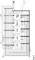
- Fig. 3illustrates datapaths of streaming data in an LTE layer 1 subsystem that comprises a plurality of functional units 10 - 90, in particular digital front end (DFE) unit 10, LTE Tx unit 20, shared RAM unit 30, forward error correction (FEC) data unit 40, fast Fourier transform (FFT) unit 60, parameter estimation unit 70, equalizer unit 80, searcher unit 50, and FEC control unit 90.
- DFEdigital front end
- FECforward error correction
- FFTfast Fourier transform
- parameter estimation unit 70parameter estimation unit 70
- equalizer unit 80equalizer unit 80
- searcher unit 50searcher unit 50
- FEC control unit 90high rate data streams can be distributed using the Simple Streaming Link (SSL) protocol of the invention whichout any addressing.
- SSL data pathsare illustrated in large hatched arrows.
- the low rate and control accesses(illustrated in thin arrows) can be done over a second protocol that comprises addressing, e.g. a AHB based protocol.
- the SSL protocol of the inventioncan also be used for streaming data through functional units of a system implemented in an IC.
- Fig. 4illustrates an exemplary component architecture for any of the functional units 10 - 90 shown in Fig. 3 .
- Each of the functional units 10 - 90may comprises a plurality of sub-components including a local RISC or digital signal processor 440, a plurality of hardware accelerators 421 - 423, and, optionally, at least one memory module 430. Also, each of the functional units may comprise a switching matrix 410 connected between a streaming data input of the respective functional unit and each of said sub-components. The switching matrix can be configured at run time.
- Local processor 440in this application example, is adapted to receive task instructions from a controller 6 of the modem device (shown in Fig. 3 ) over a first bus system using a first protocol.
- the first protocolincludes addressing and may be an AHB based protocol.
- the local processorin response to the task instructions from the controller, configures the sub-components 421 - 423, 430 and switches switching matrix 410 to selectively produce connections between the data streaming input and said sub-components in a manner to perform the dedicated task.
- SSL Signalsare summarized in the following table : Signal Source Sink Description sdata output 1..n bits input 1..n bits Streaming data element. Standard width is 32 bits. The data width is the minimum granularity the SSL supports. svalid output 1 bit input 1 bit The valid/accept handshake is used to drive and stall the communication from source to saccept input 1 bit output 1 bit sink. Source and sink can set or reset these signals at any time. Data is taken over if both are 'high' on the rising edge of the clock. sframe output 1 bit input 1 bit Set to 'high' during one block transfer, e.g. 2048 words of data. The sink can determine the start of the transfer by looking for a rising edge and the end by looking for a falling edge. The svalid signal might not be active in the first cycle. sframe is 'low' after a block transfer.
- the sframe signalIn case the sframe signal is not used by a source, it can clamp the output to "high". In case a sink does not know how to interpret an incoming sframe signal, it can be ignored.
Landscapes
- Engineering & Computer Science (AREA)
- Computer Networks & Wireless Communication (AREA)
- Signal Processing (AREA)
- Communication Control (AREA)
- Mobile Radio Communication Systems (AREA)
- Dc Digital Transmission (AREA)
Description
- The invention relates to a method for transferring data between a data source and a data sink which are controlled by a common clock, wherein the data source and the data sink are functional units of a system built in an integrated circuit.
- Data streaming is known as a method for data transfer.
A simple method to transfer streaming data is by a handshake-type protocol wherein the transmitting entity and the receiving entity synchronize via direct acknowledgment signals. A transmitting party or data source signalizes to be ready for transmission when data are to be sent, and a receiving party or data sink signalizes to be ready for reception when it can or want to process new data. Data transfer does not start unless both the source is ready to transmit and the sink is ready to receive. EP0465221A2 discloses a bus interface using a handshake type transmission protocol. Handshake synchronization is achieved by an interrupt signal which notifies the data source that the last byte of a message has been accepted by a data sink.- The object of the invention is to provide a handshake-based streaming data protocol for intra-circuitry data transfer between and through functional units of a system built in an integrated circuit.
- A particular object of the invention is to provide a data streaming method that can be used in a modem of a wireless communication device and that enables to realize a low power, low size communication device.
- According to the invention there is provided a method for transferring data between a data source and a data sink which are controlled by a common clock. The method is particularly useful for streaming data within a system on an integrated circuit. The method comprises sending a stream of data elements from said source to said sink; simultaneously sending a first binary signal from source to sink, said first signal being low if the data element is to be ignored by the sink and otherwise being high; simultaneously sending a second binary signal from sink to source, said second signal being low if the data element is not accepted by the sink and otherwise being high; and simultaneously sending a third binary signal which marks the beginning and the end of a logical group of data elements within the data stream.
- Additional features and advantages of the present invention will be apparent from the following detailed description of a specific embodiment which is given by way of example only and in which reference will be made to the accompanying drawings, wherein:
- Fig. 1
- shows the signal flow between data source and sink according to one embodiment of the data streaming protocol of the invention;
- Fig. 2
- illustrates one exemplary embodiment of the signal forms of the transfer protocol according to the invention;
- Fig. 3
- illustrates an exemplary embodiment of datapaths between functional units of a circuit device in which the protocol of the invention can be applied; and
- Fig. 4
- shows an exemplary component architecture of any of the functional units of
Fig. 3 . - The invention provides a protocol for high speed data streaming in communication devices which will be referred to as Simple Streaming Link (SSL) below.
- The origin of the data stream is called a 'source' 1, the destination is called a 'sink' 2, as shown in
Fig. 1 . - SSL comprises four signals: sdata, svalid, saccept, sframe, as illustrated in
Fig. 2 . - A stream of data elements that is to be transmitted from
source 1 tosink 2 may have a width of multiple bits, e.g. 7, 16, 24, 32 bits. - A first binary signal, svalid, is sent from source to sink. It is low if the data element is to be ignored by the sink, and otherwise it is high.
- Simultaneously, a second signal, saccept, is sent from sink to source. This second signal is low if the data element is not accepted by the sink, and is otherwise high.
- The svalid and saccept signals thus realize a kind of handshake between source and sink.
- According to the invention, the streaming data protocol comprises a third signal, sframe.
Source 1 andsink 2 must have the same understanding of what the sframe signal means. - Some of the possible uses of the sframe signal are:
- (1) Data transfer only occurs if saccept, svalid and sframe signals are high. The sframe signal marks the beginning and end of a logical group of data elements within the data stream, or a data block transfer.
- (2) Two streams are multiplexed over one link, and the sframe signal is used to distinguish between the first and the second stream.
- (3) The sframe is used to distinguish between data transfer and control transfer.
- (4) The sframe signal is not used in which case the sframe signal is always set to high.
- The source can set the svalid and sframe signals in advance. The sink can set the saccept signal in advance.
- A 'frame' in the sense of the invention is a logical group or sequence of data, such as e.g. an OFDM symbol, a block of control data, a block of information data, etc.
- The sframe signal can be used to/for:
- ▪ mark the beginning and the end of a logical group/sequence
- ▪ Synchronization between functional components of a communication device on data level
- ▪ Differentiate between control and data information.
- ▪ Differentiate between two separate data streams transmitted over the same SSL; for example the third binary signal being high may signify the data belonging to a first logical data stream, and the third binary signal being low may signify the data belonging to a second logical data stream, or vice versa.
- ▪ control purposes, e.g. for dynamic clock gating to decrease power consumption.
- A particular advantage of the invention is, that the sink does not need to count data to detect the end of a logical group or sequence. Also, the SSL protocol of the invention can be used for activity detection and power control. Another application that is contemplated is reconfiguration control of a switching matrix and the accelerators of functional subsystems in an IC modem architecture as described below in conjunction with
Figs. 3 and4 . - In one application example the SSL protocol of the invention is advantageously used for streaming large amounts of data through subsystems of a communication device, e.g. functional units of an LTE modem.
- For example,
Fig. 3 illustrates datapaths of streaming data in anLTE layer 1 subsystem that comprises a plurality of functional units 10 - 90, in particular digital front end (DFE)unit 10,LTE Tx unit 20, sharedRAM unit 30, forward error correction (FEC)data unit 40, fast Fourier transform (FFT)unit 60,parameter estimation unit 70,equalizer unit 80,searcher unit 50, andFEC control unit 90. Here, high rate data streams can be distributed using the Simple Streaming Link (SSL) protocol of the invention whichout any addressing. SSL data paths are illustrated in large hatched arrows. The low rate and control accesses (illustrated in thin arrows) can be done over a second protocol that comprises addressing, e.g. a AHB based protocol. Any of the functional units 10 - 90 may be regarded as adata source 1 ordata sink 2 in the sense of the invention. - The SSL protocol of the invention can also be used for streaming data through functional units of a system implemented in an IC. For example,
Fig. 4 illustrates an exemplary component architecture for any of the functional units 10 - 90 shown inFig. 3 . - Each of the functional units 10 - 90 may comprises a plurality of sub-components including a local RISC or
digital signal processor 440, a plurality of hardware accelerators 421 - 423, and, optionally, at least onememory module 430. Also, each of the functional units may comprise aswitching matrix 410 connected between a streaming data input of the respective functional unit and each of said sub-components. The switching matrix can be configured at run time. Local processor 440, in this application example, is adapted to receive task instructions from acontroller 6 of the modem device (shown inFig. 3 ) over a first bus system using a first protocol. The first protocol includes addressing and may be an AHB based protocol. The local processor, in response to the task instructions from the controller, configures the sub-components 421 - 423, 430 andswitches switching matrix 410 to selectively produce connections between the data streaming input and said sub-components in a manner to perform the dedicated task.- Details on the SSL Signals are summarized in the following table :
Signal Source Sink Description sdata output 1.. n bits input 1..n bits Streaming data element. Standard width is 32 bits. The data width is the minimum granularity the SSL supports. svalid output 1 bit input 1 bit The valid/accept handshake is used to drive and stall the communication from source to saccept input 1 bit output 1 bit sink. Source and sink can set or reset these signals at any time. Data is taken over if both are 'high' on the rising edge of the clock. sframe output 1 bit input 1 bit Set to 'high' during one block transfer, e.g. 2048 words of data. The sink can determine the start of the transfer by looking for a rising edge and the end by looking for a falling edge. The svalid signal might not be active in the first cycle. sframe is 'low' after a block transfer. - In case the sframe signal is not used by a source, it can clamp the output to "high". In case a sink does not know how to interpret an incoming sframe signal, it can be ignored.
Claims (7)
- A method for transferring data between a data source (1) and a data sink (2) which are controlled by a common clock (3), wherein the data source and the data sink are functional units of a system built in an integrated circuit, comprising:sending a stream of data elements from said source to said sink;simultaneously sending a first binary signal (svalid) from source to sink, said first signal being low if the data element is to be ignored by the sink and otherwise being high;simultaneously sending a second binary signal from sink to source (saccept), said second signal being low if the data element is not accepted by the sink and otherwise being high;
characterized bysimultaneously sending a third binary signal (sframe) from said source (1) to said sink (2), wherein the third signal marks the beginning and the end of a logical group of data elements within the data stream, wherein the third binary signal being high signifies the data belonging to a first logical data stream and the third binary signal being low signifies the data belonging to a second logical data stream. - The method of claim 1 wherein a data transfer from source to sink only happens if the first binary signal, the second binary signal and the third binary signal are high.
- The method of claim 1 wherein the third binary signal is ignored by the sink.
- The method of claim 1 wherein the third binary signal is always set to high by the source.
- The method of claim 1 wherein said sink determines the start of the logical group of data elements by detecting a rising edge and the end by detecting a falling edge of the third binary signal.
- The method according to any of claims 1 to 5 wherein the source and the sink are functional units of a wireless communication device.
- The method of claim 6 wherein the functional unit is one of a group consisting of digital front end (DFE) unit, LTE Tx unit, shared RAM unit, forward error correction (FEC) data unit, fast Fourier transform (FFT) unit, parameter estimation unit, equalizer unit, searcher unit, FEC control unit of an LTE modem device, accelerator component, memory module component, RISC processor component, and DSP processor component.
Priority Applications (1)
| Application Number | Priority Date | Filing Date | Title |
|---|---|---|---|
| EP10197315.4AEP2341445B1 (en) | 2009-12-30 | 2010-12-29 | Method for high speed data transfer |
Applications Claiming Priority (2)
| Application Number | Priority Date | Filing Date | Title |
|---|---|---|---|
| EP09016149 | 2009-12-30 | ||
| EP10197315.4AEP2341445B1 (en) | 2009-12-30 | 2010-12-29 | Method for high speed data transfer |
Publications (2)
| Publication Number | Publication Date |
|---|---|
| EP2341445A1 EP2341445A1 (en) | 2011-07-06 |
| EP2341445B1true EP2341445B1 (en) | 2017-09-06 |
Family
ID=43901661
Family Applications (1)
| Application Number | Title | Priority Date | Filing Date |
|---|---|---|---|
| EP10197315.4AActiveEP2341445B1 (en) | 2009-12-30 | 2010-12-29 | Method for high speed data transfer |
Country Status (3)
| Country | Link |
|---|---|
| US (1) | US8769165B2 (en) |
| EP (1) | EP2341445B1 (en) |
| CN (1) | CN102123025B (en) |
Families Citing this family (1)
| Publication number | Priority date | Publication date | Assignee | Title |
|---|---|---|---|---|
| US11068248B2 (en)* | 2019-03-11 | 2021-07-20 | International Business Machines Corporation | Staggering a stream application's deployment |
Family Cites Families (33)
| Publication number | Priority date | Publication date | Assignee | Title |
|---|---|---|---|---|
| US4373183A (en)* | 1980-08-20 | 1983-02-08 | Ibm Corporation | Bus interface units sharing a common bus using distributed control for allocation of the bus |
| US4337463A (en)* | 1980-08-22 | 1982-06-29 | Control Data Corporation | Time synchronization master station and remote station system |
| US4665518A (en)* | 1984-02-13 | 1987-05-12 | Fmc Corporation | Synchronous/asynchronous communication system |
| DE3780634T2 (en)* | 1987-09-10 | 1993-03-11 | Ibm | DATA TRANSFER SYSTEM WITH DIGITAL ALARM. |
| IL96808A (en)* | 1990-04-18 | 1996-03-31 | Rambus Inc | Integrated circuit i/o using a high performance bus interface |
| US5287528A (en)* | 1990-07-03 | 1994-02-15 | National Instruments Corporation | IEEE 488 interface for message handling method |
| JPH05324544A (en)* | 1992-05-15 | 1993-12-07 | Hitachi Ltd | Bus control method |
| DE19621902A1 (en)* | 1996-05-31 | 1997-12-04 | Bosch Gmbh Robert | Information overlay system |
| EP0841766B1 (en)* | 1996-11-08 | 2001-05-09 | Alcatel | Method to synchronise data transmission between a receiver and a transmitter |
| US6075814A (en)* | 1997-05-09 | 2000-06-13 | Broadcom Homenetworking, Inc. | Method and apparatus for reducing signal processing requirements for transmitting packet-based data with a modem |
| US6336159B1 (en)* | 1997-06-25 | 2002-01-01 | Intel Corporation | Method and apparatus for transferring data in source-synchronous protocol and transferring signals in common clock protocol in multiple agent processing system |
| US6665807B1 (en)* | 1998-09-04 | 2003-12-16 | Hitachi, Ltd. | Information processing apparatus |
| JP3592547B2 (en)* | 1998-09-04 | 2004-11-24 | 株式会社ルネサステクノロジ | Information processing apparatus and signal transfer method |
| CN1212010C (en)* | 2000-10-17 | 2005-07-20 | 皇家菲利浦电子有限公司 | Multi-standard channel decoder |
| US6735247B2 (en)* | 2001-03-30 | 2004-05-11 | Qualcomm, Incorporated | Method and apparatus in a communication system |
| US6892314B2 (en)* | 2001-04-02 | 2005-05-10 | International Business Machines Corporation | Method and system of automatic delay detection and receiver adjustment for synchronous bus interface |
| US7016668B2 (en)* | 2001-09-26 | 2006-03-21 | Koninklijke Philips Electronics N.V. | Method and apparatus for a reconfigurable multi-media system |
| JP3898694B2 (en)* | 2001-10-02 | 2007-03-28 | 株式会社日立製作所 | Serial data transmission device |
| US6898723B2 (en)* | 2002-04-01 | 2005-05-24 | Mitac International Corp. | Method for verifying clock signal frequency of computer sound interface that involves checking whether count value of counter is within tolerable count range |
| US7320037B1 (en)* | 2002-05-10 | 2008-01-15 | Altera Corporation | Method and apparatus for packet segmentation, enqueuing and queue servicing for multiple network processor architecture |
| US7949777B2 (en)* | 2002-11-01 | 2011-05-24 | Avid Technology, Inc. | Communication protocol for controlling transfer of temporal data over a bus between devices in synchronization with a periodic reference signal |
| US7103320B2 (en)* | 2003-04-19 | 2006-09-05 | International Business Machines Corporation | Wireless communication system within a system on a chip |
| JP4361565B2 (en)* | 2004-09-21 | 2009-11-11 | 株式会社日立コミュニケーションテクノロジー | Node device, packet control device, wireless communication device, and transmission control method |
| US8301820B2 (en)* | 2005-03-31 | 2012-10-30 | Stmicroelectronics Belgium N.V. | Direct memory access for advanced high speed bus |
| US7415595B2 (en)* | 2005-05-24 | 2008-08-19 | Coresonic Ab | Data processing without processor core intervention by chain of accelerators selectively coupled by programmable interconnect network and to memory |
| US7675928B2 (en)* | 2005-12-15 | 2010-03-09 | Intel Corporation | Increasing cache hits in network processors using flow-based packet assignment to compute engines |
| DE102006022284A1 (en)* | 2006-05-11 | 2007-11-15 | Sick Stegmann Gmbh | Method for synchronizing a bidirectional transmission of data |
| US8027421B2 (en)* | 2006-09-21 | 2011-09-27 | Analog Devices, Inc. | Serial digital data communication interface for transmitting data bits each having a width of multiple clock cycles |
| EP2148178B1 (en)* | 2008-07-23 | 2012-04-18 | SICK STEGMANN GmbH | Digital, bidirectional data transfer method |
| US8059745B2 (en)* | 2008-08-06 | 2011-11-15 | Texas Instruments Incorporated | Sharing logic circuitry for a maximum likelihood MIMO decoder and a viterbi decoder |
| EP2341681A3 (en)* | 2009-12-30 | 2011-12-28 | Blue Wonder Communications GmbH | Modem architecture |
| EP2360548A3 (en)* | 2010-02-12 | 2013-01-30 | Blue Wonder Communications GmbH | Method and device for clock gate controlling |
| US8867680B2 (en)* | 2010-02-12 | 2014-10-21 | Intel Mobile Communications GmbH | Circuitry system and method for connecting synchronous clock domains of the circuitry system |
- 2010
- 2010-12-29EPEP10197315.4Apatent/EP2341445B1/enactiveActive
- 2010-12-30CNCN201010624591.1Apatent/CN102123025B/enactiveActive
- 2010-12-30USUS12/981,680patent/US8769165B2/ennot_activeExpired - Fee Related
Non-Patent Citations (1)
| Title |
|---|
| None* |
Also Published As
| Publication number | Publication date |
|---|---|
| US20110161536A1 (en) | 2011-06-30 |
| CN102123025B (en) | 2015-07-15 |
| US8769165B2 (en) | 2014-07-01 |
| CN102123025A (en) | 2011-07-13 |
| EP2341445A1 (en) | 2011-07-06 |
Similar Documents
| Publication | Publication Date | Title |
|---|---|---|
| US8867680B2 (en) | Circuitry system and method for connecting synchronous clock domains of the circuitry system | |
| EP2791810B1 (en) | System and method of sending data via a plurality of data lines on a bus | |
| US20130117639A1 (en) | Cable interconnection techniques | |
| US10243596B1 (en) | Radio frequency transceiver having digital pre-distortion feedback | |
| US7672326B1 (en) | Serial media independent interface with double data rate | |
| US20100257293A1 (en) | Route Lookup System, Ternary Content Addressable Memory, and Network Processor | |
| CN101242284B (en) | Communication method and network device based on SPI bus | |
| KR20000005871A (en) | Parallel backplane physical layer interface with scalable data bandwidth | |
| US8699623B2 (en) | Modem architecture | |
| US20150186201A1 (en) | Robust link training protocol | |
| JP3989376B2 (en) | Communications system | |
| EP2341445B1 (en) | Method for high speed data transfer | |
| CN105306421A (en) | PCI-E interface based signal processing method and PCI-E interface based signal processing device | |
| US9170952B1 (en) | Configurable multi-standard device interface | |
| CN114490474B (en) | A system for implementing multi-channel UART interface expansion through CPLD | |
| CN110471882A (en) | A kind of monobus telecommunication circuit and method | |
| CN112732602B (en) | Electronic device, network exchanger and interrupt transmission and receiving method | |
| US7831810B2 (en) | Communicating signals between semiconductor chips using round-robin-coupled micropipelines | |
| US7512075B1 (en) | Method and apparatus for collecting statistical information from a plurality of packet processing blocks | |
| US7869491B2 (en) | Data transceiver and method thereof | |
| JP3745758B2 (en) | Flow control method and system | |
| US20250147543A1 (en) | Interface device and operating method thereof | |
| CN110769125A (en) | Communication protocol selection method and device suitable for processing chip | |
| US7788429B2 (en) | Cross coupled unidirectional data ring | |
| CN1681253A (en) | Communication system and method inside the device |
Legal Events
| Date | Code | Title | Description |
|---|---|---|---|
| PUAI | Public reference made under article 153(3) epc to a published international application that has entered the european phase | Free format text:ORIGINAL CODE: 0009012 | |
| AK | Designated contracting states | Kind code of ref document:A1 Designated state(s):AL AT BE BG CH CY CZ DE DK EE ES FI FR GB GR HR HU IE IS IT LI LT LU LV MC MK MT NL NO PL PT RO RS SE SI SK SM TR | |
| AX | Request for extension of the european patent | Extension state:BA ME | |
| 17P | Request for examination filed | Effective date:20120106 | |
| RAP1 | Party data changed (applicant data changed or rights of an application transferred) | Owner name:INTEL MOBILE COMMUNICATIONS GMBH | |
| RAP1 | Party data changed (applicant data changed or rights of an application transferred) | Owner name:INTEL DEUTSCHLAND GMBH | |
| 17Q | First examination report despatched | Effective date:20160420 | |
| GRAP | Despatch of communication of intention to grant a patent | Free format text:ORIGINAL CODE: EPIDOSNIGR1 | |
| INTG | Intention to grant announced | Effective date:20170309 | |
| GRAS | Grant fee paid | Free format text:ORIGINAL CODE: EPIDOSNIGR3 | |
| GRAA | (expected) grant | Free format text:ORIGINAL CODE: 0009210 | |
| AK | Designated contracting states | Kind code of ref document:B1 Designated state(s):AL AT BE BG CH CY CZ DE DK EE ES FI FR GB GR HR HU IE IS IT LI LT LU LV MC MK MT NL NO PL PT RO RS SE SI SK SM TR | |
| REG | Reference to a national code | Ref country code:GB Ref legal event code:FG4D | |
| REG | Reference to a national code | Ref country code:CH Ref legal event code:EP Ref country code:AT Ref legal event code:REF Ref document number:926568 Country of ref document:AT Kind code of ref document:T Effective date:20170915 | |
| REG | Reference to a national code | Ref country code:IE Ref legal event code:FG4D | |
| REG | Reference to a national code | Ref country code:DE Ref legal event code:R096 Ref document number:602010044980 Country of ref document:DE | |
| REG | Reference to a national code | Ref country code:FR Ref legal event code:PLFP Year of fee payment:8 | |
| REG | Reference to a national code | Ref country code:NL Ref legal event code:FP | |
| REG | Reference to a national code | Ref country code:LT Ref legal event code:MG4D | |
| PG25 | Lapsed in a contracting state [announced via postgrant information from national office to epo] | Ref country code:HR Free format text:LAPSE BECAUSE OF FAILURE TO SUBMIT A TRANSLATION OF THE DESCRIPTION OR TO PAY THE FEE WITHIN THE PRESCRIBED TIME-LIMIT Effective date:20170906 Ref country code:FI Free format text:LAPSE BECAUSE OF FAILURE TO SUBMIT A TRANSLATION OF THE DESCRIPTION OR TO PAY THE FEE WITHIN THE PRESCRIBED TIME-LIMIT Effective date:20170906 Ref country code:LT Free format text:LAPSE BECAUSE OF FAILURE TO SUBMIT A TRANSLATION OF THE DESCRIPTION OR TO PAY THE FEE WITHIN THE PRESCRIBED TIME-LIMIT Effective date:20170906 Ref country code:SE Free format text:LAPSE BECAUSE OF FAILURE TO SUBMIT A TRANSLATION OF THE DESCRIPTION OR TO PAY THE FEE WITHIN THE PRESCRIBED TIME-LIMIT Effective date:20170906 Ref country code:NO Free format text:LAPSE BECAUSE OF FAILURE TO SUBMIT A TRANSLATION OF THE DESCRIPTION OR TO PAY THE FEE WITHIN THE PRESCRIBED TIME-LIMIT Effective date:20171206 | |
| REG | Reference to a national code | Ref country code:AT Ref legal event code:MK05 Ref document number:926568 Country of ref document:AT Kind code of ref document:T Effective date:20170906 | |
| PG25 | Lapsed in a contracting state [announced via postgrant information from national office to epo] | Ref country code:BG Free format text:LAPSE BECAUSE OF FAILURE TO SUBMIT A TRANSLATION OF THE DESCRIPTION OR TO PAY THE FEE WITHIN THE PRESCRIBED TIME-LIMIT Effective date:20171206 Ref country code:LV Free format text:LAPSE BECAUSE OF FAILURE TO SUBMIT A TRANSLATION OF THE DESCRIPTION OR TO PAY THE FEE WITHIN THE PRESCRIBED TIME-LIMIT Effective date:20170906 Ref country code:RS Free format text:LAPSE BECAUSE OF FAILURE TO SUBMIT A TRANSLATION OF THE DESCRIPTION OR TO PAY THE FEE WITHIN THE PRESCRIBED TIME-LIMIT Effective date:20170906 Ref country code:GR Free format text:LAPSE BECAUSE OF FAILURE TO SUBMIT A TRANSLATION OF THE DESCRIPTION OR TO PAY THE FEE WITHIN THE PRESCRIBED TIME-LIMIT Effective date:20171207 Ref country code:ES Free format text:LAPSE BECAUSE OF FAILURE TO SUBMIT A TRANSLATION OF THE DESCRIPTION OR TO PAY THE FEE WITHIN THE PRESCRIBED TIME-LIMIT Effective date:20170906 | |
| PG25 | Lapsed in a contracting state [announced via postgrant information from national office to epo] | Ref country code:PL Free format text:LAPSE BECAUSE OF FAILURE TO SUBMIT A TRANSLATION OF THE DESCRIPTION OR TO PAY THE FEE WITHIN THE PRESCRIBED TIME-LIMIT Effective date:20170906 Ref country code:RO Free format text:LAPSE BECAUSE OF FAILURE TO SUBMIT A TRANSLATION OF THE DESCRIPTION OR TO PAY THE FEE WITHIN THE PRESCRIBED TIME-LIMIT Effective date:20170906 Ref country code:CZ Free format text:LAPSE BECAUSE OF FAILURE TO SUBMIT A TRANSLATION OF THE DESCRIPTION OR TO PAY THE FEE WITHIN THE PRESCRIBED TIME-LIMIT Effective date:20170906 | |
| PG25 | Lapsed in a contracting state [announced via postgrant information from national office to epo] | Ref country code:SK Free format text:LAPSE BECAUSE OF FAILURE TO SUBMIT A TRANSLATION OF THE DESCRIPTION OR TO PAY THE FEE WITHIN THE PRESCRIBED TIME-LIMIT Effective date:20170906 Ref country code:SM Free format text:LAPSE BECAUSE OF FAILURE TO SUBMIT A TRANSLATION OF THE DESCRIPTION OR TO PAY THE FEE WITHIN THE PRESCRIBED TIME-LIMIT Effective date:20170906 Ref country code:EE Free format text:LAPSE BECAUSE OF FAILURE TO SUBMIT A TRANSLATION OF THE DESCRIPTION OR TO PAY THE FEE WITHIN THE PRESCRIBED TIME-LIMIT Effective date:20170906 Ref country code:AT Free format text:LAPSE BECAUSE OF FAILURE TO SUBMIT A TRANSLATION OF THE DESCRIPTION OR TO PAY THE FEE WITHIN THE PRESCRIBED TIME-LIMIT Effective date:20170906 Ref country code:IS Free format text:LAPSE BECAUSE OF FAILURE TO SUBMIT A TRANSLATION OF THE DESCRIPTION OR TO PAY THE FEE WITHIN THE PRESCRIBED TIME-LIMIT Effective date:20180106 Ref country code:IT Free format text:LAPSE BECAUSE OF FAILURE TO SUBMIT A TRANSLATION OF THE DESCRIPTION OR TO PAY THE FEE WITHIN THE PRESCRIBED TIME-LIMIT Effective date:20170906 | |
| REG | Reference to a national code | Ref country code:DE Ref legal event code:R097 Ref document number:602010044980 Country of ref document:DE | |
| PLBE | No opposition filed within time limit | Free format text:ORIGINAL CODE: 0009261 | |
| STAA | Information on the status of an ep patent application or granted ep patent | Free format text:STATUS: NO OPPOSITION FILED WITHIN TIME LIMIT | |
| PG25 | Lapsed in a contracting state [announced via postgrant information from national office to epo] | Ref country code:DK Free format text:LAPSE BECAUSE OF FAILURE TO SUBMIT A TRANSLATION OF THE DESCRIPTION OR TO PAY THE FEE WITHIN THE PRESCRIBED TIME-LIMIT Effective date:20170906 | |
| REG | Reference to a national code | Ref country code:CH Ref legal event code:PL | |
| 26N | No opposition filed | Effective date:20180607 | |
| PG25 | Lapsed in a contracting state [announced via postgrant information from national office to epo] | Ref country code:SI Free format text:LAPSE BECAUSE OF FAILURE TO SUBMIT A TRANSLATION OF THE DESCRIPTION OR TO PAY THE FEE WITHIN THE PRESCRIBED TIME-LIMIT Effective date:20170906 | |
| REG | Reference to a national code | Ref country code:IE Ref legal event code:MM4A | |
| PG25 | Lapsed in a contracting state [announced via postgrant information from national office to epo] | Ref country code:LU Free format text:LAPSE BECAUSE OF NON-PAYMENT OF DUE FEES Effective date:20171229 Ref country code:MT Free format text:LAPSE BECAUSE OF NON-PAYMENT OF DUE FEES Effective date:20171229 | |
| REG | Reference to a national code | Ref country code:BE Ref legal event code:MM Effective date:20171231 | |
| PG25 | Lapsed in a contracting state [announced via postgrant information from national office to epo] | Ref country code:IE Free format text:LAPSE BECAUSE OF NON-PAYMENT OF DUE FEES Effective date:20171229 | |
| PG25 | Lapsed in a contracting state [announced via postgrant information from national office to epo] | Ref country code:LI Free format text:LAPSE BECAUSE OF NON-PAYMENT OF DUE FEES Effective date:20171231 Ref country code:BE Free format text:LAPSE BECAUSE OF NON-PAYMENT OF DUE FEES Effective date:20171231 Ref country code:CH Free format text:LAPSE BECAUSE OF NON-PAYMENT OF DUE FEES Effective date:20171231 | |
| PG25 | Lapsed in a contracting state [announced via postgrant information from national office to epo] | Ref country code:HU Free format text:LAPSE BECAUSE OF FAILURE TO SUBMIT A TRANSLATION OF THE DESCRIPTION OR TO PAY THE FEE WITHIN THE PRESCRIBED TIME-LIMIT; INVALID AB INITIO Effective date:20101229 Ref country code:MC Free format text:LAPSE BECAUSE OF FAILURE TO SUBMIT A TRANSLATION OF THE DESCRIPTION OR TO PAY THE FEE WITHIN THE PRESCRIBED TIME-LIMIT Effective date:20170906 | |
| PG25 | Lapsed in a contracting state [announced via postgrant information from national office to epo] | Ref country code:CY Free format text:LAPSE BECAUSE OF NON-PAYMENT OF DUE FEES Effective date:20170906 | |
| PG25 | Lapsed in a contracting state [announced via postgrant information from national office to epo] | Ref country code:MK Free format text:LAPSE BECAUSE OF FAILURE TO SUBMIT A TRANSLATION OF THE DESCRIPTION OR TO PAY THE FEE WITHIN THE PRESCRIBED TIME-LIMIT Effective date:20170906 | |
| PG25 | Lapsed in a contracting state [announced via postgrant information from national office to epo] | Ref country code:TR Free format text:LAPSE BECAUSE OF FAILURE TO SUBMIT A TRANSLATION OF THE DESCRIPTION OR TO PAY THE FEE WITHIN THE PRESCRIBED TIME-LIMIT Effective date:20170906 | |
| PG25 | Lapsed in a contracting state [announced via postgrant information from national office to epo] | Ref country code:PT Free format text:LAPSE BECAUSE OF FAILURE TO SUBMIT A TRANSLATION OF THE DESCRIPTION OR TO PAY THE FEE WITHIN THE PRESCRIBED TIME-LIMIT Effective date:20170906 | |
| PG25 | Lapsed in a contracting state [announced via postgrant information from national office to epo] | Ref country code:AL Free format text:LAPSE BECAUSE OF FAILURE TO SUBMIT A TRANSLATION OF THE DESCRIPTION OR TO PAY THE FEE WITHIN THE PRESCRIBED TIME-LIMIT Effective date:20170906 | |
| P01 | Opt-out of the competence of the unified patent court (upc) registered | Effective date:20230518 | |
| PGFP | Annual fee paid to national office [announced via postgrant information from national office to epo] | Ref country code:NL Payment date:20230925 Year of fee payment:14 | |
| PGFP | Annual fee paid to national office [announced via postgrant information from national office to epo] | Ref country code:FR Payment date:20230921 Year of fee payment:14 | |
| PGFP | Annual fee paid to national office [announced via postgrant information from national office to epo] | Ref country code:GB Payment date:20231006 Year of fee payment:14 | |
| PGFP | Annual fee paid to national office [announced via postgrant information from national office to epo] | Ref country code:DE Payment date:20230919 Year of fee payment:14 | |
| REG | Reference to a national code | Ref country code:DE Ref legal event code:R119 Ref document number:602010044980 Country of ref document:DE | |
| REG | Reference to a national code | Ref country code:NL Ref legal event code:MM Effective date:20250101 | |
| GBPC | Gb: european patent ceased through non-payment of renewal fee | Effective date:20241229 | |
| PG25 | Lapsed in a contracting state [announced via postgrant information from national office to epo] | Ref country code:NL Free format text:LAPSE BECAUSE OF NON-PAYMENT OF DUE FEES Effective date:20250101 |