EP2339828A2 - Sampling and readout of an image sensor - Google Patents
Sampling and readout of an image sensorDownload PDFInfo
- Publication number
- EP2339828A2 EP2339828A2EP10182525AEP10182525AEP2339828A2EP 2339828 A2EP2339828 A2EP 2339828A2EP 10182525 AEP10182525 AEP 10182525AEP 10182525 AEP10182525 AEP 10182525AEP 2339828 A2EP2339828 A2EP 2339828A2
- Authority
- EP
- European Patent Office
- Prior art keywords
- image sensor
- pixels
- sampling
- columns
- column circuits
- Prior art date
- Legal status (The legal status is an assumption and is not a legal conclusion. Google has not performed a legal analysis and makes no representation as to the accuracy of the status listed.)
- Granted
Links
- 238000005070samplingMethods0.000titleclaimsabstractdescription85
- 238000003384imaging methodMethods0.000claimsdescription10
- 238000010586diagramMethods0.000description17
- 238000000034methodMethods0.000description16
- 238000012545processingMethods0.000description15
- 239000003086colorantSubstances0.000description6
- 230000035945sensitivityEffects0.000description5
- 239000003990capacitorSubstances0.000description3
- 239000003574free electronSubstances0.000description3
- 230000006872improvementEffects0.000description3
- 238000005259measurementMethods0.000description3
- 230000008569processEffects0.000description3
- 206010034960PhotophobiaDiseases0.000description2
- 230000008901benefitEffects0.000description2
- 208000013469light sensitivityDiseases0.000description2
- 230000007935neutral effectEffects0.000description2
- 239000004065semiconductorSubstances0.000description2
- 230000003595spectral effectEffects0.000description2
- 239000000758substrateSubstances0.000description2
- 238000012546transferMethods0.000description2
- 238000001429visible spectrumMethods0.000description2
- XUIMIQQOPSSXEZ-UHFFFAOYSA-NSiliconChemical compound[Si]XUIMIQQOPSSXEZ-UHFFFAOYSA-N0.000description1
- 230000003044adaptive effectEffects0.000description1
- 230000000295complement effectEffects0.000description1
- 238000012937correctionMethods0.000description1
- 230000007423decreaseEffects0.000description1
- 230000001747exhibiting effectEffects0.000description1
- 230000006870functionEffects0.000description1
- 239000004973liquid crystal related substanceSubstances0.000description1
- 239000011159matrix materialSubstances0.000description1
- 238000012986modificationMethods0.000description1
- 230000004048modificationEffects0.000description1
- 230000037361pathwayEffects0.000description1
- 230000001105regulatory effectEffects0.000description1
- 230000004044responseEffects0.000description1
- 238000012552reviewMethods0.000description1
- 229910052710siliconInorganic materials0.000description1
- 239000010703siliconSubstances0.000description1
- 238000000638solvent extractionMethods0.000description1
- 230000001360synchronised effectEffects0.000description1
Images


Classifications
- H—ELECTRICITY
- H04—ELECTRIC COMMUNICATION TECHNIQUE
- H04N—PICTORIAL COMMUNICATION, e.g. TELEVISION
- H04N23/00—Cameras or camera modules comprising electronic image sensors; Control thereof
- H04N23/60—Control of cameras or camera modules
- H04N23/667—Camera operation mode switching, e.g. between still and video, sport and normal or high- and low-resolution modes
- H—ELECTRICITY
- H04—ELECTRIC COMMUNICATION TECHNIQUE
- H04N—PICTORIAL COMMUNICATION, e.g. TELEVISION
- H04N25/00—Circuitry of solid-state image sensors [SSIS]; Control thereof
- H04N25/10—Circuitry of solid-state image sensors [SSIS]; Control thereof for transforming different wavelengths into image signals
- H04N25/11—Arrangement of colour filter arrays [CFA]; Filter mosaics
- H04N25/13—Arrangement of colour filter arrays [CFA]; Filter mosaics characterised by the spectral characteristics of the filter elements
- H04N25/133—Arrangement of colour filter arrays [CFA]; Filter mosaics characterised by the spectral characteristics of the filter elements including elements passing panchromatic light, e.g. filters passing white light
- H—ELECTRICITY
- H04—ELECTRIC COMMUNICATION TECHNIQUE
- H04N—PICTORIAL COMMUNICATION, e.g. TELEVISION
- H04N25/00—Circuitry of solid-state image sensors [SSIS]; Control thereof
- H04N25/10—Circuitry of solid-state image sensors [SSIS]; Control thereof for transforming different wavelengths into image signals
- H04N25/11—Arrangement of colour filter arrays [CFA]; Filter mosaics
- H04N25/13—Arrangement of colour filter arrays [CFA]; Filter mosaics characterised by the spectral characteristics of the filter elements
- H04N25/135—Arrangement of colour filter arrays [CFA]; Filter mosaics characterised by the spectral characteristics of the filter elements based on four or more different wavelength filter elements
- H—ELECTRICITY
- H04—ELECTRIC COMMUNICATION TECHNIQUE
- H04N—PICTORIAL COMMUNICATION, e.g. TELEVISION
- H04N25/00—Circuitry of solid-state image sensors [SSIS]; Control thereof
- H04N25/40—Extracting pixel data from image sensors by controlling scanning circuits, e.g. by modifying the number of pixels sampled or to be sampled
- H04N25/42—Extracting pixel data from image sensors by controlling scanning circuits, e.g. by modifying the number of pixels sampled or to be sampled by switching between different modes of operation using different resolutions or aspect ratios, e.g. switching between interlaced and non-interlaced mode
- H—ELECTRICITY
- H04—ELECTRIC COMMUNICATION TECHNIQUE
- H04N—PICTORIAL COMMUNICATION, e.g. TELEVISION
- H04N25/00—Circuitry of solid-state image sensors [SSIS]; Control thereof
- H04N25/40—Extracting pixel data from image sensors by controlling scanning circuits, e.g. by modifying the number of pixels sampled or to be sampled
- H04N25/44—Extracting pixel data from image sensors by controlling scanning circuits, e.g. by modifying the number of pixels sampled or to be sampled by partially reading an SSIS array
- H04N25/443—Extracting pixel data from image sensors by controlling scanning circuits, e.g. by modifying the number of pixels sampled or to be sampled by partially reading an SSIS array by reading pixels from selected 2D regions of the array, e.g. for windowing or digital zooming
- H—ELECTRICITY
- H04—ELECTRIC COMMUNICATION TECHNIQUE
- H04N—PICTORIAL COMMUNICATION, e.g. TELEVISION
- H04N25/00—Circuitry of solid-state image sensors [SSIS]; Control thereof
- H04N25/40—Extracting pixel data from image sensors by controlling scanning circuits, e.g. by modifying the number of pixels sampled or to be sampled
- H04N25/46—Extracting pixel data from image sensors by controlling scanning circuits, e.g. by modifying the number of pixels sampled or to be sampled by combining or binning pixels
- H—ELECTRICITY
- H04—ELECTRIC COMMUNICATION TECHNIQUE
- H04N—PICTORIAL COMMUNICATION, e.g. TELEVISION
- H04N25/00—Circuitry of solid-state image sensors [SSIS]; Control thereof
- H04N25/70—SSIS architectures; Circuits associated therewith
- H—ELECTRICITY
- H04—ELECTRIC COMMUNICATION TECHNIQUE
- H04N—PICTORIAL COMMUNICATION, e.g. TELEVISION
- H04N25/00—Circuitry of solid-state image sensors [SSIS]; Control thereof
- H04N25/70—SSIS architectures; Circuits associated therewith
- H04N25/76—Addressed sensors, e.g. MOS or CMOS sensors
- H04N25/766—Addressed sensors, e.g. MOS or CMOS sensors comprising control or output lines used for a plurality of functions, e.g. for pixel output, driving, reset or power
- H—ELECTRICITY
- H04—ELECTRIC COMMUNICATION TECHNIQUE
- H04N—PICTORIAL COMMUNICATION, e.g. TELEVISION
- H04N25/00—Circuitry of solid-state image sensors [SSIS]; Control thereof
- H04N25/70—SSIS architectures; Circuits associated therewith
- H04N25/76—Addressed sensors, e.g. MOS or CMOS sensors
- H04N25/767—Horizontal readout lines, multiplexers or registers
- H—ELECTRICITY
- H04—ELECTRIC COMMUNICATION TECHNIQUE
- H04N—PICTORIAL COMMUNICATION, e.g. TELEVISION
- H04N25/00—Circuitry of solid-state image sensors [SSIS]; Control thereof
- H04N25/70—SSIS architectures; Circuits associated therewith
- H04N25/76—Addressed sensors, e.g. MOS or CMOS sensors
- H04N25/77—Pixel circuitry, e.g. memories, A/D converters, pixel amplifiers, shared circuits or shared components
- H04N25/778—Pixel circuitry, e.g. memories, A/D converters, pixel amplifiers, shared circuits or shared components comprising amplifiers shared between a plurality of pixels, i.e. at least one part of the amplifier must be on the sensor array itself
- H—ELECTRICITY
- H04—ELECTRIC COMMUNICATION TECHNIQUE
- H04N—PICTORIAL COMMUNICATION, e.g. TELEVISION
- H04N25/00—Circuitry of solid-state image sensors [SSIS]; Control thereof
- H04N25/70—SSIS architectures; Circuits associated therewith
- H04N25/76—Addressed sensors, e.g. MOS or CMOS sensors
- H04N25/78—Readout circuits for addressed sensors, e.g. output amplifiers or A/D converters
- H—ELECTRICITY
- H04—ELECTRIC COMMUNICATION TECHNIQUE
- H04N—PICTORIAL COMMUNICATION, e.g. TELEVISION
- H04N23/00—Cameras or camera modules comprising electronic image sensors; Control thereof
- H04N23/60—Control of cameras or camera modules
- H04N23/63—Control of cameras or camera modules by using electronic viewfinders
- H04N23/631—Graphical user interfaces [GUI] specially adapted for controlling image capture or setting capture parameters
- H04N23/632—Graphical user interfaces [GUI] specially adapted for controlling image capture or setting capture parameters for displaying or modifying preview images prior to image capturing, e.g. variety of image resolutions or capturing parameters
Definitions
- the present inventionrelates generally to electronic image sensors for use in digital cameras and other image capture devices, and more particularly to sampling and readout techniques for use with an electronic image sensor.
- a typical electronic image sensorcomprises a number of light sensitive picture elements ("pixels") arranged in a two-dimensional array. Such an image sensor may be configured to produce a color image by forming a color filter array (CFA) over the pixels.
- CFAcolor filter array
- One commonly used type of CFA patternis the Bayer pattern, disclosed in U.S. Patent No. 3,971,065 , entitled “Color Imaging Array,” which is incorporated by reference herein.
- the Bayer CFA patternprovides each pixel with color photoresponse exhibiting a predominant sensitivity to one of three designated portions of the visible spectrum. The three designated portions may be, for example, red, green and blue, or cyan, magenta and yellow.
- a given CFA patternis generally characterized by a minimal repeating unit in the form of a subarray of contiguous pixels that acts as a basic building block for the pattern. Multiple copies of the minimal repeating unit are juxtaposed to form the complete pattern.
- sampling and readout of the pixels of an image sensor having a Bayer CFA patternwill generally sample all the pixels in a given row into column circuits, and then the entire row of pixels would be read from the column circuits in a single operation.
- the sampling and readoutproceeds in this manner in order to preserve the pixel order of the Bayer CFA pattern in the readout data.
- U.S. Patent Application Publication No. 2007/0024931entitled “Image Sensor with Improved Light Sensitivity,” which is incorporated by reference herein, discloses improved CFA patterns, including patterns which provide certain of the pixels with a panchromatic photoresponse. Such patterns are also generally referred to herein as “sparse" CFA patterns.
- a panchromatic photoresponsehas a wider spectral sensitivity than those spectral sensitivities represented in the selected set of color photoresponses and may, for example, have high sensitivity across substantially the entire visible spectrum.
- Image sensors configured with the improved CFA patternsexhibit greater light sensitivity and are thus well-suited for use in applications involving low scene lighting, short exposure time, small aperture, or other restrictions on the amount of light reaching the image sensor.
- Illustrative embodiments of the inventionprovide sampling and readout techniques that are particularly well-suited for use with image sensors having sparse CFA patterns.
- an image sensorcomprises an array of pixels arranged in rows and columns, with the columns being separated into groups each comprising two or more columns that share a common output.
- the image sensorfurther comprises sampling and readout circuitry that includes, for each group of columns in the pixel array, a corresponding set of two or more column circuits.
- the sampling and readout circuitryis configured to sample the common output for each group of columns independently into one of the column circuits associated with that group, and to read out the common output for each group of columns as previously sampled into another of the column circuits associated with that group.
- the sampling and readout circuitrymay be configured to sample the common output for a given one of the groups of columns into one of the plurality of column circuits associated with the given group concurrently with reading out of the common output for the given group as previously sampled into another of the plurality of column circuits associated with the given group.
- the pixel array of the image sensoris configured in accordance with sparse CFA pattern color having a minimal repeating unit including a plurality of cells, each including a plurality of same-color pixels and a plurality of panchromatic pixels.
- each of the cellsmay comprise four pixels with two same-color pixels arranged diagonally relative to one another and two panchromatic pixels arranged diagonally relative to one another.
- the sampling and readout circuitrymay be configured in an embodiment of this type such that the color pixels in a given one of the cells are sampled and read out using different column circuits than the panchromatic pixels in the given cell.
- An image sensor in accordance with the inventionmay be advantageously implemented in a digital camera or other type of image capture device, and considerably facilitates image generation and associated processing operations in a wide variety of different operating modes.
- the operating modesmay include, for example, full resolution modes with or without color binning, quarter-resolution modes with panchromatic binning and color binning, double sampling modes, video modes, fast autofocus modes, etc.
- FIG. 1shows a digital camera in which sampling and readout techniques are implemented in an illustrative embodiment of the invention.
- the imaging stage 11comprises lens 12, neutral density (ND) filter 13, iris 14 and shutter 18.
- the light 10is focused by lens 12 to form an image on an image sensor 20.
- the amount of light reaching the image sensor 20is regulated by iris 14, ND filter 13 and the time that shutter 18 is open.
- Image sensor 20converts the incident light to an electrical signal for each pixel.
- the image sensor 20may be, for example, a charge coupled device (CCD) type or active pixel sensor (APS) type image sensor, although other types of image sensors may be used in implementing the invention.
- CCDcharge coupled device
- APSactive pixel sensor
- CMOS image sensorsAPS type image sensors fabricated using a complementary metal-oxide-semiconductor (CMOS) process are often referred to as CMOS image sensors.
- the image sensor 20generally has a two-dimensional array of color and panchromatic pixels configured in accordance with a sparse CFA pattern. Examples of sparse CFA patterns that may be used with the image sensor 20 include those described in the above-cited U.S. Patent Application Publication No. 2007/0024931 , although other CFA patterns may be used in other embodiments of the invention.
- An analog signal from image sensor 20is processed by analog signal processor 22 and applied to analog to digital (A/D) converter 24.
- Timing generator 26produces various clocking signals to select particular rows and columns of the pixel array for processing, and synchronizes the operation of analog signal processor 22 and A/D converter 24.
- the image sensor 20, analog signal processor 22, A/D converter 24, and timing generator 26collectively form an image sensor stage 28 of the digital camera.
- the components of image sensor stage 28may comprise separately fabricated integrated circuits, or they may be fabricated as a single integrated circuit as is commonly done with CMOS image sensors.
- the A/D converter 24outputs a stream of digital pixel values that are supplied via a bus 30 to a memory 32 associated with a digital signal processor (DSP) 36.
- Memory 32may comprise any type of memory, such as, for example, synchronous dynamic random access memory (SDRAM).
- SDRAMsynchronous dynamic random access memory
- the DSP 36is one of a plurality of processing elements of the digital camera that are indicated as collectively comprising a processing stage 38.
- the other processing elements of the processing stage 38include exposure controller 40 and system controller 50. Although this partitioning of digital camera functional control among multiple processing elements is typical, these elements may be combined in various ways without affecting the functional operation of the camera and the application of the present invention.
- a given one of the processing elements of processing stage 38can comprise one or more DSP devices, microcontrollers, programmable logic devices, or other digital logic circuits. Although a combination of three separate processing elements is shown in the figure, alternative embodiments may combine the functionality of two or more of these elements into a single processor, controller or other processing element. Sampling and readout techniques as described herein may be implemented at least in part in the form of software that is executed by one or more such processing elements.
- the exposure controller 40is responsive to an indication of an amount of light available in the scene, as determined by brightness sensor 42, and provides appropriate control signals to the ND filter 13, iris 14 and shutter 18 of the imaging stage 11.
- the system controller 50is coupled via a bus 52 to DSP 36 and to program memory 54, system memory 56, host interface 57 and memory card interface 60.
- the system controller 50controls the overall operation of the digital camera based on one or more software programs stored in program memory 54, which may comprise Flash electrically erasable programmable read-only memory (EEPROM) or other nonvolatile memory. This memory is also used to store image sensor calibration data, user setting selections and other data which must be preserved when the camera is turned off.
- System controller 50controls the sequence of image capture by directing exposure controller 40 to operate the lens 12, ND filter 13, iris 14, and shutter 18 as previously described, directing the timing generator 26 to operate the image sensor 20 and associated elements, and directing DSP 36 to process the captured image data.
- DSP 36manipulates the digital image data in its memory 32 according to one or more software programs stored in program memory 54 and copied to memory 32 for execution during image capture.
- the resulting image file stored in memory 32may be, for example, transferred via host interface 57 to an external host computer, transferred via memory card interface 60 and memory card socket 62 to removable memory card 64, or displayed for the user on an image display 65.
- the image display 65is typically an active matrix color liquid crystal display (LCD), although other types of displays may be used.
- the digital camerafurther comprises a user control and status interface 68 including a viewfinder display 70, an exposure display 72, user inputs 74 and status display 76. These elements may be controlled by a combination of software programs executed on exposure controller 40 and system controller 50.
- the user inputs 74typically include some combination of buttons, rocker switches, joysticks, rotary dials or touchscreens.
- Exposure controller 40operates light metering, exposure mode, autofocus and other exposure functions.
- the system controller 50manages a graphical user interface (GUI) presented on one or more of the displays, e.g., on image display 65.
- the GUItypically includes menus for making various option selections and review modes for examining captured images.
- Processed imagesmay be copied to a display buffer in system memory 56 and continuously read out via video encoder 80 to produce a video signal.
- This signalmay be output directly from the camera for display on an external monitor, or processed by display controller 82 and presented on image display 65.
- the digital camera as shown in FIG. 1may comprise additional or alternative elements of a type known to those skilled in the art. Elements not specifically shown or described herein may be selected from those known in the art.
- the present inventionmay be implemented in a wide variety of other types of digital cameras or image capture devices. For example, the present invention can be implemented in imaging applications involving mobile phones and automotive vehicles.
- certain aspects of the embodiments described hereinmay be implemented at least in part in the form of software executed by one or more processing elements of an image capture device. Such software can be implemented in a straightforward manner given the teachings provided herein, as will be appreciated by those skilled in the art.
- the image sensor 20 shown in FIG. 1includes a two-dimensional array of light sensitive pixels fabricated on a silicon substrate that provide a way of converting incoming light at each pixel into an electrical signal that is measured. As the sensor is exposed to light, free electrons are generated and captured within the electronic structure at each pixel. Capturing these free electrons for some period of time and then measuring the number of electrons captured, or measuring the rate at which free electrons are generated, allows the light level at each pixel to be measured. In the former case, accumulated charge is shifted out of the array of pixels to a charge to voltage measurement circuit as in a CCD type image sensor, or the area close to each pixel contains elements of a charge to voltage measurement circuit as in an APS type or CMOS image sensor.
- image sensor 20Whenever general reference is made to an image sensor in the following description, it is understood to be representative of the image sensor 20 from FIG. 1 . It is further understood that all examples and their equivalents of image sensor architectures and pixel patterns of the present invention disclosed in this specification are used for image sensor 20.
- a pixelrefers to a discrete light sensing area and charge shifting or charge measurement circuitry associated with the light sensing area.
- the term pixelcommonly refers to a particular location in the image having associated color values.
- FIG. 2shows a portion of a pixel array 100 in the image sensor 20 of the digital camera of FIG. 1 in an illustrative embodiment.
- Each pixel 102 of the pixel array 100comprises a photodiode 104 and a transfer gate (TG) 106.
- Additional circuitry 108comprising multiple transistors is shared by a subarray of four pixels arranged in a 2x2 block.
- the 2x2 pixel blockis one example of what is more generally referred to herein as a "cell.”
- the configuration of pixel array 100 in this embodimentis referred to as a four transistor, four shared (4T4S) arrangement, as four of the pixels and their associated four TGs share the additional circuitry 108.
- Adjacent each of the pixels 102 in the array 100is an indicator of the corresponding color, which may be red (R), blue (B), green (G) or panchromatic (P), in accordance with a designated sparse CFA pattern of the image sensor 20.
- the particular sparse CFA pattern used in the illustrative embodiments described hereinis a panchromatic checkerboard pattern disclosed in the above-cited U.S. Patent Application Publication No. 2007/0024931 , although numerous other CFA patterns may be used.
- the portion of the array 100 shown in FIG. 2includes four rows of eight pixels each, with the two upper rows of this portion being referred to herein as a blue/green row pair, and the two lower rows being referred to herein as a red/green row pair.
- the minimal repeating unit in this particular CFA patternis a subarray of 16 contiguous pixels comprising the left half or right half of the portion of the pixel array 100 as shown in FIG. 2 .
- the minimal repeating unitcomprises 16 pixels arranged in four four-pixel cells as follows: where P represents one of the panchromatic pixels and X, Y and Z represent respective color pixels. In this particular embodiment, X, Y and Z are red, green and blue, respectively.
- X, Y and Zmay be individually selected in a different manner from red, green and blue, or may be individually selected from another set of colors, such as cyan, magenta and yellow. Patterns with other minimal repeating units, such as minimal repeating units of at least twelve pixels as described in the above-cited U.S. Patent Application Publication No. 2007/0024931 , may be used.
- the columns in the portion of the pixel array 100 shown in FIG. 2are separated into groups, with each group comprising two of the columns and sharing a common output.
- each groupcomprising two of the columns and sharing a common output.
- the pixels in the first two columns at the left side of the arrayshare a common output denoted PixCol 0/1 .
- the pixels in the next two columns of the arrayshare a common output denoted PixCol 2/3 .
- the remaining two pairs of columnsshare the respective common outputs denoted PixCo1 4/5 and PixCol 6/7 .
- Each pixel in a given one of the 2x2 pixel cellsis connectable to its shared common output via the additional circuitry 108 associated with that cell.
- the additional circuitry 108 in this embodimentcomprises three N-type metal-oxide-semiconductor (NMOS) transistors interconnected as shown.
- NMOSN-type metal-oxide-semiconductor
- different types of column groupings, pixel cells and shared outputs, as well as circuitry for connecting the pixel cells to the shared outputs,may be used.
- Control signals applied to the pixel arrayinclude TG control signals TG_P0, TG_C1, TG_C2 and TG_P3, as well as additional control signals including row select (RS) signals and reset gate (RG) signals.
- RSrow select
- RGreset gate
- the pixel array 100is advantageously configured to permit binning of same-color pixels and binning of panchromatic pixels.
- binninggenerally refers to simultaneously connecting two or more pixels from the same pixel cell to the same common output prior to sampling that output.
- FIG. 3illustrates exemplary sampling and readout circuitry comprising column circuits 110 that are configured for sampling and readout of particular column pairs and are located at the bottom of the pixel array 100.
- the column circuits 110comprise sample-and-hold switches 112, column circuit capacitors 114, and column output switches 116.
- the sampling and readout circuitry in this embodimentfurther comprises top column circuits, configured in a manner similar to bottom column circuits 110 but not shown in the figure, at the top of the pixel array 100. Top and bottom column circuits configured in the manner illustrated in FIG. 3 will be denoted more specifically herein, for example, in conjunction with FIG. 4 , as top and bottom column circuits 110T and 110B, respectively.
- the shared common outputs PixCol 0/1 through PixCol 14/15 as shown in FIG. 3are coupled to respective column circuits in the set of column circuits 110.
- each such shared common outputis coupled to two distinct column circuits in the present embodiment, with one of the column circuits being a top column circuit and another of the column circuits being a bottom column circuit.
- the two column circuits associated with a given group of two columnsare on opposite sides of the pixel array 100. Again, only those column circuits at the bottom of the pixel array are shown in FIG. 3 .
- the two shared column circuitsmay both be on the same side of the pixel array.
- FIG. 3 diagramOther signals shown in the FIG. 3 diagram include those denoted voltage output signal (VSIG) and voltage output reset (VRST), as well as decode signals DEC K through DEC K+7 , with one of the decode signals associated with each column circuit.
- Each column circuit in this embodimentcomprises a pair of capacitors and the associated switches.
- sampling and readout circuitryis intended to be construed generally, so as to encompass, for example, not only column circuits such as those shown in FIG. 3 , but also other related switching elements associated with the pixel array 100, such as additional circuitry 108. Thus, sampling and readout circuitry in a given embodiment may encompass switches or other elements that are formed integrally with the pixel array. Sampling and readout circuitry is generally implemented within the sensor array 20, for example, as in the case of a CMOS image sensor.
- FIGS. 4 through 13Each of the examples shown in FIGS. 4 through 13 utilizes the same four-row portion of pixel array 100 that is shown in FIG. 2 . It should be appreciated that a given embodiment of the invention may be configured to support all of the various examples to be described, only a subset of one or more of these examples, or one or more variants thereof. Thus, each of the examples to be described may be viewed as a particular operating mode of a given set of sampling and readout circuitry implemented in the digital camera of FIG. 1 .
- FIG. 4generally illustrates the diagrammatical conventions that will be utilized in describing the sampling and readout operations for the remaining figures.
- a portion of the pixel array 100is shown in the figure, configured in accordance with the above-noted panchromatic checkerboard CFA pattern.
- the particular portion of the array that is shown in FIG. 4comprises four rows of eight pixels each, although it is to be understood that sampling and readout operations for the remaining portions of the array are carried out in a similar manner.
- the pixel arrayis assumed to be configured in the 4T4S arrangement described in conjunction with FIG. 2 , and its associated sampling and readout circuitry is assumed to be configured as shown in FIG. 3 .
- the text at the left of the array(“C2") identifies one or more TGs that are being activated in conjunction with the sampling operation for a given 2x2 subarray of shared pixels.
- the "TG Arrangement" diagram on the left side of the figureshows the relationship between TGs and pixels in the 2x2 subarray, with TGs denoted C1 and C2 representing two pixels of the same color and TGs denoted P0 and P3 representing two panchromatic pixels.
- Top and bottom column circuits 110T and 110Bare shown by the rectangles at the top and bottom, respectively, of the pixel array 100.
- the nomenclature in the rectanglesindicates T or B for top or bottom and includes a number for readout address.
- Rightward pointing arrows coming out of the column circuitsindicate which column circuits are being read out.
- the column circuitsare read in sequence.
- the text at the left of the rightward pointing arrows(“Read Odd” or "Read Even") indicates which column circuit addresses are to be read, where, as noted above, the addresses are denoted by the numbers in the column circuit rectangles.
- Lineis used to refer to a readout unit, that is, a set of pixels that are read out in a given readout operation.
- Line 0as shown in FIG. 4 represents a readout unit given by the sequence B0, T1, B2, and T3.
- B0, T1, B2, and T3the sequence of addresses
- Line 0provides readout of half as many pixels (4 in this case) as are contained in a given row in the array (8 in this case).
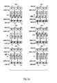
- FIGS. 5A and 5Bshow two different sequences of lines, denoted Option 1 and Option 2, for sampling and readout of the four-row portion of the pixel array 100 at full resolution and without binning of colors. It is apparent that eight lines, denoted Line 0 through Line 7, are required to read out the four rows in each of the two different options.
- FIGS. 6A and 6Bshow two different sequences of lines, again denoted Option 1 and Option 2, for sampling and readout of the four-row portion of the pixel array 100 at full resolution with binning of colors to improve signal-to-noise ratio (SNR) and to improve frame rate. Note that six lines are required to read out the four rows in this example.
- the first four linesare the same.
- the sampling and readout order for the panchromatic pixels in lines 4 and 5is the opposite of that used in Option 1.
- This second optionensures that the panchromatic pixels in the same relative positions in each 2x2 pixel cell are read using the same output channel, regardless of whether a given such panchromatic pixel is from the blue/green row pair or the green/red row pair.
- output channel T0is used in Line 1 to read out a lower left panchromatic pixel 600 in one of the 2x2 pixel cells
- output channel B0is used in Line 4 to read out a lower left panchromatic pixel 602 in another 2x2 pixel cell.
- panchromatic pixels in the same relative position in different 2x2 pixel cellsare read out using different column circuits.
- FIG. 6B sampling and readout arrangementaddresses this issue. For example, it can be seen from this figure that lower left panchromatic pixels 600 and 602 are now both read out using column circuit T0, in Line 1 and Line 5, respectively.
- Such an arrangementmay be preferred in embodiments in which there are differences between the top and bottom column circuits that would otherwise require gain correction or another type of adjustment.
- FIG. 7shows the relationship between the rows of pixels in the four-row portion of the pixel array 100 (left diagram) and the output lines that are read out of the array for full resolution readout using both non-binned color pixels (middle diagram) and binned color pixels (right diagram).
- the middle and right diagramscorrespond respectively to the diagrams "Full Resolution Non-Binned Color (Option 2)" in FIG. 5B and "Full Resolution Binned Color (Option 2)" in FIG. 6B .
- lineis used to refer to a readout unit. It is apparent from FIG. 7 that two lines are required to read out one full resolution row when using non-binned color (middle diagram), with one line comprising all the color pixels from the row and the other line comprising all the panchromatic pixels from the row. Similarly, three lines are required to read out two full resolution rows when using binned color (right diagram), with one line comprising the binned color pixels from the two rows, one line comprising all the panchromatic pixels from one row, and the remaining line comprising all the panchromatic pixels from the other row.
- FIG. 8a sequence of lines is shown for sampling and readout of the four-row portion of the pixel array 100 at full resolution with binning of colors and double sampling.
- This exemplary oversampling arrangementprovides further SNR improvement at the cost of reduced frame rate.
- the figureshows the sampling and readout for only the green/red row pair (i.e., the lower two rows of the four-row portion of the array), it is to be understood that the green/blue row pair (i.e., the upper two rows of the four-row portion of the array) is read out identically to the red/green row pair.
- sampling and readoutare non-concurrent in this example, that is, occur at separate times.
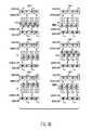
- FIGS. 9A and 9Bshow two different sequences of lines, denoted Option 1 and Option 2, for sampling and readout of the four-row portion of the pixel array 100 at one-quarter resolution and with separate binning of the colors and panchromatic pixels to improve SNR and to improve frame rate.
- Four lines, denoted Line 0 through Line 3,are required to read out the four rows in each of the two different options.
- Option 1as shown in FIG. 9A , green pixels are read out using both top and bottom column circuits. As previously indicated, this type of situation may be undesirable in implementations in which there are differences between the top and bottom column circuits.
- 9Baddresses this issue by ensuring that all green pixels are read out using column circuits on one side of the array, namely, the top column circuits in this example. This eliminates any differences in the green response that would otherwise be attributable to the green pixel pairs being read out of column circuits on both top and bottom of the array.
- FIG. 10shows a sequence of lines for sampling and readout of the four-row portion of the pixel array 100 at one-quarter resolution, with separate binning of the colors and panchromatic pixels, and with double sampling to provide further SNR improvement at the cost of reduced frame rate.
- the sampling and readout in FIG. 10is shown for only the green/red row pair, but it is to be understood that the green/blue row pair is read out identically to the red/green row pair. Also, sampling and readout are again non-concurrent in this example.
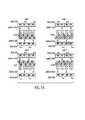
- FIG. 11shows three different line sequences for quarter-resolution video sampling and readout of the four-row portion of pixel array 100. All of these sequences provide output consistent with that which would be provided if a Bayer CFA pattern were used. The differences between the three sequences relate to how many panchromatic pixels are included with the color pixels in the binned result. Including panchromatic pixels with the color pixels increases photographic speed but decreases color saturation.
- the top diagram in FIG. 11shows the color only case, the middle diagram shows a medium desaturation case using one panchromatic pixel for each pair of same-color pixels, and the bottom diagram shows a higher desaturation case using two panchromatic pixels for each pair of same-color pixels.
- FIG. 12another sequence of lines is shown for quarter-resolution video sampling and readout of the four-row portion of pixel array 100.
- double samplingis used to provide SNR improvement at the cost of reduced frame rate.
- Similar sequencescan be used for desaturated video in which one or two panchromatic pixels are binned with each pair of same-color pixels, as in the FIG. 11 examples.
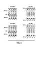
- FIG. 13shows two different sequences of lines for sampling and readout of the four-row portion of the pixel array 100 that are particularly useful in fast autofocus applications.
- the upper diagramshows an arrangement with binning of panchromatic pixels, while the lower diagram shows an arrangement with binning of color pixels and output consistent with a Bayer CFA pattern.
- there is aggressive vertical subsamplingi.e., taking 1 out of every 3 row pairs
- the relatively high horizontal sampling frequency in both casesallows good determination of focus.
- the panchromatic casewill have the best photographic sensitivity, an important consideration given that the high frame rate will limit the exposure time.
- the Bayer output casewill allow the data to be used for both preview and video purposes as well as for determination of focus.
- sampling and readout arrangements of the illustrative embodimentsadvantageously allow the color pixels from a given row pair to be read out separately from the panchromatic pixels.
- the exemplary 2x2 pixel arrangement of FIG. 2 in which two columns of pixels share a common outputmeans that two sampling operations are required to access all the pixels from a given row.
- a sparse CFA patternsuch as the panchromatic checkerboard pattern used in the illustrative embodiments above, improved performance is obtained by reading out the color pixels separately from the panchromatic pixels so as to avoid having to separate them later in memory.
- the above-described techniquesallow the sampling of half a row of pixels (e.g., either the panchromatic pixels or the color pixels) concurrently with the reading out of a previously sampled half row of pixels, effectively eliminating the overhead of the sampling time.
- Another advantageis that the described techniques allow a pair of same-color pixels or a pair of panchromatic pixels to be combined in the charge domain prior to readout, thereby improving SNR and reducing readout time. For example, certain of the techniques require only three sampling and readout operations for each row pair, two for the panchromatic pixels and one for the binned color pixels.
- sampling and readout techniques described hereinare highly flexible, and provide improved performance in a wide variety of applications, including operating modes involving double sampling (i.e., oversampling to improve SNR at the expense of readout time), video and autofocus. These and other additional operating modes may be made selectable in a given image capture device depending on capture conditions, end user preference or other factors.
Landscapes
- Engineering & Computer Science (AREA)
- Multimedia (AREA)
- Signal Processing (AREA)
- Physics & Mathematics (AREA)
- Spectroscopy & Molecular Physics (AREA)
- Color Television Image Signal Generators (AREA)
- Transforming Light Signals Into Electric Signals (AREA)
Abstract
Description
- The present invention relates generally to electronic image sensors for use in digital cameras and other image capture devices, and more particularly to sampling and readout techniques for use with an electronic image sensor.
- A typical electronic image sensor comprises a number of light sensitive picture elements ("pixels") arranged in a two-dimensional array. Such an image sensor may be configured to produce a color image by forming a color filter array (CFA) over the pixels. One commonly used type of CFA pattern is the Bayer pattern, disclosed in
U.S. Patent No. 3,971,065 , entitled "Color Imaging Array," which is incorporated by reference herein. The Bayer CFA pattern provides each pixel with color photoresponse exhibiting a predominant sensitivity to one of three designated portions of the visible spectrum. The three designated portions may be, for example, red, green and blue, or cyan, magenta and yellow. A given CFA pattern is generally characterized by a minimal repeating unit in the form of a subarray of contiguous pixels that acts as a basic building block for the pattern. Multiple copies of the minimal repeating unit are juxtaposed to form the complete pattern. - An image captured using an image sensor with a Bayer CFA pattern has only one color value at each pixel. Therefore, in order to produce a full color image, the missing color values at each pixel are interpolated from the color values of nearby pixels. Numerous such interpolation techniques are known in the art. See, for example,
U.S. Patent No. 5,652,621 , entitled "Adaptive Color Plane Interpolation in Single Sensor Color Electronic Camera," which is incorporated by reference herein. - In accordance with conventional practice, sampling and readout of the pixels of an image sensor having a Bayer CFA pattern will generally sample all the pixels in a given row into column circuits, and then the entire row of pixels would be read from the column circuits in a single operation. The sampling and readout proceeds in this manner in order to preserve the pixel order of the Bayer CFA pattern in the readout data.
U.S. Patent Application Publication No. 2007/0024931 , entitled "Image Sensor with Improved Light Sensitivity," which is incorporated by reference herein, discloses improved CFA patterns, including patterns which provide certain of the pixels with a panchromatic photoresponse. Such patterns are also generally referred to herein as "sparse" CFA patterns. A panchromatic photoresponse has a wider spectral sensitivity than those spectral sensitivities represented in the selected set of color photoresponses and may, for example, have high sensitivity across substantially the entire visible spectrum. Image sensors configured with the improved CFA patterns exhibit greater light sensitivity and are thus well-suited for use in applications involving low scene lighting, short exposure time, small aperture, or other restrictions on the amount of light reaching the image sensor.- Conventional sampling and readout techniques such as those described above in the context of the Bayer CFA pattern can be inefficient when applied to sparse CFA patterns. Accordingly, a need exists for improved sampling and readout techniques for use with sparse CFA patterns.
- Illustrative embodiments of the invention provide sampling and readout techniques that are particularly well-suited for use with image sensors having sparse CFA patterns.
- In accordance with one aspect of the invention, an image sensor comprises an array of pixels arranged in rows and columns, with the columns being separated into groups each comprising two or more columns that share a common output. The image sensor further comprises sampling and readout circuitry that includes, for each group of columns in the pixel array, a corresponding set of two or more column circuits. The sampling and readout circuitry is configured to sample the common output for each group of columns independently into one of the column circuits associated with that group, and to read out the common output for each group of columns as previously sampled into another of the column circuits associated with that group.
- By way of example, the sampling and readout circuitry may be configured to sample the common output for a given one of the groups of columns into one of the plurality of column circuits associated with the given group concurrently with reading out of the common output for the given group as previously sampled into another of the plurality of column circuits associated with the given group.
- In one of the illustrative embodiments, the pixel array of the image sensor is configured in accordance with sparse CFA pattern color having a minimal repeating unit including a plurality of cells, each including a plurality of same-color pixels and a plurality of panchromatic pixels. For example, each of the cells may comprise four pixels with two same-color pixels arranged diagonally relative to one another and two panchromatic pixels arranged diagonally relative to one another. The sampling and readout circuitry may be configured in an embodiment of this type such that the color pixels in a given one of the cells are sampled and read out using different column circuits than the panchromatic pixels in the given cell.
- An image sensor in accordance with the invention may be advantageously implemented in a digital camera or other type of image capture device, and considerably facilitates image generation and associated processing operations in a wide variety of different operating modes. The operating modes may include, for example, full resolution modes with or without color binning, quarter-resolution modes with panchromatic binning and color binning, double sampling modes, video modes, fast autofocus modes, etc.
- The above and other objects, features, and advantages of the present invention will become more apparent when taken in conjunction with the following description and drawings wherein identical reference numerals have been used, where possible, to designate identical features that are common to the figures, and wherein:
FIG. 1 is a block diagram of a digital camera having an image sensor with a sparse CFA pattern and incorporating sampling and readout circuitry in accordance with an illustrative embodiment of the invention;FIG. 2 is a schematic diagram of one possible implementation of a portion of a pixel array in the image sensor of the digital camera ofFIG. 1 ;FIG. 3 shows one possible implementation of sampling and readout circuitry comprising column circuits for sampling and readout of the pixel array ofFIG. 2 ; andFIGS. 4 through 13 show examples of sampling and readout operations applied to the pixel array ofFIG. 2 in illustrative embodiments of the invention.- The present invention will be illustrated herein in conjunction with particular embodiments of image capture devices, image sensors, and associated sampling and readout techniques. It should be understood, however, that these illustrative arrangements are presented by way of example only, and should not be viewed as limiting the scope of the invention in any way. Those skilled in the art will recognize that the disclosed arrangements can be adapted in a straightforward manner for use with a wide variety of other types of image capture devices, image sensors, and associated sampling and readout techniques.
FIG. 1 shows a digital camera in which sampling and readout techniques are implemented in an illustrative embodiment of the invention. In the digital camera,light 10 from a subject scene is input to animaging stage 11. Theimaging stage 11 compriseslens 12, neutral density (ND)filter 13,iris 14 andshutter 18. Thelight 10 is focused bylens 12 to form an image on animage sensor 20. The amount of light reaching theimage sensor 20 is regulated byiris 14,ND filter 13 and the time thatshutter 18 is open.Image sensor 20 converts the incident light to an electrical signal for each pixel. Theimage sensor 20 may be, for example, a charge coupled device (CCD) type or active pixel sensor (APS) type image sensor, although other types of image sensors may be used in implementing the invention. APS type image sensors fabricated using a complementary metal-oxide-semiconductor (CMOS) process are often referred to as CMOS image sensors. Theimage sensor 20 generally has a two-dimensional array of color and panchromatic pixels configured in accordance with a sparse CFA pattern. Examples of sparse CFA patterns that may be used with theimage sensor 20 include those described in the above-citedU.S. Patent Application Publication No. 2007/0024931 , although other CFA patterns may be used in other embodiments of the invention.- An analog signal from
image sensor 20 is processed byanalog signal processor 22 and applied to analog to digital (A/D)converter 24.Timing generator 26 produces various clocking signals to select particular rows and columns of the pixel array for processing, and synchronizes the operation ofanalog signal processor 22 and A/D converter 24. Theimage sensor 20,analog signal processor 22, A/D converter 24, andtiming generator 26 collectively form animage sensor stage 28 of the digital camera. The components ofimage sensor stage 28 may comprise separately fabricated integrated circuits, or they may be fabricated as a single integrated circuit as is commonly done with CMOS image sensors. The A/D converter 24 outputs a stream of digital pixel values that are supplied via abus 30 to amemory 32 associated with a digital signal processor (DSP) 36.Memory 32 may comprise any type of memory, such as, for example, synchronous dynamic random access memory (SDRAM). Thebus 30 provides a pathway for address and data signals and connectsDSP 36 tomemory 32 and A/D converter 24. - The DSP 36 is one of a plurality of processing elements of the digital camera that are indicated as collectively comprising a
processing stage 38. The other processing elements of theprocessing stage 38 includeexposure controller 40 andsystem controller 50. Although this partitioning of digital camera functional control among multiple processing elements is typical, these elements may be combined in various ways without affecting the functional operation of the camera and the application of the present invention. A given one of the processing elements ofprocessing stage 38 can comprise one or more DSP devices, microcontrollers, programmable logic devices, or other digital logic circuits. Although a combination of three separate processing elements is shown in the figure, alternative embodiments may combine the functionality of two or more of these elements into a single processor, controller or other processing element. Sampling and readout techniques as described herein may be implemented at least in part in the form of software that is executed by one or more such processing elements. - The
exposure controller 40 is responsive to an indication of an amount of light available in the scene, as determined bybrightness sensor 42, and provides appropriate control signals to theND filter 13,iris 14 and shutter 18 of theimaging stage 11. - The
system controller 50 is coupled via abus 52 toDSP 36 and to programmemory 54,system memory 56,host interface 57 andmemory card interface 60. Thesystem controller 50 controls the overall operation of the digital camera based on one or more software programs stored inprogram memory 54, which may comprise Flash electrically erasable programmable read-only memory (EEPROM) or other nonvolatile memory. This memory is also used to store image sensor calibration data, user setting selections and other data which must be preserved when the camera is turned off.System controller 50 controls the sequence of image capture by directingexposure controller 40 to operate thelens 12,ND filter 13,iris 14, and shutter 18 as previously described, directing thetiming generator 26 to operate theimage sensor 20 and associated elements, and directingDSP 36 to process the captured image data. - In the illustrated embodiment,
DSP 36 manipulates the digital image data in itsmemory 32 according to one or more software programs stored inprogram memory 54 and copied tomemory 32 for execution during image capture. After an image is captured and processed, the resulting image file stored inmemory 32 may be, for example, transferred viahost interface 57 to an external host computer, transferred viamemory card interface 60 andmemory card socket 62 toremovable memory card 64, or displayed for the user on animage display 65. Theimage display 65 is typically an active matrix color liquid crystal display (LCD), although other types of displays may be used. - The digital camera further comprises a user control and
status interface 68 including aviewfinder display 70, anexposure display 72,user inputs 74 andstatus display 76. These elements may be controlled by a combination of software programs executed onexposure controller 40 andsystem controller 50. Theuser inputs 74 typically include some combination of buttons, rocker switches, joysticks, rotary dials or touchscreens.Exposure controller 40 operates light metering, exposure mode, autofocus and other exposure functions. Thesystem controller 50 manages a graphical user interface (GUI) presented on one or more of the displays, e.g., onimage display 65. The GUI typically includes menus for making various option selections and review modes for examining captured images. - Processed images may be copied to a display buffer in
system memory 56 and continuously read out viavideo encoder 80 to produce a video signal. This signal may be output directly from the camera for display on an external monitor, or processed bydisplay controller 82 and presented onimage display 65. - It is to be appreciated that the digital camera as shown in
FIG. 1 may comprise additional or alternative elements of a type known to those skilled in the art. Elements not specifically shown or described herein may be selected from those known in the art. As noted previously, the present invention may be implemented in a wide variety of other types of digital cameras or image capture devices. For example, the present invention can be implemented in imaging applications involving mobile phones and automotive vehicles. Also, as mentioned above, certain aspects of the embodiments described herein may be implemented at least in part in the form of software executed by one or more processing elements of an image capture device. Such software can be implemented in a straightforward manner given the teachings provided herein, as will be appreciated by those skilled in the art. - The
image sensor 20 shown inFIG. 1 includes a two-dimensional array of light sensitive pixels fabricated on a silicon substrate that provide a way of converting incoming light at each pixel into an electrical signal that is measured. As the sensor is exposed to light, free electrons are generated and captured within the electronic structure at each pixel. Capturing these free electrons for some period of time and then measuring the number of electrons captured, or measuring the rate at which free electrons are generated, allows the light level at each pixel to be measured. In the former case, accumulated charge is shifted out of the array of pixels to a charge to voltage measurement circuit as in a CCD type image sensor, or the area close to each pixel contains elements of a charge to voltage measurement circuit as in an APS type or CMOS image sensor. - Whenever general reference is made to an image sensor in the following description, it is understood to be representative of the
image sensor 20 fromFIG. 1 . It is further understood that all examples and their equivalents of image sensor architectures and pixel patterns of the present invention disclosed in this specification are used forimage sensor 20. - In the context of an image sensor, a pixel refers to a discrete light sensing area and charge shifting or charge measurement circuitry associated with the light sensing area. In the context of a digital color image, the term pixel commonly refers to a particular location in the image having associated color values.
FIG. 2 shows a portion of apixel array 100 in theimage sensor 20 of the digital camera ofFIG. 1 in an illustrative embodiment. Eachpixel 102 of thepixel array 100 comprises aphotodiode 104 and a transfer gate (TG) 106. Additional circuitry 108 comprising multiple transistors is shared by a subarray of four pixels arranged in a 2x2 block. The 2x2 pixel block is one example of what is more generally referred to herein as a "cell." There is a different set of additional circuitry 108 associated with each of the 2x2 pixel cells. The configuration ofpixel array 100 in this embodiment is referred to as a four transistor, four shared (4T4S) arrangement, as four of the pixels and their associated four TGs share the additional circuitry 108. Adjacent each of thepixels 102 in thearray 100 is an indicator of the corresponding color, which may be red (R), blue (B), green (G) or panchromatic (P), in accordance with a designated sparse CFA pattern of theimage sensor 20. The particular sparse CFA pattern used in the illustrative embodiments described herein is a panchromatic checkerboard pattern disclosed in the above-citedU.S. Patent Application Publication No. 2007/0024931 , although numerous other CFA patterns may be used.- The portion of the
array 100 shown inFIG. 2 includes four rows of eight pixels each, with the two upper rows of this portion being referred to herein as a blue/green row pair, and the two lower rows being referred to herein as a red/green row pair. The minimal repeating unit in this particular CFA pattern is a subarray of 16 contiguous pixels comprising the left half or right half of the portion of thepixel array 100 as shown inFIG. 2 . Thus, the minimal repeating unit comprises 16 pixels arranged in four four-pixel cells as follows:where P represents one of the panchromatic pixels and X, Y and Z represent respective color pixels. In this particular embodiment, X, Y and Z are red, green and blue, respectively. Alternatively, X, Y and Z may be individually selected in a different manner from red, green and blue, or may be individually selected from another set of colors, such as cyan, magenta and yellow. Patterns with other minimal repeating units, such as minimal repeating units of at least twelve pixels as described in the above-cited
U.S. Patent Application Publication No. 2007/0024931 , may be used. - The columns in the portion of the
pixel array 100 shown inFIG. 2 are separated into groups, with each group comprising two of the columns and sharing a common output. For example, the pixels in the first two columns at the left side of the array share a common output denoted PixCol0/1. Similarly, the pixels in the next two columns of the array share a common output denoted PixCol2/3. The remaining two pairs of columns share the respective common outputs denoted PixCo14/5 and PixCol6/7. Each pixel in a given one of the 2x2 pixel cells is connectable to its shared common output via the additional circuitry 108 associated with that cell. The additional circuitry 108 in this embodiment comprises three N-type metal-oxide-semiconductor (NMOS) transistors interconnected as shown. In other embodiments, different types of column groupings, pixel cells and shared outputs, as well as circuitry for connecting the pixel cells to the shared outputs, may be used. - Elements of the
pixel array 100 inFIG. 2 are coupled to supply voltage Vdd and substrate voltage Vsub as shown. Control signals applied to the pixel array include TG control signals TG_P0, TG_C1, TG_C2 and TG_P3, as well as additional control signals including row select (RS) signals and reset gate (RG) signals. The subscripts N+1 and N associated with these signals refer to respective upper and lower row pairs in the array. - As will be described in greater detail below, the
pixel array 100 is advantageously configured to permit binning of same-color pixels and binning of panchromatic pixels. The term "binning" as used herein generally refers to simultaneously connecting two or more pixels from the same pixel cell to the same common output prior to sampling that output. FIG. 3 illustrates exemplary sampling and readout circuitry comprisingcolumn circuits 110 that are configured for sampling and readout of particular column pairs and are located at the bottom of thepixel array 100. In this example, there is one column output for every two columns of pixels. Thecolumn circuits 110 comprise sample-and-hold switches 112,column circuit capacitors 114, and column output switches 116. The signals SHx_E and SHx_O that control theswitches 112 provide sample-and-hold for even (E) and odd (O) pixel columns, where x = R for reset and x = S for signal. The sampling and readout circuitry in this embodiment further comprises top column circuits, configured in a manner similar tobottom column circuits 110 but not shown in the figure, at the top of thepixel array 100. Top and bottom column circuits configured in the manner illustrated inFIG. 3 will be denoted more specifically herein, for example, in conjunction withFIG. 4 , as top andbottom column circuits - The shared common outputs PixCol0/1 through PixCol14/15 as shown in
FIG. 3 are coupled to respective column circuits in the set ofcolumn circuits 110. Generally, each such shared common output is coupled to two distinct column circuits in the present embodiment, with one of the column circuits being a top column circuit and another of the column circuits being a bottom column circuit. Thus, in this embodiment, the two column circuits associated with a given group of two columns are on opposite sides of thepixel array 100. Again, only those column circuits at the bottom of the pixel array are shown inFIG. 3 . In other embodiments, the two shared column circuits may both be on the same side of the pixel array. - Other signals shown in the
FIG. 3 diagram include those denoted voltage output signal (VSIG) and voltage output reset (VRST), as well as decode signals DECK through DECK+7, with one of the decode signals associated with each column circuit. Each column circuit in this embodiment comprises a pair of capacitors and the associated switches. - The term "sampling and readout circuitry" as used herein is intended to be construed generally, so as to encompass, for example, not only column circuits such as those shown in
FIG. 3 , but also other related switching elements associated with thepixel array 100, such as additional circuitry 108. Thus, sampling and readout circuitry in a given embodiment may encompass switches or other elements that are formed integrally with the pixel array. Sampling and readout circuitry is generally implemented within thesensor array 20, for example, as in the case of a CMOS image sensor. - Examples of sampling and readout operations implemented in the illustrative embodiments will now be described in greater detail with reference to the diagrams of
FIGS. 4 through 13 . Each of the examples shown inFIGS. 4 through 13 utilizes the same four-row portion ofpixel array 100 that is shown inFIG. 2 . It should be appreciated that a given embodiment of the invention may be configured to support all of the various examples to be described, only a subset of one or more of these examples, or one or more variants thereof. Thus, each of the examples to be described may be viewed as a particular operating mode of a given set of sampling and readout circuitry implemented in the digital camera ofFIG. 1 . FIG. 4 generally illustrates the diagrammatical conventions that will be utilized in describing the sampling and readout operations for the remaining figures. A portion of thepixel array 100 is shown in the figure, configured in accordance with the above-noted panchromatic checkerboard CFA pattern. As inFIG. 2 , the particular portion of the array that is shown inFIG. 4 comprises four rows of eight pixels each, although it is to be understood that sampling and readout operations for the remaining portions of the array are carried out in a similar manner. The pixel array is assumed to be configured in the 4T4S arrangement described in conjunction withFIG. 2 , and its associated sampling and readout circuitry is assumed to be configured as shown inFIG. 3 . The text at the left of the array ("C2") identifies one or more TGs that are being activated in conjunction with the sampling operation for a given 2x2 subarray of shared pixels.
The "TG Arrangement" diagram on the left side of the figure shows the relationship between TGs and pixels in the 2x2 subarray, with TGs denoted C1 and C2 representing two pixels of the same color and TGs denoted P0 and P3 representing two panchromatic pixels.- Vertical arrows coming out of the
pixel array 100 show the sampling operations into either the top column circuits or the bottom column circuits. Note that the sampling arrows reflect the fact that there is only one pixel output line for every two columns, but each pixel output line can be sampled by top and bottom column circuits. The text at the left of the vertical arrows ("Sample Even" or "Sample Odd") indicates which column circuits are being affected by the sampling operation. - Top and
bottom column circuits pixel array 100. The nomenclature in the rectangles indicates T or B for top or bottom and includes a number for readout address. Rightward pointing arrows coming out of the column circuits indicate which column circuits are being read out. The column circuits are read in sequence. The text at the left of the rightward pointing arrows ("Read Odd" or "Read Even") indicates which column circuit addresses are to be read, where, as noted above, the addresses are denoted by the numbers in the column circuit rectangles. - The term "line" is used to refer to a readout unit, that is, a set of pixels that are read out in a given readout operation. Thus, "
Line 0" as shown inFIG. 4 represents a readout unit given by the sequence B0, T1, B2, and T3. In this figure, only odd addresses are being read out of thetop column circuits 110T while only even addresses are being read out of thebottom column circuits 110B. Also, it should be noted thatLine 0 provides readout of half as many pixels (4 in this case) as are contained in a given row in the array (8 in this case). Although concurrent sampling and readout operations are shown in this figure, such an arrangement is not a requirement of the invention. FIGS. 5A and5B show two different sequences of lines, denotedOption 1 andOption 2, for sampling and readout of the four-row portion of thepixel array 100 at full resolution and without binning of colors. It is apparent that eight lines, denotedLine 0 throughLine 7, are required to read out the four rows in each of the two different options.FIGS. 6A and6B show two different sequences of lines, again denotedOption 1 andOption 2, for sampling and readout of the four-row portion of thepixel array 100 at full resolution with binning of colors to improve signal-to-noise ratio (SNR) and to improve frame rate. Note that six lines are required to read out the four rows in this example.- In both of the
FIG. 6 options, the first four lines are the same. However, inOption 2, the sampling and readout order for the panchromatic pixels inlines Option 1. This second option ensures that the panchromatic pixels in the same relative positions in each 2x2 pixel cell are read using the same output channel, regardless of whether a given such panchromatic pixel is from the blue/green row pair or the green/red row pair. For example, with reference toFIG. 6A , it can be seen that output channel T0 is used inLine 1 to read out a lower leftpanchromatic pixel 600 in one of the 2x2 pixel cells, while output channel B0 is used inLine 4 to read out a lower leftpanchromatic pixel 602 in another 2x2 pixel cell. Thus, inFIG. 6A , panchromatic pixels in the same relative position in different 2x2 pixel cells are read out using different column circuits. TheFIG. 6B sampling and readout arrangement addresses this issue. For example, it can be seen from this figure that lower leftpanchromatic pixels Line 1 andLine 5, respectively. Such an arrangement may be preferred in embodiments in which there are differences between the top and bottom column circuits that would otherwise require gain correction or another type of adjustment. FIG. 7 shows the relationship between the rows of pixels in the four-row portion of the pixel array 100 (left diagram) and the output lines that are read out of the array for full resolution readout using both non-binned color pixels (middle diagram) and binned color pixels (right diagram). The middle and right diagrams correspond respectively to the diagrams "Full Resolution Non-Binned Color (Option 2)" inFIG. 5B and "Full Resolution Binned Color (Option 2)" inFIG. 6B . Readout is from bottom to top in the four-row portion of the array, with the pixels being denoted by their color R, B, G or P followed by a numberij in which the first digiti denotes the row (i = 0, 1, 2 or 3) and the second digitj denotes the column (j = 0, 1,2, ... 7).- As mentioned previously, the term "line" is used to refer to a readout unit. It is apparent from
FIG. 7 that two lines are required to read out one full resolution row when using non-binned color (middle diagram), with one line comprising all the color pixels from the row and the other line comprising all the panchromatic pixels from the row. Similarly, three lines are required to read out two full resolution rows when using binned color (right diagram), with one line comprising the binned color pixels from the two rows, one line comprising all the panchromatic pixels from one row, and the remaining line comprising all the panchromatic pixels from the other row. - With reference now to
FIG. 8 , a sequence of lines is shown for sampling and readout of the four-row portion of thepixel array 100 at full resolution with binning of colors and double sampling. This exemplary oversampling arrangement provides further SNR improvement at the cost of reduced frame rate. Although the figure shows the sampling and readout for only the green/red row pair (i.e., the lower two rows of the four-row portion of the array), it is to be understood that the green/blue row pair (i.e., the upper two rows of the four-row portion of the array) is read out identically to the red/green row pair. Also, sampling and readout are non-concurrent in this example, that is, occur at separate times. FIGS. 9A and9B show two different sequences of lines, denotedOption 1 andOption 2, for sampling and readout of the four-row portion of thepixel array 100 at one-quarter resolution and with separate binning of the colors and panchromatic pixels to improve SNR and to improve frame rate. Four lines, denotedLine 0 throughLine 3, are required to read out the four rows in each of the two different options. InOption 1 as shown inFIG. 9A , green pixels are read out using both top and bottom column circuits. As previously indicated, this type of situation may be undesirable in implementations in which there are differences between the top and bottom column circuits. The sampling and readout arrangement shown inFIG. 9B addresses this issue by ensuring that all green pixels are read out using column circuits on one side of the array, namely, the top column circuits in this example. This eliminates any differences in the green response that would otherwise be attributable to the green pixel pairs being read out of column circuits on both top and bottom of the array.FIG. 10 shows a sequence of lines for sampling and readout of the four-row portion of thepixel array 100 at one-quarter resolution, with separate binning of the colors and panchromatic pixels, and with double sampling to provide further SNR improvement at the cost of reduced frame rate. As in theFIG. 8 example, the sampling and readout inFIG. 10 is shown for only the green/red row pair, but it is to be understood that the green/blue row pair is read out identically to the red/green row pair. Also, sampling and readout are again non-concurrent in this example.FIG. 11 shows three different line sequences for quarter-resolution video sampling and readout of the four-row portion ofpixel array 100. All of these sequences provide output consistent with that which would be provided if a Bayer CFA pattern were used. The differences between the three sequences relate to how many panchromatic pixels are included with the color pixels in the binned result. Including panchromatic pixels with the color pixels increases photographic speed but decreases color saturation. The top diagram inFIG. 11 shows the color only case, the middle diagram shows a medium desaturation case using one panchromatic pixel for each pair of same-color pixels, and the bottom diagram shows a higher desaturation case using two panchromatic pixels for each pair of same-color pixels.- Turning now to
FIG. 12 , another sequence of lines is shown for quarter-resolution video sampling and readout of the four-row portion ofpixel array 100. In this sequence, double sampling is used to provide SNR improvement at the cost of reduced frame rate. Similar sequences can be used for desaturated video in which one or two panchromatic pixels are binned with each pair of same-color pixels, as in theFIG. 11 examples. FIG. 13 shows two different sequences of lines for sampling and readout of the four-row portion of thepixel array 100 that are particularly useful in fast autofocus applications. The upper diagram shows an arrangement with binning of panchromatic pixels, while the lower diagram shows an arrangement with binning of color pixels and output consistent with a Bayer CFA pattern. In both cases, there is aggressive vertical subsampling (i.e., taking 1 out of every 3 row pairs) that reduces the amount of data to read and increases the frame rate. The relatively high horizontal sampling frequency in both cases allows good determination of focus. The panchromatic case will have the best photographic sensitivity, an important consideration given that the high frame rate will limit the exposure time. The Bayer output case will allow the data to be used for both preview and video purposes as well as for determination of focus.- The sampling and readout arrangements of the illustrative embodiments advantageously allow the color pixels from a given row pair to be read out separately from the panchromatic pixels. The exemplary 2x2 pixel arrangement of
FIG. 2 in which two columns of pixels share a common output means that two sampling operations are required to access all the pixels from a given row. With a sparse CFA pattern, such as the panchromatic checkerboard pattern used in the illustrative embodiments above, improved performance is obtained by reading out the color pixels separately from the panchromatic pixels so as to avoid having to separate them later in memory. Furthermore, the above-described techniques allow the sampling of half a row of pixels (e.g., either the panchromatic pixels or the color pixels) concurrently with the reading out of a previously sampled half row of pixels, effectively eliminating the overhead of the sampling time. Another advantage is that the described techniques allow a pair of same-color pixels or a pair of panchromatic pixels to be combined in the charge domain prior to readout, thereby improving SNR and reducing readout time. For example, certain of the techniques require only three sampling and readout operations for each row pair, two for the panchromatic pixels and one for the binned color pixels. - The illustrative embodiments make it clear that the sampling and readout techniques described herein are highly flexible, and provide improved performance in a wide variety of applications, including operating modes involving double sampling (i.e., oversampling to improve SNR at the expense of readout time), video and autofocus. These and other additional operating modes may be made selectable in a given image capture device depending on capture conditions, end user preference or other factors.
- The invention has been described in detail with particular reference to certain illustrative embodiments thereof, but it will be understood that variations and modifications can be effected within the scope of the invention as set forth in the appended claims. For example, the particular configuration of an image capture device, including its image sensor and associated sampling and readout circuitry, can be varied in alternative embodiments. Also, features such as the particular types of CFA patterns that are used, the configuration of the pixel array and the column circuits, and the line sequences of the sampling and readout operations, may be altered in other embodiments to accommodate the needs of other image capture devices and operating modes. These and other alternative embodiments will be readily apparent to those skilled in the art.
- 1. An image sensor comprising:
- an array of pixels arranged in rows and columns, the columns being separated into groups each comprising a plurality of the columns and sharing a common output; and
- sampling and readout circuitry comprising, for each group of columns in the pixel array, a corresponding plurality of column circuits, the sampling and readout circuitry being configured to sample the common output for each group of columns independently into one of the plurality of column circuits associated with said group, and to read out the common output for each group of columns as previously sampled into another of the plurality of column circuits associated with said group.
- 2. The image sensor of 1 wherein said image sensor comprises a CMOS image sensor.
- 3. The image sensor of 1 wherein the plurality of column circuits for each group comprises a first column circuit arranged on a first side of the pixel array and a second column circuit arranged on a second side of the pixel array.
- 4. The image sensor of 1 wherein the plurality of column circuits for each group comprises first and second column circuits both arranged on one side of the pixel array.
- 5. The image sensor of 1 wherein the sampling and readout circuitry is configured to sample the common output for a given one of the groups of columns into one of the plurality of column circuits associated with the given group concurrently with reading out of the common output for the given group as previously sampled into another of the plurality of column circuits associated with the given group.
- 6. The image sensor of 1 wherein said pixel array is configured to provide controllable connection of one or more of the pixels in a given one of the groups of columns to the corresponding shared common output.
- 7. The image sensor of 1 wherein the pixel array is configured in accordance with sparse color filter array pattern.
- 8. The image sensor of 7 wherein the pixel array as configured in accordance with the sparse color filter array pattern has a minimal repeating unit including at least twelve pixels, the minimal repeating unit having a plurality of cells wherein each cell has a plurality of same-color pixels and a plurality of panchromatic pixels.
- 9. The image sensor of 8 wherein each of the cells comprises four pixels with the plurality of same-color pixels arranged diagonally relative to one another and the plurality of panchromatic pixels arranged diagonally relative to one another.
- 10. The image sensor of 9 wherein the minimal repeating unit comprises sixteen pixels arranged in four four-pixel cells as follows:wherein P represents one of the panchromatic pixels and X, Y and Z represent respective color pixels.

- 11. The image sensor of 10 wherein X, Y and Z are individually selected from red, green and blue.
- 12. The image sensor of 11 wherein X, Y and Z are red, green and blue, respectively.
- 13. The image sensor of 10 wherein X, Y and Z are individually selected from cyan, magenta and yellow.
- 14. The image sensor of 11 wherein X, Y and Z are cyan, magenta and yellow, respectively.
- 15. The image sensor of 7 wherein said sampling and readout circuitry is configured such that the color pixels in a given one of said cells are sampled and read out using different column circuits than the panchromatic pixels in the given cell.
- 16. The image sensor of 7 wherein said sampling and readout circuitry is configured such that panchromatic pixels in a given one of said rows are sampled into particular ones of the column circuits concurrently with color pixels in said row being read out from other ones of the column circuits.
- 17. The image sensor of 7 wherein same-color pixels in a given one of the cells are sampled together into the same column circuit associated with the group of columns that includes those same-color pixels.
- 18. The image sensor of 7 wherein said sampling and readout circuitry is configurable into a plurality of operating modes including one or more of the following:
- a full resolution mode without binning of same-color pixels;
- a full resolution mode with binning of same-color pixels;
- a full resolution mode with binning of same-color pixels and double sampling;
- a quarter-resolution mode with binning of panchromatic and same-color pixels;
- a quarter-resolution mode with binning of panchromatic and same-color pixels and double sampling;
- a quarter-resolution video mode without desaturation;
- a quarter-resolution video mode with desaturation;
- a quarter-resolution video mode with double sampling;
- a fast autofocus mode with binning of panchromatic pixels; and
- a fast autofocus mode with binning of color pixels.
- 19. A digital imaging device comprising:
- an image sensor; and
- one or more processing elements configured to process outputs of the image sensor to generate a digital image;
- wherein said image sensor comprises:
- an array of pixels arranged in rows and columns, the columns being separated into groups each comprising a plurality of the columns and sharing a common output; and
- sampling and readout circuitry comprising, for each group of columns in the pixel array, a corresponding plurality of column circuits, the sampling and readout circuitry being configured to sample the common output for each group of columns independently into one of the plurality of column circuits associated with said group, and to read out the common output for each group of columns as previously sampled into another of the plurality of column circuits associated with said group.
- 20. The digital imaging device of 19 wherein said digital imaging device comprises a digital camera.
- 10
- light from subject scene
- 11
- imaging stage
- 12
- lens
- 13
- neutral density filter
- 14
- iris
- 18
- shutter
- 20
- image sensor
- 22
- analog signal processor
- 24
- analog to digital (A/D) converter
- 26
- timing generator
- 28
- image sensor stage
- 30
- digital signal processor (DSP) bus
- 32
- digital signal processor (DSP) memory
- 36
- digital signal processor (DSP)
- 38
- processing stage
- 40
- exposure controller
- 42
- brightness sensor
- 50
- system controller
- 52
- bus
- 54
- program memory
- 56
- system memory
- 57
- host interface
- 60
- memory card interface
- 62
- memory card socket
- 64
- memory card
- 65
- image display
- 68
- user control and status interface
- 70
- viewfinder display
- 72
- exposure display
- 74
- user inputs
- 76
- status display
- 80
- video encoder
- 82
- display controller
- 100
- pixel array
- 102
- pixel
- 104
- photodiode
- 106
- transfer gate (TG)
- 108
- additional circuitry
- 110
- column circuits
- 110T
- top column circuits
- 110B
- bottom column circuits
- 112
- sample-and-hold switches
- 114
- column circuit capacitors
- 116
- column output switches
- 600
- lower-left panchromatic pixel
- 602
- lower-left panchromatic pixel


Claims (14)
- An image sensor comprising:an array of pixels arranged in rows and columns, the columns being separated into groups each comprising a plurality of the columns and sharing a common output, wherein a sparse color filter array pattern is configured over the array of pixels and the sparse color filter array pattern has a minimal repeating unit including a plurality of cells with each cell having a plurality of same-color pixels and a plurality of panchromatic pixels; andsampling and readout circuitry comprising, for each group of columns in the pixel array, a corresponding plurality of column circuits, the sampling and readout circuitry being configured to sample the common output for each group of columns independently into one of the plurality of column circuits associated with said group, and to read out the common output for each group of columns as previously sampled into another of the plurality of column circuits associated with said group,
wherein said sampling and readout circuitry is configurable into a plurality of operating modes including one or more of the following:a full resolution mode without binning of same-color pixels;a full resolution mode with binning of same-color pixels;a full resolution mode with binning of same-color pixels and double sampling;a quarter-resolution mode with binning of panchromatic and same-color pixels;a quarter-resolution mode with binning of panchromatic and same-color pixels and double sampling;a quarter-resolution video mode without desaturation;a quarter-resolution video mode with desaturation;a quarter-resolution video mode with double sampling;a fast autofocus mode with binning of panchromatic pixels; anda fast autofocus mode with binning of color pixels. - The image sensor of claim 1 wherein said image sensor comprises a CMOS image sensor.
- The image sensor of claim 1 wherein the plurality of column circuits for each group comprises a first column circuit arranged on a first side of the pixel array and a second column circuit arranged on a second side of the pixel array.
- The image sensor of claim 1 wherein the plurality of column circuits for each group comprises first and second column circuits both arranged on one side of the pixel array.
- The image sensor of claim 1 wherein the sampling and readout circuitry is configured to sample the common output for a given one of the groups of columns into one of the plurality of column circuits associated with the given group concurrently with reading out of the common output for the given group as previously sampled into another of the plurality of column circuits associated with the given group.
- The image sensor of claim 1 wherein said pixel array is configured to provide controllable connection of one or more of the pixels in a given one of the groups of columns to the corresponding shared common output.
- The image sensor of claim 1 wherein each minimal repeating unit includes at least twelve pixels.
- The image sensor of claim 7 wherein each of the cells comprises four pixels with the plurality of same-color pixels arranged diagonally relative to one another and the plurality of panchromatic pixels arranged diagonally relative to one another.
- The image sensor of claim 8 wherein the minimal repeating unit comprises sixteen pixels arranged in four four-pixel cells as follows:wherein P represents one of the panchromatic pixels and X, Y and Z represent respective color pixels.

- The image sensor of claim 9 wherein X, Y and Z are individually selected from red, green and blue.
- The image sensor of claim 10 wherein X, Y and Z are red, green and blue, respectively.
- The image sensor of claim 9 wherein X, Y and Z are individually selected from cyan, magenta and yellow.
- The image sensor of claim 10 wherein X, Y and Z are cyan, magenta and yellow, respectively.
- The image sensor of claim 1, wherein the image sensor is included in a digital imaging device.

Applications Claiming Priority (2)
| Application Number | Priority Date | Filing Date | Title |
|---|---|---|---|
| US12/024,743US7999870B2 (en) | 2008-02-01 | 2008-02-01 | Sampling and readout of an image sensor having a sparse color filter array pattern |
| EP09707137AEP2241103A1 (en) | 2008-02-01 | 2009-01-28 | Sampling and readout of an image sensor |
Related Parent Applications (2)
| Application Number | Title | Priority Date | Filing Date |
|---|---|---|---|
| EP09707137.7Division | 2009-01-28 | ||
| EP09707137ADivisionEP2241103A1 (en) | 2008-02-01 | 2009-01-28 | Sampling and readout of an image sensor |
Publications (3)
| Publication Number | Publication Date |
|---|---|
| EP2339828A2true EP2339828A2 (en) | 2011-06-29 |
| EP2339828A3 EP2339828A3 (en) | 2014-05-07 |
| EP2339828B1 EP2339828B1 (en) | 2018-03-28 |
Family
ID=40433655
Family Applications (3)
| Application Number | Title | Priority Date | Filing Date |
|---|---|---|---|
| EP10182525.5AActiveEP2339828B1 (en) | 2008-02-01 | 2009-01-28 | Sampling and readout of an image sensor |
| EP10182528.9AActiveEP2339829B1 (en) | 2008-02-01 | 2009-01-28 | Sampling and readout of an image sensor |
| EP09707137AWithdrawnEP2241103A1 (en) | 2008-02-01 | 2009-01-28 | Sampling and readout of an image sensor |
Family Applications After (2)
| Application Number | Title | Priority Date | Filing Date |
|---|---|---|---|
| EP10182528.9AActiveEP2339829B1 (en) | 2008-02-01 | 2009-01-28 | Sampling and readout of an image sensor |
| EP09707137AWithdrawnEP2241103A1 (en) | 2008-02-01 | 2009-01-28 | Sampling and readout of an image sensor |
Country Status (7)
| Country | Link |
|---|---|
| US (1) | US7999870B2 (en) |
| EP (3) | EP2339828B1 (en) |
| JP (2) | JP5469613B2 (en) |
| KR (1) | KR101410184B1 (en) |
| CN (1) | CN101926162B (en) |
| TW (1) | TWI499293B (en) |
| WO (1) | WO2009099540A1 (en) |
Families Citing this family (43)
| Publication number | Priority date | Publication date | Assignee | Title |
|---|---|---|---|---|
| US8139130B2 (en) | 2005-07-28 | 2012-03-20 | Omnivision Technologies, Inc. | Image sensor with improved light sensitivity |
| US8274715B2 (en) | 2005-07-28 | 2012-09-25 | Omnivision Technologies, Inc. | Processing color and panchromatic pixels |
| US7916362B2 (en) | 2006-05-22 | 2011-03-29 | Eastman Kodak Company | Image sensor with improved light sensitivity |
| US8031258B2 (en) | 2006-10-04 | 2011-10-04 | Omnivision Technologies, Inc. | Providing multiple video signals from single sensor |
| SE532493C2 (en)* | 2008-05-29 | 2010-02-09 | Moelnlycke Health Care Ab | Wound dressing with two interconnected wound pads, suitable for use with compression dressings |
| US8224082B2 (en)* | 2009-03-10 | 2012-07-17 | Omnivision Technologies, Inc. | CFA image with synthetic panchromatic image |
| US8068153B2 (en)* | 2009-03-27 | 2011-11-29 | Omnivision Technologies, Inc. | Producing full-color image using CFA image |
| JP5272860B2 (en)* | 2009-04-08 | 2013-08-28 | ソニー株式会社 | Solid-state imaging device and camera system |
| US8045024B2 (en)* | 2009-04-15 | 2011-10-25 | Omnivision Technologies, Inc. | Producing full-color image with reduced motion blur |
| US8203633B2 (en)* | 2009-05-27 | 2012-06-19 | Omnivision Technologies, Inc. | Four-channel color filter array pattern |
| US8237831B2 (en)* | 2009-05-28 | 2012-08-07 | Omnivision Technologies, Inc. | Four-channel color filter array interpolation |
| US8125546B2 (en)* | 2009-06-05 | 2012-02-28 | Omnivision Technologies, Inc. | Color filter array pattern having four-channels |
| US8253832B2 (en)* | 2009-06-09 | 2012-08-28 | Omnivision Technologies, Inc. | Interpolation for four-channel color filter array |
| US8546737B2 (en) | 2009-10-30 | 2013-10-01 | Invisage Technologies, Inc. | Systems and methods for color binning |
| US8525910B2 (en)* | 2009-12-31 | 2013-09-03 | Omnivision Technologies, Inc. | Suspending column readout in image sensors |
| US8659694B2 (en)* | 2009-12-31 | 2014-02-25 | Omnivision Technologies, Inc. | Pausing column readout in image sensors |
| KR101198249B1 (en)* | 2010-07-07 | 2012-11-07 | 에스케이하이닉스 주식회사 | Column circuit and pixel binning circuit of image sensor |
| US8384813B2 (en) | 2010-12-20 | 2013-02-26 | Omnivision Technologies, Inc. | Suspending column addressing in image sensors |
| DE102011100350A1 (en)* | 2011-05-03 | 2012-11-08 | Conti Temic Microelectronic Gmbh | Image sensor with adjustable resolution |
| US8657200B2 (en) | 2011-06-20 | 2014-02-25 | Metrologic Instruments, Inc. | Indicia reading terminal with color frame processing |
| CA3217710A1 (en) | 2012-05-25 | 2013-11-28 | Sun Patent Trust | Image encoding and decoding using context adaptive binary arithmetic coding with a bypass mode |
| MX2013015089A (en) | 2012-05-25 | 2014-02-21 | Panasonic Corp | Video image coding method, video image decoding method, video image coding device, video image decoding device, and video image coding-decoding device. |
| WO2013175736A1 (en) | 2012-05-25 | 2013-11-28 | パナソニック株式会社 | Video encoding method, video encoding device, video decoding method, video decoding device, and video encoding/decoding device |
| KR102060617B1 (en) | 2012-06-04 | 2019-12-30 | 선 페이턴트 트러스트 | Video image encoding method, video image encoding device, video image decoding method, and video image decoding device |
| JP6124697B2 (en)* | 2012-07-12 | 2017-05-10 | キヤノン株式会社 | Image sensor |
| CN103067673B (en)* | 2012-12-17 | 2018-01-02 | 上海集成电路研发中心有限公司 | The pel array of analog dither sampling |
| CN103067672B (en)* | 2012-12-18 | 2017-12-08 | 上海集成电路研发中心有限公司 | Shake the pel array of sampling |
| CN109781630A (en) | 2013-01-04 | 2019-05-21 | 梅索磅秤技术有限公司 | Assay device, method and reagent |
| JP5884847B2 (en)* | 2014-03-12 | 2016-03-15 | ソニー株式会社 | Solid-state imaging device, signal processing method for solid-state imaging device, and imaging device |
| US9978801B2 (en) | 2014-07-25 | 2018-05-22 | Invisage Technologies, Inc. | Multi-spectral photodetector with light-sensing regions having different heights and no color filter layer |
| CN105472274A (en)* | 2014-09-05 | 2016-04-06 | 恒景科技股份有限公司 | Image sensor |
| JP6541324B2 (en) | 2014-10-17 | 2019-07-10 | キヤノン株式会社 | Solid-state imaging device, method of driving the same, and imaging system |
| CN106357995B (en)* | 2015-07-22 | 2019-07-30 | 恒景科技股份有限公司 | Image sensor with a plurality of pixels |
| US9998695B2 (en)* | 2016-01-29 | 2018-06-12 | Ford Global Technologies, Llc | Automotive imaging system including an electronic image sensor having a sparse color filter array |
| CN105915821A (en)* | 2016-06-02 | 2016-08-31 | 北京大学 | Focal plane array zero-clearance reading out method and circuit based on half-row alternating |
| US10306191B2 (en)* | 2016-11-29 | 2019-05-28 | Cista System Corp. | System and method for high dynamic range image sensing |
| US10638054B2 (en)* | 2017-01-25 | 2020-04-28 | Cista System Corp. | System and method for visible and infrared high dynamic range sensing |
| GB2580268B (en) | 2017-12-18 | 2023-03-08 | Arris Entpr Llc | System and method for constructing a plane for planar prediction |
| WO2020244765A1 (en)* | 2019-06-06 | 2020-12-10 | Huawei Technologies Co., Ltd. | Color filter array apparatus |
| WO2021062661A1 (en)* | 2019-09-30 | 2021-04-08 | Oppo广东移动通信有限公司 | Image sensor, camera assembly, and mobile terminal |
| US11082643B2 (en) | 2019-11-20 | 2021-08-03 | Waymo Llc | Systems and methods for binning light detectors |
| CN112788313B (en)* | 2020-12-25 | 2023-04-07 | RealMe重庆移动通信有限公司 | Image sensor, imaging system and terminal |
| CN116132812A (en) | 2021-11-12 | 2023-05-16 | 三星电子株式会社 | Image sensor and method of operating the image sensor |
Citations (3)
| Publication number | Priority date | Publication date | Assignee | Title |
|---|---|---|---|---|
| US3971065A (en) | 1975-03-05 | 1976-07-20 | Eastman Kodak Company | Color imaging array |
| US5652621A (en) | 1996-02-23 | 1997-07-29 | Eastman Kodak Company | Adaptive color plane interpolation in single sensor color electronic camera |
| US20070024931A1 (en) | 2005-07-28 | 2007-02-01 | Eastman Kodak Company | Image sensor with improved light sensitivity |
Family Cites Families (26)
| Publication number | Priority date | Publication date | Assignee | Title |
|---|---|---|---|---|
| US5670817A (en) | 1995-03-03 | 1997-09-23 | Santa Barbara Research Center | Monolithic-hybrid radiation detector/readout |
| JP4006075B2 (en)* | 1998-01-30 | 2007-11-14 | キヤノン株式会社 | CMOS sensor and imaging system |
| US6977684B1 (en) | 1998-04-30 | 2005-12-20 | Canon Kabushiki Kaisha | Arrangement of circuits in pixels, each circuit shared by a plurality of pixels, in image sensing apparatus |
| US6466265B1 (en)* | 1998-06-22 | 2002-10-15 | Eastman Kodak Company | Parallel output architectures for CMOS active pixel sensors |
| US6734906B1 (en) | 1998-09-02 | 2004-05-11 | Canon Kabushiki Kaisha | Image pickup apparatus with photoelectric conversion portions arranged two dimensionally |
| JP3784602B2 (en)* | 1999-03-08 | 2006-06-14 | シャープ株式会社 | Image reading method and image reading system |
| US6714243B1 (en)* | 1999-03-22 | 2004-03-30 | Biomorphic Vlsi, Inc. | Color filter pattern |
| JP3501682B2 (en)* | 1999-05-31 | 2004-03-02 | キヤノン株式会社 | Color imaging apparatus and imaging system using the same |
| JP2001045378A (en)* | 1999-08-04 | 2001-02-16 | Canon Inc | Solid-state imaging device |
| US20040246354A1 (en)* | 2003-06-04 | 2004-12-09 | Hongli Yang | CMOS image sensor having high speed sub sampling |
| US7859581B2 (en)* | 2003-07-15 | 2010-12-28 | Eastman Kodak Company | Image sensor with charge binning and dual channel readout |
| US6927432B2 (en) | 2003-08-13 | 2005-08-09 | Motorola, Inc. | Vertically integrated photosensor for CMOS imagers |
| US6984816B2 (en) | 2003-08-13 | 2006-01-10 | Motorola, Inc. | Vertically integrated photosensor for CMOS imagers |
| US6809008B1 (en) | 2003-08-28 | 2004-10-26 | Motorola, Inc. | Integrated photosensor for CMOS imagers |
| US7652703B2 (en) | 2004-07-12 | 2010-01-26 | Micron Technology, Inc. | Dual panel pixel readout in an imager |
| JP2006295620A (en)* | 2005-04-12 | 2006-10-26 | Pentax Corp | Solid-state image sensor |
| US7705900B2 (en) | 2005-06-01 | 2010-04-27 | Eastman Kodak Company | CMOS image sensor pixel with selectable binning and conversion gain |
| US8306362B2 (en) | 2005-07-20 | 2012-11-06 | Omnivision Technologies, Inc. | Selective pixel binning and averaging based on scene illuminant |
| US8274715B2 (en) | 2005-07-28 | 2012-09-25 | Omnivision Technologies, Inc. | Processing color and panchromatic pixels |
| US20070046807A1 (en) | 2005-08-23 | 2007-03-01 | Eastman Kodak Company | Capturing images under varying lighting conditions |
| KR100775058B1 (en) | 2005-09-29 | 2007-11-08 | 삼성전자주식회사 | An image processing system including a pixel, an image sensor using the same, and the image sensor |
| US7821553B2 (en)* | 2005-12-30 | 2010-10-26 | International Business Machines Corporation | Pixel array, imaging sensor including the pixel array and digital camera including the imaging sensor |
| US7688368B2 (en) | 2006-01-27 | 2010-03-30 | Eastman Kodak Company | Image sensor with improved light sensitivity |
| JP5011814B2 (en)* | 2006-05-15 | 2012-08-29 | ソニー株式会社 | Imaging apparatus, image processing method, and computer program |
| US7916362B2 (en) | 2006-05-22 | 2011-03-29 | Eastman Kodak Company | Image sensor with improved light sensitivity |
| JP4908067B2 (en) | 2006-06-01 | 2012-04-04 | オリンパス株式会社 | Solid-state imaging device and imaging device system using the same |
- 2008
- 2008-02-01USUS12/024,743patent/US7999870B2/enactiveActive
- 2009
- 2009-01-23TWTW098103003Apatent/TWI499293B/enactive
- 2009-01-28EPEP10182525.5Apatent/EP2339828B1/enactiveActive
- 2009-01-28EPEP10182528.9Apatent/EP2339829B1/enactiveActive
- 2009-01-28KRKR1020107017165Apatent/KR101410184B1/enactiveActive
- 2009-01-28JPJP2010545013Apatent/JP5469613B2/enactiveActive
- 2009-01-28CNCN2009801032628Apatent/CN101926162B/enactiveActive
- 2009-01-28WOPCT/US2009/000548patent/WO2009099540A1/enactiveApplication Filing
- 2009-01-28EPEP09707137Apatent/EP2241103A1/ennot_activeWithdrawn
- 2010
- 2010-08-03JPJP2010174328Apatent/JP5587090B2/enactiveActive
Patent Citations (3)
| Publication number | Priority date | Publication date | Assignee | Title |
|---|---|---|---|---|
| US3971065A (en) | 1975-03-05 | 1976-07-20 | Eastman Kodak Company | Color imaging array |
| US5652621A (en) | 1996-02-23 | 1997-07-29 | Eastman Kodak Company | Adaptive color plane interpolation in single sensor color electronic camera |
| US20070024931A1 (en) | 2005-07-28 | 2007-02-01 | Eastman Kodak Company | Image sensor with improved light sensitivity |
Also Published As
| Publication number | Publication date |
|---|---|
| TWI499293B (en) | 2015-09-01 |
| EP2339829A2 (en) | 2011-06-29 |
| EP2339829A3 (en) | 2014-03-05 |
| JP5469613B2 (en) | 2014-04-16 |
| KR20100135714A (en) | 2010-12-27 |
| CN101926162B (en) | 2013-09-25 |
| EP2241103A1 (en) | 2010-10-20 |
| TW200939760A (en) | 2009-09-16 |
| EP2339828A3 (en) | 2014-05-07 |
| WO2009099540A1 (en) | 2009-08-13 |
| EP2339828B1 (en) | 2018-03-28 |
| KR101410184B1 (en) | 2014-06-19 |
| JP5587090B2 (en) | 2014-09-10 |
| JP2011511562A (en) | 2011-04-07 |
| CN101926162A (en) | 2010-12-22 |
| US7999870B2 (en) | 2011-08-16 |
| JP2011045051A (en) | 2011-03-03 |
| US20090195681A1 (en) | 2009-08-06 |
| EP2339829B1 (en) | 2019-07-10 |
Similar Documents
| Publication | Publication Date | Title |
|---|---|---|
| EP2339828B1 (en) | Sampling and readout of an image sensor | |
| US7781716B2 (en) | Stacked image sensor with shared diffusion regions in respective dropped pixel positions of a pixel array | |
| EP2179591B1 (en) | Multiple component readout of image sensor | |
| JP5345944B2 (en) | Low resolution image generation | |
| US9380236B2 (en) | Imaging sensor, imaging apparatus, electronic device, and imaging method | |
| US8350940B2 (en) | Image sensors and color filter arrays for charge summing and interlaced readout modes | |
| JP6229652B2 (en) | IMAGING DEVICE, IMAGING METHOD, ELECTRONIC DEVICE, AND PROGRAM | |
| US20100157126A1 (en) | Charge-coupled device image sensor with efficient binning of same-color pixels | |
| KR20110036823A (en) | Image sensor with multiple sensing layers | |
| WO2009025825A1 (en) | Image sensor having a color filter array with panchromatic checkerboard pattern | |
| US20220150450A1 (en) | Image capturing method, camera assembly, and mobile terminal | |
| JP2022192062A (en) | Image sensor, camera module, mobile terminal and image collection method | |
| CN109769095B (en) | Image sensor with multiple pixel access settings |
Legal Events
| Date | Code | Title | Description |
|---|---|---|---|
| PUAI | Public reference made under article 153(3) epc to a published international application that has entered the european phase | Free format text:ORIGINAL CODE: 0009012 | |
| AC | Divisional application: reference to earlier application | Ref document number:2241103 Country of ref document:EP Kind code of ref document:P | |
| AK | Designated contracting states | Kind code of ref document:A2 Designated state(s):AT BE BG CH CY CZ DE DK EE ES FI FR GB GR HR HU IE IS IT LI LT LU LV MC MK MT NL NO PL PT RO SE SI SK TR | |
| AX | Request for extension of the european patent | Extension state:AL BA RS | |
| RAP1 | Party data changed (applicant data changed or rights of an application transferred) | Owner name:OMNIVISION TECHNOLOGIES, INC. | |
| RIC1 | Information provided on ipc code assigned before grant | Ipc:H04N 5/335 20110101AFI20131206BHEP Ipc:H04N 9/04 20060101ALI20131206BHEP | |
| PUAL | Search report despatched | Free format text:ORIGINAL CODE: 0009013 | |
| AK | Designated contracting states | Kind code of ref document:A3 Designated state(s):AT BE BG CH CY CZ DE DK EE ES FI FR GB GR HR HU IE IS IT LI LT LU LV MC MK MT NL NO PL PT RO SE SI SK TR | |
| AX | Request for extension of the european patent | Extension state:AL BA RS | |
| RIC1 | Information provided on ipc code assigned before grant | Ipc:H04N 5/335 20110101AFI20140328BHEP Ipc:H04N 9/04 20060101ALI20140328BHEP | |
| 17P | Request for examination filed | Effective date:20141006 | |
| RBV | Designated contracting states (corrected) | Designated state(s):AT BE BG CH CY CZ DE DK EE ES FI FR GB GR HR HU IE IS IT LI LT LU LV MC MK MT NL NO PL PT RO SE SI SK TR | |
| REG | Reference to a national code | Ref country code:DE Ref legal event code:R079 Ref document number:602009051555 Country of ref document:DE Free format text:PREVIOUS MAIN CLASS: H04N0005335000 Ipc:H04N0009040000 | |
| RIC1 | Information provided on ipc code assigned before grant | Ipc:H04N 5/374 20110101ALI20170714BHEP Ipc:H04N 9/04 20060101AFI20170714BHEP Ipc:H04N 5/232 20060101ALI20170714BHEP Ipc:H04N 5/345 20110101ALI20170714BHEP Ipc:H04N 5/343 20110101ALI20170714BHEP Ipc:H04N 5/347 20110101ALI20170714BHEP | |
| GRAP | Despatch of communication of intention to grant a patent | Free format text:ORIGINAL CODE: EPIDOSNIGR1 | |
| STAA | Information on the status of an ep patent application or granted ep patent | Free format text:STATUS: GRANT OF PATENT IS INTENDED | |
| INTG | Intention to grant announced | Effective date:20171013 | |
| GRAS | Grant fee paid | Free format text:ORIGINAL CODE: EPIDOSNIGR3 | |
| GRAA | (expected) grant | Free format text:ORIGINAL CODE: 0009210 | |
| STAA | Information on the status of an ep patent application or granted ep patent | Free format text:STATUS: THE PATENT HAS BEEN GRANTED | |
| AC | Divisional application: reference to earlier application | Ref document number:2241103 Country of ref document:EP Kind code of ref document:P | |
| AK | Designated contracting states | Kind code of ref document:B1 Designated state(s):AT BE BG CH CY CZ DE DK EE ES FI FR GB GR HR HU IE IS IT LI LT LU LV MC MK MT NL NO PL PT RO SE SI SK TR | |
| REG | Reference to a national code | Ref country code:GB Ref legal event code:FG4D | |
| REG | Reference to a national code | Ref country code:CH Ref legal event code:EP | |
| REG | Reference to a national code | Ref country code:AT Ref legal event code:REF Ref document number:984432 Country of ref document:AT Kind code of ref document:T Effective date:20180415 | |
| REG | Reference to a national code | Ref country code:IE Ref legal event code:FG4D | |
| REG | Reference to a national code | Ref country code:DE Ref legal event code:R096 Ref document number:602009051555 Country of ref document:DE | |
| PG25 | Lapsed in a contracting state [announced via postgrant information from national office to epo] | Ref country code:NO Free format text:LAPSE BECAUSE OF FAILURE TO SUBMIT A TRANSLATION OF THE DESCRIPTION OR TO PAY THE FEE WITHIN THE PRESCRIBED TIME-LIMIT Effective date:20180628 Ref country code:FI Free format text:LAPSE BECAUSE OF FAILURE TO SUBMIT A TRANSLATION OF THE DESCRIPTION OR TO PAY THE FEE WITHIN THE PRESCRIBED TIME-LIMIT Effective date:20180328 Ref country code:HR Free format text:LAPSE BECAUSE OF FAILURE TO SUBMIT A TRANSLATION OF THE DESCRIPTION OR TO PAY THE FEE WITHIN THE PRESCRIBED TIME-LIMIT Effective date:20180328 Ref country code:LT Free format text:LAPSE BECAUSE OF FAILURE TO SUBMIT A TRANSLATION OF THE DESCRIPTION OR TO PAY THE FEE WITHIN THE PRESCRIBED TIME-LIMIT Effective date:20180328 | |
| REG | Reference to a national code | Ref country code:NL Ref legal event code:MP Effective date:20180328 | |
| REG | Reference to a national code | Ref country code:LT Ref legal event code:MG4D | |
| PG25 | Lapsed in a contracting state [announced via postgrant information from national office to epo] | Ref country code:GR Free format text:LAPSE BECAUSE OF FAILURE TO SUBMIT A TRANSLATION OF THE DESCRIPTION OR TO PAY THE FEE WITHIN THE PRESCRIBED TIME-LIMIT Effective date:20180629 Ref country code:BG Free format text:LAPSE BECAUSE OF FAILURE TO SUBMIT A TRANSLATION OF THE DESCRIPTION OR TO PAY THE FEE WITHIN THE PRESCRIBED TIME-LIMIT Effective date:20180628 Ref country code:SE Free format text:LAPSE BECAUSE OF FAILURE TO SUBMIT A TRANSLATION OF THE DESCRIPTION OR TO PAY THE FEE WITHIN THE PRESCRIBED TIME-LIMIT Effective date:20180328 Ref country code:LV Free format text:LAPSE BECAUSE OF FAILURE TO SUBMIT A TRANSLATION OF THE DESCRIPTION OR TO PAY THE FEE WITHIN THE PRESCRIBED TIME-LIMIT Effective date:20180328 | |
| PG25 | Lapsed in a contracting state [announced via postgrant information from national office to epo] | Ref country code:PL Free format text:LAPSE BECAUSE OF FAILURE TO SUBMIT A TRANSLATION OF THE DESCRIPTION OR TO PAY THE FEE WITHIN THE PRESCRIBED TIME-LIMIT Effective date:20180328 Ref country code:NL Free format text:LAPSE BECAUSE OF FAILURE TO SUBMIT A TRANSLATION OF THE DESCRIPTION OR TO PAY THE FEE WITHIN THE PRESCRIBED TIME-LIMIT Effective date:20180328 Ref country code:EE Free format text:LAPSE BECAUSE OF FAILURE TO SUBMIT A TRANSLATION OF THE DESCRIPTION OR TO PAY THE FEE WITHIN THE PRESCRIBED TIME-LIMIT Effective date:20180328 Ref country code:RO Free format text:LAPSE BECAUSE OF FAILURE TO SUBMIT A TRANSLATION OF THE DESCRIPTION OR TO PAY THE FEE WITHIN THE PRESCRIBED TIME-LIMIT Effective date:20180328 Ref country code:ES Free format text:LAPSE BECAUSE OF FAILURE TO SUBMIT A TRANSLATION OF THE DESCRIPTION OR TO PAY THE FEE WITHIN THE PRESCRIBED TIME-LIMIT Effective date:20180328 | |
| PG25 | Lapsed in a contracting state [announced via postgrant information from national office to epo] | Ref country code:CZ Free format text:LAPSE BECAUSE OF FAILURE TO SUBMIT A TRANSLATION OF THE DESCRIPTION OR TO PAY THE FEE WITHIN THE PRESCRIBED TIME-LIMIT Effective date:20180328 Ref country code:SK Free format text:LAPSE BECAUSE OF FAILURE TO SUBMIT A TRANSLATION OF THE DESCRIPTION OR TO PAY THE FEE WITHIN THE PRESCRIBED TIME-LIMIT Effective date:20180328 | |
| REG | Reference to a national code | Ref country code:AT Ref legal event code:MK05 Ref document number:984432 Country of ref document:AT Kind code of ref document:T Effective date:20180328 | |
| PG25 | Lapsed in a contracting state [announced via postgrant information from national office to epo] | Ref country code:PT Free format text:LAPSE BECAUSE OF FAILURE TO SUBMIT A TRANSLATION OF THE DESCRIPTION OR TO PAY THE FEE WITHIN THE PRESCRIBED TIME-LIMIT Effective date:20180730 | |
| REG | Reference to a national code | Ref country code:DE Ref legal event code:R097 Ref document number:602009051555 Country of ref document:DE | |
| PG25 | Lapsed in a contracting state [announced via postgrant information from national office to epo] | Ref country code:AT Free format text:LAPSE BECAUSE OF FAILURE TO SUBMIT A TRANSLATION OF THE DESCRIPTION OR TO PAY THE FEE WITHIN THE PRESCRIBED TIME-LIMIT Effective date:20180328 Ref country code:DK Free format text:LAPSE BECAUSE OF FAILURE TO SUBMIT A TRANSLATION OF THE DESCRIPTION OR TO PAY THE FEE WITHIN THE PRESCRIBED TIME-LIMIT Effective date:20180328 | |
| PLBE | No opposition filed within time limit | Free format text:ORIGINAL CODE: 0009261 | |
| STAA | Information on the status of an ep patent application or granted ep patent | Free format text:STATUS: NO OPPOSITION FILED WITHIN TIME LIMIT | |
| PG25 | Lapsed in a contracting state [announced via postgrant information from national office to epo] | Ref country code:IT Free format text:LAPSE BECAUSE OF FAILURE TO SUBMIT A TRANSLATION OF THE DESCRIPTION OR TO PAY THE FEE WITHIN THE PRESCRIBED TIME-LIMIT Effective date:20180328 | |
| 26N | No opposition filed | Effective date:20190103 | |
| PG25 | Lapsed in a contracting state [announced via postgrant information from national office to epo] | Ref country code:SI Free format text:LAPSE BECAUSE OF FAILURE TO SUBMIT A TRANSLATION OF THE DESCRIPTION OR TO PAY THE FEE WITHIN THE PRESCRIBED TIME-LIMIT Effective date:20180328 | |
| PG25 | Lapsed in a contracting state [announced via postgrant information from national office to epo] | Ref country code:MC Free format text:LAPSE BECAUSE OF FAILURE TO SUBMIT A TRANSLATION OF THE DESCRIPTION OR TO PAY THE FEE WITHIN THE PRESCRIBED TIME-LIMIT Effective date:20180328 | |
| PG25 | Lapsed in a contracting state [announced via postgrant information from national office to epo] | Ref country code:LU Free format text:LAPSE BECAUSE OF NON-PAYMENT OF DUE FEES Effective date:20190128 | |
| REG | Reference to a national code | Ref country code:BE Ref legal event code:MM Effective date:20190131 | |
| REG | Reference to a national code | Ref country code:IE Ref legal event code:MM4A | |
| PG25 | Lapsed in a contracting state [announced via postgrant information from national office to epo] | Ref country code:BE Free format text:LAPSE BECAUSE OF NON-PAYMENT OF DUE FEES Effective date:20190131 | |
| PG25 | Lapsed in a contracting state [announced via postgrant information from national office to epo] | Ref country code:IE Free format text:LAPSE BECAUSE OF NON-PAYMENT OF DUE FEES Effective date:20190128 | |
| PG25 | Lapsed in a contracting state [announced via postgrant information from national office to epo] | Ref country code:TR Free format text:LAPSE BECAUSE OF FAILURE TO SUBMIT A TRANSLATION OF THE DESCRIPTION OR TO PAY THE FEE WITHIN THE PRESCRIBED TIME-LIMIT Effective date:20180328 | |
| PG25 | Lapsed in a contracting state [announced via postgrant information from national office to epo] | Ref country code:MT Free format text:LAPSE BECAUSE OF NON-PAYMENT OF DUE FEES Effective date:20190128 | |
| PG25 | Lapsed in a contracting state [announced via postgrant information from national office to epo] | Ref country code:CY Free format text:LAPSE BECAUSE OF FAILURE TO SUBMIT A TRANSLATION OF THE DESCRIPTION OR TO PAY THE FEE WITHIN THE PRESCRIBED TIME-LIMIT Effective date:20180328 | |
| PG25 | Lapsed in a contracting state [announced via postgrant information from national office to epo] | Ref country code:IS Free format text:LAPSE BECAUSE OF FAILURE TO SUBMIT A TRANSLATION OF THE DESCRIPTION OR TO PAY THE FEE WITHIN THE PRESCRIBED TIME-LIMIT Effective date:20180728 | |
| PG25 | Lapsed in a contracting state [announced via postgrant information from national office to epo] | Ref country code:HU Free format text:LAPSE BECAUSE OF FAILURE TO SUBMIT A TRANSLATION OF THE DESCRIPTION OR TO PAY THE FEE WITHIN THE PRESCRIBED TIME-LIMIT; INVALID AB INITIO Effective date:20090128 | |
| PG25 | Lapsed in a contracting state [announced via postgrant information from national office to epo] | Ref country code:MK Free format text:LAPSE BECAUSE OF FAILURE TO SUBMIT A TRANSLATION OF THE DESCRIPTION OR TO PAY THE FEE WITHIN THE PRESCRIBED TIME-LIMIT Effective date:20180328 | |
| REG | Reference to a national code | Ref country code:DE Ref legal event code:R079 Ref document number:602009051555 Country of ref document:DE Free format text:PREVIOUS MAIN CLASS: H04N0009040000 Ipc:H04N0023100000 | |
| P01 | Opt-out of the competence of the unified patent court (upc) registered | Effective date:20230419 | |
| PGFP | Annual fee paid to national office [announced via postgrant information from national office to epo] | Ref country code:GB Payment date:20241212 Year of fee payment:17 | |
| PGFP | Annual fee paid to national office [announced via postgrant information from national office to epo] | Ref country code:FR Payment date:20241216 Year of fee payment:17 | |
| PGFP | Annual fee paid to national office [announced via postgrant information from national office to epo] | Ref country code:DE Payment date:20241217 Year of fee payment:17 | |
| PGFP | Annual fee paid to national office [announced via postgrant information from national office to epo] | Ref country code:CH Payment date:20250201 Year of fee payment:17 |