EP2332221B1 - Plug connector socket for data and communication technology - Google Patents
Plug connector socket for data and communication technologyDownload PDFInfo
- Publication number
- EP2332221B1 EP2332221B1EP09778730AEP09778730AEP2332221B1EP 2332221 B1EP2332221 B1EP 2332221B1EP 09778730 AEP09778730 AEP 09778730AEP 09778730 AEP09778730 AEP 09778730AEP 2332221 B1EP2332221 B1EP 2332221B1
- Authority
- EP
- European Patent Office
- Prior art keywords
- socket
- circuit board
- contacts
- connector socket
- plug connector
- Prior art date
- Legal status (The legal status is an assumption and is not a legal conclusion. Google has not performed a legal analysis and makes no representation as to the accuracy of the status listed.)
- Not-in-force
Links
- 238000004891communicationMethods0.000titleclaimsdescription8
- 238000005516engineering processMethods0.000titleclaimsdescription6
- 238000009413insulationMethods0.000claimsdescription14
- 230000001681protective effectEffects0.000claimsdescription13
- 238000003780insertionMethods0.000claimsdescription9
- 230000037431insertionEffects0.000claimsdescription9
- 229920003023plasticPolymers0.000claimsdescription4
- 239000004033plasticSubstances0.000claimsdescription4
- 239000002184metalSubstances0.000claimsdescription3
- 229910052751metalInorganic materials0.000claimsdescription3
- 229910001229Pot metalInorganic materials0.000claimsdescription2
- 239000000463materialSubstances0.000claims1
- 238000009434installationMethods0.000description6
- 210000002105tongueAnatomy0.000description4
- 239000004020conductorSubstances0.000description3
- 238000002347injectionMethods0.000description2
- 239000007924injectionSubstances0.000description2
- 238000001746injection mouldingMethods0.000description2
- 238000004519manufacturing processMethods0.000description2
- 229910000679solderInorganic materials0.000description2
- QHZSDTDMQZPUKC-UHFFFAOYSA-N3,5-dichlorobiphenylChemical compoundClC1=CC(Cl)=CC(C=2C=CC=CC=2)=C1QHZSDTDMQZPUKC-UHFFFAOYSA-N0.000description1
- HCHKCACWOHOZIP-UHFFFAOYSA-NZincChemical compound[Zn]HCHKCACWOHOZIP-UHFFFAOYSA-N0.000description1
- 230000005540biological transmissionEffects0.000description1
- UQMRAFJOBWOFNS-UHFFFAOYSA-Nbutyl 2-(2,4-dichlorophenoxy)acetateChemical compoundCCCCOC(=O)COC1=CC=C(Cl)C=C1ClUQMRAFJOBWOFNS-UHFFFAOYSA-N0.000description1
- 239000003990capacitorSubstances0.000description1
- 238000004512die castingMethods0.000description1
- 238000006073displacement reactionMethods0.000description1
- 239000007769metal materialSubstances0.000description1
- 239000002689soilSubstances0.000description1
- 229910052725zincInorganic materials0.000description1
- 239000011701zincSubstances0.000description1
Images


Classifications
- H—ELECTRICITY
- H01—ELECTRIC ELEMENTS
- H01R—ELECTRICALLY-CONDUCTIVE CONNECTIONS; STRUCTURAL ASSOCIATIONS OF A PLURALITY OF MUTUALLY-INSULATED ELECTRICAL CONNECTING ELEMENTS; COUPLING DEVICES; CURRENT COLLECTORS
- H01R13/00—Details of coupling devices of the kinds covered by groups H01R12/70 or H01R24/00 - H01R33/00
- H01R13/66—Structural association with built-in electrical component
- H01R13/665—Structural association with built-in electrical component with built-in electronic circuit
- H01R13/6658—Structural association with built-in electrical component with built-in electronic circuit on printed circuit board
- H—ELECTRICITY
- H01—ELECTRIC ELEMENTS
- H01R—ELECTRICALLY-CONDUCTIVE CONNECTIONS; STRUCTURAL ASSOCIATIONS OF A PLURALITY OF MUTUALLY-INSULATED ELECTRICAL CONNECTING ELEMENTS; COUPLING DEVICES; CURRENT COLLECTORS
- H01R13/00—Details of coupling devices of the kinds covered by groups H01R12/70 or H01R24/00 - H01R33/00
- H01R13/46—Bases; Cases
- H01R13/52—Dustproof, splashproof, drip-proof, waterproof, or flameproof cases
- H01R13/5202—Sealing means between parts of housing or between housing part and a wall, e.g. sealing rings
- H—ELECTRICITY
- H01—ELECTRIC ELEMENTS
- H01R—ELECTRICALLY-CONDUCTIVE CONNECTIONS; STRUCTURAL ASSOCIATIONS OF A PLURALITY OF MUTUALLY-INSULATED ELECTRICAL CONNECTING ELEMENTS; COUPLING DEVICES; CURRENT COLLECTORS
- H01R13/00—Details of coupling devices of the kinds covered by groups H01R12/70 or H01R24/00 - H01R33/00
- H01R13/648—Protective earth or shield arrangements on coupling devices, e.g. anti-static shielding
- H01R13/658—High frequency shielding arrangements, e.g. against EMI [Electro-Magnetic Interference] or EMP [Electro-Magnetic Pulse]
- H01R13/6581—Shield structure
- H01R13/6582—Shield structure with resilient means for engaging mating connector
- H01R13/6583—Shield structure with resilient means for engaging mating connector with separate conductive resilient members between mating shield members
- H01R13/6584—Shield structure with resilient means for engaging mating connector with separate conductive resilient members between mating shield members formed by conductive elastomeric members, e.g. flat gaskets or O-rings
- H—ELECTRICITY
- H01—ELECTRIC ELEMENTS
- H01R—ELECTRICALLY-CONDUCTIVE CONNECTIONS; STRUCTURAL ASSOCIATIONS OF A PLURALITY OF MUTUALLY-INSULATED ELECTRICAL CONNECTING ELEMENTS; COUPLING DEVICES; CURRENT COLLECTORS
- H01R13/00—Details of coupling devices of the kinds covered by groups H01R12/70 or H01R24/00 - H01R33/00
- H01R13/73—Means for mounting coupling parts to apparatus or structures, e.g. to a wall
- H01R13/74—Means for mounting coupling parts in openings of a panel
- H01R13/746—Means for mounting coupling parts in openings of a panel using a screw ring
- H—ELECTRICITY
- H01—ELECTRIC ELEMENTS
- H01R—ELECTRICALLY-CONDUCTIVE CONNECTIONS; STRUCTURAL ASSOCIATIONS OF A PLURALITY OF MUTUALLY-INSULATED ELECTRICAL CONNECTING ELEMENTS; COUPLING DEVICES; CURRENT COLLECTORS
- H01R24/00—Two-part coupling devices, or either of their cooperating parts, characterised by their overall structure
- H01R24/60—Contacts spaced along planar side wall transverse to longitudinal axis of engagement
- H01R24/62—Sliding engagements with one side only, e.g. modular jack coupling devices
- H01R24/64—Sliding engagements with one side only, e.g. modular jack coupling devices for high frequency, e.g. RJ 45
Definitions
- the inventionrelates to a connector socket for the data and communication technology according to the preamble of patent claim 1.
- connector socketsare used as an interface, whereby these sockets are today generally standardized RJ sockets. These jacks are often soldered directly to a printed circuit board to allow a cost-effective interconnection. If the socket is subject to heavy wear as a result of frequent insertion, replacement of the socket is complicated. Another problem arises when used in harsh industrial environment, z. Eg in connection with Industrial Ethernet, if the sockets are provided with an additional protective housing. Since the positioning of the sockets in the protective housing must be very precise, tolerance problems can arise if the socket is connected directly to the printed circuit board for the electronics.
- connector jacks for data and communication technologywhich can be positioned in a device wall and electrically conductively connected to a device circuit board, wherein each of the socket is fixed in position in a socket housing, a circuit board is fixed in position in the socket housing, which Level of the circuit board is parallel to the plug-in direction of the socket, the socket contacts of the socket are conductively connected to the circuit board and the circuit board facing away from the socket edge board edge contacts for insertion into a circuit board edge connector socket of the device plate, further wherein the socket housing of a shroud coat is enclosed.
- the inventionhas for its object to provide a connector socket for the data and communication available, the position tolerances between the positioned in a device wall built-in jack and a device board, with which this socket is connected, can compensate and a simple Replacing the socket allows.
- connector socketdesignates all sockets of connector systems which are used in data and communication technology as separable interfaces.
- theseare in particular RJ sockets, z. B. RJ45 sockets.
- the connector socketis positioned and connected to the device board the socket electrically conductive, are understood in the context of the invention, all devices to which a data or communication cable can be connected via the connector socket , Such devices may be transmitting and receiving devices and also junction boxes or the like.
- the connector socketis arranged in a socket housing and connected to a likewise arranged in this socket housing circuit board.
- the circuit boardhas on its edge facing away from the socket PCB edge plug contacts and is with these edge plug contacts plugged into a Leitezplatten edge connector socket of the device board.
- the socketis thus electrically connected via the circuit board and the edge connector directly to the device circuit board and interconnected.
- the pluggable edge connector between the circuit board and device boardallows a simple replacement of the socket, since there is no fixed solder joint between the socket and the device circuit board.
- edge plug connection between the printed circuit board of the socket and the device circuit board on a mechanical position tolerance in the insertion of this edge connectorwhereby positional tolerances between the installation position of the socket and the installation position of the device circuit board can be compensated. Even small positional tolerances in the axes perpendicular to the plug-in direction can be compensated.
- the socket housingis further enclosed by a shroud jacket, wherein the circuit board edge connector socket is enclosed by a connected to the device circuit board shield plate, which contacts the shroud jacket of the plugged into the PCB edge connector socket jack housing.
- additional electronic components for interconnecting the socketcan also be arranged on the printed circuit board of the socket.
- filters and / or transformerscan be arranged on the circuit board, as z. B. to adapt the interface for Ethernet needed.
- the female housingin an advantageous embodiment, a front part and an adjoining insulating body.
- the front partis preferably made of metal, in particular die-cast zinc.
- the insulating bodytakes the socket contacts on.
- the metallic front part and the insulating body surrounding shroud jacketform a shield of the entire socket.
- the metallic front partfavors a precise mounting of the socket in a protective housing, as required for use in industrial environments.
- An advantageous production and assemblyresults in an embodiment, when the insulating body is formed with a swing-bottom.
- the printed circuit boardcan be completely manufactured and assembled, ie equipped with the socket contacts, the edge plug contacts and any additional circuit components required and is then fully assembled in the insulation body and fixed by pivoting the soil in the exact position in the insulation body. It is for the production of particular advantage, when the insulating body with the ground as a one-piece Plastic injection molded part is produced, wherein the bottom is pivotally connected to the insulating body via a film hinge.
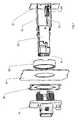
- Fig. 1is shown in an exploded view of a typical installation situation of a connector socket according to the invention.
- the socketis installed in a device from which in Fig. 1 only a section of the device wall 10 is shown.
- a device circuit board 12 z. B.installed parallel to the device wall 10.
- the connector socketis positioned on the one hand in a breakthrough of the device wall 10 and on the other hand electrically connected to the device circuit board 12.
- the connector socket 14is formed in the illustrated embodiment as an RJ socket.
- a protective housing 16is inserted in the wall opening of the device wall 10 in a conventional manner, which is sealed by a seal 18 against the device wall 10 and screwed by a nut 20 with the device wall 10 is.
- the connector socket 14is inserted in the illustrated embodiment of the device interior in the protective housing 16 and fixed there exact position. Also an insertion from the outside conceivable.
- the protective housing 16is used to attach a connector housing which encloses the plug-in connector 14 to be inserted into the connector plug. Since the plug housing is fitted accurately and sealed onto the protective housing 16, an exact positioning of the socket 14 in the protective housing 16 is necessary.
- the exact positioning of the socket 14 in the protective housing 16 and thus in the device wall 10has the consequence that dimensional tolerances affect the installation of the device circuit board 12 with respect to the device wall 10 on the connection of the socket 14 to the device circuit board 12.
- These position tolerancesare compensated according to the invention in that the connector socket 14 is arranged in a socket housing 22 and is connected to a printed circuit board 24, which is also arranged fixed in position in the socket housing 22.
- the printed circuit board 24protrudes from the socket housing 22 at the end facing away from the socket 14. At the free edge of the printed circuit board 24 protruding from the socket housing 22, opposite the socket 14, printed circuit board edge plug contacts 26 are formed.
- edge plug contacts 26is the Printed circuit board 24 is inserted into a printed circuit board edge connector socket 28 which is arranged on the device circuit board 12.
- the plug-in direction of the printed circuit board 24 with its edge plug contacts 26 in the edge connector socket 28coincides with the plug-in direction of the connector socket 14.
- the contact length of the edge plug contacts 26 and the edge socket 28 in the insertionallows for a tolerance in the insertion of the circuit board 24 in the edge connector 28 and thus a distance tolerance between the fixed in the protective housing 16 and the device wall 10 connector socket 14 and in the device built-in device board 12. Even in the direction perpendicular to the plug axis, ie in the plane of the device board 12, low installation tolerances can be compensated.
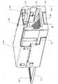
- the structure of the female housing 22will be described below with reference to FIGS. 2 to 4 explained.
- the socket housing 22has a front part 30, which preferably consists of metal and in particular of zinc die casting.
- the front part 30forms the receiving space for the male connector 14 to be inserted into the connector plug. Due to the metallic material, the front part 30 also forms a shield of the connector. Outside on the side walls of the front part 30 locking grooves 32 are formed, which serve for securing the front part 30 and thus the entire female housing 22 in the protective housing 16.
- the front part 30is followed by an insulating body 34 made of plastic.
- the insulating body 34is attached from the rear to the front part 30 and closes with its front end wall, the back of the front part 30.
- a protruding over this front end wall base plate of the insulating body 34forms the bottom of the receiving space of the front part 30.
- guide slots 36are formed, which serve to receive the socket contacts 38.
- the socket contacts 38are arranged in the manner known for RJ sockets and resilient. The socket contacts 38 engage through the guide slots 36 in the receiving space of the socket and are insulated by the insulating body 34.
- the circuit board 24is inserted from the rear and fixed to the bottom side in the insulating body 34.
- the printed circuit board 24carries on its front edge inserted into the insulating body 34, the female contacts 38.
- the female contacts 38are connected to the edge connector contacts 26, which are arranged on the opposite rear edge of the printed circuit board 24. Since the printed circuit board 24 is parallel to the bottom of the insulating body 34, the plugging direction of the socket 14 with the socket contacts 38 in the same direction as the plugging direction of the edge plug contacts 26 runs.
- the insulating body 34is enclosed by a shroud jacket 40.
- the shroud jacket 40abuts the four side surfaces of the insulating body 34 and closes the rear surface of the insulating body 34 facing away from the socket 14 except for an entry slot for the printed circuit board 24.
- In the bottom 42 of the insulating body 34is in the area in which the Circuit board 24 adjacent to the bottom 42, an opening 44 recessed, through which a from the shroud jacket 40 inwardly bent contact spring 46 engages to contact a corresponding conductor track of the circuit board 24.
- the contact spring 46can be soldered to this conductor.
- the shroud jacket 40extends beyond the insulation body 34 and over the front part 30.
- the connector between the socket 14 and a plugged into this plugis thus completely shielded by the front part 30 and the shroud jacket 40.
- the shieldis also passed over the contact spring 46 to the circuit board 24.
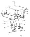
- the assembly of the female housing 22is based on the FIGS. 5 to 8 explained in more detail.
- FIG. 5shows in a detailed view of the circuit board 24. It can be seen that in this embodiment, the resilient socket contacts 38 are embedded in a support member 58 manufactured as an injection molded part, whereby their exact positioning is facilitated. The support member 58 is attached to the front end edge of the circuit board 24 to connect the socket contacts 38 with the tracks of the circuit board 24 and to solder.
- FIG. 5shows that on the circuit board 24 even more electronic circuit components 60 can be arranged and interconnected. These may be, for example, transformers, capacitors, resistors and the like, which are then preferably also received in the insulating body 34 and shielded by the shroud coat 40. Such electronic components are used, for example, to adapt the interface to the transmission path of the data network.
- FIG. 6shows in an individual view the insulating body 34.
- the insulating body 34is made as a one-piece plastic injection-molded part.
- the bottom 42can be swiveled downwards in the rear region, for which purpose the bottom 42 is connected to the remaining insulation body 34 via a film hinge 62.
- Insulating body 34is produced by injection molding with base 42 pivoted downwards at right angles. This arrangement of the bottom 42 allows a undercut-free design of the injection molding tools.
- the bottom 42remains in the assembly initially in the downwardly pivoted position, as in FIG. 7 is shown.
- the circuit board 24is used, wherein the support member 58 is inserted into a molded under the guide slots 36 and in front of the film hinge 62 in the insulating body 34 bottom pocket 72 and the circuit board 24 is guided in grooves 66, the inside of the side walls of the insulating body 34 are formed.
- the socket contacts 38pass through the guide slots 36, as shown in FIG FIG. 8 is shown.
- the bottom 42is pivoted up, so that it applies from below to the circuit board 24.
- the bottom 42has at its two free rear corners each upwardly directed corner projections 64 which engage around the circuit board 24 formed corners, so that the circuit board 24 is fixed against displacement in its plane.
- the circuit board 24is fixed in the insulating body 34 against movement perpendicular to the plane of the circuit board.
- the bottom 42is locked in the insulating body 34.
- molded resilient locking lugs 68which engage in lateral recesses of the circuit board 24 and engage behind latching edges 70 which are integrally formed on the side walls of the insulating body 34.
Landscapes
- Engineering & Computer Science (AREA)
- Microelectronics & Electronic Packaging (AREA)
- Details Of Connecting Devices For Male And Female Coupling (AREA)
- Coupling Device And Connection With Printed Circuit (AREA)
Description
Translated fromGermanDie Erfindung betrifft eine Steckverbinder-Buchse für die Daten und Kommunikationstechnik gemäss dem Oberbegriff des Patentanspruchs 1.The invention relates to a connector socket for the data and communication technology according to the preamble of patent claim 1.
In der Daten- und Kommunikationstechnik werden Steckverbinder-Buchsen als Schnittstelle eingesetzt, wobei diese Buchsen heute in der Regel standardisierte RJ-Buchsen sind. Diese Buchsen werden häufig direkt auf eine Leiterplatte gelötet, um eine kostengünstige Verschaltung zu ermöglichen. Ist die Buchse in Folge eines häufigen Steckens einem starken Verschleiß ausgesetzt, so ist das Austauschen der Buchse aufwändig. Ein weiteres Problem ergibt sich bei dem Einsatz in rauer Industrieumgebung, z. B. in Verbindung mit Industrial Ethernet, wenn die Buchsen mit einem zusätzlichen Schutzgehäuse versehen werden. Da die Positionierung der Buchsen in dem Schutzgehäuse sehr präzise erfolgen muss, kann es zu Toleranzproblemen kommen, wenn die Buchse direkt mit der Leiterplatte für die Elektronik verbunden ist.In data and communication technology, connector sockets are used as an interface, whereby these sockets are today generally standardized RJ sockets. These jacks are often soldered directly to a printed circuit board to allow a cost-effective interconnection. If the socket is subject to heavy wear as a result of frequent insertion, replacement of the socket is complicated. Another problem arises when used in harsh industrial environment, z. Eg in connection with Industrial Ethernet, if the sockets are provided with an additional protective housing. Since the positioning of the sockets in the protective housing must be very precise, tolerance problems can arise if the socket is connected directly to the printed circuit board for the electronics.
Aus der
Der Erfindung liegt die Aufgabe zugrunde, eine Steckverbinder-Buchse für die Daten- und Kommunikationstechnik zur Verfügung zu stellen, die Positionstoleranzen zwischen der positioniert in eine Gerätewand eingebauten Buchse und einer Geräte-Leiterplatte, mit welcher diese Buchse verbunden ist, ausgleichen kann und ein einfaches Austauschen der Buchse ermöglicht.The invention has for its object to provide a connector socket for the data and communication available, the position tolerances between the positioned in a device wall built-in jack and a device board, with which this socket is connected, can compensate and a simple Replacing the socket allows.
Diese Aufgabe wird erfindungsgemäß gelöst durch eine Steckverbinder-Buchse mit den Merkmalen des Patentanspruchs 1.This object is achieved by a connector socket with the features of claim 1.
Vorteilhafte Ausführungen der Erfindung sind in den Unteransprüchen angegeben.Advantageous embodiments of the invention are specified in the subclaims.
Mit dem Begriff "Steckverbinder-Buchse" oder kurz "Buchse" werden im Rahmen der Erfindung alle Buchsen von Steckverbinder-Systemen bezeichnet, die in der Daten- und Kommunikationstechnik als trennbare Schnittstellen verwendet werden. Als aktuelle Ausführung sind dies insbesondere RJ-Buchsen, z. B. RJ45-Buchsen.In the context of the invention, the term "connector socket" or "socket" for short designates all sockets of connector systems which are used in data and communication technology as separable interfaces. As current version, these are in particular RJ sockets, z. B. RJ45 sockets.
Unter "Geräten", in deren Gerätewand die Steckverbinder-Buchse positionierbar ist und mit deren Geräte-Leiterplatte die Buchse elektrisch leitend verbunden wird, werden im Rahmen der Erfindung alle Einrichtungen verstanden, an welche über die Steckverbinder-Buchse ein Daten- oder Kommunikationskabel anschließbar ist. Solche Geräte können Sende- und Empfangsgeräte sein und ebenso Anschlussdosen oder dergleichen.Under "devices", in the device wall, the connector socket is positioned and connected to the device board the socket electrically conductive, are understood in the context of the invention, all devices to which a data or communication cable can be connected via the connector socket , Such devices may be transmitting and receiving devices and also junction boxes or the like.
Erfindungsgemäß ist die Steckverbinder-Buchse in einem Buchsengehäuse angeordnet und an eine ebenfalls in diesem Buchsengehäuse angeordnete Leiterplatte angeschlossen. Die Leiterplatte weist an ihrem von der Buchse abgewandten Rand Leiterplatten-Randsteckerkontakte auf und wird mit diesen Randsteckerkontakten in eine Leitezplatten-Randsteckerbuchse der Geräte-Leiterplatte eingesteckt. Die Buchse ist somit über die Leiterplatte und die Randsteckerverbindung unmittelbar mit der Geräte-Leiterplatte elektrisch verbunden und verschaltet. Die steckbare Randsteckerverbindung zwischen der Leiterplatte und Geräte-Leiterplatte erlaubt dabei ein einfaches Austauschen der Buchse, da keine feste Lötverbindung zwischen der Buchse und der Geräte-Leiterplatte vorhanden ist. Außerdem weist die Randsteckerverbindung zwischen der Leiterplatte der Buchse und der Geräte-Leiterplatte eine mechanische Positionstoleranz in der Einsteckrichtung dieser Randsteckerverbindung auf, wodurch sich Positionstoleranzen zwischen der Einbauposition der Buchse und der Einbauposition der Geräte-Leiterplatte ausgleichen lassen. Auch geringe Positionstoleranzen in den zur Einsteckrichtung senkrechten Achsen können ausgeglichen werden.According to the connector socket is arranged in a socket housing and connected to a likewise arranged in this socket housing circuit board. The circuit board has on its edge facing away from the socket PCB edge plug contacts and is with these edge plug contacts plugged into a Leitezplatten edge connector socket of the device board. The socket is thus electrically connected via the circuit board and the edge connector directly to the device circuit board and interconnected. The pluggable edge connector between the circuit board and device board allows a simple replacement of the socket, since there is no fixed solder joint between the socket and the device circuit board. In addition, the edge plug connection between the printed circuit board of the socket and the device circuit board on a mechanical position tolerance in the insertion of this edge connector, whereby positional tolerances between the installation position of the socket and the installation position of the device circuit board can be compensated. Even small positional tolerances in the axes perpendicular to the plug-in direction can be compensated.
Erfindungsgemäß ist ferner das Buchsengehäuse von einem Schirmblech-Mantel umschlossen, wobei die Leiterplatten-Randsteckerbuchse von einem mit der Geräte-Leiterplatte verbundenen Schirmblech umschlossen ist, welches den Schirmblech-Mantel des in die Leiterplatten-Randsteckerbuchse eingesteckten Buchsengehäuses kontaktiert.According to the invention, the socket housing is further enclosed by a shroud jacket, wherein the circuit board edge connector socket is enclosed by a connected to the device circuit board shield plate, which contacts the shroud jacket of the plugged into the PCB edge connector socket jack housing.
Vorteilhaft ist es, dass auf der Leiterplatte der Buchse auch noch zusätzliche elektronische Komponenten zur Verschaltung der Buchse angeordnet werden können. Bspw. können Filter und/oder Transformatoren auf der Leiterplatte angeordnet werden, wie sie z. B. zur Anpassung der Schnittstelle für Ethernet benötigt werden.It is advantageous that additional electronic components for interconnecting the socket can also be arranged on the printed circuit board of the socket. For example. filters and / or transformers can be arranged on the circuit board, as z. B. to adapt the interface for Ethernet needed.
Das Buchsengehäuse weist in einer vorteilhaften Ausführung ein Vorderteil und einen sich daran anschließenden Isolationskörper auf. Das Vorderteil besteht vorzugsweise aus Metall, insbesondere aus Zinkdruckguss. Der Isolationskörper nimmt die Buchsenkontakte auf. Das metallische Vorderteil und ein den Isolationskörper umschließender Schirmblech-Mantel bilden eine Schirmung der gesamten Buchse. Das metallische Vorderteil begünstigt dabei eine genaue Montage der Buchse in einem Schutzgehäuse, wie dies für den Einsatz in Industrieumgebung gefordert wird.The female housing in an advantageous embodiment, a front part and an adjoining insulating body. The front part is preferably made of metal, in particular die-cast zinc. The insulating body takes the socket contacts on. The metallic front part and the insulating body surrounding shroud jacket form a shield of the entire socket. The metallic front part favors a precise mounting of the socket in a protective housing, as required for use in industrial environments.
Eine vorteilhafte Herstellung und Montage ergibt sich in einer Ausführung, wenn der Isolationskörper mit einem abschwenkbaren Boden ausgebildet ist. Die Leiterplatte kann vollständig hergestellt und montiert werden, d. h. mit den Buchsenkontakten, den Randsteckerkontakten und den eventuell erforderlichen zusätzlichen Schaltungsbauteilen bestückt werden und wird dann komplett montiert in den Isolationskörper eingesetzt und durch Hochschwenken des Bodens lagegenau in dem Isolationskörper fixiert. Dabei ist es für die Herstellung von besonderem Vorteil, wenn der Isolationskörper mit dem Boden als einstückiges Kunststoff-Spritzgussteil hergestellt wird, wobei der Boden mit dem Isolationskörper über ein Filmscharnier schwenkbar verbunden ist.An advantageous production and assembly results in an embodiment, when the insulating body is formed with a swing-bottom. The printed circuit board can be completely manufactured and assembled, ie equipped with the socket contacts, the edge plug contacts and any additional circuit components required and is then fully assembled in the insulation body and fixed by pivoting the soil in the exact position in the insulation body. It is for the production of particular advantage, when the insulating body with the ground as a one-piece Plastic injection molded part is produced, wherein the bottom is pivotally connected to the insulating body via a film hinge.
Im Folgenden wird die Erfindung anhand eines in der Zeichnung dargestellten Ausführungsbeispieles näher erläutert. Es zeigen
- Fig. 1
- in einer Explosionsdarstellung den Einbau der Buchse in ein Gehäuse,
- Fig. 2
- die Buchse in einer isometrischen Ansicht,
- Fig. 3
- die Buchse in einer Explosionsdarstellung,
- Fig. 4
- einen Axialschnitt durch die Buchse,
- Fig. 5
- die montierte Leiterplatte der Buchse,
- Fig. 6
- in einer Einzeldarstellung den Isolationskörper,
- Fig. 7
- das Einsetzen der Leiterplatte in den Isolationskörper und
- Fig. 8
- das Fixieren der Leiterplatte in dem Isolationskörper in einer aufgeschnittenen Ansicht.
- Fig. 1
- in an exploded view, the installation of the socket in a housing,
- Fig. 2
- the socket in an isometric view,
- Fig. 3
- the socket in an exploded view,
- Fig. 4
- an axial section through the socket,
- Fig. 5
- the assembled circuit board of the socket,
- Fig. 6
- in a detail representation of the insulating body,
- Fig. 7
- the insertion of the circuit board in the insulation body and
- Fig. 8
- fixing the printed circuit board in the insulating body in a cutaway view.
In
Um die Buchse 14 in einer rauen Industrieumgebung einsetzen zu können, ist in dem Wanddurchbruch der Gerätewand 10 in an sich bekannter Weise ein Schutzgehäuse 16 eingesetzt, welches durch eine Dichtung 18 gegen die Gerätewand 10 abgedichtet ist und durch eine Mutter 20 mit der Gerätewand 10 verschraubt ist. Die Steckverbinder-Buchse 14 wird im dargestellten Ausführungsbeispiel vom Geräteinneren in das Schutzgehäuse 16 eingesetzt und dort positionsgenau fixiert. Auch ein Einschieben von außen denkbar. Das Schutzgehäuse 16 dient zum Aufstecken eines Steckergehäuses, welches den in die Steckverbinder-Buchse 14 einzusteckenden Steckverbinder-Stecker umschließt. Da das Steckergehäuse passgenau und abgedichtet auf das Schutzgehäuse 16 aufgesteckt wird, ist eine exakte Positionierung der Buchse 14 in dem Schutzgehäuse 16 notwendig.In order to use the
Die exakte Positionierung der Buchse 14 in dem Schutzgehäuse 16 und damit in der Gerätewand 10 hat zur Folge, dass sich Maßtoleranzen beim Einbau der Geräte-Leiterplatte 12 in Bezug auf die Gerätewand 10 auf das Anschließen der Buchse 14 an die Geräte-Leiterplatte 12 auswirken. Diese Positionstoleranzen werden erfindungsgemäß dadurch ausgeglichen, dass die Steckverbinder-Buchse 14 in einem Buchsengehäuse 22 angeordnet ist und an eine Leiterplatte 24 angeschlossen ist, die ebenfalls lagefest in dem Buchsengehäuse 22 angeordnet ist. Die Leiterplatte 24 ragt an dem von der Buchse 14 abgewandten Ende aus dem Buchsengehäuse 22. An dem aus dem Buchsengehäuse 22 ragenden, der Buchse 14 entgegengesetzten freien Rand der Leiterplatte 24 sind Leiterplatten-Randsteckerkontakte 26 ausgebildet. Mit diesen Leiterplatten-Randsteckerkontakten 26 wird die Leiterplatte 24 in eine Leiterplatten-Randsteckerbuchse 28 eingesteckt, die an der Geräte-Leiterplatte 12 angeordnet ist. Die Einsteckrichtung der Leiterplatte 24 mit ihren Randsteckerkontakten 26 in die Randsteckerbuchse 28 stimmt dabei mit der Steckrichtung der Steckverbinder-Buchse 14 überein. Die Kontaktlänge der Randsteckerkontakte 26 und der Randsteckerbuchse 28 in der Einsteckrichtung lässt eine Toleranz in dem Einsteckweg der Leiterplatte 24 in die Randsteckerbuchse 28 zu und somit eine Abstandstoleranz zwischen der in dem Schutzgehäuse 16 und der Gerätewand 10 festgelegten Steckverbinder-Buchse 14 und der in dem Gerät eingebauten Geräte-Leiterplatte 12. Auch in den zu der Einsteckrichtung senkrechten Achsen, d. h. in der Ebene der Geräte-Leiterplatte 12, können geringe Einbautoleranzen ausgeglichen werden.The exact positioning of the
Der Aufbau des Buchsengehäuses 22 wird nachfolgend anhand der
Das Buchsengehäuse 22 weist ein Vorderteil 30 auf, welches vorzugsweise aus Metall und insbesondere aus Zinkdruckguss besteht. Das Vorderteil 30 bildet den Aufnahmeraum für den in die Steckverbinder-Buchse 14 einzusteckenden Steckverbinder-Stecker. Aufgrund des metallischen Werkstoffes bildet das Vorderteil 30 auch eine Schirmung der Steckverbindung. Außen an den Seitenwänden des Vorderteils 30 sind Rastnuten 32 eingeformt, die zum Befestigen des Vorderteils 30 und damit des gesamten Buchsengehäuses 22 in dem Schutzgehäuse 16 dienen.The
An das Vorderteil 30 schließt sich ein Isolationskörper 34 aus Kunststoff an. Der Isolationskörper 34 wird von hinten an das Vorderteil 30 angesetzt und verschließt mit seiner vorderen Stirnwand die Rückseite des Vorderteils 30. Eine über diese vordere Stirnwand vorspringende Bodenplatte des Isolationskörpers 34 bildet den Boden des Aufnahmeraumes des Vorderteiles 30. In der Stirnwand und der Bodenplatte des Isolationskörpers 34 sind Führungsschlitze 36 ausgebildet, die zur Aufnahme der Buchsenkontakte 38 dienen. Die Buchsenkontakte 38 sind in der für RJ-Buchsen bekannten Weise angeordnet und federnd ausgebildet. Die Buchsenkontakte 38 greifen durch die Führungsschlitze 36 in den Aufnahmeraum der Buchse und sind durch den Isolationskörper 34 isoliert.The
In den Isolationskörper 34 wird von hinten die Leiterplatte 24 eingesetzt und bodenseitig in dem Isolationskörper 34 fixiert. Die Leiterplatte 24 trägt an ihrem vorderen in den Isolationskörper 34 eingesetzten Rand die Buchsenkontakte 38. Über Leiterbahnen der Leiterplatte 24 sind die Buchsenkontakte 38 mit den Randsteckerkontakten 26 verschaltet, die am entgegengesetzten hinteren Rand der Leiterplatte 24 angeordnet sind. Da die Leiterplatte 24 parallel zum Boden des Isolationskörpers 34 liegt, verläuft die Steckrichtung der Buchse 14 mit den Buchsenkontakten 38 in derselben Richtung wie die Steckrichtung der Randsteckerkontakte 26.In the insulating
Der Isolationskörper 34 wird von einem Schirmblech-Mantel 40 umschlossen. Der Schirmblech-Mantel 40 liegt an den vier Seitenflächen des Isolationskörpers 34 an und verschließt die von der Buchse 14 abgewandte Rückfläche des Isolationskörpers 34 bis auf einen Eintrittsschlitz für die Leiterplatte 24. In dem Boden 42 des Isolationskörpers 34 ist in dem Bereich, in welchem die Leiterplatte 24 an den Boden 42 angrenzt, eine Öffnung 44 ausgespart, durch welche eine aus dem Schirmblech-Mantel 40 nach innen gebogene Kontaktfeder 46 hindurchgreift, um eine entsprechende Leiterbahn der Leiterplatte 24 zu kontaktieren. Gegebenenfalls kann die Kontaktfeder 46 mit dieser Leiterbahn verlötet werden. An der Oberseite und an der Unterseite greift der Schirmblech-Mantel 40 über den Isolationskörper 34 hinaus und über das Vorderteil 30. Mit nach innen abgewinkelten Ecken 48 der oberen Vorderkante und mit einem nach innen abgewinkelten Rand 50 der unteren Vorderkante greift der Schirmblech-Mantel 40 vor die Stirnfläche des Vorderteils 30, wodurch der Schirmblech-Mantel 40 das Vorderteil 30 und den Isolationskörper 34 in der montierten Stellung zusammenhält und aneinander fixiert. An den Seitenwänden des SchirmblechMantels 40 sind nach vorn gerichtete Federzungen 52 ausgebildet, die nach innen abgekröpft sind und durch Schlitze der Stirnwand des Isolationskörpers 34 hindurch in den Aufnahmeraum der Buchse 14 greifen. Die Federzungen 52 kontaktieren die Schirmung eines in die Buchse 14 eingesteckten Steckers. Weiter sind an den seitlichen Rändern der nach vorne ragenden Unterseite des Schirmblechmantels 40 Kontaktfedern 56 ausgebildet, die in Nuten des Vorderteils 30 liegen und über dessen Außenfläche ausgewölbt sind, um gegebenenfalls ein metallisches Schutzgehäuse oder dergleichen zu Kontaktieren.The insulating
Wird das Buchsengehäuse 22 mit der Leiterplatte 24 und deren Randsteckerkontakten 26 in die Randsteckerbuchse 28 der Geräte-Leiterplatte 12 eingesteckt, wie dies in
Die Steckverbindung zwischen der Buchse 14 und einem in diese eingesteckten Stecker ist somit durch das Vorderteil 30 und den Schirmblech-Mantel 40 vollständig abgeschirmt. Dabei wird die Schirmung des eingesteckten Steckers insbesondere über die Federzungen 52 an den Schirmblech-Mantel 40 übergeben. Die Schirmung wird außerdem über die Kontaktfeder 46 an die Leiterplatte 24 übergeben wird.The connector between the
Die Montage des Buchsengehäuses 22 wird anhand der
Der Boden 42 bleibt bei der Montage zunächst in der nach unten abgeschwenkten Stellung, wie dies in
- 1010
- Gerätewanddevice wall
- 1212
- Geräte-LeiterplatteDevice PCB
- 1414
- Steckverbinder-BuchseConnector socket
- 1616
- Schutzgehäusehousing
- 1818
- Dichtungpoetry
- 2020
- Muttermother
- 2222
- Buchsengehäusesocket housing
- 2424
- Leiterplattecircuit board
- 2626
- RandsteckerkontakteEdge connector contacts
- 2828
- RandsteckerbuchseEdge connector socket
- 3030
- Vorderteilfront
- 3232
- Rastnutenlocking grooves
- 3434
- Isolationskörperinsulation body
- 3636
- Führungsschlitzeguide slots
- 3838
- Buchsenkontaktefemale contacts
- 4040
- Schirmblech-MantelShroud jacket
- 4242
- Bodenground
- 4444
- Öffnungopening
- 4646
- Kontaktfedercontact spring
- 4848
- Eckencorners
- 5050
- Randedge
- 5252
- Federzungenspring tongues
- 5454
- Schirmblechshroud
- 5656
- Kontaktfederncontact springs
- 5858
- Trägerelementsupport element
- 6060
- Schaltungsbauteilecircuit components
- 6262
- Filmscharnierfilm hinge
- 6464
- Eckvorsprüngecorner projections
- 6666
- Nutengroove
- 6868
- Rastnasenlocking lugs
- 7070
- Rastkantecatch edge
- 7272
- Bodentaschebottom pocket
Claims (7)
- A plug connector socket for data and communications technology, which is capable of being positioned in a wall (10) of an appliance and is capable of being connected in an electrically conductive manner to a circuit board (12) of the appliance, wherein the socket (14) is arranged stationary in a socket casing (22) which has a front part (30) and an insulation body (34) receiving socket contacts (38), a circuit board (24) which is capable of being inserted in the insulation body (34) and of being fixed in the latter is arranged stationary in the socket casing (22), the plane of the circuit board (24) is situated parallel to the insertion direction of the socket (14), the contacts (38) of the socket (14) are connected to the circuit board (24) in a conductive manner, and at its edge facing away from the socket (14) the circuit board (24) has circuit board edge connector contacts (26) for insertion into a circuit board edge connector socket (28) of the circuit board (12) of the appliance,characterized in that the socket casing (22) is surrounded by a shield plate jacket (40), the circuit board edge connector socket (28) is surrounded by a shield plate (54) which is connected to the circuit board (12) of the appliance and which contacts the shield plate jacket (40) of the socket casing (22) inserted into the circuit board edge connector socket (28).
- A plug connector socket according to claim 1,characterized in that the socket casing (22) is capable of being positioned in a protective casing (16) attached to the wall (10) of the appliance.
- A plug connector socket according to claim 1 or 2,characterized in that the front part (30) consists of metal, and in particular of die-cast zinc.
- A plug connector socket according to claim 3,characterized in that the shield plate jacket (40) contacts the front part (30) in an electrically conductive manner.
- A plug connector socket according to claim 1 or 2,characterized in that the insulation body (34) has a pivotable base (42), and, when the base (42) is pivoted down, the circuit board (24) is capable of being inserted into the insulation body (34) and is fixed in position in the insulation body (34) by the base (42) pivoted down.
- A plug connector socket according to claim 5,characterized in that the insulation body (34) is produced in the form of a plastics material injection-moulded part in one piece with the base (42), and the base (42) is joined to the insulation body (34) by way of a film hinge (62).
- A plug connector socket according to any one of the preceding claims,characterized in that the circuit board (24) carries additional electrical circuit components (60) which are connected to the socket (14) by way of the circuit board (24).
Applications Claiming Priority (2)
| Application Number | Priority Date | Filing Date | Title |
|---|---|---|---|
| DE102008050111ADE102008050111B3 (en) | 2008-10-06 | 2008-10-06 | Connector socket arrangement for data and communication technology |
| PCT/EP2009/006943WO2010040455A2 (en) | 2008-10-06 | 2009-09-25 | Plug connector socket for data and communication technology |
Publications (2)
| Publication Number | Publication Date |
|---|---|
| EP2332221A2 EP2332221A2 (en) | 2011-06-15 |
| EP2332221B1true EP2332221B1 (en) | 2012-11-14 |
Family
ID=42063270
Family Applications (1)
| Application Number | Title | Priority Date | Filing Date |
|---|---|---|---|
| EP09778730ANot-in-forceEP2332221B1 (en) | 2008-10-06 | 2009-09-25 | Plug connector socket for data and communication technology |
Country Status (3)
| Country | Link |
|---|---|
| EP (1) | EP2332221B1 (en) |
| DE (1) | DE102008050111B3 (en) |
| WO (1) | WO2010040455A2 (en) |
Cited By (56)
| Publication number | Priority date | Publication date | Assignee | Title |
|---|---|---|---|---|
| US10123706B2 (en) | 2016-07-27 | 2018-11-13 | Align Technology, Inc. | Intraoral scanner with dental diagnostics capabilities |
| US10130445B2 (en) | 2014-09-19 | 2018-11-20 | Align Technology, Inc. | Arch expanding appliance |
| US10248883B2 (en) | 2015-08-20 | 2019-04-02 | Align Technology, Inc. | Photograph-based assessment of dental treatments and procedures |
| US10327872B2 (en) | 2014-08-15 | 2019-06-25 | Align Technology, Inc. | Field curvature model for confocal imaging apparatus with curved focal surface |
| US10383705B2 (en) | 2016-06-17 | 2019-08-20 | Align Technology, Inc. | Orthodontic appliance performance monitor |
| US10390913B2 (en) | 2018-01-26 | 2019-08-27 | Align Technology, Inc. | Diagnostic intraoral scanning |
| US10421152B2 (en) | 2011-09-21 | 2019-09-24 | Align Technology, Inc. | Laser cutting |
| US10449016B2 (en) | 2014-09-19 | 2019-10-22 | Align Technology, Inc. | Arch adjustment appliance |
| US10456043B2 (en) | 2017-01-12 | 2019-10-29 | Align Technology, Inc. | Compact confocal dental scanning apparatus |
| US10470847B2 (en) | 2016-06-17 | 2019-11-12 | Align Technology, Inc. | Intraoral appliances with sensing |
| US10504386B2 (en) | 2015-01-27 | 2019-12-10 | Align Technology, Inc. | Training method and system for oral-cavity-imaging-and-modeling equipment |
| US10507087B2 (en) | 2016-07-27 | 2019-12-17 | Align Technology, Inc. | Methods and apparatuses for forming a three-dimensional volumetric model of a subject's teeth |
| US10517482B2 (en) | 2017-07-27 | 2019-12-31 | Align Technology, Inc. | Optical coherence tomography for orthodontic aligners |
| US10524881B2 (en) | 2010-04-30 | 2020-01-07 | Align Technology, Inc. | Patterned dental positioning appliance |
| US10537405B2 (en) | 2014-11-13 | 2020-01-21 | Align Technology, Inc. | Dental appliance with cavity for an unerupted or erupting tooth |
| US10548700B2 (en) | 2016-12-16 | 2020-02-04 | Align Technology, Inc. | Dental appliance etch template |
| US10595966B2 (en) | 2016-11-04 | 2020-03-24 | Align Technology, Inc. | Methods and apparatuses for dental images |
| US10610332B2 (en) | 2012-05-22 | 2020-04-07 | Align Technology, Inc. | Adjustment of tooth position in a virtual dental model |
| US10613515B2 (en) | 2017-03-31 | 2020-04-07 | Align Technology, Inc. | Orthodontic appliances including at least partially un-erupted teeth and method of forming them |
| US10639134B2 (en) | 2017-06-26 | 2020-05-05 | Align Technology, Inc. | Biosensor performance indicator for intraoral appliances |
| US10772506B2 (en) | 2014-07-07 | 2020-09-15 | Align Technology, Inc. | Apparatus for dental confocal imaging |
| US10779718B2 (en) | 2017-02-13 | 2020-09-22 | Align Technology, Inc. | Cheek retractor and mobile device holder |
| US10813720B2 (en) | 2017-10-05 | 2020-10-27 | Align Technology, Inc. | Interproximal reduction templates |
| US10885521B2 (en) | 2017-07-17 | 2021-01-05 | Align Technology, Inc. | Method and apparatuses for interactive ordering of dental aligners |
| US10893918B2 (en) | 2012-03-01 | 2021-01-19 | Align Technology, Inc. | Determining a dental treatment difficulty |
| US10919209B2 (en) | 2009-08-13 | 2021-02-16 | Align Technology, Inc. | Method of forming a dental appliance |
| US10980613B2 (en) | 2017-12-29 | 2021-04-20 | Align Technology, Inc. | Augmented reality enhancements for dental practitioners |
| US10993783B2 (en) | 2016-12-02 | 2021-05-04 | Align Technology, Inc. | Methods and apparatuses for customizing a rapid palatal expander |
| US11026831B2 (en) | 2016-12-02 | 2021-06-08 | Align Technology, Inc. | Dental appliance features for speech enhancement |
| US11045283B2 (en) | 2017-06-09 | 2021-06-29 | Align Technology, Inc. | Palatal expander with skeletal anchorage devices |
| US11083545B2 (en) | 2009-03-19 | 2021-08-10 | Align Technology, Inc. | Dental wire attachment |
| US11096763B2 (en) | 2017-11-01 | 2021-08-24 | Align Technology, Inc. | Automatic treatment planning |
| US11103330B2 (en) | 2015-12-09 | 2021-08-31 | Align Technology, Inc. | Dental attachment placement structure |
| US11116605B2 (en) | 2017-08-15 | 2021-09-14 | Align Technology, Inc. | Buccal corridor assessment and computation |
| US11123156B2 (en) | 2017-08-17 | 2021-09-21 | Align Technology, Inc. | Dental appliance compliance monitoring |
| US11219506B2 (en) | 2017-11-30 | 2022-01-11 | Align Technology, Inc. | Sensors for monitoring oral appliances |
| US11273011B2 (en) | 2016-12-02 | 2022-03-15 | Align Technology, Inc. | Palatal expanders and methods of expanding a palate |
| US11376101B2 (en) | 2016-12-02 | 2022-07-05 | Align Technology, Inc. | Force control, stop mechanism, regulating structure of removable arch adjustment appliance |
| US11419702B2 (en) | 2017-07-21 | 2022-08-23 | Align Technology, Inc. | Palatal contour anchorage |
| US11426259B2 (en) | 2012-02-02 | 2022-08-30 | Align Technology, Inc. | Identifying forces on a tooth |
| US11432908B2 (en) | 2017-12-15 | 2022-09-06 | Align Technology, Inc. | Closed loop adaptive orthodontic treatment methods and apparatuses |
| US11471252B2 (en) | 2008-10-08 | 2022-10-18 | Align Technology, Inc. | Dental positioning appliance having mesh portion |
| US11534974B2 (en) | 2017-11-17 | 2022-12-27 | Align Technology, Inc. | Customized fabrication of orthodontic retainers based on patient anatomy |
| US11534268B2 (en) | 2017-10-27 | 2022-12-27 | Align Technology, Inc. | Alternative bite adjustment structures |
| US11554000B2 (en) | 2015-11-12 | 2023-01-17 | Align Technology, Inc. | Dental attachment formation structure |
| US11564777B2 (en) | 2018-04-11 | 2023-01-31 | Align Technology, Inc. | Releasable palatal expanders |
| US11576752B2 (en) | 2017-10-31 | 2023-02-14 | Align Technology, Inc. | Dental appliance having selective occlusal loading and controlled intercuspation |
| US11596502B2 (en) | 2015-12-09 | 2023-03-07 | Align Technology, Inc. | Dental attachment placement structure |
| US11612454B2 (en) | 2010-04-30 | 2023-03-28 | Align Technology, Inc. | Individualized orthodontic treatment index |
| US11633268B2 (en) | 2017-07-27 | 2023-04-25 | Align Technology, Inc. | Tooth shading, transparency and glazing |
| US11931222B2 (en) | 2015-11-12 | 2024-03-19 | Align Technology, Inc. | Dental attachment formation structures |
| US11937991B2 (en) | 2018-03-27 | 2024-03-26 | Align Technology, Inc. | Dental attachment placement structure |
| US11996181B2 (en) | 2017-06-16 | 2024-05-28 | Align Technology, Inc. | Automatic detection of tooth type and eruption status |
| US12090020B2 (en) | 2017-03-27 | 2024-09-17 | Align Technology, Inc. | Apparatuses and methods assisting in dental therapies |
| US12171575B2 (en) | 2017-10-04 | 2024-12-24 | Align Technology, Inc. | Intraoral systems and methods for sampling soft-tissue |
| US12274597B2 (en) | 2017-08-11 | 2025-04-15 | Align Technology, Inc. | Dental attachment template tray systems |
Families Citing this family (2)
| Publication number | Priority date | Publication date | Assignee | Title |
|---|---|---|---|---|
| CN105048221A (en)* | 2015-06-28 | 2015-11-11 | 中航光电科技股份有限公司 | Equipment machine cabinet |
| JP6868596B2 (en)* | 2018-08-28 | 2021-05-12 | 矢崎総業株式会社 | Waterproof connector structure and connector fitting method of waterproof connector structure |
Family Cites Families (3)
| Publication number | Priority date | Publication date | Assignee | Title |
|---|---|---|---|---|
| US5947761A (en)* | 1998-09-29 | 1999-09-07 | The Whitaker Corporation | Electrical connector with pivoting wire fixture |
| US6848943B2 (en)* | 2002-04-16 | 2005-02-01 | Pulse Engineering, Inc. | Shielded connector assembly and method of manufacturing |
| US7387538B2 (en)* | 2006-03-23 | 2008-06-17 | Finisar Corporation | Connector structure for a transceiver module |
- 2008
- 2008-10-06DEDE102008050111Apatent/DE102008050111B3/ennot_activeExpired - Fee Related
- 2009
- 2009-09-25EPEP09778730Apatent/EP2332221B1/ennot_activeNot-in-force
- 2009-09-25WOPCT/EP2009/006943patent/WO2010040455A2/enactiveApplication Filing
Cited By (82)
| Publication number | Priority date | Publication date | Assignee | Title |
|---|---|---|---|---|
| US11471252B2 (en) | 2008-10-08 | 2022-10-18 | Align Technology, Inc. | Dental positioning appliance having mesh portion |
| US11083545B2 (en) | 2009-03-19 | 2021-08-10 | Align Technology, Inc. | Dental wire attachment |
| US10919209B2 (en) | 2009-08-13 | 2021-02-16 | Align Technology, Inc. | Method of forming a dental appliance |
| US11612454B2 (en) | 2010-04-30 | 2023-03-28 | Align Technology, Inc. | Individualized orthodontic treatment index |
| US10524881B2 (en) | 2010-04-30 | 2020-01-07 | Align Technology, Inc. | Patterned dental positioning appliance |
| US10828719B2 (en) | 2011-09-21 | 2020-11-10 | Align Technology, Inc. | Laser cutting |
| US10421152B2 (en) | 2011-09-21 | 2019-09-24 | Align Technology, Inc. | Laser cutting |
| US11426259B2 (en) | 2012-02-02 | 2022-08-30 | Align Technology, Inc. | Identifying forces on a tooth |
| US10893918B2 (en) | 2012-03-01 | 2021-01-19 | Align Technology, Inc. | Determining a dental treatment difficulty |
| US10610332B2 (en) | 2012-05-22 | 2020-04-07 | Align Technology, Inc. | Adjustment of tooth position in a virtual dental model |
| US10835128B2 (en) | 2014-07-07 | 2020-11-17 | Align Technology, Inc. | Apparatus for dental confocal imaging |
| US11369271B2 (en) | 2014-07-07 | 2022-06-28 | Align Technology, Inc. | Apparatus for dental imaging |
| US10772506B2 (en) | 2014-07-07 | 2020-09-15 | Align Technology, Inc. | Apparatus for dental confocal imaging |
| US10624720B1 (en) | 2014-08-15 | 2020-04-21 | Align Technology, Inc. | Imaging apparatus with temperature compensation |
| US10952827B2 (en) | 2014-08-15 | 2021-03-23 | Align Technology, Inc. | Calibration of an intraoral scanner |
| US10507089B2 (en) | 2014-08-15 | 2019-12-17 | Align Technology, Inc. | Imaging apparatus with simplified optical design |
| US10507088B2 (en) | 2014-08-15 | 2019-12-17 | Align Technology, Inc. | Imaging apparatus with simplified optical design |
| US10327872B2 (en) | 2014-08-15 | 2019-06-25 | Align Technology, Inc. | Field curvature model for confocal imaging apparatus with curved focal surface |
| US11638629B2 (en) | 2014-09-19 | 2023-05-02 | Align Technology, Inc. | Arch expanding appliance |
| US11744677B2 (en) | 2014-09-19 | 2023-09-05 | Align Technology, Inc. | Arch adjustment appliance |
| US10449016B2 (en) | 2014-09-19 | 2019-10-22 | Align Technology, Inc. | Arch adjustment appliance |
| US10130445B2 (en) | 2014-09-19 | 2018-11-20 | Align Technology, Inc. | Arch expanding appliance |
| US10537405B2 (en) | 2014-11-13 | 2020-01-21 | Align Technology, Inc. | Dental appliance with cavity for an unerupted or erupting tooth |
| US10504386B2 (en) | 2015-01-27 | 2019-12-10 | Align Technology, Inc. | Training method and system for oral-cavity-imaging-and-modeling equipment |
| US11037466B2 (en) | 2015-01-27 | 2021-06-15 | Align Technology, Inc. | Training method and system for oral-cavity-imaging-and-modeling equipment |
| US11042774B2 (en) | 2015-08-20 | 2021-06-22 | Align Technology, Inc. | Photograph-based assessment of dental treatments and procedures |
| US10248883B2 (en) | 2015-08-20 | 2019-04-02 | Align Technology, Inc. | Photograph-based assessment of dental treatments and procedures |
| US11931222B2 (en) | 2015-11-12 | 2024-03-19 | Align Technology, Inc. | Dental attachment formation structures |
| US11554000B2 (en) | 2015-11-12 | 2023-01-17 | Align Technology, Inc. | Dental attachment formation structure |
| US11596502B2 (en) | 2015-12-09 | 2023-03-07 | Align Technology, Inc. | Dental attachment placement structure |
| US11103330B2 (en) | 2015-12-09 | 2021-08-31 | Align Technology, Inc. | Dental attachment placement structure |
| US10470847B2 (en) | 2016-06-17 | 2019-11-12 | Align Technology, Inc. | Intraoral appliances with sensing |
| US11612455B2 (en) | 2016-06-17 | 2023-03-28 | Align Technology, Inc. | Orthodontic appliance performance monitor |
| US10888396B2 (en) | 2016-06-17 | 2021-01-12 | Align Technology, Inc. | Intraoral appliances with proximity and contact sensing |
| US10383705B2 (en) | 2016-06-17 | 2019-08-20 | Align Technology, Inc. | Orthodontic appliance performance monitor |
| US10606911B2 (en) | 2016-07-27 | 2020-03-31 | Align Technology, Inc. | Intraoral scanner with dental diagnostics capabilities |
| US10585958B2 (en) | 2016-07-27 | 2020-03-10 | Align Technology, Inc. | Intraoral scanner with dental diagnostics capabilities |
| US10528636B2 (en) | 2016-07-27 | 2020-01-07 | Align Technology, Inc. | Methods for dental diagnostics |
| US10888400B2 (en) | 2016-07-27 | 2021-01-12 | Align Technology, Inc. | Methods and apparatuses for forming a three-dimensional volumetric model of a subject's teeth |
| US10509838B2 (en) | 2016-07-27 | 2019-12-17 | Align Technology, Inc. | Methods and apparatuses for forming a three-dimensional volumetric model of a subject's teeth |
| US10507087B2 (en) | 2016-07-27 | 2019-12-17 | Align Technology, Inc. | Methods and apparatuses for forming a three-dimensional volumetric model of a subject's teeth |
| US10123706B2 (en) | 2016-07-27 | 2018-11-13 | Align Technology, Inc. | Intraoral scanner with dental diagnostics capabilities |
| US10380212B2 (en) | 2016-07-27 | 2019-08-13 | Align Technology, Inc. | Methods and apparatuses for forming a three-dimensional volumetric model of a subject's teeth |
| US10932885B2 (en) | 2016-11-04 | 2021-03-02 | Align Technology, Inc. | Methods and apparatuses for dental images |
| US10595966B2 (en) | 2016-11-04 | 2020-03-24 | Align Technology, Inc. | Methods and apparatuses for dental images |
| US11191617B2 (en) | 2016-11-04 | 2021-12-07 | Align Technology, Inc. | Methods and apparatuses for dental images |
| US10993783B2 (en) | 2016-12-02 | 2021-05-04 | Align Technology, Inc. | Methods and apparatuses for customizing a rapid palatal expander |
| US11026831B2 (en) | 2016-12-02 | 2021-06-08 | Align Technology, Inc. | Dental appliance features for speech enhancement |
| US11376101B2 (en) | 2016-12-02 | 2022-07-05 | Align Technology, Inc. | Force control, stop mechanism, regulating structure of removable arch adjustment appliance |
| US11273011B2 (en) | 2016-12-02 | 2022-03-15 | Align Technology, Inc. | Palatal expanders and methods of expanding a palate |
| US10548700B2 (en) | 2016-12-16 | 2020-02-04 | Align Technology, Inc. | Dental appliance etch template |
| US10456043B2 (en) | 2017-01-12 | 2019-10-29 | Align Technology, Inc. | Compact confocal dental scanning apparatus |
| US11712164B2 (en) | 2017-01-12 | 2023-08-01 | Align Technology, Inc. | Intraoral scanner with moveable opto-mechanical module |
| US10918286B2 (en) | 2017-01-12 | 2021-02-16 | Align Technology, Inc. | Compact confocal dental scanning apparatus |
| US10779718B2 (en) | 2017-02-13 | 2020-09-22 | Align Technology, Inc. | Cheek retractor and mobile device holder |
| US12090020B2 (en) | 2017-03-27 | 2024-09-17 | Align Technology, Inc. | Apparatuses and methods assisting in dental therapies |
| US10613515B2 (en) | 2017-03-31 | 2020-04-07 | Align Technology, Inc. | Orthodontic appliances including at least partially un-erupted teeth and method of forming them |
| US11045283B2 (en) | 2017-06-09 | 2021-06-29 | Align Technology, Inc. | Palatal expander with skeletal anchorage devices |
| US11996181B2 (en) | 2017-06-16 | 2024-05-28 | Align Technology, Inc. | Automatic detection of tooth type and eruption status |
| US10639134B2 (en) | 2017-06-26 | 2020-05-05 | Align Technology, Inc. | Biosensor performance indicator for intraoral appliances |
| US10885521B2 (en) | 2017-07-17 | 2021-01-05 | Align Technology, Inc. | Method and apparatuses for interactive ordering of dental aligners |
| US11419702B2 (en) | 2017-07-21 | 2022-08-23 | Align Technology, Inc. | Palatal contour anchorage |
| US10517482B2 (en) | 2017-07-27 | 2019-12-31 | Align Technology, Inc. | Optical coherence tomography for orthodontic aligners |
| US11633268B2 (en) | 2017-07-27 | 2023-04-25 | Align Technology, Inc. | Tooth shading, transparency and glazing |
| US10842380B2 (en) | 2017-07-27 | 2020-11-24 | Align Technology, Inc. | Methods and systems for imaging orthodontic aligners |
| US12274597B2 (en) | 2017-08-11 | 2025-04-15 | Align Technology, Inc. | Dental attachment template tray systems |
| US11116605B2 (en) | 2017-08-15 | 2021-09-14 | Align Technology, Inc. | Buccal corridor assessment and computation |
| US11123156B2 (en) | 2017-08-17 | 2021-09-21 | Align Technology, Inc. | Dental appliance compliance monitoring |
| US12171575B2 (en) | 2017-10-04 | 2024-12-24 | Align Technology, Inc. | Intraoral systems and methods for sampling soft-tissue |
| US10813720B2 (en) | 2017-10-05 | 2020-10-27 | Align Technology, Inc. | Interproximal reduction templates |
| US11534268B2 (en) | 2017-10-27 | 2022-12-27 | Align Technology, Inc. | Alternative bite adjustment structures |
| US11576752B2 (en) | 2017-10-31 | 2023-02-14 | Align Technology, Inc. | Dental appliance having selective occlusal loading and controlled intercuspation |
| US11096763B2 (en) | 2017-11-01 | 2021-08-24 | Align Technology, Inc. | Automatic treatment planning |
| US11534974B2 (en) | 2017-11-17 | 2022-12-27 | Align Technology, Inc. | Customized fabrication of orthodontic retainers based on patient anatomy |
| US11219506B2 (en) | 2017-11-30 | 2022-01-11 | Align Technology, Inc. | Sensors for monitoring oral appliances |
| US11432908B2 (en) | 2017-12-15 | 2022-09-06 | Align Technology, Inc. | Closed loop adaptive orthodontic treatment methods and apparatuses |
| US10980613B2 (en) | 2017-12-29 | 2021-04-20 | Align Technology, Inc. | Augmented reality enhancements for dental practitioners |
| US10813727B2 (en) | 2018-01-26 | 2020-10-27 | Align Technology, Inc. | Diagnostic intraoral tracking |
| US10390913B2 (en) | 2018-01-26 | 2019-08-27 | Align Technology, Inc. | Diagnostic intraoral scanning |
| US11013581B2 (en) | 2018-01-26 | 2021-05-25 | Align Technology, Inc. | Diagnostic intraoral methods and apparatuses |
| US11937991B2 (en) | 2018-03-27 | 2024-03-26 | Align Technology, Inc. | Dental attachment placement structure |
| US11564777B2 (en) | 2018-04-11 | 2023-01-31 | Align Technology, Inc. | Releasable palatal expanders |
Also Published As
| Publication number | Publication date |
|---|---|
| WO2010040455A3 (en) | 2010-07-22 |
| DE102008050111B3 (en) | 2010-05-06 |
| EP2332221A2 (en) | 2011-06-15 |
| WO2010040455A2 (en) | 2010-04-15 |
Similar Documents
| Publication | Publication Date | Title |
|---|---|---|
| EP2332221B1 (en) | Plug connector socket for data and communication technology | |
| EP1814202B1 (en) | Coupling device | |
| DE69214947T2 (en) | Modular plug socket | |
| DE68921165T2 (en) | Shielded low profile receptacle. | |
| DE4222452A1 (en) | SHIELDED CONNECTOR | |
| DE102009056517B4 (en) | Connector assembly with first and second connector and mating connector | |
| EP3613110B1 (en) | Assembly for a plug connector part with a contact insert and a grounding element | |
| DE8911648U1 (en) | Electrical connector | |
| DE10393763T5 (en) | Circuit board connector with integral dielectric cover | |
| EP0341535B1 (en) | Miniature connection plug for coaxial cables | |
| DE102005029686A1 (en) | Antenna and means for mounting the antenna on a vehicle and for connecting the antenna to one or more cables of a wiring harness laid in the vehicle | |
| EP1282345B1 (en) | Housing for board with electronic components in vehicle | |
| DE202018101278U1 (en) | Connector module for a modular industrial connector for transmitting high data rates | |
| DE102014012739B4 (en) | Electrical connector, connector element and use | |
| EP4500637A1 (en) | Grounding module which is to be received in a metal plug connector modular frame and which grounds same | |
| DE10249981B3 (en) | Electronic control device comprises interference signal diversion plate between control module circuit board and carrier rail or carrier plate | |
| EP1534055B1 (en) | Housing for an electrical device | |
| DE602004008094T2 (en) | ELECTRICAL CONNECTOR FOR A FLEXIBLE FLAT LEADER AND SWITCHING DEVICE | |
| WO2024240297A1 (en) | Retaining frame for a connector housing for an industrial connector | |
| EP1006624A2 (en) | Socket for electrical connections | |
| DE102018202939B4 (en) | Plug for receiving electrical cables | |
| DE102004029300A1 (en) | Coaxial plug connector is angled connector with contact element mounted in plug connector housing so as to rotate about central axis of inner conductor of counter plug connector | |
| DE102021124290A1 (en) | Electrical signal distribution device | |
| WO2025119422A1 (en) | Connector module for a modular industrial connector | |
| DE20305734U1 (en) | Adaptor to connect cables of different types to standard base for control unit of pneumatic valve set |
Legal Events
| Date | Code | Title | Description |
|---|---|---|---|
| PUAI | Public reference made under article 153(3) epc to a published international application that has entered the european phase | Free format text:ORIGINAL CODE: 0009012 | |
| 17P | Request for examination filed | Effective date:20110118 | |
| AK | Designated contracting states | Kind code of ref document:A2 Designated state(s):AT BE BG CH CY CZ DE DK EE ES FI FR GB GR HR HU IE IS IT LI LT LU LV MC MK MT NL NO PL PT RO SE SI SK SM TR | |
| AX | Request for extension of the european patent | Extension state:AL BA RS | |
| DAX | Request for extension of the european patent (deleted) | ||
| 17Q | First examination report despatched | Effective date:20120201 | |
| RIC1 | Information provided on ipc code assigned before grant | Ipc:H01R 13/658 20110101ALI20120515BHEP Ipc:H01R 24/00 20110101AFI20120515BHEP Ipc:H01R 13/66 20060101ALI20120515BHEP | |
| GRAP | Despatch of communication of intention to grant a patent | Free format text:ORIGINAL CODE: EPIDOSNIGR1 | |
| GRAS | Grant fee paid | Free format text:ORIGINAL CODE: EPIDOSNIGR3 | |
| GRAA | (expected) grant | Free format text:ORIGINAL CODE: 0009210 | |
| RBV | Designated contracting states (corrected) | Designated state(s):AT BE BG CH CY CZ DK EE ES FI FR GB GR HR HU IE IS IT LI LT LU LV MC MK MT NL NO PL PT RO SE SI SK SM TR | |
| REG | Reference to a national code | Ref country code:DE Ref legal event code:R108 | |
| AK | Designated contracting states | Kind code of ref document:B1 Designated state(s):AT BE BG CH CY CZ DK EE ES FI FR GB GR HR HU IE IS IT LI LT LU LV MC MK MT NL NO PL PT RO SE SI SK SM TR | |
| REG | Reference to a national code | Ref country code:GB Ref legal event code:FG4D Free format text:NOT ENGLISH | |
| REG | Reference to a national code | Ref country code:AT Ref legal event code:REF Ref document number:584399 Country of ref document:AT Kind code of ref document:T Effective date:20121115 Ref country code:CH Ref legal event code:EP | |
| REG | Reference to a national code | Ref country code:DE Ref legal event code:R108 Effective date:20121017 | |
| REG | Reference to a national code | Ref country code:CH Ref legal event code:NV Representative=s name:R. A. EGLI AND CO. PATENTANWAELTE, CH | |
| REG | Reference to a national code | Ref country code:IE Ref legal event code:FG4D Free format text:LANGUAGE OF EP DOCUMENT: GERMAN | |
| REG | Reference to a national code | Ref country code:NL Ref legal event code:VDEP Effective date:20121114 | |
| REG | Reference to a national code | Ref country code:LT Ref legal event code:MG4D | |
| PG25 | Lapsed in a contracting state [announced via postgrant information from national office to epo] | Ref country code:HR Free format text:LAPSE BECAUSE OF FAILURE TO SUBMIT A TRANSLATION OF THE DESCRIPTION OR TO PAY THE FEE WITHIN THE PRESCRIBED TIME-LIMIT Effective date:20121114 Ref country code:FI Free format text:LAPSE BECAUSE OF FAILURE TO SUBMIT A TRANSLATION OF THE DESCRIPTION OR TO PAY THE FEE WITHIN THE PRESCRIBED TIME-LIMIT Effective date:20121114 Ref country code:LT Free format text:LAPSE BECAUSE OF FAILURE TO SUBMIT A TRANSLATION OF THE DESCRIPTION OR TO PAY THE FEE WITHIN THE PRESCRIBED TIME-LIMIT Effective date:20121114 Ref country code:ES Free format text:LAPSE BECAUSE OF FAILURE TO SUBMIT A TRANSLATION OF THE DESCRIPTION OR TO PAY THE FEE WITHIN THE PRESCRIBED TIME-LIMIT Effective date:20130225 Ref country code:SE Free format text:LAPSE BECAUSE OF FAILURE TO SUBMIT A TRANSLATION OF THE DESCRIPTION OR TO PAY THE FEE WITHIN THE PRESCRIBED TIME-LIMIT Effective date:20121114 Ref country code:NO Free format text:LAPSE BECAUSE OF FAILURE TO SUBMIT A TRANSLATION OF THE DESCRIPTION OR TO PAY THE FEE WITHIN THE PRESCRIBED TIME-LIMIT Effective date:20130214 | |
| PG25 | Lapsed in a contracting state [announced via postgrant information from national office to epo] | Ref country code:SI Free format text:LAPSE BECAUSE OF FAILURE TO SUBMIT A TRANSLATION OF THE DESCRIPTION OR TO PAY THE FEE WITHIN THE PRESCRIBED TIME-LIMIT Effective date:20121114 Ref country code:GR Free format text:LAPSE BECAUSE OF FAILURE TO SUBMIT A TRANSLATION OF THE DESCRIPTION OR TO PAY THE FEE WITHIN THE PRESCRIBED TIME-LIMIT Effective date:20130215 Ref country code:PT Free format text:LAPSE BECAUSE OF FAILURE TO SUBMIT A TRANSLATION OF THE DESCRIPTION OR TO PAY THE FEE WITHIN THE PRESCRIBED TIME-LIMIT Effective date:20130314 Ref country code:PL Free format text:LAPSE BECAUSE OF FAILURE TO SUBMIT A TRANSLATION OF THE DESCRIPTION OR TO PAY THE FEE WITHIN THE PRESCRIBED TIME-LIMIT Effective date:20121114 Ref country code:LV Free format text:LAPSE BECAUSE OF FAILURE TO SUBMIT A TRANSLATION OF THE DESCRIPTION OR TO PAY THE FEE WITHIN THE PRESCRIBED TIME-LIMIT Effective date:20121114 | |
| PG25 | Lapsed in a contracting state [announced via postgrant information from national office to epo] | Ref country code:CZ Free format text:LAPSE BECAUSE OF FAILURE TO SUBMIT A TRANSLATION OF THE DESCRIPTION OR TO PAY THE FEE WITHIN THE PRESCRIBED TIME-LIMIT Effective date:20121114 Ref country code:EE Free format text:LAPSE BECAUSE OF FAILURE TO SUBMIT A TRANSLATION OF THE DESCRIPTION OR TO PAY THE FEE WITHIN THE PRESCRIBED TIME-LIMIT Effective date:20121114 Ref country code:BG Free format text:LAPSE BECAUSE OF FAILURE TO SUBMIT A TRANSLATION OF THE DESCRIPTION OR TO PAY THE FEE WITHIN THE PRESCRIBED TIME-LIMIT Effective date:20130214 Ref country code:SK Free format text:LAPSE BECAUSE OF FAILURE TO SUBMIT A TRANSLATION OF THE DESCRIPTION OR TO PAY THE FEE WITHIN THE PRESCRIBED TIME-LIMIT Effective date:20121114 Ref country code:DK Free format text:LAPSE BECAUSE OF FAILURE TO SUBMIT A TRANSLATION OF THE DESCRIPTION OR TO PAY THE FEE WITHIN THE PRESCRIBED TIME-LIMIT Effective date:20121114 | |
| PG25 | Lapsed in a contracting state [announced via postgrant information from national office to epo] | Ref country code:RO Free format text:LAPSE BECAUSE OF FAILURE TO SUBMIT A TRANSLATION OF THE DESCRIPTION OR TO PAY THE FEE WITHIN THE PRESCRIBED TIME-LIMIT Effective date:20121114 Ref country code:IT Free format text:LAPSE BECAUSE OF FAILURE TO SUBMIT A TRANSLATION OF THE DESCRIPTION OR TO PAY THE FEE WITHIN THE PRESCRIBED TIME-LIMIT Effective date:20121114 Ref country code:NL Free format text:LAPSE BECAUSE OF FAILURE TO SUBMIT A TRANSLATION OF THE DESCRIPTION OR TO PAY THE FEE WITHIN THE PRESCRIBED TIME-LIMIT Effective date:20121114 | |
| PLBE | No opposition filed within time limit | Free format text:ORIGINAL CODE: 0009261 | |
| STAA | Information on the status of an ep patent application or granted ep patent | Free format text:STATUS: NO OPPOSITION FILED WITHIN TIME LIMIT | |
| 26N | No opposition filed | Effective date:20130815 | |
| PG25 | Lapsed in a contracting state [announced via postgrant information from national office to epo] | Ref country code:CY Free format text:LAPSE BECAUSE OF FAILURE TO SUBMIT A TRANSLATION OF THE DESCRIPTION OR TO PAY THE FEE WITHIN THE PRESCRIBED TIME-LIMIT Effective date:20121114 | |
| BERE | Be: lapsed | Owner name:MC TECHNOLOGY G.M.B.H. Effective date:20130930 | |
| PG25 | Lapsed in a contracting state [announced via postgrant information from national office to epo] | Ref country code:MC Free format text:LAPSE BECAUSE OF FAILURE TO SUBMIT A TRANSLATION OF THE DESCRIPTION OR TO PAY THE FEE WITHIN THE PRESCRIBED TIME-LIMIT Effective date:20121114 | |
| REG | Reference to a national code | Ref country code:IE Ref legal event code:MM4A | |
| PG25 | Lapsed in a contracting state [announced via postgrant information from national office to epo] | Ref country code:IE Free format text:LAPSE BECAUSE OF NON-PAYMENT OF DUE FEES Effective date:20130925 Ref country code:BE Free format text:LAPSE BECAUSE OF NON-PAYMENT OF DUE FEES Effective date:20130930 | |
| PG25 | Lapsed in a contracting state [announced via postgrant information from national office to epo] | Ref country code:SM Free format text:LAPSE BECAUSE OF FAILURE TO SUBMIT A TRANSLATION OF THE DESCRIPTION OR TO PAY THE FEE WITHIN THE PRESCRIBED TIME-LIMIT Effective date:20121114 | |
| PG25 | Lapsed in a contracting state [announced via postgrant information from national office to epo] | Ref country code:MT Free format text:LAPSE BECAUSE OF FAILURE TO SUBMIT A TRANSLATION OF THE DESCRIPTION OR TO PAY THE FEE WITHIN THE PRESCRIBED TIME-LIMIT Effective date:20121114 Ref country code:TR Free format text:LAPSE BECAUSE OF FAILURE TO SUBMIT A TRANSLATION OF THE DESCRIPTION OR TO PAY THE FEE WITHIN THE PRESCRIBED TIME-LIMIT Effective date:20121114 | |
| PG25 | Lapsed in a contracting state [announced via postgrant information from national office to epo] | Ref country code:HU Free format text:LAPSE BECAUSE OF FAILURE TO SUBMIT A TRANSLATION OF THE DESCRIPTION OR TO PAY THE FEE WITHIN THE PRESCRIBED TIME-LIMIT; INVALID AB INITIO Effective date:20090925 Ref country code:LU Free format text:LAPSE BECAUSE OF NON-PAYMENT OF DUE FEES Effective date:20130925 Ref country code:MK Free format text:LAPSE BECAUSE OF FAILURE TO SUBMIT A TRANSLATION OF THE DESCRIPTION OR TO PAY THE FEE WITHIN THE PRESCRIBED TIME-LIMIT Effective date:20121114 | |
| PGFP | Annual fee paid to national office [announced via postgrant information from national office to epo] | Ref country code:CH Payment date:20150922 Year of fee payment:7 | |
| PG25 | Lapsed in a contracting state [announced via postgrant information from national office to epo] | Ref country code:IS Free format text:LAPSE BECAUSE OF FAILURE TO SUBMIT A TRANSLATION OF THE DESCRIPTION OR TO PAY THE FEE WITHIN THE PRESCRIBED TIME-LIMIT Effective date:20121114 | |
| REG | Reference to a national code | Ref country code:FR Ref legal event code:PLFP Year of fee payment:8 | |
| REG | Reference to a national code | Ref country code:CH Ref legal event code:PL | |
| PG25 | Lapsed in a contracting state [announced via postgrant information from national office to epo] | Ref country code:LI Free format text:LAPSE BECAUSE OF NON-PAYMENT OF DUE FEES Effective date:20160930 Ref country code:CH Free format text:LAPSE BECAUSE OF NON-PAYMENT OF DUE FEES Effective date:20160930 | |
| REG | Reference to a national code | Ref country code:FR Ref legal event code:PLFP Year of fee payment:9 | |
| REG | Reference to a national code | Ref country code:FR Ref legal event code:PLFP Year of fee payment:10 | |
| PGFP | Annual fee paid to national office [announced via postgrant information from national office to epo] | Ref country code:FR Payment date:20190923 Year of fee payment:11 | |
| PGFP | Annual fee paid to national office [announced via postgrant information from national office to epo] | Ref country code:GB Payment date:20190924 Year of fee payment:11 Ref country code:AT Payment date:20190918 Year of fee payment:11 | |
| REG | Reference to a national code | Ref country code:AT Ref legal event code:MM01 Ref document number:584399 Country of ref document:AT Kind code of ref document:T Effective date:20200925 | |
| GBPC | Gb: european patent ceased through non-payment of renewal fee | Effective date:20200925 | |
| PG25 | Lapsed in a contracting state [announced via postgrant information from national office to epo] | Ref country code:FR Free format text:LAPSE BECAUSE OF NON-PAYMENT OF DUE FEES Effective date:20200930 | |
| PG25 | Lapsed in a contracting state [announced via postgrant information from national office to epo] | Ref country code:AT Free format text:LAPSE BECAUSE OF NON-PAYMENT OF DUE FEES Effective date:20200925 Ref country code:GB Free format text:LAPSE BECAUSE OF NON-PAYMENT OF DUE FEES Effective date:20200925 |