EP2325690B1 - Liquid crystal display device - Google Patents
Liquid crystal display deviceDownload PDFInfo
- Publication number
- EP2325690B1 EP2325690B1EP10165404.4AEP10165404AEP2325690B1EP 2325690 B1EP2325690 B1EP 2325690B1EP 10165404 AEP10165404 AEP 10165404AEP 2325690 B1EP2325690 B1EP 2325690B1
- Authority
- EP
- European Patent Office
- Prior art keywords
- substrate
- lcd device
- layer
- patterns
- electrode
- Prior art date
- Legal status (The legal status is an assumption and is not a legal conclusion. Google has not performed a legal analysis and makes no representation as to the accuracy of the status listed.)
- Active
Links
Images


Classifications
- G—PHYSICS
- G02—OPTICS
- G02F—OPTICAL DEVICES OR ARRANGEMENTS FOR THE CONTROL OF LIGHT BY MODIFICATION OF THE OPTICAL PROPERTIES OF THE MEDIA OF THE ELEMENTS INVOLVED THEREIN; NON-LINEAR OPTICS; FREQUENCY-CHANGING OF LIGHT; OPTICAL LOGIC ELEMENTS; OPTICAL ANALOGUE/DIGITAL CONVERTERS
- G02F1/00—Devices or arrangements for the control of the intensity, colour, phase, polarisation or direction of light arriving from an independent light source, e.g. switching, gating or modulating; Non-linear optics
- G02F1/01—Devices or arrangements for the control of the intensity, colour, phase, polarisation or direction of light arriving from an independent light source, e.g. switching, gating or modulating; Non-linear optics for the control of the intensity, phase, polarisation or colour
- G02F1/13—Devices or arrangements for the control of the intensity, colour, phase, polarisation or direction of light arriving from an independent light source, e.g. switching, gating or modulating; Non-linear optics for the control of the intensity, phase, polarisation or colour based on liquid crystals, e.g. single liquid crystal display cells
- G02F1/133—Constructional arrangements; Operation of liquid crystal cells; Circuit arrangements
- G02F1/1333—Constructional arrangements; Manufacturing methods
- G02F1/13338—Input devices, e.g. touch panels
- G—PHYSICS
- G02—OPTICS
- G02F—OPTICAL DEVICES OR ARRANGEMENTS FOR THE CONTROL OF LIGHT BY MODIFICATION OF THE OPTICAL PROPERTIES OF THE MEDIA OF THE ELEMENTS INVOLVED THEREIN; NON-LINEAR OPTICS; FREQUENCY-CHANGING OF LIGHT; OPTICAL LOGIC ELEMENTS; OPTICAL ANALOGUE/DIGITAL CONVERTERS
- G02F1/00—Devices or arrangements for the control of the intensity, colour, phase, polarisation or direction of light arriving from an independent light source, e.g. switching, gating or modulating; Non-linear optics
- G02F1/01—Devices or arrangements for the control of the intensity, colour, phase, polarisation or direction of light arriving from an independent light source, e.g. switching, gating or modulating; Non-linear optics for the control of the intensity, phase, polarisation or colour
- G02F1/13—Devices or arrangements for the control of the intensity, colour, phase, polarisation or direction of light arriving from an independent light source, e.g. switching, gating or modulating; Non-linear optics for the control of the intensity, phase, polarisation or colour based on liquid crystals, e.g. single liquid crystal display cells
- G02F1/133—Constructional arrangements; Operation of liquid crystal cells; Circuit arrangements
- G02F1/1333—Constructional arrangements; Manufacturing methods
- G02F1/133308—Support structures for LCD panels, e.g. frames or bezels
- G02F1/133334—Electromagnetic shields
- G—PHYSICS
- G02—OPTICS
- G02F—OPTICAL DEVICES OR ARRANGEMENTS FOR THE CONTROL OF LIGHT BY MODIFICATION OF THE OPTICAL PROPERTIES OF THE MEDIA OF THE ELEMENTS INVOLVED THEREIN; NON-LINEAR OPTICS; FREQUENCY-CHANGING OF LIGHT; OPTICAL LOGIC ELEMENTS; OPTICAL ANALOGUE/DIGITAL CONVERTERS
- G02F1/00—Devices or arrangements for the control of the intensity, colour, phase, polarisation or direction of light arriving from an independent light source, e.g. switching, gating or modulating; Non-linear optics
- G02F1/01—Devices or arrangements for the control of the intensity, colour, phase, polarisation or direction of light arriving from an independent light source, e.g. switching, gating or modulating; Non-linear optics for the control of the intensity, phase, polarisation or colour
- G02F1/13—Devices or arrangements for the control of the intensity, colour, phase, polarisation or direction of light arriving from an independent light source, e.g. switching, gating or modulating; Non-linear optics for the control of the intensity, phase, polarisation or colour based on liquid crystals, e.g. single liquid crystal display cells
- G02F1/133—Constructional arrangements; Operation of liquid crystal cells; Circuit arrangements
- G02F1/1333—Constructional arrangements; Manufacturing methods
- G02F1/1343—Electrodes
- G02F1/134309—Electrodes characterised by their geometrical arrangement
- G02F1/134318—Electrodes characterised by their geometrical arrangement having a patterned common electrode
- G—PHYSICS
- G06—COMPUTING OR CALCULATING; COUNTING
- G06F—ELECTRIC DIGITAL DATA PROCESSING
- G06F3/00—Input arrangements for transferring data to be processed into a form capable of being handled by the computer; Output arrangements for transferring data from processing unit to output unit, e.g. interface arrangements
- G06F3/01—Input arrangements or combined input and output arrangements for interaction between user and computer
- G06F3/03—Arrangements for converting the position or the displacement of a member into a coded form
- G06F3/041—Digitisers, e.g. for touch screens or touch pads, characterised by the transducing means
- G06F3/0412—Digitisers structurally integrated in a display
- G—PHYSICS
- G02—OPTICS
- G02F—OPTICAL DEVICES OR ARRANGEMENTS FOR THE CONTROL OF LIGHT BY MODIFICATION OF THE OPTICAL PROPERTIES OF THE MEDIA OF THE ELEMENTS INVOLVED THEREIN; NON-LINEAR OPTICS; FREQUENCY-CHANGING OF LIGHT; OPTICAL LOGIC ELEMENTS; OPTICAL ANALOGUE/DIGITAL CONVERTERS
- G02F1/00—Devices or arrangements for the control of the intensity, colour, phase, polarisation or direction of light arriving from an independent light source, e.g. switching, gating or modulating; Non-linear optics
- G02F1/01—Devices or arrangements for the control of the intensity, colour, phase, polarisation or direction of light arriving from an independent light source, e.g. switching, gating or modulating; Non-linear optics for the control of the intensity, phase, polarisation or colour
- G02F1/13—Devices or arrangements for the control of the intensity, colour, phase, polarisation or direction of light arriving from an independent light source, e.g. switching, gating or modulating; Non-linear optics for the control of the intensity, phase, polarisation or colour based on liquid crystals, e.g. single liquid crystal display cells
- G02F1/133—Constructional arrangements; Operation of liquid crystal cells; Circuit arrangements
- G02F1/1333—Constructional arrangements; Manufacturing methods
- G02F1/1343—Electrodes
- G02F1/134309—Electrodes characterised by their geometrical arrangement
- G02F1/134363—Electrodes characterised by their geometrical arrangement for applying an electric field parallel to the substrate, i.e. in-plane switching [IPS]
- G—PHYSICS
- G06—COMPUTING OR CALCULATING; COUNTING
- G06F—ELECTRIC DIGITAL DATA PROCESSING
- G06F2203/00—Indexing scheme relating to G06F3/00 - G06F3/048
- G06F2203/041—Indexing scheme relating to G06F3/041 - G06F3/045
- G06F2203/04107—Shielding in digitiser, i.e. guard or shielding arrangements, mostly for capacitive touchscreens, e.g. driven shields, driven grounds
- G—PHYSICS
- G06—COMPUTING OR CALCULATING; COUNTING
- G06F—ELECTRIC DIGITAL DATA PROCESSING
- G06F3/00—Input arrangements for transferring data to be processed into a form capable of being handled by the computer; Output arrangements for transferring data from processing unit to output unit, e.g. interface arrangements
- G06F3/01—Input arrangements or combined input and output arrangements for interaction between user and computer
- G06F3/03—Arrangements for converting the position or the displacement of a member into a coded form
- G06F3/041—Digitisers, e.g. for touch screens or touch pads, characterised by the transducing means
- G06F3/044—Digitisers, e.g. for touch screens or touch pads, characterised by the transducing means by capacitive means
Definitions
- the present inventionrelates to a liquid crystal display (LCD) device, and more particularly, to an LCD device capable of sensing a user's touch signal.
- LCDliquid crystal display
- An LCD devicecan realize low power consumption owing to a low driving voltage, and also the LCD device is suitable for a portable.
- the LCD deviceis widely used in various fields of notebook computer, monitor, spacecraft, aircraft, and etc.
- the LCD deviceincludes a lower substrate, an upper substrate, and a liquid crystal layer between the lower and upper substrates.
- an alignment state of liquid crystal molecules in the liquid crystal layeris controlled based on whether or not an electric field is applied thereto, and light transmittance is controlled according to the alignment state of liquid crystal molecules, whereby images are displayed thereon.
- the LCD device capable of sensing a user's touch signalhas been developed for the notebook computer, in which a position-sensing device having a sensing electrode is provided to sense the user's touch signal.
- the LCD device with the position-sensing devicemay be largely classified into a resistive type, a capacitive type, and an electro-magnetic type according to a position-sensing method.
- the resistive type LCD devicesenses a change of current which occurs due to a pressure based on a user's touch;
- the capacitive type LCD devicesenses a change of capacitance which occurs by a user's touch;
- the electro-magnetic type LCD devicesenses a portion selected by a user through a change of voltage under the circumstance an electric field is applied thereto.
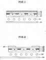
- FIG. 1is a cross section view illustrating the related art LCD device.
- the related art LCD deviceincludes an upper substrate 10, a lower substrate 20, and a liquid crystal layer 30 between the upper and lower substrates 10 and 20.
- a light-shielding layer 12On one surface of the upper substrate 10, and more particularly, one surface of the upper substrate 10 confronting the lower substrate 20, there is a light-shielding layer 12 to prevent light leakage. Also, red (R), green (G), and blue (B) color filter layers 14 are respectively formed between each light-shielding layer 12, to thereby display red (R), green (G), and blue (B) colors. For planarization of the upper substrate 10, an overcoat layer 16 is formed on the color filter layers 14.
- a thin film transistorOn one surface of the lower substrate 20, and more particularly, one surface of the lower substrate 20 confronting the upper substrate 10, there are a thin film transistor, a pixel electrode, and a common electrode, although not shown.
- the thin film transistorfunctions as a switching element, and the pixel electrode is electrically connected to the thin film transistor.
- the common electrodeis provided in parallel to the pixel electrode, whereby the common electrode, together with the pixel electrode, forms a parallel electric field.
- EP 10165404.4[0010] On the other surface of the upper substrate 10, and more particularly, the other surface of the upper substrate 10, which is not confronting the lower substrate 20, there is an ITO (Indium-Tin-Oxide) layer 40.
- ITOIndium-Tin-Oxide
- the ITO layer 40is provided to prevent a static electricity from occurring during a manufacturing process of the LCD device. That is, when the substrate is brought into contact with plural manufacturing and transferring apparatuses during the manufacturing process of the LCD device, the static electricity may occur. In order to prevent the static electricity from occurring during the manufacturing process of the LCD device, the ITO layer 40 as a conductive material layer is formed on the other surface of the upper substrate 10.
- the ITO layer 40 included in the related art LCD devicecan prevent the static electricity during the manufacturing process.
- user's touch sensitivitymight be lowered due to the ITO layer 40. That is, when a user touches a predetermined portion of the LCD device, the ITO layer 40 positioned on the upper side of the LCD device hinders the user's touch sensitivity, whereby it is difficult to exactly sense the touched portion.
- the capacitive type LCD device sensing the user's touch through the change of capacitancethe problem related with the deterioration of touch sensitivity get worse.
- US 2008/0151167 A1describes a liquid crystal display device including a first substrate and a second substrate.
- the second substrateis opposed to the first substrate and includes a translucent conductive film.
- the translucent conductive filmincludes a body portion and a pull-out portion.
- the body portionis opposed to a common electrode and pixel electrodes and may be provided without patterning (without any gaps), or, as long as it achieves a shielding effect against static electricity, it may be patterned to form a mesh.
- JP 9105918Adescribes a liquid crystal display device including two transparent substrates arranged to face each other, wherein a liquid crystal layer LC is interposed there between. On a surface of one transparent substrate a conductive layer having translucency is formed.
- US 6,597,414 B1describes a horizontal electric-field type LCD device.
- the deviceincludes a first substrate and a second substrate with liquid crystal confined in a space defined between the first and second substrates.
- a transparent conductive layeris formed, which is used for protecting the LCD device from an unwanted electric field.
- WO 2007/146785 A2describes liquid-crystal display (LCD) touch screens: A conductive black matrix layer provided below a top glass of the device may be used as a touch sense layer.
- LCDliquid-crystal display
- EP 0 917 174 A2describes an electromagnetic shielding bonding film carrying geometrically patterned electroconductive material.
- a line width of the geometric pattern and a line spacingis selected such that an aperture ratio is 50% or more.
- the present inventionis directed to an LCD device that substantially obviates one or more problems due to limitations and disadvantages of the related art.
- An advantage of the present inventionis to provide an LCD device which facilitates to prevent a static electricity during a manufacturing process, and to present deterioration in user's touch sensitivity.
- an LCD devicepreferably comprising: first and second substrate confronting each other; a liquid crystal layer between the first and second substrates; and a transparent electrode pattern layer in a predetermined pattern on one surface of the first substrate, which is not confronting the second substrate, for prevention of static electricity and improvement of touch sensitivity.
- the transparent electrode pattern layerincludes plural first patterns arranged at fixed intervals in a first direction.
- the first patternsare respectively connected to second patterns arranged in a second direction being different from the first direction.
- the first patternsinclude a region with a first width, and another region with a second width, wherein the first width is different from the second width.
- a pattern width of the transparent electrode pattern layeris 5 ⁇ 100 ⁇ m.
- the transparent electrode pattern layeris grounded while being connected to a ground pad on the second substrate.
- the transparent electrode pattern layeris connected to the ground pad through a conductive tape.
- the LCD devicefurther comprises a sensing electrode for sensing a user's touch on any one of the first and second substrates.
- the sensing electrodemay be formed of a common electrode on the second substrate, or a light-shielding layer on the first substrate.
- FIG. 2is a cross section view illustrating an LCD device according to one embodiment of the present invention.
- the LCD deviceincludes first and second substrates 100 and 200 confronting each other, and a liquid crystal layer 300 between the first and second substrates 100 and 200.
- a transparent electrode pattern layer 400On one surface of the first substrate 100, and more particularly, one surface of the first substrate 100 which is not confronting the second substrate 200, there is a transparent electrode pattern layer 400.
- a purpose of the transparent electrode pattern layer 400is to prevent a static electricity which occurs during a manufacturing process. Also, since the transparent electrode pattern layer 400 is formed in a predetermined pattern, instead of being formed on an entire area of one surface of the first substrate 100, it results in improvement in user's touch sensitivity. That is, as shown in the drawings, when the transparent electrode pattern layer 400 is formed in the predetermined pattern on one surface of the first substrate 100, a resistance of electrode is increased as compared to a related art LCD device with an ITO layer on an entire surface of the first substrate 100, to thereby result in improved touch sensitivity of sensing electrode. Especially, if a capacitive type LCD device senses a user's touch through a change of capacitance, the increased resistance of electrode enables the remarkably-improved touch sensitivity of sensing electrode.
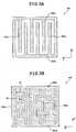
- a shape of the transparent electrode pattern layer 400may vary as shown in FIGs. 3A and 3B , but it is not limited to these shapes.
- the transparent electrode pattern layer 400may comprise plural first patterns 400a arranged in a first direction (y-direcfion), and plural second patterns 400b arranged in a second direction (x-direction) which is different from the first direction.
- the first patterns 400aare arranged at fixed intervals, and are respectively connected to the second patterns 400b. That is, the first patterns 400a are connected to the second patterns 400b, as a whole.
- the first patterns 400aare provided with a region with a first width (W1), and a region with a second width (W2), wherein the first width (W1) is different from the second width (W2).
- the first patterns 400a and second patterns 400b included in the transparent electrode pattern layer 400are properly adjusted in width so as to prevent static electricity during the manufacturing process, and to improve touch sensitivity.
- a low resistance of electrodeis profitable to prevent the static electricity occurring during the manufacturing process, and a high resistance of electrode is profitable to improve the touch sensitivity.
- the resistance of electrodeis adjusted in consideration for both static electricity and touch sensitivity, preferably.
- the resistance of electrodeis in inverse proportion to a width of electrode. In this respect, the width of electrode has to be properly adjusted based on the desirable resistance of electrode.
- a pattern width of the transparent electrode pattern layer 400In consideration for both static electricity and touch sensitivity, it is preferable that a pattern width of the transparent electrode pattern layer 400, and more particularly, a pattern width in each of the first patterns 400a and second patterns 400b have 5 ⁇ 100 ⁇ m. If the pattern width of the transparent electrode pattern layer 400 is less than 5 ⁇ m, the large resistance of electrode is such as to reduce the efficiency of preventing the static electricity. If the pattern width of the transparent electrode pattern layer 400 is more than 100 ⁇ m, the small resistance of electrode is such as to deteriorate the touch sensitivity.
- An interval between the patterns included in the transparent electrode pattern layer 400for example, an interval between the first patterns 400a, can be adjusted properly. In consideration for visibility, it is not preferable to provide the excessively large interval between the patterns. In detail, light transmitting through an area corresponding to the patterns included in the transparent electrode pattern layer 400 is different in transmittance from light transmitting through an area between the patterns included in the transparent electrode pattern layer 400. Thus, if the interval between the patterns included in the transparent electrode pattern layer 400 is too large, a difference of transmittance is too large to enhance the visibility. In this respect, it is preferable to provide the interval at a predetermined range allowing a user's unawareness.
- the transparent electrode pattern layer 400may be patterned by depositing a transparent conductive material such as ITO through the use of shadow mask.
- the transparent electrode pattern layer 400 on one surface of the first substrate 100may be grounded through the second substrate 200, which will be explained with reference to FIGs. 4A and 4B .
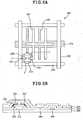
- FIG. 4Ais a plan view illustrating that the transparent electrode pattern layer 400 of the present invention is grounded through the second substrate 200; and FIG. 4B is a cross section view illustrating that the transparent electrode pattern layer 400 of the present invention is grounded through the second substrate 200.
- the transparent electrode pattern layer 400is formed on one surface of the first substrate 100, and a ground pad 201 is formed on one surface of the second substrate 200.
- the transparent electrode pattern layer 400is connected to the ground pad 201 through a conductor 500 such as a conductive tape. Since the transparent electrode pattern layer 400 is grounded through the second substrate 200, it is possible to prevent the static electricity from occurring during the manufacturing process.
- a light-shielding layer 120is formed on the other surface of the first substrate 100, wherein the other surface of the first substrate 100 indicates a surface which is confronting the second substrate 200.
- the light-shielding layer 120prevents the light from leaking in other regions except pixel regions, wherein the light-shielding layer 120 is patterned in a matrix configuration. Also, the light-shielding layer 120 may function as the sensing electrode. In this case, the light-shielding layer 120 includes a conductive material, and a signal-applying unit for applying a touch signal is connected to the light-shielding layer 120.
- each light-shielding layer 120there are red (R), green (G), and blue (B) color filter layers 140, respectively.
- the color filter layers 140may include additional yellow (Y), white (W), or cyan (CYAN) color filter layers as well as the red (R), green (G), and blue (B) color filter layers.
- an overcoat layer 160is formed on the color filter layers 140.
- the gate and data linescross each other at a right angle, to thereby the pixel region on the second substrate 200.
- the thin film transistorwhich functions as a switching element, is formed at a crossing portion of the gate and data lines.
- the common electrodeis provided in parallel to a pixel electrode.
- a structure of the second substrate 200will be explained as follows.
- the following structure of the second substrate 200is only one example, that is, it is not limited to this structure.
- FIG. 5Ais a plan view illustrating the second substrate according to one embodiment of the present invention.
- FIG. 5Bis a cross section view along I-I of FIG. 5A.
- FIGs. 5A and 5Billustrate only one pixel of the LCD device.
- the gate and data lines 210 and 230 crossing each other at a right angleare formed on the second substrate 200.
- the thin film transistor (T)At the crossing portion of the gate and data lines 210 and 230, there is the thin film transistor (T).
- the thin film transistor (T)includes a gate electrode 212, a semiconductor layer 220, a source electrode 232, and a drain electrode 234.
- the gate electrode 212is prominently diverged from the gate line 210; the source electrode 232 is prominently diverged from the data line 230; and the drain electrode 234 is provided at a predetermined interval from the source electrode 232.
- the pixel electrode 240is connected to the thin film transistor (T).
- the pixel electrode 240is connected to the drain electrode 234 of the thin film transistor (T).
- the common electrode 250is provided in parallel to the pixel electrode 240, whereby the common electrode 250 together with the pixel electrode 240 forms a parallel electric field.
- the common electrode 250is diverged from a common line 252, wherein the common electrode 250 functions as the sensing electrode.
- the signal-applying. unit for applying the touch signalis connected to the common electrode 250.
- the gate electrode 212is formed on the second substrate 200; and a gate insulation film 215 is formed on the second substrate 200 including the gate electrode 212.
- the semiconductor layer 220On the gate insulation film 215, there is the semiconductor layer 220.
- source and drain electrodes 232 and 234are formed on the semiconductor layer 220, wherein the source and drain electrodes 232 and 234 are provided at a predetermined interval therebetween.
- the semiconductor layer 220comprises an ohmic contact layer 222 doped with impurities, which is in contact with the source electrode 232 and the drain electrode 234.
- a passivation film 245is formed on the source and drain electrodes 232 and 234.
- the pixel electrode 240 and the common electrode 250are formed in the pixel region.
- the pixel electrode 240is formed on the gate insulation film 215. That is, the pixel electrode 240 is formed at the same layer as the source and drain electrodes 232 and 234. Especially, the pixel electrode 240 extends from the drain electrode 234.
- the common electrode 250is formed on the second substrate 200, and is positioned under the gate insulation film 215. That is, the common electrode 250 is formed at the same layer as the gate electrode 212.
- FIG. 6Ais a plan view illustrating the second substrate according to another embodiment of the present invention
- FIG. 6Bis a cross section view along I-I of FIG. 6A
- the second substrate shown in FIGs. 6A and 6Bis identical in structure to the second substrate shown in FIGs. 5A and 5B , whereby the same reference numbers will be used throughout the drawings to refer to the same or like parts, and a detailed explanation for the same parts will be omitted.
- the common electrode 250 and the common line 252are formed on the passivation film 245.
- the parallel electric fieldis applied through the pixel electrode 240 and common electrode 250 formed at the different layers, but it is not limited to this structure.
- the parallel electric fieldmay be applied through the pixel electrode 240 and common electrode 250 formed at the same layer. That is, both the pixel electrode 240 and common electrode 250 may be formed on the passivation film 245, or may be formed on the gate insulation film 215.
- alignment layersare respectively formed on the first and second substrates 100 and 200.
- the alignment layersare provided to an initial alignment of liquid crystal molecules in the liquid crystal layer 300.
- the alignment layerscorrespond to the uppermost layers of the respective first and second substrates 100 and 200.
- first and second substrates 100 and 200are bonded to each other by a sealant provided in the circumference of the substrates, and spacers for maintenance of a cell gap are additionally provided between the first and second substrates 100 and 200.
- the transparent electrode pattern layer 400is formed in the predetermined pattern on one surface of the first substrate 100, which enables to prevent the static electricity during the manufacturing process, and to improve the user's touch sensitivity through the increased resistance of electrode.
- the touch sensitivity of sensing electrodecan be highly improved.
Landscapes
- Physics & Mathematics (AREA)
- Nonlinear Science (AREA)
- Engineering & Computer Science (AREA)
- General Physics & Mathematics (AREA)
- Crystallography & Structural Chemistry (AREA)
- Chemical & Material Sciences (AREA)
- Mathematical Physics (AREA)
- Optics & Photonics (AREA)
- General Engineering & Computer Science (AREA)
- Theoretical Computer Science (AREA)
- Human Computer Interaction (AREA)
- Geometry (AREA)
- Electromagnetism (AREA)
- Liquid Crystal (AREA)
- Position Input By Displaying (AREA)
Description
- This application claims the benefit of the Korean Patent Application No.
10-2009-0111480 filed on November 18, 2009 - The present invention relates to a liquid crystal display (LCD) device, and more particularly, to an LCD device capable of sensing a user's touch signal.
- An LCD device can realize low power consumption owing to a low driving voltage, and also the LCD device is suitable for a portable. In this respect, the LCD device is widely used in various fields of notebook computer, monitor, spacecraft, aircraft, and etc.
- The LCD device includes a lower substrate, an upper substrate, and a liquid crystal layer between the lower and upper substrates. In case of the LCD device, an alignment state of liquid crystal molecules in the liquid crystal layer is controlled based on whether or not an electric field is applied thereto, and light transmittance is controlled according to the alignment state of liquid crystal molecules, whereby images are displayed thereon.
- Furthermore, the LCD device capable of sensing a user's touch signal has been developed for the notebook computer, in which a position-sensing device having a sensing electrode is provided to sense the user's touch signal.
- The LCD device with the position-sensing device may be largely classified into a resistive type, a capacitive type, and an electro-magnetic type according to a position-sensing method. The resistive type LCD device senses a change of current which occurs due to a pressure based on a user's touch; the capacitive type LCD device senses a change of capacitance which occurs by a user's touch; and the electro-magnetic type LCD device senses a portion selected by a user through a change of voltage under the circumstance an electric field is applied thereto.
- Hereinafter, a related art LCD device will be described with reference to the accompanying drawings.
FIG. 1 is a cross section view illustrating the related art LCD device.- As shown in
FIG. 1 , the related art LCD device includes anupper substrate 10, alower substrate 20, and a liquid crystal layer 30 between the upper andlower substrates - On one surface of the
upper substrate 10, and more particularly, one surface of theupper substrate 10 confronting thelower substrate 20, there is a light-shielding layer 12 to prevent light leakage. Also, red (R), green (G), and blue (B)color filter layers 14 are respectively formed between each light-shielding layer 12, to thereby display red (R), green (G), and blue (B) colors. For planarization of theupper substrate 10, anovercoat layer 16 is formed on thecolor filter layers 14. - On one surface of the
lower substrate 20, and more particularly, one surface of thelower substrate 20 confronting theupper substrate 10, there are a thin film transistor, a pixel electrode, and a common electrode, although not shown. The thin film transistor functions as a switching element, and the pixel electrode is electrically connected to the thin film transistor. The common electrode is provided in parallel to the pixel electrode, whereby the common electrode, together with the pixel electrode, forms a parallel electric field. EP 10165404.4 upper substrate 10, and more particularly, the other surface of theupper substrate 10, which is not confronting thelower substrate 20, there is an ITO (Indium-Tin-Oxide)layer 40.- The ITO
layer 40 is provided to prevent a static electricity from occurring during a manufacturing process of the LCD device. That is, when the substrate is brought into contact with plural manufacturing and transferring apparatuses during the manufacturing process of the LCD device, the static electricity may occur. In order to prevent the static electricity from occurring during the manufacturing process of the LCD device, theITO layer 40 as a conductive material layer is formed on the other surface of theupper substrate 10. - The ITO
layer 40 included in the related art LCD device can prevent the static electricity during the manufacturing process. However, in case of the LCD device with the position-sensing device, user's touch sensitivity might be lowered due to theITO layer 40. That is, when a user touches a predetermined portion of the LCD device, theITO layer 40 positioned on the upper side of the LCD device hinders the user's touch sensitivity, whereby it is difficult to exactly sense the touched portion. Especially, in case of the capacitive type LCD device sensing the user's touch through the change of capacitance, the problem related with the deterioration of touch sensitivity get worse. US 2008/0151167 A1 describes a liquid crystal display device including a first substrate and a second substrate. The second substrate is opposed to the first substrate and includes a translucent conductive film. The translucent conductive film includes a body portion and a pull-out portion. The body portion is opposed to a common electrode and pixel electrodes and may be provided without patterning (without any gaps), or, as long as it achieves a shielding effect against static electricity, it may be patterned to form a mesh.JP 9105918A US 6,597,414 B1 describes a horizontal electric-field type LCD device. The device includes a first substrate and a second substrate with liquid crystal confined in a space defined between the first and second substrates. On an outer surface of the first substrate a transparent conductive layer is formed, which is used for protecting the LCD device from an unwanted electric field.WO 2007/146785 A2 describes liquid-crystal display (LCD) touch screens: A conductive black matrix layer provided below a top glass of the device may be used as a touch sense layer.EP 0 917 174 A2 describes an electromagnetic shielding bonding film carrying geometrically patterned electroconductive material. A line width of the geometric pattern and a line spacing is selected such that an aperture ratio is 50% or more.- Accordingly, the present invention is directed to an LCD device that substantially obviates one or more problems due to limitations and disadvantages of the related art.
- An advantage of the present invention is to provide an LCD device which facilitates to prevent a static electricity during a manufacturing process, and to present deterioration in user's touch sensitivity.
- Additional advantages and features of the invention will be set forth in part in the description which follows and in part will become apparent to those having ordinary skill in the art upon examination of the following or may be learned from practice of the invention. The objectives and other advantages of the invention may be realized and attained by the structure particularly pointed out in the written description and claims hereof as well as the appended drawings.
- The object is solved by the features of the independent claim.
- To achieve these and other advantages and in accordance with the purpose of the invention, as embodied and broadly described herein, there is provided an LCD device preferably comprising: first and second substrate confronting each other; a liquid crystal layer between the first and second substrates; and a transparent electrode pattern layer in a predetermined pattern on one surface of the first substrate, which is not confronting the second substrate, for prevention of static electricity and improvement of touch sensitivity.
- At this time, the transparent electrode pattern layer includes plural first patterns arranged at fixed intervals in a first direction. In this case, the first patterns are respectively connected to second patterns arranged in a second direction being different from the first direction. Also, the first patterns include a region with a first width, and another region with a second width, wherein the first width is different from the second width.
- At this time, a pattern width of the transparent electrode pattern layer is 5 ∼ 100µm.
- The transparent electrode pattern layer is grounded while being connected to a ground pad on the second substrate. In this case, the transparent electrode pattern layer is connected to the ground pad through a conductive tape.
- In addition, the LCD device further comprises a sensing electrode for sensing a user's touch on any one of the first and second substrates. In this case, the sensing electrode may be formed of a common electrode on the second substrate, or a light-shielding layer on the first substrate.
- It is to be understood that both the foregoing general description and the following detailed description of the present invention are exemplary and explanatory and are intended to provide further explanation of the invention as claimed.
- The accompanying drawings, which are included to provide a further understanding of the invention and are incorporated in and constitute a part of this application, illustrate embodiment(s) of the invention and together with the description serve to explain the principle of the invention. In the drawings:
FIG. 1 is a cross section view illustrating an LCD device according to the related art;FIG. 2 is a cross section view illustrating an LCD device according to one embodiment of the present invention;FIGs. 3A and 3B are plan views illustrating transparent electrode pattern layers according to various embodiments of the present invention;FIG. 4A is a plan view illustrating that a transparent electrode pattern layer is grounded through a second substrate in the LCD device according to the present invention, andFIG. 4B is a cross section view illustrating that a transparent electrode pattern layer is grounded through a second substrate in the LCD device according to the present invention;FIG. 5A is a plan view illustrating a second substrate according to one embodiment of the present invention, andFIG. 5B is a cross section view along I-I ofFIG. 5A ; andFIG. 6A is a plan view illustrating a second substrate according to another embodiment of the present invention, andFIG. 6B is a cross section view along I-I ofFIG. 6A .- Reference will now be made in detail to the exemplary embodiments of the present invention, examples of which are illustrated in the accompanying drawings. Wherever possible, the same reference numbers will be used throughout the drawings to refer to the same or like parts.
- Hereinafter, an LCD device according to the present invention will be described with reference to the accompanying drawings.
FIG. 2 is a cross section view illustrating an LCD device according to one embodiment of the present invention.- As shown in
FIG. 2 , the LCD device according to one embodiment of the present invention includes first andsecond substrates liquid crystal layer 300 between the first andsecond substrates - On one surface of the
first substrate 100, and more particularly, one surface of thefirst substrate 100 which is not confronting thesecond substrate 200, there is a transparentelectrode pattern layer 400. - A purpose of the transparent
electrode pattern layer 400 is to prevent a static electricity which occurs during a manufacturing process. Also, since the transparentelectrode pattern layer 400 is formed in a predetermined pattern, instead of being formed on an entire area of one surface of thefirst substrate 100, it results in improvement in user's touch sensitivity. That is, as shown in the drawings, when the transparentelectrode pattern layer 400 is formed in the predetermined pattern on one surface of thefirst substrate 100, a resistance of electrode is increased as compared to a related art LCD device with an ITO layer on an entire surface of thefirst substrate 100, to thereby result in improved touch sensitivity of sensing electrode. Especially, if a capacitive type LCD device senses a user's touch through a change of capacitance, the increased resistance of electrode enables the remarkably-improved touch sensitivity of sensing electrode. - A shape of the transparent
electrode pattern layer 400 may vary as shown inFIGs. 3A and 3B , but it is not limited to these shapes. - As shown in
FIGs. 3A and 3B , the transparentelectrode pattern layer 400 may comprise pluralfirst patterns 400a arranged in a first direction (y-direcfion), and pluralsecond patterns 400b arranged in a second direction (x-direction) which is different from the first direction. - The
first patterns 400a are arranged at fixed intervals, and are respectively connected to thesecond patterns 400b. That is, thefirst patterns 400a are connected to thesecond patterns 400b, as a whole. - As shown in
FIG. 3B , thefirst patterns 400a are provided with a region with a first width (W1), and a region with a second width (W2), wherein the first width (W1) is different from the second width (W2). - The
first patterns 400a andsecond patterns 400b included in the transparentelectrode pattern layer 400 are properly adjusted in width so as to prevent static electricity during the manufacturing process, and to improve touch sensitivity. - In more detail, a low resistance of electrode is profitable to prevent the static electricity occurring during the manufacturing process, and a high resistance of electrode is profitable to improve the touch sensitivity. Thus, the resistance of electrode is adjusted in consideration for both static electricity and touch sensitivity, preferably. The resistance of electrode is in inverse proportion to a width of electrode. In this respect, the width of electrode has to be properly adjusted based on the desirable resistance of electrode.
- In consideration for both static electricity and touch sensitivity, it is preferable that a pattern width of the transparent
electrode pattern layer 400, and more particularly, a pattern width in each of thefirst patterns 400a andsecond patterns 400b have 5 ∼ 100µm. If the pattern width of the transparentelectrode pattern layer 400 is less than 5µm, the large resistance of electrode is such as to reduce the efficiency of preventing the static electricity. If the pattern width of the transparentelectrode pattern layer 400 is more than 100µm, the small resistance of electrode is such as to deteriorate the touch sensitivity. - An interval between the patterns included in the transparent
electrode pattern layer 400, for example, an interval between thefirst patterns 400a, can be adjusted properly. In consideration for visibility, it is not preferable to provide the excessively large interval between the patterns. In detail, light transmitting through an area corresponding to the patterns included in the transparentelectrode pattern layer 400 is different in transmittance from light transmitting through an area between the patterns included in the transparentelectrode pattern layer 400. Thus, if the interval between the patterns included in the transparentelectrode pattern layer 400 is too large, a difference of transmittance is too large to enhance the visibility. In this respect, it is preferable to provide the interval at a predetermined range allowing a user's unawareness. - The transparent
electrode pattern layer 400 may be patterned by depositing a transparent conductive material such as ITO through the use of shadow mask. - The transparent
electrode pattern layer 400 on one surface of thefirst substrate 100 may be grounded through thesecond substrate 200, which will be explained with reference toFIGs. 4A and 4B . FIG. 4A is a plan view illustrating that the transparentelectrode pattern layer 400 of the present invention is grounded through thesecond substrate 200; andFIG. 4B is a cross section view illustrating that the transparentelectrode pattern layer 400 of the present invention is grounded through thesecond substrate 200.- As shown in
FIGs. 4A and 4B , the transparentelectrode pattern layer 400 is formed on one surface of thefirst substrate 100, and aground pad 201 is formed on one surface of thesecond substrate 200. - Also, the transparent
electrode pattern layer 400 is connected to theground pad 201 through aconductor 500 such as a conductive tape. Since the transparentelectrode pattern layer 400 is grounded through thesecond substrate 200, it is possible to prevent the static electricity from occurring during the manufacturing process. - Referring once again to
FIG. 2 , a light-shielding layer 120 is formed on the other surface of thefirst substrate 100, wherein the other surface of thefirst substrate 100 indicates a surface which is confronting thesecond substrate 200. - The light-
shielding layer 120 prevents the light from leaking in other regions except pixel regions, wherein the light-shielding layer 120 is patterned in a matrix configuration. Also, the light-shielding layer 120 may function as the sensing electrode. In this case, the light-shielding layer 120 includes a conductive material, and a signal-applying unit for applying a touch signal is connected to the light-shielding layer 120. - Between each light-
shielding layer 120, there are red (R), green (G), and blue (B) color filter layers 140, respectively. As shown in the drawings, the color filter layers 140 may include additional yellow (Y), white (W), or cyan (CYAN) color filter layers as well as the red (R), green (G), and blue (B) color filter layers. - For planarization of the substrate, an
overcoat layer 160 is formed on the color filter layers 140. - On the
second substrate 200, there are gate and data lines, a thin film transistor, and a common electrode. The gate and data lines cross each other at a right angle, to thereby the pixel region on thesecond substrate 200. The thin film transistor, which functions as a switching element, is formed at a crossing portion of the gate and data lines. In the pixel region, the common electrode is provided in parallel to a pixel electrode. - A structure of the
second substrate 200 will be explained as follows. The following structure of thesecond substrate 200 is only one example, that is, it is not limited to this structure. FIG. 5A is a plan view illustrating the second substrate according to one embodiment of the present invention; andFIG. 5B is a cross section view along I-I ofFIG. 5A. FIGs. 5A and 5B illustrate only one pixel of the LCD device.- As shown in
FIG. 5A , the gate anddata lines second substrate 200. At the crossing portion of the gate anddata lines - The thin film transistor (T) includes a
gate electrode 212, asemiconductor layer 220, asource electrode 232, and adrain electrode 234. - The
gate electrode 212 is prominently diverged from thegate line 210; thesource electrode 232 is prominently diverged from thedata line 230; and thedrain electrode 234 is provided at a predetermined interval from thesource electrode 232. - The
pixel electrode 240 is connected to the thin film transistor (T). In detail, thepixel electrode 240 is connected to thedrain electrode 234 of the thin film transistor (T). - The
common electrode 250 is provided in parallel to thepixel electrode 240, whereby thecommon electrode 250 together with thepixel electrode 240 forms a parallel electric field. Thecommon electrode 250 is diverged from acommon line 252, wherein thecommon electrode 250 functions as the sensing electrode. In this case, the signal-applying. unit for applying the touch signal is connected to thecommon electrode 250. - As shown in
FIG. 5B , thegate electrode 212 is formed on thesecond substrate 200; and agate insulation film 215 is formed on thesecond substrate 200 including thegate electrode 212. On thegate insulation film 215, there is thesemiconductor layer 220. Then, source and drainelectrodes semiconductor layer 220, wherein the source and drainelectrodes semiconductor layer 220 comprises anohmic contact layer 222 doped with impurities, which is in contact with thesource electrode 232 and thedrain electrode 234. Then, apassivation film 245 is formed on the source and drainelectrodes - In the meantime, the
pixel electrode 240 and thecommon electrode 250 are formed in the pixel region. - The
pixel electrode 240 is formed on thegate insulation film 215. That is, thepixel electrode 240 is formed at the same layer as the source and drainelectrodes pixel electrode 240 extends from thedrain electrode 234. - The
common electrode 250 is formed on thesecond substrate 200, and is positioned under thegate insulation film 215. That is, thecommon electrode 250 is formed at the same layer as thegate electrode 212. FIG. 6A is a plan view illustrating the second substrate according to another embodiment of the present invention; andFIG. 6B is a cross section view along I-I ofFIG. 6A . Except positions of thecommon electrode 250 and thecommon line 252, the second substrate shown inFIGs. 6A and 6B is identical in structure to the second substrate shown inFIGs. 5A and 5B , whereby the same reference numbers will be used throughout the drawings to refer to the same or like parts, and a detailed explanation for the same parts will be omitted.- Referring to
FIGs. 6A and 6B , thecommon electrode 250 and thecommon line 252 are formed on thepassivation film 245. - In the
second substrate 200 according to the embodiments of the present invention, the parallel electric field is applied through thepixel electrode 240 andcommon electrode 250 formed at the different layers, but it is not limited to this structure. For example, the parallel electric field may be applied through thepixel electrode 240 andcommon electrode 250 formed at the same layer. That is, both thepixel electrode 240 andcommon electrode 250 may be formed on thepassivation film 245, or may be formed on thegate insulation film 215. - Although not shown, alignment layers are respectively formed on the first and
second substrates liquid crystal layer 300. The alignment layers correspond to the uppermost layers of the respective first andsecond substrates - Also, the first and
second substrates second substrates - As mentioned above, the transparent
electrode pattern layer 400 is formed in the predetermined pattern on one surface of thefirst substrate 100, which enables to prevent the static electricity during the manufacturing process, and to improve the user's touch sensitivity through the increased resistance of electrode. - Especially, in case of the capacitive type LCD device which senses the user's touch signal through the change of capacitance, the touch sensitivity of sensing electrode can be highly improved.
- It will be apparent to those skilled in the art that various modifications and variations can be made in the present invention. Thus, it is intended that the present invention covers the modifications and variations of this invention provided they come within the scope of the appended claims and their equivalents.
Claims (8)
- An LCD device comprising:first and second substrate (100, 200) confronting each other;a liquid crystal layer (300) between the first and second substrates (100, 200); anda transparent electrode pattern layer (400) in a predetermined pattern on one surface of the first substrate (100, 200), which is not confronting the second substrate (200), for prevention of static electricity and improvement of touch sensitivity,whereas transparent electrode pattern layer (400) includes plural first patterns (400a) arranged at fixed intervals in a first direction,characterized in that the first patterns (400a) include a region with a first width (W1) in the first direction and another region with a second width (W2) in the first direction, wherein the first width (W1) is different from the second width (W2).
- The LCD device according to claim 1, wherein the first patterns (400a) are respectively connected to second patterns (400b) arranged in a second direction being different from the first direction.
- The LCD device according to claim 1, wherein a pattern width of the first patterns (400a) in the first direction a pattern width of the second patterns (400b) in the second direction is 5 ∼ 100µm, respectively
- The LCD device according to claim 1, wherein the transparent electrode pattern layer (400) is grounded while being connected to a ground pad (201) on the second substrate (200).
- The LCD device according to claim 4, wherein the transparent electrode pattern layer (400) is connected to the ground pad (201) through a conductive tape (500).
- The LCD device according to claim 1, further comprising a sensing electrode (250) for sensing a user's touch on any one of the first and second substrates (100, 200).
- The LCD device according to claim 6, wherein pixel and common electrodes (240, 250) are formed in parallel on the second substrate (200), and the sensing electrode (250) is formed of the common electrode on the second substrate (200).
- The LCD device according to claim 6, wherein a light-shielding layer (120) and color filter layers (140) are formed on the first substrate (100), and the sensing electrode (250) is formed of the light-shielding layer (120) on the first substrate (100).
Applications Claiming Priority (1)
| Application Number | Priority Date | Filing Date | Title |
|---|---|---|---|
| KR1020090111480AKR20110054725A (en) | 2009-11-18 | 2009-11-18 | LCD Display |
Publications (3)
| Publication Number | Publication Date |
|---|---|
| EP2325690A2 EP2325690A2 (en) | 2011-05-25 |
| EP2325690A3 EP2325690A3 (en) | 2011-12-14 |
| EP2325690B1true EP2325690B1 (en) | 2016-07-20 |
Family
ID=43499956
Family Applications (1)
| Application Number | Title | Priority Date | Filing Date |
|---|---|---|---|
| EP10165404.4AActiveEP2325690B1 (en) | 2009-11-18 | 2010-06-09 | Liquid crystal display device |
Country Status (5)
| Country | Link |
|---|---|
| US (1) | US20110115739A1 (en) |
| EP (1) | EP2325690B1 (en) |
| KR (1) | KR20110054725A (en) |
| CN (1) | CN102062964A (en) |
| PL (1) | PL2325690T3 (en) |
Families Citing this family (17)
| Publication number | Priority date | Publication date | Assignee | Title |
|---|---|---|---|---|
| KR101958008B1 (en)* | 2011-06-17 | 2019-03-15 | 엘지디스플레이 주식회사 | Organic Light Emitting Display Device |
| JP2015121829A (en)* | 2012-04-18 | 2015-07-02 | シャープ株式会社 | Color filter integrated touch panel |
| US9001280B2 (en) | 2012-06-08 | 2015-04-07 | Apple Inc. | Devices and methods for shielding displays from electrostatic discharge |
| KR102051465B1 (en)* | 2012-06-18 | 2019-12-05 | 삼성디스플레이 주식회사 | Organic light emitting display device |
| KR20140024149A (en)* | 2012-08-20 | 2014-02-28 | 삼성전기주식회사 | Touch panel and method for manufacturing the same |
| CN102955303B (en)* | 2012-10-26 | 2016-04-06 | 北京京东方光电科技有限公司 | A kind of touching display screen and touch control display apparatus |
| FR2998682B1 (en)* | 2012-11-26 | 2016-01-15 | Volfoni R&D | OPTICAL POLARIZATION MODULATOR WITH LIQUID CRYSTALS |
| TWI584028B (en)* | 2012-12-28 | 2017-05-21 | 鴻海精密工業股份有限公司 | Liquid crystal display panel and thin film transistor substrate |
| EP2887185B1 (en)* | 2013-12-20 | 2016-11-09 | LG Display Co., Ltd. | Display device integrated with touch screen panel and method of driving the same |
| KR102127882B1 (en)* | 2013-12-26 | 2020-06-29 | 엘지디스플레이 주식회사 | Flexible display device and method of manufacturing the same |
| JP2016206322A (en)* | 2015-04-20 | 2016-12-08 | 三菱電機株式会社 | Liquid crystal display |
| CN105425443A (en)* | 2015-12-04 | 2016-03-23 | 江西沃格光电股份有限公司 | Embedded touch screen with high-resistance film and display device |
| CN105425455A (en)* | 2015-12-31 | 2016-03-23 | 武汉华星光电技术有限公司 | Embedded touch display panel and preparation technology thereof |
| US10788943B2 (en)* | 2016-12-15 | 2020-09-29 | Sharp Kabushiki Kaisha | Touch panel-equipped display device |
| CN107229164B (en)* | 2017-07-20 | 2020-10-09 | 武汉华星光电技术有限公司 | Color film substrate and liquid crystal panel manufacturing equipment |
| KR102555984B1 (en)* | 2018-07-27 | 2023-07-14 | 삼성디스플레이 주식회사 | Display device with a force sensor |
| KR102702297B1 (en) | 2018-10-17 | 2024-09-03 | 삼성디스플레이 주식회사 | Display device |
Family Cites Families (13)
| Publication number | Priority date | Publication date | Assignee | Title |
|---|---|---|---|---|
| JP2758864B2 (en)* | 1995-10-12 | 1998-05-28 | 株式会社日立製作所 | Liquid crystal display |
| US6086979A (en)* | 1997-11-11 | 2000-07-11 | Hitachi Chemical Company, Ltd. | Electromagnetically shielding bonding film, and shielding assembly and display device using such film |
| JP3107078B2 (en)* | 1999-02-26 | 2000-11-06 | 日本電気株式会社 | Liquid crystal display |
| CN1288951C (en)* | 2001-03-02 | 2006-12-06 | 日立化成工业株式会社 | Electromagnetic wave shielding film, electromagnetic wave shielding component and display |
| TW526706B (en)* | 2002-06-28 | 2003-04-01 | Ponwei Hou | Materials for electromagnetic wave shielding film |
| CN102981678B (en)* | 2006-06-09 | 2015-07-22 | 苹果公司 | Touch screen liquid crystal display |
| US8259078B2 (en)* | 2006-06-09 | 2012-09-04 | Apple Inc. | Touch screen liquid crystal display |
| CN101131618A (en)* | 2006-08-20 | 2008-02-27 | 陈其良 | Pixel-multiplexing touch control type flat panel display |
| JP4501933B2 (en)* | 2006-12-26 | 2010-07-14 | エプソンイメージングデバイス株式会社 | Liquid crystal display |
| US7796224B2 (en)* | 2006-12-26 | 2010-09-14 | Sony Corporation | Liquid crystal display device |
| JP2008281616A (en)* | 2007-05-08 | 2008-11-20 | Seiko Epson Corp | Liquid crystal device and electronic device |
| TWM343210U (en)* | 2008-05-30 | 2008-10-21 | Tpk Touch Solutions Inc | Display panel integrating the touch-control structure |
| US8508495B2 (en)* | 2008-07-03 | 2013-08-13 | Apple Inc. | Display with dual-function capacitive elements |
- 2009
- 2009-11-18KRKR1020090111480Apatent/KR20110054725A/ennot_activeCeased
- 2010
- 2010-06-09EPEP10165404.4Apatent/EP2325690B1/enactiveActive
- 2010-06-09PLPL10165404Tpatent/PL2325690T3/enunknown
- 2010-06-22CNCN2010102121977Apatent/CN102062964A/enactivePending
- 2010-06-30USUS12/827,996patent/US20110115739A1/ennot_activeAbandoned
Also Published As
| Publication number | Publication date |
|---|---|
| US20110115739A1 (en) | 2011-05-19 |
| EP2325690A3 (en) | 2011-12-14 |
| PL2325690T3 (en) | 2017-01-31 |
| CN102062964A (en) | 2011-05-18 |
| EP2325690A2 (en) | 2011-05-25 |
| KR20110054725A (en) | 2011-05-25 |
Similar Documents
| Publication | Publication Date | Title |
|---|---|---|
| EP2325690B1 (en) | Liquid crystal display device | |
| KR101009672B1 (en) | Touch Panel Built-in Liquid Crystal Display | |
| US8792061B2 (en) | Liquid crystal display device | |
| US8289457B2 (en) | Liquid crystal display including touch sensor layer and manufacturing method thereof | |
| US10126585B2 (en) | Liquid crystal display device | |
| EP3296809B1 (en) | Liquid crystal display device | |
| KR101288397B1 (en) | IPS type liquid crystal display with touch function | |
| US9176339B2 (en) | Liquid crystal display device | |
| TWI461792B (en) | Liquid crystal display with built-in touch screen panel | |
| US9483984B2 (en) | Touch sensing display device | |
| TWI533185B (en) | Touch panel substrate and electro-optical apparatus | |
| US20110187669A1 (en) | Liquid crystal display device and manufacting method thereof | |
| US9557594B2 (en) | Liquid-crystal display screen with touch-control function and manufacturing method thereof and electronic apparatus | |
| KR20090049981A (en) | Transverse electric field liquid crystal display device | |
| US8730414B2 (en) | Liquid crystal display device including various embodiments of light-shielding line | |
| CN111679524A (en) | Display panel and display device | |
| CN104461182B (en) | Touch element and flat display device | |
| TWI755028B (en) | In-cell touch display panel | |
| KR101859469B1 (en) | Display device and manufacturing method thereof | |
| CN118605058B (en) | Display panel and display device | |
| CN116661190A (en) | Display panel and display device | |
| KR20130010539A (en) | Liquid crystal display device | |
| TW201502657A (en) | Touch IPS liquid crystal display |
Legal Events
| Date | Code | Title | Description |
|---|---|---|---|
| PUAI | Public reference made under article 153(3) epc to a published international application that has entered the european phase | Free format text:ORIGINAL CODE: 0009012 | |
| AK | Designated contracting states | Kind code of ref document:A2 Designated state(s):AL AT BE BG CH CY CZ DE DK EE ES FI FR GB GR HR HU IE IS IT LI LT LU LV MC MK MT NL NO PL PT RO SE SI SK SM TR | |
| AX | Request for extension of the european patent | Extension state:BA ME RS | |
| PUAL | Search report despatched | Free format text:ORIGINAL CODE: 0009013 | |
| AK | Designated contracting states | Kind code of ref document:A3 Designated state(s):AL AT BE BG CH CY CZ DE DK EE ES FI FR GB GR HR HU IE IS IT LI LT LU LV MC MK MT NL NO PL PT RO SE SI SK SM TR | |
| AX | Request for extension of the european patent | Extension state:BA ME RS | |
| RIC1 | Information provided on ipc code assigned before grant | Ipc:G02F 1/133 20060101AFI20111110BHEP | |
| 17P | Request for examination filed | Effective date:20120613 | |
| 17Q | First examination report despatched | Effective date:20130816 | |
| REG | Reference to a national code | Ref country code:DE Ref legal event code:R079 Ref document number:602010034792 Country of ref document:DE Free format text:PREVIOUS MAIN CLASS: G02F0001133000 Ipc:G02F0001133300 | |
| GRAP | Despatch of communication of intention to grant a patent | Free format text:ORIGINAL CODE: EPIDOSNIGR1 | |
| RIC1 | Information provided on ipc code assigned before grant | Ipc:G02F 1/1333 20060101AFI20151109BHEP Ipc:G02F 1/1343 20060101ALI20151109BHEP Ipc:G06F 3/041 20060101ALI20151109BHEP | |
| INTG | Intention to grant announced | Effective date:20151202 | |
| RAP1 | Party data changed (applicant data changed or rights of an application transferred) | Owner name:LG DISPLAY CO., LTD. | |
| GRAS | Grant fee paid | Free format text:ORIGINAL CODE: EPIDOSNIGR3 | |
| GRAJ | Information related to disapproval of communication of intention to grant by the applicant or resumption of examination proceedings by the epo deleted | Free format text:ORIGINAL CODE: EPIDOSDIGR1 | |
| GRAP | Despatch of communication of intention to grant a patent | Free format text:ORIGINAL CODE: EPIDOSNIGR1 | |
| GRAP | Despatch of communication of intention to grant a patent | Free format text:ORIGINAL CODE: EPIDOSNIGR1 | |
| GRAS | Grant fee paid | Free format text:ORIGINAL CODE: EPIDOSNIGR3 | |
| INTG | Intention to grant announced | Effective date:20160502 | |
| GRAA | (expected) grant | Free format text:ORIGINAL CODE: 0009210 | |
| AK | Designated contracting states | Kind code of ref document:B1 Designated state(s):AL AT BE BG CH CY CZ DE DK EE ES FI FR GB GR HR HU IE IS IT LI LT LU LV MC MK MT NL NO PL PT RO SE SI SK SM TR | |
| REG | Reference to a national code | Ref country code:GB Ref legal event code:FG4D | |
| REG | Reference to a national code | Ref country code:CH Ref legal event code:EP | |
| REG | Reference to a national code | Ref country code:IE Ref legal event code:FG4D | |
| REG | Reference to a national code | Ref country code:AT Ref legal event code:REF Ref document number:814538 Country of ref document:AT Kind code of ref document:T Effective date:20160815 | |
| REG | Reference to a national code | Ref country code:DE Ref legal event code:R096 Ref document number:602010034792 Country of ref document:DE | |
| REG | Reference to a national code | Ref country code:NL Ref legal event code:FP | |
| REG | Reference to a national code | Ref country code:LT Ref legal event code:MG4D | |
| REG | Reference to a national code | Ref country code:AT Ref legal event code:MK05 Ref document number:814538 Country of ref document:AT Kind code of ref document:T Effective date:20160720 | |
| PG25 | Lapsed in a contracting state [announced via postgrant information from national office to epo] | Ref country code:LT Free format text:LAPSE BECAUSE OF FAILURE TO SUBMIT A TRANSLATION OF THE DESCRIPTION OR TO PAY THE FEE WITHIN THE PRESCRIBED TIME-LIMIT Effective date:20160720 Ref country code:FI Free format text:LAPSE BECAUSE OF FAILURE TO SUBMIT A TRANSLATION OF THE DESCRIPTION OR TO PAY THE FEE WITHIN THE PRESCRIBED TIME-LIMIT Effective date:20160720 Ref country code:IS Free format text:LAPSE BECAUSE OF FAILURE TO SUBMIT A TRANSLATION OF THE DESCRIPTION OR TO PAY THE FEE WITHIN THE PRESCRIBED TIME-LIMIT Effective date:20161120 Ref country code:NO Free format text:LAPSE BECAUSE OF FAILURE TO SUBMIT A TRANSLATION OF THE DESCRIPTION OR TO PAY THE FEE WITHIN THE PRESCRIBED TIME-LIMIT Effective date:20161020 Ref country code:IT Free format text:LAPSE BECAUSE OF FAILURE TO SUBMIT A TRANSLATION OF THE DESCRIPTION OR TO PAY THE FEE WITHIN THE PRESCRIBED TIME-LIMIT Effective date:20160720 Ref country code:HR Free format text:LAPSE BECAUSE OF FAILURE TO SUBMIT A TRANSLATION OF THE DESCRIPTION OR TO PAY THE FEE WITHIN THE PRESCRIBED TIME-LIMIT Effective date:20160720 | |
| PG25 | Lapsed in a contracting state [announced via postgrant information from national office to epo] | Ref country code:SE Free format text:LAPSE BECAUSE OF FAILURE TO SUBMIT A TRANSLATION OF THE DESCRIPTION OR TO PAY THE FEE WITHIN THE PRESCRIBED TIME-LIMIT Effective date:20160720 Ref country code:GR Free format text:LAPSE BECAUSE OF FAILURE TO SUBMIT A TRANSLATION OF THE DESCRIPTION OR TO PAY THE FEE WITHIN THE PRESCRIBED TIME-LIMIT Effective date:20161021 Ref country code:ES Free format text:LAPSE BECAUSE OF FAILURE TO SUBMIT A TRANSLATION OF THE DESCRIPTION OR TO PAY THE FEE WITHIN THE PRESCRIBED TIME-LIMIT Effective date:20160720 Ref country code:BE Free format text:LAPSE BECAUSE OF FAILURE TO SUBMIT A TRANSLATION OF THE DESCRIPTION OR TO PAY THE FEE WITHIN THE PRESCRIBED TIME-LIMIT Effective date:20160720 Ref country code:AT Free format text:LAPSE BECAUSE OF FAILURE TO SUBMIT A TRANSLATION OF THE DESCRIPTION OR TO PAY THE FEE WITHIN THE PRESCRIBED TIME-LIMIT Effective date:20160720 Ref country code:PT Free format text:LAPSE BECAUSE OF FAILURE TO SUBMIT A TRANSLATION OF THE DESCRIPTION OR TO PAY THE FEE WITHIN THE PRESCRIBED TIME-LIMIT Effective date:20161121 Ref country code:LV Free format text:LAPSE BECAUSE OF FAILURE TO SUBMIT A TRANSLATION OF THE DESCRIPTION OR TO PAY THE FEE WITHIN THE PRESCRIBED TIME-LIMIT Effective date:20160720 | |
| REG | Reference to a national code | Ref country code:DE Ref legal event code:R097 Ref document number:602010034792 Country of ref document:DE | |
| REG | Reference to a national code | Ref country code:FR Ref legal event code:PLFP Year of fee payment:8 | |
| PG25 | Lapsed in a contracting state [announced via postgrant information from national office to epo] | Ref country code:EE Free format text:LAPSE BECAUSE OF FAILURE TO SUBMIT A TRANSLATION OF THE DESCRIPTION OR TO PAY THE FEE WITHIN THE PRESCRIBED TIME-LIMIT Effective date:20160720 Ref country code:RO Free format text:LAPSE BECAUSE OF FAILURE TO SUBMIT A TRANSLATION OF THE DESCRIPTION OR TO PAY THE FEE WITHIN THE PRESCRIBED TIME-LIMIT Effective date:20160720 | |
| PLBE | No opposition filed within time limit | Free format text:ORIGINAL CODE: 0009261 | |
| STAA | Information on the status of an ep patent application or granted ep patent | Free format text:STATUS: NO OPPOSITION FILED WITHIN TIME LIMIT | |
| PG25 | Lapsed in a contracting state [announced via postgrant information from national office to epo] | Ref country code:SK Free format text:LAPSE BECAUSE OF FAILURE TO SUBMIT A TRANSLATION OF THE DESCRIPTION OR TO PAY THE FEE WITHIN THE PRESCRIBED TIME-LIMIT Effective date:20160720 Ref country code:CZ Free format text:LAPSE BECAUSE OF FAILURE TO SUBMIT A TRANSLATION OF THE DESCRIPTION OR TO PAY THE FEE WITHIN THE PRESCRIBED TIME-LIMIT Effective date:20160720 Ref country code:DK Free format text:LAPSE BECAUSE OF FAILURE TO SUBMIT A TRANSLATION OF THE DESCRIPTION OR TO PAY THE FEE WITHIN THE PRESCRIBED TIME-LIMIT Effective date:20160720 Ref country code:BG Free format text:LAPSE BECAUSE OF FAILURE TO SUBMIT A TRANSLATION OF THE DESCRIPTION OR TO PAY THE FEE WITHIN THE PRESCRIBED TIME-LIMIT Effective date:20161020 Ref country code:SM Free format text:LAPSE BECAUSE OF FAILURE TO SUBMIT A TRANSLATION OF THE DESCRIPTION OR TO PAY THE FEE WITHIN THE PRESCRIBED TIME-LIMIT Effective date:20160720 | |
| 26N | No opposition filed | Effective date:20170421 | |
| PG25 | Lapsed in a contracting state [announced via postgrant information from national office to epo] | Ref country code:SI Free format text:LAPSE BECAUSE OF FAILURE TO SUBMIT A TRANSLATION OF THE DESCRIPTION OR TO PAY THE FEE WITHIN THE PRESCRIBED TIME-LIMIT Effective date:20160720 | |
| PG25 | Lapsed in a contracting state [announced via postgrant information from national office to epo] | Ref country code:MC Free format text:LAPSE BECAUSE OF FAILURE TO SUBMIT A TRANSLATION OF THE DESCRIPTION OR TO PAY THE FEE WITHIN THE PRESCRIBED TIME-LIMIT Effective date:20160720 | |
| REG | Reference to a national code | Ref country code:CH Ref legal event code:PL | |
| REG | Reference to a national code | Ref country code:IE Ref legal event code:MM4A | |
| PG25 | Lapsed in a contracting state [announced via postgrant information from national office to epo] | Ref country code:CH Free format text:LAPSE BECAUSE OF NON-PAYMENT OF DUE FEES Effective date:20170630 Ref country code:LI Free format text:LAPSE BECAUSE OF NON-PAYMENT OF DUE FEES Effective date:20170630 Ref country code:IE Free format text:LAPSE BECAUSE OF NON-PAYMENT OF DUE FEES Effective date:20170609 Ref country code:LU Free format text:LAPSE BECAUSE OF NON-PAYMENT OF DUE FEES Effective date:20170609 | |
| REG | Reference to a national code | Ref country code:FR Ref legal event code:PLFP Year of fee payment:9 | |
| PG25 | Lapsed in a contracting state [announced via postgrant information from national office to epo] | Ref country code:MT Free format text:LAPSE BECAUSE OF NON-PAYMENT OF DUE FEES Effective date:20170609 | |
| PG25 | Lapsed in a contracting state [announced via postgrant information from national office to epo] | Ref country code:AL Free format text:LAPSE BECAUSE OF FAILURE TO SUBMIT A TRANSLATION OF THE DESCRIPTION OR TO PAY THE FEE WITHIN THE PRESCRIBED TIME-LIMIT Effective date:20160720 | |
| PG25 | Lapsed in a contracting state [announced via postgrant information from national office to epo] | Ref country code:HU Free format text:LAPSE BECAUSE OF FAILURE TO SUBMIT A TRANSLATION OF THE DESCRIPTION OR TO PAY THE FEE WITHIN THE PRESCRIBED TIME-LIMIT; INVALID AB INITIO Effective date:20100609 | |
| PG25 | Lapsed in a contracting state [announced via postgrant information from national office to epo] | Ref country code:CY Free format text:LAPSE BECAUSE OF NON-PAYMENT OF DUE FEES Effective date:20160720 | |
| PG25 | Lapsed in a contracting state [announced via postgrant information from national office to epo] | Ref country code:MK Free format text:LAPSE BECAUSE OF FAILURE TO SUBMIT A TRANSLATION OF THE DESCRIPTION OR TO PAY THE FEE WITHIN THE PRESCRIBED TIME-LIMIT Effective date:20160720 | |
| PG25 | Lapsed in a contracting state [announced via postgrant information from national office to epo] | Ref country code:TR Free format text:LAPSE BECAUSE OF FAILURE TO SUBMIT A TRANSLATION OF THE DESCRIPTION OR TO PAY THE FEE WITHIN THE PRESCRIBED TIME-LIMIT Effective date:20160720 | |
| PGFP | Annual fee paid to national office [announced via postgrant information from national office to epo] | Ref country code:NL Payment date:20250422 Year of fee payment:16 | |
| PGFP | Annual fee paid to national office [announced via postgrant information from national office to epo] | Ref country code:PL Payment date:20250423 Year of fee payment:16 Ref country code:DE Payment date:20250422 Year of fee payment:16 | |
| PGFP | Annual fee paid to national office [announced via postgrant information from national office to epo] | Ref country code:GB Payment date:20250422 Year of fee payment:16 | |
| PGFP | Annual fee paid to national office [announced via postgrant information from national office to epo] | Ref country code:FR Payment date:20250422 Year of fee payment:16 |