EP2325622A1 - Optical-based sensing device - Google Patents
Optical-based sensing deviceDownload PDFInfo
- Publication number
- EP2325622A1 EP2325622A1EP10180990AEP10180990AEP2325622A1EP 2325622 A1EP2325622 A1EP 2325622A1EP 10180990 AEP10180990 AEP 10180990AEP 10180990 AEP10180990 AEP 10180990AEP 2325622 A1EP2325622 A1EP 2325622A1
- Authority
- EP
- European Patent Office
- Prior art keywords
- sensor
- analyte
- indicator
- indicator molecules
- radiation
- Prior art date
- Legal status (The legal status is an assumption and is not a legal conclusion. Google has not performed a legal analysis and makes no representation as to the accuracy of the status listed.)
- Granted
Links
- 230000003287optical effectEffects0.000titleclaimsabstractdescription81
- 230000005855radiationEffects0.000claimsabstractdescription221
- 239000012491analyteSubstances0.000claimsabstractdescription142
- 239000011159matrix materialSubstances0.000claimsabstractdescription72
- 239000003269fluorescent indicatorSubstances0.000claimsabstractdescription24
- 239000000463materialSubstances0.000claimsdescription91
- 238000000034methodMethods0.000claimsdescription38
- 230000004044responseEffects0.000claimsdescription27
- 238000005286illuminationMethods0.000claimsdescription21
- 239000007788liquidSubstances0.000claimsdescription9
- 239000000560biocompatible materialSubstances0.000claimsdescription8
- 238000010521absorption reactionMethods0.000claimsdescription6
- 230000005670electromagnetic radiationEffects0.000claimsdescription4
- 235000013305foodNutrition0.000claimsdescription3
- 239000007787solidSubstances0.000claimsdescription3
- 239000006071creamSubstances0.000claimsdescription2
- 230000006335response to radiationEffects0.000claims1
- 230000026683transductionEffects0.000claims1
- 238000010361transductionMethods0.000claims1
- 239000012528membraneSubstances0.000abstractdescription177
- 239000000758substrateSubstances0.000description59
- 239000002775capsuleSubstances0.000description54
- QVGXLLKOCUKJST-UHFFFAOYSA-Natomic oxygenChemical compound[O]QVGXLLKOCUKJST-UHFFFAOYSA-N0.000description39
- 239000001301oxygenSubstances0.000description39
- 229910052760oxygenInorganic materials0.000description39
- 210000001519tissueAnatomy0.000description36
- 238000010276constructionMethods0.000description27
- WQZGKKKJIJFFOK-GASJEMHNSA-NGlucoseNatural productsOC[C@H]1OC(O)[C@H](O)[C@@H](O)[C@@H]1OWQZGKKKJIJFFOK-GASJEMHNSA-N0.000description25
- 239000008103glucoseSubstances0.000description25
- 230000006870functionEffects0.000description24
- 238000010438heat treatmentMethods0.000description23
- 239000004593EpoxySubstances0.000description20
- 230000005284excitationEffects0.000description19
- 239000010408filmSubstances0.000description18
- 239000007789gasSubstances0.000description17
- 239000011521glassSubstances0.000description17
- 230000000670limiting effectEffects0.000description14
- 238000005259measurementMethods0.000description13
- 239000000178monomerSubstances0.000description13
- 230000008901benefitEffects0.000description12
- 230000008859changeEffects0.000description12
- QLIBJPGWWSHWBF-UHFFFAOYSA-N2-aminoethyl methacrylateChemical compoundCC(=C)C(=O)OCCNQLIBJPGWWSHWBF-UHFFFAOYSA-N0.000description11
- 229920000642polymerPolymers0.000description11
- -1polytetra-fluoroethylenePolymers0.000description11
- CURLTUGMZLYLDI-UHFFFAOYSA-NCarbon dioxideChemical compoundO=C=OCURLTUGMZLYLDI-UHFFFAOYSA-N0.000description9
- 238000013461designMethods0.000description9
- 238000001514detection methodMethods0.000description9
- 239000008393encapsulating agentSubstances0.000description9
- 238000005538encapsulationMethods0.000description9
- 238000004382pottingMethods0.000description9
- 239000000126substanceSubstances0.000description9
- 238000000576coating methodMethods0.000description8
- 238000004519manufacturing processMethods0.000description8
- 239000000203mixtureSubstances0.000description8
- 238000012986modificationMethods0.000description8
- 230000004048modificationEffects0.000description8
- 239000000243solutionSubstances0.000description8
- 241001465754MetazoaSpecies0.000description7
- 239000003570airSubstances0.000description7
- 229910002092carbon dioxideInorganic materials0.000description7
- 239000000919ceramicSubstances0.000description7
- 239000002738chelating agentSubstances0.000description7
- 238000009833condensationMethods0.000description7
- 230000005494condensationEffects0.000description7
- 238000009792diffusion processMethods0.000description7
- 230000003176fibrotic effectEffects0.000description7
- 229920003229poly(methyl methacrylate)Polymers0.000description7
- 230000000241respiratory effectEffects0.000description7
- 239000004971Cross linkerSubstances0.000description6
- 239000000853adhesiveSubstances0.000description6
- 230000001070adhesive effectEffects0.000description6
- 125000003277amino groupChemical group0.000description6
- 210000004027cellAnatomy0.000description6
- 239000011248coating agentSubstances0.000description6
- 239000000499gelSubstances0.000description6
- 230000001939inductive effectEffects0.000description6
- 239000003446ligandSubstances0.000description6
- 230000036961partial effectEffects0.000description6
- 239000004926polymethyl methacrylateSubstances0.000description6
- 231100000241scarToxicity0.000description6
- 238000013459approachMethods0.000description5
- 230000007423decreaseEffects0.000description5
- 239000007903gelatin capsuleSubstances0.000description5
- 239000007943implantSubstances0.000description5
- 238000013508migrationMethods0.000description5
- 230000005012migrationEffects0.000description5
- 239000002861polymer materialSubstances0.000description5
- 238000006116polymerization reactionMethods0.000description5
- 239000004065semiconductorSubstances0.000description5
- 230000035945sensitivityEffects0.000description5
- 238000012360testing methodMethods0.000description5
- XLYOFNOQVPJJNP-UHFFFAOYSA-NwaterSubstancesOXLYOFNOQVPJJNP-UHFFFAOYSA-N0.000description5
- 235000014101wineNutrition0.000description5
- IJGRMHOSHXDMSA-UHFFFAOYSA-NAtomic nitrogenChemical compoundN#NIJGRMHOSHXDMSA-UHFFFAOYSA-N0.000description4
- 238000006683Mannich reactionMethods0.000description4
- 108010039918PolylysineProteins0.000description4
- 238000002835absorbanceMethods0.000description4
- 230000005540biological transmissionEffects0.000description4
- 230000015572biosynthetic processEffects0.000description4
- 125000005621boronate groupChemical group0.000description4
- 239000005388borosilicate glassSubstances0.000description4
- 125000003178carboxy groupChemical group[H]OC(*)=O0.000description4
- BFMYDTVEBKDAKJ-UHFFFAOYSA-Ldisodium;(2',7'-dibromo-3',6'-dioxido-3-oxospiro[2-benzofuran-1,9'-xanthene]-4'-yl)mercury;hydrateChemical compoundO.[Na+].[Na+].O1C(=O)C2=CC=CC=C2C21C1=CC(Br)=C([O-])C([Hg])=C1OC1=C2C=C(Br)C([O-])=C1BFMYDTVEBKDAKJ-UHFFFAOYSA-L0.000description4
- 230000007613environmental effectEffects0.000description4
- 230000003100immobilizing effectEffects0.000description4
- 238000001727in vivoMethods0.000description4
- 229910052747lanthanoidInorganic materials0.000description4
- 150000002602lanthanoidsChemical class0.000description4
- 229920002521macromoleculePolymers0.000description4
- 229910052751metalInorganic materials0.000description4
- 239000002184metalSubstances0.000description4
- 206010033675panniculitisDiseases0.000description4
- 230000035515penetrationEffects0.000description4
- 230000002093peripheral effectEffects0.000description4
- 229920000656polylysinePolymers0.000description4
- 239000011148porous materialSubstances0.000description4
- 239000010453quartzSubstances0.000description4
- 238000002310reflectometryMethods0.000description4
- VYPSYNLAJGMNEJ-UHFFFAOYSA-Nsilicon dioxideInorganic materialsO=[Si]=OVYPSYNLAJGMNEJ-UHFFFAOYSA-N0.000description4
- 210000004304subcutaneous tissueAnatomy0.000description4
- 235000012431wafersNutrition0.000description4
- MTYHUTYJKFVTJJ-UHFFFAOYSA-N4-hydroxypyrene-1,2,3-trisulfonic acidChemical compoundOS(=O)(=O)C1=C(S(O)(=O)=O)C(S(O)(=O)=O)=C2C(O)=CC3=CC=CC4=CC=C1C2=C34MTYHUTYJKFVTJJ-UHFFFAOYSA-N0.000description3
- 0CCC(*)(CC)C(COCCN)=OChemical compoundCCC(*)(CC)C(COCCN)=O0.000description3
- WSFSSNUMVMOOMR-UHFFFAOYSA-NFormaldehydeChemical compoundO=CWSFSSNUMVMOOMR-UHFFFAOYSA-N0.000description3
- 108010010803GelatinProteins0.000description3
- CERQOIWHTDAKMF-UHFFFAOYSA-MMethacrylateChemical compoundCC(=C)C([O-])=OCERQOIWHTDAKMF-UHFFFAOYSA-M0.000description3
- 235000010627Phaseolus vulgarisNutrition0.000description3
- 244000046052Phaseolus vulgarisSpecies0.000description3
- 230000032683agingEffects0.000description3
- 230000002238attenuated effectEffects0.000description3
- 230000000903blocking effectEffects0.000description3
- 239000001569carbon dioxideSubstances0.000description3
- 235000019993champagneNutrition0.000description3
- 150000004697chelate complexChemical class0.000description3
- 150000001875compoundsChemical class0.000description3
- 238000010586diagramMethods0.000description3
- 239000000835fiberSubstances0.000description3
- 238000001914filtrationMethods0.000description3
- 238000009472formulationMethods0.000description3
- 239000008273gelatinSubstances0.000description3
- 229920000159gelatinPolymers0.000description3
- 235000019322gelatineNutrition0.000description3
- 235000011852gelatine dessertsNutrition0.000description3
- 125000000623heterocyclic groupChemical group0.000description3
- 230000003993interactionEffects0.000description3
- 230000002503metabolic effectEffects0.000description3
- 238000012544monitoring processMethods0.000description3
- 239000013110organic ligandSubstances0.000description3
- 239000012071phaseSubstances0.000description3
- 229920003023plasticPolymers0.000description3
- 239000004033plasticSubstances0.000description3
- 230000002265preventionEffects0.000description3
- 238000011084recoveryMethods0.000description3
- 238000007789sealingMethods0.000description3
- 230000003595spectral effectEffects0.000description3
- 235000000346sugarNutrition0.000description3
- 239000010409thin filmSubstances0.000description3
- 230000002792vascularEffects0.000description3
- SNCMCDMEYCLVBO-UHFFFAOYSA-N3-aminopropyl 2-methylprop-2-enoateChemical compoundCC(=C)C(=O)OCCCNSNCMCDMEYCLVBO-UHFFFAOYSA-N0.000description2
- RTZKZFJDLAIYFH-UHFFFAOYSA-NDiethyl etherChemical compoundCCOCCRTZKZFJDLAIYFH-UHFFFAOYSA-N0.000description2
- 229920000544Gore-TexPolymers0.000description2
- 241000282412HomoSpecies0.000description2
- 108060003951ImmunoglobulinProteins0.000description2
- 239000004698PolyethyleneSubstances0.000description2
- XUIMIQQOPSSXEZ-UHFFFAOYSA-NSiliconChemical compound[Si]XUIMIQQOPSSXEZ-UHFFFAOYSA-N0.000description2
- 239000004699Ultra-high molecular weight polyethyleneSubstances0.000description2
- 230000004075alterationEffects0.000description2
- PNEYBMLMFCGWSK-UHFFFAOYSA-Naluminium oxideInorganic materials[O-2].[O-2].[O-2].[Al+3].[Al+3]PNEYBMLMFCGWSK-UHFFFAOYSA-N0.000description2
- 239000012080ambient airSubstances0.000description2
- 230000009286beneficial effectEffects0.000description2
- WQZGKKKJIJFFOK-VFUOTHLCSA-Nbeta-D-glucoseChemical compoundOC[C@H]1O[C@@H](O)[C@H](O)[C@@H](O)[C@@H]1OWQZGKKKJIJFFOK-VFUOTHLCSA-N0.000description2
- 230000001588bifunctional effectEffects0.000description2
- 239000012620biological materialSubstances0.000description2
- 210000004369bloodAnatomy0.000description2
- 239000008280bloodSubstances0.000description2
- 238000006243chemical reactionMethods0.000description2
- 210000002808connective tissueAnatomy0.000description2
- 239000010949copperSubstances0.000description2
- 230000002596correlated effectEffects0.000description2
- 230000006866deteriorationEffects0.000description2
- 238000009826distributionMethods0.000description2
- 239000002019doping agentSubstances0.000description2
- 239000003814drugSubstances0.000description2
- 238000000295emission spectrumMethods0.000description2
- 238000005516engineering processMethods0.000description2
- 125000003700epoxy groupChemical group0.000description2
- 230000007717exclusionEffects0.000description2
- 239000012530fluidSubstances0.000description2
- PCHJSUWPFVWCPO-UHFFFAOYSA-NgoldChemical compound[Au]PCHJSUWPFVWCPO-UHFFFAOYSA-N0.000description2
- 229910052737goldInorganic materials0.000description2
- 239000010931goldSubstances0.000description2
- 239000005556hormoneSubstances0.000description2
- 229940088597hormoneDrugs0.000description2
- 239000000017hydrogelSubstances0.000description2
- 125000004435hydrogen atomChemical group[H]*0.000description2
- 102000018358immunoglobulinHuman genes0.000description2
- 229940072221immunoglobulinsDrugs0.000description2
- 230000001976improved effectEffects0.000description2
- 238000011065in-situ storageMethods0.000description2
- 230000001965increasing effectEffects0.000description2
- 230000006698inductionEffects0.000description2
- 238000002347injectionMethods0.000description2
- 239000007924injectionSubstances0.000description2
- 229920000592inorganic polymerPolymers0.000description2
- 238000012423maintenanceMethods0.000description2
- 239000002808molecular sieveSubstances0.000description2
- 238000000465mouldingMethods0.000description2
- 229910052757nitrogenInorganic materials0.000description2
- 239000002245particleSubstances0.000description2
- KJFMBFZCATUALV-UHFFFAOYSA-NphenolphthaleinChemical compoundC1=CC(O)=CC=C1C1(C=2C=CC(O)=CC=2)C2=CC=CC=C2C(=O)O1KJFMBFZCATUALV-UHFFFAOYSA-N0.000description2
- 229920000647polyepoxidePolymers0.000description2
- 229920000573polyethylenePolymers0.000description2
- 229920001296polysiloxanePolymers0.000description2
- 150000003141primary aminesChemical group0.000description2
- 230000008569processEffects0.000description2
- 230000001737promoting effectEffects0.000description2
- 108090000623proteins and genesProteins0.000description2
- 102000004169proteins and genesHuman genes0.000description2
- 230000029058respiratory gaseous exchangeEffects0.000description2
- 229910052594sapphireInorganic materials0.000description2
- 239000010980sapphireSubstances0.000description2
- DYPYMMHZGRPOCK-UHFFFAOYSA-NseminaphtharhodafluorChemical compoundO1C(=O)C2=CC=CC=C2C21C(C=CC=1C3=CC=C(O)C=1)=C3OC1=CC(N)=CC=C21DYPYMMHZGRPOCK-UHFFFAOYSA-N0.000description2
- 230000001953sensory effectEffects0.000description2
- 229910052710siliconInorganic materials0.000description2
- 239000010703siliconSubstances0.000description2
- HBMJWWWQQXIZIP-UHFFFAOYSA-Nsilicon carbideChemical compound[Si+]#[C-]HBMJWWWQQXIZIP-UHFFFAOYSA-N0.000description2
- 229910010271silicon carbideInorganic materials0.000description2
- 229920002379silicone rubberPolymers0.000description2
- URGAHOPLAPQHLN-UHFFFAOYSA-Nsodium aluminosilicateChemical compound[Na+].[Al+3].[O-][Si]([O-])=O.[O-][Si]([O-])=OURGAHOPLAPQHLN-UHFFFAOYSA-N0.000description2
- 229910000679solderInorganic materials0.000description2
- 238000001228spectrumMethods0.000description2
- 238000012546transferMethods0.000description2
- 229920000785ultra high molecular weight polyethylenePolymers0.000description2
- 238000002604ultrasonographyMethods0.000description2
- 239000002966varnishSubstances0.000description2
- 210000000707wristAnatomy0.000description2
- NLMDJJTUQPXZFG-UHFFFAOYSA-N1,4,10,13-tetraoxa-7,16-diazacyclooctadecaneChemical compoundC1COCCOCCNCCOCCOCCN1NLMDJJTUQPXZFG-UHFFFAOYSA-N0.000description1
- WUPHOULIZUERAE-UHFFFAOYSA-N3-(oxolan-2-yl)propanoic acidChemical compoundOC(=O)CCC1CCCO1WUPHOULIZUERAE-UHFFFAOYSA-N0.000description1
- NCGICGYLBXGBGN-UHFFFAOYSA-N3-morpholin-4-yl-1-oxa-3-azonia-2-azanidacyclopent-3-en-5-imine;hydrochlorideChemical compoundCl.[N-]1OC(=N)C=[N+]1N1CCOCC1NCGICGYLBXGBGN-UHFFFAOYSA-N0.000description1
- MOBZIKDAUJCZDU-UHFFFAOYSA-L4,7-diphenyl-1,10-phenanthroline;ruthenium(2+);diperchlorateChemical compound[Ru+2].[O-]Cl(=O)(=O)=O.[O-]Cl(=O)(=O)=O.C1=CC=CC=C1C1=CC=NC2=C1C=CC1=C(C=3C=CC=CC=3)C=CN=C21.C1=CC=CC=C1C1=CC=NC2=C1C=CC1=C(C=3C=CC=CC=3)C=CN=C21.C1=CC=CC=C1C1=CC=NC2=C1C=CC1=C(C=3C=CC=CC=3)C=CN=C21MOBZIKDAUJCZDU-UHFFFAOYSA-L0.000description1
- 206010067484Adverse reactionDiseases0.000description1
- 102220504782Beta-ureidopropionase_N51A_mutationHuman genes0.000description1
- 239000004255Butylated hydroxyanisoleSubstances0.000description1
- LWOVSEZTTKSKQE-UHFFFAOYSA-NCCC1(CCC2)C2C(C)CC1Chemical compoundCCC1(CCC2)C2C(C)CC1LWOVSEZTTKSKQE-UHFFFAOYSA-N0.000description1
- OKTJSMMVPCPJKN-UHFFFAOYSA-NCarbonChemical group[C]OKTJSMMVPCPJKN-UHFFFAOYSA-N0.000description1
- UGFAIRIUMAVXCW-UHFFFAOYSA-NCarbon monoxideChemical compound[O+]#[C-]UGFAIRIUMAVXCW-UHFFFAOYSA-N0.000description1
- RYGMFSIKBFXOCR-UHFFFAOYSA-NCopperChemical compound[Cu]RYGMFSIKBFXOCR-UHFFFAOYSA-N0.000description1
- 229910000881Cu alloyInorganic materials0.000description1
- XFXPMWWXUTWYJX-UHFFFAOYSA-NCyanideChemical compoundN#[C-]XFXPMWWXUTWYJX-UHFFFAOYSA-N0.000description1
- 229920004934Dacron®Polymers0.000description1
- MYMOFIZGZYHOMD-UHFFFAOYSA-NDioxygenChemical compoundO=OMYMOFIZGZYHOMD-UHFFFAOYSA-N0.000description1
- 229910052693EuropiumInorganic materials0.000description1
- 108010037362Extracellular Matrix ProteinsProteins0.000description1
- 102000010834Extracellular Matrix ProteinsHuman genes0.000description1
- 229910002601GaNInorganic materials0.000description1
- 102000003886GlycoproteinsHuman genes0.000description1
- 108090000288GlycoproteinsProteins0.000description1
- 229920004142LEXAN™Polymers0.000description1
- LLEXVLNNVZDAFU-FOCLMDBBSA-NOB(c1cccc(/N=N/c(c(B(O)O)c2)ccc2O)c1)OChemical compoundOB(c1cccc(/N=N/c(c(B(O)O)c2)ccc2O)c1)OLLEXVLNNVZDAFU-FOCLMDBBSA-N0.000description1
- QLZHNIAADXEJJP-UHFFFAOYSA-NPhenylphosphonic acidChemical compoundOP(O)(=O)C1=CC=CC=C1QLZHNIAADXEJJP-UHFFFAOYSA-N0.000description1
- 239000004642PolyimideSubstances0.000description1
- 229920002367PolyisobutenePolymers0.000description1
- 239000004743PolypropyleneSubstances0.000description1
- KJTLSVCANCCWHF-UHFFFAOYSA-NRutheniumChemical compound[Ru]KJTLSVCANCCWHF-UHFFFAOYSA-N0.000description1
- BQCADISMDOOEFD-UHFFFAOYSA-NSilverChemical compound[Ag]BQCADISMDOOEFD-UHFFFAOYSA-N0.000description1
- NINIDFKCEFEMDL-UHFFFAOYSA-NSulfurChemical compound[S]NINIDFKCEFEMDL-UHFFFAOYSA-N0.000description1
- 239000004809TeflonSubstances0.000description1
- 229920006362Teflon®Polymers0.000description1
- 229910052771TerbiumInorganic materials0.000description1
- 239000007983Tris bufferSubstances0.000description1
- YZCKVEUIGOORGS-NJFSPNSNSA-NTritiumChemical compound[3H]YZCKVEUIGOORGS-NJFSPNSNSA-N0.000description1
- 238000000862absorption spectrumMethods0.000description1
- 239000002253acidSubstances0.000description1
- NIXOWILDQLNWCW-UHFFFAOYSA-Nacrylic acid groupChemical groupC(C=C)(=O)ONIXOWILDQLNWCW-UHFFFAOYSA-N0.000description1
- 230000006838adverse reactionEffects0.000description1
- 235000013334alcoholic beverageNutrition0.000description1
- 150000001299aldehydesChemical class0.000description1
- 150000001335aliphatic alkanesChemical class0.000description1
- 125000002009alkene groupChemical group0.000description1
- 150000001412aminesChemical class0.000description1
- 230000003321amplificationEffects0.000description1
- 125000005428anthryl groupChemical group[H]C1=C([H])C([H])=C2C([H])=C3C(*)=C([H])C([H])=C([H])C3=C([H])C2=C1[H]0.000description1
- 239000008346aqueous phaseSubstances0.000description1
- 125000003118aryl groupChemical group0.000description1
- 230000004888barrier functionEffects0.000description1
- 235000013405beerNutrition0.000description1
- 238000005452bendingMethods0.000description1
- 125000001797benzyl groupChemical group[H]C1=C([H])C([H])=C(C([H])=C1[H])C([H])([H])*0.000description1
- 235000013361beverageNutrition0.000description1
- 230000027455bindingEffects0.000description1
- 229920000249biocompatible polymerPolymers0.000description1
- 210000004204blood vesselAnatomy0.000description1
- 210000001124body fluidAnatomy0.000description1
- 239000010839body fluidSubstances0.000description1
- 238000009529body temperature measurementMethods0.000description1
- ZADPBFCGQRWHPN-UHFFFAOYSA-Nboronic acidChemical compoundOBOZADPBFCGQRWHPN-UHFFFAOYSA-N0.000description1
- 229910052980cadmium sulfideInorganic materials0.000description1
- 125000002837carbocyclic groupChemical group0.000description1
- 125000004432carbon atomChemical groupC*0.000description1
- 229910002091carbon monoxideInorganic materials0.000description1
- 230000000747cardiac effectEffects0.000description1
- 230000015556catabolic processEffects0.000description1
- 239000003054catalystSubstances0.000description1
- 229910010293ceramic materialInorganic materials0.000description1
- 239000013522chelantSubstances0.000description1
- 238000005234chemical depositionMethods0.000description1
- 239000003153chemical reaction reagentSubstances0.000description1
- 238000007906compressionMethods0.000description1
- 230000006835compressionEffects0.000description1
- 239000004020conductorSubstances0.000description1
- 238000007334copolymerization reactionMethods0.000description1
- 229910052802copperInorganic materials0.000description1
- 230000000875corresponding effectEffects0.000description1
- 230000008878couplingEffects0.000description1
- 238000010168coupling processMethods0.000description1
- 238000005859coupling reactionMethods0.000description1
- 238000004132cross linkingMethods0.000description1
- 239000002739cryptandSubstances0.000description1
- 238000001723curingMethods0.000description1
- 238000005520cutting processMethods0.000description1
- 125000004093cyano groupChemical group*C#N0.000description1
- 238000006731degradation reactionMethods0.000description1
- 238000000151depositionMethods0.000description1
- 238000011161developmentMethods0.000description1
- 230000018109developmental processEffects0.000description1
- 238000002405diagnostic procedureMethods0.000description1
- 238000000502dialysisMethods0.000description1
- 229910001882dioxygenInorganic materials0.000description1
- 238000007598dipping methodMethods0.000description1
- 238000005553drillingMethods0.000description1
- 229940079593drugDrugs0.000description1
- 230000000694effectsEffects0.000description1
- 229920001971elastomerPolymers0.000description1
- 239000000806elastomerSubstances0.000description1
- 239000013536elastomeric materialSubstances0.000description1
- 230000005672electromagnetic fieldEffects0.000description1
- 239000012776electronic materialSubstances0.000description1
- 150000002085enolsChemical class0.000description1
- 238000000407epitaxyMethods0.000description1
- 150000002148estersChemical class0.000description1
- OGPBJKLSAFTDLK-UHFFFAOYSA-Neuropium atomChemical compound[Eu]OGPBJKLSAFTDLK-UHFFFAOYSA-N0.000description1
- 210000003722extracellular fluidAnatomy0.000description1
- 238000000855fermentationMethods0.000description1
- 230000004151fermentationEffects0.000description1
- 239000011152fibreglassSubstances0.000description1
- 239000000295fuel oilSubstances0.000description1
- 239000007792gaseous phaseSubstances0.000description1
- 125000002791glucosyl groupChemical groupC1([C@H](O)[C@@H](O)[C@H](O)[C@H](O1)CO)*0.000description1
- 238000013007heat curingMethods0.000description1
- 229920001903high density polyethylenePolymers0.000description1
- 239000004700high-density polyethyleneSubstances0.000description1
- 229910052739hydrogenInorganic materials0.000description1
- 239000001257hydrogenSubstances0.000description1
- 125000002887hydroxy groupChemical group[H]O*0.000description1
- 238000002513implantationMethods0.000description1
- 230000006872improvementEffects0.000description1
- 238000001746injection mouldingMethods0.000description1
- 238000007641inkjet printingMethods0.000description1
- 238000003780insertionMethods0.000description1
- 230000037431insertionEffects0.000description1
- 239000011810insulating materialSubstances0.000description1
- 230000002452interceptive effectEffects0.000description1
- 230000002427irreversible effectEffects0.000description1
- 210000003734kidneyAnatomy0.000description1
- 238000002386leachingMethods0.000description1
- 230000031700light absorptionEffects0.000description1
- 150000002632lipidsChemical class0.000description1
- 238000003754machiningMethods0.000description1
- 230000037323metabolic rateEffects0.000description1
- 150000002734metacrylic acid derivativesChemical class0.000description1
- 229910021645metal ionInorganic materials0.000description1
- 238000001465metallisationMethods0.000description1
- 150000002739metalsChemical class0.000description1
- 239000002991molded plasticSubstances0.000description1
- 150000002829nitrogenChemical class0.000description1
- 239000012299nitrogen atmosphereSubstances0.000description1
- 235000019520non-alcoholic beverageNutrition0.000description1
- 239000012811non-conductive materialSubstances0.000description1
- 230000009871nonspecific bindingEffects0.000description1
- 238000003199nucleic acid amplification methodMethods0.000description1
- 210000000056organAnatomy0.000description1
- 150000002894organic compoundsChemical class0.000description1
- 230000003534oscillatory effectEffects0.000description1
- 238000007649pad printingMethods0.000description1
- 239000003973paintSubstances0.000description1
- 239000012466permeateSubstances0.000description1
- 125000005561phenanthryl groupChemical group0.000description1
- ISWSIDIOOBJBQZ-UHFFFAOYSA-Nphenol groupChemical groupC1(=CC=CC=C1)OISWSIDIOOBJBQZ-UHFFFAOYSA-N0.000description1
- 150000002989phenolsChemical class0.000description1
- 238000006303photolysis reactionMethods0.000description1
- 229920002492poly(sulfone)Polymers0.000description1
- 229920000058polyacrylatePolymers0.000description1
- 239000004417polycarbonateSubstances0.000description1
- 229920000515polycarbonatePolymers0.000description1
- 229920001223polyethylene glycolPolymers0.000description1
- 239000005020polyethylene terephthalateSubstances0.000description1
- 229920000139polyethylene terephthalatePolymers0.000description1
- 229920001721polyimidePolymers0.000description1
- 229920000098polyolefinPolymers0.000description1
- 229920001155polypropylenePolymers0.000description1
- 239000004810polytetrafluoroethyleneSubstances0.000description1
- 229940058401polytetrafluoroethyleneDrugs0.000description1
- 239000002243precursorSubstances0.000description1
- 238000011045prefiltrationMethods0.000description1
- 238000002360preparation methodMethods0.000description1
- 125000002924primary amino groupChemical group[H]N([H])*0.000description1
- 238000012545processingMethods0.000description1
- 239000000047productSubstances0.000description1
- 230000000644propagated effectEffects0.000description1
- 230000001902propagating effectEffects0.000description1
- 230000009325pulmonary functionEffects0.000description1
- 238000005395radioluminescenceMethods0.000description1
- 230000002829reductive effectEffects0.000description1
- 238000007430reference methodMethods0.000description1
- 238000009877renderingMethods0.000description1
- 238000011160researchMethods0.000description1
- 239000011347resinSubstances0.000description1
- 229920005989resinPolymers0.000description1
- 238000005096rolling processMethods0.000description1
- 229910052707rutheniumInorganic materials0.000description1
- BYNZKLMEELCCLR-UHFFFAOYSA-Lruthenium(2+);diperchlorateChemical compound[Ru+2].[O-]Cl(=O)(=O)=O.[O-]Cl(=O)(=O)=OBYNZKLMEELCCLR-UHFFFAOYSA-L0.000description1
- 150000003839saltsChemical class0.000description1
- 238000012216screeningMethods0.000description1
- 150000003335secondary aminesChemical group0.000description1
- 210000002966serumAnatomy0.000description1
- 230000035939shockEffects0.000description1
- 230000019491signal transductionEffects0.000description1
- 239000004945silicone rubberSubstances0.000description1
- 229910052709silverInorganic materials0.000description1
- 239000004332silverSubstances0.000description1
- 230000007958sleepEffects0.000description1
- 238000002791soakingMethods0.000description1
- 239000005361soda-lime glassSubstances0.000description1
- 238000003860storageMethods0.000description1
- 150000008163sugarsChemical class0.000description1
- PXQLVRUNWNTZOS-UHFFFAOYSA-NsulfanylChemical compound[SH]PXQLVRUNWNTZOS-UHFFFAOYSA-N0.000description1
- 229910052717sulfurInorganic materials0.000description1
- 239000011593sulfurSubstances0.000description1
- 238000002198surface plasmon resonance spectroscopyMethods0.000description1
- 239000003356suture materialSubstances0.000description1
- 230000002123temporal effectEffects0.000description1
- GZCRRIHWUXGPOV-UHFFFAOYSA-Nterbium atomChemical compound[Tb]GZCRRIHWUXGPOV-UHFFFAOYSA-N0.000description1
- 125000003396thiol groupChemical group[H]S*0.000description1
- 239000003053toxinSubstances0.000description1
- 231100000765toxinToxicity0.000description1
- 108700012359toxinsProteins0.000description1
- 238000002834transmittanceMethods0.000description1
- 239000012780transparent materialSubstances0.000description1
- 229910052722tritiumInorganic materials0.000description1
- 238000007740vapor depositionMethods0.000description1
Images


Classifications
- A—HUMAN NECESSITIES
- A61—MEDICAL OR VETERINARY SCIENCE; HYGIENE
- A61B—DIAGNOSIS; SURGERY; IDENTIFICATION
- A61B5/00—Measuring for diagnostic purposes; Identification of persons
- A61B5/07—Endoradiosondes
- A61B5/076—Permanent implantation
- A—HUMAN NECESSITIES
- A61—MEDICAL OR VETERINARY SCIENCE; HYGIENE
- A61B—DIAGNOSIS; SURGERY; IDENTIFICATION
- A61B5/00—Measuring for diagnostic purposes; Identification of persons
- A61B5/0002—Remote monitoring of patients using telemetry, e.g. transmission of vital signals via a communication network
- A61B5/0031—Implanted circuitry
- A—HUMAN NECESSITIES
- A61—MEDICAL OR VETERINARY SCIENCE; HYGIENE
- A61B—DIAGNOSIS; SURGERY; IDENTIFICATION
- A61B5/00—Measuring for diagnostic purposes; Identification of persons
- A61B5/145—Measuring characteristics of blood in vivo, e.g. gas concentration or pH-value ; Measuring characteristics of body fluids or tissues, e.g. interstitial fluid or cerebral tissue
- A61B5/14532—Measuring characteristics of blood in vivo, e.g. gas concentration or pH-value ; Measuring characteristics of body fluids or tissues, e.g. interstitial fluid or cerebral tissue for measuring glucose, e.g. by tissue impedance measurement
- A—HUMAN NECESSITIES
- A61—MEDICAL OR VETERINARY SCIENCE; HYGIENE
- A61B—DIAGNOSIS; SURGERY; IDENTIFICATION
- A61B5/00—Measuring for diagnostic purposes; Identification of persons
- A61B5/145—Measuring characteristics of blood in vivo, e.g. gas concentration or pH-value ; Measuring characteristics of body fluids or tissues, e.g. interstitial fluid or cerebral tissue
- A61B5/1455—Measuring characteristics of blood in vivo, e.g. gas concentration or pH-value ; Measuring characteristics of body fluids or tissues, e.g. interstitial fluid or cerebral tissue using optical sensors, e.g. spectral photometrical oximeters
- A61B5/1459—Measuring characteristics of blood in vivo, e.g. gas concentration or pH-value ; Measuring characteristics of body fluids or tissues, e.g. interstitial fluid or cerebral tissue using optical sensors, e.g. spectral photometrical oximeters invasive, e.g. introduced into the body by a catheter
- A—HUMAN NECESSITIES
- A61—MEDICAL OR VETERINARY SCIENCE; HYGIENE
- A61B—DIAGNOSIS; SURGERY; IDENTIFICATION
- A61B5/00—Measuring for diagnostic purposes; Identification of persons
- A61B5/68—Arrangements of detecting, measuring or recording means, e.g. sensors, in relation to patient
- A61B5/6846—Arrangements of detecting, measuring or recording means, e.g. sensors, in relation to patient specially adapted to be brought in contact with an internal body part, i.e. invasive
- A61B5/6847—Arrangements of detecting, measuring or recording means, e.g. sensors, in relation to patient specially adapted to be brought in contact with an internal body part, i.e. invasive mounted on an invasive device
- A61B5/6861—Capsules, e.g. for swallowing or implanting
- G—PHYSICS
- G01—MEASURING; TESTING
- G01N—INVESTIGATING OR ANALYSING MATERIALS BY DETERMINING THEIR CHEMICAL OR PHYSICAL PROPERTIES
- G01N21/00—Investigating or analysing materials by the use of optical means, i.e. using sub-millimetre waves, infrared, visible or ultraviolet light
- G01N21/17—Systems in which incident light is modified in accordance with the properties of the material investigated
- G01N21/55—Specular reflectivity
- G01N21/552—Attenuated total reflection
- G—PHYSICS
- G01—MEASURING; TESTING
- G01N—INVESTIGATING OR ANALYSING MATERIALS BY DETERMINING THEIR CHEMICAL OR PHYSICAL PROPERTIES
- G01N21/00—Investigating or analysing materials by the use of optical means, i.e. using sub-millimetre waves, infrared, visible or ultraviolet light
- G01N21/62—Systems in which the material investigated is excited whereby it emits light or causes a change in wavelength of the incident light
- G01N21/63—Systems in which the material investigated is excited whereby it emits light or causes a change in wavelength of the incident light optically excited
- G01N21/64—Fluorescence; Phosphorescence
- G01N21/6428—Measuring fluorescence of fluorescent products of reactions or of fluorochrome labelled reactive substances, e.g. measuring quenching effects, using measuring "optrodes"
- G—PHYSICS
- G01—MEASURING; TESTING
- G01N—INVESTIGATING OR ANALYSING MATERIALS BY DETERMINING THEIR CHEMICAL OR PHYSICAL PROPERTIES
- G01N21/00—Investigating or analysing materials by the use of optical means, i.e. using sub-millimetre waves, infrared, visible or ultraviolet light
- G01N21/62—Systems in which the material investigated is excited whereby it emits light or causes a change in wavelength of the incident light
- G01N21/63—Systems in which the material investigated is excited whereby it emits light or causes a change in wavelength of the incident light optically excited
- G01N21/64—Fluorescence; Phosphorescence
- G01N21/645—Specially adapted constructive features of fluorimeters
- G01N21/648—Specially adapted constructive features of fluorimeters using evanescent coupling or surface plasmon coupling for the excitation of fluorescence
- G—PHYSICS
- G01—MEASURING; TESTING
- G01N—INVESTIGATING OR ANALYSING MATERIALS BY DETERMINING THEIR CHEMICAL OR PHYSICAL PROPERTIES
- G01N21/00—Investigating or analysing materials by the use of optical means, i.e. using sub-millimetre waves, infrared, visible or ultraviolet light
- G01N21/75—Systems in which material is subjected to a chemical reaction, the progress or the result of the reaction being investigated
- G01N21/77—Systems in which material is subjected to a chemical reaction, the progress or the result of the reaction being investigated by observing the effect on a chemical indicator
- G01N21/7703—Systems in which material is subjected to a chemical reaction, the progress or the result of the reaction being investigated by observing the effect on a chemical indicator using reagent-clad optical fibres or optical waveguides
- G—PHYSICS
- G01—MEASURING; TESTING
- G01N—INVESTIGATING OR ANALYSING MATERIALS BY DETERMINING THEIR CHEMICAL OR PHYSICAL PROPERTIES
- G01N33/00—Investigating or analysing materials by specific methods not covered by groups G01N1/00 - G01N31/00
- G01N33/48—Biological material, e.g. blood, urine; Haemocytometers
- G01N33/50—Chemical analysis of biological material, e.g. blood, urine; Testing involving biospecific ligand binding methods; Immunological testing
- G01N33/53—Immunoassay; Biospecific binding assay; Materials therefor
- G01N33/543—Immunoassay; Biospecific binding assay; Materials therefor with an insoluble carrier for immobilising immunochemicals
- G01N33/54366—Apparatus specially adapted for solid-phase testing
- G01N33/54373—Apparatus specially adapted for solid-phase testing involving physiochemical end-point determination, e.g. wave-guides, FETS, gratings
- A—HUMAN NECESSITIES
- A61—MEDICAL OR VETERINARY SCIENCE; HYGIENE
- A61B—DIAGNOSIS; SURGERY; IDENTIFICATION
- A61B2560/00—Constructional details of operational features of apparatus; Accessories for medical measuring apparatus
- A61B2560/02—Operational features
- A61B2560/0204—Operational features of power management
- A61B2560/0214—Operational features of power management of power generation or supply
- A61B2560/0219—Operational features of power management of power generation or supply of externally powered implanted units
- A—HUMAN NECESSITIES
- A61—MEDICAL OR VETERINARY SCIENCE; HYGIENE
- A61B—DIAGNOSIS; SURGERY; IDENTIFICATION
- A61B2562/00—Details of sensors; Constructional details of sensor housings or probes; Accessories for sensors
- A61B2562/12—Manufacturing methods specially adapted for producing sensors for in-vivo measurements
- A—HUMAN NECESSITIES
- A61—MEDICAL OR VETERINARY SCIENCE; HYGIENE
- A61B—DIAGNOSIS; SURGERY; IDENTIFICATION
- A61B5/00—Measuring for diagnostic purposes; Identification of persons
- A61B5/145—Measuring characteristics of blood in vivo, e.g. gas concentration or pH-value ; Measuring characteristics of body fluids or tissues, e.g. interstitial fluid or cerebral tissue
- A61B5/1455—Measuring characteristics of blood in vivo, e.g. gas concentration or pH-value ; Measuring characteristics of body fluids or tissues, e.g. interstitial fluid or cerebral tissue using optical sensors, e.g. spectral photometrical oximeters
- A61B5/14551—Measuring characteristics of blood in vivo, e.g. gas concentration or pH-value ; Measuring characteristics of body fluids or tissues, e.g. interstitial fluid or cerebral tissue using optical sensors, e.g. spectral photometrical oximeters for measuring blood gases
- A61B5/14552—Details of sensors specially adapted therefor
- G—PHYSICS
- G01—MEASURING; TESTING
- G01N—INVESTIGATING OR ANALYSING MATERIALS BY DETERMINING THEIR CHEMICAL OR PHYSICAL PROPERTIES
- G01N21/00—Investigating or analysing materials by the use of optical means, i.e. using sub-millimetre waves, infrared, visible or ultraviolet light
- G01N21/75—Systems in which material is subjected to a chemical reaction, the progress or the result of the reaction being investigated
- G01N21/77—Systems in which material is subjected to a chemical reaction, the progress or the result of the reaction being investigated by observing the effect on a chemical indicator
- G01N2021/7769—Measurement method of reaction-produced change in sensor
- G01N2021/7773—Reflection
- G—PHYSICS
- G01—MEASURING; TESTING
- G01N—INVESTIGATING OR ANALYSING MATERIALS BY DETERMINING THEIR CHEMICAL OR PHYSICAL PROPERTIES
- G01N21/00—Investigating or analysing materials by the use of optical means, i.e. using sub-millimetre waves, infrared, visible or ultraviolet light
- G01N21/75—Systems in which material is subjected to a chemical reaction, the progress or the result of the reaction being investigated
- G01N21/77—Systems in which material is subjected to a chemical reaction, the progress or the result of the reaction being investigated by observing the effect on a chemical indicator
- G01N2021/7769—Measurement method of reaction-produced change in sensor
- G01N2021/7783—Transmission, loss
- G—PHYSICS
- G01—MEASURING; TESTING
- G01N—INVESTIGATING OR ANALYSING MATERIALS BY DETERMINING THEIR CHEMICAL OR PHYSICAL PROPERTIES
- G01N21/00—Investigating or analysing materials by the use of optical means, i.e. using sub-millimetre waves, infrared, visible or ultraviolet light
- G01N21/75—Systems in which material is subjected to a chemical reaction, the progress or the result of the reaction being investigated
- G01N21/77—Systems in which material is subjected to a chemical reaction, the progress or the result of the reaction being investigated by observing the effect on a chemical indicator
- G01N2021/7769—Measurement method of reaction-produced change in sensor
- G01N2021/7786—Fluorescence
- Y—GENERAL TAGGING OF NEW TECHNOLOGICAL DEVELOPMENTS; GENERAL TAGGING OF CROSS-SECTIONAL TECHNOLOGIES SPANNING OVER SEVERAL SECTIONS OF THE IPC; TECHNICAL SUBJECTS COVERED BY FORMER USPC CROSS-REFERENCE ART COLLECTIONS [XRACs] AND DIGESTS
- Y10—TECHNICAL SUBJECTS COVERED BY FORMER USPC
- Y10S—TECHNICAL SUBJECTS COVERED BY FORMER USPC CROSS-REFERENCE ART COLLECTIONS [XRACs] AND DIGESTS
- Y10S128/00—Surgery
- Y10S128/903—Radio telemetry
Definitions
- the inventionrelates to electro-optical sensing devices for detecting the presence or concentration of an analyte in a liquid or gaseous medium. More particularly, the invention relates to (but is not in all cases necessarily limited to) optical-based sensing devices which are characterized by being totally self-contained, with a smooth and rounded oblong, oval, or elliptical shape (e.g., a bean- or pharmaceutical capsule-shape) and an extraordinarily compact size which permit the device to be implanted in humans for in-situ detection of various analytes.
- a smooth and rounded oblong, oval, or elliptical shapee.g., a bean- or pharmaceutical capsule-shape
- an extraordinarily compact sizewhich permit the device to be implanted in humans for in-situ detection of various analytes.
- U.S. Patent No. 5,517,313the disclosure of which is incorporated herein by reference, describes a fluorescence-based sensing device comprising indicator molecules and a photosensitive element, e.g., a photodetector.
- indicator moleculesare molecules one or more optical characteristics of which is or are affected by the local presence of an analyte.
- a light sourcee.g., a light-emitting diode ("LED")
- LEDlight-emitting diode
- a high-pass filterallows fluorescent light emitted by the indicator molecules to reach the photosensitive element (photodetector) while filtering out scattered light from the light source.
- the fluorescence of the indicator molecules employed in the device described in U.S. Patent No. 5,517,313is modulated, i.e., attenuated or enhanced, by the local presence of an analyte.
- an analyteFor example, the orange-red fluorescence of the complex tris(4,7-diphenyl-1,10-phenanthroline)ruthenium(II) perchlorate is quenched by the local presence of oxygen. Therefore, this complex can be used advantageously as the indicator molecule in an oxygen sensor.
- Indicator molecules whose fluorescence properties are affected by various other analytesare known as well.
- indicator molecules which absorb lightare also known. See, for example, U.S. Patent No. 5,512,246 , the disclosure of which is incorporated by reference, which discloses compositions whose spectral responses are attenuated by the local presence of polyhydroxyl compounds such as sugars. It is believed, however, that such light-absorbing indicator molecules have not been used before in a sensor construct like that taught in U.S. Patent No. 5,517,313 or in a sensor construct as taught herein.
- the material which contains the indicator moleculesis permeable to the analyte.
- the analytecan diffuse into the material from the surrounding test medium, thereby affecting the fluorescence of the indicator molecules.
- the light source, indicator molecule-containing matrix material, high-pass filter, and photodetectorare configured such that fluorescent light emitted by the indicator molecules impacts the photodetector such that an electrical signal is generated that is indicative of the concentration of the analyte in the surrounding medium.
- a sensor according to one aspect of the inventionis totally self-contained, with a source of radiation (e.g., an LED) and a photosensitive element (e.g., a photodetector) both completely embedded within a light-transmitting sensor body that functions as a wave guide.
- Indicator moleculesare located on the outer surface of the sensor body, e.g., directly coated thereon or immobilized within a polymer matrix layer.
- the radiationimpacts the interface of the sensor body and the surrounding medium, it interacts with the indicator molecules immobilized on the surface of the sensor body.
- Radiation emitted by the indicator moleculesi.e., fluorescent light in the case of fluorescent indicator molecules
- emitted by the source and not absorbed by the indicator moleculese.g., in the case of light-absorbing indicator molecules
- the internally reflected radiationstrikes the photosensitive element such that a signal is generated that is indicative of the presence and/or concentration of the analyte.
- a sensoris constructed with components that permit the source of radiation to be powered either by external means, e.g., an electromagnetic wave, ultrasound, or infrared light, or by wholly internal means, e.g., by using radioluminescence or components such as microbatteries, microgenerators, piezoelectrics, etc.
- the sensoralso has components to transmit a signal indicative of the level of internally reflected light or other radiation, from which level of internally reflected radiation the analyte concentration is determined.
- Such componentsmay be an inductor that is separate from a power-receiving inductor, or the same inductor might be used both to receive power-generating electromagnetic energy and to transmit information-bearing electromagnetic signal waves.
- a sensoris constructed to facilitate its use subcutaneously in a living human being.
- a sensoris approximately the size and shape of a bean or pharmaceutical cold capsule.
- the sensorpreferably is provided with a sensor/tissue interface layer which either prevents the formation of scar tissue or which overcomes the formation of scar tissue by promoting the ingrowth of analyte-carrying vascularization.
- the shape of a sensor according to this aspect of the inventionhas been found in and of itself to provide beneficial optical properties, and therefore such a sensor could be constructed for applications other than in the human body, i.e., without an interface layer and/or with electrical leads extending into and out of the sensor.
- a sensor according to another aspect of the inventionis constructed with light-absorbing (or other radiation-absorbing) indicator molecules which absorb the radiation generated by the source.
- the level of absorptionvaries as a function of the analyte concentration. By measuring the amount of internally reflected radiation, the analyte concentration can be determined.
- a sensorcapitalizes on the relationship between the density of a medium and its refractive index to measure analyte concentration.
- analyte concentrationvaries, the density of the medium to which the sensor is exposed changes, and therefore the refractive index of the surrounding medium changes as well.
- the refractive index of the surrounding mediumchanges, the amount of light that is reflected internally (or, conversely, which passes across the sensor/medium interface) also changes, and this change in illumination can be measured by a photosensitive element within the sensor and correlated with the locally surrounding analyte concentration.
- a sensorwhich includes:
- the optical reference channelcan be used, for example, to compensate or correct for: changes or drift in the component operation intrinsic to the sensor make-up; environment conditions external to the sensor; or combinations thereof.
- the optical reference channelcan be used to compensate or correct for internal variables induced by, among other things: aging of the sensor's radiation source; changes affecting the performance or sensitivity of the photosensitive element; deterioration of the indicator molecules; changes in the radiation transmissivity of the sensor body, of the indicator matrix layer, etc.; changes in other sensor components; etc.
- the optical reference channelcould also be used to compensate or correct for environmental factors (e.g., factors external to the sensor) which could affect the optical characteristics or apparent optical characteristics of the indicator molecule irrespective of the presence or concentration of the analyte.
- exemplary external factorscould include, among other things: the temperature level; the pH level; the ambient light present; the reflectivity or the turbidity of the medium that the sensor is applied in; etc.
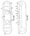
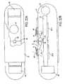
- the sensor 10has as its primary components a sensor body 12; a matrix layer 14 coated over the exterior surface of the sensor body 12, with fluorescent indicator molecules 16 distributed throughout the layer; a radiation source 18, e.g. an LED, that emits radiation, including radiation over a range of wavelengths which interact with the indicator molecules (referred to herein simply as "radiation at a wavelength which interacts with the indicator molecules"), i.e., in the case of a fluorescence-based sensor, a wavelength which causes the indicator molecules 16 to fluoresce; and a photosensitive element 20, e.g.
- indicator molecules 16could simply be coated on the surface of the sensor body.
- the indicator moleculesare contained within the matrix layer 14, which comprises a biocompatible polymer matrix that is prepared according to methods known in the art and coated on the surface of the sensor body as explained below.
- Suitable biocompatible matrix materialswhich must be permeable to the analyte, include methacrylates and hydrogels which, advantageously, can be made selectively permeable -- particularly to the analyte -- i.e., they perform a molecular weight cut-off function.
- the sensor 12advantageously is formed from a suitable, optically transmissive polymer material which has a refractive index sufficiently different from that of the medium in which the sensor will be used such that the polymer will act as an optical wave guide.
- Preferred materialsare acrylic polymers such as polymethylmethacrylate, polyhydroxypropylmethacrylate and the like, and polycarbonates such as those sold under the trademark Lexan®.
- the materialallows radiation employed by the deviceradiation generated by the radiation source 18 (e.g., light at an appropriate wavelength in embodiments in which the radiation source is an LED) and, in the case of a fluorescence-based embodiment, fluorescent light emitted by the indicator molecules-- to travel through it.
- radiatione.g., light
- the radiation source 18is emitted by the radiation source 18 and (at least some) is reflected internally at the surface of the sensor body 12, e.g., as at location 22, thereby "bouncing" back-and-forth throughout the interior of the sensor body 12.
- the fluorescent, indicator molecules 16enters the sensor body 12, either directly or after being reflected by the outermost surface (with respect to the sensor body 12) of the matrix layer 14, as illustrated in region 30.
- Such fluorescent light 28is then reflected internally throughout the sensor body 12, much like the radiation emitted by the radiation source 18 is, and, like the radiation emitted by the radiation source, some will strike the interface between the sensor body and the surrounding medium at angles too small to be reflected and will pass back out of the sensor body.
- Internal reflection of radiation emitted by the source 18 and, for fluorescence-based sensors, fluorescent light emitted by the fluorescent indicator molecules 16, illustrated schematically in Figure 4impinges on the photosensitive element 20, which senses the level of such internal illumination.
- the senor 10may also include reflective coatings 32 formed on the ends of the sensor body 12, between the exterior surface of the sensor body and the matrix layer 14, to maximize or enhance the internal reflection of the radiation and/or light emitted by fluorescent indicator molecules.
- the reflective coatingsmay be formed, for example, from paint or from a metallized material (provided such metallized material does not impede transmission of telemetry signals to and from the sensor, described below).
- an optical filter 34preferably is provided on the light-sensitive surface of the photosensitive element (photodetector) 20.
- This filterprevents or substantially reduces the amount of radiation generated by the source 18 from impinging on the photosensitive surface of the photosensitive element 20.
- the filterallows fluorescent light emitted by fluorescent indicator molecules to pass through it to strike the photosensitive region of the detector. This significantly reduces "noise" in the photodetector signal that is attributable to incident radiation from the source 18.
- the application for which the sensor 10 according to one aspect of the invention was developed in particular -- although by no means the only application for which it is suitable --is measuring various biological analytes in the human body, e.g., glucose, oxygen, toxins, pharmaceuticals or other drugs, hormones, and other metabolic analytes.
- the specific composition of the matrix layer 14 and the indicator molecules 16may vary depending on the particular analyte the sensor is to be used to detect and/or where the sensor is to be used to detect the analyte (i.e., in the blood or in subcutaneous tissues).
- the matrix layer 14facilitate exposure of the indicator molecules to the analyte and that the optical characteristics of the indicator molecules (e.g., the level of fluorescence of fluorescent indicator molecules) are a function of the concentration of the specific analyte to which the indicator molecules are exposed.
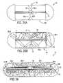
- the senor 10is formed in a smooth, oblong or rounded shape.
- ithas the approximate size and shape of a bean or a pharmaceutical gelatin capsule, i.e., it is on the order of approximately 500 microns to approximately 0.5 inch in length L and on the order of approximately 300 microns to approximately 0.3 inch in diameter D, with generally smooth, rounded surfaces throughout.
- This configurationpermits the sensor 10 to be implanted into the human body, i.e., dermally or into underlying tissues (including into organs or blood vessels) without the sensor interfering with essential bodily functions or causing excessive pain or discomfort.
- the "foreign body response”is most often fibrotic encapsulation, i.e., the formation of scar tissue.
- Glucose -- a primary analyte which sensors according to the invention are expected to be used to detect --may have its rate of diffusion or transport hindered by such fibrotic encapsulation.
- molecular oxygen (O 2 )which is very small, may have its rate of diffusion or transport hindered by such fibrotic encapsulation as well. This is simply because the cells forming the fibrotic encapsulation (scar tissue) can be quite dense in nature or have metabolic characteristics different from that of normal tissue.
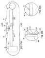
- a sensor/tissue interface layer -- overlying the surface of the sensor body 12 and/or the indicator molecules themselves when the indicator molecules are immobilized directly on the surface of the sensor body, or overlying the surface of the matrix layer 14 when the indicator molecules are contained therein -is prepared from a material which causes little or acceptable levels of fibrotic encapsulation to form.
- Two examples of such materials described in the literature as having this characteristicare PrecludeTM Periocardial Membrane, available from W.L. Gore, and polyisobutylene covalently combined with hydrophiles as described in Kennedy, "Tailoring Polymers for Biological Uses," Chemtech, February 1994, pp. 24-31 .
- the sensor/tissue interface layer 36may include three sublayers 36a, 36b, and 36c.
- the sublayer 36aa layer which promotes tissue ingrowth, preferably is made from a biocompatible material that permits the penetration of capillaries 37 into it, even as fibrotic cells 39 (scar tissue) accumulate on it.
- Gore-Tex® Vascular Graft materialePTFE
- Dacron®PET
- MEDPOR Biomaterial produced from high-density polyethyleneavailable from POREX Surgical Inc.
- materialswhose basic composition, pore size, and pore architecture promote tissue and vascular ingrowth into the tissue ingrowth layer.
- the sublayer 36bpreferably is a biocompatible layer with a pore size (less than 5 micrometers) that is significantly smaller than the pore size of the tissue ingrowth sublayer 36a so as to prevent tissue ingrowth.
- a presently preferred material from which the sublayer 36b is to be madeis the Preclude Periocardial Membrane (formerly called GORE-TEX Surgical Membrane), available from W.L. Gore, Inc., which consists of expanded polytetra-fluoroethylene (ePTFE).
- the third sublayer 36cacts as a molecular sieve, i.e., it provides a molecular weight cut-off function, excluding molecules such as immunoglobulins, proteins, and glycoproteins while allowing the analyte or analytes of interest to pass through it to the indicator molecules (either coated directly on the sensor body 12 or immobilized within a matrix layer 14).
- a molecular weight cut-off functionexcluding molecules such as immunoglobulins, proteins, and glycoproteins while allowing the analyte or analytes of interest to pass through it to the indicator molecules (either coated directly on the sensor body 12 or immobilized within a matrix layer 14).
- Many well known cellulose-type membranese.g., of the sort used in kidney dialysis filtration cartridges, may be used for the molecular weight cut-off layer 36c.
- the sensor/tissue interface layer 36is described and shown in Figure 3 as including a third, molecular weight cut-off layer 36c, it will be appreciated that it is possible to select a polymer from which to make the matrix layer 14, e.g., a methacrylate or a hydrated hydrophilic acrylic, such that it performs the molecular weight cut-off function without the need for a separate sublayer 36c. It is recommended, however, that the two sublayers 36a and 36b be used, with the outer layer 36a promoting tissue ingrowth and the inner layer 36b preventing tissue ingrowth, because the inner layer 36b functions as an additional barrier (or "prefilter") between the outer layer 36a and the molecular weight cut-off layer (whether provided separately or by the matrix layer 14 itself).
- a polymer from which to make the matrix layer 14e.g., a methacrylate or a hydrated hydrophilic acrylic
- the analyte exposure lag timei.e., the amount of time it takes for the concentration of analyte to which the indicator molecules are directly exposed to come to a steady state, must be relatively short, i.e., on the order of two to five minutes.
- the interface layerenhances reflection of light (whether from fluorescent indicator molecules or from the radiation source 18) from the outermost surface of the matrix layer 14 and into the sensor body 12.
- a further aspect of a sensor according to the inventionis that it may be wholly self-contained.
- the sensormay be constructed in such a way that no electrical leads extend into or out of the sensor body to supply power to the sensor (e.g., for driving the source 18) or to transmit signals from the sensor.
- a sensor according to this aspect of the inventionmay include a power source 40 ( Figure 1 ) that is wholly embedded or encapsulated within the sensor body 12 and a transmitter 42 ( Figure 1 ) that also is entirely embedded or encapsulated within the sensor body 12.
- the power source 40is an inductor, as is the transmitter 42.
- the sensorwhen the sensor is implanted in the body, e.g. between the skin 50 and subcutaneous tissues 52 as shown in Figure 5 , the sensor can be powered -- i.e., the radiation source can be caused to emit radiation which interacts with the indicator molecules 16 -- by exposing the sensor to a field of electromagnetic radiation 54 created, for example, by an inductor coil 56 that is housed in an appropriately configured instrument (not shown) positioned near the sensor.
- the transmitter 42as an inductor, generates an electromagnetic field 58 that is indicative of the level of light striking the photosensitive element and hence the presence or concentration of analyte.
- the field 58constitutes a signal that can be detected by an external receiver 60.
- the signalmay be, for example, a 50 megahertz carrier, amplitude modulated signal; a frequency modulated signal; a digital signal; or any other type of electromagnetic wave signal that would be known to one having skill in the art.
- the coil 56generates the electromagnetic wave 54 at one frequency to induce a current in the inductor 40, which powers the source of radiation 18; the amount of internally reflected light sensed by the photosensitive element 20 is transmitted by the same inductor 40 as a modulated electromagnetic wave which induces a current in coil 56.
- This modulated waveis generated by modulating the current flowing through inductor 40 by the photosensitive element 20 as a function of detected light and is detected by measuring the resulting induced current in coil 56.
- the systemcould be configured to switch (in rapid sequence) between a power generating mode and a signal transmitting mode.
- microbatterieswhich generate a voltage when exposed to mechanical energy such as ultrasonic found
- micro generatorse.g., ultrasound
- photovoltaic cellswhich can be powered by light (infrared) passing through the skin 50.
- a radioluminescent light sourcein place of an LED, can be used.
- a radioluminescent light sourceincludes a sealed, optically transmissive vessel 80 (e.g., cylindrical, spherical, or cubic) with a sample of radioisotope 82, e.g. tritium, contained therein.
- the radioisotopeemits beta particles which strike intermediate luminophore molecules 84 coated on the interior surface of the vessel 80, thereby causing the intermediate luminophore molecules to emit light.
- the beta particlesare too weak to pass through the walls of the vessel, the light emitted by the intermediate luminophore molecules does pass through, thereby illuminating the sensor with light - similarly to an LED -- that interacts with the indicator molecules.
- radioluminescent generation of light, and similar generation of lightis known in the art. See, for example, U.S. Patent No. 4,677,008 , the disclosure of which is incorporated by reference, and Chuang and Arnold, "Radioluminescent Light Source for Optical Oxygen Sensors," 69 Analytical Chemistry No. 10, 1899-1903, May 15, 1997 , the disclosure of which also is incorporated by reference.
- the sensormight employ an electroluminscent lamp such as that shown in U.S. Patent No. 5,281,825 .
- a temperature sensor 64 and an optional signal amplifier 66are also advantageously provided.
- the temperature sensor 64measures the locally surrounding temperature of the ambient tissues and the indicator molecule environment and provides this information to the control logic circuit (not shown).
- the control logic circuitcorrelates fluorescence level, for example, with analyte concentration level, thereby correcting the output signal for variations affected by temperature.
- Amplifier 66is a relatively simple gain circuit which amplifies the signal generated by the photodetector 20.
- the various components and circuitry of the sensorare assembled onto a precut, 0.2 inch by 0.4 inch ceramic (e.g., alumina) substrate 70.
- the substrate thicknessis 0.020 inch.
- All circuit elementsare standard surface mount components available, e.g., from Digi-Key, Garrett, and others.
- the componentsare attached to the substrate using standard silver conductive epoxy such as Ablebond-84, available from Ablebond.
- a high pass filtermay be installed on the photosensitive element by applying a two-part high pass filter epoxy, commonly available from CVI Laser and others. Thickness of the filter is controlled by precision dispensing using a Rainin Micropipettor. The high pass filter epoxy is cured in an oven at 125°C for two hours, as per the manufacturer's instructions.
- a low pass filtermay be coated over the radiation source (LED) by the same method using a commercially available low pass epoxy formulation. Custom formulations of optical filters can be prepared by adding a dye of the desired absorption spectra into Epotek epoxies.
- the appropriate concentration of the dopantcan be determined by monitoring wavelength versus transmittance on a UV-Vis scan from a spectrophotometer until the desired spectral properties are obtained.
- Such custom-formulated epoxiescan be cured similarly.
- Prefabricated glass, polymer, or coated filtersmay also be used and simply glued to the photosensitive element or devices using an optically matching adhesive, as is typical.
- the circuit board with optical filters(if installed and cured) is then encapsulated using, e.g., a Lilly No. 4 two-part gelatin capsule as a mold. Other gelatin capsules work as well.
- the long "half" of an empty capsuleis placed upright into a rack.
- Several drops of optically clear potting of the appropriate sensor body material, as described above,are added to fill the capsule to approximately one half of its volume.
- the substrate with pre-assembled circuitryis inserted end-on into the capsule and into the optical potting, which wicks around and into the small spaces of the circuit board assembly to help exclude air and thus prevent bubbles from subsequently forming in the finished sensor device.
- Additional optical pottingis added using a micropipettor until the level reaches the top of the capsule with the capsule standing upright.
- the partial assemblyis then further degassed by placing the capsule (supported by the rack) under a bell jar vacuum and allowing it to stand under vacuum until any bubbles observed within the capsule have escaped.
- the assemblyis removed from the vacuum and "topped off' with additional optical potting, allowing surface tension to fill the gelatin capsule half above its rim and to create a rounded, hemispherical dome shape that is similar to the opposite end.
- the capsuleis then placed under UV light and cured for several hours, with the curing time depending on the intensity of the UV source available.
- Heat cure and catalyst curemay alternatively be used, depending on the potting material.
- a full strength cureis obtained by subsequently incubating the post-UV-cure assembly at 60°C for 12 hours, or otherwise as per the manufacturer's instructions.
- the gelatin moldis then removed from the sensor body by soaking the encapsulated assembly in water for several hours to dissolve the gelatin. Several water changes and washes over the course of the time period help to remove all of the gelatin from the surface.
- the capsuleis then air dried (or oven dried at 60°C) in preparation for coating.
- the indicator moleculesmay be immobilized directly on the surface of the sensor body using techniques known in the art, or they may be contained within a matrix layer solution that is coated onto the central body.
- a matrix layer solution containing fluorescent indicator moleculesmay be prepared according to methods known in the art; a matrix layer solution containing light-absorbing indicator molecules may be prepared as described below.
- a convenient method for coating the sensor with a matrix layeris to affix a small (e.g., 32 gauge) wire to one end of the encapsulated circuitry to produce a hanger. This can be done using the same UV-cured optical potting material. Approximately one to two microliters of optical potting is placed on the end of the handle wire.
- the encapsulated circuitis placed in front of a UV lamp with the UV lamp turned off.
- the wire with optical potting on the tipis touched to the end of the capsule and the lamp is turned on.
- the small amount of optical potting "adhesive"will be cured immediately, thereby attaching the wire tip to the capsule.
- the capsulemay now be dipped conveniently into matrix layer solutions (and separate indicator molecule solutions, as appropriate) and hung by the wire to cure.
- the wiremay be removed simply by pulling it after the sensor is completely assembled.
- the sensor/tissue interface layeris constructed by inserting the sensor body into a preformed tubular sleeve of the material and sealing each end using heat or epoxy or, if the desired sensor/tissue interface layer material is in sheet form, by rolling the sensor body longitudinally in the material and sealing the longitudinal seam and end seams using heat or epoxy.
- a sensor 10has a single radiation source 18 (LED) and photosensitive element 20 (photodetector), thereby permitting detection of a single analyte
- LEDradiation source
- photosensitive element 20photodetector
- two or more different types of indicator moleculesmay be provided to sense the presence or concentration of two or more analytes, respectively, with two or more photosensitive elements being provided on the ceramic substrate 70, each with its own respective transmitter 42.
- Each photosensitive elementwould have its own filter 34 designed to allow light from the respective indicator molecules to pass through to it.
- a "two-channel" embodimentcould be developed to measure analyte concentration by two different sensing schemes.
- some of the indicator moleculeswould be fluorescent indicator molecules and the rest of the indicator molecules would be radiation-absorbing indicator molecules (as described below).
- Two separate photosensitive elementswould be provided, each with its own appropriate filter -- one to measure fluorescent light emitted by the fluorescent indicator molecules and one to measure radiation generated by the source and reflected throughout the sensor, with some absorption by the radiation-absorbing indicator molecules.
- other types of photosensitive elementsmay be used, e.g., photoresistors, phototransistors, photodiodes, photodarlingtons, photovoltaic cells, positive insulating negative photodiodes, large-area photodiodes, avalanche photodiodes, charge coupled devices, etc.
- a sensor according to the inventionhas been described above primarily as functioning based on fluorescence of indicator molecules, the invention is not so limited.
- a sensor construct as per the inventionmay operate based on the light-absorbing characteristics of light-absorbing indicator molecules.
- a sensor according to this aspect of the inventioncould use a sensor construct like that shown in U.S. Patent No. 5,517,313 , referenced above; more preferably, it uses a bean- or pharmaceutical gelatin capsule construct as described above.
- the light-absorbing indicator molecules 116(which preferably are immobilized in a matrix layer 114) absorb a certain amount of radiation (light) 119 generated by the radiation source, falling within a particular range of wavelengths and passing out of the sensor body, and non-absorbed radiation 121 is reflected back into the sensor body.
- the sensor 110is exposed to analyte such that the light-absorbing indicator molecules 116 are exposed to analyte molecules 117, the light-absorbing properties of the indicator molecules are affected.
- the light-absorbing capacity of the indicator molecules 116may decrease such that the intensity of the light 121 reflected back into the sensor body 12 increases.
- the level of light within the sensor bodyis measured by a photosensitive element (not shown), as described above.
- a light-absorbing indicator molecule-based sensormust be calibrated by determining the illumination intensity levels for various known concentrations of various analytes of interest. Furthermore, because the radiation (light) being measured is the radiation being emitted by the source itself, it will be further appreciated that if the radiation source has a very broad emission profile and the light-absorbing indicator molecule has a very narrow range of absorption wavelengths, a high-pass, low-pass, or band-pass filter may be provided over the photosensitive element so as to permit only this range of radiation wavelengths to be sensed by the photosensitive element.
- Indicator moleculeswhose light-absorbing properties are affected by various analytes are known in the art. (As noted above, however, it is believed that such light-absorbing indicator molecules have not been used in connection with a sensor construct either like that taught herein or in U.S. Patent No. 5,517,313 .)
- U.S. Patent No. 5,512,246discloses light-absorbing indicator molecules whose ability to absorb light varies as a function of the local concentration of glucose. In particular, as the local concentration of glucose increases, the ability of the indicator molecules to absorb light at a wavelength of 515 nanometers decreases. Therefore, if such indicator molecules are used in connection with a bean- or cold capsule-shaped sensor construct as disclosed herein, the level of internal illumination by light at that wavelength will increase. The local glucose concentration level can then be determined from the level of illumination at that wavelength.
- Light-absorbing indicator moleculeswhich are responsive to other analytes are well known in the art, e.g., as exemplified by phenolphthalein, which changes color in response to a change in pH.
- a sensor which utilizes light-absorbing indicator moleculescould have the indicator molecules disposed directly on the surface of the sensor body. It is preferred, however, that the indicator molecules be immobilized within a matrix layer 114, as is shown in Figures 7a and 7b .
- the matrix layer 114may be manufactured by the low density polymerization of various organic monomers, including hydroxethylmethacrylate (HEMA).
- HEMAhydroxethylmethacrylate
- HEMAis widely available from sources such as PolyScienses in Warrington, Pennsylvania and Sigma in St. Louis, Missouri, and may be polymerized by means of heating or exposing the monomers to ultraviolet light, as widely known and understood in the art.
- the light-absorbing indicator molecules 116are immobilized within the matrix layer 114 by reacting the HEMA with a doped monomer, e.g., aminoethylmethacrylate (AEMA).
- AEMAaminoethylmethacrylate
- AEMAintroduces a pendant amine group into the matrix layer 114.
- Monomers other than AEMAalso may be used during the manufacture of the matrix layer 114, including aminopropylmethacrylate (APMA) and other commercially available monomers having different pendant groups and varying carbon chain lengths between the amino group and the rest of the monomer.
- APMAaminopropylmethacrylate
- monomers containing secondary amine groupsalso may be used for forming the matrix layer 114.
- pendant cross-linker groups other than amine groupsalso may be used to covalently link the indicator molecules 116 to the polymer material of the matrix layer 114.
- Examples of alternative pendant cross-linker groupsinclude sulfhydryl (-SH), carboxyl (COOH), aldehyde (COH), hydroxyl (OH), cyano (CN), ether, and epoxyl groups.
- the matrix layer 114is provided so as to have stoichiometrically one pendant amino group for every three HEMA residues in the overall polymerized macromolecule of the matrix layer 114. This is illustrated by the formula in Figure 8 .
- the polymer material of the matrix layer 114may be cross-linked by standard cross-linking methods known in the art, including in a preferred embodiment a method using as a cross-linker group a bifunctional poly(ethylene glycol) (n) dimethacrylate.
- the cross-linker groupmay be added as per standard practice during the initial formulation of the monomer. This and other cross-linker groups are commercially available from PolySciences (Warrington, Pa.).
- the variable (n)may vary depending on the desired density, porosity, and hydrophilic properties of the matrix layer 114.
- Figure 9illustrates a segment of the matrix layer 114 in accordance with a preferred embodiment of the present invention, which includes a pendant amino doped monomer (AEMA), a HEMA backbone, and a bifunctional cross-linker group.
- AEMApendant amino doped monomer
- the matrix layer 114offers several advantages to the present invention, including allowing access of the analyte (e.g., glucose) to the light-absorbing indicator molecules 116; immobilizing the indicator molecules 116 to prevent them from leaching; maintaining the stability of the optical system of the invention; minimizing the amount of non-specific binding to the porous matrix of molecules other than the desired analyte; restricting access of molecules larger than the desired analyte; and permitting the porous matrix material to support one or more additional, biocompatible interface layers.
- the matrix layer 114also is optically compatible with the sensor body 12 and is able to transmit excitation, emission, absorbance, or refractive index wavelength(s) of the indicator molecules 116.
- the indicator molecule 116is a glucose-sensitive, absorbance-modulated indicator molecule which may be covalently immobilized within the matrix layer 114. During polymerization, the indicator molecule 116 covalently attaches to the polymer backbone through a primary amine pendant group, and together they form the matrix layer 114. This form of immobilization is adaptable to various methods using different types of indicator molecules and different pendant groups on the polymer backbone. Examples of glucose-sensitive, absorbance-modulated indicator molecules include 2,3'-dihydroxyboron-4-hydroxy-azobenzene (also known as "Boronate Red"), as depicted in Figure 10 . Glucose can interact with the indicator molecules 116, as described in U.S. Patent No. 5,512,246 . Another similarly prepared preferred indicator molecule 116 for use in the present invention is depicted in Figure 11 .
- the ortho hydrogen position of the phenol group(represented by an "*" in the indicator molecules depicted in Figures 10 and 11 ) is aminoalkylated using the Mannich reaction, which is known in the organic chemistry art as a reaction wherein certain hydrogens ofketones, esters, phenols, and other organic compounds may be condensed in the presence of formaldehyde and an amine.
- the reagents for performing the Mannich reactionare commercially available from many chemical supply companies, including Pierce Chemicals.
- a standard Mannich reaction for linking the indicator molecule 116 to AEMAis depicted in Figure 12 .
- the indicator molecule 116may be linked to the polymer material of the matrix layer 114 in various ways, including first coupling the indicator molecule 116 to AEMA prior to co-polymerization with HEMA. Alternatively, non-covalent, mechanical entrapment of the indicator molecule 116 may be used by first immobilizing the indicator molecule 116 to pendant amine groups of polylysine. The preimmobilized polylysine/indicator molecule precursor can then be mixed with HEMA prior to polymerization. Upon polymerization of the methacrylate, the polylysine/indicator molecule complex is trapped within the methacrylate matrix, while at the same time the indicator molecule 116 remains covalently immobilized to polylysine.
- the sensor 110otherwise is constructed as described above.
- a sensor according to a third aspect of the inventiontakes advantage of the bean- or cold capsule-shaped construct described above (although by no means is limited to such a construct) to facilitate sensing the presence or concentration of an analyte based on changes in the refractive index of the medium in which the sensor is disposed (or the refractive index of a matrix encapsulating the sensor, if one is used).
- the critical anglewill be 90° (i.e., tangent to the interface between the sensor body and the surrounding medium), and therefore all light generated by the source 18 will pass out of the sensor body 12 and none (or almost none) will be sensed by the photosensitive elements 20.
- the refractive index of a mediumincreases with the density of the medium.
- the density of the membranewill increase as analyte diffuses into it. This allows more light to pass out of the sensor body and causes less light to strike the photosensitive elements.
- the level of internal reflectionwill decrease, and this decrease can be measured and correlated to the local analyte concentration.
- Glucose, salts, and other small molecular weight compoundsare the primary metabolic analytes which will diffuse into the membrane and therefore are the analytes a refraction-based sensor could be used most effectively to measure.
- a surrounding membranewould not need to be used.
- Such a basic embodimentcould be used where the only matter varying in concentration is the analyte of interest. For example, as champagne or wine ages, the sugar content decreases, as does the density and hence the refractive index of the fluid. Therefore, a sensor according to this aspect of the invention could be placed in a bottle of champagne or a cask of wine as it is processing and used to measure sugar content as the champagne or wine develops. Other potential applications are determining the liquid level inside a vessel or determining the amount of moisture in fuel oil.
- a sensorwhich includes: (a) at least one analyte sensing indicator channel that operates as described above; and (b) at least one additional channel that serves as an optical reference channel.
- the optical reference channelpreferably: (a) measures one or more optical characteristic(s) of the indicator molecule (i.e., the indicator molecule of the analyte sensing indicator channel) which is unaffected or generally unaffected by the presence or concentration of the analyte; and/or (b) measures one or more optical characteristic(s) of a second control indicator molecule which is unaffected or generally unaffected by the presence or concentration of the analyte.
- the optical reference channelcan operate, for example, generally like the indicator channel.
- indicator molecules that are unaffected or generally unaffected by the presence or concentration of an analyteare broadly referred to herein as control indicator molecules.
- the optical reference channelcan be used, for example, to compensate or correct for: (1) changes or drift in component operations intrinsic to the sensor make-up; and/or (2) environment conditions external to the sensor.
- the optical reference channelcan be used to compensate or correct for internal variables induced by, among other things: aging of the sensor's radiation source; changes affecting the performance or sensitivity of a photosensitive element thereof; deterioration or alteration of the indicator molecules; changes in the radiation transmissivity of the sensor body, or of the indicator matrix layer, etc.; changes in other sensor components; etc.
- the optical reference channelcould also be used to compensate or correct for environmental factors (e.g., factors external to the sensor) which could affect the optical characteristics or apparent optical characteristics of the indicator molecules irrespective of the presence or concentration of the analyte.
- environmental factorse.g., factors external to the sensor
- exemplary external factorscould include, among other things: the temperature level; the pH level; the ambient light present; the reflectivity or the turbidity of the medium that the sensor is applied in; etc.
- an indicator membranee.g., such as the membrane 14' described below
- an indicator membranecan include indicator molecules that are sensitive to a particular analyte, such as for instance fluorescent indicator molecules that are sensitive to oxygen, and that are contained within a material that is permeable to that analyte while a reference membrane (e.g., such as the membrane 14" described below) can include the same indicator molecules within a material that is not permeable to that analyte.
- the indicator membranecan have an oxygen permeable matrix containing the indicator molecules in such a manner that oxygen freely passes through and contacts the indicator molecules (in one example, silicon rubber may be employed for the indicator membrane, which is very permeable to oxygen).
- fluctuations in values obtained in the reference channelshould be substantially non-attributable to the presence or concentration of the analyte (e.g., oxygen), but rather to, as described above, for example (1) variables intrinsic to the sensor itself or (2) external environmental factors.
- analytee.g., oxygen
- Materials that are substantially impermeable to an analytecan include, for example: a) materials that substantially prevent penetration of elements (see, as one example, U.S. Patent No. 3,612,866 , discussed below, wherein the reference channel is coated with varnish); and b) perm-selectable membranes, wherein the control indicator molecules are located within a matrix that is perm-selectable such that it allows certain elements to pass while blocking certain other elements such as the particular analyte (as one example, the matrix can allow negatively charged molecules to pass while blocking positively charged molecules).
- the indicator membranecan include indicator molecules that are sensitive to a particular analyte, such as for example fluorescent indicator molecules that are sensitive to glucose, and that are contained within a material that is permeable to that analyte while the reference membrane can also include a material that is permeable to that analyte, but which does not include the same indicator molecules, but rather control indicator molecules that are, in essence, substantially blind to that analyte.
- indicator moleculesthat are sensitive to a particular analyte, such as for example fluorescent indicator molecules that are sensitive to glucose, and that are contained within a material that is permeable to that analyte
- the reference membranecan also include a material that is permeable to that analyte, but which does not include the same indicator molecules, but rather control indicator molecules that are, in essence, substantially blind to that analyte.
- the analyteis glucose and such glucose is within a liquid (such as, for example, body fluids like blood, serum, tissue interstitial fluid, etc., or other fluids)
- a liquidsuch as, for example, body fluids like blood, serum, tissue interstitial fluid, etc., or other fluids
- placing the control indicator molecules within a material that is not permeable to such glucosewould likely have the additional affect of blocking other factors such as changes in pH, etc., so that the first example described above would not be desirable.
- the analyteis allowed to penetrate, but the control indicator molecules selected in the reference channel are chosen so as to be substantially blind to that analyte.
- fluctuations measured by the reference channelshould be substantially unattributable to changes in the presence or concentration of that analyte.
- control indicator moleculesthat are substantially blind to an analyte can be made as follows. First, reference is made to U.S. Patent Application Serial No. 09/265,979, filed on March 11, 1999 , entitled Detection of Analytes by Fluorescent Lanthanide Metal Chelate Complexes Containing Substituted Ligands, also owned by the present assignee, the entire disclosure of which is incorporated herein by reference (and which is a continuation-in-part of application Serial No.
- the '960 applicationdescribes indicator molecules with a fluorescent lanthanide metal chelate complex having the formula: M(--Ch(-R X )) Y wherein: M represents a lanthanide metal ion; Ch represents a chelator comprising a ligand, preferably an organic ligand which can comprise any one or more of a ⁇ -diketone or a nitrogen analog thereof, a dihydroxy, a carboxyl coordinating heterocycle, an enol, a macrobicyclic cryptand ( i.e ., a cage-type ligand), a phenylphosphonic acid, or a polyamino-polycarboxylic acid.
- Mrepresents a lanthanide metal ion
- Chrepresents a chelator comprising a ligand, preferably an organic ligand which can comprise any one or more of a ⁇ -diketone or a nitrogen analog thereof, a dihydroxy, a carboxyl coordinating heterocycle, an en
- the organic ligand of Chcan also comprise any one or more of a heterocycle of nitrogen, sulfur, and linked carboxyls.
- the organic ligand of Chcan further comprise any one or more of an alkane or alkene group, preferably containing 1 to 10 carbon atoms, as well as aromatic, carbocyclic or heterocyclic moieties, including benzyl, napthyl, anthryl, phenanthryl, or tetracyl groups.
- one or more chelators complexed with Mcan be the same or a mixture of different chelators (so-called "mixed ligand or ternary chelates").
- Rrepresents an analyte-specific recognition element, one or more of which is bound to one or more ligands of the chelate complex, but need not be linked to every ligand of the chelate complex.
- Rcan be a boronate group or a compound containing a boronate group for detecting glucose or other cis-diol compound.
- Another method of obtaining separate indicator channel and reference channel readingsinvolves utilizing an indicator molecule having an isosbestic point at a particular wavelength or frequency (e.g., at about 440 nm in the non-limiting example shown for illustrative purposes in FIG. 21 ).
- An "isosbestic point”involves a point (i.e., substantially at a particular wavelength) where the absorptivity, for example, is the same irrespective of the presence or concentration of an analyte.
- the indicator and reference channelswould include indicator molecules having a specific isosbestic point (e.g., the same indicator molecules can be used in each channel).
- the indicator channelcan include a filter (e.g., see filter 34 discussed below) over a photosensitive element (e.g., a photo-detector) 20-1, discussed below, allowing light outside of the isosbestic point to be detected by the photosensitive element (e.g., at, for instance, about 500 nm in FIG. 21 ).
- the reference channelwill include a filter (e.g., 34 below) over a photosensitive element (e.g., a photo-detector) 20-2, discussed below, allowing light substantially at the isosbestic wavelength to penetrate and be detected by the photosensitive element 20-2.
- any variation detected in the reference channelshould be largely irrespective of analyte presence or concentration and can be used as a reference as discussed herein-above.
- Other indicator molecules having such an isosbestic pointcan be used based upon the particular application at hand.
- 5,137,833(showing a glucose indicator with an isosbestic point at about 440 nm, see, e.g., FIG. 10 of the '833 patent reproduced herein at FIG. 21 ) the entire disclosure of which is incorporated herein by reference.
- a radiation sourcee.g., an LED
- a radiation sourcemay not provide sufficient illumination at wavelengths around the isosbestic point such that it may be desirable to include an additional LED to provide sufficient illumination at such wavelengths.
- the reference channels and the indicator channels of the present inventioncan utilize materials as described herein and as known in the art depending on the particular application at hand.
- U.S. Patent No. 3,612,866the entire disclosure of which is incorporated herein by reference, describes a fluorescent oxygen sensor having a reference channel containing the same indicator chemistry as the measuring channel, except that the reference channel is coated with varnish to render it impermeable to oxygen.
- U.S. Patent Nos. 4,861,727 and 5,190,729the entire disclosures of which are also incorporated herein by reference, describe oxygen sensors employing two different lanthanide-based indicator chemistries that emit at two different wavelengths, a terbium-based indicator being quenched by oxygen and a europium-based indicator being largely unaffected by oxygen.
- U.S. Patent No. 5,094,959the entire disclosure of which is also incorporated herein by reference, describes an oxygen sensor in which a single indicator molecule is irradiated at a certain wavelength and the fluorescence emitted by the molecule is measured over two different emission spectra having two different sensitivities to oxygen. Specifically, the emission spectra which is less sensitive to oxygen is used as a reference to ratio the two emission intensities.
- U.S. Patent Nos. 5,462,880 and 5,728,422the entire disclosures of which are also incorporated herein by reference, describe a radiometric fluorescence oxygen sensing method employing a reference molecule that is substantially unaffected by oxygen and has a photodecomposition rate similar to the indicator molecule.
- U.S. Patent No. 4,580,059the entire disclosure of which is incorporated herein by reference, describes a fluorescent-based sensor containing a reference light measuring cell 33 for measuring changes in the intensity of the excitation light source -- see, e.g., column 10, lines 1, et seq.
- U.S. Patent No. 4,617,277the entire disclosure of which is also incorporated herein by reference, describes an absorbance-based sensor for carbon monoxide, in which a reference element 12 reflects light from a source 14 to a reference photocell to determine when a measuring element 10 needs replacement due to irreversible color change.
- the membranes 14' and 14"can both include light-absorbing indicator molecules, such as those described herein-above.
- the indicator and reference membranes 14' and 14"will both use like indicator molecules, such as described herein.
- control channelcould use materials or substances that are completely unrelated to the indicator molecules in the indicator channel.
- the substance of the reference membranecould merely have desirable characteristics with respect to one or more of, as some examples, reflectivity, temperature, pH, and/or various other factors.
- the reference membranecould contain no corresponding "chemistry", but could, for example, be used to just monitor reflectivity (this could be used, for example, to evaluate if an LED dimmed or if, for example, the surface of the membrane was affected in some manner).
- one or more reference channelscan be incorporated in any of the embodiments disclosed in this application.
- a variety of preferred embodiments of sensors incorporating reference indicatorsare discussed herein-below. While some alternatives and variations in the following embodiments are described below, like reference numerals refer to like parts to the previously described embodiments, and all alternatives and variations described herein-above with respect to such like parts can also be employed in any of the following embodiments where appropriate.
- FIGS. 14(A)-14(B)illustrate a first embodiment of a sensor 10 incorporating an optical reference channel.
- the sensor 10preferably includes: a sensor body 12; an indicator membrane 14' having fluorescent indicator molecules distributed throughout the membrane; a reference membrane 14" having fluorescent control indicator molecules distributed throughout the membrane; a radiation source 18, such as for example a single LED similar to that described herein-above; an indicator channel photosensitive element 20-1, made, for example, similar to photosensitive element 20 described herein-above; a similar reference channel photosensitive element 20-2; a circuit substrate 70 (shown schematically with exemplary circuit elements 70i mounted thereto); a power source 40, such as for example an inductive power coil as shown; and a transmitter 42 such as for example a transmitter coil as shown.
- a power source 40such as for example an inductive power coil as shown
- a transmitter 42such as for example a transmitter coil as shown.
- the membranes 14' and 14"can be made, for example, with materials similar to any of the embodiments of the matrix layer 14 discussed above or can comprise any other appropriate materials within which the indicator molecules can be contained or upon which the indicator molecules can be coated.
- the membranes 14' and 14" (and/or the sensor body)can also include, if desired, a sensor/tissue interface layer similar to any of the embodiments of the layer 36, as discussed above.
- This illustrated embodimentcan also include a number of additional elements, such as, for example, as shown: a filter 34 (e.g., to exclude a wavelength or a spectrum of wavelengths of light emitted by an LED, such as blue, and to allow passage of a wavelength or a spectrum of wavelengths of light emitted by the fluorescent material, such as red) ; a baffle 130 (e.g., to inhibit "cross-talk" of light radiated from the indicator channel and the reference channel); a mask 35 surrounding the aperture to each of the photosensitive elements; and/or a temperature sensor 64 (e.g., as described above).
- a filter 34e.g., to exclude a wavelength or a spectrum of wavelengths of light emitted by an LED, such as blue, and to allow passage of a wavelength or a spectrum of wavelengths of light emitted by the fluorescent material, such as red
- a baffle 130e.g., to inhibit "cross-talk" of light radiated from the indicator channel and the reference channel
- the senor 12can function similar to that described above with reference to the embodiments shown in FIGS. 1-13 . However, two separate sensory readings are obtained to provide: a) an indicator reading (via the channel including the indicator membrane 14' and the photosensitive element 24-1); and b) a reference reading (via the channel including the reference membrane 14" and the photosensitive element 20-2). Then, the reference reading can be used, for example, to provide more accurate sensor readings.
- the power source 40causes the radiation emitter 18, e.g., an LED, to emit radiation.
- the radiationtravels within the sensor and reaches both the indicator membrane 14' and the reference membrane 14" (as shown generally by arrows).
- the molecules within these respective membranesexcite, e.g., fluoresce, and light is radiated therefrom (as also shown by arrows) and received by the respective photosensitive elements 20-1 and 20-2.
- This operationis essentially like that described with reference to embodiments described herein-above and is thus not repeated.
- a baffle 130can be included.
- the baffleis preferably impervious to radiation that could affect the photosensitive elements -- e.g., painted black or the like.
- a single radiation sourcee.g., an LED, can be used for both of the "channels.”
- one exemplary method of making the device shown in FIGS. 14(A)-14(B)can be as follows. Initially, an alumina ceramic substrate, which can readily be fabricated by a large number of vendors, can be provided for the circuit substrate 70.
- inductorsfor example, can be provided as the power source 40 and the transmitter 42.
- the inductors and discreet componentscan be electrically connected to the substrate, such as using commonly available solder paste or conductive epoxy.
- other electronic componentscan be attached thereto using, for example, a conductive epoxy, such as in one preferred example ABLEBOND 84 from Ablestick Electronic Materials. Then, the components can be wire bonded to complete the circuit connections.
- Silicon photo-diodessuch as for example part no. 150-20-002 from Advanced Photonics, Inc., are preferably provided as the photosensitive elements 20-1 and 20-2, and are preferably flip chip mounted using ball bonds and conductive epoxy.
- the edges of the photosensitive element apertures in the substrateare preferably masked with a black, non-transparent and non-conductive material, such as, for example, E320 from Epoxy Technology, Inc.
- An optical filter materialsuch as, for example, LP-595 from CVI Laser Corp., is preferably placed in the photo-diode apertures (e.g., apertures cut within the substrate 70) to attenuate light from the radiation source and/or to attenuate ambient light.
- the radiation source employedcan be, for example, an LED that emits light in the blue or ultra-violet bands.
- this circuit assembly structureis preferably molded into an optically transparent encapsulant.
- the encapsulantcan help serve as a waveguide and can also provide environmental protection for the circuitry.
- the indicator and reference sensing membranescan be attached inside pockets in the capsule (e.g., inside depressions in the periphery of the capsule). This attachment can be accomplished, for example, by molding pockets into the capsule and then placing the sensing membranes therein, or by placing the indicator membranes into the mold prior to encapsulation so that pockets are formed around the membranes during encapsulation.
- thisis just one preferred method of construction and the device can be constructed in a variety of ways.
- the embodiments shown hereinhave only two channels (i.e., an indicator channel and a reference channel), other embodiments could contain multiple indicator and/or multiple reference channels.
- FIGS. 14(A)-14(B)can be modified in a variety of ways.
- the devicecan be modified so that a circuit board 70 is fixed to a flexible circuit (e.g., a cable) as shown, such as via electrical leads or contacts 71.
- a circuit board 70is fixed to a flexible circuit (e.g., a cable) as shown, such as via electrical leads or contacts 71.
- a flexible circuite.g., a cable
- the circuitrydoes not necessarily need to be fully encapsulated within the bean.
- the sensor 10can include, as shown, an outer cover 3' and an encapsulating waveguide portion 12' formed within, for example, the illustrated, cross-hatched, region between the photosensitive elements and the indicator and reference membranes.
- the interior of the sensor 10could also include a cavity for the circuitry that contains a gas such as, for example, air, or even a liquid or another medium through which light, e.g., photons, of desired wavelengths can travel.
- a waveguide materialis provided that has a refractive index that matches or is near the refractive index of the material of the indicator and reference membranes so as to ensure travel of light from the membranes to the photosensitive element.
- the waveguide portion 12'can be made from a PMMA material (i.e., poly(methyl methacrylate))
- the circuit board 70can be made with a ceramic material
- the reference coating 14"can contain Ru (ruthenium) in an epoxy
- the indicator coating 14'can contain Ru in silicone
- the baffle 130can be made with a black epoxy material
- the radiation source 18can be an LED
- the outer cover 3'can be made with a glass material.
- FIG. 14(D)is a perspective view of a sensor 10 similar to that shown in FIG. 14(C) , with like numerals indicating like parts.
- FIGS. 14(E) and 14(F)show widthwise and lengthwise cross-sections of the embodiment shown in FIG. 14(D) with the device inserted in a medium B (e.g., liquid, gas, etc.).
- a medium Be.g., liquid, gas, etc.
- the flexible circuit or cable 70'can be made to extend from an outer surface of the medium B to a remote power-source, receiver or other device (not shown) as discussed above.
- the sensor body 12can include an encapsulating waveguide material, such as described above, or an encapsulating waveguide material can be in a region 12' like that shown in FIG. 14(C) , or, although less preferred, another substance can be used as described above.
- FIGS. 15(A)-15(B)show an additional embodiment of the invention which is similar to that shown in FIGS. 14(A)-14(B) , wherein the radiation source 18 is provided as two separate radiation sources, e.g., LEDs, 18-1 and 18-2 that are supported on a mount 18m. As shown, the LED 18-1 is directed toward the indicator membrane 14', while the LED 18-2 is directed towards the reference membrane 14". As shown, a baffle 130 is once again preferably included, in this case between the LEDs. Because multiple radiation sources, e.g., LEDs, are used in this embodiment, the radiation sources, e.g., LEDs 18-1 and 18-2, can be the same, e.g., emit the same light, or can be different depending on circumstances.
- the radiation sources 18-1 and 18-2can be the same, e.g., emit the same light, or can be different depending on circumstances.
- a plurality of radiation sourcese.g., LEDs
- certain considerationsare preferably addressed.
- one radiation sourcee.g., LED
- aging or other factors thereincan more likely equally affect both channels.
- plural radiation sourcese.g., one for each channel
- differences in radiation sourcescan create some discrepancies between channels. Accordingly, in such cases, it is desirable to: a) take steps to provide similar radiation sources (e.g., LEDs) for each channel; and/or b) to calibrate the radiation sources (e.g., LEDs) to one another.
- the LEDsare preferably selected from adjacent LEDs within the rectangular wafer or preferably from within a small distance from one another in the array (e.g., within about a half an inch, or more preferably within about a quarter of an inch, or more preferably within about an eighth of an inch, or more preferably within about a sixteenth of an inch) to be cut from the wafer.
- the qualities of the selected LED chipsshould be more likely analogous to one another.
- a plurality of radiation sourcese.g., LEDs
- a plurality of sourcescan facilitate illumination at desired locations; and/or b) a plurality of sources can, in some cases, be toggled back and forth to reduce cross-talk between channels, as discussed below.
- the device shown in FIGS. 15(A)-15(B)can be used, for examples, in the same manner as the device shown in FIGS. 14(A)-14(B) .
- the two radiation sources, e.g., LEDs, 18-1 and 18-2can also be operated so as to alternate emissions back and forth between the respective LEDs.
- the LED 18-1can be activated for a fraction of a second
- the LED 18-2can be activated for a fraction of a second, etc., with one LED remaining off during the short interval that the other is on. In that manner, cross-talk can be substantially reduced.
- the devicecan be adapted to provide a time delay between readings for the indicator channel and the reference channel (e.g., the indicator membrane could have pico-second decay while the reference membrane could have a nano-second decay, or vise-verse, such that separate channel readings can be made due to temporal differences in radiation emissions).
- the indicator membranecould have pico-second decay while the reference membrane could have a nano-second decay, or vise-verse, such that separate channel readings can be made due to temporal differences in radiation emissions).
- FIG. 15(B)shows the LEDs with central axes each at angles ⁇ of about 25 degrees from the generally horizontal upper surface of the substrate 70
- these anglescan be selected as desired and can vary, as just some examples, between about 0 to 90 degrees depending on circumstances. In some preferred embodiments, for example, the angles ⁇ are about 60 degrees or less, or alternatively about 45 degrees or less.
- FIGS. 15(A)-15(B)can be modified in a variety of ways, similar to the embodiment shown in FIGS. 14(A)-14(B) .
- FIG. 15(C)illustrates that modifications like that shown in FIG. 14(C) can also be made, such as by: (a) including a flexible circuit (e.g., a cable) as shown, such as via electrical leads or contacts 71; (b) providing the sensor 10 with either a fully encapsulated interior, or with a partially encapsulated interior with an encapsulant waveguide portion 12° formed therein; (c) etc.
- a flexible circuite.g., a cable
- a waveguide portion 12'can be made from a PMMA encapsulant material
- a circuit board 70can be made with a ceramic FR4 circuit card
- a radiation source 18can include two LEDs
- a mount 18mcan be a Cu (copper) LED mount
- an outer cover 3'can be made with a glass material.
- a low index layer 12"is also provided over the filters 34 above the photosensitive elements 20-1 and 20-2.
- the indicator membrane 14' and the reference membrane 14"can be formed within a pocket or the like at in the surface of the body 12.
- the membranes 14' and 14"could also be formed on the surface of the body 12 and not within a pocket or the like.
- the use of a pocket or the likecan help protect the membranes 14' and 14" in use and/or prevent the membranes from bulging outward from the side of the body (e.g., eliminating bulges can facilitate handling such as, for example, if the sensor is inserted into a patient via a trocar tube or the like).
- the sensor 10can also include a sensor/tissue interface layer 36 thereover or partially thereover (and/or over the membranes 14' and 14") made, for example, with bio-compatible materials, e.g., such as any materials described herein.
- FIGS. 16(A)-16(B)show an additional embodiment of the invention which is similar to that shown in FIGS. 15(A)-15(B) , wherein the radiation source 18 is provided as two separate radiation sources, e.g., LEDs, 18-1 and 18-2 that are supported on mounts 18ml and 18m2 on opposite sides of the circuit board 70, respectively. As shown, the LED 18-1 is directed toward the indicator membrane 14', while the LED 18-2 is directed towards the reference membrane 14". In this manner, for example, the circuit board 70 can actually operate as a baffle to reduce or eliminate cross-talk. As with the embodiments shown in FIGS. 15(A)-15(C) , the angle ⁇ can be selected as desired and is preferably between about 0 and 90 degrees -- and is in some preferred embodiments less than about 45 degrees.
- the radiation source 18is provided as two separate radiation sources, e.g., LEDs, 18-1 and 18-2 that are supported on mounts 18ml and 18m2 on opposite sides of the circuit board 70, respectively.
- the device shown in FIGS. 16(A)-16(B)can be used, for example, in the same manner as the device shown in FIGS. 15(A)-15(B) .
- the embodiment shown in FIGS. 16(A)-16(B)can also be modified in each of the same ways as described above with respect to the embodiment shown in FIGS. 15(A)-15(B) .
- the upper and lower surfaces of the substrate 70also preferably include masked areas 35 as shown.
- the radiation sources 18-1 and 18-2are preferably located within these masked regions 35. In the embodiment shown in FIGS.
- the photosensitive elements 20-1 and 20-2are mounted on the same side of the circuit board 70 as the respective membranes 14' and 14", while in the preceding examples, the boards 70 had cut-out regions through which radiation, e.g., light, passed to the photosensitive elements.
- a filter material 34is preferably provided on top of these photosensitive elements rather than within such cut-outs. It should be understood that the various examples herein can be modified depending on circumstances by those in the art based on this disclosure. As one example, the photosensitive elements in the preceding embodiments could be mounted on the top of the boards 70 in a manner like that shown in FIG. 16(B) (e.g., on one side of the board).
- FIGS. 17(A)-17(F)illustrate additional embodiments of multiple channel sensors that are made with: (a) an inner capsule containing the photosensitive elements, etc.; and (b) an outer sleeve having sensing membranes.
- a sensor 10is shown having the electronic components inside a capsule 3".
- the capsuleis preferably made of glass, but it can be made of any suitable material as described below.
- the capsulecan also be made, if desired, from biocompatible materials.
- a soda lime glass capsule materiallike that of the Electronic Animal Identification Capsules of Detron-Fearing Company of St. Paul, MN, could be used.
- the capsuleis hermetically sealed.
- a sleeve Sis preferably located around the exterior surface of the glass capsule.
- the sleeve Spreferably contains an indicator membrane 14' and a reference membrane 14" (e.g., fluorescent membranes for sensing, for example, glucose, etc.).
- the electronic circuitrycan be like that used in any of the embodiments described herein-above.
- the electronic circuitryincludes: components to facilitate power induction into the device; an excitation light source for the fluorochrome; means for photo-sensing; and means for signal transduction via radio frequency (RF) or passive inductive telemetry to an external reader.
- RFradio frequency
- the entire sensor 10is configured to be implanted subcutaneously below the skin of a patient.
- the components to facilitate power induction into the devicepreferably include an inductive coil 40 that generates the voltage and current necessary to power the circuit from an external magnetic field generator.
- the inductive coil 40can be mounted, for example, on an a ceramic circuit board 70 or at the end of the circuit board (as shown). Alternatively, inductive coils can be utilized in multiple locations at various orientations in order to be best coupled with the external magnetic field generator.
- the radiation sourcese.g., LEDs, 18-1 and 18-2 are preferably mounted on the substrate 70 appropriately to excite the indicator membranes 14' and 14" (e.g., fluorochrome areas) with light photons (as shown via arrows A1).
- the light photonspreferably excite the membranes 14' and 14" so as to give off fluorescence (as shown via arrows A2), which is detected by the photosensitive elements 20-1 and 20-2, respectively.
- other componentscan include an amplifier IC 70A and various passive components 70B to provide amplification and modulation circuits to transduce the photosensitive element intensity onto the telemetry coils.
- One preferred method of constructing the deviceis, for example only, as follows.
- an electronic circuitis placed inside the glass tube 3", which is initially open on the left end E.
- the glassis a borosilicate glass, such as in one embodiment Type 1 borosilicate glass N51A, made by Kimble Glass. (A wide variety of glasses and other materials could be used in other embodiments).
- the interioris partially filled with encapsulant waveguide material 12' to the level indicated by dashed lines at 12L.
- an encapsulant waveguide materialcan help to, for example, optically couple the light A-1 to the membrane surfaces 14' and 14" and to optically couple the fluorescent signals A-2 back to the photosensitive elements 20-1 and 20-2.
- Any optically suitable waveguide materials described herein-above or known in the artcan be used.
- the encapsulant waveguide materialcould also be applied throughout the entire interior of the glass tube 3", or in less preferred embodiments, the glass tube could be filled entirely with air or another substance as the waveguide.
- the waveguide materialcan include one or more of the following materials: silicone; GE RTV 615; PMMA; or an optical adhesive, such as NORLAND 63.
- the capsule 3"is then preferably sealed at the end E to enclose the capsule.
- the capsuleis a glass capsule that is flame sealed at the end E to provide a smooth rounded end and to provide a hermetic seal.
- the electronic deviceis processed to remove moisture.
- the devicecan be baked (e.g., at about 75 °C or greater for about 12 hours) and can be placed in a Nitrogen atmosphere to drive any residual moisture from the device and its components.
- the assembled devicecan be powered and tested, if desired, to evaluate its operability before proceeding to the next assembly step -- e.g., the step of applying the sensing membranes.
- the 17(A)can be about 10-15 mm long, and more preferably about 12.5 mm long, while the width h can be about 2-3 mn wide, and more preferably about 2.5 mm wide.
- the sensorcan be substantially smaller -- see, for example, preferred size ranges described herein-above (e.g., approximately 500 microns to approximately 0.5 inches long, etc.). It should be apparent, however, that the invention can be fabricated in any size and shape depending on circumstances.
- sensing membranes 14' and 14"can be manufactured in a separate piece that is placed over, e.g., slipped onto, the sensor capsule 3" following the above-described assembly process. In this manner, the membrane manufacturing steps can be advantageously separated from the electronics and encapsulation manufacturing steps.
- the sleeve Sis made with a plastic material (e.g., preferably, made with polyethylene and most preferably of a medical grade polyethylene (e.g., UHMWPE (ultra high molecular weight polyethylene)).
- a plastic materiale.g., preferably, made with polyethylene and most preferably of a medical grade polyethylene (e.g., UHMWPE (ultra high molecular weight polyethylene)).
- UHMWPEultra high molecular weight polyethylene
- the sleevecan be manufactured from any appropriate material depending on the circumstances and the particular use of the sensor.
- the sleevecan be constructed from biocompatible materials -- some additional preferred, non-limiting, examples of biocompatible materials include polypropylene, PMMA, polyolefins, polysulfones, ceramics, hydrogels, silicone rubber and glass.
- the sleeve Sis preferably an injection molded plastic sleeve sized such that the internal diameter of the sleeve can be precisely fit over the capsule.
- the sleeve SWhen assembled onto the capsule, the sleeve S preferably has sufficient elasticity to allow a tight mechanical fit that will not easily come off of the capsule 3".
- the sleeve Sis preferably formed with holes, pockets, or cavities H to accommodate the indicator membranes 14' and 14" (e.g., to mechanically entrap the membranes).
- fluorochrome pockets Hcan be readily insert molded in the sleeve.
- FIGS. 19(A)-19(I)demonstrate a variety of arrangements of the holes, etc., H on various sleeves S that can be utilized in various embodiments.
- the sleeve Sshould be configured such that when mounted on the capsule 3", the holes, etc., can be aligned sufficiently with the respective photosensitive elements 20-1 and 20-2.
- the device shown in FIGS. 17(A)-17(B)preferably has a sleeve constructed like that shown in FIG. 19(E) -- e.g., with the holes H having an oval shape disposed substantial over the surface of the photosensitive elements.
- the indicator membranescould be formed on the perimeter surface of the sleeve (e.g., so as to bulge outward therefrom) without such pockets therefor.
- an outer sleeve SAnother advantage of using an outer sleeve S is that the materials (e.g., discussed above) that can be used therefor can have good medical grade surfaces for subcutaneous tissue to bind to, which can advantageously help prevent the device from movement and migration within a patent, in-vivo, when the sensor is of the type implanted within a person (or within another animal).
- natural parting lines and roughness of the edges of such a molded sleevecan also help prevent such movement and migration. Prevention of movement or migration after implantation can be very important in some embodiments -- for example, so that inductive power and telemetry coils can be maintained in optimal alignment between the implanted device and an external reader.
- the sleeve Scould also be extruded in the shape of a tube (e.g,. into a cylinder like that shown in FIG. 19(I) , discussed below) and applied on the capsule with a compression fit.
- the sleeve Scould also be formed into a tube that is heat shrunk onto the capsule 3".
- the membrane pockets Hcould also be formed therein by molding, cutting, laser machining, or laser drilling.
- thousands of small laser machine holes Hcan be fabricated in the side wall of the sleeve S.
- Another advantage of using a membrane sleeve Sis the ability to protect the indicator and reference membranes during manufacture, handling, storage, and, most importantly, during injection through a trocar into the subcutaneous tissue as is to be performed in some preferred embodiments.
- the mechanical forces and movement while implanting the sensor through a metal trocarmay damage the exterior of the device if the surface is not adequately protected.
- FIGS. 17(C)-17(D)show a second embodiment similar to the embodiment shown in FIGS. 17(A)-17(B) with the indicator membrane 14' and the reference membrane 14" on the same side of the circuit board 70 and with a single radiation source, e.g., LED, 18 -- similar to the embodiments shown in FIGS. 14(A)-14(C) .
- All of the applicable variations described above with respect to FIGS. 14(A)-14(C) and to FIGS. 17(A)-17(B)could be applied to the embodiment shown in FTGS. 17(C)-17(D).
- FIGS. 17(E)-17(F)show another embodiment similar to the embodiment shown in FIGS. 17(A)-17(C) with the indicator membrane 14' and the reference membrane 14" on the same side of the circuit board 70 but with two radiation sources, e.g., LEDs, 18-1, and 18-2 similar to the embodiments shown in FIGS. 15(A)-15(C) but with the LEDs spaced further apart in the illustrated examples. All of the applicable variations described above with respect to FIGS. 15(A)-15(C) and to FIGS. 17(A)-17(C) could be applied to the embodiment shown in FIGS. 17(C)-17(D) .
- FIGS. 18(A)-18(B)illustrate an embodiment with a single photosensitive element 20 and a single source 18 that can be used to obtain a sensory reading as described above with reference to FIGS. 1-13 without a reference channel reading.
- FIGS. 18(A)-18(B)were described as being without reference indication, it is noted that a device having a single source and/or a single photosensitive element could still be used to provide separate indicator and reference readings in some embodiments, such as for example: a) a single LED may alternate emissions in different frequencies for alternating indicator and reference channel readings; b) in cases where the indicator membrane and the reference membrane have different frequency characteristics of radiation emission, a filter over the photosensitive element could be adapted to alternate passage of such different frequencies to the photosensitive elements; c) in cases where the indicator membrane and the reference membrane have different time characteristics of radiation emission, the device could be adapted to provide a time delay reading for the indicator channel and the reference channel (e.g., the indicator channel could have picosecond decay while the reference channel has nanosecond decay or vise-verse); d) etc.
- a single LEDmay alternate emissions in different frequencies for alternating indicator and reference channel readings
- a filter over the photosensitive elementcould be adapted to alternate passage of such different frequencies to the photosensitive elements
- FIGS. 19(A)-19(I)show some examples of alternative sleeve S and pocket H designs.
- the devices shown in FIGS. 17(C)-17(F)preferably include a sleeve S like that shown in FIG. 19(E) , configured such that the pockets H can be readily aligned over the respective photosensitive elements.
- the sleeve designcould be like that shown in FIG. 19(I) wherein the sleeve S is formed into a tube that is open at both ends and that can be slid over the capsule.
- a plurality of sleeves Scould also be employed (e.g., each to contain a respective membrane), such as shown in FIG.
- the sleevecan be applied over the capsule without having to orient the sleeve and the capsule exactly in certain embodiments when the photosensitive elements are on one side of the circuit board 70 (e.g., when two channels are used, the pockets towards the left side of sleeve can contain reference membranes while the pockets at the right side can contain indicator membranes).
- the pockets towards the left side of sleevecan contain reference membranes while the pockets at the right side can contain indicator membranes.
- FIG. 19(J)shows yet another embodiment of the invention wherein the sleeve S is made with an outer annular flange F.
- the annular flange Fis preferably formed so as to naturally (e.g., in an unbiased state) extend laterally outward from the side of the sensor as shown.
- the flange Fis made of absorbable or biodegradable material.
- the embodiment shown in FIG. 19(J)can be used, for example, in applications where migration prevention is desired. For instance, even when connective tissue is expected to hold the sensor in place over time, this embodiment can facilitate maintenance of proper positioning even prior to ingrowth of connective tissue.
- the annular flangecan help prevent movement of the sensor within a medium in which it is applied or inserted (e.g., such as within a patient).
- the flangeis flexible and is capable of bending over (e.g., to a position shown in dashed lines in FiG. 19(J) upon insertion in the direction of the arrow A into a trocar tube TT) such that the sensor can be inserted into a patient. Then, after inserting the sensor 10 into a patient through the trocar tube and then withdrawing the trocar tube TT, the flange F will resume its original shape (or substantial resume that shape) and facilitate maintenance of the sensor in its proper inserted position.
- the flange Fis preferably made of an absorbable or biodegradable material such that after a certain period of time the flange F will degrade -- e.g., so that the sensor can be: a) easily removed; b) maintained in place via other means (e.g., such as via capillary ingrowth as described herein-above); and/or c) for other reasons.
- a plurality of flanges Fcan be provided.
- the flange Fcan extend only partly around the circumference of the sensor (as opposed to completely annularly therearound). The sleeve S shown in FIG.
- 19(J)preferably includes respective indicator and control indicator molecules (e.g., within membranes in the pockets H) as described herein-above.
- an annular flange Fcould be provided around a sensor of any of the embodiments disclosed herein, even where such a sleeve S is not included.
- one or more flange Fe.g., preferably biodegradable
- annular flange Fis shown as being generally flat (e.g., with a generally rectangular cross-section), the flange F could also have other cross-sectional shapes -- for instance, a band of suture material (preferably biodegradable) could be wrapped around the sensor. While the flange F preferably is capable of flexing inward and outward as shown, in certain embodiments the flange or band could also be made without such capabilities.
- the particular sensor construction(and especially the particular locations of the indicator membrane 14' and the reference membrane 14" in the sensor) can be selected based in part upon the particular environment within which the sensor is to be used.
- the indicator moleculesi.e., in the indicator membrane
- the control indicator moleculesi.e., in the reference membrane
- the membrane locations on the sensorwill depend in part on the methods of use.
- the sizes and locations of the membranes 14' and 14" (and the pockets H containing such membranes)will also depend in part on the field of view of the radiation source(s), e.g., LED(s), selected.
- FIGS. 20(A)-20(B)show another embodiment that is similar to the embodiment shown in FIGS. 17(C)-17(D) except that the sleeve S is replaced by a removable film F.
- the film Fincludes the indicator membrane 14' and the reference membrane 14" thereon.
- the membranes 14' and 14"are preferably formed within pockets, but, although less preferred, the membranes could also be formed on the film surface.
- the film Fcan be made of the same types of materials as the sleeve S as described above.
- the film Fis preferably removably attachable on the capsule via the tackiness or adhesiveness of the material of the film itself or via an adhesive that will not appreciably affect the transmission of the radiation (e.g., light) to and from the indicator membranes (as one example, an adhesive like that used for POST-ITTM notes manufactured by 3M Corporation could be applied between the film F and the capsule 3").
- the film Fis preferably sized, as shown, so as to be large enough to support the indicator membrane 14' and the reference membrane 14" at their appropriate locations on the capsule 3". As shown, to remove the film F, for example, the corner C could be pulled and the film F can be removed in a similar manner to the removal of a BAND-AIDTM adhesive bandage from a person's skin.
- FIGS. 20(A)-20(B) and the various alternatives thereofcan have a variety of benefits similar to that available with embodiments utilizing a removable sleeve S as described herein-above.
- FIGS. 22(A)-22(C)show another embodiment of the invention wherein a shielding sleeve S' is formed around the body 12.
- the sleeve S'is constructed to provide shielding from outside light.
- One source of lightis from ambient sources such as sunlight and artificial lighting. Light of sufficient intensity can potentially saturate the sensor, rendering it useless for sensing fluorescent light.
- most artificial light sourceshave a significant AC (time varying) component; although filtering techniques can be employed to attenuate this source of noise, it can still significantly degrade the signal obtained.
- Another source of stray lightis fluorescent emission of materials outside the sensor. This latter problem is particularly difficult in that the resulting signal generally cannot be electronically filtered from the indicator fluorescence.
- the embodiment shown in FIGS. 22(A)-22(C)can be used to substantially eliminate these effects from outside light interference.
- the sleeve S'is forked from a substantially optically opaque, substantially non-reflective, layer of material containing a plurality of small holes H extending therethrough from its outer surface to the membranes 14' and 14".
- the sleeve S'can be made with a black teflon tubing that is, for example, heat shrunk onto the body 12. Nevertheless, the sleeve S' can be formed with any suitable material.
- the holes Hare preferably formed at an angle that is transverse to, and preferably substantially orthogonal to, the respective directions of propagation RL of light from the radiation source to the membranes 14' and 14" (e.g., see angles ⁇ 1 and ⁇ 2 ),
- the diameter of each hole His preferably sufficiently small to substantially prevent light from passing directly from the radiation source 18 out of the sensor, and yet is preferably sufficiently large to allow analyte diffusion, or penetration, to the membranes 14' and 14".
- the number of holes His preferably selected to allow relatively unrestricted diffusion of the analyte into the membranes.
- some ambient light ALsee FIG. 22(C)
- the penetration of ambient light therethroughshould be largely attenuated.
- FIG. 22(D)shows another alternative embodiment, wherein an inner glass capsule 3" is employed within an outer glass capsule 3"' (other embodiments could use an outer glass sleeve) with an indicator membrane 14' and a reference membrane 14" between the two capsules and with laser machine holes h through the outer capsule to allow analyte (e.g., glucose) migration into the indicator membrane 14'.
- analytee.g., glucose
- FIGS. 23(A)-23(C)show yet another embodiment of the invention wherein a single LED 18 is used to excite both indicator molecules in the indicator membrane 14' and control indicator molecules in the reference membrane 14".
- LEDsare manufactured by growing crystalline layers of semiconductor material 18-C (e.g., epitaxy) upon a substrate material 18-S.
- LED chipscan be made very small -- for example, the entire thickness of the semiconductor layers can be less than about 10 ⁇ m, or even less than about 5 ⁇ m, or even thinner.
- the substrate upon which the semiconductor layers are formedis substantially thicker -- for example, greater than about 50 ⁇ m, or even greater than about 100 ⁇ m, or even thicker.
- LEDsare traditionally used to emit light from a top side 18-A of the LED opposite the surface on which the LED chip is mounted (e.g., a reflector cup surlace).
- an LED chip 18is typically placed within a reflector cup 18-RC which ensures light transmission in an upward direction UD.
- one or two small wires 18-Ware typically connected to the top surface 18-A of the chip 18 (e.g., via gold contacts).
- the substrate 18-Sis typically substantially transparent such that light transmitted by the semiconductor material is internally reflected within the substrate and reflects off the reflector 18-RC, preventing transmission through the bottom of the LED 18-B.
- LED chipsare only for emission of light in a direction outward from the top surface 18-A of the LED chip.
- an LED chip 18can be made to effectively emit light from both the top side 18-A and the bottom side 18-B of the LED chip.
- the LED chip 18is formed on a substantially transparent substrate (appropriate transparent substrate materials can include, for example, sapphire, silicon carbide and other suitable materials) that is mounted transverse to the top surface of the circuit board 70 (e.g., on a mount 18-m as shown) (preferably, the top and bottom surfaces 18-A and 18-B of the LED are arranged generally to maximize illumination of the indicator and reference channel and/or to maximize internal illumination of the sensor body).
- a mask 34is also included to inhibit cross-talk between the indicator channel and the reference channel.
- FIG. 24(B)is an illustrative example of a field of illumination from a known LED when conventionally mounted upon a non-transparent flat surface. The angles of 0 degrees and 180 degrees are parallel to the flat LED chip top surface, while 90 degrees is perpendicular thereto. As shown, illumination is substantially only from one side of the LED chip - i.e., from the top side 18-A. In contrast, FIG. 24(A) illustrates one example of illumination that can be achieved through both upper and lower sides, 18-A and 18-B, of an LED chip 18. In FIG.
- the right side of the figure from 0 degrees to 90 degreesrepresents the light transmitted through the bottom 18-B of the LED
- the left side of the figure from 0 degrees to -90 degreesrepresents the light transmitted through the top side 18-A of the LED.
- a large amount of lightcan actually be emitted from the bottom side 18-B of the LED.
- a greater amount of lightis actually emitted from the bottom side 18-B of the LED, which may be due, for example, to the presence of wires, electrical contacts (e.g., typically, one or more gold contacts are applied on top of an LED chip 18), or other materials on top of the top side of the LED chip.
- electrical contactse.g., typically, one or more gold contacts are applied on top of an LED chip 18
- FIG. 24(A)were obtained utilizing a MODEL LED-1100TM Gonometric analyzer made by Labsphere, of North Sutton, N.H.
- the LED used in FIG. 24(A)was a #NSHU550ETM LED by Nichia Chemical Industries, LTD, Tokyo, Japan.
- the LED used in FIG. 24(B)was a C470-9TM LED from Cree Research, Inc., of Durham, N.C.
- a sufficient amount of lightis transmitted both above and below the LED to sufficiently illuminate both channels.
- the amount of light transmitted from one sideis about 6 times or less, the amount of light transmitted from the other side, or more preferably about 4 times of less, or more preferably about 2 times or less, and in more preferred embodiments about equal.
- the amount of light radiated above and below the LEDcan vary significantly depending on circumstances.
- FIGS. 25(A)-25(B)show a sensor 10 according to another embodiment having: a) a sensor body with a machined peripheral recess 12C around a circumference of the sensor body that contains an indicator membrane 14; b) a substrate 70 with a hole or window 70H beneath a radiation source (e.g., an LED) 18; and c) an optical deflector D with a generally triangular cross-section extending around the circumference of the sensor body.
- a radiation sourcee.g., an LED
- an optical deflector Dwith a generally triangular cross-section extending around the circumference of the sensor body.
- the radiation source 18emits radiation through its top and bottom sides 18-A and 18-B, as in embodiments described above.
- Radiation Lshown by arrows, is reflected within the sensor body, as in embodiments described above.
- radiation emitted through the window or hole 70His reflected within the sensor body in such a manner that radiation from the top and bottom sides of the radiation source is used for detection.
- the sensor body 12preferably includes a radiation deflector D situated such that radiation emitted generally vertically (i.e., above the top side or below the bottom side) from the radiation source is reflected laterally for better distribution and internal reflection and/or for ensuring that radiation is directed to outer regions of the indicator membrane.
- FIGS. 25(A)-25(B)includes both indicator and control channels, it should be understood by those in the art based on this disclosure that the control channel can be eliminated in other embodiments and/or that any other modifications described herein with respect to other embodiments can also apply to the embodiment shown in FIGS. 25(A)-25(C) where appropriate.
- FIG. 26shows another embodiment of a sensor 10 having a substantially optically transparent circuit substrate 70.
- the substantially optically transparent circuit substrate 70allows radiation to pass through the substrate 70. This facilitates the permeation of both excitation radiation and, in the non-limiting example of a fluorescent indicator, emission radiation throughout the sensor body 12, enabling more radiation to be received by the photosensitive members.
- the signal detection areacan be increased (e.g., by signal capture at the top and bottom sides of the photosensitive elements) to substantially enhance signal detection.
- the radiation source 18is mounted on the substrate 70 in such a manner that radiation is also emitted from the bottom side of the radiation source.
- the embodiment shown in FIG. 26can, thus, be generally similar to that shown in FIGS. 23(A)-23(C) with respect to radiation being emitted from the top and bottom sides of the radiation source 18.
- radiationcould be transmitted from only one of the top or bottom sides.
- the radiation sourcepreferably includes an LED that is optically coupled to the optical substrate 70 (such as, for example, with an optical epoxy) to guide excitation light into the substrate.
- the optically transparent substrate 70can be made with, for example, sapphire, quartz, silicon carbide, GaN or other inorganic substrate materials that can be patterned with metallization. Other organic polymeric materials may also be used to fabricate the substrate. Any substantially clear material which can support the manufacturing of printed or etched electronic circuits can be used for this application. Other appropriate materials apparent to those in the art based on this disclosure can also be us id.
- the substrate 70is made with quartz.
- Various vendorsoffer quartz substrates because such substrates are advantageous in other unrelated applications in the telecommunications industry, such as in high frequency applications. For example, MIC TechnologiesTM (an Aeroflex Company, 797 Turnpike St.
- MA 01845offers quartz substrate fabrication as a circuit substrate option.
- the substantially optically transparent substratecan then be used, with methods well known in the art, to attach parts using a standard hybrid circuit attachment method (e.g., conductive epoxy, solder, wire bonding, non conductive epoxy, etc.).
- a standard hybrid circuit attachment methode.g., conductive epoxy, solder, wire bonding, non conductive epoxy, etc.
- the entire circuitcan be, for example, immersed in a monomer solution and then a polymer reaction can be, for example, initiated using heat or radiation, such that a circuit can be formed that is potted, enclosed, and sealed within a waveguide polymer (e.g., PMMA)(i.e., as described herein-above).
- PMMAwaveguide polymer
- the embodiment shown in FIG. 26preferably include photosensitive elements that can detect radiation directed at their top and bottom sides. Typically, photosensitive elements can only detect radiation directed at their top sides. In one preferred construction, the photosensitive elements include photoresistors.
- a photoresistoris routinely fabricated by a simple chemical deposition process which places a photosensitive chemical substance within a circuit. When photons contact the surface of the deposited material, a change in resistance occurs and the circuit thus varies its resistance as a function of incident light intensity.
- the photoresistive materialis deposited on opaque substrates such as ceramics. This causes the resultant photoresistor device to be sensitive in only one direction because light cannot penetrate the opaque substrate from the bottom side (i.e., the side adjacent the substrate).
- both excitation and emission lightis dispersed throughout the device.
- Two notable objectives in preferred embodiments of the inventionare to maximize the amount of light from the excitation source which is incident on the indicator membranes and to maximize the amount of fluorescent signal light which is captured by the photosensitive elements.
- opaque circuit substratessuch as those made of ceramic, polyimides, fiberglass, etc.
- FIG. 26can greatly promote both of these objectives.
- the substrateBy depositing the detector material on a substantially clear substrate, the substrate can function as a larger area capture waveguide and can thereby convey, for example, additional fluorescent signal light to the photosensitive element. Furthermore, by mounting the radiation source, e.g., LED, onto a substantially clear substrate, substantially all of the radiation e.g., light, radiated from the excitation source, can be more uniformly propagated throughout the device and, thus, more uniformly, and with greater power efficiency, directed to the indicator membrane.
- the radiation sourcee.g., LED
- FIG. 26is not, of course, limited to photoresistive detectors, but other photosensitive elements can be used, such as, for example, photodiodes, transistors, darlingtons, etc., where appropriate.
- high pass filters 34A and 34Bare preferably provided above and below the photosensitive elements 20-1 and 20-2 in order to, for example, separate excitation radiation from fluorescent emission radiation.
- the high pass filterscan be used, if desired, to adjust the spectral selectivity for the photosensitive elements.
- a high pass filtercan be installed on both sides of the photosensitive elements by applying, for example, a filter epoxy, such as that available from CVI Laser, and others as described above with respect to the embodiment shown in FIG. 1 .
- the photosensitive elementscan be made with materials that can be adapted, e.g., tuned, to be sensitive to particular wavelengths.
- the photosensitive elementscould, thus, be able to be tuned to substantially sense, for example, fluorescent emission radiation rather than excitation radiation from the radiation source.
- photoresistive detectorscan be chemically tuned to be sensitive substantially at a specific, wavelength, thereby reducing or eliminating the need for a separate filter element.
- Appropriate materialsare readily commercially available.
- Known devicesare produced and sold by, for example, Silonex Inc. TM, (2150 Ward Ave, Montreal, Quebec, Canada, H4M 1T7) where peak wavelength sensitivity is adjusted and optimized based on varying ratios of dopants and mix ratios within a cadmium sulfide base (and others).
- the "tunable" photosensitive elements described hereincan also be advantageously incorporated into any of the embodiments described herein in other embodiments of the invention,.
- FIG. 26preferably operates like embodiments described herein-above. To avoid unnecessary repetition, elements of the sensor shown in FIG. 26 , e.g., electronic components, etc., are not shown and/or not described in relation to this embodiment. It is contemplated that the embodiment shown in FIG. 26 can be modified by those in the art in the same manner as any of the other embodiments described herein where appropriate.
- FIGS. 27(A)-27(C)show another embodiment of a sensor 1000 with an internal heater.
- the sensor 1000is not necessarily required to include a circuit substrate embedded entirely inside a waveguide, capsule or the like. It is contemplated, however, that a heater of this embodiment can be employed in any of the embodiments described herein, or in any other appropriate sensor housing.
- the sensor 1000has a chip-like construction with a generally rectangular configuration with leads 1110 extending therefrom. The leads can be used to provide power, signals, etc., to and/or from the sensor.
- FIGS. 27(A)-27(C)incorporates several unique design features having particular advantages in, for example, the detection and measurement of analytes in humidified gases.
- the illustrated deviceis used as an oxygen sensor.
- Exemplary applicationsinclude, but are not limited to, the breath-by-breath measurement of oxygen during the respiration of humans or animals -- e.g., where the sensor is exposed to cool/dry air during inhalation and to warm/humid breath during exhalation.
- the illustrated designcan accurately measure, for example, the oxygen content during all phases of temperature and water vapor (humidity) variation. While the illustrated example is preferably used for the measurement of oxygen, other examples can be used to measure other analytes -- for example, sensitive membranes for the measurement of carbon dioxide, another gas, or several gases could be employed.
- the senor 1000includes a cover 1200 having a top wall 1210 with an opening 1220 and four depending side walls 1230.
- the bottom of the coveris configured to fit on top of a substrate 700 to form a box-like enclosure.
- the substrate 700has photosensitive elements 20-1 and 20-2, a radiation source 18 and other electronic components (not shown), and a heating element 1400 mounted thereon.
- the heating element 1400extends over the photosensitive elements 20-1 and 20-2.
- the heating elementhas cut-out openings 1410 to allow radiation from the source 18 to pass to membranes 14-1 and 14-2 which are preferably located above the heating element.
- the membranesare preferably exposed via the hole 1220 in the cover 1200.
- the entire region R between the heating element, the sensor membranes and the substratepreferably contains a waveguide material as in embodiments described herein-above.
- the heating element 1400can be made with any appropriate material (e.g., heat conductive material(s)), such as for example copper alloys, other heat conductive metals, or the like.
- the heating element 1400can be made from any material having appropriate thermal properties.
- the substrate 700preferably includes a plurality of heat generators 710 (e.g., heater resistors or semi-conductor resistors) thereon that transfer heat to the heating element. In the illustrated, but non-limiting, embodiment, four heater resistors 710 are utilized.
- the heat generators 710are preferably located adjacent (e.g., contacting or sufficiently close to) the sides of the heating element 1400 to transfer heat thereto.
- the heating element 1400serves, for examples, the following two purposes: 1) keeping the signal and reference membranes 14-1 and 14-2 at substantially the same thermal equilibrium; and/or 2) heating the membranes 14-1 and 14-2 to a temperature that is above the dew point of humidified gases to be measured. In the example of human respiratory monitoring, this temperature value can be, for example, slightly above about 37° C.
- the inventionemploys a thermal set point of about 40° C by the use of heat resistors 710 and a feedback thermistor 711.
- the heat resistors 710include four 390 ohm 1 ⁇ 2 W surface mount resistors that are in parallel.
- heat generators 710 and/or other types of heat generators 710can be employed.
- alternative embodimentscan utilize other forms of temperature control. Notable methods of temperature control use one or more thermistor, thermocouple, RTD, and/or other solid-state temperature measurement device for temperature control. Preferred embodiments, however, utilize a thermistor 711 in view of the lower costs.
- a notable advantage of heating the membrane surfacesis the prevention of moisture condensation at the sensor surface.
- the condensation layercan cause optical scattering and aberrations at the sensor surface, which substantially reduce measurement accuracy when utilizing, for example, an fluorescence amplitude mode based measurement.
- the condensation layercan also reduce the gaseous response time of the sensor because the mass diffusion properties at the sensor surface can be altered. It should be noted that by measuring the time-decay or phase properties of the fluorochrome, the accuracy of the sensor can be improved because the measurement is substantially not affected by amplitude variation. The time-decay or phase mode of measurement does not, however, mitigate any response time degradation because this is diffusion based at the sensor surface.
- This embodimentcan also provide other notable advantages that are particularly beneficial for use in, for example, the preferred, but non-limiting, embodiments as an oxygen sensor, as well as in other applications.
- a significant advantage of this embodimentis the ability of the sensor to respond extremely quickly to a step change in critical respiratory gasses such as oxygen and C0 2 .
- response ratesof 100 milliseconds or faster (some as fast as 30-40 milliseconds) can be achieved, enabling an almost real-time determination of respiratory gas content (here: response time is defined as the time required for the output of the sensor to change from 10% to 90% of steady-state level upon application of a step change in the partial pressure of the gas in question).
- a respiratory gas sensor with this fast response characteristiccan be utilized, for example, in conjunction with flow or volume measuring devices to determine the uptake and release of respiratory gasses, enabling the measurement of critical medical parameters such as metabolic rate (calorie expenditure), indirect cardiac output based on the Fick principle (first described in theory by Adolph Fick in 1870), pulmonary function, and onset of shock.
- critical medical parameterssuch as metabolic rate (calorie expenditure), indirect cardiac output based on the Fick principle (first described in theory by Adolph Fick in 1870), pulmonary function, and onset of shock.
- Many of these medical diagnostic determinationsrequire the measurement of the partial pressure respiratory gasses at the very end of an exhalation (known as end-tidal p02 or end-tidal pCO2 levels).
- a very fast response sensorcan be important to determine end-tidal levels which have not been already affected by the inhalation of fresh air from the subsequent next breath.
- the sensorshould also have the ability to compensate equally quickly to the changes in the temperature and humidity levels in the inspired and expired gasses. In the preferred embodiments, this has been achieved through the employment of a reference channel, as illustrated.
- the present inventionis also advantageous in that it enables medical diagnostic procedures to be performed non-invasively and without the need for expensive analytical instruments that are otherwise currently used to make similar determinations with the current art.
- FIGS. 28(A) and 28(B)illustrate actual test data of a step change in the partial pressure of a gas in one exemplary construction of the embodiment of FIGS. 27(A)-27(C) .
- FIGS. 28(A) and 28(B)depict actual response time determinations employing a construction of this embodiment for use in the, non-limiting, example as an oxygen sensor.
- Figure 28(A)is a measurement of the response time of the sensor to a step change from ambient air (approximately 21% oxygen) to 100% oxygen which was supplied from a certified compressed gas cylinder (the response time of a sensor from a lower to a higher analyte concentration is typically referred to as "recovery time").
- Figure 28(B)is a measurement of the response time of the same sensor to a step change from 100% nitrogen supplied from a certified compressed gas cylinder to ambient air.
- the recovery and response timeswere, in these illustrative but non-limiting examples, about 41.2 and 32.1 milliseconds (as shown), respectively, as determined with a Tektronix Model TDS TM two channel oscilloscope.
- recovery and response timesare under about 100 milliseconds, and more preferably under about 80 milliseconds, and even more preferably under about 60 milliseconds.
- Preferred embodimentshave a range of about 40 to 80 milliseconds.
- the senor 1000operates like the two channel embodiments described herein-above.
- the heat generators 710impart heat to the heating element 1400 which in turn acts as a spreader to distribute heat within the sensor and within the membranes 14-1 and 14-2.
- the cover 1200is preferably formed from an insulating material, e.g., from an elastomer such as plastic or the like. In this manner, the cover 1200 can help conserve heat and maintain a temperature of the membranes. As a result, the heater does not need to work as hard or to consume as much power to operate.
- the membranes 14-1 and 14-2are also preferably recessed below a top surface of the hole 1220 when assembled as shown in FIG. 27(A) so that the membranes are less likely to be subject to external factors or to become damaged.
- the cover 1200can be made, for example, by injection molding or by another appropriate means.
- the cover 1200is optional and can be eliminated in some cases. However, the cover 1200 is preferred because it can advantageously provide insulating properties for the heating element 1400, enabling the use of a smaller heating element and improved uniformity of heat distribution to the sensing and reference membranes, especially under conditions of rapid thermal changes and/or high flow velocities in the medium in which the analyte is contained.
- the coveris, thus, preferably installed over the sensor to assist in the performance of the heating element 1400 and/or to direct gases at the membrane surfaces.
- the sensor 1000preferably utilizes two photosensitive elements 20-1 and 20-2.
- the photosensitive element 20-1detects oxygen signal fluorescence from a indicator channel membrane 14-1 and the photosensitive element 20-2 detects a signal from the reference channel membrane 14-2.
- the reference channel membrane 14-2is substantially not sensitive to oxygen, but is sensitive to temperature to substantially the same extent as the signal channel membrane 14-1. This is a notable feature in cases where the device is used for detecting oscillatory breathing (i.e., inhale/exhale) of a human or another animal because of the temperature and water vapor changes. With this embodiment, the temperature equilibrium of the indicator and reference channels can be maintained via the heating element 1400.
- the membranes 14-1 and 14-2are each preferably made with a borosilicate glass substrate of substantially equal thickness.
- the membranes 14-1 and 14-2thus, have similar thermal properties.
- a preferred matrix for the sensing of gaseous or dissolved oxygen or other gassesis an inorganic polymer support matrix termed sol-gels or ormosils, into which the indicator molecule is immobilized or entrapped. These materials and techniques are well known (See, e.g.: McDonagh et al., "Tailoring of Sol-Gel Films for Optical Sensing of Oxygen in Gas and Aqueous Phase", Analytical Chemistry, Vol. 70, No. 1; Jan. 1, 1998, pp.
- each membraneis, thus, formed with a glass (e.g.; borosilicate glass) substrate that is coated with a thin-film sol-gel matrix coating that utilizes the same base chemistry in each membrane.
- the reference membrane 14-2is further processed to block oxygen diffusion.
- a preferred indicator moleculeincludes, as one example, tris(4,7-diphcnyl-l,10-phenanthroline) ruthenium (II) perchlorate molecule, discussed on column 1, line 17, of U.S. Patent No. 5,517,313 , the disclosure of which is incorporated herein by reference in its entirety. It is contemplated that the membranes can include a variety of other materials as set forth herein-above in other embodiments of the invention.
- the radiation sourcepreferably includes an LED (e.g., blue) that is mounted such that its light output is waveguided to the indicator and reference channel membranes 14-1 and 14-2 through the waveguide material within the region R.
- the waveguide materialis Epoxy Technologies 301TM which has good optical characteristics, although other appropriate materials could also be used.
- fluorescent emissions from the membranesare similarly waveguided to the photosensitive elements 20-1 and 20-2 which are mounted on the substrate 700.
- an optical filter 34is provided for each of the photosensitive elements.
- each optical filter 34can include a filter epoxy, such as filter resin available from CVI Laser, with, for example, a 600nm cutoff surrounding the photosensitive elements.
- the optical filters 34preferably separate fluorescent emission from the membrane from the excitation energy of the radiation source 18 (e.g., a blue LED).
- the complete optical pathe.g., between the waveguide material in the region R and the membranes 14-1 and 14-2, etc.
- the complete optical pathis refractive index matched so that maximum light capture with minimal internal reflection losses occur.
- FIGS. 27(A) and 27(B)show the excitation source centrally located between the photosensitive elements 20-1 and 20-2 and the indicator and reference membranes 14-1 and 14-2, the excitation source 18 may be otherwise located, as long as adequate excitation is provided to the indicator and reference membranes 14-1 and 14-2.
- FIGS. 27(A)-27(B)can be modified in a variety of ways.
- a heating elementcan be provided in embodiments where no control channel is used.
- an internal heatercan be applied within a variety of sensor constructs in order to reduce condensation on a periphery of a sensor, especially upon sensing membranes or the like.
- other embodimentscan include other known heating methods. For example, heating coils, wires or the like can be distributed within the sensor, preferably at least partly proximate the position of the indicator membranes .
- the external devicecan be made in a variety of forms depending on circumstances -- for example, the external device could include: a wrist mounted enclosure (e.g., similar to a watch) that can be used in conjunction with a sensor implanted proximate a patient's wrist; a belt mounted or pants mounted enclosure (e.g., similar to a common "beeper") that can be used in conjunction with a sensor implanted proximate a patient's hip or waist; a blanket having internal electronics (e.g., similar to an electric blanket) upon which an individual can lay down with an implanted device proximate the blanket for, e.g., ease in obtaining readings while a patient sleeps; any structure which the sensor can be located near or brought proximate to and/or any structure which can be brought proximate to the sensor; or a variety of other structures and designs.
- a wrist mounted enclosuree.g., similar to a watch
- a belt mounted or pants mounted enclosuree.g., similar to
- the sensors of the various embodimentscan be used in a variety of applications and environments -- e.g., in any environment having one or more analyte that can be sensed.
- the various embodimentscould be employed within various mediums -- including, gases (e.g., air and/or any other gases), liquids, solids, combinations thereof, etc.
- the various embodiments described hereinmay be readily employed in various applications and in various industries, such as in for example: the medical industry (e.g., where sensors may be, for example, inserted internally into a patient or animal); the food industry (e.g., such as where sensors can be inserted into liquids (e.g.: beverages, such as alcoholic beverages, e.g., wine, beer, etc., and non-alcoholic beverages; and various other liquids); creams; solids; etc.); the consumer products industry (e.g., where such sensing capabilities are appropriate); and in various other industries as described herein-above and as would be apparent based on this disclosure.
- the medical industrye.g., where sensors may be, for example, inserted internally into a patient or animal
- the food industrye.g., such as where sensors can be inserted into liquids (e.g.: beverages, such as alcoholic beverages, e.g., wine, beer, etc., and non-alcoholic beverages; and various other liquids); creams; solid
Landscapes
- Health & Medical Sciences (AREA)
- Life Sciences & Earth Sciences (AREA)
- Physics & Mathematics (AREA)
- General Health & Medical Sciences (AREA)
- Pathology (AREA)
- Engineering & Computer Science (AREA)
- Chemical & Material Sciences (AREA)
- Immunology (AREA)
- Molecular Biology (AREA)
- Biomedical Technology (AREA)
- Biochemistry (AREA)
- Biophysics (AREA)
- General Physics & Mathematics (AREA)
- Heart & Thoracic Surgery (AREA)
- Medical Informatics (AREA)
- Surgery (AREA)
- Animal Behavior & Ethology (AREA)
- Public Health (AREA)
- Veterinary Medicine (AREA)
- Analytical Chemistry (AREA)
- Optics & Photonics (AREA)
- Chemical Kinetics & Catalysis (AREA)
- Nuclear Medicine, Radiotherapy & Molecular Imaging (AREA)
- Plasma & Fusion (AREA)
- Urology & Nephrology (AREA)
- Spectroscopy & Molecular Physics (AREA)
- Hematology (AREA)
- Computer Networks & Wireless Communication (AREA)
- Emergency Medicine (AREA)
- Medicinal Chemistry (AREA)
- Food Science & Technology (AREA)
- Microbiology (AREA)
- Cell Biology (AREA)
- Biotechnology (AREA)
- Investigating, Analyzing Materials By Fluorescence Or Luminescence (AREA)
- Investigating Or Analysing Materials By The Use Of Chemical Reactions (AREA)
- Geophysics And Detection Of Objects (AREA)
- Measurement Of The Respiration, Hearing Ability, Form, And Blood Characteristics Of Living Organisms (AREA)
- Investigating Or Analysing Materials By Optical Means (AREA)
- Glass Compositions (AREA)
Abstract
Description
- The present invention is a continuation-in-part of
U.S. Patent Application No. 09/304,831, filed May 5,1999 U.S. Patent Application Serial No. 09/140,747, filed on August 26, 1998 - The invention relates to electro-optical sensing devices for detecting the presence or concentration of an analyte in a liquid or gaseous medium. More particularly, the invention relates to (but is not in all cases necessarily limited to) optical-based sensing devices which are characterized by being totally self-contained, with a smooth and rounded oblong, oval, or elliptical shape (e.g., a bean- or pharmaceutical capsule-shape) and an extraordinarily compact size which permit the device to be implanted in humans for in-situ detection of various analytes.
U.S. Patent No. 5,517,313 , the disclosure of which is incorporated herein by reference, describes a fluorescence-based sensing device comprising indicator molecules and a photosensitive element, e.g., a photodetector. Broadly speaking, in the context of the field of the present invention, indicator molecules are molecules one or more optical characteristics of which is or are affected by the local presence of an analyte. In the device according toU.S. Patent No. 5,517,313 , a light source, e.g., a light-emitting diode ("LED"), is located at least partially within a layer of material containing fluorescent indicator molecules or, alternatively, at least partially within a wave guide layer such that radiation (light) emitted by the source strikes and causes the indicator molecules to fluoresce. A high-pass filter allows fluorescent light emitted by the indicator molecules to reach the photosensitive element (photodetector) while filtering out scattered light from the light source.- The fluorescence of the indicator molecules employed in the device described in
U.S. Patent No. 5,517,313 is modulated, i.e., attenuated or enhanced, by the local presence of an analyte. For example, the orange-red fluorescence of the complex tris(4,7-diphenyl-1,10-phenanthroline)ruthenium(II) perchlorate is quenched by the local presence of oxygen. Therefore, this complex can be used advantageously as the indicator molecule in an oxygen sensor. Indicator molecules whose fluorescence properties are affected by various other analytes are known as well. - Furthermore, indicator molecules which absorb light, with the level of absorption being affected by the presence or concentration of an analyte, are also known. See, for example,
U.S. Patent No. 5,512,246 , the disclosure of which is incorporated by reference, which discloses compositions whose spectral responses are attenuated by the local presence of polyhydroxyl compounds such as sugars. It is believed, however, that such light-absorbing indicator molecules have not been used before in a sensor construct like that taught inU.S. Patent No. 5,517,313 or in a sensor construct as taught herein. - In the sensor described in
U.S. Patent No. 5,517,313 , the material which contains the indicator molecules is permeable to the analyte. Thus, the analyte can diffuse into the material from the surrounding test medium, thereby affecting the fluorescence of the indicator molecules. The light source, indicator molecule-containing matrix material, high-pass filter, and photodetector are configured such that fluorescent light emitted by the indicator molecules impacts the photodetector such that an electrical signal is generated that is indicative of the concentration of the analyte in the surrounding medium. - The sensing device described in
U.S. Patent No. 5,517,313 represents a marked improvement over devices which constitute prior art with respect toU.S. Patent No. 5,517,313 . There has, however, remained a need for sensors that permit the detection of various analytes in an extremely important environment -- the human body. Moreover, further refinements have been made in the field, which refinements have resulted in smaller and more efficient devices. - In general, a sensor according to one aspect of the invention is totally self-contained, with a source of radiation (e.g., an LED) and a photosensitive element (e.g., a photodetector) both completely embedded within a light-transmitting sensor body that functions as a wave guide. Indicator molecules are located on the outer surface of the sensor body, e.g., directly coated thereon or immobilized within a polymer matrix layer. When the radiation source emits radiation, a substantial portion of the radiation is reflected within the sensor body due to internal reflection from the interface of the sensor body and the surrounding medium (polymer matrix or medium in which the analyte is present). When the radiation impacts the interface of the sensor body and the surrounding medium, it interacts with the indicator molecules immobilized on the surface of the sensor body. Radiation emitted by the indicator molecules (i.e., fluorescent light in the case of fluorescent indicator molecules) or emitted by the source and not absorbed by the indicator molecules (e.g., in the case of light-absorbing indicator molecules) is reflected throughout the sensor body due to internal reflection. The internally reflected radiation strikes the photosensitive element such that a signal is generated that is indicative of the presence and/or concentration of the analyte.
- A sensor according to this aspect of the invention is constructed with components that permit the source of radiation to be powered either by external means, e.g., an electromagnetic wave, ultrasound, or infrared light, or by wholly internal means, e.g., by using radioluminescence or components such as microbatteries, microgenerators, piezoelectrics, etc. The sensor also has components to transmit a signal indicative of the level of internally reflected light or other radiation, from which level of internally reflected radiation the analyte concentration is determined. Such components may be an inductor that is separate from a power-receiving inductor, or the same inductor might be used both to receive power-generating electromagnetic energy and to transmit information-bearing electromagnetic signal waves.
- According to another aspect of the invention, a sensor is constructed to facilitate its use subcutaneously in a living human being. To that end, according to this aspect of the invention, a sensor is approximately the size and shape of a bean or pharmaceutical cold capsule. Furthermore, the sensor preferably is provided with a sensor/tissue interface layer which either prevents the formation of scar tissue or which overcomes the formation of scar tissue by promoting the ingrowth of analyte-carrying vascularization. The shape of a sensor according to this aspect of the invention has been found in and of itself to provide beneficial optical properties, and therefore such a sensor could be constructed for applications other than in the human body, i.e., without an interface layer and/or with electrical leads extending into and out of the sensor.
- A sensor according to another aspect of the invention is constructed with light-absorbing (or other radiation-absorbing) indicator molecules which absorb the radiation generated by the source. The level of absorption varies as a function of the analyte concentration. By measuring the amount of internally reflected radiation, the analyte concentration can be determined.
- A sensor according to another aspect of the invention capitalizes on the relationship between the density of a medium and its refractive index to measure analyte concentration. As analyte concentration varies, the density of the medium to which the sensor is exposed changes, and therefore the refractive index of the surrounding medium changes as well. As the refractive index of the surrounding medium changes, the amount of light that is reflected internally (or, conversely, which passes across the sensor/medium interface) also changes, and this change in illumination can be measured by a photosensitive element within the sensor and correlated with the locally surrounding analyte concentration.
- According to a further aspect of the invention, a sensor is provided which includes:
- (a) at least one analyte sensing indicator channel that operates as described above; and
- (b) at least one additional channel that serves as an optical reference channel. The optical reference channel preferably: (a) measures one or more optical characteristic(s) of the indicator molecule (i.e., the indicator molecule of the analyte sensing indicator channel) which is unaffected or generally unaffected by the presence or concentration of the analyte; and/or (b) measures the optical characteristic of a second control indicator molecule which is unaffected or generally unaffected by the presence or concentration of the analyte. In the field of the present invention, indicator molecules that are unaffected or generally unaffected by the presence or concentration of analyte are broadly referred to herein as control indicator molecules.
- The optical reference channel can be used, for example, to compensate or correct for: changes or drift in the component operation intrinsic to the sensor make-up; environment conditions external to the sensor; or combinations thereof. For example, the optical reference channel can be used to compensate or correct for internal variables induced by, among other things: aging of the sensor's radiation source; changes affecting the performance or sensitivity of the photosensitive element; deterioration of the indicator molecules; changes in the radiation transmissivity of the sensor body, of the indicator matrix layer, etc.; changes in other sensor components; etc. In other examples, the optical reference channel could also be used to compensate or correct for environmental factors (e.g., factors external to the sensor) which could affect the optical characteristics or apparent optical characteristics of the indicator molecule irrespective of the presence or concentration of the analyte. In this regard, exemplary external factors could include, among other things: the temperature level; the pH level; the ambient light present; the reflectivity or the turbidity of the medium that the sensor is applied in; etc.
- The above and other aspects, features and advantages will be further appreciated based on the following description in conjunction with the attached drawings.
- These and other aspects of the invention will be apparent from the detailed description of the invention and the following figures, which are given by way of example and not limitation, and in which:
Figure 1 is a schematic, section view of a fluorescence-based sensor according to the invention;Figure 2 is a schematic diagram of the fluorescence-based sensor shown inFigure 1 illustrating the wave guide properties of the sensor;Figure 3 is a detail view of the circled portion ofFigure 1 demonstrating internal reflection within the body of the sensor and a preferred construction of the sensor/tissue interface layer;Figure 4 is schematic diagram, similar toFigure 2 , illustrating reflection within the sensor body by radiation generated by an internal radiation source and by fluorescent light emitted by external indicator molecules;Figure 5 is a schematic diagram demonstrating use of a sensor according to the invention in a human being;Figure 6 is a schematic section view of a radioluminescent light source;Figures 7a and 7b are schematic illustrations demonstrating the operation of a light-absorbing indicator molecule-based sensor according to another aspect of the invention;Figure 8 is a formula for an embodiment of the matrix layer, wherein the polymerized macromolecule of the matrix layer contains a pendant amino group on about every one of four monomers;Figure 9 illustrates a cross-linked and doped segment of the matrix layer in accordance with the present invention;Figure 10 depicts a glucose-sensitive, absorbance-modulated indicator molecule, 2,3'-dihydroxyboron-4-hydroxy-azobenzene ("Boronate Red") in accordance with the present invention;Figure 11 depicts an additional embodiment of a glucose-sensitive, absorbance-modulated indicator molecule in accordance with the present invention;Figure 12 depicts a standard Mannich reaction for linking the indicator molecule and the doped monomer AEMA;Figures 13 any 13b are schematic illustrations demonstrating the operating principle of a refractive index-based sensor according to another aspect of the invention.Figure 14a is a top view of a sensor according to another embodiment of the invention incorporating a reference channel and a normal indicator channel;Figure 14b is a side view of the sensor shown inFIG. 14a ;Figure 14c is a partial side view of modified sensor similar to that shown inFigure 14a including a reference channel and an indicator channel;Figure 14d is a perspective view of another embodiment of the invention incorporating a reference channel and an indicator channel similar to that shown inFigure 14c ;Figure 14e is a cross-sectional view taken in the direction of the arrows A-A shown inFigure 14d with the device shown within an external object;Figure 14f is a cross-sectional view taken in the direction of the arrows B-B shown inFigure 14d with the device shown within an external object;Figure 15a is a top view of a sensor according to yet another embodiment of the invention incorporating a reference channel and an indicator channel;Figure 15b is a side view of the sensor shown inFIG. 15a .Figure 15c is a side view of modified sensor similar to that shown inFigure 15a including a reference channel and an indicator channel;Figure 16a is atop view of a sensor according to yet another embodiment of the invention incorporating a reference channel and an indicator channel;Figure 16b is a side view of the sensor shown inFIG. 16a ;Figure 17a is a side view of a sensor according to yet another embodiment of the invention incorporating a reference channel and an indicator channel in a sensor construction having an inner capsule and an outer sleeve;Figure 17b is a top view of the sensor shown inFIG. 17a ;Figure 17c is a side view of a sensor according to yet another embodiment of the invention incorporating a reference channel and an indicator channel in a sensor construction having an inner capsule and an outer sleeve;Figure 17d is a top view of the sensor shown inFIG. 17c ;Figure 17e is a side view of a sensor according to yet another embodiment of the invention incorporating a reference channel and an indicator channel in a sensor construction having an inner capsule and an outer sleeve;Figure 17f is a top view of the sensor shown inFIG. 17e ;Figure 18a is a side view of a sensor according to an embodiment of the invention having an inner capsule and an outer sleeve without a reference channel;Figure 18b is a top view of the sensor shown inFIG. 18a ;Figures 19a-19j show side views of a variety of possible sleeve constructions demonstrating various pocket arrangements and sleeve structures;Figures 20a-20b show a top view and a side view, respectively, of another embodiment of the invention including a removable film containing sensing membrane(s); andFigure 21 is a graph (provided for illustrative purposes only, reprinted for convenience fromFIG. 10 ofU.S. Patent No. 5,137,833 , which is incorporated herein by reference) of light absorption (e.g., optical density) in the y axis vs. excitation wavelengths (e.g., emitted from a radiation source) in the x axis, demonstrating an isosbestic point (i.e., a wavelength) at which absorption does not vary based on analyte concentration.Figure 22(A) is a top view of a sensor according to another embodiment of the invention having a shielding sleeve (with the shielding sleeve partially removed).Figure 22(B) is a cross-sectional side view of the sensor shown inFIG. 22(A) .Figure 22(C) is an enlarged view of a portion of the illustration shown inFIG. 22(B) .Figure 22(D) is a cross-sectional side view of a sensor according to another embodiment of the invention.Figure 23(A) is a cross-sectional side view of a sensor according to another embodiment of the invention having an LED radiation source which emits radiation in two directions.Figure 23(B) is an enlarged view of a portion of the illustration shown inFIG. 23(A) .Figure 23(C) is a cross-sectional side view take along the arrows 23(C)-23(C) inFIG. 23(A) .Figure 23(D) is a schematic side view showing a common LED chip mounted within a reflector cup.Figure 24(A) is an explanatory graph showing illumination from two sides of an LED, in accordance with one illustrative example of the embodiment shown inFIG. 23(A) .Figure 24(B) is an explanatory graph showing illumination from an existing LED mounted on a flat surface.Figure 25(A) is a cross-sectional side view of another embodiment of the sensor having radiation emitted from top and bottom sides of a radiation source (with the sensor membrane omitted).Figure 25(B) is a cross-sectional side view of the embodiment shown inFigure 25(A) with the sensor membrane positioned on the sensor.Figure 26 is a cross-sectional side view of another embodiment of the sensor having an optically transparent circuit substrate.Figure 27(A) is a cross-sectional side view, taken along the line 27-27 inFIG. 27(B) , of another embodiment of the sensor having an internal heating element to inhibit condensation on the sensor.Figure 27(B) is a top view of the sensor shown inFIG. 27(A) .Figure 27(C) is an exploded perspective view showing components of the sensor inFIG. 27(A) .Figures 28(A) and 28(B) illustrate actual test data of a step change in the partial pressure of a gas in one exemplary construction of the embodiment ofFIGS. 27(A)-27(C) .- An optical-based sensor ("sensor") 10 according to one aspect of the invention, which operates based on the fluorescence of fluorescent indicator molecules, is shown in
Figure 1 . Thesensor 10 has as its primary components asensor body 12; amatrix layer 14 coated over the exterior surface of thesensor body 12, withfluorescent indicator molecules 16 distributed throughout the layer; aradiation source 18, e.g. an LED, that emits radiation, including radiation over a range of wavelengths which interact with the indicator molecules (referred to herein simply as "radiation at a wavelength which interacts with the indicator molecules"), i.e., in the case of a fluorescence-based sensor, a wavelength which causes theindicator molecules 16 to fluoresce; and aphotosensitive element 20, e.g. a photodetector, which, in the case of a fluorescence-based sensor, is sensitive to fluorescent light emitted by theindicator molecules 16 such that a signal is generated in response thereto that is indicative of the level of fluorescence of the indicator molecules. In the simplest embodiments,indicator molecules 16 could simply be coated on the surface of the sensor body. In preferred embodiments, however, the indicator molecules are contained within thematrix layer 14, which comprises a biocompatible polymer matrix that is prepared according to methods known in the art and coated on the surface of the sensor body as explained below. Suitable biocompatible matrix materials, which must be permeable to the analyte, include methacrylates and hydrogels which, advantageously, can be made selectively permeable -- particularly to the analyte -- i.e., they perform a molecular weight cut-off function. - The
sensor 12 advantageously is formed from a suitable, optically transmissive polymer material which has a refractive index sufficiently different from that of the medium in which the sensor will be used such that the polymer will act as an optical wave guide. Preferred materials are acrylic polymers such as polymethylmethacrylate, polyhydroxypropylmethacrylate and the like, and polycarbonates such as those sold under the trademark Lexan®. The material allows radiation employed by the deviceradiation generated by the radiation source 18 (e.g., light at an appropriate wavelength in embodiments in which the radiation source is an LED) and, in the case of a fluorescence-based embodiment, fluorescent light emitted by the indicator molecules-- to travel through it. As shown inFigure 2 , radiation (e.g., light) is emitted by theradiation source 18 and (at least some) is reflected internally at the surface of thesensor body 12, e.g., as atlocation 22, thereby "bouncing" back-and-forth throughout the interior of thesensor body 12. - It has been found that light reflected from the interface of the sensor body and the surrounding medium is capable of interacting with indicator molecules coated on the surface (whether coated directly thereon or contained within a matrix), e.g., exciting fluorescence in fluorescent indicator molecules coated on the surface. In addition, light which strikes the interface at angles, measured relative to a normal to the interface, too small to be reflected passes through the interface and also excites fluorescence in fluorescent indicator molecules. Other modes of interaction between the light (or other radiation) and the interface and the indicator molecules have also been found to be useful depending on the construction of and application for the sensor. Such other modes include evanescent excitation and surface plasmon resonance type excitation.
- As demonstrated by
Figures 3 and4 , at least some of the light emitted by the fluorescent,indicator molecules 16 enters thesensor body 12, either directly or after being reflected by the outermost surface (with respect to the sensor body 12) of thematrix layer 14, as illustrated inregion 30. Suchfluorescent light 28 is then reflected internally throughout thesensor body 12, much like the radiation emitted by theradiation source 18 is, and, like the radiation emitted by the radiation source, some will strike the interface between the sensor body and the surrounding medium at angles too small to be reflected and will pass back out of the sensor body. Internal reflection of radiation emitted by thesource 18 and, for fluorescence-based sensors, fluorescent light emitted by thefluorescent indicator molecules 16, illustrated schematically inFigure 4 , impinges on thephotosensitive element 20, which senses the level of such internal illumination. - As further illustrated in
Figure 1 , thesensor 10 may also includereflective coatings 32 formed on the ends of thesensor body 12, between the exterior surface of the sensor body and thematrix layer 14, to maximize or enhance the internal reflection of the radiation and/or light emitted by fluorescent indicator molecules. The reflective coatings may be formed, for example, from paint or from a metallized material (provided such metallized material does not impede transmission of telemetry signals to and from the sensor, described below). - As still further illustrated in
Figure 1 , anoptical filter 34 preferably is provided on the light-sensitive surface of the photosensitive element (photodetector) 20. This filter, as is known from the prior art, prevents or substantially reduces the amount of radiation generated by thesource 18 from impinging on the photosensitive surface of thephotosensitive element 20. At the same time, the filter allows fluorescent light emitted by fluorescent indicator molecules to pass through it to strike the photosensitive region of the detector. This significantly reduces "noise" in the photodetector signal that is attributable to incident radiation from thesource 18. - The application for which the
sensor 10 according to one aspect of the invention was developed in particular -- although by no means the only application for which it is suitable -- is measuring various biological analytes in the human body, e.g., glucose, oxygen, toxins, pharmaceuticals or other drugs, hormones, and other metabolic analytes. The specific composition of thematrix layer 14 and theindicator molecules 16 may vary depending on the particular analyte the sensor is to be used to detect and/or where the sensor is to be used to detect the analyte (i.e., in the blood or in subcutaneous tissues). Two constant requirements, however, are that thematrix layer 14 facilitate exposure of the indicator molecules to the analyte and that the optical characteristics of the indicator molecules (e.g., the level of fluorescence of fluorescent indicator molecules) are a function of the concentration of the specific analyte to which the indicator molecules are exposed. - To facilitate use in-situ in the human body, the
sensor 10 is formed in a smooth, oblong or rounded shape. Advantageously, it has the approximate size and shape of a bean or a pharmaceutical gelatin capsule, i.e., it is on the order of approximately 500 microns to approximately 0.5 inch in length L and on the order of approximately 300 microns to approximately 0.3 inch in diameter D, with generally smooth, rounded surfaces throughout. This configuration permits thesensor 10 to be implanted into the human body, i.e., dermally or into underlying tissues (including into organs or blood vessels) without the sensor interfering with essential bodily functions or causing excessive pain or discomfort. - Moreover, it will be appreciated that any implant placed within the human (or any other animal's) body -- even an implant that is comprised of "biocompatible" materials -- will cause, to some extent, a "foreign body response" within the organism into which the implant is inserted, simply by virtue of the fact that the implant presents a stimulus. In the case of a
sensor 10 that is implanted within the human body, the "foreign body response" is most often fibrotic encapsulation, i.e., the formation of scar tissue. Glucose -- a primary analyte which sensors according to the invention are expected to be used to detect -- may have its rate of diffusion or transport hindered by such fibrotic encapsulation. Even molecular oxygen (O2), which is very small, may have its rate of diffusion or transport hindered by such fibrotic encapsulation as well. This is simply because the cells forming the fibrotic encapsulation (scar tissue) can be quite dense in nature or have metabolic characteristics different from that of normal tissue. - To overcome this potential hindrance to or delay in exposing the indicator molecules to biological analytes, two primary approaches are contemplated. According to one approach, which is perhaps the simplest approach, a sensor/tissue interface layer -- overlying the surface of the
sensor body 12 and/or the indicator molecules themselves when the indicator molecules are immobilized directly on the surface of the sensor body, or overlying the surface of thematrix layer 14 when the indicator molecules are contained therein - is prepared from a material which causes little or acceptable levels of fibrotic encapsulation to form. Two examples of such materials described in the literature as having this characteristic are Preclude™ Periocardial Membrane, available from W.L. Gore, and polyisobutylene covalently combined with hydrophiles as described inKennedy, "Tailoring Polymers for Biological Uses," Chemtech, February 1994, pp. 24-31. - Alternatively, a sensor/tissue interface layer that is composed of several layers of specialized biocompatible materials can be provided over the sensor. As shown in
Figure 3 , for example, the sensor/tissue interface layer 36 may include threesublayers sublayer 36a, a layer which promotes tissue ingrowth, preferably is made from a biocompatible material that permits the penetration ofcapillaries 37 into it, even as fibrotic cells 39 (scar tissue) accumulate on it. Gore-Tex® Vascular Graft material (ePTFE), Dacron® (PET) Vascular Graft materials which have been in use for many years, and MEDPOR Biomaterial produced from high-density polyethylene (available from POREX Surgical Inc.) are examples of materials whose basic composition, pore size, and pore architecture promote tissue and vascular ingrowth into the tissue ingrowth layer. - The
sublayer 36b, on the other hand, preferably is a biocompatible layer with a pore size (less than 5 micrometers) that is significantly smaller than the pore size of thetissue ingrowth sublayer 36a so as to prevent tissue ingrowth. A presently preferred material from which thesublayer 36b is to be made is the Preclude Periocardial Membrane (formerly called GORE-TEX Surgical Membrane), available from W.L. Gore, Inc., which consists of expanded polytetra-fluoroethylene (ePTFE). - The
third sublayer 36c acts as a molecular sieve, i.e., it provides a molecular weight cut-off function, excluding molecules such as immunoglobulins, proteins, and glycoproteins while allowing the analyte or analytes of interest to pass through it to the indicator molecules (either coated directly on thesensor body 12 or immobilized within a matrix layer 14). Many well known cellulose-type membranes, e.g., of the sort used in kidney dialysis filtration cartridges, may be used for the molecular weight cut-off layer 36c. - Although the sensor/
tissue interface layer 36 is described and shown inFigure 3 as including a third, molecular weight cut-off layer 36c, it will be appreciated that it is possible to select a polymer from which to make thematrix layer 14, e.g., a methacrylate or a hydrated hydrophilic acrylic, such that it performs the molecular weight cut-off function without the need for aseparate sublayer 36c. It is recommended, however, that the twosublayers outer layer 36a promoting tissue ingrowth and theinner layer 36b preventing tissue ingrowth, because theinner layer 36b functions as an additional barrier (or "prefilter") between theouter layer 36a and the molecular weight cut-off layer (whether provided separately or by thematrix layer 14 itself). This reduces the likelihood of the molecular weight cut-off layer becoming clogged or fouled by macromolecules such as immunoglobulins, extracellular matrix proteins, lipids, and the like, and thereby maximizes the speed and efficiency with which the analyte or analytes of interest come into contact with the indicator molecules, (In order for a sensor to be useful for in vivo testing, the analyte exposure lag time, i.e., the amount of time it takes for the concentration of analyte to which the indicator molecules are directly exposed to come to a steady state, must be relatively short, i.e., on the order of two to five minutes.) Various combinations and permutations of biocompatible materials from which to construct the sensor/tissue interface layer will be apparent to those having skill in the medical implant art. - Finally, with respect to the sensor/tissue interface layer, in addition to preventing adverse reactions, it is believed that the interface layer enhances reflection of light (whether from fluorescent indicator molecules or from the radiation source 18) from the outermost surface of the
matrix layer 14 and into thesensor body 12. - A further aspect of a sensor according to the invention is that it may be wholly self-contained. In other words, in specific embodiments, the sensor may be constructed in such a way that no electrical leads extend into or out of the sensor body to supply power to the sensor (e.g., for driving the source 18) or to transmit signals from the sensor. Rather, a sensor according to this aspect of the invention may include a power source 40 (
Figure 1 ) that is wholly embedded or encapsulated within thesensor body 12 and a transmitter 42 (Figure 1 ) that also is entirely embedded or encapsulated within thesensor body 12. - (The shape of the
sensor 10 has been found in and of itself to provide superior optical properties, however. Accordingly, embodiments of the sensor having power and/or signal-transmitting leads extending into and/or out of the sensor body are also within the scope of the invention.) - In a preferred embodiment, the
power source 40 is an inductor, as is thetransmitter 42. Thus, when the sensor is implanted in the body, e.g. between theskin 50 andsubcutaneous tissues 52 as shown inFigure 5 , the sensor can be powered -- i.e., the radiation source can be caused to emit radiation which interacts with theindicator molecules 16 -- by exposing the sensor to a field ofelectromagnetic radiation 54 created, for example, by aninductor coil 56 that is housed in an appropriately configured instrument (not shown) positioned near the sensor. Similarly, thetransmitter 42, as an inductor, generates anelectromagnetic field 58 that is indicative of the level of light striking the photosensitive element and hence the presence or concentration of analyte. Thefield 58 constitutes a signal that can be detected by anexternal receiver 60. The signal may be, for example, a 50 megahertz carrier, amplitude modulated signal; a frequency modulated signal; a digital signal; or any other type of electromagnetic wave signal that would be known to one having skill in the art. - Alternatively, it is possible to use a single coil and a single inductor for all telemetry. In such an embodiment, the
coil 56 generates theelectromagnetic wave 54 at one frequency to induce a current in theinductor 40, which powers the source ofradiation 18; the amount of internally reflected light sensed by thephotosensitive element 20 is transmitted by thesame inductor 40 as a modulated electromagnetic wave which induces a current incoil 56. This modulated wave is generated by modulating the current flowing throughinductor 40 by thephotosensitive element 20 as a function of detected light and is detected by measuring the resulting induced current incoil 56. - Alternatively, the system could be configured to switch (in rapid sequence) between a power generating mode and a signal transmitting mode. These and other telemetry schemes will be familiar to those having skill in the art, as such techniques are used relatively commonly, e.g., in connection with "smart cards" having an implanted integrated circuit chip which can be waved past a sensor to gain access to a building, sometimes referred to as radio frequency identification.
- Other contemplated self-contained power sources for driving the
radiation source 18 include microbatteries; piezoelectrics (which generate a voltage when exposed to mechanical energy such as ultrasonic found; micro generators; acoustically (e.g., ultrasound) driven generators; and photovoltaic cells, which can be powered by light (infrared) passing through theskin 50. - As yet another alternative, in place of an LED, a radioluminescent light source can be used. As illustrated in
Figure 6 , such a radioluminescent light source includes a sealed, optically transmissive vessel 80 (e.g., cylindrical, spherical, or cubic) with a sample ofradioisotope 82, e.g. tritium, contained therein. The radioisotope emits beta particles which strikeintermediate luminophore molecules 84 coated on the interior surface of thevessel 80, thereby causing the intermediate luminophore molecules to emit light. Although the beta particles are too weak to pass through the walls of the vessel, the light emitted by the intermediate luminophore molecules does pass through, thereby illuminating the sensor with light - similarly to an LED -- that interacts with the indicator molecules. Such radioluminescent generation of light, and similar generation of light, is known in the art. See, for example,U.S. Patent No. 4,677,008 , the disclosure of which is incorporated by reference, andChuang and Arnold, "Radioluminescent Light Source for Optical Oxygen Sensors," 69 Analytical Chemistry No. 10, 1899-1903, May 15, 1997, the disclosure of which also is incorporated by reference. As another alternative to an LED, the sensor might employ an electroluminscent lamp such as that shown inU.S. Patent No. 5,281,825 . - With respect to the other components shown in
Figure 1 , atemperature sensor 64 and anoptional signal amplifier 66 are also advantageously provided. Thetemperature sensor 64 measures the locally surrounding temperature of the ambient tissues and the indicator molecule environment and provides this information to the control logic circuit (not shown). The control logic circuit correlates fluorescence level, for example, with analyte concentration level, thereby correcting the output signal for variations affected by temperature.Amplifier 66 is a relatively simple gain circuit which amplifies the signal generated by thephotodetector 20. - To make a sensor according to the invention, the various components and circuitry of the sensor are assembled onto a precut, 0.2 inch by 0.4 inch ceramic (e.g., alumina)
substrate 70. The substrate thickness is 0.020 inch. All circuit elements are standard surface mount components available, e.g., from Digi-Key, Garrett, and others. The components are attached to the substrate using standard silver conductive epoxy such as Ablebond-84, available from Ablebond. - Next, a high pass filter may be installed on the photosensitive element by applying a two-part high pass filter epoxy, commonly available from CVI Laser and others. Thickness of the filter is controlled by precision dispensing using a Rainin Micropipettor. The high pass filter epoxy is cured in an oven at 125°C for two hours, as per the manufacturer's instructions. Similarly, if desired, a low pass filter may be coated over the radiation source (LED) by the same method using a commercially available low pass epoxy formulation. Custom formulations of optical filters can be prepared by adding a dye of the desired absorption spectra into Epotek epoxies. The appropriate concentration of the dopant can be determined by monitoring wavelength versus transmittance on a UV-Vis scan from a spectrophotometer until the desired spectral properties are obtained. Such custom-formulated epoxies can be cured similarly. Prefabricated glass, polymer, or coated filters may also be used and simply glued to the photosensitive element or devices using an optically matching adhesive, as is typical.
- The circuit board with optical filters (if installed and cured) is then encapsulated using, e.g., a Lilly No. 4 two-part gelatin capsule as a mold. Other gelatin capsules work as well. The long "half" of an empty capsule is placed upright into a rack. Several drops of optically clear potting of the appropriate sensor body material, as described above, are added to fill the capsule to approximately one half of its volume. The substrate with pre-assembled circuitry is inserted end-on into the capsule and into the optical potting, which wicks around and into the small spaces of the circuit board assembly to help exclude air and thus prevent bubbles from subsequently forming in the finished sensor device. Additional optical potting is added using a micropipettor until the level reaches the top of the capsule with the capsule standing upright. The partial assembly is then further degassed by placing the capsule (supported by the rack) under a bell jar vacuum and allowing it to stand under vacuum until any bubbles observed within the capsule have escaped. The assembly is removed from the vacuum and "topped off' with additional optical potting, allowing surface tension to fill the gelatin capsule half above its rim and to create a rounded, hemispherical dome shape that is similar to the opposite end.
- The capsule is then placed under UV light and cured for several hours, with the curing time depending on the intensity of the UV source available. Heat cure and catalyst cure may alternatively be used, depending on the potting material. A full strength cure is obtained by subsequently incubating the post-UV-cure assembly at 60°C for 12 hours, or otherwise as per the manufacturer's instructions.
- The gelatin mold is then removed from the sensor body by soaking the encapsulated assembly in water for several hours to dissolve the gelatin. Several water changes and washes over the course of the time period help to remove all of the gelatin from the surface. The capsule is then air dried (or oven dried at 60°C) in preparation for coating.
- Once the sensor body is completely dried, it is coated with indicator molecules. The indicator molecules may be immobilized directly on the surface of the sensor body using techniques known in the art, or they may be contained within a matrix layer solution that is coated onto the central body. (A matrix layer solution containing fluorescent indicator molecules may be prepared according to methods known in the art; a matrix layer solution containing light-absorbing indicator molecules may be prepared as described below.) A convenient method for coating the sensor with a matrix layer is to affix a small (e.g., 32 gauge) wire to one end of the encapsulated circuitry to produce a hanger. This can be done using the same UV-cured optical potting material. Approximately one to two microliters of optical potting is placed on the end of the handle wire. The encapsulated circuit is placed in front of a UV lamp with the UV lamp turned off. The wire with optical potting on the tip is touched to the end of the capsule and the lamp is turned on. The small amount of optical potting "adhesive" will be cured immediately, thereby attaching the wire tip to the capsule. The capsule may now be dipped conveniently into matrix layer solutions (and separate indicator molecule solutions, as appropriate) and hung by the wire to cure. The wire may be removed simply by pulling it after the sensor is completely assembled.
- Once the indicator molecules are securely bonded to the surface of the sensor body, whether directly thereon or in a matrix layer, the sensor/tissue interface layer is constructed by inserting the sensor body into a preformed tubular sleeve of the material and sealing each end using heat or epoxy or, if the desired sensor/tissue interface layer material is in sheet form, by rolling the sensor body longitudinally in the material and sealing the longitudinal seam and end seams using heat or epoxy.
- Although the embodiment of a
sensor 10 according to the invention shown and described so far has a single radiation source 18 (LED) and photosensitive element 20 (photodetector), thereby permitting detection of a single analyte, other configurations and components are possible. For example, two or more different types of indicator molecules may be provided to sense the presence or concentration of two or more analytes, respectively, with two or more photosensitive elements being provided on theceramic substrate 70, each with its ownrespective transmitter 42. Each photosensitive element would have itsown filter 34 designed to allow light from the respective indicator molecules to pass through to it. Similarly, a "two-channel" embodiment could be developed to measure analyte concentration by two different sensing schemes. In one such embodiment, for example, some of the indicator molecules would be fluorescent indicator molecules and the rest of the indicator molecules would be radiation-absorbing indicator molecules (as described below). Two separate photosensitive elements would be provided, each with its own appropriate filter -- one to measure fluorescent light emitted by the fluorescent indicator molecules and one to measure radiation generated by the source and reflected throughout the sensor, with some absorption by the radiation-absorbing indicator molecules. Additionally, other types of photosensitive elements may be used, e.g., photoresistors, phototransistors, photodiodes, photodarlingtons, photovoltaic cells, positive insulating negative photodiodes, large-area photodiodes, avalanche photodiodes, charge coupled devices, etc. - Moreover, although a sensor according to the invention has been described above primarily as functioning based on fluorescence of indicator molecules, the invention is not so limited. According to another aspect of the invention, a sensor construct as per the invention may operate based on the light-absorbing characteristics of light-absorbing indicator molecules. A sensor according to this aspect of the invention could use a sensor construct like that shown in
U.S. Patent No. 5,517,313 , referenced above; more preferably, it uses a bean- or pharmaceutical gelatin capsule construct as described above. - As illustrated in
Figures 7a and 7b , when asensor 110 according to this aspect of the invention is not exposed to any analyte, the light-absorbing indicator molecules 116 (which preferably are immobilized in a matrix layer 114) absorb a certain amount of radiation (light) 119 generated by the radiation source, falling within a particular range of wavelengths and passing out of the sensor body, andnon-absorbed radiation 121 is reflected back into the sensor body. When thesensor 110 is exposed to analyte such that the light-absorbingindicator molecules 116 are exposed toanalyte molecules 117, the light-absorbing properties of the indicator molecules are affected. For example, as shown inFigure 7b , the light-absorbing capacity of theindicator molecules 116 may decrease such that the intensity of the light 121 reflected back into thesensor body 12 increases. The level of light within the sensor body is measured by a photosensitive element (not shown), as described above. - It will be appreciated that a light-absorbing indicator molecule-based sensor must be calibrated by determining the illumination intensity levels for various known concentrations of various analytes of interest. Furthermore, because the radiation (light) being measured is the radiation being emitted by the source itself, it will be further appreciated that if the radiation source has a very broad emission profile and the light-absorbing indicator molecule has a very narrow range of absorption wavelengths, a high-pass, low-pass, or band-pass filter may be provided over the photosensitive element so as to permit only this range of radiation wavelengths to be sensed by the photosensitive element.
- Indicator molecules whose light-absorbing properties are affected by various analytes are known in the art. (As noted above, however, it is believed that such light-absorbing indicator molecules have not been used in connection with a sensor construct either like that taught herein or in
U.S. Patent No. 5,517,313 .) For example,U.S. Patent No. 5,512,246 discloses light-absorbing indicator molecules whose ability to absorb light varies as a function of the local concentration of glucose. In particular, as the local concentration of glucose increases, the ability of the indicator molecules to absorb light at a wavelength of 515 nanometers decreases. Therefore, if such indicator molecules are used in connection with a bean- or cold capsule-shaped sensor construct as disclosed herein, the level of internal illumination by light at that wavelength will increase. The local glucose concentration level can then be determined from the level of illumination at that wavelength. - Light-absorbing indicator molecules which are responsive to other analytes are well known in the art, e.g., as exemplified by phenolphthalein, which changes color in response to a change in pH.
- As is the case with a fluorescent indicator molecule-based sensor, a sensor which utilizes light-absorbing indicator molecules could have the indicator molecules disposed directly on the surface of the sensor body. It is preferred, however, that the indicator molecules be immobilized within a
matrix layer 114, as is shown inFigures 7a and 7b . - The
matrix layer 114 may be manufactured by the low density polymerization of various organic monomers, including hydroxethylmethacrylate (HEMA). HEMA is widely available from sources such as PolyScienses in Warrington, Pennsylvania and Sigma in St. Louis, Missouri, and may be polymerized by means of heating or exposing the monomers to ultraviolet light, as widely known and understood in the art. - In a preferred embodiment, the light-absorbing
indicator molecules 116 are immobilized within thematrix layer 114 by reacting the HEMA with a doped monomer, e.g., aminoethylmethacrylate (AEMA). During polymerization, AEMA introduces a pendant amine group into thematrix layer 114. Monomers other than AEMA also may be used during the manufacture of thematrix layer 114, including aminopropylmethacrylate (APMA) and other commercially available monomers having different pendant groups and varying carbon chain lengths between the amino group and the rest of the monomer. In addition to monomers containing primary amine groups (e.g., AEMA), monomers containing secondary amine groups also may be used for forming thematrix layer 114. Alternatively, pendant cross-linker groups other than amine groups also may be used to covalently link theindicator molecules 116 to the polymer material of thematrix layer 114. Examples of alternative pendant cross-linker groups include sulfhydryl (-SH), carboxyl (COOH), aldehyde (COH), hydroxyl (OH), cyano (CN), ether, and epoxyl groups. - Although a range of doping ratios may be used to immobilize the
indicator molecules 116, a doping ratio of about 1:4 to about 1:20 AEMA to HEMA is preferred. Thematrix layer 114 is provided so as to have stoichiometrically one pendant amino group for every three HEMA residues in the overall polymerized macromolecule of thematrix layer 114. This is illustrated by the formula inFigure 8 . - The polymer material of the
matrix layer 114 may be cross-linked by standard cross-linking methods known in the art, including in a preferred embodiment a method using as a cross-linker group a bifunctional poly(ethylene glycol) (n) dimethacrylate. The cross-linker group may be added as per standard practice during the initial formulation of the monomer. This and other cross-linker groups are commercially available from PolySciences (Warrington, Pa.). Although the variable (n) may range from 1 to more than 1000, in a preferred embodiment of the invention, n = 1000. The variable (n) may vary depending on the desired density, porosity, and hydrophilic properties of thematrix layer 114. Figure 9 illustrates a segment of thematrix layer 114 in accordance with a preferred embodiment of the present invention, which includes a pendant amino doped monomer (AEMA), a HEMA backbone, and a bifunctional cross-linker group.- The
matrix layer 114 offers several advantages to the present invention, including allowing access of the analyte (e.g., glucose) to the light-absorbingindicator molecules 116; immobilizing theindicator molecules 116 to prevent them from leaching; maintaining the stability of the optical system of the invention; minimizing the amount of non-specific binding to the porous matrix of molecules other than the desired analyte; restricting access of molecules larger than the desired analyte; and permitting the porous matrix material to support one or more additional, biocompatible interface layers. Thematrix layer 114 also is optically compatible with thesensor body 12 and is able to transmit excitation, emission, absorbance, or refractive index wavelength(s) of theindicator molecules 116. - Various methods for immobilizing the
indicator molecules 116 within thematrix layer 114 are described in the literature and may range from mechanical entrapment to covalent immobilization. See, for example,A.P. Turner, Biosensors, pp. 85-99, Oxford Science Publications, 1987. - In a preferred embodiment, the
indicator molecule 116 is a glucose-sensitive, absorbance-modulated indicator molecule which may be covalently immobilized within thematrix layer 114. During polymerization, theindicator molecule 116 covalently attaches to the polymer backbone through a primary amine pendant group, and together they form thematrix layer 114. This form of immobilization is adaptable to various methods using different types of indicator molecules and different pendant groups on the polymer backbone. Examples of glucose-sensitive, absorbance-modulated indicator molecules include 2,3'-dihydroxyboron-4-hydroxy-azobenzene (also known as "Boronate Red"), as depicted inFigure 10 . Glucose can interact with theindicator molecules 116, as described inU.S. Patent No. 5,512,246 . Another similarly preparedpreferred indicator molecule 116 for use in the present invention is depicted inFigure 11 . - In a preferred method of immobilizing the
indicator molecules 116 shown inFigures 10 and11 in thematrix layer 114, the ortho hydrogen position of the phenol group (represented by an "*" in the indicator molecules depicted inFigures 10 and11 ) is aminoalkylated using the Mannich reaction, which is known in the organic chemistry art as a reaction wherein certain hydrogens ofketones, esters, phenols, and other organic compounds may be condensed in the presence of formaldehyde and an amine. The reagents for performing the Mannich reaction are commercially available from many chemical supply companies, including Pierce Chemicals. A standard Mannich reaction for linking theindicator molecule 116 to AEMA is depicted inFigure 12 . By copolymerizing AEMA and HEMA into the polymer backbone of thematrix layer 114, theindicator molecule 116 can be linked to the polymer material of thematrix layer 114 and rendered accessible to the analyte, e.g., glucose. - The
indicator molecule 116 may be linked to the polymer material of thematrix layer 114 in various ways, including first coupling theindicator molecule 116 to AEMA prior to co-polymerization with HEMA. Alternatively, non-covalent, mechanical entrapment of theindicator molecule 116 may be used by first immobilizing theindicator molecule 116 to pendant amine groups of polylysine. The preimmobilized polylysine/indicator molecule precursor can then be mixed with HEMA prior to polymerization. Upon polymerization of the methacrylate, the polylysine/indicator molecule complex is trapped within the methacrylate matrix, while at the same time theindicator molecule 116 remains covalently immobilized to polylysine. - The
sensor 110 otherwise is constructed as described above. - A sensor according to a third aspect of the invention takes advantage of the bean- or cold capsule-shaped construct described above (although by no means is limited to such a construct) to facilitate sensing the presence or concentration of an analyte based on changes in the refractive index of the medium in which the sensor is disposed (or the refractive index of a matrix encapsulating the sensor, if one is used). In general, light traveling through a first medium having a refractive index n1 will pass across the interface between the first medium and a second medium having a refractive index n2 if the angle of incidence of the light striking the interface (measured relative to a normal to the interface) is less than the critical angle θc; light striking the interface at an angle of incidence greater than the critical angle, on the other hand, will be reflected internally within the first medium. The critical angle θc = sin-1 (n2/n1). Thus, for the limiting case of n1 >>n2 such that (n2/n1) approaches 0 and the critical angle approaches 0°, light will be virtually entirely internally reflected within the first medium. Conversely, for the limiting condition of n1 = n2 such that the critical angle = 90°, there will be no internal reflection within the first medium and all light will pass across the interface into the second medium.
- This principle is illustrated schematically in
Figures 13a and 13b in the context of a sensor construct as taught herein. InFigure 13a , the refractive index n1 of thesensor body 12 is substantially larger than the refractive index n2 of the surrounding medium. Therefore, all of the internal light generated by the source 18 - which light, because of the waveguide properties of the sensor body, will have all possible angles of incidence from 0° to 90° -- striking the interface at angles other than perfectly perpendicular will be internally reflected within the sensor body and will be sensed by thephotosensitive elements 20. As shown inFigure 13b , in contrast, where the refractive index n2 is equal to the refractive index of thesensor body 12, the critical angle will be 90° (i.e., tangent to the interface between the sensor body and the surrounding medium), and therefore all light generated by thesource 18 will pass out of thesensor body 12 and none (or almost none) will be sensed by thephotosensitive elements 20. - It is possible to capitalize on the relationship between the critical angle and the relative refractive indices to determine the concentration of an analyte to which the sensor is exposed because, in general, the refractive index of a medium increases with the density of the medium. For example, if the sensor body is encapsulated in a membrane (not shown) which is selectively permeable (via size exclusion, charge exclusion, or permselectivity) to the analyte of interest, the density of the membrane will increase as analyte diffuses into it. This allows more light to pass out of the sensor body and causes less light to strike the photosensitive elements. In other words, with increasing analyte concentration, the level of internal reflection will decrease, and this decrease can be measured and correlated to the local analyte concentration.
- It should be noted that some biological materials such as proteins, hormones, etc. do not dissolve in water and therefore will not permeate the membrane. Glucose, salts, and other small molecular weight compounds, however, are the primary metabolic analytes which will diffuse into the membrane and therefore are the analytes a refraction-based sensor could be used most effectively to measure.
- In the most basic embodiment of a refraction-based sensor, a surrounding membrane would not need to be used. Such a basic embodiment could be used where the only matter varying in concentration is the analyte of interest. For example, as champagne or wine ages, the sugar content decreases, as does the density and hence the refractive index of the fluid. Therefore, a sensor according to this aspect of the invention could be placed in a bottle of champagne or a cask of wine as it is processing and used to measure sugar content as the champagne or wine develops. Other potential applications are determining the liquid level inside a vessel or determining the amount of moisture in fuel oil.
- Finally, although specific embodiments of the various aspects of the invention have been described above, it will be appreciated that numerous modifications and variations of these embodiments will occur to those having skill in the art. Such modifications and variations and are deemed to be within the scope of the following claims.
- In other embodiments of the invention, a sensor is provided which includes: (a) at least one analyte sensing indicator channel that operates as described above; and (b) at least one additional channel that serves as an optical reference channel. The optical reference channel preferably: (a) measures one or more optical characteristic(s) of the indicator molecule (i.e., the indicator molecule of the analyte sensing indicator channel) which is unaffected or generally unaffected by the presence or concentration of the analyte; and/or (b) measures one or more optical characteristic(s) of a second control indicator molecule which is unaffected or generally unaffected by the presence or concentration of the analyte. The optical reference channel can operate, for example, generally like the indicator channel. In the present application, indicator molecules that are unaffected or generally unaffected by the presence or concentration of an analyte are broadly referred to herein as control indicator molecules.
- The optical reference channel can be used, for example, to compensate or correct for: (1) changes or drift in component operations intrinsic to the sensor make-up; and/or (2) environment conditions external to the sensor. For example, the optical reference channel can be used to compensate or correct for internal variables induced by, among other things: aging of the sensor's radiation source; changes affecting the performance or sensitivity of a photosensitive element thereof; deterioration or alteration of the indicator molecules; changes in the radiation transmissivity of the sensor body, or of the indicator matrix layer, etc.; changes in other sensor components; etc. In other examples, the optical reference channel could also be used to compensate or correct for environmental factors (e.g., factors external to the sensor) which could affect the optical characteristics or apparent optical characteristics of the indicator molecules irrespective of the presence or concentration of the analyte. In this regard, exemplary external factors could include, among other things: the temperature level; the pH level; the ambient light present; the reflectivity or the turbidity of the medium that the sensor is applied in; etc.
- In the following description, like reference numerals refer to like parts to that of the previously described embodiments, and all alternatives and variations described herein-above with respect to such like parts can also be employed in any of the following embodiments where appropriate.
- While a variety of methods for obtaining separate indicator channel and reference channel readings can be employed, a number of exemplary methods are discussed in the following paragraphs. These and other methods can be employed in any of the sensor embodiments described herein-below as would be apparent based on this disclosure.
- First, an indicator membrane (e.g., such as the membrane 14' described below) can include indicator molecules that are sensitive to a particular analyte, such as for instance fluorescent indicator molecules that are sensitive to oxygen, and that are contained within a material that is permeable to that analyte while a reference membrane (e.g., such as the
membrane 14" described below) can include the same indicator molecules within a material that is not permeable to that analyte. In the case of oxygen, for example, the indicator membrane can have an oxygen permeable matrix containing the indicator molecules in such a manner that oxygen freely passes through and contacts the indicator molecules (in one example, silicon rubber may be employed for the indicator membrane, which is very permeable to oxygen). As a result, fluctuations in values obtained in the reference channel should be substantially non-attributable to the presence or concentration of the analyte (e.g., oxygen), but rather to, as described above, for example (1) variables intrinsic to the sensor itself or (2) external environmental factors. - Materials that are substantially impermeable to an analyte (i.e., for the reference channel) can include, for example: a) materials that substantially prevent penetration of elements (see, as one example,
U.S. Patent No. 3,612,866 , discussed below, wherein the reference channel is coated with varnish); and b) perm-selectable membranes, wherein the control indicator molecules are located within a matrix that is perm-selectable such that it allows certain elements to pass while blocking certain other elements such as the particular analyte (as one example, the matrix can allow negatively charged molecules to pass while blocking positively charged molecules). - Second, the indicator membrane can include indicator molecules that are sensitive to a particular analyte, such as for example fluorescent indicator molecules that are sensitive to glucose, and that are contained within a material that is permeable to that analyte while the reference membrane can also include a material that is permeable to that analyte, but which does not include the same indicator molecules, but rather control indicator molecules that are, in essence, substantially blind to that analyte. For example, when the analyte is glucose and such glucose is within a liquid (such as, for example, body fluids like blood, serum, tissue interstitial fluid, etc., or other fluids), placing the control indicator molecules within a material that is not permeable to such glucose would likely have the additional affect of blocking other factors such as changes in pH, etc., so that the first example described above would not be desirable. Accordingly, in this second basic method, the analyte is allowed to penetrate, but the control indicator molecules selected in the reference channel are chosen so as to be substantially blind to that analyte. As a result, fluctuations measured by the reference channel should be substantially unattributable to changes in the presence or concentration of that analyte.
- Some illustrative, non-limiting, examples of control indicator molecules that are substantially blind to an analyte can be made as follows. First, reference is made to
U.S. Patent Application Serial No. 09/265,979, filed on March 11, 1999 09/037,960, filed March 11,1998 - In particular, the '960 application describes indicator molecules with a fluorescent lanthanide metal chelate complex having the formula:
M(--Ch(-RX))Y
wherein: M represents a lanthanide metal ion; Ch represents a chelator comprising a ligand, preferably an organic ligand which can comprise any one or more of a β-diketone or a nitrogen analog thereof, a dihydroxy, a carboxyl coordinating heterocycle, an enol, a macrobicyclic cryptand (i.e., a cage-type ligand), a phenylphosphonic acid, or a polyamino-polycarboxylic acid. The organic ligand of Ch can also comprise any one or more of a heterocycle of nitrogen, sulfur, and linked carboxyls. The organic ligand of Ch can further comprise any one or more of an alkane or alkene group, preferably containing 1 to 10 carbon atoms, as well as aromatic, carbocyclic or heterocyclic moieties, including benzyl, napthyl, anthryl, phenanthryl, or tetracyl groups. Furthermore, one or more chelators complexed with M can be the same or a mixture of different chelators (so-called "mixed ligand or ternary chelates"). R represents an analyte-specific recognition element, one or more of which is bound to one or more ligands of the chelate complex, but need not be linked to every ligand of the chelate complex. In a preferred embodiment, R can be a boronate group or a compound containing a boronate group for detecting glucose or other cis-diol compound. X represents the number of recognition elements R bound to each of one or more chelators. X can be an integer from 0 to 8, and in certain preferred embodiments of the invention, X=0 to 4 or X=0 to 2. Additionally, the number of recognition elements R bound to each of one or more chelators may be the same or different, provided that for one or more chelators, X>0. Y represents the number of chelators complexed with M, and can be an integer from 1 to 4. In certain preferred embodiments of the invention, Y=1, Y=3 or Y=4. Accordingly, in these illustrative cases, in order to make control indicator molecules that are substantially blind to the analyte, the recognition element R can be omitted or altered as described above by those in the art. - Third, another method of obtaining separate indicator channel and reference channel readings involves utilizing an indicator molecule having an isosbestic point at a particular wavelength or frequency (e.g., at about 440 nm in the non-limiting example shown for illustrative purposes in
FIG. 21 ). An "isosbestic point" involves a point (i.e., substantially at a particular wavelength) where the absorptivity, for example, is the same irrespective of the presence or concentration of an analyte. That is, where a radiation source emits radiation, e.g., light, over a range of frequencies, light absorbance at certain frequencies will vary based on the presence or concentration of the analyte, but light absorbance at the isosbestic point will remain substantially constant irrespective of such analyte presence or concentration. Accordingly, in this third example, the indicator and reference channels would include indicator molecules having a specific isosbestic point (e.g., the same indicator molecules can be used in each channel). The indicator channel can include a filter (e.g., seefilter 34 discussed below) over a photosensitive element (e.g., a photo-detector) 20-1, discussed below, allowing light outside of the isosbestic point to be detected by the photosensitive element (e.g., at, for instance, about 500 nm inFIG. 21 ). On the other hand, the reference channel will include a filter (e.g., 34 below) over a photosensitive element (e.g., a photo-detector) 20-2, discussed below, allowing light substantially at the isosbestic wavelength to penetrate and be detected by the photosensitive element 20-2. As a result, any variation detected in the reference channel should be largely irrespective of analyte presence or concentration and can be used as a reference as discussed herein-above. Other indicator molecules having such an isosbestic point can be used based upon the particular application at hand. As just some of many examples, see among many other known sources: (a)M. Uttamial, et al., A Fiber-Optic Carbon Dioxide Sensor for Fermentation Monitoring, BIOTECHNOLOGY, Vol. 19, pp. 597-601 (June 1995) (discussing hydroxypyrenetrisulfonic acid (HPTS) (and also seminaphthorhodafluor (SNARF)) for CO2 sensing) the entire disclosure of which is incorporated herein by reference; (b)A. Mills, et al., Flourescence Plastic Thin-film Sensor or Carbon Dioxide, ANALYST, Vol. 118, pp.839-843 (July 1993)(Department of Chemistry, University College of Swansea, Singleton Park, Swansea UK) (discussing HPTS indicators for CO2 sensing) the entire disclosure of which is incorporated herein by reference; (c)U.S. Patent No. 5,137,833 (showing a glucose indicator with an isosbestic point at about 440 nm, see, e.g.,FIG. 10 of the '833 patent reproduced herein atFIG. 21 ) the entire disclosure of which is incorporated herein by reference. - When indicator molecules having an isosbestic point are used, while the number of radiation sources (e.g., LEDs, for instance) may vary depending on circumstances, it may sometimes be preferable to utilize a plurality of radiation sources (e.g., LEDs) in certain cases. For instance, sometimes a radiation source (e.g., an LED) may not provide sufficient illumination at wavelengths around the isosbestic point such that it may be desirable to include an additional LED to provide sufficient illumination at such wavelengths.
- The reference channels and the indicator channels of the present invention can utilize materials as described herein and as known in the art depending on the particular application at hand.
- Several examples of using a reference or control during analyte detection are known in the art. For example,
U.S. Patent No. 3,612,866 , the entire disclosure of which is incorporated herein by reference, describes a fluorescent oxygen sensor having a reference channel containing the same indicator chemistry as the measuring channel, except that the reference channel is coated with varnish to render it impermeable to oxygen.U.S. Patent Nos. 4,861,727 and5,190,729 , the entire disclosures of which are also incorporated herein by reference, describe oxygen sensors employing two different lanthanide-based indicator chemistries that emit at two different wavelengths, a terbium-based indicator being quenched by oxygen and a europium-based indicator being largely unaffected by oxygen.U.S. Patent No. 5,094,959 , the entire disclosure of which is also incorporated herein by reference, describes an oxygen sensor in which a single indicator molecule is irradiated at a certain wavelength and the fluorescence emitted by the molecule is measured over two different emission spectra having two different sensitivities to oxygen. Specifically, the emission spectra which is less sensitive to oxygen is used as a reference to ratio the two emission intensities.U.S. Patent Nos. 5,462,880 and5,728,422 , the entire disclosures of which are also incorporated herein by reference, describe a radiometric fluorescence oxygen sensing method employing a reference molecule that is substantially unaffected by oxygen and has a photodecomposition rate similar to the indicator molecule. Additionally,Muller, B., et al., ANALYST, Vol. 121, pp. 339-343 (March 1996), the entire disclosure of which is incorporated herein by reference, describes a fluorescence sensor for dissolved CO2, in which a blue LED light source is directed through a fiber optic coupler to an indicator channel and to a separate reference photodetector which detects changes in the LED light intensity. - In addition,
U.S. Patent No. 4,580,059 , the entire disclosure of which is incorporated herein by reference, describes a fluorescent-based sensor containing a reference light measuring cell 33 for measuring changes in the intensity of the excitation light source -- see, e.g.,column 10,lines 1,et seq. Furthermore,U.S. Patent No. 4,617,277 , the entire disclosure of which is also incorporated herein by reference, describes an absorbance-based sensor for carbon monoxide, in which areference element 12 reflects light from asource 14 to a reference photocell to determine when a measuringelement 10 needs replacement due to irreversible color change. - While a number of embodiments described herein are discussed in reference to the utilization of fluorescent indicator molecules, it should be readily understood based on this disclosure that these described embodiments can be modified to utilize any type of indicator molecules or combinations thereof depending on the particular circumstances at hand. For example, the
membranes 14' and 14" (discussed below) can both include light-absorbing indicator molecules, such as those described herein-above. As another example, in some circumstances it may also be possible to utilize fluorescent indicator molecules in one of the indicator orreference membranes 14' or 14" while using light-absorbing indicator molecules in the other of the indicator orreference membranes 14' or 14"; in most cases, however, the indicator andreference membranes 14' and 14" will both use like indicator molecules, such as described herein. - In addition to the foregoing, a variety of other control methods could be employed. For example, in various other embodiments, the control channel could use materials or substances that are completely unrelated to the indicator molecules in the indicator channel. In that regard, for example, the substance of the reference membrane could merely have desirable characteristics with respect to one or more of, as some examples, reflectivity, temperature, pH, and/or various other factors. Notably, in certain embodiments, the reference membrane could contain no corresponding "chemistry", but could, for example, be used to just monitor reflectivity (this could be used, for example, to evaluate if an LED dimmed or if, for example, the surface of the membrane was affected in some manner).
- It is contemplated that one or more reference channels can be incorporated in any of the embodiments disclosed in this application. A variety of preferred embodiments of sensors incorporating reference indicators are discussed herein-below. While some alternatives and variations in the following embodiments are described below, like reference numerals refer to like parts to the previously described embodiments, and all alternatives and variations described herein-above with respect to such like parts can also be employed in any of the following embodiments where appropriate.
FIGS. 14(A)-14(B) illustrate a first embodiment of asensor 10 incorporating an optical reference channel. As shown, thesensor 10 preferably includes: asensor body 12; an indicator membrane 14' having fluorescent indicator molecules distributed throughout the membrane; areference membrane 14" having fluorescent control indicator molecules distributed throughout the membrane; aradiation source 18, such as for example a single LED similar to that described herein-above; an indicator channel photosensitive element 20-1, made, for example, similar tophotosensitive element 20 described herein-above; a similar reference channel photosensitive element 20-2; a circuit substrate 70 (shown schematically withexemplary circuit elements 70i mounted thereto); apower source 40, such as for example an inductive power coil as shown; and atransmitter 42 such as for example a transmitter coil as shown. In any of the embodiments described herein, themembranes 14' and 14" can be made, for example, with materials similar to any of the embodiments of thematrix layer 14 discussed above or can comprise any other appropriate materials within which the indicator molecules can be contained or upon which the indicator molecules can be coated. Themembranes 14' and 14" (and/or the sensor body) can also include, if desired, a sensor/tissue interface layer similar to any of the embodiments of thelayer 36, as discussed above. This illustrated embodiment can also include a number of additional elements, such as, for example, as shown: a filter 34 (e.g., to exclude a wavelength or a spectrum of wavelengths of light emitted by an LED, such as blue, and to allow passage of a wavelength or a spectrum of wavelengths of light emitted by the fluorescent material, such as red) ; a baffle 130 (e.g., to inhibit "cross-talk" of light radiated from the indicator channel and the reference channel); amask 35 surrounding the aperture to each of the photosensitive elements; and/or a temperature sensor 64 (e.g., as described above).- In operation, the
sensor 12 can function similar to that described above with reference to the embodiments shown inFIGS. 1-13 . However, two separate sensory readings are obtained to provide: a) an indicator reading (via the channel including the indicator membrane 14' and the photosensitive element 24-1); and b) a reference reading (via the channel including thereference membrane 14" and the photosensitive element 20-2). Then, the reference reading can be used, for example, to provide more accurate sensor readings. - An exemplary operation of the device shown in
FIGS. 14(A)-14(B) is as follows. First, thepower source 40 causes theradiation emitter 18, e.g., an LED, to emit radiation. The radiation travels within the sensor and reaches both the indicator membrane 14' and thereference membrane 14" (as shown generally by arrows). Then, the molecules within these respective membranes excite, e.g., fluoresce, and light is radiated therefrom (as also shown by arrows) and received by the respective photosensitive elements 20-1 and 20-2. This operation is essentially like that described with reference to embodiments described herein-above and is thus not repeated. In order to eliminate or reduce "cross-talk" between light emitted from themembranes 14' and 14", abaffle 130 can be included. The baffle is preferably impervious to radiation that could affect the photosensitive elements -- e.g., painted black or the like. In this manner, for example, a single radiation source, e.g., an LED, can be used for both of the "channels." - While the device can be fabricated in a variety of ways by those in the art based on this disclosure, one exemplary method of making the device shown in
FIGS. 14(A)-14(B) can be as follows. Initially, an alumina ceramic substrate, which can readily be fabricated by a large number of vendors, can be provided for thecircuit substrate 70. In addition, inductors, for example, can be provided as thepower source 40 and thetransmitter 42. The inductors and discreet components can be electrically connected to the substrate, such as using commonly available solder paste or conductive epoxy. In addition, other electronic components can be attached thereto using, for example, a conductive epoxy, such as in onepreferred example ABLEBOND 84 from Ablestick Electronic Materials. Then, the components can be wire bonded to complete the circuit connections. Silicon photo-diodes, such as for example part no. 150-20-002 from Advanced Photonics, Inc., are preferably provided as the photosensitive elements 20-1 and 20-2, and are preferably flip chip mounted using ball bonds and conductive epoxy. In addition, the edges of the photosensitive element apertures in the substrate are preferably masked with a black, non-transparent and non-conductive material, such as, for example, E320 from Epoxy Technology, Inc. An optical filter material, such as, for example, LP-595 from CVI Laser Corp., is preferably placed in the photo-diode apertures (e.g., apertures cut within the substrate 70) to attenuate light from the radiation source and/or to attenuate ambient light. The radiation source employed can be, for example, an LED that emits light in the blue or ultra-violet bands. Then, this circuit assembly structure is preferably molded into an optically transparent encapsulant. The encapsulant can help serve as a waveguide and can also provide environmental protection for the circuitry. Then, the indicator and reference sensing membranes can be attached inside pockets in the capsule (e.g., inside depressions in the periphery of the capsule). This attachment can be accomplished, for example, by molding pockets into the capsule and then placing the sensing membranes therein, or by placing the indicator membranes into the mold prior to encapsulation so that pockets are formed around the membranes during encapsulation. As noted, this is just one preferred method of construction and the device can be constructed in a variety of ways. In addition, while the embodiments shown herein have only two channels (i.e., an indicator channel and a reference channel), other embodiments could contain multiple indicator and/or multiple reference channels. - It is contemplated that the structure illustrated in
FIGS. 14(A)-14(B) can be modified in a variety of ways. For example, as shown inFIG. 14(C) , the device can be modified so that acircuit board 70 is fixed to a flexible circuit (e.g., a cable) as shown, such as via electrical leads orcontacts 71. This allows, for example, circuitry to extend from the body of the capsule or the like (only a portion thereof is shown inFIG. 14(C) ), such as for example: (a) to transmit power into the sensor from an external power source; (b) to transmit signals out of the sensor to an external receiver; and/or (c) for other purposes. As another example, as also shown inFIG. 14(C) , the circuitry does not necessarily need to be fully encapsulated within the bean. In this regard, for example, thesensor 10 can include, as shown, an outer cover 3' and an encapsulating waveguide portion 12' formed within, for example, the illustrated, cross-hatched, region between the photosensitive elements and the indicator and reference membranes. Although less preferred, the interior of thesensor 10 could also include a cavity for the circuitry that contains a gas such as, for example, air, or even a liquid or another medium through which light, e.g., photons, of desired wavelengths can travel. Preferably, a waveguide material is provided that has a refractive index that matches or is near the refractive index of the material of the indicator and reference membranes so as to ensure travel of light from the membranes to the photosensitive element. In one exemplary, and non-limiting, construction, the waveguide portion 12' can be made from a PMMA material (i.e., poly(methyl methacrylate)), thecircuit board 70 can be made with a ceramic material, thereference coating 14" can contain Ru (ruthenium) in an epoxy, the indicator coating 14' can contain Ru in silicone, thebaffle 130 can be made with a black epoxy material, theradiation source 18 can be an LED, and the outer cover 3' can be made with a glass material. FIG. 14(D) is a perspective view of asensor 10 similar to that shown inFIG. 14(C) , with like numerals indicating like parts.FIGS. 14(E) and 14(F) show widthwise and lengthwise cross-sections of the embodiment shown inFIG. 14(D) with the device inserted in a medium B (e.g., liquid, gas, etc.). As shown inFIG. 14(F) , the flexible circuit or cable 70' can be made to extend from an outer surface of the medium B to a remote power-source, receiver or other device (not shown) as discussed above. As shown inFIGS. 14(E) and 14(F) , thesensor body 12 can include an encapsulating waveguide material, such as described above, or an encapsulating waveguide material can be in a region 12' like that shown inFIG. 14(C) , or, although less preferred, another substance can be used as described above.FIGS. 15(A)-15(B) show an additional embodiment of the invention which is similar to that shown inFIGS. 14(A)-14(B) , wherein theradiation source 18 is provided as two separate radiation sources, e.g., LEDs, 18-1 and 18-2 that are supported on amount 18m. As shown, the LED 18-1 is directed toward the indicator membrane 14', while the LED 18-2 is directed towards thereference membrane 14". As shown, abaffle 130 is once again preferably included, in this case between the LEDs. Because multiple radiation sources, e.g., LEDs, are used in this embodiment, the radiation sources, e.g., LEDs 18-1 and 18-2, can be the same, e.g., emit the same light, or can be different depending on circumstances.- In embodiments wherein a plurality of radiation sources, e.g., LEDs, are used, certain considerations are preferably addressed. When one radiation source, e.g., LED, is used, aging or other factors therein can more likely equally affect both channels. However, when plural radiation sources are used (e.g., one for each channel), differences in radiation sources can create some discrepancies between channels. Accordingly, in such cases, it is desirable to: a) take steps to provide similar radiation sources (e.g., LEDs) for each channel; and/or b) to calibrate the radiation sources (e.g., LEDs) to one another. For example, when LEDs are formed from silicon wafers that are cut into LED chips (e.g., typically from flat, rectangular wafers having diameters of about 3-8 inches that are cut into an array of tiny LED chips), the LEDs are preferably selected from adjacent LEDs within the rectangular wafer or preferably from within a small distance from one another in the array (e.g., within about a half an inch, or more preferably within about a quarter of an inch, or more preferably within about an eighth of an inch, or more preferably within about a sixteenth of an inch) to be cut from the wafer. In that manner, the qualities of the selected LED chips should be more likely analogous to one another. In addition, where plural chips are used which have disparities between them, preferably normalizing calibrations between the LED chips are initially conducted under known test conditions to ascertain any discrepancies. It should be understood, as described herein, that in some cases, providing a plurality of radiation sources (e.g., LEDs) can have certain advantages -- as some examples: a) a plurality of sources can facilitate illumination at desired locations; and/or b) a plurality of sources can, in some cases, be toggled back and forth to reduce cross-talk between channels, as discussed below.
- The device shown in
FIGS. 15(A)-15(B) can be used, for examples, in the same manner as the device shown inFIGS. 14(A)-14(B) . In order to further reduce "cross-talk" between light emitted from themembranes 14' and 14", instead of or in addition to abaffle 130, the two radiation sources, e.g., LEDs, 18-1 and 18-2 can also be operated so as to alternate emissions back and forth between the respective LEDs. For example, the LED 18-1 can be activated for a fraction of a second, then the LED 18-2 can be activated for a fraction of a second, etc., with one LED remaining off during the short interval that the other is on. In that manner, cross-talk can be substantially reduced. In another alternative, the device can be adapted to provide a time delay between readings for the indicator channel and the reference channel (e.g., the indicator membrane could have pico-second decay while the reference membrane could have a nano-second decay, or vise-verse, such that separate channel readings can be made due to temporal differences in radiation emissions). - While
FIG. 15(B) shows the LEDs with central axes each at angles θ of about 25 degrees from the generally horizontal upper surface of thesubstrate 70, these angles can be selected as desired and can vary, as just some examples, between about 0 to 90 degrees depending on circumstances. In some preferred embodiments, for example, the angles θ are about 60 degrees or less, or alternatively about 45 degrees or less. - It is contemplated that the structure illustrated in
FIGS. 15(A)-15(B) can be modified in a variety of ways, similar to the embodiment shown inFIGS. 14(A)-14(B) . For example,FIG. 15(C) illustrates that modifications like that shown inFIG. 14(C) can also be made, such as by: (a) including a flexible circuit (e.g., a cable) as shown, such as via electrical leads orcontacts 71; (b) providing thesensor 10 with either a fully encapsulated interior, or with a partially encapsulated interior with anencapsulant waveguide portion 12° formed therein; (c) etc. In one exemplary, and non-limiting, construction, a waveguide portion 12' can be made from a PMMA encapsulant material, acircuit board 70 can be made with a ceramic FR4 circuit card, aradiation source 18 can include two LEDs, amount 18m can be a Cu (copper) LED mount, and an outer cover 3' can be made with a glass material. In one preferred embodiment, as shown, alow index layer 12" is also provided over thefilters 34 above the photosensitive elements 20-1 and 20-2. Once again, the device can be constructed in a variety of ways based on this disclosure and the above is only one of many exemplary constructions. - As shown in
FIG. 15(B) , the indicator membrane 14' and thereference membrane 14" can be formed within a pocket or the like at in the surface of thebody 12. Alternatively, themembranes 14' and 14" could also be formed on the surface of thebody 12 and not within a pocket or the like. The use of a pocket or the like, however, can help protect themembranes 14' and 14" in use and/or prevent the membranes from bulging outward from the side of the body (e.g., eliminating bulges can facilitate handling such as, for example, if the sensor is inserted into a patient via a trocar tube or the like). As described above, thesensor 10 can also include a sensor/tissue interface layer 36 thereover or partially thereover (and/or over themembranes 14' and 14") made, for example, with bio-compatible materials, e.g., such as any materials described herein. FIGS. 16(A)-16(B) show an additional embodiment of the invention which is similar to that shown inFIGS. 15(A)-15(B) , wherein theradiation source 18 is provided as two separate radiation sources, e.g., LEDs, 18-1 and 18-2 that are supported on mounts 18ml and 18m2 on opposite sides of thecircuit board 70, respectively. As shown, the LED 18-1 is directed toward the indicator membrane 14', while the LED 18-2 is directed towards thereference membrane 14". In this manner, for example, thecircuit board 70 can actually operate as a baffle to reduce or eliminate cross-talk. As with the embodiments shown inFIGS. 15(A)-15(C) , the angle θ can be selected as desired and is preferably between about 0 and 90 degrees -- and is in some preferred embodiments less than about 45 degrees.- The device shown in
FIGS. 16(A)-16(B) can be used, for example, in the same manner as the device shown inFIGS. 15(A)-15(B) . In addition, the embodiment shown inFIGS. 16(A)-16(B) can also be modified in each of the same ways as described above with respect to the embodiment shown inFIGS. 15(A)-15(B) . As shown, the upper and lower surfaces of thesubstrate 70 also preferably includemasked areas 35 as shown. The radiation sources 18-1 and 18-2 are preferably located within thesemasked regions 35. In the embodiment shown inFIGS. 16(A)-16(B) , the photosensitive elements 20-1 and 20-2 are mounted on the same side of thecircuit board 70 as therespective membranes 14' and 14", while in the preceding examples, theboards 70 had cut-out regions through which radiation, e.g., light, passed to the photosensitive elements. In addition, in the embodiment shown inFIGS. 16(A)-16(B) , afilter material 34 is preferably provided on top of these photosensitive elements rather than within such cut-outs. It should be understood that the various examples herein can be modified depending on circumstances by those in the art based on this disclosure. As one example, the photosensitive elements in the preceding embodiments could be mounted on the top of theboards 70 in a manner like that shown inFIG. 16(B) (e.g., on one side of the board). FIGS. 17(A)-17(F) illustrate additional embodiments of multiple channel sensors that are made with: (a) an inner capsule containing the photosensitive elements, etc.; and (b) an outer sleeve having sensing membranes.- With reference to
FIG. 17(A) , asensor 10 is shown having the electronic components inside acapsule 3". The capsule is preferably made of glass, but it can be made of any suitable material as described below. The capsule can also be made, if desired, from biocompatible materials. As another example, a soda lime glass capsule material like that of the Electronic Animal Identification Capsules of Detron-Fearing Company of St. Paul, MN, could be used. Preferably, the capsule is hermetically sealed.. As shown, a sleeve S is preferably located around the exterior surface of the glass capsule. The sleeve S preferably contains an indicator membrane 14' and areference membrane 14" (e.g., fluorescent membranes for sensing, for example, glucose, etc.). The electronic circuitry can be like that used in any of the embodiments described herein-above. In a preferred construction, the electronic circuitry includes: components to facilitate power induction into the device; an excitation light source for the fluorochrome; means for photo-sensing; and means for signal transduction via radio frequency (RF) or passive inductive telemetry to an external reader. As with the preferred embodiments described herein-above, in one exemplary construction theentire sensor 10 is configured to be implanted subcutaneously below the skin of a patient. The components to facilitate power induction into the device preferably include aninductive coil 40 that generates the voltage and current necessary to power the circuit from an external magnetic field generator. Theinductive coil 40 can be mounted, for example, on an aceramic circuit board 70 or at the end of the circuit board (as shown). Alternatively, inductive coils can be utilized in multiple locations at various orientations in order to be best coupled with the external magnetic field generator. - The radiation sources, e.g., LEDs, 18-1 and 18-2 are preferably mounted on the
substrate 70 appropriately to excite theindicator membranes 14' and 14" (e.g., fluorochrome areas) with light photons (as shown via arrows A1). As described herein-above, the light photons preferably excite themembranes 14' and 14" so as to give off fluorescence (as shown via arrows A2), which is detected by the photosensitive elements 20-1 and 20-2, respectively. In addition, other components can include anamplifier IC 70A and variouspassive components 70B to provide amplification and modulation circuits to transduce the photosensitive element intensity onto the telemetry coils. - One preferred method of constructing the device is, for example only, as follows. First, an electronic circuit is placed inside the
glass tube 3", which is initially open on the left end E. Preferably, the glass is a borosilicate glass, such as in oneembodiment Type 1 borosilicate glass N51A, made by Kimble Glass. (A wide variety of glasses and other materials could be used in other embodiments). After the electronic circuit is placed inside theglass tube 3", the interior is partially filled with encapsulant waveguide material 12' to the level indicated by dashed lines at 12L. As described herein-above, an encapsulant waveguide material can help to, for example, optically couple the light A-1 to the membrane surfaces 14' and 14" and to optically couple the fluorescent signals A-2 back to the photosensitive elements 20-1 and 20-2. Any optically suitable waveguide materials described herein-above or known in the art can be used. As above, the encapsulant waveguide material could also be applied throughout the entire interior of theglass tube 3", or in less preferred embodiments, the glass tube could be filled entirely with air or another substance as the waveguide. In some preferred embodiments, the waveguide material can include one or more of the following materials: silicone; GE RTV 615; PMMA; or an optical adhesive, such as NORLAND 63. - The
capsule 3" is then preferably sealed at the end E to enclose the capsule. Preferably, the capsule is a glass capsule that is flame sealed at the end E to provide a smooth rounded end and to provide a hermetic seal. Preferably, prior to sealing the capsule, the electronic device is processed to remove moisture. For example, the device can be baked (e.g., at about 75 °C or greater for about 12 hours) and can be placed in a Nitrogen atmosphere to drive any residual moisture from the device and its components. Then, the assembled device can be powered and tested, if desired, to evaluate its operability before proceeding to the next assembly step -- e.g., the step of applying the sensing membranes. In one exemplary construction, especially for use in-vivo, the length I shown inFIG. 17(A) can be about 10-15 mm long, and more preferably about 12.5 mm long, while the width h can be about 2-3 mn wide, and more preferably about 2.5 mm wide. In other preferred embodiments, the sensor can be substantially smaller -- see, for example, preferred size ranges described herein-above (e.g., approximately 500 microns to approximately 0.5 inches long, etc.). It should be apparent, however, that the invention can be fabricated in any size and shape depending on circumstances. - One advantage of this embodiment is that the
sensing membranes 14' and 14" can be manufactured in a separate piece that is placed over, e.g., slipped onto, thesensor capsule 3" following the above-described assembly process. In this manner, the membrane manufacturing steps can be advantageously separated from the electronics and encapsulation manufacturing steps. - In one preferred embodiment, the sleeve S is made with a plastic material (e.g., preferably, made with polyethylene and most preferably of a medical grade polyethylene (e.g., UHMWPE (ultra high molecular weight polyethylene)). The sleeve can be manufactured from any appropriate material depending on the circumstances and the particular use of the sensor. For example, when the sensor is used in-vivo, the sleeve can be constructed from biocompatible materials -- some additional preferred, non-limiting, examples of biocompatible materials include polypropylene, PMMA, polyolefins, polysulfones, ceramics, hydrogels, silicone rubber and glass. The sleeve S is preferably an injection molded plastic sleeve sized such that the internal diameter of the sleeve can be precisely fit over the capsule. When assembled onto the capsule, the sleeve S preferably has sufficient elasticity to allow a tight mechanical fit that will not easily come off of the
capsule 3". The sleeve S is preferably formed with holes, pockets, or cavities H to accommodate theindicator membranes 14' and 14" (e.g., to mechanically entrap the membranes). For example, fluorochrome pockets H can be readily insert molded in the sleeve.FIGS. 19(A)-19(I) demonstrate a variety of arrangements of the holes, etc., H on various sleeves S that can be utilized in various embodiments. Notably, the sleeve S should be configured such that when mounted on thecapsule 3", the holes, etc., can be aligned sufficiently with the respective photosensitive elements 20-1 and 20-2. The device shown inFIGS. 17(A)-17(B) preferably has a sleeve constructed like that shown inFIG. 19(E) -- e.g., with the holes H having an oval shape disposed substantial over the surface of the photosensitive elements. Alternatively, although less preferred as discussed above, the indicator membranes could be formed on the perimeter surface of the sleeve (e.g., so as to bulge outward therefrom) without such pockets therefor. - Another advantage of using an outer sleeve S is that the materials (e.g., discussed above) that can be used therefor can have good medical grade surfaces for subcutaneous tissue to bind to, which can advantageously help prevent the device from movement and migration within a patent, in-vivo, when the sensor is of the type implanted within a person (or within another animal). In addition, natural parting lines and roughness of the edges of such a molded sleeve can also help prevent such movement and migration. Prevention of movement or migration after implantation can be very important in some embodiments -- for example, so that inductive power and telemetry coils can be maintained in optimal alignment between the implanted device and an external reader.
- In other alternative constructions, the sleeve S could also be extruded in the shape of a tube (e.g,. into a cylinder like that shown in
FIG. 19(I) , discussed below) and applied on the capsule with a compression fit. In addition, the sleeve S could also be formed into a tube that is heat shrunk onto thecapsule 3". The membrane pockets H could also be formed therein by molding, cutting, laser machining, or laser drilling. In addition, in some designs, thousands of small laser machine holes H can be fabricated in the side wall of the sleeve S. - Another advantage of using a membrane sleeve S is the ability to protect the indicator and reference membranes during manufacture, handling, storage, and, most importantly, during injection through a trocar into the subcutaneous tissue as is to be performed in some preferred embodiments. The mechanical forces and movement while implanting the sensor through a metal trocar may damage the exterior of the device if the surface is not adequately protected.
- While a variety of exemplary membrane sleeves S have been described, various other membrane materials, sizes, locations, geometrical designs, methods of manufacture, etc., could be employed by those in the art in view of the above.
- Once again, the arrangement of the parts within the sensor can also be varied by those in the art. For example,
FIGS. 17(C)-17(D) show a second embodiment similar to the embodiment shown inFIGS. 17(A)-17(B) with the indicator membrane 14' and thereference membrane 14" on the same side of thecircuit board 70 and with a single radiation source, e.g., LED, 18 -- similar to the embodiments shown inFIGS. 14(A)-14(C) . All of the applicable variations described above with respect toFIGS. 14(A)-14(C) and toFIGS. 17(A)-17(B) could be applied to the embodiment shown in FTGS. 17(C)-17(D). - As another example,
FIGS. 17(E)-17(F) show another embodiment similar to the embodiment shown inFIGS. 17(A)-17(C) with the indicator membrane 14' and thereference membrane 14" on the same side of thecircuit board 70 but with two radiation sources, e.g., LEDs, 18-1, and 18-2 similar to the embodiments shown inFIGS. 15(A)-15(C) but with the LEDs spaced further apart in the illustrated examples. All of the applicable variations described above with respect toFIGS. 15(A)-15(C) and toFIGS. 17(A)-17(C) could be applied to the embodiment shown inFIGS. 17(C)-17(D) . - While the embodiments described herein-above included one indicator channel and one reference channel, as noted above the various embodiments described herein-above can be modified so as to include a plurality of indicator membranes (e.g., measuring the same or different analytes) and/or a plurality of reference membranes (e.g., measuring the same or different optical properties). In addition, it is noted that the principles related to the provision of a
sensor 10 having a two part construction like that shown inFIGS. 17(A)-17(F) could also be employed within a basic sensor as described herein-above that does not utilize such a reference channel -- for example,FIGS. 18(A)-18(B) illustrate an embodiment with a singlephotosensitive element 20 and asingle source 18 that can be used to obtain a sensory reading as described above with reference toFIGS. 1-13 without a reference channel reading. - While
FIGS. 18(A)-18(B) were described as being without reference indication, it is noted that a device having a single source and/or a single photosensitive element could still be used to provide separate indicator and reference readings in some embodiments, such as for example: a) a single LED may alternate emissions in different frequencies for alternating indicator and reference channel readings; b) in cases where the indicator membrane and the reference membrane have different frequency characteristics of radiation emission, a filter over the photosensitive element could be adapted to alternate passage of such different frequencies to the photosensitive elements; c) in cases where the indicator membrane and the reference membrane have different time characteristics of radiation emission, the device could be adapted to provide a time delay reading for the indicator channel and the reference channel (e.g., the indicator channel could have picosecond decay while the reference channel has nanosecond decay or vise-verse); d) etc. - As described above,
FIGS. 19(A)-19(I) show some examples of alternative sleeve S and pocket H designs. It is noted that the devices shown inFIGS. 17(C)-17(F) preferably include a sleeve S like that shown inFIG. 19(E) , configured such that the pockets H can be readily aligned over the respective photosensitive elements. In addition, the sleeve design could be like that shown inFIG. 19(I) wherein the sleeve S is formed into a tube that is open at both ends and that can be slid over the capsule. In addition, a plurality of sleeves S could also be employed (e.g., each to contain a respective membrane), such as shown inFIG. 19(A) wherein two sleeves S can fit over opposite ends of the capsule. In embodiments like that shown inFIGS. 19(D), 19(G) and 19(H) , wherein pockets are provided around the perimeter of the sleeve S, the sleeve can be applied over the capsule without having to orient the sleeve and the capsule exactly in certain embodiments when the photosensitive elements are on one side of the circuit board 70 (e.g., when two channels are used, the pockets towards the left side of sleeve can contain reference membranes while the pockets at the right side can contain indicator membranes). Once again, these are merely exemplary designs and a variety of other sleeve and/or pocket designs could be made by those in the art. FIG. 19(J) shows yet another embodiment of the invention wherein the sleeve S is made with an outer annular flange F. The annular flange F is preferably formed so as to naturally (e.g., in an unbiased state) extend laterally outward from the side of the sensor as shown. Preferably, the flange F is made of absorbable or biodegradable material. The embodiment shown inFIG. 19(J) can be used, for example, in applications where migration prevention is desired. For instance, even when connective tissue is expected to hold the sensor in place over time, this embodiment can facilitate maintenance of proper positioning even prior to ingrowth of connective tissue. That is, the annular flange can help prevent movement of the sensor within a medium in which it is applied or inserted (e.g., such as within a patient). In a most preferred embodiment, the flange is flexible and is capable of bending over (e.g., to a position shown in dashed lines inFiG. 19(J) upon insertion in the direction of the arrow A into a trocar tube TT) such that the sensor can be inserted into a patient. Then, after inserting thesensor 10 into a patient through the trocar tube and then withdrawing the trocar tube TT, the flange F will resume its original shape (or substantial resume that shape) and facilitate maintenance of the sensor in its proper inserted position. As noted, the flange F is preferably made of an absorbable or biodegradable material such that after a certain period of time the flange F will degrade -- e.g., so that the sensor can be: a) easily removed; b) maintained in place via other means (e.g., such as via capillary ingrowth as described herein-above); and/or c) for other reasons. In alternative embodiments, a plurality of flanges F can be provided. In other alternative embodiments, the flange F can extend only partly around the circumference of the sensor (as opposed to completely annularly therearound). The sleeve S shown inFIG. 19(J) preferably includes respective indicator and control indicator molecules (e.g., within membranes in the pockets H) as described herein-above. However, it is contemplated that an annular flange F could be provided around a sensor of any of the embodiments disclosed herein, even where such a sleeve S is not included. In that regard, one or more flange F (e.g., preferably biodegradable) could be affixed to the exterior of any of the sensors described herein for similar functions and purposes. While the annular flange F is shown as being generally flat (e.g., with a generally rectangular cross-section), the flange F could also have other cross-sectional shapes -- for instance, a band of suture material (preferably biodegradable) could be wrapped around the sensor. While the flange F preferably is capable of flexing inward and outward as shown, in certain embodiments the flange or band could also be made without such capabilities.- It is contemplated that the particular sensor construction (and especially the particular locations of the indicator membrane 14' and the
reference membrane 14" in the sensor) can be selected based in part upon the particular environment within which the sensor is to be used. Notably, the indicator molecules (i.e., in the indicator membrane) and the control indicator molecules (i.e., in the reference membrane) should be exposed to substantially the same environment (i.e., to the environment containing the analyte being sensed). Accordingly, the membrane locations on the sensor will depend in part on the methods of use. As some examples: a) if a sensor is placed with its longitudinal axis vertical in a solution in which an attribute being tested may vary based on depth within the solution (e.g., within a wine bottle, etc.), it may be desirable to use, for example, one of the sensor constructions shown inFIGS. 16-17 wherein photosensitive elements are at like axial positions but on opposite sides of the sensor so that themembranes 14' and 14" can be disposed at like vertical elevations; while b) if a sensor is to be used, for example, sub-cutaneously with its axis generally parallel to the skin of the patient, it may be desirable to use, for example, one of the sensors shown inFIGS. 14(A) or15(A) . Among other factors, it should be understood that the sizes and locations of themembranes 14' and 14" (and the pockets H containing such membranes) will also depend in part on the field of view of the radiation source(s), e.g., LED(s), selected. FIGS. 20(A)-20(B) show another embodiment that is similar to the embodiment shown inFIGS. 17(C)-17(D) except that the sleeve S is replaced by a removable film F. As shawn, the film F includes the indicator membrane 14' and thereference membrane 14" thereon. As with the sleeve S, themembranes 14' and 14" are preferably formed within pockets, but, although less preferred, the membranes could also be formed on the film surface. The film F can be made of the same types of materials as the sleeve S as described above. The film F is preferably removably attachable on the capsule via the tackiness or adhesiveness of the material of the film itself or via an adhesive that will not appreciably affect the transmission of the radiation (e.g., light) to and from the indicator membranes (as one example, an adhesive like that used for POST-IT™ notes manufactured by 3M Corporation could be applied between the film F and thecapsule 3"). The film F is preferably sized, as shown, so as to be large enough to support the indicator membrane 14' and thereference membrane 14" at their appropriate locations on thecapsule 3". As shown, to remove the film F, for example, the corner C could be pulled and the film F can be removed in a similar manner to the removal of a BAND-AID™ adhesive bandage from a person's skin.- The various other embodiments shown herein-above could also be modified so as to include a film F rather than a sleeve S. In addition, while a rectangular film member F is shown, the film can be constructed in other shapes and forms depending on circumstances at hand. In addition, plural films F could also be used, such as for example including separate films for the reference and indicator membranes.
- Thus, the embodiment shown in
FIGS. 20(A)-20(B) and the various alternatives thereof can have a variety of benefits similar to that available with embodiments utilizing a removable sleeve S as described herein-above. FIGS. 22(A)-22(C) show another embodiment of the invention wherein a shielding sleeve S' is formed around thebody 12. In this embodiment, the sleeve S' is constructed to provide shielding from outside light. Two problems associated with sensors, such as with fluorescent glucose sensors, involve light other than that emitted by theradiation source 18. One source of light is from ambient sources such as sunlight and artificial lighting. Light of sufficient intensity can potentially saturate the sensor, rendering it useless for sensing fluorescent light. In addition, most artificial light sources have a significant AC (time varying) component; although filtering techniques can be employed to attenuate this source of noise, it can still significantly degrade the signal obtained. Another source of stray light is fluorescent emission of materials outside the sensor. This latter problem is particularly difficult in that the resulting signal generally cannot be electronically filtered from the indicator fluorescence. The embodiment shown inFIGS. 22(A)-22(C) can be used to substantially eliminate these effects from outside light interference.- In one preferred construction, the sleeve S' is forked from a substantially optically opaque, substantially non-reflective, layer of material containing a plurality of small holes H extending therethrough from its outer surface to the
membranes 14' and 14". In one exemplary embodiment, the sleeve S' can be made with a black teflon tubing that is, for example, heat shrunk onto thebody 12. Nevertheless, the sleeve S' can be formed with any suitable material. The holes H are preferably formed at an angle that is transverse to, and preferably substantially orthogonal to, the respective directions of propagation RL of light from the radiation source to themembranes 14' and 14" (e.g., see angles θ1 and θ2), The diameter of each hole H is preferably sufficiently small to substantially prevent light from passing directly from theradiation source 18 out of the sensor, and yet is preferably sufficiently large to allow analyte diffusion, or penetration, to themembranes 14' and 14". The number of holes H is preferably selected to allow relatively unrestricted diffusion of the analyte into the membranes. Thus, while some ambient light AL, seeFIG. 22(C) , may enter the sensor through the holes H, the penetration of ambient light therethrough should be largely attenuated. FIG. 22(D) shows another alternative embodiment, wherein aninner glass capsule 3" is employed within anouter glass capsule 3"' (other embodiments could use an outer glass sleeve) with an indicator membrane 14' and areference membrane 14" between the two capsules and with laser machine holes h through the outer capsule to allow analyte (e.g., glucose) migration into the indicator membrane 14'. It should be apparent based on this disclosure that other internal components (e.g., similar to that shown inFIGS. 16(A)-16(B) ) would be included and, thus, such components are not be further described or shown with reference toFIG. 22(D) .FIGS. 23(A)-23(C) show yet another embodiment of the invention wherein asingle LED 18 is used to excite both indicator molecules in the indicator membrane 14' and control indicator molecules in thereference membrane 14".- Typically, LEDs (e.g., LED chips) are manufactured by growing crystalline layers of semiconductor material 18-C (e.g., epitaxy) upon a substrate material 18-S. LED chips can be made very small -- for example, the entire thickness of the semiconductor layers can be less than about 10 µm, or even less than about 5 µm, or even thinner. Typically, the substrate upon which the semiconductor layers are formed is substantially thicker -- for example, greater than about 50 µm, or even greater than about 100 µm, or even thicker.
- LEDs are traditionally used to emit light from a top side 18-A of the LED opposite the surface on which the LED chip is mounted (e.g., a reflector cup surlace). As schematically shown in
FIG. 23(D) , anLED chip 18 is typically placed within a reflector cup 18-RC which ensures light transmission in an upward direction UD. As shown inFIG. 23(D) , one or two small wires 18-W are typically connected to the top surface 18-A of the chip 18 (e.g., via gold contacts). In addition, the substrate 18-S is typically substantially transparent such that light transmitted by the semiconductor material is internally reflected within the substrate and reflects off the reflector 18-RC, preventing transmission through the bottom of the LED 18-B. In fact, it has been generally considered in the art that LED chips are only for emission of light in a direction outward from the top surface 18-A of the LED chip. - The present inventors have found, however, that an
LED chip 18 can be made to effectively emit light from both the top side 18-A and the bottom side 18-B of the LED chip. In one preferred embodiment, as shown inFIGS. 23(A)-23(C) , theLED chip 18 is formed on a substantially transparent substrate (appropriate transparent substrate materials can include, for example, sapphire, silicon carbide and other suitable materials) that is mounted transverse to the top surface of the circuit board 70 (e.g., on a mount 18-m as shown) (preferably, the top and bottom surfaces 18-A and 18-B of the LED are arranged generally to maximize illumination of the indicator and reference channel and/or to maximize internal illumination of the sensor body). Preferably, amask 34 is also included to inhibit cross-talk between the indicator channel and the reference channel. - In this manner, a single LED can be effectively used to illuminate both an indicator membrane 14' and a
reference membrane 14".FIG. 24(B) is an illustrative example of a field of illumination from a known LED when conventionally mounted upon a non-transparent flat surface. The angles of 0 degrees and 180 degrees are parallel to the flat LED chip top surface, while 90 degrees is perpendicular thereto. As shown, illumination is substantially only from one side of the LED chip - i.e., from the top side 18-A. In contrast,FIG. 24(A) illustrates one example of illumination that can be achieved through both upper and lower sides, 18-A and 18-B, of anLED chip 18. InFIG. 24(A) , the right side of the figure from 0 degrees to 90 degrees represents the light transmitted through the bottom 18-B of the LED, while the left side of the figure from 0 degrees to -90 degrees represents the light transmitted through the top side 18-A of the LED. Thus, as shown in this example, a large amount of light can actually be emitted from the bottom side 18-B of the LED. In this illustrative case, a greater amount of light is actually emitted from the bottom side 18-B of the LED, which may be due, for example, to the presence of wires, electrical contacts (e.g., typically, one or more gold contacts are applied on top of an LED chip 18), or other materials on top of the top side of the LED chip. The measurements shown in FIC. 24(A) were obtained utilizing a MODEL LED-1100™ Gonometric analyzer made by Labsphere, of North Sutton, N.H. The LED used inFIG. 24(A) was a #NSHU550E™ LED by Nichia Chemical Industries, LTD, Tokyo, Japan. The LED used inFIG. 24(B) was a C470-9™ LED from Cree Research, Inc., of Durham, N.C. - In these embodiments wherein light is radiated both what is typically considered to be the top side 18-A and the bottom side 18-B of the LED chip to excite both indicator and control indicator molecules with a single LED, preferably a sufficient amount of light is transmitted both above and below the LED to sufficiently illuminate both channels. Preferably, the amount of light transmitted from one side is about 6 times or less, the amount of light transmitted from the other side, or more preferably about 4 times of less, or more preferably about 2 times or less, and in more preferred embodiments about equal. However, the amount of light radiated above and below the LED can vary significantly depending on circumstances.
FIGS. 25(A)-25(B) show asensor 10 according to another embodiment having: a) a sensor body with a machinedperipheral recess 12C around a circumference of the sensor body that contains anindicator membrane 14; b) asubstrate 70 with a hole orwindow 70H beneath a radiation source (e.g., an LED) 18; and c) an optical deflector D with a generally triangular cross-section extending around the circumference of the sensor body. This embodiment is otherwise like that shown inFIGS. 14(A)-14(B) . Electrical and other components (not shown) are like that described herein-above, and, thus, need not be further described with respect toFIGS. 25(A)-25(B) .- In the embodiment shown in
FIGS. 25(A)-25(B) , theradiation source 18 emits radiation through its top and bottom sides 18-A and 18-B, as in embodiments described above. Radiation L, shown by arrows, is reflected within the sensor body, as in embodiments described above. As shown, radiation emitted through the window orhole 70H is reflected within the sensor body in such a manner that radiation from the top and bottom sides of the radiation source is used for detection. As shown, thesensor body 12 preferably includes a radiation deflector D situated such that radiation emitted generally vertically (i.e., above the top side or below the bottom side) from the radiation source is reflected laterally for better distribution and internal reflection and/or for ensuring that radiation is directed to outer regions of the indicator membrane. While the embodiment shown inFIGS. 25(A)-25(B) includes both indicator and control channels, it should be understood by those in the art based on this disclosure that the control channel can be eliminated in other embodiments and/or that any other modifications described herein with respect to other embodiments can also apply to the embodiment shown inFIGS. 25(A)-25(C) where appropriate. FIG. 26 shows another embodiment of asensor 10 having a substantially opticallytransparent circuit substrate 70. The substantially opticallytransparent circuit substrate 70 allows radiation to pass through thesubstrate 70. This facilitates the permeation of both excitation radiation and, in the non-limiting example of a fluorescent indicator, emission radiation throughout thesensor body 12, enabling more radiation to be received by the photosensitive members. As a result, the signal detection area can be increased (e.g., by signal capture at the top and bottom sides of the photosensitive elements) to substantially enhance signal detection.- Preferably, the
radiation source 18 is mounted on thesubstrate 70 in such a manner that radiation is also emitted from the bottom side of the radiation source. The embodiment shown inFIG. 26 can, thus, be generally similar to that shown inFIGS. 23(A)-23(C) with respect to radiation being emitted from the top and bottom sides of theradiation source 18. Alternatively, radiation could be transmitted from only one of the top or bottom sides. The radiation source preferably includes an LED that is optically coupled to the optical substrate 70 (such as, for example, with an optical epoxy) to guide excitation light into the substrate. - The optically
transparent substrate 70 can be made with, for example, sapphire, quartz, silicon carbide, GaN or other inorganic substrate materials that can be patterned with metallization. Other organic polymeric materials may also be used to fabricate the substrate. Any substantially clear material which can support the manufacturing of printed or etched electronic circuits can be used for this application. Other appropriate materials apparent to those in the art based on this disclosure can also be us id. In one exemplary, but non-limiting, construction, thesubstrate 70 is made with quartz. Various vendors offer quartz substrates because such substrates are advantageous in other unrelated applications in the telecommunications industry, such as in high frequency applications. For example, MIC Technologies™ (an Aeroflex Company, 797 Turnpike St. North Andover, MA 01845 ) offers quartz substrate fabrication as a circuit substrate option. The substantially optically transparent substrate can then be used, with methods well known in the art, to attach parts using a standard hybrid circuit attachment method (e.g., conductive epoxy, solder, wire bonding, non conductive epoxy, etc.). Once all of the parts have been attached, the entire circuit can be, for example, immersed in a monomer solution and then a polymer reaction can be, for example, initiated using heat or radiation, such that a circuit can be formed that is potted, enclosed, and sealed within a waveguide polymer (e.g., PMMA)(i.e., as described herein-above). - As indicated above, the embodiment shown in
FIG. 26 preferably include photosensitive elements that can detect radiation directed at their top and bottom sides. Typically, photosensitive elements can only detect radiation directed at their top sides. In one preferred construction, the photosensitive elements include photoresistors. - A photoresistor is routinely fabricated by a simple chemical deposition process which places a photosensitive chemical substance within a circuit. When photons contact the surface of the deposited material, a change in resistance occurs and the circuit thus varies its resistance as a function of incident light intensity. Typically, the photoresistive material is deposited on opaque substrates such as ceramics. This causes the resultant photoresistor device to be sensitive in only one direction because light cannot penetrate the opaque substrate from the bottom side (i.e., the side adjacent the substrate).
- In common applications of photoresistive detectors, this "uni-directional" construction is adequate. In preferred embodiments of the present invention, however, both excitation and emission light is dispersed throughout the device. Two notable objectives in preferred embodiments of the invention are to maximize the amount of light from the excitation source which is incident on the indicator membranes and to maximize the amount of fluorescent signal light which is captured by the photosensitive elements. Contrary to these objectives, opaque circuit substrates (such as those made of ceramic, polyimides, fiberglass, etc.) can block a substantial amount of light from propagating throughout the device and, thus, can reduce the overall sensitivity of the sensor. On the other hand, the embodiment illustrated in
FIG. 26 can greatly promote both of these objectives. By depositing the detector material on a substantially clear substrate, the substrate can function as a larger area capture waveguide and can thereby convey, for example, additional fluorescent signal light to the photosensitive element. Furthermore, by mounting the radiation source, e.g., LED, onto a substantially clear substrate, substantially all of the radiation e.g., light, radiated from the excitation source, can be more uniformly propagated throughout the device and, thus, more uniformly, and with greater power efficiency, directed to the indicator membrane. - The embodiment shown in
FIG. 26 is not, of course, limited to photoresistive detectors, but other photosensitive elements can be used, such as, for example, photodiodes, transistors, darlingtons, etc., where appropriate. - When radiation is received at both sides of the photosensitive elements,
high pass filters FIG. 1 . - Rather than, or in addition to, using
filters - Although discussed in reference to the embodiment of
FIG. 26 , the "tunable" photosensitive elements described herein can also be advantageously incorporated into any of the embodiments described herein in other embodiments of the invention,. - The embodiment shown in
FIG. 26 preferably operates like embodiments described herein-above. To avoid unnecessary repetition, elements of the sensor shown inFIG. 26 , e.g., electronic components, etc., are not shown and/or not described in relation to this embodiment. It is contemplated that the embodiment shown inFIG. 26 can be modified by those in the art in the same manner as any of the other embodiments described herein where appropriate. FIGS. 27(A)-27(C) show another embodiment of asensor 1000 with an internal heater. In the illustrated example, thesensor 1000 is not necessarily required to include a circuit substrate embedded entirely inside a waveguide, capsule or the like. It is contemplated, however, that a heater of this embodiment can be employed in any of the embodiments described herein, or in any other appropriate sensor housing. In the illustrated example, thesensor 1000 has a chip-like construction with a generally rectangular configuration withleads 1110 extending therefrom. The leads can be used to provide power, signals, etc., to and/or from the sensor.- The embodiment shown in
FIGS. 27(A)-27(C) incorporates several unique design features having particular advantages in, for example, the detection and measurement of analytes in humidified gases. In a preferred, but non-limiting, example, the illustrated device is used as an oxygen sensor. Exemplary applications include, but are not limited to, the breath-by-breath measurement of oxygen during the respiration of humans or animals -- e.g., where the sensor is exposed to cool/dry air during inhalation and to warm/humid breath during exhalation. The illustrated design can accurately measure, for example, the oxygen content during all phases of temperature and water vapor (humidity) variation. While the illustrated example is preferably used for the measurement of oxygen, other examples can be used to measure other analytes -- for example, sensitive membranes for the measurement of carbon dioxide, another gas, or several gases could be employed. - In summary, in the illustrated example, the
sensor 1000 includes acover 1200 having atop wall 1210 with anopening 1220 and four dependingside walls 1230. The bottom of the cover is configured to fit on top of asubstrate 700 to form a box-like enclosure. As shown, thesubstrate 700 has photosensitive elements 20-1 and 20-2, aradiation source 18 and other electronic components (not shown), and aheating element 1400 mounted thereon. In the illustrated embodiment, theheating element 1400 extends over the photosensitive elements 20-1 and 20-2. The heating element has cut-outopenings 1410 to allow radiation from thesource 18 to pass to membranes 14-1 and 14-2 which are preferably located above the heating element. As shown, the membranes are preferably exposed via thehole 1220 in thecover 1200. The entire region R between the heating element, the sensor membranes and the substrate preferably contains a waveguide material as in embodiments described herein-above. - The
heating element 1400 can be made with any appropriate material (e.g., heat conductive material(s)), such as for example copper alloys, other heat conductive metals, or the like. Theheating element 1400 can be made from any material having appropriate thermal properties. In order to heat theheating element 1400, thesubstrate 700 preferably includes a plurality of heat generators 710 (e.g., heater resistors or semi-conductor resistors) thereon that transfer heat to the heating element. In the illustrated, but non-limiting, embodiment, fourheater resistors 710 are utilized. Theheat generators 710 are preferably located adjacent (e.g., contacting or sufficiently close to) the sides of theheating element 1400 to transfer heat thereto. - The
heating element 1400 serves, for examples, the following two purposes: 1) keeping the signal and reference membranes 14-1 and 14-2 at substantially the same thermal equilibrium; and/or 2) heating the membranes 14-1 and 14-2 to a temperature that is above the dew point of humidified gases to be measured. In the example of human respiratory monitoring, this temperature value can be, for example, slightly above about 37° C. In one exemplary construction, the invention employs a thermal set point of about 40° C by the use ofheat resistors 710 and afeedback thermistor 711. In an exemplary construction, theheat resistors 710 include four 390 ohm ½ W surface mount resistors that are in parallel. In alternative embodiments, other numbers ofheat generators 710 and/or other types of heat generators 710 (such as screened resistors, thick film resistors, heater tape, etc.) can be employed. In addition, alternative embodiments can utilize other forms of temperature control. Notable methods of temperature control use one or more thermistor, thermocouple, RTD, and/or other solid-state temperature measurement device for temperature control. Preferred embodiments, however, utilize athermistor 711 in view of the lower costs. - A notable advantage of heating the membrane surfaces is the prevention of moisture condensation at the sensor surface. When a condensation layer is formed, the condensation layer can cause optical scattering and aberrations at the sensor surface, which substantially reduce measurement accuracy when utilizing, for example, an fluorescence amplitude mode based measurement. The condensation layer can also reduce the gaseous response time of the sensor because the mass diffusion properties at the sensor surface can be altered. It should be noted that by measuring the time-decay or phase properties of the fluorochrome, the accuracy of the sensor can be improved because the measurement is substantially not affected by amplitude variation. The time-decay or phase mode of measurement does not, however, mitigate any response time degradation because this is diffusion based at the sensor surface.
- This embodiment can also provide other notable advantages that are particularly beneficial for use in, for example, the preferred, but non-limiting, embodiments as an oxygen sensor, as well as in other applications. In particular, a significant advantage of this embodiment (and in other embodiments described herein as well) is the ability of the sensor to respond extremely quickly to a step change in critical respiratory gasses such as oxygen and C02. With this embodiment, response rates of 100 milliseconds or faster (some as fast as 30-40 milliseconds) can be achieved, enabling an almost real-time determination of respiratory gas content (here: response time is defined as the time required for the output of the sensor to change from 10% to 90% of steady-state level upon application of a step change in the partial pressure of the gas in question).
- The ability of this embodiment to, for example, observe and measure substantially reai-fime waveforms and oxygen levels from inhaled and exhaled respiratory gasses has significant medical utility. A respiratory gas sensor with this fast response characteristic can be utilized, for example, in conjunction with flow or volume measuring devices to determine the uptake and release of respiratory gasses, enabling the measurement of critical medical parameters such as metabolic rate (calorie expenditure), indirect cardiac output based on the Fick principle (first described in theory by Adolph Fick in 1870), pulmonary function, and onset of shock. Many of these medical diagnostic determinations require the measurement of the partial pressure respiratory gasses at the very end of an exhalation (known as end-tidal p02 or end-tidal pCO2 levels). Because the amount of time between the end of a normal exhalation and the inhalation of the next breath is extremely short, a very fast response sensor can be important to determine end-tidal levels which have not been already affected by the inhalation of fresh air from the subsequent next breath. In addition to having a sensor with a sufficiently fast response time to a change in gas concentration, the sensor should also have the ability to compensate equally quickly to the changes in the temperature and humidity levels in the inspired and expired gasses. In the preferred embodiments, this has been achieved through the employment of a reference channel, as illustrated. The present invention is also advantageous in that it enables medical diagnostic procedures to be performed non-invasively and without the need for expensive analytical instruments that are otherwise currently used to make similar determinations with the current art.
FIGS. 28(A) and 28(B) illustrate actual test data of a step change in the partial pressure of a gas in one exemplary construction of the embodiment ofFIGS. 27(A)-27(C) . In particular,FIGS. 28(A) and 28(B) depict actual response time determinations employing a construction of this embodiment for use in the, non-limiting, example as an oxygen sensor.Figure 28(A) is a measurement of the response time of the sensor to a step change from ambient air (approximately 21% oxygen) to 100% oxygen which was supplied from a certified compressed gas cylinder (the response time of a sensor from a lower to a higher analyte concentration is typically referred to as "recovery time").Figure 28(B) is a measurement of the response time of the same sensor to a step change from 100% nitrogen supplied from a certified compressed gas cylinder to ambient air. The recovery and response times were, in these illustrative but non-limiting examples, about 41.2 and 32.1 milliseconds (as shown), respectively, as determined with a Tektronix Model TDS ™ two channel oscilloscope. Preferably, recovery and response times are under about 100 milliseconds, and more preferably under about 80 milliseconds, and even more preferably under about 60 milliseconds. Preferred embodiments have a range of about 40 to 80 milliseconds.- In operation, the
sensor 1000 operates like the two channel embodiments described herein-above. In this embodiment, however, theheat generators 710 impart heat to theheating element 1400 which in turn acts as a spreader to distribute heat within the sensor and within the membranes 14-1 and 14-2. - The
cover 1200 is preferably formed from an insulating material, e.g., from an elastomer such as plastic or the like. In this manner, thecover 1200 can help conserve heat and maintain a temperature of the membranes. As a result, the heater does not need to work as hard or to consume as much power to operate. In the illustrated embodiment, the membranes 14-1 and 14-2 are also preferably recessed below a top surface of thehole 1220 when assembled as shown inFIG. 27(A) so that the membranes are less likely to be subject to external factors or to become damaged. Thecover 1200 can be made, for example, by injection molding or by another appropriate means. - The
cover 1200 is optional and can be eliminated in some cases. However, thecover 1200 is preferred because it can advantageously provide insulating properties for theheating element 1400, enabling the use of a smaller heating element and improved uniformity of heat distribution to the sensing and reference membranes, especially under conditions of rapid thermal changes and/or high flow velocities in the medium in which the analyte is contained. The cover is, thus, preferably installed over the sensor to assist in the performance of theheating element 1400 and/or to direct gases at the membrane surfaces. - As indicated, the
sensor 1000 preferably utilizes two photosensitive elements 20-1 and 20-2. Preferably, the photosensitive element 20-1 detects oxygen signal fluorescence from a indicator channel membrane 14-1 and the photosensitive element 20-2 detects a signal from the reference channel membrane 14-2. Preferably, the reference channel membrane 14-2 is substantially not sensitive to oxygen, but is sensitive to temperature to substantially the same extent as the signal channel membrane 14-1. This is a notable feature in cases where the device is used for detecting oscillatory breathing (i.e., inhale/exhale) of a human or another animal because of the temperature and water vapor changes. With this embodiment, the temperature equilibrium of the indicator and reference channels can be maintained via theheating element 1400. - In the illustrated example, the membranes 14-1 and 14-2 are each preferably made with a borosilicate glass substrate of substantially equal thickness. Preferably, the membranes 14-1 and 14-2, thus, have similar thermal properties. A preferred matrix for the sensing of gaseous or dissolved oxygen or other gasses is an inorganic polymer support matrix termed sol-gels or ormosils, into which the indicator molecule is immobilized or entrapped. These materials and techniques are well known (See, e.g.:McDonagh et al., "Tailoring of Sol-Gel Films for Optical Sensing of Oxygen in Gas and Aqueous Phase", Analytical Chemistry, Vol. 70, No. 1; Jan. 1, 1998, pp. 45-50;Lev. O. "Organically Modified Sol-Gel .Sensors", Analytical Chemistry, Vol. 67, No. 1, Jan. 1, 1995;MacCraith et al., "Development of a LED-based Fibre Optic Oxygen Sensor Using a Sol-Gel-Derived Caating", SPIE, Vol. 2293, pp. 110-120 ('94);Shahriari et al., "Ormosil Thin Films for Chemical Sensing Platforms", SPIE, Vol. 3105, pp. 50-51 ('97);Krihak et al., "Fiber Optic Oxygen Sensors Based on the Sol-Gel Coating Technique", SPIE, Vol. 2836, pp. 105-115 ('96), the entire disclosures of which are each incorporated herein by reference). These types of membranes can be applied to the appropriate substrate by a number of techniques that are well known in the art, such as dipping, swabbing, squeegeeing, silk screening, pad printing, vapor deposition, ink-jet printing, etc. These types of membranes can also be advantageously incorporated into any other embodiment of the invention described herein where appropriate.
- Preferably, each membrane is, thus, formed with a glass (e.g.; borosilicate glass) substrate that is coated with a thin-film sol-gel matrix coating that utilizes the same base chemistry in each membrane. Preferably, the reference membrane 14-2 is further processed to block oxygen diffusion. In examples of this embodiment for sensing 02, a preferred indicator molecule includes, as one example, tris(4,7-diphcnyl-l,10-phenanthroline) ruthenium (II) perchlorate molecule, discussed on
column 1, line 17, ofU.S. Patent No. 5,517,313 , the disclosure of which is incorporated herein by reference in its entirety. It is contemplated that the membranes can include a variety of other materials as set forth herein-above in other embodiments of the invention. - The radiation source preferably includes an LED (e.g., blue) that is mounted such that its light output is waveguided to the indicator and reference channel membranes 14-1 and 14-2 through the waveguide material within the region R. In an exemplary embodiment, the waveguide material is Epoxy Technologies 301™ which has good optical characteristics, although other appropriate materials could also be used. Preferably, fluorescent emissions from the membranes are similarly waveguided to the photosensitive elements 20-1 and 20-2 which are mounted on the
substrate 700. Preferably, anoptical filter 34 is provided for each of the photosensitive elements. In exemplary embodiments, as described above, eachoptical filter 34 can include a filter epoxy, such as filter resin available from CVI Laser, with, for example, a 600nm cutoff surrounding the photosensitive elements. Other appropriate filters could be employed as discussed herein-above. The optical filters 34 preferably separate fluorescent emission from the membrane from the excitation energy of the radiation source 18 (e.g., a blue LED). As should be understood based on the foregoing, most preferably, the complete optical path (e.g., between the waveguide material in the region R and the membranes 14-1 and 14-2, etc.) is refractive index matched so that maximum light capture with minimal internal reflection losses occur. - While
FIGS. 27(A) and 27(B) show the excitation source centrally located between the photosensitive elements 20-1 and 20-2 and the indicator and reference membranes 14-1 and 14-2, theexcitation source 18 may be otherwise located, as long as adequate excitation is provided to the indicator and reference membranes 14-1 and 14-2. - As with other embodiments described herein, it is contemplated that the embodiment shown in
FIGS. 27(A)-27(B) can be modified in a variety of ways. For instance, a heating element can be provided in embodiments where no control channel is used. In addition, as noted, an internal heater can be applied within a variety of sensor constructs in order to reduce condensation on a periphery of a sensor, especially upon sensing membranes or the like. In addition, other embodiments can include other known heating methods. For example, heating coils, wires or the like can be distributed within the sensor, preferably at least partly proximate the position of the indicator membranes . - As indicated above, although specific embodiments of the various aspects of the invention have been described, numerous modifications and variations of these embodiments can be made by those in the art. For example, aspects of the various embodiments described herein-above can be applied or interchanged into other embodiments described above as would be apparent to those in the art based on this disclosure; for instance, the various embodiments can be adapted to have any one or more of the indicator molecules described herein-above (or that otherwise known) and can be adapted to use any of the control reference methods disclosed herein (or that otherwise known). As another example, it should be understood that various modifications of the electronics, etc., can be made by those in the art based on this disclosure, such as, for example, the various components can be incorporated onto an IC chip or other known modifications or techniques could be employed while maintaining one or more aspect of this invention.
- In addition, where sensors are powered by and/or communicate with an external device, the external device can be made in a variety of forms depending on circumstances -- for example, the external device could include: a wrist mounted enclosure (e.g., similar to a watch) that can be used in conjunction with a sensor implanted proximate a patient's wrist; a belt mounted or pants mounted enclosure (e.g., similar to a common "beeper") that can be used in conjunction with a sensor implanted proximate a patient's hip or waist; a blanket having internal electronics (e.g., similar to an electric blanket) upon which an individual can lay down with an implanted device proximate the blanket for, e.g., ease in obtaining readings while a patient sleeps; any structure which the sensor can be located near or brought proximate to and/or any structure which can be brought proximate to the sensor; or a variety of other structures and designs.
- In addition, as described herein-above, the sensors of the various embodiments can be used in a variety of applications and environments -- e.g., in any environment having one or more analyte that can be sensed. For example, the various embodiments could be employed within various mediums -- including, gases (e.g., air and/or any other gases), liquids, solids, combinations thereof, etc. In addition, the various embodiments described herein may be readily employed in various applications and in various industries, such as in for example: the medical industry (e.g., where sensors may be, for example, inserted internally into a patient or animal); the food industry (e.g., such as where sensors can be inserted into liquids (e.g.: beverages, such as alcoholic beverages, e.g., wine, beer, etc., and non-alcoholic beverages; and various other liquids); creams; solids; etc.); the consumer products industry (e.g., where such sensing capabilities are appropriate); and in various other industries as described herein-above and as would be apparent based on this disclosure.
- Accordingly, it should be understood that a variety of applications, modifications and variations can be made by those in the art within the scope of the following claims.
- Described herein is:
- 1. An optical-based sensor for determining the presence or concentration of an analyte in a medium, said sensor comprising:
- an enclosed sensor body having an outer surface surrounding said sensor body;
- a radiation source in said sensor body which emits radiation within said sensor body;
- an indicator element having an optical characteristic that is affected by the presence or concentration of an analyte, said indicator element being positioned on said sensor body to receive radiation that travels from said radiation source, and which transmits radiation into said sensor body;
- a photosensitive element located in said sensor body and positioned to receive radiation within the sensor body and which emits a signal responsive to radiation received from said indicator element; and
- said sensor body being configured such that some of the radiation received by said photosensitive element is reflected internally within said sensor body before striking said photosensitive element.
- 2. The sensor of 1, wherein the sensor is self-contained with a power source contained within said sensor body and a transmitter contained within said sensor body.
- 3. The sensor of 2, wherein at least one of said power source and said transmitter is powered by an external means.
- 4. The sensor of 2, wherein at least one of said power source and said transmitter includes an inductor.
- 5. The sensor of 4, wherein said transmitter includes an inductor which generates electromagnetic radiation that is detectable by a signal pickup device that is located exterior to said sensor body and said power source includes an inductor and said radiation source is caused to emit radiation by exposing the sensor to a field of electromagnetic radiation that is generated exterior to said sensor body.
- 6. The sensor of 1, wherein circuitry within said sensor is fully contained within said sensor without any leads or wires extending through said outer peripheral surface of said sensor.
- 7. The sensor of 1, wherein said radiation source and said photosensitive element are mounted on a circuit substrate that is entirely contained within said sensor body.
- 8. The sensor of 1, wherein said indicator element includes indicator molecules distributed proximate to the surface of the sensor body.
- 9. The sensor of 8, wherein said indicator molecules are contained within an indicator membrane that is permeable to the analyte to be sensed.
- 10. The sensor of 8, wherein said indicator molecules include fluorescent indicator molecules.
- 11. The sensor of 10, wherein said indicator molecules have a fluorescence characteristic that is a function of the concentration of the analyte to which said indicator molecules are exposed, said indicator membrane permitting radiation from said radiation source to interact with said indicator molecules.
- 12. The sensor of . 11, wherein said photosensitive element senses fluorescent light emitted by said indicator molecules and is configured to provide a response signal indicative of a characteristic of such detected fluorescent light and hence the presence or concentration of the analyte.
- 13. The sensor of 8, wherein the optical characteristics of said indicator molecules vary as a function of the concentration of oxygen.
- 14. The sensor of 8, wherein said indicator molecules include light-absorbing indicator molecules.
- 15. The sensor of 14, wherein said photosensitive element is disposed so as to detect radiation emitted by said radiation source and not absorbed by said indicator molecules and is configured to provide a response signal indicative of the amount of such detected non-absorbed radiation and hence the presence or concentration of said analyte.
- 16. The sensor of 14, further including a filter which allows radiation emitted by said source and at a wavelength absorbed by said light-absorbing indicator molecules to strike said photosensitive element and which substantially prevents radiation emitted by said source and not at a wavelength absorbed by said light-absorbing indicator molecules from striking said photosensitive element.
- 17. The sensor of 8, wherein the optical characteristics of said indicator molecules vary as a function of the concentration of glucose.
- 18. The sensor of 8, wherein said indicator molecules include indicator molecules having an isosbestic point substantially at a particular wavelength and wherein a reference channel detects light substantially at the isosbestic wavelength.
- 19. The sensor of 8, wherein said indicator molecules interact with the radiation emitted by said radiation source by means of evanescent excitation.
- 20. The sensor of 8, wherein said indicator molecules interact with the radiation emitted by said radiation source by means of surface plasmon resonance-type excitation.
- 21. The sensor of 8, wherein said indicator molecules interact with the radiation emitted by said radiation source by means of direct illumination.
- 22. The sensor of 1, wherein said sensor has an oblong, rounded snap whereby said sensor can be disposed within the body of a animal.
- 23. The sensor of 22, wherein said sensor has an overall length of approximately 500 microns to approximately 0.5 inch and a diameter of approximately 300 microns to approximately 0.3 inch.
- 24. The sensor of 1, further including a sensor/tissue interface layer around at least a portion of said sensor body.
- 25. The sensor of 24, wherein said tissue/sensor interface layer retards formation af fibrotic encapsulation or scar tissue.
- 26. The sensor of 24, wherein said tissue/sensor interface layer includes a sublayer which promotes tissue ingrowth therein.
- 27. The sensor of 26, wherein said tissue ingrowth comprises vascularization.
- 28. The sensor of 24, wherein said tissue/sensor interface layer includes a molecular sieve sublayer which performs a molecular weight cutoff function.
- 29. The sensor of 24, wherein said indicator element includes indicator molecules and said tissue/sensor interface layer is selectively permeable so as to permit said analyte to contact said indicator molecules while preventing cells or macromolecule from contacting said indicator molecules.
- 30. The sensor of 24, wherein said tissue/sensor interface layer is biocompatible.
- 31. The sensor of, 8, wherein said sensor body includes an optically transmissive encapsulant material that encapsulates at least a region between said photosensitive element and said indicator molecules.
- 32. The sensor of 8, wherein said sensor body includes an optically transmissive encapsulant material that encapsulates at least a region between said radiation source and said indicator molecules and said indicator molecules and said photosensitive element.
- 33. The sensor of 8, wherein said sensor body includes a capsule shell.
- 34. The sensor of 8, wherein said indicator molecules are disposed within a matrix layer coated on the surface of said sensor body, said matrix layer being permeable to the analyte and said matrix layer permitting radiation emitted by the radiation source to enter therein.
- 35. The sensor of 10, further including a filter which allows fluorescent light emitted by said indicator molecules and passing into said sensor body to strike said photosensitive element, said filter substantially preventing radiation emitted by said source from striking said photosensitive element.
- 36. The sensor of 1, further including a reflection enhancement layer disposed over a portion of the surface of said sensor body to enhance reflection within said sensor body of radiation emitted by said source and/or fluorescent light emitted by said indicator molecules and passing into said sensor body.
- 37. The sensor of 1, wherein said radiation source includes a light-emitting diode.
- 38. The sensor of 1, wherein said radiation source includes a radioluminescent light source.
- 39. The sensor of 8, wherein said indicator molecules include different first and second indicator molecules disposed on the surface of said sensor body.
- 40. The sensor of 39, wherein said first and second indicator molecules are each responsive to changes in the concentration of the same analyte in said medium.
- 41. The sensor of 40, wherein said first and second indicator molecules have the same optical characteristic that is affected by the presence or concentration of the analyte.
- 42. The sensor of 40, wherein said first and second indicator molecules have different optical characteristics that are affected by the presence or concentration of the analyte.
- 43. The sensor of 39, wherein said first indicator molecules are responsive to changes in the concentration of a first analyte in said medium and said second indicator molecules are responsive to changes in the concentration of a different second analyte in said medium.
- 44. The sensor of 43, wherein said first and second indicator molecules have the same optical characteristic that is affected by the presence or concentration of the analytes.
- 45. The sensor of 43, wherein said first and second indicator molecules have different optical characteristics that are affected by the presence or concentration of the analytes.
- 46. The sensor of 8, wherein said indicator molecules include first and second indicator molecules disposed on the surface of said sensor body, said first indicator molecules having an optical characteristic that is responsive to changes in the concentration of an analyte to which said first indicator molecules are exposed and said second indicator molecules having an optical characteristic that is responsive to changes in the concentration of an analytes to which said second indicator molecules are exposed;
said radiation source includes a source that emits radiation that interacts with said first indicator molecules in accordance with the analyte-responsive optical characteristic thereof and a source which emits radiation that interacts with said second indicator molecules in accordance with the analyte-responsive optical characteristic thereof; and
said photosensitive element includes first and second photosensitive elements embedded within said sensor body, said first photosensitive element providing a response signal indicative of the level of interaction of said first indicator molecules with radiation interacting therewith and hence indicative of the presence or concentration of the analyte to which said first indicator molecules are exposed, and said second photosensitive element providing a response signal indicative of the level of interaction of said second indicator molecules with radiation interacting therewith and hence indicative of the presence or concentration of the analyte to which said second indicator molecules are exposed. - 47. The sensor of 1, wherein said indicator element includes a portion of said sensor body at the surface thereof having an index of refraction, such that the optical characteristic that is affected by the presence or concentration of the analyte involves the amount of radiation passing out of said sensor body varying as a function of the ratio of said index of refraction to an index of refraction of the medium containing the analyte and hence as a function of the concentration of said analyte in said medium, at least some of the radiation passing out of said sensor body being reflected internally within said sensor body before passing out of said sensor body.
- 48. The sensor of 1, further including a reference photosensitive element located in said sensor body and positioned to receive radiation that is substantially unaffected by the presence or concentration of the analyte for providing a reference channel reading.
- 49. The sensor of 48, wherein said indicator element includes indicator molecules disposed within a indicator membrane proximate the periphery of said sensor body, said indicator membrane containing indicator molecules that are affected by the presence or concentration of an analyte and positioned to receive radiation from said radiation source, and a reference membrane disposed proximate the periphery of said sensor body and positioned to receive radiation from said radiation source, said reference membrane being substantially unaffected by the presence or concentration of the analyte.
- 50. The sensor of 49, wherein said indicator membrane is permeable to the analyte to be sensed.
- 51. The sensor of 49, wherein said reference membrane is substantially not-permeable to said analyte.
- 52. The sensor of 49, wherein said reference membrane is perm-selectable.
- 53. The sensor of 49, wherein said reference membrane is permeable to said analyte, but includes control indicator molecules that are substantially non-responsive to said analyte.
- 54. The sensor of 49, wherein said reference membrane contains control indicator molecules.
- 55. The sensor of 48, having at least two LEDs as the radiation source.
- 56. The sensor of 48, wherein said radiation source is a single LED.
- 57. The sensor of 49, wherein said radiation source includes an LED that is mounted such that a top side of the LED faces generally toward one of said indicator and reference membranes and a bottom side of the LED faces generally toward the other of said indicator and reference membranes, said LED emitting light through both said top side and said bottom side of said LED to sufficiently illuminate both of said indicator and reference membranes.
- 58. The sensor of 57, wherein said radiation source and said photosensitive element are mounted on a substantially transparent substrate.
- 59. The sensor of 1, wherein said radiation source includes an LED that is mounted such that light is emitted from both its top and bottom sides.
- 60. The sensor of 59, further including an optical deflector having a generally triangular cross-section extending around a circumference of the sensor body and located to deflect light emitted from said LED.
- 61. The sensor of 59, wherein said LED is mounted on a circuit board halving a hole or window through which radiation emitted from the bottom side of the LED passes.
- 62. The sensor of 1, wherein said photosensitive element and said radiation source are mounted upon a substantially optically transparent substrate.
- 63. The sensor of 62, wherein said photosensitive element detects radiation impinging upon its top and bottom sides, radiation impinging upon said bottom side passing through said substantially optically transparent substrate.
- 64. The sensor of 48, wherein said photosensitive element, said reference photosensitive element, and said radiation source are mounted upon a substantially optically transparent substrate.
- 65. The sensor of 64, wherein said photosensitive element detects radiation impinging upon its top and bottom sides, radiation impinging upon said bottom side passing through said substantially optically transparent substrate.
- 66. The sensor of 1, further including a heater located inside of said sensor body, said heater being configured to limit condensation on a periphery of said sensor.
- 67. The sensor of 66, wherein said sensor is adapted to provide a sensor response time of under about 100 milliseconds.
- 68. The sensor of 67, wherein said sensor response time is under about 60 milliseconds.
- 69. The sensor of 67, wherein said analyte is oxygen.
- 70. The sensor of 1, wherein said sensor is adapted to provide a sensor response time of under about 100 milliseconds.
- 71. The sensor of 49, wherein at least one of said membranes is made with a sol-gel or an ormosil inorganic polymer support matrix.
- 72. The sensor of 49, wherein said sensor body includes a peripheral sleeve that contains at least one of said indicator membrane and said reference membrane.
- 73. The sensor of 8, wherein said sensor body includes a peripheral sleeve that contains said indicator molecules.
- 74. The sensor of 73, wherein said sleeve is removable such that said indicator and reference membranes can be removed and replaced.
- 75. The sensor of. 73, wherein said sleeve is made with an elastomeric material.
- 76. An optical-based sensor for determining the presence or concentration of an analyte in a medium, said medium having a first refractive index which varies as a function of the concentration of said analyte in said medium, said sensor comprising:
- an optically transmissive sensor body which functions as an optic wave guide, said sensor body having a second refractive index and a surface;
- a radiation source which emits radiation, said radiation source being embedded within said sensor body such that radiation emitted by said source travels within said sensor body; and
- a photosensitive element which is responsive to radiation emitted by said radiation source, said photosensitive element being embedded within said sensor body;
- wherein an amount of radiation emitted by said source passes out of said sensor body, the amount of radiation passing out of said sensor body varying as a function of the ratio of said first and second refractive indices and hence as a function of the concentration of said analyte in said medium, at least some of the radiation passing out of said sensor body being reflected internally within said sensor body before passing out of said sensor body; and
- wherein radiation not passing out of said sensor body is detected by said photosensitive element, at least some of the non-exiting radiation detected by said photosensitive element being reflected internally within said sensor body before striking said photosensitive element.
Claims (16)
- An optical-based sensor for determining the presence or concentration of an analyte in a medium, said sensor comprising:a sensor body having a surface;a matrix layer disposed on the surface of said sensor body, said matrix layer being permeable to the analyte and comprising fluorescent indicator molecules which fluoresce in response to radiation, the level of fluorescence being a function of the concentration of the analyte to which said indicator molecules are exposed, said matrix layer permitting radiation with which said indicator molecules interact to enter therein;a radiation source which emits radiation that causes said indicator molecules to fluoresce, said radiation source being disposed such that radiation emitted thereby passes from said sensor body into said matrix layer and causes said indicator molecules to fluoresce; anda photosensitive element which senses fluorescent light emitted by said indicator molecules and disposed so as to detect such emitted fluorescent light, said photosensitive element configured to provide a response signal indicative of the amount of such detected fluorescent light and hence the presence or concentration of said analyte.
- The sensor of claim 1, wherein said sensor body is optically transmissive.
- The sensor of claim 1, wherein said radiation source is disposed such that radiation emitted thereby strikes said indication molecules.
- The sensor of claim 1, further comprising a transmitter embedded within said sensor body which transmits a signal indicative of the level of fluorescent light or radiation detected by said photosensitive element and hence the presence or concentration of said analyte, and wherein said transmitter optionally comprises an inductor which generates a field of electromagnetic radiation that is detectable by a signal pickup device that is located exterior to said sensor body.
- The sensor of claim 1, further comprising a power source embedded within said sensor body, said power source powering said radiation source to cause said radiation source to emit radiation.
- The sensor of claim 1, wherein said sensor has an oblong, rounded shape with an overall length of approximately 500 microns to approximately 1.27 cm (0.5 inch) and a diameter of approximately 300 microns to approximately 0.76 cm (0.3 inch), whereby said sensor can be disposed within the body of a living organism without causing excessive or intolerable levels of discomfort.
- The sensor of claim 1, wherein said matrix layer is comprised of a first and a second indicator molecules, said first indicator molecules having an optical characteristic that is responsive to changes in the concentration of a first analyte to which said first indicator molecules are exposed and said second indicator molecules having an optical characteristic that is responsive to changes in the concentration of a second analyte to which said second indicator molecules are exposed.
- The sensor of claim 7, wherein the optical characteristic of said first indicator molecules which is responsive to changes in the concentration of said first analyte is the same as the optical characteristic of said second indicator molecules which is responsive to changes in the concentration of said second analyte.
- The sensor of claim 7, wherein the optical characteristic of said first indicator molecules which is responsive to changes in the concentration of said first analyte is different to the optical characteristic of said second indicator molecules which is responsive to changes in the concentration of said second analyte,
whereby the presence or concentration of said analyte can be determined with a single sensor employing a plurality of transduction schema. - The sensor of claim 1, wherein said sensor further comprises at least one additional channel that serves as an optical reference channel that measures one or more optical characteristic(s) of the indicator molecule which is unaffected or generally unaffected by the presence or concentration of the analyte, and/or measures one or more optical characteristic(s) of a second control indicator molecule which is unaffected or generally unaffected by the presence or concentration of the analyte.
- The sensor of claim 1:(a) wherein said sensor further comprises one or more layers of biocompatible materials overlaying the external surface of the sensor body, and/or(b) wherein said sensor body further comprises a removable sleeve or film locates around the exterior surface of said sensor body, disposed on which are said indicator molecules, and/or(c) wherein said sensor further comprises a heater located within said sensor body.
- The sensor of claim 1, further comprising radiation-absorbing indicator molecules disposed on said matrix that absorb radiation emitted from the radiation source, the level of absorption being a function of the concentration of the analyte to which said indicator molecules are exposed; and
wherein said photosensitive element is configured to provide a response signal indicative of the presence or concentration of said analyte, said photosensitive element disposed so as to detect radiation emitted by said radiation source and not absorbed by said indication molecules. - A method of determining the presence or concentration of an analyte in a medium having a first refractive index, said method comprising the steps of:disposing the sensor of any of claims 1 to 12 in said medium, said sensor comprising an embedded source of illumination and an embedded photosensitive element and having a second refractive index;internally illuminating said sensor by means of said source of illumination, the level of internal illumination varying as a function of the first and second refractive indices;measuring the level of internal illumination by means of said photosensitive element; anddetermining the presence or concentration of said analyte from the level of internal illumination.
- The method of claim 13, wherein the medium is located within a living organism.
- The method of claim 13, wherein the medium is at least of a gas, a liquid, a cream, or a solid.
- The method of claim 13, wherein the medium is a biological product, a food product, a consumer product, or a material used to create a biological, food, or consumer product.
Applications Claiming Priority (4)
| Application Number | Priority Date | Filing Date | Title |
|---|---|---|---|
| US09/140,747US6304766B1 (en) | 1998-08-26 | 1998-08-26 | Optical-based sensing devices, especially for in-situ sensing in humans |
| US30483199A | 1999-05-05 | 1999-05-05 | |
| EP99945215AEP1108207B1 (en) | 1998-08-26 | 1999-08-26 | Optical-based sensing devices |
| EP08155730AEP1956365B1 (en) | 1998-08-26 | 1999-08-26 | Optical-based sensing devices |
Related Parent Applications (4)
| Application Number | Title | Priority Date | Filing Date |
|---|---|---|---|
| EP08155730ADivisionEP1956365B1 (en) | 1998-08-26 | 1999-08-26 | Optical-based sensing devices |
| EP99945215ADivisionEP1108207B1 (en) | 1998-08-26 | 1999-08-26 | Optical-based sensing devices |
| EP99945215.4Division | 1999-08-26 | ||
| EP08155730.8Division | 2008-05-06 |
Publications (2)
| Publication Number | Publication Date |
|---|---|
| EP2325622A1true EP2325622A1 (en) | 2011-05-25 |
| EP2325622B1 EP2325622B1 (en) | 2014-03-12 |
Family
ID=26838455
Family Applications (3)
| Application Number | Title | Priority Date | Filing Date |
|---|---|---|---|
| EP99945215AExpired - LifetimeEP1108207B1 (en) | 1998-08-26 | 1999-08-26 | Optical-based sensing devices |
| EP08155730AExpired - LifetimeEP1956365B1 (en) | 1998-08-26 | 1999-08-26 | Optical-based sensing devices |
| EP10180990.3AExpired - LifetimeEP2325622B1 (en) | 1998-08-26 | 1999-08-26 | Optical-based sensing device |
Family Applications Before (2)
| Application Number | Title | Priority Date | Filing Date |
|---|---|---|---|
| EP99945215AExpired - LifetimeEP1108207B1 (en) | 1998-08-26 | 1999-08-26 | Optical-based sensing devices |
| EP08155730AExpired - LifetimeEP1956365B1 (en) | 1998-08-26 | 1999-08-26 | Optical-based sensing devices |
Country Status (15)
| Country | Link |
|---|---|
| US (5) | US6330464B1 (en) |
| EP (3) | EP1108207B1 (en) |
| JP (2) | JP4689825B2 (en) |
| KR (1) | KR100682488B1 (en) |
| CN (2) | CN102226766B (en) |
| AT (1) | ATE394662T1 (en) |
| AU (1) | AU770909B2 (en) |
| CA (2) | CA2340005C (en) |
| CY (1) | CY1108216T1 (en) |
| DE (1) | DE69938663D1 (en) |
| DK (3) | DK1108207T3 (en) |
| ES (1) | ES2306525T3 (en) |
| PT (1) | PT1108207E (en) |
| TW (1) | TW495608B (en) |
| WO (1) | WO2000013003A1 (en) |
Cited By (1)
| Publication number | Priority date | Publication date | Assignee | Title |
|---|---|---|---|---|
| CN105044028A (en)* | 2015-06-01 | 2015-11-11 | 西安工程大学 | Universal online industrial refractometer used for detecting solution concentration and detection method thereof |
Families Citing this family (606)
| Publication number | Priority date | Publication date | Assignee | Title |
|---|---|---|---|---|
| US6395506B1 (en)* | 1991-04-18 | 2002-05-28 | Becton, Dickinson And Company | Device for monitoring cells |
| US6815211B1 (en) | 1998-08-04 | 2004-11-09 | Ntc Technology | Oxygen monitoring methods and apparatus (I) |
| US7335164B2 (en) | 1996-07-15 | 2008-02-26 | Ntc Technology, Inc. | Multiple function airway adapter |
| US6325978B1 (en) | 1998-08-04 | 2001-12-04 | Ntc Technology Inc. | Oxygen monitoring and apparatus |
| US6194167B1 (en)* | 1997-02-18 | 2001-02-27 | Washington State University Research Foundation | ω-3 fatty acid desaturase |
| US8527026B2 (en) | 1997-03-04 | 2013-09-03 | Dexcom, Inc. | Device and method for determining analyte levels |
| US7192450B2 (en) | 2003-05-21 | 2007-03-20 | Dexcom, Inc. | Porous membranes for use with implantable devices |
| US7657297B2 (en)* | 2004-05-03 | 2010-02-02 | Dexcom, Inc. | Implantable analyte sensor |
| US6001067A (en) | 1997-03-04 | 1999-12-14 | Shults; Mark C. | Device and method for determining analyte levels |
| US20050033132A1 (en) | 1997-03-04 | 2005-02-10 | Shults Mark C. | Analyte measuring device |
| US6862465B2 (en)* | 1997-03-04 | 2005-03-01 | Dexcom, Inc. | Device and method for determining analyte levels |
| US7494816B2 (en) | 1997-12-22 | 2009-02-24 | Roche Diagnostic Operations, Inc. | System and method for determining a temperature during analyte measurement |
| US7407811B2 (en) | 1997-12-22 | 2008-08-05 | Roche Diagnostics Operations, Inc. | System and method for analyte measurement using AC excitation |
| US7390667B2 (en) | 1997-12-22 | 2008-06-24 | Roche Diagnostics Operations, Inc. | System and method for analyte measurement using AC phase angle measurements |
| US8071384B2 (en) | 1997-12-22 | 2011-12-06 | Roche Diagnostics Operations, Inc. | Control and calibration solutions and methods for their use |
| US6391005B1 (en) | 1998-03-30 | 2002-05-21 | Agilent Technologies, Inc. | Apparatus and method for penetration with shaft having a sensor for sensing penetration depth |
| US8480580B2 (en) | 1998-04-30 | 2013-07-09 | Abbott Diabetes Care Inc. | Analyte monitoring device and methods of use |
| US9066695B2 (en) | 1998-04-30 | 2015-06-30 | Abbott Diabetes Care Inc. | Analyte monitoring device and methods of use |
| US8465425B2 (en) | 1998-04-30 | 2013-06-18 | Abbott Diabetes Care Inc. | Analyte monitoring device and methods of use |
| US8974386B2 (en) | 1998-04-30 | 2015-03-10 | Abbott Diabetes Care Inc. | Analyte monitoring device and methods of use |
| US6175752B1 (en) | 1998-04-30 | 2001-01-16 | Therasense, Inc. | Analyte monitoring device and methods of use |
| US8346337B2 (en) | 1998-04-30 | 2013-01-01 | Abbott Diabetes Care Inc. | Analyte monitoring device and methods of use |
| US8688188B2 (en) | 1998-04-30 | 2014-04-01 | Abbott Diabetes Care Inc. | Analyte monitoring device and methods of use |
| US6949816B2 (en) | 2003-04-21 | 2005-09-27 | Motorola, Inc. | Semiconductor component having first surface area for electrically coupling to a semiconductor chip and second surface area for electrically coupling to a substrate, and method of manufacturing same |
| KR100682488B1 (en) | 1998-08-26 | 2007-02-15 | 센서즈 포 메드슨 앤드 사이언스 인코포레이티드 | Optical system |
| US6522875B1 (en)* | 1998-11-17 | 2003-02-18 | Eric Morgan Dowling | Geographical web browser, methods, apparatus and systems |
| US6975944B1 (en)* | 1999-09-28 | 2005-12-13 | Alpha Mos | Method and apparatus for monitoring materials used in electronics |
| AU2001227020A1 (en)* | 2000-01-19 | 2001-07-31 | Given Imaging Ltd. | A system for detecting substances |
| TW200507804A (en)* | 2003-08-27 | 2005-03-01 | Wei-Kung Wang | An apparatus monitoring signal in situ |
| US20090018417A1 (en)* | 2001-01-19 | 2009-01-15 | Wei-Kung Wang | Apparatus monitoring signal in situ |
| US7606608B2 (en) | 2000-05-02 | 2009-10-20 | Sensys Medical, Inc. | Optical sampling interface system for in-vivo measurement of tissue |
| US7519406B2 (en) | 2004-04-28 | 2009-04-14 | Sensys Medical, Inc. | Noninvasive analyzer sample probe interface method and apparatus |
| US6400974B1 (en)* | 2000-06-29 | 2002-06-04 | Sensors For Medicine And Science, Inc. | Implanted sensor processing system and method for processing implanted sensor output |
| US7553280B2 (en)* | 2000-06-29 | 2009-06-30 | Sensors For Medicine And Science, Inc. | Implanted sensor processing system and method |
| DE10033112C2 (en)* | 2000-07-07 | 2002-11-14 | Siemens Ag | Process for the production and structuring of organic field-effect transistors (OFET), OFET produced thereafter and its use |
| BR0112871A (en)* | 2000-08-04 | 2003-04-22 | Sensors For Med & Science Inc | Analyte detection for aqueous environments |
| US7875975B2 (en)* | 2000-08-18 | 2011-01-25 | Polyic Gmbh & Co. Kg | Organic integrated circuit completely encapsulated by multi-layered barrier and included in RFID tag |
| JP2004507096A (en)* | 2000-08-18 | 2004-03-04 | シーメンス アクチエンゲゼルシヤフト | Organic field effect transistor (OFET), method of manufacturing the organic field effect transistor, integrated circuit formed from the organic field effect transistor, and use of the integrated circuit |
| US6606510B2 (en)* | 2000-08-31 | 2003-08-12 | Mallinckrodt Inc. | Oximeter sensor with digital memory encoding patient data |
| DE10043204A1 (en)* | 2000-09-01 | 2002-04-04 | Siemens Ag | Organic field-effect transistor, method for structuring an OFET and integrated circuit |
| DE10044842A1 (en)* | 2000-09-11 | 2002-04-04 | Siemens Ag | Organic rectifier, circuit, RFID tag and use of an organic rectifier |
| DE10045192A1 (en)* | 2000-09-13 | 2002-04-04 | Siemens Ag | Organic data storage, RFID tag with organic data storage, use of an organic data storage |
| WO2002025750A1 (en)* | 2000-09-22 | 2002-03-28 | Siemens Aktiengesellschaft | Electrode and/or conductor track for organic components and production method therefor |
| AU3659002A (en)* | 2000-11-09 | 2002-05-21 | Sicel Technologies Inc | Methods, circuits and compositions of matter for in vivo detection of biomolecule concentrations using fluorescent tags |
| DE10058579A1 (en) | 2000-11-18 | 2002-06-13 | Sentronic Gmbh Ges Fuer Optisc | Optical substance concentration or pH value measuring device compares fluorescence values obtained from 2 separate fluorescent regions with different time variable characteristics |
| US8641644B2 (en) | 2000-11-21 | 2014-02-04 | Sanofi-Aventis Deutschland Gmbh | Blood testing apparatus having a rotatable cartridge with multiple lancing elements and testing means |
| JP3791590B2 (en)* | 2000-12-01 | 2006-06-28 | 株式会社山武 | Non-contact temperature measuring device |
| US7470420B2 (en)* | 2000-12-05 | 2008-12-30 | The Regents Of The University Of California | Optical determination of glucose utilizing boronic acid adducts |
| US6627177B2 (en) | 2000-12-05 | 2003-09-30 | The Regents Of The University Of California | Polyhydroxyl-substituted organic molecule sensing optical in vivo method utilizing a boronic acid adduct and the device thereof |
| DE10061297C2 (en)* | 2000-12-08 | 2003-05-28 | Siemens Ag | Procedure for structuring an OFET |
| DE10061299A1 (en) | 2000-12-08 | 2002-06-27 | Siemens Ag | Device for determining and / or forwarding at least one environmental influence, production method and use thereof |
| DE10063721A1 (en)* | 2000-12-20 | 2002-07-11 | Merck Patent Gmbh | Organic semiconductor, manufacturing process therefor and uses |
| US6704604B2 (en)* | 2000-12-28 | 2004-03-09 | Medtronic, Inc. | System and method for promoting selective tissue in-growth for an implantable medical device |
| US6560471B1 (en) | 2001-01-02 | 2003-05-06 | Therasense, Inc. | Analyte monitoring device and methods of use |
| DE10101576B4 (en)* | 2001-01-15 | 2016-02-18 | Presens Precision Sensing Gmbh | Optical sensor and sensor field |
| DE60225669T2 (en)* | 2001-01-16 | 2009-04-23 | Given Imaging Ltd. | SYSTEM FOR DETERMINING IN VIVO CONDITIONS IN BODY LUMINA |
| US6926670B2 (en) | 2001-01-22 | 2005-08-09 | Integrated Sensing Systems, Inc. | Wireless MEMS capacitive sensor for physiologic parameter measurement |
| US7195923B2 (en)* | 2001-01-31 | 2007-03-27 | Scripps Laboratories, Inc. | Ratiometric determination of glycated protein |
| DE10105914C1 (en) | 2001-02-09 | 2002-10-10 | Siemens Ag | Organic field effect transistor with photo-structured gate dielectric and a method for its production |
| US20020128542A1 (en)* | 2001-03-09 | 2002-09-12 | Van Over James E. | Physiological monitor for veterinary and human medical use and method |
| US6952603B2 (en) | 2001-03-16 | 2005-10-04 | Roche Diagnostics Operations, Inc. | Subcutaneous analyte sensor |
| US20040094771A1 (en)* | 2001-03-26 | 2004-05-20 | Adolf Bernds | Device with at least two organic electronic components and method for producing the same |
| GB0108052D0 (en)* | 2001-03-30 | 2001-05-23 | Diametrics Medical Ltd | Implantable analyte measuring device |
| EP1397068A2 (en) | 2001-04-02 | 2004-03-17 | Therasense, Inc. | Blood glucose tracking apparatus and methods |
| US20070276199A1 (en)* | 2002-04-04 | 2007-11-29 | Ediger Marwood N | Determination of a Measure of a Glycation End-Product or Disease State Using Tissue Fluorescence |
| US7139598B2 (en)* | 2002-04-04 | 2006-11-21 | Veralight, Inc. | Determination of a measure of a glycation end-product or disease state using tissue fluorescence |
| ATE375994T1 (en) | 2001-05-03 | 2007-11-15 | Univ Chicago | LIVER X RECEPTOR AGONISTS |
| BR0209357A (en)* | 2001-05-04 | 2004-06-08 | Sensors For Med & Science Inc | Electro-reading device with reference channel |
| AU2007216902B2 (en)* | 2001-05-04 | 2010-04-22 | Sensors For Medicine And Science Inc | Electro-optical sensing device with reference channel |
| US6844563B2 (en)* | 2001-05-22 | 2005-01-18 | Matsushita Electric Industrial Co., Ltd. | Fluorescence detecting device with integrated circuit and photodiode, and detection method |
| DE10126860C2 (en)* | 2001-06-01 | 2003-05-28 | Siemens Ag | Organic field effect transistor, process for its manufacture and use for the construction of integrated circuits |
| US8337419B2 (en) | 2002-04-19 | 2012-12-25 | Sanofi-Aventis Deutschland Gmbh | Tissue penetration device |
| US7749174B2 (en) | 2001-06-12 | 2010-07-06 | Pelikan Technologies, Inc. | Method and apparatus for lancet launching device intergrated onto a blood-sampling cartridge |
| US9427532B2 (en) | 2001-06-12 | 2016-08-30 | Sanofi-Aventis Deutschland Gmbh | Tissue penetration device |
| US9795747B2 (en) | 2010-06-02 | 2017-10-24 | Sanofi-Aventis Deutschland Gmbh | Methods and apparatus for lancet actuation |
| US9226699B2 (en) | 2002-04-19 | 2016-01-05 | Sanofi-Aventis Deutschland Gmbh | Body fluid sampling module with a continuous compression tissue interface surface |
| US7041068B2 (en) | 2001-06-12 | 2006-05-09 | Pelikan Technologies, Inc. | Sampling module device and method |
| JP4209767B2 (en) | 2001-06-12 | 2009-01-14 | ペリカン テクノロジーズ インコーポレイテッド | Self-optimized cutting instrument with adaptive means for temporary changes in skin properties |
| EP1395185B1 (en) | 2001-06-12 | 2010-10-27 | Pelikan Technologies Inc. | Electric lancet actuator |
| US7981056B2 (en) | 2002-04-19 | 2011-07-19 | Pelikan Technologies, Inc. | Methods and apparatus for lancet actuation |
| US7344507B2 (en) | 2002-04-19 | 2008-03-18 | Pelikan Technologies, Inc. | Method and apparatus for lancet actuation |
| EP1982636B2 (en)* | 2001-06-18 | 2016-09-07 | Given Imaging Ltd. | In vivo sensing device with a circuit board having rigid sections and flexible sections |
| US7160258B2 (en)* | 2001-06-26 | 2007-01-09 | Entrack, Inc. | Capsule and method for treating or diagnosing the intestinal tract |
| US6702857B2 (en) | 2001-07-27 | 2004-03-09 | Dexcom, Inc. | Membrane for use with implantable devices |
| US20030032874A1 (en) | 2001-07-27 | 2003-02-13 | Dexcom, Inc. | Sensor head for use with implantable devices |
| US20030040757A1 (en)* | 2001-08-07 | 2003-02-27 | Ronit Argaman | System, method and apparatus for the localization of instruments inside the body |
| DE10151036A1 (en)* | 2001-10-16 | 2003-05-08 | Siemens Ag | Isolator for an organic electronic component |
| DE10151440C1 (en)* | 2001-10-18 | 2003-02-06 | Siemens Ag | Organic electronic component for implementing an encapsulated partially organic electronic component has components like a flexible foil as an antenna, a diode or capacitor and an organic transistor. |
| US6445008B1 (en)* | 2001-10-25 | 2002-09-03 | Opto Tech Corporation | Photo sensing device and the manufacturing method thereof |
| US20030109816A1 (en)* | 2001-12-08 | 2003-06-12 | Charles A. Lachenbruch | Warmable bandage for promoting bandage for promoting wound healing |
| DE10160732A1 (en)* | 2001-12-11 | 2003-06-26 | Siemens Ag | OFET used e.g. in RFID tag, comprises an intermediate layer on an active semiconductor layer |
| TWI293363B (en)* | 2001-12-11 | 2008-02-11 | Sensors For Med & Science Inc | High performance fluorescent optical sensor |
| CA2474359A1 (en)* | 2002-01-29 | 2003-08-07 | Sicel Technologies, Inc. | Implantable sensor housing and fabrication methods |
| US8364229B2 (en) | 2003-07-25 | 2013-01-29 | Dexcom, Inc. | Analyte sensors having a signal-to-noise ratio substantially unaffected by non-constant noise |
| US9282925B2 (en) | 2002-02-12 | 2016-03-15 | Dexcom, Inc. | Systems and methods for replacing signal artifacts in a glucose sensor data stream |
| US8260393B2 (en) | 2003-07-25 | 2012-09-04 | Dexcom, Inc. | Systems and methods for replacing signal data artifacts in a glucose sensor data stream |
| US8010174B2 (en) | 2003-08-22 | 2011-08-30 | Dexcom, Inc. | Systems and methods for replacing signal artifacts in a glucose sensor data stream |
| US9247901B2 (en) | 2003-08-22 | 2016-02-02 | Dexcom, Inc. | Systems and methods for replacing signal artifacts in a glucose sensor data stream |
| US7613491B2 (en) | 2002-05-22 | 2009-11-03 | Dexcom, Inc. | Silicone based membranes for use in implantable glucose sensors |
| US8718738B2 (en) | 2002-03-08 | 2014-05-06 | Glt Acquisition Corp. | Method and apparatus for coupling a sample probe with a sample site |
| US7697966B2 (en) | 2002-03-08 | 2010-04-13 | Sensys Medical, Inc. | Noninvasive targeting system method and apparatus |
| JP4189322B2 (en)* | 2002-03-08 | 2008-12-03 | センシス メディカル インク | Compact instrument for non-invasive measurement of glucose by near infrared spectroscopy |
| US8504128B2 (en) | 2002-03-08 | 2013-08-06 | Glt Acquisition Corp. | Method and apparatus for coupling a channeled sample probe to tissue |
| DE10212640B4 (en)* | 2002-03-21 | 2004-02-05 | Siemens Ag | Logical components made of organic field effect transistors |
| US8131332B2 (en)* | 2002-04-04 | 2012-03-06 | Veralight, Inc. | Determination of a measure of a glycation end-product or disease state using tissue fluorescence of various sites |
| US8140147B2 (en)* | 2002-04-04 | 2012-03-20 | Veralight, Inc. | Determination of a measure of a glycation end-product or disease state using a flexible probe to determine tissue fluorescence of various sites |
| US7547287B2 (en) | 2002-04-19 | 2009-06-16 | Pelikan Technologies, Inc. | Method and apparatus for penetrating tissue |
| US7232451B2 (en) | 2002-04-19 | 2007-06-19 | Pelikan Technologies, Inc. | Method and apparatus for penetrating tissue |
| US8784335B2 (en) | 2002-04-19 | 2014-07-22 | Sanofi-Aventis Deutschland Gmbh | Body fluid sampling device with a capacitive sensor |
| US7892183B2 (en) | 2002-04-19 | 2011-02-22 | Pelikan Technologies, Inc. | Method and apparatus for body fluid sampling and analyte sensing |
| US9248267B2 (en) | 2002-04-19 | 2016-02-02 | Sanofi-Aventis Deustchland Gmbh | Tissue penetration device |
| US8702624B2 (en) | 2006-09-29 | 2014-04-22 | Sanofi-Aventis Deutschland Gmbh | Analyte measurement device with a single shot actuator |
| US8372016B2 (en) | 2002-04-19 | 2013-02-12 | Sanofi-Aventis Deutschland Gmbh | Method and apparatus for body fluid sampling and analyte sensing |
| US7674232B2 (en) | 2002-04-19 | 2010-03-09 | Pelikan Technologies, Inc. | Method and apparatus for penetrating tissue |
| US9314194B2 (en) | 2002-04-19 | 2016-04-19 | Sanofi-Aventis Deutschland Gmbh | Tissue penetration device |
| US7976476B2 (en) | 2002-04-19 | 2011-07-12 | Pelikan Technologies, Inc. | Device and method for variable speed lancet |
| US7909778B2 (en) | 2002-04-19 | 2011-03-22 | Pelikan Technologies, Inc. | Method and apparatus for penetrating tissue |
| US7708701B2 (en) | 2002-04-19 | 2010-05-04 | Pelikan Technologies, Inc. | Method and apparatus for a multi-use body fluid sampling device |
| US8267870B2 (en) | 2002-04-19 | 2012-09-18 | Sanofi-Aventis Deutschland Gmbh | Method and apparatus for body fluid sampling with hybrid actuation |
| US8221334B2 (en) | 2002-04-19 | 2012-07-17 | Sanofi-Aventis Deutschland Gmbh | Method and apparatus for penetrating tissue |
| US8579831B2 (en) | 2002-04-19 | 2013-11-12 | Sanofi-Aventis Deutschland Gmbh | Method and apparatus for penetrating tissue |
| US7297122B2 (en) | 2002-04-19 | 2007-11-20 | Pelikan Technologies, Inc. | Method and apparatus for penetrating tissue |
| US8360992B2 (en) | 2002-04-19 | 2013-01-29 | Sanofi-Aventis Deutschland Gmbh | Method and apparatus for penetrating tissue |
| US7331931B2 (en) | 2002-04-19 | 2008-02-19 | Pelikan Technologies, Inc. | Method and apparatus for penetrating tissue |
| US9795334B2 (en) | 2002-04-19 | 2017-10-24 | Sanofi-Aventis Deutschland Gmbh | Method and apparatus for penetrating tissue |
| US7491178B2 (en) | 2002-04-19 | 2009-02-17 | Pelikan Technologies, Inc. | Method and apparatus for penetrating tissue |
| US7901362B2 (en) | 2002-04-19 | 2011-03-08 | Pelikan Technologies, Inc. | Method and apparatus for penetrating tissue |
| US7229458B2 (en) | 2002-04-19 | 2007-06-12 | Pelikan Technologies, Inc. | Method and apparatus for penetrating tissue |
| US6884640B2 (en)* | 2002-05-15 | 2005-04-26 | The Regents Of The University Of California | Method and apparatus for determining layer thickness and composition using ellipsometric evaluation |
| US7226978B2 (en) | 2002-05-22 | 2007-06-05 | Dexcom, Inc. | Techniques to improve polyurethane membranes for implantable glucose sensors |
| US6867420B2 (en)* | 2002-06-03 | 2005-03-15 | The Regents Of The University Of California | Solid-state detector and optical system for microchip analyzers |
| DE10226370B4 (en)* | 2002-06-13 | 2008-12-11 | Polyic Gmbh & Co. Kg | Substrate for an electronic component, use of the substrate, methods for increasing the charge carrier mobility and organic field effect transistor (OFET) |
| JP2004086137A (en)* | 2002-07-01 | 2004-03-18 | Seiko Epson Corp | Optical transceiver and method of manufacturing the same |
| CA2492959A1 (en)* | 2002-07-19 | 2004-07-15 | Smiths Detection-Pasadena, Inc. | Non-specific sensor array detectors |
| US7171312B2 (en)* | 2002-07-19 | 2007-01-30 | Smiths Detection, Inc. | Chemical and biological agent sensor array detectors |
| US8044517B2 (en) | 2002-07-29 | 2011-10-25 | Polyic Gmbh & Co. Kg | Electronic component comprising predominantly organic functional materials and a method for the production thereof |
| US7108659B2 (en)* | 2002-08-01 | 2006-09-19 | Healthetech, Inc. | Respiratory analyzer for exercise use |
| EP1526902B1 (en)* | 2002-08-08 | 2008-05-21 | PolyIC GmbH & Co. KG | Electronic device |
| EP1534120B1 (en) | 2002-08-13 | 2010-06-09 | Given Imaging Ltd. | System for in vivo sampling and analysis |
| DE50306683D1 (en) | 2002-08-23 | 2007-04-12 | Polyic Gmbh & Co Kg | ORGANIC COMPONENT FOR OVERVOLTAGE PROTECTION AND ASSOCIATED CIRCUIT |
| US7248912B2 (en)* | 2002-10-31 | 2007-07-24 | The Regents Of The University Of California | Tissue implantable sensors for measurement of blood solutes |
| JP2006505927A (en)* | 2002-11-05 | 2006-02-16 | ポリアイシー ゲーエムベーハー ウント コー、 カーゲー | Organic electronic element having high resolution structure and method of manufacturing the same |
| US20040106163A1 (en)* | 2002-11-12 | 2004-06-03 | Workman Jerome James | Non-invasive measurement of analytes |
| AU2003287735A1 (en)* | 2002-11-12 | 2004-06-03 | Argose, Inc. | Non-invasive measurement of analytes |
| DE10253154A1 (en)* | 2002-11-14 | 2004-05-27 | Siemens Ag | Biosensor, used to identify analyte in liquid sample, has test field with detector, where detector registers field changes as electrical signals for evaluation |
| US20080045788A1 (en)* | 2002-11-27 | 2008-02-21 | Zvika Gilad | Method and device of imaging with an in vivo imager |
| US7833151B2 (en)* | 2002-12-26 | 2010-11-16 | Given Imaging Ltd. | In vivo imaging device with two imagers |
| US8574895B2 (en) | 2002-12-30 | 2013-11-05 | Sanofi-Aventis Deutschland Gmbh | Method and apparatus using optical techniques to measure analyte levels |
| US7811231B2 (en) | 2002-12-31 | 2010-10-12 | Abbott Diabetes Care Inc. | Continuous glucose monitoring system and methods of use |
| EP1586004B1 (en)* | 2003-01-09 | 2011-01-26 | PolyIC GmbH & Co. KG | Board or substrate for an organic electronic device and use thereof |
| US6999807B2 (en)* | 2003-01-23 | 2006-02-14 | Scimed Life Systems, Inc. | pH measuring balloon |
| US20040161853A1 (en)* | 2003-02-13 | 2004-08-19 | Zhongping Yang | Implantable chemical sensor with rugged optical coupler |
| US7042020B2 (en)* | 2003-02-14 | 2006-05-09 | Cree, Inc. | Light emitting device incorporating a luminescent material |
| EP1594551A2 (en)* | 2003-02-19 | 2005-11-16 | Sicel Technologies, Inc. | In vivo fluorescence sensors, systems, and related methods operating in conjunction with fluorescent analytes |
| US7134999B2 (en)* | 2003-04-04 | 2006-11-14 | Dexcom, Inc. | Optimized sensor geometry for an implantable glucose sensor |
| JP2007525858A (en)* | 2003-04-15 | 2007-09-06 | センサーズ・フォー・メデセン・アンド・サイエンス・インコーポレーテッド | Printed circuit device with integrated antenna and implantable sensor processing device with printed integrated circuit board antenna |
| US7463562B2 (en)* | 2003-04-30 | 2008-12-09 | Samsung Electronics Co., Ltd. | Method of recording temporary defect list on write-once recording medium, method of reproducing the temporary defect list, recording and/or reproducing apparatus, and the write-once recording medium |
| US7875293B2 (en) | 2003-05-21 | 2011-01-25 | Dexcom, Inc. | Biointerface membranes incorporating bioactive agents |
| NL1023549C2 (en)* | 2003-05-27 | 2004-11-30 | Nefit Buderus B V | Combustion device with sensor for measuring combustion gas component, contains heating element for gas permeable membrane |
| DE602004028463D1 (en) | 2003-05-30 | 2010-09-16 | Pelikan Technologies Inc | METHOD AND DEVICE FOR INJECTING LIQUID |
| US20080009687A1 (en)* | 2003-06-06 | 2008-01-10 | Smith Joseph T | Coiled circuit bio-sensor |
| US7850621B2 (en) | 2003-06-06 | 2010-12-14 | Pelikan Technologies, Inc. | Method and apparatus for body fluid sampling and analyte sensing |
| US8066639B2 (en) | 2003-06-10 | 2011-11-29 | Abbott Diabetes Care Inc. | Glucose measuring device for use in personal area network |
| WO2006001797A1 (en) | 2004-06-14 | 2006-01-05 | Pelikan Technologies, Inc. | Low pain penetrating |
| US20040259270A1 (en)* | 2003-06-19 | 2004-12-23 | Wolf David E. | System, device and method for exciting a sensor and detecting analyte |
| US8148164B2 (en) | 2003-06-20 | 2012-04-03 | Roche Diagnostics Operations, Inc. | System and method for determining the concentration of an analyte in a sample fluid |
| US8058077B2 (en) | 2003-06-20 | 2011-11-15 | Roche Diagnostics Operations, Inc. | Method for coding information on a biosensor test strip |
| US7645421B2 (en) | 2003-06-20 | 2010-01-12 | Roche Diagnostics Operations, Inc. | System and method for coding information on a biosensor test strip |
| US7645373B2 (en) | 2003-06-20 | 2010-01-12 | Roche Diagnostic Operations, Inc. | System and method for coding information on a biosensor test strip |
| US7718439B2 (en) | 2003-06-20 | 2010-05-18 | Roche Diagnostics Operations, Inc. | System and method for coding information on a biosensor test strip |
| US7452457B2 (en) | 2003-06-20 | 2008-11-18 | Roche Diagnostics Operations, Inc. | System and method for analyte measurement using dose sufficiency electrodes |
| US7488601B2 (en) | 2003-06-20 | 2009-02-10 | Roche Diagnostic Operations, Inc. | System and method for determining an abused sensor during analyte measurement |
| US8206565B2 (en) | 2003-06-20 | 2012-06-26 | Roche Diagnostics Operation, Inc. | System and method for coding information on a biosensor test strip |
| US7604721B2 (en) | 2003-06-20 | 2009-10-20 | Roche Diagnostics Operations, Inc. | System and method for coding information on a biosensor test strip |
| US7597793B2 (en) | 2003-06-20 | 2009-10-06 | Roche Operations Ltd. | System and method for analyte measurement employing maximum dosing time delay |
| US20050065414A1 (en)* | 2003-07-24 | 2005-03-24 | Allen Robert V. | Pulse oximeter system |
| WO2007120442A2 (en) | 2003-07-25 | 2007-10-25 | Dexcom, Inc. | Dual electrode system for a continuous analyte sensor |
| US7651596B2 (en) | 2005-04-08 | 2010-01-26 | Dexcom, Inc. | Cellulosic-based interference domain for an analyte sensor |
| US8423113B2 (en) | 2003-07-25 | 2013-04-16 | Dexcom, Inc. | Systems and methods for processing sensor data |
| US9763609B2 (en) | 2003-07-25 | 2017-09-19 | Dexcom, Inc. | Analyte sensors having a signal-to-noise ratio substantially unaffected by non-constant noise |
| US20050027175A1 (en)* | 2003-07-31 | 2005-02-03 | Zhongping Yang | Implantable biosensor |
| US7986986B2 (en) | 2003-08-01 | 2011-07-26 | Dexcom, Inc. | System and methods for processing analyte sensor data |
| US20190357827A1 (en) | 2003-08-01 | 2019-11-28 | Dexcom, Inc. | Analyte sensor |
| US7774145B2 (en) | 2003-08-01 | 2010-08-10 | Dexcom, Inc. | Transcutaneous analyte sensor |
| US8160669B2 (en) | 2003-08-01 | 2012-04-17 | Dexcom, Inc. | Transcutaneous analyte sensor |
| US20100168657A1 (en) | 2003-08-01 | 2010-07-01 | Dexcom, Inc. | System and methods for processing analyte sensor data |
| US8886273B2 (en) | 2003-08-01 | 2014-11-11 | Dexcom, Inc. | Analyte sensor |
| US8060173B2 (en) | 2003-08-01 | 2011-11-15 | Dexcom, Inc. | System and methods for processing analyte sensor data |
| US7519408B2 (en) | 2003-11-19 | 2009-04-14 | Dexcom, Inc. | Integrated receiver for continuous analyte sensor |
| US20080119703A1 (en) | 2006-10-04 | 2008-05-22 | Mark Brister | Analyte sensor |
| US8369919B2 (en) | 2003-08-01 | 2013-02-05 | Dexcom, Inc. | Systems and methods for processing sensor data |
| US7591801B2 (en) | 2004-02-26 | 2009-09-22 | Dexcom, Inc. | Integrated delivery device for continuous glucose sensor |
| US8275437B2 (en) | 2003-08-01 | 2012-09-25 | Dexcom, Inc. | Transcutaneous analyte sensor |
| US8761856B2 (en) | 2003-08-01 | 2014-06-24 | Dexcom, Inc. | System and methods for processing analyte sensor data |
| US9135402B2 (en) | 2007-12-17 | 2015-09-15 | Dexcom, Inc. | Systems and methods for processing sensor data |
| US20050033133A1 (en)* | 2003-08-06 | 2005-02-10 | Clifford Kraft | Implantable chip medical diagnostic device for bodily fluids |
| US7920906B2 (en) | 2005-03-10 | 2011-04-05 | Dexcom, Inc. | System and methods for processing analyte sensor data for sensor calibration |
| US20140121989A1 (en) | 2003-08-22 | 2014-05-01 | Dexcom, Inc. | Systems and methods for processing analyte sensor data |
| DE10339036A1 (en) | 2003-08-25 | 2005-03-31 | Siemens Ag | Organic electronic component with high-resolution structuring and manufacturing method |
| US7632234B2 (en)* | 2003-08-29 | 2009-12-15 | Medtronic, Inc. | Implantable biosensor devices for monitoring cardiac marker molecules |
| US7236812B1 (en)* | 2003-09-02 | 2007-06-26 | Biotex, Inc. | System, device and method for determining the concentration of an analyte |
| DE10340643B4 (en) | 2003-09-03 | 2009-04-16 | Polyic Gmbh & Co. Kg | Printing method for producing a double layer for polymer electronics circuits, and thereby produced electronic component with double layer |
| DE10340644B4 (en) | 2003-09-03 | 2010-10-07 | Polyic Gmbh & Co. Kg | Mechanical controls for organic polymer electronics |
| US8086323B2 (en) | 2003-09-23 | 2011-12-27 | Medtronic Minimed, Inc. | Implantable multi-parameter sensing system and method |
| US8282576B2 (en) | 2003-09-29 | 2012-10-09 | Sanofi-Aventis Deutschland Gmbh | Method and apparatus for an improved sample capture device |
| EP1680014A4 (en) | 2003-10-14 | 2009-01-21 | Pelikan Technologies Inc | METHOD AND DEVICE FOR A VARIABLE USER INTERFACE |
| US9247900B2 (en) | 2004-07-13 | 2016-02-02 | Dexcom, Inc. | Analyte sensor |
| US7787923B2 (en)* | 2003-11-26 | 2010-08-31 | Becton, Dickinson And Company | Fiber optic device for sensing analytes and method of making same |
| US7496392B2 (en) | 2003-11-26 | 2009-02-24 | Becton, Dickinson And Company | Fiber optic device for sensing analytes |
| ATE480761T1 (en) | 2003-12-05 | 2010-09-15 | Dexcom Inc | CALIBRATION METHODS FOR A CONTINUOUSLY WORKING ANALYTICAL SENSOR |
| US8364231B2 (en) | 2006-10-04 | 2013-01-29 | Dexcom, Inc. | Analyte sensor |
| US8287453B2 (en) | 2003-12-05 | 2012-10-16 | Dexcom, Inc. | Analyte sensor |
| US8423114B2 (en) | 2006-10-04 | 2013-04-16 | Dexcom, Inc. | Dual electrode system for a continuous analyte sensor |
| US11633133B2 (en) | 2003-12-05 | 2023-04-25 | Dexcom, Inc. | Dual electrode system for a continuous analyte sensor |
| DE602004028164D1 (en) | 2003-12-08 | 2010-08-26 | Dexcom Inc | SYSTEMS AND METHOD FOR IMPROVING ELECTROCHEMICAL ANALYTIC SENSORS |
| EP2301428B1 (en) | 2003-12-09 | 2016-11-30 | Dexcom, Inc. | Signal processing for continuous analyte sensor |
| US7427266B2 (en)* | 2003-12-15 | 2008-09-23 | Hewlett-Packard Development Company, L.P. | Method and apparatus for verification of ingestion |
| JP4759519B2 (en)* | 2003-12-17 | 2011-08-31 | チェック キャップ リミテッド | Detection of intraluminal polyps |
| JP4594616B2 (en)* | 2003-12-19 | 2010-12-08 | オリンパス株式会社 | Capsule medical system |
| US8306592B2 (en) | 2003-12-19 | 2012-11-06 | Olympus Corporation | Capsule medical device |
| WO2005065241A2 (en)* | 2003-12-24 | 2005-07-21 | Argose, Inc. | Smmr (small molecule metabolite reporters) for use as in vivo glucose biosensors |
| US7822454B1 (en) | 2005-01-03 | 2010-10-26 | Pelikan Technologies, Inc. | Fluid sampling device with improved analyte detecting member configuration |
| US8668656B2 (en) | 2003-12-31 | 2014-03-11 | Sanofi-Aventis Deutschland Gmbh | Method and apparatus for improving fluidic flow and sample capture |
| US7637868B2 (en) | 2004-01-12 | 2009-12-29 | Dexcom, Inc. | Composite material for implantable device |
| US7795723B2 (en)* | 2004-02-05 | 2010-09-14 | Analog Devices, Inc. | Capped sensor |
| EP1713926B1 (en) | 2004-02-06 | 2012-08-01 | Bayer HealthCare, LLC | Oxidizable species as an internal reference for biosensors and method of use |
| US7364592B2 (en) | 2004-02-12 | 2008-04-29 | Dexcom, Inc. | Biointerface membrane with macro-and micro-architecture |
| WO2005089103A2 (en) | 2004-02-17 | 2005-09-29 | Therasense, Inc. | Method and system for providing data communication in continuous glucose monitoring and management system |
| WO2009048462A1 (en) | 2007-10-09 | 2009-04-16 | Dexcom, Inc. | Integrated insulin delivery system with continuous glucose sensor |
| US8808228B2 (en) | 2004-02-26 | 2014-08-19 | Dexcom, Inc. | Integrated medicament delivery device for use with continuous analyte sensor |
| US7450980B2 (en)* | 2004-03-31 | 2008-11-11 | Terumo Kabushiki Kaisha | Intracorporeal substance measuring assembly |
| JP4593957B2 (en)* | 2004-03-31 | 2010-12-08 | テルモ株式会社 | Electro-optical detector |
| US7713745B2 (en) | 2004-04-13 | 2010-05-11 | Sensors For Medicine And Science, Inc. | Non-covalent immobilization of indicator molecules |
| US20050234316A1 (en)* | 2004-04-16 | 2005-10-20 | Sensors For Medicine And Science, Inc. | Housing for a circuit that is to be implanted in-vivo and process of making the same |
| US8361013B2 (en)* | 2004-04-19 | 2013-01-29 | The Invention Science Fund I, Llc | Telescoping perfusion management system |
| US20070244520A1 (en)* | 2004-04-19 | 2007-10-18 | Searete Llc | Lumen-traveling biological interface device and method of use |
| US20070010868A1 (en)* | 2004-04-19 | 2007-01-11 | Searete Llc, A Limited Liability Corporation Of The State Of Delaware | Lumenally-active device |
| US8353896B2 (en)* | 2004-04-19 | 2013-01-15 | The Invention Science Fund I, Llc | Controllable release nasal system |
| US8512219B2 (en)* | 2004-04-19 | 2013-08-20 | The Invention Science Fund I, Llc | Bioelectromagnetic interface system |
| US9011329B2 (en)* | 2004-04-19 | 2015-04-21 | Searete Llc | Lumenally-active device |
| US20050234440A1 (en)* | 2004-04-19 | 2005-10-20 | Searete Llc, A Limited Liability Corporation Of The State Of Delaware | System with a sensor for perfusion management |
| US8000784B2 (en) | 2004-04-19 | 2011-08-16 | The Invention Science Fund I, Llc | Lumen-traveling device |
| US7998060B2 (en)* | 2004-04-19 | 2011-08-16 | The Invention Science Fund I, Llc | Lumen-traveling delivery device |
| US8337482B2 (en)* | 2004-04-19 | 2012-12-25 | The Invention Science Fund I, Llc | System for perfusion management |
| US7850676B2 (en)* | 2004-04-19 | 2010-12-14 | The Invention Science Fund I, Llc | System with a reservoir for perfusion management |
| US8024036B2 (en)* | 2007-03-19 | 2011-09-20 | The Invention Science Fund I, Llc | Lumen-traveling biological interface device and method of use |
| US8092549B2 (en)* | 2004-09-24 | 2012-01-10 | The Invention Science Fund I, Llc | Ciliated stent-like-system |
| US7375347B2 (en)* | 2004-04-26 | 2008-05-20 | Sensors For Medicine And Science, Inc. | Systems and methods for extending the useful life of optical sensors |
| US8868147B2 (en) | 2004-04-28 | 2014-10-21 | Glt Acquisition Corp. | Method and apparatus for controlling positioning of a noninvasive analyzer sample probe |
| US8792955B2 (en) | 2004-05-03 | 2014-07-29 | Dexcom, Inc. | Transcutaneous analyte sensor |
| US8277713B2 (en) | 2004-05-03 | 2012-10-02 | Dexcom, Inc. | Implantable analyte sensor |
| WO2005107863A2 (en)* | 2004-05-04 | 2005-11-17 | University Of Rochester | Implantable bio-electro-physiologic interface matrix |
| WO2006011062A2 (en) | 2004-05-20 | 2006-02-02 | Albatros Technologies Gmbh & Co. Kg | Printable hydrogel for biosensors |
| US20050261561A1 (en)* | 2004-05-24 | 2005-11-24 | Christopher W. Jones | Blood testing and therapeutic compound delivery system |
| WO2005120365A1 (en) | 2004-06-03 | 2005-12-22 | Pelikan Technologies, Inc. | Method and apparatus for a fluid sampling device |
| US9775553B2 (en) | 2004-06-03 | 2017-10-03 | Sanofi-Aventis Deutschland Gmbh | Method and apparatus for a fluid sampling device |
| US20050272972A1 (en)* | 2004-06-07 | 2005-12-08 | Iddan Gavriel J | Method, system and device for suction biopsy |
| JP4799557B2 (en)* | 2004-06-09 | 2011-10-26 | ベクトン・ディキンソン・アンド・カンパニー | Multi-sample sensor |
| US7569126B2 (en) | 2004-06-18 | 2009-08-04 | Roche Diagnostics Operations, Inc. | System and method for quality assurance of a biosensor test strip |
| US7556723B2 (en) | 2004-06-18 | 2009-07-07 | Roche Diagnostics Operations, Inc. | Electrode design for biosensor |
| SE0401632D0 (en)* | 2004-06-24 | 2004-06-24 | Innovation Team Ab | Means and ways to detect blood leakage from wounds |
| US7596403B2 (en) | 2004-06-30 | 2009-09-29 | Given Imaging Ltd. | System and method for determining path lengths through a body lumen |
| US8452368B2 (en) | 2004-07-13 | 2013-05-28 | Dexcom, Inc. | Transcutaneous analyte sensor |
| US7783333B2 (en) | 2004-07-13 | 2010-08-24 | Dexcom, Inc. | Transcutaneous medical device with variable stiffness |
| US7654956B2 (en) | 2004-07-13 | 2010-02-02 | Dexcom, Inc. | Transcutaneous analyte sensor |
| US8886272B2 (en) | 2004-07-13 | 2014-11-11 | Dexcom, Inc. | Analyte sensor |
| US20060016700A1 (en) | 2004-07-13 | 2006-01-26 | Dexcom, Inc. | Transcutaneous analyte sensor |
| US20070045902A1 (en) | 2004-07-13 | 2007-03-01 | Brauker James H | Analyte sensor |
| US7205486B2 (en)* | 2004-07-16 | 2007-04-17 | Cardiac Pacemakers, Inc. | Thermally isolated via structure |
| ATE359339T1 (en)* | 2004-07-23 | 2007-05-15 | Terumo Corp | SACCHARIDE SENSING FLUORESCENT MONOMER, SACCHARIDE SENSING FLUORESCENT SENSOR SUBSTANCE AND IMPLANTABLE SACCHARIDE SENSING SENSOR |
| US20060022213A1 (en)* | 2004-08-02 | 2006-02-02 | Posamentier Joshua D | TO-can heater on flex circuit |
| DE102004040831A1 (en) | 2004-08-23 | 2006-03-09 | Polyic Gmbh & Co. Kg | Radio-tag compatible outer packaging |
| US8073548B2 (en)* | 2004-08-24 | 2011-12-06 | Sensors For Medicine And Science, Inc. | Wristband or other type of band having an adjustable antenna for use with a sensor reader |
| US20060045530A1 (en)* | 2004-08-31 | 2006-03-02 | Lim Sin H | Compact optical transceiver module |
| DE102004059465A1 (en) | 2004-12-10 | 2006-06-14 | Polyic Gmbh & Co. Kg | recognition system |
| US20060136032A1 (en)* | 2004-12-16 | 2006-06-22 | Advanced Cardiovascular Systems, Inc. | Balloon catheter having a balloon with hybrid porosity sublayers |
| DE102004063435A1 (en) | 2004-12-23 | 2006-07-27 | Polyic Gmbh & Co. Kg | Organic rectifier |
| US8652831B2 (en) | 2004-12-30 | 2014-02-18 | Sanofi-Aventis Deutschland Gmbh | Method and apparatus for analyte measurement test time |
| JP2008526418A (en)* | 2005-01-18 | 2008-07-24 | コーニンクレッカ フィリップス エレクトロニクス エヌ ヴィ | Electronically controlled capsule for emitting radiation |
| US8738106B2 (en)* | 2005-01-31 | 2014-05-27 | Given Imaging, Ltd | Device, system and method for in vivo analysis |
| US20080281298A1 (en)* | 2005-02-07 | 2008-11-13 | Andersen David R | Electronic support system for biological data sensor |
| US20070103678A1 (en) | 2005-02-14 | 2007-05-10 | Sterling Bernhard B | Analyte detection system with interferent identification and correction |
| DE102005009820A1 (en) | 2005-03-01 | 2006-09-07 | Polyic Gmbh & Co. Kg | Electronic assembly with organic logic switching elements |
| DE102005009819A1 (en) | 2005-03-01 | 2006-09-07 | Polyic Gmbh & Co. Kg | electronics assembly |
| US8840015B2 (en)* | 2005-03-03 | 2014-09-23 | Lynlee Caron Baker | Method and apparatus for facilitating charitable donations |
| US8133178B2 (en) | 2006-02-22 | 2012-03-13 | Dexcom, Inc. | Analyte sensor |
| US8204565B2 (en)* | 2005-04-04 | 2012-06-19 | University Of Iowa Research Foundation | Reagentless optical analyte detection system |
| US8744546B2 (en) | 2005-05-05 | 2014-06-03 | Dexcom, Inc. | Cellulosic-based resistance domain for an analyte sensor |
| US8060174B2 (en) | 2005-04-15 | 2011-11-15 | Dexcom, Inc. | Analyte sensing biointerface |
| DE102005017655B4 (en) | 2005-04-15 | 2008-12-11 | Polyic Gmbh & Co. Kg | Multilayer composite body with electronic function |
| US7308292B2 (en) | 2005-04-15 | 2007-12-11 | Sensors For Medicine And Science, Inc. | Optical-based sensing devices |
| AU2011232807B2 (en)* | 2005-04-15 | 2013-07-25 | Senseonics, Incorporated | Optical-based sensing devices |
| JP4958898B2 (en)* | 2005-04-28 | 2012-06-20 | セカンド サイト メディカル プロダクツ インコーポレイテッド | Implantable neurostimulator package |
| US8112240B2 (en) | 2005-04-29 | 2012-02-07 | Abbott Diabetes Care Inc. | Method and apparatus for providing leak detection in data monitoring and management systems |
| WO2006124648A2 (en)* | 2005-05-13 | 2006-11-23 | The University Of North Carolina At Chapel Hill | Capsule imaging devices, systems and methods for in vivo imaging applications |
| EP1886126A4 (en)* | 2005-06-02 | 2010-07-28 | Glaxo Group Ltd | Inductively powered remote oxygen sensor |
| US20060282042A1 (en)* | 2005-06-08 | 2006-12-14 | Sensors For Medicine And Science, Inc. | Insertion device and method |
| DE102005031448A1 (en) | 2005-07-04 | 2007-01-11 | Polyic Gmbh & Co. Kg | Activatable optical layer |
| JP5385607B2 (en) | 2005-07-20 | 2014-01-08 | バイエル・ヘルスケア・エルエルシー | Gated current measuring instrument |
| US8709325B2 (en)* | 2005-07-21 | 2014-04-29 | Michael J. Stevenson | Liquid low temperature injection molding process |
| DE102005035589A1 (en) | 2005-07-29 | 2007-02-01 | Polyic Gmbh & Co. Kg | Manufacturing electronic component on surface of substrate where component has two overlapping function layers |
| US8101430B2 (en)* | 2005-08-15 | 2012-01-24 | Massachusetts Institute Of Technology | Fluorescent sensor based on two fluorescent moieties one of which is a semiconductor nanocrystal and methods of using and making |
| US20070194247A1 (en)* | 2005-08-31 | 2007-08-23 | Stratagene California | Compact optical module for fluorescence excitation and detection |
| DE102005044306A1 (en) | 2005-09-16 | 2007-03-22 | Polyic Gmbh & Co. Kg | Electronic circuit and method for producing such |
| US7840246B1 (en)* | 2005-09-20 | 2010-11-23 | Pacesetter, Inc. | Implantable self-calibrating optical sensors |
| WO2007040961A2 (en)* | 2005-09-29 | 2007-04-12 | Berkeley Heartlab | Monitoring device for measuring calorie expenditure |
| KR101577176B1 (en) | 2005-09-30 | 2015-12-14 | 바이엘 헬스케어 엘엘씨 | Gated voltammetry analyte determination |
| US7705313B1 (en)* | 2005-10-18 | 2010-04-27 | Ric Investments, Llc | Ambient gas compensation in an optical system |
| US7766829B2 (en) | 2005-11-04 | 2010-08-03 | Abbott Diabetes Care Inc. | Method and system for providing basal profile modification in analyte monitoring and management systems |
| US20070156085A1 (en)* | 2005-12-30 | 2007-07-05 | Schulhauser Randal C | Implantable perfusion sensor |
| WO2007100655A2 (en)* | 2006-02-24 | 2007-09-07 | Kohnen Ii Michael P | Long life self-luminous microspheres |
| WO2007102842A2 (en) | 2006-03-09 | 2007-09-13 | Dexcom, Inc. | Systems and methods for processing analyte sensor data |
| JP5041714B2 (en)* | 2006-03-13 | 2012-10-03 | 信越化学工業株式会社 | Microchip and SOI substrate for microchip manufacturing |
| SE529711C2 (en)* | 2006-03-22 | 2007-11-06 | Aamic Ab | Fluorescence Readers |
| US8226891B2 (en) | 2006-03-31 | 2012-07-24 | Abbott Diabetes Care Inc. | Analyte monitoring devices and methods therefor |
| US7620438B2 (en) | 2006-03-31 | 2009-11-17 | Abbott Diabetes Care Inc. | Method and system for powering an electronic device |
| JP2009532168A (en)* | 2006-04-03 | 2009-09-10 | ギブン イメージング リミテッド | Apparatus, system and method for in vivo analysis |
| US20070243618A1 (en)* | 2006-04-11 | 2007-10-18 | Oxysense, Inc. | Device and method for non-invasive oxygen sensing of sealed packages |
| US20120035540A1 (en) | 2006-04-12 | 2012-02-09 | Searete Llc, A Limited Liability Corporation Of The State Of Delaware | Event-based control of a lumen traveling device |
| US20080058786A1 (en)* | 2006-04-12 | 2008-03-06 | Searete Llc, A Limited Liability Corporation Of The State Of Delaware | Autofluorescent imaging and target ablation |
| US9220917B2 (en)* | 2006-04-12 | 2015-12-29 | The Invention Science Fund I, Llc | Systems for autofluorescent imaging and target ablation |
| DE102006019987A1 (en)* | 2006-04-26 | 2007-10-31 | Siemens Ag | Endoscopic capsule for investigation of body openings, has induction coil with elongation along one axis, and magnetic element having magnetic dipole moment aligned perpendicular to longitudinal axis of induction coil |
| US7809441B2 (en) | 2006-05-17 | 2010-10-05 | Cardiac Pacemakers, Inc. | Implantable medical device with chemical sensor and related methods |
| WO2007143225A2 (en) | 2006-06-07 | 2007-12-13 | Abbott Diabetes Care, Inc. | Analyte monitoring system and method |
| US8163003B2 (en)* | 2006-06-16 | 2012-04-24 | The Invention Science Fund I, Llc | Active blood vessel sleeve methods and systems |
| US20080172073A1 (en)* | 2006-06-16 | 2008-07-17 | Searete Llc, A Limited Liability Corporation Of The State Of Delaware | Active blood vessel sleeve |
| US8222027B2 (en) | 2006-06-20 | 2012-07-17 | Cook General Biotechnolgy, LLC | Systems and methods for cryopreservation of cells |
| US8709797B2 (en) | 2006-06-20 | 2014-04-29 | Cook General Biotechnology Llc | Systems and methods for cryopreservation of cells |
| US20070299617A1 (en)* | 2006-06-27 | 2007-12-27 | Willis John P | Biofouling self-compensating biosensor |
| US7446661B2 (en)* | 2006-06-28 | 2008-11-04 | International Business Machines Corporation | System and method for measuring RFID signal strength within shielded locations |
| AU2007284422B2 (en)* | 2006-08-18 | 2011-06-02 | Second Sight Medical Products, Inc. | Package for an implantable neural stimulation device |
| US8195264B2 (en)* | 2006-09-22 | 2012-06-05 | Nellcor Puritan Bennett Llc | Medical sensor for reducing signal artifacts and technique for using the same |
| EP1903000B1 (en)* | 2006-09-25 | 2019-09-18 | Sorin CRM SAS | Implantable biocompatible component including an integrated active element such as a sensor for measuring a physiological parameter, electromechanical microsystem or electronic circuit |
| EP2079358B1 (en)* | 2006-09-27 | 2011-08-10 | University of Connecticut | Implantable biosensor and methods of use thereof |
| US7549338B1 (en)* | 2006-09-28 | 2009-06-23 | The United States Of America As Represented By The Administrator Of The National Aeronautics And Space Administration | Nanostructure sensor of presence and concentration of a target molecule |
| US7823261B2 (en)* | 2006-10-30 | 2010-11-02 | Eugene Joseph Rogers | Methods for reconditioning barrels |
| EP1946697A1 (en)* | 2007-01-16 | 2008-07-23 | CSEM Centre Suisse d'Electronique et de Microtechnique SA Recherche et Développement | Device for monitoring arterial oxygen saturation |
| DE102007003341B4 (en) | 2007-01-17 | 2018-01-04 | Eyesense Ag | Eyepiece sensor and measuring system for detecting an analyte in an eye fluid |
| US8187174B2 (en)* | 2007-01-22 | 2012-05-29 | Capso Vision, Inc. | Detection of when a capsule camera enters into or goes out of a human body and associated operations |
| EP2120680A2 (en) | 2007-02-06 | 2009-11-25 | Glumetrics, Inc. | Optical systems and methods for rationmetric measurement of blood glucose concentration |
| JP2010530055A (en) | 2007-02-06 | 2010-09-02 | ヨアブ キムチ | Lumen polyp detection |
| US7751863B2 (en)* | 2007-02-06 | 2010-07-06 | Glumetrics, Inc. | Optical determination of ph and glucose |
| US8930203B2 (en) | 2007-02-18 | 2015-01-06 | Abbott Diabetes Care Inc. | Multi-function analyte test device and methods therefor |
| US8732188B2 (en) | 2007-02-18 | 2014-05-20 | Abbott Diabetes Care Inc. | Method and system for providing contextual based medication dosage determination |
| US8123686B2 (en) | 2007-03-01 | 2012-02-28 | Abbott Diabetes Care Inc. | Method and apparatus for providing rolling data in communication systems |
| US8647579B2 (en)* | 2007-03-19 | 2014-02-11 | Nomadics, Inc. | Hydrogen peroxide detector comprising light-blocking tip with air deflector |
| WO2008118042A1 (en)* | 2007-03-23 | 2008-10-02 | St. Jude Medical Ab | Implantable medical device |
| WO2008118919A1 (en) | 2007-03-26 | 2008-10-02 | Dexcom, Inc. | Analyte sensor |
| CA2684457A1 (en)* | 2007-04-19 | 2008-10-30 | C.G.M.3 Ltd | Device system and method for monitoring and controlling blood analyte levels |
| US20080268037A1 (en)* | 2007-04-24 | 2008-10-30 | Igor Igorevich Stukanov | Autonomous method for oral delivery of a healing substance to a target place in gastrointestinal tract of humans or animals |
| WO2008133551A1 (en)* | 2007-04-27 | 2008-11-06 | St. Jude Medical Ab | Implantable concentration sensor and device |
| US8461985B2 (en) | 2007-05-08 | 2013-06-11 | Abbott Diabetes Care Inc. | Analyte monitoring system and methods |
| US7928850B2 (en) | 2007-05-08 | 2011-04-19 | Abbott Diabetes Care Inc. | Analyte monitoring system and methods |
| US8665091B2 (en) | 2007-05-08 | 2014-03-04 | Abbott Diabetes Care Inc. | Method and device for determining elapsed sensor life |
| US8456301B2 (en) | 2007-05-08 | 2013-06-04 | Abbott Diabetes Care Inc. | Analyte monitoring system and methods |
| EP2150814A2 (en)* | 2007-05-10 | 2010-02-10 | Glumetrics, Inc. | Device and methods for calibrating analyte sensors |
| WO2008141241A1 (en)* | 2007-05-10 | 2008-11-20 | Glumetrics, Inc. | Equilibrium non-consuming fluorescence sensor for real time intravascular glucose measurement |
| US8597190B2 (en) | 2007-05-18 | 2013-12-03 | Optiscan Biomedical Corporation | Monitoring systems and methods with fast initialization |
| US20200037874A1 (en) | 2007-05-18 | 2020-02-06 | Dexcom, Inc. | Analyte sensors having a signal-to-noise ratio substantially unaffected by non-constant noise |
| WO2008154312A1 (en) | 2007-06-08 | 2008-12-18 | Dexcom, Inc. | Integrated medicament delivery device for use with continuous analyte sensor |
| US8320981B1 (en) | 2007-06-29 | 2012-11-27 | Pacesetter, Inc. | Enhanced optical sensor module |
| US20090001403A1 (en)* | 2007-06-29 | 2009-01-01 | Motorola, Inc. | Inductively excited quantum dot light emitting device |
| US7961093B2 (en)* | 2007-08-09 | 2011-06-14 | Board Of Regents, The University Of Texas System | Wireless sensor system and method |
| WO2009036316A1 (en) | 2007-09-14 | 2009-03-19 | Corventis, Inc. | Energy management, tracking and security for adherent patient monitor |
| EP3922171A1 (en) | 2007-09-14 | 2021-12-15 | Medtronic Monitoring, Inc. | Adherent cardiac monitor with advanced sensing capabilities |
| EP2194858B1 (en) | 2007-09-14 | 2017-11-22 | Corventis, Inc. | Medical device automatic start-up upon contact to patient tissue |
| WO2009036369A1 (en) | 2007-09-14 | 2009-03-19 | Corventis, Inc. | System and methods for wireless body fluid monitoring |
| US8116841B2 (en) | 2007-09-14 | 2012-02-14 | Corventis, Inc. | Adherent device with multiple physiological sensors |
| US9186089B2 (en) | 2007-09-14 | 2015-11-17 | Medtronic Monitoring, Inc. | Injectable physiological monitoring system |
| US7805174B2 (en)* | 2007-09-18 | 2010-09-28 | Cardiac Pacemakers, Inc. | Implantable electro-optical sensor |
| US20090088618A1 (en) | 2007-10-01 | 2009-04-02 | Arneson Michael R | System and Method for Manufacturing a Swallowable Sensor Device |
| US20090247984A1 (en)* | 2007-10-24 | 2009-10-01 | Masimo Laboratories, Inc. | Use of microneedles for small molecule metabolite reporter delivery |
| US8417312B2 (en) | 2007-10-25 | 2013-04-09 | Dexcom, Inc. | Systems and methods for processing sensor data |
| JP5631215B2 (en) | 2007-11-21 | 2014-11-26 | メドトロニック ミニメド インコーポレイテッド | Blood sugar management maintenance system |
| US20090149776A1 (en)* | 2007-12-05 | 2009-06-11 | Adams Scott C | Optical sensor for detecting infection and other anomalous conditions associated with catheter systems |
| WO2009076302A1 (en) | 2007-12-10 | 2009-06-18 | Bayer Healthcare Llc | Control markers for auto-detection of control solution and methods of use |
| US8216134B2 (en) | 2007-12-12 | 2012-07-10 | Medtronic, Inc. | Implantable optical sensor and method for manufacture |
| US8275432B2 (en)* | 2007-12-12 | 2012-09-25 | Medtronic, Inc. | Implantable optical sensor and method for manufacture |
| US8290557B2 (en)* | 2007-12-12 | 2012-10-16 | Medtronic, Inc. | Implantable optical sensor and method for use |
| US8290559B2 (en) | 2007-12-17 | 2012-10-16 | Dexcom, Inc. | Systems and methods for processing sensor data |
| US8320983B2 (en) | 2007-12-17 | 2012-11-27 | Palo Alto Research Center Incorporated | Controlling transfer of objects affecting optical characteristics |
| US20090151780A1 (en)* | 2007-12-18 | 2009-06-18 | Kohnen Ii Michael P | Litroenergy power cell |
| US8165676B2 (en)* | 2007-12-21 | 2012-04-24 | Medtronic, Inc. | Optical sensor and method for detecting a patient condition |
| US8260415B2 (en)* | 2007-12-21 | 2012-09-04 | Medtronic, Inc. | Optical sensor and method for detecting a patient condition |
| EP2252196A4 (en) | 2008-02-21 | 2013-05-15 | Dexcom Inc | Systems and methods for processing, transmitting and displaying sensor data |
| EP2257216B1 (en) | 2008-03-12 | 2021-04-28 | Medtronic Monitoring, Inc. | Heart failure decompensation prediction based on cardiac rhythm |
| EP2265324B1 (en) | 2008-04-11 | 2015-01-28 | Sanofi-Aventis Deutschland GmbH | Integrated analyte measurement system |
| WO2009129186A2 (en) | 2008-04-17 | 2009-10-22 | Glumetrics, Inc. | Sensor for percutaneous intravascular deployment without an indwelling cannula |
| WO2009146214A1 (en) | 2008-04-18 | 2009-12-03 | Corventis, Inc. | Method and apparatus to measure bioelectric impedance of patient tissue |
| US8593298B2 (en)* | 2008-05-05 | 2013-11-26 | Dialight Corporation | Surface mount circuit board indicator |
| CA3194784A1 (en) | 2008-05-20 | 2009-11-26 | University Health Network | Device and method for fluorescence-based imaging and monitoring |
| US8515507B2 (en) | 2008-06-16 | 2013-08-20 | Given Imaging Ltd. | Device and method for detecting in-vivo pathology |
| WO2010001298A1 (en)* | 2008-06-30 | 2010-01-07 | Braskem S.A. | Chemical sensors modified by the sol-gel method and its application to polymeric matrixes |
| US20100001943A1 (en)* | 2008-07-07 | 2010-01-07 | Himax Display, Inc. | Heating system for display panel and display panel using the same |
| US20110184293A1 (en)* | 2008-07-10 | 2011-07-28 | Elisha Rabinovitz | Device, method and kit for in vivo detection of a biomarker |
| AU2009276832A1 (en)* | 2008-07-28 | 2010-02-04 | Sensors For Medicine & Science, Inc. | Systems and methods for optical measurement of analyte concentration |
| US7961326B2 (en)* | 2008-08-21 | 2011-06-14 | Palo Alto Research Center Incorporated | Method of detecting the concentration of an analyte |
| US9161714B2 (en)* | 2008-08-21 | 2015-10-20 | Palo Alto Research Center Incorporated | Specificity of analyte detection in etalons |
| EP2337495A4 (en)* | 2008-09-19 | 2013-10-16 | Sensors For Med & Science Inc | Optical sensor assembly |
| JP2012508378A (en)* | 2008-11-07 | 2012-04-05 | モコン・インコーポレーテッド | Calibration card for optical oxygen sensor |
| US8241911B2 (en)* | 2008-11-07 | 2012-08-14 | Mocon, Inc. | Calibration card for photoluminescent oxygen sensors with zero point maintained with a metal-air battery |
| US8323978B2 (en)* | 2008-11-07 | 2012-12-04 | Mocon, Inc. | Calibration system and technique for photoluminescent oxygen sensors with zero point maintained with a metal-air battery |
| US9567983B2 (en)* | 2008-12-04 | 2017-02-14 | Deep Science, Llc | Method for generation of power from intraluminal pressure changes |
| US20100140958A1 (en)* | 2008-12-04 | 2010-06-10 | Searete Llc, A Limited Liability Corporation Of The State Of Delaware | Method for powering devices from intraluminal pressure changes |
| US9526418B2 (en) | 2008-12-04 | 2016-12-27 | Deep Science, Llc | Device for storage of intraluminally generated power |
| US9631610B2 (en) | 2008-12-04 | 2017-04-25 | Deep Science, Llc | System for powering devices from intraluminal pressure changes |
| US9759202B2 (en)* | 2008-12-04 | 2017-09-12 | Deep Science, Llc | Method for generation of power from intraluminal pressure changes |
| US9353733B2 (en) | 2008-12-04 | 2016-05-31 | Deep Science, Llc | Device and system for generation of power from intraluminal pressure changes |
| EP2378954A4 (en)* | 2008-12-24 | 2013-05-15 | Glusense Ltd | Implantable optical glucose sensing |
| EP2389639B1 (en)* | 2009-01-22 | 2013-07-03 | Medtronic, Inc | Co-location of emitters and detectors and method of operation |
| US8103456B2 (en) | 2009-01-29 | 2012-01-24 | Abbott Diabetes Care Inc. | Method and device for early signal attenuation detection using blood glucose measurements |
| US9375169B2 (en) | 2009-01-30 | 2016-06-28 | Sanofi-Aventis Deutschland Gmbh | Cam drive for managing disposable penetrating member actions with a single motor and motor and control system |
| EP3127476A1 (en) | 2009-02-25 | 2017-02-08 | Valencell, Inc. | Light-guiding devices and monitoring devices incorporating same |
| US8788002B2 (en) | 2009-02-25 | 2014-07-22 | Valencell, Inc. | Light-guiding devices and monitoring devices incorporating same |
| KR101538133B1 (en)* | 2009-03-10 | 2015-07-22 | 주식회사 동진쎄미켐 | Monitoring device of dye-sensitized solar cell adsorption dye solution and control device of dye solution |
| AU2010226326B2 (en)* | 2009-03-20 | 2015-11-26 | Incube Labs, Llc | Solid drug delivery apparatus, formulations and methods of use |
| US9446194B2 (en) | 2009-03-27 | 2016-09-20 | Dexcom, Inc. | Methods and systems for promoting glucose management |
| CN102395873A (en)* | 2009-04-13 | 2012-03-28 | 奥林巴斯株式会社 | Fluorescence sensor, needle-type fluorescence sensor, and method for measuring analyte |
| WO2010123972A1 (en)* | 2009-04-21 | 2010-10-28 | Sensors For Medicine And Science, Inc. | Protective shell for an in vivo sensor made from resorbable polymer |
| WO2010127050A1 (en) | 2009-04-28 | 2010-11-04 | Abbott Diabetes Care Inc. | Error detection in critical repeating data in a wireless sensor system |
| EP2424435B1 (en) | 2009-04-30 | 2021-06-02 | Dexcom, Inc. | Performance reports associated with continuous sensor data from multiple analysis time periods |
| WO2010138856A1 (en) | 2009-05-29 | 2010-12-02 | Abbott Diabetes Care Inc. | Medical device antenna systems having external antenna configurations |
| US9517023B2 (en) | 2009-06-01 | 2016-12-13 | Profusa, Inc. | Method and system for directing a localized biological response to an implant |
| EP2448486B1 (en) | 2009-07-02 | 2021-08-25 | Dexcom, Inc. | Analyte sensors and methods of manufacturing same |
| US9351677B2 (en) | 2009-07-02 | 2016-05-31 | Dexcom, Inc. | Analyte sensor with increased reference capacity |
| US8993331B2 (en) | 2009-08-31 | 2015-03-31 | Abbott Diabetes Care Inc. | Analyte monitoring system and methods for managing power and noise |
| US9314195B2 (en) | 2009-08-31 | 2016-04-19 | Abbott Diabetes Care Inc. | Analyte signal processing device and methods |
| EP3001194B1 (en)* | 2009-08-31 | 2019-04-17 | Abbott Diabetes Care, Inc. | Medical devices and methods |
| US8207651B2 (en) | 2009-09-16 | 2012-06-26 | Tyco Healthcare Group Lp | Low energy or minimum disturbance method for measuring frequency response functions of ultrasonic surgical devices in determining optimum operating point |
| US9320461B2 (en) | 2009-09-29 | 2016-04-26 | Abbott Diabetes Care Inc. | Method and apparatus for providing notification function in analyte monitoring systems |
| WO2011041546A1 (en) | 2009-09-30 | 2011-04-07 | Glumetrics, Inc. | Sensors with thromboresistant coating |
| DE102009049375B4 (en)* | 2009-10-14 | 2014-07-24 | Leica Instruments (Singapore) Pte. Ltd. | Device for processing tissue samples |
| US8467843B2 (en)* | 2009-11-04 | 2013-06-18 | Glumetrics, Inc. | Optical sensor configuration for ratiometric correction of blood glucose measurement |
| US9615745B2 (en)* | 2009-11-25 | 2017-04-11 | The Brigham And Women's Hospital | System and method for wireless biosensor monitoring |
| WO2011075710A1 (en)* | 2009-12-17 | 2011-06-23 | Glumetrics, Inc. | Identification of aberrant measurements of in vivo glucose concentration using temperature |
| JP5454147B2 (en)* | 2010-01-05 | 2014-03-26 | セイコーエプソン株式会社 | Biological information detector and biological information measuring device |
| JP5581697B2 (en)* | 2010-01-05 | 2014-09-03 | セイコーエプソン株式会社 | Biological information detector and biological information measuring device |
| EP2529201A1 (en) | 2010-01-27 | 2012-12-05 | Luxcel Biosciences Ltd. | Photoluminescent pressure probe |
| WO2011093914A1 (en)* | 2010-01-29 | 2011-08-04 | Medtronic, Inc. | Optical sensor for medical device |
| JP5263193B2 (en)* | 2010-02-04 | 2013-08-14 | オムロン株式会社 | Proximity sensor |
| US20130177480A1 (en)* | 2010-03-16 | 2013-07-11 | Richard Fernandes | Photoluminescent analyte partial volume probe set |
| US8965476B2 (en) | 2010-04-16 | 2015-02-24 | Sanofi-Aventis Deutschland Gmbh | Tissue penetration device |
| US10010272B2 (en) | 2010-05-27 | 2018-07-03 | Profusa, Inc. | Tissue-integrating electronic apparatus |
| WO2011156522A1 (en) | 2010-06-09 | 2011-12-15 | Optiscan Biomedical Corporation | Measuring analytes in a fluid sample drawn from a patient |
| EP2400289A1 (en)* | 2010-06-17 | 2011-12-28 | Optisense B.V. | Integrated optical waveguide evanescent field sensor |
| WO2011157767A1 (en)* | 2010-06-17 | 2011-12-22 | Optisense B.V. | Integrated optical waveguide evanescent field sensor |
| UA107239C2 (en) | 2010-07-08 | 2014-12-10 | INFRARED MEASUREMENT OF TEMPERATURE AND ITS STABILIZATION | |
| US9228902B2 (en) | 2010-07-08 | 2016-01-05 | Cvg Management Corporation | Infrared temperature measurement and stabilization thereof |
| AP2013006667A0 (en)* | 2010-07-12 | 2013-01-31 | Therasyn Sensors Inc | A device and methods for in vivo monitoring of an individual |
| WO2012030977A1 (en)* | 2010-09-01 | 2012-03-08 | Endolumina Inc. | Swallowable wireless biosensor for real-time detection of gastrointestinal bleeding |
| CA3012355C (en)* | 2010-10-06 | 2023-05-16 | Profusa, Inc. | Tissue-integrating sensors |
| US9298193B2 (en)* | 2010-10-22 | 2016-03-29 | Kenneth Susko | Optical probe containing oxygen, temperature, and pressure sensors and monitoring and control systems containing the same |
| US9170163B2 (en)* | 2010-10-22 | 2015-10-27 | Kenneth Susko | Optical probe containing oxygen, temperature, and pressure sensors and monitoring and control systems containing the same |
| JP2012093190A (en)* | 2010-10-26 | 2012-05-17 | Olympus Corp | Correction method of fluorescence sensor and fluorescence sensor |
| US8602983B2 (en) | 2010-12-20 | 2013-12-10 | Covidien Lp | Access assembly having undercut structure |
| US8641610B2 (en) | 2010-12-20 | 2014-02-04 | Covidien Lp | Access assembly with translating lumens |
| US8696557B2 (en) | 2010-12-21 | 2014-04-15 | Covidien Lp | Access assembly including inflatable seal member |
| US8888701B2 (en) | 2011-01-27 | 2014-11-18 | Valencell, Inc. | Apparatus and methods for monitoring physiological data during environmental interference |
| CN103533884B (en) | 2011-03-15 | 2016-06-01 | 传感技术股份有限公司 | The integrated catalytic protection of oxidation sensitive material |
| JP2014115076A (en) | 2011-03-29 | 2014-06-26 | Terumo Corp | Sensing method and sensing device |
| EP2697650B1 (en) | 2011-04-15 | 2020-09-30 | Dexcom, Inc. | Advanced analyte sensor calibration and error detection |
| US9649113B2 (en) | 2011-04-27 | 2017-05-16 | Covidien Lp | Device for monitoring physiological parameters in vivo |
| EP2518660B1 (en) | 2011-04-28 | 2018-12-26 | IDT Europe GmbH | Circuit and method for performing arithmetic operations on current signals |
| WO2012169230A1 (en)* | 2011-06-08 | 2012-12-13 | オリンパス株式会社 | Fluorescence sensor |
| JP5502812B2 (en)* | 2011-07-14 | 2014-05-28 | 富士フイルム株式会社 | Biological information acquisition system and method of operating biological information acquisition system |
| KR20140082642A (en) | 2011-07-26 | 2014-07-02 | 글리젠스 인코포레이티드 | Tissue implantable sensor with hermetically sealed housing |
| US20130030255A1 (en)* | 2011-07-26 | 2013-01-31 | Embry Ii William Ben | Biocompatible implant device |
| US9539329B2 (en)* | 2011-08-31 | 2017-01-10 | The General Hospital Corporation | Light-guiding hydrogel devices for cell-based sensing and therapy |
| CN103988238B (en) | 2011-10-11 | 2017-05-10 | 传感技术股份有限公司 | Electrodynamic field strength trigger system |
| EP2768390A4 (en)* | 2011-10-21 | 2015-09-23 | Incube Labs Llc | IMPLANTABLE OXYMMETRIC MEASURING APPARATUS AND METHOD OF USE |
| WO2013070794A2 (en) | 2011-11-07 | 2013-05-16 | Abbott Diabetes Care Inc. | Analyte monitoring device and methods |
| WO2013084975A1 (en)* | 2011-12-08 | 2013-06-13 | オリンパス株式会社 | Fluorescence sensor and method for manufacturing fluorescence sensor |
| ITMI20112296A1 (en)* | 2011-12-16 | 2013-06-17 | St Microelectronics Srl | ENCAPSULATED FLEXIBLE ELECTRONIC DEVICE AND ITS MANUFACTURING METHOD |
| US9693714B2 (en)* | 2012-02-10 | 2017-07-04 | Senseonics, Incorporated | Digital ASIC sensor platform |
| US8742370B2 (en)* | 2012-03-21 | 2014-06-03 | Bah Holdings Llc | Gas sensor |
| TWI600409B (en) | 2012-03-29 | 2017-10-01 | 感應學公司 | Method of an optical sensor for determining a concentration of glucose, and method of configuring said optical sensor |
| CN104203085A (en)* | 2012-03-29 | 2014-12-10 | 皇家飞利浦有限公司 | Temperature control mechanisms for stable shape sensing |
| US9693697B2 (en)* | 2012-03-29 | 2017-07-04 | Benny Tal | Hand-held device having health monitoring capabilities |
| US10111588B2 (en) | 2012-03-29 | 2018-10-30 | Senseonics, Incorporated | Analyte sensor transceiver configured to provide tactile, visual, and/or aural feedback |
| US10327714B2 (en) | 2012-03-29 | 2019-06-25 | Senseonics, Incorporated | Analyte concentration alert function for analyte sensor system |
| US9414775B2 (en)* | 2012-03-29 | 2016-08-16 | Senseonics, Incorporated | Purification of glucose concentration signal in an implantable fluorescence based glucose sensor |
| US9122968B2 (en) | 2012-04-03 | 2015-09-01 | X-Card Holdings, Llc | Information carrying card comprising a cross-linked polymer composition, and method of making the same |
| US9439334B2 (en) | 2012-04-03 | 2016-09-06 | X-Card Holdings, Llc | Information carrying card comprising crosslinked polymer composition, and method of making the same |
| US9057687B2 (en) | 2012-04-20 | 2015-06-16 | Mocon, Inc. | Calibration vial and technique for calibrating a fiber optic oxygen sensing needle |
| US9377351B2 (en) | 2012-04-24 | 2016-06-28 | Senseonics, Incorporated | Angle of incidence selective band pass filter for implantable chemical sensor |
| US9186053B2 (en) | 2012-05-03 | 2015-11-17 | Covidien Lp | Methods of using light to repair hernia defects |
| US8817258B2 (en) | 2012-05-21 | 2014-08-26 | Common Sensing Inc. | Dose measurement system and method |
| US9255830B2 (en) | 2012-05-21 | 2016-02-09 | Common Sensing Inc. | Dose measurement system and method |
| US10561353B2 (en) | 2016-06-01 | 2020-02-18 | Glysens Incorporated | Biocompatible implantable sensor apparatus and methods |
| US10660550B2 (en) | 2015-12-29 | 2020-05-26 | Glysens Incorporated | Implantable sensor apparatus and methods |
| US9572273B2 (en)* | 2012-08-28 | 2017-02-14 | Mb-Microtec Ag | Method for producing a hermetic housing for an electronic device |
| US9968306B2 (en) | 2012-09-17 | 2018-05-15 | Abbott Diabetes Care Inc. | Methods and apparatuses for providing adverse condition notification with enhanced wireless communication range in analyte monitoring systems |
| WO2014045388A1 (en)* | 2012-09-21 | 2014-03-27 | テルモ株式会社 | Fluorescent sensor |
| WO2014045384A1 (en)* | 2012-09-21 | 2014-03-27 | テルモ株式会社 | Fluorescent sensor |
| WO2014045387A1 (en)* | 2012-09-21 | 2014-03-27 | テルモ株式会社 | Fluorescent sensor |
| WO2014052327A1 (en)* | 2012-09-25 | 2014-04-03 | Alfred E. Mann Foundation For Scientific Research | Microchannel plasmon resonance biosensor |
| US11109779B2 (en) | 2012-12-28 | 2021-09-07 | Senseonics, Incorporated | Chemical modification of analyte permeable membrane for enhanced oxidative stability |
| US9427182B2 (en) | 2012-12-28 | 2016-08-30 | Senseonics, Incorporated | Analyte permeable membrane systems for oxidative and optical stability |
| US9921163B2 (en) | 2013-02-15 | 2018-03-20 | Imec Vzw | Method and device for detecting analytes |
| JP6347051B2 (en) | 2013-03-04 | 2018-06-27 | パナソニックIpマネジメント株式会社 | device |
| FR3002854B1 (en)* | 2013-03-08 | 2015-04-17 | Commissariat Energie Atomique | ULTRAFINE IMPLANTABLE ENERGY SOURCE. |
| CN113274007B (en) | 2013-03-14 | 2024-10-18 | 普罗菲尤萨股份有限公司 | Method and device for correcting an optical signal |
| WO2014149926A1 (en) | 2013-03-15 | 2014-09-25 | X-Card Holdings, Llc | Methods of making a core layer for an information carrying card, and resulting products |
| US9420967B2 (en)* | 2013-03-19 | 2016-08-23 | Surgisense Corporation | Apparatus, systems and methods for determining tissue oxygenation |
| CN104111252B (en)* | 2013-04-19 | 2016-12-28 | 力合科技(湖南)股份有限公司 | A kind of novel ammonia gas-sensing electrode |
| WO2014186727A1 (en)* | 2013-05-17 | 2014-11-20 | Senseonics, Incorporated | Opacity consistent polymer graft for optical sensor |
| US10420583B2 (en) | 2013-05-22 | 2019-09-24 | Covidien Lp | Methods and apparatus for controlling surgical instruments using a port assembly |
| EP3003131B1 (en) | 2013-06-06 | 2020-05-27 | Profusa, Inc. | Apparatus for detecting optical signals from implanted sensors |
| CA2913780A1 (en) | 2013-06-19 | 2014-12-24 | Senseonics, Incorporated | A remotely powered sensor with antenna location independent of sensing site |
| US9907496B1 (en)* | 2013-06-25 | 2018-03-06 | National Technology & Engineering Solutions Of Sandia, Llc | Optoelectronic system and apparatus for connection to biological systems |
| WO2015005953A1 (en) | 2013-07-09 | 2015-01-15 | Senseonics, Incorporated | Purification of glucose concentration signal in an implantable fluorescence based glucose sensor |
| EP3035849B1 (en)* | 2013-08-21 | 2019-07-31 | Senseonics, Incorporated | Drug elution for in vivo protection of bio-sensing analytes |
| US9963556B2 (en)* | 2013-09-18 | 2018-05-08 | Senseonics, Incorporated | Critical point drying of hydrogels in analyte sensors |
| AU2014330131A1 (en)* | 2013-10-04 | 2016-05-05 | Massey University | In-situ optical density sensor |
| US9901250B2 (en) | 2013-10-09 | 2018-02-27 | Senseonics, Incorporated | Use of a sensor with multiple external sensor transceiver devices |
| EP2859911A1 (en) | 2013-10-11 | 2015-04-15 | qSTAR Medical SAS | Vascular access port devices with incorporated sensors |
| WO2015058180A1 (en)* | 2013-10-18 | 2015-04-23 | The General Hospital Corporation | Light-guiding hydrogel devices for cell-based sensing of and interaction with ambient |
| EP3068303B1 (en) | 2013-11-15 | 2022-06-08 | Senseonics, Incorporated | Fluorescence-based sensor with multiple indicator grafts |
| US10379125B2 (en)* | 2013-12-27 | 2019-08-13 | Becton, Dickinson And Company | System and method for dynamically calibrating and measuring analyte concentration in diabetes management monitors |
| WO2015103022A1 (en)* | 2013-12-31 | 2015-07-09 | Senseonics, Incorporated | Continuous analyte monitoring system |
| CA2939975C (en) | 2014-02-17 | 2022-05-10 | Eaton Limited | Oxygen sensor comprising a tip coated optical fibre with a large diameter |
| CN103881128A (en)* | 2014-03-10 | 2014-06-25 | 黄鹏 | Preparation method of in-situ glucose detecting membrane based on fluorescence detection method |
| CN107072505B (en) | 2014-04-05 | 2021-03-12 | 手术感应设备公司 | Devices, systems and methods for mapping of tissue oxygenation |
| US11307194B2 (en) | 2014-05-19 | 2022-04-19 | University Of South Florida | Systems and methods for analyzing liquids |
| EP2974656A1 (en)* | 2014-07-14 | 2016-01-20 | Universität Zürich | Device for measuring the concentration of an analyte in the blood or tissue of an animal or a human, particularly a premature infant, in a self-calibrating manner |
| ES2991768T3 (en) | 2014-07-15 | 2024-12-04 | Senseonics Inc | Integrated optical filter system with low sensitivity at high angle of incidence of light for an analyte sensor |
| JP6769949B2 (en) | 2014-07-24 | 2020-10-14 | ユニバーシティー ヘルス ネットワーク | Data collection and analysis for diagnostic purposes |
| CN106537126B (en) | 2014-08-01 | 2020-11-27 | 普通感应股份有限公司 | Liquid measurement systems, devices, and methods optimized using temperature sensing |
| JP2017523863A (en)* | 2014-08-11 | 2017-08-24 | ザ リージェンツ オブ ザ ユニバーシティ オブ カリフォルニア | Continuous specimen sensor |
| CN106999118B (en) | 2014-10-13 | 2020-07-17 | 葡萄糖传感器公司 | Analyte sensing device |
| US9750923B2 (en) | 2014-11-19 | 2017-09-05 | Velóce Corporation | Wireless communications system integrating electronics into orally ingestible products for controlled release of active ingredients |
| TWI567409B (en)* | 2015-01-06 | 2017-01-21 | All Ring Tech Co Ltd | Blanking detection method and device |
| US9901293B2 (en) | 2015-02-24 | 2018-02-27 | Senseonics, Incorporated | Analyte sensor |
| US10827953B2 (en)* | 2015-06-02 | 2020-11-10 | Given Imaging Ltd. | Devices, systems and methods for in-vivo immunoassay |
| US10716500B2 (en) | 2015-06-29 | 2020-07-21 | Cardiac Pacemakers, Inc. | Systems and methods for normalization of chemical sensor data based on fluid state changes |
| GB2541420A (en)* | 2015-08-19 | 2017-02-22 | Molecular Vision Ltd | Assay device |
| US11602281B2 (en)* | 2015-11-02 | 2023-03-14 | North Carolina State University | Injectable sensors and methods of use |
| FR3045821B1 (en)* | 2015-12-17 | 2018-11-23 | Commissariat A L'energie Atomique Et Aux Energies Alternatives | DEVICE FOR DETECTING A LEAK IN A HERMETIC ENCLOSURE |
| DE102016101554A1 (en)* | 2016-01-28 | 2017-08-03 | Vorwerk & Co. Interholding Gmbh | Cleaning device, in particular wet mop |
| US10871487B2 (en) | 2016-04-20 | 2020-12-22 | Glusense Ltd. | FRET-based glucose-detection molecules |
| FR3051921B1 (en)* | 2016-05-31 | 2018-06-01 | Centre National De La Recherche Scientifique | LIGHTING DEVICE AND METHOD FOR EVANESCENT WAVE FLUORESCENCE MICROSCOPY |
| GB2551721B (en)* | 2016-06-27 | 2021-06-02 | Sondex Wireline Ltd | Optical Sensor |
| US10638962B2 (en) | 2016-06-29 | 2020-05-05 | Glysens Incorporated | Bio-adaptable implantable sensor apparatus and methods |
| EP3269298B1 (en)* | 2016-07-12 | 2019-11-13 | Ovesco Endoscopy AG | Capsule with blood detecting sensor |
| US10183120B2 (en) | 2016-07-15 | 2019-01-22 | Common Sensing Inc. | Dose measurement systems and methods |
| US20180031485A1 (en)* | 2016-07-29 | 2018-02-01 | Intelligent Optical Systems, Inc. | Distributed fiber optic chemical sensor and method |
| EP3503805B1 (en)* | 2016-08-26 | 2022-05-04 | Cardiac Pacemakers, Inc. | Systems and methods for determining presence of an analyte using an implantable medical device |
| US20180120276A1 (en)* | 2016-11-01 | 2018-05-03 | Polestar Technologies, Inc. | Gas molecule sensor |
| US9999899B2 (en) | 2016-11-01 | 2018-06-19 | International Business Machines Corporation | Controlled exposure of in-vivo sensors |
| WO2018119400A1 (en) | 2016-12-22 | 2018-06-28 | Profusa, Inc. | System and single-channel luminescent sensor for and method of determining analyte value |
| CN110418605A (en) | 2017-01-19 | 2019-11-05 | 德克斯康公司 | Flexible Analyte Sensors |
| US11013410B2 (en)* | 2017-03-06 | 2021-05-25 | Aravis BioTech, LLC | Blinking multiplexed LED strain and chemical sensors for implanted medical devices |
| CN110381805B (en)* | 2017-03-16 | 2022-10-11 | 基文影像公司 | System and method for position detection of in-vivo device |
| IT201700030049A1 (en)* | 2017-03-17 | 2018-09-17 | Open Fields S R L | Mobile detection device, relative system and procedure for the detection and monitoring of chemical-physical parameters inside a container for storage and / or transport of solid material |
| EP3605067B1 (en)* | 2017-03-27 | 2024-10-02 | Glory Ltd. | Optical sensor, light detecting device, paper sheet processing device, light detecting method, and phosphorescence detecting device |
| IT201700035910A1 (en)* | 2017-03-31 | 2018-10-01 | St Microelectronics Srl | OPTOELECTRONIC DEVICE FOR THE SELECTIVE DETECTION OF VOLATILE ORGANIC COMPOUNDS AND ITS MANUFACTURING PROCEDURE |
| EP3385762A1 (en) | 2017-04-03 | 2018-10-10 | Indigo Diabetes N.V. | Optical assembly with hermetically sealed cover cap |
| US10041923B1 (en)* | 2017-04-12 | 2018-08-07 | Swift Engineering, Inc. | Spectrophotometric system for measuring water quality |
| ES2995163T3 (en) | 2017-04-19 | 2025-02-07 | Senseonics Inc | Detecting and correcting for changes to an analyte indicator |
| US12369824B2 (en) | 2017-04-19 | 2025-07-29 | Senseonics, Incorporated | Detecting and correcting for interference in an analyte monitoring system |
| EP3396356A1 (en)* | 2017-04-28 | 2018-10-31 | Indigo Diabetes N.V. | Photonic embedded reference sensor |
| EP3625136B1 (en)* | 2017-05-16 | 2025-10-15 | Agilent Technologies, Inc. | Headspace eliminating test tube and stopper as well as microtiter plate and lid and method of optically measuring oxygen concentration through the stopper |
| CN108968976B (en) | 2017-05-31 | 2022-09-13 | 心脏起搏器股份公司 | Implantable medical device with chemical sensor |
| US20190003977A1 (en)* | 2017-06-30 | 2019-01-03 | Avago Technologies General Ip (Singapore) Pte. Ltd. | Analyte sensing device |
| US10638979B2 (en) | 2017-07-10 | 2020-05-05 | Glysens Incorporated | Analyte sensor data evaluation and error reduction apparatus and methods |
| WO2019023093A1 (en) | 2017-07-26 | 2019-01-31 | Cardiac Pacemakers, Inc. | Systems and methods for disambiguation of posture |
| DE102017117478A1 (en)* | 2017-08-02 | 2019-02-07 | Joanneum Research Forschungsgesellschaft Mbh | Sensor material with temperature-dependent coloring |
| CN109381195B (en) | 2017-08-10 | 2023-01-10 | 心脏起搏器股份公司 | Systems and methods including electrolyte sensor fusion |
| US11317834B2 (en) | 2017-08-14 | 2022-05-03 | Senseonics, Incorporated | Systems, apparatus, and methods for discriminating optical signals |
| CN109419515B (en) | 2017-08-23 | 2023-03-24 | 心脏起搏器股份公司 | Implantable chemical sensor with staged activation |
| US20190120785A1 (en) | 2017-10-24 | 2019-04-25 | Dexcom, Inc. | Pre-connected analyte sensors |
| US11331022B2 (en) | 2017-10-24 | 2022-05-17 | Dexcom, Inc. | Pre-connected analyte sensors |
| CN109864746B (en)* | 2017-12-01 | 2023-09-29 | 心脏起搏器股份公司 | Multimode analyte sensor for medical devices |
| CN109864747B (en)* | 2017-12-05 | 2023-08-25 | 心脏起搏器股份公司 | Multimode analyte sensor optoelectronic interface |
| AU2018389009B2 (en)* | 2017-12-21 | 2024-06-06 | Ecolab Usa Inc. | Blackened optical component without fluorescence |
| CN111629664B (en)* | 2017-12-22 | 2024-05-17 | 雷迪奥米特巴塞尔股份公司 | Device for detecting carbon dioxide |
| US11278668B2 (en) | 2017-12-22 | 2022-03-22 | Glysens Incorporated | Analyte sensor and medicant delivery data evaluation and error reduction apparatus and methods |
| US11255839B2 (en) | 2018-01-04 | 2022-02-22 | Glysens Incorporated | Apparatus and methods for analyte sensor mismatch correction |
| US10881861B2 (en) | 2018-01-10 | 2021-01-05 | Medtronic, Inc. | Adaptive cardiac resynchronization therapy |
| JP7072072B2 (en)* | 2018-02-09 | 2022-05-19 | ダブリュ.エル.ゴア アンド アソシエイツ,インコーポレイティド | Implantable access chambers and related uses |
| US10668291B2 (en) | 2018-03-06 | 2020-06-02 | Medtronic, Inc. | Impingement detection for implantable medical devices |
| EP3762871B1 (en) | 2018-03-07 | 2024-08-07 | X-Card Holdings, LLC | Metal card |
| WO2019236915A1 (en)* | 2018-06-06 | 2019-12-12 | Progenity, Inc. | Ingestible device with on-board fluorometer and related systems and methods |
| KR102329700B1 (en)* | 2018-11-08 | 2021-11-22 | 주식회사 와이트랙 | Apparatus and method for monitoring glucose based on fluorescence sensor |
| US20200209162A1 (en)* | 2018-12-31 | 2020-07-02 | Marco De Angeli | Smart label architecture with organic leds |
| WO2020197993A1 (en)* | 2019-03-26 | 2020-10-01 | Siemens Healthcare Diagnostics Inc. | Methods and apparatus for performing sample measurements using visible light on samples manipulated with acoustic waves |
| CN218852699U (en) | 2019-04-22 | 2023-04-14 | 德克斯康公司 | Analyte sensing device |
| CN110132926B (en)* | 2019-06-06 | 2024-09-20 | 深圳砺剑防卫技术有限公司 | Multichannel fluorescence quenching sensing device |
| DE102019122096A1 (en)* | 2019-08-16 | 2021-02-18 | Endress+Hauser Conducta Gmbh+Co. Kg | Optochemical sensor and method |
| WO2021097287A1 (en)* | 2019-11-13 | 2021-05-20 | Senseonics, Incorporated | Interferent detection in an analyte monitoring system |
| CN110859596A (en)* | 2019-11-14 | 2020-03-06 | 大连理工大学 | Miniature gas-sensitive electronic capsule for detecting gas in human gastrointestinal tract |
| RU2714192C1 (en)* | 2019-11-27 | 2020-02-12 | Наталья Евгеньевна Мантурова | Device for skin separation of face from underlying tissues |
| TWI798623B (en)* | 2020-01-20 | 2023-04-11 | 台灣百應生物科技股份有限公司 | Optical detector for detecting gas and suspended matter therein |
| JP2023515475A (en)* | 2020-02-19 | 2023-04-13 | チャン ザッカーバーグ バイオハブ, インコーポレイテッド | Deep tissue ultrasound implantable luminescence oxygen sensor |
| JP7387524B2 (en)* | 2020-04-06 | 2023-11-28 | Tianma Japan株式会社 | Method for preparing sample solution for measurement by immunoassay using fluorescence, measurement cell, measurement kit, and sample solution preparation device |
| US20210345967A1 (en)* | 2020-05-08 | 2021-11-11 | GE Precision Healthcare LLC | Physiological monitoring system for a neonate and a neonatal blanket powering a wireless physiological sensor |
| US11502545B2 (en)* | 2020-05-29 | 2022-11-15 | Puthalath Koroth Raghuprasad | Watch charging assembly |
| EP4236795B1 (en)* | 2020-10-29 | 2025-08-27 | Cardiac Pacemakers, Inc. | Integrated thermo-photonic chemical sensor |
| JP7729031B2 (en)* | 2020-11-13 | 2025-08-26 | 東洋製罐グループホールディングス株式会社 | Cell culture system and method for detecting cell proliferation |
| KR20220137198A (en)* | 2021-04-01 | 2022-10-12 | 삼성전자주식회사 | Electronic device including module assembly |
| US11644411B2 (en)* | 2021-06-17 | 2023-05-09 | Rosemount Aerospace Inc. | Window contamination sensor |
| US11883028B2 (en) | 2021-09-08 | 2024-01-30 | Covidien Lp | Systems and methods for post-operative anastomotic leak detection |
| WO2023195380A1 (en)* | 2022-04-05 | 2023-10-12 | 株式会社ジャパンディスプレイ | Detection device |
| US12220897B2 (en) | 2022-10-20 | 2025-02-11 | X-Card Holdings, Llc | Core layer for information carrying card, resulting information carrying card, and methods of making the same |
| WO2025057889A1 (en)* | 2023-09-14 | 2025-03-20 | 株式会社村田製作所 | Dosing device and information acquisition system for dosing device |
| TWI887911B (en)* | 2023-12-15 | 2025-06-21 | 台亞半導體股份有限公司 | Bio-sensing device |
Citations (17)
| Publication number | Priority date | Publication date | Assignee | Title |
|---|---|---|---|---|
| US3612866A (en) | 1969-07-08 | 1971-10-12 | Brian Stevens | Instrument for determining oxygen quantities by measuring oxygen quenching of fluorescent radiation |
| US3796098A (en) | 1972-04-19 | 1974-03-12 | F Trayer | Liquid level gauge |
| US4580059A (en) | 1983-06-08 | 1986-04-01 | Avl Ag | Method for fluorometric determination of the concentrations of substances in a sample and arrangement for implementing this method |
| US4617277A (en) | 1984-03-23 | 1986-10-14 | The Babcock & Wilcox Company | Process and apparatus for monitoring ambient carbon monoxide |
| US4677008A (en) | 1985-08-19 | 1987-06-30 | Webb Robert D | Safe and efficient self-luminous microspheres |
| US4861727A (en) | 1986-09-08 | 1989-08-29 | C. R. Bard, Inc. | Luminescent oxygen sensor based on a lanthanide complex |
| US5094959A (en) | 1989-04-26 | 1992-03-10 | Foxs Labs | Method and material for measurement of oxygen concentration |
| US5137833A (en) | 1989-09-21 | 1992-08-11 | Russell Anthony P | Method for detecting polyhydroxyl compounds |
| US5190729A (en) | 1986-09-08 | 1993-03-02 | C. R. Bard, Inc. | Luminescent oxygen sensor based on a lanthanide complex |
| US5281825A (en) | 1991-09-05 | 1994-01-25 | The University Of Maryland School Of Medicine | Phase fluorometry using a modulated electroluminescent lamp as a light source |
| US5462880A (en) | 1993-09-13 | 1995-10-31 | Optical Sensors Incorporated | Ratiometric fluorescence method to measure oxygen |
| US5489536A (en)* | 1993-02-23 | 1996-02-06 | The United States Of America As Represented By The Department Of Energy | Detection of chlorinated aromatic compounds |
| US5512246A (en) | 1989-09-21 | 1996-04-30 | Anthony P. Russell | Method and means for detecting polyhydroxyl compounds |
| US5517313A (en) | 1995-02-21 | 1996-05-14 | Colvin, Jr.; Arthur E. | Fluorescent optical sensor |
| WO1997033513A1 (en)* | 1996-03-13 | 1997-09-18 | Lipomatrix Incorporated | Implantable biosensing transponder |
| US5730125A (en)* | 1995-02-22 | 1998-03-24 | Sulzer Intermedics, Inc. | Implantable medical device with enclosed physiological parameter sensors or telemetry link |
| EP0834734A2 (en)* | 1996-10-01 | 1998-04-08 | Texas Instruments Inc. | Optical sensor |
Family Cites Families (155)
| Publication number | Priority date | Publication date | Assignee | Title |
|---|---|---|---|---|
| JPS36022343B1 (en) | 1959-12-24 | 1961-11-18 | Univ Tokyo | |
| US3399667A (en) | 1965-10-18 | 1968-09-03 | Matsushita Electric Industrial Co Ltd | Composite glass electrode |
| US3576554A (en) | 1967-11-30 | 1971-04-27 | Fairchild Hiller Corp | Passive telemetry system |
| US3649833A (en) | 1970-04-16 | 1972-03-14 | Prototypes Inc | In situ fluorometer using a synchronous detector |
| US3872455A (en) | 1971-11-17 | 1975-03-18 | Monitron Ind | Physiological measurement display system |
| US3800300A (en) | 1971-12-23 | 1974-03-26 | Ball Corp | Condition responsive signal producing device |
| US3853117A (en) | 1972-05-15 | 1974-12-10 | Berkeley Bio Eng Inc | Pressure sensing system and method |
| US3839708A (en) | 1972-06-28 | 1974-10-01 | Searle Medidata Inc | Input-output terminal for hospital information system |
| US3949388A (en) | 1972-11-13 | 1976-04-06 | Monitron Industries, Inc. | Physiological sensor and transmitter |
| US4262632A (en) | 1974-01-03 | 1981-04-21 | Hanton John P | Electronic livestock identification system |
| US3893111A (en) | 1974-03-14 | 1975-07-01 | Albert Albert F | System and method for remote monitoring of animal temperature |
| GB1505130A (en) | 1974-05-07 | 1978-03-22 | Seiko Instr & Electronics | Systems for detecting information in an artificial cardiac pacemaker |
| US3972320A (en) | 1974-08-12 | 1976-08-03 | Gabor Ujhelyi Kalman | Patient monitoring system |
| GB1543155A (en) | 1975-05-02 | 1979-03-28 | Nat Res Dev | Transponders |
| US4186749A (en) | 1977-05-12 | 1980-02-05 | The United States Of America As Represented By The Administrator Of The National Aeronautics And Space Administration | Induction powered biological radiosonde |
| US4401122A (en) | 1979-08-02 | 1983-08-30 | Children's Hospital Medical Center | Cutaneous methods of measuring body substances |
| US4361153A (en) | 1980-05-27 | 1982-11-30 | Cordis Corporation | Implant telemetry system |
| US4531526A (en) | 1981-08-07 | 1985-07-30 | Genest Leonard Joseph | Remote sensor telemetering system |
| US4875483A (en) | 1983-10-17 | 1989-10-24 | Telectronics, N.V. | Implantable cardiac pacer with programmable antitachycardia mechanisms |
| JPS60171475A (en) | 1984-02-15 | 1985-09-04 | アイデンティフィケ−ション・デバイセス・インコ−ポレ−テッド | Discriminating system |
| US4752115A (en) | 1985-02-07 | 1988-06-21 | Spectramed, Inc. | Optical sensor for monitoring the partial pressure of oxygen |
| US4863470A (en) | 1985-03-19 | 1989-09-05 | Medical Engineering Corporation | Identification marker for a breast prosthesis |
| US4680268A (en) | 1985-09-18 | 1987-07-14 | Children's Hospital Medical Center | Implantable gas-containing biosensor and method for measuring an analyte such as glucose |
| US4935632A (en) | 1985-09-23 | 1990-06-19 | Landus Inc. | Luminescent concentrator light source |
| US4737464A (en) | 1985-09-26 | 1988-04-12 | Molecular Devices Corporation | Solid-state optical assay imaging apparatus |
| US4704029A (en)* | 1985-12-26 | 1987-11-03 | Research Corporation | Blood glucose monitor |
| US5211129A (en) | 1986-02-25 | 1993-05-18 | Destron/Idi, Inc. | Syringe-implantable identification transponder |
| ATE82827T1 (en) | 1986-02-25 | 1992-12-15 | Destron Idi Inc | SYRINGEABLE IDENTIFICATION TRANSPONDER IMPLANTABLE. |
| US4746830A (en) | 1986-03-14 | 1988-05-24 | Holland William R | Electronic surveillance and identification |
| ATE77483T1 (en) | 1986-04-23 | 1992-07-15 | Avl Medical Instr Ag | SENSOR ELEMENT FOR DETERMINING SUBSTANCE CONCENTRATIONS. |
| US4703756A (en) | 1986-05-06 | 1987-11-03 | The Regents Of The University Of California | Complete glucose monitoring system with an implantable, telemetered sensor module |
| US4832445A (en)* | 1986-05-16 | 1989-05-23 | American Bank Note Holographics, Inc. | Security diffraction devices difficult to exactly duplicate |
| US5001054A (en)* | 1986-06-26 | 1991-03-19 | Becton, Dickinson And Company | Method for monitoring glucose |
| US5012809A (en)* | 1986-10-10 | 1991-05-07 | Shulze John E | Fiber optic catheter system with fluorometric sensor and integral flexure compensation |
| AT390677B (en) | 1986-10-10 | 1990-06-11 | Avl Verbrennungskraft Messtech | SENSOR ELEMENT FOR DETERMINING SUBSTANCE CONCENTRATIONS |
| US5010893A (en) | 1987-01-15 | 1991-04-30 | Siemens-Pacesetter, Inc. | Motion sensor for implanted medical device |
| US4854328A (en) | 1987-03-23 | 1989-08-08 | Philip Pollack | Animal monitoring telltale and information system |
| JPS6435579A (en) | 1987-07-31 | 1989-02-06 | Toshiba Corp | Image forming device |
| EP0309214A3 (en)* | 1987-09-22 | 1990-03-14 | BAXTER INTERNATIONAL INC. (a Delaware corporation) | Fiber optical probe connector for physiologic measurement devices |
| NL8802481A (en) | 1988-10-10 | 1990-05-01 | Texas Instruments Holland | TRANSPONDER AND METHOD FOR MAKING THE SAME |
| JPH0336328Y2 (en) | 1989-03-30 | 1991-08-01 | ||
| US5084699A (en) | 1989-05-26 | 1992-01-28 | Trovan Limited | Impedance matching coil assembly for an inductively coupled transponder |
| US5095309A (en) | 1989-05-26 | 1992-03-10 | Trovan Limited | Method and apparatus for modulating and detecting a subcarrier signal for an inductively coupled transponder |
| DE8908041U1 (en)* | 1989-06-29 | 1989-08-17 | Nettelhorst, Frhr. von, Herwig, Dr.-Ing., 1000 Berlin | Sensor for mechanical forces emanating from animal or human bodies |
| US5018918A (en)* | 1989-07-17 | 1991-05-28 | Jacobs H Montgomery | Load restraint bar for cargo vehicles |
| US5330718A (en) | 1989-08-16 | 1994-07-19 | Puritan-Bennett Corporation | Sensor element and method for making the same |
| US5342789A (en) | 1989-12-14 | 1994-08-30 | Sensor Technologies, Inc. | Method and device for detecting and quantifying glucose in body fluids |
| US6040194A (en)* | 1989-12-14 | 2000-03-21 | Sensor Technologies, Inc. | Methods and device for detecting and quantifying substances in body fluids |
| US5028918A (en) | 1989-12-18 | 1991-07-02 | Dairy Equipment Company | Identification transponder circuit |
| US5244810A (en)* | 1990-01-12 | 1993-09-14 | Gottlieb Amos J | Analytical method |
| DE4003410A1 (en) | 1990-02-05 | 1991-08-08 | Anatoli Stobbe | PORTABLE FIELD PROGRAMMABLE DETECTOR TAG |
| US5143066A (en)* | 1990-05-08 | 1992-09-01 | University Of Pittsburgh | Optical fiber sensors for continuous monitoring of biochemicals and related method |
| GB2258588B (en) | 1990-08-03 | 1995-03-08 | Bio Medic Data Systems Inc | System monitoring programmable implantable transponder |
| US5098659A (en) | 1990-09-24 | 1992-03-24 | Abbott Laboratories | Apparatus for continuously monitoring a plurality of chemical analytes through a single optical fiber and method of making |
| DE4034019C1 (en) | 1990-10-25 | 1992-07-09 | Fraunhofer-Gesellschaft Zur Foerderung Der Angewandten Forschung Ev, 8000 Muenchen, De | |
| US5117825A (en)* | 1990-11-09 | 1992-06-02 | John Grevious | Closed loop transmitter for medical implant |
| US5302393A (en)* | 1991-07-11 | 1994-04-12 | Kanegafuchi Kagaku Kogyo Kabushiki Kaisha | Method for inhibiting biological degradation of implantation polymeric material, inhibitor thereof and implantation polymeric material containing the inhibitor |
| JPH0523323A (en) | 1991-07-22 | 1993-02-02 | Nippon Zeon Co Ltd | In-body information monitoring device |
| US5235326A (en) | 1991-08-15 | 1993-08-10 | Avid Corporation | Multi-mode identification system |
| NL9200207A (en) | 1992-02-05 | 1993-09-01 | Nedap Nv | IMPLANTABLE BIOMEDICAL SENSOR DEVICE, IN PARTICULAR FOR MEASUREMENT OF THE GLUCOSE CONCENTRATION. |
| US5725578A (en) | 1992-08-24 | 1998-03-10 | Lipomatrix Incoporated | Temporary implant with transponder and methods for locating and indentifying |
| US5716407A (en) | 1992-08-24 | 1998-02-10 | Lipomatrix, Incorporated | Method of rendering identifiable a living tissue implant using an electrical transponder marker |
| US5855609A (en) | 1992-08-24 | 1999-01-05 | Lipomatrix, Incorporated (Bvi) | Medical information transponder implant and tracking system |
| US5300120A (en) | 1992-08-24 | 1994-04-05 | Lipomatrix Incorporated | Implant with electrical transponder marker |
| US5423334A (en) | 1993-02-01 | 1995-06-13 | C. R. Bard, Inc. | Implantable medical device characterization system |
| JP3020376B2 (en) | 1993-03-26 | 2000-03-15 | サージミヤワキ株式会社 | Internal body identification device for animals |
| US5341805A (en)* | 1993-04-06 | 1994-08-30 | Cedars-Sinai Medical Center | Glucose fluorescence monitor and method |
| US5314457A (en) | 1993-04-08 | 1994-05-24 | Jeutter Dean C | Regenerative electrical |
| US5462879A (en)* | 1993-10-14 | 1995-10-31 | Minnesota Mining And Manufacturing Company | Method of sensing with emission quenching sensors |
| DE4341903A1 (en) | 1993-12-09 | 1995-06-14 | Josef Prof Dr Rer Nat Binder | Implantable biometric sensor and telemetry device |
| DE69425817D1 (en)* | 1994-06-04 | 2000-10-12 | Orbisphere Lab | Device and method for luminance analysis |
| US5605152A (en) | 1994-07-18 | 1997-02-25 | Minimed Inc. | Optical glucose sensor |
| JPH08150124A (en)* | 1994-11-29 | 1996-06-11 | Shimadzu Corp | Biological signal measuring device |
| US5582170A (en)* | 1994-12-01 | 1996-12-10 | University Of Massachusetts Medical Center | Fiber optic sensor for in vivo measurement of nitric oxide |
| US5630836A (en) | 1995-01-19 | 1997-05-20 | Vascor, Inc. | Transcutaneous energy and information transmission apparatus |
| US5584870A (en) | 1995-03-09 | 1996-12-17 | Cochlear Ltd. | Implant ESD protection network |
| NL1000369C2 (en) | 1995-05-16 | 1996-11-19 | Idento Electronics Bv | Measuring device for wireless temperature measurement. |
| US5628310A (en) | 1995-05-19 | 1997-05-13 | Joseph R. Lakowicz | Method and apparatus to perform trans-cutaneous analyte monitoring |
| US5589136A (en)* | 1995-06-20 | 1996-12-31 | Regents Of The University Of California | Silicon-based sleeve devices for chemical reactions |
| US5995860A (en) | 1995-07-06 | 1999-11-30 | Thomas Jefferson University | Implantable sensor and system for measurement and control of blood constituent levels |
| US5633724A (en) | 1995-08-29 | 1997-05-27 | Hewlett-Packard Company | Evanescent scanning of biochemical array |
| US6002954A (en) | 1995-11-22 | 1999-12-14 | The Regents Of The University Of California | Detection of biological molecules using boronate-based chemical amplification and optical sensors |
| US5704352A (en)* | 1995-11-22 | 1998-01-06 | Tremblay; Gerald F. | Implantable passive bio-sensor |
| EP0862648B1 (en) | 1995-11-22 | 2004-10-06 | Medtronic MiniMed, Inc. | Detection of biological molecules using chemical amplification and optical sensors |
| US5708957A (en)* | 1996-02-02 | 1998-01-13 | University Of Iowa Research Foundation | Optical sensor with radioluminescent light source |
| US6141591A (en) | 1996-03-06 | 2000-10-31 | Advanced Bionics Corporation | Magnetless implantable stimulator and external transmitter and implant tools for aligning same |
| SG54559A1 (en) | 1996-09-13 | 1998-11-16 | Hitachi Ltd | Power transmission system ic card and information communication system using ic card |
| JPH1090405A (en) | 1996-09-19 | 1998-04-10 | Toshiba Corp | Information processing device |
| US6045756A (en)* | 1996-10-01 | 2000-04-04 | Texas Instruments Incorporated | Miniaturized integrated sensor platform |
| EP0834848A3 (en)* | 1996-10-02 | 1998-09-16 | Texas Instruments Incorporated | Fixed optic sensor system and distributed sensor network |
| US5963132A (en) | 1996-10-11 | 1999-10-05 | Avid Indentification Systems, Inc. | Encapsulated implantable transponder |
| US5735887A (en) | 1996-12-10 | 1998-04-07 | Exonix Corporation | Closed-loop, RF-coupled implanted medical device |
| US6164284A (en)* | 1997-02-26 | 2000-12-26 | Schulman; Joseph H. | System of implantable devices for monitoring and/or affecting body parameters |
| US5917605A (en)* | 1997-05-13 | 1999-06-29 | Colvin, Jr.; Arthur E. | Fluorescence sensing device |
| US6419624B1 (en)* | 1999-10-11 | 2002-07-16 | Uromedica, Inc. | Apparatus and method for inserting an adjustable implantable genitourinary device |
| US5984875A (en)* | 1997-08-22 | 1999-11-16 | Innotek Pet Products, Inc. | Ingestible animal temperature sensor |
| US6731976B2 (en)* | 1997-09-03 | 2004-05-04 | Medtronic, Inc. | Device and method to measure and communicate body parameters |
| US6259937B1 (en)* | 1997-09-12 | 2001-07-10 | Alfred E. Mann Foundation | Implantable substrate sensor |
| US6268161B1 (en)* | 1997-09-30 | 2001-07-31 | M-Biotech, Inc. | Biosensor |
| US6585763B1 (en)* | 1997-10-14 | 2003-07-01 | Vascusense, Inc. | Implantable therapeutic device and method |
| US6088608A (en)* | 1997-10-20 | 2000-07-11 | Alfred E. Mann Foundation | Electrochemical sensor and integrity tests therefor |
| US6289229B1 (en)* | 1998-01-20 | 2001-09-11 | Scimed Life Systems, Inc. | Readable probe array for in vivo use |
| US6009878A (en)* | 1998-02-02 | 2000-01-04 | Medtronic, Inc. | System for locating implantable medical device |
| US6058330A (en)* | 1998-03-06 | 2000-05-02 | Dew Engineering And Development Limited | Transcutaneous energy transfer device |
| KR100718953B1 (en) | 1998-03-11 | 2007-05-16 | 센서즈 포 메드슨 앤드 사이언스 인코포레이티드 | Analysis of Specimen by Fluorescent Lanthanide Chelate |
| DE19811017A1 (en)* | 1998-03-13 | 1999-09-16 | Dade Behring Marburg Gmbh | New method for the determination of plasma proteins and factors of hemostasis as well as a new, implantable measuring device |
| US5939609A (en) | 1998-03-23 | 1999-08-17 | Conception Technology Incorporated | Multi-use sensor having a controllable number of measurement cycles |
| US6505059B1 (en) | 1998-04-06 | 2003-01-07 | The General Hospital Corporation | Non-invasive tissue glucose level monitoring |
| DE19826294C1 (en) | 1998-06-12 | 2000-02-10 | Glukomeditech Ag | Polarimetric method for determining the (main) vibration plane of polarized light at about 0.1 m DEG and miniaturizable device for its implementation |
| KR100682488B1 (en)* | 1998-08-26 | 2007-02-15 | 센서즈 포 메드슨 앤드 사이언스 인코포레이티드 | Optical system |
| US6304766B1 (en)* | 1998-08-26 | 2001-10-16 | Sensors For Medicine And Science | Optical-based sensing devices, especially for in-situ sensing in humans |
| US6212431B1 (en)* | 1998-09-08 | 2001-04-03 | Advanced Bionics Corporation | Power transfer circuit for implanted devices |
| CA2345043C (en) | 1998-10-08 | 2009-08-11 | Minimed, Inc. | Telemetered characteristic monitor system |
| US6073050A (en)* | 1998-11-10 | 2000-06-06 | Advanced Bionics Corporation | Efficient integrated RF telemetry transmitter for use with implantable device |
| US6447448B1 (en)* | 1998-12-31 | 2002-09-10 | Ball Semiconductor, Inc. | Miniature implanted orthopedic sensors |
| US6179767B1 (en)* | 1999-02-01 | 2001-01-30 | International Business Machines Corporation | Focussing of therapeutic radiation on internal structures of living bodies |
| US6424847B1 (en) | 1999-02-25 | 2002-07-23 | Medtronic Minimed, Inc. | Glucose monitor calibration methods |
| US6092530A (en) | 1999-03-24 | 2000-07-25 | The B.F. Goodrich Company | Remotely interrogated implant device with sensor for detecting accretion of biological matter |
| US6475750B1 (en) | 1999-05-11 | 2002-11-05 | M-Biotech, Inc. | Glucose biosensor |
| US6802811B1 (en) | 1999-09-17 | 2004-10-12 | Endoluminal Therapeutics, Inc. | Sensing, interrogating, storing, telemetering and responding medical implants |
| US6368275B1 (en)* | 1999-10-07 | 2002-04-09 | Acuson Corporation | Method and apparatus for diagnostic medical information gathering, hyperthermia treatment, or directed gene therapy |
| US6442434B1 (en)* | 1999-10-19 | 2002-08-27 | Abiomed, Inc. | Methods and apparatus for providing a sufficiently stable power to a load in an energy transfer system |
| US6411108B1 (en) | 1999-11-05 | 2002-06-25 | Sensor Technologies, Inc. | Noncontact signal analyzer |
| FR2802738A1 (en)* | 1999-12-15 | 2001-06-22 | Circe | TRANSPONDER READING DEVICE |
| US6415186B1 (en)* | 2000-01-14 | 2002-07-02 | Advanced Bionics Corporation | Active feed forward power control loop |
| US20020016535A1 (en) | 2000-01-28 | 2002-02-07 | Martin W. Blake | Subcutaneous glucose measurement device |
| US6895263B2 (en) | 2000-02-23 | 2005-05-17 | Medtronic Minimed, Inc. | Real time self-adjusting calibration algorithm |
| DE10011284B4 (en)* | 2000-03-08 | 2007-06-28 | Disetronic Licensing Ag | Apparatus for in vivo measurement of the concentration of an ingredient of a body fluid |
| IL163684A0 (en) | 2000-05-31 | 2005-12-18 | Given Imaging Ltd | Measurement of electrical characteristics of tissue |
| AU2001268613A1 (en)* | 2000-06-20 | 2002-01-02 | Bruce H. Levin | Tracking surgical implements with integrated circuits |
| US20020019707A1 (en) | 2000-06-26 | 2002-02-14 | Cohen Alan M. | Glucose metering system |
| US20030169169A1 (en) | 2000-08-17 | 2003-09-11 | Luc Wuidart | Antenna generating an electromagnetic field for transponder |
| US6443891B1 (en)* | 2000-09-20 | 2002-09-03 | Medtronic, Inc. | Telemetry modulation protocol system for medical devices |
| GB0025147D0 (en) | 2000-10-13 | 2000-11-29 | Torsana Diabetes Diagnostics A | Optical sensor for in situ measurement of analytes |
| US6421015B1 (en)* | 2001-01-02 | 2002-07-16 | Auden Techno Corp | Planar helix antenna with two frequencies |
| US6666821B2 (en) | 2001-01-08 | 2003-12-23 | Medtronic, Inc. | Sensor system |
| US6542777B1 (en)* | 2001-01-19 | 2003-04-01 | Advanced Bionics Corporation | Spiral shield for a flexible high-Q implantable inductively coupled device |
| US6694158B2 (en)* | 2001-04-11 | 2004-02-17 | Motorola, Inc. | System using a portable detection device for detection of an analyte through body tissue |
| US6454710B1 (en)* | 2001-04-11 | 2002-09-24 | Motorola, Inc. | Devices and methods for monitoring an analyte |
| US6456256B1 (en)* | 2001-08-03 | 2002-09-24 | Cardiac Pacemakers, Inc. | Circumferential antenna for an implantable medical device |
| US7323141B2 (en) | 2001-08-13 | 2008-01-29 | Bayer Healthcare Llc | Button layout for a testing instrument |
| US6545483B1 (en) | 2001-08-29 | 2003-04-08 | Sensor Technologies, Inc. | Analyzer sensor |
| US6809507B2 (en) | 2001-10-23 | 2004-10-26 | Medtronic Minimed, Inc. | Implantable sensor electrodes and electronic circuitry |
| US6731961B2 (en)* | 2001-11-09 | 2004-05-04 | Optiscan Biomedical Corp. | Method for transforming phase spectra to absorption spectra |
| US6682490B2 (en)* | 2001-12-03 | 2004-01-27 | The Cleveland Clinic Foundation | Apparatus and method for monitoring a condition inside a body cavity |
| US20030113934A1 (en)* | 2001-12-17 | 2003-06-19 | Sung-Yun Kwon | Diagnostic sensing apparatus |
| US7022072B2 (en) | 2001-12-27 | 2006-04-04 | Medtronic Minimed, Inc. | System for monitoring physiological characteristics |
| US7050855B2 (en) | 2002-01-29 | 2006-05-23 | Medtronic, Inc. | Medical implantable system for reducing magnetic resonance effects |
| US6806552B2 (en) | 2002-02-21 | 2004-10-19 | Altera, Corp. | Integrated inductive circuits |
| US6957107B2 (en) | 2002-03-13 | 2005-10-18 | Cardionet, Inc. | Method and apparatus for monitoring and communicating with an implanted medical device |
| US7485093B2 (en) | 2002-04-25 | 2009-02-03 | Given Imaging Ltd. | Device and method for in-vivo sensing |
| US7445010B2 (en) | 2003-01-29 | 2008-11-04 | Torax Medical, Inc. | Use of magnetic implants to treat issue structures |
| JP2003325439A (en) | 2002-05-15 | 2003-11-18 | Olympus Optical Co Ltd | Capsule type medical treatment device |
| US6772011B2 (en)* | 2002-08-20 | 2004-08-03 | Thoratec Corporation | Transmission of information from an implanted medical device |
| US7134999B2 (en) | 2003-04-04 | 2006-11-14 | Dexcom, Inc. | Optimized sensor geometry for an implantable glucose sensor |
- 1999
- 1999-08-26KRKR1020017002471Apatent/KR100682488B1/ennot_activeExpired - Lifetime
- 1999-08-26CNCN201110082371.5Apatent/CN102226766B/ennot_activeExpired - Lifetime
- 1999-08-26DKDK99945215Tpatent/DK1108207T3/enactive
- 1999-08-26DKDK08155730.8Tpatent/DK1956365T3/enactive
- 1999-08-26AUAU57867/99Apatent/AU770909B2/ennot_activeExpired
- 1999-08-26CACA2340005Apatent/CA2340005C/ennot_activeExpired - Lifetime
- 1999-08-26ESES99945215Tpatent/ES2306525T3/ennot_activeExpired - Lifetime
- 1999-08-26DEDE69938663Tpatent/DE69938663D1/ennot_activeExpired - Lifetime
- 1999-08-26ATAT99945215Tpatent/ATE394662T1/enactive
- 1999-08-26WOPCT/US1999/019501patent/WO2000013003A1/enactiveIP Right Grant
- 1999-08-26CACA2768913Apatent/CA2768913C/ennot_activeExpired - Lifetime
- 1999-08-26CNCNB998100900Apatent/CN100385232C/ennot_activeExpired - Lifetime
- 1999-08-26EPEP99945215Apatent/EP1108207B1/ennot_activeExpired - Lifetime
- 1999-08-26EPEP08155730Apatent/EP1956365B1/ennot_activeExpired - Lifetime
- 1999-08-26EPEP10180990.3Apatent/EP2325622B1/ennot_activeExpired - Lifetime
- 1999-08-26JPJP2000567938Apatent/JP4689825B2/ennot_activeExpired - Lifetime
- 1999-08-26USUS09/383,148patent/US6330464B1/ennot_activeExpired - Lifetime
- 1999-08-26TWTW088114612Apatent/TW495608B/ennot_activeIP Right Cessation
- 1999-08-26DKDK10180990.3Tpatent/DK2325622T3/enactive
- 1999-08-26PTPT99945215Tpatent/PT1108207E/enunknown
- 2001
- 2001-09-27USUS09/963,798patent/US6711423B2/ennot_activeExpired - Lifetime
- 2004
- 2004-02-24USUS10/784,731patent/US7016714B2/ennot_activeExpired - Lifetime
- 2006
- 2006-01-27USUS11/340,523patent/US7289836B2/ennot_activeExpired - Fee Related
- 2007
- 2007-10-26USUS11/925,272patent/US8233953B2/ennot_activeExpired - Fee Related
- 2008
- 2008-07-28CYCY20081100779Tpatent/CY1108216T1/enunknown
- 2010
- 2010-10-15JPJP2010232579Apatent/JP5207491B2/ennot_activeExpired - Lifetime
Patent Citations (18)
| Publication number | Priority date | Publication date | Assignee | Title |
|---|---|---|---|---|
| US3612866A (en) | 1969-07-08 | 1971-10-12 | Brian Stevens | Instrument for determining oxygen quantities by measuring oxygen quenching of fluorescent radiation |
| US3796098A (en) | 1972-04-19 | 1974-03-12 | F Trayer | Liquid level gauge |
| US4580059A (en) | 1983-06-08 | 1986-04-01 | Avl Ag | Method for fluorometric determination of the concentrations of substances in a sample and arrangement for implementing this method |
| US4617277A (en) | 1984-03-23 | 1986-10-14 | The Babcock & Wilcox Company | Process and apparatus for monitoring ambient carbon monoxide |
| US4677008A (en) | 1985-08-19 | 1987-06-30 | Webb Robert D | Safe and efficient self-luminous microspheres |
| US5190729A (en) | 1986-09-08 | 1993-03-02 | C. R. Bard, Inc. | Luminescent oxygen sensor based on a lanthanide complex |
| US4861727A (en) | 1986-09-08 | 1989-08-29 | C. R. Bard, Inc. | Luminescent oxygen sensor based on a lanthanide complex |
| US5094959A (en) | 1989-04-26 | 1992-03-10 | Foxs Labs | Method and material for measurement of oxygen concentration |
| US5137833A (en) | 1989-09-21 | 1992-08-11 | Russell Anthony P | Method for detecting polyhydroxyl compounds |
| US5512246A (en) | 1989-09-21 | 1996-04-30 | Anthony P. Russell | Method and means for detecting polyhydroxyl compounds |
| US5281825A (en) | 1991-09-05 | 1994-01-25 | The University Of Maryland School Of Medicine | Phase fluorometry using a modulated electroluminescent lamp as a light source |
| US5489536A (en)* | 1993-02-23 | 1996-02-06 | The United States Of America As Represented By The Department Of Energy | Detection of chlorinated aromatic compounds |
| US5462880A (en) | 1993-09-13 | 1995-10-31 | Optical Sensors Incorporated | Ratiometric fluorescence method to measure oxygen |
| US5728422A (en) | 1993-09-13 | 1998-03-17 | Optical Sensors, Incorporated | Ratiometric fluorescence method of making for measuring oxygen |
| US5517313A (en) | 1995-02-21 | 1996-05-14 | Colvin, Jr.; Arthur E. | Fluorescent optical sensor |
| US5730125A (en)* | 1995-02-22 | 1998-03-24 | Sulzer Intermedics, Inc. | Implantable medical device with enclosed physiological parameter sensors or telemetry link |
| WO1997033513A1 (en)* | 1996-03-13 | 1997-09-18 | Lipomatrix Incorporated | Implantable biosensing transponder |
| EP0834734A2 (en)* | 1996-10-01 | 1998-04-08 | Texas Instruments Inc. | Optical sensor |
Non-Patent Citations (11)
| Title |
|---|
| A. MILLS ET AL.: "Flourescence Plastic Thin-film Sensor for Carbon Dioxide", ANALYST, vol. 118, July 1993 (1993-07-01), pages 839 - 843 |
| A.P. TURNER: "Biosensors", 1987, OXFORD SCIENCE PUBLICATIONS, pages: 85 - 99 |
| CHUANG; ARNOLD: "Radioluminescent Light Source for Optical Oxygen Sensors", ANALYTICAL CHEMISTRY, vol. 69, no. 10, 15 May 1997 (1997-05-15), pages 1899 - 1903 |
| KENNEDY: "Tailoring Polymers for Biological Uses", CHEMTECH., February 1994 (1994-02-01), pages 24 - 31 |
| KRIHAK ET AL.: "Fiber Optic Oxygen Sensors Based on the Sol-Gel Coating Technique", SPIE, vol. 2836, 1996, pages 105 - 115 |
| LEV. O.: "Organically Modified Sol-Gel Sensors", ANALYTICAL CHEMISTRY, vol. 67, 1 January 1995 (1995-01-01) |
| M. UTTAMIAL ET AL.: "A Fiber-Optic Carbon Dioxide Sensor for Fermentation Monitoring", BIOTECHNOLOGY, vol. 19, June 1995 (1995-06-01), pages 597 - 601 |
| MACCRAITH ET AL.: "Development of a LED-based Fibre Optic Oxygen Sensor Using a Sol-Gel-Derived Coating", SPIE, vol. 2293, 1994, pages 110 - 120 |
| MCDONAGH ET AL.: "Tailoring of Sol-Gel Films for Optical Sensing of Oxygen in Gas and Aqueous Phase", ANALYTICAL CHEMISTRY, vol. 70, no. 1, 1 January 1998 (1998-01-01), pages 45 - 50 |
| MULLER, B. ET AL., ANALYST, vol. 121, March 1996 (1996-03-01), pages 339 - 343 |
| SHAHRIARI ET AL.: "Onnosil Thin Films for Chemical Sensing Platforms", SPIE, vol. 3105, 1997, pages 50 - 51 |
Cited By (2)
| Publication number | Priority date | Publication date | Assignee | Title |
|---|---|---|---|---|
| CN105044028A (en)* | 2015-06-01 | 2015-11-11 | 西安工程大学 | Universal online industrial refractometer used for detecting solution concentration and detection method thereof |
| CN105044028B (en)* | 2015-06-01 | 2017-12-19 | 西安工程大学 | For detecting the universal on-line industry refractometer and detection method of solution concentration |
Also Published As
Similar Documents
| Publication | Publication Date | Title |
|---|---|---|
| EP1956365B1 (en) | Optical-based sensing devices | |
| US6304766B1 (en) | Optical-based sensing devices, especially for in-situ sensing in humans | |
| KR100911887B1 (en) | Implanted Sensor Processing Systems and Methods | |
| AU2004201752B2 (en) | Optical-based sensing devices | |
| HK1121236B (en) | Optical-based sensing devices | |
| HK1154937B (en) | Optical-based sensing device | |
| HK1036497B (en) | Optical-based sensing devices | |
| MXPA01001996A (en) | Optical-based sensing devices |
Legal Events
| Date | Code | Title | Description |
|---|---|---|---|
| PUAI | Public reference made under article 153(3) epc to a published international application that has entered the european phase | Free format text:ORIGINAL CODE: 0009012 | |
| AC | Divisional application: reference to earlier application | Ref document number:1108207 Country of ref document:EP Kind code of ref document:P Ref document number:1956365 Country of ref document:EP Kind code of ref document:P | |
| AK | Designated contracting states | Kind code of ref document:A1 Designated state(s):AT BE CH CY DE DK ES FI FR GB GR IE IT LI LU MC NL PT SE | |
| RIN1 | Information on inventor provided before grant (corrected) | Inventor name:COLVIN, ARTHUR E Inventor name:LESHO, JEFFREY C Inventor name:LYNN, ROBERT W Inventor name:DALE, GREGORY A. Inventor name:ZERWEKH, PAUL SAMUEL | |
| 17P | Request for examination filed | Effective date:20111125 | |
| 17Q | First examination report despatched | Effective date:20120216 | |
| REG | Reference to a national code | Ref country code:HK Ref legal event code:DE Ref document number:1154937 Country of ref document:HK | |
| REG | Reference to a national code | Ref country code:DE Ref legal event code:R079 Ref document number:69945031 Country of ref document:DE Free format text:PREVIOUS MAIN CLASS: G01N0021640000 Ipc:G01N0021550000 | |
| RIC1 | Information provided on ipc code assigned before grant | Ipc:G01N 33/543 20060101ALI20130904BHEP Ipc:A61B 5/145 20060101ALI20130904BHEP Ipc:A61B 5/1459 20060101ALI20130904BHEP Ipc:G01N 21/77 20060101ALI20130904BHEP Ipc:A61B 5/07 20060101ALI20130904BHEP Ipc:A61B 5/1455 20060101ALI20130904BHEP Ipc:G01N 21/64 20060101ALI20130904BHEP Ipc:G01N 21/55 20060101AFI20130904BHEP Ipc:A61B 5/00 20060101ALI20130904BHEP | |
| GRAP | Despatch of communication of intention to grant a patent | Free format text:ORIGINAL CODE: EPIDOSNIGR1 | |
| INTG | Intention to grant announced | Effective date:20131011 | |
| RIN1 | Information on inventor provided before grant (corrected) | Inventor name:COLVIN, ARTHUR E Inventor name:LYNN, ROBERT W Inventor name:DALE, GREGORY A. Inventor name:LESHO, JEFFREY C Inventor name:ZERWEKH, PAUL SAMUEL | |
| GRAS | Grant fee paid | Free format text:ORIGINAL CODE: EPIDOSNIGR3 | |
| GRAA | (expected) grant | Free format text:ORIGINAL CODE: 0009210 | |
| AC | Divisional application: reference to earlier application | Ref document number:1108207 Country of ref document:EP Kind code of ref document:P Ref document number:1956365 Country of ref document:EP Kind code of ref document:P | |
| AK | Designated contracting states | Kind code of ref document:B1 Designated state(s):AT BE CH CY DE DK ES FI FR GB GR IE IT LI LU MC NL PT SE | |
| REG | Reference to a national code | Ref country code:GB Ref legal event code:FG4D | |
| REG | Reference to a national code | Ref country code:CH Ref legal event code:EP | |
| REG | Reference to a national code | Ref country code:AT Ref legal event code:REF Ref document number:656612 Country of ref document:AT Kind code of ref document:T Effective date:20140315 | |
| RAP2 | Party data changed (patent owner data changed or rights of a patent transferred) | Owner name:SENSEONICS, INCORPORATED | |
| REG | Reference to a national code | Ref country code:IE Ref legal event code:FG4D | |
| REG | Reference to a national code | Ref country code:DE Ref legal event code:R096 Ref document number:69945031 Country of ref document:DE Effective date:20140424 | |
| REG | Reference to a national code | Ref country code:DK Ref legal event code:T3 Effective date:20140520 | |
| REG | Reference to a national code | Ref country code:CH Ref legal event code:NV Representative=s name:MOINAS AND SAVOYE SA, CH | |
| REG | Reference to a national code | Ref country code:HK Ref legal event code:GR Ref document number:1154937 Country of ref document:HK | |
| REG | Reference to a national code | Ref country code:NL Ref legal event code:VDEP Effective date:20140312 | |
| REG | Reference to a national code | Ref country code:AT Ref legal event code:MK05 Ref document number:656612 Country of ref document:AT Kind code of ref document:T Effective date:20140312 | |
| PG25 | Lapsed in a contracting state [announced via postgrant information from national office to epo] | Ref country code:CY Free format text:LAPSE BECAUSE OF FAILURE TO SUBMIT A TRANSLATION OF THE DESCRIPTION OR TO PAY THE FEE WITHIN THE PRESCRIBED TIME-LIMIT Effective date:20140312 Ref country code:FI Free format text:LAPSE BECAUSE OF FAILURE TO SUBMIT A TRANSLATION OF THE DESCRIPTION OR TO PAY THE FEE WITHIN THE PRESCRIBED TIME-LIMIT Effective date:20140312 Ref country code:SE Free format text:LAPSE BECAUSE OF FAILURE TO SUBMIT A TRANSLATION OF THE DESCRIPTION OR TO PAY THE FEE WITHIN THE PRESCRIBED TIME-LIMIT Effective date:20140312 | |
| PG25 | Lapsed in a contracting state [announced via postgrant information from national office to epo] | Ref country code:NL Free format text:LAPSE BECAUSE OF FAILURE TO SUBMIT A TRANSLATION OF THE DESCRIPTION OR TO PAY THE FEE WITHIN THE PRESCRIBED TIME-LIMIT Effective date:20140312 Ref country code:BE Free format text:LAPSE BECAUSE OF FAILURE TO SUBMIT A TRANSLATION OF THE DESCRIPTION OR TO PAY THE FEE WITHIN THE PRESCRIBED TIME-LIMIT Effective date:20140312 | |
| PG25 | Lapsed in a contracting state [announced via postgrant information from national office to epo] | Ref country code:ES Free format text:LAPSE BECAUSE OF FAILURE TO SUBMIT A TRANSLATION OF THE DESCRIPTION OR TO PAY THE FEE WITHIN THE PRESCRIBED TIME-LIMIT Effective date:20140312 Ref country code:AT Free format text:LAPSE BECAUSE OF FAILURE TO SUBMIT A TRANSLATION OF THE DESCRIPTION OR TO PAY THE FEE WITHIN THE PRESCRIBED TIME-LIMIT Effective date:20140312 | |
| REG | Reference to a national code | Ref country code:DE Ref legal event code:R097 Ref document number:69945031 Country of ref document:DE | |
| PG25 | Lapsed in a contracting state [announced via postgrant information from national office to epo] | Ref country code:PT Free format text:LAPSE BECAUSE OF FAILURE TO SUBMIT A TRANSLATION OF THE DESCRIPTION OR TO PAY THE FEE WITHIN THE PRESCRIBED TIME-LIMIT Effective date:20140714 | |
| PLBE | No opposition filed within time limit | Free format text:ORIGINAL CODE: 0009261 | |
| STAA | Information on the status of an ep patent application or granted ep patent | Free format text:STATUS: NO OPPOSITION FILED WITHIN TIME LIMIT | |
| 26N | No opposition filed | Effective date:20141215 | |
| REG | Reference to a national code | Ref country code:DE Ref legal event code:R097 Ref document number:69945031 Country of ref document:DE Effective date:20141215 | |
| PG25 | Lapsed in a contracting state [announced via postgrant information from national office to epo] | Ref country code:LU Free format text:LAPSE BECAUSE OF FAILURE TO SUBMIT A TRANSLATION OF THE DESCRIPTION OR TO PAY THE FEE WITHIN THE PRESCRIBED TIME-LIMIT Effective date:20140826 Ref country code:IT Free format text:LAPSE BECAUSE OF FAILURE TO SUBMIT A TRANSLATION OF THE DESCRIPTION OR TO PAY THE FEE WITHIN THE PRESCRIBED TIME-LIMIT Effective date:20140312 Ref country code:MC Free format text:LAPSE BECAUSE OF FAILURE TO SUBMIT A TRANSLATION OF THE DESCRIPTION OR TO PAY THE FEE WITHIN THE PRESCRIBED TIME-LIMIT Effective date:20140312 | |
| PG25 | Lapsed in a contracting state [announced via postgrant information from national office to epo] | Ref country code:GR Free format text:LAPSE BECAUSE OF FAILURE TO SUBMIT A TRANSLATION OF THE DESCRIPTION OR TO PAY THE FEE WITHIN THE PRESCRIBED TIME-LIMIT Effective date:20140613 | |
| REG | Reference to a national code | Ref country code:FR Ref legal event code:PLFP Year of fee payment:18 | |
| REG | Reference to a national code | Ref country code:CH Ref legal event code:PFA Owner name:SENSEONICS, INCORPORATED, US Free format text:FORMER OWNER: SENSEONICS, INCORPORATED, US | |
| REG | Reference to a national code | Ref country code:FR Ref legal event code:PLFP Year of fee payment:19 | |
| REG | Reference to a national code | Ref country code:FR Ref legal event code:PLFP Year of fee payment:20 | |
| PGFP | Annual fee paid to national office [announced via postgrant information from national office to epo] | Ref country code:DE Payment date:20180821 Year of fee payment:20 Ref country code:FR Payment date:20180828 Year of fee payment:20 Ref country code:IE Payment date:20180823 Year of fee payment:20 | |
| PGFP | Annual fee paid to national office [announced via postgrant information from national office to epo] | Ref country code:DK Payment date:20180829 Year of fee payment:20 Ref country code:CH Payment date:20180828 Year of fee payment:20 Ref country code:GB Payment date:20180822 Year of fee payment:20 | |
| REG | Reference to a national code | Ref country code:DE Ref legal event code:R071 Ref document number:69945031 Country of ref document:DE | |
| REG | Reference to a national code | Ref country code:DK Ref legal event code:EUP Effective date:20190826 | |
| REG | Reference to a national code | Ref country code:CH Ref legal event code:PL | |
| REG | Reference to a national code | Ref country code:GB Ref legal event code:PE20 Expiry date:20190825 | |
| REG | Reference to a national code | Ref country code:IE Ref legal event code:MK9A | |
| PG25 | Lapsed in a contracting state [announced via postgrant information from national office to epo] | Ref country code:IE Free format text:LAPSE BECAUSE OF EXPIRATION OF PROTECTION Effective date:20190826 | |
| PG25 | Lapsed in a contracting state [announced via postgrant information from national office to epo] | Ref country code:GB Free format text:LAPSE BECAUSE OF EXPIRATION OF PROTECTION Effective date:20190825 | |
| P01 | Opt-out of the competence of the unified patent court (upc) registered | Effective date:20230623 |