EP2320519B1 - Wireless ic device and method for manufacturing same - Google Patents
Wireless ic device and method for manufacturing sameDownload PDFInfo
- Publication number
- EP2320519B1 EP2320519B1EP09808153.2AEP09808153AEP2320519B1EP 2320519 B1EP2320519 B1EP 2320519B1EP 09808153 AEP09808153 AEP 09808153AEP 2320519 B1EP2320519 B1EP 2320519B1
- Authority
- EP
- European Patent Office
- Prior art keywords
- wireless
- electrode
- electrode plate
- loop
- feed circuit
- Prior art date
- Legal status (The legal status is an assumption and is not a legal conclusion. Google has not performed a legal analysis and makes no representation as to the accuracy of the status listed.)
- Not-in-force
Links
- 238000000034methodMethods0.000titleclaimsdescription21
- 238000004519manufacturing processMethods0.000titleclaimsdescription9
- 230000005540biological transmissionEffects0.000claimsdescription11
- 230000008569processEffects0.000claimsdescription8
- 238000005452bendingMethods0.000claimsdescription2
- 238000000059patterningMethods0.000claimsdescription2
- 230000006870functionEffects0.000description18
- 230000008878couplingEffects0.000description16
- 238000010168coupling processMethods0.000description16
- 238000005859coupling reactionMethods0.000description16
- 239000004020conductorSubstances0.000description8
- 239000003550markerSubstances0.000description7
- 229910052751metalInorganic materials0.000description7
- 239000002184metalSubstances0.000description7
- 230000000694effectsEffects0.000description6
- 150000003839saltsChemical class0.000description6
- XLYOFNOQVPJJNP-UHFFFAOYSA-NwaterSubstancesOXLYOFNOQVPJJNP-UHFFFAOYSA-N0.000description6
- 230000005855radiationEffects0.000description5
- 230000009467reductionEffects0.000description5
- XEEYBQQBJWHFJM-UHFFFAOYSA-NIronChemical compound[Fe]XEEYBQQBJWHFJM-UHFFFAOYSA-N0.000description4
- 238000010586diagramMethods0.000description4
- 239000000463materialSubstances0.000description4
- 239000011347resinSubstances0.000description4
- 229920005989resinPolymers0.000description4
- 230000005684electric fieldEffects0.000description3
- 239000000696magnetic materialSubstances0.000description3
- PPBRXRYQALVLMV-UHFFFAOYSA-NStyreneChemical compoundC=CC1=CC=CC=C1PPBRXRYQALVLMV-UHFFFAOYSA-N0.000description2
- 229910052782aluminiumInorganic materials0.000description2
- XAGFODPZIPBFFR-UHFFFAOYSA-NaluminiumChemical compound[Al]XAGFODPZIPBFFR-UHFFFAOYSA-N0.000description2
- 239000000919ceramicSubstances0.000description2
- 239000003989dielectric materialSubstances0.000description2
- 238000009826distributionMethods0.000description2
- 230000005672electromagnetic fieldEffects0.000description2
- 229910052742ironInorganic materials0.000description2
- 238000010030laminatingMethods0.000description2
- 238000012545processingMethods0.000description2
- 229910000906BronzeInorganic materials0.000description1
- 229920000106Liquid crystal polymerPolymers0.000description1
- 239000004977Liquid-crystal polymers (LCPs)Substances0.000description1
- 239000004642PolyimideSubstances0.000description1
- 229910000831SteelInorganic materials0.000description1
- 239000000853adhesiveSubstances0.000description1
- 239000010974bronzeSubstances0.000description1
- 230000008859changeEffects0.000description1
- 238000006243chemical reactionMethods0.000description1
- KUNSUQLRTQLHQQ-UHFFFAOYSA-Ncopper tinChemical compound[Cu].[Sn]KUNSUQLRTQLHQQ-UHFFFAOYSA-N0.000description1
- 238000013461designMethods0.000description1
- 238000005530etchingMethods0.000description1
- 238000010304firingMethods0.000description1
- 239000006260foamSubstances0.000description1
- 238000012986modificationMethods0.000description1
- 230000004048modificationEffects0.000description1
- 229920001721polyimidePolymers0.000description1
- 238000004080punchingMethods0.000description1
- 239000010959steelSubstances0.000description1
Images


Classifications
- H—ELECTRICITY
- H01—ELECTRIC ELEMENTS
- H01Q—ANTENNAS, i.e. RADIO AERIALS
- H01Q1/00—Details of, or arrangements associated with, antennas
- H01Q1/12—Supports; Mounting means
- H01Q1/22—Supports; Mounting means by structural association with other equipment or articles
- H01Q1/2208—Supports; Mounting means by structural association with other equipment or articles associated with components used in interrogation type services, i.e. in systems for information exchange between an interrogator/reader and a tag/transponder, e.g. in Radio Frequency Identification [RFID] systems
- H01Q1/2225—Supports; Mounting means by structural association with other equipment or articles associated with components used in interrogation type services, i.e. in systems for information exchange between an interrogator/reader and a tag/transponder, e.g. in Radio Frequency Identification [RFID] systems used in active tags, i.e. provided with its own power source or in passive tags, i.e. deriving power from RF signal
- H—ELECTRICITY
- H01—ELECTRIC ELEMENTS
- H01Q—ANTENNAS, i.e. RADIO AERIALS
- H01Q19/00—Combinations of primary active antenna elements and units with secondary devices, e.g. with quasi-optical devices, for giving the antenna a desired directional characteristic
- H01Q19/28—Combinations of primary active antenna elements and units with secondary devices, e.g. with quasi-optical devices, for giving the antenna a desired directional characteristic using a secondary device in the form of two or more substantially straight conductive elements
- H01Q19/30—Combinations of primary active antenna elements and units with secondary devices, e.g. with quasi-optical devices, for giving the antenna a desired directional characteristic using a secondary device in the form of two or more substantially straight conductive elements the primary active element being centre-fed and substantially straight, e.g. Yagi antenna
- H—ELECTRICITY
- H01—ELECTRIC ELEMENTS
- H01Q—ANTENNAS, i.e. RADIO AERIALS
- H01Q7/00—Loop antennas with a substantially uniform current distribution around the loop and having a directional radiation pattern in a plane perpendicular to the plane of the loop
- Y—GENERAL TAGGING OF NEW TECHNOLOGICAL DEVELOPMENTS; GENERAL TAGGING OF CROSS-SECTIONAL TECHNOLOGIES SPANNING OVER SEVERAL SECTIONS OF THE IPC; TECHNICAL SUBJECTS COVERED BY FORMER USPC CROSS-REFERENCE ART COLLECTIONS [XRACs] AND DIGESTS
- Y10—TECHNICAL SUBJECTS COVERED BY FORMER USPC
- Y10T—TECHNICAL SUBJECTS COVERED BY FORMER US CLASSIFICATION
- Y10T29/00—Metal working
- Y10T29/49—Method of mechanical manufacture
- Y10T29/49002—Electrical device making
- Y10T29/49016—Antenna or wave energy "plumbing" making
Definitions
- the present inventionrelates to a wireless IC device, and more particularly, to a wireless IC device which is used in a noncontact RFID (Radio Frequency Identification) system, and a method for manufacturing the same.
- a wireless IC devicewhich is used in a noncontact RFID (Radio Frequency Identification) system, and a method for manufacturing the same.
- wireless IC devicesincluding a wireless IC chip which can electronically store information for article management and process a predetermined wireless signal, and an antenna which performs transmission and reception of the wireless signal between the wireless IC chip and a reader/writer have been attracting attention because of their various capabilities.
- a system using such a wireless IC deviceis generally called an RFID system, and can be used for individual authentication and transmission and reception of data in various occasions in accordance with a combination of a wireless IC device (in the form of card, tag, inlet, etc.) and a reader/writer which reads from and writes to the wireless IC device.
- an article to be attached to the wireless IC devicecontains metal, water, salt or the like, an eddy current is generated in the article, and therefore the antenna might not operate properly due to the eddy current. That is, when the antenna is attached to the article in a planar manner, an electromagnetic wave is absorbed due to the eddy current in a wireless IC device though depending on the frequency, especially one which operates in a high-frequency band, whereby the transmission and reception of information may fail or may be disabled.
- wireless IC devicesbe small and thin for various applications.
- a magnetic memberis disposed between the antenna and the article or when the antenna is disposed so as to be apart from the article, reduction in size and thickness cannot be fully achieved.
- AU 2006261571 A1describes a resonant patch antenna fed with a loop.
- the patchis positioned above the ground plane to provide the desired bandwidth.
- the loopis arranged between the patch and the ground plane and is "C" shaped with a signal source 140 disposed between the two ends of the "C".
- a wireless IC devicewhich is a first aspect of the present invention, is characterized by including, a wireless IC that processes a predetermined wireless signal, a loop-like electrode coupled to the wireless IC, and a first electrode plate and a second electrode plate coupled to the loop-like electrode, wherein the loop-like electrode is sandwiched between the first electrode plate and the second electrode plate, wherein the loop-like electrode is disposed in such a manner that the loop surface thereof is perpendicular to or tilted with respect to the first electrode plate and the second electrode plate, and wherein at least the first electrode plate out of the first electrode plate and the second electrode plate is used for transmission and reception of the wireless signal.
- a method for manufacturing a wireless IC devicewhich is a second aspect of the present invention, the wireless IC device including, a wireless IC that processes a predetermined wireless signal, a loop-like electrode coupled to the wireless IC, and a first electrode plate and a second electrode plate coupled to the loop-like electrode, wherein the loop-like electrode is sandwiched between the first electrode plate and the second electrode plate, wherein the loop-like electrode is disposed in such a manner that the loop surface thereof is perpendicular to or tilted with respect to the first electrode plate and the second electrode plate, and wherein at least the first electrode plate out of the first electrode plate and the second electrode plate is used for transmission and reception of the wireless signal, is characterized by including, a step of patterning the first electrode plate and the loop-like electrode on a sheet of a metallic plate, and a step of bending the loop-like electrode so as to be perpendicular to or tilted with respect to the first electrode plate.
- the loop-like electrode coupled to the wireless ICis sandwiched between the first electrode plate and the second electrode plate and is disposed in such a manner that the loop surface thereof is perpendicular to or tilted with respect to the first electrode plate and the second electrode plate, a magnetic field passing through the loop surface forms a magnetic field substantially parallel to the first electrode plate and the second electrode plate and a magnetic field electromagnetically coupled to the first electrode plate and the second electrode plate.
- the wireless ICis coupled to the first electrode plate and the second electrode plate via the loop-like electrode with small loss of energy.
- the first electrode plateis mainly used for transmission and reception of a wireless signal
- the second electrode platemainly functions as a shielding plate that shields against interruptions from or to other articles and also functions as a radiation plate particularly when the area of the second electrode plate is larger than that of the first electrode plate.
- the directivityis improved as the gain increases. Therefore, even when the present wireless IC device is attached to an article containing metal, water, salt or the like, the wireless IC device functions as a noncontact RFID system if the second electrode plate is disposed so as to face the article side.
- the wireless ICsince the wireless IC is coupled to the first electrode plate and the second electrode plate via the loop-like electrode, and the loop-like electrode is sandwiched between the first electrode plate and the second electrode plate and is disposed in such a manner that the loop surface thereof is perpendicular to or tilted with respect to the first electrode plate and the second electrode plate, the wireless IC device maintains reduction in size and thickness, and functions as a noncontact RFID system even when the wireless IC device is attached to an article containing metal, water, salt or the like.
- a wireless IC devicewhich is a first embodiment, is constituted by a feed circuit board 20 on which a wireless IC chip 10 (see Fig. 4 ) that processes transmission and reception signals having a predetermined frequency is mounted, a loop-like electrode 30 that is coupled to the wireless IC chip 10 via the feed circuit board 20, and a first electrode plate 50 and a second electrode plate 60 that are coupled to the loop-like electrode 30.
- the loop-like electrode 30is sandwiched between the first electrode plate 50 and the second electrode plate 60 and is disposed in such a manner that the loop surface thereof is perpendicular to (or tilted with respect to) the first electrode plate 50 and the second electrode plate 60.
- the first electrode plate 50 and the second electrode plate 60may be formed of either a magnetic material or a non-magnetic material as long as the material is a metal such as iron or aluminum.
- a resin material 55is filled between the first electrode plate 50 and the second electrode plate 60.
- the second electrode plate 60has an area larger than that of the first electrode plate 50 but may have the same area as that of the first electrode plate 50.
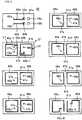
- the feed circuit board 20has a feed circuit 21 that contains a resonance circuit operating at a predetermined resonant frequency (and may contain an impedance matching circuit). As shown in Fig. 3 , the feed circuit 21 includes two coil-like inductance elements L1 and L2. The inductance elements L1 and L2 are electromagnetically coupled to end coupling portions 31 and 32 of the loop-like electrode 30.
- the loop-like electrode 30has a first section 30a, a second section 30b and a third section 30c.
- the loop-like electrode 30is electrically coupled (DC direct coupling) to the first electrode plate 50 at a coupling portion 33 located at the center of the third section 30c, and electromagnetically coupled to the second electrode plate 60 at the first section 30a.
- the wireless IC chip 10contains a clock circuit, a logic circuit, a memory circuit and so on, and stores necessary information therein.
- the back surface thereofis provided with a pair of input/output terminal electrodes and a pair of mounting terminal electrodes.
- the input/output terminal electrodes and the mounting terminal electrodesare electrically connected to feed terminal electrodes 42a and 42b (see Figs. 4 and 5 ) formed on the feed circuit board 20 and mounting electrodes 43a and 43b, respectively, via metallic bumps.
- the feed circuit board 20is attached to the loop-like electrode 30 by using a resin adhesive agent 56 in such a manner that the inductance elements L1 and L2 respectively face the end coupling portions 31 and 32 of the loop-like electrode 30.
- the inductance elements L1 and L2 contained in the feed circuit 21are magnetically coupled to each other with a reverse phase relationship to form a wider bandwidth, resonate with the frequency that the wireless IC chip 10 processes, and are electromagnetically coupled to the loop-like electrode 30.
- the feed circuit 21performs matching between the impedance (normally 50 ⁇ ) of the wireless IC chip 10 and the impedance (space impedance of 377 ⁇ ) of the first electrode plate 50 and the second electrode plate 60.
- the feed circuit 21transfers a transmission signal having a predetermined frequency transmitted from the wireless IC chip 10 to the first electrode plate 50 (and the second electrode plate 60), and selects a reception signal having a predetermined frequency from signals received by the first electrode plate 50 (and the second electrode plate 60) to supply the signal to the wireless IC chip 10.
- the wireless IC chip 10is operated by a signal received by the first electrode plate 50 (and the second electrode plate 60) and a reply signal from the wireless IC chip 10 is emitted to the outside from the first electrode plate 50 (and the second electrode plate 60).
- FIG. 6schematically shows the distribution of electromagnetic fields (magnetic field H and electric field E) generated by the loop-like electrode 30. Since the loop-like electrode 30 is disposed perpendicularly to the first electrode plate 50, a magnetic field H is generated parallel to the surface of the first electrode plate 50 and this induces an electric field E substantially perpendicular to the surface of the first electrode plate 50. A loop of this electric field E induces another loop of a magnetic field H, and due to this chain reaction, the distribution of electromagnetic fields widens.
- electromagnetic fieldselectromagnetic field H and electric field E
- the first electrode plate 50is mainly used for transmission and reception of a wireless signal
- the second electrode plate 60which is capacitively coupled to the first electrode plate 50, mainly functions as a shielding plate that shields against interruptions from other articles. Therefore, even when the present wireless IC device is attached to an article containing metal, water, salt or the like, the wireless IC device functions as a noncontact RFID system if the second electrode plate 60 is disposed so as to face the article side.
- the second electrode plate 60when the area of the second electrode plate 60 is larger than that of the first electrode plate 50, the second electrode plate 60 also functions as a radiation plate. In this case, the directivity is improved as the gain increases.
- the loop-like electrode 30can be formed to have a height of 10 mm or less, or even 1 mm or less, whereby reduction in size and thickness of the wireless IC device is not hindered. Note that, when the second electrode plate 60 is cylindrical, the directivity pattern of emission signals becomes generally circular, whereby it is possible to transmit and receive a signal from and to the second electrode plate 60, too.
- the feed circuit board 20has the following functions. Since the resonant frequency of a signal is set by the feed circuit 21 provided on the feed circuit board 20, the present wireless IC device operates on its own even when the wireless IC device is attached to various articles, and fluctuation in radiation characteristics is suppressed. Therefore, there is no need to change the design of the first electrode plate 50 and the second electrode plate 60 for individual articles. In addition, the frequency of a transmission signal emitted from the first electrode plate 50 (and the second electrode plate 60) and the frequency of a reception signal supplied to the wireless IC chip 10 substantially correspond to the resonant frequency of the feed circuit 21 in the feed circuit board 20. Therefore, stable frequency characteristics can be obtained.
- the feed circuit board 20is formed by laminating, pressure bonding and firing ceramic sheets 41a to 41h made of a dielectric material or a magnetic material.
- the top layer sheet 41ais provided with the feed terminal electrodes 42a and 42b, mounting electrodes 43a and 43b, and via hole conductors 44a, 44b, 45a and 45b.
- Each of the second to eighth layer sheets 41b to 41his provided with wiring electrodes 46a and 46b forming the inductance elements L1 and L2. As necessary, via hole conductors 47a, 47b, 48a and 48b are formed.
- the inductance element L1 in which the wiring electrodes 46a are spirally connected at the via hole conductors 47a, and the inductance element L2 in which the wiring electrodes 46b are spirally connected at the via hole conductors 47bare formed.
- a capacitanceis formed between the wiring electrodes 46a and 46b.
- An end section 46a-1 of the wiring electrode 46a on the sheet 41bis connected to the feed terminal electrode 42a via the via hole conductor 45a.
- An end section 46a-2 of the wiring electrode 46a on the sheet 41his connected to the feed terminal electrode 42b via the via hole conductors 48a and 45b.
- An end section 46b-1 of the wiring electrode 46b on the sheet 41bis connected to the feed terminal electrode 42b via the via hole conductor 44b.
- An end section 46b-2 of the wiring electrode 46b on the sheet 41his connected to the feed terminal electrode 42a via the via hole conductors 48b and 44a.
- the inductance elements L1 and L2are respectively wounded in opposite directions, whereby magnetic fields generated in the inductance elements L1 and L2 are cancelled out. Since the magnetic fields are cancelled out, it is necessary to increase the length of the wiring electrodes 46a and 46b to some extent in order to obtain a desired inductance value. This reduces the Q value and so the steepness of the resonance characteristic disappears, whereby a wider bandwidth is formed near the resonant frequency.
- the inductance elements L1 and L2are formed at different positions in the right and left when the feed circuit board 20 is viewed in plan view. In addition, the magnetic fields generated in the inductance elements L1 and L2 are opposite each other. Therefore, when the feed circuit 21 is coupled to the end coupling portions 31 and 32 of the loop-like electrode 30, currents flowing in opposite directions are excited in the coupling portions 31 and 32, and signals can be transmitted and received via the loop-like electrode 30. Note that, the inductance elements L1 and L2 may be electrically connected to the coupling portions 31 and 32.
- the feed circuit board 20may be a multilayer board made of ceramic or resin, or may be a board in which flexible sheets made of a dielectric material such as polyimide or liquid crystal polymer are laminated.
- the feed circuit 21is less likely to be influenced by the outside of the board, whereby fluctuation in radiation characteristics is suppressed.
- the feed circuit board 20may not be required, and the wireless IC chip 10 may be directly coupled to the coupling portions 31 and 32 of the loop-like electrode 30.
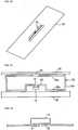
- the gain characteristic of the present wireless IC device obtained by using the loop-like electrode 30is shown in Fig. 8 .
- Data in Fig. 8is obtained by using the following specifications.
- the second electrode plate 60has dimensions of 30 ⁇ 30 mm and a thickness of 3 mm.
- the first electrode plate 50has a horizontal width C of 85 mm, a vertical width D of 45 mm, and a thickness of 100 ⁇ m.
- a clearance F between the third section 30c of the loop-like electrode 30 and the first electrode plate 50is 300 ⁇ m.
- a length G of the second section 30bis 2.2 mm.
- a clearance K between the first section 30a and the second electrode plate 60is 100 ⁇ m.
- a width M of the loop-like electrode 30is 200 ⁇ m.
- the wireless IC devicehas resonance points of Marker 1 and Marker 2.
- the Marker 1is a resonance point of the loop-like electrode 30, and the Marker 2 is a resonance point of the first electrode plate 50.
- the resonance point of the Marker 1varies with a dimension A of the coupling portion 33 and a spacing B with the first electrode plate 50. When the dimension A increases, the resonance point shifts toward the low frequency side. When the spacing B increases, the resonance point shifts toward the high frequency side.
- the resonance point of the Marker 2varies with the horizontal width C and the vertical width D of the first electrode plate 50. When the horizontal width C increases, the resonance point shifts toward the low frequency side. When the vertical width D increases, the resonance point shifts toward the high frequency side.
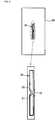
- a metallic thin plate 50(phosphoric bronze referred to as a hoop material can be preferably used or aluminum or the like may be used) having a thickness of 15 to 150 ⁇ m is patterned, as shown in Fig. 9 , by punching processing, etching processing or the like to form the loop-like electrode 30.
- the wireless IC chip 10 alone or the feed circuit board 20 having the wireless IC chip 10 mounted thereonis mounted (attached) on the end coupling portions 31 and 32 of the loop-like electrode 30.
- the loop-like electrode 30is bent so as to be perpendicular to or tilted with respect to the first electrode plate 50. Then, the loop-like electrode 30, together with the wireless IC chip 10 and the feed circuit board 20, is covered by the resin material 55. The loop-like electrode 30 may be inserted into a styrene foam plate. Then, the second electrode plate 60 is attached on the back side.
- a wireless IC devicewhich is a second embodiment
- the feed circuit board 20is omitted with respect to the first embodiment
- the wireless IC chip 10alone is electrically coupled to the end coupling portions 31 and 32 of the loop-like electrode 30.
- Other configurationsare the same as in the first embodiment.
- the function effect of the present second embodimentis basically the same as that of the first embodiment, and, in particular, the loop-like electrode 30 functions also as an inductance matching element.
- the wireless IC chip 10may be electromagnetically coupled to the loop-like electrode 30.
- the coupling portion 33 of the loop-like electrode 30is electromagnetically coupled to the first electrode plate 50 instead of directly connected thereto.
- Other configurationsare the same as in the first embodiment, and the function effect is also the same as that of the first embodiment.
- the third section 30c of the loop-like electrode 30is formed into a meandering shape.
- Other configurationsare the same as in the first embodiment, and the function effect is also the same as that of the first embodiment.
- the loop-like electrode 30can be formed in a compact size.
- the coupling section 33 of the loop-like electrode 30is electrically coupled to the first electrode plate 50 at two sites.
- Other configurationsare the same as in the first embodiment, and the function effect is also the same as that of the first embodiment.
- coupling forceis increased, and the coupling amount can be adjusted in accordance with the dimension A. As the dimension A increases, the resonance point of the Marker 1, shown in Fig. 8 , shifts toward the low frequency side.
- a part of a metallic article to which the wireless IC device is attachedis used as the second electrode plate 60.
- the metallic articleis a very wide concept such as, for example, an iron/steel plate, or a door, a body or a license plate of an automobile, or may be an electrode of a printed wiring board. That is, the "wireless IC device" of the present invention is not limited to a module formed of an electrode plate which is used as a radiation plate, and a wireless IC, but may contain an article itself.
- a meandering-shape impedance matching section 34is formed on the end coupling portions 31 and 32 of the loop-like electrode 30, and the first section 30a and the second section 30b function as a loop surface.
- Other configurationsare the same as in the first embodiment, and the function effect is also the same as that of the first embodiment.
- the wireless IC device and the method for manufacturing the same according to the present inventionare not limited to the foregoing embodiments. Various modifications are possible within the scope of the present invention.
- the present inventionis useful for a wireless IC device and a method for manufacturing the same, in particular, excellent in that the wireless IC device functions as a noncontact RFID system even when the wireless IC device is attached to an article containing metal, water, salt or the like, without hindering reduction in size and thickness.
Landscapes
- Details Of Aerials (AREA)
- Battery Mounting, Suspending (AREA)
Description
- The present invention relates to a wireless IC device, and more particularly, to a wireless IC device which is used in a noncontact RFID (Radio Frequency Identification) system, and a method for manufacturing the same.
- In recent years, wireless IC devices including a wireless IC chip which can electronically store information for article management and process a predetermined wireless signal, and an antenna which performs transmission and reception of the wireless signal between the wireless IC chip and a reader/writer have been attracting attention because of their various capabilities. A system using such a wireless IC device is generally called an RFID system, and can be used for individual authentication and transmission and reception of data in various occasions in accordance with a combination of a wireless IC device (in the form of card, tag, inlet, etc.) and a reader/writer which reads from and writes to the wireless IC device.
- Meanwhile, in such a noncontact RFID system, if an article to be attached to the wireless IC device contains metal, water, salt or the like, an eddy current is generated in the article, and therefore the antenna might not operate properly due to the eddy current. That is, when the antenna is attached to the article in a planar manner, an electromagnetic wave is absorbed due to the eddy current in a wireless IC device though depending on the frequency, especially one which operates in a high-frequency band, whereby the transmission and reception of information may fail or may be disabled.
- Therefore, for wireless IC devices which operate in an HF band, a method in which a magnetic member is disposed between the antenna and the article has been proposed (for example, see
Patent Documents - However, it is required that wireless IC devices be small and thin for various applications. When a magnetic member is disposed between the antenna and the article or when the antenna is disposed so as to be apart from the article, reduction in size and thickness cannot be fully achieved.
- [Patent Document 1] Japanese Unexamined Patent Application Publication No.
2004-304370 - [Patent Document 2] Japanese Unexamined Patent Application Publication No.
2005-340759 - [Patent Document 3] Japanese Unexamined Patent Application Publication No.
2006-13976 - [Patent Document 4] Japanese Unexamined Patent Application Publication No.
2007-172369 - [Patent Document 5] Japanese Unexamined Patent Application Publication No.
2007-172527 AU 2006261571 A1 - It is an object of the present invention to provide a wireless IC device which functions as a noncontact RFID system even when the wireless IC device is attached to an article containing metal, water, salt or the like, without hindering reduction in size and thickness, and a method for manufacturing the same.
- This object is achieved by a wireless IC device of
claim 1, and by a method ofclaim 5. - A wireless IC device, which is a first aspect of the present invention, is characterized by including,
a wireless IC that processes a predetermined wireless signal,
a loop-like electrode coupled to the wireless IC, and
a first electrode plate and a second electrode plate coupled to the loop-like electrode,
wherein the loop-like electrode is sandwiched between the first electrode plate and the second electrode plate,
wherein the loop-like electrode is disposed in such a manner that the loop surface thereof is perpendicular to or tilted with respect to the first electrode plate and the second electrode plate, and
wherein at least the first electrode plate out of the first electrode plate and the second electrode plate is used for transmission and reception of the wireless signal. - A method for manufacturing a wireless IC device, which is a second aspect of the present invention, the wireless IC device including,
a wireless IC that processes a predetermined wireless signal,
a loop-like electrode coupled to the wireless IC, and
a first electrode plate and a second electrode plate coupled to the loop-like electrode,
wherein the loop-like electrode is sandwiched between the first electrode plate and the second electrode plate,
wherein the loop-like electrode is disposed in such a manner that the loop surface thereof is perpendicular to or tilted with respect to the first electrode plate and the second electrode plate, and
wherein at least the first electrode plate out of the first electrode plate and the second electrode plate is used for transmission and reception of the wireless signal, is characterized by including,
a step of patterning the first electrode plate and the loop-like electrode on a sheet of a metallic plate, and
a step of bending the loop-like electrode so as to be perpendicular to or tilted with respect to the first electrode plate. - In the wireless IC device, since the loop-like electrode coupled to the wireless IC is sandwiched between the first electrode plate and the second electrode plate and is disposed in such a manner that the loop surface thereof is perpendicular to or tilted with respect to the first electrode plate and the second electrode plate, a magnetic field passing through the loop surface forms a magnetic field substantially parallel to the first electrode plate and the second electrode plate and a magnetic field electromagnetically coupled to the first electrode plate and the second electrode plate. In addition, the wireless IC is coupled to the first electrode plate and the second electrode plate via the loop-like electrode with small loss of energy. In addition, the first electrode plate is mainly used for transmission and reception of a wireless signal, and the second electrode plate mainly functions as a shielding plate that shields against interruptions from or to other articles and also functions as a radiation plate particularly when the area of the second electrode plate is larger than that of the first electrode plate. In this case, the directivity is improved as the gain increases. Therefore, even when the present wireless IC device is attached to an article containing metal, water, salt or the like, the wireless IC device functions as a noncontact RFID system if the second electrode plate is disposed so as to face the article side.
- According to the present invention, since the wireless IC is coupled to the first electrode plate and the second electrode plate via the loop-like electrode, and the loop-like electrode is sandwiched between the first electrode plate and the second electrode plate and is disposed in such a manner that the loop surface thereof is perpendicular to or tilted with respect to the first electrode plate and the second electrode plate, the wireless IC device maintains reduction in size and thickness, and functions as a noncontact RFID system even when the wireless IC device is attached to an article containing metal, water, salt or the like.
- [
Fig. 1] Fig. 1 illustrates a wireless IC device of a first embodiment.Fig. 1(A) is a front view andFig. 1(B) is a plan view. - [
Fig. 2] Fig. 2 is a front view illustrating a main section of the wireless IC device of the first embodiment. - [
Fig. 3] Fig. 3 is an equivalent circuit diagram of the wireless IC device of the first embodiment. - [
Fig. 4] Fig. 4 is a sectional view illustrating a feed circuit board of the wireless IC device of the first embodiment. - [
Fig. 5] Fig. 5 is an exploded view illustrating a layered structure of the feed circuit board of the wireless IC device of the first embodiment. - [
Fig. 6] Fig. 6 is an explanatory diagram illustrating an operation principle of a wireless IC device according to the present invention. - [
Fig. 7] Fig. 7 is another explanatory diagram illustrating an operation principle of the wireless IC device according to the present invention. - [
Fig. 8] Fig. 8 is a graph illustrating a gain characteristic of the wireless IC device of the first embodiment. - [
Fig. 9] Fig. 9 is a plan view illustrating a process of forming a loop-like electrode. - [
Fig. 10] Fig. 10 is a perspective view illustrating a process of forming the loop-like electrode. - [
Fig. 11] Fig. 11 is a front view illustrating a main section of a wireless IC device of a second embodiment. - [
Fig. 12] Fig. 12 is an explanatory diagram illustrating a main section of the wireless IC device of the second embodiment. - [
Fig. 13] Fig. 13 is a front view illustrating a main section of a wireless IC device of a third embodiment. - [
Fig. 14] Fig. 14 is a front view illustrating a main section of a wireless IC device of a fourth embodiment. - [
Fig. 15] Fig. 15 is a front view illustrating a main section of a wireless IC device of a fifth embodiment. - [
Fig. 16] Fig. 16 is a front view illustrating a wireless IC device of a sixth embodiment. - [
Fig. 17] Fig. 17 is a front view illustrating a main section of the wireless IC device of the sixth embodiment. - [
Fig. 18] Fig. 18 is a front view illustrating a main section of a wireless IC device of a seventh embodiment. - Embodiments of a wireless IC device and a method for manufacturing the same according to the present invention will be explained with reference to the accompanying drawings. Note that similar parts and sections are denoted by the same symbols, and repeated explanation will be omitted.
- As shown in
Fig. 1 , a wireless IC device, which is a first embodiment, is constituted by afeed circuit board 20 on which a wireless IC chip 10 (seeFig. 4 ) that processes transmission and reception signals having a predetermined frequency is mounted, a loop-like electrode 30 that is coupled to thewireless IC chip 10 via thefeed circuit board 20, and afirst electrode plate 50 and asecond electrode plate 60 that are coupled to the loop-like electrode 30. - As shown in
Fig. 2 , the loop-like electrode 30 is sandwiched between thefirst electrode plate 50 and thesecond electrode plate 60 and is disposed in such a manner that the loop surface thereof is perpendicular to (or tilted with respect to) thefirst electrode plate 50 and thesecond electrode plate 60. Thefirst electrode plate 50 and thesecond electrode plate 60 may be formed of either a magnetic material or a non-magnetic material as long as the material is a metal such as iron or aluminum. In addition to the loop-like electrode 30 and thefeed circuit board 20, aresin material 55 is filled between thefirst electrode plate 50 and thesecond electrode plate 60. InFig. 1 , thesecond electrode plate 60 has an area larger than that of thefirst electrode plate 50 but may have the same area as that of thefirst electrode plate 50. - The
feed circuit board 20 has afeed circuit 21 that contains a resonance circuit operating at a predetermined resonant frequency (and may contain an impedance matching circuit). As shown inFig. 3 , thefeed circuit 21 includes two coil-like inductance elements L1 and L2. The inductance elements L1 and L2 are electromagnetically coupled to endcoupling portions like electrode 30. The loop-like electrode 30 has a first section 30a, asecond section 30b and athird section 30c. The loop-like electrode 30 is electrically coupled (DC direct coupling) to thefirst electrode plate 50 at acoupling portion 33 located at the center of thethird section 30c, and electromagnetically coupled to thesecond electrode plate 60 at the first section 30a. - The
wireless IC chip 10 contains a clock circuit, a logic circuit, a memory circuit and so on, and stores necessary information therein. The back surface thereof is provided with a pair of input/output terminal electrodes and a pair of mounting terminal electrodes. The input/output terminal electrodes and the mounting terminal electrodes are electrically connected to feedterminal electrodes Figs. 4 and5 ) formed on thefeed circuit board 20 and mountingelectrodes 43a and 43b, respectively, via metallic bumps. Thefeed circuit board 20 is attached to the loop-like electrode 30 by using a resinadhesive agent 56 in such a manner that the inductance elements L1 and L2 respectively face theend coupling portions like electrode 30. - The inductance elements L1 and L2 contained in the
feed circuit 21 are magnetically coupled to each other with a reverse phase relationship to form a wider bandwidth, resonate with the frequency that thewireless IC chip 10 processes, and are electromagnetically coupled to the loop-like electrode 30. In addition, thefeed circuit 21 performs matching between the impedance (normally 50 Ω) of thewireless IC chip 10 and the impedance (space impedance of 377 Ω) of thefirst electrode plate 50 and thesecond electrode plate 60. - Therefore, the
feed circuit 21 transfers a transmission signal having a predetermined frequency transmitted from thewireless IC chip 10 to the first electrode plate 50 (and the second electrode plate 60), and selects a reception signal having a predetermined frequency from signals received by the first electrode plate 50 (and the second electrode plate 60) to supply the signal to thewireless IC chip 10. Thus, in this wireless IC device, thewireless IC chip 10 is operated by a signal received by the first electrode plate 50 (and the second electrode plate 60) and a reply signal from thewireless IC chip 10 is emitted to the outside from the first electrode plate 50 (and the second electrode plate 60). - Here, an operation principle of the present wireless IC device is explained with reference to
Figs. 6 and 7. Fig. 6 schematically shows the distribution of electromagnetic fields (magnetic field H and electric field E) generated by the loop-like electrode 30. Since the loop-like electrode 30 is disposed perpendicularly to thefirst electrode plate 50, a magnetic field H is generated parallel to the surface of thefirst electrode plate 50 and this induces an electric field E substantially perpendicular to the surface of thefirst electrode plate 50. A loop of this electric field E induces another loop of a magnetic field H, and due to this chain reaction, the distribution of electromagnetic fields widens. - In addition, as shown in
Fig. 7 , due to a high-frequency signal (magnetic field H1) from the reader/writer, an eddy current J is generated all over the surface of thefirst electrode plate 50, and this eddy current J causes a magnetic field H2 to be generated in a direction perpendicular to the surface of thefirst electrode plate 50. Then, the loop-like electrode 30 is coupled to the magnetic field H2. - Accordingly, the
first electrode plate 50 is mainly used for transmission and reception of a wireless signal, and thesecond electrode plate 60, which is capacitively coupled to thefirst electrode plate 50, mainly functions as a shielding plate that shields against interruptions from other articles. Therefore, even when the present wireless IC device is attached to an article containing metal, water, salt or the like, the wireless IC device functions as a noncontact RFID system if thesecond electrode plate 60 is disposed so as to face the article side. In addition, when the area of thesecond electrode plate 60 is larger than that of thefirst electrode plate 50, thesecond electrode plate 60 also functions as a radiation plate. In this case, the directivity is improved as the gain increases. The loop-like electrode 30 can be formed to have a height of 10 mm or less, or even 1 mm or less, whereby reduction in size and thickness of the wireless IC device is not hindered. Note that, when thesecond electrode plate 60 is cylindrical, the directivity pattern of emission signals becomes generally circular, whereby it is possible to transmit and receive a signal from and to thesecond electrode plate 60, too. - In the present first embodiment, the
feed circuit board 20 has the following functions. Since the resonant frequency of a signal is set by thefeed circuit 21 provided on thefeed circuit board 20, the present wireless IC device operates on its own even when the wireless IC device is attached to various articles, and fluctuation in radiation characteristics is suppressed. Therefore, there is no need to change the design of thefirst electrode plate 50 and thesecond electrode plate 60 for individual articles. In addition, the frequency of a transmission signal emitted from the first electrode plate 50 (and the second electrode plate 60) and the frequency of a reception signal supplied to thewireless IC chip 10 substantially correspond to the resonant frequency of thefeed circuit 21 in thefeed circuit board 20. Therefore, stable frequency characteristics can be obtained. - Here, the configuration of the
feed circuit board 20 is explained with reference toFig. 5 . Thefeed circuit board 20 is formed by laminating, pressure bonding and firingceramic sheets 41a to 41h made of a dielectric material or a magnetic material. Thetop layer sheet 41a is provided with thefeed terminal electrodes electrodes 43a and 43b, and viahole conductors eighth layer sheets 41b to 41h is provided withwiring electrodes hole conductors - By laminating the
above sheets 41a to 41h, the inductance element L1 in which thewiring electrodes 46a are spirally connected at the via hole conductors 47a, and the inductance element L2 in which thewiring electrodes 46b are spirally connected at the viahole conductors 47b are formed. In addition, a capacitance is formed between thewiring electrodes - An
end section 46a-1 of thewiring electrode 46a on thesheet 41b is connected to thefeed terminal electrode 42a via the via hole conductor 45a. Anend section 46a-2 of thewiring electrode 46a on thesheet 41h is connected to thefeed terminal electrode 42b via the viahole conductors 48a and 45b. Anend section 46b-1 of thewiring electrode 46b on thesheet 41b is connected to thefeed terminal electrode 42b via the viahole conductor 44b. Anend section 46b-2 of thewiring electrode 46b on thesheet 41h is connected to thefeed terminal electrode 42a via the viahole conductors - In the
feed circuit 21 described above, the inductance elements L1 and L2 are respectively wounded in opposite directions, whereby magnetic fields generated in the inductance elements L1 and L2 are cancelled out. Since the magnetic fields are cancelled out, it is necessary to increase the length of thewiring electrodes - The inductance elements L1 and L2 are formed at different positions in the right and left when the
feed circuit board 20 is viewed in plan view. In addition, the magnetic fields generated in the inductance elements L1 and L2 are opposite each other. Therefore, when thefeed circuit 21 is coupled to theend coupling portions like electrode 30, currents flowing in opposite directions are excited in thecoupling portions like electrode 30. Note that, the inductance elements L1 and L2 may be electrically connected to thecoupling portions - Note that, the
feed circuit board 20 may be a multilayer board made of ceramic or resin, or may be a board in which flexible sheets made of a dielectric material such as polyimide or liquid crystal polymer are laminated. In particular, when the inductance elements L1 and L2 are embedded in thefeed circuit board 20, thefeed circuit 21 is less likely to be influenced by the outside of the board, whereby fluctuation in radiation characteristics is suppressed. - Note that, in the wireless IC device which is the present first embodiment, the
feed circuit board 20 may not be required, and thewireless IC chip 10 may be directly coupled to thecoupling portions like electrode 30. - The gain characteristic of the present wireless IC device obtained by using the loop-
like electrode 30 is shown inFig. 8 . Data inFig. 8 is obtained by using the following specifications. Thesecond electrode plate 60 has dimensions of 30 × 30 mm and a thickness of 3 mm. Thefirst electrode plate 50 has a horizontal width C of 85 mm, a vertical width D of 45 mm, and a thickness of 100 µm. A clearance F between thethird section 30c of the loop-like electrode 30 and thefirst electrode plate 50 is 300 µm. A length G of thesecond section 30b is 2.2 mm. A clearance K between the first section 30a and thesecond electrode plate 60 is 100 µm. A width M of the loop-like electrode 30 is 200 µm. - As is apparent from
Fig. 8 , the wireless IC device has resonance points ofMarker 1 andMarker 2. TheMarker 1 is a resonance point of the loop-like electrode 30, and theMarker 2 is a resonance point of thefirst electrode plate 50. The resonance point of theMarker 1 varies with a dimension A of thecoupling portion 33 and a spacing B with thefirst electrode plate 50. When the dimension A increases, the resonance point shifts toward the low frequency side. When the spacing B increases, the resonance point shifts toward the high frequency side. The resonance point of theMarker 2 varies with the horizontal width C and the vertical width D of thefirst electrode plate 50. When the horizontal width C increases, the resonance point shifts toward the low frequency side. When the vertical width D increases, the resonance point shifts toward the high frequency side. - Next, an example of a method for manufacturing the wireless IC device is explained. First, a metallic thin plate 50 (phosphoric bronze referred to as a hoop material can be preferably used or aluminum or the like may be used) having a thickness of 15 to 150 µm is patterned, as shown in
Fig. 9 , by punching processing, etching processing or the like to form the loop-like electrode 30. Next, thewireless IC chip 10 alone or thefeed circuit board 20 having thewireless IC chip 10 mounted thereon is mounted (attached) on theend coupling portions like electrode 30. - Next, as shown in
Fig. 10 , the loop-like electrode 30 is bent so as to be perpendicular to or tilted with respect to thefirst electrode plate 50. Then, the loop-like electrode 30, together with thewireless IC chip 10 and thefeed circuit board 20, is covered by theresin material 55. The loop-like electrode 30 may be inserted into a styrene foam plate. Then, thesecond electrode plate 60 is attached on the back side. - As shown in
Figs. 11 and 12 , in a wireless IC device which is a second embodiment, thefeed circuit board 20 is omitted with respect to the first embodiment, and thewireless IC chip 10 alone is electrically coupled to theend coupling portions like electrode 30. Other configurations are the same as in the first embodiment. The function effect of the present second embodiment is basically the same as that of the first embodiment, and, in particular, the loop-like electrode 30 functions also as an inductance matching element. Note that, thewireless IC chip 10 may be electromagnetically coupled to the loop-like electrode 30. - As shown in
Fig. 13 , in a wireless IC device which is a third embodiment, thecoupling portion 33 of the loop-like electrode 30 is electromagnetically coupled to thefirst electrode plate 50 instead of directly connected thereto. Other configurations are the same as in the first embodiment, and the function effect is also the same as that of the first embodiment. - As shown in
Fig. 14 , in a wireless IC device which is a fourth embodiment, thethird section 30c of the loop-like electrode 30 is formed into a meandering shape. Other configurations are the same as in the first embodiment, and the function effect is also the same as that of the first embodiment. In particular, the loop-like electrode 30 can be formed in a compact size. - As shown in
Fig. 15 , in a wireless IC device which is a fifth embodiment, thecoupling section 33 of the loop-like electrode 30 is electrically coupled to thefirst electrode plate 50 at two sites. Other configurations are the same as in the first embodiment, and the function effect is also the same as that of the first embodiment. In particular, coupling force is increased, and the coupling amount can be adjusted in accordance with the dimension A. As the dimension A increases, the resonance point of theMarker 1, shown inFig. 8 , shifts toward the low frequency side. - As shown in
Figs. 16 and17 , in a wireless IC device which is a sixth embodiment, a part of a metallic article to which the wireless IC device is attached is used as thesecond electrode plate 60. Other configurations are the same as in the first embodiment, and the function effect is also the same as that of the first embodiment. In this case, the metallic article is a very wide concept such as, for example, an iron/steel plate, or a door, a body or a license plate of an automobile, or may be an electrode of a printed wiring board. That is, the "wireless IC device" of the present invention is not limited to a module formed of an electrode plate which is used as a radiation plate, and a wireless IC, but may contain an article itself. - As shown in
Fig. 18 , in a wireless IC device which is a seventh embodiment, a meandering-shapeimpedance matching section 34 is formed on theend coupling portions like electrode 30, and the first section 30a and thesecond section 30b function as a loop surface. Other configurations are the same as in the first embodiment, and the function effect is also the same as that of the first embodiment. - Note that, the wireless IC device and the method for manufacturing the same according to the present invention are not limited to the foregoing embodiments. Various modifications are possible within the scope of the present invention.
- Accordingly, the present invention is useful for a wireless IC device and a method for manufacturing the same, in particular, excellent in that the wireless IC device functions as a noncontact RFID system even when the wireless IC device is attached to an article containing metal, water, salt or the like, without hindering reduction in size and thickness.
- 10
- Wireless IC chip
- 20
- Feed circuit board
- 21
- Feed circuit
- 30
- Loop-like electrode
- 50
- First electrode plate
- 60
- Second electrode plate
- L1 and L2
- Inductance elements
Claims (5)
- A wireless IC device, comprising:a wireless IC (10) that processes a predetermined wireless signal;a loop-like electrode (30) coupled to the wireless IC (10); anda first electrode plate (50) and a second electrode plate (60) coupled to the loop-like electrode (30),wherein the loop-like electrode (30) is sandwiched between the first electrode plate (50) and the second electrode plate (60),wherein the loop-like electrode (30) is disposed in such a manner that at least a part of a loop surface thereof is perpendicular to or tilted with respect to the first electrode plate (50) and the second electrode plate (60),wherein at least the first electrode plate (50) out of the first electrode plate (50) and the second electrode plate (60) is used for transmission and reception of the wireless signal,wherein a feed circuit board (20) having a feed circuit (21) containing a resonance circuit that operates at a predetermined resonant frequency is provided between the wireless IC (10) and the loop-like electrode (30).
- The wireless IC device according to claim 1,characterized in that the loop-like electrode (30) and the first electrode plate (50) are electrically coupled to each other, and the loop-like electrode (30) and the second electrode plate (60) are electromagnetically coupled to each other.
- The wireless IC device according to claim 1 or 2,characterized in that the feed circuit (21) contains inductance elements (L1, L2), and the feed circuit board (20) and the loop-like electrode (30) are electromagnetically coupled to each other via the inductance elements (L1, L2).
- The wireless IC device according to any one of claims 1 to 3,characterized in that a part of a metallic article is used as the second electrode plate (60).
- A method for manufacturing a wireless IC device of one of claims 1 to 4, the method comprising:a step of patterning the first electrode plate (50) and the loop-like electrode (30) on a sheet of a metallic plate; anda step of bending the loop-like electrode (30) so as to be perpendicular to or tilted with respect to the first electrode plate (50).
Applications Claiming Priority (2)
| Application Number | Priority Date | Filing Date | Title |
|---|---|---|---|
| JP2008211200 | 2008-08-19 | ||
| PCT/JP2009/062801WO2010021217A1 (en) | 2008-08-19 | 2009-07-15 | Wireless ic device and method for manufacturing same |
Publications (3)
| Publication Number | Publication Date |
|---|---|
| EP2320519A1 EP2320519A1 (en) | 2011-05-11 |
| EP2320519A4 EP2320519A4 (en) | 2012-09-05 |
| EP2320519B1true EP2320519B1 (en) | 2017-04-12 |
Family
ID=41707095
Family Applications (1)
| Application Number | Title | Priority Date | Filing Date |
|---|---|---|---|
| EP09808153.2ANot-in-forceEP2320519B1 (en) | 2008-08-19 | 2009-07-15 | Wireless ic device and method for manufacturing same |
Country Status (5)
| Country | Link |
|---|---|
| US (1) | US8870077B2 (en) |
| EP (1) | EP2320519B1 (en) |
| JP (1) | JP5434920B2 (en) |
| CN (1) | CN102124605A (en) |
| WO (1) | WO2010021217A1 (en) |
Families Citing this family (13)
| Publication number | Priority date | Publication date | Assignee | Title |
|---|---|---|---|---|
| JP2913049B2 (en) | 1989-06-30 | 1999-06-28 | 京セラ株式会社 | Piezoelectric porcelain composition |
| JP2789374B2 (en) | 1990-04-28 | 1998-08-20 | 京セラ株式会社 | Piezoelectric ceramic composition |
| JP2964265B2 (en) | 1990-07-31 | 1999-10-18 | 京セラ株式会社 | Piezoelectric porcelain composition |
| JP2957002B2 (en) | 1990-10-31 | 1999-10-04 | 京セラ株式会社 | Piezoelectric porcelain composition |
| JP4605318B2 (en) | 2008-11-17 | 2011-01-05 | 株式会社村田製作所 | Antenna and wireless IC device |
| BRPI1002245A2 (en)* | 2010-07-23 | 2012-06-05 | Albuquerque Lambert Jorge De | self-protected antenna with application to (but not limited to) RFID electronic documents intrinsically protected against clandestine activation |
| WO2012051233A1 (en)* | 2010-10-12 | 2012-04-19 | Molex Incorporated | Low impedance slot fed antenna |
| US20120293109A1 (en)* | 2011-05-19 | 2012-11-22 | Yariv Glazer | Method and System for Efficiently Exploiting Renewable Electrical Energy Sources |
| WO2013008375A1 (en)* | 2011-07-12 | 2013-01-17 | 株式会社村田製作所 | Communication body for transmitting signals, and coupler |
| TWI488367B (en)* | 2011-11-15 | 2015-06-11 | Ind Tech Res Inst | Rfid tag antenna |
| CN104471788B (en)* | 2012-07-11 | 2017-05-10 | 株式会社村田制作所 | Communication apparatus |
| JP6079932B2 (en)* | 2014-04-28 | 2017-02-15 | 株式会社村田製作所 | Wireless IC device, clip-shaped RFID tag, and article with RFID tag |
| CN109075449A (en)* | 2016-04-14 | 2018-12-21 | Nok株式会社 | The manufacturing method of IC label and IC label |
Citations (1)
| Publication number | Priority date | Publication date | Assignee | Title |
|---|---|---|---|---|
| US20070164414A1 (en)* | 2006-01-19 | 2007-07-19 | Murata Manufacturing Co., Ltd. | Wireless ic device and component for wireless ic device |
Family Cites Families (484)
| Publication number | Priority date | Publication date | Assignee | Title |
|---|---|---|---|---|
| US3364564A (en) | 1965-06-28 | 1968-01-23 | Gregory Ind Inc | Method of producing welding studs dischargeable in end-to-end relationship |
| JPS5754964B2 (en) | 1974-05-08 | 1982-11-20 | ||
| JPS6193701A (en) | 1984-10-13 | 1986-05-12 | Toyota Motor Corp | Automotive antenna device |
| JPS61284102A (en) | 1985-06-11 | 1986-12-15 | Oki Electric Ind Co Ltd | Antenna for portable radio equipment |
| JPS62127140U (en) | 1986-02-03 | 1987-08-12 | ||
| JPH01212035A (en) | 1987-08-13 | 1989-08-25 | Secom Co Ltd | Electromagnetic field diversity reception method |
| ZA89872B (en) | 1988-02-04 | 1990-10-31 | Uniscan Ltd | Concentrator |
| JPH0744114B2 (en) | 1988-12-16 | 1995-05-15 | 株式会社村田製作所 | Multilayer chip coil |
| JPH02164105A (en) | 1988-12-19 | 1990-06-25 | Mitsubishi Electric Corp | spiral antenna |
| US5253969A (en) | 1989-03-10 | 1993-10-19 | Sms Schloemann-Siemag Aktiengesellschaft | Feeding system for strip material, particularly in treatment plants for metal strips |
| JPH03171385A (en) | 1989-11-30 | 1991-07-24 | Sony Corp | Information card |
| JP2662742B2 (en) | 1990-03-13 | 1997-10-15 | 株式会社村田製作所 | Bandpass filter |
| JP2763664B2 (en) | 1990-07-25 | 1998-06-11 | 日本碍子株式会社 | Wiring board for distributed constant circuit |
| JPH04150011A (en) | 1990-10-12 | 1992-05-22 | Tdk Corp | Composite electronic component |
| JPH04167500A (en) | 1990-10-30 | 1992-06-15 | Omron Corp | Printed-circuit board management system |
| JP2539367Y2 (en) | 1991-01-30 | 1997-06-25 | 株式会社村田製作所 | Multilayer electronic components |
| NL9100176A (en) | 1991-02-01 | 1992-03-02 | Nedap Nv | Antenna configuration for contactless identification label - forms part of tuned circuit of ID or credit card interrogated via inductive coupling |
| JP2558330Y2 (en) | 1991-02-06 | 1997-12-24 | オムロン株式会社 | Electromagnetic coupling type electronic equipment |
| NL9100347A (en) | 1991-02-26 | 1992-03-02 | Nedap Nv | Integrated transformer circuit for ID or credit card - is interrogated via contactless inductive coupling using capacitor to form tuned circuit |
| JPH04321190A (en) | 1991-04-22 | 1992-11-11 | Mitsubishi Electric Corp | Antenna circuit and its production for non-contact type portable storage |
| JPH0745933Y2 (en) | 1991-06-07 | 1995-10-18 | 太陽誘電株式会社 | Multilayer ceramic inductance element |
| DE69215283T2 (en) | 1991-07-08 | 1997-03-20 | Nippon Telegraph & Telephone | Extendable antenna system |
| JP2839782B2 (en) | 1992-02-14 | 1998-12-16 | 三菱電機株式会社 | Printed slot antenna |
| JPH05327331A (en) | 1992-05-15 | 1993-12-10 | Matsushita Electric Works Ltd | Printed antenna |
| JP3186235B2 (en) | 1992-07-30 | 2001-07-11 | 株式会社村田製作所 | Resonator antenna |
| JPH0677729A (en) | 1992-08-25 | 1994-03-18 | Mitsubishi Electric Corp | Antenna integrated microwave circuit |
| JP2592328Y2 (en) | 1992-09-09 | 1999-03-17 | 神鋼電機株式会社 | Antenna device |
| JPH06177635A (en) | 1992-12-07 | 1994-06-24 | Mitsubishi Electric Corp | Cross dipole antenna system |
| JPH06260949A (en) | 1993-03-03 | 1994-09-16 | Seiko Instr Inc | Radio equipment |
| JPH07183836A (en) | 1993-12-22 | 1995-07-21 | San'eisha Mfg Co Ltd | Coupling filter device for distribution line carrier communication |
| US5491483A (en) | 1994-01-05 | 1996-02-13 | Texas Instruments Incorporated | Single loop transponder system and method |
| US6096431A (en) | 1994-07-25 | 2000-08-01 | Toppan Printing Co., Ltd. | Biodegradable cards |
| JP3427527B2 (en) | 1994-12-26 | 2003-07-22 | 凸版印刷株式会社 | Biodegradable laminate and biodegradable card |
| JP2999374B2 (en) | 1994-08-10 | 2000-01-17 | 太陽誘電株式会社 | Multilayer chip inductor |
| JP3141692B2 (en) | 1994-08-11 | 2001-03-05 | 松下電器産業株式会社 | Millimeter wave detector |
| DE4431754C1 (en) | 1994-09-06 | 1995-11-23 | Siemens Ag | Carrier element for ic module of chip card |
| US5528222A (en) | 1994-09-09 | 1996-06-18 | International Business Machines Corporation | Radio frequency circuit and memory in thin flexible package |
| JPH0887580A (en) | 1994-09-14 | 1996-04-02 | Omron Corp | Data carrier and ball game |
| JP3064840B2 (en) | 1994-12-22 | 2000-07-12 | ソニー株式会社 | IC card |
| JP2837829B2 (en) | 1995-03-31 | 1998-12-16 | 松下電器産業株式会社 | Inspection method for semiconductor device |
| JPH08279027A (en) | 1995-04-04 | 1996-10-22 | Toshiba Corp | Wireless communication card |
| US5955723A (en) | 1995-05-03 | 1999-09-21 | Siemens Aktiengesellschaft | Contactless chip card |
| JPH08307126A (en) | 1995-05-09 | 1996-11-22 | Kyocera Corp | Antenna storage structure |
| JP3637982B2 (en) | 1995-06-27 | 2005-04-13 | 株式会社荏原電産 | Inverter-driven pump control system |
| US5629241A (en) | 1995-07-07 | 1997-05-13 | Hughes Aircraft Company | Microwave/millimeter wave circuit structure with discrete flip-chip mounted elements, and method of fabricating the same |
| JP3150575B2 (en) | 1995-07-18 | 2001-03-26 | 沖電気工業株式会社 | Tag device and manufacturing method thereof |
| GB2305075A (en) | 1995-09-05 | 1997-03-26 | Ibm | Radio Frequency Tag for Electronic Apparatus |
| DE19534229A1 (en) | 1995-09-15 | 1997-03-20 | Licentia Gmbh | Transponder arrangement |
| JPH0993029A (en) | 1995-09-21 | 1997-04-04 | Matsushita Electric Ind Co Ltd | Antenna device |
| JP3882218B2 (en) | 1996-03-04 | 2007-02-14 | ソニー株式会社 | optical disk |
| JP3471160B2 (en) | 1996-03-18 | 2003-11-25 | 株式会社東芝 | Monolithic antenna |
| JPH09270623A (en) | 1996-03-29 | 1997-10-14 | Murata Mfg Co Ltd | Antenna system |
| JPH09284038A (en) | 1996-04-17 | 1997-10-31 | Nhk Spring Co Ltd | Antenna equipment of non-contact data carrier |
| JP3427663B2 (en) | 1996-06-18 | 2003-07-22 | 凸版印刷株式会社 | Non-contact IC card |
| AUPO055296A0 (en) | 1996-06-19 | 1996-07-11 | Integrated Silicon Design Pty Ltd | Enhanced range transponder system |
| US6104311A (en) | 1996-08-26 | 2000-08-15 | Addison Technologies | Information storage and identification tag |
| AU4705097A (en) | 1996-10-09 | 1998-05-05 | Evc Rigid Film Gmbh | Method and connection arrangement for producing a smart card |
| JPH10171954A (en) | 1996-12-05 | 1998-06-26 | Hitachi Maxell Ltd | Non-contact IC card |
| JP3279205B2 (en) | 1996-12-10 | 2002-04-30 | 株式会社村田製作所 | Surface mount antenna and communication equipment |
| JPH10193849A (en) | 1996-12-27 | 1998-07-28 | Rohm Co Ltd | Circuit chip-mounted card and circuit chip module |
| JPH10193851A (en) | 1997-01-08 | 1998-07-28 | Denso Corp | Non-contact card |
| DE19703029A1 (en) | 1997-01-28 | 1998-07-30 | Amatech Gmbh & Co Kg | Transmission module for a transponder device and transponder device and method for operating a transponder device |
| JPH10242742A (en) | 1997-02-26 | 1998-09-11 | Harada Ind Co Ltd | Transmitting and receiving antenna |
| US6181287B1 (en) | 1997-03-10 | 2001-01-30 | Precision Dynamics Corporation | Reactively coupled elements in circuits on flexible substrates |
| JPH10293828A (en) | 1997-04-18 | 1998-11-04 | Omron Corp | Data carrier, coil module, reader / writer, and clothing data acquisition method |
| JP3900593B2 (en) | 1997-05-27 | 2007-04-04 | 凸版印刷株式会社 | IC card and IC module |
| JPH11346114A (en) | 1997-06-11 | 1999-12-14 | Matsushita Electric Ind Co Ltd | Antenna device |
| JPH1125244A (en) | 1997-06-27 | 1999-01-29 | Toshiba Chem Corp | Non-contact data carrier package |
| JP3621560B2 (en) | 1997-07-24 | 2005-02-16 | 三菱電機株式会社 | Electromagnetic induction data carrier system |
| JPH1175329A (en) | 1997-08-29 | 1999-03-16 | Hitachi Ltd | Non-contact IC card system |
| JPH1185937A (en) | 1997-09-02 | 1999-03-30 | Nippon Lsi Card Kk | Non-contact lsi card and method for inspecting the same |
| JPH1188241A (en) | 1997-09-04 | 1999-03-30 | Nippon Steel Corp | Data carrier system |
| JPH11103209A (en) | 1997-09-26 | 1999-04-13 | Fujitsu Ten Ltd | Radio wave reception equipment |
| JP3853930B2 (en) | 1997-09-26 | 2006-12-06 | 株式会社マースエンジニアリング | Non-contact data carrier package and manufacturing method thereof |
| JP3800765B2 (en) | 1997-11-14 | 2006-07-26 | 凸版印刷株式会社 | Compound IC card |
| JPH11149536A (en) | 1997-11-14 | 1999-06-02 | Toppan Printing Co Ltd | Composite IC card |
| CN1179295C (en) | 1997-11-14 | 2004-12-08 | 凸版印刷株式会社 | Composite IC module and composite IC card |
| JP3800766B2 (en) | 1997-11-14 | 2006-07-26 | 凸版印刷株式会社 | Compound IC module and compound IC card |
| JPH11175678A (en) | 1997-12-09 | 1999-07-02 | Toppan Printing Co Ltd | IC module and IC card mounting the module |
| JPH11220319A (en) | 1998-01-30 | 1999-08-10 | Sharp Corp | Antenna device |
| JPH11219420A (en) | 1998-02-03 | 1999-08-10 | Tokin Corp | Ic card module, ic card and their manufacture |
| JP2001084463A (en) | 1999-09-14 | 2001-03-30 | Miyake:Kk | Resonance circuit |
| JPH11261325A (en) | 1998-03-10 | 1999-09-24 | Shiro Sugimura | Coil element and manufacturing method thereof |
| JP4260917B2 (en) | 1998-03-31 | 2009-04-30 | 株式会社東芝 | Loop antenna |
| EP0987789A4 (en) | 1998-03-31 | 2004-09-22 | Matsushita Electric Industrial Co Ltd | ANTENNA AND DIGITAL TELEVISION |
| US5936150A (en) | 1998-04-13 | 1999-08-10 | Rockwell Science Center, Llc | Thin film resonant chemical sensor with resonant acoustic isolator |
| JP2002505645A (en) | 1998-04-14 | 2002-02-19 | リバティ・カートン・カンパニー−テキサス | Container for compressors and other goods |
| JP4030651B2 (en) | 1998-05-12 | 2008-01-09 | 三菱電機株式会社 | Mobile phone |
| JPH11328352A (en) | 1998-05-19 | 1999-11-30 | Tokin Corp | Connection structure between antenna and ic chip, and ic card |
| US6018299A (en) | 1998-06-09 | 2000-01-25 | Motorola, Inc. | Radio frequency identification tag having a printed antenna and method |
| US6107920A (en) | 1998-06-09 | 2000-08-22 | Motorola, Inc. | Radio frequency identification tag having an article integrated antenna |
| JP2000021639A (en) | 1998-07-02 | 2000-01-21 | Sharp Corp | Inductor, resonance circuit, matching circuit, antenna circuit and oscillation circuit using the same |
| JP2000022421A (en) | 1998-07-03 | 2000-01-21 | Murata Mfg Co Ltd | Chip antenna and radio device mounted with it |
| JP2000021128A (en) | 1998-07-03 | 2000-01-21 | Nippon Steel Corp | Disk-shaped storage medium and its storage case |
| AUPP473898A0 (en) | 1998-07-20 | 1998-08-13 | Integrated Silicon Design Pty Ltd | Metal screened electronic labelling system |
| JP2000311226A (en) | 1998-07-28 | 2000-11-07 | Toshiba Corp | Wireless IC card, manufacturing method thereof, and wireless IC card read / write system |
| EP0977145A3 (en) | 1998-07-28 | 2002-11-06 | Kabushiki Kaisha Toshiba | Radio IC card |
| JP2000059260A (en) | 1998-08-04 | 2000-02-25 | Sony Corp | Storage device |
| JP2002522999A (en) | 1998-08-14 | 2002-07-23 | スリーエム イノベイティブ プロパティズ カンパニー | Applications to radio frequency identification systems |
| KR100699755B1 (en) | 1998-08-14 | 2007-03-27 | 쓰리엠 이노베이티브 프로퍼티즈 캄파니 | Radio Frequency Identification System Applications |
| JP4411670B2 (en) | 1998-09-08 | 2010-02-10 | 凸版印刷株式会社 | Non-contact IC card manufacturing method |
| JP4508301B2 (en) | 1998-09-16 | 2010-07-21 | 大日本印刷株式会社 | Non-contact IC card |
| JP3632466B2 (en) | 1998-10-23 | 2005-03-23 | 凸版印刷株式会社 | Inspection device and inspection method for non-contact IC card |
| JP2000137779A (en) | 1998-10-30 | 2000-05-16 | Hitachi Maxell Ltd | Non-contact information medium and its manufacturing method |
| US6837438B1 (en) | 1998-10-30 | 2005-01-04 | Hitachi Maxell, Ltd. | Non-contact information medium and communication system utilizing the same |
| JP3924962B2 (en) | 1998-10-30 | 2007-06-06 | 株式会社デンソー | ID tag for dishes |
| JP2000137785A (en) | 1998-10-30 | 2000-05-16 | Sony Corp | Manufacture of noncontact type ic card and noncontact type ic card |
| JP2000148948A (en) | 1998-11-05 | 2000-05-30 | Sony Corp | Non-contact ic label and its manufacture |
| JP2000172812A (en) | 1998-12-08 | 2000-06-23 | Hitachi Maxell Ltd | Noncontact information medium |
| FR2787640B1 (en) | 1998-12-22 | 2003-02-14 | Gemplus Card Int | ARRANGEMENT OF AN ANTENNA IN A METALLIC ENVIRONMENT |
| JP3088404B2 (en) | 1999-01-14 | 2000-09-18 | 埼玉日本電気株式会社 | Mobile radio terminal and built-in antenna |
| JP2000222540A (en) | 1999-02-03 | 2000-08-11 | Hitachi Maxell Ltd | Non-contact type semiconductor tag |
| JP2000228602A (en) | 1999-02-08 | 2000-08-15 | Alps Electric Co Ltd | Resonance line |
| JP2000243797A (en) | 1999-02-18 | 2000-09-08 | Sanken Electric Co Ltd | Semiconductor wafer, and cutting method thereof, and semiconductor wafer assembly and cutting method thereof |
| JP3967487B2 (en) | 1999-02-23 | 2007-08-29 | 株式会社東芝 | IC card |
| JP2000251049A (en) | 1999-03-03 | 2000-09-14 | Konica Corp | Card and production thereof |
| JP4106673B2 (en) | 1999-03-05 | 2008-06-25 | 株式会社エフ・イー・シー | Antenna device using coil unit, printed circuit board |
| JP4349597B2 (en) | 1999-03-26 | 2009-10-21 | 大日本印刷株式会社 | IC chip manufacturing method and memory medium manufacturing method incorporating the same |
| JP2000286634A (en) | 1999-03-30 | 2000-10-13 | Ngk Insulators Ltd | Antenna system and its manufacture |
| JP3751178B2 (en) | 1999-03-30 | 2006-03-01 | 日本碍子株式会社 | Transceiver |
| US6542050B1 (en) | 1999-03-30 | 2003-04-01 | Ngk Insulators, Ltd. | Transmitter-receiver |
| JP3067764B1 (en) | 1999-03-31 | 2000-07-24 | 株式会社豊田自動織機製作所 | Mobile communication coupler, mobile body, and mobile communication method |
| JP2000321984A (en) | 1999-05-12 | 2000-11-24 | Hitachi Ltd | Label with RF-ID tag |
| JP2000332523A (en)* | 1999-05-24 | 2000-11-30 | Hitachi Ltd | Wireless tag, method of manufacturing the same, and method of arranging the same |
| JP4286977B2 (en) | 1999-07-02 | 2009-07-01 | 大日本印刷株式会社 | Non-contact type IC card and its antenna characteristic adjustment method |
| JP3557130B2 (en) | 1999-07-14 | 2004-08-25 | 新光電気工業株式会社 | Method for manufacturing semiconductor device |
| JP2001043340A (en) | 1999-07-29 | 2001-02-16 | Toppan Printing Co Ltd | Composite IC card |
| JP2001066990A (en) | 1999-08-31 | 2001-03-16 | Sumitomo Bakelite Co Ltd | Protective filter and protection method of ic tag |
| US6259369B1 (en) | 1999-09-30 | 2001-07-10 | Moore North America, Inc. | Low cost long distance RFID reading |
| JP2001101369A (en) | 1999-10-01 | 2001-04-13 | Matsushita Electric Ind Co Ltd | RF tag |
| JP3451373B2 (en) | 1999-11-24 | 2003-09-29 | オムロン株式会社 | Manufacturing method of data carrier capable of reading electromagnetic wave |
| JP4186149B2 (en) | 1999-12-06 | 2008-11-26 | 株式会社エフ・イー・シー | Auxiliary antenna for IC card |
| JP2001188890A (en) | 2000-01-05 | 2001-07-10 | Omron Corp | Non-contact tag |
| JP2001209767A (en) | 2000-01-27 | 2001-08-03 | Hitachi Maxell Ltd | Accessee with non-contact IC module |
| US7334734B2 (en) | 2000-01-27 | 2008-02-26 | Hitachi Maxwell, Ltd. | Non-contact IC module |
| JP2001240046A (en) | 2000-02-25 | 2001-09-04 | Toppan Forms Co Ltd | Container and manufacturing method thereof |
| JP4514880B2 (en) | 2000-02-28 | 2010-07-28 | 大日本印刷株式会社 | Book delivery, returns and inventory management system |
| JP2001257292A (en) | 2000-03-10 | 2001-09-21 | Hitachi Maxell Ltd | Semiconductor device |
| JP2001256457A (en) | 2000-03-13 | 2001-09-21 | Toshiba Corp | Semiconductor device, manufacturing method thereof, and IC card communication system |
| WO2001073685A1 (en) | 2000-03-28 | 2001-10-04 | Lucatron Ag | Rfid label with an element for regulating the resonance frequency |
| JP4624536B2 (en) | 2000-04-04 | 2011-02-02 | 大日本印刷株式会社 | Non-contact data carrier device |
| JP4624537B2 (en) | 2000-04-04 | 2011-02-02 | 大日本印刷株式会社 | Non-contact data carrier device, storage |
| JP2001291181A (en) | 2000-04-07 | 2001-10-19 | Ricoh Elemex Corp | Sensor and sensor system |
| JP2001319380A (en) | 2000-05-11 | 2001-11-16 | Mitsubishi Materials Corp | Optical disk with rfid |
| JP2001331976A (en) | 2000-05-17 | 2001-11-30 | Casio Comput Co Ltd | Optical recording type recording medium |
| JP4223174B2 (en) | 2000-05-19 | 2009-02-12 | Dxアンテナ株式会社 | Film antenna |
| JP2001339226A (en) | 2000-05-26 | 2001-12-07 | Nec Saitama Ltd | Antenna system |
| JP2001344574A (en) | 2000-05-30 | 2001-12-14 | Mitsubishi Materials Corp | Antenna device for interrogator |
| JP2001352176A (en) | 2000-06-05 | 2001-12-21 | Fuji Xerox Co Ltd | Multilayer printed wiring board and manufacturing method of multilayer printed wiring board |
| AU2001275117A1 (en) | 2000-06-06 | 2001-12-17 | Battelle Memorial Institute | Remote communication system and method |
| JP2001358527A (en) | 2000-06-12 | 2001-12-26 | Matsushita Electric Ind Co Ltd | Antenna device |
| JP2002157564A (en) | 2000-11-21 | 2002-05-31 | Toyo Aluminium Kk | Antenna coil for ic card and its manufacturing method |
| DE60107500T2 (en) | 2000-06-23 | 2005-04-07 | Toyo Aluminium K.K. | Antenna coil for smart cards and manufacturing processes |
| CN1233104C (en) | 2000-07-04 | 2005-12-21 | 克里蒂帕斯株式会社 | Passive transponder identification system |
| JP4138211B2 (en) | 2000-07-06 | 2008-08-27 | 株式会社村田製作所 | Electronic component and manufacturing method thereof, collective electronic component, mounting structure of electronic component, and electronic apparatus |
| JP2002024776A (en) | 2000-07-07 | 2002-01-25 | Nippon Signal Co Ltd:The | Ic card reader/writer |
| JP2001076111A (en) | 2000-07-12 | 2001-03-23 | Hitachi Kokusai Electric Inc | Resonance circuit |
| JP2002032731A (en) | 2000-07-14 | 2002-01-31 | Sony Corp | Non-contact information exchange card |
| BRPI0112645B1 (en) | 2000-07-19 | 2016-07-05 | Hanex Co Ltd | housing structure and installation structure for a radio frequency identification indicator and communication method using a radio frequency identification indicator |
| RU2163739C1 (en) | 2000-07-20 | 2001-02-27 | Криштопов Александр Владимирович | Antenna |
| JP2002042076A (en) | 2000-07-21 | 2002-02-08 | Dainippon Printing Co Ltd | Non-contact data carrier and booklet having non-contact data carrier |
| JP2002042083A (en) | 2000-07-27 | 2002-02-08 | Hitachi Maxell Ltd | Non-contact communication information carrier |
| JP3075400U (en) | 2000-08-03 | 2001-02-16 | 昌栄印刷株式会社 | Non-contact IC card |
| JP2002063557A (en) | 2000-08-21 | 2002-02-28 | Mitsubishi Materials Corp | Tag for rfid |
| JP2002076750A (en) | 2000-08-24 | 2002-03-15 | Murata Mfg Co Ltd | Antenna device and radio equipment equipped with it |
| JP3481575B2 (en) | 2000-09-28 | 2003-12-22 | 寛児 川上 | antenna |
| JP4615695B2 (en) | 2000-10-19 | 2011-01-19 | 三星エスディーエス株式会社 | IC module for IC card and IC card using it |
| US6634564B2 (en) | 2000-10-24 | 2003-10-21 | Dai Nippon Printing Co., Ltd. | Contact/noncontact type data carrier module |
| JP4628611B2 (en) | 2000-10-27 | 2011-02-09 | 三菱マテリアル株式会社 | antenna |
| JP4432254B2 (en) | 2000-11-20 | 2010-03-17 | 株式会社村田製作所 | Surface mount antenna structure and communication device including the same |
| JP2002185358A (en) | 2000-11-24 | 2002-06-28 | Supersensor Pty Ltd | Method for fitting rf transponder to container |
| JP4641096B2 (en) | 2000-12-07 | 2011-03-02 | 大日本印刷株式会社 | Non-contact data carrier device and wiring member for booster antenna |
| JP2002183676A (en) | 2000-12-08 | 2002-06-28 | Hitachi Ltd | Information reading device |
| JP2002183690A (en) | 2000-12-11 | 2002-06-28 | Hitachi Maxell Ltd | Non-contact IC tag device |
| US20060071084A1 (en) | 2000-12-15 | 2006-04-06 | Electrox Corporation | Process for manufacture of novel, inexpensive radio frequency identification devices |
| JP3788325B2 (en) | 2000-12-19 | 2006-06-21 | 株式会社村田製作所 | Multilayer coil component and manufacturing method thereof |
| TW531976B (en) | 2001-01-11 | 2003-05-11 | Hanex Co Ltd | Communication apparatus and installing structure, manufacturing method and communication method |
| JP3621655B2 (en) | 2001-04-23 | 2005-02-16 | 株式会社ハネックス中央研究所 | RFID tag structure and manufacturing method thereof |
| JP2002280821A (en) | 2001-01-12 | 2002-09-27 | Furukawa Electric Co Ltd:The | Antenna device and terminal equipment |
| KR20020061103A (en)* | 2001-01-12 | 2002-07-22 | 후루까와덴끼고오교 가부시끼가이샤 | Antenna device and terminal with the antenna device |
| JP2002232221A (en) | 2001-01-30 | 2002-08-16 | Alps Electric Co Ltd | Transmission and reception unit |
| JPWO2002061675A1 (en) | 2001-01-31 | 2004-06-03 | 株式会社ルネサステクノロジ | Non-contact identification medium |
| JP4662400B2 (en) | 2001-02-05 | 2011-03-30 | 大日本印刷株式会社 | Articles with coil-on-chip semiconductor modules |
| JP2002246828A (en) | 2001-02-15 | 2002-08-30 | Mitsubishi Materials Corp | Antenna for transponder |
| DE60239262D1 (en)* | 2001-03-02 | 2011-04-07 | Nxp Bv | MODULE AND ELECTRONIC DEVICE |
| JP4712986B2 (en) | 2001-03-06 | 2011-06-29 | 大日本印刷株式会社 | Liquid container with RFID tag |
| JP2002298109A (en) | 2001-03-30 | 2002-10-11 | Toppan Forms Co Ltd | Non-contact IC media and method of manufacturing the same |
| JP3772778B2 (en) | 2001-03-30 | 2006-05-10 | 三菱マテリアル株式会社 | Antenna coil, identification tag using the same, reader / writer device, reader device and writer device |
| JP3570386B2 (en) | 2001-03-30 | 2004-09-29 | 松下電器産業株式会社 | Portable information terminal with built-in wireless function |
| JP2002308437A (en) | 2001-04-16 | 2002-10-23 | Dainippon Printing Co Ltd | Inspection system using RFID tag |
| JP2002319812A (en) | 2001-04-20 | 2002-10-31 | Oji Paper Co Ltd | Data carrier attachment method |
| JP4700831B2 (en) | 2001-04-23 | 2011-06-15 | 株式会社ハネックス | RFID tag communication distance expansion method |
| JP2005236339A (en) | 2001-07-19 | 2005-09-02 | Oji Paper Co Ltd | IC chip assembly |
| FI112550B (en) | 2001-05-31 | 2003-12-15 | Rafsec Oy | Smart label and smart label path |
| JP2002362613A (en) | 2001-06-07 | 2002-12-18 | Toppan Printing Co Ltd | Laminated packaging material in which non-contact IC is laminated, packaging container using the same, and method for detecting opening of packaging container |
| JP2002366917A (en) | 2001-06-07 | 2002-12-20 | Hitachi Ltd | IC card with built-in antenna |
| JP4710174B2 (en) | 2001-06-13 | 2011-06-29 | 株式会社村田製作所 | Balanced LC filter |
| JP4882167B2 (en) | 2001-06-18 | 2012-02-22 | 大日本印刷株式会社 | Card-integrated form with non-contact IC chip |
| JP2002373029A (en) | 2001-06-18 | 2002-12-26 | Hitachi Ltd | How to prevent unauthorized copying of software using IC tags |
| JP4759854B2 (en) | 2001-06-19 | 2011-08-31 | 株式会社寺岡精工 | Mounting method of IC tag to metal object and IC tag built-in marker |
| JP2003087008A (en) | 2001-07-02 | 2003-03-20 | Ngk Insulators Ltd | Multilayer dielectric filter |
| JP4058919B2 (en) | 2001-07-03 | 2008-03-12 | 日立化成工業株式会社 | Non-contact IC label, non-contact IC card, non-contact IC label or IC module for non-contact IC card |
| JP2003026177A (en) | 2001-07-12 | 2003-01-29 | Toppan Printing Co Ltd | Non-contact package with IC chip |
| JP2003030612A (en) | 2001-07-19 | 2003-01-31 | Oji Paper Co Ltd | Ic chip mounting body |
| JP4670195B2 (en) | 2001-07-23 | 2011-04-13 | 凸版印刷株式会社 | Mobile phone case with non-contact IC card |
| DE60131270T2 (en) | 2001-07-26 | 2008-08-21 | Irdeto Access B.V. | Time Valid reasoning system |
| JP3629448B2 (en) | 2001-07-27 | 2005-03-16 | Tdk株式会社 | ANTENNA DEVICE AND ELECTRONIC DEVICE HAVING THE SAME |
| JP4731060B2 (en) | 2001-07-31 | 2011-07-20 | トッパン・フォームズ株式会社 | RF-ID inspection method and inspection system |
| JP2003058840A (en) | 2001-08-14 | 2003-02-28 | Hirano Design Sekkei:Kk | Information protection management program utilizing rfid-loaded computer recording medium |
| JP2003069335A (en) | 2001-08-28 | 2003-03-07 | Hitachi Kokusai Electric Inc | Auxiliary antenna |
| JP2003067711A (en) | 2001-08-29 | 2003-03-07 | Toppan Forms Co Ltd | Articles with IC chip mounting or antenna part |
| JP2003078336A (en) | 2001-08-30 | 2003-03-14 | Tokai Univ | Stacked spiral antenna |
| JP2003078333A (en) | 2001-08-30 | 2003-03-14 | Murata Mfg Co Ltd | Radio communication apparatus |
| JP4843885B2 (en) | 2001-08-31 | 2011-12-21 | 凸版印刷株式会社 | Fraud prevention label with IC memory chip |
| JP4514374B2 (en) | 2001-09-05 | 2010-07-28 | トッパン・フォームズ株式会社 | RF-ID inspection system |
| JP4747467B2 (en) | 2001-09-07 | 2011-08-17 | 大日本印刷株式会社 | Non-contact IC tag |
| JP2003085520A (en) | 2001-09-11 | 2003-03-20 | Oji Paper Co Ltd | IC card manufacturing method |
| JP2003087044A (en) | 2001-09-12 | 2003-03-20 | Mitsubishi Materials Corp | Antenna for rfid and rfid system having the antenna |
| JP4698096B2 (en) | 2001-09-25 | 2011-06-08 | トッパン・フォームズ株式会社 | RF-ID inspection system |
| JP2003099184A (en) | 2001-09-25 | 2003-04-04 | Sharp Corp | Information processing system, information processing device and input pen used therein |
| JP4845306B2 (en) | 2001-09-25 | 2011-12-28 | トッパン・フォームズ株式会社 | RF-ID inspection system |
| JP2003110344A (en) | 2001-09-26 | 2003-04-11 | Hitachi Metals Ltd | Surface-mounting type antenna and antenna device mounting the same |
| JP2003132330A (en) | 2001-10-25 | 2003-05-09 | Sato Corp | RFID label printer |
| JP2003134007A (en) | 2001-10-30 | 2003-05-09 | Auto Network Gijutsu Kenkyusho:Kk | Signal transmission / reception system between vehicle-mounted devices and signal transmission / reception method between vehicle-mounted devices |
| JP3908514B2 (en) | 2001-11-20 | 2007-04-25 | 大日本印刷株式会社 | Package with IC tag and method of manufacturing package with IC tag |
| JP3984458B2 (en) | 2001-11-20 | 2007-10-03 | 大日本印刷株式会社 | Manufacturing method of package with IC tag |
| US6812707B2 (en) | 2001-11-27 | 2004-11-02 | Mitsubishi Materials Corporation | Detection element for objects and detection device using the same |
| JP3894540B2 (en) | 2001-11-30 | 2007-03-22 | トッパン・フォームズ株式会社 | Interposer with conductive connection |
| JP2003188338A (en) | 2001-12-13 | 2003-07-04 | Sony Corp | Circuit board and its manufacturing method |
| JP3700777B2 (en) | 2001-12-17 | 2005-09-28 | 三菱マテリアル株式会社 | Electrode structure of RFID tag and method for adjusting resonance frequency using the electrode |
| JP2003188620A (en) | 2001-12-19 | 2003-07-04 | Murata Mfg Co Ltd | Antenna integral with module |
| JP4028224B2 (en) | 2001-12-20 | 2007-12-26 | 大日本印刷株式会社 | Paper IC card substrate having non-contact communication function |
| JP3895175B2 (en) | 2001-12-28 | 2007-03-22 | Ntn株式会社 | Dielectric resin integrated antenna |
| JP2003209421A (en) | 2002-01-17 | 2003-07-25 | Dainippon Printing Co Ltd | RFID tag having transparent antenna and method of manufacturing the same |
| JP3915092B2 (en) | 2002-01-21 | 2007-05-16 | 株式会社エフ・イー・シー | Booster antenna for IC card |
| JP2003216919A (en) | 2002-01-23 | 2003-07-31 | Toppan Forms Co Ltd | RF-ID media |
| JP2003233780A (en) | 2002-02-06 | 2003-08-22 | Mitsubishi Electric Corp | Data communication device |
| JP3998992B2 (en) | 2002-02-14 | 2007-10-31 | 大日本印刷株式会社 | Method for forming antenna pattern on IC chip mounted on web and package with IC tag |
| JP2003243918A (en) | 2002-02-18 | 2003-08-29 | Dainippon Printing Co Ltd | Non-contact IC tag antenna and non-contact IC tag |
| JP2003249813A (en) | 2002-02-25 | 2003-09-05 | Tecdia Kk | RFID tag with loop antenna |
| US7119693B1 (en) | 2002-03-13 | 2006-10-10 | Celis Semiconductor Corp. | Integrated circuit with enhanced coupling |
| JP2003288560A (en) | 2002-03-27 | 2003-10-10 | Toppan Forms Co Ltd | Interposer and inlet sheet having antistatic function |
| US7129834B2 (en) | 2002-03-28 | 2006-10-31 | Kabushiki Kaisha Toshiba | String wireless sensor and its manufacturing method |
| JP2003309418A (en) | 2002-04-17 | 2003-10-31 | Alps Electric Co Ltd | Dipole antenna |
| JP2003317060A (en) | 2002-04-22 | 2003-11-07 | Dainippon Printing Co Ltd | IC card |
| JP2003317052A (en) | 2002-04-24 | 2003-11-07 | Smart Card:Kk | Ic tag system |
| JP3879098B2 (en) | 2002-05-10 | 2007-02-07 | 株式会社エフ・イー・シー | Booster antenna for IC card |
| JP3979178B2 (en) | 2002-05-14 | 2007-09-19 | 凸版印刷株式会社 | Non-contact IC medium module and non-contact IC medium |
| AU2003243857A1 (en)* | 2002-06-21 | 2004-01-06 | Research In Motion Limited | Multiple-element antenna with parasitic coupler |
| US6753814B2 (en) | 2002-06-27 | 2004-06-22 | Harris Corporation | Dipole arrangements using dielectric substrates of meta-materials |
| JP3863464B2 (en) | 2002-07-05 | 2006-12-27 | 株式会社ヨコオ | Filter built-in antenna |
| JP3803085B2 (en) | 2002-08-08 | 2006-08-02 | 株式会社日立製作所 | Wireless IC tag |
| JP2004088218A (en) | 2002-08-23 | 2004-03-18 | Tokai Univ | Planar antenna |
| JP4107381B2 (en) | 2002-08-23 | 2008-06-25 | 横浜ゴム株式会社 | Pneumatic tire |
| JP4273724B2 (en) | 2002-08-29 | 2009-06-03 | カシオ電子工業株式会社 | Consumables unauthorized use prevention system |
| JP2004096566A (en) | 2002-09-02 | 2004-03-25 | Toenec Corp | Inductive communication equipment |
| JP3925364B2 (en) | 2002-09-03 | 2007-06-06 | 株式会社豊田中央研究所 | Antenna and diversity receiver |
| WO2004027681A2 (en) | 2002-09-20 | 2004-04-01 | Fairchild Semiconductor Corporation | Rfid tag wide bandwidth logarithmic spiral antenna method and system |
| JP3975918B2 (en) | 2002-09-27 | 2007-09-12 | ソニー株式会社 | Antenna device |
| JP2004126750A (en) | 2002-09-30 | 2004-04-22 | Toppan Forms Co Ltd | Information writing / reading device, antenna and RF-ID medium |
| JP3958667B2 (en) | 2002-10-16 | 2007-08-15 | 株式会社日立国際電気 | Loop antenna for reader / writer, and article management shelf and book management system provided with the loop antenna |
| KR20050049548A (en) | 2002-10-17 | 2005-05-25 | 앰비언트 코오퍼레이션 | Repeaters sharing a common medium for communications |
| JP3659956B2 (en) | 2002-11-11 | 2005-06-15 | 松下電器産業株式会社 | Pressure measuring device and pressure measuring system |
| TW549620U (en)* | 2002-11-13 | 2003-08-21 | Hon Hai Prec Ind Co Ltd | Multi-band antenna |
| JP2004213582A (en) | 2003-01-09 | 2004-07-29 | Mitsubishi Materials Corp | Rfid tag, reader/writer and rfid system with tag |
| JP2004234595A (en) | 2003-02-03 | 2004-08-19 | Matsushita Electric Ind Co Ltd | Information recording medium reader |
| DE602004026549D1 (en) | 2003-02-03 | 2010-05-27 | Panasonic Corp | ANTENNA DEVICE AND THEREOF USING WIRELESS COMMUNICATION DEVICE |
| EP1445821A1 (en) | 2003-02-06 | 2004-08-11 | Matsushita Electric Industrial Co., Ltd. | Portable radio communication apparatus provided with a boom portion |
| US7225992B2 (en) | 2003-02-13 | 2007-06-05 | Avery Dennison Corporation | RFID device tester and method |
| JP2004253858A (en) | 2003-02-18 | 2004-09-09 | Minerva:Kk | Booster antenna device for ic tag |
| JP2004280390A (en) | 2003-03-14 | 2004-10-07 | Toppan Forms Co Ltd | RF-ID media and method for manufacturing RF-ID media |
| JP4010263B2 (en) | 2003-03-14 | 2007-11-21 | 富士電機ホールディングス株式会社 | Antenna and data reader |
| JP4034676B2 (en) | 2003-03-20 | 2008-01-16 | 日立マクセル株式会社 | Non-contact communication type information carrier |
| JP2004297249A (en) | 2003-03-26 | 2004-10-21 | Matsushita Electric Ind Co Ltd | Coupler between different phases and its mounting method, and coupling method between different phases |
| JP4097139B2 (en) | 2003-03-26 | 2008-06-11 | Necトーキン株式会社 | Wireless tag |
| JP2004304370A (en) | 2003-03-28 | 2004-10-28 | Sony Corp | Antenna coil and communication equipment |
| JP2004297681A (en) | 2003-03-28 | 2004-10-21 | Toppan Forms Co Ltd | Non-contact information recording medium |
| JP4208631B2 (en) | 2003-04-17 | 2009-01-14 | 日本ミクロン株式会社 | Manufacturing method of semiconductor device |
| JP2004326380A (en) | 2003-04-24 | 2004-11-18 | Dainippon Printing Co Ltd | RFID tag |
| JP2004334268A (en) | 2003-04-30 | 2004-11-25 | Dainippon Printing Co Ltd | Paper IC tags and books / magazines with paper IC tags, books with paper IC tags |
| JP2004336250A (en) | 2003-05-02 | 2004-11-25 | Taiyo Yuden Co Ltd | Antenna matching circuit, and mobile communication apparatus and dielectric antenna having the same |
| JP2004343000A (en) | 2003-05-19 | 2004-12-02 | Fujikura Ltd | Semiconductor module, non-contact IC tag having the same, and method of manufacturing semiconductor module |
| JP2004362190A (en) | 2003-06-04 | 2004-12-24 | Hitachi Ltd | Semiconductor device |
| JP4828088B2 (en) | 2003-06-05 | 2011-11-30 | 凸版印刷株式会社 | IC tag |
| JP2005005866A (en) | 2003-06-10 | 2005-01-06 | Alps Electric Co Ltd | Antenna-integrated module |
| JP4210559B2 (en) | 2003-06-23 | 2009-01-21 | 大日本印刷株式会社 | Sheet with IC tag and manufacturing method thereof |
| JP2005033461A (en) | 2003-07-11 | 2005-02-03 | Mitsubishi Materials Corp | Rfid system and structure of antenna therein |
| JP2005064799A (en) | 2003-08-11 | 2005-03-10 | Toppan Printing Co Ltd | RFID antenna for portable information terminal equipment |
| JP3982476B2 (en) | 2003-10-01 | 2007-09-26 | ソニー株式会社 | Communications system |
| JP4062233B2 (en) | 2003-10-20 | 2008-03-19 | トヨタ自動車株式会社 | Loop antenna device |
| JP4680489B2 (en) | 2003-10-21 | 2011-05-11 | 三菱電機株式会社 | Information record reading system |
| JP3570430B1 (en) | 2003-10-29 | 2004-09-29 | オムロン株式会社 | Loop coil antenna |
| JP4402426B2 (en) | 2003-10-30 | 2010-01-20 | 大日本印刷株式会社 | Temperature change detection system |
| JP4343655B2 (en) | 2003-11-12 | 2009-10-14 | 株式会社日立製作所 | antenna |
| JP4451125B2 (en) | 2003-11-28 | 2010-04-14 | シャープ株式会社 | Small antenna |
| JP4177241B2 (en) | 2003-12-04 | 2008-11-05 | 株式会社日立情報制御ソリューションズ | Wireless IC tag antenna, wireless IC tag, and container with wireless IC tag |
| JP2005165839A (en) | 2003-12-04 | 2005-06-23 | Nippon Signal Co Ltd:The | Reader/writer, ic tag, article control device, and optical disk device |
| US6999028B2 (en) | 2003-12-23 | 2006-02-14 | 3M Innovative Properties Company | Ultra high frequency radio frequency identification tag |
| JP4326936B2 (en) | 2003-12-24 | 2009-09-09 | シャープ株式会社 | Wireless tag |
| EP1548674A1 (en) | 2003-12-25 | 2005-06-29 | Hitachi, Ltd. | Radio IC tag, method and apparatus for manufacturing the same |
| JP4089680B2 (en) | 2003-12-25 | 2008-05-28 | 三菱マテリアル株式会社 | Antenna device |
| CN102709687B (en) | 2003-12-25 | 2013-09-25 | 三菱综合材料株式会社 | Antenna device |
| JP2005210676A (en) | 2003-12-25 | 2005-08-04 | Hitachi Ltd | Wireless IC tag, wireless IC tag manufacturing method, and wireless IC tag manufacturing apparatus |
| JP4218519B2 (en) | 2003-12-26 | 2009-02-04 | 戸田工業株式会社 | Magnetic field antenna, wireless system and communication system using the same |
| JP2005190417A (en) | 2003-12-26 | 2005-07-14 | Taketani Shoji:Kk | Fixed object management system and individual identifier for use therein |
| JP4174801B2 (en) | 2004-01-15 | 2008-11-05 | 株式会社エフ・イー・シー | Identification tag reader / writer antenna |
| FR2865329B1 (en) | 2004-01-19 | 2006-04-21 | Pygmalyon | PASSIVE RECEIVER-RECEIVER DEVICE POWERED BY AN ELECTROMAGNETIC WAVE |
| JP2005210223A (en) | 2004-01-20 | 2005-08-04 | Tdk Corp | Antenna device |
| US20080272885A1 (en) | 2004-01-22 | 2008-11-06 | Mikoh Corporation | Modular Radio Frequency Identification Tagging Method |
| KR101270180B1 (en) | 2004-01-30 | 2013-05-31 | 가부시키가이샤 한도오따이 에네루기 켄큐쇼 | An inspection apparatus, inspenction method, and method for manufacturing a semiconductor device |
| JP4271591B2 (en) | 2004-01-30 | 2009-06-03 | 双信電機株式会社 | Antenna device |
| JP2005229474A (en) | 2004-02-16 | 2005-08-25 | Olympus Corp | Information terminal device |
| JP4393228B2 (en) | 2004-02-27 | 2010-01-06 | シャープ株式会社 | Small antenna and wireless tag provided with the same |
| JP2005252853A (en) | 2004-03-05 | 2005-09-15 | Fec Inc | RF-ID antenna |
| WO2005091434A1 (en) | 2004-03-24 | 2005-09-29 | Uchida Yoko Co.,Ltd. | Recording medium ic tag sticking sheet and recording medium |
| JP2005275870A (en) | 2004-03-25 | 2005-10-06 | Matsushita Electric Ind Co Ltd | INSERTION TYPE WIRELESS COMMUNICATION MEDIUM DEVICE AND ELECTRONIC DEVICE |
| JP2005284352A (en) | 2004-03-26 | 2005-10-13 | Toshiba Corp | Portable electronic device |
| JP2005284455A (en) | 2004-03-29 | 2005-10-13 | Fujita Denki Seisakusho:Kk | RFID system |
| JP4067510B2 (en) | 2004-03-31 | 2008-03-26 | シャープ株式会社 | Television receiver |
| JP2005293537A (en) | 2004-04-05 | 2005-10-20 | Fuji Xynetics Kk | Cardboard with ic tag |
| US8139759B2 (en) | 2004-04-16 | 2012-03-20 | Panasonic Corporation | Line state detecting apparatus and transmitting apparatus and receiving apparatus of balanced transmission system |
| JP2005311205A (en) | 2004-04-23 | 2005-11-04 | Nec Corp | Semiconductor device |
| JP2005340759A (en) | 2004-04-27 | 2005-12-08 | Sony Corp | Magnetic core member for antenna module, antenna module, and personal digital assistant equipped with this |
| JP2005322119A (en) | 2004-05-11 | 2005-11-17 | Ic Brains Co Ltd | Device for preventing illegal taking of article equipped with ic tag |
| JP2005321305A (en) | 2004-05-10 | 2005-11-17 | Murata Mfg Co Ltd | Electronic component measurement jig |
| US7317396B2 (en) | 2004-05-26 | 2008-01-08 | Funai Electric Co., Ltd. | Optical disc having RFID tag, optical disc apparatus, and system for preventing unauthorized copying |
| JP4360276B2 (en) | 2004-06-02 | 2009-11-11 | 船井電機株式会社 | Optical disc having wireless IC tag and optical disc reproducing apparatus |
| JP4551122B2 (en) | 2004-05-26 | 2010-09-22 | 株式会社岩田レーベル | RFID label affixing device |
| JP2005345802A (en) | 2004-06-03 | 2005-12-15 | Casio Comput Co Ltd | IMAGING DEVICE, EXCHANGE UNIT USED FOR THIS IMAGING DEVICE, EXCHANGE UNIT USE CONTROL METHOD, AND PROGRAM |
| JP4348282B2 (en) | 2004-06-11 | 2009-10-21 | 株式会社日立製作所 | Wireless IC tag and method of manufacturing wireless IC tag |
| JP2005352858A (en) | 2004-06-11 | 2005-12-22 | Hitachi Maxell Ltd | Communication record carrier |
| JP4530140B2 (en) | 2004-06-28 | 2010-08-25 | Tdk株式会社 | Soft magnetic material and antenna device using the same |
| JP4359198B2 (en) | 2004-06-30 | 2009-11-04 | 株式会社日立製作所 | IC tag mounting substrate manufacturing method |
| JP4328682B2 (en) | 2004-07-13 | 2009-09-09 | 富士通株式会社 | Radio tag antenna structure for optical recording medium and optical recording medium housing case with radio tag antenna |
| JP2006033312A (en) | 2004-07-15 | 2006-02-02 | Matsushita Electric Ind Co Ltd | Antenna and antenna mounting method |
| JP2004362602A (en) | 2004-07-26 | 2004-12-24 | Hitachi Ltd | RFID tag |
| JP2006039947A (en) | 2004-07-27 | 2006-02-09 | Daido Steel Co Ltd | Composite magnetic sheet |
| JP2006039902A (en) | 2004-07-27 | 2006-02-09 | Ntn Corp | Uhf band radio ic tag |
| JP2006042059A (en) | 2004-07-28 | 2006-02-09 | Tdk Corp | Radio communication apparatus and impedance controlling method thereof |
| JP2006042097A (en) | 2004-07-29 | 2006-02-09 | Kyocera Corp | Antenna wiring board |
| JP2006050200A (en) | 2004-08-04 | 2006-02-16 | Matsushita Electric Ind Co Ltd | Reader / writer |
| JP4653440B2 (en) | 2004-08-13 | 2011-03-16 | 富士通株式会社 | RFID tag and manufacturing method thereof |
| JP4482403B2 (en) | 2004-08-30 | 2010-06-16 | 日本発條株式会社 | Non-contact information medium |
| JP4186895B2 (en) | 2004-09-01 | 2008-11-26 | 株式会社デンソーウェーブ | Coil antenna for non-contact communication device and manufacturing method thereof |
| JP4125275B2 (en) | 2004-09-02 | 2008-07-30 | 日本電信電話株式会社 | Non-contact IC medium control system |
| JP2005129019A (en) | 2004-09-03 | 2005-05-19 | Sony Chem Corp | Ic card |
| JP2006080367A (en) | 2004-09-10 | 2006-03-23 | Brother Ind Ltd | Inductance element, RFID tag circuit element, tag tape roll, and method of manufacturing inductance element |
| US20060055531A1 (en) | 2004-09-14 | 2006-03-16 | Honeywell International, Inc. | Combined RF tag and SAW sensor |
| JP2006092630A (en) | 2004-09-22 | 2006-04-06 | Sony Corp | Optical disk and manufacturing method therefor |
| JP4600742B2 (en) | 2004-09-30 | 2010-12-15 | ブラザー工業株式会社 | Print head and tag label producing apparatus |
| JP2006107296A (en) | 2004-10-08 | 2006-04-20 | Dainippon Printing Co Ltd | Non-contact IC tag and antenna for non-contact IC tag |
| GB2419779A (en) | 2004-10-29 | 2006-05-03 | Hewlett Packard Development Co | Document having conductive tracks for coupling to a memory tag and a reader |
| EP1807814A1 (en) | 2004-11-05 | 2007-07-18 | Qinetiq Limited | Detunable rf tags |
| JP4088797B2 (en) | 2004-11-18 | 2008-05-21 | 日本電気株式会社 | RFID tag |
| JP2006148518A (en) | 2004-11-19 | 2006-06-08 | Matsushita Electric Works Ltd | Adjuster and adjusting method of non-contact ic card |
| JP2006151402A (en) | 2004-11-25 | 2006-06-15 | Rengo Co Ltd | Corrugated box with radio tag |
| US7545328B2 (en) | 2004-12-08 | 2009-06-09 | Electronics And Telecommunications Research Institute | Antenna using inductively coupled feeding method, RFID tag using the same and antenna impedance matching method thereof |
| JP4281683B2 (en) | 2004-12-16 | 2009-06-17 | 株式会社デンソー | IC tag mounting structure |
| JP4942998B2 (en) | 2004-12-24 | 2012-05-30 | 株式会社半導体エネルギー研究所 | Semiconductor device and manufacturing method of semiconductor device |
| WO2006068286A1 (en) | 2004-12-24 | 2006-06-29 | Semiconductor Energy Laboratory Co., Ltd. | Semiconductor device |
| JP4541246B2 (en) | 2004-12-24 | 2010-09-08 | トッパン・フォームズ株式会社 | Non-contact IC module |
| JP4737505B2 (en) | 2005-01-14 | 2011-08-03 | 日立化成工業株式会社 | IC tag inlet and manufacturing method of IC tag inlet |
| JP4711692B2 (en) | 2005-02-01 | 2011-06-29 | 富士通株式会社 | Meander line antenna |
| JP2006237674A (en) | 2005-02-22 | 2006-09-07 | Suncall Corp | Patch antenna and rfid inlet |
| JP2006232292A (en) | 2005-02-22 | 2006-09-07 | Nippon Sheet Glass Co Ltd | Container with RFID tag and RFID system |
| JP2006238282A (en) | 2005-02-28 | 2006-09-07 | Matsushita Electric Ind Co Ltd | Antenna unit, transmission / reception device, wireless tag reading device, and wireless tag reading system |
| JP4639857B2 (en) | 2005-03-07 | 2011-02-23 | 富士ゼロックス株式会社 | A storage box for storing articles to which RFID tags are attached, an arrangement method thereof, a communication method, a communication confirmation method, and a packaging structure. |
| CA2967430C (en) | 2005-03-10 | 2018-05-08 | Gen-Probe Incorporated | Systems and methods to perform assays for detecting or quantifying analytes within samples |
| WO2006097918A2 (en)* | 2005-03-15 | 2006-09-21 | Galtronics Ltd. | Capacitive feed antenna |
| JP4330575B2 (en) | 2005-03-17 | 2009-09-16 | 富士通株式会社 | Tag antenna |
| JP4437965B2 (en) | 2005-03-22 | 2010-03-24 | Necトーキン株式会社 | Wireless tag |
| JP4087859B2 (en) | 2005-03-25 | 2008-05-21 | 東芝テック株式会社 | Wireless tag |
| JP2006270681A (en) | 2005-03-25 | 2006-10-05 | Sony Corp | Portable equipment |
| JP2006287659A (en) | 2005-03-31 | 2006-10-19 | Tdk Corp | Antenna device |
| JP4536775B2 (en)* | 2005-04-01 | 2010-09-01 | 富士通フロンテック株式会社 | Metal-compatible RFID tag and RFID tag portion thereof |
| JP4750450B2 (en) | 2005-04-05 | 2011-08-17 | 富士通株式会社 | RFID tag |
| JP2006302219A (en) | 2005-04-25 | 2006-11-02 | Fujita Denki Seisakusho:Kk | RFID tag communication range setting device |
| EP1878089A4 (en) | 2005-04-26 | 2008-07-16 | Emw Antenna Co Ltd | Ultra-wideband antenna having a band notch characteristic |
| JP4771115B2 (en) | 2005-04-27 | 2011-09-14 | 日立化成工業株式会社 | IC tag |
| JP4452865B2 (en) | 2005-04-28 | 2010-04-21 | 智三 太田 | Wireless IC tag device and RFID system |
| JP4529786B2 (en) | 2005-04-28 | 2010-08-25 | 株式会社日立製作所 | Signal processing circuit and non-contact IC card and tag using the same |
| US8111143B2 (en) | 2005-04-29 | 2012-02-07 | Hewlett-Packard Development Company, L.P. | Assembly for monitoring an environment |
| JP4740645B2 (en) | 2005-05-17 | 2011-08-03 | 富士通株式会社 | Manufacturing method of semiconductor device |
| US7688272B2 (en) | 2005-05-30 | 2010-03-30 | Semiconductor Energy Laboratory Co., Ltd. | Semiconductor device |
| JP2007013120A (en) | 2005-05-30 | 2007-01-18 | Semiconductor Energy Lab Co Ltd | Semiconductor device |
| JP4255931B2 (en) | 2005-06-01 | 2009-04-22 | 日本電信電話株式会社 | Non-contact IC medium and control device |
| CN101258642B (en)* | 2005-06-23 | 2013-01-02 | 澳科思科技(澳大利亚)有限公司 | A resonant, dual-polarized patch antenna |
| AU2006261571B2 (en)* | 2005-06-23 | 2011-11-17 | Andrew Llc | A resonant, dual-polarized patch antenna |
| JP2007007888A (en) | 2005-06-28 | 2007-01-18 | Oji Paper Co Ltd | Non-contact IC chip mounting body mounted cardboard and manufacturing method thereof |
| JP2007018067A (en) | 2005-07-05 | 2007-01-25 | Kobayashi Kirokushi Co Ltd | Rfid tag and rfid system |
| JP4286813B2 (en) | 2005-07-08 | 2009-07-01 | 富士通株式会社 | Antenna and RFID tag equipped with the same |
| JP2007028002A (en) | 2005-07-13 | 2007-02-01 | Matsushita Electric Ind Co Ltd | Reader / writer antenna and communication system |
| JP2007040702A (en) | 2005-07-29 | 2007-02-15 | Oki Electric Ind Co Ltd | Semiconductor ic, wireless ic tag and sensor |
| JP4720348B2 (en) | 2005-08-04 | 2011-07-13 | パナソニック株式会社 | Antenna for RF-ID reader / writer device, RF-ID reader / writer device using the antenna, and RF-ID system |
| JP4737716B2 (en) | 2005-08-11 | 2011-08-03 | ブラザー工業株式会社 | RFID tag IC circuit holder, tag tape roll, RFID tag cartridge |
| JP4801951B2 (en) | 2005-08-18 | 2011-10-26 | 富士通フロンテック株式会社 | RFID tag |
| JP2007065822A (en) | 2005-08-30 | 2007-03-15 | Sofueru:Kk | Radio ic tag, intermediate ic tag body, intermediate ic tag body set and method for manufacturing radio ic tag |
| DE102005042444B4 (en) | 2005-09-06 | 2007-10-11 | Ksw Microtec Ag | Arrangement for an RFID transponder antenna |
| JP4725261B2 (en) | 2005-09-12 | 2011-07-13 | オムロン株式会社 | RFID tag inspection method |
| JP4384102B2 (en) | 2005-09-13 | 2009-12-16 | 株式会社東芝 | Portable radio device and antenna device |
| JP4075919B2 (en) | 2005-09-29 | 2008-04-16 | オムロン株式会社 | Antenna unit and non-contact IC tag |
| JP4826195B2 (en) | 2005-09-30 | 2011-11-30 | 大日本印刷株式会社 | RFID tag |
| JP2007116347A (en) | 2005-10-19 | 2007-05-10 | Mitsubishi Materials Corp | Tag antenna and mobile radio equipment |
| JP4774273B2 (en) | 2005-10-31 | 2011-09-14 | 株式会社サトー | RFID label and RFID label attaching method |
| JP2007159083A (en) | 2005-11-09 | 2007-06-21 | Alps Electric Co Ltd | Antenna matching circuit |
| JP2007150642A (en) | 2005-11-28 | 2007-06-14 | Hitachi Ulsi Systems Co Ltd | Interrogator for wireless tag, antenna for wireless tag, wireless tag system, and wireless tag selector |
| JP2007150868A (en) | 2005-11-29 | 2007-06-14 | Renesas Technology Corp | Electronic equipment and method of manufacturing the same |
| US7573388B2 (en) | 2005-12-08 | 2009-08-11 | The Kennedy Group, Inc. | RFID device with augmented grain |
| JP4560480B2 (en) | 2005-12-13 | 2010-10-13 | Necトーキン株式会社 | Wireless tag |
| JP4815211B2 (en) | 2005-12-22 | 2011-11-16 | 株式会社サトー | RFID label and RFID label attaching method |
| JP4848764B2 (en) | 2005-12-26 | 2011-12-28 | 大日本印刷株式会社 | Non-contact data carrier device |
| JP4123306B2 (en) | 2006-01-19 | 2008-07-23 | 株式会社村田製作所 | Wireless IC device |
| KR101050330B1 (en) | 2006-01-19 | 2011-07-19 | 가부시키가이샤 무라타 세이사쿠쇼 | Radio ic device and radio ic device part |
| WO2007086130A1 (en) | 2006-01-27 | 2007-08-02 | Totoku Electric Co., Ltd. | Tag device, transceiver device and tag system |
| KR100839601B1 (en)* | 2006-02-01 | 2008-06-20 | 한국전자통신연구원 | Antenna, RDF Tag and Antenna Impedance Matching Method Using Proximity Coupling with Short-Ended Feed Lines |
| EP1988601B1 (en) | 2006-02-19 | 2012-10-10 | Nissha Printing Co., Ltd. | Feeding structure of housing with antenna |
| CN101948025B (en) | 2006-02-22 | 2012-05-30 | 东洋制罐株式会社 | Metal cover with RFID tag and metal article |
| JP4524674B2 (en) | 2006-02-23 | 2010-08-18 | ブラザー工業株式会社 | Interrogator for RFID tag communication system |
| JP4026080B2 (en) | 2006-02-24 | 2007-12-26 | オムロン株式会社 | Antenna and RFID tag |
| JP5055478B2 (en) | 2006-02-28 | 2012-10-24 | 凸版印刷株式会社 | IC tag |
| KR20080098412A (en)* | 2006-03-06 | 2008-11-07 | 미쓰비시덴키 가부시키가이샤 | RFID tag, manufacturing method of RFID tag and RFID tag installation method |
| JP2007241789A (en) | 2006-03-10 | 2007-09-20 | Ic Brains Co Ltd | Wireless tag reader / writer, communication apparatus, and communication system |
| JP3933191B1 (en) | 2006-03-13 | 2007-06-20 | 株式会社村田製作所 | Portable electronic devices |
| JP2007287128A (en) | 2006-03-22 | 2007-11-01 | Orient Sokki Computer Kk | Non-contact ic medium |
| JP4735368B2 (en) | 2006-03-28 | 2011-07-27 | 富士通株式会社 | Planar antenna |
| JP4854362B2 (en) | 2006-03-30 | 2012-01-18 | 富士通株式会社 | RFID tag and manufacturing method thereof |
| JP4927625B2 (en) | 2006-03-31 | 2012-05-09 | ニッタ株式会社 | Magnetic shield sheet, non-contact IC card communication improving method, and non-contact IC card container |
| DE112007000799B4 (en) | 2006-04-10 | 2013-10-10 | Murata Mfg. Co., Ltd. | Wireless IC device |
| EP2009736B1 (en) | 2006-04-14 | 2016-01-13 | Murata Manufacturing Co. Ltd. | Wireless ic device |
| JP4135770B2 (en) | 2006-04-14 | 2008-08-20 | 株式会社村田製作所 | antenna |
| US9064198B2 (en) | 2006-04-26 | 2015-06-23 | Murata Manufacturing Co., Ltd. | Electromagnetic-coupling-module-attached article |
| JP4803253B2 (en) | 2006-04-26 | 2011-10-26 | 株式会社村田製作所 | Article with power supply circuit board |
| WO2007125683A1 (en) | 2006-04-26 | 2007-11-08 | Murata Manufacturing Co., Ltd. | Article provided with electromagnetically coupled module |
| US20080068132A1 (en) | 2006-05-16 | 2008-03-20 | Georges Kayanakis | Contactless radiofrequency device featuring several antennas and related antenna selection circuit |
| US7589675B2 (en) | 2006-05-19 | 2009-09-15 | Industrial Technology Research Institute | Broadband antenna |
| JP2007324865A (en) | 2006-05-31 | 2007-12-13 | Sony Chemical & Information Device Corp | Antenna circuit, and transponder |
| EP2023275B1 (en) | 2006-06-01 | 2011-04-27 | Murata Manufacturing Co. Ltd. | Radio frequency ic device and composite component for radio frequency ic device |
| JP2008033716A (en) | 2006-07-31 | 2008-02-14 | Sankyo Kk | Coin-type RFID tag |
| KR100797172B1 (en) | 2006-08-08 | 2008-01-23 | 삼성전자주식회사 | Loop antenna with integral matching circuit |
| JP4836899B2 (en) | 2006-09-05 | 2011-12-14 | パナソニック株式会社 | Magnetic striped array sheet, RFID magnetic sheet, electromagnetic shielding sheet, and manufacturing method thereof |
| US7981528B2 (en) | 2006-09-05 | 2011-07-19 | Panasonic Corporation | Magnetic sheet with stripe-arranged magnetic grains, RFID magnetic sheet, magnetic shielding sheet and method of manufacturing the same |
| JP4770655B2 (en) | 2006-09-12 | 2011-09-14 | 株式会社村田製作所 | Wireless IC device |
| JP2008083867A (en) | 2006-09-26 | 2008-04-10 | Matsushita Electric Works Ltd | Memory card socket |
| JP2008092131A (en) | 2006-09-29 | 2008-04-17 | Tdk Corp | Antenna element and mobile information terminal |
| JP2008098993A (en) | 2006-10-12 | 2008-04-24 | Dx Antenna Co Ltd | Antenna |
| JP4913529B2 (en) | 2006-10-13 | 2012-04-11 | トッパン・フォームズ株式会社 | RFID media |
| JP2008107947A (en) | 2006-10-24 | 2008-05-08 | Toppan Printing Co Ltd | RFID tag |
| DE102006057369A1 (en) | 2006-12-04 | 2008-06-05 | Airbus Deutschland Gmbh | Radio frequency identification tag for e.g. identifying metal container, has radio frequency identification scanning antenna with conductor loop that is aligned diagonally or perpendicularly to attachment surface |
| JP2008167190A (en) | 2006-12-28 | 2008-07-17 | Philtech Inc | Base body sheet |
| US8237622B2 (en) | 2006-12-28 | 2012-08-07 | Philtech Inc. | Base sheet |
| US7886315B2 (en) | 2007-01-30 | 2011-02-08 | Sony Corporation | Optical disc case, optical disc tray, card member, and manufacturing method |
| JP2008207875A (en) | 2007-01-30 | 2008-09-11 | Sony Corp | Optical disk case, optical disk tray, card member and manufacturing method |
| JP2008197714A (en) | 2007-02-08 | 2008-08-28 | Dainippon Printing Co Ltd | Non-contact data carrier device and auxiliary antenna for non-contact data carrier |
| JP5061657B2 (en) | 2007-03-05 | 2012-10-31 | 大日本印刷株式会社 | Non-contact data carrier device |
| ATE555453T1 (en) | 2007-04-06 | 2012-05-15 | Murata Manufacturing Co | RADIO IC DEVICE |
| JP5170087B2 (en) | 2007-04-13 | 2013-03-27 | 株式会社村田製作所 | Portable electronic devices |
| WO2008142957A1 (en) | 2007-05-10 | 2008-11-27 | Murata Manufacturing Co., Ltd. | Wireless ic device |
| EP2148449B1 (en) | 2007-05-11 | 2012-12-12 | Murata Manufacturing Co., Ltd. | Wireless ic device |
| JP4770792B2 (en) | 2007-05-18 | 2011-09-14 | パナソニック電工株式会社 | Antenna device |
| JP4885093B2 (en) | 2007-06-11 | 2012-02-29 | 株式会社タムラ製作所 | Booster antenna coil |
| JP2009017284A (en) | 2007-07-05 | 2009-01-22 | Panasonic Corp | Antenna device |
| EP2166617B1 (en) | 2007-07-09 | 2015-09-30 | Murata Manufacturing Co. Ltd. | Wireless ic device |
| JP5167709B2 (en) | 2007-07-17 | 2013-03-21 | 株式会社村田製作所 | Wireless IC device, inspection system thereof, and method of manufacturing wireless IC device using the inspection system |
| EP2166490B1 (en) | 2007-07-17 | 2015-04-01 | Murata Manufacturing Co. Ltd. | Wireless ic device and electronic apparatus |
| US7830311B2 (en) | 2007-07-18 | 2010-11-09 | Murata Manufacturing Co., Ltd. | Wireless IC device and electronic device |
| JP4867830B2 (en) | 2007-07-18 | 2012-02-01 | 株式会社村田製作所 | Wireless IC device |
| ATE556466T1 (en) | 2007-07-18 | 2012-05-15 | Murata Manufacturing Co | WIRELESS IC DEVICE |
| CN102915462B (en) | 2007-07-18 | 2017-03-01 | 株式会社村田制作所 | Wireless IC device |
| US20090021352A1 (en) | 2007-07-18 | 2009-01-22 | Murata Manufacturing Co., Ltd. | Radio frequency ic device and electronic apparatus |
| JP4702336B2 (en) | 2007-08-10 | 2011-06-15 | 株式会社デンソーウェーブ | Portable RFID tag reader |
| JP2009110144A (en) | 2007-10-29 | 2009-05-21 | Oji Paper Co Ltd | Coin-type RFID tag |
| US7999744B2 (en)* | 2007-12-10 | 2011-08-16 | City University Of Hong Kong | Wideband patch antenna |
| JP4462388B2 (en) | 2007-12-20 | 2010-05-12 | 株式会社村田製作所 | Wireless IC device |
| JP2009182630A (en) | 2008-01-30 | 2009-08-13 | Dainippon Printing Co Ltd | Booster antenna substrate, booster antenna substrate sheet and non-contact type data carrier device |
| EP2251934B1 (en) | 2008-03-03 | 2018-05-02 | Murata Manufacturing Co. Ltd. | Wireless ic device and wireless communication system |
| EP2256861B1 (en) | 2008-03-26 | 2018-12-05 | Murata Manufacturing Co., Ltd. | Radio ic device |
| EP2264831B1 (en) | 2008-04-14 | 2020-05-27 | Murata Manufacturing Co. Ltd. | Radio ic device, electronic device, and method for adjusting resonance frequency of radio ic device |
| EP2284949B1 (en) | 2008-05-21 | 2016-08-03 | Murata Manufacturing Co. Ltd. | Wireless ic device |
| JP4557186B2 (en) | 2008-06-25 | 2010-10-06 | 株式会社村田製作所 | Wireless IC device and manufacturing method thereof |
| JP2010050844A (en) | 2008-08-22 | 2010-03-04 | Sony Corp | Loop antenna and communication device |
| JP5319313B2 (en) | 2008-08-29 | 2013-10-16 | 峰光電子株式会社 | Loop antenna |
| JP4618459B2 (en) | 2008-09-05 | 2011-01-26 | オムロン株式会社 | RFID tag, RFID tag set and RFID system |
| JP3148168U (en) | 2008-10-21 | 2009-02-05 | 株式会社村田製作所 | Wireless IC device |
| US8169322B1 (en)* | 2008-11-07 | 2012-05-01 | Iowa State University Research Foundation, Inc. | Low profile metal-surface mounted RFID tag antenna |
- 2009
- 2009-07-15EPEP09808153.2Apatent/EP2320519B1/ennot_activeNot-in-force
- 2009-07-15WOPCT/JP2009/062801patent/WO2010021217A1/enactiveApplication Filing
- 2009-07-15JPJP2010525642Apatent/JP5434920B2/ennot_activeExpired - Fee Related
- 2009-07-15CNCN2009801325686Apatent/CN102124605A/enactivePending
- 2011
- 2011-02-08USUS13/022,693patent/US8870077B2/ennot_activeExpired - Fee Related
Patent Citations (1)
| Publication number | Priority date | Publication date | Assignee | Title |
|---|---|---|---|---|
| US20070164414A1 (en)* | 2006-01-19 | 2007-07-19 | Murata Manufacturing Co., Ltd. | Wireless ic device and component for wireless ic device |
Also Published As
| Publication number | Publication date |
|---|---|
| US20110127336A1 (en) | 2011-06-02 |
| EP2320519A4 (en) | 2012-09-05 |
| JPWO2010021217A1 (en) | 2012-01-26 |
| EP2320519A1 (en) | 2011-05-11 |
| CN102124605A (en) | 2011-07-13 |
| US8870077B2 (en) | 2014-10-28 |
| WO2010021217A1 (en) | 2010-02-25 |
| JP5434920B2 (en) | 2014-03-05 |
Similar Documents
| Publication | Publication Date | Title |
|---|---|---|
| EP2320519B1 (en) | Wireless ic device and method for manufacturing same | |
| JP5392382B2 (en) | Wireless IC device | |
| US8177138B2 (en) | Radio IC device | |
| JP4404166B2 (en) | Wireless IC device | |
| US8876010B2 (en) | Wireless IC device component and wireless IC device | |
| US9117157B2 (en) | Wireless IC device and electromagnetic coupling module | |
| US7762472B2 (en) | Wireless IC device | |
| EP2251933A1 (en) | Composite antenna | |
| EP2385580B1 (en) | Antenna and wireless ic device | |
| CN102187518B (en) | Antenna and wireless ic device | |
| WO2008016327A1 (en) | Antenna for near field and far field radio frequency identification | |
| EP1895620B1 (en) | Rfid tag antenna and rfid tag | |
| JP5076851B2 (en) | Wireless IC device | |
| JP5092600B2 (en) | Wireless IC device |
Legal Events
| Date | Code | Title | Description |
|---|---|---|---|
| PUAI | Public reference made under article 153(3) epc to a published international application that has entered the european phase | Free format text:ORIGINAL CODE: 0009012 | |
| 17P | Request for examination filed | Effective date:20110217 | |
| AK | Designated contracting states | Kind code of ref document:A1 Designated state(s):AT BE BG CH CY CZ DE DK EE ES FI FR GB GR HR HU IE IS IT LI LT LU LV MC MK MT NL NO PL PT RO SE SI SK SM TR | |
| AX | Request for extension of the european patent | Extension state:AL BA RS | |
| DAX | Request for extension of the european patent (deleted) | ||
| A4 | Supplementary search report drawn up and despatched | Effective date:20120808 | |
| RIC1 | Information provided on ipc code assigned before grant | Ipc:G06K 19/07 20060101ALI20120802BHEP Ipc:H01Q 7/00 20060101ALI20120802BHEP Ipc:G06K 19/077 20060101ALI20120802BHEP Ipc:H01Q 1/50 20060101AFI20120802BHEP | |
| 17Q | First examination report despatched | Effective date:20150720 | |
| GRAP | Despatch of communication of intention to grant a patent | Free format text:ORIGINAL CODE: EPIDOSNIGR1 | |
| INTG | Intention to grant announced | Effective date:20161028 | |
| RAP1 | Party data changed (applicant data changed or rights of an application transferred) | Owner name:MURATA MANUFACTURING CO., LTD. | |
| RIN1 | Information on inventor provided before grant (corrected) | Inventor name:KATO, NOBORU | |
| GRAS | Grant fee paid | Free format text:ORIGINAL CODE: EPIDOSNIGR3 | |
| GRAA | (expected) grant | Free format text:ORIGINAL CODE: 0009210 | |
| AK | Designated contracting states | Kind code of ref document:B1 Designated state(s):AT BE BG CH CY CZ DE DK EE ES FI FR GB GR HR HU IE IS IT LI LT LU LV MC MK MT NL NO PL PT RO SE SI SK SM TR | |
| REG | Reference to a national code | Ref country code:GB Ref legal event code:FG4D | |
| REG | Reference to a national code | Ref country code:CH Ref legal event code:EP | |
| REG | Reference to a national code | Ref country code:IE Ref legal event code:FG4D | |
| REG | Reference to a national code | Ref country code:AT Ref legal event code:REF Ref document number:884724 Country of ref document:AT Kind code of ref document:T Effective date:20170515 | |
| REG | Reference to a national code | Ref country code:DE Ref legal event code:R096 Ref document number:602009045436 Country of ref document:DE | |
| REG | Reference to a national code | Ref country code:NL Ref legal event code:MP Effective date:20170412 | |
| REG | Reference to a national code | Ref country code:LT Ref legal event code:MG4D | |
| REG | Reference to a national code | Ref country code:AT Ref legal event code:MK05 Ref document number:884724 Country of ref document:AT Kind code of ref document:T Effective date:20170412 | |
| PG25 | Lapsed in a contracting state [announced via postgrant information from national office to epo] | Ref country code:NL Free format text:LAPSE BECAUSE OF FAILURE TO SUBMIT A TRANSLATION OF THE DESCRIPTION OR TO PAY THE FEE WITHIN THE PRESCRIBED TIME-LIMIT Effective date:20170412 | |
| PG25 | Lapsed in a contracting state [announced via postgrant information from national office to epo] | Ref country code:NO Free format text:LAPSE BECAUSE OF FAILURE TO SUBMIT A TRANSLATION OF THE DESCRIPTION OR TO PAY THE FEE WITHIN THE PRESCRIBED TIME-LIMIT Effective date:20170712 Ref country code:GR Free format text:LAPSE BECAUSE OF FAILURE TO SUBMIT A TRANSLATION OF THE DESCRIPTION OR TO PAY THE FEE WITHIN THE PRESCRIBED TIME-LIMIT Effective date:20170713 Ref country code:AT Free format text:LAPSE BECAUSE OF FAILURE TO SUBMIT A TRANSLATION OF THE DESCRIPTION OR TO PAY THE FEE WITHIN THE PRESCRIBED TIME-LIMIT Effective date:20170412 Ref country code:FI Free format text:LAPSE BECAUSE OF FAILURE TO SUBMIT A TRANSLATION OF THE DESCRIPTION OR TO PAY THE FEE WITHIN THE PRESCRIBED TIME-LIMIT Effective date:20170412 Ref country code:ES Free format text:LAPSE BECAUSE OF FAILURE TO SUBMIT A TRANSLATION OF THE DESCRIPTION OR TO PAY THE FEE WITHIN THE PRESCRIBED TIME-LIMIT Effective date:20170412 Ref country code:HR Free format text:LAPSE BECAUSE OF FAILURE TO SUBMIT A TRANSLATION OF THE DESCRIPTION OR TO PAY THE FEE WITHIN THE PRESCRIBED TIME-LIMIT Effective date:20170412 Ref country code:LT Free format text:LAPSE BECAUSE OF FAILURE TO SUBMIT A TRANSLATION OF THE DESCRIPTION OR TO PAY THE FEE WITHIN THE PRESCRIBED TIME-LIMIT Effective date:20170412 | |
| PG25 | Lapsed in a contracting state [announced via postgrant information from national office to epo] | Ref country code:LV Free format text:LAPSE BECAUSE OF FAILURE TO SUBMIT A TRANSLATION OF THE DESCRIPTION OR TO PAY THE FEE WITHIN THE PRESCRIBED TIME-LIMIT Effective date:20170412 Ref country code:SE Free format text:LAPSE BECAUSE OF FAILURE TO SUBMIT A TRANSLATION OF THE DESCRIPTION OR TO PAY THE FEE WITHIN THE PRESCRIBED TIME-LIMIT Effective date:20170412 Ref country code:PL Free format text:LAPSE BECAUSE OF FAILURE TO SUBMIT A TRANSLATION OF THE DESCRIPTION OR TO PAY THE FEE WITHIN THE PRESCRIBED TIME-LIMIT Effective date:20170412 Ref country code:BG Free format text:LAPSE BECAUSE OF FAILURE TO SUBMIT A TRANSLATION OF THE DESCRIPTION OR TO PAY THE FEE WITHIN THE PRESCRIBED TIME-LIMIT Effective date:20170712 Ref country code:IS Free format text:LAPSE BECAUSE OF FAILURE TO SUBMIT A TRANSLATION OF THE DESCRIPTION OR TO PAY THE FEE WITHIN THE PRESCRIBED TIME-LIMIT Effective date:20170812 | |
| REG | Reference to a national code | Ref country code:DE Ref legal event code:R097 Ref document number:602009045436 Country of ref document:DE | |
| PG25 | Lapsed in a contracting state [announced via postgrant information from national office to epo] | Ref country code:EE Free format text:LAPSE BECAUSE OF FAILURE TO SUBMIT A TRANSLATION OF THE DESCRIPTION OR TO PAY THE FEE WITHIN THE PRESCRIBED TIME-LIMIT Effective date:20170412 Ref country code:CZ Free format text:LAPSE BECAUSE OF FAILURE TO SUBMIT A TRANSLATION OF THE DESCRIPTION OR TO PAY THE FEE WITHIN THE PRESCRIBED TIME-LIMIT Effective date:20170412 Ref country code:SK Free format text:LAPSE BECAUSE OF FAILURE TO SUBMIT A TRANSLATION OF THE DESCRIPTION OR TO PAY THE FEE WITHIN THE PRESCRIBED TIME-LIMIT Effective date:20170412 Ref country code:RO Free format text:LAPSE BECAUSE OF FAILURE TO SUBMIT A TRANSLATION OF THE DESCRIPTION OR TO PAY THE FEE WITHIN THE PRESCRIBED TIME-LIMIT Effective date:20170412 Ref country code:DK Free format text:LAPSE BECAUSE OF FAILURE TO SUBMIT A TRANSLATION OF THE DESCRIPTION OR TO PAY THE FEE WITHIN THE PRESCRIBED TIME-LIMIT Effective date:20170412 | |
| PLBE | No opposition filed within time limit | Free format text:ORIGINAL CODE: 0009261 | |
| STAA | Information on the status of an ep patent application or granted ep patent | Free format text:STATUS: NO OPPOSITION FILED WITHIN TIME LIMIT | |
| PG25 | Lapsed in a contracting state [announced via postgrant information from national office to epo] | Ref country code:SM Free format text:LAPSE BECAUSE OF FAILURE TO SUBMIT A TRANSLATION OF THE DESCRIPTION OR TO PAY THE FEE WITHIN THE PRESCRIBED TIME-LIMIT Effective date:20170412 Ref country code:IT Free format text:LAPSE BECAUSE OF FAILURE TO SUBMIT A TRANSLATION OF THE DESCRIPTION OR TO PAY THE FEE WITHIN THE PRESCRIBED TIME-LIMIT Effective date:20170412 | |
| REG | Reference to a national code | Ref country code:CH Ref legal event code:PL | |
| 26N | No opposition filed | Effective date:20180115 | |
| GBPC | Gb: european patent ceased through non-payment of renewal fee | Effective date:20170715 | |
| REG | Reference to a national code | Ref country code:IE Ref legal event code:MM4A | |
| REG | Reference to a national code | Ref country code:FR Ref legal event code:ST Effective date:20180330 | |
| PG25 | Lapsed in a contracting state [announced via postgrant information from national office to epo] | Ref country code:LI Free format text:LAPSE BECAUSE OF NON-PAYMENT OF DUE FEES Effective date:20170731 Ref country code:IE Free format text:LAPSE BECAUSE OF NON-PAYMENT OF DUE FEES Effective date:20170715 Ref country code:CH Free format text:LAPSE BECAUSE OF NON-PAYMENT OF DUE FEES Effective date:20170731 Ref country code:GB Free format text:LAPSE BECAUSE OF NON-PAYMENT OF DUE FEES Effective date:20170715 | |
| REG | Reference to a national code | Ref country code:BE Ref legal event code:MM Effective date:20170731 | |
| PG25 | Lapsed in a contracting state [announced via postgrant information from national office to epo] | Ref country code:SI Free format text:LAPSE BECAUSE OF FAILURE TO SUBMIT A TRANSLATION OF THE DESCRIPTION OR TO PAY THE FEE WITHIN THE PRESCRIBED TIME-LIMIT Effective date:20170412 Ref country code:FR Free format text:LAPSE BECAUSE OF NON-PAYMENT OF DUE FEES Effective date:20170731 | |
| PG25 | Lapsed in a contracting state [announced via postgrant information from national office to epo] | Ref country code:LU Free format text:LAPSE BECAUSE OF NON-PAYMENT OF DUE FEES Effective date:20170715 | |
| PG25 | Lapsed in a contracting state [announced via postgrant information from national office to epo] | Ref country code:BE Free format text:LAPSE BECAUSE OF NON-PAYMENT OF DUE FEES Effective date:20170731 | |
| PG25 | Lapsed in a contracting state [announced via postgrant information from national office to epo] | Ref country code:MT Free format text:LAPSE BECAUSE OF NON-PAYMENT OF DUE FEES Effective date:20170715 | |
| PG25 | Lapsed in a contracting state [announced via postgrant information from national office to epo] | Ref country code:MC Free format text:LAPSE BECAUSE OF FAILURE TO SUBMIT A TRANSLATION OF THE DESCRIPTION OR TO PAY THE FEE WITHIN THE PRESCRIBED TIME-LIMIT Effective date:20170412 Ref country code:HU Free format text:LAPSE BECAUSE OF FAILURE TO SUBMIT A TRANSLATION OF THE DESCRIPTION OR TO PAY THE FEE WITHIN THE PRESCRIBED TIME-LIMIT; INVALID AB INITIO Effective date:20090715 | |
| PG25 | Lapsed in a contracting state [announced via postgrant information from national office to epo] | Ref country code:CY Free format text:LAPSE BECAUSE OF NON-PAYMENT OF DUE FEES Effective date:20170412 | |
| PG25 | Lapsed in a contracting state [announced via postgrant information from national office to epo] | Ref country code:MK Free format text:LAPSE BECAUSE OF FAILURE TO SUBMIT A TRANSLATION OF THE DESCRIPTION OR TO PAY THE FEE WITHIN THE PRESCRIBED TIME-LIMIT Effective date:20170412 | |
| PG25 | Lapsed in a contracting state [announced via postgrant information from national office to epo] | Ref country code:TR Free format text:LAPSE BECAUSE OF FAILURE TO SUBMIT A TRANSLATION OF THE DESCRIPTION OR TO PAY THE FEE WITHIN THE PRESCRIBED TIME-LIMIT Effective date:20170412 | |
| PG25 | Lapsed in a contracting state [announced via postgrant information from national office to epo] | Ref country code:PT Free format text:LAPSE BECAUSE OF FAILURE TO SUBMIT A TRANSLATION OF THE DESCRIPTION OR TO PAY THE FEE WITHIN THE PRESCRIBED TIME-LIMIT Effective date:20170412 | |
| PGFP | Annual fee paid to national office [announced via postgrant information from national office to epo] | Ref country code:DE Payment date:20200721 Year of fee payment:12 | |
| REG | Reference to a national code | Ref country code:DE Ref legal event code:R119 Ref document number:602009045436 Country of ref document:DE | |
| PG25 | Lapsed in a contracting state [announced via postgrant information from national office to epo] | Ref country code:DE Free format text:LAPSE BECAUSE OF NON-PAYMENT OF DUE FEES Effective date:20220201 |