EP2311076B1 - Rapid thermal processing chamber with shower head - Google Patents
Rapid thermal processing chamber with shower headDownload PDFInfo
- Publication number
- EP2311076B1 EP2311076B1EP09795178.4AEP09795178AEP2311076B1EP 2311076 B1EP2311076 B1EP 2311076B1EP 09795178 AEP09795178 AEP 09795178AEP 2311076 B1EP2311076 B1EP 2311076B1
- Authority
- EP
- European Patent Office
- Prior art keywords
- substrate
- plate
- gas
- absorptive
- chamber
- Prior art date
- Legal status (The legal status is an assumption and is not a legal conclusion. Google has not performed a legal analysis and makes no representation as to the accuracy of the status listed.)
- Active
Links
- 238000012545processingMethods0.000titleclaimsdescription36
- 239000000758substrateSubstances0.000claimsdescription218
- 239000007789gasSubstances0.000claimsdescription95
- 238000000034methodMethods0.000claimsdescription49
- 238000001816coolingMethods0.000claimsdescription45
- 238000010438heat treatmentMethods0.000claimsdescription35
- 230000008569processEffects0.000claimsdescription35
- 230000005855radiationEffects0.000claimsdescription35
- 238000009826distributionMethods0.000claimsdescription13
- 238000002156mixingMethods0.000claimsdescription8
- 230000008878couplingEffects0.000claimsdescription7
- 238000010168coupling processMethods0.000claimsdescription7
- 238000005859coupling reactionMethods0.000claimsdescription7
- 238000009827uniform distributionMethods0.000claimsdescription3
- 235000012431wafersNutrition0.000description20
- 239000000463materialSubstances0.000description16
- 239000002826coolantSubstances0.000description12
- LYCAIKOWRPUZTN-UHFFFAOYSA-NEthylene glycolChemical compoundOCCOLYCAIKOWRPUZTN-UHFFFAOYSA-N0.000description9
- XUIMIQQOPSSXEZ-UHFFFAOYSA-NSiliconChemical compound[Si]XUIMIQQOPSSXEZ-UHFFFAOYSA-N0.000description7
- 229910052710siliconInorganic materials0.000description7
- 239000010703siliconSubstances0.000description7
- 238000000137annealingMethods0.000description6
- 238000013461designMethods0.000description5
- 238000002310reflectometryMethods0.000description5
- VYPSYNLAJGMNEJ-UHFFFAOYSA-Nsilicon dioxideInorganic materialsO=[Si]=OVYPSYNLAJGMNEJ-UHFFFAOYSA-N0.000description5
- 238000000429assemblyMethods0.000description4
- 230000000712assemblyEffects0.000description4
- 238000004891communicationMethods0.000description4
- 230000007423decreaseEffects0.000description4
- 239000012530fluidSubstances0.000description4
- 230000006870functionEffects0.000description4
- 238000012986modificationMethods0.000description4
- 230000004048modificationEffects0.000description4
- 238000002161passivationMethods0.000description4
- 239000000523sampleSubstances0.000description4
- 235000012239silicon dioxideNutrition0.000description4
- 230000003595spectral effectEffects0.000description4
- 238000012546transferMethods0.000description4
- IJGRMHOSHXDMSA-UHFFFAOYSA-NAtomic nitrogenChemical compoundN#NIJGRMHOSHXDMSA-UHFFFAOYSA-N0.000description3
- 230000001419dependent effectEffects0.000description3
- 238000005530etchingMethods0.000description3
- 239000001307heliumSubstances0.000description3
- 229910052734heliumInorganic materials0.000description3
- SWQJXJOGLNCZEY-UHFFFAOYSA-Nhelium atomChemical compound[He]SWQJXJOGLNCZEY-UHFFFAOYSA-N0.000description3
- 238000004519manufacturing processMethods0.000description3
- 230000007246mechanismEffects0.000description3
- 230000003287optical effectEffects0.000description3
- 239000010453quartzSubstances0.000description3
- XLYOFNOQVPJJNP-UHFFFAOYSA-NwaterSubstancesOXLYOFNOQVPJJNP-UHFFFAOYSA-N0.000description3
- 238000010521absorption reactionMethods0.000description2
- 230000009471actionEffects0.000description2
- 238000009529body temperature measurementMethods0.000description2
- 238000006243chemical reactionMethods0.000description2
- 238000004140cleaningMethods0.000description2
- 238000000576coating methodMethods0.000description2
- 238000000151depositionMethods0.000description2
- 239000012636effectorSubstances0.000description2
- 230000000694effectsEffects0.000description2
- 239000004065semiconductorSubstances0.000description2
- 238000001228spectrumMethods0.000description2
- 230000008093supporting effectEffects0.000description2
- 239000000725suspensionSubstances0.000description2
- RYGMFSIKBFXOCR-UHFFFAOYSA-NCopperChemical compound[Cu]RYGMFSIKBFXOCR-UHFFFAOYSA-N0.000description1
- 229910052581Si3N4Inorganic materials0.000description1
- 230000003213activating effectEffects0.000description1
- 229910052782aluminiumInorganic materials0.000description1
- XAGFODPZIPBFFR-UHFFFAOYSA-NaluminiumChemical compound[Al]XAGFODPZIPBFFR-UHFFFAOYSA-N0.000description1
- 238000013459approachMethods0.000description1
- 230000015572biosynthetic processEffects0.000description1
- 238000005266castingMethods0.000description1
- 229910010293ceramic materialInorganic materials0.000description1
- 238000005229chemical vapour depositionMethods0.000description1
- 229910052802copperInorganic materials0.000description1
- 239000010949copperSubstances0.000description1
- 238000002425crystallisationMethods0.000description1
- 230000008025crystallizationEffects0.000description1
- 230000007547defectEffects0.000description1
- 230000000593degrading effectEffects0.000description1
- 230000008021depositionEffects0.000description1
- 238000006073displacement reactionMethods0.000description1
- 239000002019doping agentSubstances0.000description1
- 238000005516engineering processMethods0.000description1
- 230000002708enhancing effectEffects0.000description1
- 239000000835fiberSubstances0.000description1
- 239000007943implantSubstances0.000description1
- 230000001976improved effectEffects0.000description1
- 238000011065in-situ storageMethods0.000description1
- 230000001939inductive effectEffects0.000description1
- 238000005468ion implantationMethods0.000description1
- 230000001678irradiating effectEffects0.000description1
- 238000005304joiningMethods0.000description1
- 238000005339levitationMethods0.000description1
- 238000005259measurementMethods0.000description1
- 229910052751metalInorganic materials0.000description1
- 239000002184metalSubstances0.000description1
- 229910044991metal oxideInorganic materials0.000description1
- 150000004706metal oxidesChemical class0.000description1
- 230000003647oxidationEffects0.000description1
- 238000007254oxidation reactionMethods0.000description1
- TWNQGVIAIRXVLR-UHFFFAOYSA-Noxo(oxoalumanyloxy)alumaneChemical compoundO=[Al]O[Al]=OTWNQGVIAIRXVLR-UHFFFAOYSA-N0.000description1
- 239000002245particleSubstances0.000description1
- 238000000059patterningMethods0.000description1
- 230000002093peripheral effectEffects0.000description1
- 238000000206photolithographyMethods0.000description1
- 238000009428plumbingMethods0.000description1
- 229920000642polymerPolymers0.000description1
- 239000002243precursorSubstances0.000description1
- 230000009467reductionEffects0.000description1
- 238000011160researchMethods0.000description1
- 230000004044responseEffects0.000description1
- 229910052594sapphireInorganic materials0.000description1
- 239000010980sapphireSubstances0.000description1
- 238000000926separation methodMethods0.000description1
- 239000000377silicon dioxideSubstances0.000description1
- HQVNEWCFYHHQES-UHFFFAOYSA-Nsilicon nitrideChemical compoundN12[Si]34N5[Si]62N3[Si]51N64HQVNEWCFYHHQES-UHFFFAOYSA-N0.000description1
- 238000003892spreadingMethods0.000description1
- 230000007480spreadingEffects0.000description1
- 229910001220stainless steelInorganic materials0.000description1
- 239000010935stainless steelSubstances0.000description1
- 238000003860storageMethods0.000description1
- 238000002207thermal evaporationMethods0.000description1
- 230000008646thermal stressEffects0.000description1
- 230000007704transitionEffects0.000description1
- 239000012808vapor phaseSubstances0.000description1
Images


Classifications
- H—ELECTRICITY
- H01—ELECTRIC ELEMENTS
- H01L—SEMICONDUCTOR DEVICES NOT COVERED BY CLASS H10
- H01L21/00—Processes or apparatus adapted for the manufacture or treatment of semiconductor or solid state devices or of parts thereof
- H01L21/02—Manufacture or treatment of semiconductor devices or of parts thereof
- H01L21/04—Manufacture or treatment of semiconductor devices or of parts thereof the devices having potential barriers, e.g. a PN junction, depletion layer or carrier concentration layer
- H01L21/18—Manufacture or treatment of semiconductor devices or of parts thereof the devices having potential barriers, e.g. a PN junction, depletion layer or carrier concentration layer the devices having semiconductor bodies comprising elements of Group IV of the Periodic Table or AIIIBV compounds with or without impurities, e.g. doping materials
- H01L21/30—Treatment of semiconductor bodies using processes or apparatus not provided for in groups H01L21/20 - H01L21/26
- H01L21/324—Thermal treatment for modifying the properties of semiconductor bodies, e.g. annealing, sintering
- H—ELECTRICITY
- H01—ELECTRIC ELEMENTS
- H01L—SEMICONDUCTOR DEVICES NOT COVERED BY CLASS H10
- H01L21/00—Processes or apparatus adapted for the manufacture or treatment of semiconductor or solid state devices or of parts thereof
- H01L21/67—Apparatus specially adapted for handling semiconductor or electric solid state devices during manufacture or treatment thereof; Apparatus specially adapted for handling wafers during manufacture or treatment of semiconductor or electric solid state devices or components ; Apparatus not specifically provided for elsewhere
- H01L21/67005—Apparatus not specifically provided for elsewhere
- H01L21/67011—Apparatus for manufacture or treatment
- H01L21/67098—Apparatus for thermal treatment
- H01L21/67109—Apparatus for thermal treatment mainly by convection
- C—CHEMISTRY; METALLURGY
- C23—COATING METALLIC MATERIAL; COATING MATERIAL WITH METALLIC MATERIAL; CHEMICAL SURFACE TREATMENT; DIFFUSION TREATMENT OF METALLIC MATERIAL; COATING BY VACUUM EVAPORATION, BY SPUTTERING, BY ION IMPLANTATION OR BY CHEMICAL VAPOUR DEPOSITION, IN GENERAL; INHIBITING CORROSION OF METALLIC MATERIAL OR INCRUSTATION IN GENERAL
- C23C—COATING METALLIC MATERIAL; COATING MATERIAL WITH METALLIC MATERIAL; SURFACE TREATMENT OF METALLIC MATERIAL BY DIFFUSION INTO THE SURFACE, BY CHEMICAL CONVERSION OR SUBSTITUTION; COATING BY VACUUM EVAPORATION, BY SPUTTERING, BY ION IMPLANTATION OR BY CHEMICAL VAPOUR DEPOSITION, IN GENERAL
- C23C16/00—Chemical coating by decomposition of gaseous compounds, without leaving reaction products of surface material in the coating, i.e. chemical vapour deposition [CVD] processes
- C23C16/44—Chemical coating by decomposition of gaseous compounds, without leaving reaction products of surface material in the coating, i.e. chemical vapour deposition [CVD] processes characterised by the method of coating
- C23C16/4401—Means for minimising impurities, e.g. dust, moisture or residual gas, in the reaction chamber
- C23C16/4404—Coatings or surface treatment on the inside of the reaction chamber or on parts thereof
- C—CHEMISTRY; METALLURGY
- C23—COATING METALLIC MATERIAL; COATING MATERIAL WITH METALLIC MATERIAL; CHEMICAL SURFACE TREATMENT; DIFFUSION TREATMENT OF METALLIC MATERIAL; COATING BY VACUUM EVAPORATION, BY SPUTTERING, BY ION IMPLANTATION OR BY CHEMICAL VAPOUR DEPOSITION, IN GENERAL; INHIBITING CORROSION OF METALLIC MATERIAL OR INCRUSTATION IN GENERAL
- C23C—COATING METALLIC MATERIAL; COATING MATERIAL WITH METALLIC MATERIAL; SURFACE TREATMENT OF METALLIC MATERIAL BY DIFFUSION INTO THE SURFACE, BY CHEMICAL CONVERSION OR SUBSTITUTION; COATING BY VACUUM EVAPORATION, BY SPUTTERING, BY ION IMPLANTATION OR BY CHEMICAL VAPOUR DEPOSITION, IN GENERAL
- C23C16/00—Chemical coating by decomposition of gaseous compounds, without leaving reaction products of surface material in the coating, i.e. chemical vapour deposition [CVD] processes
- C23C16/44—Chemical coating by decomposition of gaseous compounds, without leaving reaction products of surface material in the coating, i.e. chemical vapour deposition [CVD] processes characterised by the method of coating
- C23C16/455—Chemical coating by decomposition of gaseous compounds, without leaving reaction products of surface material in the coating, i.e. chemical vapour deposition [CVD] processes characterised by the method of coating characterised by the method used for introducing gases into reaction chamber or for modifying gas flows in reaction chamber
- C23C16/45512—Premixing before introduction in the reaction chamber
- C—CHEMISTRY; METALLURGY
- C23—COATING METALLIC MATERIAL; COATING MATERIAL WITH METALLIC MATERIAL; CHEMICAL SURFACE TREATMENT; DIFFUSION TREATMENT OF METALLIC MATERIAL; COATING BY VACUUM EVAPORATION, BY SPUTTERING, BY ION IMPLANTATION OR BY CHEMICAL VAPOUR DEPOSITION, IN GENERAL; INHIBITING CORROSION OF METALLIC MATERIAL OR INCRUSTATION IN GENERAL
- C23C—COATING METALLIC MATERIAL; COATING MATERIAL WITH METALLIC MATERIAL; SURFACE TREATMENT OF METALLIC MATERIAL BY DIFFUSION INTO THE SURFACE, BY CHEMICAL CONVERSION OR SUBSTITUTION; COATING BY VACUUM EVAPORATION, BY SPUTTERING, BY ION IMPLANTATION OR BY CHEMICAL VAPOUR DEPOSITION, IN GENERAL
- C23C16/00—Chemical coating by decomposition of gaseous compounds, without leaving reaction products of surface material in the coating, i.e. chemical vapour deposition [CVD] processes
- C23C16/44—Chemical coating by decomposition of gaseous compounds, without leaving reaction products of surface material in the coating, i.e. chemical vapour deposition [CVD] processes characterised by the method of coating
- C23C16/455—Chemical coating by decomposition of gaseous compounds, without leaving reaction products of surface material in the coating, i.e. chemical vapour deposition [CVD] processes characterised by the method of coating characterised by the method used for introducing gases into reaction chamber or for modifying gas flows in reaction chamber
- C23C16/45563—Gas nozzles
- C23C16/45565—Shower nozzles
- C—CHEMISTRY; METALLURGY
- C23—COATING METALLIC MATERIAL; COATING MATERIAL WITH METALLIC MATERIAL; CHEMICAL SURFACE TREATMENT; DIFFUSION TREATMENT OF METALLIC MATERIAL; COATING BY VACUUM EVAPORATION, BY SPUTTERING, BY ION IMPLANTATION OR BY CHEMICAL VAPOUR DEPOSITION, IN GENERAL; INHIBITING CORROSION OF METALLIC MATERIAL OR INCRUSTATION IN GENERAL
- C23C—COATING METALLIC MATERIAL; COATING MATERIAL WITH METALLIC MATERIAL; SURFACE TREATMENT OF METALLIC MATERIAL BY DIFFUSION INTO THE SURFACE, BY CHEMICAL CONVERSION OR SUBSTITUTION; COATING BY VACUUM EVAPORATION, BY SPUTTERING, BY ION IMPLANTATION OR BY CHEMICAL VAPOUR DEPOSITION, IN GENERAL
- C23C16/00—Chemical coating by decomposition of gaseous compounds, without leaving reaction products of surface material in the coating, i.e. chemical vapour deposition [CVD] processes
- C23C16/44—Chemical coating by decomposition of gaseous compounds, without leaving reaction products of surface material in the coating, i.e. chemical vapour deposition [CVD] processes characterised by the method of coating
- C23C16/455—Chemical coating by decomposition of gaseous compounds, without leaving reaction products of surface material in the coating, i.e. chemical vapour deposition [CVD] processes characterised by the method of coating characterised by the method used for introducing gases into reaction chamber or for modifying gas flows in reaction chamber
- C23C16/45563—Gas nozzles
- C23C16/4557—Heated nozzles
- C—CHEMISTRY; METALLURGY
- C23—COATING METALLIC MATERIAL; COATING MATERIAL WITH METALLIC MATERIAL; CHEMICAL SURFACE TREATMENT; DIFFUSION TREATMENT OF METALLIC MATERIAL; COATING BY VACUUM EVAPORATION, BY SPUTTERING, BY ION IMPLANTATION OR BY CHEMICAL VAPOUR DEPOSITION, IN GENERAL; INHIBITING CORROSION OF METALLIC MATERIAL OR INCRUSTATION IN GENERAL
- C23C—COATING METALLIC MATERIAL; COATING MATERIAL WITH METALLIC MATERIAL; SURFACE TREATMENT OF METALLIC MATERIAL BY DIFFUSION INTO THE SURFACE, BY CHEMICAL CONVERSION OR SUBSTITUTION; COATING BY VACUUM EVAPORATION, BY SPUTTERING, BY ION IMPLANTATION OR BY CHEMICAL VAPOUR DEPOSITION, IN GENERAL
- C23C16/00—Chemical coating by decomposition of gaseous compounds, without leaving reaction products of surface material in the coating, i.e. chemical vapour deposition [CVD] processes
- C23C16/44—Chemical coating by decomposition of gaseous compounds, without leaving reaction products of surface material in the coating, i.e. chemical vapour deposition [CVD] processes characterised by the method of coating
- C23C16/455—Chemical coating by decomposition of gaseous compounds, without leaving reaction products of surface material in the coating, i.e. chemical vapour deposition [CVD] processes characterised by the method of coating characterised by the method used for introducing gases into reaction chamber or for modifying gas flows in reaction chamber
- C23C16/45563—Gas nozzles
- C23C16/45572—Cooled nozzles
- C—CHEMISTRY; METALLURGY
- C23—COATING METALLIC MATERIAL; COATING MATERIAL WITH METALLIC MATERIAL; CHEMICAL SURFACE TREATMENT; DIFFUSION TREATMENT OF METALLIC MATERIAL; COATING BY VACUUM EVAPORATION, BY SPUTTERING, BY ION IMPLANTATION OR BY CHEMICAL VAPOUR DEPOSITION, IN GENERAL; INHIBITING CORROSION OF METALLIC MATERIAL OR INCRUSTATION IN GENERAL
- C23C—COATING METALLIC MATERIAL; COATING MATERIAL WITH METALLIC MATERIAL; SURFACE TREATMENT OF METALLIC MATERIAL BY DIFFUSION INTO THE SURFACE, BY CHEMICAL CONVERSION OR SUBSTITUTION; COATING BY VACUUM EVAPORATION, BY SPUTTERING, BY ION IMPLANTATION OR BY CHEMICAL VAPOUR DEPOSITION, IN GENERAL
- C23C16/00—Chemical coating by decomposition of gaseous compounds, without leaving reaction products of surface material in the coating, i.e. chemical vapour deposition [CVD] processes
- C23C16/44—Chemical coating by decomposition of gaseous compounds, without leaving reaction products of surface material in the coating, i.e. chemical vapour deposition [CVD] processes characterised by the method of coating
- C23C16/458—Chemical coating by decomposition of gaseous compounds, without leaving reaction products of surface material in the coating, i.e. chemical vapour deposition [CVD] processes characterised by the method of coating characterised by the method used for supporting substrates in the reaction chamber
- C23C16/4582—Rigid and flat substrates, e.g. plates or discs
- C23C16/4583—Rigid and flat substrates, e.g. plates or discs the substrate being supported substantially horizontally
- C23C16/4584—Rigid and flat substrates, e.g. plates or discs the substrate being supported substantially horizontally the substrate being rotated
- C—CHEMISTRY; METALLURGY
- C23—COATING METALLIC MATERIAL; COATING MATERIAL WITH METALLIC MATERIAL; CHEMICAL SURFACE TREATMENT; DIFFUSION TREATMENT OF METALLIC MATERIAL; COATING BY VACUUM EVAPORATION, BY SPUTTERING, BY ION IMPLANTATION OR BY CHEMICAL VAPOUR DEPOSITION, IN GENERAL; INHIBITING CORROSION OF METALLIC MATERIAL OR INCRUSTATION IN GENERAL
- C23C—COATING METALLIC MATERIAL; COATING MATERIAL WITH METALLIC MATERIAL; SURFACE TREATMENT OF METALLIC MATERIAL BY DIFFUSION INTO THE SURFACE, BY CHEMICAL CONVERSION OR SUBSTITUTION; COATING BY VACUUM EVAPORATION, BY SPUTTERING, BY ION IMPLANTATION OR BY CHEMICAL VAPOUR DEPOSITION, IN GENERAL
- C23C16/00—Chemical coating by decomposition of gaseous compounds, without leaving reaction products of surface material in the coating, i.e. chemical vapour deposition [CVD] processes
- C23C16/44—Chemical coating by decomposition of gaseous compounds, without leaving reaction products of surface material in the coating, i.e. chemical vapour deposition [CVD] processes characterised by the method of coating
- C23C16/48—Chemical coating by decomposition of gaseous compounds, without leaving reaction products of surface material in the coating, i.e. chemical vapour deposition [CVD] processes characterised by the method of coating by irradiation, e.g. photolysis, radiolysis, particle radiation
- C23C16/481—Chemical coating by decomposition of gaseous compounds, without leaving reaction products of surface material in the coating, i.e. chemical vapour deposition [CVD] processes characterised by the method of coating by irradiation, e.g. photolysis, radiolysis, particle radiation by radiant heating of the substrate
- F—MECHANICAL ENGINEERING; LIGHTING; HEATING; WEAPONS; BLASTING
- F27—FURNACES; KILNS; OVENS; RETORTS
- F27B—FURNACES, KILNS, OVENS OR RETORTS IN GENERAL; OPEN SINTERING OR LIKE APPARATUS
- F27B17/00—Furnaces of a kind not covered by any of groups F27B1/00 - F27B15/00
- F27B17/0016—Chamber type furnaces
- F27B17/0025—Chamber type furnaces specially adapted for treating semiconductor wafers
- H—ELECTRICITY
- H01—ELECTRIC ELEMENTS
- H01L—SEMICONDUCTOR DEVICES NOT COVERED BY CLASS H10
- H01L21/00—Processes or apparatus adapted for the manufacture or treatment of semiconductor or solid state devices or of parts thereof
- H01L21/67—Apparatus specially adapted for handling semiconductor or electric solid state devices during manufacture or treatment thereof; Apparatus specially adapted for handling wafers during manufacture or treatment of semiconductor or electric solid state devices or components ; Apparatus not specifically provided for elsewhere
- H01L21/67005—Apparatus not specifically provided for elsewhere
- H01L21/67011—Apparatus for manufacture or treatment
- H01L21/67098—Apparatus for thermal treatment
- H01L21/67115—Apparatus for thermal treatment mainly by radiation
- H—ELECTRICITY
- H01—ELECTRIC ELEMENTS
- H01L—SEMICONDUCTOR DEVICES NOT COVERED BY CLASS H10
- H01L21/00—Processes or apparatus adapted for the manufacture or treatment of semiconductor or solid state devices or of parts thereof
- H01L21/67—Apparatus specially adapted for handling semiconductor or electric solid state devices during manufacture or treatment thereof; Apparatus specially adapted for handling wafers during manufacture or treatment of semiconductor or electric solid state devices or components ; Apparatus not specifically provided for elsewhere
- H01L21/67005—Apparatus not specifically provided for elsewhere
- H01L21/67011—Apparatus for manufacture or treatment
- H01L21/67155—Apparatus for manufacturing or treating in a plurality of work-stations
- H01L21/67161—Apparatus for manufacturing or treating in a plurality of work-stations characterized by the layout of the process chambers
- H01L21/67167—Apparatus for manufacturing or treating in a plurality of work-stations characterized by the layout of the process chambers surrounding a central transfer chamber
- H—ELECTRICITY
- H01—ELECTRIC ELEMENTS
- H01L—SEMICONDUCTOR DEVICES NOT COVERED BY CLASS H10
- H01L21/00—Processes or apparatus adapted for the manufacture or treatment of semiconductor or solid state devices or of parts thereof
- H01L21/67—Apparatus specially adapted for handling semiconductor or electric solid state devices during manufacture or treatment thereof; Apparatus specially adapted for handling wafers during manufacture or treatment of semiconductor or electric solid state devices or components ; Apparatus not specifically provided for elsewhere
- H01L21/67005—Apparatus not specifically provided for elsewhere
- H01L21/67011—Apparatus for manufacture or treatment
- H01L21/67155—Apparatus for manufacturing or treating in a plurality of work-stations
- H01L21/67207—Apparatus for manufacturing or treating in a plurality of work-stations comprising a chamber adapted to a particular process
Definitions
- Embodiments of the inventionrelate generally to heat treatment of semiconductor wafers and other substrates.
- embodiments of the inventionrelate to rapid thermal processing of wafers from a radiant source, such as an array of incandescent lamps.
- the fabrication of integrated circuits from silicon or other wafersinvolves many steps of depositing layers, photo lithographically patterning the layers, and etching the patterned layers. Ion implantation is used to dope active regions in the semiconductive silicon.
- the fabrication sequencealso includes thermal annealing of the wafers for many uses including curing implant damage and activating the dopants, crystallization, thermal oxidation and nitridation, silicidation, chemical vapor deposition, vapor phase doping, thermal cleaning, and other reasons.
- RTPrapid thermal processing
- RTPis typically performed in single-wafer chambers by irradiating a wafer with light from an array of high-intensity lamps directed at the front face of the wafer on which the integrated circuits are being formed.
- the radiationis at least partially absorbed by the wafer and quickly heats it to a desired high temperature, for example above 600° C, or in some applications, above 1000° C.
- the radiant heatingcan be quickly turned on and off to controllably and uniformly heat the wafer over a relatively short period, for example, of a minute or less, or even a few seconds.
- RTP chambersare capable of uniformly heating a wafer at rates of about 50° C/second and higher, for example, at rates of 100°-150° C/second, and 200°-400° C/second. Typical ramp-down (cooling) rates in RTP chambers are in the range of 80-150° C/second.
- Temperature uniformityprovides uniform process variables on the substrate (e.g. layer thickness, resistivity, etch depth) for temperature activated steps such as film deposition, oxide growth and etching.
- substrate temperature uniformityis necessary to prevent thermal stress-induced substrate damage such as warpage, defect generation and slip. For example, at 1150° C, a center to edge temperature difference on a four-inch silicon wafer of approximately 5° C can induce dislocation formation and slip. Temperature gradients may also be induced by other sources.
- a substratemay have non-uniform emissivity because of spatial modifications to surface areas or volumes of the substrate. These modifications may include films that have been patterned by photolithography or locally doped regions, such as buried layers for bipolar transistors.
- substrate temperature gradientsmay be induced by localized gas cooling or heating effects related to processing chamber design as well as non-uniform endothermic or exothermic reactions that may occur on the substrate surface during processing. It would be desirable to provide RTP chambers that provide improved temperature uniformity.
- US 5 595 606describes a metal CVD apparatus including a process chamber, a work table for mounting a wafer thereon, heating lamps, and a shower head for supplying a process gas into the process chamber. The shower head includes spreading outlets.
- WO 2005/093353 A1describes an RTP reactor including a process area for processing a wafer.
- the RTP reactorincludes a shelf for supporting the wafer, radiant lamps, pyrometers, and a reflector to reflect heat radiation emitted from the wafer back toward the wafer.
- EP 1 933 368describes an RTP chamber including a substrate support, a radiant heat source, and pyrometers.
- the RTP chambermay comprise a chamber and a support for holding the substrate in the chamber, the substrate having a first face and a second face opposite the first face.
- a radiant heat sourcewhich directs radiant energy towards the first face of the substrate may be inside the chamber.
- the radiant heat sourcecan be configured to be quickly turned on and off to controllably heat the substrate with a desired spatial temperature distribution, including a uniform distribution.
- the apparatusfurther includes at least one pyrometer for measuring the intensity of radiation over a predetermined wavelength range.
- the pyrometermay be positioned to receive radiation emitted by the substrate.
- the apparatusmay also include a plate which faces the second face of the substrate.
- the plateincludes at least one gas channel coupled to at least one gas source and to a plurality of openings on a surface of the plate. The openings are configured to evenly distribute process gases over the substrate.
- the platehas reflective regions that reflect radiation within the predetermined wavelength range.
- the platemay be positioned in close proximity to the substrate.
- the plate of these embodimentsmay absorb at least a portion of radiation emitted by the substrate.
- the plateextends over an area greater than that of the substrate.
- the gas channelsare configured to deliver a first gas and a second gas.
- the first and second gasesmay be mixed in at least one mixing chamber within the gas channels before being delivered. Additional configurations may allow for more than two gases to be delivered simultaneously.
- the gasesmay also be reactive, and can be mixed before or after delivery to the substrate surface.
- the platehas an outer, highly reflective portion, and an inner portion having an absorptive layer underlying the outer portion.
- the reflective regions of the platecan be positioned to reflect heat toward the at least one pyrometer.
- the openings of some embodimentsare configured to evenly distribute gas across a radial surface of the substrate to promote thermal coupling of the plate to the substrate. In other embodiments, the openings are distributed evenly across the plate.
- Some embodimentshave a support for mounting the substrate being a levitating support assembly.
- the levitating assemblycan be configured to move the substrate between an upper position and lower position within the chamber.
- the levitating support assemblycan also be magnetically coupled to a stator assembly.
- the stator assemblycan be further mechanically coupled to an actuator assembly.
- the substratecan be positioned at various distances from the plate during the heating a cooling processes. This may allow for custom tailoring the gas flow field between the plate and the substrate. The distance can be changed dynamically, thereby modulating the residence times of active species to affect the substrate surface chemistry.
- Additional embodiments of the inventionare directed toward methods for rapidly thermally processing a substrate.
- the methodmay include rapidly heating the substrate by directing a radiant heat source to a first surface of the substrate; reflecting the radiant heat towards a second surface of the substrate with a reflective body positioned proximate to a second surface the substrate; cooling the substrate by absorbing heat through an absorptive plate; directing a process gas through the absorptive plate to the second surface of the substrate; measuring the intensity of radiation over a predetermined temperature range; and reflecting radiation within the predetermined wavelength range by reflective regions of the absorptive plate.
- the heating of the substratein some embodiments comprises a time period of about 2 minutes or less.
- the cooling of the substratein other embodiments may be done in a time period of about 10 seconds or less.
- the substrateis positioned below and proximate the plate for cooling. In other embodiments, the substrate is positioned above the plate.
- Further embodimentsdirect the process gas through a plurality of openings on a surface of the absorptive plate.
- the openingsmay be positioned to evenly distribute gas across the radial surface of the substrate to enhance thermal conduction between the substrate and an absorptive layer of the absorptive plate during cooling.
- the openingsmay also be positioned to distribute gas across the radial surface of the substrate in a controlled uneven distribution.
- the rapid thermal processing technique of various embodimentscomprises a spike annealing process to form a film on the substrate.
- RTPrapid thermal processing
- rapid thermal processing or RTPrefers an apparatus or a process capable of uniformly heating a wafer at rates of about 50 °C/second and higher, for example, at rates of 100 to 150° C/second, and 200 to 400° C/second.
- Typical ramp-down (cooling) rates in RTP chambersare in the range of 80-150° C/second.
- an RTP chambermust include a lamp or other suitable heating system and heating system control capable of heating at rates of up to 100 to 150° C/second, and 200 to 400° C/second distinguishing rapid thermal processing chambers from other types of thermal chambers that do not have a heating system and heating control system capable of rapidly heating at these rates.
- the RTP chamberoptionally includes a substrate support that is adapted to levitate and rotate within the chamber without any contact with the inside walls of the chamber.
- the levitating substrate support systemcoupled with the absorptive plate incorporating gas distribution outlets, enables the flow from the absorptive plate to be tailored to enhance heating and cooling of the substrate being processed in the chamber. By providing the ability to modulate the distance between the absorptive plate with the gas distribution outlets, the residence time of active species can be changed and the substrate surface chemistry can be more accurately changed.
- the processing chamber 100includes a substrate support 104, a chamber body 102, having walls 108, a bottom 110, and a top 112 defining an interior volume 120.
- the walls 108typically include at least one substrate access port 148 to facilitate entry and egress of a substrate 140 (a portion of which is shown in Figure 1 ).
- the access portmay be coupled to a transfer chamber (not shown) or a load lock chamber (not shown) and may be selectively sealed with a valve, such as a slit valve (not shown).
- the substrate support 104is annular and the chamber 100 includes a radiant heat source 106 disposed in an inside diameter of the substrate support 104.
- the radiant heat source 106typically comprises a plurality of lamps. Examples of an RTP chamber that may be modified and a substrate support that may be used is described in United States Patent No. 6,800,833 and United States Patent Application Publication No. 2005/0191044 , both of which are incorporated by reference in their entireties.
- the chamber 100includes a plate 200 incorporating gas distribution outlets (described in more detail below) to distribute gas evenly over a substrate to allow rapid and controlled heating and cooling of the substrate.
- the platemay be absorptive, reflective, or have a combination of absorptive and reflective regions.
- the platemay have regions, some within view of the pyrometers, some outside the view of the pyrometers.
- the regions within view of the pyrometersmay be about one inch in diameter, if circular, or other shape and size as necessary.
- the regions within view of the probesmay be very highly reflective over the wavelength ranges observed by the pyrometers. Outside the pyrometer wavelength range and field of view, the plate can range from reflective to minimize radiative heat loss, to absorptive to maximize radiative heat loss to allow for shorter thermal exposure.
- the RTP chamber 100also includes a cooling block 180 adjacent to, coupled to, or formed in the top 112. Generally, the cooling block 180 is spaced apart and opposing the radiant heat source 106.
- the cooling block 180comprises one or more coolant channels 184 coupled to an inlet 181A and an outlet 181 B.
- the cooling block 180may be made of a process resistant material, such as stainless steel, aluminum, a polymer, or a ceramic material.
- the coolant channels 184may comprise a spiral pattern, a rectangular pattern, a circular pattern, or combinations thereof and the channels 184 may be formed integrally within the cooling block 180, for example by casting the cooling block 180 and/or fabricating the cooling block 180 from two or more pieces and joining the pieces. Additionally or alternatively, the coolant channels 184 may be drilled into the cooling block 180.
- the inlet 181A and outlet 181Bmay be coupled to a coolant source 182 by valves and suitable plumbing and the coolant source 182 is in communication with the controller 124 to facilitate control of pressure and/or flow of a fluid disposed therein.
- the fluidmay be water, ethylene glycol, nitrogen (N 2 ), helium (He), or other fluid used as a heat-exchange medium.
- the substrate support 104is optionally adapted to magnetically levitate and rotate within the interior volume 120.
- the substrate support 104 shownis capable of rotating while raising and lowering vertically during processing, and may also be raised or lowered without rotation before, during, or after processing. This magnetic levitation and/or magnetic rotation prevents or minimizes particle generation due to the absence or reduction of moving parts typically required to raise/lower and/or rotate the substrate support.
- the chamber 100also includes a window 114 made from a material transparent to heat and light of various wavelengths, which may include light in the infra-red (IR) spectrum, through which photons from the radiant heat source 106 may heat the substrate 140.
- the window 114is made of a quartz material, although other materials that are transparent to light maybe used, such as sapphire.
- the window 114may also include a plurality of lift pins 144 coupled to an upper surface of the window 114, which are adapted to selectively contact and support the substrate 140, to facilitate transfer of the substrate into and out of the chamber 100.
- Each of the plurality of lift pins 144are configured to minimize absorption of energy from the radiant heat source 106 and may be made from the same material used for the window 114, such as a quartz material.
- the plurality of lift pins 144may be positioned and radially spaced from each other to facilitate passage of an end effector coupled to a transfer robot (not shown). Alternatively, the end effector and/or robot may be capable of horizontal and vertical movement to facilitate transfer of the substrate 140.
- the radiant heat source 106includes a lamp assembly formed from a housing which includes a plurality of honeycomb tubes 160 in a coolant assembly (not shown) coupled to a second coolant source 183.
- the second coolant source 183may be one or a combination of water, ethylene glycol, nitrogen (N 2 ), and helium (He).
- the housing walls 108, 110may be made of a copper material or other suitable material having suitable coolant channels formed therein for flow of the coolant from the second coolant source 183.
- the coolantcools the housing of the chamber 100 so that the housing is cooler than the substrate 140.
- Each tube 160may contain a reflector and a high-intensity lamp assembly or an IR emitter from which is formed a honeycomb like pipe arrangement.
- the radiant heat source 106provides sufficient radiant energy to thermally process the substrate, for example, annealing a silicon layer disposed on the substrate 140.
- the radiant heat source 106may further comprise annular zones, wherein the voltage supplied to the plurality of tubes 160 by controller 124 may varied to enhance the radial distribution of energy from the tubes 160.
- Dynamic control of the heating of the substrate 140may be effected by the one or more temperature sensors 117 adapted to measure the temperature across the substrate 140.
- an optional stator assembly 118circumscribes the walls 108 of the chamber body 102 and is coupled to one or more actuator assemblies 122 that control the elevation of the stator assembly 118 along the exterior of the chamber body 102.
- the chamber 100includes three actuator assemblies 122 disposed radially about the chamber body, for example, at about 120°angles about the chamber body 102.
- the stator assembly 118is magnetically coupled to the substrate support 104 disposed within the interior volume 120 of the chamber body 102.
- the substrate support 104may comprise or include a magnetic portion to function as a rotor, thus creating a magnetic bearing assembly to lift and/or rotate the substrate support 104.
- the substrate support 104is partially surrounded by a trough (not shown) that is coupled to a fluid source 186, which may include water, ethylene glycol, nitrogen (N 2 ), helium (He), or combinations thereof, adapted as a heat exchange medium for the substrate support.
- the stator assembly 118may also include a housing 190 to enclose various parts and components of the stator assembly 118.
- the stator assembly 118includes a drive coil assembly 168 stacked on a suspension coil assembly 170.
- the drive coil assembly 168is adapted to rotate and/or raise/lower the substrate support 104 while the suspension coil assembly 170 may be adapted to passively center the substrate support 104 within the processing chamber 100.
- the rotational and centering functionsmay be performed by a stator having a single coil assembly.
- An atmosphere control system 164is also coupled to the interior volume 120 of the chamber body 102.
- the atmosphere control system 164generally includes throttle valves and vacuum pumps for controlling chamber pressure.
- the atmosphere control system 164may additionally include gas sources for providing process or other gases to the interior volume 120.
- the atmosphere control system 164may also be adapted to deliver process gases for thermal deposition processes, thermal etch processes, and in-situ cleaning of chamber components.
- the atmosphere control systemworks in conjunction with the showerhead gas delivery system.
- the chamber 100also includes a controller 124, which generally includes a central processing unit (CPU) 130, support circuits 128 and memory 126.
- the CPU 130may be one of any form of computer processor that can be used in an industrial setting for controlling various actions and sub-processors.
- the memory 126, or computer-readable mediummay be one or more of readily available memory such as random access memory (RAM), read only memory (ROM), floppy disk, hard disk, or any other form of digital storage, local or remote, and is typically coupled to the CPU 130.
- the support circuits 128are coupled to the CPU 130 for supporting the controller 124 in a conventional manner. These circuits include cache, power supplies, clock circuits, input/output circuitry, subsystems, and the like.
- each of the actuator assemblies 122generally comprise a precision lead screw 132 coupled between two flanges 134 extending from the walls 108 of the chamber body 102.
- the lead screw 132has a nut 158 that axially travels along the lead screw 132 as the screw rotates.
- a coupling 136is coupled between the stator 118 and nut 158 so that as the lead screw 132 is rotated, the coupling 136 is moved along the lead screw 132 to control the elevation of the stator 118 at the interface with the coupling 136.
- the lead screw 132 of one of the actuators 122is rotated to produce relative displacement between the nuts 158 of the other actuators 122, the horizontal plane of the stator 118 changes relative to a central axis of the chamber body 102.
- a motor 138such as a stepper or servo motor, is coupled to the lead screw 132 to provide controllable rotation in response to a signal by the controller 124.
- actuators 122may be utilized to control the linear position of the stator 118, such as pneumatic cylinders, hydraulic cylinders, ball screws, solenoids, linear actuators and cam followers, among others.
- the chamber 100also includes one or more sensors 116, which are generally adapted to detect the elevation of the substrate support 104 (or substrate 140) within the interior volume 120 of the chamber body 102.
- the sensors 116may be coupled to the chamber body 102 and/or other portions of the processing chamber 100 and are adapted to provide an output indicative of the distance between the substrate support 104 and the top 112 and/or bottom 110 of the chamber body 102, and may also detect misalignment of the substrate support 104 and/or substrate 140.
- the one or more sensors 116are coupled to the controller 124 that receives the output metric from the sensors 116 and provides a signal or signals to the one or more actuator assemblies 122 to raise or lower at least a portion of the substrate support 104.
- the controller 124may utilize a positional metric obtained from the sensors 116 to adjust the elevation of the stator 118 at each actuator assembly 122 so that both the elevation and the planarity of the substrate support 104 and substrate 140 seated thereon may be adjusted relative to and a central axis of the RTP chamber 100 and/or the radiant heat source 106.
- the controller 124may provide signals to raise the substrate support by action of one actuator 122 to correct axial misalignment of the substrate support 104, or the controller may provide. a signal to all actuators 122 to facilitate simultaneous vertical movement of the substrate support 104.
- the one or more sensors 116may be ultrasonic, laser, inductive, capacitive, or other type of sensor capable of detecting the proximity of the substrate support 104 within the chamber body 102.
- the sensors 116may be coupled to the chamber body 102 proximate the top 112 or coupled to the walls 108, although other locations within and around the chamber body 102 may be suitable, such as coupled to the stator 118 outside of the chamber 100.
- one or more sensors 116may be coupled to the stator 118 and are adapted to sense the elevation and/or position of the substrate support 104 (or substrate 140) through the walls 108.
- the walls 108may include a thinner cross-section to facilitate positional sensing through the walls 108.
- the chamber 100also includes one or more temperature sensors 117, which may be adapted to sense temperature of the substrate 140 before, during, and after processing.
- the temperature sensors 117are disposed through the top 112, although other locations within and around the chamber body 102 may be used.
- the temperature sensors 117may be optical pyrometers, as an example, pyrometers having fiber optic probes.
- the sensors 117may be adapted to couple to the top 112 in a configuration to sense the entire diameter of the substrate, or a portion of the substrate.
- the sensors 117may comprise a pattern defining a sensing area substantially equal to the diameter of the substrate, or a sensing area substantially equal to the radius of the substrate.
- a plurality of sensors 117may be coupled to the top 112 in a radial or linear configuration to enable a sensing area across the radius or diameter of the substrate.
- a plurality of sensors 117may be disposed in a line extending radially from about the center of the top 112 to a peripheral portion of the top 112. In this manner, the radius of the substrate may be monitored by the sensors 117, which will enable sensing of the diameter of the substrate during rotation.
- the chamber 100is adapted to receive a substrate in a "face-up” orientation, wherein the deposit receiving side or face of the substrate is oriented toward the plate 200 and the "backside” of the substrate is facing the radiant heat source 106.
- the "face-up" orientationmay allow the energy from the radiant heat source 106 to be absorbed more rapidly by the substrate 140 as the backside of the substrate is typically less reflective than the face of the substrate.
- the plate 200 and radiant heat source 106is described as being positioned in an upper and lower portion of the interior volume 120, respectively, the position of the cooling block 180 and the radiant heat source 106 may be reversed.
- the cooling block 180may be sized and configured to be positioned within the inside diameter of the substrate support 104, and the radiant heat source 106 may be coupled to the top 112.
- the quartz window 114may be disposed between the radiant heat source 106 and the substrate support 104, such as adjacent the radiant heat source 106 in the upper portion of the chamber 100.
- the substrate 140may absorb heat readily when the backside is facing the radiant heat -source 106, the substrate 140 could be oriented in a face-up orientation or a face down orientation in either configuration.
- an absorptive plate 200incorporating gas distribution outlets to distribute gas evenly over a substrate to allow rapid and controlled heating and cooling of the substrate is shown.
- the plate 200includes a top portion 201 having a gas introduction system 202, includes a first gas introduction port 204 and an optional second gas introduction port 206 in communication with a gas mixing chamber 208 for mixing gases the two gases. If only a single gas introduction port is provided, mixing chamber 208 can be eliminated from the design. It will be understood that additional gas introduction ports can be provided as well.
- the gas introduction ports 202, 204would of course be connected to a suitable gas source such as a tank of gas or gas supply system (not shown).
- Mixing chamber 208is in communication with gas flow passage 212, which is in communication with gas channel 214 and gas introduction openings 216 formed in blocker plate 213.
- the blocker plate 213may be a separate component fastened to the top portion 201, or it may be integrally formed with the top portion. Of course, other designs are possible, including ones where two or more sets of individual openings of the type 216 are provided for two or more gases so that gas mixing takes place after exiting the showerhead.
- the absorptive plateincludes a face 203 through which openings 216 are formed.
- Figure 3shows a plan view of an absorptive plate 200 and the plurality of openings 216 through face 203. It will be understood that the number of and pattern of openings can be varied and the design shown in Figure 3 is exemplary only. For ease of illustration, bores through the plate 200 to allow the temperature sensors 117 to measure the temperature of the substrate.
- the plurality of openings on the absorptive platecomprise of no more than 10% of the plate's surface. In one embodiment the plurality of openings are positioned no closer than within a 25mm of the pyrometers and within a 1 in diameter of the highly reflective surface of the absorptive plate.
- a pyrometerthat detects long radiation wavelengths (e.g., wavelengths greater than about 3.5 to 4 microns) is utilized as the temperature sensor 117.
- this approachis best suited for temperatures above 700° C.
- a silicon waferis transparent to wavelengths of light longer than 1.0 microns.
- the wavelength sampled by the pyrometerwill typically vary with the process temperature. If the process temperature is substantially below 700° C, then the pyrometer will typically sample wavelengths shorter than 1.1 microns. If higher process temperatures are used, then longer wavelengths can be sampled.
- a solid-state pyrometeris used that is sensitive to radiation at wavelengths between 0.9 microns and 1.0 microns. In this temperature range, there is substantial amount of radiation produced in the wavelength range 0.9-1.0 microns providing high signal strengths and high signal-to-noise ratios.
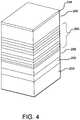
- Figure 4shows a layering arrangement that may be used on the absorptive plate 200.
- the face 203 of the absorptive plate 200 that faces the substrate 140 during processinghas a layer that is highly reflective of radiation in a target wavelength range and less reflective of radiation outside the target wavelength range.
- one or more coatings or layersare provided on the absorptive plate surface to achieve this selective reflectivity. In one embodiment, these coatings provide high reflectivity for radiation in the target wavelength range, and include one or more interference layers positioned over the surface of the absorptive plate.
- one or more interference layers 250are included in the layer structure.
- the interference layerscontain pairs of layers, each pair comprising a layer with a low index of refraction and a layer with a high index of refraction.
- the interference layerscomprise a structure that is highly reflective of radiation in the target wavelength range and less reflective of radiation outside the target wavelength range.
- the particular material, thickness, and other characteristics of the interference layersare selected based on a number of characteristics of the processing system, including the target wavelength range desired.
- a suitable interference layer structuremay be obtained from Research Electro-Optics, Inc, of Boulder, Colorado.
- a highly reflective portion of an absorptive plate 200comprises a quarter-wave stack.
- the quarter-wave stackis made up of alternating dielectric layers which have different indices of refraction and have optical thickness equal to 1/4 of the wavelength to which the pyrometer is most sensitive over the respective angles of acceptance into the pyrometer (e.g., a thickness equal to 1/4 of 950 nanometers).
- the interference layers 250provide high reflectivity for radiation in the target wavelength
- Another portion of the absorptive plate 200absorbs radiation outside the target wavelength.
- an absorptive layer 252can be positioned above the absorptive plate's face 203 and below the interference layers 250.
- This absorptive layer 250is more absorptive than the high reflectivity portion of the absorptive plate 200. As radiation outside the target wavelength passes through the interference layers, it is absorbed by the absorptive layers. The resultant heat passes through the absorptive plate 200 and is dissipated through the cooling mechanism described above.
- the absorbing layer 252including, for example, metal oxides, and suitable materials will be apparent to those of skill in the art.
- other mechanisms for absorption of radiationmay also be employed.
- the absorptive plate face 203may absorb radiation that passes through the highly reflective portion of absorptive plate.
- the structure of the interference layers 250 shown in Figure 4is merely exemplary; other mechanisms known in the art may be used to filter, mirror, or reflect radiation in the target wavelength range away from the absorbing portion of the absorptive plate 200.
- a passivation layer 254may be employed above the interference layers 250. This passivation layer prevents the material of the layers above the absorptive plate face 203 from possibly contaminating the chamber.
- the passivation layer 254may be made of silicon dioxide, aluminum oxide, silicon nitride, or any other acceptable material that will passivate the reflector without unacceptably degrading its reflective properties in the wavelength range of interest.
- layers 256, 258may be employed on the reflector surface within the scope of the present invention to perform well-known functions for the fabrication or operation of the device.
- such layers 256, 258may be employed to facilitate application of, or transition between, the absorbing layer 252, the interference layers 250, and/or the passivation layer 254.
- the target wavelength rangecorresponds to the spectral region that is used for the pyrometric temperature measurement.
- the pyrometric temperature measurementis an optical measurement of the radiation emitted by the substrate within a narrow spectral region. This spectral region is preferably approximately between 700 and 1000 nanometers.
- the wavelength of radiation to be absorbedcan also be identified.
- the spectrum of the radiated energy from a substrate during thermal processingis a complicated function of temperature, emissivity, and Planck's blackbody law. In simplified terms, the spectral limits of the absorbing portion of the reflector are determined by the blackbody law and the temperature range of the peak temperature of the process, i.e., the temperature of the process where radiative cooling is most desired.
- an absorptive plate 200has regions 205 of about one inch in diameter on each of the probes through which the temperature sensors, which are typically pyrometers, can measure the intensity of radiation over a predetermined wavelength region.
- the regions 205have very high reflectivity over the pyrometer wavelength range, which may be in the form of a multi-layer dielectric stack over a specular surface in the regions 205. The main importance of these regions is that they provide a local region where there is significant enhancement of the apparent emissivity of the wafer in the region as viewed by the pyrometer.
- the separation between the substrate and the plate 200is dependent on the desired thermal exposure for the given substrate.
- the substratecan be disposed at a greater distance from the plate 200 and closer to the lamps to increase the amount of thermal exposure of the substrate and to decrease the cooling from the plate.
- this configurationdecreases the amount of thermal exposure of the substrate and increases the cooling received from the plate.
- the exact position of the substrate during the heating of the substrate and the residence time spent in a specific positionis conditional on the desired amount of thermal exposure and amount of cooling. In most cases, the residence time is dependent on the desired surface chemistry of the substrate.
- the embodiment shown in FIG. 1allows the substrate support to be easily levitated at different vertical positions inside the chamber to permit control of the substrate's thermal exposure.
- the absorptive plate and light sourceare inverted from the configuration shown in Fig. 1 .
- the thermal conduction from the substrate to the absorptive plate 200will increase and enhance the cooling process.
- the increased rate of coolingin turn can promote optimal RTP performance.
- the amount of thermal exposure to the lampsdecreases while the amount of cooling from the plate increases.
- a gascan be released from a plurality of openings found on the surface of the absorptive plate to optimize cooling of the substrate.
- the plurality of openingsmay be configured to evenly distribute the gas across the radial surface of the substrate to enhance thermal conduction and convection between the substrate and the absorptive layer of the absorptive plate.
- a more conductive gasmay replace a less conductive gas, or the velocity of gas passing through holes 216 could be increased, creating turbulence and enhancing convective coupling between the showerhead and the substrate.
- Distributing gas radially towards the substrateoptimizes cooling of the substrate and optimizes spike performance of the RTP chamber.
- the substrate supportcan rotate the substrate to promote even distribution of gas over the substrate during processing for better uniformity.
- a method from thermally processing a substrate inside a RTP chamberinvolves positioning a substrate at a desired distance from the absorptive plate.
- the substratecan be easily moved to positions that are ideal for heating and cooling the substrate as set forth by the specifications for thermal processing.
- the substratemoves at different distances from the absorptive plate by utilizing the levitating support assembly described above.
- the support assemblycan be controlled by a CPU attached to the RTP chamber.
- a different set of gasescan be utilized during thermal processing.
- One set of gasesare used during the heating of the substrate and a second set of gases are used during the cooling of the substrate.
- the selections of gasesare dependent on the desired thermal conductivity. For example, using a low conductivity gas during thermal processing will decrease the amount of energy required during the ramp while using a gas of high thermal conductivity at the end of the process will increase the cool down rate.
- one or more embodiments of the inventionare directed to a rapid thermal processing (RTP) apparatus for heating a substrate.
- the RTP chambermay comprise a chamber and a support for holding the substrate in the chamber, the substrate having a first face and a second face opposite the first face.
- a radiant heat sourcewhich directs radiant energy towards the first face of the substrate may be inside the chamber.
- the radiant heat sourcecan be configured to be quickly turned on and off to controllably heat the substrate with a desired spatial temperature distribution, including a uniform distribution.
- the apparatusfurther includes at least one pyrometer for measuring the intensity of radiation over a predetermined wavelength range.
- the pyrometermay be positioned to receive radiation emitted by the substrate.
- the apparatusmight also include a plate which faces the second face of the substrate.
- the plateincludes at least one gas channel coupled to at least one gas source and to a plurality of openings on a surface of the plate. The openings are configured to evenly distribute process gases over the substrate.
- the platehas reflective regions that reflect radiation within the pre
- the platemay be positioned in close proximity to the substrate.
- the plate of these embodimentsmay absorb at least a portion of radiation emitted by the wafer.
- the plateextends over an area greater than that of the substrate.
- the gas channels of various embodimentsare configured to deliver a first gas and a second gas.
- the first and second gasesmay be mixed in at least one mixing chamber within the gas channels before being delivered. Additional configurations may allow for more than two gases to be delivered simultaneously.
- the gasesmay also be reactive, and can be mixed before or after delivery to the substrate surface. "Reactive gases" refer to gases that may be used for a reaction on the substrate such as an etching gas, or gases that are precursors that are used to form a material on the substrate.
- the platehas an outer, highly reflective portion, and an inner portion having an absorptive layer underlying the outer portion.
- the reflective regions of the platecan be positioned to reflect heat toward the at least one pyrometer.
- the openings of some embodimentsare configured to evenly distribute gas across a radial surface of the substrate to promote thermal coupling of the plate to the substrate. In other embodiments, the openings are distributed evenly across the plate.
- Some embodimentshave a support for mounting the substrate being a levitating support assembly.
- the levitating assemblycan be configured to move the substrate between an upper position and lower position within the chamber.
- the levitating support assemblycan also be magnetically coupled to a stator assembly.
- the stator assemblycan be further mechanically coupled to an actuator assembly.
- the substratecan be positioned at various distances from the plate during the heating and/or cooling processes. This may allow for custom tailoring the gas flow field between the plate and the substrate. The distance can be changed dynamically, thereby modulating the residence times of active species to affect the substrate surface chemistry.
- Additional embodiments of the inventionare directed toward methods for rapidly thermally processing a substrate.
- the methodmay include rapidly heating the substrate by directing a radiant heat source to a first surface of the substrate; reflecting the radiant heat towards a second surface of the substrate with a reflective body positioned proximate to a second surface the substrate; cooling the substrate by absorbing heat through an absorptive plate; and directing a process gas through the absorptive plate to the second surface of the substrate.
- the heating of the substratein some embodiments comprises a time period of about 2 minutes or less.
- the cooling of the substratein other embodiments may be done in a time period of about 10 seconds or less.
- the substrate of various embodimentsis positioned below and proximate the absorptive plate for cooling.
- Further embodimentsdirect the process gas through a plurality of openings on a surface of the absorptive plate.
- the openingsmay be positioned to evenly distribute gas across the radial surface of the substrate to enhance thermal conduction between the substrate and an absorptive layer of the absorptive plate during cooling.
- the openingsmay also be positioned to distribute gas across the radial surface of the substrate in a controlled uneven distribution.
- the rapid thermal processing technique of various embodimentscomprises a spike annealing process to form a film on the substrate.
Landscapes
- Chemical & Material Sciences (AREA)
- Engineering & Computer Science (AREA)
- Mechanical Engineering (AREA)
- General Chemical & Material Sciences (AREA)
- Chemical Kinetics & Catalysis (AREA)
- Materials Engineering (AREA)
- Metallurgy (AREA)
- Organic Chemistry (AREA)
- Physics & Mathematics (AREA)
- Condensed Matter Physics & Semiconductors (AREA)
- General Physics & Mathematics (AREA)
- Manufacturing & Machinery (AREA)
- Computer Hardware Design (AREA)
- Microelectronics & Electronic Packaging (AREA)
- Power Engineering (AREA)
- Health & Medical Sciences (AREA)
- Toxicology (AREA)
- General Engineering & Computer Science (AREA)
- Chemical Vapour Deposition (AREA)
Description
- Embodiments of the invention relate generally to heat treatment of semiconductor wafers and other substrates. In particular, embodiments of the invention relate to rapid thermal processing of wafers from a radiant source, such as an array of incandescent lamps.
- The fabrication of integrated circuits from silicon or other wafers involves many steps of depositing layers, photo lithographically patterning the layers, and etching the patterned layers. Ion implantation is used to dope active regions in the semiconductive silicon. The fabrication sequence also includes thermal annealing of the wafers for many uses including curing implant damage and activating the dopants, crystallization, thermal oxidation and nitridation, silicidation, chemical vapor deposition, vapor phase doping, thermal cleaning, and other reasons. Although annealing in early stages of silicon technology typically involved heating multiple wafers for long periods in an annealing oven, rapid thermal processing, (RTP) has been increasingly used to satisfy the ever more stringent requirements for ever smaller circuit features. RTP is typically performed in single-wafer chambers by irradiating a wafer with light from an array of high-intensity lamps directed at the front face of the wafer on which the integrated circuits are being formed. The radiation is at least partially absorbed by the wafer and quickly heats it to a desired high temperature, for example above 600° C, or in some applications, above 1000° C. The radiant heating can be quickly turned on and off to controllably and uniformly heat the wafer over a relatively short period, for example, of a minute or less, or even a few seconds. RTP chambers are capable of uniformly heating a wafer at rates of about 50° C/second and higher, for example, at rates of 100°-150° C/second, and 200°-400° C/second. Typical ramp-down (cooling) rates in RTP chambers are in the range of 80-150° C/second. Some processes performed in RTP chambers require variations in temperature across the substrate of less than a few degrees Celsius.
- Since rapid thermal processing works on a single semiconductor each time, optimal heating and cooling means are necessary for optimal RTP performance. It is desirable to optimize substrate temperature uniformity during thermal processing of the substrate. Temperature uniformity provides uniform process variables on the substrate (e.g. layer thickness, resistivity, etch depth) for temperature activated steps such as film deposition, oxide growth and etching. In addition, substrate temperature uniformity is necessary to prevent thermal stress-induced substrate damage such as warpage, defect generation and slip. For example, at 1150° C, a center to edge temperature difference on a four-inch silicon wafer of approximately 5° C can induce dislocation formation and slip. Temperature gradients may also be induced by other sources. For example, a substrate may have non-uniform emissivity because of spatial modifications to surface areas or volumes of the substrate. These modifications may include films that have been patterned by photolithography or locally doped regions, such as buried layers for bipolar transistors. In addition, substrate temperature gradients may be induced by localized gas cooling or heating effects related to processing chamber design as well as non-uniform endothermic or exothermic reactions that may occur on the substrate surface during processing. It would be desirable to provide RTP chambers that provide improved temperature uniformity.
US 5 595 606 describes a metal CVD apparatus including a process chamber, a work table for mounting a wafer thereon, heating lamps, and a shower head for supplying a process gas into the process chamber. The shower head includes spreading outlets.WO 2005/093353 A1 describes an RTP reactor including a process area for processing a wafer. The RTP reactor includes a shelf for supporting the wafer, radiant lamps, pyrometers, and a reflector to reflect heat radiation emitted from the wafer back toward the wafer.EP 1 933 368 describes an RTP chamber including a substrate support, a radiant heat source, and pyrometers. - One or more embodiments of the invention are directed to a rapid thermal processing (RTP) apparatus for heating a substrate. The RTP chamber may comprise a chamber and a support for holding the substrate in the chamber, the substrate having a first face and a second face opposite the first face. A radiant heat source which directs radiant energy towards the first face of the substrate may be inside the chamber. The radiant heat source can be configured to be quickly turned on and off to controllably heat the substrate with a desired spatial temperature distribution, including a uniform distribution. The apparatus further includes at least one pyrometer for measuring the intensity of radiation over a predetermined wavelength range. The pyrometer may be positioned to receive radiation emitted by the substrate. The apparatus may also include a plate which faces the second face of the substrate. The plate includes at least one gas channel coupled to at least one gas source and to a plurality of openings on a surface of the plate. The openings are configured to evenly distribute process gases over the substrate. The plate has reflective regions that reflect radiation within the predetermined wavelength range.
- In other embodiments, the plate may be positioned in close proximity to the substrate. The plate of these embodiments may absorb at least a portion of radiation emitted by the substrate. In further embodiments, the plate extends over an area greater than that of the substrate.
- In one or more embodiments, the gas channels are configured to deliver a first gas and a second gas. The first and second gases may be mixed in at least one mixing chamber within the gas channels before being delivered. Additional configurations may allow for more than two gases to be delivered simultaneously. The gases may also be reactive, and can be mixed before or after delivery to the substrate surface.
- In further embodiments, the plate has an outer, highly reflective portion, and an inner portion having an absorptive layer underlying the outer portion. The reflective regions of the plate can be positioned to reflect heat toward the at least one pyrometer.
- The openings of some embodiments are configured to evenly distribute gas across a radial surface of the substrate to promote thermal coupling of the plate to the substrate. In other embodiments, the openings are distributed evenly across the plate.
- Some embodiments have a support for mounting the substrate being a levitating support assembly. The levitating assembly can be configured to move the substrate between an upper position and lower position within the chamber. The levitating support assembly can also be magnetically coupled to a stator assembly. The stator assembly can be further mechanically coupled to an actuator assembly.
- In one or more embodiments, the substrate can be positioned at various distances from the plate during the heating a cooling processes. This may allow for custom tailoring the gas flow field between the plate and the substrate. The distance can be changed dynamically, thereby modulating the residence times of active species to affect the substrate surface chemistry.
- Additional embodiments of the invention are directed toward methods for rapidly thermally processing a substrate. The method may include rapidly heating the substrate by directing a radiant heat source to a first surface of the substrate; reflecting the radiant heat towards a second surface of the substrate with a reflective body positioned proximate to a second surface the substrate; cooling the substrate by absorbing heat through an absorptive plate; directing a process gas through the absorptive plate to the second surface of the substrate; measuring the intensity of radiation over a predetermined temperature range; and reflecting radiation within the predetermined wavelength range by reflective regions of the absorptive plate.
- The heating of the substrate in some embodiments comprises a time period of about 2 minutes or less. The cooling of the substrate in other embodiments may be done in a time period of about 10 seconds or less. In one or more embodiments, the substrate is positioned below and proximate the plate for cooling. In other embodiments, the substrate is positioned above the plate.
- Further embodiments direct the process gas through a plurality of openings on a surface of the absorptive plate. The openings may be positioned to evenly distribute gas across the radial surface of the substrate to enhance thermal conduction between the substrate and an absorptive layer of the absorptive plate during cooling. The openings may also be positioned to distribute gas across the radial surface of the substrate in a controlled uneven distribution.
- The rapid thermal processing technique of various embodiments comprises a spike annealing process to form a film on the substrate.
FIG. 1 is a simplified isometric view of an embodiment of a rapid thermal processing (RTP) chamber;FIG. 2 is a cross-sectional view of a substrate positioned proximate an absorptive shower head according to an embodiment;FIG. 3 is a bottom plan view of the absorptive shower head; andFIG. 4 is a cross-sectional view taken along line 3-3 inFig 2 .- The embodiments described below are generally directed to an RTP system including a plate incorporating gas distribution outlets to distribute gas evenly over a substrate to allow rapid and controlled heating and cooling of the substrate. The plate may be absorptive, reflective, or a combination of both. As used herein, rapid thermal processing or RTP refers an apparatus or a process capable of uniformly heating a wafer at rates of about 50 °C/second and higher, for example, at rates of 100 to 150° C/second, and 200 to 400° C/second. Typical ramp-down (cooling) rates in RTP chambers are in the range of 80-150° C/second. Some processes performed in RTP chambers require variations in temperature across the substrate of less than a few degrees Celsius. Thus, an RTP chamber must include a lamp or other suitable heating system and heating system control capable of heating at rates of up to 100 to 150° C/second, and 200 to 400° C/second distinguishing rapid thermal processing chambers from other types of thermal chambers that do not have a heating system and heating control system capable of rapidly heating at these rates. In the embodiment shown, the RTP chamber optionally includes a substrate support that is adapted to levitate and rotate within the
chamber without any contact with the inside walls of the chamber. The levitating substrate support system, coupled with the absorptive plate incorporating gas distribution outlets, enables the flow from the absorptive plate to be tailored to enhance heating and cooling of the substrate being processed in the chamber. By providing the ability to modulate the distance between the absorptive plate with the gas distribution outlets, the residence time of active species can be changed and the substrate surface chemistry can be more accurately changed. - Referring now to
FIG. 1 , an exemplary embodiment of a rapidthermal processing chamber 100 is shown. Theprocessing chamber 100 includes asubstrate support 104, achamber body 102, havingwalls 108, a bottom 110, and a top 112 defining aninterior volume 120. Thewalls 108 typically include at least onesubstrate access port 148 to facilitate entry and egress of a substrate 140 (a portion of which is shown inFigure 1 ). The access port may be coupled to a transfer chamber (not shown) or a load lock chamber (not shown) and may be selectively sealed with a valve, such as a slit valve (not shown). In one embodiment, thesubstrate support 104 is annular and thechamber 100 includes aradiant heat source 106 disposed in an inside diameter of thesubstrate support 104. Theradiant heat source 106 typically comprises a plurality of lamps. Examples of an RTP chamber that may be modified and a substrate support that may be used is described in United States Patent No.6,800,833 and United States Patent Application Publication No.2005/0191044 , both of which are incorporated by reference in their entireties. In one embodiment of the invention, thechamber 100 includes aplate 200 incorporating gas distribution outlets (described in more detail below) to distribute gas evenly over a substrate to allow rapid and controlled heating and cooling of the substrate. - The plate may be absorptive, reflective, or have a combination of absorptive and reflective regions. In a detailed embodiment, the plate may have regions, some within view of the pyrometers, some outside the view of the pyrometers. The regions within view of the pyrometers may be about one inch in diameter, if circular, or other shape and size as necessary. The regions within view of the probes may be very highly reflective over the wavelength ranges observed by the pyrometers. Outside the pyrometer wavelength range and field of view, the plate can range from reflective to minimize radiative heat loss, to absorptive to maximize radiative heat loss to allow for shorter thermal exposure.
- The
RTP chamber 100 also includes acooling block 180 adjacent to, coupled to, or formed in the top 112. Generally, thecooling block 180 is spaced apart and opposing theradiant heat source 106. Thecooling block 180 comprises one ormore coolant channels 184 coupled to aninlet 181A and anoutlet 181 B. Thecooling block 180 may be made of a process resistant material, such as stainless steel, aluminum, a polymer, or a ceramic material. Thecoolant channels 184 may comprise a spiral pattern, a rectangular pattern, a circular pattern, or combinations thereof and thechannels 184 may be formed integrally within thecooling block 180, for example by casting thecooling block 180 and/or fabricating thecooling block 180 from two or more pieces and joining the pieces. Additionally or alternatively, thecoolant channels 184 may be drilled into thecooling block 180. - The
inlet 181A andoutlet 181B may be coupled to acoolant source 182 by valves and suitable plumbing and thecoolant source 182 is in communication with thecontroller 124 to facilitate control of pressure and/or flow of a fluid disposed therein. The fluid may be water, ethylene glycol, nitrogen (N2), helium (He), or other fluid used as a heat-exchange medium. - In the embodiment shown, the
substrate support 104 is optionally adapted to magnetically levitate and rotate within theinterior volume 120. Thesubstrate support 104 shown is capable of rotating while raising and lowering vertically during processing, and may also be raised or lowered without rotation before, during, or after processing. This magnetic levitation and/or magnetic rotation prevents or minimizes particle generation due to the absence or reduction of moving parts typically required to raise/lower and/or rotate the substrate support. - The
chamber 100 also includes awindow 114 made from a material transparent to heat and light of various wavelengths, which may include light in the infra-red (IR) spectrum, through which photons from theradiant heat source 106 may heat thesubstrate 140. In one embodiment, thewindow 114 is made of a quartz material, although other materials that are transparent to light maybe used, such as sapphire. Thewindow 114 may also include a plurality of lift pins 144 coupled to an upper surface of thewindow 114, which are adapted to selectively contact and support thesubstrate 140, to facilitate transfer of the substrate into and out of thechamber 100. Each of the plurality of lift pins 144 are configured to minimize absorption of energy from theradiant heat source 106 and may be made from the same material used for thewindow 114, such as a quartz material. The plurality of lift pins 144 may be positioned and radially spaced from each other to facilitate passage of an end effector coupled to a transfer robot (not shown). Alternatively, the end effector and/or robot may be capable of horizontal and vertical movement to facilitate transfer of thesubstrate 140. - In one embodiment, the
radiant heat source 106 includes a lamp assembly formed from a housing which includes a plurality ofhoneycomb tubes 160 in a coolant assembly (not shown) coupled to asecond coolant source 183. Thesecond coolant source 183 may be one or a combination of water, ethylene glycol, nitrogen (N2), and helium (He). Thehousing walls second coolant source 183. The coolant cools the housing of thechamber 100 so that the housing is cooler than thesubstrate 140. Eachtube 160 may contain a reflector and a high-intensity lamp assembly or an IR emitter from which is formed a honeycomb like pipe arrangement. This close-packed hexagonal arrangement of pipes provides radiant energy sources with high power density and good spatial resolution. In one embodiment, theradiant heat source 106 provides sufficient radiant energy to thermally process the substrate, for example, annealing a silicon layer disposed on thesubstrate 140. Theradiant heat source 106 may further comprise annular zones, wherein the voltage supplied to the plurality oftubes 160 bycontroller 124 may varied to enhance the radial distribution of energy from thetubes 160. Dynamic control of the heating of thesubstrate 140 may be effected by the one ormore temperature sensors 117 adapted to measure the temperature across thesubstrate 140. - In the embodiment shown, an
optional stator assembly 118 circumscribes thewalls 108 of thechamber body 102 and is coupled to one ormore actuator assemblies 122 that control the elevation of thestator assembly 118 along the exterior of thechamber body 102. In one embodiment (not shown), thechamber 100 includes threeactuator assemblies 122 disposed radially about the chamber body, for example, at about 120°angles about thechamber body 102. Thestator assembly 118 is magnetically coupled to thesubstrate support 104 disposed within theinterior volume 120 of thechamber body 102. Thesubstrate support 104 may comprise or include a magnetic portion to function as a rotor, thus creating a magnetic bearing assembly to lift and/or rotate thesubstrate support 104. In one embodiment, at least a portion of thesubstrate support 104 is partially surrounded by a trough (not shown) that is coupled to afluid source 186, which may include water, ethylene glycol, nitrogen (N2), helium (He), or combinations thereof, adapted as a heat exchange medium for the substrate support. Thestator assembly 118 may also include ahousing 190 to enclose various parts and components of thestator assembly 118. In one embodiment, thestator assembly 118 includes adrive coil assembly 168 stacked on asuspension coil assembly 170. Thedrive coil assembly 168 is adapted to rotate and/or raise/lower thesubstrate support 104 while thesuspension coil assembly 170 may be adapted to passively center thesubstrate support 104 within theprocessing chamber 100. Alternatively, the rotational and centering functions may be performed by a stator having a single coil assembly. - An
atmosphere control system 164 is also coupled to theinterior volume 120 of thechamber body 102. Theatmosphere control system 164 generally includes throttle valves and vacuum pumps for controlling chamber pressure. Theatmosphere control system 164 may additionally include gas sources for providing process or other gases to theinterior volume 120. Theatmosphere control system 164 may also be adapted to deliver process gases for thermal deposition processes, thermal etch processes, and in-situ cleaning of chamber components. The atmosphere control system works in conjunction with the showerhead gas delivery system. - The
chamber 100 also includes acontroller 124, which generally includes a central processing unit (CPU) 130,support circuits 128 andmemory 126. TheCPU 130 may be one of any form of computer processor that can be used in an industrial setting for controlling various actions and sub-processors. Thememory 126, or computer-readable medium, may be one or more of readily available memory such as random access memory (RAM), read only memory (ROM), floppy disk, hard disk, or any other form of digital storage, local or remote, and is typically coupled to theCPU 130. Thesupport circuits 128 are coupled to theCPU 130 for supporting thecontroller 124 in a conventional manner. These circuits include cache, power supplies, clock circuits, input/output circuitry, subsystems, and the like. - In one embodiment, each of the
actuator assemblies 122 generally comprise aprecision lead screw 132 coupled between twoflanges 134 extending from thewalls 108 of thechamber body 102. Thelead screw 132 has anut 158 that axially travels along thelead screw 132 as the screw rotates. Acoupling 136 is coupled between thestator 118 andnut 158 so that as thelead screw 132 is rotated, thecoupling 136 is moved along thelead screw 132 to control the elevation of thestator 118 at the interface with thecoupling 136. Thus, as thelead screw 132 of one of theactuators 122 is rotated to produce relative displacement between thenuts 158 of theother actuators 122, the horizontal plane of thestator 118 changes relative to a central axis of thechamber body 102. - In one embodiment, a
motor 138, such as a stepper or servo motor, is coupled to thelead screw 132 to provide controllable rotation in response to a signal by thecontroller 124. Alternatively, other types ofactuators 122 may be utilized to control the linear position of thestator 118, such as pneumatic cylinders, hydraulic cylinders, ball screws, solenoids, linear actuators and cam followers, among others. - The
chamber 100 also includes one ormore sensors 116, which are generally adapted to detect the elevation of the substrate support 104 (or substrate 140) within theinterior volume 120 of thechamber body 102. Thesensors 116 may be coupled to thechamber body 102 and/or other portions of theprocessing chamber 100 and are adapted to provide an output indicative of the distance between thesubstrate support 104 and the top 112 and/orbottom 110 of thechamber body 102, and may also detect misalignment of thesubstrate support 104 and/orsubstrate 140. - The one or
more sensors 116 are coupled to thecontroller 124 that receives the output metric from thesensors 116 and provides a signal or signals to the one ormore actuator assemblies 122 to raise or lower at least a portion of thesubstrate support 104. Thecontroller 124 may utilize a positional metric obtained from thesensors 116 to adjust the elevation of thestator 118 at eachactuator assembly 122 so that both the elevation and the planarity of thesubstrate support 104 andsubstrate 140 seated thereon may be adjusted relative to and a central axis of theRTP chamber 100 and/or theradiant heat source 106. For example, thecontroller 124 may provide signals to raise the substrate support by action of oneactuator 122 to correct axial misalignment of thesubstrate support 104, or the controller may provide. a signal to allactuators 122 to facilitate simultaneous vertical movement of thesubstrate support 104. - The one or
more sensors 116 may be ultrasonic, laser, inductive, capacitive, or other type of sensor capable of detecting the proximity of thesubstrate support 104 within thechamber body 102. Thesensors 116, may be coupled to thechamber body 102 proximate the top 112 or coupled to thewalls 108, although other locations within and around thechamber body 102 may be suitable, such as coupled to thestator 118 outside of thechamber 100. In one embodiment, one ormore sensors 116 may be coupled to thestator 118 and are adapted to sense the elevation and/or position of the substrate support 104 (or substrate 140) through thewalls 108. In this embodiment, thewalls 108 may include a thinner cross-section to facilitate positional sensing through thewalls 108. - The
chamber 100 also includes one ormore temperature sensors 117, which may be adapted to sense temperature of thesubstrate 140 before, during, and after processing. In the embodiment depicted inFigure 1 , thetemperature sensors 117 are disposed through the top 112, although other locations within and around thechamber body 102 may be used. Thetemperature sensors 117 may be optical pyrometers, as an example, pyrometers having fiber optic probes. Thesensors 117 may be adapted to couple to the top 112 in a configuration to sense the entire diameter of the substrate, or a portion of the substrate. Thesensors 117 may comprise a pattern defining a sensing area substantially equal to the diameter of the substrate, or a sensing area substantially equal to the radius of the substrate. For example, a plurality ofsensors 117 may be coupled to the top 112 in a radial or linear configuration to enable a sensing area across the radius or diameter of the substrate. In one embodiment (not shown), a plurality ofsensors 117 may be disposed in a line extending radially from about the center of the top 112 to a peripheral portion of the top 112. In this manner, the radius of the substrate may be monitored by thesensors 117, which will enable sensing of the diameter of the substrate during rotation. - As described herein, the
chamber 100 is adapted to receive a substrate in a "face-up" orientation, wherein the deposit receiving side or face of the substrate is oriented toward theplate 200 and the "backside" of the substrate is facing theradiant heat source 106. The "face-up" orientation may allow the energy from theradiant heat source 106 to be absorbed more rapidly by thesubstrate 140 as the backside of the substrate is typically less reflective than the face of the substrate. - Although the
plate 200 andradiant heat source 106 is described as being positioned in an upper and lower portion of theinterior volume 120, respectively, the position of thecooling block 180 and theradiant heat source 106 may be reversed. For example, thecooling block 180 may be sized and configured to be positioned within the inside diameter of thesubstrate support 104, and theradiant heat source 106 may be coupled to the top 112. In this arrangement, thequartz window 114 may be disposed between theradiant heat source 106 and thesubstrate support 104, such as adjacent theradiant heat source 106 in the upper portion of thechamber 100. Although thesubstrate 140 may absorb heat readily when the backside is facing the radiant heat -source 106, thesubstrate 140 could be oriented in a face-up orientation or a face down orientation in either configuration. - Further details on an
absorptive plate 200 are shown inFigures 2 and3 . Referring toFigure 2 , anabsorptive plate 200 incorporating gas distribution outlets to distribute gas evenly over a substrate to allow rapid and controlled heating and cooling of the substrate is shown. Theplate 200 includes atop portion 201 having agas introduction system 202, includes a firstgas introduction port 204 and an optional secondgas introduction port 206 in communication with agas mixing chamber 208 for mixing gases the two gases. If only a single gas introduction port is provided, mixingchamber 208 can be eliminated from the design. It will be understood that additional gas introduction ports can be provided as well. Thegas introduction ports chamber 208 is in communication withgas flow passage 212, which is in communication withgas channel 214 andgas introduction openings 216 formed inblocker plate 213. Theblocker plate 213 may be a separate component fastened to thetop portion 201, or it may be integrally formed with the top portion. Of course, other designs are possible, including ones where two or more sets of individual openings of thetype 216 are provided for two or more gases so that gas mixing takes place after exiting the showerhead. The absorptive plate includes aface 203 through whichopenings 216 are formed. Figure 3 shows a plan view of anabsorptive plate 200 and the plurality ofopenings 216 throughface 203. It will be understood that the number of and pattern of openings can be varied and the design shown inFigure 3 is exemplary only. For ease of illustration, bores through theplate 200 to allow thetemperature sensors 117 to measure the temperature of the substrate. In one or more embodiments, the plurality of openings on the absorptive plate comprise of no more than 10% of the plate's surface. In one embodiment the plurality of openings are positioned no closer than within a 25mm of the pyrometers and within a 1 in diameter of the highly reflective surface of the absorptive plate.- In one or more embodiments, in a system for processing silicon substrates, a pyrometer that detects long radiation wavelengths (e.g., wavelengths greater than about 3.5 to 4 microns) is utilized as the
temperature sensor 117. However, this approach is best suited for temperatures above 700° C. At room temperature, a silicon wafer is transparent to wavelengths of light longer than 1.0 microns. As the temperature of the substrate increases, the substrate becomes opaque to the longer wavelengths until, at about 700° C, the substrate becomes opaque to all wavelengths of interest. Thus, at temperatures below 700° C, a long wavelength sensitive pyrometer will be more apt to also detect light coming directly from the heat source. In short, the wavelength sampled by the pyrometer will typically vary with the process temperature. If the process temperature is substantially below 700° C, then the pyrometer will typically sample wavelengths shorter than 1.1 microns. If higher process temperatures are used, then longer wavelengths can be sampled. - In one design, particularly suitable for process temperatures between 900° C and 1350° C, a solid-state pyrometer is used that is sensitive to radiation at wavelengths between 0.9 microns and 1.0 microns. In this temperature range, there is substantial amount of radiation produced in the wavelength range 0.9-1.0 microns providing high signal strengths and high signal-to-noise ratios.
Figure 4 shows a layering arrangement that may be used on theabsorptive plate 200. As shown inFigure 4 , theface 203 of theabsorptive plate 200 that faces thesubstrate 140 during processing has a layer that is highly reflective of radiation in a target wavelength range and less reflective of radiation outside the target wavelength range. In some embodiments, one or more coatings or layers are provided on the absorptive plate surface to achieve this selective reflectivity. In one embodiment, these coatings provide high reflectivity for radiation in the target wavelength range, and include one or more interference layers positioned over the surface of the absorptive plate.- As shown in
Figure 3 , one or more interference layers 250 are included in the layer structure. The interference layers contain pairs of layers, each pair comprising a layer with a low index of refraction and a layer with a high index of refraction. Together, the interference layers comprise a structure that is highly reflective of radiation in the target wavelength range and less reflective of radiation outside the target wavelength range. The particular material, thickness, and other characteristics of the interference layers are selected based on a number of characteristics of the processing system, including the target wavelength range desired. A suitable interference layer structure may be obtained from Research Electro-Optics, Inc, of Boulder, Colorado. - In one embodiment, a highly reflective portion of an
absorptive plate 200 comprises a quarter-wave stack. The quarter-wave stack is made up of alternating dielectric layers which have different indices of refraction and have optical thickness equal to 1/4 of the wavelength to which the pyrometer is most sensitive over the respective angles of acceptance into the pyrometer (e.g., a thickness equal to 1/4 of 950 nanometers). As noted above, the interference layers 250 provide high reflectivity for radiation in the target wavelength Another portion of theabsorptive plate 200 absorbs radiation outside the target wavelength. In one embodiment, anabsorptive layer 252 can be positioned above the absorptive plate'sface 203 and below the interference layers 250. Thisabsorptive layer 250 is more absorptive than the high reflectivity portion of theabsorptive plate 200. As radiation outside the target wavelength passes through the interference layers, it is absorbed by the absorptive layers. The resultant heat passes through theabsorptive plate 200 and is dissipated through the cooling mechanism described above. - Various materials may be employed for the
absorbing layer 252 including, for example, metal oxides, and suitable materials will be apparent to those of skill in the art. Moreover, other mechanisms for absorption of radiation may also be employed. For example, rather than employing anabsorbing layer 252 as shown inFigure 4 , theabsorptive plate face 203 may absorb radiation that passes through the highly reflective portion of absorptive plate. Likewise, the structure of the interference layers 250 shown inFigure 4 is merely exemplary; other mechanisms known in the art may be used to filter, mirror, or reflect radiation in the target wavelength range away from the absorbing portion of theabsorptive plate 200. - As shown in
Figure 4 , apassivation layer 254 may be employed above the interference layers 250. This passivation layer prevents the material of the layers above theabsorptive plate face 203 from possibly contaminating the chamber. Thepassivation layer 254 may be made of silicon dioxide, aluminum oxide, silicon nitride, or any other acceptable material that will passivate the reflector without unacceptably degrading its reflective properties in the wavelength range of interest. Other layers such layers layer 252, the interference layers 250, and/or thepassivation layer 254.- Generally the target wavelength range corresponds to the spectral region that is used for the pyrometric temperature measurement. In one embodiment, the pyrometric temperature measurement is an optical measurement of the radiation emitted by the substrate within a narrow spectral region. This spectral region is preferably approximately between 700 and 1000 nanometers. Similarly, the wavelength of radiation to be absorbed can also be identified. The spectrum of the radiated energy from a substrate during thermal processing is a complicated function of temperature, emissivity, and Planck's blackbody law. In simplified terms, the spectral limits of the absorbing portion of the reflector are determined by the blackbody law and the temperature range of the peak temperature of the process, i.e., the temperature of the process where radiative cooling is most desired.
- In a detailed embodiment, shown in
Figure 3 , anabsorptive plate 200 hasregions 205 of about one inch in diameter on each of the probes through which the temperature sensors, which are typically pyrometers, can measure the intensity of radiation over a predetermined wavelength region. Theregions 205 have very high reflectivity over the pyrometer wavelength range, which may be in the form of a multi-layer dielectric stack over a specular surface in theregions 205. The main importance of these regions is that they provide a local region where there is significant enhancement of the apparent emissivity of the wafer in the region as viewed by the pyrometer. - In the embodiment shown in
FIG. 1 , the separation between the substrate and theplate 200 is dependent on the desired thermal exposure for the given substrate. In one embodiment, the substrate can be disposed at a greater distance from theplate 200 and closer to the lamps to increase the amount of thermal exposure of the substrate and to decrease the cooling from the plate. When the substrate is placed at position closer to theplate 200 and further from the lamps, this configuration decreases the amount of thermal exposure of the substrate and increases the cooling received from the plate. The exact position of the substrate during the heating of the substrate and the residence time spent in a specific position is conditional on the desired amount of thermal exposure and amount of cooling. In most cases, the residence time is dependent on the desired surface chemistry of the substrate. The embodiment shown inFIG. 1 allows the substrate support to be easily levitated at different vertical positions inside the chamber to permit control of the substrate's thermal exposure. - In an alternative embodiment, the absorptive plate and light source are inverted from the configuration shown in
Fig. 1 . In the inverted configuration, when the substrate is proximate the absorptive plate, the thermal conduction from the substrate to theabsorptive plate 200 will increase and enhance the cooling process. The increased rate of cooling in turn can promote optimal RTP performance. Thus, when the substrate is positioned closer to the absorptive plate, the amount of thermal exposure to the lamps decreases while the amount of cooling from the plate increases. - In one embodiment, as the substrate is moved into a position proximate an absorptive plate, a gas can be released from a plurality of openings found on the surface of the absorptive plate to optimize cooling of the substrate. The plurality of openings may be configured to evenly distribute the gas across the radial surface of the substrate to enhance thermal conduction and convection between the substrate and the absorptive layer of the absorptive plate. To enhance the conductive effects, a more conductive gas may replace a less conductive gas, or the velocity of gas passing through
holes 216 could be increased, creating turbulence and enhancing convective coupling between the showerhead and the substrate. Distributing gas radially towards the substrate optimizes cooling of the substrate and optimizes spike performance of the RTP chamber. In some embodiments, the substrate support can rotate the substrate to promote even distribution of gas over the substrate during processing for better uniformity. - A method from thermally processing a substrate inside a RTP chamber involves positioning a substrate at a desired distance from the absorptive plate. The substrate can be easily moved to positions that are ideal for heating and cooling the substrate as set forth by the specifications for thermal processing. The substrate moves at different distances from the absorptive plate by utilizing the levitating support assembly described above. In one embodiment, the support assembly can be controlled by a CPU attached to the RTP chamber.
- In another embodiment, a different set of gases can be utilized during thermal processing. One set of gases are used during the heating of the substrate and a second set of gases are used during the cooling of the substrate. The selections of gases are dependent on the desired thermal conductivity. For example, using a low conductivity gas during thermal processing will decrease the amount of energy required during the ramp while using a gas of high thermal conductivity at the end of the process will increase the cool down rate.
- Accordingly, one or more embodiments of the invention are directed to a rapid thermal processing (RTP) apparatus for heating a substrate. The RTP chamber may comprise a chamber and a support for holding the substrate in the chamber, the substrate having a first face and a second face opposite the first face. A radiant heat source which directs radiant energy towards the first face of the substrate may be inside the chamber. The radiant heat source can be configured to be quickly turned on and off to controllably heat the substrate with a desired spatial temperature distribution, including a uniform distribution. The apparatus further includes at least one pyrometer for measuring the intensity of radiation over a predetermined wavelength range. The pyrometer may be positioned to receive radiation emitted by the substrate. The apparatus might also include a plate which faces the second face of the substrate. The plate includes at least one gas channel coupled to at least one gas source and to a plurality of openings on a surface of the plate. The openings are configured to evenly distribute process gases over the substrate. The plate has reflective regions that reflect radiation within the predetermined wavelength range.
- In other embodiments, the plate may be positioned in close proximity to the substrate. The plate of these embodiments may absorb at least a portion of radiation emitted by the wafer. In further embodiments, the plate extends over an area greater than that of the substrate.
- The gas channels of various embodiments are configured to deliver a first gas and a second gas. The first and second gases may be mixed in at least one mixing chamber within the gas channels before being delivered. Additional configurations may allow for more than two gases to be delivered simultaneously. The gases may also be reactive, and can be mixed before or after delivery to the substrate surface. "Reactive gases" refer to gases that may be used for a reaction on the substrate such as an etching gas, or gases that are precursors that are used to form a material on the substrate.
- In further embodiments, the plate has an outer, highly reflective portion, and an inner portion having an absorptive layer underlying the outer portion. The reflective regions of the plate can be positioned to reflect heat toward the at least one pyrometer.
- The openings of some embodiments are configured to evenly distribute gas across a radial surface of the substrate to promote thermal coupling of the plate to the substrate. In other embodiments, the openings are distributed evenly across the plate.
- Some embodiments have a support for mounting the substrate being a levitating support assembly. The levitating assembly can be configured to move the substrate between an upper position and lower position within the chamber. The levitating support assembly can also be magnetically coupled to a stator assembly. The stator assembly can be further mechanically coupled to an actuator assembly.
- In one or more embodiments, the substrate can be positioned at various distances from the plate during the heating and/or cooling processes. This may allow for custom tailoring the gas flow field between the plate and the substrate. The distance can be changed dynamically, thereby modulating the residence times of active species to affect the substrate surface chemistry.
- Additional embodiments of the invention are directed toward methods for rapidly thermally processing a substrate. The method may include rapidly heating the substrate by directing a radiant heat source to a first surface of the substrate; reflecting the radiant heat towards a second surface of the substrate with a reflective body positioned proximate to a second surface the substrate; cooling the substrate by absorbing heat through an absorptive plate; and directing a process gas through the absorptive plate to the second surface of the substrate.
- The heating of the substrate in some embodiments comprises a time period of about 2 minutes or less. The cooling of the substrate in other embodiments may be done in a time period of about 10 seconds or less.
- The substrate of various embodiments is positioned below and proximate the absorptive plate for cooling.
- Further embodiments direct the process gas through a plurality of openings on a surface of the absorptive plate. The openings may be positioned to evenly distribute gas across the radial surface of the substrate to enhance thermal conduction between the substrate and an absorptive layer of the absorptive plate during cooling. The openings may also be positioned to distribute gas across the radial surface of the substrate in a controlled uneven distribution.
- The rapid thermal processing technique of various embodiments comprises a spike annealing process to form a film on the substrate.
- Reference throughout this specification to "one embodiment," "certain embodiments," "one or more embodiments" or "an embodiment" means that a particular feature, structure, material, or characteristic described in connection with the embodiment is included in at least one embodiment of the invention. Thus, the appearances of the phrases such as "in one or more embodiments," "in certain embodiments," "in one embodiment" or "in an embodiment" in various places throughout this specification are not necessarily referring to the same embodiment of the invention. Furthermore, the particular features, structures, materials, or characteristics may be combined in any suitable manner in one or more embodiments.
- Although the invention herein has been described with reference to particular embodiments, it is to be understood that these embodiments are merely illustrative of the principles and applications of the present invention. It will be apparent to those skilled in the art that various modifications and variations can be made to the method and apparatus of the present invention without departing from the scope of the invention. Thus, it is intended that the present invention include modifications and variations that are within the scope of the appended claims and their equivalents.
Claims (15)
- A rapid thermal processing apparatus (100) for heating a substrate (140), comprising:a chamber (102);a support (104) for holding the substrate in the chamber, the substrate having a first face and a second face opposite the first face;a radiant heat source (106) directing radiant energy towards the first face of the substrate and configured to be quickly turned on and off to controllably heat the substrate with a desired spatial temperature distribution, including a uniform distribution;at least one pyrometer (117) for measuring the intensity of radiation over a predetermined wavelength range, the pyrometer being positioned to receive radiation emitted by the substrate; anda plate (200) facing the second face of the substrate, the plate including at least one gas channel (202, 204, 212, 214) coupled to at least one gas source and to a plurality of openings (216) on a surface (203) of the plate configured to evenly distribute process gases over the substrate, the plate having reflective regions (205) that reflect radiation within the predetermined wavelength range.
- The apparatus of claim 1, wherein the plate is positioned in close proximity to the substrate and the plate absorbs at least a portion of radiation emitted by the substrate.
- The apparatus of claim 1, wherein the plate extends over an area greater than that of the substrate.
- The apparatus of claim 1, wherein the gas channels are configured to deliver a first gas and a second gas and the first gas and the second gas are mixed in at least one mixing chamber (208) within the gas channels and at least one of the first and second the gases are reactive.
- The apparatus of claim 1, wherein the plate has an outer, highly reflective portion (250), and an inner portion having an absorptive layer (252) underlying said outer portion.
- The apparatus of claim 5, wherein the openings that are configured to evenly distribute gas across a radial surface of the substrate promote thermal coupling of the plate to the substrate.
- The apparatus of claim 1, wherein the openings are distributed evenly across the plate.
- The apparatus of claim 1, wherein the support for mounting the substrate is a levitating support assembly configured to move the substrate between an upper position and lower position within the chamber and the levitating support assembly is magnetically coupled to a stator assembly (118) and the stator assembly is mechanically coupled to an actuator assembly (122).
- The apparatus of claim 1, wherein the reflective regions of the plate are positioned to reflect heat toward at least one pyrometer.
- A method for thermally processing a substrate (140) rapidly, comprising:rapidly heating the substrate by directing a radiant heat source (106) to a first surface of the substrate;reflecting the radiant heat towards a second surface of the substrate with a reflective body (250) positioned proximate to a second surface the substrate;cooling the substrate by absorbing heat through an absorptive plate (200);directing a process gas through the absorptive plate to the second surface of the substrate;measuring the intensity of radiation over a predetermined temperature range; andreflecting radiation within the predetermined wavelength range by reflective regions (205) of the absorptive plate.
- The method of claim 10, wherein the substrate is supported by a levitating and rotating substrate support (104) positioned in a chamber (102), the substrate is disposed above and proximate the radiant heat source for heating, and the substrate and the absorptive plate are separated by different distances during heating and cooling.
- The method of claim 11, wherein the heating comprises a time period of about 2 minutes or less, and the substrate is positioned below and proximate the absorptive plate for cooling, and the cooling comprises a time period of about 10 seconds or less.
- The method of claim 10, wherein the process gas is directed through a plurality of openings (216) on a surface (203) of the absorptive plate.
- The method of claim 13, wherein the openings are positioned to evenly distribute gas across the radial surface of the substrate to enhance thermal conduction between the substrate and an absorptive layer (252) of the absorptive plate during cooling.
- The method of claim 13, wherein the openings are positioned to distribute gas across the radial surface of the substrate in a controlled uneven distribution.
Applications Claiming Priority (2)
| Application Number | Priority Date | Filing Date | Title |
|---|---|---|---|
| US12/171,994US8111978B2 (en) | 2008-07-11 | 2008-07-11 | Rapid thermal processing chamber with shower head |
| PCT/US2009/050085WO2010006156A2 (en) | 2008-07-11 | 2009-07-09 | Rapid thermal processing chamber with shower head |
Publications (3)
| Publication Number | Publication Date |
|---|---|
| EP2311076A2 EP2311076A2 (en) | 2011-04-20 |
| EP2311076A4 EP2311076A4 (en) | 2011-11-02 |
| EP2311076B1true EP2311076B1 (en) | 2019-03-13 |
Family
ID=41505261
Family Applications (1)
| Application Number | Title | Priority Date | Filing Date |
|---|---|---|---|
| EP09795178.4AActiveEP2311076B1 (en) | 2008-07-11 | 2009-07-09 | Rapid thermal processing chamber with shower head |
Country Status (7)
| Country | Link |
|---|---|
| US (1) | US8111978B2 (en) |
| EP (1) | EP2311076B1 (en) |
| JP (1) | JP5615276B2 (en) |
| KR (1) | KR101633653B1 (en) |
| CN (1) | CN102077330B (en) |
| TW (1) | TWI375279B (en) |
| WO (1) | WO2010006156A2 (en) |
Families Citing this family (270)
| Publication number | Priority date | Publication date | Assignee | Title |
|---|---|---|---|---|
| JP5109376B2 (en) | 2007-01-22 | 2012-12-26 | 東京エレクトロン株式会社 | Heating device, heating method and storage medium |
| US8314371B2 (en) | 2008-11-06 | 2012-11-20 | Applied Materials, Inc. | Rapid thermal processing chamber with micro-positioning system |
| KR101295794B1 (en)* | 2011-05-31 | 2013-08-09 | 세메스 주식회사 | Apparatus for treating substrate |
| US8582963B2 (en) | 2011-06-03 | 2013-11-12 | Applied Materials, Inc. | Detection of substrate warping during rapid thermal processing |
| US20120312234A1 (en)* | 2011-06-11 | 2012-12-13 | Tokyo Electron Limited | Process gas diffuser assembly for vapor deposition system |
| US20130023129A1 (en) | 2011-07-20 | 2013-01-24 | Asm America, Inc. | Pressure transmitter for a semiconductor processing environment |
| US8960235B2 (en)* | 2011-10-28 | 2015-02-24 | Applied Materials, Inc. | Gas dispersion apparatus |
| KR101829676B1 (en)* | 2011-12-29 | 2018-02-20 | 삼성전자주식회사 | Method of thermally treating wafer |
| US8939760B2 (en)* | 2012-02-09 | 2015-01-27 | Applied Materials, Inc. | Spike anneal residence time reduction in rapid thermal processing chambers |
| US10486183B2 (en) | 2012-07-27 | 2019-11-26 | Applied Materials, Inc. | Methods and apparatus for delivering process gases to a substrate |
| KR101418555B1 (en)* | 2012-08-06 | 2014-07-15 | 인하대학교 산학협력단 | Chamber for an aerodynamic levitator |
| US10174422B2 (en) | 2012-10-25 | 2019-01-08 | Applied Materials, Inc. | Apparatus for selective gas injection and extraction |
| US9157730B2 (en)* | 2012-10-26 | 2015-10-13 | Applied Materials, Inc. | PECVD process |
| CN102969260A (en)* | 2012-11-28 | 2013-03-13 | 上海华力微电子有限公司 | Dry method chemical pre-cleaning process machine platform |
| JP5996409B2 (en) | 2012-12-12 | 2016-09-21 | 株式会社Screenホールディングス | Heat treatment apparatus and heat treatment method |
| US20160376700A1 (en) | 2013-02-01 | 2016-12-29 | Asm Ip Holding B.V. | System for treatment of deposition reactor |
| TWI473903B (en)* | 2013-02-23 | 2015-02-21 | Hermes Epitek Corp | Gas Injector and Cover Plate Assembly for Semiconductor Equipment |
| KR102489065B1 (en)* | 2013-03-15 | 2023-01-13 | 어플라이드 머티어리얼스, 인코포레이티드 | Position and temperature monitoring of ald platen susceptor |
| TWI683382B (en)* | 2013-03-15 | 2020-01-21 | 應用材料股份有限公司 | Carousel gas distribution assembly with optical measurements |
| US9842753B2 (en)* | 2013-04-26 | 2017-12-12 | Applied Materials, Inc. | Absorbing lamphead face |
| US10409306B2 (en) | 2013-05-01 | 2019-09-10 | Applied Materials, Inc. | Apparatus and methods for low temperature measurement in a wafer processing system |
| CN105190850A (en)* | 2013-05-15 | 2015-12-23 | 应用材料公司 | Diffuser for lamp heating assembly |
| CN103243312A (en)* | 2013-05-30 | 2013-08-14 | 光垒光电科技(上海)有限公司 | Shower head and vapor deposition equipment |
| KR101562663B1 (en)* | 2013-12-17 | 2015-10-23 | 에이피시스템 주식회사 | Apparatus for processing substrate |
| KR102451499B1 (en)* | 2014-05-16 | 2022-10-06 | 어플라이드 머티어리얼스, 인코포레이티드 | Showerhead design |
| US10941490B2 (en) | 2014-10-07 | 2021-03-09 | Asm Ip Holding B.V. | Multiple temperature range susceptor, assembly, reactor and system including the susceptor, and methods of using the same |
| TW201629264A (en)* | 2015-01-22 | 2016-08-16 | 應用材料股份有限公司 | Intelligent hardstop for gap detection and control mechanism |
| US10276355B2 (en) | 2015-03-12 | 2019-04-30 | Asm Ip Holding B.V. | Multi-zone reactor, system including the reactor, and method of using the same |
| CN104795469A (en)* | 2015-04-25 | 2015-07-22 | 北京金晟阳光科技有限公司 | Roller-way-type solar cell irradiation annealing furnace |
| KR101680071B1 (en)* | 2015-05-18 | 2016-11-28 | (주)에스티아이 | Heating device and heating method |
| JP6575184B2 (en)* | 2015-07-09 | 2019-09-18 | 日産自動車株式会社 | Heat treatment apparatus and heat treatment method |
| US10233543B2 (en) | 2015-10-09 | 2019-03-19 | Applied Materials, Inc. | Showerhead assembly with multiple fluid delivery zones |
| US11139308B2 (en) | 2015-12-29 | 2021-10-05 | Asm Ip Holding B.V. | Atomic layer deposition of III-V compounds to form V-NAND devices |
| US10529554B2 (en) | 2016-02-19 | 2020-01-07 | Asm Ip Holding B.V. | Method for forming silicon nitride film selectively on sidewalls or flat surfaces of trenches |
| US10343920B2 (en) | 2016-03-18 | 2019-07-09 | Asm Ip Holding B.V. | Aligned carbon nanotubes |
| US11453943B2 (en) | 2016-05-25 | 2022-09-27 | Asm Ip Holding B.V. | Method for forming carbon-containing silicon/metal oxide or nitride film by ALD using silicon precursor and hydrocarbon precursor |
| US10612137B2 (en) | 2016-07-08 | 2020-04-07 | Asm Ip Holdings B.V. | Organic reactants for atomic layer deposition |
| US9859151B1 (en) | 2016-07-08 | 2018-01-02 | Asm Ip Holding B.V. | Selective film deposition method to form air gaps |
| US9887082B1 (en) | 2016-07-28 | 2018-02-06 | Asm Ip Holding B.V. | Method and apparatus for filling a gap |
| US9812320B1 (en) | 2016-07-28 | 2017-11-07 | Asm Ip Holding B.V. | Method and apparatus for filling a gap |
| US11532757B2 (en) | 2016-10-27 | 2022-12-20 | Asm Ip Holding B.V. | Deposition of charge trapping layers |
| US10714350B2 (en) | 2016-11-01 | 2020-07-14 | ASM IP Holdings, B.V. | Methods for forming a transition metal niobium nitride film on a substrate by atomic layer deposition and related semiconductor device structures |
| KR102546317B1 (en) | 2016-11-15 | 2023-06-21 | 에이에스엠 아이피 홀딩 비.브이. | Gas supply unit and substrate processing apparatus including the same |
| US11581186B2 (en) | 2016-12-15 | 2023-02-14 | Asm Ip Holding B.V. | Sequential infiltration synthesis apparatus |
| US11447861B2 (en) | 2016-12-15 | 2022-09-20 | Asm Ip Holding B.V. | Sequential infiltration synthesis apparatus and a method of forming a patterned structure |
| US11390950B2 (en) | 2017-01-10 | 2022-07-19 | Asm Ip Holding B.V. | Reactor system and method to reduce residue buildup during a film deposition process |
| US10468261B2 (en) | 2017-02-15 | 2019-11-05 | Asm Ip Holding B.V. | Methods for forming a metallic film on a substrate by cyclical deposition and related semiconductor device structures |
| US10770286B2 (en) | 2017-05-08 | 2020-09-08 | Asm Ip Holdings B.V. | Methods for selectively forming a silicon nitride film on a substrate and related semiconductor device structures |
| WO2018213621A2 (en)* | 2017-05-18 | 2018-11-22 | Applied Materials, Inc. | Thermal chamber with improved thermal uniformity |
| US12040200B2 (en) | 2017-06-20 | 2024-07-16 | Asm Ip Holding B.V. | Semiconductor processing apparatus and methods for calibrating a semiconductor processing apparatus |
| US11306395B2 (en) | 2017-06-28 | 2022-04-19 | Asm Ip Holding B.V. | Methods for depositing a transition metal nitride film on a substrate by atomic layer deposition and related deposition apparatus |
| KR20190009245A (en) | 2017-07-18 | 2019-01-28 | 에이에스엠 아이피 홀딩 비.브이. | Methods for forming a semiconductor device structure and related semiconductor device structures |
| US11374112B2 (en) | 2017-07-19 | 2022-06-28 | Asm Ip Holding B.V. | Method for depositing a group IV semiconductor and related semiconductor device structures |
| US10590535B2 (en) | 2017-07-26 | 2020-03-17 | Asm Ip Holdings B.V. | Chemical treatment, deposition and/or infiltration apparatus and method for using the same |
| TWI815813B (en) | 2017-08-04 | 2023-09-21 | 荷蘭商Asm智慧財產控股公司 | Showerhead assembly for distributing a gas within a reaction chamber |
| US10692741B2 (en) | 2017-08-08 | 2020-06-23 | Asm Ip Holdings B.V. | Radiation shield |
| US10770336B2 (en) | 2017-08-08 | 2020-09-08 | Asm Ip Holding B.V. | Substrate lift mechanism and reactor including same |
| US11769682B2 (en) | 2017-08-09 | 2023-09-26 | Asm Ip Holding B.V. | Storage apparatus for storing cassettes for substrates and processing apparatus equipped therewith |
| US11830730B2 (en) | 2017-08-29 | 2023-11-28 | Asm Ip Holding B.V. | Layer forming method and apparatus |
| US11295980B2 (en) | 2017-08-30 | 2022-04-05 | Asm Ip Holding B.V. | Methods for depositing a molybdenum metal film over a dielectric surface of a substrate by a cyclical deposition process and related semiconductor device structures |
| US10658205B2 (en) | 2017-09-28 | 2020-05-19 | Asm Ip Holdings B.V. | Chemical dispensing apparatus and methods for dispensing a chemical to a reaction chamber |
| US10403504B2 (en) | 2017-10-05 | 2019-09-03 | Asm Ip Holding B.V. | Method for selectively depositing a metallic film on a substrate |
| US10923344B2 (en) | 2017-10-30 | 2021-02-16 | Asm Ip Holding B.V. | Methods for forming a semiconductor structure and related semiconductor structures |
| WO2019103613A1 (en) | 2017-11-27 | 2019-05-31 | Asm Ip Holding B.V. | A storage device for storing wafer cassettes for use with a batch furnace |
| CN111344522B (en) | 2017-11-27 | 2022-04-12 | 阿斯莫Ip控股公司 | Including clean mini-environment device |
| WO2019105944A1 (en) | 2017-11-28 | 2019-06-06 | Evatec Ag | Substrate processing apparatus and method of processing a substrate and a manufacturing a processed workpiece |
| US10872771B2 (en) | 2018-01-16 | 2020-12-22 | Asm Ip Holding B. V. | Method for depositing a material film on a substrate within a reaction chamber by a cyclical deposition process and related device structures |
| KR102695659B1 (en) | 2018-01-19 | 2024-08-14 | 에이에스엠 아이피 홀딩 비.브이. | Method for depositing a gap filling layer by plasma assisted deposition |
| TWI799494B (en) | 2018-01-19 | 2023-04-21 | 荷蘭商Asm 智慧財產控股公司 | Deposition method |
| KR102251770B1 (en)* | 2018-01-24 | 2021-05-12 | 어플라이드 머티어리얼스, 인코포레이티드 | High temperature faceplate with hybrid material design |
| US11081345B2 (en) | 2018-02-06 | 2021-08-03 | Asm Ip Holding B.V. | Method of post-deposition treatment for silicon oxide film |
| US10896820B2 (en) | 2018-02-14 | 2021-01-19 | Asm Ip Holding B.V. | Method for depositing a ruthenium-containing film on a substrate by a cyclical deposition process |
| WO2019158960A1 (en) | 2018-02-14 | 2019-08-22 | Asm Ip Holding B.V. | A method for depositing a ruthenium-containing film on a substrate by a cyclical deposition process |
| US10731249B2 (en) | 2018-02-15 | 2020-08-04 | Asm Ip Holding B.V. | Method of forming a transition metal containing film on a substrate by a cyclical deposition process, a method for supplying a transition metal halide compound to a reaction chamber, and related vapor deposition apparatus |
| KR102636427B1 (en) | 2018-02-20 | 2024-02-13 | 에이에스엠 아이피 홀딩 비.브이. | Substrate processing method and apparatus |
| US10975470B2 (en) | 2018-02-23 | 2021-04-13 | Asm Ip Holding B.V. | Apparatus for detecting or monitoring for a chemical precursor in a high temperature environment |
| US11473195B2 (en) | 2018-03-01 | 2022-10-18 | Asm Ip Holding B.V. | Semiconductor processing apparatus and a method for processing a substrate |
| KR102646467B1 (en) | 2018-03-27 | 2024-03-11 | 에이에스엠 아이피 홀딩 비.브이. | Method of forming an electrode on a substrate and a semiconductor device structure including an electrode |
| US10903096B2 (en)* | 2018-04-06 | 2021-01-26 | Varian Semiconductor Equipment Associates, Inc. | System and apparatus for process chamber window cooling |
| KR102600229B1 (en) | 2018-04-09 | 2023-11-10 | 에이에스엠 아이피 홀딩 비.브이. | Substrate supporting device, substrate processing apparatus including the same and substrate processing method |
| US12025484B2 (en) | 2018-05-08 | 2024-07-02 | Asm Ip Holding B.V. | Thin film forming method |
| US12272527B2 (en) | 2018-05-09 | 2025-04-08 | Asm Ip Holding B.V. | Apparatus for use with hydrogen radicals and method of using same |
| KR102596988B1 (en) | 2018-05-28 | 2023-10-31 | 에이에스엠 아이피 홀딩 비.브이. | Method of processing a substrate and a device manufactured by the same |
| US11718913B2 (en) | 2018-06-04 | 2023-08-08 | Asm Ip Holding B.V. | Gas distribution system and reactor system including same |
| US11393703B2 (en) | 2018-06-18 | 2022-07-19 | Applied Materials, Inc. | Apparatus and method for controlling a flow process material to a deposition chamber |
| US10797133B2 (en) | 2018-06-21 | 2020-10-06 | Asm Ip Holding B.V. | Method for depositing a phosphorus doped silicon arsenide film and related semiconductor device structures |
| KR102568797B1 (en) | 2018-06-21 | 2023-08-21 | 에이에스엠 아이피 홀딩 비.브이. | Substrate processing system |
| TWI873894B (en) | 2018-06-27 | 2025-02-21 | 荷蘭商Asm Ip私人控股有限公司 | Cyclic deposition methods for forming metal-containing material and films and structures including the metal-containing material |
| KR102854019B1 (en) | 2018-06-27 | 2025-09-02 | 에이에스엠 아이피 홀딩 비.브이. | Periodic deposition method for forming a metal-containing material and films and structures comprising the metal-containing material |
| US10388513B1 (en) | 2018-07-03 | 2019-08-20 | Asm Ip Holding B.V. | Method for depositing silicon-free carbon-containing film as gap-fill layer by pulse plasma-assisted deposition |
| US10755922B2 (en) | 2018-07-03 | 2020-08-25 | Asm Ip Holding B.V. | Method for depositing silicon-free carbon-containing film as gap-fill layer by pulse plasma-assisted deposition |
| US11430674B2 (en) | 2018-08-22 | 2022-08-30 | Asm Ip Holding B.V. | Sensor array, apparatus for dispensing a vapor phase reactant to a reaction chamber and related methods |
| KR102707956B1 (en) | 2018-09-11 | 2024-09-19 | 에이에스엠 아이피 홀딩 비.브이. | Method for deposition of a thin film |
| US11024523B2 (en) | 2018-09-11 | 2021-06-01 | Asm Ip Holding B.V. | Substrate processing apparatus and method |
| CN110970344B (en) | 2018-10-01 | 2024-10-25 | Asmip控股有限公司 | Substrate holding apparatus, system comprising the same and method of using the same |
| KR102592699B1 (en) | 2018-10-08 | 2023-10-23 | 에이에스엠 아이피 홀딩 비.브이. | Substrate support unit and apparatuses for depositing thin film and processing the substrate including the same |
| KR102546322B1 (en) | 2018-10-19 | 2023-06-21 | 에이에스엠 아이피 홀딩 비.브이. | Substrate processing apparatus and substrate processing method |
| US12378665B2 (en) | 2018-10-26 | 2025-08-05 | Asm Ip Holding B.V. | High temperature coatings for a preclean and etch apparatus and related methods |
| US11087997B2 (en) | 2018-10-31 | 2021-08-10 | Asm Ip Holding B.V. | Substrate processing apparatus for processing substrates |
| KR102748291B1 (en) | 2018-11-02 | 2024-12-31 | 에이에스엠 아이피 홀딩 비.브이. | Substrate support unit and substrate processing apparatus including the same |
| US11572620B2 (en) | 2018-11-06 | 2023-02-07 | Asm Ip Holding B.V. | Methods for selectively depositing an amorphous silicon film on a substrate |
| US10818758B2 (en) | 2018-11-16 | 2020-10-27 | Asm Ip Holding B.V. | Methods for forming a metal silicate film on a substrate in a reaction chamber and related semiconductor device structures |
| US12040199B2 (en) | 2018-11-28 | 2024-07-16 | Asm Ip Holding B.V. | Substrate processing apparatus for processing substrates |
| KR102636428B1 (en) | 2018-12-04 | 2024-02-13 | 에이에스엠 아이피 홀딩 비.브이. | A method for cleaning a substrate processing apparatus |
| US11158513B2 (en) | 2018-12-13 | 2021-10-26 | Asm Ip Holding B.V. | Methods for forming a rhenium-containing film on a substrate by a cyclical deposition process and related semiconductor device structures |
| TWI874340B (en) | 2018-12-14 | 2025-03-01 | 荷蘭商Asm Ip私人控股有限公司 | Method of forming device structure, structure formed by the method and system for performing the method |
| TWI866480B (en) | 2019-01-17 | 2024-12-11 | 荷蘭商Asm Ip 私人控股有限公司 | Methods of forming a transition metal containing film on a substrate by a cyclical deposition process |
| TWI838458B (en) | 2019-02-20 | 2024-04-11 | 荷蘭商Asm Ip私人控股有限公司 | Apparatus and methods for plug fill deposition in 3-d nand applications |
| TWI873122B (en) | 2019-02-20 | 2025-02-21 | 荷蘭商Asm Ip私人控股有限公司 | Method of filling a recess formed within a surface of a substrate, semiconductor structure formed according to the method, and semiconductor processing apparatus |
| TWI845607B (en) | 2019-02-20 | 2024-06-21 | 荷蘭商Asm Ip私人控股有限公司 | Cyclical deposition method and apparatus for filling a recess formed within a substrate surface |
| TWI842826B (en) | 2019-02-22 | 2024-05-21 | 荷蘭商Asm Ip私人控股有限公司 | Substrate processing apparatus and method for processing substrate |
| US11742198B2 (en) | 2019-03-08 | 2023-08-29 | Asm Ip Holding B.V. | Structure including SiOCN layer and method of forming same |
| KR102858005B1 (en) | 2019-03-08 | 2025-09-09 | 에이에스엠 아이피 홀딩 비.브이. | Method for Selective Deposition of Silicon Nitride Layer and Structure Including Selectively-Deposited Silicon Nitride Layer |
| JP2020167398A (en) | 2019-03-28 | 2020-10-08 | エーエスエム・アイピー・ホールディング・ベー・フェー | Door openers and substrate processing equipment provided with door openers |
| KR102809999B1 (en) | 2019-04-01 | 2025-05-19 | 에이에스엠 아이피 홀딩 비.브이. | Method of manufacturing semiconductor device |
| KR20200123380A (en) | 2019-04-19 | 2020-10-29 | 에이에스엠 아이피 홀딩 비.브이. | Layer forming method and apparatus |
| KR20200125453A (en) | 2019-04-24 | 2020-11-04 | 에이에스엠 아이피 홀딩 비.브이. | Gas-phase reactor system and method of using same |
| KR20200130121A (en) | 2019-05-07 | 2020-11-18 | 에이에스엠 아이피 홀딩 비.브이. | Chemical source vessel with dip tube |
| KR20200130652A (en) | 2019-05-10 | 2020-11-19 | 에이에스엠 아이피 홀딩 비.브이. | Method of depositing material onto a surface and structure formed according to the method |
| JP7612342B2 (en) | 2019-05-16 | 2025-01-14 | エーエスエム・アイピー・ホールディング・ベー・フェー | Wafer boat handling apparatus, vertical batch furnace and method |
| JP7598201B2 (en) | 2019-05-16 | 2024-12-11 | エーエスエム・アイピー・ホールディング・ベー・フェー | Wafer boat handling apparatus, vertical batch furnace and method |
| USD947913S1 (en) | 2019-05-17 | 2022-04-05 | Asm Ip Holding B.V. | Susceptor shaft |
| USD975665S1 (en) | 2019-05-17 | 2023-01-17 | Asm Ip Holding B.V. | Susceptor shaft |
| KR20200141002A (en) | 2019-06-06 | 2020-12-17 | 에이에스엠 아이피 홀딩 비.브이. | Method of using a gas-phase reactor system including analyzing exhausted gas |
| KR20200141931A (en) | 2019-06-10 | 2020-12-21 | 에이에스엠 아이피 홀딩 비.브이. | Method for cleaning quartz epitaxial chambers |
| KR20200143254A (en) | 2019-06-11 | 2020-12-23 | 에이에스엠 아이피 홀딩 비.브이. | Method of forming an electronic structure using an reforming gas, system for performing the method, and structure formed using the method |
| USD944946S1 (en)* | 2019-06-14 | 2022-03-01 | Asm Ip Holding B.V. | Shower plate |
| KR20210005515A (en) | 2019-07-03 | 2021-01-14 | 에이에스엠 아이피 홀딩 비.브이. | Temperature control assembly for substrate processing apparatus and method of using same |
| JP7499079B2 (en) | 2019-07-09 | 2024-06-13 | エーエスエム・アイピー・ホールディング・ベー・フェー | Plasma device using coaxial waveguide and substrate processing method |
| CN112216646A (en) | 2019-07-10 | 2021-01-12 | Asm Ip私人控股有限公司 | Substrate supporting assembly and substrate processing device comprising same |
| KR20210010307A (en) | 2019-07-16 | 2021-01-27 | 에이에스엠 아이피 홀딩 비.브이. | Substrate processing apparatus |
| KR102860110B1 (en) | 2019-07-17 | 2025-09-16 | 에이에스엠 아이피 홀딩 비.브이. | Methods of forming silicon germanium structures |
| KR20210010816A (en) | 2019-07-17 | 2021-01-28 | 에이에스엠 아이피 홀딩 비.브이. | Radical assist ignition plasma system and method |
| US11643724B2 (en) | 2019-07-18 | 2023-05-09 | Asm Ip Holding B.V. | Method of forming structures using a neutral beam |
| KR20210010817A (en) | 2019-07-19 | 2021-01-28 | 에이에스엠 아이피 홀딩 비.브이. | Method of Forming Topology-Controlled Amorphous Carbon Polymer Film |
| TWI851767B (en) | 2019-07-29 | 2024-08-11 | 荷蘭商Asm Ip私人控股有限公司 | Methods for selective deposition utilizing n-type dopants and/or alternative dopants to achieve high dopant incorporation |
| US12169361B2 (en) | 2019-07-30 | 2024-12-17 | Asm Ip Holding B.V. | Substrate processing apparatus and method |
| CN112309900A (en) | 2019-07-30 | 2021-02-02 | Asm Ip私人控股有限公司 | Substrate processing apparatus |
| CN112309899A (en) | 2019-07-30 | 2021-02-02 | Asm Ip私人控股有限公司 | Substrate processing apparatus |
| US11587814B2 (en) | 2019-07-31 | 2023-02-21 | Asm Ip Holding B.V. | Vertical batch furnace assembly |
| US11587815B2 (en) | 2019-07-31 | 2023-02-21 | Asm Ip Holding B.V. | Vertical batch furnace assembly |
| US11227782B2 (en) | 2019-07-31 | 2022-01-18 | Asm Ip Holding B.V. | Vertical batch furnace assembly |
| CN112323048B (en) | 2019-08-05 | 2024-02-09 | Asm Ip私人控股有限公司 | Liquid level sensor for chemical source container |
| CN112342526A (en) | 2019-08-09 | 2021-02-09 | Asm Ip私人控股有限公司 | Heater assembly including cooling device and method of using same |
| USD965044S1 (en) | 2019-08-19 | 2022-09-27 | Asm Ip Holding B.V. | Susceptor shaft |
| USD965524S1 (en) | 2019-08-19 | 2022-10-04 | Asm Ip Holding B.V. | Susceptor support |
| JP2021031769A (en) | 2019-08-21 | 2021-03-01 | エーエスエム アイピー ホールディング ビー.ブイ. | Production apparatus of mixed gas of film deposition raw material and film deposition apparatus |
| USD979506S1 (en) | 2019-08-22 | 2023-02-28 | Asm Ip Holding B.V. | Insulator |
| KR20210024423A (en) | 2019-08-22 | 2021-03-05 | 에이에스엠 아이피 홀딩 비.브이. | Method for forming a structure with a hole |
| KR20210024420A (en) | 2019-08-23 | 2021-03-05 | 에이에스엠 아이피 홀딩 비.브이. | Method for depositing silicon oxide film having improved quality by peald using bis(diethylamino)silane |
| US11286558B2 (en) | 2019-08-23 | 2022-03-29 | Asm Ip Holding B.V. | Methods for depositing a molybdenum nitride film on a surface of a substrate by a cyclical deposition process and related semiconductor device structures including a molybdenum nitride film |
| KR102806450B1 (en) | 2019-09-04 | 2025-05-12 | 에이에스엠 아이피 홀딩 비.브이. | Methods for selective deposition using a sacrificial capping layer |
| KR102733104B1 (en) | 2019-09-05 | 2024-11-22 | 에이에스엠 아이피 홀딩 비.브이. | Substrate processing apparatus |
| US11562901B2 (en) | 2019-09-25 | 2023-01-24 | Asm Ip Holding B.V. | Substrate processing method |
| CN112593212B (en) | 2019-10-02 | 2023-12-22 | Asm Ip私人控股有限公司 | Method for forming topologically selective silicon oxide film by cyclic plasma enhanced deposition process |
| TW202128273A (en) | 2019-10-08 | 2021-08-01 | 荷蘭商Asm Ip私人控股有限公司 | Gas injection system, reactor system, and method of depositing material on surface of substratewithin reaction chamber |
| KR20210042810A (en) | 2019-10-08 | 2021-04-20 | 에이에스엠 아이피 홀딩 비.브이. | Reactor system including a gas distribution assembly for use with activated species and method of using same |
| TWI846953B (en) | 2019-10-08 | 2024-07-01 | 荷蘭商Asm Ip私人控股有限公司 | Substrate processing device |
| TWI846966B (en) | 2019-10-10 | 2024-07-01 | 荷蘭商Asm Ip私人控股有限公司 | Method of forming a photoresist underlayer and structure including same |
| US12009241B2 (en) | 2019-10-14 | 2024-06-11 | Asm Ip Holding B.V. | Vertical batch furnace assembly with detector to detect cassette |
| TWI834919B (en) | 2019-10-16 | 2024-03-11 | 荷蘭商Asm Ip私人控股有限公司 | Method of topology-selective film formation of silicon oxide |
| US11637014B2 (en) | 2019-10-17 | 2023-04-25 | Asm Ip Holding B.V. | Methods for selective deposition of doped semiconductor material |
| KR102845724B1 (en) | 2019-10-21 | 2025-08-13 | 에이에스엠 아이피 홀딩 비.브이. | Apparatus and methods for selectively etching films |
| KR20210050453A (en) | 2019-10-25 | 2021-05-07 | 에이에스엠 아이피 홀딩 비.브이. | Methods for filling a gap feature on a substrate surface and related semiconductor structures |
| US11646205B2 (en) | 2019-10-29 | 2023-05-09 | Asm Ip Holding B.V. | Methods of selectively forming n-type doped material on a surface, systems for selectively forming n-type doped material, and structures formed using same |
| KR20210054983A (en) | 2019-11-05 | 2021-05-14 | 에이에스엠 아이피 홀딩 비.브이. | Structures with doped semiconductor layers and methods and systems for forming same |
| US11501968B2 (en) | 2019-11-15 | 2022-11-15 | Asm Ip Holding B.V. | Method for providing a semiconductor device with silicon filled gaps |
| KR102861314B1 (en) | 2019-11-20 | 2025-09-17 | 에이에스엠 아이피 홀딩 비.브이. | Method of depositing carbon-containing material on a surface of a substrate, structure formed using the method, and system for forming the structure |
| US11450529B2 (en) | 2019-11-26 | 2022-09-20 | Asm Ip Holding B.V. | Methods for selectively forming a target film on a substrate comprising a first dielectric surface and a second metallic surface |
| CN112951697B (en) | 2019-11-26 | 2025-07-29 | Asmip私人控股有限公司 | Substrate processing apparatus |
| CN112885692B (en) | 2019-11-29 | 2025-08-15 | Asmip私人控股有限公司 | Substrate processing apparatus |
| CN120432376A (en) | 2019-11-29 | 2025-08-05 | Asm Ip私人控股有限公司 | Substrate processing apparatus |
| JP7527928B2 (en) | 2019-12-02 | 2024-08-05 | エーエスエム・アイピー・ホールディング・ベー・フェー | Substrate processing apparatus and substrate processing method |
| KR20210070898A (en) | 2019-12-04 | 2021-06-15 | 에이에스엠 아이피 홀딩 비.브이. | Substrate processing apparatus |
| KR20210078405A (en) | 2019-12-17 | 2021-06-28 | 에이에스엠 아이피 홀딩 비.브이. | Method of forming vanadium nitride layer and structure including the vanadium nitride layer |
| KR20210080214A (en) | 2019-12-19 | 2021-06-30 | 에이에스엠 아이피 홀딩 비.브이. | Methods for filling a gap feature on a substrate and related semiconductor structures |
| JP7730637B2 (en) | 2020-01-06 | 2025-08-28 | エーエスエム・アイピー・ホールディング・ベー・フェー | Gas delivery assembly, components thereof, and reactor system including same |
| JP7636892B2 (en) | 2020-01-06 | 2025-02-27 | エーエスエム・アイピー・ホールディング・ベー・フェー | Channeled Lift Pins |
| US11993847B2 (en) | 2020-01-08 | 2024-05-28 | Asm Ip Holding B.V. | Injector |
| KR20210093163A (en) | 2020-01-16 | 2021-07-27 | 에이에스엠 아이피 홀딩 비.브이. | Method of forming high aspect ratio features |
| KR102675856B1 (en) | 2020-01-20 | 2024-06-17 | 에이에스엠 아이피 홀딩 비.브이. | Method of forming thin film and method of modifying surface of thin film |
| TWI889744B (en) | 2020-01-29 | 2025-07-11 | 荷蘭商Asm Ip私人控股有限公司 | Contaminant trap system, and baffle plate stack |
| TW202513845A (en) | 2020-02-03 | 2025-04-01 | 荷蘭商Asm Ip私人控股有限公司 | Semiconductor structures and methods for forming the same |
| KR20210100010A (en) | 2020-02-04 | 2021-08-13 | 에이에스엠 아이피 홀딩 비.브이. | Method and apparatus for transmittance measurements of large articles |
| US11776846B2 (en) | 2020-02-07 | 2023-10-03 | Asm Ip Holding B.V. | Methods for depositing gap filling fluids and related systems and devices |
| TW202146691A (en) | 2020-02-13 | 2021-12-16 | 荷蘭商Asm Ip私人控股有限公司 | Gas distribution assembly, shower plate assembly, and method of adjusting conductance of gas to reaction chamber |
| KR20210103956A (en) | 2020-02-13 | 2021-08-24 | 에이에스엠 아이피 홀딩 비.브이. | Substrate processing apparatus including light receiving device and calibration method of light receiving device |
| TWI855223B (en) | 2020-02-17 | 2024-09-11 | 荷蘭商Asm Ip私人控股有限公司 | Method for growing phosphorous-doped silicon layer |
| US11610824B2 (en) | 2020-02-28 | 2023-03-21 | Beijing E-Town Semiconductor Technology Co., Ltd | Transmission-based temperature measurement of a workpiece in a thermal processing system |
| CN113410160A (en) | 2020-02-28 | 2021-09-17 | Asm Ip私人控股有限公司 | System specially used for cleaning parts |
| KR20210113043A (en) | 2020-03-04 | 2021-09-15 | 에이에스엠 아이피 홀딩 비.브이. | Alignment fixture for a reactor system |
| KR20210116240A (en) | 2020-03-11 | 2021-09-27 | 에이에스엠 아이피 홀딩 비.브이. | Substrate handling device with adjustable joints |
| US11876356B2 (en) | 2020-03-11 | 2024-01-16 | Asm Ip Holding B.V. | Lockout tagout assembly and system and method of using same |
| KR102775390B1 (en) | 2020-03-12 | 2025-02-28 | 에이에스엠 아이피 홀딩 비.브이. | Method for Fabricating Layer Structure Having Target Topological Profile |
| US12173404B2 (en) | 2020-03-17 | 2024-12-24 | Asm Ip Holding B.V. | Method of depositing epitaxial material, structure formed using the method, and system for performing the method |
| KR102755229B1 (en) | 2020-04-02 | 2025-01-14 | 에이에스엠 아이피 홀딩 비.브이. | Thin film forming method |
| TWI887376B (en) | 2020-04-03 | 2025-06-21 | 荷蘭商Asm Ip私人控股有限公司 | Method for manufacturing semiconductor device |
| TWI888525B (en) | 2020-04-08 | 2025-07-01 | 荷蘭商Asm Ip私人控股有限公司 | Apparatus and methods for selectively etching silcon oxide films |
| KR20210127620A (en) | 2020-04-13 | 2021-10-22 | 에이에스엠 아이피 홀딩 비.브이. | method of forming a nitrogen-containing carbon film and system for performing the method |
| KR20210128343A (en) | 2020-04-15 | 2021-10-26 | 에이에스엠 아이피 홀딩 비.브이. | Method of forming chromium nitride layer and structure including the chromium nitride layer |
| US11821078B2 (en) | 2020-04-15 | 2023-11-21 | Asm Ip Holding B.V. | Method for forming precoat film and method for forming silicon-containing film |
| US11996289B2 (en) | 2020-04-16 | 2024-05-28 | Asm Ip Holding B.V. | Methods of forming structures including silicon germanium and silicon layers, devices formed using the methods, and systems for performing the methods |
| KR20210130646A (en) | 2020-04-21 | 2021-11-01 | 에이에스엠 아이피 홀딩 비.브이. | Method for processing a substrate |
| CN113555279A (en) | 2020-04-24 | 2021-10-26 | Asm Ip私人控股有限公司 | Methods of forming vanadium nitride-containing layers and structures comprising the same |
| KR20210132600A (en) | 2020-04-24 | 2021-11-04 | 에이에스엠 아이피 홀딩 비.브이. | Methods and systems for depositing a layer comprising vanadium, nitrogen, and a further element |
| TW202208671A (en) | 2020-04-24 | 2022-03-01 | 荷蘭商Asm Ip私人控股有限公司 | Methods of forming structures including vanadium boride and vanadium phosphide layers |
| KR102866804B1 (en) | 2020-04-24 | 2025-09-30 | 에이에스엠 아이피 홀딩 비.브이. | Vertical batch furnace assembly comprising a cooling gas supply |
| KR20210132612A (en) | 2020-04-24 | 2021-11-04 | 에이에스엠 아이피 홀딩 비.브이. | Methods and apparatus for stabilizing vanadium compounds |
| KR102783898B1 (en) | 2020-04-29 | 2025-03-18 | 에이에스엠 아이피 홀딩 비.브이. | Solid source precursor vessel |
| KR20210134869A (en) | 2020-05-01 | 2021-11-11 | 에이에스엠 아이피 홀딩 비.브이. | Fast FOUP swapping with a FOUP handler |
| JP7726664B2 (en) | 2020-05-04 | 2025-08-20 | エーエスエム・アイピー・ホールディング・ベー・フェー | Substrate processing system for processing a substrate |
| KR20210137395A (en) | 2020-05-07 | 2021-11-17 | 에이에스엠 아이피 홀딩 비.브이. | Apparatus and methods for performing an in-situ etch of reaction chambers with fluorine-based radicals |
| KR102788543B1 (en) | 2020-05-13 | 2025-03-27 | 에이에스엠 아이피 홀딩 비.브이. | Laser alignment fixture for a reactor system |
| TW202146699A (en) | 2020-05-15 | 2021-12-16 | 荷蘭商Asm Ip私人控股有限公司 | Method of forming a silicon germanium layer, semiconductor structure, semiconductor device, method of forming a deposition layer, and deposition system |
| KR20210143653A (en) | 2020-05-19 | 2021-11-29 | 에이에스엠 아이피 홀딩 비.브이. | Substrate processing apparatus |
| KR20210145079A (en) | 2020-05-21 | 2021-12-01 | 에이에스엠 아이피 홀딩 비.브이. | Flange and apparatus for processing substrates |
| KR102795476B1 (en) | 2020-05-21 | 2025-04-11 | 에이에스엠 아이피 홀딩 비.브이. | Structures including multiple carbon layers and methods of forming and using same |
| TWI873343B (en) | 2020-05-22 | 2025-02-21 | 荷蘭商Asm Ip私人控股有限公司 | Reaction system for forming thin film on substrate |
| KR20210146802A (en) | 2020-05-26 | 2021-12-06 | 에이에스엠 아이피 홀딩 비.브이. | Method for depositing boron and gallium containing silicon germanium layers |
| TWI876048B (en) | 2020-05-29 | 2025-03-11 | 荷蘭商Asm Ip私人控股有限公司 | Substrate processing device |
| TW202212620A (en) | 2020-06-02 | 2022-04-01 | 荷蘭商Asm Ip私人控股有限公司 | Apparatus for processing substrate, method of forming film, and method of controlling apparatus for processing substrate |
| TW202208659A (en) | 2020-06-16 | 2022-03-01 | 荷蘭商Asm Ip私人控股有限公司 | Method for depositing boron containing silicon germanium layers |
| TW202218133A (en) | 2020-06-24 | 2022-05-01 | 荷蘭商Asm Ip私人控股有限公司 | Method for forming a layer provided with silicon |
| CN111725112B (en)* | 2020-06-29 | 2023-09-08 | 北京北方华创微电子装备有限公司 | Semiconductor device with a semiconductor device having a plurality of semiconductor chips |
| TWI873359B (en) | 2020-06-30 | 2025-02-21 | 荷蘭商Asm Ip私人控股有限公司 | Substrate processing method |
| TW202202649A (en) | 2020-07-08 | 2022-01-16 | 荷蘭商Asm Ip私人控股有限公司 | Substrate processing method |
| KR20220010438A (en) | 2020-07-17 | 2022-01-25 | 에이에스엠 아이피 홀딩 비.브이. | Structures and methods for use in photolithography |
| KR20220011092A (en) | 2020-07-20 | 2022-01-27 | 에이에스엠 아이피 홀딩 비.브이. | Method and system for forming structures including transition metal layers |
| TWI878570B (en) | 2020-07-20 | 2025-04-01 | 荷蘭商Asm Ip私人控股有限公司 | Method and system for depositing molybdenum layers |
| US12322591B2 (en) | 2020-07-27 | 2025-06-03 | Asm Ip Holding B.V. | Thin film deposition process |
| KR20220021863A (en) | 2020-08-14 | 2022-02-22 | 에이에스엠 아이피 홀딩 비.브이. | Method for processing a substrate |
| US12040177B2 (en) | 2020-08-18 | 2024-07-16 | Asm Ip Holding B.V. | Methods for forming a laminate film by cyclical plasma-enhanced deposition processes |
| CN114402425B (en) | 2020-08-18 | 2025-08-15 | 玛特森技术公司 | Rapid thermal processing system with cooling system |
| CN114402426B (en)* | 2020-08-18 | 2025-08-08 | 玛特森技术公司 | Rapid thermal processing system with cooling system |
| TW202228863A (en) | 2020-08-25 | 2022-08-01 | 荷蘭商Asm Ip私人控股有限公司 | Method for cleaning a substrate, method for selectively depositing, and reaction system |
| US11725280B2 (en) | 2020-08-26 | 2023-08-15 | Asm Ip Holding B.V. | Method for forming metal silicon oxide and metal silicon oxynitride layers |
| TW202229601A (en) | 2020-08-27 | 2022-08-01 | 荷蘭商Asm Ip私人控股有限公司 | Method of forming patterned structures, method of manipulating mechanical property, device structure, and substrate processing system |
| USD990534S1 (en) | 2020-09-11 | 2023-06-27 | Asm Ip Holding B.V. | Weighted lift pin |
| KR20220036866A (en) | 2020-09-16 | 2022-03-23 | 에이에스엠 아이피 홀딩 비.브이. | Silicon oxide deposition method |
| USD1012873S1 (en) | 2020-09-24 | 2024-01-30 | Asm Ip Holding B.V. | Electrode for semiconductor processing apparatus |
| TWI889903B (en) | 2020-09-25 | 2025-07-11 | 荷蘭商Asm Ip私人控股有限公司 | Semiconductor processing method |
| US12009224B2 (en) | 2020-09-29 | 2024-06-11 | Asm Ip Holding B.V. | Apparatus and method for etching metal nitrides |
| KR20220045900A (en) | 2020-10-06 | 2022-04-13 | 에이에스엠 아이피 홀딩 비.브이. | Deposition method and an apparatus for depositing a silicon-containing material |
| CN114293174A (en) | 2020-10-07 | 2022-04-08 | Asm Ip私人控股有限公司 | Gas supply unit and substrate processing apparatus including the same |
| TW202229613A (en) | 2020-10-14 | 2022-08-01 | 荷蘭商Asm Ip私人控股有限公司 | Method of depositing material on stepped structure |
| TW202232565A (en) | 2020-10-15 | 2022-08-16 | 荷蘭商Asm Ip私人控股有限公司 | Method of manufacturing semiconductor device, and substrate treatment apparatus using ether-cat |
| TW202217037A (en) | 2020-10-22 | 2022-05-01 | 荷蘭商Asm Ip私人控股有限公司 | Method of depositing vanadium metal, structure, device and a deposition assembly |
| TW202223136A (en) | 2020-10-28 | 2022-06-16 | 荷蘭商Asm Ip私人控股有限公司 | Method for forming layer on substrate, and semiconductor processing system |
| TW202229620A (en) | 2020-11-12 | 2022-08-01 | 特文特大學 | Deposition system, method for controlling reaction condition, method for depositing |
| TW202229795A (en) | 2020-11-23 | 2022-08-01 | 荷蘭商Asm Ip私人控股有限公司 | A substrate processing apparatus with an injector |
| TW202235649A (en) | 2020-11-24 | 2022-09-16 | 荷蘭商Asm Ip私人控股有限公司 | Methods for filling a gap and related systems and devices |
| TW202235675A (en) | 2020-11-30 | 2022-09-16 | 荷蘭商Asm Ip私人控股有限公司 | Injector, and substrate processing apparatus |
| US12255053B2 (en) | 2020-12-10 | 2025-03-18 | Asm Ip Holding B.V. | Methods and systems for depositing a layer |
| TW202233884A (en) | 2020-12-14 | 2022-09-01 | 荷蘭商Asm Ip私人控股有限公司 | Method of forming structures for threshold voltage control |
| CN113488367A (en)* | 2020-12-14 | 2021-10-08 | 北京屹唐半导体科技股份有限公司 | Workpiece processing apparatus having a plasma processing system and a thermal processing system |
| US11946137B2 (en) | 2020-12-16 | 2024-04-02 | Asm Ip Holding B.V. | Runout and wobble measurement fixtures |
| TW202232639A (en) | 2020-12-18 | 2022-08-16 | 荷蘭商Asm Ip私人控股有限公司 | Wafer processing apparatus with a rotatable table |
| TW202242184A (en) | 2020-12-22 | 2022-11-01 | 荷蘭商Asm Ip私人控股有限公司 | Precursor capsule, precursor vessel, vapor deposition assembly, and method of loading solid precursor into precursor vessel |
| TW202231903A (en) | 2020-12-22 | 2022-08-16 | 荷蘭商Asm Ip私人控股有限公司 | Transition metal deposition method, transition metal layer, and deposition assembly for depositing transition metal on substrate |
| TW202226899A (en) | 2020-12-22 | 2022-07-01 | 荷蘭商Asm Ip私人控股有限公司 | Plasma treatment device having matching box |
| US11898245B2 (en)* | 2021-02-26 | 2024-02-13 | Applied Materials, Inc. | High throughput and metal contamination control oven for chamber component cleaning process |
| USD981973S1 (en) | 2021-05-11 | 2023-03-28 | Asm Ip Holding B.V. | Reactor wall for substrate processing apparatus |
| USD980814S1 (en)* | 2021-05-11 | 2023-03-14 | Asm Ip Holding B.V. | Gas distributor for substrate processing apparatus |
| USD980813S1 (en)* | 2021-05-11 | 2023-03-14 | Asm Ip Holding B.V. | Gas flow control plate for substrate processing apparatus |
| USD1023959S1 (en) | 2021-05-11 | 2024-04-23 | Asm Ip Holding B.V. | Electrode for substrate processing apparatus |
| USD990441S1 (en) | 2021-09-07 | 2023-06-27 | Asm Ip Holding B.V. | Gas flow control plate |
| US12046503B2 (en)* | 2021-10-26 | 2024-07-23 | Applied Materials, Inc. | Chuck for processing semiconductor workpieces at high temperatures |
| USD1060598S1 (en) | 2021-12-03 | 2025-02-04 | Asm Ip Holding B.V. | Split showerhead cover |
| US11649855B1 (en) | 2022-04-28 | 2023-05-16 | Skf Canada Limited | Contaminant-free work piece processing system |
| CN119063469B (en)* | 2024-10-31 | 2025-02-07 | 北京屹唐半导体科技股份有限公司 | Heat treatment device, process equipment and heat treatment method |
Family Cites Families (73)
| Publication number | Priority date | Publication date | Assignee | Title |
|---|---|---|---|---|
| JP2697250B2 (en)* | 1990-05-28 | 1998-01-14 | 富士電機株式会社 | Thermal CVD equipment |
| DE4109956A1 (en) | 1991-03-26 | 1992-10-01 | Siemens Ag | METHOD FOR SHORT-TEMPERATURE A SEMICONDUCTOR DISC BY IRRADIATION |
| JP3173926B2 (en) | 1993-08-12 | 2001-06-04 | 株式会社半導体エネルギー研究所 | Method of manufacturing thin-film insulated gate semiconductor device and semiconductor device thereof |
| US5719065A (en) | 1993-10-01 | 1998-02-17 | Semiconductor Energy Laboratory Co., Ltd. | Method for manufacturing semiconductor device with removable spacers |
| TW299897U (en) | 1993-11-05 | 1997-03-01 | Semiconductor Energy Lab | A semiconductor integrated circuit |
| JP3312083B2 (en) | 1994-06-13 | 2002-08-05 | 株式会社半導体エネルギー研究所 | Display device |
| US5508532A (en) | 1994-06-16 | 1996-04-16 | Semiconductor Energy Laboratory Co., Ltd. | Semiconductor device with braded silicon nitride |
| US5660472A (en) | 1994-12-19 | 1997-08-26 | Applied Materials, Inc. | Method and apparatus for measuring substrate temperatures |
| US5755511A (en) | 1994-12-19 | 1998-05-26 | Applied Materials, Inc. | Method and apparatus for measuring substrate temperatures |
| JP3360098B2 (en) | 1995-04-20 | 2002-12-24 | 東京エレクトロン株式会社 | Shower head structure of processing equipment |
| KR100487262B1 (en) | 1996-02-29 | 2005-09-02 | 가부시키가이샤 브리지스톤 | Silicon carbide sintered body and process for making the same |
| US6133550A (en) | 1996-03-22 | 2000-10-17 | Sandia Corporation | Method and apparatus for thermal processing of semiconductor substrates |
| US5937142A (en) | 1996-07-11 | 1999-08-10 | Cvc Products, Inc. | Multi-zone illuminator for rapid thermal processing |
| US5781693A (en)* | 1996-07-24 | 1998-07-14 | Applied Materials, Inc. | Gas introduction showerhead for an RTP chamber with upper and lower transparent plates and gas flow therebetween |
| JP4086936B2 (en) | 1996-10-03 | 2008-05-14 | 株式会社ブリヂストン | Dummy wafer |
| JP3973723B2 (en) | 1997-02-12 | 2007-09-12 | 株式会社半導体エネルギー研究所 | Method for manufacturing semiconductor device |
| US6280790B1 (en) | 1997-06-30 | 2001-08-28 | Applied Materials, Inc. | Reducing the deposition rate of volatile contaminants onto an optical component of a substrate processing system |
| US5892236A (en) | 1997-07-09 | 1999-04-06 | Bridgestone Corporation | Part for ion implantation device |
| JP3974229B2 (en) | 1997-07-22 | 2007-09-12 | 株式会社半導体エネルギー研究所 | Method for manufacturing semiconductor device |
| US6075922A (en) | 1997-08-07 | 2000-06-13 | Steag Rtp Systems, Inc. | Process for preventing gas leaks in an atmospheric thermal processing chamber |
| JPH1167427A (en) | 1997-08-27 | 1999-03-09 | Bridgestone Corp | Heater component |
| US6090733A (en) | 1997-08-27 | 2000-07-18 | Bridgestone Corporation | Sintered silicon carbide and method for producing the same |
| JP4012287B2 (en) | 1997-08-27 | 2007-11-21 | 株式会社ブリヂストン | Sputtering target panel |
| US6207591B1 (en) | 1997-11-14 | 2001-03-27 | Kabushiki Kaisha Toshiba | Method and equipment for manufacturing semiconductor device |
| FR2774510B1 (en) | 1998-02-02 | 2001-10-26 | Soitec Silicon On Insulator | PROCESS FOR TREATING SUBSTRATES, ESPECIALLY SEMICONDUCTORS |
| US6200388B1 (en) | 1998-02-11 | 2001-03-13 | Applied Materials, Inc. | Substrate support for a thermal processing chamber |
| US6183130B1 (en) | 1998-02-20 | 2001-02-06 | Applied Materials, Inc. | Apparatus for substrate temperature measurement using a reflecting cavity and detector |
| FR2775675B1 (en) | 1998-03-09 | 2000-06-09 | Soitec Silicon On Insulator | WAFER HOLDER FOR MICROELECTRONICS AND METHOD OF USING THE SAME |
| US6188044B1 (en) | 1998-04-27 | 2001-02-13 | Cvc Products, Inc. | High-performance energy transfer system and method for thermal processing applications |
| FR2785217B1 (en) | 1998-10-30 | 2001-01-19 | Soitec Silicon On Insulator | METHOD AND DEVICE FOR SEPARATING IN A TWO WAFERS A PLATE OF MATERIAL, PARTICULARLY A SEMICONDUCTOR |
| WO2000031777A1 (en) | 1998-11-20 | 2000-06-02 | Steag Rtp Systems, Inc. | Fast heating and cooling apparatus for semiconductor wafers |
| US6183127B1 (en) | 1999-03-29 | 2001-02-06 | Eaton Corporation | System and method for the real time determination of the in situ emissivity of a workpiece during processing |
| US6303411B1 (en) | 1999-05-03 | 2001-10-16 | Vortek Industries Ltd. | Spatially resolved temperature measurement and irradiance control |
| JP2000332096A (en) | 1999-05-21 | 2000-11-30 | Bridgestone Corp | Product holder |
| JP2001009394A (en) | 1999-06-29 | 2001-01-16 | Bridgestone Corp | Wet cleaning method for silicon carbide sintered compact |
| US6466426B1 (en) | 1999-08-03 | 2002-10-15 | Applied Materials Inc. | Method and apparatus for thermal control of a semiconductor substrate |
| TW425635B (en) | 1999-08-23 | 2001-03-11 | Promos Technologies Inc | Rapid thermal processing method and its device |
| US6500266B1 (en) | 2000-01-18 | 2002-12-31 | Applied Materials, Inc. | Heater temperature uniformity qualification tool |
| US6471913B1 (en) | 2000-02-09 | 2002-10-29 | Semitool, Inc. | Method and apparatus for processing a microelectronic workpiece including an apparatus and method for executing a processing step at an elevated temperature |
| JP4592916B2 (en) | 2000-04-25 | 2010-12-08 | 東京エレクトロン株式会社 | Placement device for workpiece |
| JP2001313329A (en) | 2000-04-28 | 2001-11-09 | Applied Materials Inc | Wafer support device in semiconductor manufacturing equipment |
| WO2001085627A1 (en) | 2000-05-12 | 2001-11-15 | United Utilities Plc | Sludge treatment at a mesophilic temperature |
| US6376804B1 (en) | 2000-06-16 | 2002-04-23 | Applied Materials, Inc. | Semiconductor processing system with lamp cooling |
| US6476362B1 (en) | 2000-09-12 | 2002-11-05 | Applied Materials, Inc. | Lamp array for thermal processing chamber |
| JP2002118071A (en) | 2000-10-10 | 2002-04-19 | Ushio Inc | Apparatus and method for heat treatment by light irradiation |
| US6599818B2 (en) | 2000-10-10 | 2003-07-29 | Semiconductor Energy Laboratory Co., Ltd. | Semiconductor device manufacturing method, heat treatment apparatus, and heat treatment method |
| JP2002115068A (en) | 2000-10-11 | 2002-04-19 | Applied Materials Inc | Showerhead, substrate treatment apparatus, and substrate manufacturing method |
| US6350964B1 (en) | 2000-11-09 | 2002-02-26 | Applied Materials, Inc. | Power distribution printed circuit board for a semiconductor processing system |
| US6478937B2 (en) | 2001-01-19 | 2002-11-12 | Applied Material, Inc. | Substrate holder system with substrate extension apparatus and associated method |
| JP4765169B2 (en)* | 2001-01-22 | 2011-09-07 | 東京エレクトロン株式会社 | Heat treatment apparatus and heat treatment method |
| JP4867074B2 (en)* | 2001-03-15 | 2012-02-01 | 東京エレクトロン株式会社 | Single wafer processing equipment |
| JP4806856B2 (en)* | 2001-03-30 | 2011-11-02 | 東京エレクトロン株式会社 | Heat treatment method and heat treatment apparatus |
| JP2003007629A (en) | 2001-04-03 | 2003-01-10 | Canon Inc | Silicon-based film forming method, silicon-based film, and semiconductor element |
| US20030000647A1 (en) | 2001-06-29 | 2003-01-02 | Applied Materials, Inc. | Substrate processing chamber |
| US6908540B2 (en) | 2001-07-13 | 2005-06-21 | Applied Materials, Inc. | Method and apparatus for encapsulation of an edge of a substrate during an electro-chemical deposition process |
| US6962732B2 (en) | 2001-08-23 | 2005-11-08 | Applied Materials, Inc. | Process for controlling thin film uniformity and products produced thereby |
| KR100431658B1 (en) | 2001-10-05 | 2004-05-17 | 삼성전자주식회사 | Apparatus for heating a substrate and apparatus having the same |
| US6570137B1 (en) | 2002-03-04 | 2003-05-27 | Applied Materials, Inc. | System and method for lamp split zone control |
| US6868302B2 (en) | 2002-03-25 | 2005-03-15 | Dainippon Screen Mfg. Co., Ltd. | Thermal processing apparatus |
| JP2003282558A (en)* | 2002-03-25 | 2003-10-03 | Dainippon Screen Mfg Co Ltd | Heat treatment apparatus |
| US6800833B2 (en) | 2002-03-29 | 2004-10-05 | Mariusch Gregor | Electromagnetically levitated substrate support |
| JP4324663B2 (en)* | 2002-09-05 | 2009-09-02 | 独立行政法人産業技術総合研究所 | Shower head and semiconductor heat treatment apparatus using shower head |
| US6897131B2 (en) | 2002-09-20 | 2005-05-24 | Applied Materials, Inc. | Advances in spike anneal processes for ultra shallow junctions |
| US6839507B2 (en) | 2002-10-07 | 2005-01-04 | Applied Materials, Inc. | Black reflector plate |
| FR2846786B1 (en) | 2002-11-05 | 2005-06-17 | PROCESS FOR QUICK THERMAL RECOVERY OF CROWN WAFERS | |
| US6927169B2 (en) | 2002-12-19 | 2005-08-09 | Applied Materials Inc. | Method and apparatus to improve thickness uniformity of surfaces for integrated device manufacturing |
| US7024105B2 (en) | 2003-10-10 | 2006-04-04 | Applied Materials Inc. | Substrate heater assembly |
| US7127367B2 (en) | 2003-10-27 | 2006-10-24 | Applied Materials, Inc. | Tailored temperature uniformity |
| US8658945B2 (en) | 2004-02-27 | 2014-02-25 | Applied Materials, Inc. | Backside rapid thermal processing of patterned wafers |
| US7509035B2 (en) | 2004-09-27 | 2009-03-24 | Applied Materials, Inc. | Lamp array for thermal processing exhibiting improved radial uniformity |
| WO2006130573A2 (en) | 2005-06-01 | 2006-12-07 | Mattson Technology, Inc. | Optimizing the thermal budget during a pulsed heating process |
| US7691204B2 (en) | 2005-09-30 | 2010-04-06 | Applied Materials, Inc. | Film formation apparatus and methods including temperature and emissivity/pattern compensation |
| US7378618B1 (en)* | 2006-12-14 | 2008-05-27 | Applied Materials, Inc. | Rapid conductive cooling using a secondary process plane |
- 2008
- 2008-07-11USUS12/171,994patent/US8111978B2/enactiveActive
- 2009
- 2009-06-23TWTW098121031Apatent/TWI375279B/ennot_activeIP Right Cessation
- 2009-07-09KRKR1020117003313Apatent/KR101633653B1/enactiveActive
- 2009-07-09CNCN2009801250798Apatent/CN102077330B/enactiveActive
- 2009-07-09EPEP09795178.4Apatent/EP2311076B1/enactiveActive
- 2009-07-09WOPCT/US2009/050085patent/WO2010006156A2/enactiveApplication Filing
- 2009-07-09JPJP2011517616Apatent/JP5615276B2/enactiveActive
Non-Patent Citations (1)
| Title |
|---|
| None* |
Also Published As
| Publication number | Publication date |
|---|---|
| US8111978B2 (en) | 2012-02-07 |
| JP2011527837A (en) | 2011-11-04 |
| CN102077330A (en) | 2011-05-25 |
| WO2010006156A2 (en) | 2010-01-14 |
| KR20110039459A (en) | 2011-04-18 |
| WO2010006156A3 (en) | 2010-03-11 |
| EP2311076A4 (en) | 2011-11-02 |
| KR101633653B1 (en) | 2016-06-27 |
| JP5615276B2 (en) | 2014-10-29 |
| TW201009949A (en) | 2010-03-01 |
| EP2311076A2 (en) | 2011-04-20 |
| CN102077330B (en) | 2013-01-30 |
| US20100008656A1 (en) | 2010-01-14 |
| TWI375279B (en) | 2012-10-21 |
Similar Documents
| Publication | Publication Date | Title |
|---|---|---|
| EP2311076B1 (en) | Rapid thermal processing chamber with shower head | |
| US8227729B2 (en) | Rapid conductive cooling using a secondary process plane | |
| US8222574B2 (en) | Temperature measurement and control of wafer support in thermal processing chamber | |
| US20100193154A1 (en) | Rapid cooling of a substrate by motion | |
| CN105264649A (en) | Light pipe window structure for thermal chamber applications and processes | |
| TW201501207A (en) | Light pipe window structure for thermal chamber applications and processes | |
| WO2014186085A1 (en) | Diffuser for lamp heating assembly |
Legal Events
| Date | Code | Title | Description |
|---|---|---|---|
| PUAI | Public reference made under article 153(3) epc to a published international application that has entered the european phase | Free format text:ORIGINAL CODE: 0009012 | |
| 17P | Request for examination filed | Effective date:20110203 | |
| AK | Designated contracting states | Kind code of ref document:A2 Designated state(s):AT BE BG CH CY CZ DE DK EE ES FI FR GB GR HR HU IE IS IT LI LT LU LV MC MK MT NL NO PL PT RO SE SI SK SM TR | |
| AX | Request for extension of the european patent | Extension state:AL BA RS | |
| DAX | Request for extension of the european patent (deleted) | ||
| A4 | Supplementary search report drawn up and despatched | Effective date:20111005 | |
| RIC1 | Information provided on ipc code assigned before grant | Ipc:C30B 25/14 20060101ALI20110928BHEP Ipc:C23C 16/48 20060101ALI20110928BHEP Ipc:C30B 31/14 20060101ALI20110928BHEP Ipc:F27B 5/04 20060101ALI20110928BHEP Ipc:C23C 16/458 20060101ALI20110928BHEP Ipc:H01L 21/324 20060101AFI20110928BHEP Ipc:C23C 16/455 20060101ALI20110928BHEP Ipc:C30B 31/12 20060101ALI20110928BHEP Ipc:C30B 25/10 20060101ALI20110928BHEP Ipc:C30B 31/16 20060101ALI20110928BHEP Ipc:H01L 21/67 20060101ALI20110928BHEP Ipc:F27B 17/00 20060101ALI20110928BHEP Ipc:H01L 21/314 20060101ALI20110928BHEP | |
| REG | Reference to a national code | Ref country code:DE Ref legal event code:R079 Ref document number:602009057444 Country of ref document:DE Free format text:PREVIOUS MAIN CLASS: H01L0021324000 Ipc:C23C0016440000 | |
| GRAP | Despatch of communication of intention to grant a patent | Free format text:ORIGINAL CODE: EPIDOSNIGR1 | |
| STAA | Information on the status of an ep patent application or granted ep patent | Free format text:STATUS: GRANT OF PATENT IS INTENDED | |
| RIC1 | Information provided on ipc code assigned before grant | Ipc:C23C 16/458 20060101ALI20180910BHEP Ipc:C23C 16/48 20060101ALI20180910BHEP Ipc:F27B 17/00 20060101ALI20180910BHEP Ipc:C23C 16/455 20060101ALI20180910BHEP Ipc:H01L 21/67 20060101ALI20180910BHEP Ipc:C23C 16/44 20060101AFI20180910BHEP | |
| INTG | Intention to grant announced | Effective date:20181001 | |
| GRAS | Grant fee paid | Free format text:ORIGINAL CODE: EPIDOSNIGR3 | |
| GRAA | (expected) grant | Free format text:ORIGINAL CODE: 0009210 | |
| STAA | Information on the status of an ep patent application or granted ep patent | Free format text:STATUS: THE PATENT HAS BEEN GRANTED | |
| AK | Designated contracting states | Kind code of ref document:B1 Designated state(s):AT BE BG CH CY CZ DE DK EE ES FI FR GB GR HR HU IE IS IT LI LT LU LV MC MK MT NL NO PL PT RO SE SI SK SM TR | |
| REG | Reference to a national code | Ref country code:GB Ref legal event code:FG4D | |
| REG | Reference to a national code | Ref country code:CH Ref legal event code:EP Ref country code:AT Ref legal event code:REF Ref document number:1107758 Country of ref document:AT Kind code of ref document:T Effective date:20190315 | |
| REG | Reference to a national code | Ref country code:IE Ref legal event code:FG4D | |
| REG | Reference to a national code | Ref country code:DE Ref legal event code:R096 Ref document number:602009057444 Country of ref document:DE | |
| REG | Reference to a national code | Ref country code:NL Ref legal event code:MP Effective date:20190313 | |
| REG | Reference to a national code | Ref country code:LT Ref legal event code:MG4D | |
| PG25 | Lapsed in a contracting state [announced via postgrant information from national office to epo] | Ref country code:LT Free format text:LAPSE BECAUSE OF FAILURE TO SUBMIT A TRANSLATION OF THE DESCRIPTION OR TO PAY THE FEE WITHIN THE PRESCRIBED TIME-LIMIT Effective date:20190313 Ref country code:NO Free format text:LAPSE BECAUSE OF FAILURE TO SUBMIT A TRANSLATION OF THE DESCRIPTION OR TO PAY THE FEE WITHIN THE PRESCRIBED TIME-LIMIT Effective date:20190613 Ref country code:SE Free format text:LAPSE BECAUSE OF FAILURE TO SUBMIT A TRANSLATION OF THE DESCRIPTION OR TO PAY THE FEE WITHIN THE PRESCRIBED TIME-LIMIT Effective date:20190313 Ref country code:FI Free format text:LAPSE BECAUSE OF FAILURE TO SUBMIT A TRANSLATION OF THE DESCRIPTION OR TO PAY THE FEE WITHIN THE PRESCRIBED TIME-LIMIT Effective date:20190313 | |
| PG25 | Lapsed in a contracting state [announced via postgrant information from national office to epo] | Ref country code:BG Free format text:LAPSE BECAUSE OF FAILURE TO SUBMIT A TRANSLATION OF THE DESCRIPTION OR TO PAY THE FEE WITHIN THE PRESCRIBED TIME-LIMIT Effective date:20190613 Ref country code:GR Free format text:LAPSE BECAUSE OF FAILURE TO SUBMIT A TRANSLATION OF THE DESCRIPTION OR TO PAY THE FEE WITHIN THE PRESCRIBED TIME-LIMIT Effective date:20190614 Ref country code:LV Free format text:LAPSE BECAUSE OF FAILURE TO SUBMIT A TRANSLATION OF THE DESCRIPTION OR TO PAY THE FEE WITHIN THE PRESCRIBED TIME-LIMIT Effective date:20190313 Ref country code:HR Free format text:LAPSE BECAUSE OF FAILURE TO SUBMIT A TRANSLATION OF THE DESCRIPTION OR TO PAY THE FEE WITHIN THE PRESCRIBED TIME-LIMIT Effective date:20190313 Ref country code:NL Free format text:LAPSE BECAUSE OF FAILURE TO SUBMIT A TRANSLATION OF THE DESCRIPTION OR TO PAY THE FEE WITHIN THE PRESCRIBED TIME-LIMIT Effective date:20190313 | |
| REG | Reference to a national code | Ref country code:AT Ref legal event code:MK05 Ref document number:1107758 Country of ref document:AT Kind code of ref document:T Effective date:20190313 | |
| PG25 | Lapsed in a contracting state [announced via postgrant information from national office to epo] | Ref country code:CZ Free format text:LAPSE BECAUSE OF FAILURE TO SUBMIT A TRANSLATION OF THE DESCRIPTION OR TO PAY THE FEE WITHIN THE PRESCRIBED TIME-LIMIT Effective date:20190313 Ref country code:RO Free format text:LAPSE BECAUSE OF FAILURE TO SUBMIT A TRANSLATION OF THE DESCRIPTION OR TO PAY THE FEE WITHIN THE PRESCRIBED TIME-LIMIT Effective date:20190313 Ref country code:IT Free format text:LAPSE BECAUSE OF FAILURE TO SUBMIT A TRANSLATION OF THE DESCRIPTION OR TO PAY THE FEE WITHIN THE PRESCRIBED TIME-LIMIT Effective date:20190313 Ref country code:PT Free format text:LAPSE BECAUSE OF FAILURE TO SUBMIT A TRANSLATION OF THE DESCRIPTION OR TO PAY THE FEE WITHIN THE PRESCRIBED TIME-LIMIT Effective date:20190713 Ref country code:SK Free format text:LAPSE BECAUSE OF FAILURE TO SUBMIT A TRANSLATION OF THE DESCRIPTION OR TO PAY THE FEE WITHIN THE PRESCRIBED TIME-LIMIT Effective date:20190313 Ref country code:ES Free format text:LAPSE BECAUSE OF FAILURE TO SUBMIT A TRANSLATION OF THE DESCRIPTION OR TO PAY THE FEE WITHIN THE PRESCRIBED TIME-LIMIT Effective date:20190313 Ref country code:EE Free format text:LAPSE BECAUSE OF FAILURE TO SUBMIT A TRANSLATION OF THE DESCRIPTION OR TO PAY THE FEE WITHIN THE PRESCRIBED TIME-LIMIT Effective date:20190313 | |
| PG25 | Lapsed in a contracting state [announced via postgrant information from national office to epo] | Ref country code:SM Free format text:LAPSE BECAUSE OF FAILURE TO SUBMIT A TRANSLATION OF THE DESCRIPTION OR TO PAY THE FEE WITHIN THE PRESCRIBED TIME-LIMIT Effective date:20190313 Ref country code:PL Free format text:LAPSE BECAUSE OF FAILURE TO SUBMIT A TRANSLATION OF THE DESCRIPTION OR TO PAY THE FEE WITHIN THE PRESCRIBED TIME-LIMIT Effective date:20190313 | |
| REG | Reference to a national code | Ref country code:DE Ref legal event code:R097 Ref document number:602009057444 Country of ref document:DE | |
| PG25 | Lapsed in a contracting state [announced via postgrant information from national office to epo] | Ref country code:IS Free format text:LAPSE BECAUSE OF FAILURE TO SUBMIT A TRANSLATION OF THE DESCRIPTION OR TO PAY THE FEE WITHIN THE PRESCRIBED TIME-LIMIT Effective date:20190713 Ref country code:AT Free format text:LAPSE BECAUSE OF FAILURE TO SUBMIT A TRANSLATION OF THE DESCRIPTION OR TO PAY THE FEE WITHIN THE PRESCRIBED TIME-LIMIT Effective date:20190313 | |
| PLBE | No opposition filed within time limit | Free format text:ORIGINAL CODE: 0009261 | |
| STAA | Information on the status of an ep patent application or granted ep patent | Free format text:STATUS: NO OPPOSITION FILED WITHIN TIME LIMIT | |
| PG25 | Lapsed in a contracting state [announced via postgrant information from national office to epo] | Ref country code:DK Free format text:LAPSE BECAUSE OF FAILURE TO SUBMIT A TRANSLATION OF THE DESCRIPTION OR TO PAY THE FEE WITHIN THE PRESCRIBED TIME-LIMIT Effective date:20190313 | |
| 26N | No opposition filed | Effective date:20191216 | |
| PG25 | Lapsed in a contracting state [announced via postgrant information from national office to epo] | Ref country code:SI Free format text:LAPSE BECAUSE OF FAILURE TO SUBMIT A TRANSLATION OF THE DESCRIPTION OR TO PAY THE FEE WITHIN THE PRESCRIBED TIME-LIMIT Effective date:20190313 Ref country code:MC Free format text:LAPSE BECAUSE OF FAILURE TO SUBMIT A TRANSLATION OF THE DESCRIPTION OR TO PAY THE FEE WITHIN THE PRESCRIBED TIME-LIMIT Effective date:20190313 | |
| REG | Reference to a national code | Ref country code:CH Ref legal event code:PL | |
| GBPC | Gb: european patent ceased through non-payment of renewal fee | Effective date:20190709 | |
| PG25 | Lapsed in a contracting state [announced via postgrant information from national office to epo] | Ref country code:TR Free format text:LAPSE BECAUSE OF FAILURE TO SUBMIT A TRANSLATION OF THE DESCRIPTION OR TO PAY THE FEE WITHIN THE PRESCRIBED TIME-LIMIT Effective date:20190313 | |
| REG | Reference to a national code | Ref country code:BE Ref legal event code:MM Effective date:20190731 | |
| PG25 | Lapsed in a contracting state [announced via postgrant information from national office to epo] | Ref country code:GB Free format text:LAPSE BECAUSE OF NON-PAYMENT OF DUE FEES Effective date:20190709 | |
| PG25 | Lapsed in a contracting state [announced via postgrant information from national office to epo] | Ref country code:BE Free format text:LAPSE BECAUSE OF NON-PAYMENT OF DUE FEES Effective date:20190731 Ref country code:CH Free format text:LAPSE BECAUSE OF NON-PAYMENT OF DUE FEES Effective date:20190731 Ref country code:LU Free format text:LAPSE BECAUSE OF NON-PAYMENT OF DUE FEES Effective date:20190709 Ref country code:LI Free format text:LAPSE BECAUSE OF NON-PAYMENT OF DUE FEES Effective date:20190731 | |
| PG25 | Lapsed in a contracting state [announced via postgrant information from national office to epo] | Ref country code:IE Free format text:LAPSE BECAUSE OF NON-PAYMENT OF DUE FEES Effective date:20190709 | |
| PG25 | Lapsed in a contracting state [announced via postgrant information from national office to epo] | Ref country code:CY Free format text:LAPSE BECAUSE OF FAILURE TO SUBMIT A TRANSLATION OF THE DESCRIPTION OR TO PAY THE FEE WITHIN THE PRESCRIBED TIME-LIMIT Effective date:20190313 | |
| PG25 | Lapsed in a contracting state [announced via postgrant information from national office to epo] | Ref country code:MT Free format text:LAPSE BECAUSE OF FAILURE TO SUBMIT A TRANSLATION OF THE DESCRIPTION OR TO PAY THE FEE WITHIN THE PRESCRIBED TIME-LIMIT Effective date:20190313 Ref country code:HU Free format text:LAPSE BECAUSE OF FAILURE TO SUBMIT A TRANSLATION OF THE DESCRIPTION OR TO PAY THE FEE WITHIN THE PRESCRIBED TIME-LIMIT; INVALID AB INITIO Effective date:20090709 | |
| PG25 | Lapsed in a contracting state [announced via postgrant information from national office to epo] | Ref country code:MK Free format text:LAPSE BECAUSE OF FAILURE TO SUBMIT A TRANSLATION OF THE DESCRIPTION OR TO PAY THE FEE WITHIN THE PRESCRIBED TIME-LIMIT Effective date:20190313 | |
| PGFP | Annual fee paid to national office [announced via postgrant information from national office to epo] | Ref country code:FR Payment date:20240619 Year of fee payment:16 | |
| PGFP | Annual fee paid to national office [announced via postgrant information from national office to epo] | Ref country code:DE Payment date:20240619 Year of fee payment:16 |