EP2295251B1 - Printing material container, and board mounted on printing material container - Google Patents
Printing material container, and board mounted on printing material containerDownload PDFInfo
- Publication number
- EP2295251B1 EP2295251B1EP10184551.9AEP10184551AEP2295251B1EP 2295251 B1EP2295251 B1EP 2295251B1EP 10184551 AEP10184551 AEP 10184551AEP 2295251 B1EP2295251 B1EP 2295251B1
- Authority
- EP
- European Patent Office
- Prior art keywords
- terminal
- terminals
- board
- short detection
- printing material
- Prior art date
- Legal status (The legal status is an assumption and is not a legal conclusion. Google has not performed a legal analysis and makes no representation as to the accuracy of the status listed.)
- Active
Links
Images


Classifications
- B—PERFORMING OPERATIONS; TRANSPORTING
- B41—PRINTING; LINING MACHINES; TYPEWRITERS; STAMPS
- B41J—TYPEWRITERS; SELECTIVE PRINTING MECHANISMS, i.e. MECHANISMS PRINTING OTHERWISE THAN FROM A FORME; CORRECTION OF TYPOGRAPHICAL ERRORS
- B41J2/00—Typewriters or selective printing mechanisms characterised by the printing or marking process for which they are designed
- B41J2/005—Typewriters or selective printing mechanisms characterised by the printing or marking process for which they are designed characterised by bringing liquid or particles selectively into contact with a printing material
- B41J2/01—Ink jet
- B41J2/17—Ink jet characterised by ink handling
- B41J2/175—Ink supply systems ; Circuit parts therefor
- B41J2/17503—Ink cartridges
- B41J2/17526—Electrical contacts to the cartridge
- B—PERFORMING OPERATIONS; TRANSPORTING
- B41—PRINTING; LINING MACHINES; TYPEWRITERS; STAMPS
- B41J—TYPEWRITERS; SELECTIVE PRINTING MECHANISMS, i.e. MECHANISMS PRINTING OTHERWISE THAN FROM A FORME; CORRECTION OF TYPOGRAPHICAL ERRORS
- B41J2/00—Typewriters or selective printing mechanisms characterised by the printing or marking process for which they are designed
- B41J2/005—Typewriters or selective printing mechanisms characterised by the printing or marking process for which they are designed characterised by bringing liquid or particles selectively into contact with a printing material
- B41J2/01—Ink jet
- B41J2/17—Ink jet characterised by ink handling
- B41J2/175—Ink supply systems ; Circuit parts therefor
- B41J2/17503—Ink cartridges
- B41J2/1752—Mounting within the printer
- B—PERFORMING OPERATIONS; TRANSPORTING
- B41—PRINTING; LINING MACHINES; TYPEWRITERS; STAMPS
- B41J—TYPEWRITERS; SELECTIVE PRINTING MECHANISMS, i.e. MECHANISMS PRINTING OTHERWISE THAN FROM A FORME; CORRECTION OF TYPOGRAPHICAL ERRORS
- B41J2/00—Typewriters or selective printing mechanisms characterised by the printing or marking process for which they are designed
- B41J2/005—Typewriters or selective printing mechanisms characterised by the printing or marking process for which they are designed characterised by bringing liquid or particles selectively into contact with a printing material
- B41J2/01—Ink jet
- B41J2/17—Ink jet characterised by ink handling
- B41J2/175—Ink supply systems ; Circuit parts therefor
- B41J2/17503—Ink cartridges
- B41J2/17526—Electrical contacts to the cartridge
- B41J2/1753—Details of contacts on the cartridge, e.g. protection of contacts
- B—PERFORMING OPERATIONS; TRANSPORTING
- B41—PRINTING; LINING MACHINES; TYPEWRITERS; STAMPS
- B41J—TYPEWRITERS; SELECTIVE PRINTING MECHANISMS, i.e. MECHANISMS PRINTING OTHERWISE THAN FROM A FORME; CORRECTION OF TYPOGRAPHICAL ERRORS
- B41J2/00—Typewriters or selective printing mechanisms characterised by the printing or marking process for which they are designed
- B41J2/005—Typewriters or selective printing mechanisms characterised by the printing or marking process for which they are designed characterised by bringing liquid or particles selectively into contact with a printing material
- B41J2/01—Ink jet
- B41J2/17—Ink jet characterised by ink handling
- B41J2/175—Ink supply systems ; Circuit parts therefor
- B41J2/17503—Ink cartridges
- B41J2/17543—Cartridge presence detection or type identification
- B41J2/17546—Cartridge presence detection or type identification electronically
- B—PERFORMING OPERATIONS; TRANSPORTING
- B41—PRINTING; LINING MACHINES; TYPEWRITERS; STAMPS
- B41J—TYPEWRITERS; SELECTIVE PRINTING MECHANISMS, i.e. MECHANISMS PRINTING OTHERWISE THAN FROM A FORME; CORRECTION OF TYPOGRAPHICAL ERRORS
- B41J2/00—Typewriters or selective printing mechanisms characterised by the printing or marking process for which they are designed
- B41J2/005—Typewriters or selective printing mechanisms characterised by the printing or marking process for which they are designed characterised by bringing liquid or particles selectively into contact with a printing material
- B41J2/01—Ink jet
- B41J2/17—Ink jet characterised by ink handling
- B41J2/175—Ink supply systems ; Circuit parts therefor
- B41J2/17566—Ink level or ink residue control
- B—PERFORMING OPERATIONS; TRANSPORTING
- B41—PRINTING; LINING MACHINES; TYPEWRITERS; STAMPS
- B41J—TYPEWRITERS; SELECTIVE PRINTING MECHANISMS, i.e. MECHANISMS PRINTING OTHERWISE THAN FROM A FORME; CORRECTION OF TYPOGRAPHICAL ERRORS
- B41J2/00—Typewriters or selective printing mechanisms characterised by the printing or marking process for which they are designed
- B41J2/005—Typewriters or selective printing mechanisms characterised by the printing or marking process for which they are designed characterised by bringing liquid or particles selectively into contact with a printing material
- B41J2/01—Ink jet
- B41J2/17—Ink jet characterised by ink handling
- B41J2/175—Ink supply systems ; Circuit parts therefor
- B41J2/17503—Ink cartridges
- B41J2/17553—Outer structure
- B—PERFORMING OPERATIONS; TRANSPORTING
- B41—PRINTING; LINING MACHINES; TYPEWRITERS; STAMPS
- B41J—TYPEWRITERS; SELECTIVE PRINTING MECHANISMS, i.e. MECHANISMS PRINTING OTHERWISE THAN FROM A FORME; CORRECTION OF TYPOGRAPHICAL ERRORS
- B41J2/00—Typewriters or selective printing mechanisms characterised by the printing or marking process for which they are designed
- B41J2/005—Typewriters or selective printing mechanisms characterised by the printing or marking process for which they are designed characterised by bringing liquid or particles selectively into contact with a printing material
- B41J2/01—Ink jet
- B41J2/135—Nozzles
- B41J2/14—Structure thereof only for on-demand ink jet heads
- B41J2002/14491—Electrical connection
- B—PERFORMING OPERATIONS; TRANSPORTING
- B41—PRINTING; LINING MACHINES; TYPEWRITERS; STAMPS
- B41J—TYPEWRITERS; SELECTIVE PRINTING MECHANISMS, i.e. MECHANISMS PRINTING OTHERWISE THAN FROM A FORME; CORRECTION OF TYPOGRAPHICAL ERRORS
- B41J2/00—Typewriters or selective printing mechanisms characterised by the printing or marking process for which they are designed
- B41J2/005—Typewriters or selective printing mechanisms characterised by the printing or marking process for which they are designed characterised by bringing liquid or particles selectively into contact with a printing material
- B41J2/01—Ink jet
- B41J2/17—Ink jet characterised by ink handling
- B41J2/175—Ink supply systems ; Circuit parts therefor
- B41J2/17566—Ink level or ink residue control
- B41J2002/17579—Measuring electrical impedance for ink level indication
- Y—GENERAL TAGGING OF NEW TECHNOLOGICAL DEVELOPMENTS; GENERAL TAGGING OF CROSS-SECTIONAL TECHNOLOGIES SPANNING OVER SEVERAL SECTIONS OF THE IPC; TECHNICAL SUBJECTS COVERED BY FORMER USPC CROSS-REFERENCE ART COLLECTIONS [XRACs] AND DIGESTS
- Y10—TECHNICAL SUBJECTS COVERED BY FORMER USPC
- Y10S—TECHNICAL SUBJECTS COVERED BY FORMER USPC CROSS-REFERENCE ART COLLECTIONS [XRACs] AND DIGESTS
- Y10S439/00—Electrical connectors
- Y10S439/9241—Contacts arranged for sequential connection
Definitions
- the present inventionrelates in general to a printing material container containing a printing material and a board mounted on the printing material container, and relates in particular to an arrangement for a plurality of terminals disposed on these components.
- ink cartridges used in ink jet printers or other printing apparatuswith a device, for example, a memory for storing information relating to the ink.
- a high voltage circuite.g. a remaining ink level sensor using a piezoelectric element
- the ink cartridge and the printing apparatusare electrically connected through terminals.
- a structure for preventing the information storage medium from shorting and becoming damaged due to a drop of liquid being deposited on the terminals connecting the printing apparatus with the storage medium furnished to the ink cartridgeis proposed.
- the technologies mentioned abovedo not contemplate an ink cartridge having equipped with a plurality of devices, for example, a memory and a high voltage circuit, with terminals for one device and the terminals for another device.
- a memory and a high voltage circuitWith this kind of cartridge, there was a risk that shorting could occur between a terminal for the one device and the terminal for the another device. Such shorting caused the problem of possible damage to the ink cartridge or to the printing apparatus in which the ink cartridge is attached.
- This problemis not limited to ink cartridges, but is a problem common to receptacles containing other printing materials, for example, toner.
- EP 1 219 437discloses a circuit board for a printing container for mounting on a printing apparatus having the features of the preambles of claims 1 and 37 respectively.
- An advantage of some aspects of the present inventionis to provide a printing material container having a plurality of devices, wherein damage to the printing material container and the printing apparatus caused by shorting between terminals can be prevented or reduced.
- the present inventionprovides a printing material container according to claim 1, and a board, connectable to a printing apparatus according to claim 31.
- the carriage 3comprises a holder 4, the print head 5 mentioned above, and a carriage circuit, described later.
- the holder 4is designed for attachment of a number of ink cartridges, described later, and is situated on the upper face of the print head 5.
- the holder 4is designed for attachment of four ink cartridges, e.g. individual attachment of four types of ink cartridge containing black, yellow, magenta, and cyan ink.
- Four openable and closable covers 11are attached to the holder 4 for each attached ink cartridge.
- ink supply needles 6for supplying ink from the ink cartridges to the print head 5.
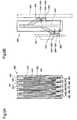
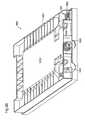
- FIG. 2shows a perspective view of the construction of the ink cartridge pertaining to the embodiment.
- FIGS. 3A-Bshow diagrams of the construction of the board pertaining to the embodiment.
- FIG. 4shows an illustration showing attachment of the ink cartridge in the holder.
- FIG. 5shows an illustration showing the ink cartridge attached to the holder.
- the ink cartridge 100 attached to the holder 4comprises a housing 101 containing ink, a lid 102 providing closure to the opening of the housing 101, a board 200, and a sensor 104.
- an ink supply orifice 110into which the aforementioned ink supply needle 6 inserts when ink cartridge 100 is attached to the holder 4.
- a flared section 103At the upper edge of the front face FR of the housing 101 there is formed a flared section 103.
- a recess 105On the lower side of the center of the front face FR of the housing 101 there is formed a recess 105 bounded by upper and lower ribs 107, 106.
- the aforementioned board 200fits into this recess 105.
- the sensor 104is located in the region posterior to the board 200. The sensor 104 is used to detect remaining ink level, as will be described later.
- FIG. 3Adepicts the arrangement on the surface of the board 200. This surface is the face that is exposed to the outside when the board 200 is mounted on the ink cartridge 100.
- FIG. 3Bdepicts the board 200 viewed from the side.
- a boss slot 201is formed at the upper edge of the board 200
- a boss hole 202is formed at the lower edge of the board 200.
- bosses 108 and 109formed on the lower face of the recess 105 mate with the boss slot 201 and the boss hole 202 respectively.
- the distal ends of the bosses 108 and 109are crushed to effect caulking.
- the board 200is secured within the recess 105 thereby.
- the cover 11is designed to be rotatable about a rotating shaft 9. With the cover 11 rotated upward to the open position, when the ink cartridge 100 is being attached to the holder, the flared section 103 of the ink cartridge is received by a projection 14 of the cover 11. When the cover 11 is closed from this position, the projection 14 rotates downward, and the ink cartridge 100 descends downward (in the Z direction in FIG. 4 ). When the cover 11 is completely closed, a hook 18 of the cover 11 interlocks with a hook 16 of the holder 4. With the cover 11 completely closed, the ink cartridge 100 is secured pressed against the holder 4 by an elastic member 20.
- the ink supply needle 6inserts into the ink supply orifice 110 of the ink cartridge 100, and the ink contained in the ink cartridge 100 is supplied to the printing apparatus 1000 via the ink supply needle 6.
- the ink cartridge 100is attached to the holder 4 by means of inserting it so as to move in the forward direction of the Z axis in FIG. 4 and FIG. 5 .
- the forward direction of the Z axis in FIG. 4 and FIG. 5shall also be referred to as insertion direction of the ink cartridge 100.
- the arrow R in FIG. 3 (a)indicates the insertion direction of the ink cartridge 100 discussed above.
- the board 200comprises a memory 203 disposed on its back face, and a terminal group composed of nine terminals 210 -290 disposed on its front face.
- the memory 203stores information relating to the ink contained in the ink cartridge 100.
- the terminals 210 -290are generally rectangular in shape, and are arranged in two rows generally orthogonal to the insertion direction R. Of the two rows, the row on the insertion direction R side, i.e. the row situated on the lower side in FIG.
- each of the terminals 210 -290contains in its center portion a contact portion CP for contacting a corresponding terminal among the plurality of apparatus-side terminals, described later.
- the terminals 210 -240 forming the upper row and the terminals 250 - 290 forming the lower roware arranged differently from one another, constituting a so-called staggered arrangement, so that the terminal centers do not line up with one another in the insertion direction R.
- the contact portions CP of the terminals 210 -240 forming the upper row and the contact portions CP of the terminals 250 -290 forming the lower roware similarly arranged differently from one another, constituting a so-called staggered arrangement.
- the first sensor drive terminal 250is situated adjacently to two other terminals (the reset terminal 260 and the first short detection terminal 210), and of these, the first short detection terminal 210 for detecting shorting is positioned closest to the first sensor drive-terminal 250.
- the second sensor drive terminal 290is situated adjacently to two other terminals (the second short detection terminal 240 and the data terminal 280), and of these, the second short detection terminal 240 for detecting shorting is positioned closest to the second sensor drive terminal 290.
- the contact portion CP of the first sensor drive terminal 250is situated adjacently to the contact portions CP of two other terminals (the reset terminal 260 and the first short detection terminal 210).
- the contact portion CP of the second sensor drive terminal 290is situated adjacently to the contact portions CP of two other terminals (the second short detection terminal 240 and the data terminal 280).
- the first sensor drive terminal 250 and the second sensor drive terminal 290are situated at the ends of the lower row, i.e. at the outermost positions in the lower row.
- the lower rowis composed of a greater number of terminals than the upper row, and the length of the lower row in the direction orthogonal to the insertion direction R is greater than the length of the upper row, and consequently of all the terminals 210 -290 contained in the upper and lower rows, the first sensor drive terminal 250 and the second sensor drive terminal 290 are situated at the outermost positions viewed in the direction orthogonal to the insertion direction R.
- the contact portion CP of the first sensor drive terminal 250 and the contact portion CP of the second sensor drive terminal 290are respectively situated at the ends of the lower row formed by the contact portions CP of the terminals, i.e., at the outermost positions in the lower row.
- the contact portion CP of the first sensor drive terminal 250 and the contact portion CP of the second sensor drive terminal 290are situated at the outermost positions viewed in the direction orthogonal to the insertion direction R.
- the first short detection terminal 210 and the second short detection terminal 240are respectively situated at the ends of the upper row, i.e., at the outermost positions in the upper row.
- the contact portion CP of the first short detection terminal 210 and the contact portion CP of the second short detection terminal 240are similarly located at the ends of the upper row formed by the contact portions CP of the terminals, i.e. at the outermost positions in the upper row.
- the terminals 220, 230, 260, 270 and 280 connected to the memory 203are situated between the first short detection terminal 210 and the first sensor drive terminal 250, and the second short detection terminal 240 and the second sensor drive terminal 290, located to either side.
- the board 200has width of approximately 12.8 mm in the insertion direction R, width of the approximately 10.1 mm in the direction orthogonal to the insertion direction R, and thickness of approximately 0.71 mm.
- the terminals 210 -290each have width of approximately 1.8 mm in the insertion direction R and width of approximately 1.05 mm in the direction orthogonal to the insertion direction R.
- the dimension values given hereare merely exemplary, with differences on the order of ⁇ 0.5 mm being acceptable, for example.
- the spacing between adjacent terminals in a given row(the lower row or the upper row), for example the interval K between the first short detection terminal 210 and the ground terminal 220, is 1 mm for example.
- the interval J between the upper row and the lower rowis about 0.2 mm.
- differences on the order of ⁇ 0.3 mmare acceptable, for example.
- the terminals 210 -290 of the board 200are electrically connected to a carriage circuit 500 via a contact mechanism 400 disposed on the holder 4.
- the contact mechanism 400shall be described briefly making reference to FIGS. 6A-B .
- FIGS. 6A-Bshow schematics of the construction of the contact mechanism 400.
- the contact mechanism 400has multiple slits 401, 402 of two types that differ in depth, formed in alternating fashion at substantially constant pitch in correspondence with the terminals 210 -290 on the board 200.
- a contact forming member 403, 404endowed with electrical conductivity and resistance.
- the end exposed to the inside of the holderis placed in resilient contact with a corresponding terminal among the terminals 210 -290 on the board 200.
- portions 410 -490which are the portions of the contact forming members 403 and 404 that contact the terminals 210 -290 are shown.
- the portions 410 -490 that contact the terminals 210 -290function as apparatus-side terminals for electrically connecting the printing apparatus 1000 with the terminals 210 -290.
- the portions 410 -490 that contact the terminals 210 -290shall hereinafter be termed apparatus-side terminals 410 -490.
- the apparatus-side terminals 410 -490With the ink cartridge 100 attached to the holder 4, the apparatus-side terminals 410 -490 respectively contact the contact portions CP of the terminals 210 -290 described above ( FIG. 3A ).
- each contact forming member 403 and 404the end lying exposed on the exterior of the holder 4 is placed in resilient contact with a corresponding terminal among the terminals 510 -590 furnished to the carriage circuit 500.
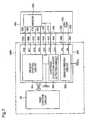
- FIG. 7shows a brief diagram of the electrical arrangement of the ink cartridge and the printing apparatus.
- FIG. 8shows a brief diagram of the electrical arrangement, focusing on the cartridge detection/short detection circuit.
- the ground terminal 220, the power supply terminal 230, the reset terminal 260, the clock terminal 270 and the data terminal 280are electrically connected to the memory 203.
- the memory 203is, for example, EEPROM comprising serially accessed memory cells, and performing data read/write operations in sync with a clock signal.
- the ground terminal 220is grounded via a terminal 520 on the printing apparatus 1000 side.
- the reset terminal 260is electrically connected to a terminal 560 of the carriage circuit 500, and is used to supply a reset signal RST to the memory 203 from the carriage circuit 500.
- the clock terminal 270is electrically connected to a terminal 570 of the carriage circuit 500, and is used to supply the clock signal CLK to the memory 203 from the carriage circuit 500.
- the data terminal 280is electrically connected to a terminal 580 of the carriage circuit 500, and is used for exchange of data signals SDA between the carriage circuit 500 and the memory 203.
- first short detection terminal 210the second short detection terminal 240, or both are electrically connected with the ground terminal 220.
- first short detection terminal 220is electrically connected to the ground terminal 220.
- the first short detection terminal 210 and the second short detection terminal 240are electrically connected respectively to the terminals 510, 540 of the carriage circuit 500, and used for cartridge detection and short detection, described later.
- a piezoelectric elementis used as the sensor 104.
- the remaining ink levelcan be detected by applying driving voltage to the piezoelectric element to induce the piezoelectric element to vibrate through the inverse piezoelectric effect, and measuring the vibration frequency of the voltage produced by the piezoelectric effect of the residual vibration.
- this vibration frequencyrepresents the characteristic frequency of the surrounding structures (.e.g. the housing 101 and ink) that vibrate together with the piezoelectric element.
- the characteristic frequencychanges depending on the amount of ink remaining within the ink cartridge, so the remaining ink level can be detected by measuring this vibration frequency.
- the second sensor drive terminal 290is electrically connected to one electrode of the piezoelectric element used as the sensor 104, and the first sensor drive terminal 250 is electrically connected to the other electrode. These terminals 250, 290 are used for exchange of sensor driving voltage and output signals from the sensor 104, between the carriage circuit 500 and the sensor 104.
- the carriage circuit 500comprises a memory control circuit 501, a cartridge detection/short detection circuit 502, and a sensor driving circuit 503.
- the memory control circuit 501is a circuit connected to the terminals 530, 560, 570, 580 of the carriage circuit 500 mentioned above, and used to control the memory 203 of the ink cartridge 100 to perform data read/write operations.
- the memory control circuit 501 and the memory 203are low-voltage circuits driven at relatively low voltage (in the embodiment, a maximum of about 3.3 V).
- the memory control circuit 501can employ a known design, and as such need not be described in detail here.
- the sensor driving circuit 503is a circuit connected to the terminals 590 and 550 of the carriage circuit 500, and used to control the driving voltage output from these terminals 590 and 550 to drive the sensor 104, causing the sensor 104 to detect the remaining ink level.
- the driving voltagehas a generally trapezoidal shape, and contains relatively high voltage (in the embodiment, about 36 V).
- the sensor driving circuit 503 and the sensor 104are high-voltage circuits using relatively high voltage via the terminals 590 and 550.
- the sensor driving circuit 503is composed of a logic circuit for example, but need not be described in detail herein.
- the cartridge detection/short detection circuit 502is a low-voltage circuit driven using relatively low voltage (in the embodiment, a maximum of about 3.3V). As depicted in FIG. 8 , the cartridge detection/short detection circuit 502 comprises a first detection circuit 5021 and a second detection circuit 5022. The first detection circuit 5021 is connected to the terminal 510 of the carriage circuit 500. The first detection circuit 5021 has a cartridge detection function for detecting whether there is contact between the terminal 510 and the first short detection terminal 210 of the board 200, and a short detection function for detecting shorting of the terminal 510 to the terminals 550 and 590 which output high voltage.
- the first detection circuit 5021has a reference voltage V_ref1 applied to one end of two series-connected resistors R2, R3, with the other end being grounded, thereby maintaining the potential at point P1 and P2 in FIG. 4 at V_ref1 and V_ref2, respectively.
- V_ref1shall be termed the short detection voltage
- V_ref2shall be termed the cartridge detection voltage.
- the short detection voltage V_ref1is set to 6.5 V
- the cartridge detection voltage V_ref2is set to 2.5 V.
- the short detection voltage V_ref1(6.5 V) is input to the negative input pin of a first Op-Amp OP1
- the cartridge detection voltage V_ref2(2.5 V) is input to the negative input pin of a second Op-Amp OP2.
- the potential of the terminal 510is input to the positive input pins of the first Op-Amp OP1 and the second Op-Amp OP2.
- These two Op-Ampsfunction as a comparator, outputting a High signal when the potential input to the negative input pin is higher than the potential input to the positive input pin, and conversely outputting a Low signal when the potential input to the negative input pin is lower than the potential input to the positive input pin.
- the terminal 510is connected to a 3.3 V power supply VDD 3.3 via a transistor TR1.
- the potential of the terminal 510will be set at about 3 V.
- the terminal 510comes into contact with the first short detection terminal 210 of the board 200 described previously.
- a short detection enable signal ENis input from the main control circuit 40 to the other input pin of the AND circuit AA.
- the first detection circuit 5021outputs the High signal from the Op-Amp OP1 as a short detection signal AB1. That is, execution of the short detection function of the first detection circuit 5021 is controlled by means of the short detection enable signal EN of the main control circuit 40.
- the short detection signal AB1 from the AND circuit AAis output to the main control circuit 40, as well as being output to the base pin of the transistor TR1 via resistance R1.
- the transistor TR1it is possible to prevent high voltage from being applied to the power supply VDD 3.3 via the terminal 510 when a short is detected (when the short detection signal AB1 is HI).
- the second detection circuit 5022has a cartridge detection function for detecting whether there is contact between the terminal 540 and the second short detection terminal 240 of the board 200, and a short detection function for detecting shorting of the terminal 540 to the terminals 550 and 590 which output high voltage. Since the second detection circuit 5022 has the same arrangement as the first detection circuit 5021, a detailed illustration and description need not be provided here.
- the cartridge detection signal output by the second detection circuit 5022shall be denoted as CS2, and the short detection signal as AB2.
- the carriage circuit 500corresponding to a single ink cartridge 100 has been described above.
- four of the cartridge detection/short detection circuits 502 described abovewill be provided, at each of the attachment locations for the four ink cartridges 100.
- a single sensor driving circuit 503is provided, and a single sensor driving circuit 503 is connectable to each of the sensors 104 of the ink cartridges 100 attached at the four attachment locations by means of a switch(not shown).
- the memory control circuit 501is a single circuit responsible for processes relating to the four ink cartridges.
- the main control circuit 40is a computer of known design comprising a central processing unit (CPU), a read-only memory (ROM), and a random access memory (RAM). As noted, the main control circuit 40 controls the entire printer; in FIG. 8 , however, only those elements necessary for description of the embodiment are selectively illustrated, and the following description refers to the illustrated arrangement.
- the main control circuit 40comprises a cartridge determining module M50 and a remaining ink level determining module M60. On the basis of the received cartridge detection signals CS1, CS2, the cartridge determining module M50 executes a cartridge determination process, described later.
- the remaining ink level determining module M60controls the sensor driving circuit 503, and executes a remaining ink level detection process, described later.
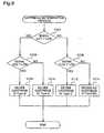
- FIG. 9shows a flowchart depicting the processing routine of the cartridge determination process.
- FIGS. 10A-Cshow illustrations depicting three types of terminal lines on the board 200.
- the board 200Before turning to the cartridge determination process, the board 200 will be described further with reference to FIG. 10 .
- the board 200 mentioned previouslycomes in three types, depending on the wiring pattern of the first short detection terminal 210, the second short detection terminal 240, and the ground terminal 220. These three types are designated respectively as Type A, Type B, and Type C.
- the Type A board 200is arranged with the first short detection terminal 210 and the ground terminal 220 electrically connected by a conducting line 207, while the second short detection terminal 240 and the ground terminal 220 are not electrically connected.
- FIG. 10Athe Type A board 200 is arranged with the first short detection terminal 210 and the ground terminal 220 electrically connected by a conducting line 207, while the second short detection terminal 240 and the ground terminal 220 are not electrically connected.
- the Type B board 200is arranged with both the first short detection terminal 210 and the second short detection terminal 240 electrically connected with the ground terminal 220 by a conducting line 207.
- the Type C board 200is arranged with the second short detection terminal 240 and the ground terminal 220 electrically connected by a conducting line 207, while the first short detection terminal 210 and the ground terminal 220 are not electrically connected.
- a board 200 of predetermined type, selected with reference to ink type or ink quantity for example,is disposed on the ink cartridge 100.
- a Type A board 200could be disposed on an L size cartridge containing a large quantity of ink; a Type B board 200 could be disposed on an M size cartridge containing a standard quantity of ink; and a Type C board 200 could be disposed on an S size cartridge containing a small quantity of ink.
- the cartridge determining module M50 of the main control circuit 40constantly receives from the cartridge detection/short detection circuit 502 the cartridge detection signals CS1, CS2 for each of the four attachment locations of the holder 4, and using these signals executes the cartridge determination process for each of the attachment locations.
- the cartridge determining module M50When the cartridge determining module M50 initiates the cartridge determination process for a selected attachment location, the cartridge determining module M50 first ascertains whether the cartridge detection signal CS1 from the cartridge detection/short detection circuit 502 in the selected attachment location is a Low signal (Step S102). Next, the cartridge determining module M50 ascertains whether the cartridge detection signal CS2 in the selected attachment location is a Low signal (Step S104 or S106). If as a result the cartridge detection signals CS1 and CS2 are both Low signals (Step S102: YES and Step S104: YES), the cartridge determining module M50 decides that the ink cartridge 100 attached to the selected attachment location is furnished with the Type B board 200 (Step S108).
- the cartridge determining module M50in the event that the cartridge detection signal CS1 is a Low signal and the cartridge detection signal CS2 is a High signal (Step S102: YES and Step S104: NO), decides that the ink cartridge is furnished with the Type A board 200 (Step S110); or in the event that the cartridge detection signal CS1 is a High signal and the cartridge detection signal CS2 is a Low signal (Step S102: NO and Step S104: YES), decides that the ink cartridge is furnished with the Type C board 200 described above (Step S112).
- Step S102NO and Step S104: NO
- the cartridge determining module M50decides that no cartridge is attached to the selected attachment location (Step S114). In this way, the cartridge determining module M50 determines whether an ink cartridge 100 is attached, and if so what type, for each of the four attachment locations.
- FIG. 11shows a flowchart depicting the processing routine of the remaining ink level detection process.
- FIGS. 12A-Cshow timing charts depicting temporal change in the shorting-detection enable signal and sensor voltage during execution of the remaining ink level detection process;
- the remaining ink level determining module M60 of the main control circuit 40in the event that the remaining ink level in the ink cartridge 100 attached at any of the attachment locations of the holder 4 is to be detected, first sets to High the short detection enable signal EN to all of the cartridge detection/short detection circuits 502 (Step S202).
- the short detection functionis enabled in all of the cartridge detection/short detection circuits 502, and if voltage above the reference voltage V_ref1 (6.5 V) is applied to the aforementioned terminal 520 and terminal 540, are able to output High signals as the short detection signals AB1, AB2.
- a state in which the short detection enable signal EN are High signalsis a state in which shorting of the terminal 510 or terminal 540 to the terminal 550 or terminal 590 is monitored.
- the remaining ink level determining module M60instructs the sensor driving circuit 503 to output driving voltage from the terminal 550 or terminal 590 to the sensor 104, and detect the remaining ink level output (Step S204).
- the sensor driving circuit 503receives an instruction signal from the remaining ink level determining module M60
- the sensor driving circuit 503outputs driving voltage from either the terminal 550 or the terminal 590, the voltage being applied to the piezoelectric element which constitutes the sensor 104 of the ink cartridge 100, charging the piezoelectric element and causing it to distort by means of the inverse piezoelectric effect.
- the sensor driving circuit 503subsequently drops the applied voltage, whereupon the charge built up in the piezoelectric element is discharged, causing the piezoelectric element to vibrate.
- the driving voltageis the voltage shown during time interval T1.
- the driving voltagefluctuates between the reference voltage and the maximum voltage Vs in such a way as to describe a trapezoidal shape.
- the maximum voltage Vsis set to relatively high voltage (e.g. about 36 V).
- the sensor driving circuit 503detects the voltage produced by the piezoelectric effect as a result of vibration of the piezoelectric element (in FIG.
- this vibration frequencyrepresents the characteristic frequency of the surrounding structures (the housing 101 and ink) that vibrate together with the piezoelectric element, and changes depending on the amount of ink remaining within the ink cartridge 100, so the remaining ink level can be detected by measuring this vibration frequency.
- the sensor driving circuit 503outputs the detected result to the remaining ink level determining module M60 of the main control circuit 40.
- the remaining ink level determining module M60When the remaining ink level determining module M60 receives the detected result from the sensor driving circuit 503, the remaining ink level determining module M60 brings the short detection enable signal EN, which was previously set to a High signal in Step S202, back to a Low signal (Step S206), and terminates the process.
- the interval that the remaining ink level is being detectedis a state in which the short detection enable signal EN is set to a High signal to enable short detection. In other words, remaining ink level is detected while the occurrence of shorting is being monitored by the cartridge detection/short detection circuit 502.
- Step S204The process carried out in the event that, during execution of detection of the remaining ink level (Step S204), the remaining ink level determining module M60 receives a High signal as the short detection signal AB1 or AB2, e.g. shorting is detected shall be described here.
- FIG. 11a flowchart of the interrupt processing routine when shorting is detected is shown as well.
- the short detection enable signal ENis currently set to High, at the instant that the sensor driving voltage goes above the short detection voltage V_ref1 (6.5 V), a High signal will be output as the short detection signals AB1, AB2 from the cartridge detection/short detection circuit 502.
- the remaining ink level determining module M60receives either of these short detection signals AB1, AB2, the remaining ink level determining module M60 suspends detection of remaining ink level, and executes the interrupt processing when shorting is detected.
- the remaining ink level determining module M60immediately instructs the sensor driving circuit 503 to suspend the output of sensor driving voltage (Step S208).
- the remaining ink level determining module M60without carrying out remaining ink level detection process to its conclusion, brings the short detection enable signal EN back to a Low signal (Step S206) to terminate the process.
- the main control circuit 40may take some countermeasure, such as notifying the user of the shorting.
- FIG. 12Adepicts change of the detection enable signal EN through time.
- FIG. 12Bdepicts sensor voltage in the event that neither the terminal 510 nor the terminal 540 is shorting to the terminal that outputs the sensor driving voltage of the terminals 550 and 590, so that the remaining ink level detection process is being executed normally.
- FIG. 12Cdepicts sensor voltage in the event that the terminal 510 or the terminal 540 is shorting to the terminal that, of the terminals 550 and 590, outputs the sensor driving voltage.
- the detection enable signal ENis a High signal.
- Vsis set at 36 V.
- the sensor voltagedrops at the instant that it goes above the short detection voltage V_ref1 (6.5 V). This is due to the fact that, at the instant that the sensor voltage goes above the short detection voltage V_ref1 (6.5 V), a High signal is output as the short detection signal AB1 or AB2 from the cartridge detection/short detection circuit 502 to the remaining ink level determining module M60, and the remaining ink level determining module M60 receiving this signal immediately drops the sensor driving voltage.
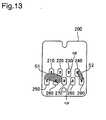
- FIG. 13shows an illustration of a scenario of shorting.
- the likely scenario for shorting to other terminals by the terminals 550 and 590 which output the sensor driving voltageis, for example, the case depicted in FIG. 13 , in which an electrically conductive ink drop S1 or a water drop S2 formed by condensation has become deposited on the board 200 of the ink cartridge 100, bridging the gap between the first sensor drive terminal 250 or the second sensor drive terminal 290 and another terminal or terminals on the board 200, producing shorting.
- ink drop S1 that has adhered to the surface of the carriage 3 or ink supply needle 6disperses and adheres as shown in FIG. 13 by the motion of attaching or detaching of ink cartridge 100.
- the terminal 550 that outputs the sensor driving voltagewhen the ink cartridge 100 is attached, the terminal 550 that outputs the sensor driving voltage, for example, will short to another terminal 510, 520, or 560 of the carriage circuit 500 via the first sensor drive terminal 250 and the terminals ( FIG. 13 : terminals 210, 220, 260) bridged by the ink drop S1 to the sensor drive terminal 250.
- the terminal 590 that outputs the sensor driving voltagewill short to another terminal 540 of the carriage circuit 500 via the second sensor drive terminal 290 and the second short detection terminal 240 ( FIG. 13 ) bridged by the water drop S2 to the second sensor drive terminal 290, for example.
- Such a shortingis caused by various factor as well as the adhesion of the ink drop.
- the shortingmay be caused by trapping electrically conducting object, for example, paper clip on carriage 3.
- the shortingalso may be caused by adhesion to terminals of the electrically conducting material, for example, skin oil of user.
- the first sensor drive terminal 250 and the second sensor drive terminal 290 which apply the driving voltage to the sensorare arranged at the two ends of the terminal group, so the number of adjacent terminals is small. As a result, the likelihood of the first sensor drive terminal 250 and the second sensor drive terminal 290 shorting to other terminals is low.
- the shortingwill be detected by the aforementioned cartridge detection/short detection circuit 502. For example, shorting of the first sensor drive terminal 250 to another terminal caused by the ink drop S1 infiltrating from the first sensor drive terminal 250 side will be detected instantly and the output of sensor driving voltage will be suspend, preventing or reducing damage to the memory 203 and the printing apparatus 1000 circuits (the memory control circuit 501 and the cartridge detection/short detection circuit 502) caused by the shorting.
- the first short detection terminal 210is adjacent to the first sensor drive terminal 250 and situated closest to the first sensor drive terminal 250. Consequently, in the event that the first sensor drive terminal 250 should short to another terminal or terminals due to the ink drop S1 or the water drop S2, there is a high likelihood that the first sensor drive terminal 250 will short to the first short detection terminal 210 as well. Consequently, shorting of the first sensor drive terminal 250 to another terminal can be detected more reliably.
- the first short detection terminal 210is also used by the cartridge detection/short detection circuit 502 to determine whether an ink cartridge 100 is attached, as well as to determine the type of attached ink cartridge 100.
- the number of terminals on the board 200can be kept down, and it becomes possible to reduce the number of board 200 manufacturing steps and the number of parts for the board 200.
- the second short detection terminal 240is the terminal situated closest to the second sensor drive terminal 290.
- the first sensor drive terminal 250 and the first short detection terminal 210 on the one hand, and the second sensor drive terminal 290 and the second short detection terminal 240 on the other,are situated at the ends of the terminal group so that the other terminals (220, 230, 260 -270) lie between them. Consequently, if foreign matter (the ink drop S1, water drop S2 etc.) should infiltrate from either side as indicated by the arrows in FIG. 13 , this infiltration can be detected before it infiltrates as far as the other terminals (220, 230, 260 - 270). Consequently, damage to the circuits of the memory 203 and the printing apparatus 1000 due to infiltration of foreign matter can be prevented or reduced.
- foreign matterthe ink drop S1, water drop S2 etc.
- the first sensor drive terminal 250 and the second sensor drive terminal 290are arranged in the row on the insertion direction R side (lower row).
- the terminals 250, 290 to which sensor driving voltage including high voltage is appliedare situated to the back in the insertion direction, there is less likelihood that ink drops or foreign matter (e.g. a paperclip) will infiltrate to the location of these terminals 250, 290.
- damage to the circuits of the memory 203 and the printing apparatus 1000 caused by infiltration of foreign mattercan be prevented or reduced.
- the terminal group of the board 200is arranged in a staggered pattern. As a result, unwanted contact of the terminals of the ink cartridge 100 with the terminals of the printing apparatus 1000 (the contact forming members 403, 404 mentioned previously) during the attachment operation can be prevented or reduced.
- FIGS. 14A -16Bshow first diagrams depicting boards pertaining to variations.
- FIGS. 15A-Cshow second diagrams depicting boards pertaining to variations.
- FIGS. 16A-Bshow third diagrams depicting boards pertaining to variations.
- the first short detection terminal 210is similar to the first short detection terminal 210 of the board 200 of the embodiment, but has at its lower end an extended portion that reaches into proximity with the lower edge of the lower row.
- the extended portionis positioned between the first sensor drive terminal 250 and the reset terminal 260 of the lower row.
- the first sensor drive terminal 250 and terminal other than the first short detection terminal 210are shorting, there is a high possibility that the first sensor drive terminal 250 and the first short detection terminal 210 are shorting and the sensor driving voltage is suspended. Accordingly, problems caused by shorting of the first sensor drive terminal 250 to another terminal (in the example of FIG. 14A , the reset terminal 260) can be prevented or reduced.
- the second short detection terminal 240 of the board 200bis also similar in shape to the first short detection terminal 210 mentioned above, and shorting of the second sensor drive terminal 290 to another terminal will also be detected more reliably.
- the board 200c depicted in FIG. 14Bhas, in addition to the arrangement of the board 200b described above, also has an extended portion located at the upper side of the first sensor drive terminal 250, and reaching into proximity with the upper edge of the upper row.
- an ink drop S4as depicted in FIG. 14 (b)
- shorting of the short detection terminal 210 to the extended portion of the first sensor drive terminal 250will be detected.
- the first sensor drive terminal 250 and terminal other than the first short detection terminal 210are shorting, there is a high possibility that the first sensor drive terminal 250 and the first short detection terminal 210 are shorting and the sensor driving voltage is suspended. Accordingly, problems caused by shorting of the first sensor drive terminal 250 to another terminal can be prevented or reduced.
- the second sensor drive terminal 290 of the board 200cis also similar in shape to the first sensor drive terminal 250 mentioned above, and infiltration of an ink drop from the end, at the end at which the second sensor drive terminal 290 is situated, can be detected instantly.
- the board 200d depicted in FIG. 14Cdiffers from the board 200 of the embodiment in that there is no second short detection terminal 240.
- the second short detection terminal 240does not carry out detection of contact by means of the cartridge detection/short detection circuit 502 (since there is no shorting to the ground terminal 220). Consequently, in the case of the Type A board 200, the second short detection terminal 240 is used for short detection only and accordingly can be dispensed with.
- the first short detection terminal 210is at the location closest to the first sensor drive terminal 250, when the first sensor drive terminal 250 and terminal other than the first short detection terminal 210 are shorting, there is a high possibility that the first sensor drive terminal 250 and the first short detection terminal 210 are shorting and the sensor driving voltage is suspended. Infiltration of an ink drop to second sensor drive terminal 290 side will also be detected to a certain extent.
- the symbol CPrepresents the location of contact with the contact forming member 403 that would contact the second short detection terminal 240 if the second short detection terminal 240 were present (i.e. the contact forming member 403 corresponding to the terminal 540 of the carriage circuit 500).
- the second short detection terminal 240Even in the case that the second short detection terminal 240 is absent, if a shorting should occur between the second sensor drive terminal 290 and the contact forming member 403 corresponding to the terminal 540 of the carriage circuit 500 due to an ink drop S5, infiltration of the ink drop S5 will be detected. Similarly, in the case of a Type C board 200, the first short detection terminal 210 may be dispensed with.
- the first sensor drive terminal 250 and the first short detection terminal 210have elongated shape reaching from the vicinity of the upper edge of the upper row to the vicinity of the lower edge of the lower row.
- the terminals of this shapecan contact the corresponding contact forming portions 403 arranged in a staggered pattern.
- first short detection terminal 210is located between first sensor drive terminal 250 and terminal other than the first short detection terminal 210. Accordingly, when the first sensor drive terminal 250 and terminal other than the first short detection terminal 210 are shorting, there is a high possibility that the first sensor drive terminal 250 and the first short detection terminal 210 are shorting and the sensor driving voltage is suspended.
- the second sensor drive terminal 290 and the second short detection terminal 240 of the board 200ehave shape similar to the first sensor drive terminal 250 and the first short detection terminal 210 described above. Accordingly, when the second sensor drive terminal 290 and terminal other than the second short detection terminal 240 are shorting, there is a high possibility that the second sensor drive terminal 290 and the second short detection terminal 240 are shorting. As a result, the possibility preventing or reducing the problems caused by shorting of the sensor drive terminal 250, 290 to another terminal becomes higher.
- the terminal which corresponds to the first short detection terminal 210 and the ground terminal 220 in the board 200 pertaining to the embodimentis an integral terminal 215 wherein these two terminals are integrally formed as a single member.
- This board 200fcan be used in place of the Type A or Type B board 200 ( FIG. 10 ) whose first short detection terminal 210 and ground terminal 220 are shorted. With the board 200f, the need is obviated for a line between the first short detection terminal 210 and the ground terminal 220, which was required in the case of in the board 200 pertaining to the embodiment, so the board 200 requires fewer process steps and fewer parts.
- the terminals 210 -240 of the upper roweach have shape similar to the first short detection terminal 210 of the board 200b described previously. Specifically, each of the terminals 210 -240 has an extended portion situated at the lower edge of the corresponding terminal of the board 200 pertaining to the embodiment and reaching into proximity with the lower edge of the lower row.
- the terminals 250 -290 of the lower row of the board 200gare similar in shape to the first sensor drive terminal 250 of the board 200c described earlier. Specifically, the each of the terminals 250 -290 has an extended portion situated at the upper edge of the corresponding terminal of the board 200 pertaining to the embodiment and reaching into proximity with the upper edge of the upper row.
- the terminals 210 -290 of the board 200gare arranged so as to form a terminal group composed of a single row of terminals of generally oar shape of in mutually different arrangement, rather than being arranged in two rows.
- the first sensor drive terminal 250 and the second sensor drive terminal 290 to which the high-voltage sensor driving voltage is appliedare positioned at the two ends of the single row of the terminal group, with the first short detection terminal 210 and the second short detection terminal 240 respectively arranged adjacently inward from the first sensor drive terminal 250 and the second sensor drive terminal 290.
- an ink drop or foreign matter infiltrating from either endcan be detected immediately at the point in time that shorting occurs between the first sensor drive terminal 250 and the short detection terminal 210, or between the second sensor drive terminal 290 and the second short detection terminal 240.
- the first sensor drive terminal 250 or the second sensor drive terminal 290should short to another terminal, in the case where the shorting is due to an ink drop or the like, the likelihood is extremely high that shorting between the first sensor drive terminal 250 and the short detection terminal 210, or between the second sensor drive terminal 290 and the second short detection terminal 240, will occur at the same time. Consequently, shorting of the first sensor drive terminal 250 or the second sensor drive terminal 290 to another terminal can be detected reliably. As a result, damage to the memory 203 and the printing apparatus 1000 circuits (the memory control circuit 501 and the cartridge detection/short detection circuit 502) caused by the shorting can be prevented or minimized.
- the terminals 210 -290have elongated shape extending over a distance equivalent to two rows of the board 200 pertaining to the embodiment, in a manner similar to the first sensor drive terminal 250 and the first short detection terminal 210 of the board 200e described previously.
- the terminals of this shapeas the contact locations are indicated by the symbol cp in FIG. 15C , can contact the corresponding contact forming portions 403 arranged in a staggered pattern.
- the terminals 210 -290are arranged so as to form a single row in the orthogonal direction to the insertion direction R, in a manner similar to the board 200g described above. Also, like the board 200g, the first sensor drive terminal 250 and the second sensor drive terminal 290 to which the high-voltage sensor driving voltage is applied are positioned at the two ends of the single row of terminals, with the first short detection terminal 210 and the second short detection terminal 240 respectively arranged adjacently inward from the first sensor drive terminal 250 and the second sensor drive terminal 290. As a result, the board 200h affords advantages analogous to those of the board 200g described above.
- the first short detection terminal 210 of the board 200i depicted in FIG. 16Ahas a shape that is longer on the left side in the drawing, as compared to the first short detection terminal 210 of the board 200 pertaining to the embodiment. Additionally, the first short detection terminal 210 of the board 200i has an extended portion reaching from the left edge portion to the vicinity of the lower edge of the lower row. The extended portion is situated to the left of the first sensor drive terminal 250 in the lower row. In other words, the extended portion is disposed to further from the middle of the terminal group in a direction substantially orthogonal to the insertion direction R than the first sensor drive terminal 250.
- the first short detection terminal 210is situated outwardly (to the left side) of the first sensor drive terminal 250, when viewed in terms of the contact portion CP of the terminal, of the contact portions CP of all of the terminals 210 -290 the contact portion CP of the first sensor drive terminal 250 is the one situated at the outermost position (left side), in the same manner as in the embodiment. Also, shorting between the first sensor drive terminal 250 and the first short detection terminal 210 that includes the contact portion CP adjacent to the contact portion CP of the first sensor drive terminal 250 is detected. Accordingly, the board 200i pertaining to this variation affords advantages similar to the board 200 pertaining to the embodiment.
- the length of a first portion that is a portion adjacent to the circumferential edge of the first short detection terminal 210 among the circumferential edge of the first sensor drive terminal 250becomes long. As shown in FIG. 16B , the length of the first portion is longer than that of a second portion that is a portion adjacent to the circumferential edge of the reset terminal 260 among the among the circumferential edge of the first sensor drive terminal 250.
- the reset terminal 260are shorting, there is a high possibility that the first sensor drive terminal 250 and the first short detection terminal 210 are shorting. Accordingly, the sensor driving voltage is suspended and problems caused by shorting of the first sensor drive terminal 250 to another terminal can be prevented or reduced with higher probability.
- the first short detection terminal 210 of the board 200p in FIG. 16Chas the longer extended portion than the first short detection terminal 210 of the board 200i.
- the extended portion of the first short detection terminal 210 of the board 200pextends from upper left to lower right of the first sensor drive terminal 250 along the circumferential edge of the first sensor drive terminal 250.
- the length of the first portion in the board 200pis longer than that in the board 200i. Accordingly, when the first sensor drive terminal 250 and terminal other than the first short detection terminal 210 are shorting, there is a higher possibility the sensor driving voltage is suspended and problems caused by shorting of the first sensor drive terminal 250 to another terminal can be prevented or reduced.
- the first short detection terminal 210 of the board 200q in FIG. 16Dhas the longer extended portion than the first short detection terminal 210 of the board 200i and 200p.
- the extended portion of the first short detection terminal 210 of the board 200qextends from upper left through lower to upper right of the first sensor drive terminal 250 along the circumferential edge of the first sensor drive terminal 250.
- the first short detection terminal 210is formed so as to surround the first sensor drive terminal 250 completely.
- the length of the first portion in the board 200qis longer than that in the board 200i and 200p. Accordingly, when the first sensor drive terminal 250 and terminal other than the first short detection terminal 210 are shorting, there is a higher possibility the sensor driving voltage is suspended and problems caused by shorting of the first sensor drive terminal 250 to another terminal can be prevented or reduced.
- board 200i, 200p, 200qare added the direction in which the portion of the first short detection terminal 210 is located adjacently to a portion of the sensor drive terminal 250 by providing the extended portion of the first short detection terminal 210.
- the extended potion of the first short detection terminal 210located adjacently to left border of the first sensor drive terminal 250 in a lateral direction towards an edge of the ink cartridge 100, and the first short detection terminal 210 itself is located adjacently to upper border of the first sensor drive terminal 250 in opposite direction of the insertion direction R.
- the extended potion of the first short detection terminal 210is located adjacently to lower border of the first sensor drive terminal 250 in the insertion direction R. Furthermore, about board 200q, the extended potion of the first short detection terminal 210 is located adjacently to right border of the first sensor drive terminal 250 in lateral direction away from an edge of the ink cartridge 100. In other words, about board 200q, at least a potion of the first short detection terminal 210 is located adjacently to the first sensor drive terminal 250 in all direction.
- the extended portion of the first short detection terminal 210adds the direction in which the first short detection terminal 210 and the first sensor drive terminal 250 are adjacent each other, and prevents or reduces problems caused by shorting of the first sensor drive terminal 250 to another terminal with much high probability.
- the boards 200i, 200p, 200q pertaining to this variationonly the first short detection terminal 210 on the left side is furnished with a structure having the extended portion described above, but it would be possible to furnish the second short detection terminal 240 on the right side with a structure having an extended portion, in addition to the first short detection terminal 210 or instead of the first short detection terminal 210. In this case as well, there are afforded advantages analogous to those of the boards 200i, 200p, 200q pertaining to this variation.
- the board 200j depicted in FIG. 16Bhas an integral terminal 215 wherein the first short detection terminal 210 and the ground terminal 220 in the board 200 pertaining to the embodiment are integrally formed as a single member.
- the integral terminal 215 of the board 200jdiffers in shape from the integral terminal 215 of the board 200f described previously.
- the integral terminal 215 of the board 200jlike the first short detection terminal 210 of the board 200i described in Variation 8, has a shape elongated on the left side, and has an extended portion reaching from the left edge portion to the vicinity of the lower edge of the lower row. In this case, advantages analogous to those of the board 200i pertaining to Variation 8 are attained, while reducing the number of production steps and parts needed for the board.
- FIGS. 17A -18Dshow diagrams depicting the construction around boards of ink cartridges pertaining to variations.
- FIGS. 18A-Dshow cross sections A-A to D-D in FIG. 17 .
- the board 200k depicted in FIG. 17Ais furnished with seven terminals 210 - 240 and 260 -280, out of the nine terminals 210 -290 furnished to the board 200 of the embodiment. Out of the nine terminals 210 -290 furnished to the board 200 of the embodiment, the board 200k lacks the first sensor drive terminal 250 and the second sensor drive terminal 290.
- the board 200k pertaining to this variationis furnished with notches NT1 or NT2 situated in zones that include the locations where the first sensor drive terminal 250 and the second sensor drive terminal 290 were disposed on the board 200 pertaining to the embodiment.
- the notchesmay have the shape indicated by the solid lines NT1, or the shape indicated by the broken lines NT2, in FIG. 17A .
- Terminals 150 and 190having function similar to the first sensor drive terminal 250 and the second sensor drive terminal 290 of the board 200 in the embodiment are arranged on the housing 101 situated to the rear of the board 200k. Naturally, with the ink cartridge 100 attached to the holder 4, these terminals 150 and 190 are situated at locations contacting the corresponding apparatus-side terminals 450 and 490.
- FIG. 18AA-A cross section viewed in FIG. 17A is depicted in FIG. 18A .
- a depressed portion DEformed by a gap between the notch NT1 of the board 200k and the terminal 150, is situated between the terminal 150 and the adjacent terminals 260, 210 (in FIG. 18A , the reset terminal 260 is shown). While omitted from the drawing, a similar depressed portion DE is situated between the terminal 190 and the adjacent terminals 280, 240.
- the board 200m depicted in FIG. 17Bis instead furnished with through-holes HL situated at locations corresponding to the locations where the first sensor drive terminal 250 and the second sensor drive terminal 290 are situated on the board 200 pertaining to the embodiment.
- B-B cross section viewed in FIG. 17Bis depicted in FIG. 18B .
- Other arrangements of the ink cartridge 100 pertaining to Variation 11are the same as those of the ink cartridge 100 pertaining to Variation 10.
- depressed portions DEare situated between the terminals 150, 190 and the adjacent terminals. Accordingly, the ink cartridge 100 pertaining to this variation affords advantages analogous to those of the ink cartridge 100 pertaining to Variation 10.
- FIGS. 19A-Dshow fourth diagrams depicting boards pertaining to variations.
- the board 200rincludes the upper row formed by four terminals and the lower row formed by five terminals, as with the board 200 pertaining to the embodiment. Arrangement and function of the terminals 210 - 290 forming the upper row and the lower row of board 200r is the same as those of the terminals of board 200 in the embodiment, so the detailed description thereof is omitted.
- the board 200r shown in FIG. 19Ahas the dummy terminals DT between the upper row and the lower row and on the underside (the insertion direction side) of the lower row.
- the dummy terminals DTfor example, are made of the same material as other terminal 210-290.
- FIG. 19Cshows E-E cross-section including dummy terminals DT.
- the dummy terminals DThas about the same thickness as other terminal 210-290.
- the dummy terminals DTare for scraping away foreign object adherent on the contact forming members 403, for example, dust when ink cartridge 100 is attached or detached. This enables to prevent foreign object from being brought to the terminal to be contacted by contact forming member 403 (for example, the first sensor drive terminal 250 in FIG. 19C ) when ink cartridge 100 is attached or detached, and to prevent contact failure between the terminal and the contact forming member 403.
- the board 200r shown in FIG. 19Ahas the dummy terminal DT between the first sensor drive terminal 250 and the short detection terminal 210, so you can't say first sensor drive terminal 250 is located adjacent to first short detection terminal 210.
- the dummy terminals DTis not connected to memory 203 and not connected to the apparatus-side terminals 510-590 on printing apparatus 1000. Therefore, the shorting between the first sensor drive terminal 250 and the dummy terminals DT never cause any problem. Accordingly, the board 200r can afford working effects analogous to the board 200 pertaining to the embodiment.
- first sensor drive terminal 250is not located adjacent to first short detection terminal 210 in a precise sense, at least a portion of the first short detection terminal 210 is arranged relative to at least a portion of the first sensor drive terminal 250, without a terminal connected to memory 203 (terminal 220, 230, 260-280) therebetween in at least one direction, for the detection of shorting between the first sensor drive terminal 250 and the first short detection terminal 210.
- the first sensor drive terminal 250is substantially located adjacent to first short detection terminal 210.
- the output of sensor driving voltageis suspend and damage to the circuits of the memory 203 and the printing apparatus 1000 caused by shorting can be prevented or reduced.
- FIG. 2shows a perspective view of the construction of the ink cartridge pertaining to the variation 13.
- FIG 21shows a picture of the ink cartridge pertaining to the variation 13 being attached to the printer.
- Ink cartridge 100b pertaining to Variation 13is configured for installation in an "off carriage" type printer, i.e., one in which the ink cartridge is not installed on a carriage.
- Off carriage type printersare typically large-scale printers; the ink cartridges employed in such large-scale printers are typically larger in size than the ink cartridges employed in on-carriage type printers.
- Ink cartridge 100bcomprises a housing 1001 containing ink, a board mounting portion 1050 for mounting board 200, an ink feed orifice 1020 for supplying ink from a housing 1001 to the printer; an air feed orifice 1030 allowing intake of air into ink cartridge 100b to allow smooth flow of ink; and guide portions 1040 for installation in the printer.
- the exterior dimensions of ink cartridge 100bare such that the side thereof (i.e. the depth direction) extending perpendicular to the side on which the guide portions 1040, etc. are formed (i.e. the width direction) is longer than the width direction.
- the relationship of the depth-wise dimension to the width-wise dimension of board 200, expressed as a ratio of the two,is 15 : 1 or greater, for example.
- board 200is positioned by means of boss hole 202 and boss slot 201, and secured on the board mounting portion 1050 of ink cartridge 100b.
- the guide portions 1040 of ink cartridge 100bguide the guide pins 2040 on the printer so that the board mounting portion 1050, ink feed orifice 1020, and air feed orifice 1030 are appropriately contacted/coupled with a contact pin 2050, ink feed orifice 2020, and air feed orifice 2030 on the printer.
- the insertion direction of ink cartridge 100bis indicated by arrow R in FIG. 21 .
- the insertion direction R on board 200 in this variationis the same as that in the above-mentioned embodiment.
- Ink cartridge 100b used for off carriage type printer pertaining to this variationcan prevent or reduce problems caused by shorting of the first sensor drive terminal 250 to another terminal as in the case of the embodiment and variations described above.
- Configuration of the ink cartridge for "on carriage” type printer shown in FIG. 2is one example among many. Configuration of the ink cartridge for "on carriage” type printer is not limited to this. Other configuration of the ink cartridge for "on carriage” type printer shall be described as Variation 14 with reference to FIGS. 22 -24 .
- FIG 22shows a first diagram of the construction of the ink cartridge pertaining to Variation 14.
- FIG 23shows a second diagram of the construction of the ink cartridge pertaining to variation 14.
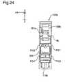
- FIG 24shows a third diagram of the construction of the ink cartridge pertaining to Variation 14.
- the ink cartridge 100b pertaining to Variation 14includes housing 101b, board 200 and sensor 104b.
- the board 200is mounted on the lower side (Z-axis plus direction side) of the front face (Y-axis plus direction side face) of the housing 101 as with ink cartridge 100 in the embodiment. Configuration of the board 200 is identical with the board 200 in the embodiment.
- the sensor 104bis embedded in the side wall of the housing 101 b and used for detection of remaining ink level.
- Hook 120bthat engages with catching part of the holder 4b when the ink cartridge 100b is attached to the holder 4b is mounted on the upper side of the front face of the housing 101b. Hook 120b fixates the Ink cartridge 100b to the holder 4b.
- the insertion direction when the ink cartridge 100b is attached to the holder 4bis a direction of arrow R in FIG. 22 (Z-axis plus direction) as with the ink cartridge 100 in the embodiment.
- the housing 101bhas displacement preventers PO1 -PO4 on the side portion (x-axis direction side) of housing 101b close to the board 200.
- the displacement preventers PO1 -PO4comes into contact with or close to a corresponding potion of the side wall of the holder 4b when the ink cartridge 100b is attached to the holder 4b. This prevents the ink cartridge 100b from moving in X-axial direction from its ideal position on the holder 4b.
- the displacement preventers PO1 and PO2are located on the upper side of the board 200 and prevent the upper side of the 100b from swinging in X-axial direction taking the ink supply orifice 110b as an axis of rotation.
- the displacement preventers PO3 and PO4are lateral to the terminals 210 -290 on the board 200 ( FIG. 3 ) and keep the terminals 210 -290 in the correct position so as to contact the corresponding apparatus-side terminal 410 -490 correctly.
- the electrical arrangements of the ink cartridge 100b pertaining to Variation 14is identical with those of the ink cartridge 100 pertaining to above-embodiment described with reference to FIG. 7 . So, the description thereof is omitted.
- the ink cartridge 100b pertaining to Variation 14affords the following working effects in addition to the same working effects as the ink cartridge 100 pertaining to the embodiment. Since the ink cartridge 100b has the displacement preventers PO1 -P04, it can prevent or reduce the position displacement when the ink cartridge 100b is attached to the holder 4b. Especially, since the displacement preventers PO3 and PO4 are lateral to the terminals 210 -290 on the board 200, accuracy of positioning of the terminals 210 -290 relative to the corresponding apparatus-side terminals can be improved. Further, as described with reference to FIG.
- the sensor drive terminal 250 and the second sensor drive terminal 290are arranged at each end of the terminals 210 -290, that is , the sensor drive terminal 250 and the second sensor drive terminal 290 are closest to the displacement preventers PO4 and PO4 respectively. This lead to improvement of accuracy of positioning of the sensor drive terminal 250 and the second sensor drive terminal 290. Therefore, the false contact between the terminals 250, 290 to which high voltage is applied and one of the non-corresponding apparatus-side terminals can be prevented or reduced.
- one of the boards 200b- 200s shown in FIGS. 14 -19can be mounted on the ink cartridge 100b shown in FIG. 22- 24 .
- porous elements POmay be disposed within the depressed portions DE in Variation 10 and Variation 11 described above, i.e. between the terminals 150, 190 and the board.
- ink drops or condensed waterwhich can easily cause shorting of the terminals 150, 190 to other terminals, can be effectively absorbed by the porous elements PO. Accordingly, this design also affords advantages analogous to those of Variation 10 and Variation 11 discussed above.
- the ink cartridge 100is furnished with a sensor 104 (piezoelectric element) and memory 203 as the plurality of the devices; however, the plurality of the devices are not limited to a sensor 104 and memory 203.
- the sensor 104may be a sensor of a type that detects the properties or level of ink by means of applying voltage to the ink within an ink cartridge 100, and measuring its resistance.
- the sensor 104is mounted on the housing 101 and the memory 203 is mounted on the board 200.
- the arrangements of the plurality of the devicesare not limited to those in the embodiment.
- the memory 203 and the board 200may be separate, and the memory 203 and the board 200 may be installed on the housing 101 individually.
- the plurality of the devicesmay be integrated into a circuit board or a single module.
- the circuit board or the single modulemay be mounted on the housing 101 or the board 200. It's preferred that terminals connected to a device to which relatively high voltage among the plurality of the devices are arranged in positions of the first sensor drive terminal 250 and the second sensor drive terminal 290 described above, and terminals connected to a device to which relatively low voltage among the plurality of the devices are arranged in positions of the terminals 220, 230, 260-280. In this case, damage to the ink cartridge 100 and the printing apparatus 1000 caused by shorting between the terminal connected to the device to which relatively high voltage and the terminal connected to the device to which relatively low voltage can be prevented or reduced.
- terminals for memory 203(220, 230, 260-280) and two terminals for sensor 104 (250, 290) are employed, however, other number of terminals may be employed due to the specification of the device.
- the terminal connected to the device to which relatively high voltagemay be one. In this case, such terminal may be arranged in a position of any of the terminals 250, 290 described above.
- the inventionis implemented in an ink cartridge 100, implementation thereof is not limited to ink cartridges, with implementation in a similar manner to receptacles containing other types of printing material, such as toner, being possible as well.
- portions of these arrangements implemented through hardwarecould instead be implemented through software, and conversely portions implemented through software could instead be implemented through hardware.
Landscapes
- Ink Jet (AREA)
- Accessory Devices And Overall Control Thereof (AREA)
- Coupling Device And Connection With Printed Circuit (AREA)
- Printing Elements For Providing Electric Connections Between Printed Circuits (AREA)
- Inking, Control Or Cleaning Of Printing Machines (AREA)
- Combinations Of Printed Boards (AREA)
- Electrophotography Configuration And Component (AREA)
- Measurement Of Levels Of Liquids Or Fluent Solid Materials (AREA)
- Pens And Brushes (AREA)
- Table Devices Or Equipment (AREA)
- Mirrors, Picture Frames, Photograph Stands, And Related Fastening Devices (AREA)
- Electric Connection Of Electric Components To Printed Circuits (AREA)
Description
- The present invention relates in general to a printing material container containing a printing material and a board mounted on the printing material container, and relates in particular to an arrangement for a plurality of terminals disposed on these components.
- In recent years, it has become common practice to equip ink cartridges used in ink jet printers or other printing apparatus, with a device, for example, a memory for storing information relating to the ink. Also disposed on such ink cartridges is another device, for example, a high voltage circuit (e.g. a remaining ink level sensor using a piezoelectric element) applied to higher voltage than the driving voltage of the memory. In such cases, there are instances in which the ink cartridge and the printing apparatus are electrically connected through terminals. There is proposed a structure for preventing the information storage medium from shorting and becoming damaged due to a drop of liquid being deposited on the terminals connecting the printing apparatus with the storage medium furnished to the ink cartridge.
- However, the technologies mentioned above do not contemplate an ink cartridge having equipped with a plurality of devices, for example, a memory and a high voltage circuit, with terminals for one device and the terminals for another device. With this kind of cartridge, there was a risk that shorting could occur between a terminal for the one device and the terminal for the another device. Such shorting caused the problem of possible damage to the ink cartridge or to the printing apparatus in which the ink cartridge is attached. This problem is not limited to ink cartridges, but is a problem common to receptacles containing other printing materials, for example, toner.
EP 1 219 437 discloses a circuit board for a printing container for mounting on a printing apparatus having the features of the preambles ofclaims 1 and 37 respectively.- An advantage of some aspects of the present invention is to provide a printing material container having a plurality of devices, wherein damage to the printing material container and the printing apparatus caused by shorting between terminals can be prevented or reduced.
- The present invention provides a printing material container according to claim 1, and a board, connectable to a printing apparatus according to claim 31.
- The above and other objects, characterizing features, aspects and advantages of the present invention will be clear from the description of preferred embodiments presented below along with the attached figures.
FIG. 1 shows a perspective view of the construction of the printing apparatus pertaining to an embodiment of the invention;FIG. 2 shows a perspective view of the construction of the ink cartridge pertaining to the embodiment;FIGS. 3A-B show diagrams of the construction of the board pertaining to the embodiment;FIG. 4 shows an illustration showing attachment of the ink cartridge in the holder;FIG. 5 shows an illustration showing the ink cartridge attached to the holder;FIGS. 6A-B show schematics of the construction of the contact mechanism;FIG. 7 shows a brief diagram of the electrical arrangement of the ink cartridge and the printing apparatus;FIG. 8 shows a brief diagram of the electrical arrangement, focusing on the cartridge detection/short detection circuit;FIG. 9 shows a flowchart depicting the processing routine of the cartridge determination process;FIGS. 10A-C show illustrations depicting three types of terminal lines on the board;FIG. 11 shows a flowchart depicting the processing routine of the remaining ink level detection process;FIGS. 12A-C show timing charts depicting temporal change in the shorting-detection enable signal and sensor voltage during execution of the remaining ink level detection process;FIG. 13 shows an illustration of a scenario of shorting;FIGS. 14A-D show first diagrams depicting boards pertaining to variations;FIGS. 15A-C show second diagrams depicting boards pertaining to variations;FIGS. 16A-D show third diagrams depicting boards pertaining to variations;FIGS. 17A-D show diagrams depicting the construction around boards of ink cartridges pertaining to variations;FIGS. 18A-D show cross sections A-A to D-D inFIG. 17 ;FIGS. 19A-D show fourth diagrams depicting boards pertaining to variations;FIG 20 shows a perspective view of the construction of the ink cartridge pertaining to a variation;FIG 21 shows a picture of the ink cartridge pertaining to a variation being attached to the printer;FIG 22 shows a first diagram of the construction of the ink cartridge pertaining to a variation;FIG 23 shows a second diagram of the construction of the ink cartridge pertaining to a variation;FIG 24 shows a third diagram of the construction of the ink cartridge pertaining to a variation.- Embodiments of the present invention will be described below with reference to the drawings.
- Arrangement of Printing apparatus and Ink Cartridge:
FIG. 1 shows a perspective view of the construction of the printing apparatus pertaining to an embodiment of the invention. Theprinting apparatus 1000 has a sub-scan feed mechanism, a main scan feed mechanism, and a head drive mechanism. The sub-scan feed mechanism carries the printing paper P in the sub-scanning direction using apaper feed roller 10 powered by a paper feed motor, not shown. The main scan feed mechanism uses the power of a carriage motor 2 to reciprocate in the main scanning direction acarriage 3 connected to a drive belt. The head drive mechanism drives aprint head 5 mounted on thecarriage 3, to eject ink and form dots. Theprinting apparatus 1000 additionally comprises amain control circuit 40 for controlling the various mechanisms mentioned above. Themain control circuit 40 is connected to thecarriage 3 via aflexible cable 37.- The
carriage 3 comprises aholder 4, theprint head 5 mentioned above, and a carriage circuit, described later. Theholder 4 is designed for attachment of a number of ink cartridges, described later, and is situated on the upper face of theprint head 5. In the example depicted inFIG. 1 , theholder 4 is designed for attachment of four ink cartridges, e.g. individual attachment of four types of ink cartridge containing black, yellow, magenta, and cyan ink. Four openable andclosable covers 11 are attached to theholder 4 for each attached ink cartridge. Also disposed on the upper face of theprint head 5 are ink supply needles 6 for supplying ink from the ink cartridges to theprint head 5. - The construction of the ink cartridge pertaining to the embodiment will now be described with reference of
FIGS. 2 -5 .FIG. 2 shows a perspective view of the construction of the ink cartridge pertaining to the embodiment.FIGS. 3A-B show diagrams of the construction of the board pertaining to the embodiment.FIG. 4 shows an illustration showing attachment of the ink cartridge in the holder.FIG. 5 shows an illustration showing the ink cartridge attached to the holder. Theink cartridge 100 attached to theholder 4 comprises ahousing 101 containing ink, alid 102 providing closure to the opening of thehousing 101, aboard 200, and asensor 104. On the bottom face of thehousing 101 there is formed anink supply orifice 110 into which the aforementionedink supply needle 6 inserts whenink cartridge 100 is attached to theholder 4. At the upper edge of the front face FR of thehousing 101 there is formed a flaredsection 103. On the lower side of the center of the front face FR of thehousing 101 there is formed arecess 105 bounded by upper andlower ribs aforementioned board 200 fits into thisrecess 105. Thesensor 104 is located in the region posterior to theboard 200. Thesensor 104 is used to detect remaining ink level, as will be described later. FIG. 3A depicts the arrangement on the surface of theboard 200. This surface is the face that is exposed to the outside when theboard 200 is mounted on theink cartridge 100.FIG. 3B depicts theboard 200 viewed from the side. Aboss slot 201 is formed at the upper edge of theboard 200, and a boss hole 202 is formed at the lower edge of theboard 200. As shown inFIG. 1 , with theboard 200 attached to therecess 105 of thehousing 101,bosses recess 105 mate with theboss slot 201 and the boss hole 202 respectively. The distal ends of thebosses board 200 is secured within therecess 105 thereby.- The following description of attachment of the
ink cartridge 100 makes reference toFIG. 4 andFIG. 5 . As depicted inFIG. 4 , thecover 11 is designed to be rotatable about arotating shaft 9. With thecover 11 rotated upward to the open position, when theink cartridge 100 is being attached to the holder, the flaredsection 103 of the ink cartridge is received by aprojection 14 of thecover 11. When thecover 11 is closed from this position, theprojection 14 rotates downward, and theink cartridge 100 descends downward (in the Z direction inFIG. 4 ). When thecover 11 is completely closed, ahook 18 of thecover 11 interlocks with ahook 16 of theholder 4. With thecover 11 completely closed, theink cartridge 100 is secured pressed against theholder 4 by anelastic member 20. Also, with thecover 11 completely closed, theink supply needle 6 inserts into theink supply orifice 110 of theink cartridge 100, and the ink contained in theink cartridge 100 is supplied to theprinting apparatus 1000 via theink supply needle 6. As will be apparent from the preceding description, theink cartridge 100 is attached to theholder 4 by means of inserting it so as to move in the forward direction of the Z axis inFIG. 4 andFIG. 5 . The forward direction of the Z axis inFIG. 4 andFIG. 5 shall also be referred to as insertion direction of theink cartridge 100. - Returning to
FIG. 3 , theboard 200 shall be described further. The arrow R inFIG. 3 (a) indicates the insertion direction of theink cartridge 100 discussed above. As depicted inFIG. 3 , theboard 200 comprises amemory 203 disposed on its back face, and a terminal group composed of nine terminals 210 -290 disposed on its front face. Thememory 203 stores information relating to the ink contained in theink cartridge 100. The terminals 210 -290 are generally rectangular in shape, and are arranged in two rows generally orthogonal to the insertion direction R. Of the two rows, the row on the insertion direction R side, i.e. the row situated on the lower side inFIG. 3 (a) , shall be termed the lower row, and the row on the opposite side from the insertion direction R, i.e. the row situated on the upper side inFIG. 3 (a) , shall be termed the upper row. The terminals arranged so as to form the upper row consist, in order from left inFIG. 3 (a) , of a firstshort detection terminal 210, aground terminal 220, apower supply terminal 230, and a secondshort detection terminal 240. The terminals arranged so as to form the lower row consist, in order from left inFIG. 3 (a) , of a firstsensor drive terminal 250, areset terminal 260, aclock terminal 270, adata terminal 280, and a secondsensor drive terminal 290. As depicted inFIG. 3 , each of the terminals 210 -290 contains in its center portion a contact portion CP for contacting a corresponding terminal among the plurality of apparatus-side terminals, described later. - The terminals 210 -240 forming the upper row and the terminals 250 - 290 forming the lower row are arranged differently from one another, constituting a so-called staggered arrangement, so that the terminal centers do not line up with one another in the insertion direction R. As a result, the contact portions CP of the terminals 210 -240 forming the upper row and the contact portions CP of the terminals 250 -290 forming the lower row are similarly arranged differently from one another, constituting a so-called staggered arrangement.
- As will be appreciated from
FIG. 3A , the firstsensor drive terminal 250 is situated adjacently to two other terminals (thereset terminal 260 and the first short detection terminal 210), and of these, the firstshort detection terminal 210 for detecting shorting is positioned closest to the first sensor drive-terminal 250. Similarly, the secondsensor drive terminal 290 is situated adjacently to two other terminals (the secondshort detection terminal 240 and the data terminal 280), and of these, the secondshort detection terminal 240 for detecting shorting is positioned closest to the secondsensor drive terminal 290. - With regard to relationships among the contact portions CP, the contact portion CP of the first
sensor drive terminal 250 is situated adjacently to the contact portions CP of two other terminals (thereset terminal 260 and the first short detection terminal 210). Similarly, the contact portion CP of the secondsensor drive terminal 290 is situated adjacently to the contact portions CP of two other terminals (the secondshort detection terminal 240 and the data terminal 280). - As will be appreciated from
FiG. 3A , the firstsensor drive terminal 250 and the secondsensor drive terminal 290 are situated at the ends of the lower row, i.e. at the outermost positions in the lower row. The lower row is composed of a greater number of terminals than the upper row, and the length of the lower row in the direction orthogonal to the insertion direction R is greater than the length of the upper row, and consequently of all the terminals 210 -290 contained in the upper and lower rows, the firstsensor drive terminal 250 and the secondsensor drive terminal 290 are situated at the outermost positions viewed in the direction orthogonal to the insertion direction R. - With regard to relationships among the contact portions CP, the contact portion CP of the first
sensor drive terminal 250 and the contact portion CP of the secondsensor drive terminal 290 are respectively situated at the ends of the lower row formed by the contact portions CP of the terminals, i.e., at the outermost positions in the lower row. Among the contact portions of all the terminals 210 -290 contained in the upper and lower rows, the contact portion CP of the firstsensor drive terminal 250 and the contact portion CP of the secondsensor drive terminal 290 are situated at the outermost positions viewed in the direction orthogonal to the insertion direction R. - As will be appreciated from
FIG. 3A , the firstshort detection terminal 210 and the secondshort detection terminal 240 are respectively situated at the ends of the upper row, i.e., at the outermost positions in the upper row. As a result, the contact portion CP of the firstshort detection terminal 210 and the contact portion CP of the secondshort detection terminal 240 are similarly located at the ends of the upper row formed by the contact portions CP of the terminals, i.e. at the outermost positions in the upper row. Consequently, as will be discussed later, theterminals memory 203 are situated between the firstshort detection terminal 210 and the firstsensor drive terminal 250, and the secondshort detection terminal 240 and the secondsensor drive terminal 290, located to either side. - In the embodiment, the
board 200 has width of approximately 12.8 mm in the insertion direction R, width of the approximately 10.1 mm in the direction orthogonal to the insertion direction R, and thickness of approximately 0.71 mm. The terminals 210 -290 each have width of approximately 1.8 mm in the insertion direction R and width of approximately 1.05 mm in the direction orthogonal to the insertion direction R. The dimension values given here are merely exemplary, with differences on the order of ± 0.5 mm being acceptable, for example. The spacing between adjacent terminals in a given row (the lower row or the upper row), for example the interval K between the firstshort detection terminal 210 and theground terminal 220, is 1 mm for example. With regard to spacing among terminals, differences on the order of ± 0.5 mm are acceptable, for example. The interval J between the upper row and the lower row is about 0.2 mm. With regard to spacing among rows, differences on the order of ± 0.3 mm are acceptable, for example. - As depicted in
FIG. 5 , with theink cartridge 100 attached completely within theholder 4, the terminals 210 -290 of theboard 200 are electrically connected to acarriage circuit 500 via acontact mechanism 400 disposed on theholder 4. Thecontact mechanism 400 shall be described briefly making reference toFIGS. 6A-B . FIGS. 6A-B show schematics of the construction of thecontact mechanism 400. Thecontact mechanism 400 hasmultiple slits board 200. Within each slit 401, 402 there fits acontact forming member contact forming member board 200. InFIG. 6A , portions 410 -490 which are the portions of thecontact forming members printing apparatus 1000 with the terminals 210 -290. The portions 410 -490 that contact the terminals 210 -290 shall hereinafter be termed apparatus-side terminals 410 -490. With theink cartridge 100 attached to theholder 4, the apparatus-side terminals 410 -490 respectively contact the contact portions CP of the terminals 210 -290 described above (FIG. 3A ).- On the other hand, of the two ends of each
contact forming member holder 4 is placed in resilient contact with a corresponding terminal among the terminals 510 -590 furnished to thecarriage circuit 500. - The electrical arrangements of the
ink cartridge 100 and the printing apparatus will now be described, focusing on the part relating to theink cartridge 100, with reference toFIG. 7 andFIG. 8 .FIG. 7 shows a brief diagram of the electrical arrangement of the ink cartridge and the printing apparatus.FIG. 8 shows a brief diagram of the electrical arrangement, focusing on the cartridge detection/short detection circuit. - First, the electrical arrangement of the
ink cartridge 100 shall be described. Of the terminals of theboard 200 described with reference toFIG. 3 , theground terminal 220, thepower supply terminal 230, thereset terminal 260, theclock terminal 270 and thedata terminal 280 are electrically connected to thememory 203. Thememory 203 is, for example, EEPROM comprising serially accessed memory cells, and performing data read/write operations in sync with a clock signal. Theground terminal 220 is grounded via a terminal 520 on theprinting apparatus 1000 side. Thereset terminal 260 is electrically connected to aterminal 560 of thecarriage circuit 500, and is used to supply a reset signal RST to thememory 203 from thecarriage circuit 500. Theclock terminal 270 is electrically connected to aterminal 570 of thecarriage circuit 500, and is used to supply the clock signal CLK to thememory 203 from thecarriage circuit 500. Thedata terminal 280 is electrically connected to aterminal 580 of thecarriage circuit 500, and is used for exchange of data signals SDA between thecarriage circuit 500 and thememory 203. - Of the terminals of the
board 200 described with reference toFIG. 3 , either the firstshort detection terminal 210, the secondshort detection terminal 240, or both are electrically connected with theground terminal 220. In the example depicted inFIG. 7 , it will be apparent that the firstshort detection terminal 220 is electrically connected to theground terminal 220. The firstshort detection terminal 210 and the secondshort detection terminal 240 are electrically connected respectively to theterminals carriage circuit 500, and used for cartridge detection and short detection, described later. - In the embodiment, a piezoelectric element is used as the
sensor 104. The remaining ink level can be detected by applying driving voltage to the piezoelectric element to induce the piezoelectric element to vibrate through the inverse piezoelectric effect, and measuring the vibration frequency of the voltage produced by the piezoelectric effect of the residual vibration. Specifically, this vibration frequency represents the characteristic frequency of the surrounding structures (.e.g. thehousing 101 and ink) that vibrate together with the piezoelectric element. The characteristic frequency changes depending on the amount of ink remaining within the ink cartridge, so the remaining ink level can be detected by measuring this vibration frequency. Of the terminals of theboard 200 described with reference toFIG. 3 , the secondsensor drive terminal 290 is electrically connected to one electrode of the piezoelectric element used as thesensor 104, and the firstsensor drive terminal 250 is electrically connected to the other electrode. Theseterminals sensor 104, between thecarriage circuit 500 and thesensor 104. - The
carriage circuit 500 comprises amemory control circuit 501, a cartridge detection/short detection circuit 502, and asensor driving circuit 503. Thememory control circuit 501 is a circuit connected to theterminals carriage circuit 500 mentioned above, and used to control thememory 203 of theink cartridge 100 to perform data read/write operations. Thememory control circuit 501 and thememory 203 are low-voltage circuits driven at relatively low voltage (in the embodiment, a maximum of about 3.3 V). Thememory control circuit 501 can employ a known design, and as such need not be described in detail here. - The
sensor driving circuit 503 is a circuit connected to theterminals carriage circuit 500, and used to control the driving voltage output from theseterminals sensor 104, causing thesensor 104 to detect the remaining ink level. As will be described later, the driving voltage has a generally trapezoidal shape, and contains relatively high voltage (in the embodiment, about 36 V). Specifically, thesensor driving circuit 503 and thesensor 104 are high-voltage circuits using relatively high voltage via theterminals sensor driving circuit 503 is composed of a logic circuit for example, but need not be described in detail herein. - The cartridge detection/
short detection circuit 502, like thememory control circuit 501, is a low-voltage circuit driven using relatively low voltage (in the embodiment, a maximum of about 3.3V). As depicted inFIG. 8 , the cartridge detection/short detection circuit 502 comprises afirst detection circuit 5021 and a second detection circuit 5022. Thefirst detection circuit 5021 is connected to theterminal 510 of thecarriage circuit 500. Thefirst detection circuit 5021 has a cartridge detection function for detecting whether there is contact between the terminal 510 and the firstshort detection terminal 210 of theboard 200, and a short detection function for detecting shorting of the terminal 510 to theterminals - To describe in more specific terms, the
first detection circuit 5021 has a reference voltage V_ref1 applied to one end of two series-connected resistors R2, R3, with the other end being grounded, thereby maintaining the potential at point P1 and P2 inFIG. 4 at V_ref1 and V_ref2, respectively. Herein V_ref1 shall be termed the short detection voltage, and V_ref2 shall be termed the cartridge detection voltage. In the embodiment, the short detection voltage V_ref1 is set to 6.5 V, and the cartridge detection voltage V_ref2 is set to 2.5 V. These values are established by means of the circuits, and are not limited to the values given herein. - As depicted in
FIG. 8 , the short detection voltage V_ref1 (6.5 V) is input to the negative input pin of a first Op-Amp OP1, while the cartridge detection voltage V_ref2 (2.5 V) is input to the negative input pin of a second Op-Amp OP2. The potential of the terminal 510 is input to the positive input pins of the first Op-Amp OP1 and the second Op-Amp OP2. These two Op-Amps function as a comparator, outputting a High signal when the potential input to the negative input pin is higher than the potential input to the positive input pin, and conversely outputting a Low signal when the potential input to the negative input pin is lower than the potential input to the positive input pin. - As depicted in
FIG. 8 , the terminal 510 is connected to a 3.3 V power supply VDD 3.3 via a transistor TR1. By means of this arrangement, ifterminal 510 is free e.g. there is no contact withterminal 510, the potential of the terminal 510 will be set at about 3 V. As noted, when theink cartridge 100 is attached, the terminal 510 comes into contact with the firstshort detection terminal 210 of theboard 200 described previously. Here, as depicted inFIG. 7 , with the firstshort detection terminal 210 and theground terminal 220 electrically connected (shorted) in theboard 200, when the terminal 510 comes into contact with the first short detection terminal 210 (herein referred to as being in contact), the terminal 510 is electrically continuous with the groundedterminal 520, and the potential of the terminal 510 drops to 0 V. - Consequently, with the terminal 510 free, a High signal from the second Op-Amp OP2 is output as the cartridge detection signal CS1. With the terminal 510 in contact, a Low signal from the second Op-Amp OP2 is output as the cartridge detection signal CS1.
- On the other hand, if the terminal 510 is shorted to the
adjacent terminal 550, there are instances in which the sensor driving voltage (45 V max) will be applied to the terminal 510. As shown inFIG. 8 , when voltage greater than the short detection voltage V_ref1 (6.5 V) is applied to the terminal 510 due to shorting, a High signal from the Op-Amp OP1 will be output to an AND circuit AA. - As shown in
FIG. 8 , a short detection enable signal EN is input from themain control circuit 40 to the other input pin of the AND circuit AA. As a result, only during the time interval that a High signal is input as the short detection enable signal EN, thefirst detection circuit 5021 outputs the High signal from the Op-Amp OP1 as a short detection signal AB1. That is, execution of the short detection function of thefirst detection circuit 5021 is controlled by means of the short detection enable signal EN of themain control circuit 40. The short detection signal AB1 from the AND circuit AA is output to themain control circuit 40, as well as being output to the base pin of the transistor TR1 via resistance R1. As a result, by means of the transistor TR1 it is possible to prevent high voltage from being applied to the power supply VDD 3.3 via the terminal 510 when a short is detected (when the short detection signal AB1 is HI). - The second detection circuit 5022 has a cartridge detection function for detecting whether there is contact between the terminal 540 and the second
short detection terminal 240 of theboard 200, and a short detection function for detecting shorting of the terminal 540 to theterminals first detection circuit 5021, a detailed illustration and description need not be provided here. Hereinafter, the cartridge detection signal output by the second detection circuit 5022 shall be denoted as CS2, and the short detection signal as AB2. - An arrangement of the
carriage circuit 500 corresponding to asingle ink cartridge 100 has been described above. In the embodiment, since fourink cartridges 100 are attached, four of the cartridge detection/short detection circuits 502 described above will be provided, at each of the attachment locations for the fourink cartridges 100. While only a singlesensor driving circuit 503 is provided, and a singlesensor driving circuit 503 is connectable to each of thesensors 104 of theink cartridges 100 attached at the four attachment locations by means of a switch(not shown). Thememory control circuit 501 is a single circuit responsible for processes relating to the four ink cartridges. - The
main control circuit 40 is a computer of known design comprising a central processing unit (CPU), a read-only memory (ROM), and a random access memory (RAM). As noted, themain control circuit 40 controls the entire printer; inFIG. 8 , however, only those elements necessary for description of the embodiment are selectively illustrated, and the following description refers to the illustrated arrangement. Themain control circuit 40 comprises a cartridge determining module M50 and a remaining ink level determining module M60. On the basis of the received cartridge detection signals CS1, CS2, the cartridge determining module M50 executes a cartridge determination process, described later. The remaining ink level determining module M60 controls thesensor driving circuit 503, and executes a remaining ink level detection process, described later. - The cartridge determination process executed by the cartridge determining module M50 of the
main control circuit 40 will be described with reference toFIG. 9 andFIG. 10 .FIG. 9 shows a flowchart depicting the processing routine of the cartridge determination process.FIGS. 10A-C show illustrations depicting three types of terminal lines on theboard 200. - Before turning to the cartridge determination process, the
board 200 will be described further with reference toFIG. 10 . Theboard 200 mentioned previously comes in three types, depending on the wiring pattern of the firstshort detection terminal 210, the secondshort detection terminal 240, and theground terminal 220. These three types are designated respectively as Type A, Type B, and Type C. As depicted inFIG. 10A , theType A board 200 is arranged with the firstshort detection terminal 210 and theground terminal 220 electrically connected by a conductingline 207, while the secondshort detection terminal 240 and theground terminal 220 are not electrically connected. As depicted inFIG. 10B , theType B board 200 is arranged with both the firstshort detection terminal 210 and the secondshort detection terminal 240 electrically connected with theground terminal 220 by a conductingline 207. As depicted inFIG. 10C , theType C board 200 is arranged with the secondshort detection terminal 240 and theground terminal 220 electrically connected by a conductingline 207, while the firstshort detection terminal 210 and theground terminal 220 are not electrically connected. Aboard 200 of predetermined type, selected with reference to ink type or ink quantity for example, is disposed on theink cartridge 100. Specifically, depending on the quantity of ink contained in theink cartridge 100, aType A board 200 could be disposed on an L size cartridge containing a large quantity of ink; aType B board 200 could be disposed on an M size cartridge containing a standard quantity of ink; and aType C board 200 could be disposed on an S size cartridge containing a small quantity of ink. - The cartridge determining module M50 of the
main control circuit 40 constantly receives from the cartridge detection/short detection circuit 502 the cartridge detection signals CS1, CS2 for each of the four attachment locations of theholder 4, and using these signals executes the cartridge determination process for each of the attachment locations. - When the cartridge determining module M50 initiates the cartridge determination process for a selected attachment location, the cartridge determining module M50 first ascertains whether the cartridge detection signal CS1 from the cartridge detection/
short detection circuit 502 in the selected attachment location is a Low signal (Step S102). Next, the cartridge determining module M50 ascertains whether the cartridge detection signal CS2 in the selected attachment location is a Low signal (Step S104 or S106). If as a result the cartridge detection signals CS1 and CS2 are both Low signals (Step S102: YES and Step S104: YES), the cartridge determining module M50 decides that theink cartridge 100 attached to the selected attachment location is furnished with the Type B board 200 (Step S108). - Similarly, the cartridge determining module M50, in the event that the cartridge detection signal CS1 is a Low signal and the cartridge detection signal CS2 is a High signal (Step S102: YES and Step S104: NO), decides that the ink cartridge is furnished with the Type A board 200 (Step S110); or in the event that the cartridge detection signal CS1 is a High signal and the cartridge detection signal CS2 is a Low signal (Step S102: NO and Step S104: YES), decides that the ink cartridge is furnished with the
Type C board 200 described above (Step S112). - In the event that both the cartridge detection signals CS1 and CS2 are High signals Step S102: NO and Step S104: NO), the cartridge determining module M50 decides that no cartridge is attached to the selected attachment location (Step S114). In this way, the cartridge determining module M50 determines whether an
ink cartridge 100 is attached, and if so what type, for each of the four attachment locations. - The remaining ink level detection process executed by the remaining ink level determining module M60 of the
main control circuit 40 will now be described with reference toFIG. 11 andFIGS. 12A-C .FIG. 11 shows a flowchart depicting the processing routine of the remaining ink level detection process.FIGS. 12A-C show timing charts depicting temporal change in the shorting-detection enable signal and sensor voltage during execution of the remaining ink level detection process; - The remaining ink level determining module M60 of the
main control circuit 40, in the event that the remaining ink level in theink cartridge 100 attached at any of the attachment locations of theholder 4 is to be detected, first sets to High the short detection enable signal EN to all of the cartridge detection/short detection circuits 502 (Step S202). As a result, the short detection function is enabled in all of the cartridge detection/short detection circuits 502, and if voltage above the reference voltage V_ref1 (6.5 V) is applied to theaforementioned terminal 520 and terminal 540, are able to output High signals as the short detection signals AB1, AB2. In other words, a state in which the short detection enable signal EN are High signals is a state in which shorting of the terminal 510 or terminal 540 to the terminal 550 or terminal 590 is monitored. - Next, the remaining ink level determining module M60 instructs the
sensor driving circuit 503 to output driving voltage from the terminal 550 or terminal 590 to thesensor 104, and detect the remaining ink level output (Step S204). To describe in more specific terms, when thesensor driving circuit 503 receives an instruction signal from the remaining ink level determining module M60, thesensor driving circuit 503 outputs driving voltage from either the terminal 550 or the terminal 590, the voltage being applied to the piezoelectric element which constitutes thesensor 104 of theink cartridge 100, charging the piezoelectric element and causing it to distort by means of the inverse piezoelectric effect. Thesensor driving circuit 503 subsequently drops the applied voltage, whereupon the charge built up in the piezoelectric element is discharged, causing the piezoelectric element to vibrate. InFIG. 12 , the driving voltage is the voltage shown during time interval T1. As depicted inFIG. 12 , the driving voltage fluctuates between the reference voltage and the maximum voltage Vs in such a way as to describe a trapezoidal shape. The maximum voltage Vs is set to relatively high voltage (e.g. about 36 V). Via theterminal 550 of the terminal 590, thesensor driving circuit 503 detects the voltage produced by the piezoelectric effect as a result of vibration of the piezoelectric element (inFIG. 12 depicted as the voltage during time interval T2), and by measuring the vibration frequency thereof detects the remaining ink level. Specifically, this vibration frequency represents the characteristic frequency of the surrounding structures (thehousing 101 and ink) that vibrate together with the piezoelectric element, and changes depending on the amount of ink remaining within theink cartridge 100, so the remaining ink level can be detected by measuring this vibration frequency. Thesensor driving circuit 503 outputs the detected result to the remaining ink level determining module M60 of themain control circuit 40. - When the remaining ink level determining module M60 receives the detected result from the
sensor driving circuit 503, the remaining ink level determining module M60 brings the short detection enable signal EN, which was previously set to a High signal in Step S202, back to a Low signal (Step S206), and terminates the process. In this process, the interval that the remaining ink level is being detected is a state in which the short detection enable signal EN is set to a High signal to enable short detection. In other words, remaining ink level is detected while the occurrence of shorting is being monitored by the cartridge detection/short detection circuit 502. - The process carried out in the event that, during execution of detection of the remaining ink level (Step S204), the remaining ink level determining module M60 receives a High signal as the short detection signal AB1 or AB2, e.g. shorting is detected shall be described here. In
FIG. 11 , a flowchart of the interrupt processing routine when shorting is detected is shown as well. When the terminal 510 or the terminal 540 shorts to the terminal that is outputting the sensor driving voltage of theterminals terminal 510 orterminal 540. Thereupon, since the short detection enable signal EN is currently set to High, at the instant that the sensor driving voltage goes above the short detection voltage V_ref1 (6.5 V), a High signal will be output as the short detection signals AB1, AB2 from the cartridge detection/short detection circuit 502. When the remaining ink level determining module M60 receives either of these short detection signals AB1, AB2, the remaining ink level determining module M60 suspends detection of remaining ink level, and executes the interrupt processing when shorting is detected. - When the interrupt processing is initiated, the remaining ink level determining module M60 immediately instructs the
sensor driving circuit 503 to suspend the output of sensor driving voltage (Step S208). - Next, the remaining ink level determining module M60, without carrying out remaining ink level detection process to its conclusion, brings the short detection enable signal EN back to a Low signal (Step S206) to terminate the process. For example, the
main control circuit 40 may take some countermeasure, such as notifying the user of the shorting. FIG. 12A depicts change of the detection enable signal EN through time.FIG. 12B depicts sensor voltage in the event that neither the terminal 510 nor the terminal 540 is shorting to the terminal that outputs the sensor driving voltage of theterminals FIG. 12C depicts sensor voltage in the event that the terminal 510 or the terminal 540 is shorting to the terminal that, of theterminals - As depicted in
FIG. 12A , during execution of the remaining ink level detection process, the detection enable signal EN is a High signal. As shown inFIG. 12B , in the normal state (no shorting), after high voltage Vs has been applied to thesensor 104, the applied voltage drops, and subsequently vibration voltage is produced through the piezoelectric effect. In the embodiment, Vs is set at 36 V. - As depicted in
FIG. 12C , on the other hand, in the abnormal state (shorting), the sensor voltage drops at the instant that it goes above the short detection voltage V_ref1 (6.5 V). This is due to the fact that, at the instant that the sensor voltage goes above the short detection voltage V_ref1 (6.5 V), a High signal is output as the short detection signal AB1 or AB2 from the cartridge detection/short detection circuit 502 to the remaining ink level determining module M60, and the remaining ink level determining module M60 receiving this signal immediately drops the sensor driving voltage. FIG. 13 shows an illustration of a scenario of shorting. Here, the likely scenario for shorting to other terminals by theterminals FIG. 13 , in which an electrically conductive ink drop S1 or a water drop S2 formed by condensation has become deposited on theboard 200 of theink cartridge 100, bridging the gap between the firstsensor drive terminal 250 or the secondsensor drive terminal 290 and another terminal or terminals on theboard 200, producing shorting. For example, ink drop S1 that has adhered to the surface of thecarriage 3 orink supply needle 6 disperses and adheres as shown inFIG. 13 by the motion of attaching or detaching ofink cartridge 100. In this instance, when theink cartridge 100 is attached, the terminal 550 that outputs the sensor driving voltage, for example, will short to another terminal 510, 520, or 560 of thecarriage circuit 500 via the firstsensor drive terminal 250 and the terminals (FIG. 13 :terminals sensor drive terminal 250. Or, the terminal 590 that outputs the sensor driving voltage will short to anotherterminal 540 of thecarriage circuit 500 via the secondsensor drive terminal 290 and the second short detection terminal 240 (FIG. 13 ) bridged by the water drop S2 to the secondsensor drive terminal 290, for example. Such a shorting is caused by various factor as well as the adhesion of the ink drop. For example, the shorting may be caused by trapping electrically conducting object, for example, paper clip oncarriage 3. The shorting also may be caused by adhesion to terminals of the electrically conducting material, for example, skin oil of user.- As mentioned previously with reference to
FIG. 3 , in theink cartridge 100 pertaining to the embodiment the firstsensor drive terminal 250 and the secondsensor drive terminal 290 which apply the driving voltage to the sensor are arranged at the two ends of the terminal group, so the number of adjacent terminals is small. As a result, the likelihood of the firstsensor drive terminal 250 and the secondsensor drive terminal 290 shorting to other terminals is low. - On the
board 200, if the firstsensor drive terminal 250 should short to the adjacent firstshort detection terminal 210, the shorting will be detected by the aforementioned cartridge detection/short detection circuit 502. For example, shorting of the firstsensor drive terminal 250 to another terminal caused by the ink drop S1 infiltrating from the firstsensor drive terminal 250 side will be detected instantly and the output of sensor driving voltage will be suspend, preventing or reducing damage to thememory 203 and theprinting apparatus 1000 circuits (thememory control circuit 501 and the cartridge detection/short detection circuit 502) caused by the shorting. - Also, the first
short detection terminal 210 is adjacent to the firstsensor drive terminal 250 and situated closest to the firstsensor drive terminal 250. Consequently, in the event that the firstsensor drive terminal 250 should short to another terminal or terminals due to the ink drop S1 or the water drop S2, there is a high likelihood that the firstsensor drive terminal 250 will short to the firstshort detection terminal 210 as well. Consequently, shorting of the firstsensor drive terminal 250 to another terminal can be detected more reliably. - In addition to detecting shorting, the first
short detection terminal 210 is also used by the cartridge detection/short detection circuit 502 to determine whether anink cartridge 100 is attached, as well as to determine the type of attachedink cartridge 100. As a result, the number of terminals on theboard 200 can be kept down, and it becomes possible to reduce the number ofboard 200 manufacturing steps and the number of parts for theboard 200. - Similarly, if the second
sensor drive terminal 290 should short to the secondshort detection terminal 240, the short will be detected by the cartridge detection/short detection circuit 502. Consequently, shorting of the secondsensor drive terminal 290 to another terminal caused by the ink drop S1 or the water drop S2 infiltrating from the secondsensor drive terminal 290 side can be detected instantly. As a result, damage to the circuits of thememory 203 and theprinting apparatus 1000 caused by shorting can be prevented or reduced. Similarly, the secondshort detection terminal 240 is the terminal situated closest to the secondsensor drive terminal 290. Consequently, in the event that the secondsensor drive terminal 290 should short to another terminal or terminals due to the ink drop S1 or the water drop S2, there is a high likelihood that the secondsensor drive terminal 290 will short to the secondshort detection terminal 240 as well. Consequently, shorting of the secondsensor drive terminal 290 to another terminal can be detected more reliably. - The first
sensor drive terminal 250 and the firstshort detection terminal 210 on the one hand, and the secondsensor drive terminal 290 and the secondshort detection terminal 240 on the other, are situated at the ends of the terminal group so that the other terminals (220, 230, 260 -270) lie between them. Consequently, if foreign matter (the ink drop S1, water drop S2 etc.) should infiltrate from either side as indicated by the arrows inFIG. 13 , this infiltration can be detected before it infiltrates as far as the other terminals (220, 230, 260 - 270). Consequently, damage to the circuits of thememory 203 and theprinting apparatus 1000 due to infiltration of foreign matter can be prevented or reduced. - The first
sensor drive terminal 250 and the secondsensor drive terminal 290 are arranged in the row on the insertion direction R side (lower row). As a result, since theterminals terminals memory 203 and theprinting apparatus 1000 caused by infiltration of foreign matter can be prevented or reduced. - The terminal group of the
board 200 is arranged in a staggered pattern. As a result, unwanted contact of the terminals of theink cartridge 100 with the terminals of the printing apparatus 1000 (thecontact forming members - Variations of the
board 200 mounted to theink cartridge 100 shall be described with reference toFIGS. 14A -16B .FIGS. 14A-D show first diagrams depicting boards pertaining to variations.FIGS. 15A-C show second diagrams depicting boards pertaining to variations.FIGS. 16A-B show third diagrams depicting boards pertaining to variations. - On the
board 200b depicted inFIG. 14A , the firstshort detection terminal 210 is similar to the firstshort detection terminal 210 of theboard 200 of the embodiment, but has at its lower end an extended portion that reaches into proximity with the lower edge of the lower row. The extended portion is positioned between the firstsensor drive terminal 250 and thereset terminal 260 of the lower row. As a result, for example, even in the event of adhesion of an ink drop S3 as depicted inFIG. 14 (a) , shorting of the extended portion of theshort detection terminal 210 to the firstsensor drive terminal 250 will be detected. Like this, when the firstsensor drive terminal 250 and terminal other than the firstshort detection terminal 210 are shorting, there is a high possibility that the firstsensor drive terminal 250 and the firstshort detection terminal 210 are shorting and the sensor driving voltage is suspended. Accordingly, problems caused by shorting of the firstsensor drive terminal 250 to another terminal (in the example ofFIG. 14A , the reset terminal 260) can be prevented or reduced. - As shown in
FIG. 14A , the secondshort detection terminal 240 of theboard 200b is also similar in shape to the firstshort detection terminal 210 mentioned above, and shorting of the secondsensor drive terminal 290 to another terminal will also be detected more reliably. - The
board 200c depicted inFIG. 14B has, in addition to the arrangement of theboard 200b described above, also has an extended portion located at the upper side of the firstsensor drive terminal 250, and reaching into proximity with the upper edge of the upper row. As a result, even in the event of adhesion of an ink drop S4 as depicted inFIG. 14 (b) , shorting of theshort detection terminal 210 to the extended portion of the firstsensor drive terminal 250 will be detected. Like this, when the firstsensor drive terminal 250 and terminal other than the firstshort detection terminal 210 are shorting, there is a high possibility that the firstsensor drive terminal 250 and the firstshort detection terminal 210 are shorting and the sensor driving voltage is suspended. Accordingly, problems caused by shorting of the firstsensor drive terminal 250 to another terminal can be prevented or reduced. - As shown in
FIG. 14B , the secondsensor drive terminal 290 of theboard 200c is also similar in shape to the firstsensor drive terminal 250 mentioned above, and infiltration of an ink drop from the end, at the end at which the secondsensor drive terminal 290 is situated, can be detected instantly. - The
board 200d depicted inFIG. 14C differs from theboard 200 of the embodiment in that there is no secondshort detection terminal 240. In the case of theType A board 200 depicted inFIG. 10A , the secondshort detection terminal 240 does not carry out detection of contact by means of the cartridge detection/short detection circuit 502 (since there is no shorting to the ground terminal 220). Consequently, in the case of theType A board 200, the secondshort detection terminal 240 is used for short detection only and accordingly can be dispensed with. In this case as well, since the firstshort detection terminal 210 is at the location closest to the firstsensor drive terminal 250, when the firstsensor drive terminal 250 and terminal other than the firstshort detection terminal 210 are shorting, there is a high possibility that the firstsensor drive terminal 250 and the firstshort detection terminal 210 are shorting and the sensor driving voltage is suspended. Infiltration of an ink drop to secondsensor drive terminal 290 side will also be detected to a certain extent. InFIG. 14C , the symbol CP represents the location of contact with thecontact forming member 403 that would contact the secondshort detection terminal 240 if the secondshort detection terminal 240 were present (i.e. thecontact forming member 403 corresponding to theterminal 540 of the carriage circuit 500). Even in the case that the secondshort detection terminal 240 is absent, if a shorting should occur between the secondsensor drive terminal 290 and thecontact forming member 403 corresponding to theterminal 540 of thecarriage circuit 500 due to an ink drop S5, infiltration of the ink drop S5 will be detected. Similarly, in the case of aType C board 200, the firstshort detection terminal 210 may be dispensed with. - On the
board 200e depicted inFIG. 14D , the firstsensor drive terminal 250 and the firstshort detection terminal 210 have elongated shape reaching from the vicinity of the upper edge of the upper row to the vicinity of the lower edge of the lower row. The terminals of this shape, as the contact locations are indicated by the symbol CP inFIG. 14D , can contact the correspondingcontact forming portions 403 arranged in a staggered pattern. In the case of theboard 200e, like theboard 200c described previously, even if an ink drop S6 should become deposited for example, shorting between the extended portions of the firstshort detection terminal 210 and the firstsensor drive terminal 250 will be detected. Like this, firstshort detection terminal 210 is located between firstsensor drive terminal 250 and terminal other than the firstshort detection terminal 210. Accordingly, when the firstsensor drive terminal 250 and terminal other than the firstshort detection terminal 210 are shorting, there is a high possibility that the firstsensor drive terminal 250 and the firstshort detection terminal 210 are shorting and the sensor driving voltage is suspended. - The second
sensor drive terminal 290 and the secondshort detection terminal 240 of theboard 200e have shape similar to the firstsensor drive terminal 250 and the firstshort detection terminal 210 described above. Accordingly, when the secondsensor drive terminal 290 and terminal other than the secondshort detection terminal 240 are shorting, there is a high possibility that the secondsensor drive terminal 290 and the secondshort detection terminal 240 are shorting. As a result, the possibility preventing or reducing the problems caused by shorting of thesensor drive terminal - On the
board 200f depicted inFIG. 15A , the terminal which corresponds to the firstshort detection terminal 210 and theground terminal 220 in theboard 200 pertaining to the embodiment is anintegral terminal 215 wherein these two terminals are integrally formed as a single member. Thisboard 200f can be used in place of the Type A or Type B board 200 (FIG. 10 ) whose firstshort detection terminal 210 andground terminal 220 are shorted. With theboard 200f, the need is obviated for a line between the firstshort detection terminal 210 and theground terminal 220, which was required in the case of in theboard 200 pertaining to the embodiment, so theboard 200 requires fewer process steps and fewer parts. - On the
board 200g depicted inFIG. 15B , the terminals 210 -240 of the upper row each have shape similar to the firstshort detection terminal 210 of theboard 200b described previously. Specifically, each of the terminals 210 -240 has an extended portion situated at the lower edge of the corresponding terminal of theboard 200 pertaining to the embodiment and reaching into proximity with the lower edge of the lower row. The terminals 250 -290 of the lower row of theboard 200g are similar in shape to the firstsensor drive terminal 250 of theboard 200c described earlier. Specifically, the each of the terminals 250 -290 has an extended portion situated at the upper edge of the corresponding terminal of theboard 200 pertaining to the embodiment and reaching into proximity with the upper edge of the upper row. - As a result, the terminals 210 -290 of the
board 200g are arranged so as to form a terminal group composed of a single row of terminals of generally oar shape of in mutually different arrangement, rather than being arranged in two rows. The firstsensor drive terminal 250 and the secondsensor drive terminal 290 to which the high-voltage sensor driving voltage is applied are positioned at the two ends of the single row of the terminal group, with the firstshort detection terminal 210 and the secondshort detection terminal 240 respectively arranged adjacently inward from the firstsensor drive terminal 250 and the secondsensor drive terminal 290. - With the
board 200g, an ink drop or foreign matter infiltrating from either end can be detected immediately at the point in time that shorting occurs between the firstsensor drive terminal 250 and theshort detection terminal 210, or between the secondsensor drive terminal 290 and the secondshort detection terminal 240. In the event that the firstsensor drive terminal 250 or the secondsensor drive terminal 290 should short to another terminal, in the case where the shorting is due to an ink drop or the like, the likelihood is extremely high that shorting between the firstsensor drive terminal 250 and theshort detection terminal 210, or between the secondsensor drive terminal 290 and the secondshort detection terminal 240, will occur at the same time. Consequently, shorting of the firstsensor drive terminal 250 or the secondsensor drive terminal 290 to another terminal can be detected reliably. As a result, damage to thememory 203 and theprinting apparatus 1000 circuits (thememory control circuit 501 and the cartridge detection/short detection circuit 502) caused by the shorting can be prevented or minimized. - On the
board 200h depicted inFIG. 15C , the terminals 210 -290 have elongated shape extending over a distance equivalent to two rows of theboard 200 pertaining to the embodiment, in a manner similar to the firstsensor drive terminal 250 and the firstshort detection terminal 210 of theboard 200e described previously. The terminals of this shape, as the contact locations are indicated by the symbol cp inFIG. 15C , can contact the correspondingcontact forming portions 403 arranged in a staggered pattern. - In the
board 200h, the terminals 210 -290 are arranged so as to form a single row in the orthogonal direction to the insertion direction R, in a manner similar to theboard 200g described above. Also, like theboard 200g, the firstsensor drive terminal 250 and the secondsensor drive terminal 290 to which the high-voltage sensor driving voltage is applied are positioned at the two ends of the single row of terminals, with the firstshort detection terminal 210 and the secondshort detection terminal 240 respectively arranged adjacently inward from the firstsensor drive terminal 250 and the secondsensor drive terminal 290. As a result, theboard 200h affords advantages analogous to those of theboard 200g described above. - The first
short detection terminal 210 of theboard 200i depicted inFIG. 16A has a shape that is longer on the left side in the drawing, as compared to the firstshort detection terminal 210 of theboard 200 pertaining to the embodiment. Additionally, the firstshort detection terminal 210 of theboard 200i has an extended portion reaching from the left edge portion to the vicinity of the lower edge of the lower row. The extended portion is situated to the left of the firstsensor drive terminal 250 in the lower row. In other words, the extended portion is disposed to further from the middle of the terminal group in a direction substantially orthogonal to the insertion direction R than the firstsensor drive terminal 250. In this case, whereas viewed in terms of the terminal as a whole, the firstshort detection terminal 210 is situated outwardly (to the left side) of the firstsensor drive terminal 250, when viewed in terms of the contact portion CP of the terminal, of the contact portions CP of all of the terminals 210 -290 the contact portion CP of the firstsensor drive terminal 250 is the one situated at the outermost position (left side), in the same manner as in the embodiment. Also, shorting between the firstsensor drive terminal 250 and the firstshort detection terminal 210 that includes the contact portion CP adjacent to the contact portion CP of the firstsensor drive terminal 250 is detected. Accordingly, theboard 200i pertaining to this variation affords advantages similar to theboard 200 pertaining to the embodiment. Specifically, infiltration of an ink drop from the edge can be detected instantly, and damage to the circuits of thememory 203 and theprinting apparatus 1000 can be prevented or minimized. Additionally, since the firstshort detection terminal 210 has the extended portion, the length of a first portion that is a portion adjacent to the circumferential edge of the firstshort detection terminal 210 among the circumferential edge of the firstsensor drive terminal 250 becomes long. As shown inFIG. 16B , the length of the first portion is longer than that of a second portion that is a portion adjacent to the circumferential edge of thereset terminal 260 among the among the circumferential edge of the firstsensor drive terminal 250. As a result, when the firstsensor drive terminal 250 and terminal other than the firstshort detection terminal 210, for example, thereset terminal 260 are shorting, there is a high possibility that the firstsensor drive terminal 250 and the firstshort detection terminal 210 are shorting. Accordingly, the sensor driving voltage is suspended and problems caused by shorting of the firstsensor drive terminal 250 to another terminal can be prevented or reduced with higher probability. - The first
short detection terminal 210 of theboard 200p inFIG. 16C has the longer extended portion than the firstshort detection terminal 210 of theboard 200i. As shown inFIG 16C , the extended portion of the firstshort detection terminal 210 of theboard 200p extends from upper left to lower right of the firstsensor drive terminal 250 along the circumferential edge of the firstsensor drive terminal 250. As a result, the length of the first portion in theboard 200p is longer than that in theboard 200i. Accordingly, when the firstsensor drive terminal 250 and terminal other than the firstshort detection terminal 210 are shorting, there is a higher possibility the sensor driving voltage is suspended and problems caused by shorting of the firstsensor drive terminal 250 to another terminal can be prevented or reduced. - The first
short detection terminal 210 of the board 200q inFIG. 16D has the longer extended portion than the firstshort detection terminal 210 of theboard FIG 16D , the extended portion of the firstshort detection terminal 210 of the board 200q extends from upper left through lower to upper right of the firstsensor drive terminal 250 along the circumferential edge of the firstsensor drive terminal 250. In other words, the firstshort detection terminal 210 is formed so as to surround the firstsensor drive terminal 250 completely. As a result, the length of the first portion in the board 200q is longer than that in theboard sensor drive terminal 250 and terminal other than the firstshort detection terminal 210 are shorting, there is a higher possibility the sensor driving voltage is suspended and problems caused by shorting of the firstsensor drive terminal 250 to another terminal can be prevented or reduced. - As shown in
FIGS. 16A-C ,board short detection terminal 210 is located adjacently to a portion of thesensor drive terminal 250 by providing the extended portion of the firstshort detection terminal 210. Aboutboard 200i, the extended potion of the firstshort detection terminal 210 located adjacently to left border of the firstsensor drive terminal 250 in a lateral direction towards an edge of theink cartridge 100, and the firstshort detection terminal 210 itself is located adjacently to upper border of the firstsensor drive terminal 250 in opposite direction of the insertion direction R. Meanwhile, aboutboard 200p, in addition to above-mentioned two directions, the extended potion of the firstshort detection terminal 210 is located adjacently to lower border of the firstsensor drive terminal 250 in the insertion direction R. Furthermore, about board 200q, the extended potion of the firstshort detection terminal 210 is located adjacently to right border of the firstsensor drive terminal 250 in lateral direction away from an edge of theink cartridge 100. In other words, about board 200q, at least a potion of the firstshort detection terminal 210 is located adjacently to the firstsensor drive terminal 250 in all direction. - When the first
sensor drive terminal 250 and terminal other than the firstshort detection terminal 210 are shorting by ink drop or other object infiltrating from the direction in which the portion of the firstshort detection terminal 210 is located adjacently to the portion of the firstsensor drive terminal 250, there is a much high possibility that the firstsensor drive terminal 250 and the firstshort detection terminal 210 are shorting. Accordingly, problems caused by shorting of the firstsensor drive terminal 250 to another terminal by ink drop or other object infiltrating from such direction can be prevented or reduced with much high probability. In the present variations, the extended portion of the firstshort detection terminal 210 adds the direction in which the firstshort detection terminal 210 and the firstsensor drive terminal 250 are adjacent each other, and prevents or reduces problems caused by shorting of the firstsensor drive terminal 250 to another terminal with much high probability. - In the
boards short detection terminal 210 on the left side is furnished with a structure having the extended portion described above, but it would be possible to furnish the secondshort detection terminal 240 on the right side with a structure having an extended portion, in addition to the firstshort detection terminal 210 or instead of the firstshort detection terminal 210. In this case as well, there are afforded advantages analogous to those of theboards - The
board 200j depicted inFIG. 16B , like theboard 200f described previously inVariation 5, has anintegral terminal 215 wherein the firstshort detection terminal 210 and theground terminal 220 in theboard 200 pertaining to the embodiment are integrally formed as a single member. Theintegral terminal 215 of theboard 200j differs in shape from theintegral terminal 215 of theboard 200f described previously. Specifically, theintegral terminal 215 of theboard 200j, like the firstshort detection terminal 210 of theboard 200i described inVariation 8, has a shape elongated on the left side, and has an extended portion reaching from the left edge portion to the vicinity of the lower edge of the lower row. In this case, advantages analogous to those of theboard 200i pertaining toVariation 8 are attained, while reducing the number of production steps and parts needed for the board. - In the embodiment and variations described hereinabove, all of the terminals are situated on the
board 200, but it is not necessary that all terminals be situated on theboard 200. For example, it would be acceptable for some of the terminals to be situated on thehousing 101 of theink cartridge 100. By way of specific examples,Variation 10 andVariation 11 shall be described below with reference toFIGS. 17A -18D .FIGS. 17A-D show diagrams depicting the construction around boards of ink cartridges pertaining to variations.FIGS. 18A-D show cross sections A-A to D-D inFIG. 17 . - The
board 200k depicted inFIG. 17A is furnished with seven terminals 210 - 240 and 260 -280, out of the nine terminals 210 -290 furnished to theboard 200 of the embodiment. Out of the nine terminals 210 -290 furnished to theboard 200 of the embodiment, theboard 200k lacks the firstsensor drive terminal 250 and the secondsensor drive terminal 290. Theboard 200k pertaining to this variation is furnished with notches NT1 or NT2 situated in zones that include the locations where the firstsensor drive terminal 250 and the secondsensor drive terminal 290 were disposed on theboard 200 pertaining to the embodiment. The notches may have the shape indicated by the solid lines NT1, or the shape indicated by the broken lines NT2, inFIG. 17A .Terminals sensor drive terminal 250 and the secondsensor drive terminal 290 of theboard 200 in the embodiment are arranged on thehousing 101 situated to the rear of theboard 200k. Naturally, with theink cartridge 100 attached to theholder 4, theseterminals - A-A cross section viewed in
FIG. 17A is depicted inFIG. 18A . As shown inFIG. 18A , a depressed portion DE, formed by a gap between the notch NT1 of theboard 200k and the terminal 150, is situated between the terminal 150 and theadjacent terminals 260, 210 (inFIG. 18A , thereset terminal 260 is shown). While omitted from the drawing, a similar depressed portion DE is situated between the terminal 190 and theadjacent terminals - According to this variation, the following advantages are afforded in addition to those analogous to the
board 200 pertaining to the embodiment. If an ink drop or foreign matter should infiltrate from the end of theink cartridge 100 pertaining to this variation, it will become trapped in the depressed portion DE arranged surrounding the terminal 150 or the terminal 190, whereby shorting of the terminal 150 or the terminal 190 to another terminal due to an infiltrating ink drop or foreign matter can be further prevented or minimized. - The
board 200m depicted inFIG. 17B , rather than having the notches NT1 or NT2 pertaining toVariation 10, is instead furnished with through-holes HL situated at locations corresponding to the locations where the firstsensor drive terminal 250 and the secondsensor drive terminal 290 are situated on theboard 200 pertaining to the embodiment. B-B cross section viewed inFIG. 17B is depicted inFIG. 18B . Other arrangements of theink cartridge 100 pertaining toVariation 11 are the same as those of theink cartridge 100 pertaining toVariation 10. In this variation as well, depressed portions DE are situated between theterminals ink cartridge 100 pertaining to this variation affords advantages analogous to those of theink cartridge 100 pertaining toVariation 10. - In the boards pertaining to the embodiment and variations, all terminals are connected to one of
memory 203 andsensor 104. However, the board may include dummy terminal that is not connected to any device. An example of such type of the board will be described as Variation 12 with reference toFIGS. 19A-D. FIGS. 19A-D show fourth diagrams depicting boards pertaining to variations. - The
board 200r includes the upper row formed by four terminals and the lower row formed by five terminals, as with theboard 200 pertaining to the embodiment. Arrangement and function of the terminals 210 - 290 forming the upper row and the lower row ofboard 200r is the same as those of the terminals ofboard 200 in the embodiment, so the detailed description thereof is omitted. - The
board 200r shown inFIG. 19A has the dummy terminals DT between the upper row and the lower row and on the underside (the insertion direction side) of the lower row. The dummy terminals DT, for example, are made of the same material as other terminal 210-290.FIG. 19C shows E-E cross-section including dummy terminals DT. The dummy terminals DT has about the same thickness as other terminal 210-290. - The dummy terminals DT are for scraping away foreign object adherent on the
contact forming members 403, for example, dust whenink cartridge 100 is attached or detached. This enables to prevent foreign object from being brought to the terminal to be contacted by contact forming member 403 (for example, the firstsensor drive terminal 250 inFIG. 19C ) whenink cartridge 100 is attached or detached, and to prevent contact failure between the terminal and thecontact forming member 403. - The
board 200r shown inFIG. 19A has the dummy terminal DT between the firstsensor drive terminal 250 and theshort detection terminal 210, so you can't say firstsensor drive terminal 250 is located adjacent to firstshort detection terminal 210. However, the dummy terminals DT is not connected tomemory 203 and not connected to the apparatus-side terminals 510-590 onprinting apparatus 1000. Therefore, the shorting between the firstsensor drive terminal 250 and the dummy terminals DT never cause any problem. Accordingly, theboard 200r can afford working effects analogous to theboard 200 pertaining to the embodiment. That is to say, about theboard 200r, even if firstsensor drive terminal 250 is not located adjacent to firstshort detection terminal 210 in a precise sense, at least a portion of the firstshort detection terminal 210 is arranged relative to at least a portion of the firstsensor drive terminal 250, without a terminal connected to memory 203 (terminal 220, 230, 260-280) therebetween in at least one direction, for the detection of shorting between the firstsensor drive terminal 250 and the firstshort detection terminal 210. In such a case, the firstsensor drive terminal 250 is substantially located adjacent to firstshort detection terminal 210. Consequently, in the event that the firstsensor drive terminal 250 should short to another terminal or terminals due to the ink drop or the water drop, there is a high likelihood that the firstsensor drive terminal 250 will short to theshort detection terminal 210 as well. As a result, the output of sensor driving voltage is suspend and damage to the circuits of thememory 203 and theprinting apparatus 1000 caused by shorting can be prevented or reduced. - The boards pertaining to the embodiment and variations, as shown in
FIG. 2 , are described as the board mounted on aink cartridge 100 used for "on carriage" type printer. However, the boards pertaining to the embodiment and variations may be mounted on an ink cartridge used for "off carriage" type printer. The ink cartridge used for "off carriage" type printer will be described below with reference toFIG. 20 andFIG.21 .FIG 20 shows a perspective view of the construction of the ink cartridge pertaining to the variation 13.FIG 21 shows a picture of the ink cartridge pertaining to the variation 13 being attached to the printer. Ink cartridge 100b pertaining to Variation 13 is configured for installation in an "off carriage" type printer, i.e., one in which the ink cartridge is not installed on a carriage. Off carriage type printers are typically large-scale printers; the ink cartridges employed in such large-scale printers are typically larger in size than the ink cartridges employed in on-carriage type printers.Ink cartridge 100b comprises ahousing 1001 containing ink, aboard mounting portion 1050 for mountingboard 200, anink feed orifice 1020 for supplying ink from ahousing 1001 to the printer; anair feed orifice 1030 allowing intake of air intoink cartridge 100b to allow smooth flow of ink; and guideportions 1040 for installation in the printer. The exterior dimensions ofink cartridge 100b are such that the side thereof (i.e. the depth direction) extending perpendicular to the side on which theguide portions 1040, etc. are formed (i.e. the width direction) is longer than the width direction. The relationship of the depth-wise dimension to the width-wise dimension ofboard 200, expressed as a ratio of the two, is 15 : 1 or greater, for example.- As in the case of the above-mentioned embodiment,
board 200 is positioned by means of boss hole 202 andboss slot 201, and secured on theboard mounting portion 1050 ofink cartridge 100b. - As shown in
FIG. 21 , when installing theink cartridge 100b in the printer, theguide portions 1040 ofink cartridge 100b guide the guide pins 2040 on the printer so that theboard mounting portion 1050,ink feed orifice 1020, andair feed orifice 1030 are appropriately contacted/coupled with acontact pin 2050,ink feed orifice 2020, andair feed orifice 2030 on the printer. The insertion direction ofink cartridge 100b is indicated by arrow R inFIG. 21 . The insertion direction R onboard 200 in this variation is the same as that in the above-mentioned embodiment. Ink cartridge 100b used for off carriage type printer pertaining to this variation can prevent or reduce problems caused by shorting of the firstsensor drive terminal 250 to another terminal as in the case of the embodiment and variations described above.- Configuration of the ink cartridge for "on carriage" type printer shown in
FIG. 2 is one example among many. Configuration of the ink cartridge for "on carriage" type printer is not limited to this. Other configuration of the ink cartridge for "on carriage" type printer shall be described asVariation 14 with reference toFIGS. 22 -24 .FIG 22 shows a first diagram of the construction of the ink cartridge pertaining toVariation 14.FIG 23 shows a second diagram of the construction of the ink cartridge pertaining tovariation 14.FIG 24 shows a third diagram of the construction of the ink cartridge pertaining toVariation 14. - As shown in
FIGS. 22 and 23 , theink cartridge 100b pertaining toVariation 14 includeshousing 101b,board 200 andsensor 104b. On the bottom face of thehousing 101b, as withink cartridge 100 in the embodiment, there is formed anink supply orifice 110b into which the ink supply needle inserts whenink cartridge 100b is attached to theholder 4b. Theboard 200 is mounted on the lower side (Z-axis plus direction side) of the front face (Y-axis plus direction side face) of thehousing 101 as withink cartridge 100 in the embodiment. Configuration of theboard 200 is identical with theboard 200 in the embodiment. Thesensor 104b is embedded in the side wall of thehousing 101 b and used for detection of remaining ink level.Hook 120b that engages with catching part of theholder 4b when theink cartridge 100b is attached to theholder 4b is mounted on the upper side of the front face of thehousing 101b.Hook 120b fixates theInk cartridge 100b to theholder 4b. The insertion direction when theink cartridge 100b is attached to theholder 4b is a direction of arrow R inFIG. 22 (Z-axis plus direction) as with theink cartridge 100 in the embodiment. - The
housing 101b has displacement preventers PO1 -PO4 on the side portion (x-axis direction side) ofhousing 101b close to theboard 200. The displacement preventers PO1 -PO4 comes into contact with or close to a corresponding potion of the side wall of theholder 4b when theink cartridge 100b is attached to theholder 4b. This prevents theink cartridge 100b from moving in X-axial direction from its ideal position on theholder 4b. Specifically, the displacement preventers PO1 and PO2 are located on the upper side of theboard 200 and prevent the upper side of the 100b from swinging in X-axial direction taking theink supply orifice 110b as an axis of rotation. The displacement preventers PO3 and PO4 are lateral to the terminals 210 -290 on the board 200 (FIG. 3 ) and keep the terminals 210 -290 in the correct position so as to contact the corresponding apparatus-side terminal 410 -490 correctly. - The electrical arrangements of the
ink cartridge 100b pertaining toVariation 14 is identical with those of theink cartridge 100 pertaining to above-embodiment described with reference toFIG. 7 . So, the description thereof is omitted. - The
ink cartridge 100b pertaining toVariation 14 affords the following working effects in addition to the same working effects as theink cartridge 100 pertaining to the embodiment. Since theink cartridge 100b has the displacement preventers PO1 -P04, it can prevent or reduce the position displacement when theink cartridge 100b is attached to theholder 4b. Especially, since the displacement preventers PO3 and PO4 are lateral to the terminals 210 -290 on theboard 200, accuracy of positioning of the terminals 210 -290 relative to the corresponding apparatus-side terminals can be improved. Further, as described with reference toFIG. 3 , in theboard 200, thesensor drive terminal 250 and the secondsensor drive terminal 290 are arranged at each end of the terminals 210 -290, that is , thesensor drive terminal 250 and the secondsensor drive terminal 290 are closest to the displacement preventers PO4 and PO4 respectively. This lead to improvement of accuracy of positioning of thesensor drive terminal 250 and the secondsensor drive terminal 290. Therefore, the false contact between theterminals - As substitute for the
board 200 in the embodiment, one of theboards 200b- 200s shown inFIGS. 14 -19 can be mounted on theink cartridge 100b shown inFIG. 22- 24 . - As depicted in
FIGS. 17C-D and inFIGS. 18C-D , porous elements PO may be disposed within the depressed portions DE inVariation 10 andVariation 11 described above, i.e. between theterminals terminals Variation 10 andVariation 11 discussed above. - In the embodiment herein, the
ink cartridge 100 is furnished with a sensor 104 (piezoelectric element) andmemory 203 as the plurality of the devices; however, the plurality of the devices are not limited to asensor 104 andmemory 203. For example, thesensor 104 may be a sensor of a type that detects the properties or level of ink by means of applying voltage to the ink within anink cartridge 100, and measuring its resistance. In the embodiment, among the plurality of the devices, thesensor 104 is mounted on thehousing 101 and thememory 203 is mounted on theboard 200. However, the arrangements of the plurality of the devices are not limited to those in the embodiment. For example, thememory 203 and theboard 200 may be separate, and thememory 203 and theboard 200 may be installed on thehousing 101 individually. The plurality of the devices may be integrated into a circuit board or a single module. The circuit board or the single module may be mounted on thehousing 101 or theboard 200. It's preferred that terminals connected to a device to which relatively high voltage among the plurality of the devices are arranged in positions of the firstsensor drive terminal 250 and the secondsensor drive terminal 290 described above, and terminals connected to a device to which relatively low voltage among the plurality of the devices are arranged in positions of theterminals ink cartridge 100 and theprinting apparatus 1000 caused by shorting between the terminal connected to the device to which relatively high voltage and the terminal connected to the device to which relatively low voltage can be prevented or reduced. - In above-mentioned embodiment, five terminals for memory 203 (220, 230, 260-280) and two terminals for sensor 104 (250, 290) are employed, however, other number of terminals may be employed due to the specification of the device. For example, the terminal connected to the device to which relatively high voltage may be one. In this case, such terminal may be arranged in a position of any of the
terminals - Whereas in the embodiment herein the invention is implemented in an
ink cartridge 100, implementation thereof is not limited to ink cartridges, with implementation in a similar manner to receptacles containing other types of printing material, such as toner, being possible as well. - With regard to the arrangements of the
main control circuit 40 and thecarriage circuit 500 in the printing apparatus, portions of these arrangements implemented through hardware could instead be implemented through software, and conversely portions implemented through software could instead be implemented through hardware. - While the printing material container and board pertaining to the invention have been shown and described on the basis of the embodiment and variation, the embodiments of the invention described herein are merely intended to facilitate understanding of the invention, and implies no limitation thereof. The invention is limited only by the appended claims.
Claims (62)
- A printing material container (100) detachably mountable to a printing apparatus (1000) said printing apparatus having a print head (5) mounted on a carriage (3); an apparatus-side terminal group that includes a plurality of first apparatus-side terminals (530, 560-580) connected to an apparatus-side memory control circuit; at least one second apparatus-side terminal (550, 590) connected to an apparatus-side high voltage circuit; and at least one third apparatus-side terminal (410, 440) connected to an apparatus-side short detection circuit; wherein the at least one second apparatus-side terminal is adjacent to the at least one third apparatus-side terminal, the printing material container comprising:a memory (203) as a first device; andcharacterised bya second device (104);a container-side terminal group comprising a plurality of first terminals (220, 230, 260-280), at least one second terminal (250, 290), and at least one short detection terminal (210, 240), wherein:the second device is arranged to have a higher voltage externally applied thereto than a driving voltage applied to the memory;the first terminals are connected to the memory and are respectively contactable to a corresponding terminal among the first apparatus-side terminals;the at least one second terminal is connected to the second device, and is contactable to the at least one second apparatus-side terminal whereby the at least one second terminal is arranged to have a higher voltage externally applied thereto than the first terminals; andthe at least one short detection terminal is provided to detect shorting between the at least one second terminal and the at least one short detection terminal and is contactable to a corresponding third apparatus-side terminal.
- A printing material container according to claim 1,
wherein there are a plurality of said second apparatus-side terminals,
wherein there are a plurality of said third apparatus-side terminals,
wherein the plurality of first apparatus-side terminals, the plurality of second apparatus-side terminals and the plurality of third apparatus-side terminals.are arranged so as to form a first row and second row, and
wherein the second apparatus-side terminals are respectively arranged at each end of the first row and the third apparatus-side terminals are respectively arranged at each end of the second row. - A printing material container according to claim 1 or claim 2,
wherein there are a plurality of said third apparatus-side terminals, and
wherein the printing material container comprises a plurality of the short detection terminals being respectively contactable to each of the plurality of third apparatus-side terminals. - A printing material container according to claim 2,
wherein the printing material container is attachable to the printing apparatus by being inserted in a prescribed insertion direction (R),
wherein, in the printing apparatus, the first row and the second row are arranged generally orthogonal with respect to the insertion direction, and
wherein the first row of the apparatus-side terminals is situated further in the insertion direction than the second row of the apparatus-side terminals. - A printing material container according to any one of the preceding claims, wherein the at least one short detection terminal is closer than any of the first terminals to the at least one second terminal.
- A printing material container according to any one of the preceding claims,
wherein the printing material container is attachable to the printing apparatus by being inserted in a prescribed insertion direction (R), and
wherein the at least one second terminal is arranged closer in a direction orthogonal to the prescribed insertion direction to an edge of the printing material container than at least a portion of each of the first terminals. - A printing material container according to any one of the preceding claims,
wherein the printing material container is attachable to the printing apparatus by being inserted in a prescribed insertion direction (R), and
wherein there are at least two said second terminals and at least a portion of each of the first terminals is arranged between the two said second terminals in a direction orthogonal to the prescribed insertion direction. - A printing material container according to any one of the preceding claims, wherein the memory is for storing information relating to printing material contained in a printing material container.
- A printing material container according to any one of the preceding claims, wherein the second device is a sensor for determining an amount of printing material contained in the printing material container.
- A printing material container according to any one of the preceding claims,
wherein the printing material container is attachable to the printing apparatus by being inserted in a prescribed insertion direction (R), and
wherein there are at least two said second terminals and the short detection terminal or each of the short detection terminals is arranged between the two said second terminals in a direction orthogonal to the prescribed insertion direction. - A printing material container according to any one of the preceding claims, the printing material container containing printing material for supply to the printing apparatus.
- A printing material container according to any one of the preceding claims, wherein a said short detection terminal is provided on a one-to-one basis for each said second terminal.
- A printing material container according to any one of the preceding claims,
wherein terminals of the container-side terminal group are arranged so as to form one or multiple container-side rows,
wherein there are two said second terminals, and
wherein said two second terminals are respectively arranged at each end of one container-side row among the one or multiple container-side rows. - A printing material container according to any one of the preceding claims,
wherein terminals of the container-side terminal group are arranged so as to form a first container-side row and a second container-side row,
wherein there are two said second terminals,
wherein said two second terminals are respectively arranged at each end of the first container-side row, and
wherein the at least one short detection terminal is arranged at at least one of the two ends of the second container-side row. - A printing material container according to claim 14, wherein there is a plurality of short detection terminals and the short detection terminals are respectively arranged at each end of the second container-side row.
- A printing material container according to claim 14 or claim 15,
wherein the printing material container is attachable to the printing apparatus by being inserted in a prescribed insertion direction,
wherein the first container-side row and the second container-side row are arranged generally orthogonal with respect to the insertion direction,
and wherein the first container-side row is arranged further towards the insertion direction side than the second container-side row. - A printing material container according to any one of claims 14 to 16,
wherein the printing material container is attachable to the printing apparatus by being inserted in a prescribed insertion direction,
wherein the first container-side row and the second container-side row are arranged generally orthogonal with respect to the insertion direction,
and wherein terminals arranged so as to form the first container-side row and terminals arranged so as to form the second container-side row are arranged in a staggered arrangement. - A printing material container according to any one of claims 1 to 13, wherein terminals of the container-side terminal group are arranged so as to form a single container-side row.
- A printing material container according to claim 18, wherein the at least one second terminal is arranged at an end of the single container-side row.
- A printing material container according to any one of the preceding claims,
wherein the printing material container is attachable to the printing apparatus by being inserted in a prescribed insertion direction, and
the at least one short detection terminal is arranged so as to be located adjacently inward from the at least one second terminal in a direction orthogonal to the prescribed insertion direction. - A printing material container according to any one of the preceding claims, wherein the at least one short detection terminal surrounds the at least one second terminal.
- A printing material container according to any one of the preceding claims,
wherein the printing material container is attachable to the printing apparatus by being inserted in a prescribed insertion direction (R), and
wherein there are at least two said second terminals and each of the first terminals is arranged between the two said second terminals in a direction orthogonal to the prescribed insertion direction. - A printing material container according to any one of the preceding claims, wherein the short detection terminal is not connected to a ground terminal.
- A printing material container according to any one of the preceding claims, wherein the second device is operated by a higher voltage than the memory.
- A printing material container according to any one of the preceding claims, further comprising:a housing containing printing material; anda board installed on the housing;wherein the container-side terminal group is arranged on the board.
- A printing material container according to any one of claims 1 to 24, further comprising:a housing containing the printing material; anda board installed on the housing;wherein the first terminals and the at least one short detection terminal within the container-side terminal group are arranged on the board, and wherein the second terminals within the container-side terminal group are arranged on the housing.
- A printing material container according to claim 25 or claim 26, wherein the memory is installed on the board.
- A printing material container according to any one of the preceding claims, wherein a recess is furnished between the second terminal and another terminal adjacent to the second terminal.
- A printing material container according to any one of the preceding claims, wherein a porous element is furnished between the second terminal and another terminal adjacent to the second terminal.
- A printing material container according to any one of the preceding claims, wherein:there are two said second terminals contactable to corresponding second apparatus-side terminals, and first and second short detection terminals contactable to corresponding third apparatus-side terminals,the first short detection terminal is provided to detect shorting between itself and at least one of the two second terminals, and the second short detection terminal is provided to detect shorting between itself and at least the other of the two second terminals,the first short detection terminal is closest to the one second terminal, and the second short detection terminal is closest to other second terminal,the plurality of first terminals are situated between the one second terminal and the first short detection terminal on the one hand, and the other second terminal and the second short detection terminal on the other hand, andthe two second terminals are situated outermost of all the terminals in container-side terminal group.
- A board (200) connectable to a printing apparatus (1000) said printing apparatus having a print head (5) mounted on a carriage (3); an apparatus-side terminal group that includes a plurality of first apparatus-side terminals (420, 430, 460-480) connected to an apparatus-side memory control circuit, at least one second apparatus-side terminal (450, 490) connected to an apparatus-side high voltage circuit; and at least one third apparatus-side terminal (410, 440) connected to an apparatus-side short detection circuit, wherein the at least one second apparatus-side terminal is adjacent to the at least one third apparatus-side terminal, the board comprising:a memory (203) as a first device; andcharacterised bya board-side terminal group comprising a plurality of first terminals (220, 230, 260-280), at least one second terminal (250, 290), and at least one short detection terminal (21, 240), wherein:the first terminals are connected to the memory and are respectively contactable to a corresponding terminal among the first apparatus-side terminals;the at least one second terminal is connectable to a second device, and is contactable to the at least one second apparatus-side terminal whereby the at least one second terminal is arranged to have a higher voltage externally applied thereto than the first terminals; so thatthe voltage applied to the second device is higher than a driving voltage applied to the memory; andthe at least one short detection terminal is provided to detect shorting between the at least one second terminal and the at least one short detection terminal and is contactable to a corresponding third apparatus-side terminal.
- A board according to claim 31, wherein there are a plurality of said second apparatus-side terminals,
there are a plurality of said third apparatus-side terminals,
wherein the plurality of first apparatus-side terminals, the plurality of second apparatus-side terminals and the plurality of third apparatus-side terminals are arranged so as to form a first row and second row, and
the second apparatus-side terminals are respectively arranged at each end of the first row and the third apparatus-side terminals are respectively arranged at each end of the second row. - A board according to claim 31 or claim 32,
wherein there are a plurality of said third apparatus-side terminals, and
wherein the board comprises a plurality of the short detection terminals being respectively contactable to each of the plurality of third apparatus-side terminals. - A board according to claim 32,
wherein the board is connectable to the printing apparatus by being inserted in a prescribed insertion direction (R),
wherein, in the printing apparatus, the first row and the second row are arranged generally orthogonal with respect to the insertion direction, and
wherein the first row of the apparatus-side terminals is situated further in the insertion direction than the second row of the apparatus-side terminals. - A board according to any one of claims 31 to 34, wherein the at least one short detection terminal is closer than any of the first terminals to the at least one second terminal.
- A board according to any one of claims 31 to 35,
wherein the board is connectable to the printing apparatus by being inserted in a prescribed insertion direction (R), and
wherein the at least one second terminal is arranged closer in a direction orthogonal to the prescribed insertion direction to an edge of the board than at least a portion of each of the first terminals. - A board according to any one of claims 31 to 36,
wherein the board is connectable to the printing apparatus by being inserted in a prescribed insertion direction (R), and
wherein there are at least two said second terminals and at least a portion of each of the first terminals is arranged between the two said second terminals in a direction orthogonal to the prescribed insertion direction. - A board according to any one of claims 31 to 37, wherein the memory is for storing information relating to printing material contained in a printing material container.
- A board according to any one of claims 31 to 38, wherein the second device is a sensor for determining an amount of printing material contained in a printing material container.
- A board according to any one of claims 31 to 39,
wherein the board is connectable to the printing apparatus by being inserted in a prescribed insertion direction (R), and
wherein there are at least two said second terminals and the short detection terminal or each of the short detection terminals is arranged between the two said second terminals in a direction orthogonal to the prescribed insertion direction. - A board according to any one of claims 31 to 40, the board being mountable to a printing material container containing printing material for supply to the printing apparatus.
- A board according to any one of claims 31 to 41, wherein a said short detection terminal is provided on a one-to-one basis for each said second terminal.
- A board according to any one of claims 31 to 42,
wherein terminals of the board-side terminal group are arranged so as to form one or multiple board-side rows,
wherein there are two said second terminals, and
wherein said two second terminals are respectively arranged at each end of one board-side row among the one or multiple board-side rows. - A board according to any one of claims 31 to 43,
wherein terminals of the board-side terminal group are arranged so as to form a first board-side row and a second board-side row,
wherein there are two said second terminals,
wherein said two second terminals are respectively arranged at each end of the first board-side row, and
wherein the at least one short detection terminal is arranged at at least one of the two ends of the second board-side row. - A board according to claim 44, wherein there is a plurality of short detection terminals and the short detection terminals are respectively arranged at each end of the second board-side row.
- A board according to claim 44 or claim 45,
wherein the board is connectable to the printing apparatus by being inserted in a prescribed insertion direction,
wherein the first board-side row and the second board-side row are arranged generally orthogonal with respect to the insertion direction,
and wherein the first board-side row is arranged further towards the insertion direction side than the second board-side row. - A board according to any one of claims 44 to 46,
wherein the board is connectable to the printing apparatus by being inserted in a prescribed insertion direction,
wherein the first board-side row and the second board-side row are arranged generally orthogonal with respect to the insertion direction,
and wherein terminals arranged so as to form the first board-side row and terminals arranged so as to form the second board-side row are arranged in a staggered arrangement. - A board according to any one of claims 31 to 43, wherein terminals of the board-side terminal group are arranged so as to form a single board-side row.
- A board according to claim 48, wherein the at least one second terminal is arranged at an end of the single board-side row.
- A board according to any one of claims 31 to 49,
wherein the board is connectable to the printing apparatus by being inserted in a prescribed insertion direction, and
the at least one short detection terminal is arranged so as to be located adjacently inward from the at least one second terminal in a direction orthogonal to the prescribed insertion direction. - A board according to any one of claims 31 to 50, wherein the at least one short detection terminal surrounds the at least one second terminal.
- A board according to any one of claims 31 to 51,
wherein the board is connectable to the printing apparatus by being inserted in a prescribed insertion direction (R), and
wherein there are at least two said second terminals and each of the first terminals is arranged between the two said second terminals in a direction orthogonal to the prescribed insertion direction. - A board according to any one of claims 31 to 52, wherein a recess is furnished between the second terminal and another terminal adjacent to the second terminal.
- A board according to any one of claims 31 to 53, wherein a porous element is furnished between the second terminal and another terminal adjacent to the second terminal.
- A board according to any one of claims 31 to 54, the board having the second device and the at least one second terminal being connected to the second device.
- A board according to any one of claims 31 to 55, wherein the short detection terminal is not connected to a ground terminal.
- A board according to any one of claims 31 to 56, wherein the second device is operated by a higher voltage than the memory.
- A board according to any one of claims 31 to 57, wherein:there are two said second terminals contactable to corresponding second apparatus-side terminals, and first and second short detection terminals contactable to corresponding third apparatus-side terminals,the first short detection terminal is provided to detect shorting between itself and at least one of the two second terminals, and the second short detection terminal is provided to detect shorting between itself and at least the other of the two second terminals,the first short detection terminal is closest to the one second terminal, and the second short detection terminal is closest to other second terminal,the plurality of first terminals are situated between the one second terminal and the first short detection terminal on the one hand, and the other second terminal and the second short detection terminal on the other hand, andthe two second terminals are situated outermost of all the terminals in the container-side terminal group.
- A printing material container (100) having a board according to any one of claims 31 to 58 mounted thereto.
- A printing apparatus (1000) having a printing material container (100) according to any one of claims 1 to 30 and 59 attached thereto,
the printing apparatus comprising a print head (5) mounted on a carriage(3) and an apparatus-side terminal group that includes a plurality of first apparatus-side terminals (420, 430, 460-480) connected to an apparatus-side memory control circuit, at least one second apparatus-side terminal (450, 490) connected to an apparatus-side high voltage circuit, and at least one third apparatus-side terminal (410, 440) connected to an apparatus-side short detection circuit, wherein the at least one second apparatus-side terminal is adjacent to the at least one third apparatus-side terminal. - A printing apparatus according to claim 60, wherein
the plurality of first apparatus-side terminals are in contact with first terminals, whereby the first apparatus-side terminals are electrically connected to the memory,
the at least one second apparatus-side terminal is in contact with the second terminal, whereby the at least one second apparatus-side terminal is electrically connected to the second device, and
the at least one third apparatus-side terminal is in contact with the at least one short detection terminal. - A printing apparatus according to claim 61, wherein the apparatus-side short detection circuit (502) is electrically connected to the at least one short detection terminal to detect shorting between the second terminal and the short detection terminal.
Priority Applications (1)
| Application Number | Priority Date | Filing Date | Title |
|---|---|---|---|
| PL10184551TPL2295251T3 (en) | 2005-12-26 | 2006-12-22 | Printing material container, and board mounted on printing material container |
Applications Claiming Priority (4)
| Application Number | Priority Date | Filing Date | Title |
|---|---|---|---|
| JP2005372028 | 2005-12-26 | ||
| JP2006220751AJP4144637B2 (en) | 2005-12-26 | 2006-08-11 | Printing material container, substrate, printing apparatus, and method for preparing printing material container |
| EP06256540.3AEP1800872B2 (en) | 2005-12-26 | 2006-12-22 | Printing material container and board mounted on printing material container |
| EP09156202AEP2080622B1 (en) | 2005-12-26 | 2006-12-22 | Printing material container, and board mounted on printing material container |
Related Parent Applications (5)
| Application Number | Title | Priority Date | Filing Date |
|---|---|---|---|
| EP09156202ADivisionEP2080622B1 (en) | 2005-12-26 | 2006-12-22 | Printing material container, and board mounted on printing material container |
| EP06256540.3Division | 2006-12-22 | ||
| EP06256540.3ADivision-IntoEP1800872B2 (en) | 2005-12-26 | 2006-12-22 | Printing material container and board mounted on printing material container |
| EP06256540.3ADivisionEP1800872B2 (en) | 2005-12-26 | 2006-12-22 | Printing material container and board mounted on printing material container |
| EP09156202.5Division | 2009-03-25 |
Publications (3)
| Publication Number | Publication Date |
|---|---|
| EP2295251A1 EP2295251A1 (en) | 2011-03-16 |
| EP2295251B1true EP2295251B1 (en) | 2013-08-21 |
| EP2295251B2 EP2295251B2 (en) | 2020-08-05 |
Family
ID=37758994
Family Applications (11)
| Application Number | Title | Priority Date | Filing Date |
|---|---|---|---|
| EP22167793.3AActiveEP4063132B1 (en) | 2005-12-26 | 2006-12-22 | Printing material container, and use of printing material container |
| EP06256540.3AActiveEP1800872B2 (en) | 2005-12-26 | 2006-12-22 | Printing material container and board mounted on printing material container |
| EP09156202ARevokedEP2080622B1 (en) | 2005-12-26 | 2006-12-22 | Printing material container, and board mounted on printing material container |
| EP14171179.6ARevokedEP2789466B8 (en) | 2005-12-26 | 2006-12-22 | Printing material container, and board mounted thereon |
| EP23197166.4AWithdrawnEP4272968A3 (en) | 2005-12-26 | 2006-12-22 | Printing material container, and use of printing material container |
| EP20182047.9AActiveEP3744529B1 (en) | 2005-12-26 | 2006-12-22 | Printing material container |
| EP10184458.7AActiveEP2277707B2 (en) | 2005-12-26 | 2006-12-22 | Printing material container, and board mounted on printing material container |
| EP10184551.9AActiveEP2295251B2 (en) | 2005-12-26 | 2006-12-22 | Use of a printing material container and use of a board connectable to a printing apparatus |
| EP09156203AActiveEP2082882B1 (en) | 2005-12-26 | 2006-12-22 | Printing material container, and board mounted on printing material container |
| EP16182416.4AWithdrawnEP3115213A1 (en) | 2005-12-26 | 2006-12-22 | Printing material container, and board mounted on printing material container |
| EP09180529.1AActiveEP2177363B3 (en) | 2005-12-26 | 2006-12-22 | Printing material container, and board mounted on printing material container |
Family Applications Before (7)
| Application Number | Title | Priority Date | Filing Date |
|---|---|---|---|
| EP22167793.3AActiveEP4063132B1 (en) | 2005-12-26 | 2006-12-22 | Printing material container, and use of printing material container |
| EP06256540.3AActiveEP1800872B2 (en) | 2005-12-26 | 2006-12-22 | Printing material container and board mounted on printing material container |
| EP09156202ARevokedEP2080622B1 (en) | 2005-12-26 | 2006-12-22 | Printing material container, and board mounted on printing material container |
| EP14171179.6ARevokedEP2789466B8 (en) | 2005-12-26 | 2006-12-22 | Printing material container, and board mounted thereon |
| EP23197166.4AWithdrawnEP4272968A3 (en) | 2005-12-26 | 2006-12-22 | Printing material container, and use of printing material container |
| EP20182047.9AActiveEP3744529B1 (en) | 2005-12-26 | 2006-12-22 | Printing material container |
| EP10184458.7AActiveEP2277707B2 (en) | 2005-12-26 | 2006-12-22 | Printing material container, and board mounted on printing material container |
Family Applications After (3)
| Application Number | Title | Priority Date | Filing Date |
|---|---|---|---|
| EP09156203AActiveEP2082882B1 (en) | 2005-12-26 | 2006-12-22 | Printing material container, and board mounted on printing material container |
| EP16182416.4AWithdrawnEP3115213A1 (en) | 2005-12-26 | 2006-12-22 | Printing material container, and board mounted on printing material container |
| EP09180529.1AActiveEP2177363B3 (en) | 2005-12-26 | 2006-12-22 | Printing material container, and board mounted on printing material container |
Country Status (32)
| Country | Link |
|---|---|
| US (18) | US7562958B2 (en) |
| EP (11) | EP4063132B1 (en) |
| JP (1) | JP4144637B2 (en) |
| KR (4) | KR101039182B1 (en) |
| CN (5) | CN101712239B (en) |
| AR (5) | AR058636A1 (en) |
| AT (1) | ATE499214T1 (en) |
| AU (2) | AU2009213080A1 (en) |
| BR (3) | BRPI0622252A2 (en) |
| CA (6) | CA2676243A1 (en) |
| CL (4) | CL2009001777A1 (en) |
| DE (11) | DE102006062972C5 (en) |
| DK (6) | DK1800872T4 (en) |
| EG (1) | EG25747A (en) |
| ES (9) | ES2326246B1 (en) |
| FR (2) | FR2900866B1 (en) |
| GB (6) | GB2465293C (en) |
| HR (3) | HRP20090052B1 (en) |
| IL (1) | IL180236A (en) |
| IT (1) | ITTO20060921A1 (en) |
| MA (1) | MA30254B1 (en) |
| MX (1) | MXPA06015251A (en) |
| MY (5) | MY149476A (en) |
| NO (2) | NO344189B1 (en) |
| NZ (5) | NZ564406A (en) |
| PL (7) | PL2277707T3 (en) |
| PT (5) | PT2082882E (en) |
| RU (4) | RU2472625C2 (en) |
| SG (4) | SG153843A1 (en) |
| TW (5) | TWI395671B (en) |
| WO (1) | WO2007077747A1 (en) |
| ZA (1) | ZA200806197B (en) |
Cited By (1)
| Publication number | Priority date | Publication date | Assignee | Title |
|---|---|---|---|---|
| DE102015010677A1 (en) | 2015-08-12 | 2017-02-16 | Kmp Printtechnik Ag | Print cartridge and printer with such a print cartridge |
Families Citing this family (147)
| Publication number | Priority date | Publication date | Assignee | Title |
|---|---|---|---|---|
| WO2006025578A1 (en)* | 2004-09-01 | 2006-03-09 | Seiko Epson Corporation | Printing material housing device |
| KR100765762B1 (en)* | 2005-10-15 | 2007-10-15 | 삼성전자주식회사 | Hybrid Image Forming Device |
| JP4144637B2 (en) | 2005-12-26 | 2008-09-03 | セイコーエプソン株式会社 | Printing material container, substrate, printing apparatus, and method for preparing printing material container |
| UA91582C2 (en) | 2005-12-26 | 2010-08-10 | Сейко Эпсон Корпорейшн | printing material container and board installed in printing material container |
| JP4488237B2 (en)* | 2006-02-22 | 2010-06-23 | セイコーエプソン株式会社 | connector |
| TWI341494B (en)* | 2007-02-07 | 2011-05-01 | Mstar Semiconductor Inc | Label paper with rfid function and rfid tag writing apparatus |
| CN101885272B (en)* | 2007-03-28 | 2012-01-04 | 兄弟工业株式会社 | Ink cartridge |
| DE102007021545B4 (en)* | 2007-05-08 | 2011-07-28 | Polysius AG, 59269 | Apparatus and method for sifting feed and grinding equipment |
| JP5151372B2 (en)* | 2007-10-01 | 2013-02-27 | セイコーエプソン株式会社 | Liquid ejecting apparatus and method for controlling liquid ejecting apparatus |
| US7758138B2 (en)* | 2007-10-01 | 2010-07-20 | Seiko Epson Corporation | Liquid jetting apparatus and control method configured to reduce effects of electrical fluctuations |
| JP5151841B2 (en)* | 2007-10-01 | 2013-02-27 | セイコーエプソン株式会社 | Liquid ejecting apparatus and method for controlling liquid ejecting apparatus |
| GB0720139D0 (en)* | 2007-10-12 | 2007-11-28 | Videojet Technologies Inc | Ink jet printing |
| USD712465S1 (en) | 2007-10-12 | 2014-09-02 | Videojet Technologies Inc. | Ink cartridge |
| USD602521S1 (en)* | 2008-03-05 | 2009-10-20 | Canon Kabushiki Kaisha | Ink cartridge for printer |
| USD602076S1 (en)* | 2008-03-05 | 2009-10-13 | Canon Kabushiki Kaisha | Ink cartridge for printer |
| JP5206506B2 (en)* | 2008-03-13 | 2013-06-12 | セイコーエプソン株式会社 | Mounting device, substrate, and method for changing liquid information |
| JP5083250B2 (en)* | 2008-03-13 | 2012-11-28 | セイコーエプソン株式会社 | How to change liquid container, substrate, liquid information |
| TWI385077B (en)* | 2008-06-02 | 2013-02-11 | Microjet Technology Co Ltd | Releasing structure of ink supply container and print mechanism using the same |
| WO2009151436A1 (en)* | 2008-06-08 | 2009-12-17 | Hewlett-Packard Development Company, L.P. | Fluid cartridge having feature to clear bracket riser surfaces |
| JPWO2010004742A1 (en)* | 2008-07-11 | 2011-12-22 | セイコーエプソン株式会社 | Liquid container, liquid ejecting apparatus, and liquid ejecting system |
| CN102089152A (en)* | 2008-07-11 | 2011-06-08 | 精工爱普生株式会社 | Liquid container, liquid jetting apparatus and liquid jetting system |
| JP2010083111A (en)* | 2008-10-02 | 2010-04-15 | Riso Kagaku Corp | Ink cartridge attaching/detaching mechanism and attachment/detachment control method |
| CN101885270B (en)* | 2009-05-13 | 2012-09-05 | 珠海纳思达企业管理有限公司 | Adaptor on ink-jet printer and ink box matched with same |
| CN201511595U (en)* | 2009-05-13 | 2010-06-23 | 肖彪 | Adapter used on ink-jet printer and ink box matched with adopter for use |
| US8540347B2 (en)* | 2009-05-15 | 2013-09-24 | Seiko Epson Corporation | Recording material delivery system for recording material-consuming apparatus; circuit board; structural body; and ink cartridge |
| AU2014202105B2 (en)* | 2009-05-15 | 2016-02-25 | Seiko Epson Corporation | Recording material supply system, circuit board, structure, and ink cartridge for recording material consumption device |
| JP2011011482A (en)* | 2009-07-03 | 2011-01-20 | Brother Industries Ltd | Liquid supply apparatus |
| JP5521605B2 (en)* | 2010-02-12 | 2014-06-18 | セイコーエプソン株式会社 | Terminal connection structure, liquid container, and method for assembling liquid container |
| JP5521604B2 (en)* | 2010-02-12 | 2014-06-18 | セイコーエプソン株式会社 | Terminal connection structure, liquid container, and method for assembling liquid container |
| DE112010005580A5 (en) | 2010-05-20 | 2013-03-21 | Pelikan Hardcopy Production Ag | Printing material container and contact device |
| SG10201504616TA (en) | 2010-06-11 | 2015-07-30 | Ricoh Co Ltd | Information storage device, removable device, developer container, and image forming apparatus |
| JP5720148B2 (en) | 2010-09-03 | 2015-05-20 | セイコーエプソン株式会社 | Printing material cartridge and printing material supply system |
| JP5874160B2 (en) | 2010-09-03 | 2016-03-02 | セイコーエプソン株式会社 | Holder for detachable liquid container |
| US8764172B2 (en) | 2010-09-03 | 2014-07-01 | Seiko Epson Corporation | Printing apparatus, printing material cartridge, adaptor for printing material container, and circuit board |
| JP5776385B2 (en)* | 2010-09-03 | 2015-09-09 | セイコーエプソン株式会社 | Printing device |
| JP5630157B2 (en) | 2010-09-03 | 2014-11-26 | セイコーエプソン株式会社 | Printing device |
| JP5750849B2 (en)* | 2010-09-03 | 2015-07-22 | セイコーエプソン株式会社 | Printing device, cartridge set, and adapter set |
| JP5541029B2 (en)* | 2010-09-16 | 2014-07-09 | セイコーエプソン株式会社 | Printing device, printing material cartridge, circuit board and adapter |
| JP5541030B2 (en)* | 2010-09-16 | 2014-07-09 | セイコーエプソン株式会社 | Printing device, printing material cartridge, circuit board and adapter |
| US8602540B2 (en) | 2010-09-30 | 2013-12-10 | Brother Kogyo Kabushiki Kaisha | Ink cartridge and recording apparatus using the same |
| US8449055B2 (en) | 2010-09-30 | 2013-05-28 | Brother Kogyo Kabushiki Kaisha | Ink cartridge and recording apparatus |
| JP5703666B2 (en)* | 2010-09-30 | 2015-04-22 | ブラザー工業株式会社 | Ink cartridge and recording apparatus |
| US8496309B2 (en) | 2010-09-30 | 2013-07-30 | Brother Kogyo Kabushiki Kaisha | Recording apparatus capable of detecting residual amount of ink in ink cartridge |
| JP5817445B2 (en) | 2010-11-19 | 2015-11-18 | セイコーエプソン株式会社 | Circuit board |
| GB201021458D0 (en)* | 2010-12-17 | 2011-02-02 | Tf3 Ltd | Hair styling device |
| US8596771B2 (en)* | 2011-03-30 | 2013-12-03 | Brother Kogyo Kabushiki Kaisha | Printing-liquid cartridge and recording apparatus using the same |
| JP5382044B2 (en) | 2011-03-31 | 2014-01-08 | ブラザー工業株式会社 | Recording device |
| JP5760701B2 (en)* | 2011-05-30 | 2015-08-12 | セイコーエプソン株式会社 | Printing device |
| US9108423B2 (en)* | 2011-05-31 | 2015-08-18 | Funai Electric Co., Ltd. | Consumable supply item with fluid sensing for micro-fluid applications |
| JP5810643B2 (en)* | 2011-06-06 | 2015-11-11 | セイコーエプソン株式会社 | Printing device |
| JP5853436B2 (en)* | 2011-06-23 | 2016-02-09 | セイコーエプソン株式会社 | Printing device |
| DE102011052211B8 (en) | 2011-07-27 | 2025-07-31 | Brother Kogyo Kabushiki Kaisha | Liquid container and image recording device |
| US8801161B2 (en) | 2011-07-27 | 2014-08-12 | Brother Kogyo Kabushiki Kaisha | Liquid cartridge, image recording device, and substrate |
| EP2551115B1 (en) | 2011-07-27 | 2014-09-10 | Brother Kogyo Kabushiki Kaisha | Liquid cartridge and image recording device |
| CN102896902B (en)* | 2011-07-28 | 2015-04-01 | 兄弟工业株式会社 | Liquid box and image recording device |
| JP5866867B2 (en)* | 2011-08-24 | 2016-02-24 | セイコーエプソン株式会社 | Printing apparatus and control method thereof |
| JP5866865B2 (en)* | 2011-08-24 | 2016-02-24 | セイコーエプソン株式会社 | Printing apparatus and control method thereof |
| JP5861313B2 (en) | 2011-08-24 | 2016-02-16 | セイコーエプソン株式会社 | Printing device |
| US8678553B2 (en)* | 2011-09-09 | 2014-03-25 | Brother Kogyo Kabushiki Kaisha | Recording apparatus and printing fluid cartridge set |
| JP5884408B2 (en)* | 2011-10-28 | 2016-03-15 | セイコーエプソン株式会社 | Printing apparatus and circuit board for printing apparatus |
| CN103085486B (en)* | 2011-11-02 | 2015-11-25 | 珠海艾派克微电子有限公司 | The method of supplying power to of circuit substrate, imaging cartridge, imaging device and circuit substrate |
| JP5915094B2 (en)* | 2011-11-04 | 2016-05-11 | セイコーエプソン株式会社 | Printing device |
| US8708745B2 (en) | 2011-11-07 | 2014-04-29 | Apple Inc. | Dual orientation electronic connector |
| US8857956B2 (en) | 2011-12-06 | 2014-10-14 | Brother Kogyo Kabushiki Kaisha | Cartridges and recording apparatuses |
| TWI491242B (en)* | 2011-12-08 | 2015-07-01 | Cal Comp Electronics & Comm Co | Scanning device |
| JP2013129138A (en)* | 2011-12-22 | 2013-07-04 | Brother Industries Ltd | Circuit substrate and liquid supplying unit |
| JP5929169B2 (en) | 2011-12-22 | 2016-06-01 | ブラザー工業株式会社 | Printing fluid cartridge |
| JP5929168B2 (en)* | 2011-12-22 | 2016-06-01 | ブラザー工業株式会社 | Printing fluid cartridge |
| US8708469B2 (en) | 2012-01-12 | 2014-04-29 | Seiko Epson Corporation | Cartridge and printing material supply system |
| US8297739B1 (en) | 2012-03-02 | 2012-10-30 | Seiko Epson Corporation | Cartridge and printing material supply system |
| GB2499105B (en)* | 2012-01-12 | 2014-09-17 | Seiko Epson Corp | Cartridge and printing material supply system |
| CN103204005B (en) | 2012-01-12 | 2016-12-28 | 精工爱普生株式会社 | Box and printing material supply system |
| CN103204006B (en) | 2012-01-12 | 2017-04-26 | 精工爱普生株式会社 | Printing apparatus and printing material supply system |
| RU2016139114A (en) | 2012-01-12 | 2018-12-13 | Сейко Эпсон Корпорейшн | CARTRIDGE AND PRINTING SYSTEM |
| JP5862319B2 (en)* | 2012-01-23 | 2016-02-16 | セイコーエプソン株式会社 | Circuit device and printing device |
| JP5998494B2 (en)* | 2012-02-01 | 2016-09-28 | セイコーエプソン株式会社 | Circuit board, printing material container, and printing apparatus |
| JP5998495B2 (en)* | 2012-02-01 | 2016-09-28 | セイコーエプソン株式会社 | Circuit board, printing material container, and printing apparatus |
| JP6010956B2 (en)* | 2012-03-23 | 2016-10-19 | セイコーエプソン株式会社 | Circuit board, printing material container, and printing apparatus |
| DE102012103021A1 (en) | 2012-04-05 | 2013-10-10 | Pelikan Hardcopy Production Ag | Printer material container e.g. ink cartridge inserted into recording device e.g. printer, has circuit board having surfaces whose distal extremities are spaced from outer surface, and contact portion provided at one distal extremity |
| JP6019697B2 (en) | 2012-04-19 | 2016-11-02 | ブラザー工業株式会社 | Printing fluid storage device and printing fluid supply device |
| US20150224781A1 (en) | 2012-09-14 | 2015-08-13 | Funai Electric Co., Ltd. | Cartridge ejector for page-wide, micro-fluid ejection heads |
| DE102013113039A1 (en) | 2012-11-26 | 2014-05-28 | Pelikan Hardcopy Production Ag | Printing material container i.e. ink cartridge, for insertion of e.g. adapter, has electric contact supported on shift device and stopper, where shift device induces electric contact partly outward during pressure practice on stopper |
| JP6142519B2 (en)* | 2012-12-14 | 2017-06-07 | ブラザー工業株式会社 | Printing fluid supply apparatus and printing fluid cartridge |
| CN103101317B (en)* | 2012-12-17 | 2015-09-30 | 珠海艾派克微电子有限公司 | A kind of ink box chip on printer and comprise the print cartridge of this chip |
| CN106313902B (en)* | 2013-05-22 | 2017-11-21 | 珠海艾派克微电子有限公司 | Ink box chip method for detecting short circuit, chip and print cartridge |
| JP5960345B2 (en)* | 2013-09-18 | 2016-08-02 | キヤノン株式会社 | Ink cartridge and inkjet printer |
| CN103600587B (en)* | 2013-11-25 | 2015-12-16 | 珠海诚威电子有限公司 | A kind of ink-cases of printers and chip thereof |
| CN103753962B (en)* | 2013-12-26 | 2016-06-22 | 珠海艾派克微电子有限公司 | A kind of imaging cartridge, imaging box chip and short circuit bypassing method thereof |
| CN103802483B (en)* | 2013-12-26 | 2016-08-31 | 珠海艾派克微电子有限公司 | A kind of print cartridge, ink box chip and chip method for detecting short circuit |
| JP6286214B2 (en)* | 2014-01-27 | 2018-02-28 | 前田 剛志 | Ink storage container |
| JP2015205437A (en) | 2014-04-18 | 2015-11-19 | 船井電機株式会社 | printer |
| DE202014004040U1 (en) | 2014-05-13 | 2014-05-22 | 3T Supplies Ag | Consumable cassette with contact arrangement |
| CN104441982A (en)* | 2014-11-10 | 2015-03-25 | 中山铭祺电子科技有限公司 | Universal chip for regenerating printing supplies and communication verification method |
| CN104442010B (en)* | 2014-12-01 | 2016-06-22 | 珠海艾派克微电子有限公司 | Repair chip, print cartridge, printer and repair chip connective stability detection method |
| JP6424704B2 (en) | 2015-03-27 | 2018-11-21 | ブラザー工業株式会社 | Liquid cartridge |
| JP6435957B2 (en) | 2015-03-27 | 2018-12-12 | ブラザー工業株式会社 | Liquid cartridge |
| JP6413881B2 (en) | 2015-03-27 | 2018-10-31 | ブラザー工業株式会社 | Liquid cartridge |
| JP6447299B2 (en) | 2015-03-27 | 2019-01-09 | ブラザー工業株式会社 | Liquid cartridge |
| JP6447300B2 (en)* | 2015-03-27 | 2019-01-09 | ブラザー工業株式会社 | Liquid cartridge |
| JP2016203403A (en)* | 2015-04-16 | 2016-12-08 | セイコーエプソン株式会社 | Circuit board, printing material container and printer |
| CN104842662B (en)* | 2015-05-22 | 2017-01-04 | 杭州旗捷科技有限公司 | Printing device, printed material container and chip thereof, the above two electric connection structure |
| DE102015009612A1 (en) | 2015-07-24 | 2017-01-26 | Kmp Printtechnik Ag | Print cartridge and printer with such a print cartridge |
| EP3187338A1 (en) | 2015-10-19 | 2017-07-05 | Peco Print GmbH | Printing material container and board |
| ES2856760T3 (en) | 2015-11-10 | 2021-09-28 | Artech Gmbh Design Production In Plastic | Media container with short circuit detection |
| JP6711922B2 (en)* | 2015-12-14 | 2020-06-17 | 珠海納思達企業管理有限公司 | Inkjet printer chip and inkjet printer |
| JP6651856B2 (en)* | 2016-01-08 | 2020-02-19 | セイコーエプソン株式会社 | Liquid consuming device and method of assembling the same |
| US10252536B2 (en)* | 2016-02-26 | 2019-04-09 | Seiko Epson Corporation | Recording apparatus |
| JP6836113B2 (en)* | 2016-02-26 | 2021-02-24 | セイコーエプソン株式会社 | Recording device |
| CN105564039B (en)* | 2016-03-07 | 2017-11-03 | 珠海天威飞马打印耗材有限公司 | Ink box chip and print cartridge |
| WO2017171814A1 (en)* | 2016-03-31 | 2017-10-05 | Hewlett-Packard Development Company, L.P. | Print cartridge installation region |
| CN108770350B (en)* | 2016-05-12 | 2021-04-16 | 惠普发展公司,有限责任合伙企业 | Data unit for building material identification in additive manufacturing |
| JP2018015984A (en)* | 2016-07-28 | 2018-02-01 | セイコーエプソン株式会社 | Recording device |
| CN107718888B (en)* | 2016-08-12 | 2019-10-18 | 珠海纳思达企业管理有限公司 | Print cartridge and ink-jet printer |
| JP6930104B2 (en) | 2016-12-28 | 2021-09-01 | ブラザー工業株式会社 | Printing fluid cartridges and systems |
| CN206471573U (en)* | 2017-01-17 | 2017-09-05 | 富誉电子科技(淮安)有限公司 | Electric connector |
| JP2018174281A (en)* | 2017-03-31 | 2018-11-08 | ブラザー工業株式会社 | Circuit board, liquid cartridge, and storage device |
| WO2018222194A1 (en)* | 2017-06-01 | 2018-12-06 | Hewlett-Packard Development Company, L.P. | Printhead carriages with mechanical protectors |
| EP3444118A1 (en)* | 2017-08-14 | 2019-02-20 | Artech GmbH design + production in plastic | Board for a printer cartridge; printer cartridge and printing system |
| CN115246270B (en)* | 2017-10-12 | 2024-03-12 | 珠海纳思达企业管理有限公司 | Chip and ink box |
| JP7401432B2 (en) | 2017-12-01 | 2023-12-19 | エンコーデッド セラピューティクス, インコーポレイテッド | engineered DNA binding protein |
| WO2020013844A1 (en)* | 2018-07-13 | 2020-01-16 | Hewlett-Packard Development Company, L.P. | Fluid supplies |
| JP2020023109A (en)* | 2018-08-07 | 2020-02-13 | キヤノン株式会社 | Printer and method for controlling printer |
| AU2019351761B2 (en) | 2018-10-03 | 2022-03-10 | Memjet Technology Limited | Print module having pivotable printhead carrier |
| EP3687797A1 (en) | 2018-12-03 | 2020-08-05 | Hewlett-Packard Development Company, L.P. | Logic circuitry |
| CN113168446A (en) | 2018-12-03 | 2021-07-23 | 惠普发展公司,有限责任合伙企业 | Logic circuitry packaging |
| US11366913B2 (en) | 2018-12-03 | 2022-06-21 | Hewlett-Packard Development Company, L.P. | Logic circuitry |
| ES2848998T3 (en) | 2018-12-03 | 2021-08-13 | Hewlett Packard Development Co | Logic circuits |
| AU2018452257B2 (en) | 2018-12-03 | 2022-12-01 | Hewlett-Packard Development Company, L.P. | Logic circuitry |
| PL3688636T3 (en) | 2018-12-03 | 2023-09-11 | Hewlett-Packard Development Company, L.P. | Logic circuitry |
| KR20210087502A (en) | 2018-12-03 | 2021-07-12 | 휴렛-팩커드 디벨롭먼트 컴퍼니, 엘.피. | logic circuit |
| WO2021080607A1 (en) | 2019-10-25 | 2021-04-29 | Hewlett-Packard Development Company, L.P. | Logic circuitry package |
| US11338586B2 (en) | 2018-12-03 | 2022-05-24 | Hewlett-Packard Development Company, L.P. | Logic circuitry |
| CN113165391A (en) | 2018-12-03 | 2021-07-23 | 惠普发展公司,有限责任合伙企业 | Logic circuit |
| US10894423B2 (en) | 2018-12-03 | 2021-01-19 | Hewlett-Packard Development Company, L.P. | Logic circuitry |
| CN110202942B (en)* | 2019-07-05 | 2020-08-28 | 珠海艾派克微电子有限公司 | Imaging box and chip applied to imaging box |
| EP4031997A1 (en) | 2020-04-30 | 2022-07-27 | Hewlett-Packard Development Company, L.P. | Logic circuitry package for print apparatus |
| CN113968081A (en) | 2020-07-23 | 2022-01-25 | 杭州旗捷科技有限公司 | Circuit board and preparation method thereof, circuit device and preparation method thereof, and printing material container assembly |
| US11607887B2 (en)* | 2020-07-30 | 2023-03-21 | Keyence Corporation | Inkjet recording device and cartridge |
| CN112067976B (en)* | 2020-09-18 | 2024-12-17 | 无锡翼盟电子科技有限公司 | Circuit for preventing high-voltage breakdown of consumable chip of printing equipment |
| EP4237861A1 (en)* | 2020-10-30 | 2023-09-06 | Cepheid | Diagnostic assay system with replaceable processing modules and remote monitoring |
| CN215970705U (en)* | 2021-07-19 | 2022-03-08 | 浙江鼎旗微电子科技有限公司 | Consumable chip and consumable box with same |
| JP2023077587A (en)* | 2021-11-25 | 2023-06-06 | セイコーエプソン株式会社 | Storage device and liquid ejection device |
| JP7176609B2 (en)* | 2021-12-28 | 2022-11-22 | セイコーエプソン株式会社 | substrate |
| US11535038B1 (en) | 2021-12-28 | 2022-12-27 | Seiko Epson Corporation | Board, liquid accommodation container, and printing system |
| US11922241B1 (en)* | 2023-03-13 | 2024-03-05 | Ricoh Company, Ltd. | Printer calibration mechanism |
| US12293242B2 (en) | 2023-09-28 | 2025-05-06 | Ricoh Company, Ltd. | Printer calibration mechanism |
| CN118376901B (en)* | 2024-04-03 | 2024-12-10 | 江苏思创智能技术有限公司 | Circuit board test platform for electronic information engineering |
Citations (14)
| Publication number | Priority date | Publication date | Assignee | Title |
|---|---|---|---|---|
| EP0882595A2 (en) | 1997-06-04 | 1998-12-09 | Hewlett-Packard Company | Ink level estimation using drop count and ink level sense |
| US6039428A (en) | 1998-05-13 | 2000-03-21 | Hewlett-Packard Company | Method for improving ink jet printer reliability in the presence of ink shorts |
| EP0997297A1 (en) | 1998-05-18 | 2000-05-03 | Seiko Epson Corporation | Ink-jet recorder and ink cartridge |
| EP1013426A2 (en) | 1998-12-14 | 2000-06-28 | SCITEX DIGITAL PRINTING, Inc. | Short detection for ink jet printhead |
| EP1155864A1 (en) | 2000-05-18 | 2001-11-21 | Seiko Epson Corporation | Mounting structure, module, and liquid container |
| US20020024559A1 (en) | 1994-08-09 | 2002-02-28 | Murray Richard A. | Printer ink cartridge |
| EP1219437A2 (en) | 2000-12-26 | 2002-07-03 | Seiko Epson Corporation | Terminals for circuit board |
| EP1300245A1 (en) | 2000-07-07 | 2003-04-09 | Seiko Epson Corporation | Liquid container, ink-jet recording apparatus, device and method for controlling the apparatus, liquid consumption sensing device and method |
| EP1310372A2 (en) | 1997-06-04 | 2003-05-14 | Hewlett-Packard Company | Ink container providing pressurized ink with ink level sensor |
| EP1314565A2 (en) | 2001-11-26 | 2003-05-28 | Seiko Epson Corporation | Ink cartridge and ink jet record apparatus using ink cartridge |
| US20050219303A1 (en) | 2003-12-26 | 2005-10-06 | Canon Kabushiki Kaisha | Liquid container and liquid supplying system |
| WO2006025578A1 (en) | 2004-09-01 | 2006-03-09 | Seiko Epson Corporation | Printing material housing device |
| JP2006220751A (en) | 2005-02-08 | 2006-08-24 | Sharp Corp | projector |
| WO2006104258A1 (en) | 2005-03-31 | 2006-10-05 | Seiko Epson Corporation | Liquid container and method of manufacturing liquid container |
Family Cites Families (127)
| Publication number | Priority date | Publication date | Assignee | Title |
|---|---|---|---|---|
| DE2148519A1 (en) | 1971-09-29 | 1973-04-05 | Ottensener Eisenwerk Gmbh | METHOD AND DEVICE FOR HEATING AND BOARDING RUBBES |
| US4739352A (en)* | 1983-09-09 | 1988-04-19 | Itek Graphix Corp. | Electronic control of imaging system |
| US4683481A (en)* | 1985-12-06 | 1987-07-28 | Hewlett-Packard Company | Thermal ink jet common-slotted ink feed printhead |
| JP2594912B2 (en) | 1986-02-12 | 1997-03-26 | キヤノン株式会社 | Ink cartridge and recording device |
| JPH01289948A (en)* | 1988-05-17 | 1989-11-21 | Minolta Camera Co Ltd | Film container |
| JPH029645A (en) | 1988-06-28 | 1990-01-12 | Nec Home Electron Ltd | Thermal line printer |
| DE69024237T2 (en) | 1989-01-28 | 1996-05-15 | Canon Kk | Ink jet device and ink jet head |
| JP2933347B2 (en) | 1989-03-20 | 1999-08-09 | ヒューレット・パッカード・カンパニー | Inkjet print head |
| US5049898A (en)* | 1989-03-20 | 1991-09-17 | Hewlett-Packard Company | Printhead having memory element |
| ATE227649T1 (en)* | 1989-08-05 | 2002-11-15 | Canon Kk | INK CARTRIDGE |
| JP2925209B2 (en) | 1990-01-16 | 1999-07-28 | 富士通株式会社 | Thermal printer control method |
| JPH05246032A (en)* | 1992-03-05 | 1993-09-24 | Canon Inc | Ink jet recording head and recording apparatus loaded therewith |
| US5278584A (en)* | 1992-04-02 | 1994-01-11 | Hewlett-Packard Company | Ink delivery system for an inkjet printhead |
| US5648806A (en) | 1992-04-02 | 1997-07-15 | Hewlett-Packard Company | Stable substrate structure for a wide swath nozzle array in a high resolution inkjet printer |
| US5644660A (en)* | 1992-04-09 | 1997-07-01 | Picturetel Corporation | Method and apparatus for efficiently transmitting forced updates in a moving picture codec |
| JP2839995B2 (en) | 1992-10-14 | 1998-12-24 | キヤノン株式会社 | Recording device |
| US5381099A (en) | 1993-03-02 | 1995-01-10 | Unisys Corporation | Streak detection for ink-jet printer with obnically connected segment pairs |
| JPH06320818A (en) | 1993-05-13 | 1994-11-22 | Mitsubishi Electric Corp | Printer device |
| JPH0752411A (en) | 1993-08-17 | 1995-02-28 | Ricoh Co Ltd | Recording device |
| JPH0760954A (en)* | 1993-08-30 | 1995-03-07 | Canon Inc | Inkjet recording device |
| JPH07309018A (en) | 1994-05-19 | 1995-11-28 | Brother Ind Ltd | Inkjet recording device |
| JP3437336B2 (en) | 1994-07-29 | 2003-08-18 | キヤノン株式会社 | Printing device |
| US5610635A (en) | 1994-08-09 | 1997-03-11 | Encad, Inc. | Printer ink cartridge with memory storage capacity |
| US5646660A (en) | 1994-08-09 | 1997-07-08 | Encad, Inc. | Printer ink cartridge with drive logic integrated circuit |
| US5699091A (en) | 1994-12-22 | 1997-12-16 | Hewlett-Packard Company | Replaceable part with integral memory for usage, calibration and other data |
| US6065824A (en) | 1994-12-22 | 2000-05-23 | Hewlett-Packard Company | Method and apparatus for storing information on a replaceable ink container |
| US5646600A (en) | 1995-01-12 | 1997-07-08 | General Electric Company | Instrument for detecting potential future failures of valves in critical control systems |
| JPH08221158A (en) | 1995-02-20 | 1996-08-30 | Tokimec Inc | Power supply circuit |
| US6130695A (en)* | 1995-04-27 | 2000-10-10 | Hewlett-Packard Company | Ink delivery system adapter |
| US6017118A (en) | 1995-04-27 | 2000-01-25 | Hewlett-Packard Company | High performance ink container with efficient construction |
| US5940095A (en)* | 1995-09-27 | 1999-08-17 | Lexmark International, Inc. | Ink jet print head identification circuit with serial out, dynamic shift registers |
| US5710582A (en)* | 1995-12-07 | 1998-01-20 | Xerox Corporation | Hybrid ink jet printer |
| DE69635869T2 (en) | 1995-12-25 | 2006-10-26 | Seiko Epson Corp. | INK RADIATOR APPARATUS FOR INK CARTRIDGE |
| US6730300B2 (en)* | 1996-03-20 | 2004-05-04 | Immunomedics, Inc. | Humanization of an anti-carcinoembryonic antigen anti-idiotype antibody and use as a tumor vaccine and for targeting applications |
| US5751311A (en) | 1996-03-29 | 1998-05-12 | Xerox Corporation | Hybrid ink jet printer with alignment of scanning printheads to pagewidth printbar |
| US6164743A (en) | 1996-04-17 | 2000-12-26 | Hewlett-Packard Company | Ink container with an inductive ink level sense |
| US5736997A (en) | 1996-04-29 | 1998-04-07 | Lexmark International, Inc. | Thermal ink jet printhead driver overcurrent protection scheme |
| US5930553A (en) | 1997-04-25 | 1999-07-27 | Hewlett-Packard Company | Image forming and office automation device consumable with memory |
| US6074042A (en) | 1997-06-04 | 2000-06-13 | Hewlett-Packard Company | Ink container having a guide feature for insuring reliable fluid, air and electrical connections to a printing system |
| WO1998004414A1 (en) | 1996-07-30 | 1998-02-05 | Philips Electronics N.V. | Printing device |
| FR2751916B1 (en)* | 1996-08-02 | 2000-11-17 | Seiko Epson Corp | INK CARTRIDGE AND PRINTING APPARATUS |
| JP3646431B2 (en) | 1996-09-13 | 2005-05-11 | ブラザー工業株式会社 | Printing device |
| US5788388A (en)* | 1997-01-21 | 1998-08-04 | Hewlett-Packard Company | Ink jet cartridge with ink level detection |
| US6168262B1 (en) | 1997-01-30 | 2001-01-02 | Hewlett-Packard Company | Electrical interconnect for replaceable ink containers |
| ES2257507T3 (en) | 1997-06-04 | 2006-08-01 | Hewlett-Packard Company | ADAPTER FOR INK FEEDING SYSTEM. |
| US6183056B1 (en) | 1997-10-28 | 2001-02-06 | Hewlett-Packard Company | Thermal inkjet printhead and printer energy control apparatus and method |
| US6290333B1 (en) | 1997-10-28 | 2001-09-18 | Hewlett-Packard Company | Multiple power interconnect arrangement for inkjet printhead |
| US6536871B1 (en) | 1997-11-05 | 2003-03-25 | Hewlett-Packard Company | Reliable flex circuit interconnect on inkjet print cartridge |
| JPH11312554A (en) | 1998-04-28 | 1999-11-09 | Canon Inc | Electric connector and connection structure thereof, unit control device and unit device |
| JP3945015B2 (en) | 1998-05-19 | 2007-07-18 | ブラザー工業株式会社 | Contact structure of ink jet recording apparatus |
| US6161915A (en)* | 1998-06-19 | 2000-12-19 | Lexmark International, Inc | Identification of thermal inkjet printer cartridges |
| US6155664A (en)* | 1998-06-19 | 2000-12-05 | Lexmark International, Inc. | Off-carrier inkjet print supply with memory |
| JP2000006413A (en) | 1998-06-23 | 2000-01-11 | Canon Inc | Recording device |
| US6431678B2 (en)* | 1998-09-01 | 2002-08-13 | Hewlett-Packard Company | Ink leakage detecting apparatus |
| US6280017B1 (en)* | 1998-10-27 | 2001-08-28 | Canon Kabushiki Kaisha | Recording apparatus |
| JP2000198190A (en) | 1998-10-27 | 2000-07-18 | Canon Inc | Recording apparatus and method of attaching electric board to cartridge mounting member |
| MY138350A (en) | 1998-11-02 | 2009-05-29 | Seiko Epson Corp | Ink cartridge and printer using the same |
| JP4314702B2 (en) | 1998-11-26 | 2009-08-19 | セイコーエプソン株式会社 | Printing apparatus, writing method, and printer |
| US6318828B1 (en) | 1999-02-19 | 2001-11-20 | Hewlett-Packard Company | System and method for controlling firing operations of an inkjet printhead |
| US6705694B1 (en) | 1999-02-19 | 2004-03-16 | Hewlett-Packard Development Company, Lp. | High performance printing system and protocol |
| US6435668B1 (en) | 1999-02-19 | 2002-08-20 | Hewlett-Packard Company | Warming device for controlling the temperature of an inkjet printhead |
| US6799820B1 (en) | 1999-05-20 | 2004-10-05 | Seiko Epson Corporation | Liquid container having a liquid detecting device |
| JP3804401B2 (en) | 1999-05-20 | 2006-08-02 | セイコーエプソン株式会社 | Liquid consumption detection method and recording apparatus control method |
| WO2001005596A1 (en) | 1999-07-14 | 2001-01-25 | Seiko Epson Corporation | Ink cartridge, ink jet printer, method of replacing ink cartridge |
| WO2001026115A1 (en) | 1999-10-04 | 2001-04-12 | Seiko Epson Corporation | Semiconductor integrated circuit, ink cartridge having this semiconductor integrated circuit, and ink jet recording device mounted with this ink cartridge |
| US6155678A (en)* | 1999-10-06 | 2000-12-05 | Lexmark International, Inc. | Replaceable ink cartridge for ink jet pen |
| US6260942B1 (en)* | 1999-10-22 | 2001-07-17 | Lexmark International, Inc. | Sensor and method for detecting protective tape on a printer cartridge |
| EP1273555B1 (en)* | 1999-12-17 | 2004-06-09 | Ishihara Sangyo Kaisha, Ltd. | Titanium dioxide pigment and method for production thereof |
| CN100439106C (en) | 2000-01-21 | 2008-12-03 | 精工爱普生株式会社 | Ink cartridge for printing apparatus and ink jet printing apparatus |
| US6658880B1 (en) | 2000-02-04 | 2003-12-09 | S.F.T. Services Sa | Method and device for depolluting combustion gases |
| US6431670B1 (en) | 2000-02-14 | 2002-08-13 | Hewlett-Packard Company | Ink level sensing method and apparatus |
| MY127696A (en) | 2000-05-18 | 2006-12-29 | Seiko Epson Corp | Method and apparatus for detecting consumption of ink |
| JP4081963B2 (en) | 2000-06-30 | 2008-04-30 | セイコーエプソン株式会社 | Storage device and access method for storage device |
| US6454405B1 (en) | 2000-07-12 | 2002-09-24 | Fusion Uv Systems, Inc. | Apparatus and method for curing UV curable ink, coating or adhesive applied with an ink-jet applicator |
| JP2002079655A (en)* | 2000-09-06 | 2002-03-19 | Canon Inc | Ink-jet recording head and ink-jet recording apparatus |
| JP2002154222A (en) | 2000-11-17 | 2002-05-28 | Seiko Epson Corp | Ink jet recording apparatus and control apparatus for the same |
| US6648434B2 (en) | 2001-03-08 | 2003-11-18 | Hewlett-Packard Development Company, L.P. | Digitally compensated pressure ink level sense system and method |
| JP4123739B2 (en) | 2001-06-19 | 2008-07-23 | セイコーエプソン株式会社 | Identification system and identification method for printing recording material container |
| US6578940B2 (en) | 2001-07-25 | 2003-06-17 | Hewlett-Packard Development Company, L.P. | System for ink short protection |
| US7101021B2 (en)* | 2001-07-30 | 2006-09-05 | Seiko Epson Corporation | Connection apparatus for circuit board, ink jet type recording apparatus using the same, IC chip and ink cartridge having IC chip |
| JP3975854B2 (en) | 2001-07-30 | 2007-09-12 | セイコーエプソン株式会社 | Circuit board and ink cartridge using the same |
| KR100543452B1 (en)* | 2003-04-18 | 2006-01-23 | 삼성전자주식회사 | Flash memory device can prevent program disturb due to partial program |
| JP3596871B2 (en) | 2001-09-28 | 2004-12-02 | キヤノン株式会社 | Liquid storage container |
| US6554382B1 (en) | 2002-03-19 | 2003-04-29 | Hewlett-Packard Development Company, L.P. | Ink container electrical resistance ink level sensing mechanism and method for determining ink level information |
| JP3666491B2 (en)* | 2002-03-29 | 2005-06-29 | セイコーエプソン株式会社 | Ink cartridge and recording apparatus |
| JP2003291367A (en) | 2002-04-02 | 2003-10-14 | Sony Corp | Device for displaying remaining amount of liquid |
| JP2004050573A (en) | 2002-07-18 | 2004-02-19 | Seiko Epson Corp | Ink jet recording device and ink cartridge |
| EP1389531B1 (en) | 2002-08-12 | 2007-07-18 | Seiko Epson Corporation | Container for printing material, technique of detecting information on printing material in container, and technique of allowing for transmission of information between container and printing device |
| JP4539054B2 (en)* | 2002-08-12 | 2010-09-08 | セイコーエプソン株式会社 | Storage container for printing material and detection device therefor |
| JP2004090638A (en) | 2002-08-12 | 2004-03-25 | Seiko Epson Corp | Container for printing material, device for detecting printing material in container, and method for exchanging information between container and printing device |
| US7201463B2 (en)* | 2002-08-12 | 2007-04-10 | Seiko Epson Corporation | Container for printing material and detector used for container |
| JP3624950B2 (en) | 2002-11-26 | 2005-03-02 | セイコーエプソン株式会社 | ink cartridge |
| GB2402368B (en) | 2002-11-26 | 2005-06-08 | Seiko Epson Corp | Ink cartridge and recording apparatus |
| EP1593941A4 (en)* | 2003-02-07 | 2007-05-16 | Seiko Epson Corp | CONTAINER OF CONSUMABLE SUPPLIES CAPABLE OF MEASURING THE RESIDUAL QUANTITY OF CONSUMABLE SUPPLIES |
| JP3945410B2 (en) | 2003-02-07 | 2007-07-18 | セイコーエプソン株式会社 | Consumable containers that can measure the remaining amount of consumables |
| US6719397B1 (en) | 2003-02-07 | 2004-04-13 | International United Technology Co., Ltd. | Ink jet printhead identification circuit and method |
| US7571973B2 (en) | 2003-03-22 | 2009-08-11 | Hewlett-Packard Development Company, L.P. | Monitoring fluid short conditions for fluid-ejection devices |
| JP2004310312A (en) | 2003-04-04 | 2004-11-04 | Ricoh Co Ltd | Electronic equipment |
| DE10324366A1 (en) | 2003-05-27 | 2004-12-16 | Feldbinder & Beckmann Fahrzeugbau Gmbh & Co Kg | Method and device for producing a molded part, and molded part, in particular a container base |
| CN100413687C (en)* | 2003-06-26 | 2008-08-27 | 精工爱普生株式会社 | Consumable container capable of measuring residual amount of consumable |
| US7452062B2 (en)* | 2003-07-18 | 2008-11-18 | Seiko Epson Corporation | Liquid container with structure for controlling leaked liquid |
| JP4596757B2 (en) | 2003-08-05 | 2010-12-15 | キヤノン株式会社 | Recording head test equipment |
| US7101029B2 (en) | 2003-10-31 | 2006-09-05 | Hewlett-Packard Development Company, L.P. | Interconnect circuit |
| US7137690B2 (en) | 2003-10-31 | 2006-11-21 | Hewlett-Packard Development Company, L.P. | Interconnect circuit |
| US7032994B2 (en) | 2003-10-31 | 2006-04-25 | Hewlett-Packard Development Company, L.P. | Interconnect circuit |
| US7278722B2 (en)* | 2003-11-25 | 2007-10-09 | Brother Kogyo Kabushiki Kaisha | Ink cartridge |
| JP2005161764A (en) | 2003-12-04 | 2005-06-23 | Canon Inc | Circuit board and inkjet recording apparatus using the circuit board |
| US7163274B2 (en) | 2003-12-29 | 2007-01-16 | Industrial Technology Research Institute | Inkjet dispensing apparatus |
| US7237864B2 (en)* | 2004-02-06 | 2007-07-03 | Hewlett-Packard Development Company, L.P. | Fluid ejection device identification |
| JP4470525B2 (en) | 2004-03-02 | 2010-06-02 | ソニー株式会社 | Container identification device and liquid ejection device having container identification function |
| JP4497989B2 (en) | 2004-04-09 | 2010-07-07 | キヤノン株式会社 | Liquid ejection cartridge |
| CN100496980C (en) | 2004-06-02 | 2009-06-10 | 佳能株式会社 | Head substrate, recording head, head cartridge, and recorder |
| JP2005343037A (en) | 2004-06-03 | 2005-12-15 | Canon Inc | Ink remaining amount detection module for ink jet recording, ink tank including the ink remaining amount detecting module, and ink jet recording apparatus |
| SE528373C2 (en) | 2004-08-25 | 2006-10-31 | Smarttrust Ab | Procedure and systems for device management |
| WO2006025575A1 (en) | 2004-09-01 | 2006-03-09 | Seiko Epson Corporation | Printer |
| JP3948470B2 (en)* | 2004-09-01 | 2007-07-25 | セイコーエプソン株式会社 | Circuit board terminals |
| JP4506384B2 (en) | 2004-09-28 | 2010-07-21 | セイコーエプソン株式会社 | PATTERN FORMING METHOD, WIRING BOARD MANUFACTURING METHOD, AND ELECTRONIC DEVICE |
| JP2006181717A (en) | 2004-12-24 | 2006-07-13 | Canon Inc | Liquid container, liquid supply system and recording apparatus using the container, circuit module and substrate for container, and liquid container |
| JP4710582B2 (en) | 2005-12-12 | 2011-06-29 | セイコーエプソン株式会社 | ink cartridge |
| JP2006326935A (en) | 2005-05-24 | 2006-12-07 | Star Micronics Co Ltd | Protective device of printer |
| UA91582C2 (en) | 2005-12-26 | 2010-08-10 | Сейко Эпсон Корпорейшн | printing material container and board installed in printing material container |
| JP4144637B2 (en)* | 2005-12-26 | 2008-09-03 | セイコーエプソン株式会社 | Printing material container, substrate, printing apparatus, and method for preparing printing material container |
| US8540347B2 (en)* | 2009-05-15 | 2013-09-24 | Seiko Epson Corporation | Recording material delivery system for recording material-consuming apparatus; circuit board; structural body; and ink cartridge |
| JP5750849B2 (en)* | 2010-09-03 | 2015-07-22 | セイコーエプソン株式会社 | Printing device, cartridge set, and adapter set |
| JP5776385B2 (en)* | 2010-09-03 | 2015-09-09 | セイコーエプソン株式会社 | Printing device |
| JP6402507B2 (en)* | 2014-06-25 | 2018-10-10 | セイコーエプソン株式会社 | Fluid ejection device |
| DE102019118351A1 (en) | 2019-07-08 | 2021-01-14 | Kiekert Aktiengesellschaft | STANDING DEVICE FOR A MOTOR VEHICLE |
- 2006
- 2006-08-11JPJP2006220751Apatent/JP4144637B2/enactiveActive
- 2006-12-12CACA2676243Apatent/CA2676243A1/ennot_activeAbandoned
- 2006-12-12CACA2571008Apatent/CA2571008C/enactiveActive
- 2006-12-12CACA2676093Apatent/CA2676093C/enactiveActive
- 2006-12-12CACA2706902Apatent/CA2706902C/enactiveActive
- 2006-12-12CACA2882656Apatent/CA2882656C/enactiveActive
- 2006-12-12CACA2812003Apatent/CA2812003C/enactiveActive
- 2006-12-14BRBRPI0622252-8Apatent/BRPI0622252A2/ennot_activeApplication Discontinuation
- 2006-12-14BRBRPI0622253-6Apatent/BRPI0622253A2/ennot_activeApplication Discontinuation
- 2006-12-14RURU2008134924/12Apatent/RU2472625C2/enactive
- 2006-12-14KRKR1020087018870Apatent/KR101039182B1/enactiveActive
- 2006-12-14WOPCT/JP2006/325448patent/WO2007077747A1/enactiveApplication Filing
- 2006-12-14RURU2008130897/12Apatent/RU2401205C2/enactive
- 2006-12-14HRHRP20090052AApatent/HRP20090052B1/enactiveIP Right Grant
- 2006-12-14KRKR1020097007207Apatent/KR101023273B1/ennot_activeExpired - Fee Related
- 2006-12-14KRKR1020087018372Apatent/KR100899492B1/enactiveActive
- 2006-12-14HRHRP20150053AApatent/HRP20150053B1/enactiveIP Right Grant
- 2006-12-14BRBRPI0620599Apatent/BRPI0620599B1/enactiveIP Right Grant
- 2006-12-14KRKR1020097007206Apatent/KR101030894B1/ennot_activeExpired - Fee Related
- 2006-12-14HRHRP20080244AApatent/HRP20080244B1/enactiveIP Right Grant
- 2006-12-15USUS11/611,641patent/US7562958B2/enactiveActive
- 2006-12-15NZNZ564406Apatent/NZ564406A/enunknown
- 2006-12-15NZNZ576069Apatent/NZ576069A/enunknown
- 2006-12-15NZNZ576068Apatent/NZ576068A/enunknown
- 2006-12-15NZNZ586422Apatent/NZ586422A/enunknown
- 2006-12-15NZNZ552094Apatent/NZ552094A/enunknown
- 2006-12-18SGSG200904255-7Apatent/SG153843A1/enunknown
- 2006-12-18SGSG200904256-5Apatent/SG153844A1/enunknown
- 2006-12-18SGSG200608798-5Apatent/SG133544A1/enunknown
- 2006-12-18SGSG2012003257Apatent/SG177987A1/enunknown
- 2006-12-19ESES200603218Apatent/ES2326246B1/enactiveActive
- 2006-12-20TWTW099126391Apatent/TWI395671B/ennot_activeIP Right Cessation
- 2006-12-20TWTW095148002Apatent/TWI314902B/enactive
- 2006-12-20TWTW096150637Apatent/TWI334829B/enactive
- 2006-12-20MXMXPA06015251Apatent/MXPA06015251A/enactiveIP Right Grant
- 2006-12-20TWTW103132494Apatent/TWI560075B/enactive
- 2006-12-20TWTW098145708Apatent/TWI457245B/enactive
- 2006-12-21DEDE102006062972.8Apatent/DE102006062972C5/enactiveActive
- 2006-12-21MYMYPI20091705Apatent/MY149476A/enunknown
- 2006-12-21DEDE202006021031Upatent/DE202006021031U1/ennot_activeExpired - Lifetime
- 2006-12-21DEDE102006060705.8Apatent/DE102006060705B4/ennot_activeRevoked
- 2006-12-21DEDE202006020739Upatent/DE202006020739U1/ennot_activeExpired - Lifetime
- 2006-12-21DEDE102006063064.5Apatent/DE102006063064B3/enactiveActive
- 2006-12-21MYMYPI2010006297Apatent/MY145688A/enunknown
- 2006-12-21DEDE202006020730Upatent/DE202006020730U1/ennot_activeExpired - Lifetime
- 2006-12-21MYMYPI20064732Apatent/MY139023A/enunknown
- 2006-12-21DEDE202006021195Upatent/DE202006021195U1/ennot_activeExpired - Lifetime
- 2006-12-21ARARP060105747Apatent/AR058636A1/ennot_activeApplication Discontinuation
- 2006-12-21MYMYPI2012002131Apatent/MY179838A/enunknown
- 2006-12-21MYMYPI20091706Apatent/MY144386A/enunknown
- 2006-12-21DEDE202006020805Upatent/DE202006020805U1/ennot_activeExpired - Lifetime
- 2006-12-21DEDE202006021227Upatent/DE202006021227U1/ennot_activeExpired - Lifetime
- 2006-12-21ILIL180236Apatent/IL180236A/enactiveIP Right Grant
- 2006-12-22GBGB0922617.6Apatent/GB2465293C/enactiveActive
- 2006-12-22EPEP22167793.3Apatent/EP4063132B1/enactiveActive
- 2006-12-22PTPT09156203Tpatent/PT2082882E/enunknown
- 2006-12-22PLPL10184458Tpatent/PL2277707T3/enunknown
- 2006-12-22EPEP06256540.3Apatent/EP1800872B2/enactiveActive
- 2006-12-22ESES14171179.6Tpatent/ES2642134T3/enactiveActive
- 2006-12-22PLPL09156203Tpatent/PL2082882T3/enunknown
- 2006-12-22PTPT101845519Tpatent/PT2295251E/enunknown
- 2006-12-22PLPL09156202Tpatent/PL2080622T3/enunknown
- 2006-12-22DKDK06256540.3Tpatent/DK1800872T4/enactive
- 2006-12-22GBGB0625839Apatent/GB2433473C2/enactiveActive
- 2006-12-22EPEP09156202Apatent/EP2080622B1/ennot_activeRevoked
- 2006-12-22EPEP14171179.6Apatent/EP2789466B8/ennot_activeRevoked
- 2006-12-22EPEP23197166.4Apatent/EP4272968A3/ennot_activeWithdrawn
- 2006-12-22DEDE602006020360Tpatent/DE602006020360D1/enactiveActive
- 2006-12-22PLPL14171179Tpatent/PL2789466T3/enunknown
- 2006-12-22PTPT06256540Tpatent/PT1800872E/enunknown
- 2006-12-22ESES20182047Tpatent/ES2914056T3/enactiveActive
- 2006-12-22DKDK09156202.5Tpatent/DK2080622T3/enactive
- 2006-12-22GBGB0819699Apatent/GB2454331B/enactiveActive
- 2006-12-22ATAT09156202Tpatent/ATE499214T1/enactive
- 2006-12-22PLPL09180529Tpatent/PL2177363T6/enunknown
- 2006-12-22ESES10184458Tpatent/ES2505332T5/enactiveActive
- 2006-12-22PTPT09180529Tpatent/PT2177363E/enunknown
- 2006-12-22GBGB0819698Apatent/GB2456854B/enactiveActive
- 2006-12-22PLPL06256540Tpatent/PL1800872T5/enunknown
- 2006-12-22EPEP20182047.9Apatent/EP3744529B1/enactiveActive
- 2006-12-22PLPL10184551Tpatent/PL2295251T3/enunknown
- 2006-12-22DKDK10184551.9Tpatent/DK2295251T4/enactive
- 2006-12-22ITIT000921Apatent/ITTO20060921A1/enunknown
- 2006-12-22ESES06256540Tpatent/ES2326278T5/enactiveActive
- 2006-12-22FRFR0655925Apatent/FR2900866B1/enactiveActive
- 2006-12-22DKDK09156203.3Tpatent/DK2082882T3/enactive
- 2006-12-22ESES09156203Tpatent/ES2390062T3/enactiveActive
- 2006-12-22EPEP10184458.7Apatent/EP2277707B2/enactiveActive
- 2006-12-22PTPT101844587Tpatent/PT2277707E/enunknown
- 2006-12-22DEDE602006007793.9Tpatent/DE602006007793C5/enactiveActive
- 2006-12-22GBGB0804841Apatent/GB2447150B/enactiveActive
- 2006-12-22EPEP10184551.9Apatent/EP2295251B2/enactiveActive
- 2006-12-22EPEP09156203Apatent/EP2082882B1/enactiveActive
- 2006-12-22EPEP16182416.4Apatent/EP3115213A1/ennot_activeWithdrawn
- 2006-12-22ESES22167793Tpatent/ES2967949T3/enactiveActive
- 2006-12-22DKDK09180529.1Tpatent/DK2177363T3/enactive
- 2006-12-22DKDK10184458.7Tpatent/DK2277707T3/enactive
- 2006-12-22GBGB0822539Apatent/GB2455209B8/enactiveActive
- 2006-12-22EPEP09180529.1Apatent/EP2177363B3/enactiveActive
- 2006-12-22ESES10184551Tpatent/ES2435965T5/enactiveActive
- 2006-12-22ESES09180529.1Tpatent/ES2387759T7/enactiveActive
- 2006-12-25CNCN200910224354.3Apatent/CN101712239B/enactiveActive
- 2006-12-25CNCN201210048655.7Apatent/CN102615987B/enactiveActive
- 2006-12-25CNCN201210048666.5Apatent/CN102602155B/enactiveActive
- 2006-12-25CNCN201210048662.7Apatent/CN102615988B/enactiveActive
- 2006-12-25CNCN2009102243539Apatent/CN101712238B/enactiveActive
- 2008
- 2008-02-29USUS12/040,308patent/US7484825B2/enactiveActive
- 2008-06-09NONO20082573Apatent/NO344189B1/ennot_activeIP Right Cessation
- 2008-06-25EGEG2008061090Apatent/EG25747A/enactive
- 2008-07-16ZAZA2008/06197Apatent/ZA200806197B/enunknown
- 2008-07-23MAMA31139Apatent/MA30254B1/enunknown
- 2008-10-13NONO20084283Apatent/NO20084283L/ennot_activeApplication Discontinuation
- 2008-10-24USUS12/257,827patent/US20090051746A1/ennot_activeAbandoned
- 2008-10-24USUS12/257,914patent/US8366233B2/enactiveActive
- 2008-11-18ARARP080105012Apatent/AR069353A2/ennot_activeApplication Discontinuation
- 2008-11-18ARARP080105011Apatent/AR069352A2/ennot_activeApplication Discontinuation
- 2008-12-19ARARP080105559Apatent/AR069840A2/ennot_activeApplication Discontinuation
- 2009
- 2009-05-29FRFR0953587Apatent/FR2941168A1/enactivePending
- 2009-08-13RURU2009130956/08Upatent/RU97088U1/enactive
- 2009-08-26CLCL2009001777Apatent/CL2009001777A1/enunknown
- 2009-08-26CLCL2009001776Apatent/CL2009001776A1/enunknown
- 2009-09-11AUAU2009213080Apatent/AU2009213080A1/ennot_activeAbandoned
- 2009-11-04AUAU2009233643Apatent/AU2009233643B2/enactiveActive
- 2010
- 2010-07-12ARARP100102519Apatent/AR077255A2/enactiveIP Right Grant
- 2011
- 2011-07-22CLCL2011001780Apatent/CL2011001780A1/enunknown
- 2011-07-22CLCL2011001779Apatent/CL2011001779A1/enunknown
- 2011-12-20USUS13/331,577patent/US8382250B2/enactiveActive
- 2012
- 2012-09-07RURU2012138471/12Apatent/RU2605892C2/enactive
- 2012-09-10USUS13/608,658patent/US8454116B2/enactiveActive
- 2013
- 2013-05-24USUS13/902,171patent/US8794749B2/enactiveActive
- 2014
- 2014-02-28USUS14/194,120patent/US8801163B2/enactiveActive
- 2014-07-16USUS14/332,973patent/US8882513B1/enactiveActive
- 2014-10-20USUS14/518,618patent/US9180675B2/enactiveActive
- 2015
- 2015-10-26USUS14/922,889patent/US9381750B2/enactiveActive
- 2016
- 2016-06-02USUS15/171,793patent/US9505226B2/enactiveActive
- 2016-10-24USUS15/332,070patent/US10259230B2/ennot_activeExpired - Fee Related
- 2019
- 2019-02-28USUS16/289,094patent/US10625510B2/enactiveActive
- 2020
- 2020-03-19USUS16/824,546patent/US10836173B2/enactiveActive
- 2020-09-29USUS17/036,780patent/US11279138B2/enactiveActive
- 2022
- 2022-02-11USUS17/670,177patent/US11667126B2/enactiveActive
- 2023
- 2023-04-25USUS18/138,979patent/US11945231B2/enactiveActive
Patent Citations (15)
| Publication number | Priority date | Publication date | Assignee | Title |
|---|---|---|---|---|
| US20020024559A1 (en) | 1994-08-09 | 2002-02-28 | Murray Richard A. | Printer ink cartridge |
| EP1310372A2 (en) | 1997-06-04 | 2003-05-14 | Hewlett-Packard Company | Ink container providing pressurized ink with ink level sensor |
| EP0882595A2 (en) | 1997-06-04 | 1998-12-09 | Hewlett-Packard Company | Ink level estimation using drop count and ink level sense |
| US6039428A (en) | 1998-05-13 | 2000-03-21 | Hewlett-Packard Company | Method for improving ink jet printer reliability in the presence of ink shorts |
| EP0997297A1 (en) | 1998-05-18 | 2000-05-03 | Seiko Epson Corporation | Ink-jet recorder and ink cartridge |
| EP1013426A2 (en) | 1998-12-14 | 2000-06-28 | SCITEX DIGITAL PRINTING, Inc. | Short detection for ink jet printhead |
| EP1155864A1 (en) | 2000-05-18 | 2001-11-21 | Seiko Epson Corporation | Mounting structure, module, and liquid container |
| EP1300245A1 (en) | 2000-07-07 | 2003-04-09 | Seiko Epson Corporation | Liquid container, ink-jet recording apparatus, device and method for controlling the apparatus, liquid consumption sensing device and method |
| EP1219437A2 (en) | 2000-12-26 | 2002-07-03 | Seiko Epson Corporation | Terminals for circuit board |
| EP1314565A2 (en) | 2001-11-26 | 2003-05-28 | Seiko Epson Corporation | Ink cartridge and ink jet record apparatus using ink cartridge |
| US20050219303A1 (en) | 2003-12-26 | 2005-10-06 | Canon Kabushiki Kaisha | Liquid container and liquid supplying system |
| WO2006025578A1 (en) | 2004-09-01 | 2006-03-09 | Seiko Epson Corporation | Printing material housing device |
| JP2006220751A (en) | 2005-02-08 | 2006-08-24 | Sharp Corp | projector |
| WO2006104258A1 (en) | 2005-03-31 | 2006-10-05 | Seiko Epson Corporation | Liquid container and method of manufacturing liquid container |
| DE102006014868A1 (en) | 2005-03-31 | 2006-11-02 | Seiko Epson Corp. | Liquid container and circuit board for this liquid container |
Non-Patent Citations (1)
| Title |
|---|
| "Canon Farb-Bubble Jet Drucker BJC-7000 Bedienungsanleitung", CANON, 1997, pages S. 1 - 4 und S. 54 bis 55, XP055291995 |
Cited By (1)
| Publication number | Priority date | Publication date | Assignee | Title |
|---|---|---|---|---|
| DE102015010677A1 (en) | 2015-08-12 | 2017-02-16 | Kmp Printtechnik Ag | Print cartridge and printer with such a print cartridge |
Also Published As
Similar Documents
| Publication | Publication Date | Title |
|---|---|---|
| EP2295251B1 (en) | Printing material container, and board mounted on printing material container | |
| AU2015202901B2 (en) | Printing material container | |
| AU2013202185B2 (en) | Ink cartridge | |
| AU2011100738A4 (en) | Printing Material Container |
Legal Events
| Date | Code | Title | Description |
|---|---|---|---|
| PUAI | Public reference made under article 153(3) epc to a published international application that has entered the european phase | Free format text:ORIGINAL CODE: 0009012 | |
| 17P | Request for examination filed | Effective date:20101022 | |
| AC | Divisional application: reference to earlier application | Ref document number:1800872 Country of ref document:EP Kind code of ref document:P Ref document number:2080622 Country of ref document:EP Kind code of ref document:P | |
| AK | Designated contracting states | Kind code of ref document:A1 Designated state(s):AT BE BG CH CY CZ DE DK EE ES FI FR GR HU IE IS IT LI LT LU LV MC NL PL PT RO SE SI SK TR | |
| RIC1 | Information provided on ipc code assigned before grant | Ipc:B41J 2/175 20060101AFI20120328BHEP | |
| GRAP | Despatch of communication of intention to grant a patent | Free format text:ORIGINAL CODE: EPIDOSNIGR1 | |
| GRAP | Despatch of communication of intention to grant a patent | Free format text:ORIGINAL CODE: EPIDOSNIGR1 | |
| GRAS | Grant fee paid | Free format text:ORIGINAL CODE: EPIDOSNIGR3 | |
| GRAA | (expected) grant | Free format text:ORIGINAL CODE: 0009210 | |
| AC | Divisional application: reference to earlier application | Ref document number:2080622 Country of ref document:EP Kind code of ref document:P Ref document number:1800872 Country of ref document:EP Kind code of ref document:P | |
| AK | Designated contracting states | Kind code of ref document:B1 Designated state(s):AT BE BG CH CY CZ DE DK EE ES FI FR GR HU IE IS IT LI LT LU LV MC NL PL PT RO SE SI SK TR | |
| REG | Reference to a national code | Ref country code:CH Ref legal event code:EP | |
| REG | Reference to a national code | Ref country code:AT Ref legal event code:REF Ref document number:627813 Country of ref document:AT Kind code of ref document:T Effective date:20130915 | |
| REG | Reference to a national code | Ref country code:IE Ref legal event code:FG4D | |
| REG | Reference to a national code | Ref country code:CH Ref legal event code:NV Representative=s name:PATENTANWAELTE SCHAAD, BALASS, MENZL AND PARTN, CH | |
| REG | Reference to a national code | Ref country code:SE Ref legal event code:TRGR | |
| REG | Reference to a national code | Ref country code:RO Ref legal event code:EPE | |
| REG | Reference to a national code | Ref country code:PT Ref legal event code:SC4A Free format text:AVAILABILITY OF NATIONAL TRANSLATION Effective date:20131010 Ref country code:DE Ref legal event code:R096 Ref document number:602006038058 Country of ref document:DE Effective date:20131017 | |
| REG | Reference to a national code | Ref country code:DK Ref legal event code:T3 | |
| REG | Reference to a national code | Ref country code:SK Ref legal event code:T3 Ref document number:E 14935 Country of ref document:SK | |
| REG | Reference to a national code | Ref country code:NL Ref legal event code:T3 | |
| REG | Reference to a national code | Ref country code:ES Ref legal event code:FG2A Ref document number:2435965 Country of ref document:ES Kind code of ref document:T3 Effective date:20131226 | |
| REG | Reference to a national code | Ref country code:PL Ref legal event code:T3 | |
| REG | Reference to a national code | Ref country code:GR Ref legal event code:EP Ref document number:20130402235 Country of ref document:GR Effective date:20131118 | |
| REG | Reference to a national code | Ref country code:LT Ref legal event code:MG4D | |
| PG25 | Lapsed in a contracting state [announced via postgrant information from national office to epo] | Ref country code:IS Free format text:LAPSE BECAUSE OF FAILURE TO SUBMIT A TRANSLATION OF THE DESCRIPTION OR TO PAY THE FEE WITHIN THE PRESCRIBED TIME-LIMIT Effective date:20131221 Ref country code:CY Free format text:LAPSE BECAUSE OF FAILURE TO SUBMIT A TRANSLATION OF THE DESCRIPTION OR TO PAY THE FEE WITHIN THE PRESCRIBED TIME-LIMIT Effective date:20130710 Ref country code:LT Free format text:LAPSE BECAUSE OF FAILURE TO SUBMIT A TRANSLATION OF THE DESCRIPTION OR TO PAY THE FEE WITHIN THE PRESCRIBED TIME-LIMIT Effective date:20130821 | |
| PG25 | Lapsed in a contracting state [announced via postgrant information from national office to epo] | Ref country code:SI Free format text:LAPSE BECAUSE OF FAILURE TO SUBMIT A TRANSLATION OF THE DESCRIPTION OR TO PAY THE FEE WITHIN THE PRESCRIBED TIME-LIMIT Effective date:20130821 Ref country code:LV Free format text:LAPSE BECAUSE OF FAILURE TO SUBMIT A TRANSLATION OF THE DESCRIPTION OR TO PAY THE FEE WITHIN THE PRESCRIBED TIME-LIMIT Effective date:20130821 | |
| PG25 | Lapsed in a contracting state [announced via postgrant information from national office to epo] | Ref country code:CY Free format text:LAPSE BECAUSE OF FAILURE TO SUBMIT A TRANSLATION OF THE DESCRIPTION OR TO PAY THE FEE WITHIN THE PRESCRIBED TIME-LIMIT Effective date:20130821 | |
| REG | Reference to a national code | Ref country code:HU Ref legal event code:AG4A Ref document number:E018865 Country of ref document:HU | |
| PG25 | Lapsed in a contracting state [announced via postgrant information from national office to epo] | Ref country code:EE Free format text:LAPSE BECAUSE OF FAILURE TO SUBMIT A TRANSLATION OF THE DESCRIPTION OR TO PAY THE FEE WITHIN THE PRESCRIBED TIME-LIMIT Effective date:20130821 | |
| PLBI | Opposition filed | Free format text:ORIGINAL CODE: 0009260 | |
| PLAB | Opposition data, opponent's data or that of the opponent's representative modified | Free format text:ORIGINAL CODE: 0009299OPPO | |
| PLAX | Notice of opposition and request to file observation + time limit sent | Free format text:ORIGINAL CODE: EPIDOSNOBS2 | |
| 26 | Opposition filed | Opponent name:PELIKAN HARDCOPY DISTRIBUTION GMBH & CO. KG Effective date:20140521 Opponent name:KMP PRINTTECHNIK AG Effective date:20140521 | |
| R26 | Opposition filed (corrected) | Opponent name:KMP PRINTTECHNIK AG Effective date:20140521 | |
| REG | Reference to a national code | Ref country code:DE Ref legal event code:R026 Ref document number:602006038058 Country of ref document:DE Effective date:20140521 | |
| PG25 | Lapsed in a contracting state [announced via postgrant information from national office to epo] | Ref country code:MC Free format text:LAPSE BECAUSE OF FAILURE TO SUBMIT A TRANSLATION OF THE DESCRIPTION OR TO PAY THE FEE WITHIN THE PRESCRIBED TIME-LIMIT Effective date:20130821 | |
| PLAF | Information modified related to communication of a notice of opposition and request to file observations + time limit | Free format text:ORIGINAL CODE: EPIDOSCOBS2 | |
| PLBB | Reply of patent proprietor to notice(s) of opposition received | Free format text:ORIGINAL CODE: EPIDOSNOBS3 | |
| REG | Reference to a national code | Ref country code:FR Ref legal event code:PLFP Year of fee payment:10 | |
| REG | Reference to a national code | Ref country code:FR Ref legal event code:PLFP Year of fee payment:11 | |
| REG | Reference to a national code | Ref country code:HU Ref legal event code:HC9C | |
| REG | Reference to a national code | Ref country code:FR Ref legal event code:PLFP Year of fee payment:12 | |
| TPAC | Observations filed by third parties | Free format text:ORIGINAL CODE: EPIDOSNTIPA | |
| APBM | Appeal reference recorded | Free format text:ORIGINAL CODE: EPIDOSNREFNO | |
| APBP | Date of receipt of notice of appeal recorded | Free format text:ORIGINAL CODE: EPIDOSNNOA2O | |
| APAH | Appeal reference modified | Free format text:ORIGINAL CODE: EPIDOSCREFNO | |
| APBU | Appeal procedure closed | Free format text:ORIGINAL CODE: EPIDOSNNOA9O | |
| REG | Reference to a national code | Ref country code:CH Ref legal event code:PK Free format text:TITEL | |
| REG | Reference to a national code | Ref country code:CH Ref legal event code:PK Free format text:TITEL | |
| PUAH | Patent maintained in amended form | Free format text:ORIGINAL CODE: 0009272 | |
| STAA | Information on the status of an ep patent application or granted ep patent | Free format text:STATUS: PATENT MAINTAINED AS AMENDED | |
| REG | Reference to a national code | Ref country code:CH Ref legal event code:AELC | |
| 27A | Patent maintained in amended form | Effective date:20200805 | |
| AK | Designated contracting states | Kind code of ref document:B2 Designated state(s):AT BE BG CH CY CZ DE DK EE ES FI FR GR HU IE IS IT LI LT LU LV MC NL PL PT RO SE SI SK TR | |
| REG | Reference to a national code | Ref country code:DE Ref legal event code:R102 Ref document number:602006038058 Country of ref document:DE | |
| REG | Reference to a national code | Ref country code:NL Ref legal event code:FP | |
| REG | Reference to a national code | Ref country code:DK Ref legal event code:T4 Effective date:20201103 | |
| REG | Reference to a national code | Ref country code:SE Ref legal event code:RPEO | |
| REG | Reference to a national code | Ref country code:SK Ref legal event code:T5 Ref document number:E 14935 Country of ref document:SK | |
| REG | Reference to a national code | Ref country code:GR Ref legal event code:EP Ref document number:20200402909 Country of ref document:GR Effective date:20201116 | |
| REG | Reference to a national code | Ref country code:HU Ref legal event code:HC9C Owner name:SEIKO EPSON CORPORATION, JP | |
| PGFP | Annual fee paid to national office [announced via postgrant information from national office to epo] | Ref country code:IE Payment date:20201209 Year of fee payment:15 Ref country code:GR Payment date:20201112 Year of fee payment:15 Ref country code:FI Payment date:20201209 Year of fee payment:15 Ref country code:HU Payment date:20201122 Year of fee payment:15 Ref country code:CZ Payment date:20201126 Year of fee payment:15 Ref country code:PT Payment date:20201222 Year of fee payment:15 Ref country code:BG Payment date:20201117 Year of fee payment:15 Ref country code:DK Payment date:20201210 Year of fee payment:15 Ref country code:AT Payment date:20201125 Year of fee payment:15 Ref country code:SE Payment date:20201211 Year of fee payment:15 Ref country code:CH Payment date:20201215 Year of fee payment:15 | |
| PGFP | Annual fee paid to national office [announced via postgrant information from national office to epo] | Ref country code:SK Payment date:20201113 Year of fee payment:15 Ref country code:BE Payment date:20201116 Year of fee payment:15 | |
| PGFP | Annual fee paid to national office [announced via postgrant information from national office to epo] | Ref country code:LU Payment date:20201210 Year of fee payment:15 | |
| REG | Reference to a national code | Ref country code:ES Ref legal event code:DC2A Ref document number:2435965 Country of ref document:ES Kind code of ref document:T5 Effective date:20210513 | |
| PGFP | Annual fee paid to national office [announced via postgrant information from national office to epo] | Ref country code:PL Payment date:20201103 Year of fee payment:15 Ref country code:TR Payment date:20201222 Year of fee payment:15 | |
| REG | Reference to a national code | Ref country code:FI Ref legal event code:MAE | |
| REG | Reference to a national code | Ref country code:DK Ref legal event code:EBP Effective date:20211231 | |
| PG25 | Lapsed in a contracting state [announced via postgrant information from national office to epo] | Ref country code:RO Free format text:LAPSE BECAUSE OF NON-PAYMENT OF DUE FEES Effective date:20211222 Ref country code:PT Free format text:LAPSE BECAUSE OF NON-PAYMENT OF DUE FEES Effective date:20220622 Ref country code:CZ Free format text:LAPSE BECAUSE OF NON-PAYMENT OF DUE FEES Effective date:20211222 | |
| REG | Reference to a national code | Ref country code:CH Ref legal event code:PL | |
| REG | Reference to a national code | Ref country code:SE Ref legal event code:EUG | |
| REG | Reference to a national code | Ref country code:SK Ref legal event code:MM4A Ref document number:E 14935 Country of ref document:SK Effective date:20211222 | |
| REG | Reference to a national code | Ref country code:AT Ref legal event code:MM01 Ref document number:627813 Country of ref document:AT Kind code of ref document:T Effective date:20211222 | |
| PG25 | Lapsed in a contracting state [announced via postgrant information from national office to epo] | Ref country code:FI Free format text:LAPSE BECAUSE OF NON-PAYMENT OF DUE FEES Effective date:20211222 | |
| REG | Reference to a national code | Ref country code:BE Ref legal event code:MM Effective date:20211231 | |
| PG25 | Lapsed in a contracting state [announced via postgrant information from national office to epo] | Ref country code:SK Free format text:LAPSE BECAUSE OF NON-PAYMENT OF DUE FEES Effective date:20211222 Ref country code:SE Free format text:LAPSE BECAUSE OF NON-PAYMENT OF DUE FEES Effective date:20211223 Ref country code:LU Free format text:LAPSE BECAUSE OF NON-PAYMENT OF DUE FEES Effective date:20211222 Ref country code:IE Free format text:LAPSE BECAUSE OF NON-PAYMENT OF DUE FEES Effective date:20211222 Ref country code:GR Free format text:LAPSE BECAUSE OF NON-PAYMENT OF DUE FEES Effective date:20220706 Ref country code:BG Free format text:LAPSE BECAUSE OF NON-PAYMENT OF DUE FEES Effective date:20220630 Ref country code:AT Free format text:LAPSE BECAUSE OF NON-PAYMENT OF DUE FEES Effective date:20211222 | |
| PG25 | Lapsed in a contracting state [announced via postgrant information from national office to epo] | Ref country code:HU Free format text:LAPSE BECAUSE OF NON-PAYMENT OF DUE FEES Effective date:20211223 Ref country code:BE Free format text:LAPSE BECAUSE OF NON-PAYMENT OF DUE FEES Effective date:20211231 | |
| PG25 | Lapsed in a contracting state [announced via postgrant information from national office to epo] | Ref country code:LI Free format text:LAPSE BECAUSE OF NON-PAYMENT OF DUE FEES Effective date:20211231 Ref country code:CH Free format text:LAPSE BECAUSE OF NON-PAYMENT OF DUE FEES Effective date:20211231 | |
| PG25 | Lapsed in a contracting state [announced via postgrant information from national office to epo] | Ref country code:DK Free format text:LAPSE BECAUSE OF NON-PAYMENT OF DUE FEES Effective date:20211231 | |
| PG25 | Lapsed in a contracting state [announced via postgrant information from national office to epo] | Ref country code:TR Free format text:LAPSE BECAUSE OF NON-PAYMENT OF DUE FEES Effective date:20211222 | |
| PGFP | Annual fee paid to national office [announced via postgrant information from national office to epo] | Ref country code:NL Payment date:20241120 Year of fee payment:19 | |
| PGFP | Annual fee paid to national office [announced via postgrant information from national office to epo] | Ref country code:DE Payment date:20241029 Year of fee payment:19 | |
| PG25 | Lapsed in a contracting state [announced via postgrant information from national office to epo] | Ref country code:PL Free format text:LAPSE BECAUSE OF NON-PAYMENT OF DUE FEES Effective date:20211222 | |
| PGFP | Annual fee paid to national office [announced via postgrant information from national office to epo] | Ref country code:FR Payment date:20241111 Year of fee payment:19 | |
| PG25 | Lapsed in a contracting state [announced via postgrant information from national office to epo] | Ref country code:RO Free format text:LAPSE BECAUSE OF NON-PAYMENT OF DUE FEES Effective date:20211222 | |
| PGFP | Annual fee paid to national office [announced via postgrant information from national office to epo] | Ref country code:RO Payment date:20241125 Year of fee payment:18 | |
| PGRI | Patent reinstated in contracting state [announced from national office to epo] | Ref country code:RO Effective date:20231222 | |
| PGFP | Annual fee paid to national office [announced via postgrant information from national office to epo] | Ref country code:IT Payment date:20241112 Year of fee payment:19 | |
| PG25 | Lapsed in a contracting state [announced via postgrant information from national office to epo] | Ref country code:RO Free format text:LAPSE BECAUSE OF NON-PAYMENT OF DUE FEES Effective date:20211222 Ref country code:PL Free format text:LAPSE BECAUSE OF NON-PAYMENT OF DUE FEES Effective date:20211222 | |
| PGRI | Patent reinstated in contracting state [announced from national office to epo] | Ref country code:RO Effective date:20231222 | |
| PGFP | Annual fee paid to national office [announced via postgrant information from national office to epo] | Ref country code:ES Payment date:20250103 Year of fee payment:19 | |
| REG | Reference to a national code | Ref country code:AT Ref legal event code:UEP Ref document number:627813 Country of ref document:AT Kind code of ref document:T Effective date:20200805 | |
| PG25 | Lapsed in a contracting state [announced via postgrant information from national office to epo] | Ref country code:RO Free format text:LAPSE BECAUSE OF NON-PAYMENT OF DUE FEES Effective date:20241222 |