EP2278608B1 - Plasma apparatus, gas distribution assembly for a plasma apparatus and processes therewith - Google Patents
Plasma apparatus, gas distribution assembly for a plasma apparatus and processes therewithDownload PDFInfo
- Publication number
- EP2278608B1 EP2278608B1EP10182480AEP10182480AEP2278608B1EP 2278608 B1EP2278608 B1EP 2278608B1EP 10182480 AEP10182480 AEP 10182480AEP 10182480 AEP10182480 AEP 10182480AEP 2278608 B1EP2278608 B1EP 2278608B1
- Authority
- EP
- European Patent Office
- Prior art keywords
- plasma
- baffle plate
- gas
- process chamber
- exhaust conduit
- Prior art date
- Legal status (The legal status is an assumption and is not a legal conclusion. Google has not performed a legal analysis and makes no representation as to the accuracy of the status listed.)
- Expired - Lifetime
Links
- 238000000034methodMethods0.000titleclaimsdescription122
- 230000008569processEffects0.000titleclaimsdescription115
- 238000009826distributionMethods0.000titledescription20
- 239000007789gasSubstances0.000claimsdescription127
- 239000000758substrateSubstances0.000claimsdescription62
- IJGRMHOSHXDMSA-UHFFFAOYSA-NAtomic nitrogenChemical compoundN#NIJGRMHOSHXDMSA-UHFFFAOYSA-N0.000claimsdescription60
- QVGXLLKOCUKJST-UHFFFAOYSA-Natomic oxygenChemical compound[O]QVGXLLKOCUKJST-UHFFFAOYSA-N0.000claimsdescription40
- 239000001301oxygenSubstances0.000claimsdescription40
- 229910052760oxygenInorganic materials0.000claimsdescription40
- 229910052757nitrogenInorganic materials0.000claimsdescription29
- 238000004891communicationMethods0.000claimsdescription21
- 239000012530fluidSubstances0.000claimsdescription15
- 230000003287optical effectEffects0.000claimsdescription13
- 238000001514detection methodMethods0.000claimsdescription10
- 238000009832plasma treatmentMethods0.000claimsdescription8
- 210000002381plasmaAnatomy0.000description210
- 229920002120photoresistant polymerPolymers0.000description55
- 235000012431wafersNutrition0.000description55
- 238000004380ashingMethods0.000description47
- 239000003989dielectric materialSubstances0.000description41
- 239000001257hydrogenSubstances0.000description41
- 229910052739hydrogenInorganic materials0.000description41
- OKTJSMMVPCPJKN-UHFFFAOYSA-NCarbonChemical compound[C]OKTJSMMVPCPJKN-UHFFFAOYSA-N0.000description34
- 229910052799carbonInorganic materials0.000description34
- 239000000463materialSubstances0.000description29
- UFHFLCQGNIYNRP-UHFFFAOYSA-NHydrogenChemical compound[H][H]UFHFLCQGNIYNRP-UHFFFAOYSA-N0.000description28
- 239000000203mixtureSubstances0.000description24
- 238000012545processingMethods0.000description24
- 239000006227byproductSubstances0.000description20
- 241000894007speciesSpecies0.000description17
- VYPSYNLAJGMNEJ-UHFFFAOYSA-NSilicium dioxideChemical compoundO=[Si]=OVYPSYNLAJGMNEJ-UHFFFAOYSA-N0.000description16
- 238000001816coolingMethods0.000description15
- 239000001307heliumSubstances0.000description11
- 229910052734heliumInorganic materials0.000description11
- SWQJXJOGLNCZEY-UHFFFAOYSA-Nhelium atomChemical compound[He]SWQJXJOGLNCZEY-UHFFFAOYSA-N0.000description11
- 235000012239silicon dioxideNutrition0.000description11
- 230000001590oxidative effectEffects0.000description10
- 239000010453quartzSubstances0.000description9
- 239000002826coolantSubstances0.000description8
- 238000005530etchingMethods0.000description8
- 125000004435hydrogen atomChemical group[H]*0.000description8
- 230000005855radiationEffects0.000description8
- 229910052594sapphireInorganic materials0.000description8
- 239000010980sapphireSubstances0.000description8
- 238000006243chemical reactionMethods0.000description7
- 150000001875compoundsChemical class0.000description7
- XKRFYHLGVUSROY-UHFFFAOYSA-NArgonChemical compound[Ar]XKRFYHLGVUSROY-UHFFFAOYSA-N0.000description6
- 230000009977dual effectEffects0.000description6
- 239000012636effectorSubstances0.000description6
- 239000012535impuritySubstances0.000description6
- 229910052751metalInorganic materials0.000description6
- 239000002184metalSubstances0.000description6
- 125000004429atomChemical group0.000description5
- 238000001636atomic emission spectroscopyMethods0.000description5
- 239000010408filmSubstances0.000description5
- 238000010438heat treatmentMethods0.000description5
- 229930195733hydrocarbonNatural products0.000description5
- 150000002430hydrocarbonsChemical class0.000description5
- 238000004519manufacturing processMethods0.000description5
- 230000007246mechanismEffects0.000description5
- 238000005192partitionMethods0.000description5
- 229920000642polymerPolymers0.000description5
- CURLTUGMZLYLDI-UHFFFAOYSA-NCarbon dioxideChemical compoundO=C=OCURLTUGMZLYLDI-UHFFFAOYSA-N0.000description4
- RYGMFSIKBFXOCR-UHFFFAOYSA-NCopperChemical compound[Cu]RYGMFSIKBFXOCR-UHFFFAOYSA-N0.000description4
- 230000005540biological transmissionEffects0.000description4
- 239000000919ceramicSubstances0.000description4
- 239000000356contaminantSubstances0.000description4
- 229910052802copperInorganic materials0.000description4
- 239000010949copperSubstances0.000description4
- 238000000295emission spectrumMethods0.000description4
- 238000005516engineering processMethods0.000description4
- 210000000554irisAnatomy0.000description4
- 230000001404mediated effectEffects0.000description4
- 229910001868waterInorganic materials0.000description4
- 229910052782aluminiumInorganic materials0.000description3
- XAGFODPZIPBFFR-UHFFFAOYSA-NaluminiumChemical compound[Al]XAGFODPZIPBFFR-UHFFFAOYSA-N0.000description3
- 229910052786argonInorganic materials0.000description3
- 229910002092carbon dioxideInorganic materials0.000description3
- 230000015556catabolic processEffects0.000description3
- 230000008859changeEffects0.000description3
- 230000007423decreaseEffects0.000description3
- 238000006731degradation reactionMethods0.000description3
- 238000013461designMethods0.000description3
- 229910052736halogenInorganic materials0.000description3
- 239000007943implantSubstances0.000description3
- 229910052754neonInorganic materials0.000description3
- GKAOGPIIYCISHV-UHFFFAOYSA-Nneon atomChemical compound[Ne]GKAOGPIIYCISHV-UHFFFAOYSA-N0.000description3
- 230000009257reactivityEffects0.000description3
- 230000002829reductive effectEffects0.000description3
- 239000004065semiconductorSubstances0.000description3
- 239000000126substanceSubstances0.000description3
- 230000007723transport mechanismEffects0.000description3
- 238000011144upstream manufacturingMethods0.000description3
- ATUOYWHBWRKTHZ-UHFFFAOYSA-NPropaneChemical compoundCCCATUOYWHBWRKTHZ-UHFFFAOYSA-N0.000description2
- 229910010293ceramic materialInorganic materials0.000description2
- 238000004140cleaningMethods0.000description2
- 238000002485combustion reactionMethods0.000description2
- 230000001627detrimental effectEffects0.000description2
- 229910001873dinitrogenInorganic materials0.000description2
- 230000000694effectsEffects0.000description2
- 230000004927fusionEffects0.000description2
- 150000002367halogensChemical class0.000description2
- 230000006872improvementEffects0.000description2
- 239000011261inert gasSubstances0.000description2
- 239000011810insulating materialSubstances0.000description2
- 150000002500ionsChemical class0.000description2
- 239000007788liquidSubstances0.000description2
- 150000002739metalsChemical class0.000description2
- VNWKTOKETHGBQD-UHFFFAOYSA-NmethaneChemical compoundCVNWKTOKETHGBQD-UHFFFAOYSA-N0.000description2
- 230000004048modificationEffects0.000description2
- 238000012986modificationMethods0.000description2
- 238000012544monitoring processMethods0.000description2
- QJGQUHMNIGDVPM-UHFFFAOYSA-Nnitrogen groupChemical group[N]QJGQUHMNIGDVPM-UHFFFAOYSA-N0.000description2
- 229910052756noble gasInorganic materials0.000description2
- 239000005416organic matterSubstances0.000description2
- 239000002245particleSubstances0.000description2
- -1poly(arylene ethersChemical class0.000description2
- 239000011148porous materialSubstances0.000description2
- 239000000047productSubstances0.000description2
- 239000000376reactantSubstances0.000description2
- 239000000377silicon dioxideSubstances0.000description2
- 230000003595spectral effectEffects0.000description2
- 238000012546transferMethods0.000description2
- 239000012780transparent materialSubstances0.000description2
- XLYOFNOQVPJJNP-UHFFFAOYSA-NwaterSubstancesOXLYOFNOQVPJJNP-UHFFFAOYSA-N0.000description2
- 239000004215Carbon black (E152)Substances0.000description1
- UGFAIRIUMAVXCW-UHFFFAOYSA-NCarbon monoxideChemical compound[O+]#[C-]UGFAIRIUMAVXCW-UHFFFAOYSA-N0.000description1
- 235000014653Carica parvifloraNutrition0.000description1
- 241000243321CnidariaSpecies0.000description1
- OTMSDBZUPAUEDD-UHFFFAOYSA-NEthaneChemical compoundCCOTMSDBZUPAUEDD-UHFFFAOYSA-N0.000description1
- YCKRFDGAMUMZLT-UHFFFAOYSA-NFluorine atomChemical compound[F]YCKRFDGAMUMZLT-UHFFFAOYSA-N0.000description1
- YZCKVEUIGOORGS-UHFFFAOYSA-NHydrogen atomChemical compound[H]YZCKVEUIGOORGS-UHFFFAOYSA-N0.000description1
- 239000004642PolyimideSubstances0.000description1
- XUIMIQQOPSSXEZ-UHFFFAOYSA-NSiliconChemical compound[Si]XUIMIQQOPSSXEZ-UHFFFAOYSA-N0.000description1
- 239000000956alloySubstances0.000description1
- 229910045601alloyInorganic materials0.000description1
- PNEYBMLMFCGWSK-UHFFFAOYSA-Naluminium oxideInorganic materials[O-2].[O-2].[O-2].[Al+3].[Al+3]PNEYBMLMFCGWSK-UHFFFAOYSA-N0.000description1
- 238000004458analytical methodMethods0.000description1
- 239000005441auroraSubstances0.000description1
- 230000009286beneficial effectEffects0.000description1
- 230000008901benefitEffects0.000description1
- UMIVXZPTRXBADB-UHFFFAOYSA-NbenzocyclobuteneChemical compoundC1=CC=C2CCC2=C1UMIVXZPTRXBADB-UHFFFAOYSA-N0.000description1
- 230000015572biosynthetic processEffects0.000description1
- 125000004432carbon atomChemical groupC*0.000description1
- 239000001569carbon dioxideSubstances0.000description1
- 229910002091carbon monoxideInorganic materials0.000description1
- 238000005229chemical vapour depositionMethods0.000description1
- 229910052681coesiteInorganic materials0.000description1
- 239000002131composite materialSubstances0.000description1
- 238000011109contaminationMethods0.000description1
- 238000007796conventional methodMethods0.000description1
- 229910052906cristobaliteInorganic materials0.000description1
- 230000001419dependent effectEffects0.000description1
- 238000000151depositionMethods0.000description1
- 230000008021depositionEffects0.000description1
- 239000010432diamondSubstances0.000description1
- 238000009792diffusion processMethods0.000description1
- 238000010790dilutionMethods0.000description1
- 239000012895dilutionSubstances0.000description1
- 238000001035dryingMethods0.000description1
- 230000003628erosive effectEffects0.000description1
- 238000011156evaluationMethods0.000description1
- 238000011049fillingMethods0.000description1
- 229910052731fluorineInorganic materials0.000description1
- 239000011737fluorineSubstances0.000description1
- 239000005350fused silica glassSubstances0.000description1
- 238000005247getteringMethods0.000description1
- 239000011521glassSubstances0.000description1
- 230000009477glass transitionEffects0.000description1
- 150000002431hydrogenChemical class0.000description1
- 238000011065in-situ storageMethods0.000description1
- 238000009616inductively coupled plasmaMethods0.000description1
- 238000007689inspectionMethods0.000description1
- 238000010849ion bombardmentMethods0.000description1
- 230000000670limiting effectEffects0.000description1
- VUZPPFZMUPKLLV-UHFFFAOYSA-Nmethane;hydrateChemical compoundC.OVUZPPFZMUPKLLV-UHFFFAOYSA-N0.000description1
- 125000002496methyl groupChemical group[H]C([H])([H])*0.000description1
- 238000004377microelectronicMethods0.000description1
- 230000007935neutral effectEffects0.000description1
- 150000002835noble gasesChemical class0.000description1
- 239000011368organic materialSubstances0.000description1
- 229920000620organic polymerPolymers0.000description1
- 238000013021overheatingMethods0.000description1
- 239000007800oxidant agentSubstances0.000description1
- TWNQGVIAIRXVLR-UHFFFAOYSA-Noxo(oxoalumanyloxy)alumaneChemical compoundO=[Al]O[Al]=OTWNQGVIAIRXVLR-UHFFFAOYSA-N0.000description1
- 230000036961partial effectEffects0.000description1
- 230000000737periodic effectEffects0.000description1
- 229920003209poly(hydridosilsesquioxane)Polymers0.000description1
- 229920000052poly(p-xylylene)Polymers0.000description1
- 229920001721polyimidePolymers0.000description1
- 239000010909process residueSubstances0.000description1
- 230000001737promoting effectEffects0.000description1
- 239000001294propaneSubstances0.000description1
- 239000007845reactive nitrogen speciesSubstances0.000description1
- 239000003642reactive oxygen metaboliteSubstances0.000description1
- 230000006798recombinationEffects0.000description1
- 238000005215recombinationMethods0.000description1
- 230000009467reductionEffects0.000description1
- 230000001105regulatory effectEffects0.000description1
- 230000008439repair processEffects0.000description1
- 238000001275scanning Auger electron spectroscopyMethods0.000description1
- 229910052710siliconInorganic materials0.000description1
- 239000010703siliconSubstances0.000description1
- HBMJWWWQQXIZIP-UHFFFAOYSA-Nsilicon carbideChemical compound[Si+]#[C-]HBMJWWWQQXIZIP-UHFFFAOYSA-N0.000description1
- 229910010271silicon carbideInorganic materials0.000description1
- 239000000243solutionSubstances0.000description1
- 125000006850spacer groupChemical group0.000description1
- 239000010935stainless steelSubstances0.000description1
- 229910001220stainless steelInorganic materials0.000description1
- 230000003068static effectEffects0.000description1
- 229910052682stishoviteInorganic materials0.000description1
- 238000000859sublimationMethods0.000description1
- 230000008022sublimationEffects0.000description1
- 238000002076thermal analysis methodMethods0.000description1
- 239000010409thin filmSubstances0.000description1
- 230000007704transitionEffects0.000description1
- 230000032258transportEffects0.000description1
- 229910052905tridymiteInorganic materials0.000description1
- 229910052721tungstenInorganic materials0.000description1
- 239000010937tungstenSubstances0.000description1
- 238000013022ventingMethods0.000description1
Images


Classifications
- H—ELECTRICITY
- H01—ELECTRIC ELEMENTS
- H01J—ELECTRIC DISCHARGE TUBES OR DISCHARGE LAMPS
- H01J37/00—Discharge tubes with provision for introducing objects or material to be exposed to the discharge, e.g. for the purpose of examination or processing thereof
- H01J37/32—Gas-filled discharge tubes
- H01J37/32009—Arrangements for generation of plasma specially adapted for examination or treatment of objects, e.g. plasma sources
- H01J37/32357—Generation remote from the workpiece, e.g. down-stream
- H—ELECTRICITY
- H01—ELECTRIC ELEMENTS
- H01J—ELECTRIC DISCHARGE TUBES OR DISCHARGE LAMPS
- H01J37/00—Discharge tubes with provision for introducing objects or material to be exposed to the discharge, e.g. for the purpose of examination or processing thereof
- H01J37/32—Gas-filled discharge tubes
- H—ELECTRICITY
- H01—ELECTRIC ELEMENTS
- H01J—ELECTRIC DISCHARGE TUBES OR DISCHARGE LAMPS
- H01J37/00—Discharge tubes with provision for introducing objects or material to be exposed to the discharge, e.g. for the purpose of examination or processing thereof
- H01J37/32—Gas-filled discharge tubes
- H01J37/32431—Constructional details of the reactor
- H01J37/3244—Gas supply means
- H—ELECTRICITY
- H01—ELECTRIC ELEMENTS
- H01J—ELECTRIC DISCHARGE TUBES OR DISCHARGE LAMPS
- H01J37/00—Discharge tubes with provision for introducing objects or material to be exposed to the discharge, e.g. for the purpose of examination or processing thereof
- H01J37/32—Gas-filled discharge tubes
- H01J37/32431—Constructional details of the reactor
- H01J37/32798—Further details of plasma apparatus not provided for in groups H01J37/3244 - H01J37/32788; special provisions for cleaning or maintenance of the apparatus
- H01J37/32816—Pressure
- H01J37/32834—Exhausting
- H01J37/32844—Treating effluent gases
- Y—GENERAL TAGGING OF NEW TECHNOLOGICAL DEVELOPMENTS; GENERAL TAGGING OF CROSS-SECTIONAL TECHNOLOGIES SPANNING OVER SEVERAL SECTIONS OF THE IPC; TECHNICAL SUBJECTS COVERED BY FORMER USPC CROSS-REFERENCE ART COLLECTIONS [XRACs] AND DIGESTS
- Y02—TECHNOLOGIES OR APPLICATIONS FOR MITIGATION OR ADAPTATION AGAINST CLIMATE CHANGE
- Y02C—CAPTURE, STORAGE, SEQUESTRATION OR DISPOSAL OF GREENHOUSE GASES [GHG]
- Y02C20/00—Capture or disposal of greenhouse gases
- Y02C20/30—Capture or disposal of greenhouse gases of perfluorocarbons [PFC], hydrofluorocarbons [HFC] or sulfur hexafluoride [SF6]
Definitions
- the present disclosurerelates to semiconductor apparatuses and processes, and more particularly, to plasma mediated processes and plasma apparatuses suitable for ashing organic material from a substrate including a low k dielectric material.
- Low k dielectric materials used in advanced integrated circuitstypically comprise organic polymers or oxides and have dielectric constants less than about 3.5.
- the low k dielectric materialscan be spun onto the substrate as a solution or deposited by a chemical vapor deposition process.
- Important low k film propertiesinclude thickness and uniformity, dielectric constant, refractive index, adhesion, chemical resistance, thermal stability, pore size and distribution, coefficient of thermal expansion, glass transition temperature, film stress, and copper diffusion coefficient.
- the wafersare generally subjected to many process steps before finished integrated circuits can be produced.
- Low k dielectric materialsespecially carbon containing low k dielectric materials, can be sensitive to some of these process steps.
- plasma used during an "ashing" stepcan strip both photoresist materials as well as remove a portion of the low-k dielectric film.
- Ashinggenerally refers to a plasma mediated stripping process by which residual photoresist and post etch residues are stripped or removed from a substrate upon exposure to the plasma.
- the ashing processgenerally occurs after an etching or implant process has been performed in which a photoresist material is used as a mask for etching a pattern into the underlying substrate or for selectively implanting ions into the exposed areas of the substrate.
- the remaining photoresist and any post etch or post implant residues on the wafer after the etch process or implant process is completemust be removed prior to further processing for numerous reasons generally known to those skilled in the art.
- the ashing stepis typically followed by a wet chemical treatment to remove traces of the residue, which can cause further degradation of the low k dielectric, loss of material, and may also cause increase in the dielectric constant.
- ashing processessignificantly differ from etching processes. Although both processes may be plasma mediated, an etching process is markedly different in that the plasma chemistry is chosen to permanently transfer an image into the substrate by removing portions of the substrate surface through openings in a photoresist mask.
- the plasmagenerally includes high-energy ion bombardment at low temperatures and low pressures (of the order of millitorr) to remove portions of the substrate.
- the portions of the substrate exposed to the ionsare generally removed at a rate equal to or greater than the removal rate of the photoresist mask.
- ashing processesgenerally refer to selectively removing the photoresist mask and any polymers or residues formed during etching.
- the ashing plasma chemistryis much less aggressive than etching chemistries and is generally chosen to remove the photoresist mask layer at a rate much greater than the removal rate of the underlying substrate. Moreover, most ashing processes heat the substrate to temperatures greater than 200°C to increase the plasma reactivity, and are performed at relatively higher pressures (of the order of a torr). Thus, etching and ashing processes are directed to removal of significantly different materials and as such, require completely different plasma chemistries and processes. Successful ashing processes are not used to permanently transfer an image into the substrate. Rather, successful ashing processes are defined by the photoresist, polymer and residue removal rates without affecting or removing underlying layers, e.g., low k dielectric layers.
- oxygen and/or nitrogen and/or fluorine containing gas sourcesfor generating ashing plasmas.
- gas mixtures containing one or more of these sourcesefficiently ash photoresist from the substrate, the use of these gas sources has proven detrimental to substrates containing low k dielectrics.
- oxygen-containing plasmasare known to raise the dielectric constant of low k dielectric underlayers during plasma processing. The increases in dielectric constant affects, among others, interconnect capacitance, which directly impacts device performance.
- the use of oxygen-containing plasmasis generally less preferred for advanced device fabrication employing copper metal layers since copper metal is readily oxidized.
- the damage caused by oxygen containing plasmasis not readily detected during metrology inspection of the substrate after plasma processing.
- the damagecan be readily demonstrated and observed by a subsequent wet cleaning process, as may be typically employed after plasma ashing, wherein portions of the carbon and/or hydrogen-containing low k dielectric material are removed.
- the removed portions of the dielectric materialare a source of variation in the critical dimension (CD) of the feature that is frequently unacceptable and impacts overall device yield.
- CDcritical dimension
- the electrical and mechanical properties of the dielectric materialmay be changed by exposure to the oxygen-free plasmas thereby affecting operating performance. It is believed that carbon is depleted from the dielectric material during the oxygen containing plasma exposure.
- the ashing plasmashould not affect the underlying low k dielectric layers and preferentially removes only the photoresist material.
- traditional dielectricshigher k values
- SiO 2provided high selectivity with these gas sources and was suitable for earlier device generation.
- oxygen free and nitrogen free plasma processeshave been developed.
- One such processincludes generating plasma from a gas mixture comprising helium and hydrogen resulting in a different mechanism of removal.
- the oxygen free and nitrogen free plasmasuch as the plasma formed from helium and hydrogen is less aggressive and does not completely react with the photoresist in the traditional sense. Rather, it is believed that the plasma renders portions of the photoresist to be removable such as by sublimation.
- the plasma exposuretends to deposit large bodies of the sublimed or removed photoresist and byproducts within the processing chamber and in areas downstream from the plasma process chamber such as in the exhaust lines and any components therein.
- the buildup of ashing materialcan lead to short mean-time-between-clean (MTBC) and frequent rebuild/replacement of vacuum hardware resulting in loss of throughput and increased costs of ownership.
- MTBCmean-time-between-clean
- deposits of photoresist material within the process chamber that are located above the plane of the substratecan lead to particulate contamination on the substrate, thereby further affecting device yields.
- EP 1,150,330discloses a plasma processing system is provided, having processor chamber walls and/or a gas distribution or baffle plate equipped with integral cooling passages for reducing an operating temperature thereof during processing of a wafer by the system. Cooling medium inlets and outlets are connected to the cooling passages to permit circulation of a cooling medium through the cooling passages.
- the chamber walls and the gas distribution or baffle plateare comprised of low-alloy anodized aluminum and the cooling passages are machined directly therein.
- the cooling mediummay be either liquid (e.g., water) or gas (e.g., helium or nitrogen).
- the baffle platecomprises a generally planar, apertured, gas distribution central portion surrounded by a flange, into both of which the cooling passages may extend.;
- the cooling passages in the chamber walls and those in the gas distribution or baffle platemay be in communication with one another so as to permit them to share a single coolant circulating system.
- the cooling passages in the chamber walls and those in the gas distribution or baffle platemay not be in communication with one another, so as to provide independent circulating systems (gas or liquid) for each, thereby enabling independent temperature control and individual flow control thereof.
- the cooling medium in the chamber wall cooling passagesis maintained approximately within the range of 15°C - 30°C, and the cooling medium in the gas distribution or baffle plate cooling passages is maintained approximately within the range of 15°C - 80°C.;
- the lower baffle platemay alternatively be operated at up to 250°C to remove process residues from the surface of the plate that may otherwise condense and remain on the surface at lower operating temperatures (e.g., 15°C - 80°C).
- an axial flow downstream plasma treatment devicefor treating a substrate, comprising, in combination: a gas source wherein the gas source is substantially free from nitrogen and oxygen; a plasma generating component in fluid communication with the gas source, the plasma generating component comprising a plasma tube and a plasma generator coupled to the plasma tube for generating a plasma within the plasma tube from the gas source; a gas purifier intermediate to the gas source and the plasma generator; a process chamber in fluid communication with the plasma tube comprising a baffle plate assembly at about an inlet of the process chamber, wherein the baffle plate assembly comprises a generally planar upper baffle plate fixedly positioned above a generally planar lower baffle plate, the lower baffle plate comprising a plurality of apertures disposed about a central axis, wherein the plurality of apertures increase in density from the central axis to an outer edge of the lower baffle plate and wherein the baffle plate assembly is positioned generally parallel to the substrate; and an exhaust conduit centrally located in a bottom wall of the process chamber
- an axial flow downstream plasma treatment devicefor treating a substrate containing a carbon and/or hydrogen containing low k dielectric layer
- the plasma treatment devicecomprising, in combination, a gas source comprising substantially nitrogen free and oxygen free gases; a gas purifier in fluid communication with the gas source adapted to reduce nitrogen containing species and oxygen containing species from the substantially nitrogen free and oxygen free gases; a plasma generating component in fluid communication with the gas purifier, the plasma generating component comprising a plasma tube and a plasma generator coupled to the plasma tube for generating a plasma within the plasma tube from the purified nitrogen free and oxygen free gases; a process chamber in fluid communication with the plasma tube comprising a baffle plate assembly at an inlet of the process chamber; an exhaust conduit centrally located within the process chamber comprising a gas port in fluid communication with an oxidizing gas source; an afterburner assembly coupled to the exhaust conduit and adapted to generate a plasma, preferably oxidizing, in the exhaust conduit; and an optical detection system coupled to the exhaust conduit comprising collection optics focused within a
- a process for uniformly distributing excited, species generated in an oxygen free and nitrogen free plasma onto a substratecomprises introducing the excited species into a plasma processing chamber, wherein the plasma processing chamber comprises a baffle plate assembly for receiving the excited species, the baffle plate assembly comprising a generally planar upper baffle plate fixedly positioned above a generally planar lower baffle plate, the upper baffle plate being smaller than the lower baffle plate, the lower baffle plate comprising a plurality of apertures radially disposed about a central axis, wherein the plurality of apertures increase in density from the central axis to an outer edge of the lower baffle plate; and exposing the substrate to the excited species after flowing through baffle plate assembly.
- the plasma processing chambercomprises a baffle plate assembly for receiving the excited species, the baffle plate assembly comprising a generally planar upper baffle plate fixedly positioned above a generally planar lower baffle plate, the upper baffle plate being smaller than the lower baffle plate, the lower baffle plate comprising a plurality of apertures radially
- a plasma ashing process for removing photoresist material and post etch residues from a substrate containing a carbon and /or hydrogen containing low k dielectric layercomprises flowing a substantially oxygen free and nitrogen free gas into a gas purifier to form a purified gas with reduced levels of contaminants; forming a plasma from the purified gas; introducing the plasma into a process chamber, wherein the process chamber comprises a baffle plate assembly for receiving the plasma, the baffle plate assembly comprising a generally planar upper baffle plate fixedly positioned above a generally planar lower baffle plate, the upper baffle plate being smaller than the lower baffle plate, the lower baffle plate comprising a plurality of apertures radially disposed about a central axis, wherein the plurality of apertures increase in density on the central axis to an outer edge of the lower baffle plate; flowing the plasma through the baffle plate assembly and exposing the substrate to remove the photoresist material, post etch residues, and volatile byproducts from substrate; exhausting the removed photores
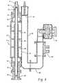
- Figure 1is a cross sectional view of a downstream plasma ashing apparatus
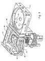
- Figure 2shows a perspective view of a microwave enclosure for use in a plasma asher apparatus
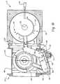
- Figure 3shows a cross sectional view which schematically shows a plasma generating component suitable for use with the downstream plasma ashing apparatus
- Figure 4shows perspective view of the plasma ashing apparatus
- Figure 5is a partial cutaway perspective view of a photoresist asher process chamber into which is installed a gas distribution system;
- Figure 6is a plan view of the gas distribution system in accordance with one embodiment
- Figure 7is a sectional view of the baffle plate assembly of Figure 6 , taken along lines 7-7;
- Figure 8is a plan view of the gas distribution system in accordance with another embodiment
- Figure 9is a perspective view of a loadlock chamber assembly and process chamber for a downstream plasma ashing apparatus.
- Figure 10is a top plan view of the loadlock chamber assembly and the process chamber of Figure 9 .
- Figure 1generally illustrates an axial flow downstream plasma apparatus 10 suitable for use in removing photoresist, sidewall deposits, and post etch residues from substrates including low k dielectric materials.
- the plasma apparatus 10generally comprises a gas delivery component 12, a plasma-generating component 14, a processing chamber 16, and an exhaust assembly component 18.
- the various components, in combination,provide unexpected improvements, for example, in processing substrates with oxygen free and nitrogen free plasmas, wherein the substrates include carbon containing low k dielectric materials.
- Downstream axial flow plasma apparatuses particularly suitable for modification in the present disclosureare plasma ashers, such as for example, those microwave plasma ashers available under the trade name Fusion ES and commercially available from Axcelis Technologies Corporation. Portions of the microwave plasma asher are described in U.S. Pat. Nos. 5,498,308 and 4,341,592 , and PCT International Application No. WO/97/37055 . As will be discussed below, the disclosure is not limited to any particular plasma asher in this or in the following embodiments. For instance, an inductively coupled plasma reactor can be used.
- Carbon containing low k dielectricsare hereinafter defined as those carbon containing insulating materials suitable for use in the manufacture of integrated circuits or the like having a dielectric constant less than about 3.5.
- the carbon-containing low k dielectric materialsmay include pendant groups that contain carbon or may be carbon based wherein the backbone of the dielectric material is primarily comprised of an interconnecting network of carbon.
- Carbon containing low k dielectricscan generally be categorized as one of two types: organic and doped oxides.
- organic low k dielectric materialsinclude polyimides, benzocyclobutene, parylenes, diamond-like carbon, poly(arylene ethers), cyclotenes, fluorocarbons and the like, such as those dielectrics commercially available under the trademarks SiLK, or BCB.
- doped oxide low k dielectric materialsinclude methyl silsesquioxane, hydrogen silsesquioxanes, nanoporous oxides, carbon doped silicon dioxides, and the like, such as, for example, those dielectrics commercially available under the trademarks CORAL, BLACK DIAMOND and AURORA. Both types of carbon containing low-k materials exist in dense and porous versions. Porous versions thereof are commercially known under trademarks such as LKD, ORION, BOSS, or porous SiLK. Other carbon containing low k dielectric materials will be apparent to one of ordinary skill in the art in view of this disclosure.
- hydrogen containing low k dielectricsare hereinafter-defined as those hydrogen containing insulating materials suitable for use in the manufacture of integrated circuits or the like having a dielectric constant less than about 3.5.
- Many of the carbon containing low k dielectrics described aboveinclude one or more hydrogen atoms attached to the carbon atoms within its chemical structure.
- suitable hydrogen containing low k dielectric materials in the present disclosureare not intended to be limited to carbon containing structures.
- the gas delivery component 12preferably comprises a gas purifier 20 in fluid communication with a gas source 22 (for generating the oxygen free and nitrogen free plasma) and a gas inlet 23 of the plasma-generating component 14.
- An additional gas source(not shown) may be in fluid communication with the gas inlet 23 for providing in situ cleaning capabilities.
- the purifier 20is adapted to reduce the level of impurities to less than about 20 parts per million (ppm), with impurity levels less than about 5 ppm more preferred, with impurity levels less than about 1 ppm more preferred, and with less than about 100 parts per billion (ppb) most preferred.
- Suitable purifiers achieving these impurity levelsinclude those based on a metal gettering technology such as those gas purifiers commercially available under the trade name MONO TORR ® high flow purifiers from SAES Pure Gas, Inc.
- the use of the gas purifier 20 in fluid communication with the gas source 22 employed for forming the plasmareduces the level of contaminants to amounts effective for robust processing of low k dielectric substrates, and in particular, carbon containing low k dielectrics.
- Suitable gases for generating the oxygen free and nitrogen free plasmainclude, but are not intended to be limited to, hydrogen, helium, argon, neon, other inert gases, hydrocarbons, and combinations comprising one or more of the foregoing gases.
- a helium gas source having a reported purity of 99.999%can be undesirable for plasma mediated processing of carbon based low k dielectrics.
- Impuritiessuch as H 2 O, O 2 , CO, CO 2 , and N 2 , can be at levels sufficient to cause erosion of the low k dielectric during further processing of the substrate and/or deleteriously cause an increase in the dielectric constant.
- the incoming gas for forming the plasmais purified to contain less than about 20 ppm of H 2 O, O 2 , CO, CO 2 , and N 2 .
- the purifier 20is preferably selected to be efficient and provide these preferred impurity levels at relatively high flow rates, e.g., flow rates of about 1000 to about 12,000 standard cubic centimeters per minute (sccm) or more can be expected for a 300 mm downstream plasma asher. 200mm systems require proportionately smaller flow rates.
- relatively high flow ratese.g., flow rates of about 1000 to about 12,000 standard cubic centimeters per minute (sccm) or more can be expected for a 300 mm downstream plasma asher. 200mm systems require proportionately smaller flow rates.
- FIGs 2 and 3illustrate an exemplary microwave plasma-generating component 14 with which the present disclosure may be practiced.
- Figure 4illustrates a perspective view of the plasma ashing apparatus 10 including the microwave plasma-generating component and a perspective view of the process chamber 16.
- the plasma-generating component 14has been simplified to illustrate only those components that are relevant to an understanding of the present disclosure. Those of ordinary skill in the art will recognize that other components may be required to produce an operational plasma ashing apparatus 10. However, because such components are well known in the art, and because they do not further aid in the understanding of the present disclosure, a discussion of such components is not provided.
- the microwave plasma-generating component 14includes a microwave enclosure 24.
- the microwave enclosure 24is a rectangular box that is partitioned into lengthwise sections 26, 28, and 30 having plasma tube 32 passing therethrough. Each partition has an opening through which the plasma tube passes.
- Each sectionis fed with microwave energy during operation. Thus, each section appears to be a relatively short cavity to the incoming microwave energy, promoting the formation of modes having azithumal and axial uniformity.
- Outer tube 34surrounds the plasma tube inside the cavity. The outer tube is slightly separated from the plasma tube and air, under positive pressure, is fed between the two tubes to provide effective cooling of the plasma tube.
- Tube 34is preferably made of sapphire. Other plasma tube materials such as quartz, alumina-coated quartz, or ceramics can be used.
- the microwave enclosure 24is dimensioned to support the rectangular TM 110 mode and the enclosure 24 may have a square cross section.
- the dimensions of the cross sectionsare such that the TM 110 mode is resonant.
- the length of each sectionis less than ⁇ g/ 2 where X g is the guide length within the cavity of the TE 101 mode.
- the openings in the partitions 26, 28, and 30 through which the concentric tubes are fedare made larger than the exterior dimension of the plasma tube.
- an iris plate 36which covers the open side of the microwave structure and is effective to feed microwave energy into adjacent sections.
- Plate 36is a flat metallic plate having irises 38, 40, 42, 44, through which the microwave energy is fed.
- Microwave traps 46 and 48are provided at the ends to prevent microwave transmission. Such traps may be of the type disclosed in U.S. Pat. No. 5,498,308 . Air seals/directional feeders 50 and 52 are provided for admitting cooling air and feeding it to the space between the concentric tubes. Air seals/directional feeder 54 are shown at the outlet end and a fourth such unit is present but is not seen.
- Magnetron 56provides microwave power that is fed through coupler 58 to a waveguide supplying TE 10 mode, having mutually perpendicular sections 60 and 62.
- the length of waveguide section 62is adjustable with moveable plunger 64.
- the bottom plate of waveguide section 62is iris plate 66, which couples microwave energy into partitioned microwave structure 24, through which the plasma tube 32 extends; thus plasma is excited in the gas mixture flowing through the plasma tube.
- end cap 70abuts microwave trap 48, and fitting 74 having a central orifice for admitting gas to the plasma tube extends into the end cap.
- the gas supply 22is regulated by an external flow box (not shown).
- the gas purifier 20is disposed in fluid communication with the gas supply 22 and the gas inlet 23 (see Figure 1 ).
- the plasma tube 32is supported at this end by "o" ring 72 in the end cap.
- the outer tube 34is supported at its ends by abutment against microwave traps 46 and 48.
- Spacer 76is present to provide the proper spacing in relation to the process chamber.
- the other end of the plasma tubeis located in end member 78, and has an opening 80 for emitting plasma/gas into the process chamber 16.
- the conduit forming the opening 80is fitted with a narrow aperture fitting to create a pressure differential between the plasma tube 32 and the processing chamber 16, wherein the pressure is greater in the plasma tube 32.
- the pressure within the plasma tube 32preferably ranges from about 1 torr to about atmospheric pressure.
- the pressure within the process chamber during operationranges from about 100 millitorr to about atmospheric pressure.
- the opening 80 of the plasma tube 32is in fluid communication with an interior region of the process chamber 16. Since the plasma is discharged from a relatively narrow orifice (compared to the dimensions of the substrate to be processed) into the interior of the process chamber, a gas distribution system 100 to promote uniform plasma exposure onto the substrate is disposed within the process chamber 16. The gas distribution system 100 is disposed intermediate to the substrate and opening 80 of the plasma tube 32.
- the gas distribution system 100comprises one or more baffle plates above the wafer to promote even distribution of the plasma to the substrate surface.
- the baffle platespreferably include multiply stacked baffle plates, wherein each plate contains one or more apertures.
- the baffle plate assemblyis adapted to provide more uniform reactivity of reactive species in the plasma.
- hydrogen radicalsfor example, within a plasma, decrease in ashing efficiency as the hydrogen radicals travel from the center most impingement point in the axial flow reactor to the outer edges of the baffle plate. While not wanting to be bound by theory, it is believed that the reduction in activity of hydrogen radicals as these species flow to the outer edges of the baffle plate may be from a combination of two effects.
- the photoresist ashing byproducts and spent gas from the central portions of the wafermust flow past the edge of the wafer in order to reach the exhaust conduit 170 of the process chamber 16. This results in significant dilution of the active hydrogen radicals nearer the edge of the wafer compared to the more central portions and additionally provides more opportunities for the radicals closer to the edge to deactivate by reacting with the photoresist ashing byproducts that have been removed from the more central locations.
- Figures 5-8illustrate suitable gas distribution systems for use in the apparatus 10.
- the gas distribution system 100is a dual baffle plate assembly.
- Figure 5shows the process chamber 16 into which is incorporated a first embodiment of the gas distribution system or baffle plate assembly 100.
- the asher process chamber 16 having the baffle plate assembly 100 installed thereinis suitable for use in a 300 millimeter (mm) wafer processing system.
- the gas distribution system 100could also be adapted for use with 200 mm wafers, as would be appreciated by one of ordinary skill in the art in view of this disclosure.
- the gas distribution system 100 described hereinis shown as being implemented within a downstream plasma asher apparatus, it may also be used in other semiconductor manufacturing equipment, such as residue removal, stripping, and isotropic etching equipment.
- the baffle plate assembly 100comprises an upper apertured baffle plate 102 and a relatively larger lower apertured baffle plate 104 positioned generally parallel to each other and separated from one another.
- the baffle plate assembly 100is attached to a lower portion 106 of the process chamber that includes a cavity 108 in which a wafer 110 to be processed is placed.
- the baffle plates 102 and 104in addition to being oriented parallel to each other, are also oriented parallel to the wafer 110 being processed.
- a seal 112is provided at the interface between the baffle plate assembly 100 and the upper portion 106 of the process chamber, and resides within groove 114 in the lower baffle plate 104 (see Figure 7 ). Wafers are introduced into and removed from the process chamber via a load lock mechanism (not shown) via entry/exit passageway 116.
- a heater mechanism(discussed below), located under the lower portion 106 of the process chamber, heats the underside of the wafer 110 to a desired temperature during processing.
- the process chamber 16is typically installed within the plasma ashing apparatus 10 intermediate to the heater assembly (below) and plasma-generating component 14 (above) at the locations of holes 118.
- energized plasmagas leaving the relatively narrow orifice of the plasma tube 32 (see Figure 3 ) encounters the baffle plate assembly 100.
- the energized plasma flowing from the plasma tube 32first encounters a central area of upper baffle plate 102 that is substantially free of apertures. This central apertureless area has the function of eliminating the high axial gas velocity exiting the plasma tube 32 and accelerating the gas/plasma species in a radial direction in order to achieve proper operation of the plenum formed between the lower baffle plate 104 and the lid of the chamber.
- the plasmais then distributed into the process chamber cavity 108 via apertures 120 in the upper baffle plate 102 and apertures 122 in the lower baffle plate 104.
- the lower baffle plate 104may be actively cooled with a cooling medium flowing through internal cooling passages 124 via inlets 126 and outlets 128.
- the walls 130 of the lower portion 106 of the process chambermay also be actively cooled with a cooling medium flowing through internal cooling passages 132 via inlet 134 and outlet 136.
- the lower baffle plate 104as shown more clearly in Figures 6 and 7 , comprises an outer flange 138 and a generally planar portion 140 that contains the apertures 122. Mounting holes (not shown) may be provided in the lower baffle plate 16 for mounting the upper baffle plate 14 thereto by means of standoffs 144.
- the distance between the upper and lower baffle platesin part determines the pattern of gas flow through the baffle plate assembly 100. For a 300 mm plasma asher, the distance between the upper and low baffle plates, 102, 104, respectively, is preferably about 0.25 inches to about 2 inches, with a distance of about 0.5 to about 1.5 inches more preferred.
- FIG 6is a plan view of the 300 mm baffle plate assembly shown in Figure 5
- Figure 7is a sectional view of this example of the baffle plate assembly 100.
- the baffle plate assembly 100is mounted to the upper portion 106 of the process chamber via mounting holes 146 in the lower baffle plate flange 138.
- Apertures 122are provided in the lower baffle plate.
- the surface area of apertured portion 122is sufficient to cover the wafer 110 residing therebelow (see Figure 5 ).
- the size of the apertures 122increases from a centerpoint of the lower baffle plate to an outer edge.
- the increasing size of the apertures 122improves plasma uniformity for oxygen free and nitrogen free plasmas such as for use with carbon containing and/or hydrogen containing low k dielectrics.
- Figure 8illustrates a plan view of the lower baffle plate 104 in accordance with the first embodiment.
- the lower baffle plateis preferably fabricated from quartz (SiO 2 ), sapphire coated quartz, sapphire, ceramic, or anodized aluminum
- the apertures 120 in the upper baffle plate 102are generally arranged in a radial or concentric multiply circular pattern.
- the upper baffle plate 102is comprised of sapphire-coated fused silica, quartz, sapphire, or a ceramic material.
- the apertures 120 in the upper baffle plate 102are preferably slightly larger than the largest apertures 122 in the lower baffle plate 104.
- Located at the center of the upper baffle plate 102is preferably an area free of apertures that may additionally comprise a sapphire, quartz or ceramic impingement plate 152.
- the center apertureless portion of upper baffle plate 102 with or without the impingement disk 152diverts energized gases emanating from the plasma tube 32 radially outward to the remaining apertured area of the upper baffle plate 102, so as to prevent the radially inward portion of the wafer 110 being processed from overheating, and thereby ashing at a proportionately higher rate than the rest of the wafer.
- the upper baffle plate 102can be configured to be apertureless, preferably for processing 200 mm wafers.
- Heating of the substrate 110is preferably accomplished by an array of tungsten halogen lamps 160 (see Figure 1 ) positioned below the wafer 110.
- a plate 156(the bottom wall of the process chamber as shown in Figure 5 ) transparent to visible and/or infrared radiation is disposed between the chamber 16 and the lamps 160.
- the substrateis heated from about 80° centrigrade (C) to about 350° C during ashing. More preferably, the substrate is stepwise heated by incrementally increasing the temperature. Heating has been found to increase the reaction rate of the plasma with the photoresist and/or post etch residues and consequently, increase throughput.
- the amount of heat applied to the substratewill depend on the thermal stability of the particular low k dielectric layer as well as the other layers and components already formed in the substrate. In a preferred embodiment, the amount of heat is applied non-uniformly to selected zones of the substrate to facilitate uniform reaction of the plasma with the photoresist.
- a controller(not shown) is in operative communication with the lamp array 160 for variously heating the substrate 110 to promote more uniform heating of the wafer during processing.
- An alternative method of heating the waferis to use a flat heated surface in contact or close proximity to heat the wafer, commonly referred to as a chuck.
- the substrate 110is preferably exposed to heat of sufficient intensity and duration to cause volatile contaminants to diffuse out of the low-k dielectric layer and volatize without causing degradation of any other components or layers in the substrate.
- the waferis heated from about 20°C to about 400°C, with about 100°C to about 300°C more preferred.
- the waferis heated from about 80°C to a maximum of about 180°C.
- the maximum temperatures for organic dielectricsare dependent on the intrinsic properties of the organic low k material used and can be determined by thermal analysis techniques known to those skilled in the art. The temperature may be step-wise increased during processing or remain static throughout the drying process.
- the process chamber 16includes an exhaust opening 158 centrally disposed in the bottom plate 156.
- the exhaust opening 158is coaxial with the plasma tube 32.
- the operating pressures within the process chamber 16are preferably about 100 millitorr to about 3 torr, with about 200 millitorr to about 2 torr more preferred, and with about 500 millitorr to about 1.5 torr even more preferred.
- the process chamber 16may further include additional features depending on the application.
- a quartz windowmay be installed and a UV light source may be placed in proximity to the wafer.
- a non-columnar light sourcemay have a wavelength similar to UV excimer lasers that have been shown to enhance photoresist removal in bulk strip applications and as such, could be used in parallel with microwave plasma generated reactive gases.
- pre- and post-photoresist strip exposure to the light sourcecould also provide residue removal and implanted resist removal advantages.
- Overhead RF sources, optical ports, gas analyzers, additional light sources, and the likecould also be used either independently, or in combination, with the process chamber 16 providing an extremely flexible process platform.
- the exhaust assembly component 18includes an exhaust conduit 170 in fluid communication with an interior region of the process chamber 16.
- An inlet 172 of the exhaust conduit 170is fluidly attached to opening 158 in the bottom plate 156 of the process chamber 16.
- the exhaust conduit 170preferably has a substantially straight shape from inlet 172 to outlet 174, thereby minimizing high impact areas (e.g., sharp bends and curves in the conduit) and the propensity for buildup of photoresist material and plasma ashing byproducts at sharp bends.
- the exhaust conduit 170is fabricated from quartz.
- a minimum diameter of the exhaust conduit 170is preferably at least about 2 inches for a 300 mm ashing apparatus (about a 1.5 inch diameter or greater is preferred for a 200 mm plasma ashing apparatus).
- the outlet 174 of the exhaust conduit 170is preferably connected to vacuum system 176.
- An afterburner assembly 178is in operative communication with the exhaust conduit 170.
- a gas inlet 180 and gas source 182are in fluid communication with the exhaust conduit 170 and are positioned upstream from the afterburner assembly 178.
- the afterburner assembly 178is employed to generate a plasma discharge within the exhaust conduit 170 so as to volatilize photoresist material and byproducts discharged from the process chamber 16.
- the gas source 180is preferably a non-halogen based oxidizing gas such as oxygen.
- the oxidizing gasis introduced to the afterburner assembly immediately above the RF coils and spacedly apart (i.e., downstream) from the exhaust opening 158 of the process chamber 16. Entry of oxygen into the process chamber 16 can deleteriously affect the low dielectric material in the manner previously described and the hardware and process are designed to circumvent this.
- the afterburner assembly 178generally comprises an RF coil 183 wrapped about an exterior of the exhaust conduit 170 to inductively excite a gas mixture flowing through the exhaust conduit 170.
- the oxidizing gasis preferably introduced at inlet 180 upstream from the afterburner assembly 178.
- the RF coilcan be replaced by a microwave source for generating plasma with similar results.
- a throttle valve 184, foreline valve (not shown), vacuum pump 176, and other vacuum processing linesare disposed downstream from the afterburner assembly 178.
- the RF coils 183are connected to a suitable RF generator or power supply 186.
- the power supply frequencymay vary, typically ranging from 400 KHz to the preferred value of 13.56 MHz at less than 1 kilowatt, but may also be at higher frequencies and higher power. More preferably, an RF power of 300 watts (W) to 500 W is employed to inductively couple an oxygen species containing plasma in the exhaust conduit 170, which causes the organic matter contained therein to combust. As a result, deposition of photoresist material and plasma byproducts downstream from the process chamber is prevented and/or removed.
- the RF connectionsare typically made through an RF matchbox 188 and the coils 183 are energized at the beginning of the plasma ashing process.
- the oxygen containing (O 2 ) gas admixture passing through the coupled RF fieldproduces a plasma that effectively and efficiently combusts organic matter.
- the afterburner assembly 178is configured to simultaneously operate during plasma ashing processing of a substrate 110 in the process chamber 16.
- the exhaust conduit 170also includes an optical detection system 190.
- the optical detection system 190optically detects emission signals having particular wavelength ranges that correspond to the reactants and byproducts of the reaction between the plasma and the photoresist.
- the techniquerelies on detecting the change in the emission intensities of characteristic optical radiation from the reactants and by-products in the plasma.
- Excited atoms or moleculesemit light when electrons relax from a higher energy state to a lower energy state. Atoms and molecules of different chemical compounds emit a series of unique spectral lines. The emission intensity for each chemical compound within the plasma depends partly on the relative concentration of the chemical compound in the plasma.
- a typical optical emission spectroscopy apparatusoperates by measuring the emission intensities of the reactive species and the by-product of the reactive species and the photoresist For instance, the emission of light by the by-product decreases and finally stops when an endpoint is reached.
- the optical emission spectroscopy apparatussenses the declining emission intensity of the by-product to determine this endpoint.
- optical signals from the regions downstream from the discharge region of the afterburner assembly 178can be used to clearly indicate when the plasma is ignited. For example, an oxidizing agent such as oxygen is consumed when the plasma is ignited within the exhaust conduit 170 and combustion products are generated.
- the combustion productse.g., carbon monoxide, carbon dioxide, water and the like, are those typically encountered during plasma ashing of photoresist with oxygen containing plasmas. Since these species emit strong optical emission signals, an oxygen free and nitrogen free plasma process can be readily monitored for endpoint detection by analyzing the optical signals produced in the exhaust conduit plasma discharge region. Once the signal of the monitored species is undetectable, it can be presumed that endpoint has been reached. As previously discussed, the use of oxygen free and nitrogen free plasma processes are desired for removing photoresist masks and the like from substrates containing carbon containing and/or hydrogen containing low k dielectrics. Suitable oxygen free and nitrogen free plasma processes for use in the present disclosure are disclosed in US. Pat. No. 6,630,406 . The present process and apparatus provides a means for endpoint detection, which otherwise is generally difficult to directly detect in a process chamber in view of the optically non-emissive species generated during an oxygen free and nitrogen free plasma ashing process.
- the optical detection system 190is coupled to the exhaust conduit.
- Collection optics 192may be arranged outside the exhaust conduit 170 to collect the emission spectra thus passed. Since the exhaust conduit 170 is preferably fabricated from an optically transparent material such as quartz or sapphire, an optical port or window is not necessary. In the event that an optically non-transparent material is employed for the fabrication of the exhaust conduit, an optical port of quartz or sapphire may be formed in the exhaust conduit.
- a spectrometer or monochromator,(generally shown as 194 in Figure 1 ) is arranged to receive light from the collection optics 192. Optical emission spectroscopy and techniques are generally well known on the art.
- the optical emission spectroscopyis by a spectrometer, such as a CCD (charge couple device) based spectrometer or a PDA (photodiode array) based spectrometer, that time sequentially records a wavelength range and converts the emission spectra into analog signals for subsequent analysis.
- narrow band filterscan be used to permit evaluation of specific ranges of the wavelength of interest on a light detector such as a PMT (photomultiplier tube) or a photodiode.
- the spectrometertime sequentially converts light signals emitted during the ashing process at specific wavelengths into an electrical analog signal, which can then be analyzed using methods known to those skilled in the art to produce a desired output.
- the datais viewed in real time.
- the datais viewed in graphical form showing the time evolution of the light intensity emitted during plasma processing for the wavelength range of interest.
- a monochromatorcan be used to collect the data.
- the monochromatorcan be configured with a photomultiplier tube, a photodiode or the like to record the emission signal.
- An example of a monochromator suitable for use in the present disclosureis model no. EP200MMD commercially available by the Verity Corporation.
- An example of a scanning monochromator suitable for use in the present disclosureis model no. EP200SMD commercially available by the Verity Corporation.
- Examples of CCD based spectrometers suitable for use in the present disclosureare Model Nos. SD1024 commercially available by Verity Corporation, and series PC2000 CCD spectrometers commercially available from Ocean Optics.
- An example of a photodetector array suitable for use in the present disclosureis model no. SPM9001 commercially available from the Prema Company, Germany.
- Figures 9 and 10illustrate a loadlock chamber assembly 200 coupled to the process chamber 16.
- the loadlock chamber assembly 200 and the process chamber 16are interconnected, wherein a closable vacuum sealed opening 202 is disposed and configured for permitting the exchange of wafers between the process chamber and the loadlock chamber assembly 200.
- the opening 202as shown, is configured for permitting a single wafer to be passed therethrough.
- opening 202may be sized and configured to allow two wafers to simultaneously pass through, e.g., a processed wafer exiting the process chamber and an unprocessed wafer entering the process chamber.
- the loadlock chamber assembly 200generally includes a removable sub-chamber 204 and a chamber 206.
- the sub-chamber 204is removably attached to a wall of the chamber 206 and preferably contains a dual end effector wafer transport mechanism such as described in U.S. Pat. No. 6,663,333 .
- the dual end effector wafer transport mechanismrobotically transports wafers into and out of the chambers 206 and 16 through opening 202. Since the articulating arms are housed in a removable sub-chamber 204 affixed to the loadlock chamber 206, the setup and repair of the robotic arms is simplified.
- the dual end effector wafer transport mechanismincludes an upper link arm 208 and a lower link arm 210 that share a common pivot axis 212 about which the arms articulate.
- the distal end of the upper link arm 208is pivotably connected to an upper translating arm 214 including an upper end effector 216 for holding a wafer or a substrate 104 (see Figure 1 ).
- the arm 208includes an elongated housing having a removable two-piece cover 230 and 232.
- the distal end of the lower link arm 210is pivotably connected to a lower translating arm 218 including a lower end effector 220.
- the arm 212also includes an elongated housing having a removable two-piece cover 230 and 232.
- the use of dual end effectors 216 and 220permits the loadlock chamber 206 to simultaneously contain two wafers at a midway point in the wafer exchange operation with the process chamber 16, thereby allowing high throughput.
- a cold plate 222is mounted approximately in the center of the loadlock chamber 206, and may be manually adjusted in the x-y plane, if necessary.
- the process chamber 16includes two wafer support pins (wafer pins) 224 and 226 for supporting a wafer 194 during processing.
- a thermocouple 193provides additional support for the wafer and provides a means for measuring the temperature of the wafer.
- the loadlock chamberprovides a mechanism for cooling the substrate to below 100°C.
- the loadlock chamber as described abovedoes not require venting between wafers, which could potentially introduce contaminants to the substrate.
- oxygen and nitrogenare detrimental to low k dielectric materials. Eliminating or minimizing contact with these gases is important to maintain the beneficial properties of the low k dielectric material.
- the plasma apparatus described aboveis used with substrates, wherein the low k materials contain carbon and/or hydrogen within its structure such as doped oxides, porous materials and organic low k films.
- the carbon-containing low k dielectric materialsmay include pendant groups that contain carbon or may be carbon based wherein the backbone of the dielectric material is primarily comprised of an interconnecting network of carbon.
- the ashing processincludes generating reactive species from a plasma gas mixture and exposing a substrate to the reactive species.
- the particular components of the plasma gas mixtureare selected by their ability to form a gas and plasma under plasma forming conditions.
- the gas mixture selectedis free from components that generate reactive oxygen species and reactive nitrogen species under plasma forming conditions. More preferably, the gas mixture is free from oxygen-containing compounds and nitrogen-containing compounds.
- the gas mixturemay include a number of reactive gases that are hydrogen-bearing such as hydrogen and hydrocarbons.
- the gas mixturemay further comprise an inert gas such as argon, helium, neon and the like.
- the plasma generated from the gas mixtureprimarily reacts with carbon and other atoms in the photoresist, polymers, and residues to form compounds that are volatile under the temperature and pressure conditions of the substrate and/or rinse removable compounds.
- the processis optimized to preferably have a selectivity greater than 50:1.
- Hydrogen-bearing gases suitable for use in the processinclude those compounds that contain hydrogen.
- the hydrogen-bearing gasesinclude hydrocarbons, hydrogen gas or mixtures thereof.
- Preferred hydrogen-bearing gasesexist in a gaseous state under plasma forming conditions and release hydrogen to form reactive hydrogen such as atomic hydrogen species and other hydrogen radicals under plasma forming conditions.
- the hydrocarbonsare generally unsubstituted.
- Examples of hydrogen-bearing hydrocarbon gasesinclude methane, ethane and propane.
- Preferred hydrogen-bearing gasesare mixtures of a hydrogen-bearing gas and a noble gas.
- noble gases suitable for use in the processinclude a gas in Group VIII of the periodic table such as argon, neon, helium and the like.
- a forming gas compositionthat includes a hydrogen and nitrogen gas mixture
- the use of nitrogen gas in the processis expressly excluded. Consequently, since forming gas is hereinafter defined as a gas containing a mixture of hydrogen and nitrogen gases, the use of forming gas in the process is expressly excluded.
- Particularly preferable for use in the present inventionis a gas mixture that includes hydrogen and helium gases. Helium gas atoms are light and readily diffuse to the substrate, which results in excellent carrier characteristics for plasma generated reactive hydrogen species.
- the percentage of hydrogen gas in the gas mixturegenerally does not exceed about 5 percent by volume of the gas mixture. However, higher amounts of hydrogen are acceptable and sometimes preferred for increasing the photoresist removal rate and selectivity.
- the amount of hydrogen in the gas mixtureis from about 1 to about 99 percent of the total volume. More preferably, the amount of hydrogen in the gas mixture is from about 10 to about 30 percent of the total volume.
- the semiconductor wafer 110 with photoresist and/or post etch residues thereon(and a carbon containing low k dielectric material) is placed into the process chamber 16 on wafer support pins.
- the wafer 110is preferably heated by infrared lamps 160 to accelerate the reaction of the photoresist and/or post etch residues with the plasma.
- the pressure within the process chamber 16is then reduced. Preferably, the pressure is maintained between about 1 torr to about 5 torr.
- An excitable oxygen free and nitrogen free gas mixtureis fed into the purifier and then the plasma tube 32 of the plasma generating component 14 via a gas inlet 24.
- Each section 26, 28, 30 of the plasma generating component 14is fed with microwave energy to excite a plasma in the plasma tube 32, which plasma is comprised of electrically neutral and charged particles.
- the charged particlesare preferably selectively removed before the plasma enters the process chamber 16.
- the excited or energetic atoms of the gasare fed into the process chamber and distributed uniformly across the wafer to react with the photoresist and/or post etch residues, which causes removal of the photoresist material and also forms volatile byproducts.
- the photoresist material and volatile byproductsare continuously swept away from the wafer surface to the centrally located exhaust conduit 170.
- a non-halogen oxidizing gassuch as oxygen is fed into the exhaust conduit downstream from the process chamber 16. No oxygen enters the process chamber 16.
- the afterburner assembly 178is energized to form high-density plasma within the exhaust conduit 170.
- the CCD spectrometertime sequentially records an emission spectrum that includes emission signals corresponding with the photoresist material and volatile byproducts, if present.
- the wavelength range of the emission spectrum monitoredis determined by the type of CCD spectrometer used and the presence of any filters used to eliminate certain wavelength emissions from reaching the CCD spectrometer.
- the CCD spectrometer configurationsimultaneously records the background radiation and the radiation from the emitted species during the ashing process.
- the background radiationcan be subtracted from the radiation resulting from the reaction of the plasma with the photoresist and/or byproducts.
- the emission peakrecords a change in intensity values and the conditions set by the end-point algorithm are met, the removal of photoresist and/or residues is complete, a signal is then sent to a control unit and the plasma can be turned off. The vacuum is released and the processed wafers may be removed from the process chamber. An optional rinse is used to remove any remaining residue on the stripped wafer.
- blank uncoated wafersare first exposed in the process chamber 16 and a first emission signal at a desired wavelength is measured.
- the first emission signalrepresents the background radiation as discussed above.
- substrates having photoresist and/or residues thereonare exposed to plasma in the process chamber.
- a second emission signal emitted at the desired wavelengthis recorded in the exhaust conduit by the monochromator.
- the background radiation of the first emission signalis subtracted from the second emission signal.
- the ashing endpointhas been reached and a signal is then sent to a control unit in the plasma asher and the plasma is turned off.
- the vacuumis then released and the processed wafers are removed from the reaction chamber.
- An optional rinseis then used to remove any remaining residues on the stripped wafer.
- the emission signalsof about 283nm, about 309 nm, about 387nm, about 431 nm, about 434 nm, about 468 nm, about 472 nm, about 513nm, about 516 nm, about 656nm, about 777 nm, and about 841nm ( ⁇ about 5 to about 10 nm) are monitored in the exhaust conduit
- These emission signalsrepresent spectral peaks for photoresist materials and plasma byproducts formed by a mixture of photoresist components, oxygen free and nitrogen free upstream plasmas and downstream afterburner plasmas.
- an oxygen free and nitrogen free plasmacan be used to remove the photoresist material and post etch residues from substrates containing carbon based low k dielectrics whereas a second plasma, preferably oxidizing, is formed in the exhaust conduit 170 to determine ashing endpoint for the oxygen free and nitrogen free plasma.
- the materials for fabricating the various components 12, 14, 16, and 18include metals, ceramics, glasses, polymers, composite materials, and combinations comprising at least one of the foregoing materials.
- suitable metalsinclude anodized aluminum, and/or stainless steel.
- Suitable ceramic materialsinclude silicon carbide, or aluminum oxide.
- plasma uniformitywas examined using different dual baffle plate configurations in a Fusion ES3 downstream microwave plasma asher commercially available from the Axcelis Technologies Corporation.
- Multiple 300 mm silicon waferswere coated with 0.75 microns of AZ1505 photoresist under identical conditions and exposed to a 4% hydrogen in helium plasma at 1.1 torr at the temperature indicated in Table 1.
- AZ1505 photoresistis commercially available by the Hoechst Corporation.
- the upper baffle plateswere identical for each configuration.
- a control lower baffle plateconsisting of 420 apertures evenly spaced across a 13" circular area was employed. Each aperture was 0.113 inches in diameter. Plasma uniformity for the control was compared to two different configurations in accordance with the teachings of the present disclosure.
- Configuration 1consisted of 570 apertures evenly spaced across a 15-inch circular area. Apertures within a 5-inch radius from the center were 0.113 inches in diameter. Those apertures outside the 5-inch radius had a 0.141-inch diameter.
- Configuration 2consisted of 420 apertures with increasing density from the centerpoint to the outer edge. The apertures had a diameter of 0.113 inches. In all cases, the distance between the upper and lower baffle plates was 0.5 inches and the distance between the substrate to the lower baffle plate was 0.5 inches. The time of exposure to the plasma was selected in order to remove approximately one half of the photoresist thickness.
- Non-uniformitywas measured by determining thickness removed at 49 points across the substrate using conventional techniques and then dividing the standard deviation for the 49 points by the average value and expressing the result as a percentage. Results are shown in Table 1. Table 1. Baffle Plate Assembly Processing Temperature (°C) Non-uniformity (%) Control 270 14.95 Configuration 1 270 8.18 Configuration 2 270 10.83 Control 330 9.61 Configuration 1 330 3.43 Configuration 2 330 7.38 The results show significant improvements in plasma ash uniformity by increasing density of the apertures and even more so by increasing the size of the apertures from the centerpoint of the lower baffle plate to the outer edge.
Landscapes
- Physics & Mathematics (AREA)
- Engineering & Computer Science (AREA)
- Plasma & Fusion (AREA)
- Chemical & Material Sciences (AREA)
- Analytical Chemistry (AREA)
- Drying Of Semiconductors (AREA)
Description
- The present disclosure relates to semiconductor apparatuses and processes, and more particularly, to plasma mediated processes and plasma apparatuses suitable for ashing organic material from a substrate including a low k dielectric material.
- Recently, much attention has been focused on developing low k dielectric thin films for use in the next generation of microelectronics. As integrated devices become smaller, the RC-delay time of signal propagation along interconnects becomes one of the dominant factors limiting overall chip speed. With the advent of copper technology, R has been pushed to its practical lowest limit so attention must be focused on reducing C. One way of accomplishing this task is to reduce the average dielectric constant (k) of the thin insulating films surrounding interconnects. The dielectric constant (k) of traditional silicon dioxide insulative materials is about 3.9. Lowering the dielectric constant (k) below 3.9 will provide a reduced capacitance and improve overall chip speed.
- Low k dielectric materials used in advanced integrated circuits typically comprise organic polymers or oxides and have dielectric constants less than about 3.5. The low k dielectric materials can be spun onto the substrate as a solution or deposited by a chemical vapor deposition process. Important low k film properties include thickness and uniformity, dielectric constant, refractive index, adhesion, chemical resistance, thermal stability, pore size and distribution, coefficient of thermal expansion, glass transition temperature, film stress, and copper diffusion coefficient.
- In fabricating integrated circuits on wafers, the wafers are generally subjected to many process steps before finished integrated circuits can be produced. Low k dielectric materials, especially carbon containing low k dielectric materials, can be sensitive to some of these process steps. For example, plasma used during an "ashing" step can strip both photoresist materials as well as remove a portion of the low-k dielectric film. Ashing generally refers to a plasma mediated stripping process by which residual photoresist and post etch residues are stripped or removed from a substrate upon exposure to the plasma. The ashing process generally occurs after an etching or implant process has been performed in which a photoresist material is used as a mask for etching a pattern into the underlying substrate or for selectively implanting ions into the exposed areas of the substrate. The remaining photoresist and any post etch or post implant residues on the wafer after the etch process or implant process is complete must be removed prior to further processing for numerous reasons generally known to those skilled in the art. The ashing step is typically followed by a wet chemical treatment to remove traces of the residue, which can cause further degradation of the low k dielectric, loss of material, and may also cause increase in the dielectric constant.
- It is important to note that ashing processes significantly differ from etching processes. Although both processes may be plasma mediated, an etching process is markedly different in that the plasma chemistry is chosen to permanently transfer an image into the substrate by removing portions of the substrate surface through openings in a photoresist mask. The plasma generally includes high-energy ion bombardment at low temperatures and low pressures (of the order of millitorr) to remove portions of the substrate. Moreover, the portions of the substrate exposed to the ions are generally removed at a rate equal to or greater than the removal rate of the photoresist mask. In contrast, ashing processes generally refer to selectively removing the photoresist mask and any polymers or residues formed during etching. The ashing plasma chemistry is much less aggressive than etching chemistries and is generally chosen to remove the photoresist mask layer at a rate much greater than the removal rate of the underlying substrate. Moreover, most ashing processes heat the substrate to temperatures greater than 200°C to increase the plasma reactivity, and are performed at relatively higher pressures (of the order of a torr). Thus, etching and ashing processes are directed to removal of significantly different materials and as such, require completely different plasma chemistries and processes. Successful ashing processes are not used to permanently transfer an image into the substrate. Rather, successful ashing processes are defined by the photoresist, polymer and residue removal rates without affecting or removing underlying layers, e.g., low k dielectric layers.
- Studies have suggested that a significant contribution to low k dielectric degradation during photoresist removal processes results from the use of oxygen and/or nitrogen and/or fluorine containing gas sources for generating ashing plasmas. Although gas mixtures containing one or more of these sources efficiently ash photoresist from the substrate, the use of these gas sources has proven detrimental to substrates containing low k dielectrics. For example, oxygen-containing plasmas are known to raise the dielectric constant of low k dielectric underlayers during plasma processing. The increases in dielectric constant affects, among others, interconnect capacitance, which directly impacts device performance. Moreover, the use of oxygen-containing plasmas is generally less preferred for advanced device fabrication employing copper metal layers since copper metal is readily oxidized. Occasionally, the damage caused by oxygen containing plasmas is not readily detected during metrology inspection of the substrate after plasma processing. However, the damage can be readily demonstrated and observed by a subsequent wet cleaning process, as may be typically employed after plasma ashing, wherein portions of the carbon and/or hydrogen-containing low k dielectric material are removed. The removed portions of the dielectric material are a source of variation in the critical dimension (CD) of the feature that is frequently unacceptable and impacts overall device yield. Moreover, even if a wet clean process is not included, the electrical and mechanical properties of the dielectric material may be changed by exposure to the oxygen-free plasmas thereby affecting operating performance. It is believed that carbon is depleted from the dielectric material during the oxygen containing plasma exposure.
- Ideally, the ashing plasma should not affect the underlying low k dielectric layers and preferentially removes only the photoresist material. The use of traditional dielectrics (higher k values) such as SiO2 provided high selectivity with these gas sources and was suitable for earlier device generation. However, in order to minimize damage to the low k dielectric, oxygen free and nitrogen free plasma processes have been developed. One such process includes generating plasma from a gas mixture comprising helium and hydrogen resulting in a different mechanism of removal. The oxygen free and nitrogen free plasma such as the plasma formed from helium and hydrogen is less aggressive and does not completely react with the photoresist in the traditional sense. Rather, it is believed that the plasma renders portions of the photoresist to be removable such as by sublimation. As a result of the mechanism of removal, while effective for removing photoresist material from the substrate, the plasma exposure tends to deposit large bodies of the sublimed or removed photoresist and byproducts within the processing chamber and in areas downstream from the plasma process chamber such as in the exhaust lines and any components therein. The buildup of ashing material can lead to short mean-time-between-clean (MTBC) and frequent rebuild/replacement of vacuum hardware resulting in loss of throughput and increased costs of ownership. Additionally, deposits of photoresist material within the process chamber that are located above the plane of the substrate can lead to particulate contamination on the substrate, thereby further affecting device yields.
- An additional problem with oxygen free and nitrogen free plasmas is the non-uniformity of the plasma exposure. Since these plasmas are less aggressive, non-uniformity is a significant issue. Some downstream plasma ashers have a narrow diameter orifice plasma tube in which the plasma is generated. The diameter of the substrate is generally much larger than the diameter of the plasma tube orifice. As such, baffle plates are typically positioned near the plasma tube outlet to deflect the plasma as it enters the process chamber such that the species in the plasma are uniformly dispersed across the substrate. However, it has been found that the less aggressive plasmas exhibit less ashing efficiency as reactive species are dispersed from the center point of the baffle plate to its outer edge resulting in hot spots, i.e., areas of non-uniformity. For example, it has been discovered that hydrogen radicals generated within a plasma decrease in ashing efficiency as the hydrogen radicals travel from the center most impingement point on the baffle plate in the axial flow reactor to the outer edges of the baffle plate. In chamber designs where the diameter of the wafer is comparable to that of the plasma tube, non-uniformity of radicals can be mitigated in other ways.
- Another problem with oxygen free and nitrogen free plasmas concerns endpoint detection. Traditional endpoint detection methods and apparatus are not suitable for use with these types of plasmas. For example, as in the case of plasma formed from a hydrogen and helium gas mixture, no optically excited species are emitted that are sufficient to generate a signal suitable for endpoint detection.
- Accordingly, there remains a need for improved processes and apparatuses for generating oxygen and nitrogen free plasmas for use with low k dielectrics.
EP 1,150,330 discloses a plasma processing system is provided, having processor chamber walls and/or a gas distribution or baffle plate equipped with integral cooling passages for reducing an operating temperature thereof during processing of a wafer by the system. Cooling medium inlets and outlets are connected to the cooling passages to permit circulation of a cooling medium through the cooling passages. Preferably, the chamber walls and the gas distribution or baffle plate are comprised of low-alloy anodized aluminum and the cooling passages are machined directly therein. The cooling medium may be either liquid (e.g., water) or gas (e.g., helium or nitrogen). The baffle plate comprises a generally planar, apertured, gas distribution central portion surrounded by a flange, into both of which the cooling passages may extend.; The cooling passages in the chamber walls and those in the gas distribution or baffle plate may be in communication with one another so as to permit them to share a single coolant circulating system. Alternatively, the cooling passages in the chamber walls and those in the gas distribution or baffle plate may not be in communication with one another, so as to provide independent circulating systems (gas or liquid) for each, thereby enabling independent temperature control and individual flow control thereof. In operation, the cooling medium in the chamber wall cooling passages is maintained approximately within the range of 15°C - 30°C, and the cooling medium in the gas distribution or baffle plate cooling passages is maintained approximately within the range of 15°C - 80°C.; Periodically, the lower baffle plate may alternatively be operated at up to 250°C to remove process residues from the surface of the plate that may otherwise condense and remain on the surface at lower operating temperatures (e.g., 15°C - 80°C).- According to the present invention there is provided an axial flow downstream plasma treatment device for treating a substrate, comprising, in combination: a gas source wherein the gas source is substantially free from nitrogen and oxygen; a plasma generating component in fluid communication with the gas source, the plasma generating component comprising a plasma tube and a plasma generator coupled to the plasma tube for generating a plasma within the plasma tube from the gas source; a gas purifier intermediate to the gas source and the plasma generator; a process chamber in fluid communication with the plasma tube comprising a baffle plate assembly at about an inlet of the process chamber, wherein the baffle plate assembly comprises a generally planar upper baffle plate fixedly positioned above a generally planar lower baffle plate, the lower baffle plate comprising a plurality of apertures disposed about a central axis, wherein the plurality of apertures increase in density from the central axis to an outer edge of the lower baffle plate and wherein the baffle plate assembly is positioned generally parallel to the substrate; and an exhaust conduit centrally located in a bottom wall of the process chamber.
- In another embodiment, an axial flow downstream plasma treatment device for treating a substrate containing a carbon and/or hydrogen containing low k dielectric layer, the plasma treatment device comprising, in combination, a gas source comprising substantially nitrogen free and oxygen free gases; a gas purifier in fluid communication with the gas source adapted to reduce nitrogen containing species and oxygen containing species from the substantially nitrogen free and oxygen free gases; a plasma generating component in fluid communication with the gas purifier, the plasma generating component comprising a plasma tube and a plasma generator coupled to the plasma tube for generating a plasma within the plasma tube from the purified nitrogen free and oxygen free gases; a process chamber in fluid communication with the plasma tube comprising a baffle plate assembly at an inlet of the process chamber; an exhaust conduit centrally located within the process chamber comprising a gas port in fluid communication with an oxidizing gas source; an afterburner assembly coupled to the exhaust conduit and adapted to generate a plasma, preferably oxidizing, in the exhaust conduit; and an optical detection system coupled to the exhaust conduit comprising collection optics focused within a plasma discharge region provided by the oxidizing plasma.
- In another embodiment, a process for uniformly distributing excited, species generated in an oxygen free and nitrogen free plasma onto a substrate, comprises introducing the excited species into a plasma processing chamber, wherein the plasma processing chamber comprises a baffle plate assembly for receiving the excited species, the baffle plate assembly comprising a generally planar upper baffle plate fixedly positioned above a generally planar lower baffle plate, the upper baffle plate being smaller than the lower baffle plate, the lower baffle plate comprising a plurality of apertures radially disposed about a central axis, wherein the plurality of apertures increase in density from the central axis to an outer edge of the lower baffle plate; and exposing the substrate to the excited species after flowing through baffle plate assembly.
- A plasma ashing process for removing photoresist material and post etch residues from a substrate containing a carbon and /or hydrogen containing low k dielectric layer comprises flowing a substantially oxygen free and nitrogen free gas into a gas purifier to form a purified gas with reduced levels of contaminants; forming a plasma from the purified gas; introducing the plasma into a process chamber, wherein the process chamber comprises a baffle plate assembly for receiving the plasma, the baffle plate assembly comprising a generally planar upper baffle plate fixedly positioned above a generally planar lower baffle plate, the upper baffle plate being smaller than the lower baffle plate, the lower baffle plate comprising a plurality of apertures radially disposed about a central axis, wherein the plurality of apertures increase in density on the central axis to an outer edge of the lower baffle plate; flowing the plasma through the baffle plate assembly and exposing the substrate to remove the photoresist material, post etch residues, and volatile byproducts from substrate; exhausting the removed photoresist material, post etch residues, and volatile byproducts into a centrally located exhaust conduit in the process chamber; selectively introducing an oxidizing gas into the exhaust conduit; forming a plasma from the oxidizing gas and the removed photoresist material , post etch residues, and volatile byproducts; optically monitoring an emission signal produced in the exhaust conduit plasma; and detecting an endpoint of the photoresist and post etch residues from an observed change in the emission signal.
- The above described and other features are exemplified by the following figures and detailed description.
- Referring to the exemplary drawings wherein like elements are numbered alike in the several Figures:
Figure 1 is a cross sectional view of a downstream plasma ashing apparatus; andFigure 2 shows a perspective view of a microwave enclosure for use in a plasma asher apparatus;Figure 3 shows a cross sectional view which schematically shows a plasma generating component suitable for use with the downstream plasma ashing apparatus;Figure 4 shows perspective view of the plasma ashing apparatus;Figure 5 is a partial cutaway perspective view of a photoresist asher process chamber into which is installed a gas distribution system;Figure 6 is a plan view of the gas distribution system in accordance with one embodiment;Figure 7 is a sectional view of the baffle plate assembly ofFigure 6 , taken along lines 7-7;Figure 8 is a plan view of the gas distribution system in accordance with another embodiment;Figure 9 is a perspective view of a loadlock chamber assembly and process chamber for a downstream plasma ashing apparatus; andFigure 10 is a top plan view of the loadlock chamber assembly and the process chamber ofFigure 9 .Figure 1 generally illustrates an axial flowdownstream plasma apparatus 10 suitable for use in removing photoresist, sidewall deposits, and post etch residues from substrates including low k dielectric materials. Theplasma apparatus 10 generally comprises agas delivery component 12, a plasma-generatingcomponent 14, aprocessing chamber 16, and anexhaust assembly component 18. The various components, in combination, provide unexpected improvements, for example, in processing substrates with oxygen free and nitrogen free plasmas, wherein the substrates include carbon containing low k dielectric materials.- Downstream axial flow plasma apparatuses particularly suitable for modification in the present disclosure are plasma ashers, such as for example, those microwave plasma ashers available under the trade name Fusion ES and commercially available from Axcelis Technologies Corporation. Portions of the microwave plasma asher are described in
U.S. Pat. Nos. 5,498,308 and4,341,592 , andPCT International Application No. WO/97/37055 - Carbon containing low k dielectrics are hereinafter defined as those carbon containing insulating materials suitable for use in the manufacture of integrated circuits or the like having a dielectric constant less than about 3.5. The carbon-containing low k dielectric materials may include pendant groups that contain carbon or may be carbon based wherein the backbone of the dielectric material is primarily comprised of an interconnecting network of carbon. Carbon containing low k dielectrics can generally be categorized as one of two types: organic and doped oxides. Examples of organic low k dielectric materials include polyimides, benzocyclobutene, parylenes, diamond-like carbon, poly(arylene ethers), cyclotenes, fluorocarbons and the like, such as those dielectrics commercially available under the trademarks SiLK, or BCB. Examples of doped oxide low k dielectric materials include methyl silsesquioxane, hydrogen silsesquioxanes, nanoporous oxides, carbon doped silicon dioxides, and the like, such as, for example, those dielectrics commercially available under the trademarks CORAL, BLACK DIAMOND and AURORA. Both types of carbon containing low-k materials exist in dense and porous versions. Porous versions thereof are commercially known under trademarks such as LKD, ORION, BOSS, or porous SiLK. Other carbon containing low k dielectric materials will be apparent to one of ordinary skill in the art in view of this disclosure.
- Likewise, hydrogen containing low k dielectrics are hereinafter-defined as those hydrogen containing insulating materials suitable for use in the manufacture of integrated circuits or the like having a dielectric constant less than about 3.5. Many of the carbon containing low k dielectrics described above include one or more hydrogen atoms attached to the carbon atoms within its chemical structure. However, suitable hydrogen containing low k dielectric materials in the present disclosure are not intended to be limited to carbon containing structures.
- As shown in
Figure 1 , thegas delivery component 12 preferably comprises agas purifier 20 in fluid communication with a gas source 22 (for generating the oxygen free and nitrogen free plasma) and agas inlet 23 of the plasma-generatingcomponent 14. An additional gas source (not shown) may be in fluid communication with thegas inlet 23 for providing in situ cleaning capabilities. In a preferred embodiment, thepurifier 20 is adapted to reduce the level of impurities to less than about 20 parts per million (ppm), with impurity levels less than about 5 ppm more preferred, with impurity levels less than about 1 ppm more preferred, and with less than about 100 parts per billion (ppb) most preferred. Suitable purifiers achieving these impurity levels include those based on a metal gettering technology such as those gas purifiers commercially available under the trade name MONO TORR® high flow purifiers from SAES Pure Gas, Inc. The use of thegas purifier 20 in fluid communication with thegas source 22 employed for forming the plasma reduces the level of contaminants to amounts effective for robust processing of low k dielectric substrates, and in particular, carbon containing low k dielectrics. Suitable gases for generating the oxygen free and nitrogen free plasma include, but are not intended to be limited to, hydrogen, helium, argon, neon, other inert gases, hydrocarbons, and combinations comprising one or more of the foregoing gases. For example, a helium gas source having a reported purity of 99.999% can be undesirable for plasma mediated processing of carbon based low k dielectrics. Impurities such as H2O, O2, CO, CO2, and N2, can be at levels sufficient to cause erosion of the low k dielectric during further processing of the substrate and/or deleteriously cause an increase in the dielectric constant. Preferably, the incoming gas for forming the plasma is purified to contain less than about 20 ppm of H2O, O2, CO, CO2, and N2. Thepurifier 20 is preferably selected to be efficient and provide these preferred impurity levels at relatively high flow rates, e.g., flow rates of about 1000 to about 12,000 standard cubic centimeters per minute (sccm) or more can be expected for a 300 mm downstream plasma asher. 200mm systems require proportionately smaller flow rates. Figures 2 and3 illustrate an exemplary microwave plasma-generatingcomponent 14 with which the present disclosure may be practiced.Figure 4 illustrates a perspective view of theplasma ashing apparatus 10 including the microwave plasma-generating component and a perspective view of theprocess chamber 16. It is to be understood that the plasma-generatingcomponent 14 has been simplified to illustrate only those components that are relevant to an understanding of the present disclosure. Those of ordinary skill in the art will recognize that other components may be required to produce an operationalplasma ashing apparatus 10. However, because such components are well known in the art, and because they do not further aid in the understanding of the present disclosure, a discussion of such components is not provided.- The microwave plasma-generating
component 14 includes amicrowave enclosure 24. Themicrowave enclosure 24 is a rectangular box that is partitioned intolengthwise sections plasma tube 32 passing therethrough. Each partition has an opening through which the plasma tube passes. Each section is fed with microwave energy during operation. Thus, each section appears to be a relatively short cavity to the incoming microwave energy, promoting the formation of modes having azithumal and axial uniformity.Outer tube 34 surrounds the plasma tube inside the cavity. The outer tube is slightly separated from the plasma tube and air, under positive pressure, is fed between the two tubes to provide effective cooling of the plasma tube.Tube 34 is preferably made of sapphire. Other plasma tube materials such as quartz, alumina-coated quartz, or ceramics can be used. Preferably, themicrowave enclosure 24 is dimensioned to support therectangular TM 110 mode and theenclosure 24 may have a square cross section. The dimensions of the cross sections are such that theTM 110 mode is resonant. The length of each section is less than λ g/ 2 where X g is the guide length within the cavity of the TE 101 mode. - The openings in the
partitions iris plate 36, which covers the open side of the microwave structure and is effective to feed microwave energy into adjacent sections.Plate 36 is a flat metallicplate having irises - Microwave traps 46 and 48 are provided at the ends to prevent microwave transmission. Such traps may be of the type disclosed in
U.S. Pat. No. 5,498,308 . Air seals/directional feeders directional feeder 54 are shown at the outlet end and a fourth such unit is present but is not seen. Magnetron 56 provides microwave power that is fed throughcoupler 58 to awaveguide supplying TE 10 mode, having mutuallyperpendicular sections waveguide section 62 is adjustable withmoveable plunger 64. The bottom plate ofwaveguide section 62 is iris plate 66, which couples microwave energy into partitionedmicrowave structure 24, through which theplasma tube 32 extends; thus plasma is excited in the gas mixture flowing through the plasma tube.- Referring again to
Figure 3 , it is seen thatend cap 70 abutsmicrowave trap 48, and fitting 74 having a central orifice for admitting gas to the plasma tube extends into the end cap. Thegas supply 22 is regulated by an external flow box (not shown). Thegas purifier 20 is disposed in fluid communication with thegas supply 22 and the gas inlet 23 (seeFigure 1 ). Theplasma tube 32 is supported at this end by "o"ring 72 in the end cap. Theouter tube 34 is supported at its ends by abutment against microwave traps 46 and 48.Spacer 76 is present to provide the proper spacing in relation to the process chamber. The other end of the plasma tube is located inend member 78, and has anopening 80 for emitting plasma/gas into theprocess chamber 16. Optionally, the conduit forming theopening 80 is fitted with a narrow aperture fitting to create a pressure differential between theplasma tube 32 and theprocessing chamber 16, wherein the pressure is greater in theplasma tube 32. During operation, the pressure within theplasma tube 32 preferably ranges from about 1 torr to about atmospheric pressure. In contrast, the pressure within the process chamber during operation ranges from about 100 millitorr to about atmospheric pressure. - The
opening 80 of theplasma tube 32 is in fluid communication with an interior region of theprocess chamber 16. Since the plasma is discharged from a relatively narrow orifice (compared to the dimensions of the substrate to be processed) into the interior of the process chamber, agas distribution system 100 to promote uniform plasma exposure onto the substrate is disposed within theprocess chamber 16. Thegas distribution system 100 is disposed intermediate to the substrate andopening 80 of theplasma tube 32. - In a preferred embodiment, the
gas distribution system 100 comprises one or more baffle plates above the wafer to promote even distribution of the plasma to the substrate surface. The baffle plates preferably include multiply stacked baffle plates, wherein each plate contains one or more apertures. In an especially preferred embodiment, the baffle plate assembly is adapted to provide more uniform reactivity of reactive species in the plasma. As discussed in the background section, it has been discovered that hydrogen radicals, for example, within a plasma, decrease in ashing efficiency as the hydrogen radicals travel from the center most impingement point in the axial flow reactor to the outer edges of the baffle plate. While not wanting to be bound by theory, it is believed that the reduction in activity of hydrogen radicals as these species flow to the outer edges of the baffle plate may be from a combination of two effects. First, in an axial flow reactor design such as the downstream plasma apparatus described herein, the photoresist ashing byproducts and spent gas from the central portions of the wafer must flow past the edge of the wafer in order to reach theexhaust conduit 170 of theprocess chamber 16. This results in significant dilution of the active hydrogen radicals nearer the edge of the wafer compared to the more central portions and additionally provides more opportunities for the radicals closer to the edge to deactivate by reacting with the photoresist ashing byproducts that have been removed from the more central locations. Second, because the distance to the edge is greater than the distance to the center it is more likely for the hydrogen radicals to deactivate from a process such as recombination to molecular hydrogen species. It has been discovered that better uniformity of ash rate can be achieved distally from the centerpoint of the baffle plate to the outer edges by increasing the aperture density of the baffle plate. For example, by increasing the aperture density from the centerpoint to the outer edges or by increasing the size of the apertures from the centerpoint of the baffle plate to the outer edges, or by including an apertureless centerpoint, or by a combination of one or more of the foregoing baffle plate configurations can increase reactivity and improve plasma uniformity at the substrate. Figures 5-8 illustrate suitable gas distribution systems for use in theapparatus 10. In a preferred embodiment, thegas distribution system 100 is a dual baffle plate assembly.Figure 5 shows theprocess chamber 16 into which is incorporated a first embodiment of the gas distribution system or baffleplate assembly 100. Theasher process chamber 16 having thebaffle plate assembly 100 installed therein is suitable for use in a 300 millimeter (mm) wafer processing system. Thegas distribution system 100 could also be adapted for use with 200 mm wafers, as would be appreciated by one of ordinary skill in the art in view of this disclosure. Moreover, although thegas distribution system 100 described herein is shown as being implemented within a downstream plasma asher apparatus, it may also be used in other semiconductor manufacturing equipment, such as residue removal, stripping, and isotropic etching equipment.- The
baffle plate assembly 100 comprises an upperapertured baffle plate 102 and a relatively larger lowerapertured baffle plate 104 positioned generally parallel to each other and separated from one another. Thebaffle plate assembly 100 is attached to alower portion 106 of the process chamber that includes acavity 108 in which awafer 110 to be processed is placed. Thebaffle plates wafer 110 being processed. - A
seal 112 is provided at the interface between thebaffle plate assembly 100 and theupper portion 106 of the process chamber, and resides withingroove 114 in the lower baffle plate 104 (seeFigure 7 ). Wafers are introduced into and removed from the process chamber via a load lock mechanism (not shown) via entry/exit passageway 116. A heater mechanism (discussed below), located under thelower portion 106 of the process chamber, heats the underside of thewafer 110 to a desired temperature during processing. - The
process chamber 16 is typically installed within theplasma ashing apparatus 10 intermediate to the heater assembly (below) and plasma-generating component 14 (above) at the locations ofholes 118. During operation, energized plasma (gas) leaving the relatively narrow orifice of the plasma tube 32 (seeFigure 3 ) encounters thebaffle plate assembly 100. In a preferred embodiment, the energized plasma flowing from theplasma tube 32 first encounters a central area ofupper baffle plate 102 that is substantially free of apertures. This central apertureless area has the function of eliminating the high axial gas velocity exiting theplasma tube 32 and accelerating the gas/plasma species in a radial direction in order to achieve proper operation of the plenum formed between thelower baffle plate 104 and the lid of the chamber. The plasma is then distributed into theprocess chamber cavity 108 viaapertures 120 in theupper baffle plate 102 andapertures 122 in thelower baffle plate 104. In one embodiment, thelower baffle plate 104 may be actively cooled with a cooling medium flowing throughinternal cooling passages 124 viainlets 126 andoutlets 128. Thewalls 130 of thelower portion 106 of the process chamber may also be actively cooled with a cooling medium flowing throughinternal cooling passages 132 viainlet 134 andoutlet 136. - The
lower baffle plate 104, as shown more clearly inFigures 6 and 7 , comprises anouter flange 138 and a generallyplanar portion 140 that contains theapertures 122. Mounting holes (not shown) may be provided in thelower baffle plate 16 for mounting theupper baffle plate 14 thereto by means of standoffs 144. The distance between the upper and lower baffle plates in part determines the pattern of gas flow through thebaffle plate assembly 100. For a 300 mm plasma asher, the distance between the upper and low baffle plates, 102, 104, respectively, is preferably about 0.25 inches to about 2 inches, with a distance of about 0.5 to about 1.5 inches more preferred. Figure 6 is a plan view of the 300 mm baffle plate assembly shown inFigure 5 , andFigure 7 is a sectional view of this example of thebaffle plate assembly 100. As shown in these Figures, thebaffle plate assembly 100 is mounted to theupper portion 106 of the process chamber via mountingholes 146 in the lowerbaffle plate flange 138.Apertures 122 are provided in the lower baffle plate. The surface area ofapertured portion 122 is sufficient to cover thewafer 110 residing therebelow (seeFigure 5 ). In this example, the size of theapertures 122 increases from a centerpoint of the lower baffle plate to an outer edge. The increasing size of theapertures 122 improves plasma uniformity for oxygen free and nitrogen free plasmas such as for use with carbon containing and/or hydrogen containing low k dielectrics.Figure 8 illustrates a plan view of thelower baffle plate 104 in accordance with the first embodiment. There, the density of theapertures 122 increases as one transitions from the center point of thelower baffle plate 104 to the outer edge, wherein the sizes of the apertures are the same. The lower baffle plate is preferably fabricated from quartz (SiO2), sapphire coated quartz, sapphire, ceramic, or anodized aluminum- The
apertures 120 in theupper baffle plate 102 are generally arranged in a radial or concentric multiply circular pattern. Theupper baffle plate 102 is comprised of sapphire-coated fused silica, quartz, sapphire, or a ceramic material. Theapertures 120 in theupper baffle plate 102 are preferably slightly larger than thelargest apertures 122 in thelower baffle plate 104. Located at the center of theupper baffle plate 102 is preferably an area free of apertures that may additionally comprise a sapphire, quartz orceramic impingement plate 152. The center apertureless portion ofupper baffle plate 102 with or without theimpingement disk 152 diverts energized gases emanating from theplasma tube 32 radially outward to the remaining apertured area of theupper baffle plate 102, so as to prevent the radially inward portion of thewafer 110 being processed from overheating, and thereby ashing at a proportionately higher rate than the rest of the wafer. In an alternative embodiment, theupper baffle plate 102 can be configured to be apertureless, preferably for processing 200 mm wafers. - Heating of the
substrate 110 is preferably accomplished by an array of tungsten halogen lamps 160 (seeFigure 1 ) positioned below thewafer 110. A plate 156 (the bottom wall of the process chamber as shown inFigure 5 ) transparent to visible and/or infrared radiation is disposed between thechamber 16 and thelamps 160. Preferably, the substrate is heated from about 80° centrigrade (C) to about 350° C during ashing. More preferably, the substrate is stepwise heated by incrementally increasing the temperature. Heating has been found to increase the reaction rate of the plasma with the photoresist and/or post etch residues and consequently, increase throughput. The amount of heat applied to the substrate will depend on the thermal stability of the particular low k dielectric layer as well as the other layers and components already formed in the substrate. In a preferred embodiment, the amount of heat is applied non-uniformly to selected zones of the substrate to facilitate uniform reaction of the plasma with the photoresist. In this embodiment, a controller (not shown) is in operative communication with thelamp array 160 for variously heating thesubstrate 110 to promote more uniform heating of the wafer during processing. An alternative method of heating the wafer is to use a flat heated surface in contact or close proximity to heat the wafer, commonly referred to as a chuck. - The
substrate 110 is preferably exposed to heat of sufficient intensity and duration to cause volatile contaminants to diffuse out of the low-k dielectric layer and volatize without causing degradation of any other components or layers in the substrate. Preferably, for porous or non-porous doped oxide carbon containing low k dielectric materials the wafer is heated from about 20°C to about 400°C, with about 100°C to about 300°C more preferred. Preferably, for organic low k materials the wafer is heated from about 80°C to a maximum of about 180°C. The maximum temperatures for organic dielectrics are dependent on the intrinsic properties of the organic low k material used and can be determined by thermal analysis techniques known to those skilled in the art. The temperature may be step-wise increased during processing or remain static throughout the drying process. - Additionally, the
process chamber 16 includes anexhaust opening 158 centrally disposed in thebottom plate 156. Preferably, theexhaust opening 158 is coaxial with theplasma tube 32. - The operating pressures within the
process chamber 16 are preferably about 100 millitorr to about 3 torr, with about 200 millitorr to about 2 torr more preferred, and with about 500 millitorr to about 1.5 torr even more preferred. Moreover, theprocess chamber 16 may further include additional features depending on the application. For example, a quartz window may be installed and a UV light source may be placed in proximity to the wafer. Such a non-columnar light source may have a wavelength similar to UV excimer lasers that have been shown to enhance photoresist removal in bulk strip applications and as such, could be used in parallel with microwave plasma generated reactive gases. Moreover, pre- and post-photoresist strip exposure to the light source could also provide residue removal and implanted resist removal advantages. Overhead RF sources, optical ports, gas analyzers, additional light sources, and the like could also be used either independently, or in combination, with theprocess chamber 16 providing an extremely flexible process platform. - Coupled to the
process chamber 16 is theexhaust assembly component 18. Theexhaust assembly component 18 includes anexhaust conduit 170 in fluid communication with an interior region of theprocess chamber 16. Aninlet 172 of theexhaust conduit 170 is fluidly attached to opening 158 in thebottom plate 156 of theprocess chamber 16. Theexhaust conduit 170 preferably has a substantially straight shape frominlet 172 tooutlet 174, thereby minimizing high impact areas (e.g., sharp bends and curves in the conduit) and the propensity for buildup of photoresist material and plasma ashing byproducts at sharp bends. In a preferred embodiment, theexhaust conduit 170 is fabricated from quartz. A minimum diameter of the exhaust conduit 170 (and opening 156) is preferably at least about 2 inches for a 300 mm ashing apparatus (about a 1.5 inch diameter or greater is preferred for a 200 mm plasma ashing apparatus). By centrally locating theexhaust conduit 170 within theprocess chamber 16, flow from the plasma tube to the exhaust assembly is simplified and provides greater plasma uniformity. - The
outlet 174 of theexhaust conduit 170 is preferably connected to vacuum system 176. Anafterburner assembly 178 is in operative communication with theexhaust conduit 170. Agas inlet 180 andgas source 182 are in fluid communication with theexhaust conduit 170 and are positioned upstream from theafterburner assembly 178. Theafterburner assembly 178 is employed to generate a plasma discharge within theexhaust conduit 170 so as to volatilize photoresist material and byproducts discharged from theprocess chamber 16. As will be described in greater detail below, thegas source 180 is preferably a non-halogen based oxidizing gas such as oxygen. It is preferred that the oxidizing gas is introduced to the afterburner assembly immediately above the RF coils and spacedly apart (i.e., downstream) from theexhaust opening 158 of theprocess chamber 16. Entry of oxygen into theprocess chamber 16 can deleteriously affect the low dielectric material in the manner previously described and the hardware and process are designed to circumvent this. - The
afterburner assembly 178 generally comprises anRF coil 183 wrapped about an exterior of theexhaust conduit 170 to inductively excite a gas mixture flowing through theexhaust conduit 170. The oxidizing gas is preferably introduced atinlet 180 upstream from theafterburner assembly 178. The RF coil can be replaced by a microwave source for generating plasma with similar results. Athrottle valve 184, foreline valve (not shown), vacuum pump 176, and other vacuum processing lines are disposed downstream from theafterburner assembly 178. - The RF coils 183 are connected to a suitable RF generator or
power supply 186. The power supply frequency may vary, typically ranging from 400 KHz to the preferred value of 13.56 MHz at less than 1 kilowatt, but may also be at higher frequencies and higher power. More preferably, an RF power of 300 watts (W) to 500 W is employed to inductively couple an oxygen species containing plasma in theexhaust conduit 170, which causes the organic matter contained therein to combust. As a result, deposition of photoresist material and plasma byproducts downstream from the process chamber is prevented and/or removed. - The RF connections are typically made through an
RF matchbox 188 and thecoils 183 are energized at the beginning of the plasma ashing process. The oxygen containing (O2) gas admixture passing through the coupled RF field produces a plasma that effectively and efficiently combusts organic matter. Preferably, theafterburner assembly 178 is configured to simultaneously operate during plasma ashing processing of asubstrate 110 in theprocess chamber 16. - Additionally, the
exhaust conduit 170 also includes anoptical detection system 190. Theoptical detection system 190 optically detects emission signals having particular wavelength ranges that correspond to the reactants and byproducts of the reaction between the plasma and the photoresist. The technique relies on detecting the change in the emission intensities of characteristic optical radiation from the reactants and by-products in the plasma. Excited atoms or molecules emit light when electrons relax from a higher energy state to a lower energy state. Atoms and molecules of different chemical compounds emit a series of unique spectral lines. The emission intensity for each chemical compound within the plasma depends partly on the relative concentration of the chemical compound in the plasma. A typical optical emission spectroscopy apparatus operates by measuring the emission intensities of the reactive species and the by-product of the reactive species and the photoresist For instance, the emission of light by the by-product decreases and finally stops when an endpoint is reached. The optical emission spectroscopy apparatus senses the declining emission intensity of the by-product to determine this endpoint. Advantageously, optical signals from the regions downstream from the discharge region of theafterburner assembly 178 can be used to clearly indicate when the plasma is ignited. For example, an oxidizing agent such as oxygen is consumed when the plasma is ignited within theexhaust conduit 170 and combustion products are generated. The combustion products, e.g., carbon monoxide, carbon dioxide, water and the like, are those typically encountered during plasma ashing of photoresist with oxygen containing plasmas. Since these species emit strong optical emission signals, an oxygen free and nitrogen free plasma process can be readily monitored for endpoint detection by analyzing the optical signals produced in the exhaust conduit plasma discharge region. Once the signal of the monitored species is undetectable, it can be presumed that endpoint has been reached. As previously discussed, the use of oxygen free and nitrogen free plasma processes are desired for removing photoresist masks and the like from substrates containing carbon containing and/or hydrogen containing low k dielectrics. Suitable oxygen free and nitrogen free plasma processes for use in the present disclosure are disclosed inUS. Pat. No. 6,630,406 . The present process and apparatus provides a means for endpoint detection, which otherwise is generally difficult to directly detect in a process chamber in view of the optically non-emissive species generated during an oxygen free and nitrogen free plasma ashing process. - The
optical detection system 190 is coupled to the exhaust conduit.Collection optics 192 may be arranged outside theexhaust conduit 170 to collect the emission spectra thus passed. Since theexhaust conduit 170 is preferably fabricated from an optically transparent material such as quartz or sapphire, an optical port or window is not necessary. In the event that an optically non-transparent material is employed for the fabrication of the exhaust conduit, an optical port of quartz or sapphire may be formed in the exhaust conduit. A spectrometer or monochromator, (generally shown as 194 inFigure 1 ) is arranged to receive light from thecollection optics 192. Optical emission spectroscopy and techniques are generally well known on the art. In one embodiment, the optical emission spectroscopy is by a spectrometer, such as a CCD (charge couple device) based spectrometer or a PDA (photodiode array) based spectrometer, that time sequentially records a wavelength range and converts the emission spectra into analog signals for subsequent analysis. Optionally, narrow band filters can be used to permit evaluation of specific ranges of the wavelength of interest on a light detector such as a PMT (photomultiplier tube) or a photodiode. The spectrometer time sequentially converts light signals emitted during the ashing process at specific wavelengths into an electrical analog signal, which can then be analyzed using methods known to those skilled in the art to produce a desired output. Preferably, the data is viewed in real time. Preferably, the data is viewed in graphical form showing the time evolution of the light intensity emitted during plasma processing for the wavelength range of interest. - Alternatively, other optical detectors can be used. For instance, as discussed above, a monochromator can be used to collect the data. As is known to those skilled in the art the monochromator can be configured with a photomultiplier tube, a photodiode or the like to record the emission signal.
- These optical emission spectroscopy devices and suitable configurations within a plasma reaction chamber will be apparent to those skilled in the art in view of this disclosure. An example of a monochromator suitable for use in the present disclosure is model no. EP200MMD commercially available by the Verity Corporation. An example of a scanning monochromator suitable for use in the present disclosure is model no. EP200SMD commercially available by the Verity Corporation. Examples of CCD based spectrometers suitable for use in the present disclosure are Model Nos. SD1024 commercially available by Verity Corporation, and series PC2000 CCD spectrometers commercially available from Ocean Optics. An example of a photodetector array suitable for use in the present disclosure is model no. SPM9001 commercially available from the Prema Company, Germany.
Figures 9 and10 illustrate aloadlock chamber assembly 200 coupled to theprocess chamber 16. Theloadlock chamber assembly 200 and theprocess chamber 16 are interconnected, wherein a closable vacuum sealedopening 202 is disposed and configured for permitting the exchange of wafers between the process chamber and theloadlock chamber assembly 200. Theopening 202, as shown, is configured for permitting a single wafer to be passed therethrough. Alternatively, opening 202 may be sized and configured to allow two wafers to simultaneously pass through, e.g., a processed wafer exiting the process chamber and an unprocessed wafer entering the process chamber. Theloadlock chamber assembly 200 generally includes aremovable sub-chamber 204 and achamber 206. The sub-chamber 204 is removably attached to a wall of thechamber 206 and preferably contains a dual end effector wafer transport mechanism such as described inU.S. Pat. No. 6,663,333 . The dual end effector wafer transport mechanism robotically transports wafers into and out of thechambers opening 202. Since the articulating arms are housed in aremovable sub-chamber 204 affixed to theloadlock chamber 206, the setup and repair of the robotic arms is simplified.- The dual end effector wafer transport mechanism includes an
upper link arm 208 and alower link arm 210 that share acommon pivot axis 212 about which the arms articulate. The distal end of theupper link arm 208 is pivotably connected to an upper translatingarm 214 including anupper end effector 216 for holding a wafer or a substrate 104 (seeFigure 1 ). Thearm 208 includes an elongated housing having a removable two-piece cover - Similarly constructed, the distal end of the
lower link arm 210 is pivotably connected to a lower translatingarm 218 including alower end effector 220. Thearm 212 also includes an elongated housing having a removable two-piece cover dual end effectors loadlock chamber 206 to simultaneously contain two wafers at a midway point in the wafer exchange operation with theprocess chamber 16, thereby allowing high throughput. Acold plate 222 is mounted approximately in the center of theloadlock chamber 206, and may be manually adjusted in the x-y plane, if necessary. Theprocess chamber 16 includes two wafer support pins (wafer pins) 224 and 226 for supporting awafer 194 during processing. A thermocouple 193 provides additional support for the wafer and provides a means for measuring the temperature of the wafer. - Advantageously, the loadlock chamber provides a mechanism for cooling the substrate to below 100°C. Moreover, the loadlock chamber as described above does not require venting between wafers, which could potentially introduce contaminants to the substrate. As previously discussed, oxygen and nitrogen are detrimental to low k dielectric materials. Eliminating or minimizing contact with these gases is important to maintain the beneficial properties of the low k dielectric material.
- Preferably, the plasma apparatus described above is used with substrates, wherein the low k materials contain carbon and/or hydrogen within its structure such as doped oxides, porous materials and organic low k films. The carbon-containing low k dielectric materials may include pendant groups that contain carbon or may be carbon based wherein the backbone of the dielectric material is primarily comprised of an interconnecting network of carbon. The process employing the nitrogen-free and oxygen-free plasma provides high ashing selectivity and overcomes the problems noted in the prior art that occur from ashing photoresist, polymers and residues from carbon and/or hydrogen based low k dielectric materials. Moreover, the process alleviates the subsequent metal filling problems caused by nitrogen in the ashing plasma.
- The ashing process includes generating reactive species from a plasma gas mixture and exposing a substrate to the reactive species. The particular components of the plasma gas mixture are selected by their ability to form a gas and plasma under plasma forming conditions. The gas mixture selected is free from components that generate reactive oxygen species and reactive nitrogen species under plasma forming conditions. More preferably, the gas mixture is free from oxygen-containing compounds and nitrogen-containing compounds. The gas mixture may include a number of reactive gases that are hydrogen-bearing such as hydrogen and hydrocarbons. The gas mixture may further comprise an inert gas such as argon, helium, neon and the like. The plasma generated from the gas mixture primarily reacts with carbon and other atoms in the photoresist, polymers, and residues to form compounds that are volatile under the temperature and pressure conditions of the substrate and/or rinse removable compounds. The process is optimized to preferably have a selectivity greater than 50:1.
- Hydrogen-bearing gases suitable for use in the process include those compounds that contain hydrogen. The hydrogen-bearing gases include hydrocarbons, hydrogen gas or mixtures thereof. Preferred hydrogen-bearing gases exist in a gaseous state under plasma forming conditions and release hydrogen to form reactive hydrogen such as atomic hydrogen species and other hydrogen radicals under plasma forming conditions. The hydrocarbons are generally unsubstituted. Examples of hydrogen-bearing hydrocarbon gases include methane, ethane and propane.
- Preferred hydrogen-bearing gases are mixtures of a hydrogen-bearing gas and a noble gas. Examples of noble gases suitable for use in the process include a gas in Group VIII of the periodic table such as argon, neon, helium and the like. Although prior art oxygen-free plasmas generally use a forming gas composition that includes a hydrogen and nitrogen gas mixture, the use of nitrogen gas in the process is expressly excluded. Consequently, since forming gas is hereinafter defined as a gas containing a mixture of hydrogen and nitrogen gases, the use of forming gas in the process is expressly excluded. Particularly preferable for use in the present invention is a gas mixture that includes hydrogen and helium gases. Helium gas atoms are light and readily diffuse to the substrate, which results in excellent carrier characteristics for plasma generated reactive hydrogen species.
- For safety reasons, the percentage of hydrogen gas in the gas mixture generally does not exceed about 5 percent by volume of the gas mixture. However, higher amounts of hydrogen are acceptable and sometimes preferred for increasing the photoresist removal rate and selectivity. Preferably, the amount of hydrogen in the gas mixture is from about 1 to about 99 percent of the total volume. More preferably, the amount of hydrogen in the gas mixture is from about 10 to about 30 percent of the total volume.
- In operation, the
semiconductor wafer 110 with photoresist and/or post etch residues thereon (and a carbon containing low k dielectric material) is placed into theprocess chamber 16 on wafer support pins. Thewafer 110 is preferably heated byinfrared lamps 160 to accelerate the reaction of the photoresist and/or post etch residues with the plasma. The pressure within theprocess chamber 16 is then reduced. Preferably, the pressure is maintained between about 1 torr to about 5 torr. An excitable oxygen free and nitrogen free gas mixture is fed into the purifier and then theplasma tube 32 of theplasma generating component 14 via agas inlet 24. Eachsection plasma generating component 14 is fed with microwave energy to excite a plasma in theplasma tube 32, which plasma is comprised of electrically neutral and charged particles. The charged particles are preferably selectively removed before the plasma enters theprocess chamber 16. The excited or energetic atoms of the gas are fed into the process chamber and distributed uniformly across the wafer to react with the photoresist and/or post etch residues, which causes removal of the photoresist material and also forms volatile byproducts. The photoresist material and volatile byproducts are continuously swept away from the wafer surface to the centrally locatedexhaust conduit 170. - Simultaneously with plasma ashing, a non-halogen oxidizing gas such as oxygen is fed into the exhaust conduit downstream from the
process chamber 16. No oxygen enters theprocess chamber 16. Theafterburner assembly 178 is energized to form high-density plasma within theexhaust conduit 170. For anexhaust conduit 170 configured with a CCD based spectrometer, the CCD spectrometer time sequentially records an emission spectrum that includes emission signals corresponding with the photoresist material and volatile byproducts, if present. The wavelength range of the emission spectrum monitored is determined by the type of CCD spectrometer used and the presence of any filters used to eliminate certain wavelength emissions from reaching the CCD spectrometer. The CCD spectrometer configuration simultaneously records the background radiation and the radiation from the emitted species during the ashing process. Using standard algorithms known to those skilled in the art, the background radiation can be subtracted from the radiation resulting from the reaction of the plasma with the photoresist and/or byproducts. Once the emission peak records a change in intensity values and the conditions set by the end-point algorithm are met, the removal of photoresist and/or residues is complete, a signal is then sent to a control unit and the plasma can be turned off. The vacuum is released and the processed wafers may be removed from the process chamber. An optional rinse is used to remove any remaining residue on the stripped wafer. - In a plasma asher with a monochromator, blank uncoated wafers are first exposed in the
process chamber 16 and a first emission signal at a desired wavelength is measured. The first emission signal represents the background radiation as discussed above. Next, substrates having photoresist and/or residues thereon (and containing a carbon based low k dielectric material) are exposed to plasma in the process chamber. A second emission signal emitted at the desired wavelength is recorded in the exhaust conduit by the monochromator. The background radiation of the first emission signal is subtracted from the second emission signal. When the second emission signal at the desired wavelength reaches a steady state and is about the same or below the first emission signal, the ashing endpoint has been reached and a signal is then sent to a control unit in the plasma asher and the plasma is turned off. The vacuum is then released and the processed wafers are removed from the reaction chamber. An optional rinse is then used to remove any remaining residues on the stripped wafer. - Other monochromators, spectrometers or like configurations and operations thereof for monitoring the plasma byproducts discharged from the process chamber will be apparent to those skilled in the art in view of this disclosure. Preferably, the emission signals of about 283nm, about 309 nm, about 387nm, about 431 nm, about 434 nm, about 468 nm, about 472 nm, about 513nm, about 516 nm, about 656nm, about 777 nm, and about 841nm (± about 5 to about 10 nm) are monitored in the exhaust conduit These emission signals represent spectral peaks for photoresist materials and plasma byproducts formed by a mixture of photoresist components, oxygen free and nitrogen free upstream plasmas and downstream afterburner plasmas. In this manner, an oxygen free and nitrogen free plasma can be used to remove the photoresist material and post etch residues from substrates containing carbon based low k dielectrics whereas a second plasma, preferably oxidizing, is formed in the
exhaust conduit 170 to determine ashing endpoint for the oxygen free and nitrogen free plasma. - Unless otherwise specified, the materials for fabricating the
various components - The following examples are presented for illustrative purposes only, and are not intended to limit the scope of the disclosure.
- In this example, plasma uniformity was examined using different dual baffle plate configurations in a Fusion ES3 downstream microwave plasma asher commercially available from the Axcelis Technologies Corporation. Multiple 300 mm silicon wafers were coated with 0.75 microns of AZ1505 photoresist under identical conditions and exposed to a 4% hydrogen in helium plasma at 1.1 torr at the temperature indicated in Table 1. AZ1505 photoresist is commercially available by the Hoechst Corporation. The upper baffle plates were identical for each configuration. A control lower baffle plate consisting of 420 apertures evenly spaced across a 13" circular area was employed. Each aperture was 0.113 inches in diameter. Plasma uniformity for the control was compared to two different configurations in accordance with the teachings of the present disclosure. Configuration 1 consisted of 570 apertures evenly spaced across a 15-inch circular area. Apertures within a 5-inch radius from the center were 0.113 inches in diameter. Those apertures outside the 5-inch radius had a 0.141-inch diameter. Configuration 2 consisted of 420 apertures with increasing density from the centerpoint to the outer edge. The apertures had a diameter of 0.113 inches. In all cases, the distance between the upper and lower baffle plates was 0.5 inches and the distance between the substrate to the lower baffle plate was 0.5 inches. The time of exposure to the plasma was selected in order to remove approximately one half of the photoresist thickness. Non-uniformity was measured by determining thickness removed at 49 points across the substrate using conventional techniques and then dividing the standard deviation for the 49 points by the average value and expressing the result as a percentage. Results are shown in Table 1.
Table 1. Baffle Plate Assembly Processing Temperature (°C) Non-uniformity (%) Control 270 14.95 Configuration 1 270 8.18 Configuration 2 270 10.83 Control 330 9.61 Configuration 1 330 3.43 Configuration 2 330 7.38 - While the disclosure has been described with reference to a preferred embodiment, it will be understood by those skilled in the art that various changes may be made and equivalents may be substituted for elements thereof without departing from the scope of the invention. In addition, many modifications may be made to adapt a particular situation or material to the teachings of the invention without departing from the essential scope thereof. Therefore, it is intended that the invention not be limited to the particular embodiment disclosed as the best mode contemplated for carrying out this invention, but that the invention will include all embodiments falling within the scope of the appended claims.
Claims (5)
- An axial flow downstream plasma treatment device (10) for treating a substrate, comprising, in combination:a gas source (22) providing a gas;a plasma generating component (14) in fluid communication with the gas source (22), the plasma generating component (14) comprising a plasma tube (32) and a plasma generator coupled to the plasma tube (32) for generating a plasma within the plasma tube (32) from said gas provided by the gas source (22);a process chamber (16) in fluid communication with the plasma tube (32) comprising a baffle plate assembly (100) at about an inlet of the process chamber (16), wherein the baffle plate assembly (100) comprises a generally planar upper baffle plate (102) fixedly positioned above a generally planar lower baffle plate (104), the lower baffle plate (104) comprising a plurality of apertures (122) disposed about a central axis and wherein the baffle plate assembly (100) is positioned generally parallel to the substrate; andan exhaust conduit (170) centrally located in a bottom wall of the process chamber (16);characterized in thatsaid gas provided by said gas source (22) is substantially free from nitrogen and oxygen;a gas purifier (20) is provided intermediate to the gas source (22) and the plasma generator (14); andthe plurality of apertures (122) in the lower baffle plate increase in density from the central axis to an outer edge of the lower baffle plate.
- The axial flow downstream plasma treatment device of Claim 1, further comprising an afterburner assembly (178) coupled to the exhaust conduit (170), wherein the exhaust conduit (170) comprises a gas port intermediate to the process chamber (16) and the afterburner assembly (170).
- The axial flow downstream plasma treatment device of Claim 2, wherein the afterburner assembly (178) comprises means for generating plasma in the exhaust conduit (170).
- The axial flow downstream plasma treatment device of Claim 2, wherein the afterburner assembly (170) comprises an RF coil (183) wrapped about an exterior of the exhaust conduit (170), a matchbox (188) in electrical communication with the RF coil (183), and a power supply in electrical communication with the matchbox (188).
- The axial flow downstream plasma treatment device of Claim 1, further comprising an optical detection system (190) coupled to the exhaust conduit (170).
Applications Claiming Priority (2)
| Application Number | Priority Date | Filing Date | Title |
|---|---|---|---|
| US10/249,962US8580076B2 (en) | 2003-05-22 | 2003-05-22 | Plasma apparatus, gas distribution assembly for a plasma apparatus and processes therewith |
| EP04752976AEP1625605B1 (en) | 2003-05-22 | 2004-05-21 | Downstream plasma treatment device |
Related Parent Applications (1)
| Application Number | Title | Priority Date | Filing Date |
|---|---|---|---|
| EP04752976.3Division | 2004-05-21 |
Publications (3)
| Publication Number | Publication Date |
|---|---|
| EP2278608A2 EP2278608A2 (en) | 2011-01-26 |
| EP2278608A3 EP2278608A3 (en) | 2011-02-23 |
| EP2278608B1true EP2278608B1 (en) | 2012-06-20 |
Family
ID=33449401
Family Applications (2)
| Application Number | Title | Priority Date | Filing Date |
|---|---|---|---|
| EP10182480AExpired - LifetimeEP2278608B1 (en) | 2003-05-22 | 2004-05-21 | Plasma apparatus, gas distribution assembly for a plasma apparatus and processes therewith |
| EP04752976AExpired - LifetimeEP1625605B1 (en) | 2003-05-22 | 2004-05-21 | Downstream plasma treatment device |
Family Applications After (1)
| Application Number | Title | Priority Date | Filing Date |
|---|---|---|---|
| EP04752976AExpired - LifetimeEP1625605B1 (en) | 2003-05-22 | 2004-05-21 | Downstream plasma treatment device |
Country Status (8)
| Country | Link |
|---|---|
| US (1) | US8580076B2 (en) |
| EP (2) | EP2278608B1 (en) |
| JP (1) | JP4780411B2 (en) |
| KR (1) | KR101127714B1 (en) |
| CN (1) | CN1795530B (en) |
| DE (1) | DE602004032225D1 (en) |
| TW (1) | TWI273655B (en) |
| WO (1) | WO2004107414A2 (en) |
Families Citing this family (157)
| Publication number | Priority date | Publication date | Assignee | Title |
|---|---|---|---|---|
| US6838114B2 (en) | 2002-05-24 | 2005-01-04 | Micron Technology, Inc. | Methods for controlling gas pulsing in processes for depositing materials onto micro-device workpieces |
| US6821347B2 (en) | 2002-07-08 | 2004-11-23 | Micron Technology, Inc. | Apparatus and method for depositing materials onto microelectronic workpieces |
| KR100426816B1 (en)* | 2002-07-31 | 2004-04-14 | 삼성전자주식회사 | Plasma processing equipment having improved vacuum pressure control apparatus |
| US6955725B2 (en) | 2002-08-15 | 2005-10-18 | Micron Technology, Inc. | Reactors with isolated gas connectors and methods for depositing materials onto micro-device workpieces |
| US6926775B2 (en) | 2003-02-11 | 2005-08-09 | Micron Technology, Inc. | Reactors with isolated gas connectors and methods for depositing materials onto micro-device workpieces |
| US7335396B2 (en) | 2003-04-24 | 2008-02-26 | Micron Technology, Inc. | Methods for controlling mass flow rates and pressures in passageways coupled to reaction chambers and systems for depositing material onto microfeature workpieces in reaction chambers |
| US20040235299A1 (en)* | 2003-05-22 | 2004-11-25 | Axcelis Technologies, Inc. | Plasma ashing apparatus and endpoint detection process |
| US8580076B2 (en)* | 2003-05-22 | 2013-11-12 | Lam Research Corporation | Plasma apparatus, gas distribution assembly for a plasma apparatus and processes therewith |
| US7344755B2 (en) | 2003-08-21 | 2008-03-18 | Micron Technology, Inc. | Methods and apparatus for processing microfeature workpieces; methods for conditioning ALD reaction chambers |
| US7235138B2 (en)* | 2003-08-21 | 2007-06-26 | Micron Technology, Inc. | Microfeature workpiece processing apparatus and methods for batch deposition of materials on microfeature workpieces |
| US7422635B2 (en) | 2003-08-28 | 2008-09-09 | Micron Technology, Inc. | Methods and apparatus for processing microfeature workpieces, e.g., for depositing materials on microfeature workpieces |
| US7056806B2 (en) | 2003-09-17 | 2006-06-06 | Micron Technology, Inc. | Microfeature workpiece processing apparatus and methods for controlling deposition of materials on microfeature workpieces |
| US7282239B2 (en) | 2003-09-18 | 2007-10-16 | Micron Technology, Inc. | Systems and methods for depositing material onto microfeature workpieces in reaction chambers |
| US7323231B2 (en) | 2003-10-09 | 2008-01-29 | Micron Technology, Inc. | Apparatus and methods for plasma vapor deposition processes |
| US7581511B2 (en) | 2003-10-10 | 2009-09-01 | Micron Technology, Inc. | Apparatus and methods for manufacturing microfeatures on workpieces using plasma vapor processes |
| US7799685B2 (en)* | 2003-10-13 | 2010-09-21 | Mattson Technology, Inc. | System and method for removal of photoresist in transistor fabrication for integrated circuit manufacturing |
| US7647886B2 (en)* | 2003-10-15 | 2010-01-19 | Micron Technology, Inc. | Systems for depositing material onto workpieces in reaction chambers and methods for removing byproducts from reaction chambers |
| US7258892B2 (en) | 2003-12-10 | 2007-08-21 | Micron Technology, Inc. | Methods and systems for controlling temperature during microfeature workpiece processing, e.g., CVD deposition |
| US7892357B2 (en)* | 2004-01-12 | 2011-02-22 | Axcelis Technologies, Inc. | Gas distribution plate assembly for plasma reactors |
| US7584942B2 (en) | 2004-03-31 | 2009-09-08 | Micron Technology, Inc. | Ampoules for producing a reaction gas and systems for depositing materials onto microfeature workpieces in reaction chambers |
| US8133554B2 (en) | 2004-05-06 | 2012-03-13 | Micron Technology, Inc. | Methods for depositing material onto microfeature workpieces in reaction chambers and systems for depositing materials onto microfeature workpieces |
| US7699932B2 (en) | 2004-06-02 | 2010-04-20 | Micron Technology, Inc. | Reactors, systems and methods for depositing thin films onto microfeature workpieces |
| US20050284573A1 (en)* | 2004-06-24 | 2005-12-29 | Egley Fred D | Bare aluminum baffles for resist stripping chambers |
| US20050284371A1 (en)* | 2004-06-29 | 2005-12-29 | Mcfadden Robert S | Deposition apparatus for providing uniform low-k dielectric |
| KR20060014495A (en)* | 2004-08-11 | 2006-02-16 | 주식회사 유진테크 | Shower head of chemical vapor deposition system |
| JP4633425B2 (en)* | 2004-09-17 | 2011-02-16 | 東京エレクトロン株式会社 | Plasma processing apparatus and plasma processing method |
| US20060228889A1 (en)* | 2005-03-31 | 2006-10-12 | Edelberg Erik A | Methods of removing resist from substrates in resist stripping chambers |
| JP2009518854A (en)* | 2005-12-07 | 2009-05-07 | アクセリス テクノロジーズ インコーポレーテッド | Medium pressure plasma system for surface layer removal without substrate loss |
| CN100376723C (en)* | 2005-12-08 | 2008-03-26 | 北京北方微电子基地设备工艺研究中心有限责任公司 | Shielding plate for enhancing flow field uniformity |
| US7381651B2 (en)* | 2006-03-22 | 2008-06-03 | Axcelis Technologies, Inc. | Processes for monitoring the levels of oxygen and/or nitrogen species in a substantially oxygen and nitrogen-free plasma ashing process |
| US7655571B2 (en) | 2006-10-26 | 2010-02-02 | Applied Materials, Inc. | Integrated method and apparatus for efficient removal of halogen residues from etched substrates |
| KR100796980B1 (en)* | 2007-01-17 | 2008-01-22 | 피에스케이 주식회사 | Substrate Processing Apparatus and Method |
| US8715455B2 (en)* | 2007-02-06 | 2014-05-06 | Tokyo Electron Limited | Multi-zone gas distribution system for a treatment system |
| JP4952375B2 (en) | 2007-05-23 | 2012-06-13 | 株式会社明電舎 | Resist removing method and apparatus |
| JP2009016453A (en)* | 2007-07-02 | 2009-01-22 | Tokyo Electron Ltd | Plasma processing device |
| WO2009020881A1 (en)* | 2007-08-07 | 2009-02-12 | Pivotal Systems Corporation | Method and apparatus for identifying the chemical composition of a gas |
| JP4160104B1 (en)* | 2007-08-16 | 2008-10-01 | 株式会社アルバック | Ashing equipment |
| US8673080B2 (en) | 2007-10-16 | 2014-03-18 | Novellus Systems, Inc. | Temperature controlled showerhead |
| CN101488446B (en) | 2008-01-14 | 2010-09-01 | 北京北方微电子基地设备工艺研究中心有限责任公司 | Plasma processing apparatus and gas dispensing apparatus thereof |
| WO2009107718A1 (en) | 2008-02-27 | 2009-09-03 | 東京エレクトロン株式会社 | Plasma etching apparatus and plasma etching method |
| US9997325B2 (en) | 2008-07-17 | 2018-06-12 | Verity Instruments, Inc. | Electron beam exciter for use in chemical analysis in processing systems |
| US9493875B2 (en)* | 2008-09-30 | 2016-11-15 | Eugene Technology Co., Ltd. | Shower head unit and chemical vapor deposition apparatus |
| US20100130017A1 (en)* | 2008-11-21 | 2010-05-27 | Axcelis Technologies, Inc. | Front end of line plasma mediated ashing processes and apparatus |
| CN102395704B (en)* | 2009-02-13 | 2014-02-19 | 盖利姆企业私人有限公司 | Plasma deposition |
| KR101110080B1 (en)* | 2009-07-08 | 2012-03-13 | 주식회사 유진테크 | Substrate treatment method for selectively inserting diffusion plate |
| US9111729B2 (en) | 2009-12-03 | 2015-08-18 | Lam Research Corporation | Small plasma chamber systems and methods |
| US20110136346A1 (en)* | 2009-12-04 | 2011-06-09 | Axcelis Technologies, Inc. | Substantially Non-Oxidizing Plasma Treatment Devices and Processes |
| US9190289B2 (en) | 2010-02-26 | 2015-11-17 | Lam Research Corporation | System, method and apparatus for plasma etch having independent control of ion generation and dissociation of process gas |
| US8562742B2 (en)* | 2010-04-30 | 2013-10-22 | Applied Materials, Inc. | Apparatus for radial delivery of gas to a chamber and methods of use thereof |
| GB2492849A (en)* | 2010-07-29 | 2013-01-16 | Gen Electric | A high pressure drop muffling system |
| US8307943B2 (en) | 2010-07-29 | 2012-11-13 | General Electric Company | High pressure drop muffling system |
| JP5698043B2 (en)* | 2010-08-04 | 2015-04-08 | 株式会社ニューフレアテクノロジー | Semiconductor manufacturing equipment |
| US8999104B2 (en) | 2010-08-06 | 2015-04-07 | Lam Research Corporation | Systems, methods and apparatus for separate plasma source control |
| US9155181B2 (en) | 2010-08-06 | 2015-10-06 | Lam Research Corporation | Distributed multi-zone plasma source systems, methods and apparatus |
| US9967965B2 (en) | 2010-08-06 | 2018-05-08 | Lam Research Corporation | Distributed, concentric multi-zone plasma source systems, methods and apparatus |
| US9449793B2 (en) | 2010-08-06 | 2016-09-20 | Lam Research Corporation | Systems, methods and apparatus for choked flow element extraction |
| KR101201697B1 (en)* | 2010-09-20 | 2012-11-15 | 에스엔유 프리시젼 주식회사 | Cold trap for adhering monomer and Apparatus for depositing monomer using the same |
| JP5697389B2 (en)* | 2010-09-27 | 2015-04-08 | 東京エレクトロン株式会社 | Electrode plate for plasma etching and plasma etching processing apparatus |
| JP5256328B2 (en)* | 2010-10-28 | 2013-08-07 | 株式会社日立国際電気 | Substrate processing apparatus and semiconductor device manufacturing method |
| JP6060242B2 (en)* | 2010-11-30 | 2017-01-11 | 株式会社日立国際電気 | Substrate processing apparatus, semiconductor device manufacturing method, and baffle structure |
| KR101937115B1 (en) | 2011-03-04 | 2019-01-09 | 노벨러스 시스템즈, 인코포레이티드 | Hybrid ceramic showerhead |
| US9129778B2 (en) | 2011-03-18 | 2015-09-08 | Lam Research Corporation | Fluid distribution members and/or assemblies |
| JP5851899B2 (en)* | 2011-03-25 | 2016-02-03 | 東京エレクトロン株式会社 | Plasma processing equipment |
| TWI563552B (en)* | 2011-04-28 | 2016-12-21 | Lam Res Corp | Substantially non-oxidizing plasma treatment devices and processes |
| US9245717B2 (en) | 2011-05-31 | 2016-01-26 | Lam Research Corporation | Gas distribution system for ceramic showerhead of plasma etch reactor |
| US8562785B2 (en)* | 2011-05-31 | 2013-10-22 | Lam Research Corporation | Gas distribution showerhead for inductively coupled plasma etch reactor |
| CN103031543B (en)* | 2011-09-30 | 2014-12-17 | 北京北方微电子基地设备工艺研究中心有限责任公司 | Top electrode and plasma processing equipment using top electrode |
| US9177762B2 (en) | 2011-11-16 | 2015-11-03 | Lam Research Corporation | System, method and apparatus of a wedge-shaped parallel plate plasma reactor for substrate processing |
| US10283325B2 (en) | 2012-10-10 | 2019-05-07 | Lam Research Corporation | Distributed multi-zone plasma source systems, methods and apparatus |
| US8430202B1 (en) | 2011-12-28 | 2013-04-30 | General Electric Company | Compact high-pressure exhaust muffling devices |
| US9057388B2 (en)* | 2012-03-21 | 2015-06-16 | International Business Machines Corporation | Vacuum trap |
| CN103367510A (en)* | 2012-03-30 | 2013-10-23 | 生阳新材料科技有限公司 | Cooling plate |
| US9399951B2 (en) | 2012-04-17 | 2016-07-26 | General Electric Company | Modular louver system |
| US8511096B1 (en) | 2012-04-17 | 2013-08-20 | General Electric Company | High bleed flow muffling system |
| US8550208B1 (en) | 2012-04-23 | 2013-10-08 | General Electric Company | High pressure muffling devices |
| US9132436B2 (en) | 2012-09-21 | 2015-09-15 | Applied Materials, Inc. | Chemical control features in wafer process equipment |
| US9064948B2 (en) | 2012-10-22 | 2015-06-23 | Globalfoundries Inc. | Methods of forming a semiconductor device with low-k spacers and the resulting device |
| US10256079B2 (en) | 2013-02-08 | 2019-04-09 | Applied Materials, Inc. | Semiconductor processing systems having multiple plasma configurations |
| US9362130B2 (en) | 2013-03-01 | 2016-06-07 | Applied Materials, Inc. | Enhanced etching processes using remote plasma sources |
| US20150118855A1 (en)* | 2013-10-30 | 2015-04-30 | Nisene Technology Group | Microwave induced plasma decapsulation |
| US9484190B2 (en)* | 2014-01-25 | 2016-11-01 | Yuri Glukhoy | Showerhead-cooler system of a semiconductor-processing chamber for semiconductor wafers of large area |
| US10741365B2 (en)* | 2014-05-05 | 2020-08-11 | Lam Research Corporation | Low volume showerhead with porous baffle |
| US9309598B2 (en) | 2014-05-28 | 2016-04-12 | Applied Materials, Inc. | Oxide and metal removal |
| US20160033070A1 (en)* | 2014-08-01 | 2016-02-04 | Applied Materials, Inc. | Recursive pumping member |
| US9966240B2 (en) | 2014-10-14 | 2018-05-08 | Applied Materials, Inc. | Systems and methods for internal surface conditioning assessment in plasma processing equipment |
| US9355922B2 (en) | 2014-10-14 | 2016-05-31 | Applied Materials, Inc. | Systems and methods for internal surface conditioning in plasma processing equipment |
| US11637002B2 (en) | 2014-11-26 | 2023-04-25 | Applied Materials, Inc. | Methods and systems to enhance process uniformity |
| US10573496B2 (en) | 2014-12-09 | 2020-02-25 | Applied Materials, Inc. | Direct outlet toroidal plasma source |
| US9728437B2 (en) | 2015-02-03 | 2017-08-08 | Applied Materials, Inc. | High temperature chuck for plasma processing systems |
| US20160225652A1 (en) | 2015-02-03 | 2016-08-04 | Applied Materials, Inc. | Low temperature chuck for plasma processing systems |
| US9666415B2 (en)* | 2015-02-11 | 2017-05-30 | Ford Global Technologies, Llc | Heated air plasma treatment |
| US10378107B2 (en)* | 2015-05-22 | 2019-08-13 | Lam Research Corporation | Low volume showerhead with faceplate holes for improved flow uniformity |
| US10023959B2 (en) | 2015-05-26 | 2018-07-17 | Lam Research Corporation | Anti-transient showerhead |
| US9691645B2 (en) | 2015-08-06 | 2017-06-27 | Applied Materials, Inc. | Bolted wafer chuck thermal management systems and methods for wafer processing systems |
| US9741593B2 (en) | 2015-08-06 | 2017-08-22 | Applied Materials, Inc. | Thermal management systems and methods for wafer processing systems |
| US9349605B1 (en) | 2015-08-07 | 2016-05-24 | Applied Materials, Inc. | Oxide etch selectivity systems and methods |
| US10504700B2 (en) | 2015-08-27 | 2019-12-10 | Applied Materials, Inc. | Plasma etching systems and methods with secondary plasma injection |
| KR102477302B1 (en)* | 2015-10-05 | 2022-12-13 | 주성엔지니어링(주) | Substrate treatment apparatus having exhaust gas cracker and exhaust gas treatment method of the same |
| CN108780736B (en)* | 2016-01-26 | 2023-05-02 | 周星工程股份有限公司 | Substrate processing apparatus |
| US10522371B2 (en)* | 2016-05-19 | 2019-12-31 | Applied Materials, Inc. | Systems and methods for improved semiconductor etching and component protection |
| US10504754B2 (en) | 2016-05-19 | 2019-12-10 | Applied Materials, Inc. | Systems and methods for improved semiconductor etching and component protection |
| US9865484B1 (en) | 2016-06-29 | 2018-01-09 | Applied Materials, Inc. | Selective etch using material modification and RF pulsing |
| US10629473B2 (en) | 2016-09-09 | 2020-04-21 | Applied Materials, Inc. | Footing removal for nitride spacer |
| US9934942B1 (en) | 2016-10-04 | 2018-04-03 | Applied Materials, Inc. | Chamber with flow-through source |
| US10546729B2 (en) | 2016-10-04 | 2020-01-28 | Applied Materials, Inc. | Dual-channel showerhead with improved profile |
| US10163696B2 (en) | 2016-11-11 | 2018-12-25 | Applied Materials, Inc. | Selective cobalt removal for bottom up gapfill |
| US10026621B2 (en) | 2016-11-14 | 2018-07-17 | Applied Materials, Inc. | SiN spacer profile patterning |
| US10435787B2 (en)* | 2016-11-14 | 2019-10-08 | Applied Materials, Inc. | Hydrogen partial pressure control in a vacuum process chamber |
| US10566206B2 (en) | 2016-12-27 | 2020-02-18 | Applied Materials, Inc. | Systems and methods for anisotropic material breakthrough |
| US10431429B2 (en) | 2017-02-03 | 2019-10-01 | Applied Materials, Inc. | Systems and methods for radial and azimuthal control of plasma uniformity |
| US10319739B2 (en) | 2017-02-08 | 2019-06-11 | Applied Materials, Inc. | Accommodating imperfectly aligned memory holes |
| US10943834B2 (en) | 2017-03-13 | 2021-03-09 | Applied Materials, Inc. | Replacement contact process |
| US11276590B2 (en) | 2017-05-17 | 2022-03-15 | Applied Materials, Inc. | Multi-zone semiconductor substrate supports |
| US11276559B2 (en) | 2017-05-17 | 2022-03-15 | Applied Materials, Inc. | Semiconductor processing chamber for multiple precursor flow |
| JP7176860B6 (en) | 2017-05-17 | 2022-12-16 | アプライド マテリアルズ インコーポレイテッド | Semiconductor processing chamber to improve precursor flow |
| US10497579B2 (en) | 2017-05-31 | 2019-12-03 | Applied Materials, Inc. | Water-free etching methods |
| US10920320B2 (en) | 2017-06-16 | 2021-02-16 | Applied Materials, Inc. | Plasma health determination in semiconductor substrate processing reactors |
| US10541246B2 (en) | 2017-06-26 | 2020-01-21 | Applied Materials, Inc. | 3D flash memory cells which discourage cross-cell electrical tunneling |
| US10727080B2 (en) | 2017-07-07 | 2020-07-28 | Applied Materials, Inc. | Tantalum-containing material removal |
| US10541184B2 (en) | 2017-07-11 | 2020-01-21 | Applied Materials, Inc. | Optical emission spectroscopic techniques for monitoring etching |
| US10043674B1 (en) | 2017-08-04 | 2018-08-07 | Applied Materials, Inc. | Germanium etching systems and methods |
| US10297458B2 (en) | 2017-08-07 | 2019-05-21 | Applied Materials, Inc. | Process window widening using coated parts in plasma etch processes |
| CN107460116A (en)* | 2017-08-31 | 2017-12-12 | 同济大学苏州研究院 | One kind is used for the preferable sperm swim-up device of sperm |
| US10903054B2 (en)* | 2017-12-19 | 2021-01-26 | Applied Materials, Inc. | Multi-zone gas distribution systems and methods |
| US11328909B2 (en) | 2017-12-22 | 2022-05-10 | Applied Materials, Inc. | Chamber conditioning and removal processes |
| US10854426B2 (en) | 2018-01-08 | 2020-12-01 | Applied Materials, Inc. | Metal recess for semiconductor structures |
| US10964512B2 (en) | 2018-02-15 | 2021-03-30 | Applied Materials, Inc. | Semiconductor processing chamber multistage mixing apparatus and methods |
| US10679870B2 (en) | 2018-02-15 | 2020-06-09 | Applied Materials, Inc. | Semiconductor processing chamber multistage mixing apparatus |
| TWI766433B (en) | 2018-02-28 | 2022-06-01 | 美商應用材料股份有限公司 | Systems and methods to form airgaps |
| US10593560B2 (en) | 2018-03-01 | 2020-03-17 | Applied Materials, Inc. | Magnetic induction plasma source for semiconductor processes and equipment |
| US10319600B1 (en) | 2018-03-12 | 2019-06-11 | Applied Materials, Inc. | Thermal silicon etch |
| US10497573B2 (en) | 2018-03-13 | 2019-12-03 | Applied Materials, Inc. | Selective atomic layer etching of semiconductor materials |
| US10573527B2 (en) | 2018-04-06 | 2020-02-25 | Applied Materials, Inc. | Gas-phase selective etching systems and methods |
| US10490406B2 (en) | 2018-04-10 | 2019-11-26 | Appled Materials, Inc. | Systems and methods for material breakthrough |
| US10699879B2 (en) | 2018-04-17 | 2020-06-30 | Applied Materials, Inc. | Two piece electrode assembly with gap for plasma control |
| US10886137B2 (en) | 2018-04-30 | 2021-01-05 | Applied Materials, Inc. | Selective nitride removal |
| US10755941B2 (en) | 2018-07-06 | 2020-08-25 | Applied Materials, Inc. | Self-limiting selective etching systems and methods |
| US10872778B2 (en) | 2018-07-06 | 2020-12-22 | Applied Materials, Inc. | Systems and methods utilizing solid-phase etchants |
| US10672642B2 (en) | 2018-07-24 | 2020-06-02 | Applied Materials, Inc. | Systems and methods for pedestal configuration |
| US11049755B2 (en) | 2018-09-14 | 2021-06-29 | Applied Materials, Inc. | Semiconductor substrate supports with embedded RF shield |
| US10892198B2 (en) | 2018-09-14 | 2021-01-12 | Applied Materials, Inc. | Systems and methods for improved performance in semiconductor processing |
| US11062887B2 (en) | 2018-09-17 | 2021-07-13 | Applied Materials, Inc. | High temperature RF heater pedestals |
| US11417534B2 (en) | 2018-09-21 | 2022-08-16 | Applied Materials, Inc. | Selective material removal |
| US11682560B2 (en) | 2018-10-11 | 2023-06-20 | Applied Materials, Inc. | Systems and methods for hafnium-containing film removal |
| US11121002B2 (en) | 2018-10-24 | 2021-09-14 | Applied Materials, Inc. | Systems and methods for etching metals and metal derivatives |
| CN208835019U (en)* | 2018-11-12 | 2019-05-07 | 江苏鲁汶仪器有限公司 | Reaction chamber inner lining |
| US11437242B2 (en) | 2018-11-27 | 2022-09-06 | Applied Materials, Inc. | Selective removal of silicon-containing materials |
| CN111321391A (en)* | 2018-12-13 | 2020-06-23 | 夏泰鑫半导体(青岛)有限公司 | Spray head for semiconductor manufacturing |
| US11721527B2 (en) | 2019-01-07 | 2023-08-08 | Applied Materials, Inc. | Processing chamber mixing systems |
| US10920319B2 (en) | 2019-01-11 | 2021-02-16 | Applied Materials, Inc. | Ceramic showerheads with conductive electrodes |
| AU2020250025A1 (en) | 2019-03-26 | 2021-10-28 | 6K Inc. | Segmented liner and methods of use within a microwave plasma apparatus |
| US11332827B2 (en)* | 2019-03-27 | 2022-05-17 | Applied Materials, Inc. | Gas distribution plate with high aspect ratio holes and a high hole density |
| CN119980191A (en) | 2019-08-28 | 2025-05-13 | 朗姆研究公司 | Metal Deposition |
| US11515147B2 (en) | 2019-12-09 | 2022-11-29 | Micron Technology, Inc. | Material deposition systems, and related methods |
| TWI783382B (en)* | 2020-03-18 | 2022-11-11 | 日商國際電氣股份有限公司 | Substrate processing apparatus, exhaust apparatus, and manufacturing method of semiconductor device |
| JP7493389B2 (en)* | 2020-06-10 | 2024-05-31 | 東京エレクトロン株式会社 | Film forming apparatus and film forming method |
| CN115666005B (en)* | 2022-12-15 | 2023-02-24 | 赛福仪器承德有限公司 | Plasma etching machine |
Citations (3)
| Publication number | Priority date | Publication date | Assignee | Title |
|---|---|---|---|---|
| US5510011A (en)* | 1992-11-09 | 1996-04-23 | Canon Kabushiki Kaisha | Method for forming a functional deposited film by bias sputtering process at a relatively low substrate temperature |
| EP1098189A2 (en)* | 1999-11-05 | 2001-05-09 | Axcelis Technologies, Inc. | Method for detecting an end point for an oxygen free plasma process |
| WO2003010799A2 (en)* | 2001-07-24 | 2003-02-06 | Axcelis Technologies, Inc. | Plasma ashing process |
Family Cites Families (87)
| Publication number | Priority date | Publication date | Assignee | Title |
|---|---|---|---|---|
| US32300A (en)* | 1861-05-14 | Denis lenain | ||
| US12624A (en)* | 1855-04-03 | Island | ||
| US3141739A (en)* | 1959-05-14 | 1964-07-21 | Nuclear Technical Services Cor | Gas purification |
| US4341592A (en) | 1975-08-04 | 1982-07-27 | Texas Instruments Incorporated | Method for removing photoresist layer from substrate by ozone treatment |
| DE3248670A1 (en)* | 1982-12-30 | 1984-07-05 | Hoechst Ag, 6230 Frankfurt | POLYESTER MULTILAYER FILM WITH THERMOPLASTIC PRESERVABLE INTERIOR |
| US4773355A (en)* | 1985-06-10 | 1988-09-27 | Massachusetts Institute Of Technology | Growth of epitaxial films by chemical vapor deposition |
| JPS62294180A (en) | 1986-06-13 | 1987-12-21 | Canon Inc | Deposited film forming device using plasma CVD method |
| US4792378A (en) | 1987-12-15 | 1988-12-20 | Texas Instruments Incorporated | Gas dispersion disk for use in plasma enhanced chemical vapor deposition reactor |
| JPH03147318A (en)* | 1989-11-01 | 1991-06-24 | Hitachi Ltd | Etching end point determination device |
| US5212116A (en)* | 1990-06-18 | 1993-05-18 | At&T Bell Laboratories | Method for forming planarized films by preferential etching of the center of a wafer |
| JPH04236425A (en)* | 1991-01-21 | 1992-08-25 | Toshiba Corp | Plasma processing equipment |
| US5356673A (en) | 1991-03-18 | 1994-10-18 | Jet Process Corporation | Evaporation system and method for gas jet deposition of thin film materials |
| JPH0631104A (en)* | 1992-07-21 | 1994-02-08 | Toshiba Corp | High-purity gas purification method |
| JP2922757B2 (en)* | 1993-09-10 | 1999-07-26 | フュージョン システムズ コーポレイション | Resist oxidation apparatus having catalytic reactor |
| US5498308A (en) | 1994-02-25 | 1996-03-12 | Fusion Systems Corp. | Plasma asher with microwave trap |
| JP2872637B2 (en) | 1995-07-10 | 1999-03-17 | アプライド マテリアルズ インコーポレイテッド | Microwave plasma based applicator |
| AU6595096A (en)* | 1995-07-21 | 1997-02-18 | Ultrapure Systems, Inc. | Single gas purifier vessel and heat exchanger |
| US6045618A (en) | 1995-09-25 | 2000-04-04 | Applied Materials, Inc. | Microwave apparatus for in-situ vacuum line cleaning for substrate processing equipment |
| US6193802B1 (en) | 1995-09-25 | 2001-02-27 | Applied Materials, Inc. | Parallel plate apparatus for in-situ vacuum line cleaning for substrate processing equipment |
| US6194628B1 (en) | 1995-09-25 | 2001-02-27 | Applied Materials, Inc. | Method and apparatus for cleaning a vacuum line in a CVD system |
| US5552017A (en)* | 1995-11-27 | 1996-09-03 | Taiwan Semiconductor Manufacturing Company | Method for improving the process uniformity in a reactor by asymmetrically adjusting the reactant gas flow |
| US5965034A (en)* | 1995-12-04 | 1999-10-12 | Mc Electronics Co., Ltd. | High frequency plasma process wherein the plasma is executed by an inductive structure in which the phase and anti-phase portion of the capacitive currents between the inductive structure and the plasma are balanced |
| US6471822B1 (en)* | 1996-01-24 | 2002-10-29 | Applied Materials, Inc. | Magnetically enhanced inductively coupled plasma reactor with magnetically confined plasma |
| US5741363A (en)* | 1996-03-22 | 1998-04-21 | Advanced Technology Materials, Inc. | Interiorly partitioned vapor injector for delivery of source reagent vapor mixtures for chemical vapor deposition |
| US5614026A (en)* | 1996-03-29 | 1997-03-25 | Lam Research Corporation | Showerhead for uniform distribution of process gas |
| US5961851A (en)* | 1996-04-02 | 1999-10-05 | Fusion Systems Corporation | Microwave plasma discharge device |
| US6159297A (en)* | 1996-04-25 | 2000-12-12 | Applied Materials, Inc. | Semiconductor process chamber and processing method |
| US5819434A (en)* | 1996-04-25 | 1998-10-13 | Applied Materials, Inc. | Etch enhancement using an improved gas distribution plate |
| US6090210A (en) | 1996-07-24 | 2000-07-18 | Applied Materials, Inc. | Multi-zone gas flow control in a process chamber |
| US5928426A (en) | 1996-08-08 | 1999-07-27 | Novellus Systems, Inc. | Method and apparatus for treating exhaust gases from CVD, PECVD or plasma etch reactors |
| KR19990071626A (en) | 1996-09-24 | 1999-09-27 | 매튜스 죤 씨. | Method and apparatus for removing residues from a substrate in a sapphire plasma asher |
| US5844195A (en)* | 1996-11-18 | 1998-12-01 | Applied Materials, Inc. | Remote plasma source |
| US5994678A (en)* | 1997-02-12 | 1999-11-30 | Applied Materials, Inc. | Apparatus for ceramic pedestal and metal shaft assembly |
| TW376547B (en)* | 1997-03-27 | 1999-12-11 | Matsushita Electric Industrial Co Ltd | Method and apparatus for plasma processing |
| US5968275A (en) | 1997-06-25 | 1999-10-19 | Lam Research Corporation | Methods and apparatus for passivating a substrate in a plasma reactor |
| US6106625A (en)* | 1997-12-02 | 2000-08-22 | Applied Materials, Inc. | Reactor useful for chemical vapor deposition of titanium nitride |
| US6057645A (en)* | 1997-12-31 | 2000-05-02 | Eaton Corporation | Plasma discharge device with dynamic tuning by a movable microwave trap |
| JP4147608B2 (en)* | 1998-03-06 | 2008-09-10 | 東京エレクトロン株式会社 | Heat treatment equipment |
| US6203657B1 (en)* | 1998-03-31 | 2001-03-20 | Lam Research Corporation | Inductively coupled plasma downstream strip module |
| US6190507B1 (en) | 1998-07-24 | 2001-02-20 | The United States Of America As Represented By The Department Of Energy | Method for generating a highly reactive plasma for exhaust gas aftertreatment and enhanced catalyst reactivity |
| US6190732B1 (en)* | 1998-09-03 | 2001-02-20 | Cvc Products, Inc. | Method and system for dispensing process gas for fabricating a device on a substrate |
| US5986747A (en)* | 1998-09-24 | 1999-11-16 | Applied Materials, Inc. | Apparatus and method for endpoint detection in non-ionizing gaseous reactor environments |
| US6368567B2 (en) | 1998-10-07 | 2002-04-09 | Applied Materials, Inc. | Point-of-use exhaust by-product reactor |
| US6366346B1 (en)* | 1998-11-19 | 2002-04-02 | Applied Materials, Inc. | Method and apparatus for optical detection of effluent composition |
| US6263830B1 (en)* | 1999-04-12 | 2001-07-24 | Matrix Integrated Systems, Inc. | Microwave choke for remote plasma generator |
| US6565661B1 (en)* | 1999-06-04 | 2003-05-20 | Simplus Systems Corporation | High flow conductance and high thermal conductance showerhead system and method |
| US6415736B1 (en) | 1999-06-30 | 2002-07-09 | Lam Research Corporation | Gas distribution apparatus for semiconductor processing |
| JP2001023955A (en)* | 1999-07-07 | 2001-01-26 | Mitsubishi Electric Corp | Plasma processing equipment |
| US6422002B1 (en) | 1999-07-23 | 2002-07-23 | The United States Of America As Represented By The United States Department Of Energy | Method for generating a highly reactive plasma for exhaust gas aftertreatment and enhanced catalyst reactivity |
| US6281135B1 (en) | 1999-08-05 | 2001-08-28 | Axcelis Technologies, Inc. | Oxygen free plasma stripping process |
| US6255222B1 (en) | 1999-08-24 | 2001-07-03 | Applied Materials, Inc. | Method for removing residue from substrate processing chamber exhaust line for silicon-oxygen-carbon deposition process |
| US6346489B1 (en)* | 1999-09-02 | 2002-02-12 | Applied Materials, Inc. | Precleaning process for metal plug that minimizes damage to low-κ dielectric |
| US20050022839A1 (en)* | 1999-10-20 | 2005-02-03 | Savas Stephen E. | Systems and methods for photoresist strip and residue treatment in integrated circuit manufacturing |
| US6259072B1 (en)* | 1999-11-09 | 2001-07-10 | Axcelis Technologies, Inc. | Zone controlled radiant heating system utilizing focused reflector |
| US6503330B1 (en)* | 1999-12-22 | 2003-01-07 | Genus, Inc. | Apparatus and method to achieve continuous interface and ultrathin film during atomic layer deposition |
| KR100767762B1 (en)* | 2000-01-18 | 2007-10-17 | 에이에스엠 저펜 가부시기가이샤 | A CVD semiconductor-processing device provided with a remote plasma source for self cleaning |
| US6783627B1 (en)* | 2000-01-20 | 2004-08-31 | Kokusai Semiconductor Equipment Corporation | Reactor with remote plasma system and method of processing a semiconductor substrate |
| US6367412B1 (en)* | 2000-02-17 | 2002-04-09 | Applied Materials, Inc. | Porous ceramic liner for a plasma source |
| US6444039B1 (en)* | 2000-03-07 | 2002-09-03 | Simplus Systems Corporation | Three-dimensional showerhead apparatus |
| US6391146B1 (en) | 2000-04-11 | 2002-05-21 | Applied Materials, Inc. | Erosion resistant gas energizer |
| WO2001072377A2 (en)* | 2000-03-24 | 2001-10-04 | Applied Materials, Inc. | Treatment of hazardous gases in effluent |
| US6592817B1 (en) | 2000-03-31 | 2003-07-15 | Applied Materials, Inc. | Monitoring an effluent from a chamber |
| EP1277233A2 (en)* | 2000-04-25 | 2003-01-22 | Tokyo Electron Corporation | Method of depositing metal film and metal deposition cluster tool including supercritical drying/cleaning module |
| US6537419B1 (en)* | 2000-04-26 | 2003-03-25 | David W. Kinnard | Gas distribution plate assembly for providing laminar gas flow across the surface of a substrate |
| US6635117B1 (en)* | 2000-04-26 | 2003-10-21 | Axcelis Technologies, Inc. | Actively-cooled distribution plate for reducing reactive gas temperature in a plasma processing system |
| US6444040B1 (en)* | 2000-05-05 | 2002-09-03 | Applied Materials Inc. | Gas distribution plate |
| US6633391B1 (en)* | 2000-11-07 | 2003-10-14 | Applied Materials, Inc | Monitoring of film characteristics during plasma-based semi-conductor processing using optical emission spectroscopy |
| US6538734B2 (en) | 2000-11-29 | 2003-03-25 | Lightwind Corporation | Method and device utilizing real-time gas sampling |
| JP2002184758A (en)* | 2000-12-13 | 2002-06-28 | Seiko Epson Corp | Dry etching equipment |
| JP2002273168A (en)* | 2001-03-15 | 2002-09-24 | Alpha Tekku:Kk | Device and method for removal of hazard |
| US6761796B2 (en)* | 2001-04-06 | 2004-07-13 | Axcelis Technologies, Inc. | Method and apparatus for micro-jet enabled, low-energy ion generation transport in plasma processing |
| US20020144706A1 (en) | 2001-04-10 | 2002-10-10 | Davis Matthew F. | Remote plasma cleaning of pumpstack components of a reactor chamber |
| US6630406B2 (en)* | 2001-05-14 | 2003-10-07 | Axcelis Technologies | Plasma ashing process |
| US6951823B2 (en)* | 2001-05-14 | 2005-10-04 | Axcelis Technologies, Inc. | Plasma ashing process |
| US6663333B2 (en)* | 2001-07-13 | 2003-12-16 | Axcelis Technologies, Inc. | Wafer transport apparatus |
| JP2003158080A (en) | 2001-11-22 | 2003-05-30 | Mitsubishi Electric Corp | Semiconductor manufacturing apparatus, deposit removing method in semiconductor manufacturing apparatus, and semiconductor device manufacturing method |
| US6849559B2 (en)* | 2002-04-16 | 2005-02-01 | Tokyo Electron Limited | Method for removing photoresist and etch residues |
| US7101260B2 (en)* | 2002-07-29 | 2006-09-05 | Nanoclean Technologies, Inc. | Methods for resist stripping and other processes for cleaning surfaces substantially free of contaminants |
| US7270713B2 (en)* | 2003-01-07 | 2007-09-18 | Applied Materials, Inc. | Tunable gas distribution plate assembly |
| US20040152296A1 (en)* | 2003-02-04 | 2004-08-05 | Texas Instruments Incorporated | Hexamethyldisilazane treatment of low-k dielectric films |
| US6838300B2 (en)* | 2003-02-04 | 2005-01-04 | Texas Instruments Incorporated | Chemical treatment of low-k dielectric films |
| US6942753B2 (en)* | 2003-04-16 | 2005-09-13 | Applied Materials, Inc. | Gas distribution plate assembly for large area plasma enhanced chemical vapor deposition |
| US7115534B2 (en)* | 2003-05-19 | 2006-10-03 | Applied Materials, Inc. | Dielectric materials to prevent photoresist poisoning |
| US8580076B2 (en)* | 2003-05-22 | 2013-11-12 | Lam Research Corporation | Plasma apparatus, gas distribution assembly for a plasma apparatus and processes therewith |
| US20040235299A1 (en)* | 2003-05-22 | 2004-11-25 | Axcelis Technologies, Inc. | Plasma ashing apparatus and endpoint detection process |
| US20050241767A1 (en)* | 2004-04-30 | 2005-11-03 | Ferris David S | Multi-piece baffle plate assembly for a plasma processing system |
| US20110136346A1 (en)* | 2009-12-04 | 2011-06-09 | Axcelis Technologies, Inc. | Substantially Non-Oxidizing Plasma Treatment Devices and Processes |
- 2003
- 2003-05-22USUS10/249,962patent/US8580076B2/enactiveActive
- 2004
- 2004-05-21KRKR1020057022172Apatent/KR101127714B1/ennot_activeExpired - Fee Related
- 2004-05-21CNCN2004800140618Apatent/CN1795530B/ennot_activeExpired - Fee Related
- 2004-05-21DEDE602004032225Tpatent/DE602004032225D1/ennot_activeExpired - Lifetime
- 2004-05-21JPJP2006533307Apatent/JP4780411B2/ennot_activeExpired - Fee Related
- 2004-05-21WOPCT/US2004/016076patent/WO2004107414A2/enactiveApplication Filing
- 2004-05-21EPEP10182480Apatent/EP2278608B1/ennot_activeExpired - Lifetime
- 2004-05-21TWTW093114399Apatent/TWI273655B/ennot_activeIP Right Cessation
- 2004-05-21EPEP04752976Apatent/EP1625605B1/ennot_activeExpired - Lifetime
Patent Citations (3)
| Publication number | Priority date | Publication date | Assignee | Title |
|---|---|---|---|---|
| US5510011A (en)* | 1992-11-09 | 1996-04-23 | Canon Kabushiki Kaisha | Method for forming a functional deposited film by bias sputtering process at a relatively low substrate temperature |
| EP1098189A2 (en)* | 1999-11-05 | 2001-05-09 | Axcelis Technologies, Inc. | Method for detecting an end point for an oxygen free plasma process |
| WO2003010799A2 (en)* | 2001-07-24 | 2003-02-06 | Axcelis Technologies, Inc. | Plasma ashing process |
Also Published As
| Publication number | Publication date |
|---|---|
| TWI273655B (en) | 2007-02-11 |
| CN1795530A (en) | 2006-06-28 |
| KR101127714B1 (en) | 2012-03-23 |
| CN1795530B (en) | 2010-12-01 |
| WO2004107414A2 (en) | 2004-12-09 |
| KR20060003121A (en) | 2006-01-09 |
| EP1625605A2 (en) | 2006-02-15 |
| DE602004032225D1 (en) | 2011-05-26 |
| WO2004107414A3 (en) | 2005-08-11 |
| JP2007501535A (en) | 2007-01-25 |
| EP2278608A2 (en) | 2011-01-26 |
| US20040238123A1 (en) | 2004-12-02 |
| EP1625605B1 (en) | 2011-04-13 |
| EP2278608A3 (en) | 2011-02-23 |
| US8580076B2 (en) | 2013-11-12 |
| JP4780411B2 (en) | 2011-09-28 |
| TW200509246A (en) | 2005-03-01 |
Similar Documents
| Publication | Publication Date | Title |
|---|---|---|
| EP2278608B1 (en) | Plasma apparatus, gas distribution assembly for a plasma apparatus and processes therewith | |
| US8268181B2 (en) | Plasma ashing apparatus and endpoint detection process | |
| US20130248113A1 (en) | Substantially non-oxidizing plasma treatment devices and processes | |
| EP1706889B1 (en) | Gas distribution plate assembly for plasma reactors | |
| US7449416B2 (en) | Apparatus and plasma ashing process for increasing photoresist removal rate | |
| EP1098189B1 (en) | Method for detecting an end point for an oxygen free plasma process | |
| KR100495783B1 (en) | Parallel plate apparatus for in-situ vacuum line cleaning for substrate processing equipment | |
| KR101392646B1 (en) | A gas mixture for removing photoresist and post etch residue from low-k dielectric material and method of use thereof | |
| KR101233059B1 (en) | Apparatus and process for treating dielectric materials | |
| WO2012148370A1 (en) | Substantially non-oxidizing plasma treatment devices and processes | |
| US20130160793A1 (en) | Plasma generating apparatus and process for simultaneous exposure of a workpiece to electromagnetic radiation and plasma |
Legal Events
| Date | Code | Title | Description |
|---|---|---|---|
| PUAI | Public reference made under article 153(3) epc to a published international application that has entered the european phase | Free format text:ORIGINAL CODE: 0009012 | |
| PUAL | Search report despatched | Free format text:ORIGINAL CODE: 0009013 | |
| AC | Divisional application: reference to earlier application | Ref document number:1625605 Country of ref document:EP Kind code of ref document:P | |
| AK | Designated contracting states | Kind code of ref document:A2 Designated state(s):DE FR GB IT | |
| AK | Designated contracting states | Kind code of ref document:A3 Designated state(s):DE FR GB IT | |
| RIN1 | Information on inventor provided before grant (corrected) | Inventor name:FERRIS, DAVID Inventor name:BUCKLEY, THOMAS Inventor name:WALDFRIED, CARLO Inventor name:SRIVASTAVA, ASEEM Inventor name:SAKTHIVEL, PALANIKUMARAN Inventor name:PINGREE, RICHARD JR. Inventor name:BECKNELL, ALAN | |
| 17P | Request for examination filed | Effective date:20110823 | |
| GRAP | Despatch of communication of intention to grant a patent | Free format text:ORIGINAL CODE: EPIDOSNIGR1 | |
| GRAS | Grant fee paid | Free format text:ORIGINAL CODE: EPIDOSNIGR3 | |
| GRAA | (expected) grant | Free format text:ORIGINAL CODE: 0009210 | |
| AC | Divisional application: reference to earlier application | Ref document number:1625605 Country of ref document:EP Kind code of ref document:P | |
| AK | Designated contracting states | Kind code of ref document:B1 Designated state(s):DE FR GB IT | |
| REG | Reference to a national code | Ref country code:GB Ref legal event code:FG4D | |
| REG | Reference to a national code | Ref country code:DE Ref legal event code:R096 Ref document number:602004038346 Country of ref document:DE Effective date:20120816 | |
| PG25 | Lapsed in a contracting state [announced via postgrant information from national office to epo] | Ref country code:IT Free format text:LAPSE BECAUSE OF FAILURE TO SUBMIT A TRANSLATION OF THE DESCRIPTION OR TO PAY THE FEE WITHIN THE PRESCRIBED TIME-LIMIT Effective date:20120620 | |
| PLBE | No opposition filed within time limit | Free format text:ORIGINAL CODE: 0009261 | |
| STAA | Information on the status of an ep patent application or granted ep patent | Free format text:STATUS: NO OPPOSITION FILED WITHIN TIME LIMIT | |
| 26N | No opposition filed | Effective date:20130321 | |
| REG | Reference to a national code | Ref country code:DE Ref legal event code:R097 Ref document number:602004038346 Country of ref document:DE Effective date:20130321 | |
| GBPC | Gb: european patent ceased through non-payment of renewal fee | Effective date:20130521 | |
| PG25 | Lapsed in a contracting state [announced via postgrant information from national office to epo] | Ref country code:DE Free format text:LAPSE BECAUSE OF NON-PAYMENT OF DUE FEES Effective date:20131203 | |
| REG | Reference to a national code | Ref country code:DE Ref legal event code:R119 Ref document number:602004038346 Country of ref document:DE Effective date:20131203 | |
| REG | Reference to a national code | Ref country code:FR Ref legal event code:ST Effective date:20140131 | |
| PG25 | Lapsed in a contracting state [announced via postgrant information from national office to epo] | Ref country code:GB Free format text:LAPSE BECAUSE OF NON-PAYMENT OF DUE FEES Effective date:20130521 | |
| PG25 | Lapsed in a contracting state [announced via postgrant information from national office to epo] | Ref country code:FR Free format text:LAPSE BECAUSE OF NON-PAYMENT OF DUE FEES Effective date:20130531 |